US20120126229A1 - Interconnection structures and methods for transfer-printed integrated circuit elements with improved interconnection alignment tolerance - Google Patents
Interconnection structures and methods for transfer-printed integrated circuit elements with improved interconnection alignment toleranceDownload PDFInfo
- Publication number
- US20120126229A1 US20120126229A1US13/302,497US201113302497AUS2012126229A1US 20120126229 A1US20120126229 A1US 20120126229A1US 201113302497 AUS201113302497 AUS 201113302497AUS 2012126229 A1US2012126229 A1US 2012126229A1
- Authority
- US
- United States
- Prior art keywords
- substrate
- integrated circuit
- chiplet
- layer
- circuit elements
- Prior art date
- Legal status (The legal status is an assumption and is not a legal conclusion. Google has not performed a legal analysis and makes no representation as to the accuracy of the status listed.)
- Granted
Links
- 238000000034methodMethods0.000titleclaimsabstractdescription89
- 239000000758substrateSubstances0.000claimsabstractdescription301
- 239000004020conductorSubstances0.000claimsabstractdescription110
- 238000004519manufacturing processMethods0.000claimsabstractdescription26
- 239000010410layerSubstances0.000claimsdescription269
- 239000011241protective layerSubstances0.000claimsdescription44
- 239000000463materialSubstances0.000claimsdescription36
- 238000005530etchingMethods0.000claimsdescription21
- 229910052751metalInorganic materials0.000claimsdescription21
- 239000002184metalSubstances0.000claimsdescription21
- VYPSYNLAJGMNEJ-UHFFFAOYSA-NSilicium dioxideChemical compoundO=[Si]=OVYPSYNLAJGMNEJ-UHFFFAOYSA-N0.000claimsdescription16
- 238000012360testing methodMethods0.000claimsdescription13
- 239000012790adhesive layerSubstances0.000claimsdescription9
- 229910021417amorphous siliconInorganic materials0.000claimsdescription9
- 238000000059patterningMethods0.000claimsdescription8
- 235000012239silicon dioxideNutrition0.000claimsdescription8
- 239000000377silicon dioxideSubstances0.000claimsdescription8
- 238000003825pressingMethods0.000claimsdescription4
- 238000007639printingMethods0.000claimsdescription4
- 230000001681protective effectEffects0.000claimsdescription3
- 230000008569processEffects0.000description38
- 239000004065semiconductorSubstances0.000description25
- 235000012431wafersNutrition0.000description20
- 238000012545processingMethods0.000description18
- 239000011347resinSubstances0.000description13
- 229920005989resinPolymers0.000description13
- 239000010409thin filmSubstances0.000description13
- 238000013461designMethods0.000description12
- 239000000853adhesiveSubstances0.000description7
- 230000001070adhesive effectEffects0.000description7
- 239000011521glassSubstances0.000description7
- KRHYYFGTRYWZRS-UHFFFAOYSA-NFluoraneChemical compoundFKRHYYFGTRYWZRS-UHFFFAOYSA-N0.000description6
- 230000015572biosynthetic processEffects0.000description6
- 238000004544sputter depositionMethods0.000description6
- 238000000576coating methodMethods0.000description5
- 239000000523sampleSubstances0.000description5
- 239000002356single layerSubstances0.000description5
- 239000011248coating agentSubstances0.000description4
- 150000004767nitridesChemical class0.000description4
- 229910052710siliconInorganic materials0.000description4
- 239000010703siliconSubstances0.000description4
- XUIMIQQOPSSXEZ-UHFFFAOYSA-NSiliconChemical compound[Si]XUIMIQQOPSSXEZ-UHFFFAOYSA-N0.000description3
- 229910052782aluminiumInorganic materials0.000description3
- XAGFODPZIPBFFR-UHFFFAOYSA-NaluminiumChemical compound[Al]XAGFODPZIPBFFR-UHFFFAOYSA-N0.000description3
- 238000013459approachMethods0.000description3
- 238000000151depositionMethods0.000description3
- 230000003287optical effectEffects0.000description3
- 238000002161passivationMethods0.000description3
- 229920000642polymerPolymers0.000description3
- 239000000126substanceSubstances0.000description3
- 238000012546transferMethods0.000description3
- 238000010023transfer printingMethods0.000description3
- 229910001218Gallium arsenideInorganic materials0.000description2
- 150000001875compoundsChemical class0.000description2
- 230000008021depositionEffects0.000description2
- 239000004205dimethyl polysiloxaneSubstances0.000description2
- 235000013870dimethyl polysiloxaneNutrition0.000description2
- 230000000873masking effectEffects0.000description2
- 150000002739metalsChemical class0.000description2
- 238000012986modificationMethods0.000description2
- 230000004048modificationEffects0.000description2
- CXQXSVUQTKDNFP-UHFFFAOYSA-NoctamethyltrisiloxaneChemical compoundC[Si](C)(C)O[Si](C)(C)O[Si](C)(C)CCXQXSVUQTKDNFP-UHFFFAOYSA-N0.000description2
- 238000004987plasma desorption mass spectroscopyMethods0.000description2
- 229920000435poly(dimethylsiloxane)Polymers0.000description2
- 229910052594sapphireInorganic materials0.000description2
- 239000010980sapphireSubstances0.000description2
- 238000004528spin coatingMethods0.000description2
- 229920001621AMOLEDPolymers0.000description1
- 229910052581Si3N4Inorganic materials0.000description1
- BQCADISMDOOEFD-UHFFFAOYSA-NSilverChemical compound[Ag]BQCADISMDOOEFD-UHFFFAOYSA-N0.000description1
- RTAQQCXQSZGOHL-UHFFFAOYSA-NTitaniumChemical compound[Ti]RTAQQCXQSZGOHL-UHFFFAOYSA-N0.000description1
- 238000002679ablationMethods0.000description1
- 238000005299abrasionMethods0.000description1
- 239000003990capacitorSubstances0.000description1
- 230000008859changeEffects0.000description1
- 238000010276constructionMethods0.000description1
- 229910021419crystalline siliconInorganic materials0.000description1
- 238000007766curtain coatingMethods0.000description1
- 238000009826distributionMethods0.000description1
- 230000005611electricityEffects0.000description1
- 239000010408filmSubstances0.000description1
- 238000003384imaging methodMethods0.000description1
- 239000007943implantSubstances0.000description1
- 239000011810insulating materialSubstances0.000description1
- 238000009413insulationMethods0.000description1
- 230000003993interactionEffects0.000description1
- 230000001678irradiating effectEffects0.000description1
- 239000010977jadeSubstances0.000description1
- 230000031700light absorptionEffects0.000description1
- 239000004973liquid crystal related substanceSubstances0.000description1
- 239000011159matrix materialSubstances0.000description1
- 229910001092metal group alloyInorganic materials0.000description1
- 238000001465metallisationMethods0.000description1
- 238000010899nucleationMethods0.000description1
- 229910021420polycrystalline siliconInorganic materials0.000description1
- 239000002952polymeric resinSubstances0.000description1
- 238000003672processing methodMethods0.000description1
- 230000009467reductionEffects0.000description1
- 238000012552reviewMethods0.000description1
- 238000005389semiconductor device fabricationMethods0.000description1
- LIVNPJMFVYWSIS-UHFFFAOYSA-Nsilicon monoxideChemical class[Si-]#[O+]LIVNPJMFVYWSIS-UHFFFAOYSA-N0.000description1
- HQVNEWCFYHHQES-UHFFFAOYSA-Nsilicon nitrideChemical compoundN12[Si]34N5[Si]62N3[Si]51N64HQVNEWCFYHHQES-UHFFFAOYSA-N0.000description1
- -1silicon nitridesChemical class0.000description1
- 229910052814silicon oxideInorganic materials0.000description1
- 229910052709silverInorganic materials0.000description1
- 239000004332silverSubstances0.000description1
- 229920003002synthetic resinPolymers0.000description1
- 229910052719titaniumInorganic materials0.000description1
- 239000010936titaniumSubstances0.000description1
- WFKWXMTUELFFGS-UHFFFAOYSA-NtungstenChemical compound[W]WFKWXMTUELFFGS-UHFFFAOYSA-N0.000description1
- 229910052721tungstenInorganic materials0.000description1
- 239000010937tungstenSubstances0.000description1
- 239000011800void materialSubstances0.000description1
- 239000002699waste materialSubstances0.000description1
Images


Classifications
- H—ELECTRICITY
- H01—ELECTRIC ELEMENTS
- H01L—SEMICONDUCTOR DEVICES NOT COVERED BY CLASS H10
- H01L23/00—Details of semiconductor or other solid state devices
- H01L23/52—Arrangements for conducting electric current within the device in operation from one component to another, i.e. interconnections, e.g. wires, lead frames
- H01L23/538—Arrangements for conducting electric current within the device in operation from one component to another, i.e. interconnections, e.g. wires, lead frames the interconnection structure between a plurality of semiconductor chips being formed on, or in, insulating substrates
- H01L23/5389—Arrangements for conducting electric current within the device in operation from one component to another, i.e. interconnections, e.g. wires, lead frames the interconnection structure between a plurality of semiconductor chips being formed on, or in, insulating substrates the chips being integrally enclosed by the interconnect and support structures
- H—ELECTRICITY
- H01—ELECTRIC ELEMENTS
- H01L—SEMICONDUCTOR DEVICES NOT COVERED BY CLASS H10
- H01L21/00—Processes or apparatus adapted for the manufacture or treatment of semiconductor or solid state devices or of parts thereof
- H01L21/67—Apparatus specially adapted for handling semiconductor or electric solid state devices during manufacture or treatment thereof; Apparatus specially adapted for handling wafers during manufacture or treatment of semiconductor or electric solid state devices or components ; Apparatus not specifically provided for elsewhere
- H01L21/683—Apparatus specially adapted for handling semiconductor or electric solid state devices during manufacture or treatment thereof; Apparatus specially adapted for handling wafers during manufacture or treatment of semiconductor or electric solid state devices or components ; Apparatus not specifically provided for elsewhere for supporting or gripping
- H01L21/6835—Apparatus specially adapted for handling semiconductor or electric solid state devices during manufacture or treatment thereof; Apparatus specially adapted for handling wafers during manufacture or treatment of semiconductor or electric solid state devices or components ; Apparatus not specifically provided for elsewhere for supporting or gripping using temporarily an auxiliary support
- H—ELECTRICITY
- H01—ELECTRIC ELEMENTS
- H01L—SEMICONDUCTOR DEVICES NOT COVERED BY CLASS H10
- H01L24/00—Arrangements for connecting or disconnecting semiconductor or solid-state bodies; Methods or apparatus related thereto
- H01L24/01—Means for bonding being attached to, or being formed on, the surface to be connected, e.g. chip-to-package, die-attach, "first-level" interconnects; Manufacturing methods related thereto
- H01L24/18—High density interconnect [HDI] connectors; Manufacturing methods related thereto
- H01L24/19—Manufacturing methods of high density interconnect preforms
- H—ELECTRICITY
- H01—ELECTRIC ELEMENTS
- H01L—SEMICONDUCTOR DEVICES NOT COVERED BY CLASS H10
- H01L24/00—Arrangements for connecting or disconnecting semiconductor or solid-state bodies; Methods or apparatus related thereto
- H01L24/01—Means for bonding being attached to, or being formed on, the surface to be connected, e.g. chip-to-package, die-attach, "first-level" interconnects; Manufacturing methods related thereto
- H01L24/18—High density interconnect [HDI] connectors; Manufacturing methods related thereto
- H01L24/20—Structure, shape, material or disposition of high density interconnect preforms
- H—ELECTRICITY
- H01—ELECTRIC ELEMENTS
- H01L—SEMICONDUCTOR DEVICES NOT COVERED BY CLASS H10
- H01L24/00—Arrangements for connecting or disconnecting semiconductor or solid-state bodies; Methods or apparatus related thereto
- H01L24/01—Means for bonding being attached to, or being formed on, the surface to be connected, e.g. chip-to-package, die-attach, "first-level" interconnects; Manufacturing methods related thereto
- H01L24/18—High density interconnect [HDI] connectors; Manufacturing methods related thereto
- H01L24/23—Structure, shape, material or disposition of the high density interconnect connectors after the connecting process
- H01L24/24—Structure, shape, material or disposition of the high density interconnect connectors after the connecting process of an individual high density interconnect connector
- H—ELECTRICITY
- H01—ELECTRIC ELEMENTS
- H01L—SEMICONDUCTOR DEVICES NOT COVERED BY CLASS H10
- H01L24/00—Arrangements for connecting or disconnecting semiconductor or solid-state bodies; Methods or apparatus related thereto
- H01L24/80—Methods for connecting semiconductor or other solid state bodies using means for bonding being attached to, or being formed on, the surface to be connected
- H01L24/82—Methods for connecting semiconductor or other solid state bodies using means for bonding being attached to, or being formed on, the surface to be connected by forming build-up interconnects at chip-level, e.g. for high density interconnects [HDI]
- H—ELECTRICITY
- H01—ELECTRIC ELEMENTS
- H01L—SEMICONDUCTOR DEVICES NOT COVERED BY CLASS H10
- H01L24/00—Arrangements for connecting or disconnecting semiconductor or solid-state bodies; Methods or apparatus related thereto
- H01L24/80—Methods for connecting semiconductor or other solid state bodies using means for bonding being attached to, or being formed on, the surface to be connected
- H01L24/83—Methods for connecting semiconductor or other solid state bodies using means for bonding being attached to, or being formed on, the surface to be connected using a layer connector
- H—ELECTRICITY
- H01—ELECTRIC ELEMENTS
- H01L—SEMICONDUCTOR DEVICES NOT COVERED BY CLASS H10
- H01L22/00—Testing or measuring during manufacture or treatment; Reliability measurements, i.e. testing of parts without further processing to modify the parts as such; Structural arrangements therefor
- H01L22/30—Structural arrangements specially adapted for testing or measuring during manufacture or treatment, or specially adapted for reliability measurements
- H01L22/32—Additional lead-in metallisation on a device or substrate, e.g. additional pads or pad portions, lines in the scribe line, sacrificed conductors
- H—ELECTRICITY
- H01—ELECTRIC ELEMENTS
- H01L—SEMICONDUCTOR DEVICES NOT COVERED BY CLASS H10
- H01L2221/00—Processes or apparatus adapted for the manufacture or treatment of semiconductor or solid state devices or of parts thereof covered by H01L21/00
- H01L2221/67—Apparatus for handling semiconductor or electric solid state devices during manufacture or treatment thereof; Apparatus for handling wafers during manufacture or treatment of semiconductor or electric solid state devices or components; Apparatus not specifically provided for elsewhere
- H01L2221/683—Apparatus for handling semiconductor or electric solid state devices during manufacture or treatment thereof; Apparatus for handling wafers during manufacture or treatment of semiconductor or electric solid state devices or components; Apparatus not specifically provided for elsewhere for supporting or gripping
- H01L2221/68304—Apparatus for handling semiconductor or electric solid state devices during manufacture or treatment thereof; Apparatus for handling wafers during manufacture or treatment of semiconductor or electric solid state devices or components; Apparatus not specifically provided for elsewhere for supporting or gripping using temporarily an auxiliary support
- H01L2221/68368—Apparatus for handling semiconductor or electric solid state devices during manufacture or treatment thereof; Apparatus for handling wafers during manufacture or treatment of semiconductor or electric solid state devices or components; Apparatus not specifically provided for elsewhere for supporting or gripping using temporarily an auxiliary support used in a transfer process involving at least two transfer steps, i.e. including an intermediate handle substrate
- H—ELECTRICITY
- H01—ELECTRIC ELEMENTS
- H01L—SEMICONDUCTOR DEVICES NOT COVERED BY CLASS H10
- H01L2221/00—Processes or apparatus adapted for the manufacture or treatment of semiconductor or solid state devices or of parts thereof covered by H01L21/00
- H01L2221/67—Apparatus for handling semiconductor or electric solid state devices during manufacture or treatment thereof; Apparatus for handling wafers during manufacture or treatment of semiconductor or electric solid state devices or components; Apparatus not specifically provided for elsewhere
- H01L2221/683—Apparatus for handling semiconductor or electric solid state devices during manufacture or treatment thereof; Apparatus for handling wafers during manufacture or treatment of semiconductor or electric solid state devices or components; Apparatus not specifically provided for elsewhere for supporting or gripping
- H01L2221/68304—Apparatus for handling semiconductor or electric solid state devices during manufacture or treatment thereof; Apparatus for handling wafers during manufacture or treatment of semiconductor or electric solid state devices or components; Apparatus not specifically provided for elsewhere for supporting or gripping using temporarily an auxiliary support
- H01L2221/68372—Apparatus for handling semiconductor or electric solid state devices during manufacture or treatment thereof; Apparatus for handling wafers during manufacture or treatment of semiconductor or electric solid state devices or components; Apparatus not specifically provided for elsewhere for supporting or gripping using temporarily an auxiliary support used to support a device or wafer when forming electrical connections thereto
- H—ELECTRICITY
- H01—ELECTRIC ELEMENTS
- H01L—SEMICONDUCTOR DEVICES NOT COVERED BY CLASS H10
- H01L2224/00—Indexing scheme for arrangements for connecting or disconnecting semiconductor or solid-state bodies and methods related thereto as covered by H01L24/00
- H01L2224/01—Means for bonding being attached to, or being formed on, the surface to be connected, e.g. chip-to-package, die-attach, "first-level" interconnects; Manufacturing methods related thereto
- H01L2224/18—High density interconnect [HDI] connectors; Manufacturing methods related thereto
- H01L2224/20—Structure, shape, material or disposition of high density interconnect preforms
- H01L2224/21—Structure, shape, material or disposition of high density interconnect preforms of an individual HDI interconnect
- H01L2224/2101—Structure
- H—ELECTRICITY
- H01—ELECTRIC ELEMENTS
- H01L—SEMICONDUCTOR DEVICES NOT COVERED BY CLASS H10
- H01L2224/00—Indexing scheme for arrangements for connecting or disconnecting semiconductor or solid-state bodies and methods related thereto as covered by H01L24/00
- H01L2224/01—Means for bonding being attached to, or being formed on, the surface to be connected, e.g. chip-to-package, die-attach, "first-level" interconnects; Manufacturing methods related thereto
- H01L2224/18—High density interconnect [HDI] connectors; Manufacturing methods related thereto
- H01L2224/20—Structure, shape, material or disposition of high density interconnect preforms
- H01L2224/21—Structure, shape, material or disposition of high density interconnect preforms of an individual HDI interconnect
- H01L2224/2105—Shape
- H—ELECTRICITY
- H01—ELECTRIC ELEMENTS
- H01L—SEMICONDUCTOR DEVICES NOT COVERED BY CLASS H10
- H01L2224/00—Indexing scheme for arrangements for connecting or disconnecting semiconductor or solid-state bodies and methods related thereto as covered by H01L24/00
- H01L2224/01—Means for bonding being attached to, or being formed on, the surface to be connected, e.g. chip-to-package, die-attach, "first-level" interconnects; Manufacturing methods related thereto
- H01L2224/18—High density interconnect [HDI] connectors; Manufacturing methods related thereto
- H01L2224/20—Structure, shape, material or disposition of high density interconnect preforms
- H01L2224/21—Structure, shape, material or disposition of high density interconnect preforms of an individual HDI interconnect
- H01L2224/211—Disposition
- H—ELECTRICITY
- H01—ELECTRIC ELEMENTS
- H01L—SEMICONDUCTOR DEVICES NOT COVERED BY CLASS H10
- H01L2224/00—Indexing scheme for arrangements for connecting or disconnecting semiconductor or solid-state bodies and methods related thereto as covered by H01L24/00
- H01L2224/01—Means for bonding being attached to, or being formed on, the surface to be connected, e.g. chip-to-package, die-attach, "first-level" interconnects; Manufacturing methods related thereto
- H01L2224/18—High density interconnect [HDI] connectors; Manufacturing methods related thereto
- H01L2224/20—Structure, shape, material or disposition of high density interconnect preforms
- H01L2224/21—Structure, shape, material or disposition of high density interconnect preforms of an individual HDI interconnect
- H01L2224/214—Connecting portions
- H—ELECTRICITY
- H01—ELECTRIC ELEMENTS
- H01L—SEMICONDUCTOR DEVICES NOT COVERED BY CLASS H10
- H01L2224/00—Indexing scheme for arrangements for connecting or disconnecting semiconductor or solid-state bodies and methods related thereto as covered by H01L24/00
- H01L2224/01—Means for bonding being attached to, or being formed on, the surface to be connected, e.g. chip-to-package, die-attach, "first-level" interconnects; Manufacturing methods related thereto
- H01L2224/18—High density interconnect [HDI] connectors; Manufacturing methods related thereto
- H01L2224/23—Structure, shape, material or disposition of the high density interconnect connectors after the connecting process
- H01L2224/24—Structure, shape, material or disposition of the high density interconnect connectors after the connecting process of an individual high density interconnect connector
- H01L2224/2401—Structure
- H01L2224/24011—Deposited, e.g. MCM-D type
- H—ELECTRICITY
- H01—ELECTRIC ELEMENTS
- H01L—SEMICONDUCTOR DEVICES NOT COVERED BY CLASS H10
- H01L2224/00—Indexing scheme for arrangements for connecting or disconnecting semiconductor or solid-state bodies and methods related thereto as covered by H01L24/00
- H01L2224/01—Means for bonding being attached to, or being formed on, the surface to be connected, e.g. chip-to-package, die-attach, "first-level" interconnects; Manufacturing methods related thereto
- H01L2224/18—High density interconnect [HDI] connectors; Manufacturing methods related thereto
- H01L2224/23—Structure, shape, material or disposition of the high density interconnect connectors after the connecting process
- H01L2224/24—Structure, shape, material or disposition of the high density interconnect connectors after the connecting process of an individual high density interconnect connector
- H01L2224/2405—Shape
- H—ELECTRICITY
- H01—ELECTRIC ELEMENTS
- H01L—SEMICONDUCTOR DEVICES NOT COVERED BY CLASS H10
- H01L2224/00—Indexing scheme for arrangements for connecting or disconnecting semiconductor or solid-state bodies and methods related thereto as covered by H01L24/00
- H01L2224/01—Means for bonding being attached to, or being formed on, the surface to be connected, e.g. chip-to-package, die-attach, "first-level" interconnects; Manufacturing methods related thereto
- H01L2224/18—High density interconnect [HDI] connectors; Manufacturing methods related thereto
- H01L2224/23—Structure, shape, material or disposition of the high density interconnect connectors after the connecting process
- H01L2224/24—Structure, shape, material or disposition of the high density interconnect connectors after the connecting process of an individual high density interconnect connector
- H01L2224/241—Disposition
- H01L2224/24101—Connecting bonding areas at the same height
- H—ELECTRICITY
- H01—ELECTRIC ELEMENTS
- H01L—SEMICONDUCTOR DEVICES NOT COVERED BY CLASS H10
- H01L2224/00—Indexing scheme for arrangements for connecting or disconnecting semiconductor or solid-state bodies and methods related thereto as covered by H01L24/00
- H01L2224/01—Means for bonding being attached to, or being formed on, the surface to be connected, e.g. chip-to-package, die-attach, "first-level" interconnects; Manufacturing methods related thereto
- H01L2224/18—High density interconnect [HDI] connectors; Manufacturing methods related thereto
- H01L2224/23—Structure, shape, material or disposition of the high density interconnect connectors after the connecting process
- H01L2224/24—Structure, shape, material or disposition of the high density interconnect connectors after the connecting process of an individual high density interconnect connector
- H01L2224/241—Disposition
- H01L2224/24135—Connecting between different semiconductor or solid-state bodies, i.e. chip-to-chip
- H01L2224/24137—Connecting between different semiconductor or solid-state bodies, i.e. chip-to-chip the bodies being arranged next to each other, e.g. on a common substrate
- H—ELECTRICITY
- H01—ELECTRIC ELEMENTS
- H01L—SEMICONDUCTOR DEVICES NOT COVERED BY CLASS H10
- H01L2224/00—Indexing scheme for arrangements for connecting or disconnecting semiconductor or solid-state bodies and methods related thereto as covered by H01L24/00
- H01L2224/01—Means for bonding being attached to, or being formed on, the surface to be connected, e.g. chip-to-package, die-attach, "first-level" interconnects; Manufacturing methods related thereto
- H01L2224/18—High density interconnect [HDI] connectors; Manufacturing methods related thereto
- H01L2224/23—Structure, shape, material or disposition of the high density interconnect connectors after the connecting process
- H01L2224/24—Structure, shape, material or disposition of the high density interconnect connectors after the connecting process of an individual high density interconnect connector
- H01L2224/244—Connecting portions
- H—ELECTRICITY
- H01—ELECTRIC ELEMENTS
- H01L—SEMICONDUCTOR DEVICES NOT COVERED BY CLASS H10
- H01L2224/00—Indexing scheme for arrangements for connecting or disconnecting semiconductor or solid-state bodies and methods related thereto as covered by H01L24/00
- H01L2224/74—Apparatus for manufacturing arrangements for connecting or disconnecting semiconductor or solid-state bodies and for methods related thereto
- H01L2224/76—Apparatus for connecting with build-up interconnects
- H01L2224/7615—Means for depositing
- H01L2224/76151—Means for direct writing
- H01L2224/76155—Jetting means, e.g. ink jet
- H—ELECTRICITY
- H01—ELECTRIC ELEMENTS
- H01L—SEMICONDUCTOR DEVICES NOT COVERED BY CLASS H10
- H01L2224/00—Indexing scheme for arrangements for connecting or disconnecting semiconductor or solid-state bodies and methods related thereto as covered by H01L24/00
- H01L2224/80—Methods for connecting semiconductor or other solid state bodies using means for bonding being attached to, or being formed on, the surface to be connected
- H01L2224/82—Methods for connecting semiconductor or other solid state bodies using means for bonding being attached to, or being formed on, the surface to be connected by forming build-up interconnects at chip-level, e.g. for high density interconnects [HDI]
- H01L2224/821—Forming a build-up interconnect
- H01L2224/82101—Forming a build-up interconnect by additive methods, e.g. direct writing
- H01L2224/82102—Forming a build-up interconnect by additive methods, e.g. direct writing using jetting, e.g. ink jet
- H—ELECTRICITY
- H01—ELECTRIC ELEMENTS
- H01L—SEMICONDUCTOR DEVICES NOT COVERED BY CLASS H10
- H01L2224/00—Indexing scheme for arrangements for connecting or disconnecting semiconductor or solid-state bodies and methods related thereto as covered by H01L24/00
- H01L2224/80—Methods for connecting semiconductor or other solid state bodies using means for bonding being attached to, or being formed on, the surface to be connected
- H01L2224/82—Methods for connecting semiconductor or other solid state bodies using means for bonding being attached to, or being formed on, the surface to be connected by forming build-up interconnects at chip-level, e.g. for high density interconnects [HDI]
- H01L2224/821—Forming a build-up interconnect
- H01L2224/82106—Forming a build-up interconnect by subtractive methods
- H—ELECTRICITY
- H01—ELECTRIC ELEMENTS
- H01L—SEMICONDUCTOR DEVICES NOT COVERED BY CLASS H10
- H01L2224/00—Indexing scheme for arrangements for connecting or disconnecting semiconductor or solid-state bodies and methods related thereto as covered by H01L24/00
- H01L2224/93—Batch processes
- H01L2224/95—Batch processes at chip-level, i.e. with connecting carried out on a plurality of singulated devices, i.e. on diced chips
- H01L2224/95001—Batch processes at chip-level, i.e. with connecting carried out on a plurality of singulated devices, i.e. on diced chips involving a temporary auxiliary member not forming part of the bonding apparatus, e.g. removable or sacrificial coating, film or substrate
- H—ELECTRICITY
- H01—ELECTRIC ELEMENTS
- H01L—SEMICONDUCTOR DEVICES NOT COVERED BY CLASS H10
- H01L2224/00—Indexing scheme for arrangements for connecting or disconnecting semiconductor or solid-state bodies and methods related thereto as covered by H01L24/00
- H01L2224/93—Batch processes
- H01L2224/95—Batch processes at chip-level, i.e. with connecting carried out on a plurality of singulated devices, i.e. on diced chips
- H01L2224/97—Batch processes at chip-level, i.e. with connecting carried out on a plurality of singulated devices, i.e. on diced chips the devices being connected to a common substrate, e.g. interposer, said common substrate being separable into individual assemblies after connecting
- H—ELECTRICITY
- H01—ELECTRIC ELEMENTS
- H01L—SEMICONDUCTOR DEVICES NOT COVERED BY CLASS H10
- H01L2924/00—Indexing scheme for arrangements or methods for connecting or disconnecting semiconductor or solid-state bodies as covered by H01L24/00
- H01L2924/01—Chemical elements
- H01L2924/01005—Boron [B]
- H—ELECTRICITY
- H01—ELECTRIC ELEMENTS
- H01L—SEMICONDUCTOR DEVICES NOT COVERED BY CLASS H10
- H01L2924/00—Indexing scheme for arrangements or methods for connecting or disconnecting semiconductor or solid-state bodies as covered by H01L24/00
- H01L2924/01—Chemical elements
- H01L2924/01006—Carbon [C]
- H—ELECTRICITY
- H01—ELECTRIC ELEMENTS
- H01L—SEMICONDUCTOR DEVICES NOT COVERED BY CLASS H10
- H01L2924/00—Indexing scheme for arrangements or methods for connecting or disconnecting semiconductor or solid-state bodies as covered by H01L24/00
- H01L2924/01—Chemical elements
- H01L2924/01013—Aluminum [Al]
- H—ELECTRICITY
- H01—ELECTRIC ELEMENTS
- H01L—SEMICONDUCTOR DEVICES NOT COVERED BY CLASS H10
- H01L2924/00—Indexing scheme for arrangements or methods for connecting or disconnecting semiconductor or solid-state bodies as covered by H01L24/00
- H01L2924/01—Chemical elements
- H01L2924/01023—Vanadium [V]
- H—ELECTRICITY
- H01—ELECTRIC ELEMENTS
- H01L—SEMICONDUCTOR DEVICES NOT COVERED BY CLASS H10
- H01L2924/00—Indexing scheme for arrangements or methods for connecting or disconnecting semiconductor or solid-state bodies as covered by H01L24/00
- H01L2924/01—Chemical elements
- H01L2924/01033—Arsenic [As]
- H—ELECTRICITY
- H01—ELECTRIC ELEMENTS
- H01L—SEMICONDUCTOR DEVICES NOT COVERED BY CLASS H10
- H01L2924/00—Indexing scheme for arrangements or methods for connecting or disconnecting semiconductor or solid-state bodies as covered by H01L24/00
- H01L2924/01—Chemical elements
- H01L2924/01047—Silver [Ag]
- H—ELECTRICITY
- H01—ELECTRIC ELEMENTS
- H01L—SEMICONDUCTOR DEVICES NOT COVERED BY CLASS H10
- H01L2924/00—Indexing scheme for arrangements or methods for connecting or disconnecting semiconductor or solid-state bodies as covered by H01L24/00
- H01L2924/01—Chemical elements
- H01L2924/01074—Tungsten [W]
- H—ELECTRICITY
- H01—ELECTRIC ELEMENTS
- H01L—SEMICONDUCTOR DEVICES NOT COVERED BY CLASS H10
- H01L2924/00—Indexing scheme for arrangements or methods for connecting or disconnecting semiconductor or solid-state bodies as covered by H01L24/00
- H01L2924/01—Chemical elements
- H01L2924/01082—Lead [Pb]
- H—ELECTRICITY
- H01—ELECTRIC ELEMENTS
- H01L—SEMICONDUCTOR DEVICES NOT COVERED BY CLASS H10
- H01L2924/00—Indexing scheme for arrangements or methods for connecting or disconnecting semiconductor or solid-state bodies as covered by H01L24/00
- H01L2924/10—Details of semiconductor or other solid state devices to be connected
- H01L2924/102—Material of the semiconductor or solid state bodies
- H01L2924/1025—Semiconducting materials
- H01L2924/1026—Compound semiconductors
- H01L2924/1032—III-V
- H01L2924/10329—Gallium arsenide [GaAs]
- H—ELECTRICITY
- H01—ELECTRIC ELEMENTS
- H01L—SEMICONDUCTOR DEVICES NOT COVERED BY CLASS H10
- H01L2924/00—Indexing scheme for arrangements or methods for connecting or disconnecting semiconductor or solid-state bodies as covered by H01L24/00
- H01L2924/10—Details of semiconductor or other solid state devices to be connected
- H01L2924/11—Device type
- H01L2924/12—Passive devices, e.g. 2 terminal devices
- H01L2924/1204—Optical Diode
- H01L2924/12044—OLED
- H—ELECTRICITY
- H01—ELECTRIC ELEMENTS
- H01L—SEMICONDUCTOR DEVICES NOT COVERED BY CLASS H10
- H01L2924/00—Indexing scheme for arrangements or methods for connecting or disconnecting semiconductor or solid-state bodies as covered by H01L24/00
- H01L2924/10—Details of semiconductor or other solid state devices to be connected
- H01L2924/11—Device type
- H01L2924/14—Integrated circuits
- H—ELECTRICITY
- H01—ELECTRIC ELEMENTS
- H01L—SEMICONDUCTOR DEVICES NOT COVERED BY CLASS H10
- H01L2924/00—Indexing scheme for arrangements or methods for connecting or disconnecting semiconductor or solid-state bodies as covered by H01L24/00
- H01L2924/15—Details of package parts other than the semiconductor or other solid state devices to be connected
- H01L2924/151—Die mounting substrate
- H01L2924/156—Material
- H01L2924/15786—Material with a principal constituent of the material being a non metallic, non metalloid inorganic material
- H01L2924/15788—Glasses, e.g. amorphous oxides, nitrides or fluorides
Definitions
- the present inventionrelates to integrated circuit device fabrication, and more particularly, to apparatus and methods for assembling integrated circuit elements on a substrate.
- the electronically active components on flat-panel substratesare typically formed by sputtering a layer of inorganic semiconductor material or by spin-coating a layer of organic semiconductor material over the entire substrate and processing the layer to form electronic components.
- coatingstypically may have relatively poor electronic characteristics.
- Inorganic semiconductor materialscan be processed to improve their electronic characteristics; for example, amorphous silicon can be heat-treated to form polycrystalline silicon.
- microcrystalline semiconductor layerscan be formed by using an underlying seeding layer. These methods typically improve the electron mobility of the semiconductor, but the performance of the resulting layer may still be worse than is often desired or needed.
- the substrate and layer of semiconductor materialcan be photo-lithographically processed to define electronically active components, such as transistors.
- transistorsare known as thin-film transistors (TFTs) since they are formed in a thin layer of semiconductor material, typically silicon.
- TFTsthin-film transistors
- the photo-lithographic processingtypically requires high-resolution mask steps to pattern the semiconductor materials and metal interconnections on the substrate.
- the substrateis often made of glass, for example, Corning Eagle® or Jade® glass designed for display applications.
- these conventional thin-film techniquesmay have limitations. Despite processing methods used to improve the performance of thin-film transistors, such transistors may have a performance lower than the performance of conventional integrated circuits formed in mono-crystalline semiconductor material. Also, semiconductor material and active components may be used on only portions of the substrate, leading to wasted material and increased material and processing costs.
- the substrate materialsmay be limited by the processing steps that may be necessary to process the semiconductor material, as well as the photo-lithographic steps used to pattern the active components. For example, plastic substrates have a limited chemical and heat tolerance and typically do not readily survive photo-lithographic processing. Furthermore, the manufacturing equipment used to process large substrates with thin-film circuitry may require relatively high resolution and may be expensive.
- a mono-crystalline semiconductor wafermay be employed as the substrate. While this approach can provide substrates with similar performance as integrated circuits, the size of such substrates may be limited, for example, to a 12-inch diameter circle, and the wafers are relatively expensive compared to other substrate materials such as glass or polymer.
- thin layers of semiconductormay be bonded to a substrate and then processed.
- a methodis known as semiconductor-on-glass or silicon-on-glass (SOG) and is described, for example, in U.S. Patent Application Publication No. 2008/0224254, published Sep. 18, 2008. If the semiconductor material is crystalline, high-performance thin-film circuits can be obtained.
- the bonding techniquecan be expensive and the high-resolution processing equipment needed to form thin-film active components on large substrates may be expensive.
- a first substratecarries a thin-film object to be transferred to a second substrate.
- An adhesiveis applied to the object to be transferred or to the second substrate in the desired location of the object.
- the substratesare aligned and brought into contact.
- a laser beamirradiates the object to abrade the transferring thin film so that the transferring thin film adheres to the second substrate.
- the first and second substratesare separated, peeling the film in the abraded areas from the first substrate and transferring it to the second substrate.
- a plurality of objectsmay be selectively transferred by employing a plurality of laser beams to abrade selected areas.
- Objects to be transferredcan include thin-film circuits. Further processing, for example to provide electrical interconnections between the transferred objects, may require high-resolution processing.
- U.S. Pat. No. 6,969,624describes a method of transferring a device from a first substrate onto a holding substrate by selectively irradiating an interface with an energy beam.
- the interfaceis located between a device for transfer and the first substrate and includes a material that generates ablation upon irradiation, thereby releasing the device from the substrate.
- a light-emitting deviceLED
- the energy beamis directed to the interface between the sapphire substrate and the LED nitride semiconductor releasing the LED and allowing the LED to adhere to a holding substrate coated with an adhesive.
- the adhesiveis then cured.
- the methodsmay require the patterned deposition of adhesive on the object(s) or on the second substrate.
- the laser beam that irradiates the objectmay be shaped to match the shape of the object and the laser abrasion can damage the object to be transferred.
- the adhesive curetakes time, which may reduce the throughput of the manufacturing system. Further processing, for example to provide electrical interconnections between the transferred objects, may also require high-resolution processing.
- connection padsmay need to be relatively large so that the wires formed by the photo-lithographic processing steps contact the contact pads.
- the relatively large connection padscan reduce the space available for circuits and circuit connections, and thus can reduce the functionality of the chiplets.
- integrated circuit elementsare provided on a receiving substrate.
- Each of the integrated circuit elementsincludes a chiplet substrate having a connection pad and a conductor element on a surface thereof, where the connection pad and the conductor element are electrically separated.
- At least one of the integrated circuit elementsis misaligned on the receiving substrate relative to a desired position thereon such that the at least one of the integrated circuit elements is positioned on the receiving substrate at a distance from the desired position that is greater than or equal to a distance between the conductor element and the connection pad.
- a conductive layeris formed on the receiving substrate including the integrated circuit elements thereon such that the connection pad of each of the integrated circuit elements is electrically connected to the conductive layer.
- each of the integrated circuit elementsmay include an insulating layer on the chiplet substrate that exposes at least a portion of the connection pad to the conductive layer and covers the conductor element on the surface of each chiplet substrate to electrically separate or isolate the conductor element from the conductive layer.
- a planarization layermay be formed on the receiving substrate including the integrated circuit elements thereon.
- the planarization layermay include via openings therein, where respective positions of the via openings in the planarization layer may be based on respective desired positions of the integrated circuit elements on the receiving substrate.
- the conductive layermay be formed on the planarization layer and in the via openings to electrically contact the connection pad of each of the integrated circuit elements.
- At least one of the via openingshas a diameter or other dimension sufficient to expose a portion of the connection pad and a portion of the insulating layer covering the conductor element of the at least one of the integrated circuit elements that is misaligned on the receiving substrate.
- the dimension of the at least one of the via openingsmay be greater than the distance between the conductor element and the connection pad on the surface of the chiplet substrate.
- connection pad of each of the integrated circuit elementsmay be coupled to an active element therein such that the conductive layer provides an electrical connection between respective active elements of each chiplet substrate, and the conductor element of each of the integrated circuit elements may provide an electrical connection between respective active elements of a same chiplet substrate.
- each chiplet substratemay include a plurality of connection pads and a plurality of conductor elements, and at least one of the conductor elements may be provided between adjacent ones of the connection pads on the surface of each chiplet substrate.
- the integrated circuit elements including a plurality of active elements thereinmay be formed on a source substrate.
- the integrated circuit elementsmay be transferred from the source substrate to the receiving substrate such that the at least one of the integrated circuit elements is misaligned on the receiving substrate relative to the desired position.
- the source substratemay include a sacrificial layer thereon between the integrated circuit elements and the source substrate.
- the integrated circuit elementsmay be transferred by separating the integrated circuit elements from one another on the source substrate to define tethers attaching the integrated circuit elements to respective anchor areas on the source substrate, and etching the sacrificial layer to release the integrated circuit elements from the source substrate without releasing the anchor areas therefrom.
- the integrated circuit elementsmay be transferred by pressing a stamp against the source substrate to break the tethers attaching the integrated circuit elements to the respective anchor areas, retracting the stamp from the source substrate such that the integrated circuit elements are adhered to the stamp, pressing the stamp including the integrated circuit elements thereon against the receiving substrate, and retracting the stamp from the receiving substrate to delaminate the integrated circuit elements therefrom and such that the at least one of the integrated circuit elements is misaligned on the receiving substrate relative to the desired position.
- a protective layermay be formed on the integrated circuit elements prior to separating and/or etching
- the protective layermay include a silicon dioxide layer and an amorphous silicon layer thereon.
- an electronic component arrayincludes a backplane substrate, and a plurality of integrated circuit elements on the backplane substrate.
- Each of the integrated circuit elementsincludes a chiplet substrate having a connection pad and a conductor element on a surface thereof. The connection pad and the conductor element are electrically separated by an insulating layer that exposes at least a portion of the connection pad.
- At least one of the integrated circuit elementsis misaligned on the backplane substrate relative to a desired position thereon at a distance from the desired position that is greater than or equal to a distance between the conductor element and the connection pad.
- a plurality of conductive wiresare provided on the backplane substrate including the integrated circuit elements thereon, and the connection pad of each of the integrated circuit elements is electrically connected to a respective one of the conductive wires.
- a planarization layer including via openings thereinmay be provided on the backplane substrate including the integrated circuit elements thereon.
- the conductive wiresmay respectively extend into the corresponding via openings to electrically contact the connection pad of each of the integrated circuit elements.
- respective positions of the via openings in the planarization layermay be based on respective desired positions of the integrated circuit elements on the backplane substrate. At least one of the via openings may expose a portion of the connection pad and a portion of the insulating layer covering the conductor element of the at least one of the integrated circuit element that is misaligned on the receiving substrate.
- the exposed portion of the connection padmay be smaller than a dimension of the at least one via opening.
- an adhesive layermay be provided between each of the chiplet substrates and the backplane substrate.
- the adhesive layeradheres each of the chiplet substrates to the backplane substrate.
- connection pad of each of the integrated circuit elementsmay be coupled to an active element therein, and the conductive wires may provide an electrical connection between respective active elements of each chiplet substrate. Also, in some embodiments, the conductor element of each of the integrated circuit elements may provide an electrical connection between respective active elements of a same chiplet substrate.
- each chiplet substratemay include a plurality of connection pads and a plurality of conductor elements on the surface thereof. At least one of the conductor elements may be provided between adjacent ones of the connection pads on the surface of each chiplet substrate.
- the integrated circuit elementsmay be transfer-printed elements.
- the conductor element and the connection pad on each chiplet substratemay be portions of a same metal layer.
- a substrate for printing transferrable integrated circuit chipletsincludes a patterned sacrificial layer on the substrate, and a plurality of integrated circuit chiplets on the patterned sacrificial layer.
- Each of the integrated circuit chipletsincludes a separate chiplet substrate detached from the substrate by a pattern of the sacrificial layer, active elements on or in the chiplet substrate, a connection pad on a surface of the chiplet substrate, chiplet wires on or in the chiplet substrate electrically connecting the active elements and the connection pad, a conductor electrically separate from the connection pad on the surface of the chiplet substrate, where the conductor is electrically connected to a chiplet wire or one of the active elements, and an insulating layer on the chiplet substrate and the conductor, where the insulating layer leaves at least a portion of the connection pad exposed.
- one or more test pads, a plurality of electrically conductive tethers, and anchorsmay be provided on the substrate.
- Each anchormay be located over and in contact with the patterned sacrificial layer and having a tether connecting the anchor to one of the integrated circuit chiplets.
- the tethermay electrically connect active elements in the one of the integrated circuit chiplets to one or more exposed electrical test pads in the anchor.
- a method of fabricating transferrable integrated circuit chipletsincludes providing a substrate, forming a sacrificial layer on the substrate, forming a chiplet substrate layer on the sacrificial layer, forming active elements on or in the chiplet substrate layer, forming a connection pad on a surface of the chiplet substrate layer, forming chiplet wires on or in the chiplet substrate electrically connecting the active elements and the connection pad, forming a conductor electrically separate from the connection pad on the surface of the chiplet substrate layer, where the conductor is electrically connected to a chiplet wire or active element, forming an insulating layer over the chiplet substrate and the conductor, leaving at least a portion of the connection pad exposed, and patterning the chiplet substrate layer and the sacrificial layer to form separate chiplet substrates detached from the substrate.
- a protective layermay be formed on the insulating layer and the connection pad.
- the protective layermay be a bi-layer, and each layer of the bi-layer may include a different material.
- the protective bi-layermay include a silicon dioxide layer and an amorphous silicon layer.
- a backplaneincludes a backplane substrate and a plurality of integrated circuits located on the backplane substrate.
- Each integrated circuitincludes a separate chiplet substrate having a surface, active elements formed on or in the chiplet substrate, a connection pad formed on the surface of the chiplet substrate, chiplet wires formed on or in the chiplet substrate electrically connecting the active elements and the connection pad, a conductor electrically separate from the connection pad formed on the surface of the chiplet substrate, the conductor electrically connected to a chiplet wire or active element, and an insulating layer formed over the chiplet substrate and the conductor, leaving at least a portion of the connection pad exposed. Electrically conductive wires are formed in a single layer over the backplane substrate, where the connection pad of each of the plurality of integrated circuits is connected to an electrically conductive wire.
- a method of making a backplane having integrated circuitsincludes providing a backplane substrate, and providing a plurality of integrated circuits located on the backplane substrate.
- Each integrated circuitincludes a separate chiplet substrate having a surface, active elements formed on or in the chiplet substrate, a connection pad formed on the surface of the chiplet substrate, chiplet wires formed on or in the chiplet substrate electrically connecting the active elements and the connection pad, a conductor electrically separate from the connection pad formed on the surface of the chiplet substrate and electrically connected to a chiplet wire or active element, and an insulating layer formed over the chiplet substrate and the conductor, leaving at least a portion of the connection pad exposed.
- the integrated circuitsare located on the backplane substrate, and electrically conductive wires are formed in a single layer over the backplane substrate.
- the connection pad of each of the plurality of integrated circuitsis connected to an electrically conductive wire.
- Embodiments of the present inventionprovide advantages such as improved electrical performance and density in integrated circuits transfer-printed over large substrates. Embodiments of the invention also reduce the number of large-area photolithographic steps, reduce alignment tolerance requirements, and are compatible with wafer testing and a high-yield release process for the transfer-printed integrated circuits.
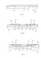
- FIG. 1Ais a cross section illustrating an integrated circuit according to some embodiments of the present invention.
- FIG. 1Bis a cross section illustrating a backplane arrangement including integrated circuits thereon according to some embodiments of the present invention
- FIG. 1Cis a cross section illustrating a backplane having integrated circuits according to some embodiments of the present invention.
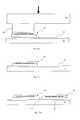
- FIG. 2is a cross section of a chiplet according to some embodiments of the present invention.
- FIGS. 3A-3Pare cross sections illustrating sequential stages in the fabrication and application of chiplets to a backplane according to some embodiments of the present invention
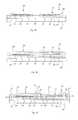
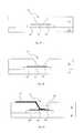
- FIGS. 4A-4Care cross sections illustrating misalignment of a chiplet having a large connection pad on a backplane
- FIGS. 5A-5Care cross sections illustrating misalignment of a chiplet having small connection pads on a backplane
- FIGS. 6A-6Care cross sections illustrating a chiplet on a backplane according to some embodiments of the present invention that addresses the misalignment illustrated in FIGS. 5A-5C ;
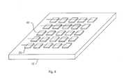
- FIG. 7is a perspective of a wafer having chiplets according to some embodiments of the present invention.
- FIG. 8is a perspective of a backplane having chiplets and wires according to some embodiments of the present invention.
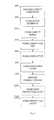
- FIG. 9is a flowchart illustrating methods of fabricating a chiplet according to some embodiments of the present invention.
- FIG. 10is a flowchart illustrating methods of fabricating integrated circuits on a source wafer according to some embodiments of the present invention.
- FIG. 11is a flowchart illustrating the formation of a backplane according to some embodiments of the present invention.
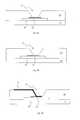
- FIGS. 12A and 12Bare cross sections illustrating the fabrication of a backplane according to some embodiments of the present invention.
- FIGS. 13A-13Dare cross sections illustrating the fabrication of a backplane according to further embodiments of the present invention.
- FIGS. 14A-14Care cross sections illustrating the fabrication of a backplane according to other embodiments of the present invention.
- FIG. 15is a cross section illustrating a protective bi-layer according to other embodiments of the present invention.
- first, second, etc.may be used herein to describe various elements, these elements should not be limited by these terms. These terms are only used to distinguish one element from another. For example, a first element could be termed a second element, and, similarly, a second element could be termed a first element, without departing from the scope of the present invention.
- relative termssuch as “lower” or “bottom” and “upper” or “top,” may be used herein to describe one element's relationship to another element as illustrated in the Figures. It will be understood that relative terms are intended to encompass different orientations of the device in addition to the orientation depicted in the Figures. For example, if the device in one of the figures is turned over, elements described as being on the “lower” side of other elements would then be oriented on “upper” sides of the other elements. The exemplary term “lower”, can therefore, encompasses both an orientation of “lower” and “upper,” depending of the particular orientation of the figure.
- Embodiments of the inventionare described herein with reference to cross-section illustrations that are schematic illustrations of idealized embodiments (and intermediate structures) of the invention. As such, variations from the shapes of the illustrations as a result, for example, of manufacturing techniques and/or tolerances, are to be expected. Thus, embodiments of the invention should not be construed as limited to the particular shapes of regions illustrated herein but are to include deviations in shapes that result, for example, from manufacturing. For example, an implanted region illustrated as a rectangle will, typically, have rounded or curved features and/or a gradient of implant concentration at its edges rather than a binary change from implanted to non-implanted region. Thus, the regions illustrated in the figures are schematic in nature and their shapes are not intended to illustrate the actual shape of a region of a device and are not intended to limit the scope of the invention.
- Some embodiments of the present inventionmay be used in the fabrication of advanced display backplanes, for example, by assembling thousands of tiny integrated circuits onto glass substrates using transfer-printing.
- circuitsonce circuits are printed onto a backplane or other target substrate, it may be necessary to form electrical interconnections.
- the printing processmay provide a high degree of accuracy, the chips may still be misplaced or misaligned on the order of 2-3 microns.
- interconnection processesmay need to take such possible misalignment into consideration.
- One interconnection approach towards addressing such misalignmentis to form contact pads in the circuits that are large enough to account for both the transfer-printing accuracy and also the misalignment and size of the via to be formed down to the metal pad.
- metal contact padswere relatively large, typically about 20 microns ⁇ 20 microns in size.
- a smaller contact padcan be formed in the circuit, for example, about 5 micrometers ( ⁇ m) ⁇ 5 ⁇ m, with a comparatively small via, for example, about 2 ⁇ m ⁇ 2 ⁇ m, formed above the metal contact.
- this processmay be performed during the fabrication of the integrated circuit wafer, so the related design rules may be of reduced importance.
- the metal contact padis reduced in size, and thus the design rules for the interconnection via to be formed on the large target substrate may be relaxed.
- Embodiments of the present inventionmay therefore provide improved electrical performance, fewer large-area photolithographic steps, improved yields, improved testability, increased density, and improved alignment tolerances for electrical circuit devices transferred from a source substrate to a destination substrate.
- an integrated circuitcomprises a chiplet substrate 55 having a surface 58 .
- Active elements 82 , 83 , 84are formed on or in the chiplet substrate 55 .
- the chiplet substrate 55can include an active layer 54 in which the active elements 82 , 83 , 84 can be formed.
- the active layer 54can include the entire chiplet substrate 55 or only a portion of the chiplet substrate 55 and can be doped or patterned to form the active elements 82 , 83 , 84 .
- the active elements 82 , 83 , 84can be integrated circuit elements.
- a connection pad 24is formed on the surface 58 of the chiplet substrate 55 .
- Chiplet wires 80electrically connect the active elements 82 , 83 , 84 and the connection pad 24 .
- Conductor elements 26 , 26 ′ that are electrically separate from the connection pad 24are formed on the surface 58 of the chiplet substrate 55 .
- the conductors 26 , 26 ′are spatially separated by a distance X from the connection pad 24 .
- the conductors 26 , 26 ′are electrically connected to a chiplet wire 80 or active element 82 , 83 , 84 .
- An insulating layer 28is formed over the surface 58 of the chiplet substrate 55 and over the conductor 26 , 26 ′ leaving at least a portion of the connection pad 24 exposed, for example through the chiplet via 32 formed in the insulating layer 28 .
- connection pad 24can be partially covered by the insulating layer 28 .
- the integrated circuitcan be a chiplet 20 .
- a “chiplet”may refer to a small integrated circuit that can be transferred to a backplane substrate 10 using a stamp as described below.
- two chiplets 20are located on the backplane 10 in desired design locations 21 and are covered with a planarization layer 30 .
- Backplane vias 33are formed in the planarization layer 30 in alignment with the connection pads 24 of the chiplets 20 .
- Backplane wires 40are formed in a single layer over the backplane 10 and insulating layer 28 and contact the connection pads 24 on the chiplets 20 .
- Backplane vias 33 and backplane wires 40are typically formed in separate masking steps from the location of the chiplets 20 and should be closely aligned with the chiplets 20 to ensure good electrical connections between the connection pads 24 and backplane wires 40 . In a practical system, however, it can be difficult to align the chiplets 20 with the backplane 10 and the backplane masks used to form backplane vias 33 and backplane wires 40 .
- two chiplets 20 ′, 20 ′′are located on the backplane 10 and are covered with a planarization layer 30 .
- the chiplet 20 ′is located in the design location 21 while, because of manufacturing tolerances, the chiplet 20 ′′ is mis-located or misaligned on the backplane 10 by a distance X (e.g., the same distance that is between the connection pad 24 and the conductor 26 ) away from the desired design location 21 ′.
- a backplane via 33is formed in the planarization layer 30 in alignment with the connection pads 24 of the chiplets 20 according to the desired design location 21 thereof.
- the backplane via 33may define an opening that is wider than the distance X between the connection pad 24 and the conductor 26 .
- Backplane wires 40are formed in a single layer over the backplane 10 and insulating layer 28 and contact the connection pads 24 on the chiplets 20 . In this example, the exposed portion of the connection pad 24 is smaller than the area of the backplane via 33 in plan view. Because the chiplet 20 ′′ is misaligned or otherwise not properly located relative to the desired design location 21 ′ on the backplane 10 , the backplane via 33 is not well aligned with the connection pad 24 on the chiplet 20 ′′, which is spaced a distance Y from the desired design location 21 ′ (where Y is greater than or equal to X). However, since the insulating layer 28 insulates the backplane wires 40 from the conductors 26 , the backplane wires 40 still provide a connection to the connection pads 24 and not to the conductors 26 .
- the chiplet substrate 55can be a semiconductor layer, for example silicon, GaAs, and/or other III-V compound semiconductors.
- the chiplet substrate 55can be crystalline, amorphous, polycrystalline, or microcrystalline and can have multiple patterned or unpatterned layers of different materials, including electrically insulating layers such as some oxides and nitrides, e.g. silicon dioxide and silicon nitride.
- the active layer 54can be a doped semiconductor or otherwise be processed to enable the formation of active elements 82 , 83 , 84 .
- the active elements 82 , 83 , 84can include electrical elements such as transistors, capacitors, resistors, and/or wires or electro-optical elements such as photo-sensors and/or light-emitting diodes, or both.
- the term “integrated circuit”may refer to a substrate that has been processed to form circuits integrated into a substrate, for example by photo-lithographic processes, to form optical, electrical, or electro-optic circuits that transform, process, and/or conduct electrical or optical energy.
- a “chiplet”can refer to a small integrated circuit, for example an integrated circuit that may be too small to be packaged and used in an electrical circuit using conventional pick-and place, surface mount, or flip-chip methods.
- chiplets as described hereincan have substrates that are 5-10 microns thick, 10-20 microns thick, 20-50 microns thick, or 50-100 microns thick. Chiplets can be 10-100 microns wide and 20-500 microns long, for example.
- the chipletscan have different sizes or areas, for example, 1000 square microns or 10,000 square microns, 100,000 square microns, or 1 square mm, or larger, and can have variable aspect ratios, for example 2:1, 5:1, or 10:1.
- chipletshould not be used for purposes of limitation, but may be used to distinguish integrated circuit elements of different sizes from one another.
- the active elements described hereincan be constructed in a source wafer using conventional photo-lithographic processes.
- the source wafercan be a crystalline semiconductor with very good electrical performance.
- the chiplet wires 80can be made of metal, for example aluminum, in layers, for example metal layer 1 , metal layer 2 , metal layer 3 , and so forth, as is done in the integrated circuit design and layout arts.
- the chiplet wires 80 in the various layersare used to electrically interconnect the active elements 82 , 83 , 84 to form electrical circuits.
- the top metal layercan be formed on the surface 58 of the chiplet substrate 55 to provide a connection pad 24 to which control or power signals external to the chiplet 20 can be electrically connected.
- the conductor 26can be formed from a same layer and in a common processing step with the connection pad 24 , for example a patterned metal layer.
- the conductor element 26can be a metal interconnect such as a chiplet wire 80 or can be or include an active element 82 , 83 , 84 or a portion of an active element 82 , 83 , 84 .
- the conductor 26conducts or otherwise controls electrical current and is isolated from the connection pad 24 so that the conductor 26 and connection pads 24 are electrically separate and distinct.
- the conductor 26can be a connection pad separate from connection pad 24 .
- a patterned insulating layercan be located in a layer beneath the conductors 26 , 26 ′ and connection pad 24 and semiconductor layers in the active layer 54 to reduce and/or prevent unwanted electrical conduction.
- the insulating layer 28is located at least partly over the conductors 26 , 26 ′ and connection pad 24 and is electrically insulating.
- the insulating layer 28can be made of a variety of materials and perform multiple functions.
- the insulating layer 28can be, for example a passivation or planarization layer and can comprise, for example, an oxide layer, a nitride layer, and/or a polymer layer, such as a resin (for example a curable resin).
- the insulating layer 28does not necessarily cover the entire chiplet substrate 55 , active layer 54 , and conductors 26 , 26 ′, but covers at least a portion of each of the chiplet substrate 55 , active layer 54 , and conductors 26 , 26 ′.
- connection pad 24can be formed of patterned metal, for example aluminum, silver, titanium, tungsten, metal alloys, and/or layers of metals.
- the connection pad 24can be exposed through the insulating layer 28 by forming a via 32 through the insulating layer 28 .
- Viascan be formed by coating a photo-curable resin over the surface, pattern-wise curing the resin to define the via, and then etching the resin and the insulating layer 28 beneath the resin to form the via 32 and removing the resin. Methods of coating photo-curable resins, pattern-wise exposing (e.g. with ultra-violet light though a mask) and pattern-etching the resin and layers beneath the resin to form vias are used in the art.
- the coated resincan form the insulating layer 28 and/or a portion thereof Referring to FIG. 2 , the via 32 can have a larger area at the side of the insulating layer 28 opposite the chiplet substrate 55 (having a linear dimension 39 ) than the area on the connection pad 24 (having a linear dimension 38 ). In other words, the via 32 may narrow as it extends through the insulating layer 28 .
- connection pads 24it may be desirable to reduce the size or surface area the connection pads 24 so that other areas of the surface 58 of the chiplet substrate 55 and active layer 54 can be used for routing wires to other active elements 82 , 83 , 84 with conductors 26 independently of the connection pad 24 . To enable this, the conductor 26 is not directly electrically connected to the connection pad 24 . As illustrated in FIG.
- conductor 26 ′directly electrically connects active element 84 to active element 83 and is electrically isolated from the connection pad 24 .
- Two elementsare directly electrically connected when a single electrically conductive wire contacts both elements so that electrical current can flow directly from one element to the other without passing through any other intervening elements, such as electrically controlling or processing elements.
- chiplets of the present inventionwhen located over or printed on a backplane, chiplets of the present invention provide high-performance electrical or optical devices that can be electrically connected using lower-resolution, and thus lower-cost, wiring methods and materials.
- the backplanecan include heterogeneous components distributed over the backplane, either regularly or irregularly.
- Backplane substratescan be glass, polymer, metal, and/or semiconductor, for example silicon, GaAs, or other III-V materials.
- the chipletscan respond to external controllers located on the backplane and/or externally to the backplane.
- the backplane of the present inventioncan be used, for example, to form an active-matrix backplane where the chiplets are organized into an array controlling a corresponding array of elements, for example pixels in a display or a digital radiographic plate.
- the chipletscan be light-emitters, for example light-emitting diodes or LEDs, or a vertical cavity side-emission laser (e.g. edge laser).
- the chipletscan serve to convert incident light into electricity, forming a photovoltaic device, for example with photo-diodes.
- the contacts or any metal layers formed beneath the active layercan reflect incident light that passes through the active component back through the active component. In cases where a chiplet serves to convert light to electrical current, this reflection can allow for improved absorption of light by the chiplet. In the case where the chiplet emits light, or controls the emission of light by other layers, the reflection can provide improved emission of light.
- a backplaneaccording to some embodiments of the present invention can be constructed as described below.
- a source substrate 50for example a wafer, has a sacrificial layer 52 formed thereon.
- the sacrificial layer 52can be, for example, an oxide such as silicon dioxide and can be deposited by sputtering.
- a chiplet substrate 55is formed over the sacrificial layer 52 and can also be deposited by sputtering.
- Active layer 54can be formed by pattern-wise doping the chiplet substrate 55 .
- the chiplet substrate 55is processed to form active elements in the active layer 54 .
- the chiplet substrate 55 and active layer 54serve as the substrate of a small integrated circuit and can include additional layers and materials and can be annealed or otherwise processed to improve its characteristics, for example electron mobility.
- Active elements 82FIG. 1
- the active layer 54can include metal interconnect layers, doped material layers, and/or other layers used in the integrated circuit arts for forming active elements, such as electrical or electro-optic elements, e.g. transistors, photo-sensors, photo-voltaic elements, light-emitting diodes, etc.
- connection pads 24 and conductors 26are formed on the surface (element 58 in FIG. 1 ) of the source substrate 50 and electrically connect the active elements in the active layer 54 .
- the conductors 26are not directly electrically connected to the connection pad 24 .
- multiple connection pads 24 and conductors 26are formed on a single chiplet.
- the connection pads 24can be spatially separated from each other and the conductors 26 can be located between connection pads 24 in some embodiments.
- Each set of active elements, connection pads 24 , and conductors 26form an integrated circuit chiplet 20 .
- connection pads 24 and conductors 26are formed, the substrate surface, connection pads 24 , and conductors 26 are coated with an insulating layer 28 .
- the insulating layer 28is electrically insulating and can comprise a variety of suitable materials, for example planarizing or passivation layers made of insulating material such as silicon oxides, silicon nitrides, and/or polymer resins.
- the insulating layercan be deposited by a variety of methods, for example by sputtering, spin coating, or curtain coating.
- the insulating layer 28can be patterned to expose at least a portion of the connection pad 24 and to cover over at least a portion of a conductor 26 .
- the insulating layer 28covers all, or most of, the conductor 26 , as shown in FIG. 3D .
- the insulating layer 28can also be patterned to expose the active layer 54 or chiplet substrate 55 between integrated circuit chiplets 20 .
- Each wafer substrate 50can have a plurality of integrated circuit chiplets 20 formed thereon.
- wafer-scale testingcan be applied at this stage. While conventional testing probes could be applied to the chiplet structures shown in FIG. 3B , the smaller connection pads are more difficult to contact with an electrical probe and a probe directed to one connection pad 24 can be shorted to neighboring connection pads 26 . In contrast, when applied to the structure of FIG. 3D , an electrical probe directed to connection pad 24 cannot be shorted to other connection pads 26 due to the presence of the insulating layer 28 .
- a protective layer 29is formed over the insulating layer 28 and connection pads 24 .
- the protective layer 29can be deposited by maskless sputtering or coating.
- the protective layer 29can be amorphous silicon in some embodiments; however, amorphous silicon can have undesirable interactions with the conductive materials that may be used in the connection pads, such as metals and, particularly, aluminum. Therefore, in some embodiments of the present invention as illustrated in FIG. 15 , the protective layer 29 can be a bi-layer 29 A and 29 B having different material in each layer of the bi-layer.
- Layer 29 Acan be selected and/or optimized to protect the connection pad material, for example silicon dioxide, while layer 29 B compatible with layer 29 A, for example amorphous silicon, can be selected and/or optimized for protection against subsequent processing steps described below, such as etching with hydrofluoric acid. Since both layers 29 A and 29 B are blanket coated, they can be deposited and removed (e.g. by sputtering and then etching) without further patterning process steps. Hence, the use of an additional protective layer can improve process compatibility with the release process used to fabricate printable chiplets described below.
- Trenches 34are formed, as shown in FIG. 3F and also in the top view of FIG. 7 , between and around each chiplet 20 through the active layer 54 to expose the sacrificial layer 52 , leaving tethers 35 ( FIG. 7 ) attaching the chiplets 20 to anchors 36 that form areas attached to the source substrate 50 .
- the anchors 36can be areas over the source substrate 50 and above the sacrificial layer 52 between the chiplets 20 .
- the trenches 34define and separate the chiplets 20 from each other and from the anchors 36 .
- the anchors 36can include active elements and test pads (not shown) accessible to external test probes, and a plurality of electrically conductive tethers 35 .
- Each anchoris located over and in contact with the patterned sacrificial layer 52 , 52 ′, and has a tether 35 connecting the anchor 36 to an integrated circuit chiplet 20 .
- the tethers 35electrically connect active elements in the integrated circuit chiplet 20 to one or more exposed electrical test pads formed in the anchor 36 .
- the bi-layer of FIG. 15can be formed in two separate steps and may involve a different etching process.
- the first stepdeposition of layer 29 A
- the trenches 34can be etched through one or more, but not all, of the layers above the sacrificial layer 52 .
- the second protective layer29 B
- the protective layers and etchantscan be separately selected and/or optimized to provide improved results, for example better yields.
- the sacrificial layer 52is removed from beneath the chiplets 20 , leaving an open location or void 52 ′ (where the sacrificial layer was) such that the chiplets 20 are suspended by the tethers 35 ( FIG. 7 ) over the source substrate 50 .
- the anchors 36are not separated from the source substrate 50 by the etching (e.g., the sacrificial layer 52 remains beneath the anchors 36 ), so that the chiplets 20 are still connected (through the tethers 35 and anchors 36 ) to the source substrate 50 .
- the anchors 36are shown smaller than the chiplets 20 for clarity; in practice the anchors 36 can be larger in at least one dimension than the chiplets 20 so that the chiplets 20 can be released by etching from the source substrate 50 before the anchors 36 are released. For example, by stopping the etching process at an appropriate time, the chiplets 20 can be released while the anchors 36 are not released.
- FIG. 3Gcorresponds to the cross section indicated by A-A′ in FIG. 7 .
- Patterned etching of insulation layers, forming trenches in active layers and active element layers, and removing sacrificial layersare process steps used in semiconductor device fabrication.
- the active layer 54can be crystalline silicon and the sacrificial layer 52 can be an oxide, such as silicon dioxide.
- the sacrificial layer 52can be etched with hydrofluoric acid.
- the protective layer 29protects the other elements from chemical attack by the etchants used to form the trenches 34 and remove the sacrificial layer 52 .
- the protective layercan be, for example amorphous silicon, and can be blanket coated over the chiplets to protect the chiplet elements against attack by etchants such as hydrofluoric acid.
- the protective layer 29can be removed, again without requiring a mask step, as shown in FIG. 3H .
- electrical testingcan be performed, in addition to or rather than at the earlier stage before the protective layer 29 is applied at the step illustrated in FIG. 3E , as noted above. In other embodiments, the protective layer 29 can be removed at a later process step, as described below.
- the chiplets and the processes described hereincan include additional layers and process steps. Furthermore, the process steps can be performed in various different orders, depending on the materials and process capabilities. For example, the insulating layer etch that exposes the connection pad (shown in FIG. 3D ) can be performed after the trench formation and sacrificial layer exposure, or after the removal of the sacrificial layer.
- a stamp 60for example an elastomeric or PDMS stamp, having protrusions shaped and sized to match the chiplets 20 can be pressed against the chiplets 20 , breaking the tethers and adhering the chiplets 20 to the stamp 60 as the stamp 60 is removed ( FIG. 3J ). Not every chiplet 20 need be removed from the source substrate 50 , and the stamping process can be repeated one or multiple times with different chiplets applied to different locations on the backplane substrate.
- the adhered chiplets 20 on the stamp 60are pressed against a destination backplane 10 ( FIG. 3K ) including an adhesive layer 72 to adhere the chiplets 20 to the backplane 10 .
- the backplane 10provides a target or receiving substrate on which an active device can be constructed.
- the adhesive layer 72can cover only a relatively small portion of the backplane 10 so that patterned wires can be formed largely on the backplane 10 , or the adhesive layer 72 can extend over much of the backplane 10 so that any patterned wires are formed largely on the adhesive layer 72 .
- the stamp 60can be removed and the adhesive layer 72 cured. ( FIG. 3L ). As shown in FIG. 3M , the stamping process can be repeated to locate multiple chiplets over the backplane 10 in multiple locations.
- a sparse array of chipletscan be adhered to the backplane 10 .
- a chiplet 20 ′′can be mis-located or misaligned with respect to a desired design location 21 ′.
- the mis-location or misalignmentcan be random or have a random distribution and can differ from one chiplet to another so that the relative locations of the chiplets differ with respect to the desired design locations.
- the protective layer ( 29 in FIG. 3G )can be removed at this step rather than at the step corresponding to FIG. 3H in some embodiments. Removing the protective layer at this point in the process allows the protective layer to protect the chiplets through the stamping process ( FIGS. 3I-3K ). As noted above, the removal of the protective layer can be a maskless process.
- a planarization layer 30is coated over the backplane 10 and chiplets 20 ′, 20 ′′.
- the coatingcan be local to each chiplet 20 ′, 20 ′′ or can be uniformly coated over the backplane 10 .
- the planarization layer 30is then processed to form a backplane via 33 ′′ over at least a portion of the exposed connection pad 24 associated with chiplet 20 ′′ and a backplane via 33 ′ over at least a portion of the exposed connection pad 24 associated with chiplet 20 ′.
- An etchant used to form the backplane vias 33 ′′may be selective to the insulating layer 28 .
- the protective layer29 in FIG.
- FIGS. 3Gcan then be removed at this step rather than at FIG. 3H .
- Removing the protective layer at this point in the processallows the protective layer to protect the chiplets through the stamping and planarization process ( FIGS. 3I-3N ).
- the removal of the protective layercan be a maskless process, although in this case the protective layer may only be removed in the via area since the planarization layer 30 covers the remainder of the chiplet area (see FIGS. 13A-13C and FIGS. 14A-14C discussed below).
- the via 33 ′′is misaligned with respect to the chiplet 20 ′′ so that the via 33 ′′ exposes a portion (e.g., less than an entirety) of the connection pad 24 and chiplet via 32 and exposes at least a portion of the insulating layer 28 .
- a misalignmentcan occur by mis-locating or misaligning the chiplet 20 ′′ on the backplane 10 , the backplane 10 , or by mis-locating or misaligning the process elements, e.g. masks, used to form the via 33 ′′ or to form a backplane interconnection. Note that the misalignment is between the location of the chiplet connection pad and any connecting backplane elements.
- Chiplet 20 ′ and backplane via 33 ′are properly aligned.
- a backplane wire 40is formed over the planarization layer 30 in contact with the connection pads 24 in the backplane vias 33 ′′ and 33 ′. Because the insulating layer 28 is formed over the conductors 26 , the backplane wire 40 does not electrically connect the connection pad 24 to the conductors 26 , and does not, therefore, electrically short the connection pad 24 and conductor 26 .
- the planarization layer 30can comprise, for example, a curable resin, and can be patterned to form a via using photo-sensitive resins, masks, and light exposure through the masks. In embodiments illustrated in FIG. 12A , the planarization layer 30 can be removed from the surface of the chiplet 20 exposing the integrated circuit chiplet and the backplane wires formed directly on the chiplet 20 and insulating layer 28 ( FIG. 12B ).
- the chiplet 20is blanket coated with a protective layer 29 (for example a passivation layer) before it is removed from the wafer source substrate.
- a protective layer 29for example a passivation layer
- the chipletis then located on the backplane 10 ( FIG. 13B ) and coated with planarization layer 30 , and a backplane via 33 formed in the planarization layer 30 ( FIG. 13C ) and the protective layer 29 removed ( FIG. 13D ) in the via 33 before the formation of any interconnections.
- the protective layer 29 removaldoes not require patterning and can be performed after the planarization layer is processed.
- FIGS. 14A-14Cthe process illustrated in FIGS. 12A and 12B can also be employed with the blanket-coated protection layer of FIGS. 13A-13D .
- the entire protective layer 29is removed from the surface of the chiplet 20 .
- the chiplets 20 on the backplane 10have a protective layer 29 (formed as in FIG. 13A ) and the backplane 10 has a blanket-coated planarization layer (as in FIG. 13B ).
- the planarization layer 30is removed to below the surface of the chiplet 20 (as in FIG. 12A ) exposing the protective layer 29 .
- the protective layer 29is then removed from the surface of the chiplet 20 and the chiplet via 32 and the insulating layer 28 are exposed.
- the steps of reducing the planarization layer 30 and removing the protective layer 29are maskless.
- the only process step after the chiplet construction that requires a maskis the formation of the chiplet via 32 on the wafer source substrate.
- no mask step at allmay be required for backplane processing if the etching process is carefully controlled to expose the connection pads.
- Metal interconnects, such as those of FIG. 12Bcan then be formed using either masked patterning or micro-deposition (such as inkjet) of conductive material.
- embodiments of the present inventionenable backplane interconnection methods that require fewer large-area photolithographic processes, particularly patterning processes.
- FIGS. 12A-B , 13 B-D, and 14 A-Cshow only a single chiplet 20 on the backplane 10 .
- the present inventionincludes backplanes having two or more chiplets 20 thereon.
- the backplane of the present inventionincludes an array of chiplets 20 as illustrated in FIG. 8 .
- the present inventioncan provide a chiplet structure that is robust in the presence of manufacturing process faults that may create relative mis-alignments between features on a chiplet and features on the backplane, even when using relatively small features on the chiplet, e.g. the connection pad.
- the small featurescan provide additional space within the chiplets for active elements or wiring, thereby increasing the functionality of the chiplets an enabling improved electrical performance.
- embodiments of the present inventioncan enable smaller connection pads that do not require as much space on a chiplet substrate surface. Therefore, chiplets can have a greater functionality or, alternatively, smaller chiplets can be employed.
- chiplet location tolerances of 10 micronscan be used, whereas, conventional tolerances can be 5 microns, 2 microns, or 1 micron.
- interconnection methods that have greater margins of errorcan be applied to transfer-printed substrates.
- embodiments of the present inventioncan provide higher manufacturing yields and lower costs in the presence of manufacturing variability and can employ lower-cost tools to manufacture backplanes.
- Embodiments of the present inventioncan provide advantages of improved electrical performance and density in integrated circuits transfer-printed over large substrates. Aspects of the invention can also reduce the number of large-area photolithographic steps, reduce alignment tolerance requirements, and are compatible with wafer testing and high-yield release processes for the transfer-printed integrated circuits.
- a chiplet 20 with a relatively large connection pad 22is located on a backplane 10 with a planarizing layer 30 and corresponding backplane via 33 .
- a wire formed over the planarizing layer 30can contact the large connection pad 22 . If the backplane via 33 is not properly aligned with the chiplet 20 large connection pad 22 , as shown in FIG.
- a wire formed over the planarizing layer 30can still contact the large connection pad 22 without difficulty because the surface of the large connection pad 22 extends far enough along the chiplet 20 surface to compensate for some relative mis-alignment between the backplane 10 and the chiplet 20 .
- a backplane wire 40 formed over the planarizing layer 30can still contact the large connection pad 22 , as shown in FIG. 4C .
- the large connection pad 22occupies a relatively large amount of space on the surface of the chiplet 20 , thereby reducing the potential functionality of the chiplet.
- a chiplet 20 with a relatively small connection pad 24 and relatively small conductors 26are located on a backplane 10 with a planarizing layer 30 and corresponding backplane via 33 . Because smaller connection pads and conductors are used, compared to those in FIGS. 4A-4C , the chiplet 20 can have increased functionality by employing the space otherwise used by a large connection pad for additional circuitry and circuit connections. As shown in FIG. 5A , if the backplane via 33 is properly aligned with the chiplet 20 small connection pad 24 , a wire formed over the planarizing layer 30 can contact the small connection pad 24 without difficulty.
- a wire formed over the planarizing layer 30can contact not only the small connection pad 24 but also the conductor 26 .
- a backplane wire 40 formed over the planarizing layer 30can form an electrical short circuit 42 between the small connection pad 24 and the conductor 26 , as shown in FIG. 5C .
- a chiplet 20 with a small connection pad 24 , small conductors 26 , insulating layer 28 , and chiplet via 32is located on a backplane 10 having a planarizing layer 30 and corresponding backplane via 33 .
- a wire formed over the planarizing layer 33can contact the small connection pad 24 without difficulty.
- the backplane via 33can expose at least a portion of the connection pad 24 and the insulating layer 28 over the conductor 26 .
- a backplane wire 40 formed over the planarizing layer 30therefore contacts only the small connection pad 24 and does not contact the conductor 26 because of the insulating layer 28 , as shown in FIG. 6C .
- a wire that electrically connects a chiplet mis-aligned with respect to the backplane 10does not cause short circuits on the chiplet surface and still allows the use of space-conserving small connection pads 24 and additional, high-density conductors 26 for interconnecting active elements in the integrated circuit chiplet 20 .
- connection pads 24 on a single chiplet 20can be spaced apart from one another as far as is practical so that any mis-alignment between the chiplet 20 and backplane 10 will not result in short circuits between two connection pads 24 on the same chiplet 20 .
- each of the connection pads 24will have an exposed portion, connection pads 24 that are too close together can be short circuited by wires 40 . Therefore, in some embodiments, one or more of the conductors 26 may be arranged between adjacent connection pads 24 to separate the connection pads 24 so far as is practical.
- an integrated circuitcan be made by providing a chiplet substrate in step 200 , forming active elements on or in the chiplet substrate in step 205 , forming chiplet wires electrically connecting the active elements and the connection pad in step 210 , forming a connection pad on a surface of the chiplet substrate in step 215 , forming one or more conductors electrically separate from the connection pad on the surface of the chiplet substrate in step 220 , the conductors electrically connected to a chiplet wire or active element, and forming an insulating layer over the chiplet substrate and the conductor in step 225 , leaving at least a portion of the connection pad exposed.
- connection padcan be exposed with vias by photo-lithographically patterned etching of the insulating layer to pattern-wise expose the connection pad in step 230 .
- An optional first protective layer(as discussed with reference to FIG. 15 ) can be formed over the insulating layer and the exposed connection pads in step 235 .
- a wafer having integrated circuitscan be made by providing a wafer substrate in step 300 , forming a sacrificial layer over the wafer substrate in step 305 , forming an active layer over the sacrificial layer in step 310 , and forming a plurality of integrated circuits on or in the active layer in step 315 .
- Each integrated circuitcan include active elements formed on or in the active layer, a connection pad formed on a surface of the active layer, chiplet wires electrically connecting the active elements and the connection pad, a conductor electrically separate from the connection pad formed on the surface of the active layer and electrically connected to a chiplet wire or active element, and an insulating layer formed over the active layer and the conductor, leaving at least a portion of the connection pad exposed.
- the integrated circuit chipletscan be made according to the methods described in FIG. 9 .
- the integrated circuitscan be released from the wafer as described in FIGS. 3A-3O in step 320 and the protective layer, if formed in step 235 ( FIG. 9 ), can be removed in step 325 .
- a method of making a backplane having integrated circuitsincludes the steps of providing a backplane substrate in step 400 and providing a plurality of integrated circuits located on the backplane in step 405 .
- the integrated circuitscan be located on the backplane in step 410 , for example, using a transfer printing process.
- Each integrated circuitcan include a chiplet substrate, active elements formed on or in the chiplet substrate, a connection pad formed on a surface of the chiplet substrate, chiplet wires electrically connecting the active elements and the connection pad, a conductor electrically separate from the connection pad formed on the surface of the chiplet substrate and electrically connected to a chiplet wire or active element, and an insulating layer formed over the chiplet substrate and the conductor, leaving at least a portion of the connection pad exposed.
- the integrated circuit chipletscan be made according to the methods described in FIG. 9 in some embodiments.
- a protective layercan optionally be formed over the insulating layer and exposed connection pad in step 235 . If the protective layer was formed (step 235 FIG. 9 ) and not removed in step 325 ( FIG. 10 ), it can be removed in step 415 before electrical connections are made in a single layer to the connection pads in step 420 .
- a structured substrate having transferrable integrated circuit chipletsincludes a substrate 50 , a patterned sacrificial layer 52 , 52 ′ formed on the substrate 50 , and a plurality of integrated circuit chiplets 20 formed on the patterned sacrificial layer 52 , 52 ′.
- Each integrated circuit chiplet 20includes a separate chiplet substrate 55 having a surface, where the separate chiplet substrate 55 detached from the substrate 50 by the pattern of the sacrificial layer 52 , 52 ′.
- Active elementsare formed on or in the chiplet substrate 55 , a connection pad 24 is formed on the surface of the chiplet substrate 55 , and chiplet wires are formed on or in the chiplet substrate 55 electrically connecting the active elements and the connection pad 24 .
- a conductor 26 electrically separate from the connection pad 24is formed on the surface of the chiplet substrate 55 , where the conductor 26 electrically connected to a chiplet wire or active element.
- a patterned insulating layer 28is formed over the chiplet substrate 55 and the conductor 26 , leaving at least a portion of the connection pad exposed 24 .
- a method of fabricating a structured substrate having transferrable integrated circuit chipletsincludes the steps of providing a substrate, forming a sacrificial layer on the substrate, forming a chiplet substrate layer on the sacrificial layer, the chiplet substrate layer having a surface, forming active elements on or in the chiplet substrate layer, forming a connection pad on the surface, forming chiplet wires on or in the chiplet substrate electrically connecting the active elements and the connection pad, forming a conductor electrically separate from the connection pad on the surface, the conductor electrically connected to a chiplet wire or active element, forming an insulating layer over the chiplet substrate and the conductor, leaving at least a portion of the connection pad exposed, and patterning the chiplet substrate layer and the sacrificial layer to form separate chiplet substrates detached from the substrate.
- Embodiments of the present inventioncan be used in transferring chiplets made with crystalline semiconductor materials that have much higher performance than thin-film active components. Furthermore, the flatness, smoothness, chemical stability, and heat stability requirements for a backplane substrate used in embodiments of the present invention can be greatly reduced because the adhesion and transfer process is not significantly limited by the backplane substrate material properties. Manufacturing and material costs can also reduced because of higher utilization rates of expensive materials (e.g. the active substrate) and reduced material and processing requirements for the backplane substrate. Embodiments of the present invention can also provide improved circuit density in small integrated circuits while reducing alignment and tolerance requirements for chiplets placed on a backplane. Thus, performance can be increased and costs can be reduced for active integrated circuits distributed over backplanes.
- embodiments of the present inventioncan provide a reduction in masking steps on the backplane improving yields and reducing costs, can provide reduced connection pad size improving device functionality, and can provide less stringent tolerance requirements thereby improving yields and reducing processing costs.
Landscapes
- Engineering & Computer Science (AREA)
- Computer Hardware Design (AREA)
- Microelectronics & Electronic Packaging (AREA)
- Power Engineering (AREA)
- Physics & Mathematics (AREA)
- Condensed Matter Physics & Semiconductors (AREA)
- General Physics & Mathematics (AREA)
- Manufacturing & Machinery (AREA)
- Internal Circuitry In Semiconductor Integrated Circuit Devices (AREA)
- Semiconductor Integrated Circuits (AREA)
Abstract
Description
- This application claims priority under 35 U.S.C. §119(e) from U.S. Provisional Patent Application Ser. No. 61/416,527 entitled “Interconnection Structure and Method for Transfer-Printed Integrated Circuits,” filed with the United States Patent and Trademark Office on Nov. 23, 2010, the disclosure of which is incorporated by reference herein in its entirety.
- The present invention relates to integrated circuit device fabrication, and more particularly, to apparatus and methods for assembling integrated circuit elements on a substrate.
- Large substrates with electronically active components distributed over the extent of the substrate are used in a variety of electronic systems, for example imaging devices such as flat-panel liquid crystal or OLED display devices and in digital radiographic plates. Large substrates with electrically active components are also found in flat-panel solar cells.
- The electronically active components on flat-panel substrates are typically formed by sputtering a layer of inorganic semiconductor material or by spin-coating a layer of organic semiconductor material over the entire substrate and processing the layer to form electronic components. However, such coatings typically may have relatively poor electronic characteristics. Inorganic semiconductor materials can be processed to improve their electronic characteristics; for example, amorphous silicon can be heat-treated to form polycrystalline silicon. In other processes, microcrystalline semiconductor layers can be formed by using an underlying seeding layer. These methods typically improve the electron mobility of the semiconductor, but the performance of the resulting layer may still be worse than is often desired or needed.
- The substrate and layer of semiconductor material can be photo-lithographically processed to define electronically active components, such as transistors. Such transistors are known as thin-film transistors (TFTs) since they are formed in a thin layer of semiconductor material, typically silicon. The photo-lithographic processing typically requires high-resolution mask steps to pattern the semiconductor materials and metal interconnections on the substrate. In these devices, the substrate is often made of glass, for example, Corning Eagle® or Jade® glass designed for display applications.
- However, these conventional thin-film techniques may have limitations. Despite processing methods used to improve the performance of thin-film transistors, such transistors may have a performance lower than the performance of conventional integrated circuits formed in mono-crystalline semiconductor material. Also, semiconductor material and active components may be used on only portions of the substrate, leading to wasted material and increased material and processing costs. The substrate materials may be limited by the processing steps that may be necessary to process the semiconductor material, as well as the photo-lithographic steps used to pattern the active components. For example, plastic substrates have a limited chemical and heat tolerance and typically do not readily survive photo-lithographic processing. Furthermore, the manufacturing equipment used to process large substrates with thin-film circuitry may require relatively high resolution and may be expensive.
- In another manufacturing technique, a mono-crystalline semiconductor wafer may be employed as the substrate. While this approach can provide substrates with similar performance as integrated circuits, the size of such substrates may be limited, for example, to a 12-inch diameter circle, and the wafers are relatively expensive compared to other substrate materials such as glass or polymer.
- In yet another approach, thin layers of semiconductor may be bonded to a substrate and then processed. Such a method is known as semiconductor-on-glass or silicon-on-glass (SOG) and is described, for example, in U.S. Patent Application Publication No. 2008/0224254, published Sep. 18, 2008. If the semiconductor material is crystalline, high-performance thin-film circuits can be obtained. However, the bonding technique can be expensive and the high-resolution processing equipment needed to form thin-film active components on large substrates may be expensive.
- It is also known to provide relatively large integrated circuits in surface mountable packages that are directly adhered to a substrate. However, these integrated circuits are relatively large and additional layers may not be easily formed over the integrated circuits. Furthermore, electrical inter-connections to the surface-mountable package may require high-resolution patterning.
- Publication number 11-142878 of the Patent Abstracts of Japan entitled “Formation of Display Transistor Array Panel” describes etching a substrate to remove it from a thin-film transistor array on which the TFT array was formed. TFT circuits formed on a first substrate can be transferred to a second substrate by adhering the first substrate and the TFTs to the surface of the second substrate and then etching away the first substrate, leaving the TFTs bonded to the second substrate. This method typically requires etching a significant quantity of material and risks damaging the exposed TFT array. Also, as with the other techniques discussed above, the patterned processing may require expensive, high-resolution equipment.
- Another method of locating material on a substrate is described in U.S. Pat. No. 7,127,810. In this method, a first substrate carries a thin-film object to be transferred to a second substrate. An adhesive is applied to the object to be transferred or to the second substrate in the desired location of the object. The substrates are aligned and brought into contact. A laser beam irradiates the object to abrade the transferring thin film so that the transferring thin film adheres to the second substrate. The first and second substrates are separated, peeling the film in the abraded areas from the first substrate and transferring it to the second substrate. In one embodiment, a plurality of objects may be selectively transferred by employing a plurality of laser beams to abrade selected areas. Objects to be transferred can include thin-film circuits. Further processing, for example to provide electrical interconnections between the transferred objects, may require high-resolution processing.
- U.S. Pat. No. 6,969,624 describes a method of transferring a device from a first substrate onto a holding substrate by selectively irradiating an interface with an energy beam. The interface is located between a device for transfer and the first substrate and includes a material that generates ablation upon irradiation, thereby releasing the device from the substrate. For example, a light-emitting device (LED) can be made of a nitride semiconductor on a sapphire substrate. The energy beam is directed to the interface between the sapphire substrate and the LED nitride semiconductor releasing the LED and allowing the LED to adhere to a holding substrate coated with an adhesive. The adhesive is then cured. These methods, however, may require the patterned deposition of adhesive on the object(s) or on the second substrate. Moreover, the laser beam that irradiates the object may be shaped to match the shape of the object and the laser abrasion can damage the object to be transferred. Furthermore, the adhesive cure takes time, which may reduce the throughput of the manufacturing system. Further processing, for example to provide electrical interconnections between the transferred objects, may also require high-resolution processing.
- In another method for transferring active components from one substrate to another, described in “AMOLED Displays using Transfer-Printed Integrated Circuits” published in the Proceedings of the 2009 Society for Information Display International Symposium Jun. 2-5, 2009, in San Antonio, Tex., US, vol. 40, Book 2, ISSN 0009-0966X, paper 63.2 p. 947, small integrated circuits (chiplets) with connection pads formed on the chiplet surface are formed in a wafer and released from the wafer by etching beneath the circuits. A PDMS stamp is pressed against the wafer and the circuits adhered to the stamp. The circuits are then pressed against a substrate coated with an adhesive, adhered to the substrate, and the adhesive is subsequently cured. Subsequent photo-lithographic processes are used to form electrical wires over the substrate and on to the connection pads. However, the position and orientation of the chiplets resulting from the printing process can vary somewhat. Thus, the connection pads may need to be relatively large so that the wires formed by the photo-lithographic processing steps contact the contact pads. The relatively large connection pads can reduce the space available for circuits and circuit connections, and thus can reduce the functionality of the chiplets.
- According to some embodiments of the present invention, integrated circuit elements are provided on a receiving substrate. Each of the integrated circuit elements includes a chiplet substrate having a connection pad and a conductor element on a surface thereof, where the connection pad and the conductor element are electrically separated. At least one of the integrated circuit elements is misaligned on the receiving substrate relative to a desired position thereon such that the at least one of the integrated circuit elements is positioned on the receiving substrate at a distance from the desired position that is greater than or equal to a distance between the conductor element and the connection pad. A conductive layer is formed on the receiving substrate including the integrated circuit elements thereon such that the connection pad of each of the integrated circuit elements is electrically connected to the conductive layer.
- In some embodiments, each of the integrated circuit elements may include an insulating layer on the chiplet substrate that exposes at least a portion of the connection pad to the conductive layer and covers the conductor element on the surface of each chiplet substrate to electrically separate or isolate the conductor element from the conductive layer.
- In some embodiments, a planarization layer may be formed on the receiving substrate including the integrated circuit elements thereon. The planarization layer may include via openings therein, where respective positions of the via openings in the planarization layer may be based on respective desired positions of the integrated circuit elements on the receiving substrate. The conductive layer may be formed on the planarization layer and in the via openings to electrically contact the connection pad of each of the integrated circuit elements.
- In some embodiments, at least one of the via openings has a diameter or other dimension sufficient to expose a portion of the connection pad and a portion of the insulating layer covering the conductor element of the at least one of the integrated circuit elements that is misaligned on the receiving substrate. For example, the dimension of the at least one of the via openings may be greater than the distance between the conductor element and the connection pad on the surface of the chiplet substrate.
- In some embodiments, the connection pad of each of the integrated circuit elements may be coupled to an active element therein such that the conductive layer provides an electrical connection between respective active elements of each chiplet substrate, and the conductor element of each of the integrated circuit elements may provide an electrical connection between respective active elements of a same chiplet substrate.
- In some embodiments, each chiplet substrate may include a plurality of connection pads and a plurality of conductor elements, and at least one of the conductor elements may be provided between adjacent ones of the connection pads on the surface of each chiplet substrate.
- In some embodiments, the integrated circuit elements including a plurality of active elements therein may be formed on a source substrate. The integrated circuit elements may be transferred from the source substrate to the receiving substrate such that the at least one of the integrated circuit elements is misaligned on the receiving substrate relative to the desired position.
- In some embodiments, the source substrate may include a sacrificial layer thereon between the integrated circuit elements and the source substrate. The integrated circuit elements may be transferred by separating the integrated circuit elements from one another on the source substrate to define tethers attaching the integrated circuit elements to respective anchor areas on the source substrate, and etching the sacrificial layer to release the integrated circuit elements from the source substrate without releasing the anchor areas therefrom.
- In some embodiments, the integrated circuit elements may be transferred by pressing a stamp against the source substrate to break the tethers attaching the integrated circuit elements to the respective anchor areas, retracting the stamp from the source substrate such that the integrated circuit elements are adhered to the stamp, pressing the stamp including the integrated circuit elements thereon against the receiving substrate, and retracting the stamp from the receiving substrate to delaminate the integrated circuit elements therefrom and such that the at least one of the integrated circuit elements is misaligned on the receiving substrate relative to the desired position.
- In some embodiments, a protective layer may be formed on the integrated circuit elements prior to separating and/or etching The protective layer may include a silicon dioxide layer and an amorphous silicon layer thereon.
- According to further embodiments of the present invention, an electronic component array includes a backplane substrate, and a plurality of integrated circuit elements on the backplane substrate. Each of the integrated circuit elements includes a chiplet substrate having a connection pad and a conductor element on a surface thereof. The connection pad and the conductor element are electrically separated by an insulating layer that exposes at least a portion of the connection pad. At least one of the integrated circuit elements is misaligned on the backplane substrate relative to a desired position thereon at a distance from the desired position that is greater than or equal to a distance between the conductor element and the connection pad. A plurality of conductive wires are provided on the backplane substrate including the integrated circuit elements thereon, and the connection pad of each of the integrated circuit elements is electrically connected to a respective one of the conductive wires.
- In some embodiments, a planarization layer including via openings therein may be provided on the backplane substrate including the integrated circuit elements thereon. The conductive wires may respectively extend into the corresponding via openings to electrically contact the connection pad of each of the integrated circuit elements.
- In some embodiments, respective positions of the via openings in the planarization layer may be based on respective desired positions of the integrated circuit elements on the backplane substrate. At least one of the via openings may expose a portion of the connection pad and a portion of the insulating layer covering the conductor element of the at least one of the integrated circuit element that is misaligned on the receiving substrate.
- In some embodiments, the exposed portion of the connection pad may be smaller than a dimension of the at least one via opening.
- In some embodiments, an adhesive layer may be provided between each of the chiplet substrates and the backplane substrate. The adhesive layer adheres each of the chiplet substrates to the backplane substrate.
- In some embodiments, the connection pad of each of the integrated circuit elements may be coupled to an active element therein, and the conductive wires may provide an electrical connection between respective active elements of each chiplet substrate. Also, in some embodiments, the conductor element of each of the integrated circuit elements may provide an electrical connection between respective active elements of a same chiplet substrate.
- In some embodiments, each chiplet substrate may include a plurality of connection pads and a plurality of conductor elements on the surface thereof. At least one of the conductor elements may be provided between adjacent ones of the connection pads on the surface of each chiplet substrate.
- In some embodiments, the integrated circuit elements may be transfer-printed elements.
- In some embodiments, the conductor element and the connection pad on each chiplet substrate may be portions of a same metal layer.
- According to still further embodiments of the present invention, a substrate for printing transferrable integrated circuit chiplets includes a patterned sacrificial layer on the substrate, and a plurality of integrated circuit chiplets on the patterned sacrificial layer. Each of the integrated circuit chiplets includes a separate chiplet substrate detached from the substrate by a pattern of the sacrificial layer, active elements on or in the chiplet substrate, a connection pad on a surface of the chiplet substrate, chiplet wires on or in the chiplet substrate electrically connecting the active elements and the connection pad, a conductor electrically separate from the connection pad on the surface of the chiplet substrate, where the conductor is electrically connected to a chiplet wire or one of the active elements, and an insulating layer on the chiplet substrate and the conductor, where the insulating layer leaves at least a portion of the connection pad exposed.
- In some embodiments, one or more test pads, a plurality of electrically conductive tethers, and anchors may be provided on the substrate. Each anchor may be located over and in contact with the patterned sacrificial layer and having a tether connecting the anchor to one of the integrated circuit chiplets. The tether may electrically connect active elements in the one of the integrated circuit chiplets to one or more exposed electrical test pads in the anchor.
- According to yet further embodiments of the present invention, a method of fabricating transferrable integrated circuit chiplets includes providing a substrate, forming a sacrificial layer on the substrate, forming a chiplet substrate layer on the sacrificial layer, forming active elements on or in the chiplet substrate layer, forming a connection pad on a surface of the chiplet substrate layer, forming chiplet wires on or in the chiplet substrate electrically connecting the active elements and the connection pad, forming a conductor electrically separate from the connection pad on the surface of the chiplet substrate layer, where the conductor is electrically connected to a chiplet wire or active element, forming an insulating layer over the chiplet substrate and the conductor, leaving at least a portion of the connection pad exposed, and patterning the chiplet substrate layer and the sacrificial layer to form separate chiplet substrates detached from the substrate.
- In some embodiments, a protective layer may be formed on the insulating layer and the connection pad. The protective layer may be a bi-layer, and each layer of the bi-layer may include a different material. For example, the protective bi-layer may include a silicon dioxide layer and an amorphous silicon layer.
- According to yet other embodiments of the present invention, a backplane includes a backplane substrate and a plurality of integrated circuits located on the backplane substrate. Each integrated circuit includes a separate chiplet substrate having a surface, active elements formed on or in the chiplet substrate, a connection pad formed on the surface of the chiplet substrate, chiplet wires formed on or in the chiplet substrate electrically connecting the active elements and the connection pad, a conductor electrically separate from the connection pad formed on the surface of the chiplet substrate, the conductor electrically connected to a chiplet wire or active element, and an insulating layer formed over the chiplet substrate and the conductor, leaving at least a portion of the connection pad exposed. Electrically conductive wires are formed in a single layer over the backplane substrate, where the connection pad of each of the plurality of integrated circuits is connected to an electrically conductive wire.
- According to still yet other embodiments of the present invention, a method of making a backplane having integrated circuits includes providing a backplane substrate, and providing a plurality of integrated circuits located on the backplane substrate. Each integrated circuit includes a separate chiplet substrate having a surface, active elements formed on or in the chiplet substrate, a connection pad formed on the surface of the chiplet substrate, chiplet wires formed on or in the chiplet substrate electrically connecting the active elements and the connection pad, a conductor electrically separate from the connection pad formed on the surface of the chiplet substrate and electrically connected to a chiplet wire or active element, and an insulating layer formed over the chiplet substrate and the conductor, leaving at least a portion of the connection pad exposed. The integrated circuits are located on the backplane substrate, and electrically conductive wires are formed in a single layer over the backplane substrate. The connection pad of each of the plurality of integrated circuits is connected to an electrically conductive wire.
- Other methods and/or devices according to some embodiments will become apparent to one with skill in the art upon review of the following drawings and detailed description. It is intended that all such additional embodiments, in addition to any and all combinations of the above embodiments, be included within this description, be within the scope of the invention, and be protected by the accompanying claims.
- Embodiments of the present invention provide advantages such as improved electrical performance and density in integrated circuits transfer-printed over large substrates. Embodiments of the invention also reduce the number of large-area photolithographic steps, reduce alignment tolerance requirements, and are compatible with wafer testing and a high-yield release process for the transfer-printed integrated circuits.
FIG. 1A is a cross section illustrating an integrated circuit according to some embodiments of the present invention;FIG. 1B is a cross section illustrating a backplane arrangement including integrated circuits thereon according to some embodiments of the present invention;FIG. 1C is a cross section illustrating a backplane having integrated circuits according to some embodiments of the present invention;FIG. 2 is a cross section of a chiplet according to some embodiments of the present invention;FIGS. 3A-3P are cross sections illustrating sequential stages in the fabrication and application of chiplets to a backplane according to some embodiments of the present invention;FIGS. 4A-4C are cross sections illustrating misalignment of a chiplet having a large connection pad on a backplane;FIGS. 5A-5C are cross sections illustrating misalignment of a chiplet having small connection pads on a backplane;FIGS. 6A-6C are cross sections illustrating a chiplet on a backplane according to some embodiments of the present invention that addresses the misalignment illustrated inFIGS. 5A-5C ;FIG. 7 is a perspective of a wafer having chiplets according to some embodiments of the present invention;FIG. 8 is a perspective of a backplane having chiplets and wires according to some embodiments of the present invention;FIG. 9 is a flowchart illustrating methods of fabricating a chiplet according to some embodiments of the present invention;FIG. 10 is a flowchart illustrating methods of fabricating integrated circuits on a source wafer according to some embodiments of the present invention;FIG. 11 is a flowchart illustrating the formation of a backplane according to some embodiments of the present invention;FIGS. 12A and 12B are cross sections illustrating the fabrication of a backplane according to some embodiments of the present invention;FIGS. 13A-13D are cross sections illustrating the fabrication of a backplane according to further embodiments of the present invention;FIGS. 14A-14C are cross sections illustrating the fabrication of a backplane according to other embodiments of the present invention; andFIG. 15 is a cross section illustrating a protective bi-layer according to other embodiments of the present invention.- The figures are not drawn to scale since the individual elements of the drawings have too great a size variation to permit depiction to scale.
- The present invention now will be described more fully hereinafter with reference to the accompanying drawings, in which embodiments of the invention are shown. However, this invention should not be construed as limited to the embodiments set forth herein. Rather, these embodiments are provided so that this disclosure will be thorough and complete, and will fully convey the scope of the invention to those skilled in the art. In the drawings, the thickness of layers and regions are exaggerated for clarity. Like numbers refer to like elements throughout.
- It will be understood that when an element such as a layer, region or substrate is referred to as being “on” or extending “onto” another element, it can be directly on or extend directly onto the other element or intervening elements may also be present. In contrast, when an element is referred to as being “directly on” or extending “directly onto” another element, there are no intervening elements present. It will also be understood that when an element is referred to as being “connected” or “coupled” to another element, it can be directly connected or coupled to the other element or intervening elements may be present. In contrast, when an element is referred to as being “directly connected” or “directly coupled” to another element, there are no intervening elements present.
- It will also be understood that, although the terms first, second, etc. may be used herein to describe various elements, these elements should not be limited by these terms. These terms are only used to distinguish one element from another. For example, a first element could be termed a second element, and, similarly, a second element could be termed a first element, without departing from the scope of the present invention.
- Furthermore, relative terms, such as “lower” or “bottom” and “upper” or “top,” may be used herein to describe one element's relationship to another element as illustrated in the Figures. It will be understood that relative terms are intended to encompass different orientations of the device in addition to the orientation depicted in the Figures. For example, if the device in one of the figures is turned over, elements described as being on the “lower” side of other elements would then be oriented on “upper” sides of the other elements. The exemplary term “lower”, can therefore, encompasses both an orientation of “lower” and “upper,” depending of the particular orientation of the figure. Similarly, if the device in one of the figures is turned over, elements described as “below” or “beneath” other elements would then be oriented “above” the other elements. The exemplary terms “below” or “beneath” can, therefore, encompass both an orientation of above and below.
- The terminology used in the description of the invention herein is for the purpose of describing particular embodiments only and is not intended to be limiting of the invention. As used in the description of the invention and the appended claims, the singular forms “a”, “an” and “the” are intended to include the plural forms as well, unless the context clearly indicates otherwise. It will also be understood that the term “and/or” as used herein refers to and encompasses any and all possible combinations of one or more of the associated listed items. It will be further understood that the terms “comprises” and/or “comprising,” when used in this specification, specify the presence of stated features, integers, steps, operations, elements, and/or components, but do not preclude the presence or addition of one or more other features, integers, steps, operations, elements, components, and/or groups thereof.
- Embodiments of the invention are described herein with reference to cross-section illustrations that are schematic illustrations of idealized embodiments (and intermediate structures) of the invention. As such, variations from the shapes of the illustrations as a result, for example, of manufacturing techniques and/or tolerances, are to be expected. Thus, embodiments of the invention should not be construed as limited to the particular shapes of regions illustrated herein but are to include deviations in shapes that result, for example, from manufacturing. For example, an implanted region illustrated as a rectangle will, typically, have rounded or curved features and/or a gradient of implant concentration at its edges rather than a binary change from implanted to non-implanted region. Thus, the regions illustrated in the figures are schematic in nature and their shapes are not intended to illustrate the actual shape of a region of a device and are not intended to limit the scope of the invention.
- Unless otherwise defined, all terms used in disclosing embodiments of the invention, including technical and scientific terms, have the same meaning as commonly understood by one of ordinary skill in the art to which this invention belongs, and are not necessarily limited to the specific definitions known at the time of the present invention being described. Accordingly, these terms can include equivalent terms that are created after such time. It will be further understood that terms, such as those defined in commonly used dictionaries, should be interpreted as having a meaning that is consistent with their meaning in the present specification and in the context of the relevant art and will not be interpreted in an idealized or overly formal sense unless expressly so defined herein. All publications, patent applications, patents, and other references mentioned herein are incorporated by reference in their entireties.
- Some embodiments of the present invention may be used in the fabrication of advanced display backplanes, for example, by assembling thousands of tiny integrated circuits onto glass substrates using transfer-printing. In particular, once circuits are printed onto a backplane or other target substrate, it may be necessary to form electrical interconnections. However, while the printing process may provide a high degree of accuracy, the chips may still be misplaced or misaligned on the order of 2-3 microns. Thus, interconnection processes may need to take such possible misalignment into consideration.
- One interconnection approach towards addressing such misalignment is to form contact pads in the circuits that are large enough to account for both the transfer-printing accuracy and also the misalignment and size of the via to be formed down to the metal pad. In practice, such metal contact pads were relatively large, typically about 20 microns×20 microns in size.
- In some embodiments of the present invention, a smaller contact pad can be formed in the circuit, for example, about 5 micrometers (μm)×5 μm, with a comparatively small via, for example, about 2 μm×2 μm, formed above the metal contact. As described in greater detail below, this process may be performed during the fabrication of the integrated circuit wafer, so the related design rules may be of reduced importance. Using the integrated-circuit vias according to some embodiments, the metal contact pad is reduced in size, and thus the design rules for the interconnection via to be formed on the large target substrate may be relaxed. Embodiments of the present invention may therefore provide improved electrical performance, fewer large-area photolithographic steps, improved yields, improved testability, increased density, and improved alignment tolerances for electrical circuit devices transferred from a source substrate to a destination substrate.
- Referring to
FIG. 1A , an integrated circuit according to embodiments of the present invention comprises achiplet substrate 55 having asurface 58.Active elements chiplet substrate 55. Thechiplet substrate 55 can include anactive layer 54 in which theactive elements active layer 54 can include theentire chiplet substrate 55 or only a portion of thechiplet substrate 55 and can be doped or patterned to form theactive elements active elements connection pad 24 is formed on thesurface 58 of thechiplet substrate 55.Chiplet wires 80 electrically connect theactive elements connection pad 24.Conductor elements connection pad 24 are formed on thesurface 58 of thechiplet substrate 55. Theconductors connection pad 24. Theconductors chiplet wire 80 oractive element layer 28 is formed over thesurface 58 of thechiplet substrate 55 and over theconductor connection pad 24 exposed, for example through the chiplet via32 formed in the insulatinglayer 28. Theconnection pad 24 can be partially covered by the insulatinglayer 28. The integrated circuit can be achiplet 20. As described herein, a “chiplet” may refer to a small integrated circuit that can be transferred to abackplane substrate 10 using a stamp as described below. - Referring to
FIG. 1B , in some embodiments of the present invention, twochiplets 20 are located on thebackplane 10 in desireddesign locations 21 and are covered with aplanarization layer 30. Backplane vias33 are formed in theplanarization layer 30 in alignment with theconnection pads 24 of thechiplets 20.Backplane wires 40 are formed in a single layer over thebackplane 10 and insulatinglayer 28 and contact theconnection pads 24 on thechiplets 20.Backplane vias 33 andbackplane wires 40 are typically formed in separate masking steps from the location of thechiplets 20 and should be closely aligned with thechiplets 20 to ensure good electrical connections between theconnection pads 24 andbackplane wires 40. In a practical system, however, it can be difficult to align thechiplets 20 with thebackplane 10 and the backplane masks used to formbackplane vias 33 andbackplane wires 40. - Referring to
FIG. 1C , in some embodiments of the present invention, twochiplets 20′,20″ are located on thebackplane 10 and are covered with aplanarization layer 30. Thechiplet 20′ is located in thedesign location 21 while, because of manufacturing tolerances, thechiplet 20″ is mis-located or misaligned on thebackplane 10 by a distance X (e.g., the same distance that is between theconnection pad 24 and the conductor26) away from the desireddesign location 21′. A backplane via33 is formed in theplanarization layer 30 in alignment with theconnection pads 24 of thechiplets 20 according to the desireddesign location 21 thereof. The backplane via33 may define an opening that is wider than the distance X between theconnection pad 24 and theconductor 26.Backplane wires 40 are formed in a single layer over thebackplane 10 and insulatinglayer 28 and contact theconnection pads 24 on thechiplets 20. In this example, the exposed portion of theconnection pad 24 is smaller than the area of the backplane via33 in plan view. Because thechiplet 20″ is misaligned or otherwise not properly located relative to the desireddesign location 21′ on thebackplane 10, the backplane via33 is not well aligned with theconnection pad 24 on thechiplet 20″, which is spaced a distance Y from the desireddesign location 21′ (where Y is greater than or equal to X). However, since the insulatinglayer 28 insulates thebackplane wires 40 from theconductors 26, thebackplane wires 40 still provide a connection to theconnection pads 24 and not to theconductors 26. - The
chiplet substrate 55 can be a semiconductor layer, for example silicon, GaAs, and/or other III-V compound semiconductors. Thechiplet substrate 55 can be crystalline, amorphous, polycrystalline, or microcrystalline and can have multiple patterned or unpatterned layers of different materials, including electrically insulating layers such as some oxides and nitrides, e.g. silicon dioxide and silicon nitride. Theactive layer 54 can be a doped semiconductor or otherwise be processed to enable the formation ofactive elements active elements - The active elements described herein can be constructed in a source wafer using conventional photo-lithographic processes. The source wafer can be a crystalline semiconductor with very good electrical performance. The
chiplet wires 80 can be made of metal, for example aluminum, in layers, forexample metal layer 1, metal layer2, metal layer3, and so forth, as is done in the integrated circuit design and layout arts. Thechiplet wires 80 in the various layers are used to electrically interconnect theactive elements surface 58 of thechiplet substrate 55 to provide aconnection pad 24 to which control or power signals external to thechiplet 20 can be electrically connected. Theconductor 26 can be formed from a same layer and in a common processing step with theconnection pad 24, for example a patterned metal layer. Theconductor element 26 can be a metal interconnect such as achiplet wire 80 or can be or include anactive element active element conductor 26 conducts or otherwise controls electrical current and is isolated from theconnection pad 24 so that theconductor 26 andconnection pads 24 are electrically separate and distinct. For example, theconductor 26 can be a connection pad separate fromconnection pad 24. A patterned insulating layer can be located in a layer beneath theconductors connection pad 24 and semiconductor layers in theactive layer 54 to reduce and/or prevent unwanted electrical conduction. - The insulating
layer 28 is located at least partly over theconductors connection pad 24 and is electrically insulating. The insulatinglayer 28 can be made of a variety of materials and perform multiple functions. The insulatinglayer 28 can be, for example a passivation or planarization layer and can comprise, for example, an oxide layer, a nitride layer, and/or a polymer layer, such as a resin (for example a curable resin). The insulatinglayer 28 does not necessarily cover theentire chiplet substrate 55,active layer 54, andconductors chiplet substrate 55,active layer 54, andconductors - The
connection pad 24 can be formed of patterned metal, for example aluminum, silver, titanium, tungsten, metal alloys, and/or layers of metals. Theconnection pad 24 can be exposed through the insulatinglayer 28 by forming a via32 through the insulatinglayer 28. Vias can be formed by coating a photo-curable resin over the surface, pattern-wise curing the resin to define the via, and then etching the resin and the insulatinglayer 28 beneath the resin to form the via32 and removing the resin. Methods of coating photo-curable resins, pattern-wise exposing (e.g. with ultra-violet light though a mask) and pattern-etching the resin and layers beneath the resin to form vias are used in the art. Additionally or alternatively, the coated resin can form the insulatinglayer 28 and/or a portion thereof Referring toFIG. 2 , the via32 can have a larger area at the side of the insulatinglayer 28 opposite the chiplet substrate55 (having a linear dimension39) than the area on the connection pad24 (having a linear dimension38). In other words, the via32 may narrow as it extends through the insulatinglayer 28. - In the integrated circuit design arts, it is desirable to provide as much circuitry in an integrated circuit as possible, in light of increasing demands for device functionality. Large and complex circuits can be difficult to route by providing electrical wire connections between the various elements of the circuit. Hence, it is often helpful to have many layers of interconnections. As such, it may be desirable to reduce the size or surface area the
connection pads 24 so that other areas of thesurface 58 of thechiplet substrate 55 andactive layer 54 can be used for routing wires to otheractive elements conductors 26 independently of theconnection pad 24. To enable this, theconductor 26 is not directly electrically connected to theconnection pad 24. As illustrated inFIG. 1 ,conductor 26′ directly electrically connectsactive element 84 toactive element 83 and is electrically isolated from theconnection pad 24. Two elements are directly electrically connected when a single electrically conductive wire contacts both elements so that electrical current can flow directly from one element to the other without passing through any other intervening elements, such as electrically controlling or processing elements. - As shown in
FIG. 8 , when located over or printed on a backplane, chiplets of the present invention provide high-performance electrical or optical devices that can be electrically connected using lower-resolution, and thus lower-cost, wiring methods and materials. The backplane can include heterogeneous components distributed over the backplane, either regularly or irregularly. Backplane substrates can be glass, polymer, metal, and/or semiconductor, for example silicon, GaAs, or other III-V materials. The chiplets can respond to external controllers located on the backplane and/or externally to the backplane. - In various embodiments of the present invention, the backplane of the present invention can be used, for example, to form an active-matrix backplane where the chiplets are organized into an array controlling a corresponding array of elements, for example pixels in a display or a digital radiographic plate. In another example, the chiplets can be light-emitters, for example light-emitting diodes or LEDs, or a vertical cavity side-emission laser (e.g. edge laser). In yet another example, the chiplets can serve to convert incident light into electricity, forming a photovoltaic device, for example with photo-diodes, In cases where it is desirable to collect or emit light efficiently, the contacts or any metal layers formed beneath the active layer can reflect incident light that passes through the active component back through the active component. In cases where a chiplet serves to convert light to electrical current, this reflection can allow for improved absorption of light by the chiplet. In the case where the chiplet emits light, or controls the emission of light by other layers, the reflection can provide improved emission of light.
- Referring to
FIGS. 3A-3P , a backplane according to some embodiments of the present invention can be constructed as described below. Referring now toFIG. 3A , asource substrate 50, for example a wafer, has asacrificial layer 52 formed thereon. Thesacrificial layer 52 can be, for example, an oxide such as silicon dioxide and can be deposited by sputtering. Achiplet substrate 55 is formed over thesacrificial layer 52 and can also be deposited by sputtering.Active layer 54 can be formed by pattern-wise doping thechiplet substrate 55. Thechiplet substrate 55 is processed to form active elements in theactive layer 54. Thechiplet substrate 55 andactive layer 54 serve as the substrate of a small integrated circuit and can include additional layers and materials and can be annealed or otherwise processed to improve its characteristics, for example electron mobility. Active elements82 (FIG. 1 ) can be formed within theactive layer 54. In particular, theactive layer 54 can include metal interconnect layers, doped material layers, and/or other layers used in the integrated circuit arts for forming active elements, such as electrical or electro-optic elements, e.g. transistors, photo-sensors, photo-voltaic elements, light-emitting diodes, etc. - Referring to
FIG. 3B ,connection pads 24 andconductors 26, for example formed in a patterned metallization layer, are formed on the surface (element 58 inFIG. 1 ) of thesource substrate 50 and electrically connect the active elements in theactive layer 54. Theconductors 26 are not directly electrically connected to theconnection pad 24. In some embodiments of the present invention,multiple connection pads 24 andconductors 26 are formed on a single chiplet. As discussed further below, theconnection pads 24 can be spatially separated from each other and theconductors 26 can be located betweenconnection pads 24 in some embodiments. Each set of active elements,connection pads 24, andconductors 26 form anintegrated circuit chiplet 20. - Referring to
FIG. 3C , once theconnection pads 24 andconductors 26 are formed, the substrate surface,connection pads 24, andconductors 26 are coated with an insulatinglayer 28. The insulatinglayer 28 is electrically insulating and can comprise a variety of suitable materials, for example planarizing or passivation layers made of insulating material such as silicon oxides, silicon nitrides, and/or polymer resins. The insulating layer can be deposited by a variety of methods, for example by sputtering, spin coating, or curtain coating. - Referring to
FIG. 3D , once coated, the insulatinglayer 28 can be patterned to expose at least a portion of theconnection pad 24 and to cover over at least a portion of aconductor 26. In some embodiments of the present invention, the insulatinglayer 28 covers all, or most of, theconductor 26, as shown inFIG. 3D . The insulatinglayer 28 can also be patterned to expose theactive layer 54 orchiplet substrate 55 betweenintegrated circuit chiplets 20. Eachwafer substrate 50 can have a plurality ofintegrated circuit chiplets 20 formed thereon. - In some embodiments of the present invention, wafer-scale testing can be applied at this stage. While conventional testing probes could be applied to the chiplet structures shown in
FIG. 3B , the smaller connection pads are more difficult to contact with an electrical probe and a probe directed to oneconnection pad 24 can be shorted to neighboringconnection pads 26. In contrast, when applied to the structure ofFIG. 3D , an electrical probe directed toconnection pad 24 cannot be shorted toother connection pads 26 due to the presence of the insulatinglayer 28. - In some embodiments of the present invention as shown in
FIG. 3E , aprotective layer 29 is formed over the insulatinglayer 28 andconnection pads 24. Theprotective layer 29 can be deposited by maskless sputtering or coating. Theprotective layer 29 can be amorphous silicon in some embodiments; however, amorphous silicon can have undesirable interactions with the conductive materials that may be used in the connection pads, such as metals and, particularly, aluminum. Therefore, in some embodiments of the present invention as illustrated inFIG. 15 , theprotective layer 29 can be a bi-layer29A and29B having different material in each layer of the bi-layer.Layer 29A can be selected and/or optimized to protect the connection pad material, for example silicon dioxide, whilelayer 29B compatible withlayer 29A, for example amorphous silicon, can be selected and/or optimized for protection against subsequent processing steps described below, such as etching with hydrofluoric acid. Since bothlayers Trenches 34 are formed, as shown inFIG. 3F and also in the top view ofFIG. 7 , between and around eachchiplet 20 through theactive layer 54 to expose thesacrificial layer 52, leaving tethers35 (FIG. 7 ) attaching thechiplets 20 toanchors 36 that form areas attached to thesource substrate 50. Theanchors 36 can be areas over thesource substrate 50 and above thesacrificial layer 52 between thechiplets 20. Thetrenches 34 define and separate thechiplets 20 from each other and from theanchors 36. As shown inFIG. 7 , theanchors 36 can include active elements and test pads (not shown) accessible to external test probes, and a plurality of electricallyconductive tethers 35. Each anchor is located over and in contact with the patternedsacrificial layer tether 35 connecting theanchor 36 to anintegrated circuit chiplet 20. Thetethers 35 electrically connect active elements in theintegrated circuit chiplet 20 to one or more exposed electrical test pads formed in theanchor 36.- In a further process, the bi-layer of
FIG. 15 can be formed in two separate steps and may involve a different etching process. After the first step (deposition oflayer 29A), thetrenches 34 can be etched through one or more, but not all, of the layers above thesacrificial layer 52. The second protective layer (29B) can be deposited before etching thesacrificial layer 52. By providing theprotective layers - As shown in
FIG. 3G , thesacrificial layer 52 is removed from beneath thechiplets 20, leaving an open location or void52′ (where the sacrificial layer was) such that thechiplets 20 are suspended by the tethers35 (FIG. 7 ) over thesource substrate 50. Theanchors 36 are not separated from thesource substrate 50 by the etching (e.g., thesacrificial layer 52 remains beneath the anchors36), so that thechiplets 20 are still connected (through thetethers 35 and anchors36) to thesource substrate 50. Theanchors 36 are shown smaller than thechiplets 20 for clarity; in practice theanchors 36 can be larger in at least one dimension than thechiplets 20 so that thechiplets 20 can be released by etching from thesource substrate 50 before theanchors 36 are released. For example, by stopping the etching process at an appropriate time, thechiplets 20 can be released while theanchors 36 are not released. FIG. 3G corresponds to the cross section indicated by A-A′ inFIG. 7 . Patterned etching of insulation layers, forming trenches in active layers and active element layers, and removing sacrificial layers are process steps used in semiconductor device fabrication. For example, theactive layer 54 can be crystalline silicon and thesacrificial layer 52 can be an oxide, such as silicon dioxide. Thesacrificial layer 52 can be etched with hydrofluoric acid. Theprotective layer 29 protects the other elements from chemical attack by the etchants used to form thetrenches 34 and remove thesacrificial layer 52. The protective layer can be, for example amorphous silicon, and can be blanket coated over the chiplets to protect the chiplet elements against attack by etchants such as hydrofluoric acid. Once thetrenches 34 are formed and thesacrificial layer 52 removed, theprotective layer 29 can be removed, again without requiring a mask step, as shown inFIG. 3H . Once theprotective layer 29 is removed, electrical testing can be performed, in addition to or rather than at the earlier stage before theprotective layer 29 is applied at the step illustrated inFIG. 3E , as noted above. In other embodiments, theprotective layer 29 can be removed at a later process step, as described below.- The chiplets and the processes described herein can include additional layers and process steps. Furthermore, the process steps can be performed in various different orders, depending on the materials and process capabilities. For example, the insulating layer etch that exposes the connection pad (shown in
FIG. 3D ) can be performed after the trench formation and sacrificial layer exposure, or after the removal of the sacrificial layer. - Referring to
FIG. 3I , astamp 60, for example an elastomeric or PDMS stamp, having protrusions shaped and sized to match thechiplets 20 can be pressed against thechiplets 20, breaking the tethers and adhering thechiplets 20 to thestamp 60 as thestamp 60 is removed (FIG. 3J ). Not everychiplet 20 need be removed from thesource substrate 50, and the stamping process can be repeated one or multiple times with different chiplets applied to different locations on the backplane substrate. - The adhered chiplets20 on the
stamp 60 are pressed against a destination backplane10 (FIG. 3K ) including anadhesive layer 72 to adhere thechiplets 20 to thebackplane 10. Thebackplane 10 provides a target or receiving substrate on which an active device can be constructed. Theadhesive layer 72 can cover only a relatively small portion of thebackplane 10 so that patterned wires can be formed largely on thebackplane 10, or theadhesive layer 72 can extend over much of thebackplane 10 so that any patterned wires are formed largely on theadhesive layer 72. Thestamp 60 can be removed and theadhesive layer 72 cured. (FIG. 3L ). As shown inFIG. 3M , the stamping process can be repeated to locate multiple chiplets over thebackplane 10 in multiple locations. By laterally translating thestamp 60 relative to thebackplane 10 between each stamping operation, a sparse array of chiplets can be adhered to thebackplane 10. However, as noted with respect toFIG. 1 , because of manufacturing process and tool limitations, achiplet 20″ can be mis-located or misaligned with respect to a desireddesign location 21′. The mis-location or misalignment can be random or have a random distribution and can differ from one chiplet to another so that the relative locations of the chiplets differ with respect to the desired design locations. - The protective layer (29 in
FIG. 3G ) can be removed at this step rather than at the step corresponding toFIG. 3H in some embodiments. Removing the protective layer at this point in the process allows the protective layer to protect the chiplets through the stamping process (FIGS. 3I-3K ). As noted above, the removal of the protective layer can be a maskless process. - Referring to
FIG. 3N , aplanarization layer 30 is coated over thebackplane 10 andchiplets 20′,20″. The coating can be local to each chiplet20′,20″ or can be uniformly coated over thebackplane 10. As shown inFIG. 30 , theplanarization layer 30 is then processed to form a backplane via33″ over at least a portion of the exposedconnection pad 24 associated withchiplet 20″ and a backplane via33′ over at least a portion of the exposedconnection pad 24 associated withchiplet 20′. An etchant used to form thebackplane vias 33″ may be selective to the insulatinglayer 28. In some embodiments of the present invention, the protective layer (29 inFIG. 3G ) can then be removed at this step rather than atFIG. 3H . Removing the protective layer at this point in the process allows the protective layer to protect the chiplets through the stamping and planarization process (FIGS. 3I-3N ). As noted above, the removal of the protective layer (if present) can be a maskless process, although in this case the protective layer may only be removed in the via area since theplanarization layer 30 covers the remainder of the chiplet area (seeFIGS. 13A-13C andFIGS. 14A-14C discussed below). - As shown in
FIG. 3O , the via33″ is misaligned with respect to thechiplet 20″ so that the via33″ exposes a portion (e.g., less than an entirety) of theconnection pad 24 and chiplet via32 and exposes at least a portion of the insulatinglayer 28. Such a misalignment can occur by mis-locating or misaligning thechiplet 20″ on thebackplane 10, thebackplane 10, or by mis-locating or misaligning the process elements, e.g. masks, used to form the via33″ or to form a backplane interconnection. Note that the misalignment is between the location of the chiplet connection pad and any connecting backplane elements.Chiplet 20′ and backplane via33′ are properly aligned. As shown inFIG. 3P , abackplane wire 40 is formed over theplanarization layer 30 in contact with theconnection pads 24 in thebackplane vias 33″ and33′. Because the insulatinglayer 28 is formed over theconductors 26, thebackplane wire 40 does not electrically connect theconnection pad 24 to theconductors 26, and does not, therefore, electrically short theconnection pad 24 andconductor 26. - The
planarization layer 30 can comprise, for example, a curable resin, and can be patterned to form a via using photo-sensitive resins, masks, and light exposure through the masks. In embodiments illustrated inFIG. 12A , theplanarization layer 30 can be removed from the surface of thechiplet 20 exposing the integrated circuit chiplet and the backplane wires formed directly on thechiplet 20 and insulating layer28 (FIG. 12B ). - Referring to
FIG. 13A , thechiplet 20 is blanket coated with a protective layer29 (for example a passivation layer) before it is removed from the wafer source substrate. The chiplet is then located on the backplane10 (FIG. 13B ) and coated withplanarization layer 30, and a backplane via33 formed in the planarization layer30 (FIG. 13C ) and theprotective layer 29 removed (FIG. 13D ) in the via33 before the formation of any interconnections. Theprotective layer 29 removal does not require patterning and can be performed after the planarization layer is processed. - Referring to
FIGS. 14A-14C , the process illustrated inFIGS. 12A and 12B can also be employed with the blanket-coated protection layer ofFIGS. 13A-13D . In these embodiments, the entireprotective layer 29 is removed from the surface of thechiplet 20. Referring toFIG. 14A , thechiplets 20 on thebackplane 10 have a protective layer29 (formed as inFIG. 13A ) and thebackplane 10 has a blanket-coated planarization layer (as inFIG. 13B ). Referring toFIG. 14B , theplanarization layer 30 is removed to below the surface of the chiplet20 (as inFIG. 12A ) exposing theprotective layer 29. Theprotective layer 29 is then removed from the surface of thechiplet 20 and the chiplet via32 and the insulatinglayer 28 are exposed. The steps of reducing theplanarization layer 30 and removing theprotective layer 29 are maskless. Hence, inFIGS. 14A-14C , the only process step after the chiplet construction that requires a mask is the formation of the chiplet via32 on the wafer source substrate. Moreover, if the process ofFIGS. 14A-14C is employed, no mask step at all may be required for backplane processing if the etching process is carefully controlled to expose the connection pads. Metal interconnects, such as those ofFIG. 12B , can then be formed using either masked patterning or micro-deposition (such as inkjet) of conductive material. Thus, embodiments of the present invention enable backplane interconnection methods that require fewer large-area photolithographic processes, particularly patterning processes. - For clarity of illustration,
FIGS. 12A-B ,13B-D, and14A-C show only asingle chiplet 20 on thebackplane 10. However, the present invention includes backplanes having two or more chiplets20 thereon. In one embodiment, the backplane of the present invention includes an array ofchiplets 20 as illustrated inFIG. 8 . - The present invention can provide a chiplet structure that is robust in the presence of manufacturing process faults that may create relative mis-alignments between features on a chiplet and features on the backplane, even when using relatively small features on the chiplet, e.g. the connection pad. The small features can provide additional space within the chiplets for active elements or wiring, thereby increasing the functionality of the chiplets an enabling improved electrical performance. Specifically, embodiments of the present invention can enable smaller connection pads that do not require as much space on a chiplet substrate surface. Therefore, chiplets can have a greater functionality or, alternatively, smaller chiplets can be employed. For example, in embodiments of the present invention, chiplet location tolerances of 10 microns can be used, whereas, conventional tolerances can be 5 microns, 2 microns, or 1 micron. Thus interconnection methods that have greater margins of error can be applied to transfer-printed substrates. Hence, embodiments of the present invention can provide higher manufacturing yields and lower costs in the presence of manufacturing variability and can employ lower-cost tools to manufacture backplanes.
- Embodiments of the present invention can provide advantages of improved electrical performance and density in integrated circuits transfer-printed over large substrates. Aspects of the invention can also reduce the number of large-area photolithographic steps, reduce alignment tolerance requirements, and are compatible with wafer testing and high-yield release processes for the transfer-printed integrated circuits.
- Some advantages of the present invention will now be described in greater detail with reference to
FIGS. 4A to 4C andFIGS. 5A to 5C . Referring first toFIGS. 4A-4C , achiplet 20 with a relativelylarge connection pad 22 is located on abackplane 10 with aplanarizing layer 30 and corresponding backplane via33. As shown inFIG. 4A , if the backplane via33 is properly aligned with thechiplet 20large connection pad 22, a wire formed over theplanarizing layer 30 can contact thelarge connection pad 22. If the backplane via33 is not properly aligned with thechiplet 20large connection pad 22, as shown inFIG. 4B , a wire formed over theplanarizing layer 30 can still contact thelarge connection pad 22 without difficulty because the surface of thelarge connection pad 22 extends far enough along thechiplet 20 surface to compensate for some relative mis-alignment between thebackplane 10 and thechiplet 20. Thus, abackplane wire 40 formed over theplanarizing layer 30 can still contact thelarge connection pad 22, as shown inFIG. 4C . However, thelarge connection pad 22 occupies a relatively large amount of space on the surface of thechiplet 20, thereby reducing the potential functionality of the chiplet. - Referring to
FIGS. 5A-5C , achiplet 20 with a relativelysmall connection pad 24 and relativelysmall conductors 26 are located on abackplane 10 with aplanarizing layer 30 and corresponding backplane via33. Because smaller connection pads and conductors are used, compared to those inFIGS. 4A-4C , thechiplet 20 can have increased functionality by employing the space otherwise used by a large connection pad for additional circuitry and circuit connections. As shown inFIG. 5A , if the backplane via33 is properly aligned with thechiplet 20small connection pad 24, a wire formed over theplanarizing layer 30 can contact thesmall connection pad 24 without difficulty. If the backplane via33 is not properly aligned with thechiplet 20small connection pad 24, as shown inFIG. 5B , a wire formed over theplanarizing layer 30 can contact not only thesmall connection pad 24 but also theconductor 26. Thus, abackplane wire 40 formed over theplanarizing layer 30 can form an electricalshort circuit 42 between thesmall connection pad 24 and theconductor 26, as shown inFIG. 5C . - Referring to
FIGS. 6A-6C , according to some embodiments of the present invention, achiplet 20 with asmall connection pad 24,small conductors 26, insulatinglayer 28, and chiplet via32 is located on abackplane 10 having aplanarizing layer 30 and corresponding backplane via33. As shown inFIG. 6A , if the backplane via33 is properly aligned with thesmall connection pad 24 and chiplet via32, a wire formed over theplanarizing layer 33 can contact thesmall connection pad 24 without difficulty. As shown inFIG. 6B , if the backplane via33 is not properly aligned with thesmall connection pad 24 and chiplet via32, the backplane via33 can expose at least a portion of theconnection pad 24 and the insulatinglayer 28 over theconductor 26. Abackplane wire 40 formed over theplanarizing layer 30 therefore contacts only thesmall connection pad 24 and does not contact theconductor 26 because of the insulatinglayer 28, as shown inFIG. 6C . Hence, a wire that electrically connects a chiplet mis-aligned with respect to thebackplane 10 does not cause short circuits on the chiplet surface and still allows the use of space-conservingsmall connection pads 24 and additional, high-density conductors 26 for interconnecting active elements in theintegrated circuit chiplet 20. - In some embodiments,
multiple connection pads 24 on asingle chiplet 20 can be spaced apart from one another as far as is practical so that any mis-alignment between the chiplet20 andbackplane 10 will not result in short circuits between twoconnection pads 24 on thesame chiplet 20. In particular, because each of theconnection pads 24 will have an exposed portion,connection pads 24 that are too close together can be short circuited bywires 40. Therefore, in some embodiments, one or more of theconductors 26 may be arranged betweenadjacent connection pads 24 to separate theconnection pads 24 so far as is practical. - As illustrated in
FIG. 9 andFIGS. 3A-3F , an integrated circuit according to various embodiments of the present invention can be made by providing a chiplet substrate instep 200, forming active elements on or in the chiplet substrate instep 205, forming chiplet wires electrically connecting the active elements and the connection pad instep 210, forming a connection pad on a surface of the chiplet substrate instep 215, forming one or more conductors electrically separate from the connection pad on the surface of the chiplet substrate instep 220, the conductors electrically connected to a chiplet wire or active element, and forming an insulating layer over the chiplet substrate and the conductor instep 225, leaving at least a portion of the connection pad exposed. The connection pad can be exposed with vias by photo-lithographically patterned etching of the insulating layer to pattern-wise expose the connection pad instep 230. An optional first protective layer (as discussed with reference toFIG. 15 ) can be formed over the insulating layer and the exposed connection pads instep 235. - As illustrated in
FIG. 10 andFIGS. 3A-3H , a wafer having integrated circuits according to various embodiments of the present invention can be made by providing a wafer substrate instep 300, forming a sacrificial layer over the wafer substrate instep 305, forming an active layer over the sacrificial layer instep 310, and forming a plurality of integrated circuits on or in the active layer instep 315. Each integrated circuit can include active elements formed on or in the active layer, a connection pad formed on a surface of the active layer, chiplet wires electrically connecting the active elements and the connection pad, a conductor electrically separate from the connection pad formed on the surface of the active layer and electrically connected to a chiplet wire or active element, and an insulating layer formed over the active layer and the conductor, leaving at least a portion of the connection pad exposed. The integrated circuit chiplets can be made according to the methods described inFIG. 9 . The integrated circuits can be released from the wafer as described inFIGS. 3A-3O instep 320 and the protective layer, if formed in step235 (FIG. 9 ), can be removed in step325. - According to embodiments of the present invention illustrated in
FIG. 11 andFIGS. 3A-3P , a method of making a backplane having integrated circuits includes the steps of providing a backplane substrate instep 400 and providing a plurality of integrated circuits located on the backplane instep 405. The integrated circuits can be located on the backplane instep 410, for example, using a transfer printing process. Each integrated circuit can include a chiplet substrate, active elements formed on or in the chiplet substrate, a connection pad formed on a surface of the chiplet substrate, chiplet wires electrically connecting the active elements and the connection pad, a conductor electrically separate from the connection pad formed on the surface of the chiplet substrate and electrically connected to a chiplet wire or active element, and an insulating layer formed over the chiplet substrate and the conductor, leaving at least a portion of the connection pad exposed. The integrated circuit chiplets can be made according to the methods described inFIG. 9 in some embodiments. A protective layer can optionally be formed over the insulating layer and exposed connection pad instep 235. If the protective layer was formed (step235FIG. 9 ) and not removed in step325 (FIG. 10 ), it can be removed instep 415 before electrical connections are made in a single layer to the connection pads instep 420. - Referring to
FIG. 3G andFIG. 7 , according to some embodiments of the present invention, a structured substrate having transferrable integrated circuit chiplets, includes asubstrate 50, a patternedsacrificial layer substrate 50, and a plurality ofintegrated circuit chiplets 20 formed on the patternedsacrificial layer integrated circuit chiplet 20 includes aseparate chiplet substrate 55 having a surface, where theseparate chiplet substrate 55 detached from thesubstrate 50 by the pattern of thesacrificial layer chiplet substrate 55, aconnection pad 24 is formed on the surface of thechiplet substrate 55, and chiplet wires are formed on or in thechiplet substrate 55 electrically connecting the active elements and theconnection pad 24. Aconductor 26 electrically separate from theconnection pad 24 is formed on the surface of thechiplet substrate 55, where theconductor 26 electrically connected to a chiplet wire or active element. A patterned insulatinglayer 28 is formed over thechiplet substrate 55 and theconductor 26, leaving at least a portion of the connection pad exposed24. - According to other embodiments of the present invention, a method of fabricating a structured substrate having transferrable integrated circuit chiplets includes the steps of providing a substrate, forming a sacrificial layer on the substrate, forming a chiplet substrate layer on the sacrificial layer, the chiplet substrate layer having a surface, forming active elements on or in the chiplet substrate layer, forming a connection pad on the surface, forming chiplet wires on or in the chiplet substrate electrically connecting the active elements and the connection pad, forming a conductor electrically separate from the connection pad on the surface, the conductor electrically connected to a chiplet wire or active element, forming an insulating layer over the chiplet substrate and the conductor, leaving at least a portion of the connection pad exposed, and patterning the chiplet substrate layer and the sacrificial layer to form separate chiplet substrates detached from the substrate.
- In comparison to other thin-film manufacturing methods, using densely populated source substrates and transferring chiplets to a backplane substrate that requires only a sparse array of active components located thereon need not waste or require active layer material on a backplane substrate. Embodiments of the present invention can be used in transferring chiplets made with crystalline semiconductor materials that have much higher performance than thin-film active components. Furthermore, the flatness, smoothness, chemical stability, and heat stability requirements for a backplane substrate used in embodiments of the present invention can be greatly reduced because the adhesion and transfer process is not significantly limited by the backplane substrate material properties. Manufacturing and material costs can also reduced because of higher utilization rates of expensive materials (e.g. the active substrate) and reduced material and processing requirements for the backplane substrate. Embodiments of the present invention can also provide improved circuit density in small integrated circuits while reducing alignment and tolerance requirements for chiplets placed on a backplane. Thus, performance can be increased and costs can be reduced for active integrated circuits distributed over backplanes.
- Furthermore, embodiments of the present invention can provide a reduction in masking steps on the backplane improving yields and reducing costs, can provide reduced connection pad size improving device functionality, and can provide less stringent tolerance requirements thereby improving yields and reducing processing costs.
- The present invention has been described in detail with particular reference to certain embodiments thereof, but it will be understood that variations and modifications can be effected within the spirit and scope of the invention. This application also incorporates the disclosure of U.S. Pat. No. 7,622,367, which is entitled Methods and Devices for Fabricating and Assembling Printable Semiconductor Elements, by reference. The disclosures of U.S. patent application Ser. No. 12/732,868 entitled Methods of Forming Printable Integrated Circuit Devices and Devices Formed Thereby, U.S. Provisional Patent Application No. 61/371,467 entitled Materials And Processes for Releasing Printable Compound Semiconductor Devices, U.S. Provisional Patent Application No. 61/318,508 entitled Selective Transfer of Active Components, and U.S. Provisional Patent Application No. 61/377,131 entitled Structures And Methods for Testing Printable Integrated Circuits are also incorporated by reference herein.
- Many different embodiments have been disclosed herein, in connection with the above description and the drawings. It will be understood that it would be unduly repetitious and obfuscating to literally describe and illustrate every combination and subcombination of these embodiments. Accordingly, the present specification, including the drawings, shall be construed to constitute a complete written description of all combinations and subcombinations of the embodiments described herein, and of the manner and process of making and using them, and shall support claims to any such combination or subcombination.
- In the specification, there have been disclosed embodiments of the invention and, although specific terms are employed, they are used in a generic and descriptive sense only and not for purposes of limitation. Hence, it is intended that the above embodiments and all of such variations and modifications be included within the scope and spirit of the invention as defined by the claims that follow.
Claims (25)
Priority Applications (2)
| Application Number | Priority Date | Filing Date | Title |
|---|---|---|---|
| US13/302,497US9899329B2 (en) | 2010-11-23 | 2011-11-22 | Interconnection structures and methods for transfer-printed integrated circuit elements with improved interconnection alignment tolerance |
| US15/863,164US10418331B2 (en) | 2010-11-23 | 2018-01-05 | Interconnection structures and methods for transfer-printed integrated circuit elements with improved interconnection alignment tolerance |
Applications Claiming Priority (2)
| Application Number | Priority Date | Filing Date | Title |
|---|---|---|---|
| US41652710P | 2010-11-23 | 2010-11-23 | |
| US13/302,497US9899329B2 (en) | 2010-11-23 | 2011-11-22 | Interconnection structures and methods for transfer-printed integrated circuit elements with improved interconnection alignment tolerance |
Related Child Applications (1)
| Application Number | Title | Priority Date | Filing Date |
|---|---|---|---|
| US15/863,164DivisionUS10418331B2 (en) | 2010-11-23 | 2018-01-05 | Interconnection structures and methods for transfer-printed integrated circuit elements with improved interconnection alignment tolerance |
Publications (2)
| Publication Number | Publication Date |
|---|---|
| US20120126229A1true US20120126229A1 (en) | 2012-05-24 |
| US9899329B2 US9899329B2 (en) | 2018-02-20 |
Family
ID=46063490
Family Applications (2)
| Application Number | Title | Priority Date | Filing Date |
|---|---|---|---|
| US13/302,497Active2033-12-13US9899329B2 (en) | 2010-11-23 | 2011-11-22 | Interconnection structures and methods for transfer-printed integrated circuit elements with improved interconnection alignment tolerance |
| US15/863,164Active2031-12-09US10418331B2 (en) | 2010-11-23 | 2018-01-05 | Interconnection structures and methods for transfer-printed integrated circuit elements with improved interconnection alignment tolerance |
Family Applications After (1)
| Application Number | Title | Priority Date | Filing Date |
|---|---|---|---|
| US15/863,164Active2031-12-09US10418331B2 (en) | 2010-11-23 | 2018-01-05 | Interconnection structures and methods for transfer-printed integrated circuit elements with improved interconnection alignment tolerance |
Country Status (1)
| Country | Link |
|---|---|
| US (2) | US9899329B2 (en) |
Cited By (61)
| Publication number | Priority date | Publication date | Assignee | Title |
|---|---|---|---|---|
| WO2013192194A1 (en)* | 2012-06-18 | 2013-12-27 | Invensas Corporation | Microelectronic assembly tolerant to misplacement of microelectronic elements therein |
| US20150371585A1 (en)* | 2014-06-18 | 2015-12-24 | X-Celeprint Limited | Micro assembled led displays and lighting elements |
| US20160293586A1 (en)* | 2015-03-30 | 2016-10-06 | Emagin Corporation | Method of integrating inorganic light emitting diode with oxide thin film transistor for display applications |
| US20170061867A1 (en)* | 2015-08-25 | 2017-03-02 | X-Celeprint Limited | Bit-plane pulse width modulated digital display system |
| US20170167703A1 (en)* | 2015-12-09 | 2017-06-15 | X-Celeprint Limited | Micro-light-emitting diode backlight system |
| US9704821B2 (en)* | 2015-08-11 | 2017-07-11 | X-Celeprint Limited | Stamp with structured posts |
| WO2017149067A1 (en)* | 2016-03-03 | 2017-09-08 | X-Celeprint Limited | Micro-transfer printable electronic component |
| US9871345B2 (en) | 2015-06-09 | 2018-01-16 | X-Celeprint Limited | Crystalline color-conversion device |
| US20180068872A1 (en)* | 2016-07-17 | 2018-03-08 | X-Fab Semiconductor Foundries Ag | Carrier Substrate For Semiconductor Structures Suitable For A Transfer By Transfer Print And Manufacturing Of The Semiconductor Structures On The Carrier Substrate |
| US9928771B2 (en) | 2015-12-24 | 2018-03-27 | X-Celeprint Limited | Distributed pulse width modulation control |
| US9930277B2 (en) | 2015-12-23 | 2018-03-27 | X-Celeprint Limited | Serial row-select matrix-addressed system |
| US9980341B2 (en) | 2016-09-22 | 2018-05-22 | X-Celeprint Limited | Multi-LED components |
| US9991163B2 (en) | 2014-09-25 | 2018-06-05 | X-Celeprint Limited | Small-aperture-ratio display with electrical component |
| US9997501B2 (en) | 2016-06-01 | 2018-06-12 | X-Celeprint Limited | Micro-transfer-printed light-emitting diode device |
| US20180166615A1 (en)* | 2015-06-19 | 2018-06-14 | Sony Semiconductor Solutions Corporation | Display unit |
| US10008483B2 (en) | 2016-04-05 | 2018-06-26 | X-Celeprint Limited | Micro-transfer printed LED and color filter structure |
| US20180197471A1 (en)* | 2017-01-10 | 2018-07-12 | X-Celeprint Limited | Digital-drive pulse-width-modulated output system |
| US10091446B2 (en) | 2015-12-23 | 2018-10-02 | X-Celeprint Limited | Active-matrix displays with common pixel control |
| US10103069B2 (en) | 2016-04-01 | 2018-10-16 | X-Celeprint Limited | Pressure-activated electrical interconnection by micro-transfer printing |
| US10133426B2 (en) | 2015-06-18 | 2018-11-20 | X-Celeprint Limited | Display with micro-LED front light |
| US10153257B2 (en) | 2016-03-03 | 2018-12-11 | X-Celeprint Limited | Micro-printed display |
| US10170535B2 (en) | 2014-09-25 | 2019-01-01 | X-Celeprint Limited | Active-matrix touchscreen |
| US10181483B2 (en) | 2010-03-29 | 2019-01-15 | X-Celeprint Limited | Laser assisted transfer welding process |
| US10193025B2 (en) | 2016-02-29 | 2019-01-29 | X-Celeprint Limited | Inorganic LED pixel structure |
| US10189243B2 (en) | 2011-09-20 | 2019-01-29 | X-Celeprint Limited | Printing transferable components using microstructured elastomeric surfaces with pressure modulated reversible adhesion |
| US10199546B2 (en) | 2016-04-05 | 2019-02-05 | X-Celeprint Limited | Color-filter device |
| US10222698B2 (en) | 2016-07-28 | 2019-03-05 | X-Celeprint Limited | Chiplets with wicking posts |
| US10230048B2 (en) | 2015-09-29 | 2019-03-12 | X-Celeprint Limited | OLEDs for micro transfer printing |
| US10243011B2 (en) | 2015-08-31 | 2019-03-26 | Samsung Display Co., Ltd. | Display apparatus and method of manufacturing the same |
| US10252514B2 (en) | 2014-07-20 | 2019-04-09 | X-Celeprint Limited | Apparatus and methods for micro-transfer-printing |
| US20190164473A1 (en)* | 2017-11-27 | 2019-05-30 | Universal Display Corporation | Multi-mode oled display |
| US10332868B2 (en) | 2017-01-26 | 2019-06-25 | X-Celeprint Limited | Stacked pixel structures |
| US10347168B2 (en) | 2016-11-10 | 2019-07-09 | X-Celeprint Limited | Spatially dithered high-resolution |
| US10360846B2 (en) | 2016-05-10 | 2019-07-23 | X-Celeprint Limited | Distributed pulse-width modulation system with multi-bit digital storage and output device |
| US10380930B2 (en) | 2015-08-24 | 2019-08-13 | X-Celeprint Limited | Heterogeneous light emitter display system |
| US10453826B2 (en) | 2016-06-03 | 2019-10-22 | X-Celeprint Limited | Voltage-balanced serial iLED pixel and display |
| US10468391B2 (en) | 2017-02-08 | 2019-11-05 | X-Celeprint Limited | Inorganic light-emitting-diode displays with multi-ILED pixels |
| US10468363B2 (en) | 2015-08-10 | 2019-11-05 | X-Celeprint Limited | Chiplets with connection posts |
| US10714001B2 (en) | 2018-07-11 | 2020-07-14 | X Display Company Technology Limited | Micro-light-emitting-diode displays |
| US20200258761A1 (en)* | 2019-02-13 | 2020-08-13 | X-Celeprint Limited | Printing component arrays with different orientations |
| US10782002B2 (en) | 2016-10-28 | 2020-09-22 | X Display Company Technology Limited | LED optical components |
| US10796971B2 (en) | 2018-08-13 | 2020-10-06 | X Display Company Technology Limited | Pressure-activated electrical interconnection with additive repair |
| WO2020225443A1 (en)* | 2019-05-09 | 2020-11-12 | X Display Company Technology Limited | High-precision printed structures |
| US10943946B2 (en) | 2017-07-21 | 2021-03-09 | X Display Company Technology Limited | iLED displays with substrate holes |
| CN112967956A (en)* | 2021-02-05 | 2021-06-15 | 惠州市聚飞光电有限公司 | Chip packaging structure, chip transferring method and display device |
| US11061276B2 (en) | 2015-06-18 | 2021-07-13 | X Display Company Technology Limited | Laser array display |
| US11064609B2 (en) | 2016-08-04 | 2021-07-13 | X Display Company Technology Limited | Printable 3D electronic structure |
| US11062936B1 (en) | 2019-12-19 | 2021-07-13 | X Display Company Technology Limited | Transfer stamps with multiple separate pedestals |
| US11137641B2 (en) | 2016-06-10 | 2021-10-05 | X Display Company Technology Limited | LED structure with polarized light emission |
| US20220126526A1 (en)* | 2016-10-03 | 2022-04-28 | Altec Industries, Inc. | Spacer for use in precision bonding applications that provides enhanced shear strength |
| US20220180805A1 (en)* | 2019-01-29 | 2022-06-09 | Osram Opto Semiconductors Gmbh | µ-LED, µ-LED DEVICE, DISPLAY AND METHOD FOR THE SAME |
| US20220232707A1 (en)* | 2018-12-28 | 2022-07-21 | X Display Company Technology Limited | Methods of making printed structures |
| US11538709B2 (en)* | 2017-02-17 | 2022-12-27 | Analog Devices International Unlimited Company | Method of transfer printing |
| US20230321965A1 (en)* | 2022-04-11 | 2023-10-12 | Reco Technology (Chengdu) Co., Ltd | Method for thinning a fingerprint identification module |
| US12183261B2 (en) | 2019-01-29 | 2024-12-31 | Osram Opto Semiconductors Gmbh | Video wall, driver circuits, controls and method thereof |
| US12189280B2 (en) | 2019-05-23 | 2025-01-07 | Osram Opto Semiconductors Gmbh | Lighting arrangement, light guide arrangement and method |
| US12199223B2 (en) | 2019-01-29 | 2025-01-14 | Osram Opto Semiconductors Gmbh | μ-LED, μ-LED device, display and method for the same |
| WO2025015422A1 (en)* | 2023-07-18 | 2025-01-23 | Vuereal Inc. | Chiplet with integrated led on display backplane |
| US12261256B2 (en) | 2019-02-11 | 2025-03-25 | Osram Opto Semiconductors Gmbh | Optoelectronic component, optoelectronic arrangement and method |
| US12266641B2 (en) | 2019-05-13 | 2025-04-01 | Osram Opto Semiconductors Gmbh | Multi-chip carrier structure |
| US12294039B2 (en) | 2019-09-20 | 2025-05-06 | Osram Opto Semiconductors Gmbh | Optoelectronic component, semiconductor structure and method |
Families Citing this family (21)
| Publication number | Priority date | Publication date | Assignee | Title |
|---|---|---|---|---|
| US9899329B2 (en) | 2010-11-23 | 2018-02-20 | X-Celeprint Limited | Interconnection structures and methods for transfer-printed integrated circuit elements with improved interconnection alignment tolerance |
| TWI710061B (en) | 2016-02-25 | 2020-11-11 | 愛爾蘭商艾克斯展示公司技術有限公司 | Efficiently micro-transfer printing micro-scale devices onto large-format substrates |
| US10600671B2 (en) | 2016-11-15 | 2020-03-24 | X-Celeprint Limited | Micro-transfer-printable flip-chip structures and methods |
| US10395966B2 (en) | 2016-11-15 | 2019-08-27 | X-Celeprint Limited | Micro-transfer-printable flip-chip structures and methods |
| EP3542394B1 (en) | 2016-11-15 | 2025-09-24 | X Display Company Technology Limited | Micro-transfer-printable flip-chip structures and manufacturing methods thereof |
| US11024608B2 (en) | 2017-03-28 | 2021-06-01 | X Display Company Technology Limited | Structures and methods for electrical connection of micro-devices and substrates |
| CN107818931B (en)* | 2017-09-30 | 2021-10-19 | 厦门市三安光电科技有限公司 | Transfer method and transfer device for semiconductor micro-components |
| US10297585B1 (en) | 2017-12-21 | 2019-05-21 | X-Celeprint Limited | Multi-resolution compound micro-devices |
| US11024220B2 (en) | 2018-05-31 | 2021-06-01 | Invensas Corporation | Formation of a light-emitting diode display |
| US11953728B2 (en) | 2018-08-06 | 2024-04-09 | Rockley Photonics Limited | Method for III-v/silicon hybrid integration |
| US11378762B2 (en) | 2018-08-06 | 2022-07-05 | Rockley Photonics Limited | Method for III-V/silicon hybrid integration |
| US11036005B2 (en) | 2018-08-06 | 2021-06-15 | Rockley Photonics Limited | Method for III-V/silicon hybrid integration |
| WO2020050652A1 (en)* | 2018-09-05 | 2020-03-12 | Samsung Electronics Co., Ltd. | Display device and method for manufacturing the same |
| US11841803B2 (en) | 2019-06-28 | 2023-12-12 | Advanced Micro Devices, Inc. | GPU chiplets using high bandwidth crosslinks |
| US12170263B2 (en) | 2019-09-27 | 2024-12-17 | Advanced Micro Devices, Inc. | Fabricating active-bridge-coupled GPU chiplets |
| US11507527B2 (en) | 2019-09-27 | 2022-11-22 | Advanced Micro Devices, Inc. | Active bridge chiplet with integrated cache |
| US11232622B2 (en) | 2019-11-27 | 2022-01-25 | Advanced Micro Devices, Inc. | Data flow in a distributed graphics processing unit architecture |
| KR102756970B1 (en) | 2019-12-27 | 2025-01-17 | 엘지디스플레이 주식회사 | Light emitting diode(LED) display device |
| US12394433B1 (en) | 2020-05-27 | 2025-08-19 | Seagate Technology Llc | Joining components from wafers having different pattern densities |
| DE102021130077A1 (en)* | 2021-11-17 | 2023-05-17 | Osram Opto Semiconductors Gmbh | APPARATUS AND METHOD FOR TESTING OPTOELECTRONIC DEVICES |
| JP7578713B2 (en)* | 2022-06-01 | 2024-11-06 | チャンシン メモリー テクノロジーズ インコーポレイテッド | PACKAGING STRUCTURE, PACKAGING METHOD AND SEMICONDUCTOR DEVICE |
Citations (4)
| Publication number | Priority date | Publication date | Assignee | Title |
|---|---|---|---|---|
| US6392292B1 (en)* | 1999-07-08 | 2002-05-21 | Nec Corporation | Multi-level stacked semiconductor bear chips with the same electrode pad patterns |
| US20050116324A1 (en)* | 2003-11-28 | 2005-06-02 | Tadashi Yamaguchi | Semiconductor device and manufacturing method thereof |
| US20070235849A1 (en)* | 2006-04-06 | 2007-10-11 | Lsi Logic Corporation | Semiconductor package and method using isolated Vss plane to accommodate high speed circuitry ground isolation |
| US20120009738A1 (en)* | 2010-07-06 | 2012-01-12 | Crawford Grant A | Misalignment correction for embedded microelectronic die applications |
Family Cites Families (241)
| Publication number | Priority date | Publication date | Assignee | Title |
|---|---|---|---|---|
| JPS604991B2 (en) | 1979-05-11 | 1985-02-07 | 株式会社東芝 | display device |
| US4330329A (en) | 1979-11-28 | 1982-05-18 | Tanaka Denshi Kogyo Kabushiki Kaisha | Gold bonding wire for semiconductor elements and the semiconductor element |
| US4591659A (en) | 1983-12-22 | 1986-05-27 | Trw Inc. | Multilayer printed circuit board structure |
| US5173759A (en) | 1990-02-06 | 1992-12-22 | Kyocera Corporation | Array of light emitting devices or photo detectors with marker regions |
| US5300788A (en) | 1991-01-18 | 1994-04-05 | Kopin Corporation | Light emitting diode bars and arrays and method of making same |
| US5629132B1 (en) | 1991-03-28 | 2000-02-08 | Aicello Chemical | Method for engraving and/or etching with image-carrying mask and photo-sensitive laminate film for use in making the mask |
| US5686790A (en) | 1993-06-22 | 1997-11-11 | Candescent Technologies Corporation | Flat panel device with ceramic backplate |
| KR100343376B1 (en) | 1993-12-31 | 2002-11-23 | 고려화학 주식회사 | Manufacturing method of hardening agent for semiconductor device encapsulation and resin composition for semiconductor device encapsulation |
| US5563470A (en) | 1994-08-31 | 1996-10-08 | Cornell Research Foundation, Inc. | Tiled panel display assembly |
| US5550066A (en) | 1994-12-14 | 1996-08-27 | Eastman Kodak Company | Method of fabricating a TFT-EL pixel |
| JP3332654B2 (en) | 1995-05-12 | 2002-10-07 | 株式会社東芝 | Semiconductor device substrate, semiconductor device, and method of manufacturing semiconductor device |
| US5625202A (en) | 1995-06-08 | 1997-04-29 | University Of Central Florida | Modified wurtzite structure oxide compounds as substrates for III-V nitride compound semiconductor epitaxial thin film growth |
| US5748161A (en) | 1996-03-04 | 1998-05-05 | Motorola, Inc. | Integrated electro-optical package with independent menu bar |
| US5739800A (en) | 1996-03-04 | 1998-04-14 | Motorola | Integrated electro-optical package with LED display chip and substrate with drivers and central opening |
| US5708280A (en) | 1996-06-21 | 1998-01-13 | Motorola | Integrated electro-optical package and method of fabrication |
| DE19645035C1 (en) | 1996-10-31 | 1998-04-30 | Siemens Ag | Multi-color light emitting image display device |
| JP3281848B2 (en) | 1996-11-29 | 2002-05-13 | 三洋電機株式会社 | Display device |
| US6087680A (en) | 1997-01-31 | 2000-07-11 | Siemens Aktiengesellschaft | Led device |
| US6025730A (en) | 1997-03-17 | 2000-02-15 | Micron Technology, Inc. | Direct connect interconnect for testing semiconductor dice and wafers |
| US6142358A (en) | 1997-05-31 | 2000-11-07 | The Regents Of The University Of California | Wafer-to-wafer transfer of microstructures using break-away tethers |
| US5815303A (en) | 1997-06-26 | 1998-09-29 | Xerox Corporation | Fault tolerant projective display having redundant light modulators |
| JP3406207B2 (en) | 1997-11-12 | 2003-05-12 | シャープ株式会社 | Method of forming transistor array panel for display |
| US6897855B1 (en) | 1998-02-17 | 2005-05-24 | Sarnoff Corporation | Tiled electronic display structure |
| JPH11251059A (en) | 1998-02-27 | 1999-09-17 | Sanyo Electric Co Ltd | Color display |
| US6143672A (en) | 1998-05-22 | 2000-11-07 | Advanced Micro Devices, Inc. | Method of reducing metal voidings in 0.25 μm AL interconnect |
| US6307527B1 (en) | 1998-07-27 | 2001-10-23 | John S. Youngquist | LED display assembly |
| US6504180B1 (en) | 1998-07-28 | 2003-01-07 | Imec Vzw And Vrije Universiteit | Method of manufacturing surface textured high-efficiency radiating devices and devices obtained therefrom |
| US6169294B1 (en) | 1998-09-08 | 2001-01-02 | Epistar Co. | Inverted light emitting diode |
| TWI233769B (en) | 1998-11-26 | 2005-06-01 | Kansai Paint Co Ltd | Method of forming conductive pattern |
| US6184477B1 (en) | 1998-12-02 | 2001-02-06 | Kyocera Corporation | Multi-layer circuit substrate having orthogonal grid ground and power planes |
| WO2001008228A1 (en) | 1999-07-26 | 2001-02-01 | Labosphere Institute | Bulk lens, light emitting body, lighting device and optical information system |
| US6466281B1 (en) | 1999-08-23 | 2002-10-15 | Industrial Technology Research Institute | Integrated black matrix/color filter structure for TFT-LCD |
| GB9922763D0 (en) | 1999-09-28 | 1999-11-24 | Koninkl Philips Electronics Nv | Semiconductor devices |
| US6410942B1 (en) | 1999-12-03 | 2002-06-25 | Cree Lighting Company | Enhanced light extraction through the use of micro-LED arrays |
| KR100671211B1 (en) | 2000-01-12 | 2007-01-18 | 엘지.필립스 엘시디 주식회사 | Manufacturing method of array substrate for liquid crystal display device |
| DE10012734C1 (en) | 2000-03-16 | 2001-09-27 | Bjb Gmbh & Co Kg | Illumination kit for illumination, display or notice purposes has plug connector with contacts in row along edge of each light emitting module to mechanically/electrically connect modules |
| US6278242B1 (en) | 2000-03-20 | 2001-08-21 | Eastman Kodak Company | Solid state emissive display with on-demand refresh |
| US7893435B2 (en) | 2000-04-18 | 2011-02-22 | E Ink Corporation | Flexible electronic circuits and displays including a backplane comprising a patterned metal foil having a plurality of apertures extending therethrough |
| EP1158775A1 (en) | 2000-05-15 | 2001-11-28 | EASTMAN KODAK COMPANY (a New Jersey corporation) | Self-illuminating colour imaging device |
| GB0011749D0 (en) | 2000-05-17 | 2000-07-05 | Cambridge Display Tech Ltd | Light-eminating devices |
| JP3906653B2 (en) | 2000-07-18 | 2007-04-18 | ソニー株式会社 | Image display device and manufacturing method thereof |
| US6756576B1 (en) | 2000-08-30 | 2004-06-29 | Micron Technology, Inc. | Imaging system having redundant pixel groupings |
| JP4461616B2 (en) | 2000-12-14 | 2010-05-12 | ソニー株式会社 | Element transfer method, element holding substrate forming method, and element holding substrate |
| US6703780B2 (en) | 2001-01-16 | 2004-03-09 | General Electric Company | Organic electroluminescent device with a ceramic output coupler and method of making the same |
| JP4803884B2 (en) | 2001-01-31 | 2011-10-26 | キヤノン株式会社 | Method for manufacturing thin film semiconductor device |
| US6853411B2 (en) | 2001-02-20 | 2005-02-08 | Eastman Kodak Company | Light-producing high aperture ratio display having aligned tiles |
| US20020163301A1 (en) | 2001-05-02 | 2002-11-07 | Morley Roland M. | Large format emissive display |
| WO2003017387A1 (en) | 2001-08-20 | 2003-02-27 | Showa Denko K.K. | Multicolor light-emitting lamp and light source |
| JP4055405B2 (en) | 2001-12-03 | 2008-03-05 | ソニー株式会社 | Electronic component and manufacturing method thereof |
| US6936855B1 (en) | 2002-01-16 | 2005-08-30 | Shane Harrah | Bendable high flux LED array |
| JP3946062B2 (en) | 2002-03-18 | 2007-07-18 | シャープ株式会社 | Display device and manufacturing method thereof |
| JP4411575B2 (en) | 2002-04-25 | 2010-02-10 | セイコーエプソン株式会社 | Electronic device manufacturing equipment |
| EP1361619A3 (en) | 2002-05-09 | 2007-08-15 | Konica Corporation | Organic thin-film transistor, organic thin-film transistor sheet and manufacturing method thereof |
| JP2004107572A (en) | 2002-09-20 | 2004-04-08 | Sharp Corp | Phosphor and lighting device and display device including the same |
| US20050264472A1 (en) | 2002-09-23 | 2005-12-01 | Rast Rodger H | Display methods and systems |
| JP5022552B2 (en) | 2002-09-26 | 2012-09-12 | セイコーエプソン株式会社 | Electro-optical device manufacturing method and electro-optical device |
| AU2003284410A1 (en) | 2002-11-19 | 2004-06-15 | Ishikawa Seisakusho, Ltd. | Pixel control element selection transfer method, pixel control element mounting device used for pixel control element selection transfer method, wiring formation method after pixel control element transfer, and planar display substrate |
| US6975369B1 (en) | 2002-12-12 | 2005-12-13 | Gelcore, Llc | Liquid crystal display with color backlighting employing light emitting diodes |
| US6825559B2 (en) | 2003-01-02 | 2004-11-30 | Cree, Inc. | Group III nitride based flip-chip intergrated circuit and method for fabricating |
| US7176528B2 (en) | 2003-02-18 | 2007-02-13 | Corning Incorporated | Glass-based SOI structures |
| JPWO2004075293A1 (en) | 2003-02-19 | 2006-06-01 | 日立化成工業株式会社 | Adhesive film for semiconductor, metal plate with adhesive film using the same, wiring circuit with adhesive film, semiconductor device, and method for manufacturing semiconductor device |
| US6812637B2 (en) | 2003-03-13 | 2004-11-02 | Eastman Kodak Company | OLED display with auxiliary electrode |
| US6933532B2 (en) | 2003-03-28 | 2005-08-23 | Eastman Kodak Company | OLED display with photosensor |
| US7030555B2 (en) | 2003-04-04 | 2006-04-18 | Nitto Denko Corporation | Organic electroluminescence device, planar light source and display device using the same |
| US7098589B2 (en) | 2003-04-15 | 2006-08-29 | Luminus Devices, Inc. | Light emitting devices with high light collimation |
| US20040227704A1 (en) | 2003-05-14 | 2004-11-18 | Wen-Chun Wang | Apparatus for improving yields and uniformity of active matrix oled panels |
| US7021811B2 (en) | 2003-06-13 | 2006-04-04 | Delphi Technologies, Inc. | Light distribution hub |
| KR101193201B1 (en) | 2003-11-18 | 2012-10-19 | 삼성디스플레이 주식회사 | Electroluminescent devices and methods of making electroluminescent devices including a color conversion element |
| JP2007523468A (en) | 2003-12-01 | 2007-08-16 | ザ ボード オブ トラスティーズ オブ ザ ユニヴァーシティー オブ イリノイ | Method and apparatus for forming a three-dimensional nanoscale structure |
| EP1548571A1 (en) | 2003-12-23 | 2005-06-29 | Barco N.V. | Configurable tiled emissive display |
| KR100670543B1 (en) | 2003-12-29 | 2007-01-16 | 엘지.필립스 엘시디 주식회사 | Organic electroluminescent device |
| CN101427182B (en) | 2004-04-27 | 2011-10-19 | 伊利诺伊大学评议会 | Composite patterning equipment for soft lithography |
| US7012382B2 (en) | 2004-04-30 | 2006-03-14 | Tak Meng Cheang | Light emitting diode based light system with a redundant light source |
| US7288753B2 (en) | 2004-05-05 | 2007-10-30 | Eastman Kodak Company | OLED display with composite photosensor |
| US7091523B2 (en) | 2004-05-13 | 2006-08-15 | Eastman Kodak Company | Color OLED device having improved performance |
| CN103646848B (en) | 2004-06-04 | 2018-06-05 | 伊利诺伊大学评议会 | The method of assembling printable semiconductor elements and manufacture electronic device |
| US7799699B2 (en) | 2004-06-04 | 2010-09-21 | The Board Of Trustees Of The University Of Illinois | Printable semiconductor structures and related methods of making and assembling |
| US7943491B2 (en) | 2004-06-04 | 2011-05-17 | The Board Of Trustees Of The University Of Illinois | Pattern transfer printing by kinetic control of adhesion to an elastomeric stamp |
| US7521292B2 (en) | 2004-06-04 | 2009-04-21 | The Board Of Trustees Of The University Of Illinois | Stretchable form of single crystal silicon for high performance electronics on rubber substrates |
| US7262758B2 (en) | 2004-06-09 | 2007-08-28 | Eastman Kodak Company | Display device using vertical cavity laser arrays |
| US7453157B2 (en) | 2004-06-25 | 2008-11-18 | Tessera, Inc. | Microelectronic packages and methods therefor |
| JP4653447B2 (en) | 2004-09-09 | 2011-03-16 | Okiセミコンダクタ株式会社 | Manufacturing method of semiconductor device |
| WO2006027730A1 (en) | 2004-09-09 | 2006-03-16 | Philips Intellectual Property & Standards Gmbh | Light-generating body |
| JP2006086469A (en) | 2004-09-17 | 2006-03-30 | Matsushita Electric Ind Co Ltd | Semiconductor light emitting device, illumination module, illumination device, and method for manufacturing semiconductor light emitting device |
| JP4801337B2 (en) | 2004-09-21 | 2011-10-26 | 株式会社半導体エネルギー研究所 | Method for manufacturing semiconductor device |
| US7662545B2 (en) | 2004-10-14 | 2010-02-16 | The Board Of Trustees Of The University Of Illinois | Decal transfer lithography |
| US7394194B2 (en) | 2004-11-23 | 2008-07-01 | Eastman Kodak Company | Tiled display |
| US7259391B2 (en) | 2004-12-22 | 2007-08-21 | General Electric Company | Vertical interconnect for organic electronic devices |
| WO2006077739A1 (en)* | 2004-12-28 | 2006-07-27 | Mitsumasa Koyanagi | Method and apparatus for manufacturing integrated circuit device using self organizing function |
| WO2006099741A1 (en) | 2005-03-24 | 2006-09-28 | Tir Systems Ltd. | Solid-state lighting device package |
| TWI446004B (en) | 2005-06-14 | 2014-07-21 | Koninkl Philips Electronics Nv | Combined single/multiple view-display |
| TWI485681B (en) | 2005-08-12 | 2015-05-21 | Semiconductor Energy Lab | Display device |
| US7402951B2 (en) | 2005-09-27 | 2008-07-22 | Eastman Kodak Company | OLED device having improved contrast |
| US20070077349A1 (en) | 2005-09-30 | 2007-04-05 | Eastman Kodak Company | Patterning OLED device electrodes and optical material |
| CN1945822B (en) | 2005-10-07 | 2012-05-23 | 日立麦克赛尔株式会社 | Semiconductor device, semiconductor module and semiconductor module producing method |
| KR101323538B1 (en) | 2005-11-14 | 2013-10-29 | 세미온 콘스테인 | Display module |
| US7466075B2 (en) | 2005-12-08 | 2008-12-16 | Eastman Kodak Company | OLED device having improved output and contrast with light-scattering layer and contrast-enhancement layer |
| US7586497B2 (en) | 2005-12-20 | 2009-09-08 | Eastman Kodak Company | OLED display with improved power performance |
| JP2007220782A (en) | 2006-02-15 | 2007-08-30 | Shin Etsu Chem Co Ltd | SOI substrate and method for manufacturing SOI substrate |
| US7855396B2 (en) | 2006-02-20 | 2010-12-21 | Industrial Technology Research Institute | Light emitting diode package structure |
| US7791271B2 (en) | 2006-02-24 | 2010-09-07 | Global Oled Technology Llc | Top-emitting OLED device with light-scattering layer and color-conversion |
| US20070201056A1 (en) | 2006-02-24 | 2007-08-30 | Eastman Kodak Company | Light-scattering color-conversion material layer |
| WO2007143197A2 (en) | 2006-06-02 | 2007-12-13 | Qd Vision, Inc. | Light-emitting devices and displays with improved performance |
| US8259078B2 (en) | 2006-06-09 | 2012-09-04 | Apple Inc. | Touch screen liquid crystal display |
| US7969085B2 (en) | 2006-08-18 | 2011-06-28 | Global Oled Technology Llc | Color-change material layer |
| KR101588019B1 (en) | 2006-09-20 | 2016-02-12 | 더 보오드 오브 트러스티스 오브 더 유니버시티 오브 일리노이즈 | Release strategies for making transferable semiconductor structures, devices and device components |
| US7834541B2 (en) | 2006-10-05 | 2010-11-16 | Global Oled Technology Llc | OLED device having improved light output |
| WO2008060586A2 (en) | 2006-11-15 | 2008-05-22 | The Regents Of The University Of California | Textured phosphor conversion layer light emitting diode |
| JP2008141026A (en) | 2006-12-04 | 2008-06-19 | Sony Corp | ELECTRONIC DEVICE AND ITS MANUFACTURING METHOD, LIGHT EMITTING DIODE DISPLAY DEVICE AND ITS MANUFACTURING METHOD |
| EP2104954B1 (en) | 2007-01-17 | 2022-03-16 | The Board of Trustees of the University of Illinois | Optical systems fabricated by printing-based assembly |
| US20080204873A1 (en) | 2007-02-23 | 2008-08-28 | Strategic Patent Acquisitions Llc | Techniques for three dimensional displays |
| US20080218068A1 (en) | 2007-03-05 | 2008-09-11 | Cok Ronald S | Patterned inorganic led device |
| US8902152B2 (en) | 2007-04-30 | 2014-12-02 | Motorola Mobility Llc | Dual sided electrophoretic display |
| US7687812B2 (en) | 2007-06-15 | 2010-03-30 | Tpo Displays Corp. | Light-emitting diode arrays and methods of manufacture |
| JP5032231B2 (en) | 2007-07-23 | 2012-09-26 | リンテック株式会社 | Manufacturing method of semiconductor device |
| US8450927B2 (en) | 2007-09-14 | 2013-05-28 | Switch Bulb Company, Inc. | Phosphor-containing LED light bulb |
| US8029139B2 (en) | 2008-01-29 | 2011-10-04 | Eastman Kodak Company | 2D/3D switchable color display apparatus with narrow band emitters |
| US7893612B2 (en) | 2008-02-27 | 2011-02-22 | Global Oled Technology Llc | LED device having improved light output |
| US8470701B2 (en) | 2008-04-03 | 2013-06-25 | Advanced Diamond Technologies, Inc. | Printable, flexible and stretchable diamond for thermal management |
| TWI377383B (en) | 2008-05-05 | 2012-11-21 | Au Optronics Corp | Pixel, display and the driving method thereof |
| JP4479827B2 (en) | 2008-05-12 | 2010-06-09 | ソニー株式会社 | Light emitting diode display device and manufacturing method thereof |
| KR101565184B1 (en) | 2008-06-12 | 2015-11-02 | 미쓰비시 마테리알 가부시키가이샤 | Method for joining substrate and object to be mounted using solder paste |
| WO2009157921A1 (en) | 2008-06-24 | 2009-12-30 | Pan Shaoher X | Silicon based solid state lighting |
| KR20100003321A (en) | 2008-06-24 | 2010-01-08 | 삼성전자주식회사 | Light emitting element, light emitting device comprising the same, and fabricating method of the light emitting element and the light emitting device |
| US7927976B2 (en) | 2008-07-23 | 2011-04-19 | Semprius, Inc. | Reinforced composite stamp for dry transfer printing of semiconductor elements |
| US7999454B2 (en) | 2008-08-14 | 2011-08-16 | Global Oled Technology Llc | OLED device with embedded chip driving |
| US20100060553A1 (en) | 2008-08-21 | 2010-03-11 | Zimmerman Scott M | LED display utilizing freestanding epitaxial LEDs |
| WO2010032603A1 (en) | 2008-09-19 | 2010-03-25 | Semiconductor Energy Laboratory Co., Ltd. | Semiconductor device and wireless tag using the same |
| KR101497953B1 (en) | 2008-10-01 | 2015-03-05 | 삼성전자 주식회사 | Light emitting device with improved light extraction efficiency, light emitting device including same, method of manufacturing light emitting device and light emitting device |
| CN102209693A (en) | 2008-11-07 | 2011-10-05 | 日东电工株式会社 | Transparent substrate and manufacturing method thereof |
| JP5697842B2 (en) | 2008-11-18 | 2015-04-08 | ラピスセミコンダクタ株式会社 | Manufacturing method of semiconductor device and SOQ substrate used therefor |
| KR101736722B1 (en) | 2008-11-19 | 2017-05-17 | 셈프리어스 아이엔씨. | Printing semiconductor elements by shear-assisted elastomeric stamp transfer |
| JP4724222B2 (en) | 2008-12-12 | 2011-07-13 | 株式会社東芝 | Method for manufacturing light emitting device |
| JP2010177390A (en) | 2009-01-29 | 2010-08-12 | Sony Corp | Method of transferring device and method of manufacturing display apparatus |
| US8619008B2 (en) | 2009-02-13 | 2013-12-31 | Global Oled Technology Llc | Dividing pixels between chiplets in display device |
| US20100214247A1 (en) | 2009-02-20 | 2010-08-26 | Acrosense Technology Co., Ltd. | Capacitive Touch Panel |
| US7816856B2 (en) | 2009-02-25 | 2010-10-19 | Global Oled Technology Llc | Flexible oled display with chiplets |
| WO2010102310A2 (en) | 2009-03-03 | 2010-09-10 | Mc10, Inc. | Systems, methods, and devices having stretchable integrated circuitry for sensing and delivering therapy |
| US8854294B2 (en) | 2009-03-06 | 2014-10-07 | Apple Inc. | Circuitry for independent gamma adjustment points |
| WO2010111601A2 (en) | 2009-03-26 | 2010-09-30 | Semprius, Inc. | Methods of forming printable integrated circuit devices and devices formed thereby |
| US8324602B2 (en) | 2009-04-14 | 2012-12-04 | Intersil Americas Inc. | Optical sensors that reduce specular reflections |
| US7973472B2 (en) | 2009-04-15 | 2011-07-05 | Global Oled Technology Llc | Display device with polygonal chiplets |
| EP2430652B1 (en) | 2009-05-12 | 2019-11-20 | The Board of Trustees of the University of Illionis | Printed assemblies of ultrathin, microscale inorganic light emitting diodes for deformable and semitransparent displays |
| US8207547B2 (en) | 2009-06-10 | 2012-06-26 | Brudgelux, Inc. | Thin-film LED with P and N contacts electrically isolated from the substrate |
| US8896505B2 (en) | 2009-06-12 | 2014-11-25 | Global Oled Technology Llc | Display with pixel arrangement |
| US8261660B2 (en) | 2009-07-22 | 2012-09-11 | Semprius, Inc. | Vacuum coupled tool apparatus for dry transfer printing semiconductor elements |
| US8648772B2 (en) | 2009-08-20 | 2014-02-11 | Amazon Technologies, Inc. | Amalgamated display comprising dissimilar display devices |
| JP5356952B2 (en) | 2009-08-31 | 2013-12-04 | レムセン イノベーション、リミティッド ライアビリティー カンパニー | Display device |
| JP2011066130A (en) | 2009-09-16 | 2011-03-31 | Seiko Epson Corp | Method of manufacturing semiconductor circuit device, semiconductor circuit device, and electronic apparatus |
| US9165989B2 (en) | 2009-09-16 | 2015-10-20 | Semprius, Inc. | High-yield fabrication of large-format substrates with distributed, independent control elements |
| JP5349260B2 (en) | 2009-11-19 | 2013-11-20 | 株式会社東芝 | Semiconductor light emitting device and manufacturing method thereof |
| US8304917B2 (en) | 2009-12-03 | 2012-11-06 | Powertech Technology Inc. | Multi-chip stacked package and its mother chip to save interposer |
| US8642363B2 (en) | 2009-12-09 | 2014-02-04 | Nano And Advanced Materials Institute Limited | Monolithic full-color LED micro-display on an active matrix panel manufactured using flip-chip technology |
| US8502192B2 (en) | 2010-01-12 | 2013-08-06 | Varian Semiconductor Equipment Associates, Inc. | LED with uniform current spreading and method of fabrication |
| US8334545B2 (en) | 2010-03-24 | 2012-12-18 | Universal Display Corporation | OLED display architecture |
| US9496155B2 (en) | 2010-03-29 | 2016-11-15 | Semprius, Inc. | Methods of selectively transferring active components |
| US9161448B2 (en) | 2010-03-29 | 2015-10-13 | Semprius, Inc. | Laser assisted transfer welding process |
| KR101047778B1 (en) | 2010-04-01 | 2011-07-07 | 엘지이노텍 주식회사 | Light emitting device package and light unit having same |
| WO2012018997A2 (en) | 2010-08-06 | 2012-02-09 | Semprius, Inc. | Materials and processes for releasing printable compound semiconductor devices |
| WO2012027458A1 (en) | 2010-08-26 | 2012-03-01 | Semprius, Inc. | Structures and methods for testing printable integrated circuits |
| JP5652100B2 (en) | 2010-10-05 | 2015-01-14 | ソニー株式会社 | Display panel, display device, lighting panel and lighting device, and display panel and lighting panel manufacturing method |
| KR101194844B1 (en) | 2010-11-15 | 2012-10-25 | 삼성전자주식회사 | light emitting diode device and method of manufacturing the same |
| US9899329B2 (en) | 2010-11-23 | 2018-02-20 | X-Celeprint Limited | Interconnection structures and methods for transfer-printed integrated circuit elements with improved interconnection alignment tolerance |
| US20120141799A1 (en) | 2010-12-03 | 2012-06-07 | Francis Kub | Film on Graphene on a Substrate and Method and Devices Therefor |
| US8803857B2 (en) | 2011-02-10 | 2014-08-12 | Ronald S. Cok | Chiplet display device with serial control |
| JP5754173B2 (en) | 2011-03-01 | 2015-07-29 | ソニー株式会社 | Light emitting unit and display device |
| KR20120115896A (en) | 2011-04-11 | 2012-10-19 | 삼성디스플레이 주식회사 | Light emitting unit and display device having the same |
| US9765934B2 (en) | 2011-05-16 | 2017-09-19 | The Board Of Trustees Of The University Of Illinois | Thermally managed LED arrays assembled by printing |
| KR101812997B1 (en) | 2011-06-03 | 2017-12-29 | 삼성디스플레이 주식회사 | Silicate phosphor, method of manufacturing silicate phosphor, and light-generating device having silicate phosphor |
| US8889485B2 (en) | 2011-06-08 | 2014-11-18 | Semprius, Inc. | Methods for surface attachment of flipped active componenets |
| JP5730680B2 (en) | 2011-06-17 | 2015-06-10 | シチズン電子株式会社 | LED light emitting device and manufacturing method thereof |
| JP2013021175A (en) | 2011-07-12 | 2013-01-31 | Toshiba Corp | Semiconductor light-emitting element |
| US9555644B2 (en) | 2011-07-14 | 2017-01-31 | The Board Of Trustees Of The University Of Illinois | Non-contact transfer printing |
| US9412727B2 (en) | 2011-09-20 | 2016-08-09 | Semprius, Inc. | Printing transferable components using microstructured elastomeric surfaces with pressure modulated reversible adhesion |
| GB2495507A (en) | 2011-10-11 | 2013-04-17 | Cambridge Display Tech Ltd | OLED display circuit |
| CN103050835B (en) | 2011-10-17 | 2015-03-25 | 富泰华工业(深圳)有限公司 | Portable electronic device and chip card holding mechanism |
| EP2769407B1 (en) | 2011-10-21 | 2017-05-10 | Santa Barbara Infrared Inc. | Techniques for tiling arrays of pixel elements |
| GB2496183A (en) | 2011-11-05 | 2013-05-08 | Optovate Ltd | Illumination apparatus |
| US8794501B2 (en) | 2011-11-18 | 2014-08-05 | LuxVue Technology Corporation | Method of transferring a light emitting diode |
| US9368546B2 (en) | 2012-02-15 | 2016-06-14 | Microsoft Technology Licensing, Llc | Imaging structure with embedded light sources |
| TWI543128B (en) | 2012-03-19 | 2016-07-21 | 天鈺科技股份有限公司 | Electronic device |
| JP2015521303A (en) | 2012-03-30 | 2015-07-27 | ザ ボード オブ トラスティーズ オブ ザ ユニヴァーシ | An electronic device that can be attached to the surface and can be attached to an accessory |
| KR101891257B1 (en) | 2012-04-02 | 2018-08-24 | 삼성전자주식회사 | Light Emitting Device and Manufacturing Method thereof |
| KR101315939B1 (en) | 2012-04-30 | 2013-10-08 | 부경대학교 산학협력단 | Led package and manufacturing method thereof |
| US20130309792A1 (en) | 2012-05-21 | 2013-11-21 | Michael A. Tischler | Light-emitting dies incorporating wavelength-conversion materials and related methods |
| US8937388B2 (en) | 2012-06-08 | 2015-01-20 | Taiwan Semiconductor Manufacturing Company, Ltd. | Methods and apparatus of packaging semiconductor devices |
| US8519543B1 (en) | 2012-07-17 | 2013-08-27 | Futurewei Technologies, Inc. | Large sized silicon interposers overcoming the reticle area limitations |
| EP2782148B1 (en) | 2012-07-18 | 2020-05-06 | Semicon Light Co. Ltd. | Semiconductor light-emitting device |
| US8835940B2 (en) | 2012-09-24 | 2014-09-16 | LuxVue Technology Corporation | Micro device stabilization post |
| US8941215B2 (en) | 2012-09-24 | 2015-01-27 | LuxVue Technology Corporation | Micro device stabilization post |
| US9558721B2 (en) | 2012-10-15 | 2017-01-31 | Apple Inc. | Content-based adaptive refresh schemes for low-power displays |
| KR101983262B1 (en) | 2012-11-23 | 2019-05-29 | 삼성디스플레이 주식회사 | Liquid crystal display pannel and liquid crystal display apparatus having the same |
| US9202996B2 (en) | 2012-11-30 | 2015-12-01 | Corning Incorporated | LED lighting devices with quantum dot glass containment plates |
| US9178123B2 (en) | 2012-12-10 | 2015-11-03 | LuxVue Technology Corporation | Light emitting device reflective bank structure |
| US9029880B2 (en) | 2012-12-10 | 2015-05-12 | LuxVue Technology Corporation | Active matrix display panel with ground tie lines |
| US9105714B2 (en) | 2012-12-11 | 2015-08-11 | LuxVue Technology Corporation | Stabilization structure including sacrificial release layer and staging bollards |
| US9166114B2 (en) | 2012-12-11 | 2015-10-20 | LuxVue Technology Corporation | Stabilization structure including sacrificial release layer and staging cavity |
| US9153171B2 (en) | 2012-12-17 | 2015-10-06 | LuxVue Technology Corporation | Smart pixel lighting and display microcontroller |
| TWI542049B (en) | 2012-12-21 | 2016-07-11 | 鴻海精密工業股份有限公司 | Illuminated wafer combination |
| JP2014127708A (en) | 2012-12-27 | 2014-07-07 | Toshiba Corp | Semiconductor light-emitting element and method of manufacturing semiconductor light-emitting element |
| TWI557942B (en) | 2013-02-04 | 2016-11-11 | 財團法人工業技術研究院 | Light-emitting diode |
| KR20140100115A (en) | 2013-02-05 | 2014-08-14 | 삼성전자주식회사 | Semiconductor light emitting device |
| CN103094269B (en) | 2013-02-07 | 2016-03-23 | 厦门市三安光电科技有限公司 | White light emitting device and preparation method thereof |
| WO2014126927A1 (en) | 2013-02-13 | 2014-08-21 | The Board Of Trustees Of The University Of Illinois | Injectable and implantable cellular-scale electronic devices |
| US9308649B2 (en) | 2013-02-25 | 2016-04-12 | LuxVue Techonology Corporation | Mass transfer tool manipulator assembly |
| US9362113B2 (en) | 2013-03-15 | 2016-06-07 | Semprius, Inc. | Engineered substrates for semiconductor epitaxy and methods of fabricating the same |
| US8791474B1 (en) | 2013-03-15 | 2014-07-29 | LuxVue Technology Corporation | Light emitting diode display with redundancy scheme |
| US9252375B2 (en) | 2013-03-15 | 2016-02-02 | LuxVue Technology Corporation | Method of fabricating a light emitting diode display with integrated defect detection test |
| CN108133942B (en) | 2013-03-15 | 2022-03-25 | 苹果公司 | Light emitting diode display with redundancy scheme and method of manufacturing a light emitting diode display with integrated defect detection test |
| KR102047003B1 (en) | 2013-04-24 | 2019-11-21 | 삼성디스플레이 주식회사 | Organic Light Emitting Display |
| US9484504B2 (en) | 2013-05-14 | 2016-11-01 | Apple Inc. | Micro LED with wavelength conversion layer |
| US9217541B2 (en) | 2013-05-14 | 2015-12-22 | LuxVue Technology Corporation | Stabilization structure including shear release posts |
| US8987765B2 (en) | 2013-06-17 | 2015-03-24 | LuxVue Technology Corporation | Reflective bank structure and method for integrating a light emitting device |
| US9111464B2 (en) | 2013-06-18 | 2015-08-18 | LuxVue Technology Corporation | LED display with wavelength conversion layer |
| US9035279B2 (en) | 2013-07-08 | 2015-05-19 | LuxVue Technology Corporation | Micro device with stabilization post |
| US9367094B2 (en) | 2013-12-17 | 2016-06-14 | Apple Inc. | Display module and system applications |
| US9583533B2 (en) | 2014-03-13 | 2017-02-28 | Apple Inc. | LED device with embedded nanowire LEDs |
| JP2015195332A (en) | 2014-03-27 | 2015-11-05 | 株式会社東芝 | Semiconductor light emitting device and manufacturing method thereof |
| JP6106120B2 (en) | 2014-03-27 | 2017-03-29 | 株式会社東芝 | Semiconductor light emitting device |
| US9105813B1 (en) | 2014-05-30 | 2015-08-11 | Mikro Mesa Technology Co., Ltd. | Micro-light-emitting diode |
| US10050351B2 (en) | 2014-06-18 | 2018-08-14 | X-Celeprint Limited | Multilayer printed capacitors |
| TWI697057B (en) | 2014-06-18 | 2020-06-21 | 愛爾蘭商艾克斯展示公司技術有限公司 | Systems and methods for controlling release of transferable semiconductor structures |
| US9929053B2 (en) | 2014-06-18 | 2018-03-27 | X-Celeprint Limited | Systems and methods for controlling release of transferable semiconductor structures |
| WO2015193436A1 (en) | 2014-06-18 | 2015-12-23 | X-Celeprint Limited | Systems and methods for preparing gan and related materials for micro assembly |
| US9444015B2 (en) | 2014-06-18 | 2016-09-13 | X-Celeprint Limited | Micro assembled LED displays and lighting elements |
| US9358775B2 (en) | 2014-07-20 | 2016-06-07 | X-Celeprint Limited | Apparatus and methods for micro-transfer-printing |
| WO2016030422A1 (en) | 2014-08-26 | 2016-03-03 | X-Celeprint Limited | Micro assembled hybrid displays and lighting elements |
| US9537069B1 (en) | 2014-09-25 | 2017-01-03 | X-Celeprint Limited | Inorganic light-emitting diode with encapsulating reflector |
| US20160093600A1 (en) | 2014-09-25 | 2016-03-31 | X-Celeprint Limited | Compound micro-assembly strategies and devices |
| US9799719B2 (en) | 2014-09-25 | 2017-10-24 | X-Celeprint Limited | Active-matrix touchscreen |
| US9478583B2 (en) | 2014-12-08 | 2016-10-25 | Apple Inc. | Wearable display having an array of LEDs on a conformable silicon substrate |
| US9640715B2 (en) | 2015-05-15 | 2017-05-02 | X-Celeprint Limited | Printable inorganic semiconductor structures |
| US10193012B2 (en) | 2015-05-21 | 2019-01-29 | Goertek, Inc. | Transferring method, manufacturing method, device and electronic apparatus of micro-LED |
| US9930277B2 (en) | 2015-12-23 | 2018-03-27 | X-Celeprint Limited | Serial row-select matrix-addressed system |
| TWI710061B (en) | 2016-02-25 | 2020-11-11 | 愛爾蘭商艾克斯展示公司技術有限公司 | Efficiently micro-transfer printing micro-scale devices onto large-format substrates |
| US10153256B2 (en) | 2016-03-03 | 2018-12-11 | X-Celeprint Limited | Micro-transfer printable electronic component |
| US10103069B2 (en) | 2016-04-01 | 2018-10-16 | X-Celeprint Limited | Pressure-activated electrical interconnection by micro-transfer printing |
| US10395966B2 (en) | 2016-11-15 | 2019-08-27 | X-Celeprint Limited | Micro-transfer-printable flip-chip structures and methods |
| EP3542394B1 (en) | 2016-11-15 | 2025-09-24 | X Display Company Technology Limited | Micro-transfer-printable flip-chip structures and manufacturing methods thereof |
| US11024608B2 (en) | 2017-03-28 | 2021-06-01 | X Display Company Technology Limited | Structures and methods for electrical connection of micro-devices and substrates |
| US20180286734A1 (en) | 2017-03-28 | 2018-10-04 | X-Celeprint Limited | Micro-device pockets for transfer printing |
- 2011
- 2011-11-22USUS13/302,497patent/US9899329B2/enactiveActive
- 2018
- 2018-01-05USUS15/863,164patent/US10418331B2/enactiveActive
Patent Citations (4)
| Publication number | Priority date | Publication date | Assignee | Title |
|---|---|---|---|---|
| US6392292B1 (en)* | 1999-07-08 | 2002-05-21 | Nec Corporation | Multi-level stacked semiconductor bear chips with the same electrode pad patterns |
| US20050116324A1 (en)* | 2003-11-28 | 2005-06-02 | Tadashi Yamaguchi | Semiconductor device and manufacturing method thereof |
| US20070235849A1 (en)* | 2006-04-06 | 2007-10-11 | Lsi Logic Corporation | Semiconductor package and method using isolated Vss plane to accommodate high speed circuitry ground isolation |
| US20120009738A1 (en)* | 2010-07-06 | 2012-01-12 | Crawford Grant A | Misalignment correction for embedded microelectronic die applications |
Cited By (116)
| Publication number | Priority date | Publication date | Assignee | Title |
|---|---|---|---|---|
| US10181483B2 (en) | 2010-03-29 | 2019-01-15 | X-Celeprint Limited | Laser assisted transfer welding process |
| US10717267B2 (en) | 2011-09-20 | 2020-07-21 | X Display Company Technology Limited | Printing transferable components using microstructured elastomeric surfaces with pressure modulated reversible adhesion |
| US10189243B2 (en) | 2011-09-20 | 2019-01-29 | X-Celeprint Limited | Printing transferable components using microstructured elastomeric surfaces with pressure modulated reversible adhesion |
| US8698323B2 (en) | 2012-06-18 | 2014-04-15 | Invensas Corporation | Microelectronic assembly tolerant to misplacement of microelectronic elements therein |
| WO2013192194A1 (en)* | 2012-06-18 | 2013-12-27 | Invensas Corporation | Microelectronic assembly tolerant to misplacement of microelectronic elements therein |
| US10985143B2 (en) | 2014-06-18 | 2021-04-20 | X Display Company Technology Limited | Micro assembled LED displays and lighting elements |
| US10224460B2 (en) | 2014-06-18 | 2019-03-05 | X-Celeprint Limited | Micro assembled LED displays and lighting elements |
| US10431719B2 (en) | 2014-06-18 | 2019-10-01 | X-Celeprint Limited | Display with color conversion |
| US20150371585A1 (en)* | 2014-06-18 | 2015-12-24 | X-Celeprint Limited | Micro assembled led displays and lighting elements |
| US10446719B2 (en)* | 2014-06-18 | 2019-10-15 | X-Celeprint Limited | Micro assembled LED displays and lighting elements |
| US9991423B2 (en) | 2014-06-18 | 2018-06-05 | X-Celeprint Limited | Micro assembled LED displays and lighting elements |
| US12080690B2 (en) | 2014-06-18 | 2024-09-03 | X Display Company Technology Limited | Micro assembled LED displays and lighting elements |
| US10833225B2 (en) | 2014-06-18 | 2020-11-10 | X Display Company Technology Limited | Micro assembled LED displays and lighting elements |
| US11472171B2 (en) | 2014-07-20 | 2022-10-18 | X Display Company Technology Limited | Apparatus and methods for micro-transfer-printing |
| US10252514B2 (en) | 2014-07-20 | 2019-04-09 | X-Celeprint Limited | Apparatus and methods for micro-transfer-printing |
| US9991163B2 (en) | 2014-09-25 | 2018-06-05 | X-Celeprint Limited | Small-aperture-ratio display with electrical component |
| US10170535B2 (en) | 2014-09-25 | 2019-01-01 | X-Celeprint Limited | Active-matrix touchscreen |
| US9793252B2 (en)* | 2015-03-30 | 2017-10-17 | Emagin Corporation | Method of integrating inorganic light emitting diode with oxide thin film transistor for display applications |
| US20160293586A1 (en)* | 2015-03-30 | 2016-10-06 | Emagin Corporation | Method of integrating inorganic light emitting diode with oxide thin film transistor for display applications |
| US10164404B2 (en) | 2015-06-09 | 2018-12-25 | X-Celeprint Limited | Crystalline color-conversion device |
| US9871345B2 (en) | 2015-06-09 | 2018-01-16 | X-Celeprint Limited | Crystalline color-conversion device |
| US10289252B2 (en) | 2015-06-18 | 2019-05-14 | X-Celeprint Limited | Display with integrated electrodes |
| US11061276B2 (en) | 2015-06-18 | 2021-07-13 | X Display Company Technology Limited | Laser array display |
| US10133426B2 (en) | 2015-06-18 | 2018-11-20 | X-Celeprint Limited | Display with micro-LED front light |
| US11247439B2 (en)* | 2015-06-19 | 2022-02-15 | Sony Semiconductor Solutions Corporation | Display unit |
| US20180166615A1 (en)* | 2015-06-19 | 2018-06-14 | Sony Semiconductor Solutions Corporation | Display unit |
| US10899067B2 (en) | 2015-07-20 | 2021-01-26 | X Display Company Technology Limited | Multi-layer stamp |
| US11552034B2 (en) | 2015-08-10 | 2023-01-10 | X Display Company Technology Limited | Chiplets with connection posts |
| US11276657B2 (en) | 2015-08-10 | 2022-03-15 | X Display Company Technology Limited | Chiplets with connection posts |
| US10777521B2 (en) | 2015-08-10 | 2020-09-15 | X Display Company Technology Limited | Printable component structure with electrical contact |
| US10468363B2 (en) | 2015-08-10 | 2019-11-05 | X-Celeprint Limited | Chiplets with connection posts |
| US10262567B2 (en) | 2015-08-10 | 2019-04-16 | X-Celeprint Limited | Two-terminal store-and-control circuit |
| US9704821B2 (en)* | 2015-08-11 | 2017-07-11 | X-Celeprint Limited | Stamp with structured posts |
| US10380930B2 (en) | 2015-08-24 | 2019-08-13 | X-Celeprint Limited | Heterogeneous light emitter display system |
| US10388205B2 (en) | 2015-08-25 | 2019-08-20 | X-Celeprint Limited | Bit-plane pulse width modulated digital display system |
| US20170061867A1 (en)* | 2015-08-25 | 2017-03-02 | X-Celeprint Limited | Bit-plane pulse width modulated digital display system |
| US10157563B2 (en) | 2015-08-25 | 2018-12-18 | X-Celeprint Limited | Bit-plane pulse width modulated digital display system |
| US9640108B2 (en)* | 2015-08-25 | 2017-05-02 | X-Celeprint Limited | Bit-plane pulse width modulated digital display system |
| US10868048B2 (en) | 2015-08-31 | 2020-12-15 | Samsung Display Co., Ltd. | Display apparatus and method of manufacturing the same |
| US10243011B2 (en) | 2015-08-31 | 2019-03-26 | Samsung Display Co., Ltd. | Display apparatus and method of manufacturing the same |
| US10230048B2 (en) | 2015-09-29 | 2019-03-12 | X-Celeprint Limited | OLEDs for micro transfer printing |
| US11289652B2 (en) | 2015-09-29 | 2022-03-29 | X Display Company Technology Limited | OLEDs for micro transfer printing |
| US11318663B2 (en) | 2015-10-20 | 2022-05-03 | X Display Company Technology Limited | Multi-layer stamp |
| US10066819B2 (en)* | 2015-12-09 | 2018-09-04 | X-Celeprint Limited | Micro-light-emitting diode backlight system |
| US20180340681A1 (en)* | 2015-12-09 | 2018-11-29 | X-Celeprint Limited | Micro-light-emitting diode backlight system |
| US20170167703A1 (en)* | 2015-12-09 | 2017-06-15 | X-Celeprint Limited | Micro-light-emitting diode backlight system |
| US10451257B2 (en)* | 2015-12-09 | 2019-10-22 | X-Celeprint Limited | Micro-light-emitting diode backlight system |
| US9930277B2 (en) | 2015-12-23 | 2018-03-27 | X-Celeprint Limited | Serial row-select matrix-addressed system |
| US10158819B2 (en) | 2015-12-23 | 2018-12-18 | X-Celeprint Limited | Matrix-addressed systems with row-select circuits comprising a serial shift register |
| US10091446B2 (en) | 2015-12-23 | 2018-10-02 | X-Celeprint Limited | Active-matrix displays with common pixel control |
| US9928771B2 (en) | 2015-12-24 | 2018-03-27 | X-Celeprint Limited | Distributed pulse width modulation control |
| US10193025B2 (en) | 2016-02-29 | 2019-01-29 | X-Celeprint Limited | Inorganic LED pixel structure |
| US10153256B2 (en) | 2016-03-03 | 2018-12-11 | X-Celeprint Limited | Micro-transfer printable electronic component |
| WO2017149067A1 (en)* | 2016-03-03 | 2017-09-08 | X-Celeprint Limited | Micro-transfer printable electronic component |
| US10930623B2 (en) | 2016-03-03 | 2021-02-23 | X Display Company Technology Limited | Micro-transfer printable electronic component |
| US10153257B2 (en) | 2016-03-03 | 2018-12-11 | X-Celeprint Limited | Micro-printed display |
| US10163735B2 (en) | 2016-04-01 | 2018-12-25 | X-Celeprint Limited | Pressure-activated electrical interconnection by micro-transfer printing |
| US10103069B2 (en) | 2016-04-01 | 2018-10-16 | X-Celeprint Limited | Pressure-activated electrical interconnection by micro-transfer printing |
| US10692844B2 (en) | 2016-04-05 | 2020-06-23 | X Display Company Technology Limited | Micro-transfer printed LED and color filter structures |
| US10199546B2 (en) | 2016-04-05 | 2019-02-05 | X-Celeprint Limited | Color-filter device |
| US10522719B2 (en) | 2016-04-05 | 2019-12-31 | X-Celeprint Limited | Color-filter device |
| US10008483B2 (en) | 2016-04-05 | 2018-06-26 | X-Celeprint Limited | Micro-transfer printed LED and color filter structure |
| US10360846B2 (en) | 2016-05-10 | 2019-07-23 | X-Celeprint Limited | Distributed pulse-width modulation system with multi-bit digital storage and output device |
| US9997501B2 (en) | 2016-06-01 | 2018-06-12 | X-Celeprint Limited | Micro-transfer-printed light-emitting diode device |
| US10453826B2 (en) | 2016-06-03 | 2019-10-22 | X-Celeprint Limited | Voltage-balanced serial iLED pixel and display |
| US11137641B2 (en) | 2016-06-10 | 2021-10-05 | X Display Company Technology Limited | LED structure with polarized light emission |
| US20180068872A1 (en)* | 2016-07-17 | 2018-03-08 | X-Fab Semiconductor Foundries Ag | Carrier Substrate For Semiconductor Structures Suitable For A Transfer By Transfer Print And Manufacturing Of The Semiconductor Structures On The Carrier Substrate |
| US10222698B2 (en) | 2016-07-28 | 2019-03-05 | X-Celeprint Limited | Chiplets with wicking posts |
| US11064609B2 (en) | 2016-08-04 | 2021-07-13 | X Display Company Technology Limited | Printable 3D electronic structure |
| US9980341B2 (en) | 2016-09-22 | 2018-05-22 | X-Celeprint Limited | Multi-LED components |
| US11639035B2 (en)* | 2016-10-03 | 2023-05-02 | Altec Industries, Inc. | Spacer for use in precision bonding applications that provides enhanced shear strength |
| US20220126526A1 (en)* | 2016-10-03 | 2022-04-28 | Altec Industries, Inc. | Spacer for use in precision bonding applications that provides enhanced shear strength |
| US12240187B2 (en) | 2016-10-03 | 2025-03-04 | Altec Industries, Inc. | Spacer for use in precision bonding applications that provides enhanced shear strength |
| US10782002B2 (en) | 2016-10-28 | 2020-09-22 | X Display Company Technology Limited | LED optical components |
| US10347168B2 (en) | 2016-11-10 | 2019-07-09 | X-Celeprint Limited | Spatially dithered high-resolution |
| US20180197471A1 (en)* | 2017-01-10 | 2018-07-12 | X-Celeprint Limited | Digital-drive pulse-width-modulated output system |
| US10832609B2 (en)* | 2017-01-10 | 2020-11-10 | X Display Company Technology Limited | Digital-drive pulse-width-modulated output system |
| US10332868B2 (en) | 2017-01-26 | 2019-06-25 | X-Celeprint Limited | Stacked pixel structures |
| US10468391B2 (en) | 2017-02-08 | 2019-11-05 | X-Celeprint Limited | Inorganic light-emitting-diode displays with multi-ILED pixels |
| US11538709B2 (en)* | 2017-02-17 | 2022-12-27 | Analog Devices International Unlimited Company | Method of transfer printing |
| US10943946B2 (en) | 2017-07-21 | 2021-03-09 | X Display Company Technology Limited | iLED displays with substrate holes |
| US11170709B2 (en)* | 2017-11-27 | 2021-11-09 | Universal Display Corporation | Multi-mode OLED display |
| US10777125B2 (en)* | 2017-11-27 | 2020-09-15 | Universal Display Corporation | Multi-mode OLED display |
| US20190164473A1 (en)* | 2017-11-27 | 2019-05-30 | Universal Display Corporation | Multi-mode oled display |
| US10714001B2 (en) | 2018-07-11 | 2020-07-14 | X Display Company Technology Limited | Micro-light-emitting-diode displays |
| US11393730B2 (en) | 2018-08-13 | 2022-07-19 | X Display Company Technology Limited | Pressure-activated electrical interconnection with additive repair |
| US11387153B2 (en) | 2018-08-13 | 2022-07-12 | X Display Company Technology Limited | Pressure-activated electrical interconnection with additive repair |
| US10796971B2 (en) | 2018-08-13 | 2020-10-06 | X Display Company Technology Limited | Pressure-activated electrical interconnection with additive repair |
| US11540398B2 (en)* | 2018-12-28 | 2022-12-27 | X Display Company Technology Limited | Methods of making printed structures |
| US20220232707A1 (en)* | 2018-12-28 | 2022-07-21 | X Display Company Technology Limited | Methods of making printed structures |
| US11483937B2 (en)* | 2018-12-28 | 2022-10-25 | X Display Company Technology Limited | Methods of making printed structures |
| US12198606B2 (en) | 2019-01-13 | 2025-01-14 | Osram Opto Semiconductors Gmbh | μ-LED, μ-LED device, display and method for the same |
| US12206054B2 (en) | 2019-01-29 | 2025-01-21 | Osram Opto Semiconductors Gmbh | μ-LED, μ-LED device, display and method for the same |
| US12205522B2 (en) | 2019-01-29 | 2025-01-21 | Osram Opto Semiconductors Gmbh | μ-LED, μ-LED device, display and method for the same |
| US12283648B2 (en) | 2019-01-29 | 2025-04-22 | Osram Opto Semiconductors Gmbh | μ-led, μ-led device, display and method for the same |
| US12205521B2 (en) | 2019-01-29 | 2025-01-21 | Osram Opto Semiconductors Gmbh | μ-LED, μ-LED device, display and method for the same |
| US20220180805A1 (en)* | 2019-01-29 | 2022-06-09 | Osram Opto Semiconductors Gmbh | µ-LED, µ-LED DEVICE, DISPLAY AND METHOD FOR THE SAME |
| US12206053B2 (en) | 2019-01-29 | 2025-01-21 | Osram Opto Semiconductors Gmbh | μ-LED, μ-LED device, display and method for the same |
| US12199221B2 (en) | 2019-01-29 | 2025-01-14 | Osram Opto Semiconductors Gmbh | μ-LED, μ-LED device, display and method for the same |
| US12183261B2 (en) | 2019-01-29 | 2024-12-31 | Osram Opto Semiconductors Gmbh | Video wall, driver circuits, controls and method thereof |
| US12199222B2 (en) | 2019-01-29 | 2025-01-14 | Osram Opto Semiconductors Gmbh | μ-LED, μ-LED device, display and method for the same |
| US12190788B2 (en) | 2019-01-29 | 2025-01-07 | Osram Opto Semiconductors Gmbh | μ-LED, μ-LED device, display and method for the same |
| US12199223B2 (en) | 2019-01-29 | 2025-01-14 | Osram Opto Semiconductors Gmbh | μ-LED, μ-LED device, display and method for the same |
| US12261256B2 (en) | 2019-02-11 | 2025-03-25 | Osram Opto Semiconductors Gmbh | Optoelectronic component, optoelectronic arrangement and method |
| US10748793B1 (en)* | 2019-02-13 | 2020-08-18 | X Display Company Technology Limited | Printing component arrays with different orientations |
| US20200258761A1 (en)* | 2019-02-13 | 2020-08-13 | X-Celeprint Limited | Printing component arrays with different orientations |
| WO2020225443A1 (en)* | 2019-05-09 | 2020-11-12 | X Display Company Technology Limited | High-precision printed structures |
| US10937679B2 (en) | 2019-05-09 | 2021-03-02 | X Display Company Technology Limited | High-precision printed structures |
| US12266641B2 (en) | 2019-05-13 | 2025-04-01 | Osram Opto Semiconductors Gmbh | Multi-chip carrier structure |
| US12189280B2 (en) | 2019-05-23 | 2025-01-07 | Osram Opto Semiconductors Gmbh | Lighting arrangement, light guide arrangement and method |
| US12294039B2 (en) | 2019-09-20 | 2025-05-06 | Osram Opto Semiconductors Gmbh | Optoelectronic component, semiconductor structure and method |
| US11062936B1 (en) | 2019-12-19 | 2021-07-13 | X Display Company Technology Limited | Transfer stamps with multiple separate pedestals |
| CN112967956A (en)* | 2021-02-05 | 2021-06-15 | 惠州市聚飞光电有限公司 | Chip packaging structure, chip transferring method and display device |
| US20230321965A1 (en)* | 2022-04-11 | 2023-10-12 | Reco Technology (Chengdu) Co., Ltd | Method for thinning a fingerprint identification module |
| US12023903B2 (en)* | 2022-04-11 | 2024-07-02 | Reco Technology Chengdu Co., Ltd | Method for thinning a fingerprint identification module |
| WO2025015422A1 (en)* | 2023-07-18 | 2025-01-23 | Vuereal Inc. | Chiplet with integrated led on display backplane |
Also Published As
| Publication number | Publication date |
|---|---|
| US10418331B2 (en) | 2019-09-17 |
| US20180130751A1 (en) | 2018-05-10 |
| US9899329B2 (en) | 2018-02-20 |
Similar Documents
| Publication | Publication Date | Title |
|---|---|---|
| US10418331B2 (en) | Interconnection structures and methods for transfer-printed integrated circuit elements with improved interconnection alignment tolerance | |
| US10468398B2 (en) | Efficiently micro-transfer printing micro-scale devices onto large-format substrates | |
| US20240170430A1 (en) | Chiplets with connection posts | |
| US9401344B2 (en) | Substrates with transferable chiplets | |
| US10930623B2 (en) | Micro-transfer printable electronic component | |
| US10153257B2 (en) | Micro-printed display | |
| US10222698B2 (en) | Chiplets with wicking posts | |
| US9049797B2 (en) | Electrically bonded arrays of transfer printed active components | |
| US20230091571A1 (en) | Methods of making printed structures | |
| US10510819B2 (en) | Electronic device and method of making thereof |
Legal Events
| Date | Code | Title | Description |
|---|---|---|---|
| AS | Assignment | Owner name:SEMPRIUS, INC., NORTH CAROLINA Free format text:ASSIGNMENT OF ASSIGNORS INTEREST;ASSIGNOR:BOWER, CHRISTOPHER;REEL/FRAME:027268/0179 Effective date:20111121 | |
| AS | Assignment | Owner name:SILICON VALLEY BANK, CALIFORNIA Free format text:SECURITY AGREEMENT;ASSIGNOR:SEMPRIUS INC.;REEL/FRAME:034098/0475 Effective date:20140214 Owner name:HORIZON TECHNOLOGY FINANCE CORPORATION, AS COLLATE Free format text:SECURITY AGREEMENT;ASSIGNOR:SEMPRIUS INC.;REEL/FRAME:034098/0475 Effective date:20140214 Owner name:HORIZON FUNDING TRUST 2013-1, CONNECTICUT Free format text:SECURITY AGREEMENT;ASSIGNOR:SEMPRIUS INC.;REEL/FRAME:034098/0475 Effective date:20140214 | |
| AS | Assignment | Owner name:SEMPRIUS INC., NORTH CAROLINA Free format text:RELEASE BY SECURED PARTY;ASSIGNORS:SILICON VALLEY BANK;HORIZON TECHNOLOGY FINANCE CORPORATION, AS COLLATERAL AGENT;HORIZON FUNDING TRUST 2013-1;REEL/FRAME:041932/0462 Effective date:20170330 | |
| AS | Assignment | Owner name:SEMPRIUS (ASSIGNMENT FOR THE BENEFIT OF CREDITORS), LLC, CALIFORNIA Free format text:ASSIGNMENT OF ASSIGNORS INTEREST;ASSIGNOR:SEMPRIUS, INC.;REEL/FRAME:042231/0140 Effective date:20170131 Owner name:SEMPRIUS (ASSIGNMENT FOR THE BENEFIT OF CREDITORS) Free format text:ASSIGNMENT OF ASSIGNORS INTEREST;ASSIGNOR:SEMPRIUS, INC.;REEL/FRAME:042231/0140 Effective date:20170131 | |
| AS | Assignment | Owner name:X-CELEPRINT LIMITED, IRELAND Free format text:ASSIGNMENT OF ASSIGNORS INTEREST;ASSIGNOR:SEMPRIUS (ASSIGNMENT FOR THE BENEFIT OF CREDITORS), LLC;REEL/FRAME:042244/0531 Effective date:20170330 | |
| STCF | Information on status: patent grant | Free format text:PATENTED CASE | |
| FEPP | Fee payment procedure | Free format text:ENTITY STATUS SET TO UNDISCOUNTED (ORIGINAL EVENT CODE: BIG.) | |
| AS | Assignment | Owner name:X DISPLAY COMPANY TECHNOLOGY LIMITED, IRELAND Free format text:CHANGE OF NAME;ASSIGNOR:X-CELEPRINT LIMITED;REEL/FRAME:052631/0800 Effective date:20191223 | |
| MAFP | Maintenance fee payment | Free format text:PAYMENT OF MAINTENANCE FEE, 4TH YEAR, LARGE ENTITY (ORIGINAL EVENT CODE: M1551); ENTITY STATUS OF PATENT OWNER: LARGE ENTITY Year of fee payment:4 | |
| AS | Assignment | Owner name:X DISPLAY COMPANY TECHNOLOGY LIMITED, IRELAND Free format text:CHANGE OF NAME;ASSIGNOR:X-CELEPRINT LIMITED;REEL/FRAME:057500/0658 Effective date:20191223 |