US20120049294A1 - Forming Crown Active Regions for FinFETs - Google Patents
Forming Crown Active Regions for FinFETsDownload PDFInfo
- Publication number
- US20120049294A1 US20120049294A1US12/874,039US87403910AUS2012049294A1US 20120049294 A1US20120049294 A1US 20120049294A1US 87403910 AUS87403910 AUS 87403910AUS 2012049294 A1US2012049294 A1US 2012049294A1
- Authority
- US
- United States
- Prior art keywords
- intra
- inter
- regions
- semiconductor
- semiconductor fins
- Prior art date
- Legal status (The legal status is an assumption and is not a legal conclusion. Google has not performed a legal analysis and makes no representation as to the accuracy of the status listed.)
- Granted
Links
Images


Classifications
- H—ELECTRICITY
- H10—SEMICONDUCTOR DEVICES; ELECTRIC SOLID-STATE DEVICES NOT OTHERWISE PROVIDED FOR
- H10D—INORGANIC ELECTRIC SEMICONDUCTOR DEVICES
- H10D30/00—Field-effect transistors [FET]
- H10D30/01—Manufacture or treatment
- H10D30/021—Manufacture or treatment of FETs having insulated gates [IGFET]
- H10D30/024—Manufacture or treatment of FETs having insulated gates [IGFET] of fin field-effect transistors [FinFET]
- H—ELECTRICITY
- H10—SEMICONDUCTOR DEVICES; ELECTRIC SOLID-STATE DEVICES NOT OTHERWISE PROVIDED FOR
- H10D—INORGANIC ELECTRIC SEMICONDUCTOR DEVICES
- H10D30/00—Field-effect transistors [FET]
- H10D30/60—Insulated-gate field-effect transistors [IGFET]
- H10D30/62—Fin field-effect transistors [FinFET]
- H—ELECTRICITY
- H10—SEMICONDUCTOR DEVICES; ELECTRIC SOLID-STATE DEVICES NOT OTHERWISE PROVIDED FOR
- H10D—INORGANIC ELECTRIC SEMICONDUCTOR DEVICES
- H10D30/00—Field-effect transistors [FET]
- H10D30/60—Insulated-gate field-effect transistors [IGFET]
- H10D30/791—Arrangements for exerting mechanical stress on the crystal lattice of the channel regions
- H10D30/797—Arrangements for exerting mechanical stress on the crystal lattice of the channel regions being in source or drain regions, e.g. SiGe source or drain
- H—ELECTRICITY
- H10—SEMICONDUCTOR DEVICES; ELECTRIC SOLID-STATE DEVICES NOT OTHERWISE PROVIDED FOR
- H10D—INORGANIC ELECTRIC SEMICONDUCTOR DEVICES
- H10D84/00—Integrated devices formed in or on semiconductor substrates that comprise only semiconducting layers, e.g. on Si wafers or on GaAs-on-Si wafers
- H10D84/01—Manufacture or treatment
- H10D84/0123—Integrating together multiple components covered by H10D12/00 or H10D30/00, e.g. integrating multiple IGBTs
- H10D84/0126—Integrating together multiple components covered by H10D12/00 or H10D30/00, e.g. integrating multiple IGBTs the components including insulated gates, e.g. IGFETs
- H10D84/0135—Manufacturing their gate conductors
- H—ELECTRICITY
- H10—SEMICONDUCTOR DEVICES; ELECTRIC SOLID-STATE DEVICES NOT OTHERWISE PROVIDED FOR
- H10D—INORGANIC ELECTRIC SEMICONDUCTOR DEVICES
- H10D84/00—Integrated devices formed in or on semiconductor substrates that comprise only semiconducting layers, e.g. on Si wafers or on GaAs-on-Si wafers
- H10D84/01—Manufacture or treatment
- H10D84/0123—Integrating together multiple components covered by H10D12/00 or H10D30/00, e.g. integrating multiple IGBTs
- H10D84/0126—Integrating together multiple components covered by H10D12/00 or H10D30/00, e.g. integrating multiple IGBTs the components including insulated gates, e.g. IGFETs
- H10D84/0151—Manufacturing their isolation regions
- H—ELECTRICITY
- H10—SEMICONDUCTOR DEVICES; ELECTRIC SOLID-STATE DEVICES NOT OTHERWISE PROVIDED FOR
- H10D—INORGANIC ELECTRIC SEMICONDUCTOR DEVICES
- H10D84/00—Integrated devices formed in or on semiconductor substrates that comprise only semiconducting layers, e.g. on Si wafers or on GaAs-on-Si wafers
- H10D84/01—Manufacture or treatment
- H10D84/0123—Integrating together multiple components covered by H10D12/00 or H10D30/00, e.g. integrating multiple IGBTs
- H10D84/0126—Integrating together multiple components covered by H10D12/00 or H10D30/00, e.g. integrating multiple IGBTs the components including insulated gates, e.g. IGFETs
- H10D84/0158—Integrating together multiple components covered by H10D12/00 or H10D30/00, e.g. integrating multiple IGBTs the components including insulated gates, e.g. IGFETs the components including FinFETs
- H—ELECTRICITY
- H10—SEMICONDUCTOR DEVICES; ELECTRIC SOLID-STATE DEVICES NOT OTHERWISE PROVIDED FOR
- H10D—INORGANIC ELECTRIC SEMICONDUCTOR DEVICES
- H10D84/00—Integrated devices formed in or on semiconductor substrates that comprise only semiconducting layers, e.g. on Si wafers or on GaAs-on-Si wafers
- H10D84/01—Manufacture or treatment
- H10D84/02—Manufacture or treatment characterised by using material-based technologies
- H10D84/03—Manufacture or treatment characterised by using material-based technologies using Group IV technology, e.g. silicon technology or silicon-carbide [SiC] technology
- H10D84/038—Manufacture or treatment characterised by using material-based technologies using Group IV technology, e.g. silicon technology or silicon-carbide [SiC] technology using silicon technology, e.g. SiGe
Definitions
- This applicationrelates generally to integrated circuits, and more particularly to fin field-effect transistors (FinFETs) and methods of forming the same.
- FinFETsfin field-effect transistors
- Fin field-effect transistorswere thus developed. FinFET transistors have increased channel widths, which channels include the channels formed on the sidewalls of the fins and the channels on the top surfaces of the fins. Since the drive currents of transistors are proportional to the channel widths, the drive currents of FinFETs are increased.
- the FinFETmay include multiple fins, with the ends of the fins connected to a same source and a same drain.
- the formation of a multi-fin FinFETinclude forming a plurality of fins parallel to each other, forming a gate stack on the plurality of fins, and interconnecting the ends of the plurality of fins to form a source region and a drain region.
- An epitaxy processmay be performed to grow a semiconductor material so that the ends of the plurality of fins merge with each other to form block source and drain regions. Source and drain contact plugs are then formed to connect to the block source and drain regions.
- This methodsuffers from gap filling problems. For example, the distance between the fins that belong to the same FinFET is typically very small. Accordingly, it is difficult to perform the gap-filling to fill a dielectric material into the space between the fins.
- a devicein accordance with one aspect, includes a plurality of intra-device insulation regions having a first height; and a plurality of semiconductor fins horizontally spaced apart from each other by the plurality of intra-device insulation regions. A portion of the plurality of semiconductor fins is disposed above the plurality of intra-device insulation regions.
- the devicefurther includes a first inter-device insulation region and a second inter-device insulation region with the plurality of semiconductor fins disposed therebetween. The first and the second inter-device insulation regions have a second height greater than the first height.
- FIG. 1A through 1Cillustrate a perspective view and cross-sectional views of a fin field-effect transistor (FinFET) in accordance with an embodiment
- FIGS. 2 through 15are cross-sectional views of intermediate stages in the manufacturing of semiconductor fins, intra-device shallow trench isolation (STI) regions, and inter-device STI regions; and
- FIGS. 16 through 19are cross-sectional views of intermediate stages in the manufacturing of semiconductor fins, intra-device STI regions, and inter-device STI regions in accordance with various other embodiments.
- a novel method for forming semiconductor finswhich may be used for forming fin field-effect transistors (FinFETs) and shallow trench isolation (STI) regions, is provided in accordance with various embodiments.
- FinFETsfin field-effect transistors
- STIshallow trench isolation
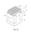
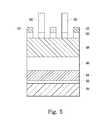
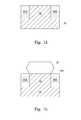
- FIGS. 1A through 1Cillustrate a perspective view and cross-sectional views of FinFET 10 , which is a multi-fin FinFET comprises a plurality of fins 30 (not shown in FIG. 1A , please refer to FIG. 1B ).
- FinFET 10is formed on semiconductor substrate 20 , wherein fins 30 may be formed from semiconductor substrate 20 .
- Gate electrode 26is formed on the plurality of fins.
- FinFET 10further includes source/drain region 32 , and gate spacers 28 ( FIG. 1A ).
- Insulation regions 24 Awhich may be STI regions, are shown in FIG. 1A , and are referred to as inter-device STI regions hereinafter.
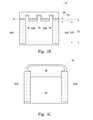
- FIG. 1Billustrates a cross-sectional view of FinFET 10 as shown in FIG. 1A , wherein the cross-sectional view is taken along a plane crossing line 1 B- 1 B in FIG. 1A , which plane crosses gate electrode 26 and gate dielectric 27 .
- gate electrode 26 and gate dielectric 27are formed on the top surfaces and sidewalls of fins 30 .
- Intra-device STI regions 24 Bare formed between fins 30
- inter-device STI regions 24 Aare formed to space FinFET 10 apart from other FinFETs (not shown). Height T 1 of inter-device STI regions 24 A is greater than height T 2 of intra-device STI regions 24 B.
- a ratio of height T 1 to height T 2may be greater than 1.2, greater than about 1.5, greater than about 2.0, or even greater than about 4.0.
- the top surfaces of inter-device STI regions 24 Amay be substantially leveled with the top surfaces of intra-device STI regions 24 B, with the difference less than 10 percent of height T 2 , for example.
- bottom surfaces of intra-device STI regions 24 B and bottom surfaces of inter-device STI regions 24 Amay have a vertical distance AD greater than about 10 nm, or even greater than about 550 nm.
- inter-device STI regions 24 A and intra-device STI regions 24 Bmay be formed of silicon oxide or other known dielectric materials. It is observed that fins 30 and an underlying portion of semiconductor substrate 20 in combination have a crown shape, and hence the respective active region (alternatively referred to OD) is referred to as a crown OD.
- FIG. 1Cillustrates a cross-sectional view of FinFET 10 , wherein the cross-sectional view is taken along a plane crossing line 1 C- 1 C in FIG. 1A , which plane crosses source/drain region 32 .
- fins 30are removed from the plane as shown in FIG. 1C , and source/drain stressors, such as SiGe, SiC, III-V compound semiconductors, or the like, may be re-grown to form source/drain region 32 .
- intra-device STI regions 24 Bare also removed from the plane as shown in FIG. 1C , although they are formed in the plane before being removed. Accordingly, bulk source/drain region 32 is formed. With the formation of bulk source/drain region 32 , the stress in the channel region of FinFET 10 is improved, resulting in an increase in the drive current.
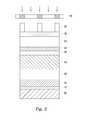
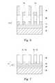
- FIGS. 2 through 15illustrate cross-sectional views of intermediate stages in the manufacturing of FinFET 10 .
- FIGS. 2 through 6illustrate the formation of double-patterning patterns, wherein FIGS. 2 and 3 illustrate the formation (and the removal) of photo resist 58 using a first lithography mask of a double-patterning mask set, and FIGS. 4 through 6 illustrate the formation (and the removal) of second photo resist 66 using a second lithography mask of the same double-patterning mask set.
- substrate 20is provided.
- Substrate 20may be formed of a commonly used semiconductor material such as silicon, silicon germanium, or the like.
- pad oxide layer 42is formed on substrate 20 .
- Hard mask layer 44(which may be a silicon nitride layer) is formed over pad oxide layer 42 .
- Plasma enhanced (PE) oxide layer 46which may be a silicon oxide layer formed using plasma enhanced chemical vapor deposition (PECVD), is formed over hard mask layer 44 .
- Ashing removable dielectric (ARD) 48which may be formed of hydrocarbon, for example, is formed over PE oxide layer 46 .
- PE oxide layer 50 , silicon oxynitride layer 52 , bottom layer 54 , and middle layer 56may be formed sequentially. Bottom layer 54 and middle layer 56 may be formed of carbon-doped polyimide, for example.
- Photo resist 58is applied and patterned using lithography mask 60 , which is a first lithography mask of a double-patterning mask set.
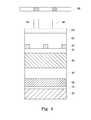
- middle layer 56 , bottom layer 54 , and silicon oxynitride layer 52are patterned, followed by the removal of photo resist 58 and layers 56 and 54 .
- bottom layer 62 and middle layer 64are formed, wherein bottom layer 62 and middle layer 64 may be formed of essentially the same materials as that of layers 54 and 56 , respectively.
- Photo resist 66is applied and patterned using lithography mask 68 .
- Lithography masks 60 ( FIG. 2) and 68are masks of the same double-patterning mask set.
- photo resist 66is removed, followed by the removal of middle layer 64 , as shown in FIG. 5 .
- the pitch of the resulting fins 30 as shown in FIG. 1Bmay be reduced.
- the patterns defined in the preceding process stepsare transferred into ARD 48 , PE oxide layer 46 , and hard mask layer 44 .
- the overlying layers 50 , 52 , and 62are then removed.
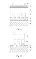
- the remaining portions of ARD 48are then removed, and the resulting structure is shown in FIG. 7 .
- Openings 70extend into hard mask layer 44 for depth D 1 .
- hard mask layer 44includes first portions having first height H 1 , and second portions having second height H 2 .
- Depth D 1may be adjusted to adjust the ratio of height T 2 to height T 1 (please refer to FIG. 1B ), as will be discussed in detail.
- bottom layer 72 and middle layer 74are formed, followed by the formation and the patterning of photo resist 76 .
- Middle layer 74 and bottom layer 72are then patterned, followed by the removal of middle layer 74 , and the resulting structure is shown in FIG. 9 .
- Bottom layer 72is then used as a mask to etch exposed portions of hard mask layer 44 and pad oxide layer 42 , while the portion of hard mask layer 44 covered by bottom layer 72 is protected.
- FIG. 10illustrates the structure after the removal of bottom layer 72 .
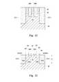
- FIG. 11illustrates the etching of substrate 20 , for example, using an anisotropic etching method such as a dry etch.
- Inter-device STI openings 80 A and intra-device STI openings 80 Bare hence formed.
- the first portions of substrate 20 not covered by hard mask layer 44are etched more to depth D 2 to form inter-device STI openings 80 A.
- the second portions of substrate 20 covered by hard mask layer 44 and PE oxide layer 46are not etched.
- the third portions of substrate 20 that are not covered by PE oxide layer 46 , but are covered by hard mask layer 44are also etched to form intra-device STI openings 80 B, which have depth D 3 smaller than depth D 2 .
- the crown OD 81is thus formed.
- depth D 2is greater than about 20 nm, and may be between about 20 nm and about 700 nm
- depth D 3is smaller than about 10 nm, and may be between about 10 nm and about 150 nm.
- FIG. 12illustrates the filling of a dielectric material, for example, an oxide, to form inter-device STI regions 24 A and intra-device STI regions 24 B.
- a dielectric materialfor example, an oxide
- hard mask layer 44 and possibly pad oxide layer 42are removed, and STI regions 24 A and 24 B are etched back, so that remaining portions of substrate 20 that are above the top surfaces of STI regions 24 A and 24 B form fins 30 .
- the resulting structureis shown in FIG. 13 . It is observed that two of fins 30 , which are marked as fins 30 A, have sidewalls 30 ′ vertically aligned to sidewalls 24 A′ of inter-device STI regions 24 A, and sidewalls 30 ′′ vertically aligned to sidewalls 24 B′ of intra-device STI regions 24 B.
- FIG. 13corresponds to the structure shown in FIG. 1B , except gate dielectric 27 and gate electrode 26 have not been formed yet. In subsequent process steps, gate dielectric 27 and gate electrode 26 are formed, and the structure as shown in FIG. 1B is formed.
- FIGS. 14 and 15illustrate the formation of source/drain regions 32 .
- the cross-sectional views shown in FIGS. 14 and 15are obtained in the plane crossing line 1 C- 1 C in FIG. 1A .
- fins 30 and intra-device STI regions 24 Bare etched. It is noted that in this etching step, only portions of fins 30 that are not protected by gate electrode 26 and gate dielectric 27 ( FIG. 1B ) are etched, while portions of fins 30 directly under gate electrode 26 and gate dielectric 27 are not etched.
- source/drain stressor region 32is epitaxially grown from surface 10 a of semiconductor substrate 20 .
- source/drain region 32is formed of SiGe (for a p-type FinFET) or SiC (for an n-type FinFET). It is observed that since portions of intra-device STI regions 24 B are removed in the step shown in FIG. 14 , intra-device STI regions 24 B do not extend into, or extend directly under, source/drain stressor region 32 .
- FIGS. 16 through 19illustrate cross-sectional views of intermediate stages in the manufacturing of fins and STI regions in accordance with another embodiment.
- the materials and formation methods of the components in this embodimentare essentially the same as the like components, which are denoted by like reference numerals in the embodiment shown in FIGS. 2 through 15 .
- the initial steps of this embodimentare essentially the same as shown in FIGS. 2 through 7 , except pad oxide layer 42 may be partially patterned to a depth between the top surface and the bottom surface of pad oxide layer 42 .
- bottom layer 72 , middle layer 74 , and photo resist 76are formed, followed by the patterning of middle layer 74 and photo resist 76 .
- FIG. 16bottom layer 72 , middle layer 74 , and photo resist 76 are formed, followed by the patterning of middle layer 74 and photo resist 76 .
- opening 70extends to the top surface of substrate 20 .
- bottom layer 72 , middle layer 74 , and photo resist 76are removed.
- inter-device STI opening 80 A and intra-device STI openings 80 Bwhich have different depths D 2 and D 3 .
- inter-device STI opening 80 Ais filled to form inter-device STI region 24 A
- intra-device openings 80 Bare filled to form intra-device STI regions 24 B.
- the subsequent process stepsmay be essentially the same as shown in FIGS. 12 through 15 , and hence are not repeated herein.
- intra-device STI openings 80 Bhave small depths.
- the gap-filling of intra-device openings 80 B(refer to FIGS. 11 and 19 ) is thus easier, and voids are unlikely to occur in the resulting intra-devices STI regions 24 B ( FIG. 1B ).
- intra-device STI regions 24 Bmay be easily removed before source/drain stressors are epitaxially grown. Accordingly, a bulk source/drain stressor having the size expanding across multiple fins may be formed, which means a greater stress may be applied to the channel region of the respective FinFET, and the device current of the FinFET may be improved.
Landscapes
- Insulated Gate Type Field-Effect Transistor (AREA)
Abstract
Description
- This application relates to the following U.S. patent application Ser. No. 12/843,728, filed Jul. 26, 2010, and entitled “Cross OD FinFET Patterning,” which application is hereby incorporated herein by reference.
- This application relates generally to integrated circuits, and more particularly to fin field-effect transistors (FinFETs) and methods of forming the same.
- With the increasing down-scaling of integrated circuits and increasingly demanding requirements to the speed of integrated circuits, transistors need to have higher drive currents with smaller dimensions. Fin field-effect transistors (FinFET) were thus developed. FinFET transistors have increased channel widths, which channels include the channels formed on the sidewalls of the fins and the channels on the top surfaces of the fins. Since the drive currents of transistors are proportional to the channel widths, the drive currents of FinFETs are increased.
- To maximize the channel width of a FinFET, the FinFET may include multiple fins, with the ends of the fins connected to a same source and a same drain. In conventional processes, the formation of a multi-fin FinFET include forming a plurality of fins parallel to each other, forming a gate stack on the plurality of fins, and interconnecting the ends of the plurality of fins to form a source region and a drain region. An epitaxy process may be performed to grow a semiconductor material so that the ends of the plurality of fins merge with each other to form block source and drain regions. Source and drain contact plugs are then formed to connect to the block source and drain regions. This method, however, suffers from gap filling problems. For example, the distance between the fins that belong to the same FinFET is typically very small. Accordingly, it is difficult to perform the gap-filling to fill a dielectric material into the space between the fins.
- In accordance with one aspect, a device includes a plurality of intra-device insulation regions having a first height; and a plurality of semiconductor fins horizontally spaced apart from each other by the plurality of intra-device insulation regions. A portion of the plurality of semiconductor fins is disposed above the plurality of intra-device insulation regions. The device further includes a first inter-device insulation region and a second inter-device insulation region with the plurality of semiconductor fins disposed therebetween. The first and the second inter-device insulation regions have a second height greater than the first height.
- Other embodiments are also disclosed.
- For a more complete understanding of the embodiments, and the advantages thereof, reference is now made to the following descriptions taken in conjunction with the accompanying drawings, in which:
FIG. 1A through 1C illustrate a perspective view and cross-sectional views of a fin field-effect transistor (FinFET) in accordance with an embodiment;FIGS. 2 through 15 are cross-sectional views of intermediate stages in the manufacturing of semiconductor fins, intra-device shallow trench isolation (STI) regions, and inter-device STI regions; andFIGS. 16 through 19 are cross-sectional views of intermediate stages in the manufacturing of semiconductor fins, intra-device STI regions, and inter-device STI regions in accordance with various other embodiments.- The making and using of the embodiments of the disclosure are discussed in detail below. It should be appreciated, however, that the embodiments provide many applicable inventive concepts that can be embodied in a wide variety of specific contexts. The specific embodiments discussed are merely illustrative, and do not limit the scope of the disclosure.
- A novel method for forming semiconductor fins, which may be used for forming fin field-effect transistors (FinFETs) and shallow trench isolation (STI) regions, is provided in accordance with various embodiments. The intermediate stages of manufacturing various embodiments are illustrated. Throughout the various views and illustrative embodiments, like reference numbers are used to designate like elements.
FIGS. 1A through 1C illustrate a perspective view and cross-sectional views of FinFET10, which is a multi-fin FinFET comprises a plurality of fins30 (not shown inFIG. 1A , please refer toFIG. 1B ). FinFET10 is formed onsemiconductor substrate 20, wherein fins30 may be formed fromsemiconductor substrate 20.Gate electrode 26 is formed on the plurality of fins. FinFET10 further includes source/drain region 32, and gate spacers28 (FIG. 1A ).Insulation regions 24A, which may be STI regions, are shown inFIG. 1A , and are referred to as inter-device STI regions hereinafter.FIG. 1B illustrates a cross-sectional view ofFinFET 10 as shown inFIG. 1A , wherein the cross-sectional view is taken along aplane crossing line 1B-1B inFIG. 1A , which plane crossesgate electrode 26 and gate dielectric27. As shown inFIG. 1B ,gate electrode 26 and gate dielectric27 are formed on the top surfaces and sidewalls offins 30. Intra-deviceSTI regions 24B are formed betweenfins 30, whileinter-device STI regions 24A are formed tospace FinFET 10 apart from other FinFETs (not shown). Height T1 ofinter-device STI regions 24A is greater than height T2 ofintra-device STI regions 24B. A ratio of height T1 to height T2 may be greater than 1.2, greater than about 1.5, greater than about 2.0, or even greater than about 4.0. Further, the top surfaces ofinter-device STI regions 24A may be substantially leveled with the top surfaces ofintra-device STI regions 24B, with the difference less than 10 percent of height T2, for example. On the other hand, bottom surfaces ofintra-device STI regions 24B and bottom surfaces ofinter-device STI regions 24A may have a vertical distance AD greater than about 10 nm, or even greater than about 550 nm. In an embodiment,inter-device STI regions 24A andintra-device STI regions 24B may be formed of silicon oxide or other known dielectric materials. It is observed thatfins 30 and an underlying portion ofsemiconductor substrate 20 in combination have a crown shape, and hence the respective active region (alternatively referred to OD) is referred to as a crown OD.FIG. 1C illustrates a cross-sectional view ofFinFET 10, wherein the cross-sectional view is taken along aplane crossing line 1C-1C inFIG. 1A , which plane crosses source/drain region 32. In an embodiment,fins 30 are removed from the plane as shown inFIG. 1C , and source/drain stressors, such as SiGe, SiC, III-V compound semiconductors, or the like, may be re-grown to form source/drain region 32. Similarly,intra-device STI regions 24B are also removed from the plane as shown inFIG. 1C , although they are formed in the plane before being removed. Accordingly, bulk source/drain region 32 is formed. With the formation of bulk source/drain region 32, the stress in the channel region ofFinFET 10 is improved, resulting in an increase in the drive current.FIGS. 2 through 15 illustrate cross-sectional views of intermediate stages in the manufacturing ofFinFET 10.FIGS. 2 through 6 illustrate the formation of double-patterning patterns, whereinFIGS. 2 and 3 illustrate the formation (and the removal) of photo resist58 using a first lithography mask of a double-patterning mask set, andFIGS. 4 through 6 illustrate the formation (and the removal) of second photo resist66 using a second lithography mask of the same double-patterning mask set. Referring toFIG. 2 ,substrate 20 is provided.Substrate 20 may be formed of a commonly used semiconductor material such as silicon, silicon germanium, or the like. In an embodiment,pad oxide layer 42 is formed onsubstrate 20. Hard mask layer44 (which may be a silicon nitride layer) is formed overpad oxide layer 42. Plasma enhanced (PE)oxide layer 46, which may be a silicon oxide layer formed using plasma enhanced chemical vapor deposition (PECVD), is formed overhard mask layer 44. Ashing removable dielectric (ARD)48, which may be formed of hydrocarbon, for example, is formed overPE oxide layer 46. In addition,PE oxide layer 50,silicon oxynitride layer 52,bottom layer 54, andmiddle layer 56 may be formed sequentially.Bottom layer 54 andmiddle layer 56 may be formed of carbon-doped polyimide, for example. Photo resist58 is applied and patterned usinglithography mask 60, which is a first lithography mask of a double-patterning mask set.- Next, as shown in
FIG. 3 ,middle layer 56,bottom layer 54, andsilicon oxynitride layer 52 are patterned, followed by the removal of photo resist58 and layers56 and54. InFIG. 4 ,bottom layer 62 andmiddle layer 64 are formed, whereinbottom layer 62 andmiddle layer 64 may be formed of essentially the same materials as that oflayers lithography mask 68. Lithography masks60 (FIG. 2) and 68 are masks of the same double-patterning mask set. After the patterning ofbottom layer 62 andmiddle layer 64, photo resist66 is removed, followed by the removal ofmiddle layer 64, as shown inFIG. 5 . By using the double-patterning technology, the pitch of the resultingfins 30 as shown inFIG. 1B may be reduced. - In
FIG. 6 , the patterns defined in the preceding process steps are transferred intoARD 48,PE oxide layer 46, andhard mask layer 44. The overlying layers50,52, and62 are then removed. The remaining portions ofARD 48 are then removed, and the resulting structure is shown inFIG. 7 .Openings 70 extend intohard mask layer 44 for depth D1. Accordingly,hard mask layer 44 includes first portions having first height H1, and second portions having second height H2. Depth D1 may be adjusted to adjust the ratio of height T2 to height T1 (please refer toFIG. 1B ), as will be discussed in detail. - Next, as shown in
FIG. 8 ,bottom layer 72 andmiddle layer 74 are formed, followed by the formation and the patterning of photo resist76.Middle layer 74 andbottom layer 72 are then patterned, followed by the removal ofmiddle layer 74, and the resulting structure is shown inFIG. 9 .Bottom layer 72 is then used as a mask to etch exposed portions ofhard mask layer 44 andpad oxide layer 42, while the portion ofhard mask layer 44 covered bybottom layer 72 is protected.FIG. 10 illustrates the structure after the removal ofbottom layer 72. FIG. 11 illustrates the etching ofsubstrate 20, for example, using an anisotropic etching method such as a dry etch.Inter-device STI openings 80A andintra-device STI openings 80B are hence formed. In the etching process, the first portions ofsubstrate 20 not covered byhard mask layer 44 are etched more to depth D2 to forminter-device STI openings 80A. The second portions ofsubstrate 20 covered byhard mask layer 44 andPE oxide layer 46 are not etched. The third portions ofsubstrate 20 that are not covered byPE oxide layer 46, but are covered byhard mask layer 44 are also etched to formintra-device STI openings 80B, which have depth D3 smaller than depth D2. Thecrown OD 81 is thus formed. In an exemplary embodiment, depth D2 is greater than about 20 nm, and may be between about 20 nm and about 700 nm, while depth D3 is smaller than about 10 nm, and may be between about 10 nm and about 150 nm.FIG. 12 illustrates the filling of a dielectric material, for example, an oxide, to forminter-device STI regions 24A andintra-device STI regions 24B. Next,hard mask layer 44 and possibly padoxide layer 42 are removed, andSTI regions substrate 20 that are above the top surfaces ofSTI regions 24 B form fins 30. The resulting structure is shown inFIG. 13 . It is observed that two offins 30, which are marked asfins 30A, have sidewalls30′ vertically aligned to sidewalls24A′ ofinter-device STI regions 24A, and sidewalls30″ vertically aligned to sidewalls24B′ ofintra-device STI regions 24B. The structure shown inFIG. 13 corresponds to the structure shown inFIG. 1B , exceptgate dielectric 27 andgate electrode 26 have not been formed yet. In subsequent process steps,gate dielectric 27 andgate electrode 26 are formed, and the structure as shown inFIG. 1B is formed.FIGS. 14 and 15 illustrate the formation of source/drain regions 32. The cross-sectional views shown inFIGS. 14 and 15 are obtained in theplane crossing line 1C-1C inFIG. 1A . Referring toFIG. 14 ,fins 30 andintra-device STI regions 24B are etched. It is noted that in this etching step, only portions offins 30 that are not protected bygate electrode 26 and gate dielectric27 (FIG. 1B ) are etched, while portions offins 30 directly undergate electrode 26 andgate dielectric 27 are not etched. Next, source/drain stressor region 32 is epitaxially grown from surface10aofsemiconductor substrate 20. In an exemplary embodiment, source/drain region 32 is formed of SiGe (for a p-type FinFET) or SiC (for an n-type FinFET). It is observed that since portions ofintra-device STI regions 24B are removed in the step shown inFIG. 14 ,intra-device STI regions 24B do not extend into, or extend directly under, source/drain stressor region 32.FIGS. 16 through 19 illustrate cross-sectional views of intermediate stages in the manufacturing of fins and STI regions in accordance with another embodiment. Unless specified otherwise, the materials and formation methods of the components in this embodiment are essentially the same as the like components, which are denoted by like reference numerals in the embodiment shown inFIGS. 2 through 15 . The initial steps of this embodiment are essentially the same as shown inFIGS. 2 through 7 , exceptpad oxide layer 42 may be partially patterned to a depth between the top surface and the bottom surface ofpad oxide layer 42. Next, as shown inFIG. 16 ,bottom layer 72,middle layer 74, and photo resist76 are formed, followed by the patterning ofmiddle layer 74 and photo resist76. InFIG. 17 , portions oflayers substrate 20. InFIG. 18 ,bottom layer 72,middle layer 74, and photo resist76 are removed.- In
FIG. 19 , the remaining portions ofpad oxide layer 42,hard mask layer 44, andPE oxide layer 46 are used as masks to forminter-device STI opening 80A andintra-device STI openings 80B, which have different depths D2 and D3. In subsequent steps (not shown),inter-device STI opening 80A is filled to forminter-device STI region 24A, andintra-device openings 80B are filled to formintra-device STI regions 24B. The subsequent process steps may be essentially the same as shown inFIGS. 12 through 15 , and hence are not repeated herein. - In the embodiments,
intra-device STI openings 80B have small depths. The gap-filling ofintra-device openings 80B (refer toFIGS. 11 and 19 ) is thus easier, and voids are unlikely to occur in the resultingintra-devices STI regions 24B (FIG. 1B ). Further, with the small depths T2 ofintra-device STI regions 24B (FIG. 13 ),intra-device STI regions 24B may be easily removed before source/drain stressors are epitaxially grown. Accordingly, a bulk source/drain stressor having the size expanding across multiple fins may be formed, which means a greater stress may be applied to the channel region of the respective FinFET, and the device current of the FinFET may be improved. - Although the embodiments and their advantages have been described in detail, it should be understood that various changes, substitutions and alterations can be made herein without departing from the spirit and scope of the embodiments as defined by the appended claims. Moreover, the scope of the present application is not intended to be limited to the particular embodiments of the process, machine, manufacture, and composition of matter, means, methods and steps described in the specification. As one of ordinary skill in the art will readily appreciate from the disclosure, processes, machines, manufacture, compositions of matter, means, methods, or steps, presently existing or later to be developed, that perform substantially the same function or achieve substantially the same result as the corresponding embodiments described herein may be utilized according to the disclosure. Accordingly, the appended claims are intended to include within their scope such processes, machines, manufacture, compositions of matter, means, methods, or steps. In addition, each claim constitutes a separate embodiment, and the combination of various claims and embodiments are within the scope of the disclosure.
Claims (20)
1. A device comprising:
a plurality of intra-device insulation regions having a first height;
a plurality of semiconductor fins horizontally spaced apart from each other by the plurality of intra-device insulation regions, wherein a portion of the plurality of semiconductor fins is disposed above the plurality of intra-device insulation regions; and
a first inter-device insulation region and a second inter-device insulation region with the plurality of semiconductor fins disposed therebetween, wherein the first and the second inter-device insulation regions have a second height greater than the first height.
2. The device ofclaim 1 , wherein a ratio of the second height to the first height is greater than about 1.2.
3. The device ofclaim 2 , wherein the ratio is greater than about 2.0.
4. The device ofclaim 1 , wherein one of the plurality of semiconductor fins comprises a first sidewall vertically aligned to a sidewall of one of the plurality of intra-device insulation regions, and a second sidewall vertically aligned to a sidewall of the first inter-device insulation region.
5. The device ofclaim 1 further comprising a semiconductor substrate comprising a portion directly under and contacting the plurality of semiconductor fins and the plurality of intra-device insulation regions, wherein the portion of the semiconductor substrate is formed of a same material as the plurality of semiconductor fins.
6. The device ofclaim 5 , wherein the portion of the semiconductor substrate is level with, and horizontally between, the first and the second inter-device insulation regions.
7. The device ofclaim 1 , wherein top surfaces of the plurality of intra-device insulation regions are substantially level with top surfaces of the first and the second inter-device insulation regions, and wherein bottom surfaces of the plurality of intra-device insulation regions are higher than bottom surfaces of the first and the second inter-device insulation regions.
8. The device ofclaim 1 further comprising:
a gate dielectric on top surfaces and sidewalls of the plurality of semiconductor fins; and
a gate electrode directly over the plurality of semiconductor fins and contacting the gate dielectric.
9. The device ofclaim 8 further comprising a semiconductor stressor adjacent the semiconductor fins and formed of a different material from the plurality of semiconductor fins, wherein the plurality of intra-device insulation regions comprises portions directly underlying the gate electrode, and wherein the plurality of intra-device insulation regions does not extend into, or extend directly under, the semiconductor stressor.
10. A device comprising:
a plurality of intra-device insulation regions having a first height;
a plurality of semiconductor fins disposed above top surfaces of, and horizontally spaced apart from each other by, the plurality of intra-device insulation regions; and
a first inter-device insulation region and a second inter-device insulation region with the plurality of semiconductor fins disposed therebetween, wherein first bottom surfaces of the infra-device insulation regions are higher than second bottom surfaces of the first and the second inter-device insulation regions.
11. The device ofclaim 10 , wherein a vertical distance between the first bottom surfaces and the second bottom surfaces is greater than about 10 nm.
12. The device ofclaim 10 , wherein the plurality of semiconductor fins comprises a fin having a first sidewall vertically aligned to a sidewall of one of the plurality of intra-device insulation regions, and a second sidewall vertically aligned to a sidewall of the first inter-device insulation region.
13. The device ofclaim 10 , wherein the first and the second inter-device insulation regions have a second height greater than the first height, and wherein the top surfaces of the plurality of intra-device insulation regions are substantially level with top surfaces of the first and the second inter-device insulation regions.
14. The device ofclaim 10 further comprising:
a gate dielectric on top surfaces and sidewalls of the plurality of semiconductor fins; and
a gate electrode directly over the plurality of semiconductor fins and contacting the gate dielectric; and
a semiconductor stressor adjacent the plurality of semiconductor fins and formed of a different material from the plurality of semiconductor fins, wherein the plurality of intra-device insulation regions comprises portions directly underlying the gate electrode, and wherein the plurality of intra-device insulation regions does not extend into, or extend directly under, the semiconductor stressor.
15. A device comprising:
a plurality of intra-device shallow trench isolation (STI) regions having a first height; and
a fin field-effect transistor (FinFET) comprising:
a crown active region comprising:
a plurality of semiconductor fins disposed above top surfaces of, and horizontally spaced apart from each other by, the plurality of intra-device STI regions; and
a continuous semiconductor region directly underlying, and contacting, the a plurality of semiconductor fins and the plurality of intra-device STI regions, wherein the plurality of semiconductor fins and the continuous semiconductor region are formed of a same semiconductor material;
a gate dielectric on top surfaces and sidewalls of the plurality of semiconductor fins;
a gate electrode over the gate dielectric; and
a source/drain region on a side of the gate electrode, wherein the plurality of intra-device STI regions comprises portions directly underlying the gate electrode, and wherein the plurality of intra-device STI regions does not extend into, or extend directly under, the source/drain region.
16. The device ofclaim 15 further comprising a first inter-device STI region and a second inter-device STI region, wherein the plurality of intra-device STI regions, the plurality of semiconductor fins, and the continuous semiconductor region are horizontally between, and substantially level with, the first and the second inter-device STI regions.
17. The device ofclaim 16 , wherein the top surfaces of the plurality of intra-device STI regions are substantially level with top surfaces of the first and the second inter-device STI regions, and wherein bottom surfaces of the plurality of intra-device STI regions are higher than bottom surfaces of the first and the second inter-device STI regions.
18. The device ofclaim 16 , wherein a first height of the plurality of intra-device STI regions is smaller than a second height of the first and the second inter-device STI regions.
19. A method of forming a multi-digit FinFET device, the method comprising:
providing a semiconductor substrate;
etching the semiconductor substrate to simultaneously form a plurality of intra-device openings and a first and a second inter-device opening in the semiconductor substrate, wherein a first depth of the plurality of intra-device openings is smaller than a second depth of the first and the second inter-device openings;
filling the plurality of intra-device openings to form a plurality of intra-device insulation regions, and filling the first and the second inter-device openings to form a first and a second inter-device insulation region, respectively, wherein the step of filling the plurality of intra-device openings and the step of filling the first and the second inter-device openings are performed simultaneously, and wherein the plurality of intra-device insulation regions are between the first and the second inter-device insulation regions;
etching back the plurality of intra-device insulation regions and the first and the second inter-device insulation regions, wherein remaining portions of the semiconductor substrate above top surfaces of the plurality of intra-device insulation regions form a plurality of semiconductor fins;
forming a gate dielectric on top surfaces and sidewalls of the plurality of semiconductor fins; and
forming a gate electrode on the gate dielectric, wherein a middle portion of each of the plurality of semiconductor fins is covered by the gate dielectric and the gate electrode.
20. The method ofclaim 19 further comprising forming a mask over the semiconductor substrate, wherein the mask comprises first portions having a first height, and second portions having a second height greater than the first height, wherein after the step of etching the semiconductor substrate, first portions of the semiconductor substrate directly underlying the first portions of the mask are etched to form the first and the second inter-device openings, and second portions of the semiconductor substrate directly underlying the second portions of the mask are etched to form the plurality of intra-device openings.
Priority Applications (3)
| Application Number | Priority Date | Filing Date | Title |
|---|---|---|---|
| US12/874,039US9130058B2 (en) | 2010-07-26 | 2010-09-01 | Forming crown active regions for FinFETs |
| CN2011100532616ACN102386230B (en) | 2010-09-01 | 2011-03-03 | Semiconductor device and method for forming multi-bit fin field effect transistor device |
| US14/846,754US9543210B2 (en) | 2010-07-26 | 2015-09-05 | Forming crown active regions for FinFETs |
Applications Claiming Priority (2)
| Application Number | Priority Date | Filing Date | Title |
|---|---|---|---|
| US12/843,728US8110466B2 (en) | 2009-10-27 | 2010-07-26 | Cross OD FinFET patterning |
| US12/874,039US9130058B2 (en) | 2010-07-26 | 2010-09-01 | Forming crown active regions for FinFETs |
Related Child Applications (1)
| Application Number | Title | Priority Date | Filing Date |
|---|---|---|---|
| US14/846,754DivisionUS9543210B2 (en) | 2010-07-26 | 2015-09-05 | Forming crown active regions for FinFETs |
Publications (2)
| Publication Number | Publication Date |
|---|---|
| US20120049294A1true US20120049294A1 (en) | 2012-03-01 |
| US9130058B2 US9130058B2 (en) | 2015-09-08 |
Family
ID=45695999
Family Applications (2)
| Application Number | Title | Priority Date | Filing Date |
|---|---|---|---|
| US12/874,039Active2032-01-05US9130058B2 (en) | 2010-07-26 | 2010-09-01 | Forming crown active regions for FinFETs |
| US14/846,754Expired - Fee RelatedUS9543210B2 (en) | 2010-07-26 | 2015-09-05 | Forming crown active regions for FinFETs |
Family Applications After (1)
| Application Number | Title | Priority Date | Filing Date |
|---|---|---|---|
| US14/846,754Expired - Fee RelatedUS9543210B2 (en) | 2010-07-26 | 2015-09-05 | Forming crown active regions for FinFETs |
Country Status (2)
| Country | Link |
|---|---|
| US (2) | US9130058B2 (en) |
| CN (1) | CN102386230B (en) |
Cited By (31)
| Publication number | Priority date | Publication date | Assignee | Title |
|---|---|---|---|---|
| US20110127610A1 (en)* | 2009-12-02 | 2011-06-02 | Taiwan Semiconductor Manufacturing Company, Ltd. | Multiple-Gate Semiconductor Device and Method |
| US20130119405A1 (en)* | 2011-11-14 | 2013-05-16 | Taiwan Semiconductor Manufacturing Company, Ltd. | Semiconductor device with enhanced strain |
| US8461008B2 (en)* | 2011-08-15 | 2013-06-11 | GlobalFoundries, Inc. | Methods for fabricating FinFET integrated circuits in bulk semiconductor substrates |
| US20130277720A1 (en)* | 2012-04-23 | 2013-10-24 | Samsung Electronics Co., Ltd. | Fin field effect transistors |
| US20140001562A1 (en)* | 2012-06-29 | 2014-01-02 | Taiwan Semiconductor Manufacturing Company, Ltd. | Integrated Circuit Having FinFETS with Different Fin Profiles |
| US8658536B1 (en)* | 2012-09-05 | 2014-02-25 | Globalfoundries Inc. | Selective fin cut process |
| US8716094B1 (en)* | 2012-11-21 | 2014-05-06 | Global Foundries Inc. | FinFET formation using double patterning memorization |
| US8796156B2 (en) | 2009-10-27 | 2014-08-05 | Taiwan Semiconductor Manufacturing Company, Ltd. | Cross OD FinFET patterning |
| US20140342567A1 (en)* | 2012-09-13 | 2014-11-20 | Nanya Technology Corp. | Method of manufacturing semiconductor structure |
| US8916460B1 (en) | 2013-08-07 | 2014-12-23 | Samsung Electronics Co., Ltd. | Semiconductor device and method for fabricating the same |
| US20150145065A1 (en)* | 2013-11-25 | 2015-05-28 | International Business Machines Corporation | finFET Isolation by Selective Cyclic Etch |
| US9130058B2 (en) | 2010-07-26 | 2015-09-08 | Taiwan Semiconductor Manufacturing Company, Ltd. | Forming crown active regions for FinFETs |
| US20160020637A1 (en)* | 2014-07-15 | 2016-01-21 | Rf Micro Devices, Inc. | Wireless charging circuit |
| US20160079799A1 (en)* | 2014-09-16 | 2016-03-17 | Rf Micro Devices, Inc. | Method for wireless charging power control |
| US9385123B2 (en)* | 2014-05-20 | 2016-07-05 | International Business Machines Corporation | STI region for small fin pitch in FinFET devices |
| US9397099B1 (en) | 2015-01-29 | 2016-07-19 | Taiwan Semiconductor Manufacturing Co., Ltd. | Semiconductor device having a plurality of fins and method for fabricating the same |
| US9502410B1 (en)* | 2015-06-09 | 2016-11-22 | United Microelectronics Corp. | Semiconductor structure and manufacturing method thereof |
| US20170077228A1 (en)* | 2015-09-10 | 2017-03-16 | Taiwan Semiconductor Manufacturing Co., Ltd. | Finfet device and method for fabricating the same |
| US9614040B1 (en) | 2016-02-02 | 2017-04-04 | International Business Machines Corporation | Strained silicon germanium fin with block source/drain epitaxy and improved overlay capacitance |
| US9847332B2 (en)* | 2013-08-01 | 2017-12-19 | Taiwan Semiconductor Manufacturing Company, Ltd. | Semiconductor device and fabricating the same |
| US9882054B2 (en)* | 2015-11-12 | 2018-01-30 | United Microelectronics Corp. | FinFET with merged, epitaxial source/drain regions |
| US20180082883A1 (en)* | 2015-09-15 | 2018-03-22 | Taiwan Semiconductor Manufacturing Company, Ltd. | FETS and Methods of Forming FETS |
| US10002962B2 (en)* | 2016-04-27 | 2018-06-19 | International Business Machines Corporation | Vertical FET structure |
| US20180175144A1 (en)* | 2015-09-15 | 2018-06-21 | Taiwan Semiconductor Manufacturing Company, Ltd. | Semiconductor device and manufacturing method thereof |
| CN108573999A (en)* | 2017-03-10 | 2018-09-25 | 三星电子株式会社 | Integrated circuit device and manufacturing method thereof |
| US10205005B1 (en) | 2017-08-10 | 2019-02-12 | United Microelectronics Corp. | Semiconductor device and method for fabricating the same |
| US10217867B2 (en)* | 2016-09-07 | 2019-02-26 | International Business Machines Corporation | Uniform fin dimensions using fin cut hardmask |
| US10224759B2 (en) | 2014-07-15 | 2019-03-05 | Qorvo Us, Inc. | Radio frequency (RF) power harvesting circuit |
| US10879378B2 (en) | 2017-07-24 | 2020-12-29 | United Microelectronics Corp. | Semiconductor structure |
| US20210119013A1 (en)* | 2019-10-18 | 2021-04-22 | Taiwan Semiconductor Manufacturing Company, Ltd. | Semiconductor Device and Method |
| US12094761B2 (en) | 2015-09-15 | 2024-09-17 | Taiwan Semiconductor Manufacturing Company, Ltd. | FETs and methods of forming FETs |
Families Citing this family (12)
| Publication number | Priority date | Publication date | Assignee | Title |
|---|---|---|---|---|
| CN104425339B (en)* | 2013-08-20 | 2017-09-22 | 中芯国际集成电路制造(上海)有限公司 | Forming method for the fleet plough groove isolation structure of fin formula field effect transistor |
| CN105990239B (en)* | 2015-02-06 | 2020-06-30 | 联华电子股份有限公司 | Semiconductor device and method of making the same |
| US10164097B2 (en)* | 2015-09-11 | 2018-12-25 | Taiwan Semiconductor Manufacturing Co., Ltd. | Semiconductor device and manufacturing method thereof |
| US9412648B1 (en) | 2016-01-11 | 2016-08-09 | Taiwan Semiconductor Manufacturing Company, Ltd. | Via patterning using multiple photo multiple etch |
| US10466731B2 (en) | 2016-01-27 | 2019-11-05 | Taiwan Semiconductor Manufacturing Co., Ltd. | Two-transistor bandgap reference circuit and FinFET device suited for same |
| US10115624B2 (en) | 2016-06-30 | 2018-10-30 | Taiwan Semiconductor Manufacturing Co., Ltd. | Method of semiconductor integrated circuit fabrication |
| US10008418B2 (en) | 2016-09-30 | 2018-06-26 | Taiwan Semiconductor Manufacturing Co., Ltd. | Method of semiconductor integrated circuit fabrication |
| JP6689936B2 (en)* | 2018-10-15 | 2020-04-28 | パナソニック株式会社 | Imaging device manufacturing method |
| US20210265350A1 (en)* | 2020-02-26 | 2021-08-26 | Taiwan Semiconductor Manufacturing Co., Ltd. | Semiconductor device and method |
| CN114242643A (en)* | 2020-09-09 | 2022-03-25 | 中芯国际集成电路制造(上海)有限公司 | Method for forming semiconductor structure |
| CN114823530A (en)* | 2022-04-29 | 2022-07-29 | 锐立平芯微电子(广州)有限责任公司 | Method for reducing source-drain short circuit and static random access memory |
| EP4516297A1 (en) | 2022-04-29 | 2025-03-05 | Zhaoke Pharmaceutical (Guangzhou) Co., Ltd | Treprostinil soft mist inhalant |
Citations (2)
| Publication number | Priority date | Publication date | Assignee | Title |
|---|---|---|---|---|
| US20070122953A1 (en)* | 2005-07-01 | 2007-05-31 | Synopsys, Inc. | Enhanced Segmented Channel MOS Transistor with High-Permittivity Dielectric Isolation Material |
| US20080116515A1 (en)* | 2006-11-17 | 2008-05-22 | Infineon Technologies Agam Campeon | Mugfet with increased thermal mass |
Family Cites Families (67)
| Publication number | Priority date | Publication date | Assignee | Title |
|---|---|---|---|---|
| US6737359B1 (en) | 1999-12-13 | 2004-05-18 | Taiwan Semiconductor Manufacturing Company | Method of forming a shallow trench isolation using a sion anti-reflective coating which eliminates water spot defects |
| JP2002118255A (en) | 2000-07-31 | 2002-04-19 | Toshiba Corp | Semiconductor device and manufacturing method thereof |
| JP2002151688A (en) | 2000-08-28 | 2002-05-24 | Mitsubishi Electric Corp | MOS type semiconductor device and method of manufacturing the same |
| CA2342575A1 (en) | 2001-04-03 | 2002-10-03 | Mosaid Technologies Incorporated | Content addressable memory cell |
| US6541351B1 (en) | 2001-11-20 | 2003-04-01 | International Business Machines Corporation | Method for limiting divot formation in post shallow trench isolation processes |
| US6734107B2 (en) | 2002-06-12 | 2004-05-11 | Macronix International Co., Ltd. | Pitch reduction in semiconductor fabrication |
| US7358121B2 (en) | 2002-08-23 | 2008-04-15 | Intel Corporation | Tri-gate devices and methods of fabrication |
| US6706571B1 (en) | 2002-10-22 | 2004-03-16 | Advanced Micro Devices, Inc. | Method for forming multiple structures in a semiconductor device |
| US6949795B2 (en) | 2003-11-13 | 2005-09-27 | Micron Technology, Inc. | Structure and method of fabricating a transistor having a trench gate |
| KR100513405B1 (en) | 2003-12-16 | 2005-09-09 | 삼성전자주식회사 | Method for forming fin field effect transistor |
| WO2005122276A1 (en) | 2004-06-10 | 2005-12-22 | Nec Corporation | Semiconductor device and manufacturing method thereof |
| KR100594282B1 (en) | 2004-06-28 | 2006-06-30 | 삼성전자주식회사 | Semiconductor device comprising FIFNFETT and method for manufacturing same |
| US7512714B2 (en) | 2004-08-31 | 2009-03-31 | Honeywell International Inc. | System and method for transmitting ACARS messages over a TCP/IP data communication link |
| US7115525B2 (en) | 2004-09-02 | 2006-10-03 | Micron Technology, Inc. | Method for integrated circuit fabrication using pitch multiplication |
| US7244640B2 (en) | 2004-10-19 | 2007-07-17 | Taiwan Semiconductor Manufacturing Company, Ltd. | Method for fabricating a body contact in a Finfet structure and a device including the same |
| US7253118B2 (en) | 2005-03-15 | 2007-08-07 | Micron Technology, Inc. | Pitch reduced patterns relative to photolithography features |
| US7508031B2 (en) | 2005-07-01 | 2009-03-24 | Synopsys, Inc. | Enhanced segmented channel MOS transistor with narrowed base regions |
| US7807523B2 (en) | 2005-07-01 | 2010-10-05 | Synopsys, Inc. | Sequential selective epitaxial growth |
| US7265008B2 (en) | 2005-07-01 | 2007-09-04 | Synopsys, Inc. | Method of IC production using corrugated substrate |
| US7190050B2 (en) | 2005-07-01 | 2007-03-13 | Synopsys, Inc. | Integrated circuit on corrugated substrate |
| US8466490B2 (en) | 2005-07-01 | 2013-06-18 | Synopsys, Inc. | Enhanced segmented channel MOS transistor with multi layer regions |
| US7247887B2 (en) | 2005-07-01 | 2007-07-24 | Synopsys, Inc. | Segmented channel MOS transistor |
| US7291560B2 (en) | 2005-08-01 | 2007-11-06 | Infineon Technologies Ag | Method of production pitch fractionizations in semiconductor technology |
| US8003310B2 (en) | 2006-04-24 | 2011-08-23 | Micron Technology, Inc. | Masking techniques and templates for dense semiconductor fabrication |
| US7745319B2 (en) | 2006-08-22 | 2010-06-29 | Micron Technology, Inc. | System and method for fabricating a fin field effect transistor |
| US7858471B2 (en) | 2006-09-13 | 2010-12-28 | Micron Technology, Inc. | Methods of fabricating an access transistor for an integrated circuit device, methods of fabricating periphery transistors and access transistors, and methods of fabricating an access device comprising access transistors in an access circuitry region and peripheral transistors in a peripheral circuitry region spaced from the access circuitry region |
| KR100838378B1 (en) | 2006-09-29 | 2008-06-13 | 주식회사 하이닉스반도체 | Manufacturing Method of Pin Transistor |
| US7560784B2 (en)* | 2007-02-01 | 2009-07-14 | International Business Machines Corporation | Fin PIN diode |
| US7898037B2 (en) | 2007-04-18 | 2011-03-01 | Taiwan Semiconductor Manufacturing Company, Ltd. | Contact scheme for MOSFETs |
| US7939862B2 (en) | 2007-05-30 | 2011-05-10 | Synopsys, Inc. | Stress-enhanced performance of a FinFet using surface/channel orientations and strained capping layers |
| US7807578B2 (en) | 2007-06-01 | 2010-10-05 | Applied Materials, Inc. | Frequency doubling using spacer mask |
| JP2009032955A (en) | 2007-07-27 | 2009-02-12 | Toshiba Corp | Semiconductor device and method for manufacturing the same |
| US8883597B2 (en) | 2007-07-31 | 2014-11-11 | Taiwan Semiconductor Manufacturing Company, Ltd. | Method of fabrication of a FinFET element |
| JP2009152243A (en) | 2007-12-18 | 2009-07-09 | Toshiba Corp | Manufacturing method of semiconductor device |
| US8283231B2 (en) | 2008-06-11 | 2012-10-09 | Taiwan Semiconductor Manufacturing Company, Ltd. | finFET drive strength modification |
| US7910453B2 (en) | 2008-07-14 | 2011-03-22 | Taiwan Semiconductor Manufacturing Company, Ltd. | Storage nitride encapsulation for non-planar sonos NAND flash charge retention |
| US8153493B2 (en) | 2008-08-28 | 2012-04-10 | Taiwan Semiconductor Manufacturing Company, Ltd. | FinFET process compatible native transistor |
| US7829951B2 (en) | 2008-11-06 | 2010-11-09 | Qualcomm Incorporated | Method of fabricating a fin field effect transistor (FinFET) device |
| US7862962B2 (en) | 2009-01-20 | 2011-01-04 | Taiwan Semiconductor Manufacturing Company, Ltd. | Integrated circuit layout design |
| US7989355B2 (en) | 2009-02-12 | 2011-08-02 | Taiwan Semiconductor Manufacturing Company, Ltd. | Method of pitch halving |
| US8053299B2 (en) | 2009-04-17 | 2011-11-08 | Taiwan Semiconductor Manufacturing Company, Ltd. | Method of fabrication of a FinFET element |
| US8357569B2 (en) | 2009-09-29 | 2013-01-22 | Taiwan Semiconductor Manufacturing Company, Ltd. | Method of fabricating finfet device |
| US8110466B2 (en) | 2009-10-27 | 2012-02-07 | Taiwan Semiconductor Manufacturing Company, Ltd. | Cross OD FinFET patterning |
| US8415718B2 (en) | 2009-10-30 | 2013-04-09 | Taiwan Semiconductor Manufacturing Company, Ltd. | Method of forming epi film in substrate trench |
| US8445340B2 (en) | 2009-11-19 | 2013-05-21 | Taiwan Semiconductor Manufacturing Company, Ltd. | Sacrificial offset protection film for a FinFET device |
| US9117905B2 (en) | 2009-12-22 | 2015-08-25 | Taiwan Semiconductor Manufacturing Company, Ltd. | Method for incorporating impurity element in EPI silicon process |
| US8310013B2 (en) | 2010-02-11 | 2012-11-13 | Taiwan Semiconductor Manufacturing Company, Ltd. | Method of fabricating a FinFET device |
| US8212295B2 (en) | 2010-06-30 | 2012-07-03 | Taiwan Semiconductor Manufacturing Company, Ltd. | ROM cell circuit for FinFET devices |
| US8399931B2 (en) | 2010-06-30 | 2013-03-19 | Taiwan Semiconductor Manufacturing Company, Ltd. | Layout for multiple-fin SRAM cell |
| US8942030B2 (en) | 2010-06-25 | 2015-01-27 | Taiwan Semiconductor Manufacturing Company, Ltd. | Structure and method for SRAM cell circuit |
| US8675397B2 (en) | 2010-06-25 | 2014-03-18 | Taiwan Semiconductor Manufacturing Company, Ltd. | Cell structure for dual-port SRAM |
| US8881084B2 (en) | 2010-05-14 | 2014-11-04 | Taiwan Semiconductor Manufacturing Company, Ltd. | FinFET boundary optimization |
| US8621398B2 (en) | 2010-05-14 | 2013-12-31 | Taiwan Semiconductor Manufacturing Company, Ltd. | Automatic layout conversion for FinFET device |
| US8729627B2 (en) | 2010-05-14 | 2014-05-20 | Taiwan Semiconductor Manufacturing Company, Ltd. | Strained channel integrated circuit devices |
| US8278173B2 (en) | 2010-06-30 | 2012-10-02 | Taiwan Semiconductor Manufacturing Company, Ltd. | Method of fabricating gate structures |
| US20120009690A1 (en) | 2010-07-12 | 2012-01-12 | Taiwan Semiconductor Manufacturing Company, Ltd. | In-situ spectrometry |
| US8796759B2 (en) | 2010-07-15 | 2014-08-05 | Taiwan Semiconductor Manufacturing Company, Ltd. | Fin-like field effect transistor (FinFET) device and method of manufacturing same |
| US8278196B2 (en) | 2010-07-21 | 2012-10-02 | Taiwan Semiconductor Manufacturing Company, Ltd. | High surface dopant concentration semiconductor device and method of fabricating |
| US9130058B2 (en) | 2010-07-26 | 2015-09-08 | Taiwan Semiconductor Manufacturing Company, Ltd. | Forming crown active regions for FinFETs |
| US8373229B2 (en) | 2010-08-30 | 2013-02-12 | Taiwan Semiconductor Manufacturing Company, Ltd. | Gate controlled bipolar junction transistor on fin-like field effect transistor (FinFET) structure |
| US8062963B1 (en) | 2010-10-08 | 2011-11-22 | Taiwan Semiconductor Manufacturing Company, Ltd. | Method of fabricating a semiconductor device having an epitaxy region |
| US8367498B2 (en) | 2010-10-18 | 2013-02-05 | Taiwan Semiconductor Manufacturing Company, Ltd. | Fin-like field effect transistor (FinFET) device and method of manufacturing same |
| US9166022B2 (en) | 2010-10-18 | 2015-10-20 | Taiwan Semiconductor Manufacturing Company, Ltd. | Fin-like field effect transistor (FinFET) device and method of manufacturing same |
| US8338305B2 (en) | 2010-10-19 | 2012-12-25 | Taiwan Semiconductor Manufacturing Company, Ltd. | Multi-fin device by self-aligned castle fin formation |
| US8486769B2 (en) | 2010-11-19 | 2013-07-16 | Taiwan Semiconductor Manufacturing Company, Ltd. | Method for forming metrology structures from fins in integrated circuitry |
| US8633076B2 (en) | 2010-11-23 | 2014-01-21 | Taiwan Semiconductor Manufacturing Company, Ltd. | Method for adjusting fin width in integrated circuitry |
| US8525267B2 (en) | 2010-11-23 | 2013-09-03 | Taiwan Semiconductor Manufacturing Company, Ltd. | Device and method for forming Fins in integrated circuitry |
- 2010
- 2010-09-01USUS12/874,039patent/US9130058B2/enactiveActive
- 2011
- 2011-03-03CNCN2011100532616Apatent/CN102386230B/enactiveActive
- 2015
- 2015-09-05USUS14/846,754patent/US9543210B2/ennot_activeExpired - Fee Related
Patent Citations (2)
| Publication number | Priority date | Publication date | Assignee | Title |
|---|---|---|---|---|
| US20070122953A1 (en)* | 2005-07-01 | 2007-05-31 | Synopsys, Inc. | Enhanced Segmented Channel MOS Transistor with High-Permittivity Dielectric Isolation Material |
| US20080116515A1 (en)* | 2006-11-17 | 2008-05-22 | Infineon Technologies Agam Campeon | Mugfet with increased thermal mass |
Cited By (76)
| Publication number | Priority date | Publication date | Assignee | Title |
|---|---|---|---|---|
| US8796156B2 (en) | 2009-10-27 | 2014-08-05 | Taiwan Semiconductor Manufacturing Company, Ltd. | Cross OD FinFET patterning |
| US8895383B2 (en) | 2009-12-02 | 2014-11-25 | Taiwan Semiconductor Manufacturing Company, Ltd. | Multiple-gate semiconductor device and method |
| US8426923B2 (en)* | 2009-12-02 | 2013-04-23 | Taiwan Semiconductor Manufacturing Company, Ltd. | Multiple-gate semiconductor device and method |
| US20110127610A1 (en)* | 2009-12-02 | 2011-06-02 | Taiwan Semiconductor Manufacturing Company, Ltd. | Multiple-Gate Semiconductor Device and Method |
| US9373704B2 (en) | 2009-12-02 | 2016-06-21 | Taiwan Semiconductor Manufacturing Company, Ltd. | Multiple-gate semiconductor device and method |
| US9543210B2 (en) | 2010-07-26 | 2017-01-10 | Taiwan Semiconductor Manufacturing Company, Ltd. | Forming crown active regions for FinFETs |
| US9130058B2 (en) | 2010-07-26 | 2015-09-08 | Taiwan Semiconductor Manufacturing Company, Ltd. | Forming crown active regions for FinFETs |
| US8461008B2 (en)* | 2011-08-15 | 2013-06-11 | GlobalFoundries, Inc. | Methods for fabricating FinFET integrated circuits in bulk semiconductor substrates |
| US20130119405A1 (en)* | 2011-11-14 | 2013-05-16 | Taiwan Semiconductor Manufacturing Company, Ltd. | Semiconductor device with enhanced strain |
| US9601594B2 (en)* | 2011-11-14 | 2017-03-21 | Taiwan Semiconductor Manufacturing Company, Ltd. | Semiconductor device with enhanced strain |
| USRE48367E1 (en)* | 2012-04-23 | 2020-12-22 | Samsung Electronics Co., Ltd. | Field effect transistor having fin base and at least one fin protruding from fin base |
| US20130277720A1 (en)* | 2012-04-23 | 2013-10-24 | Samsung Electronics Co., Ltd. | Fin field effect transistors |
| US8987836B2 (en)* | 2012-04-23 | 2015-03-24 | Samsung Electronics Co., Ltd. | Field effect transistor having fin base and at lease one fin protruding from fin base |
| USRE49375E1 (en)* | 2012-04-23 | 2023-01-17 | Samsung Electronics Co., Ltd. | Field effect transistor having fin base and at least one fin protruding from fin base |
| US20140001562A1 (en)* | 2012-06-29 | 2014-01-02 | Taiwan Semiconductor Manufacturing Company, Ltd. | Integrated Circuit Having FinFETS with Different Fin Profiles |
| US10340270B2 (en) | 2012-06-29 | 2019-07-02 | Taiwan Semiconductor Manufacturing Company | Integrated circuit having FinFETS with different fin profiles |
| US9583398B2 (en)* | 2012-06-29 | 2017-02-28 | Taiwan Semiconductor Manufacturing Company, Ltd. | Integrated circuit having FinFETS with different fin profiles |
| US8658536B1 (en)* | 2012-09-05 | 2014-02-25 | Globalfoundries Inc. | Selective fin cut process |
| US20140342567A1 (en)* | 2012-09-13 | 2014-11-20 | Nanya Technology Corp. | Method of manufacturing semiconductor structure |
| US9779957B2 (en)* | 2012-09-13 | 2017-10-03 | Nanya Technology Corp. | Method of manufacturing independent depth-controlled shallow trench isolation |
| US8716094B1 (en)* | 2012-11-21 | 2014-05-06 | Global Foundries Inc. | FinFET formation using double patterning memorization |
| US9847332B2 (en)* | 2013-08-01 | 2017-12-19 | Taiwan Semiconductor Manufacturing Company, Ltd. | Semiconductor device and fabricating the same |
| US10833084B2 (en) | 2013-08-02 | 2020-11-10 | Taiwan Semiconductor Manufacturing Company, Ltd. | Semiconductor device and fabricating the same |
| US10692865B2 (en) | 2013-08-02 | 2020-06-23 | Taiwan Semiconductor Manufacturing Company, Ltd. | Semiconductor device and fabricating the same |
| US10283508B2 (en) | 2013-08-02 | 2019-05-07 | Taiwan Semiconductor Manufacturing Company, Ltd. | Semiconductor device and fabricating the same |
| US8916460B1 (en) | 2013-08-07 | 2014-12-23 | Samsung Electronics Co., Ltd. | Semiconductor device and method for fabricating the same |
| US9627542B2 (en) | 2013-08-07 | 2017-04-18 | Samsung Electronics Co., Ltd. | Semiconductor device and method for fabricating the same |
| US9190407B2 (en) | 2013-08-07 | 2015-11-17 | Samsung Electronics Co., Ltd. | Semiconductor device and method for fabricating the same |
| CN105190853A (en)* | 2013-11-25 | 2015-12-23 | 国际商业机器公司 | FinFET isolation by selective cyclic etch |
| US20150145065A1 (en)* | 2013-11-25 | 2015-05-28 | International Business Machines Corporation | finFET Isolation by Selective Cyclic Etch |
| WO2015074472A1 (en)* | 2013-11-25 | 2015-05-28 | International Business Machines Corporation | Finfet isolation by selective cyclic etch |
| US9209178B2 (en)* | 2013-11-25 | 2015-12-08 | International Business Machines Corporation | finFET isolation by selective cyclic etch |
| US9385123B2 (en)* | 2014-05-20 | 2016-07-05 | International Business Machines Corporation | STI region for small fin pitch in FinFET devices |
| US20160020637A1 (en)* | 2014-07-15 | 2016-01-21 | Rf Micro Devices, Inc. | Wireless charging circuit |
| US10224759B2 (en) | 2014-07-15 | 2019-03-05 | Qorvo Us, Inc. | Radio frequency (RF) power harvesting circuit |
| US10566843B2 (en)* | 2014-07-15 | 2020-02-18 | Qorvo Us, Inc. | Wireless charging circuit |
| US20160079799A1 (en)* | 2014-09-16 | 2016-03-17 | Rf Micro Devices, Inc. | Method for wireless charging power control |
| US10559970B2 (en)* | 2014-09-16 | 2020-02-11 | Qorvo Us, Inc. | Method for wireless charging power control |
| US9397099B1 (en) | 2015-01-29 | 2016-07-19 | Taiwan Semiconductor Manufacturing Co., Ltd. | Semiconductor device having a plurality of fins and method for fabricating the same |
| US9659932B2 (en) | 2015-01-29 | 2017-05-23 | Taiwan Semiconductor Manufacturing Co., Ltd. | Semiconductor device having a plurality of fins and method for fabricating the same |
| US9583394B2 (en)* | 2015-06-09 | 2017-02-28 | United Microelectronics Corp. | Manufacturing method of semiconductor structure |
| US9502410B1 (en)* | 2015-06-09 | 2016-11-22 | United Microelectronics Corp. | Semiconductor structure and manufacturing method thereof |
| US10749013B2 (en) | 2015-09-10 | 2020-08-18 | Taiwan Semiconductor Manufacturing Co., Ltd. | Semiconductor device and method for fabricating the same |
| US11948999B2 (en) | 2015-09-10 | 2024-04-02 | Taiwan Semiconductor Manufacturing Co., Ltd. | Semiconductor device |
| US11430878B2 (en) | 2015-09-10 | 2022-08-30 | Taiwan Semiconductor Manufacturing Co., Ltd. | Method for fabricating semiconductor device |
| US20170077228A1 (en)* | 2015-09-10 | 2017-03-16 | Taiwan Semiconductor Manufacturing Co., Ltd. | Finfet device and method for fabricating the same |
| US10103249B2 (en)* | 2015-09-10 | 2018-10-16 | Taiwan Semiconductor Manufacturing Co., Ltd. | FinFET device and method for fabricating the same |
| US11004724B2 (en) | 2015-09-15 | 2021-05-11 | Taiwan Semiconductor Manufacturing Company, Ltd. | FETS and methods of forming FETS |
| US20180175144A1 (en)* | 2015-09-15 | 2018-06-21 | Taiwan Semiconductor Manufacturing Company, Ltd. | Semiconductor device and manufacturing method thereof |
| US11728208B2 (en) | 2015-09-15 | 2023-08-15 | Taiwan Semiconductor Manufacturing Company, Ltd. | FETS and methods of forming FETS |
| US10269618B2 (en)* | 2015-09-15 | 2019-04-23 | Taiwan Semiconductor Manufacturing Company, Ltd. | FETS and methods of forming FETS |
| US12094761B2 (en) | 2015-09-15 | 2024-09-17 | Taiwan Semiconductor Manufacturing Company, Ltd. | FETs and methods of forming FETs |
| US20190252240A1 (en)* | 2015-09-15 | 2019-08-15 | Taiwan Semiconductor Manufacturing Company, Ltd. | FETS and Methods of Forming FETS |
| US10468482B2 (en)* | 2015-09-15 | 2019-11-05 | Taiwan Semiconductor Manufacturing Company, Ltd. | Semiconductor device and manufacturing method thereof |
| US10991795B2 (en) | 2015-09-15 | 2021-04-27 | Taiwan Semiconductor Manufacturing Company, Ltd. | Semiconductor device and manufacturing method thereof |
| US20180082883A1 (en)* | 2015-09-15 | 2018-03-22 | Taiwan Semiconductor Manufacturing Company, Ltd. | FETS and Methods of Forming FETS |
| US9978873B2 (en) | 2015-11-12 | 2018-05-22 | United Microelectronics Corp. | Method for fabricating FinFet |
| US9882054B2 (en)* | 2015-11-12 | 2018-01-30 | United Microelectronics Corp. | FinFET with merged, epitaxial source/drain regions |
| US10600878B2 (en) | 2016-02-02 | 2020-03-24 | International Business Machines Corporation | Strained silicon germanium fin with block source/drain epitaxy and improved overlay capacitance |
| US9614040B1 (en) | 2016-02-02 | 2017-04-04 | International Business Machines Corporation | Strained silicon germanium fin with block source/drain epitaxy and improved overlay capacitance |
| US10283601B2 (en) | 2016-02-02 | 2019-05-07 | International Business Machines Corporation | Strained silicon germanium fin with block source/drain epitaxy and improved overlay capacitance |
| US10347759B2 (en)* | 2016-04-27 | 2019-07-09 | International Business Machines Corporation | Vertical FET structure |
| US10002962B2 (en)* | 2016-04-27 | 2018-06-19 | International Business Machines Corporation | Vertical FET structure |
| US20190140090A1 (en)* | 2016-09-07 | 2019-05-09 | International Business Machines Corporation | Uniform fin dimensions using fin cut hardmask |
| US10217867B2 (en)* | 2016-09-07 | 2019-02-26 | International Business Machines Corporation | Uniform fin dimensions using fin cut hardmask |
| US10854753B2 (en)* | 2016-09-07 | 2020-12-01 | Tessera, Inc. | Uniform fin dimensions using fin cut hardmask |
| CN108573999A (en)* | 2017-03-10 | 2018-09-25 | 三星电子株式会社 | Integrated circuit device and manufacturing method thereof |
| US11316010B2 (en) | 2017-03-10 | 2022-04-26 | Samsung Electronics Co., Ltd. | Integrated circuit device and method of fabricating the same |
| US11769769B2 (en) | 2017-03-10 | 2023-09-26 | Samsung Electronics Co., Ltd. | Integrated circuit device and method of fabricating the same |
| US10879239B2 (en) | 2017-03-10 | 2020-12-29 | Samsung Electronics Co., Ltd. | Integrated circuit device and method of fabricating the same |
| US11264488B2 (en) | 2017-07-24 | 2022-03-01 | United Microelectronics Corp. | Manufacturing method of semiconductor structure |
| US10879378B2 (en) | 2017-07-24 | 2020-12-29 | United Microelectronics Corp. | Semiconductor structure |
| US10312353B2 (en)* | 2017-08-10 | 2019-06-04 | United Microelectronics Corp. | Semiconductor device and method for fabricating the same |
| US10205005B1 (en) | 2017-08-10 | 2019-02-12 | United Microelectronics Corp. | Semiconductor device and method for fabricating the same |
| US11211470B2 (en)* | 2019-10-18 | 2021-12-28 | Taiwan Semiconductor Manufacturing Company, Ltd. | Semiconductor device and method |
| US20210119013A1 (en)* | 2019-10-18 | 2021-04-22 | Taiwan Semiconductor Manufacturing Company, Ltd. | Semiconductor Device and Method |
Also Published As
| Publication number | Publication date |
|---|---|
| US9130058B2 (en) | 2015-09-08 |
| US9543210B2 (en) | 2017-01-10 |
| US20150380315A1 (en) | 2015-12-31 |
| CN102386230A (en) | 2012-03-21 |
| CN102386230B (en) | 2013-10-16 |
Similar Documents
| Publication | Publication Date | Title |
|---|---|---|
| US9543210B2 (en) | Forming crown active regions for FinFETs | |
| US10978355B2 (en) | Multi-gate devices with replaced-channels and methods for forming the same | |
| US10157920B2 (en) | Multi-fin device and method of making same | |
| CN103199010B (en) | Finfet and forming method thereof | |
| US8796156B2 (en) | Cross OD FinFET patterning | |
| TWI514580B (en) | Semiconductor component and method of forming same | |
| KR101441747B1 (en) | STRUCTURE AND METHOD FOR FinFET DEVICE | |
| US11393916B2 (en) | Methods for GAA I/O formation by selective epi regrowth | |
| CN103311296B (en) | There is high mobility and the semiconductor structure of high band gap material and method | |
| US9953975B2 (en) | Methods for forming STI regions in integrated circuits | |
| US8377779B1 (en) | Methods of manufacturing semiconductor devices and transistors | |
| US20070235819A1 (en) | Semiconductor device and method for manufacturing the same | |
| US8062938B2 (en) | Semiconductor device and method of fabricating the same | |
| WO2014059812A1 (en) | Method for manufacturing stacked nano-wire mos transistor | |
| CN103367440A (en) | Fin structure for finfet device | |
| US9209094B2 (en) | Fin field effect transistor with dielectric isolation and anchored stressor elements | |
| US9953976B2 (en) | Effective device formation for advanced technology nodes with aggressive fin-pitch scaling | |
| US20150123211A1 (en) | NARROW DIFFUSION BREAK FOR A FIN FIELD EFFECT (FinFET) TRANSISTOR DEVICE | |
| CN103578996B (en) | Transistor fabrication process | |
| TWI686850B (en) | Semiconductor device and method of fabricating the same | |
| US12046518B2 (en) | Method for manufacturing fin field effect transistor | |
| CN110299286B (en) | Method for manufacturing epitaxial fin-shaped structure | |
| CN117594447A (en) | Fence stack nano-sheet device with high hole mobility channel and preparation method thereof | |
| CN105870014A (en) | Fin forming method |
Legal Events
| Date | Code | Title | Description |
|---|---|---|---|
| AS | Assignment | Owner name:TAIWAN SEMICONDUCTOR MANUFACTURING COMPANY, LTD., Free format text:ASSIGNMENT OF ASSIGNORS INTEREST;ASSIGNORS:CHEN, CHEN-PING;LIN, HUI-MIN;HUANG, MING-JIE;AND OTHERS;SIGNING DATES FROM 20100826 TO 20100827;REEL/FRAME:024929/0513 | |
| STCF | Information on status: patent grant | Free format text:PATENTED CASE | |
| MAFP | Maintenance fee payment | Free format text:PAYMENT OF MAINTENANCE FEE, 4TH YEAR, LARGE ENTITY (ORIGINAL EVENT CODE: M1551); ENTITY STATUS OF PATENT OWNER: LARGE ENTITY Year of fee payment:4 | |
| MAFP | Maintenance fee payment | Free format text:PAYMENT OF MAINTENANCE FEE, 8TH YEAR, LARGE ENTITY (ORIGINAL EVENT CODE: M1552); ENTITY STATUS OF PATENT OWNER: LARGE ENTITY Year of fee payment:8 |