US20120038047A1 - Semiconductor Device and Method of Forming B-Stage Conductive Polymer Over Contact Pads of Semiconductor Die in FO-WLCSP - Google Patents
Semiconductor Device and Method of Forming B-Stage Conductive Polymer Over Contact Pads of Semiconductor Die in FO-WLCSPDownload PDFInfo
- Publication number
- US20120038047A1 US20120038047A1US12/853,898US85389810AUS2012038047A1US 20120038047 A1US20120038047 A1US 20120038047A1US 85389810 AUS85389810 AUS 85389810AUS 2012038047 A1US2012038047 A1US 2012038047A1
- Authority
- US
- United States
- Prior art keywords
- conductive polymer
- semiconductor die
- insulating layer
- semiconductor
- over
- Prior art date
- Legal status (The legal status is an assumption and is not a legal conclusion. Google has not performed a legal analysis and makes no representation as to the accuracy of the status listed.)
- Granted
Links
- 239000004065semiconductorSubstances0.000titleclaimsabstractdescription189
- 229920001940conductive polymerPolymers0.000titleclaimsabstractdescription93
- 238000000034methodMethods0.000titleclaimsdescription47
- 239000008393encapsulating agentSubstances0.000claimsabstractdescription37
- 230000009477glass transitionEffects0.000claimsabstractdescription15
- 239000000463materialSubstances0.000claimsdescription43
- 238000000151depositionMethods0.000claimsdescription20
- 238000004519manufacturing processMethods0.000claimsdescription19
- 238000010438heat treatmentMethods0.000claimsdescription14
- 230000008569processEffects0.000description24
- HCWZEPKLWVAEOV-UHFFFAOYSA-N2,2',5,5'-tetrachlorobiphenylChemical compoundClC1=CC=C(Cl)C(C=2C(=CC=C(Cl)C=2)Cl)=C1HCWZEPKLWVAEOV-UHFFFAOYSA-N0.000description15
- 238000004806packaging method and processMethods0.000description13
- PXHVJJICTQNCMI-UHFFFAOYSA-NNickelChemical compound[Ni]PXHVJJICTQNCMI-UHFFFAOYSA-N0.000description9
- 238000007772electroless platingMethods0.000description9
- 238000009713electroplatingMethods0.000description9
- 239000011135tinSubstances0.000description9
- VYPSYNLAJGMNEJ-UHFFFAOYSA-NSilicium dioxideChemical compoundO=[Si]=OVYPSYNLAJGMNEJ-UHFFFAOYSA-N0.000description8
- 230000006870functionEffects0.000description8
- 239000010931goldSubstances0.000description8
- 229910000679solderInorganic materials0.000description8
- 238000005229chemical vapour depositionMethods0.000description7
- 239000010949copperSubstances0.000description7
- 238000005240physical vapour depositionMethods0.000description7
- 229920000642polymerPolymers0.000description7
- 229910052782aluminiumInorganic materials0.000description6
- 239000003990capacitorSubstances0.000description6
- 239000004020conductorSubstances0.000description6
- 229910052802copperInorganic materials0.000description6
- 229910052737goldInorganic materials0.000description6
- 238000002955isolationMethods0.000description6
- 239000011133leadSubstances0.000description6
- 238000001465metallisationMethods0.000description6
- 229910052759nickelInorganic materials0.000description6
- 229910052709silverInorganic materials0.000description6
- 239000000758substrateSubstances0.000description6
- 229910052718tinInorganic materials0.000description6
- 238000013461designMethods0.000description5
- 238000005530etchingMethods0.000description5
- 238000000465mouldingMethods0.000description5
- 230000003647oxidationEffects0.000description5
- 238000007254oxidation reactionMethods0.000description5
- 229920002120photoresistant polymerPolymers0.000description5
- 238000007639printingMethods0.000description5
- 239000010944silver (metal)Substances0.000description5
- 238000004528spin coatingMethods0.000description5
- 229910052581Si3N4Inorganic materials0.000description4
- 230000005684electric fieldEffects0.000description4
- 239000003822epoxy resinSubstances0.000description4
- TWNQGVIAIRXVLR-UHFFFAOYSA-Noxo(oxoalumanyloxy)alumaneChemical compoundO=[Al]O[Al]=OTWNQGVIAIRXVLR-UHFFFAOYSA-N0.000description4
- BPUBBGLMJRNUCC-UHFFFAOYSA-Noxygen(2-);tantalum(5+)Chemical compound[O-2].[O-2].[O-2].[O-2].[O-2].[Ta+5].[Ta+5]BPUBBGLMJRNUCC-UHFFFAOYSA-N0.000description4
- 229920000647polyepoxidePolymers0.000description4
- 238000012545processingMethods0.000description4
- 238000007650screen-printingMethods0.000description4
- 235000012239silicon dioxideNutrition0.000description4
- 239000000377silicon dioxideSubstances0.000description4
- HQVNEWCFYHHQES-UHFFFAOYSA-Nsilicon nitrideChemical compoundN12[Si]34N5[Si]62N3[Si]51N64HQVNEWCFYHHQES-UHFFFAOYSA-N0.000description4
- 238000005245sinteringMethods0.000description4
- 238000005507sprayingMethods0.000description4
- PBCFLUZVCVVTBY-UHFFFAOYSA-Ntantalum pentoxideInorganic materialsO=[Ta](=O)O[Ta](=O)=OPBCFLUZVCVVTBY-UHFFFAOYSA-N0.000description4
- 239000004593EpoxySubstances0.000description3
- XUIMIQQOPSSXEZ-UHFFFAOYSA-NSiliconChemical compound[Si]XUIMIQQOPSSXEZ-UHFFFAOYSA-N0.000description3
- -1acrylChemical group0.000description3
- 238000004891communicationMethods0.000description3
- 230000008021depositionEffects0.000description3
- 230000007613environmental effectEffects0.000description3
- 230000005496eutecticsEffects0.000description3
- 230000008020evaporationEffects0.000description3
- 238000001704evaporationMethods0.000description3
- 239000000945fillerSubstances0.000description3
- 238000003698laser cuttingMethods0.000description3
- 238000002161passivationMethods0.000description3
- 238000005498polishingMethods0.000description3
- 239000000047productSubstances0.000description3
- 229910052710siliconInorganic materials0.000description3
- 239000010703siliconSubstances0.000description3
- OKTJSMMVPCPJKN-UHFFFAOYSA-NCarbonChemical compound[C]OKTJSMMVPCPJKN-UHFFFAOYSA-N0.000description2
- 230000009471actionEffects0.000description2
- 239000000853adhesiveSubstances0.000description2
- 230000001070adhesive effectEffects0.000description2
- 230000015572biosynthetic processEffects0.000description2
- 229910052797bismuthInorganic materials0.000description2
- 239000000919ceramicSubstances0.000description2
- 239000002131composite materialSubstances0.000description2
- 150000001875compoundsChemical class0.000description2
- 230000006835compressionEffects0.000description2
- 238000007906compressionMethods0.000description2
- 230000005669field effectEffects0.000description2
- 230000004907fluxEffects0.000description2
- 239000011521glassSubstances0.000description2
- 239000012535impuritySubstances0.000description2
- 238000003475laminationMethods0.000description2
- 229910052745leadInorganic materials0.000description2
- 230000008018meltingEffects0.000description2
- 238000002844meltingMethods0.000description2
- 230000015654memoryEffects0.000description2
- 229910052751metalInorganic materials0.000description2
- 239000002184metalSubstances0.000description2
- 238000012986modificationMethods0.000description2
- 230000004048modificationEffects0.000description2
- 239000005022packaging materialSubstances0.000description2
- 239000002245particleSubstances0.000description2
- 238000000059patterningMethods0.000description2
- 238000000206photolithographyMethods0.000description2
- 238000007747platingMethods0.000description2
- 238000004544sputter depositionMethods0.000description2
- 239000000126substanceSubstances0.000description2
- 230000001131transforming effectEffects0.000description2
- FRWYFWZENXDZMU-UHFFFAOYSA-N2-iodoquinolineChemical compoundC1=CC=CC2=NC(I)=CC=C21FRWYFWZENXDZMU-UHFFFAOYSA-N0.000description1
- JBRZTFJDHDCESZ-UHFFFAOYSA-NAsGaChemical compound[As]#[Ga]JBRZTFJDHDCESZ-UHFFFAOYSA-N0.000description1
- RYGMFSIKBFXOCR-UHFFFAOYSA-NCopperChemical compound[Cu]RYGMFSIKBFXOCR-UHFFFAOYSA-N0.000description1
- 229910001218Gallium arsenideInorganic materials0.000description1
- GPXJNWSHGFTCBW-UHFFFAOYSA-NIndium phosphideChemical compound[In]#PGPXJNWSHGFTCBW-UHFFFAOYSA-N0.000description1
- 208000024875Infantile dystonia-parkinsonismDiseases0.000description1
- LIMFPAAAIVQRRD-BCGVJQADSA-NN-[2-[(3S,4R)-3-fluoro-4-methoxypiperidin-1-yl]pyrimidin-4-yl]-8-[(2R,3S)-2-methyl-3-(methylsulfonylmethyl)azetidin-1-yl]-5-propan-2-ylisoquinolin-3-amineChemical compoundF[C@H]1CN(CC[C@H]1OC)C1=NC=CC(=N1)NC=1N=CC2=C(C=CC(=C2C=1)C(C)C)N1[C@@H]([C@H](C1)CS(=O)(=O)C)CLIMFPAAAIVQRRD-BCGVJQADSA-N0.000description1
- BQCADISMDOOEFD-UHFFFAOYSA-NSilverChemical compound[Ag]BQCADISMDOOEFD-UHFFFAOYSA-N0.000description1
- ATJFFYVFTNAWJD-UHFFFAOYSA-NTinChemical compound[Sn]ATJFFYVFTNAWJD-UHFFFAOYSA-N0.000description1
- OFLYIWITHZJFLS-UHFFFAOYSA-N[Si].[Au]Chemical compound[Si].[Au]OFLYIWITHZJFLS-UHFFFAOYSA-N0.000description1
- 239000003082abrasive agentSubstances0.000description1
- 230000006978adaptationEffects0.000description1
- 238000004026adhesive bondingMethods0.000description1
- XAGFODPZIPBFFR-UHFFFAOYSA-NaluminiumChemical compound[Al]XAGFODPZIPBFFR-UHFFFAOYSA-N0.000description1
- LTPBRCUWZOMYOC-UHFFFAOYSA-Nberyllium oxideInorganic materialsO=[Be]LTPBRCUWZOMYOC-UHFFFAOYSA-N0.000description1
- 239000006229carbon blackSubstances0.000description1
- 239000002041carbon nanotubeSubstances0.000description1
- 229910021393carbon nanotubeInorganic materials0.000description1
- 230000015556catabolic processEffects0.000description1
- 230000001413cellular effectEffects0.000description1
- 238000003486chemical etchingMethods0.000description1
- 238000006243chemical reactionMethods0.000description1
- 239000007795chemical reaction productSubstances0.000description1
- 239000011248coating agentSubstances0.000description1
- 238000000576coating methodMethods0.000description1
- 239000000356contaminantSubstances0.000description1
- 238000005336crackingMethods0.000description1
- 238000005520cutting processMethods0.000description1
- 230000003247decreasing effectEffects0.000description1
- 238000006731degradation reactionMethods0.000description1
- 239000003989dielectric materialSubstances0.000description1
- 238000009792diffusion processMethods0.000description1
- 230000009977dual effectEffects0.000description1
- 230000005611electricityEffects0.000description1
- 238000005538encapsulationMethods0.000description1
- 239000010408filmSubstances0.000description1
- 229910052732germaniumInorganic materials0.000description1
- GNPVGFCGXDBREM-UHFFFAOYSA-Ngermanium atomChemical compound[Ge]GNPVGFCGXDBREM-UHFFFAOYSA-N0.000description1
- PCHJSUWPFVWCPO-UHFFFAOYSA-NgoldChemical compound[Au]PCHJSUWPFVWCPO-UHFFFAOYSA-N0.000description1
- 229910002804graphiteInorganic materials0.000description1
- 239000010439graphiteSubstances0.000description1
- 238000000227grindingMethods0.000description1
- 208000001543infantile parkinsonism-dystoniaDiseases0.000description1
- 239000012212insulatorSubstances0.000description1
- 238000005468ion implantationMethods0.000description1
- 230000001788irregularEffects0.000description1
- 239000007788liquidSubstances0.000description1
- 239000011159matrix materialSubstances0.000description1
- 229910044991metal oxideInorganic materials0.000description1
- 150000004706metal oxidesChemical class0.000description1
- 239000002923metal particleSubstances0.000description1
- 150000002739metalsChemical class0.000description1
- 239000012778molding materialSubstances0.000description1
- KCTAWXVAICEBSD-UHFFFAOYSA-Nprop-2-enoyloxy prop-2-eneperoxoateChemical compoundC=CC(=O)OOOC(=O)C=CKCTAWXVAICEBSD-UHFFFAOYSA-N0.000description1
- 230000004044responseEffects0.000description1
- HBMJWWWQQXIZIP-UHFFFAOYSA-Nsilicon carbideChemical compound[Si+]#[C-]HBMJWWWQQXIZIP-UHFFFAOYSA-N0.000description1
- 229910010271silicon carbideInorganic materials0.000description1
- 239000004332silverSubstances0.000description1
- 239000002904solventSubstances0.000description1
- 238000012360testing methodMethods0.000description1
- 238000005382thermal cyclingMethods0.000description1
- 239000010409thin filmSubstances0.000description1
- 238000000427thin-film depositionMethods0.000description1
- 238000012876topographyMethods0.000description1
- 238000001721transfer mouldingMethods0.000description1
- 230000000007visual effectEffects0.000description1
- 239000013585weight reducing agentSubstances0.000description1
Images

Classifications
- H—ELECTRICITY
- H01—ELECTRIC ELEMENTS
- H01L—SEMICONDUCTOR DEVICES NOT COVERED BY CLASS H10
- H01L23/00—Details of semiconductor or other solid state devices
- H01L23/52—Arrangements for conducting electric current within the device in operation from one component to another, i.e. interconnections, e.g. wires, lead frames
- H01L23/538—Arrangements for conducting electric current within the device in operation from one component to another, i.e. interconnections, e.g. wires, lead frames the interconnection structure between a plurality of semiconductor chips being formed on, or in, insulating substrates
- H01L23/5389—Arrangements for conducting electric current within the device in operation from one component to another, i.e. interconnections, e.g. wires, lead frames the interconnection structure between a plurality of semiconductor chips being formed on, or in, insulating substrates the chips being integrally enclosed by the interconnect and support structures
- H—ELECTRICITY
- H01—ELECTRIC ELEMENTS
- H01L—SEMICONDUCTOR DEVICES NOT COVERED BY CLASS H10
- H01L21/00—Processes or apparatus adapted for the manufacture or treatment of semiconductor or solid state devices or of parts thereof
- H01L21/02—Manufacture or treatment of semiconductor devices or of parts thereof
- H01L21/04—Manufacture or treatment of semiconductor devices or of parts thereof the devices having potential barriers, e.g. a PN junction, depletion layer or carrier concentration layer
- H01L21/50—Assembly of semiconductor devices using processes or apparatus not provided for in a single one of the groups H01L21/18 - H01L21/326 or H10D48/04 - H10D48/07 e.g. sealing of a cap to a base of a container
- H01L21/56—Encapsulations, e.g. encapsulation layers, coatings
- H01L21/561—Batch processing
- H—ELECTRICITY
- H01—ELECTRIC ELEMENTS
- H01L—SEMICONDUCTOR DEVICES NOT COVERED BY CLASS H10
- H01L21/00—Processes or apparatus adapted for the manufacture or treatment of semiconductor or solid state devices or of parts thereof
- H01L21/02—Manufacture or treatment of semiconductor devices or of parts thereof
- H01L21/04—Manufacture or treatment of semiconductor devices or of parts thereof the devices having potential barriers, e.g. a PN junction, depletion layer or carrier concentration layer
- H01L21/50—Assembly of semiconductor devices using processes or apparatus not provided for in a single one of the groups H01L21/18 - H01L21/326 or H10D48/04 - H10D48/07 e.g. sealing of a cap to a base of a container
- H01L21/56—Encapsulations, e.g. encapsulation layers, coatings
- H01L21/568—Temporary substrate used as encapsulation process aid
- H—ELECTRICITY
- H01—ELECTRIC ELEMENTS
- H01L—SEMICONDUCTOR DEVICES NOT COVERED BY CLASS H10
- H01L23/00—Details of semiconductor or other solid state devices
- H01L23/28—Encapsulations, e.g. encapsulating layers, coatings, e.g. for protection
- H01L23/31—Encapsulations, e.g. encapsulating layers, coatings, e.g. for protection characterised by the arrangement or shape
- H01L23/3107—Encapsulations, e.g. encapsulating layers, coatings, e.g. for protection characterised by the arrangement or shape the device being completely enclosed
- H01L23/3121—Encapsulations, e.g. encapsulating layers, coatings, e.g. for protection characterised by the arrangement or shape the device being completely enclosed a substrate forming part of the encapsulation
- H01L23/3128—Encapsulations, e.g. encapsulating layers, coatings, e.g. for protection characterised by the arrangement or shape the device being completely enclosed a substrate forming part of the encapsulation the substrate having spherical bumps for external connection
- H—ELECTRICITY
- H01—ELECTRIC ELEMENTS
- H01L—SEMICONDUCTOR DEVICES NOT COVERED BY CLASS H10
- H01L24/00—Arrangements for connecting or disconnecting semiconductor or solid-state bodies; Methods or apparatus related thereto
- H01L24/01—Means for bonding being attached to, or being formed on, the surface to be connected, e.g. chip-to-package, die-attach, "first-level" interconnects; Manufacturing methods related thereto
- H01L24/18—High density interconnect [HDI] connectors; Manufacturing methods related thereto
- H01L24/19—Manufacturing methods of high density interconnect preforms
- H—ELECTRICITY
- H01—ELECTRIC ELEMENTS
- H01L—SEMICONDUCTOR DEVICES NOT COVERED BY CLASS H10
- H01L24/00—Arrangements for connecting or disconnecting semiconductor or solid-state bodies; Methods or apparatus related thereto
- H01L24/01—Means for bonding being attached to, or being formed on, the surface to be connected, e.g. chip-to-package, die-attach, "first-level" interconnects; Manufacturing methods related thereto
- H01L24/18—High density interconnect [HDI] connectors; Manufacturing methods related thereto
- H01L24/20—Structure, shape, material or disposition of high density interconnect preforms
- H—ELECTRICITY
- H01—ELECTRIC ELEMENTS
- H01L—SEMICONDUCTOR DEVICES NOT COVERED BY CLASS H10
- H01L24/00—Arrangements for connecting or disconnecting semiconductor or solid-state bodies; Methods or apparatus related thereto
- H01L24/93—Batch processes
- H01L24/95—Batch processes at chip-level, i.e. with connecting carried out on a plurality of singulated devices, i.e. on diced chips
- H01L24/96—Batch processes at chip-level, i.e. with connecting carried out on a plurality of singulated devices, i.e. on diced chips the devices being encapsulated in a common layer, e.g. neo-wafer or pseudo-wafer, said common layer being separable into individual assemblies after connecting
- H—ELECTRICITY
- H01—ELECTRIC ELEMENTS
- H01L—SEMICONDUCTOR DEVICES NOT COVERED BY CLASS H10
- H01L2224/00—Indexing scheme for arrangements for connecting or disconnecting semiconductor or solid-state bodies and methods related thereto as covered by H01L24/00
- H01L2224/01—Means for bonding being attached to, or being formed on, the surface to be connected, e.g. chip-to-package, die-attach, "first-level" interconnects; Manufacturing methods related thereto
- H01L2224/02—Bonding areas; Manufacturing methods related thereto
- H01L2224/023—Redistribution layers [RDL] for bonding areas
- H01L2224/0231—Manufacturing methods of the redistribution layers
- H01L2224/02311—Additive methods
- H—ELECTRICITY
- H01—ELECTRIC ELEMENTS
- H01L—SEMICONDUCTOR DEVICES NOT COVERED BY CLASS H10
- H01L2224/00—Indexing scheme for arrangements for connecting or disconnecting semiconductor or solid-state bodies and methods related thereto as covered by H01L24/00
- H01L2224/01—Means for bonding being attached to, or being formed on, the surface to be connected, e.g. chip-to-package, die-attach, "first-level" interconnects; Manufacturing methods related thereto
- H01L2224/02—Bonding areas; Manufacturing methods related thereto
- H01L2224/023—Redistribution layers [RDL] for bonding areas
- H01L2224/0239—Material of the redistribution layers
- H—ELECTRICITY
- H01—ELECTRIC ELEMENTS
- H01L—SEMICONDUCTOR DEVICES NOT COVERED BY CLASS H10
- H01L2224/00—Indexing scheme for arrangements for connecting or disconnecting semiconductor or solid-state bodies and methods related thereto as covered by H01L24/00
- H01L2224/01—Means for bonding being attached to, or being formed on, the surface to be connected, e.g. chip-to-package, die-attach, "first-level" interconnects; Manufacturing methods related thereto
- H01L2224/02—Bonding areas; Manufacturing methods related thereto
- H01L2224/023—Redistribution layers [RDL] for bonding areas
- H01L2224/024—Material of the insulating layers therebetween
- H—ELECTRICITY
- H01—ELECTRIC ELEMENTS
- H01L—SEMICONDUCTOR DEVICES NOT COVERED BY CLASS H10
- H01L2224/00—Indexing scheme for arrangements for connecting or disconnecting semiconductor or solid-state bodies and methods related thereto as covered by H01L24/00
- H01L2224/01—Means for bonding being attached to, or being formed on, the surface to be connected, e.g. chip-to-package, die-attach, "first-level" interconnects; Manufacturing methods related thereto
- H01L2224/02—Bonding areas; Manufacturing methods related thereto
- H01L2224/03—Manufacturing methods
- H01L2224/034—Manufacturing methods by blanket deposition of the material of the bonding area
- H01L2224/03444—Manufacturing methods by blanket deposition of the material of the bonding area in gaseous form
- H01L2224/0345—Physical vapour deposition [PVD], e.g. evaporation, or sputtering
- H—ELECTRICITY
- H01—ELECTRIC ELEMENTS
- H01L—SEMICONDUCTOR DEVICES NOT COVERED BY CLASS H10
- H01L2224/00—Indexing scheme for arrangements for connecting or disconnecting semiconductor or solid-state bodies and methods related thereto as covered by H01L24/00
- H01L2224/01—Means for bonding being attached to, or being formed on, the surface to be connected, e.g. chip-to-package, die-attach, "first-level" interconnects; Manufacturing methods related thereto
- H01L2224/02—Bonding areas; Manufacturing methods related thereto
- H01L2224/03—Manufacturing methods
- H01L2224/034—Manufacturing methods by blanket deposition of the material of the bonding area
- H01L2224/0346—Plating
- H01L2224/03462—Electroplating
- H—ELECTRICITY
- H01—ELECTRIC ELEMENTS
- H01L—SEMICONDUCTOR DEVICES NOT COVERED BY CLASS H10
- H01L2224/00—Indexing scheme for arrangements for connecting or disconnecting semiconductor or solid-state bodies and methods related thereto as covered by H01L24/00
- H01L2224/01—Means for bonding being attached to, or being formed on, the surface to be connected, e.g. chip-to-package, die-attach, "first-level" interconnects; Manufacturing methods related thereto
- H01L2224/02—Bonding areas; Manufacturing methods related thereto
- H01L2224/03—Manufacturing methods
- H01L2224/034—Manufacturing methods by blanket deposition of the material of the bonding area
- H01L2224/0346—Plating
- H01L2224/03464—Electroless plating
- H—ELECTRICITY
- H01—ELECTRIC ELEMENTS
- H01L—SEMICONDUCTOR DEVICES NOT COVERED BY CLASS H10
- H01L2224/00—Indexing scheme for arrangements for connecting or disconnecting semiconductor or solid-state bodies and methods related thereto as covered by H01L24/00
- H01L2224/01—Means for bonding being attached to, or being formed on, the surface to be connected, e.g. chip-to-package, die-attach, "first-level" interconnects; Manufacturing methods related thereto
- H01L2224/02—Bonding areas; Manufacturing methods related thereto
- H01L2224/04—Structure, shape, material or disposition of the bonding areas prior to the connecting process
- H01L2224/0401—Bonding areas specifically adapted for bump connectors, e.g. under bump metallisation [UBM]
- H—ELECTRICITY
- H01—ELECTRIC ELEMENTS
- H01L—SEMICONDUCTOR DEVICES NOT COVERED BY CLASS H10
- H01L2224/00—Indexing scheme for arrangements for connecting or disconnecting semiconductor or solid-state bodies and methods related thereto as covered by H01L24/00
- H01L2224/01—Means for bonding being attached to, or being formed on, the surface to be connected, e.g. chip-to-package, die-attach, "first-level" interconnects; Manufacturing methods related thereto
- H01L2224/02—Bonding areas; Manufacturing methods related thereto
- H01L2224/04—Structure, shape, material or disposition of the bonding areas prior to the connecting process
- H01L2224/04105—Bonding areas formed on an encapsulation of the semiconductor or solid-state body, e.g. bonding areas on chip-scale packages
- H—ELECTRICITY
- H01—ELECTRIC ELEMENTS
- H01L—SEMICONDUCTOR DEVICES NOT COVERED BY CLASS H10
- H01L2224/00—Indexing scheme for arrangements for connecting or disconnecting semiconductor or solid-state bodies and methods related thereto as covered by H01L24/00
- H01L2224/01—Means for bonding being attached to, or being formed on, the surface to be connected, e.g. chip-to-package, die-attach, "first-level" interconnects; Manufacturing methods related thereto
- H01L2224/02—Bonding areas; Manufacturing methods related thereto
- H01L2224/04—Structure, shape, material or disposition of the bonding areas prior to the connecting process
- H01L2224/05—Structure, shape, material or disposition of the bonding areas prior to the connecting process of an individual bonding area
- H01L2224/0554—External layer
- H01L2224/05541—Structure
- H01L2224/05548—Bonding area integrally formed with a redistribution layer on the semiconductor or solid-state body
- H—ELECTRICITY
- H01—ELECTRIC ELEMENTS
- H01L—SEMICONDUCTOR DEVICES NOT COVERED BY CLASS H10
- H01L2224/00—Indexing scheme for arrangements for connecting or disconnecting semiconductor or solid-state bodies and methods related thereto as covered by H01L24/00
- H01L2224/01—Means for bonding being attached to, or being formed on, the surface to be connected, e.g. chip-to-package, die-attach, "first-level" interconnects; Manufacturing methods related thereto
- H01L2224/02—Bonding areas; Manufacturing methods related thereto
- H01L2224/04—Structure, shape, material or disposition of the bonding areas prior to the connecting process
- H01L2224/05—Structure, shape, material or disposition of the bonding areas prior to the connecting process of an individual bonding area
- H01L2224/0554—External layer
- H01L2224/05599—Material
- H01L2224/056—Material with a principal constituent of the material being a metal or a metalloid, e.g. boron [B], silicon [Si], germanium [Ge], arsenic [As], antimony [Sb], tellurium [Te] and polonium [Po], and alloys thereof
- H01L2224/05601—Material with a principal constituent of the material being a metal or a metalloid, e.g. boron [B], silicon [Si], germanium [Ge], arsenic [As], antimony [Sb], tellurium [Te] and polonium [Po], and alloys thereof the principal constituent melting at a temperature of less than 400°C
- H01L2224/05611—Tin [Sn] as principal constituent
- H—ELECTRICITY
- H01—ELECTRIC ELEMENTS
- H01L—SEMICONDUCTOR DEVICES NOT COVERED BY CLASS H10
- H01L2224/00—Indexing scheme for arrangements for connecting or disconnecting semiconductor or solid-state bodies and methods related thereto as covered by H01L24/00
- H01L2224/01—Means for bonding being attached to, or being formed on, the surface to be connected, e.g. chip-to-package, die-attach, "first-level" interconnects; Manufacturing methods related thereto
- H01L2224/02—Bonding areas; Manufacturing methods related thereto
- H01L2224/04—Structure, shape, material or disposition of the bonding areas prior to the connecting process
- H01L2224/05—Structure, shape, material or disposition of the bonding areas prior to the connecting process of an individual bonding area
- H01L2224/0554—External layer
- H01L2224/05599—Material
- H01L2224/056—Material with a principal constituent of the material being a metal or a metalloid, e.g. boron [B], silicon [Si], germanium [Ge], arsenic [As], antimony [Sb], tellurium [Te] and polonium [Po], and alloys thereof
- H01L2224/05617—Material with a principal constituent of the material being a metal or a metalloid, e.g. boron [B], silicon [Si], germanium [Ge], arsenic [As], antimony [Sb], tellurium [Te] and polonium [Po], and alloys thereof the principal constituent melting at a temperature of greater than or equal to 400°C and less than 950°C
- H01L2224/05624—Aluminium [Al] as principal constituent
- H—ELECTRICITY
- H01—ELECTRIC ELEMENTS
- H01L—SEMICONDUCTOR DEVICES NOT COVERED BY CLASS H10
- H01L2224/00—Indexing scheme for arrangements for connecting or disconnecting semiconductor or solid-state bodies and methods related thereto as covered by H01L24/00
- H01L2224/01—Means for bonding being attached to, or being formed on, the surface to be connected, e.g. chip-to-package, die-attach, "first-level" interconnects; Manufacturing methods related thereto
- H01L2224/02—Bonding areas; Manufacturing methods related thereto
- H01L2224/04—Structure, shape, material or disposition of the bonding areas prior to the connecting process
- H01L2224/05—Structure, shape, material or disposition of the bonding areas prior to the connecting process of an individual bonding area
- H01L2224/0554—External layer
- H01L2224/05599—Material
- H01L2224/056—Material with a principal constituent of the material being a metal or a metalloid, e.g. boron [B], silicon [Si], germanium [Ge], arsenic [As], antimony [Sb], tellurium [Te] and polonium [Po], and alloys thereof
- H01L2224/05638—Material with a principal constituent of the material being a metal or a metalloid, e.g. boron [B], silicon [Si], germanium [Ge], arsenic [As], antimony [Sb], tellurium [Te] and polonium [Po], and alloys thereof the principal constituent melting at a temperature of greater than or equal to 950°C and less than 1550°C
- H01L2224/05639—Silver [Ag] as principal constituent
- H—ELECTRICITY
- H01—ELECTRIC ELEMENTS
- H01L—SEMICONDUCTOR DEVICES NOT COVERED BY CLASS H10
- H01L2224/00—Indexing scheme for arrangements for connecting or disconnecting semiconductor or solid-state bodies and methods related thereto as covered by H01L24/00
- H01L2224/01—Means for bonding being attached to, or being formed on, the surface to be connected, e.g. chip-to-package, die-attach, "first-level" interconnects; Manufacturing methods related thereto
- H01L2224/02—Bonding areas; Manufacturing methods related thereto
- H01L2224/04—Structure, shape, material or disposition of the bonding areas prior to the connecting process
- H01L2224/05—Structure, shape, material or disposition of the bonding areas prior to the connecting process of an individual bonding area
- H01L2224/0554—External layer
- H01L2224/05599—Material
- H01L2224/056—Material with a principal constituent of the material being a metal or a metalloid, e.g. boron [B], silicon [Si], germanium [Ge], arsenic [As], antimony [Sb], tellurium [Te] and polonium [Po], and alloys thereof
- H01L2224/05638—Material with a principal constituent of the material being a metal or a metalloid, e.g. boron [B], silicon [Si], germanium [Ge], arsenic [As], antimony [Sb], tellurium [Te] and polonium [Po], and alloys thereof the principal constituent melting at a temperature of greater than or equal to 950°C and less than 1550°C
- H01L2224/05644—Gold [Au] as principal constituent
- H—ELECTRICITY
- H01—ELECTRIC ELEMENTS
- H01L—SEMICONDUCTOR DEVICES NOT COVERED BY CLASS H10
- H01L2224/00—Indexing scheme for arrangements for connecting or disconnecting semiconductor or solid-state bodies and methods related thereto as covered by H01L24/00
- H01L2224/01—Means for bonding being attached to, or being formed on, the surface to be connected, e.g. chip-to-package, die-attach, "first-level" interconnects; Manufacturing methods related thereto
- H01L2224/02—Bonding areas; Manufacturing methods related thereto
- H01L2224/04—Structure, shape, material or disposition of the bonding areas prior to the connecting process
- H01L2224/05—Structure, shape, material or disposition of the bonding areas prior to the connecting process of an individual bonding area
- H01L2224/0554—External layer
- H01L2224/05599—Material
- H01L2224/056—Material with a principal constituent of the material being a metal or a metalloid, e.g. boron [B], silicon [Si], germanium [Ge], arsenic [As], antimony [Sb], tellurium [Te] and polonium [Po], and alloys thereof
- H01L2224/05638—Material with a principal constituent of the material being a metal or a metalloid, e.g. boron [B], silicon [Si], germanium [Ge], arsenic [As], antimony [Sb], tellurium [Te] and polonium [Po], and alloys thereof the principal constituent melting at a temperature of greater than or equal to 950°C and less than 1550°C
- H01L2224/05647—Copper [Cu] as principal constituent
- H—ELECTRICITY
- H01—ELECTRIC ELEMENTS
- H01L—SEMICONDUCTOR DEVICES NOT COVERED BY CLASS H10
- H01L2224/00—Indexing scheme for arrangements for connecting or disconnecting semiconductor or solid-state bodies and methods related thereto as covered by H01L24/00
- H01L2224/01—Means for bonding being attached to, or being formed on, the surface to be connected, e.g. chip-to-package, die-attach, "first-level" interconnects; Manufacturing methods related thereto
- H01L2224/02—Bonding areas; Manufacturing methods related thereto
- H01L2224/04—Structure, shape, material or disposition of the bonding areas prior to the connecting process
- H01L2224/05—Structure, shape, material or disposition of the bonding areas prior to the connecting process of an individual bonding area
- H01L2224/0554—External layer
- H01L2224/05599—Material
- H01L2224/056—Material with a principal constituent of the material being a metal or a metalloid, e.g. boron [B], silicon [Si], germanium [Ge], arsenic [As], antimony [Sb], tellurium [Te] and polonium [Po], and alloys thereof
- H01L2224/05638—Material with a principal constituent of the material being a metal or a metalloid, e.g. boron [B], silicon [Si], germanium [Ge], arsenic [As], antimony [Sb], tellurium [Te] and polonium [Po], and alloys thereof the principal constituent melting at a temperature of greater than or equal to 950°C and less than 1550°C
- H01L2224/05655—Nickel [Ni] as principal constituent
- H—ELECTRICITY
- H01—ELECTRIC ELEMENTS
- H01L—SEMICONDUCTOR DEVICES NOT COVERED BY CLASS H10
- H01L2224/00—Indexing scheme for arrangements for connecting or disconnecting semiconductor or solid-state bodies and methods related thereto as covered by H01L24/00
- H01L2224/01—Means for bonding being attached to, or being formed on, the surface to be connected, e.g. chip-to-package, die-attach, "first-level" interconnects; Manufacturing methods related thereto
- H01L2224/10—Bump connectors; Manufacturing methods related thereto
- H01L2224/11—Manufacturing methods
- H01L2224/113—Manufacturing methods by local deposition of the material of the bump connector
- H01L2224/1131—Manufacturing methods by local deposition of the material of the bump connector in liquid form
- H01L2224/1132—Screen printing, i.e. using a stencil
- H—ELECTRICITY
- H01—ELECTRIC ELEMENTS
- H01L—SEMICONDUCTOR DEVICES NOT COVERED BY CLASS H10
- H01L2224/00—Indexing scheme for arrangements for connecting or disconnecting semiconductor or solid-state bodies and methods related thereto as covered by H01L24/00
- H01L2224/01—Means for bonding being attached to, or being formed on, the surface to be connected, e.g. chip-to-package, die-attach, "first-level" interconnects; Manufacturing methods related thereto
- H01L2224/10—Bump connectors; Manufacturing methods related thereto
- H01L2224/11—Manufacturing methods
- H01L2224/113—Manufacturing methods by local deposition of the material of the bump connector
- H01L2224/1133—Manufacturing methods by local deposition of the material of the bump connector in solid form
- H01L2224/11334—Manufacturing methods by local deposition of the material of the bump connector in solid form using preformed bumps
- H—ELECTRICITY
- H01—ELECTRIC ELEMENTS
- H01L—SEMICONDUCTOR DEVICES NOT COVERED BY CLASS H10
- H01L2224/00—Indexing scheme for arrangements for connecting or disconnecting semiconductor or solid-state bodies and methods related thereto as covered by H01L24/00
- H01L2224/01—Means for bonding being attached to, or being formed on, the surface to be connected, e.g. chip-to-package, die-attach, "first-level" interconnects; Manufacturing methods related thereto
- H01L2224/10—Bump connectors; Manufacturing methods related thereto
- H01L2224/11—Manufacturing methods
- H01L2224/114—Manufacturing methods by blanket deposition of the material of the bump connector
- H01L2224/11444—Manufacturing methods by blanket deposition of the material of the bump connector in gaseous form
- H01L2224/1145—Physical vapour deposition [PVD], e.g. evaporation, or sputtering
- H—ELECTRICITY
- H01—ELECTRIC ELEMENTS
- H01L—SEMICONDUCTOR DEVICES NOT COVERED BY CLASS H10
- H01L2224/00—Indexing scheme for arrangements for connecting or disconnecting semiconductor or solid-state bodies and methods related thereto as covered by H01L24/00
- H01L2224/01—Means for bonding being attached to, or being formed on, the surface to be connected, e.g. chip-to-package, die-attach, "first-level" interconnects; Manufacturing methods related thereto
- H01L2224/10—Bump connectors; Manufacturing methods related thereto
- H01L2224/11—Manufacturing methods
- H01L2224/114—Manufacturing methods by blanket deposition of the material of the bump connector
- H01L2224/1146—Plating
- H01L2224/11462—Electroplating
- H—ELECTRICITY
- H01—ELECTRIC ELEMENTS
- H01L—SEMICONDUCTOR DEVICES NOT COVERED BY CLASS H10
- H01L2224/00—Indexing scheme for arrangements for connecting or disconnecting semiconductor or solid-state bodies and methods related thereto as covered by H01L24/00
- H01L2224/01—Means for bonding being attached to, or being formed on, the surface to be connected, e.g. chip-to-package, die-attach, "first-level" interconnects; Manufacturing methods related thereto
- H01L2224/10—Bump connectors; Manufacturing methods related thereto
- H01L2224/11—Manufacturing methods
- H01L2224/114—Manufacturing methods by blanket deposition of the material of the bump connector
- H01L2224/1146—Plating
- H01L2224/11464—Electroless plating
- H—ELECTRICITY
- H01—ELECTRIC ELEMENTS
- H01L—SEMICONDUCTOR DEVICES NOT COVERED BY CLASS H10
- H01L2224/00—Indexing scheme for arrangements for connecting or disconnecting semiconductor or solid-state bodies and methods related thereto as covered by H01L24/00
- H01L2224/01—Means for bonding being attached to, or being formed on, the surface to be connected, e.g. chip-to-package, die-attach, "first-level" interconnects; Manufacturing methods related thereto
- H01L2224/10—Bump connectors; Manufacturing methods related thereto
- H01L2224/11—Manufacturing methods
- H01L2224/118—Post-treatment of the bump connector
- H01L2224/11848—Thermal treatments, e.g. annealing, controlled cooling
- H01L2224/11849—Reflowing
- H—ELECTRICITY
- H01—ELECTRIC ELEMENTS
- H01L—SEMICONDUCTOR DEVICES NOT COVERED BY CLASS H10
- H01L2224/00—Indexing scheme for arrangements for connecting or disconnecting semiconductor or solid-state bodies and methods related thereto as covered by H01L24/00
- H01L2224/01—Means for bonding being attached to, or being formed on, the surface to be connected, e.g. chip-to-package, die-attach, "first-level" interconnects; Manufacturing methods related thereto
- H01L2224/10—Bump connectors; Manufacturing methods related thereto
- H01L2224/11—Manufacturing methods
- H01L2224/119—Methods of manufacturing bump connectors involving a specific sequence of method steps
- H01L2224/11901—Methods of manufacturing bump connectors involving a specific sequence of method steps with repetition of the same manufacturing step
- H—ELECTRICITY
- H01—ELECTRIC ELEMENTS
- H01L—SEMICONDUCTOR DEVICES NOT COVERED BY CLASS H10
- H01L2224/00—Indexing scheme for arrangements for connecting or disconnecting semiconductor or solid-state bodies and methods related thereto as covered by H01L24/00
- H01L2224/01—Means for bonding being attached to, or being formed on, the surface to be connected, e.g. chip-to-package, die-attach, "first-level" interconnects; Manufacturing methods related thereto
- H01L2224/10—Bump connectors; Manufacturing methods related thereto
- H01L2224/12—Structure, shape, material or disposition of the bump connectors prior to the connecting process
- H01L2224/12105—Bump connectors formed on an encapsulation of the semiconductor or solid-state body, e.g. bumps on chip-scale packages
- H—ELECTRICITY
- H01—ELECTRIC ELEMENTS
- H01L—SEMICONDUCTOR DEVICES NOT COVERED BY CLASS H10
- H01L2224/00—Indexing scheme for arrangements for connecting or disconnecting semiconductor or solid-state bodies and methods related thereto as covered by H01L24/00
- H01L2224/01—Means for bonding being attached to, or being formed on, the surface to be connected, e.g. chip-to-package, die-attach, "first-level" interconnects; Manufacturing methods related thereto
- H01L2224/10—Bump connectors; Manufacturing methods related thereto
- H01L2224/12—Structure, shape, material or disposition of the bump connectors prior to the connecting process
- H01L2224/13—Structure, shape, material or disposition of the bump connectors prior to the connecting process of an individual bump connector
- H01L2224/13001—Core members of the bump connector
- H01L2224/1302—Disposition
- H01L2224/13022—Disposition the bump connector being at least partially embedded in the surface
- H—ELECTRICITY
- H01—ELECTRIC ELEMENTS
- H01L—SEMICONDUCTOR DEVICES NOT COVERED BY CLASS H10
- H01L2224/00—Indexing scheme for arrangements for connecting or disconnecting semiconductor or solid-state bodies and methods related thereto as covered by H01L24/00
- H01L2224/01—Means for bonding being attached to, or being formed on, the surface to be connected, e.g. chip-to-package, die-attach, "first-level" interconnects; Manufacturing methods related thereto
- H01L2224/10—Bump connectors; Manufacturing methods related thereto
- H01L2224/12—Structure, shape, material or disposition of the bump connectors prior to the connecting process
- H01L2224/13—Structure, shape, material or disposition of the bump connectors prior to the connecting process of an individual bump connector
- H01L2224/13001—Core members of the bump connector
- H01L2224/13099—Material
- H01L2224/131—Material with a principal constituent of the material being a metal or a metalloid, e.g. boron [B], silicon [Si], germanium [Ge], arsenic [As], antimony [Sb], tellurium [Te] and polonium [Po], and alloys thereof
- H01L2224/13101—Material with a principal constituent of the material being a metal or a metalloid, e.g. boron [B], silicon [Si], germanium [Ge], arsenic [As], antimony [Sb], tellurium [Te] and polonium [Po], and alloys thereof the principal constituent melting at a temperature of less than 400°C
- H01L2224/13111—Tin [Sn] as principal constituent
- H—ELECTRICITY
- H01—ELECTRIC ELEMENTS
- H01L—SEMICONDUCTOR DEVICES NOT COVERED BY CLASS H10
- H01L2224/00—Indexing scheme for arrangements for connecting or disconnecting semiconductor or solid-state bodies and methods related thereto as covered by H01L24/00
- H01L2224/01—Means for bonding being attached to, or being formed on, the surface to be connected, e.g. chip-to-package, die-attach, "first-level" interconnects; Manufacturing methods related thereto
- H01L2224/10—Bump connectors; Manufacturing methods related thereto
- H01L2224/12—Structure, shape, material or disposition of the bump connectors prior to the connecting process
- H01L2224/13—Structure, shape, material or disposition of the bump connectors prior to the connecting process of an individual bump connector
- H01L2224/13001—Core members of the bump connector
- H01L2224/13099—Material
- H01L2224/131—Material with a principal constituent of the material being a metal or a metalloid, e.g. boron [B], silicon [Si], germanium [Ge], arsenic [As], antimony [Sb], tellurium [Te] and polonium [Po], and alloys thereof
- H01L2224/13101—Material with a principal constituent of the material being a metal or a metalloid, e.g. boron [B], silicon [Si], germanium [Ge], arsenic [As], antimony [Sb], tellurium [Te] and polonium [Po], and alloys thereof the principal constituent melting at a temperature of less than 400°C
- H01L2224/13113—Bismuth [Bi] as principal constituent
- H—ELECTRICITY
- H01—ELECTRIC ELEMENTS
- H01L—SEMICONDUCTOR DEVICES NOT COVERED BY CLASS H10
- H01L2224/00—Indexing scheme for arrangements for connecting or disconnecting semiconductor or solid-state bodies and methods related thereto as covered by H01L24/00
- H01L2224/01—Means for bonding being attached to, or being formed on, the surface to be connected, e.g. chip-to-package, die-attach, "first-level" interconnects; Manufacturing methods related thereto
- H01L2224/10—Bump connectors; Manufacturing methods related thereto
- H01L2224/12—Structure, shape, material or disposition of the bump connectors prior to the connecting process
- H01L2224/13—Structure, shape, material or disposition of the bump connectors prior to the connecting process of an individual bump connector
- H01L2224/13001—Core members of the bump connector
- H01L2224/13099—Material
- H01L2224/131—Material with a principal constituent of the material being a metal or a metalloid, e.g. boron [B], silicon [Si], germanium [Ge], arsenic [As], antimony [Sb], tellurium [Te] and polonium [Po], and alloys thereof
- H01L2224/13101—Material with a principal constituent of the material being a metal or a metalloid, e.g. boron [B], silicon [Si], germanium [Ge], arsenic [As], antimony [Sb], tellurium [Te] and polonium [Po], and alloys thereof the principal constituent melting at a temperature of less than 400°C
- H01L2224/13116—Lead [Pb] as principal constituent
- H—ELECTRICITY
- H01—ELECTRIC ELEMENTS
- H01L—SEMICONDUCTOR DEVICES NOT COVERED BY CLASS H10
- H01L2224/00—Indexing scheme for arrangements for connecting or disconnecting semiconductor or solid-state bodies and methods related thereto as covered by H01L24/00
- H01L2224/01—Means for bonding being attached to, or being formed on, the surface to be connected, e.g. chip-to-package, die-attach, "first-level" interconnects; Manufacturing methods related thereto
- H01L2224/10—Bump connectors; Manufacturing methods related thereto
- H01L2224/12—Structure, shape, material or disposition of the bump connectors prior to the connecting process
- H01L2224/13—Structure, shape, material or disposition of the bump connectors prior to the connecting process of an individual bump connector
- H01L2224/13001—Core members of the bump connector
- H01L2224/13099—Material
- H01L2224/131—Material with a principal constituent of the material being a metal or a metalloid, e.g. boron [B], silicon [Si], germanium [Ge], arsenic [As], antimony [Sb], tellurium [Te] and polonium [Po], and alloys thereof
- H01L2224/13138—Material with a principal constituent of the material being a metal or a metalloid, e.g. boron [B], silicon [Si], germanium [Ge], arsenic [As], antimony [Sb], tellurium [Te] and polonium [Po], and alloys thereof the principal constituent melting at a temperature of greater than or equal to 950°C and less than 1550°C
- H01L2224/13139—Silver [Ag] as principal constituent
- H—ELECTRICITY
- H01—ELECTRIC ELEMENTS
- H01L—SEMICONDUCTOR DEVICES NOT COVERED BY CLASS H10
- H01L2224/00—Indexing scheme for arrangements for connecting or disconnecting semiconductor or solid-state bodies and methods related thereto as covered by H01L24/00
- H01L2224/01—Means for bonding being attached to, or being formed on, the surface to be connected, e.g. chip-to-package, die-attach, "first-level" interconnects; Manufacturing methods related thereto
- H01L2224/10—Bump connectors; Manufacturing methods related thereto
- H01L2224/12—Structure, shape, material or disposition of the bump connectors prior to the connecting process
- H01L2224/13—Structure, shape, material or disposition of the bump connectors prior to the connecting process of an individual bump connector
- H01L2224/13001—Core members of the bump connector
- H01L2224/13099—Material
- H01L2224/131—Material with a principal constituent of the material being a metal or a metalloid, e.g. boron [B], silicon [Si], germanium [Ge], arsenic [As], antimony [Sb], tellurium [Te] and polonium [Po], and alloys thereof
- H01L2224/13138—Material with a principal constituent of the material being a metal or a metalloid, e.g. boron [B], silicon [Si], germanium [Ge], arsenic [As], antimony [Sb], tellurium [Te] and polonium [Po], and alloys thereof the principal constituent melting at a temperature of greater than or equal to 950°C and less than 1550°C
- H01L2224/13144—Gold [Au] as principal constituent
- H—ELECTRICITY
- H01—ELECTRIC ELEMENTS
- H01L—SEMICONDUCTOR DEVICES NOT COVERED BY CLASS H10
- H01L2224/00—Indexing scheme for arrangements for connecting or disconnecting semiconductor or solid-state bodies and methods related thereto as covered by H01L24/00
- H01L2224/01—Means for bonding being attached to, or being formed on, the surface to be connected, e.g. chip-to-package, die-attach, "first-level" interconnects; Manufacturing methods related thereto
- H01L2224/10—Bump connectors; Manufacturing methods related thereto
- H01L2224/12—Structure, shape, material or disposition of the bump connectors prior to the connecting process
- H01L2224/13—Structure, shape, material or disposition of the bump connectors prior to the connecting process of an individual bump connector
- H01L2224/13001—Core members of the bump connector
- H01L2224/13099—Material
- H01L2224/131—Material with a principal constituent of the material being a metal or a metalloid, e.g. boron [B], silicon [Si], germanium [Ge], arsenic [As], antimony [Sb], tellurium [Te] and polonium [Po], and alloys thereof
- H01L2224/13138—Material with a principal constituent of the material being a metal or a metalloid, e.g. boron [B], silicon [Si], germanium [Ge], arsenic [As], antimony [Sb], tellurium [Te] and polonium [Po], and alloys thereof the principal constituent melting at a temperature of greater than or equal to 950°C and less than 1550°C
- H01L2224/13155—Nickel [Ni] as principal constituent
- H—ELECTRICITY
- H01—ELECTRIC ELEMENTS
- H01L—SEMICONDUCTOR DEVICES NOT COVERED BY CLASS H10
- H01L2224/00—Indexing scheme for arrangements for connecting or disconnecting semiconductor or solid-state bodies and methods related thereto as covered by H01L24/00
- H01L2224/01—Means for bonding being attached to, or being formed on, the surface to be connected, e.g. chip-to-package, die-attach, "first-level" interconnects; Manufacturing methods related thereto
- H01L2224/10—Bump connectors; Manufacturing methods related thereto
- H01L2224/15—Structure, shape, material or disposition of the bump connectors after the connecting process
- H01L2224/16—Structure, shape, material or disposition of the bump connectors after the connecting process of an individual bump connector
- H01L2224/161—Disposition
- H01L2224/16151—Disposition the bump connector connecting between a semiconductor or solid-state body and an item not being a semiconductor or solid-state body, e.g. chip-to-substrate, chip-to-passive
- H01L2224/16221—Disposition the bump connector connecting between a semiconductor or solid-state body and an item not being a semiconductor or solid-state body, e.g. chip-to-substrate, chip-to-passive the body and the item being stacked
- H01L2224/16225—Disposition the bump connector connecting between a semiconductor or solid-state body and an item not being a semiconductor or solid-state body, e.g. chip-to-substrate, chip-to-passive the body and the item being stacked the item being non-metallic, e.g. insulating substrate with or without metallisation
- H01L2224/16227—Disposition the bump connector connecting between a semiconductor or solid-state body and an item not being a semiconductor or solid-state body, e.g. chip-to-substrate, chip-to-passive the body and the item being stacked the item being non-metallic, e.g. insulating substrate with or without metallisation the bump connector connecting to a bond pad of the item
- H—ELECTRICITY
- H01—ELECTRIC ELEMENTS
- H01L—SEMICONDUCTOR DEVICES NOT COVERED BY CLASS H10
- H01L2224/00—Indexing scheme for arrangements for connecting or disconnecting semiconductor or solid-state bodies and methods related thereto as covered by H01L24/00
- H01L2224/01—Means for bonding being attached to, or being formed on, the surface to be connected, e.g. chip-to-package, die-attach, "first-level" interconnects; Manufacturing methods related thereto
- H01L2224/42—Wire connectors; Manufacturing methods related thereto
- H01L2224/47—Structure, shape, material or disposition of the wire connectors after the connecting process
- H01L2224/48—Structure, shape, material or disposition of the wire connectors after the connecting process of an individual wire connector
- H01L2224/4805—Shape
- H01L2224/4809—Loop shape
- H01L2224/48091—Arched
- H—ELECTRICITY
- H01—ELECTRIC ELEMENTS
- H01L—SEMICONDUCTOR DEVICES NOT COVERED BY CLASS H10
- H01L2224/00—Indexing scheme for arrangements for connecting or disconnecting semiconductor or solid-state bodies and methods related thereto as covered by H01L24/00
- H01L2224/73—Means for bonding being of different types provided for in two or more of groups H01L2224/10, H01L2224/18, H01L2224/26, H01L2224/34, H01L2224/42, H01L2224/50, H01L2224/63, H01L2224/71
- H01L2224/732—Location after the connecting process
- H01L2224/73251—Location after the connecting process on different surfaces
- H01L2224/73265—Layer and wire connectors
- H—ELECTRICITY
- H01—ELECTRIC ELEMENTS
- H01L—SEMICONDUCTOR DEVICES NOT COVERED BY CLASS H10
- H01L2224/00—Indexing scheme for arrangements for connecting or disconnecting semiconductor or solid-state bodies and methods related thereto as covered by H01L24/00
- H01L2224/93—Batch processes
- H01L2224/94—Batch processes at wafer-level, i.e. with connecting carried out on a wafer comprising a plurality of undiced individual devices
- H—ELECTRICITY
- H01—ELECTRIC ELEMENTS
- H01L—SEMICONDUCTOR DEVICES NOT COVERED BY CLASS H10
- H01L24/00—Arrangements for connecting or disconnecting semiconductor or solid-state bodies; Methods or apparatus related thereto
- H01L24/01—Means for bonding being attached to, or being formed on, the surface to be connected, e.g. chip-to-package, die-attach, "first-level" interconnects; Manufacturing methods related thereto
- H01L24/02—Bonding areas ; Manufacturing methods related thereto
- H01L24/04—Structure, shape, material or disposition of the bonding areas prior to the connecting process
- H01L24/05—Structure, shape, material or disposition of the bonding areas prior to the connecting process of an individual bonding area
- H—ELECTRICITY
- H01—ELECTRIC ELEMENTS
- H01L—SEMICONDUCTOR DEVICES NOT COVERED BY CLASS H10
- H01L24/00—Arrangements for connecting or disconnecting semiconductor or solid-state bodies; Methods or apparatus related thereto
- H01L24/01—Means for bonding being attached to, or being formed on, the surface to be connected, e.g. chip-to-package, die-attach, "first-level" interconnects; Manufacturing methods related thereto
- H01L24/10—Bump connectors ; Manufacturing methods related thereto
- H01L24/11—Manufacturing methods
- H—ELECTRICITY
- H01—ELECTRIC ELEMENTS
- H01L—SEMICONDUCTOR DEVICES NOT COVERED BY CLASS H10
- H01L24/00—Arrangements for connecting or disconnecting semiconductor or solid-state bodies; Methods or apparatus related thereto
- H01L24/01—Means for bonding being attached to, or being formed on, the surface to be connected, e.g. chip-to-package, die-attach, "first-level" interconnects; Manufacturing methods related thereto
- H01L24/10—Bump connectors ; Manufacturing methods related thereto
- H01L24/12—Structure, shape, material or disposition of the bump connectors prior to the connecting process
- H01L24/13—Structure, shape, material or disposition of the bump connectors prior to the connecting process of an individual bump connector
- H—ELECTRICITY
- H01—ELECTRIC ELEMENTS
- H01L—SEMICONDUCTOR DEVICES NOT COVERED BY CLASS H10
- H01L24/00—Arrangements for connecting or disconnecting semiconductor or solid-state bodies; Methods or apparatus related thereto
- H01L24/01—Means for bonding being attached to, or being formed on, the surface to be connected, e.g. chip-to-package, die-attach, "first-level" interconnects; Manufacturing methods related thereto
- H01L24/42—Wire connectors; Manufacturing methods related thereto
- H01L24/47—Structure, shape, material or disposition of the wire connectors after the connecting process
- H01L24/48—Structure, shape, material or disposition of the wire connectors after the connecting process of an individual wire connector
- H—ELECTRICITY
- H01—ELECTRIC ELEMENTS
- H01L—SEMICONDUCTOR DEVICES NOT COVERED BY CLASS H10
- H01L2924/00—Indexing scheme for arrangements or methods for connecting or disconnecting semiconductor or solid-state bodies as covered by H01L24/00
- H01L2924/0001—Technical content checked by a classifier
- H01L2924/00014—Technical content checked by a classifier the subject-matter covered by the group, the symbol of which is combined with the symbol of this group, being disclosed without further technical details
- H—ELECTRICITY
- H01—ELECTRIC ELEMENTS
- H01L—SEMICONDUCTOR DEVICES NOT COVERED BY CLASS H10
- H01L2924/00—Indexing scheme for arrangements or methods for connecting or disconnecting semiconductor or solid-state bodies as covered by H01L24/00
- H01L2924/01—Chemical elements
- H01L2924/01004—Beryllium [Be]
- H—ELECTRICITY
- H01—ELECTRIC ELEMENTS
- H01L—SEMICONDUCTOR DEVICES NOT COVERED BY CLASS H10
- H01L2924/00—Indexing scheme for arrangements or methods for connecting or disconnecting semiconductor or solid-state bodies as covered by H01L24/00
- H01L2924/01—Chemical elements
- H01L2924/01005—Boron [B]
- H—ELECTRICITY
- H01—ELECTRIC ELEMENTS
- H01L—SEMICONDUCTOR DEVICES NOT COVERED BY CLASS H10
- H01L2924/00—Indexing scheme for arrangements or methods for connecting or disconnecting semiconductor or solid-state bodies as covered by H01L24/00
- H01L2924/01—Chemical elements
- H01L2924/01006—Carbon [C]
- H—ELECTRICITY
- H01—ELECTRIC ELEMENTS
- H01L—SEMICONDUCTOR DEVICES NOT COVERED BY CLASS H10
- H01L2924/00—Indexing scheme for arrangements or methods for connecting or disconnecting semiconductor or solid-state bodies as covered by H01L24/00
- H01L2924/01—Chemical elements
- H01L2924/01013—Aluminum [Al]
- H—ELECTRICITY
- H01—ELECTRIC ELEMENTS
- H01L—SEMICONDUCTOR DEVICES NOT COVERED BY CLASS H10
- H01L2924/00—Indexing scheme for arrangements or methods for connecting or disconnecting semiconductor or solid-state bodies as covered by H01L24/00
- H01L2924/01—Chemical elements
- H01L2924/01029—Copper [Cu]
- H—ELECTRICITY
- H01—ELECTRIC ELEMENTS
- H01L—SEMICONDUCTOR DEVICES NOT COVERED BY CLASS H10
- H01L2924/00—Indexing scheme for arrangements or methods for connecting or disconnecting semiconductor or solid-state bodies as covered by H01L24/00
- H01L2924/01—Chemical elements
- H01L2924/01047—Silver [Ag]
- H—ELECTRICITY
- H01—ELECTRIC ELEMENTS
- H01L—SEMICONDUCTOR DEVICES NOT COVERED BY CLASS H10
- H01L2924/00—Indexing scheme for arrangements or methods for connecting or disconnecting semiconductor or solid-state bodies as covered by H01L24/00
- H01L2924/01—Chemical elements
- H01L2924/01049—Indium [In]
- H—ELECTRICITY
- H01—ELECTRIC ELEMENTS
- H01L—SEMICONDUCTOR DEVICES NOT COVERED BY CLASS H10
- H01L2924/00—Indexing scheme for arrangements or methods for connecting or disconnecting semiconductor or solid-state bodies as covered by H01L24/00
- H01L2924/01—Chemical elements
- H01L2924/01073—Tantalum [Ta]
- H—ELECTRICITY
- H01—ELECTRIC ELEMENTS
- H01L—SEMICONDUCTOR DEVICES NOT COVERED BY CLASS H10
- H01L2924/00—Indexing scheme for arrangements or methods for connecting or disconnecting semiconductor or solid-state bodies as covered by H01L24/00
- H01L2924/01—Chemical elements
- H01L2924/01078—Platinum [Pt]
- H—ELECTRICITY
- H01—ELECTRIC ELEMENTS
- H01L—SEMICONDUCTOR DEVICES NOT COVERED BY CLASS H10
- H01L2924/00—Indexing scheme for arrangements or methods for connecting or disconnecting semiconductor or solid-state bodies as covered by H01L24/00
- H01L2924/01—Chemical elements
- H01L2924/01079—Gold [Au]
- H—ELECTRICITY
- H01—ELECTRIC ELEMENTS
- H01L—SEMICONDUCTOR DEVICES NOT COVERED BY CLASS H10
- H01L2924/00—Indexing scheme for arrangements or methods for connecting or disconnecting semiconductor or solid-state bodies as covered by H01L24/00
- H01L2924/01—Chemical elements
- H01L2924/01082—Lead [Pb]
- H—ELECTRICITY
- H01—ELECTRIC ELEMENTS
- H01L—SEMICONDUCTOR DEVICES NOT COVERED BY CLASS H10
- H01L2924/00—Indexing scheme for arrangements or methods for connecting or disconnecting semiconductor or solid-state bodies as covered by H01L24/00
- H01L2924/013—Alloys
- H01L2924/0132—Binary Alloys
- H01L2924/01322—Eutectic Alloys, i.e. obtained by a liquid transforming into two solid phases
- H—ELECTRICITY
- H01—ELECTRIC ELEMENTS
- H01L—SEMICONDUCTOR DEVICES NOT COVERED BY CLASS H10
- H01L2924/00—Indexing scheme for arrangements or methods for connecting or disconnecting semiconductor or solid-state bodies as covered by H01L24/00
- H01L2924/013—Alloys
- H01L2924/014—Solder alloys
- H—ELECTRICITY
- H01—ELECTRIC ELEMENTS
- H01L—SEMICONDUCTOR DEVICES NOT COVERED BY CLASS H10
- H01L2924/00—Indexing scheme for arrangements or methods for connecting or disconnecting semiconductor or solid-state bodies as covered by H01L24/00
- H01L2924/095—Indexing scheme for arrangements or methods for connecting or disconnecting semiconductor or solid-state bodies as covered by H01L24/00 with a principal constituent of the material being a combination of two or more materials provided in the groups H01L2924/013 - H01L2924/0715
- H01L2924/097—Glass-ceramics, e.g. devitrified glass
- H01L2924/09701—Low temperature co-fired ceramic [LTCC]
- H—ELECTRICITY
- H01—ELECTRIC ELEMENTS
- H01L—SEMICONDUCTOR DEVICES NOT COVERED BY CLASS H10
- H01L2924/00—Indexing scheme for arrangements or methods for connecting or disconnecting semiconductor or solid-state bodies as covered by H01L24/00
- H01L2924/10—Details of semiconductor or other solid state devices to be connected
- H01L2924/11—Device type
- H01L2924/12—Passive devices, e.g. 2 terminal devices
- H01L2924/1204—Optical Diode
- H01L2924/12041—LED
- H—ELECTRICITY
- H01—ELECTRIC ELEMENTS
- H01L—SEMICONDUCTOR DEVICES NOT COVERED BY CLASS H10
- H01L2924/00—Indexing scheme for arrangements or methods for connecting or disconnecting semiconductor or solid-state bodies as covered by H01L24/00
- H01L2924/10—Details of semiconductor or other solid state devices to be connected
- H01L2924/11—Device type
- H01L2924/12—Passive devices, e.g. 2 terminal devices
- H01L2924/1204—Optical Diode
- H01L2924/12044—OLED
- H—ELECTRICITY
- H01—ELECTRIC ELEMENTS
- H01L—SEMICONDUCTOR DEVICES NOT COVERED BY CLASS H10
- H01L2924/00—Indexing scheme for arrangements or methods for connecting or disconnecting semiconductor or solid-state bodies as covered by H01L24/00
- H01L2924/10—Details of semiconductor or other solid state devices to be connected
- H01L2924/11—Device type
- H01L2924/13—Discrete devices, e.g. 3 terminal devices
- H01L2924/1304—Transistor
- H01L2924/1306—Field-effect transistor [FET]
- H01L2924/13091—Metal-Oxide-Semiconductor Field-Effect Transistor [MOSFET]
- H—ELECTRICITY
- H01—ELECTRIC ELEMENTS
- H01L—SEMICONDUCTOR DEVICES NOT COVERED BY CLASS H10
- H01L2924/00—Indexing scheme for arrangements or methods for connecting or disconnecting semiconductor or solid-state bodies as covered by H01L24/00
- H01L2924/10—Details of semiconductor or other solid state devices to be connected
- H01L2924/11—Device type
- H01L2924/14—Integrated circuits
- H01L2924/143—Digital devices
- H01L2924/1433—Application-specific integrated circuit [ASIC]
- H—ELECTRICITY
- H01—ELECTRIC ELEMENTS
- H01L—SEMICONDUCTOR DEVICES NOT COVERED BY CLASS H10
- H01L2924/00—Indexing scheme for arrangements or methods for connecting or disconnecting semiconductor or solid-state bodies as covered by H01L24/00
- H01L2924/15—Details of package parts other than the semiconductor or other solid state devices to be connected
- H01L2924/181—Encapsulation
Definitions
- the present inventionrelates in general to semiconductor devices and, more particularly, to a semiconductor device and method of forming a b-stage conductive polymer over contact pads of a semiconductor die in a fan-out wafer level chip scale package (Fo-WLCSP).
- Fo-WLCSPfan-out wafer level chip scale package
- Semiconductor devicesare commonly found in modern electronic products. Semiconductor devices vary in the number and density of electrical components. Discrete semiconductor devices generally contain one type of electrical component, e.g., light emitting diode (LED), small signal transistor, resistor, capacitor, inductor, and power metal oxide semiconductor field effect transistor (MOSFET). Integrated semiconductor devices typically contain hundreds to millions of electrical components. Examples of integrated semiconductor devices include microcontrollers, microprocessors, charged-coupled devices (CCDs), solar cells, and digital micro-mirror devices (DMDs).
- LEDlight emitting diode
- MOSFETpower metal oxide semiconductor field effect transistor
- Semiconductor devicesperform a wide range of functions such as signal processing, high-speed calculations, transmitting and receiving electromagnetic signals, controlling electronic devices, transforming sunlight to electricity, and creating visual projections for television displays.
- Semiconductor devicesare found in the fields of entertainment, communications, power conversion, networks, computers, and consumer products. Semiconductor devices are also found in military applications, aviation, automotive, industrial controllers, and office equipment.
- Semiconductor devicesexploit the electrical properties of semiconductor materials.
- the atomic structure of semiconductor materialallows its electrical conductivity to be manipulated by the application of an electric field or base current or through the process of doping. Doping introduces impurities into the semiconductor material to manipulate and control the conductivity of the semiconductor device.
- a semiconductor devicecontains active and passive electrical structures.
- Active structuresincluding bipolar and field effect transistors, control the flow of electrical current. By varying levels of doping and application of an electric field or base current, the transistor either promotes or restricts the flow of electrical current.
- Passive structuresincluding resistors, capacitors, and inductors, create a relationship between voltage and current necessary to perform a variety of electrical functions.
- the passive and active structuresare electrically connected to form circuits, which enable the semiconductor device to perform high-speed calculations and other useful functions.
- Front-end manufacturinginvolves the formation of a plurality of die on the surface of a semiconductor wafer. Each die is typically identical and contains circuits formed by electrically connecting active and passive components.
- Back-end manufacturinginvolves singulating individual die from the finished wafer and packaging the die to provide structural support and environmental isolation.
- One goal of semiconductor manufacturingis to produce smaller semiconductor devices. Smaller devices typically consume less power, have higher performance, and can be produced more efficiently. In addition, smaller semiconductor devices have a smaller footprint, which is desirable for smaller end products.
- a smaller die sizemay be achieved by improvements in the front-end process resulting in die with smaller, higher density active and passive components. Back-end processes may result in semiconductor device packages with a smaller footprint by improvements in electrical interconnection and packaging materials.
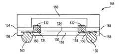
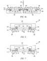
- FIG. 1shows a conventional Fo-WLCSP 10 including semiconductor die 12 having contact pads 14 and solder bumps 16 formed over active surface 18 .
- Semiconductor die 12is a flipchip type semiconductor die.
- An encapsulant 20is deposited over semiconductor die 12 and around bumps 16 .
- a build-up interconnect structure 22is formed over encapsulant 20 and semiconductor die 12 .
- the interconnect structure 22includes a conductive layer 24 and insulating layer 26 for electrical isolation of the conductive layer.
- Bumps 30are formed over conductive layer 24 .
- Wettable contact pads 28are typically formed between conductive layer 24 and bumps 16 to help contain the bump material during reflow.
- bumps 16are prone to cracking, particularly during thermal cycling test.
- bumps 16are known to delaminate from wettable contact pads 28 , and the wettable pads can delaminate from conductive layer 24 . The high temperature needed for bump reflow can subject the semiconductor wafer to degradation and damage.
- the present inventionis a method of making a semiconductor device comprising the steps of providing a semiconductor wafer having a plurality of semiconductor die with contact pads formed on an active surface of the semiconductor die, depositing a conductive polymer over the contact pads on the semiconductor wafer, singulating the semiconductor wafer to separate the semiconductor die, providing a carrier, forming a first insulating layer over the carrier, forming a plurality of openings in the first insulating layer, mounting the semiconductor die to the carrier with the conductive polymer disposed in the openings of the first insulating layer, heating the conductive polymer to a glass transition temperature, depositing an encapsulant over the semiconductor die and first insulating layer, removing the carrier to expose the conductive polymer, and forming an interconnect structure over the semiconductor die, encapsulant, and conductive polymer.
- the interconnect structureis electrically connected through
- the present inventionis a method of making a semiconductor device comprising the steps of providing a semiconductor die, depositing a conductive polymer over contact pads on the semiconductor die, providing a carrier, forming a first insulating layer over the carrier, forming a plurality of openings in the first insulating layer, mounting the semiconductor die to the carrier with the conductive polymer disposed in the openings of the first insulating layer, heating the conductive polymer to a glass transition temperature, depositing an encapsulant over the semiconductor die and first insulating layer, removing the carrier to expose the conductive polymer, and forming an interconnect structure over the semiconductor die, encapsulant, and conductive polymer.
- the interconnect structureis electrically connected through the conductive polymer to the contact pads on the semiconductor die.
- the present inventionis a method of making a semiconductor device comprising the steps of providing a semiconductor die, depositing a conductive polymer over contact pads on the semiconductor die, heating the conductive polymer to a glass transition temperature, depositing an encapsulant over the semiconductor die, and forming an interconnect structure over the semiconductor die, encapsulant, and conductive polymer.
- the interconnect structureis electrically connected through the conductive polymer to the contact pads on the semiconductor die.
- the present inventionis a semiconductor device comprising a semiconductor die and conductive polymer deposited over contact pads on the semiconductor die.
- the conductive polymeris heated to a glass transition temperature.
- An encapsulantis deposited over the semiconductor die.
- An interconnect structureis formed over the semiconductor die, encapsulant, and conductive polymer. The interconnect structure is electrically connected through the conductive polymer to the contact pads on the semiconductor die.
- FIG. 1illustrates a conventional Fo-WLCSP with a semiconductor die electrically connected to an interconnect structure through bumps and wettable contact pads;
- FIG. 2illustrates a PCB with different types of packages mounted to its surface
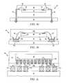
- FIGS. 3 a - 3 cillustrate further detail of the representative semiconductor packages mounted to the PCB
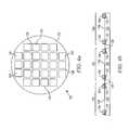
- FIGS. 4 a - 4 cillustrate a process of forming a conductive polymer over contact pads on a semiconductor wafer
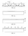
- FIGS. 5 a - 5 hillustrate a process of forming a Fo-WLCSP with b-stage conductive polymer formed over contact pads on the semiconductor die;
- FIG. 6illustrates the Fo-WLCSP with the b-stage conductive polymer electrically connecting the semiconductor die to the interconnect structure
- FIG. 7illustrates the Fo-WLCSP with the insulating layer remaining between the semiconductor die, encapsulant, and interconnect structure as a stress relief buffer.
- Front-end manufacturinginvolves the formation of a plurality of die on the surface of a semiconductor wafer.
- Each die on the wafercontains active and passive electrical components, which are electrically connected to form functional electrical circuits.
- Active electrical componentssuch as transistors and diodes, have the ability to control the flow of electrical current.
- Passive electrical componentssuch as capacitors, inductors, resistors, and transformers, create a relationship between voltage and current necessary to perform electrical circuit functions.
- Passive and active componentsare formed over the surface of the semiconductor wafer by a series of process steps including doping, deposition, photolithography, etching, and planarization.
- Dopingintroduces impurities into the semiconductor material by techniques such as ion implantation or thermal diffusion.
- the doping processmodifies the electrical conductivity of semiconductor material in active devices, transforming the semiconductor material into an insulator, conductor, or dynamically changing the semiconductor material conductivity in response to an electric field or base current.
- Transistorscontain regions of varying types and degrees of doping arranged as necessary to enable the transistor to promote or restrict the flow of electrical current upon the application of the electric field or base current.
- Active and passive componentsare formed by layers of materials with different electrical properties.
- the layerscan be formed by a variety of deposition techniques determined in part by the type of material being deposited. For example, thin film deposition may involve chemical vapor deposition (CVD), physical vapor deposition (PVD), electrolytic plating, and electroless plating processes.
- CVDchemical vapor deposition
- PVDphysical vapor deposition
- electrolytic platingelectroless plating processes.
- Each layeris generally patterned to form portions of active components, passive components, or electrical connections between components.
- the layerscan be patterned using photolithography, which involves the deposition of light sensitive material, e.g., photoresist, over the layer to be patterned.
- a patternis transferred from a photomask to the photoresist using light.
- the portion of the photoresist pattern subjected to lightis removed using a solvent, exposing portions of the underlying layer to be patterned.
- the remainder of the photoresistis removed, leaving behind a patterned layer.
- some types of materialsare patterned by directly depositing the material into the areas or voids formed by a previous deposition/etch process using techniques such as electroless and electrolytic plating.
- Planarizationcan be used to remove material from the surface of the wafer and produce a uniformly flat surface. Planarization involves polishing the surface of the wafer with a polishing pad. An abrasive material and corrosive chemical are added to the surface of the wafer during polishing. The combined mechanical action of the abrasive and corrosive action of the chemical removes any irregular topography, resulting in a uniformly flat surface.
- Back-end manufacturingrefers to cutting or singulating the finished wafer into the individual die and then packaging the die for structural support and environmental isolation.
- the waferis scored and broken along non-functional regions of the wafer called saw streets or scribes.
- the waferis singulated using a laser cutting tool or saw blade.
- the individual dieare mounted to a package substrate that includes pins or contact pads for interconnection with other system components.
- Contact pads formed over the semiconductor dieare then connected to contact pads within the package.
- the electrical connectionscan be made with solder bumps, stud bumps, conductive paste, or wirebonds.
- An encapsulant or other molding materialis deposited over the package to provide physical support and electrical isolation.
- the finished packageis then inserted into an electrical system and the functionality of the semiconductor device is made available to the other system components.
- FIG. 2illustrates electronic device 50 having a chip carrier substrate or printed circuit board (PCB) 52 with a plurality of semiconductor packages mounted on its surface.
- Electronic device 50may have one type of semiconductor package, or multiple types of semiconductor packages, depending on the application. The different types of semiconductor packages are shown in FIG. 2 for purposes of illustration.
- Electronic device 50may be a stand-alone system that uses the semiconductor packages to perform one or more electrical functions.
- electronic device 50may be a subcomponent of a larger system.
- electronic device 50may be part of a cellular phone, personal digital assistant (PDA), digital video camera (DVC), or other electronic communication device.
- PDApersonal digital assistant
- DVCdigital video camera
- electronic device 50can be a graphics card, network interface card, or other signal processing card that can be inserted into a computer.
- the semiconductor packagecan include microprocessors, memories, application specific integrated circuits (ASIC), logic circuits, analog circuits, RF circuits, discrete devices, or other semiconductor die or electrical components.
- ASICapplication specific integrated circuits
- the miniaturization and the weight reductionare essential for these products to be accepted by the market.
- the distance between semiconductor devicesmust be decreased to achieve higher density.
- PCB 52provides a general substrate for structural support and electrical interconnect of the semiconductor packages mounted on the PCB.
- Conductive signal traces 54are formed over a surface or within layers of PCB 52 using evaporation, electrolytic plating, electroless plating, screen printing, or other suitable metal deposition process. Signal traces 54 provide for electrical communication between each of the semiconductor packages, mounted components, and other external system components. Traces 54 also provide power and ground connections to each of the semiconductor packages.
- a semiconductor devicehas two packaging levels.
- First level packagingis a technique for mechanically and electrically attaching the semiconductor die to an intermediate carrier.
- Second level packaginginvolves mechanically and electrically attaching the intermediate carrier to the PCB.
- a semiconductor devicemay only have the first level packaging where the die is mechanically and electrically mounted directly to the PCB.
- first level packagingincluding wire bond package 56 and flip chip 58
- second level packagingincluding ball grid array (BGA) 60 , bump chip carrier (BCC) 62 , dual in-line package (DIP) 64 , land grid array (LGA) 66 , multi-chip module (MCM) 68 , quad flat non-leaded package (QFN) 70 , and quad flat package 72 .
- BGAball grid array
- BCCbump chip carrier
- DIPdual in-line package
- LGAland grid array
- MCMmulti-chip module
- QFNquad flat non-leaded package
- quad flat package 72quad flat package
- electronic device 50includes a single attached semiconductor package, while other embodiments call for multiple interconnected packages.
- manufacturerscan incorporate pre-made components into electronic devices and systems. Because the semiconductor packages include sophisticated functionality, electronic devices can be manufactured using cheaper components and a streamlined manufacturing process. The resulting devices are less likely to fail and less expensive to manufacture resulting in a lower cost for consumers.
- FIGS. 3 a - 3 cshow exemplary semiconductor packages.
- FIG. 3 aillustrates further detail of DIP 64 mounted on PCB 52 .
- Semiconductor die 74includes an active region containing analog or digital circuits implemented as active devices, passive devices, conductive layers, and dielectric layers formed within the die and are electrically interconnected according to the electrical design of the die.
- the circuitmay include one or more transistors, diodes, inductors, capacitors, resistors, and other circuit elements formed within the active region of semiconductor die 74 .
- Contact pads 76are one or more layers of conductive material, such as aluminum (Al), copper (Cu), tin (Sn), nickel (Ni), gold (Au), or silver (Ag), and are electrically connected to the circuit elements formed within semiconductor die 74 .
- semiconductor die 74is mounted to an intermediate carrier 78 using a gold-silicon eutectic layer or adhesive material such as thermal epoxy or epoxy resin.
- the package bodyincludes an insulative packaging material such as polymer or ceramic.
- Conductor leads 80 and wire bonds 82provide electrical interconnect between semiconductor die 74 and PCB 52 .
- Encapsulant 84is deposited over the package for environmental protection by preventing moisture and particles from entering the package and contaminating die 74 or wire bonds 82 .
- FIG. 3 billustrates further detail of BCC 62 mounted on PCB 52 .
- Semiconductor die 88is mounted over carrier 90 using an underfill or epoxy-resin adhesive material 92 .
- Wire bonds 94provide first level packaging interconnect between contact pads 96 and 98 .
- Molding compound or encapsulant 100is deposited over semiconductor die 88 and wire bonds 94 to provide physical support and electrical isolation for the device.
- Contact pads 102are formed over a surface of PCB 52 using a suitable metal deposition process such as electrolytic plating or electroless plating to prevent oxidation.
- Contact pads 102are electrically connected to one or more conductive signal traces 54 in PCB 52 .
- Bumps 104are formed between contact pads 98 of BCC 62 and contact pads 102 of PCB 52 .
- semiconductor die 58is mounted face down to intermediate carrier 106 with a flip chip style first level packaging.
- Active region 108 of semiconductor die 58contains analog or digital circuits implemented as active devices, passive devices, conductive layers, and dielectric layers formed according to the electrical design of the die.
- the circuitmay include one or more transistors, diodes, inductors, capacitors, resistors, and other circuit elements within active region 108 .
- Semiconductor die 58is electrically and mechanically connected to carrier 106 through bumps 110 .
- BGA 60is electrically and mechanically connected to PCB 52 with a BGA style second level packaging using bumps 112 .
- Semiconductor die 58is electrically connected to conductive signal traces 54 in PCB 52 through bumps 110 , signal lines 114 , and bumps 112 .
- a molding compound or encapsulant 116is deposited over semiconductor die 58 and carrier 106 to provide physical support and electrical isolation for the device.
- the flip chip semiconductor deviceprovides a short electrical conduction path from the active devices on semiconductor die 58 to conduction tracks on PCB 52 in order to reduce signal propagation distance, lower capacitance, and improve overall circuit performance.
- the semiconductor die 58can be mechanically and electrically connected directly to PCB 52 using flip chip style first level packaging without intermediate carrier 106 .
- FIG. 4 ashows a semiconductor wafer 120 with a base substrate material 122 , such as silicon, germanium, gallium arsenide, indium phosphide, or silicon carbide, for structural support.
- a plurality of semiconductor die or components 124is formed on wafer 120 separated by saw streets 126 as described above.
- FIG. 4 bshows a cross-sectional view of a portion of semiconductor wafer 120 .
- Each semiconductor die 124has an active surface 130 containing analog or digital circuits implemented as active devices, passive devices, conductive layers, and dielectric layers formed within the die and electrically interconnected according to the electrical design and function of the die.
- the circuitmay include one or more transistors, diodes, and other circuit elements formed within active surface 130 to implement analog circuits or digital circuits, such as digital signal processor (DSP), ASIC, memory, or other signal processing circuit.
- DSPdigital signal processor
- Semiconductor die 124may also contain IPDs, such as inductors, capacitors, and resistors, for RF signal processing.
- An electrically conductive layer 132is formed over active surface 130 using PVD, CVD, electrolytic plating, electroless plating process, or other suitable metal deposition process.
- Conductive layer 132can be one or more layers of Al, Cu, Sn, Ni, Au, Ag, or other suitable electrically conductive material.
- Conductive layer 132operates as contact pads electrically connected to the circuits on active surface 130 .
- semiconductor die 124is a flipchip type semiconductor die.
- a conductive polymer 134is deposited over contact pads 132 of semiconductor wafer 120 using low temperature lamination, screen printing, or other suitable application process.
- Conductive polymer 134is b-stage material, such as epoxy or acryl-based material with b-stage properties.
- conductive polymer 134contains metal particles or matrix of conductive particles, each having a polymer core with Ni plating and Au plating and outer polymer coating.
- Conductive polymer 134can also be implemented as carbon black, graphite, metals, and carbon nano-tubes.
- semiconductor wafer 120is singulated through saw street 126 using saw blade or laser cutting tool 136 into individual semiconductor die 124 .
- Each semiconductor die 124has conductive polymer 134 over contact pads 132 .
- FIGS. 5 a - 5 hillustrate, in relation to FIGS. 2 and 3 a - 3 c , a process of forming a Fo-WLCSP with a b-stage conductive polymer deposited over the contact pads of a semiconductor die.
- a temporary carrier or substrate 140contains sacrificial base material such as silicon, polymer, polymer composite, metal, ceramic, glass, glass epoxy, beryllium oxide, or other suitable low-cost, rigid material for structural support.
- An optional interface layer or double-sided tape 142can be formed over carrier 140 as a temporary adhesive bonding film or etch-stop layer.
- an insulating layer 144is formed over interface layer 142 as a mask layer using PVD, CVD, printing, spin coating, spray coating, sintering or thermal oxidation.
- the insulating layer 144can be photoresist material, dielectric material, epoxy resin, or underfill material.
- a portion of insulating layer 144is removed by an etching process to form openings or slots 146 which expose interface layer 142 .
- the openings 146are larger in width and depth than the volume of conductive polymer 134 formed on contact pads 132 .
- semiconductor die 124with conductive polymer 134 formed over contact pads 132 from FIGS. 4 a - 4 c , are mounted to carrier 140 with conductive polymer 134 disposed in openings 146 .
- the openings 146provide accurate alignment of individual semiconductor die 124 to carrier 140 , as well as reducing die shifting during encapsulation.
- conductive polymer 134After mounting semiconductor die 124 to carrier 140 with conductive polymer 134 disposed in openings 146 , conductive polymer 134 is heated to a glass transition temperature (T G ), such as 45-150° C., as necessary to liquefy and transform the conductive polymer to an electrically conductive state. Conductive polymer 134 completely fills openings 146 following the T G heating process.
- T Gglass transition temperature
- an encapsulant or molding compound 150is deposited over semiconductor die 124 and insulating layer 144 using a paste printing, compressive molding, transfer molding, liquid encapsulant molding, vacuum lamination, spin coating, or other suitable applicator.
- Encapsulant 150can be polymer composite material, such as epoxy resin with filler, epoxy acrylate with filler, or polymer with proper filler. Encapsulant 150 is non-conductive and environmentally protects the semiconductor device from external elements and contaminants.
- temporary carrier 140 , interface layer 142 , and insulating layer 144are removed by chemical etching, mechanical peel-off, CMP, mechanical grinding, thermal bake, UV light, laser scanning, or wet stripping.
- a build-up interconnect structure 152is formed over semiconductor die 124 , conductive polymer 134 , and encapsulant 150 .
- the build-up interconnect structure 152includes an insulating or passivation layer 154 formed using PVD, CVD, printing, spin coating, spray coating, sintering or thermal oxidation.
- the insulating layer 154contains one or more layers of silicon dioxide (SiO2), silicon nitride (Si3N4), silicon oxynitride (SiON), tantalum pentoxide (Ta2O5), aluminum oxide (Al2O3), or other material having similar insulating and structural properties. A portion of insulating layer 154 can be removed by an etching process if necessary to expose conductive polymer 134 .
- An electrically conductive layer or redistribution layer (RDL) 156is formed over insulating layer 154 using a patterning and metal deposition process such as sputtering, electrolytic plating, and electroless plating.
- Conductive layer 156can be one or more layers of Al, Cu, Sn, Ni, Au, Ag, or other suitable electrically conductive material.
- One portion of conductive layer 156is electrically connected to conductive polymer 134 .
- Other portions of conductive layer 156can be electrically common or electrically isolated depending on the design and function of semiconductor die 124 .
- An insulating or passivation layer 158is formed over insulating layer 154 and around conductive layer 156 using PVD, CVD, printing, spin coating, spray coating, sintering or thermal oxidation.
- the insulating layer 158contains one or more layers of SiO2, Si3N4, SiON, Ta2O5, Al2O3, or other material having similar insulating and structural properties. A portion of insulating layer 158 is removed by an etching process to expose conductive layer 156 .
- an electrically conductive bump materialis deposited over build-up interconnect structure 152 and electrically connected to the exposed portion of conductive layer 156 using an evaporation, electrolytic plating, electroless plating, ball drop, or screen printing process.
- the bump materialcan be Al, Sn, Ni, Au, Ag, Pb, Bi, Cu, solder, and combinations thereof, with an optional flux solution.
- the bump materialcan be eutectic Sn/Pb, high-lead solder, or lead-free solder.
- the bump materialis bonded to conductive layer 156 using a suitable attachment or bonding process. In one embodiment, the bump material is reflowed by heating the material above its melting point to form spherical balls or bumps 160 .
- bumps 160are reflowed a second time to improve electrical contact to conductive layer 156 .
- An under bump metallizationcan be formed under bumps 160 .
- the bumpscan also be compression bonded to conductive layer 156 .
- Bumps 160represent one type of interconnect structure that can be formed over conductive layer 156 .
- the interconnect structurecan also use stud bump, micro bump, or other electrical interconnect.
- Semiconductor die 124are singulated with saw blade or laser cutting tool 162 into individual Fo-WLCSP 164 .
- FIG. 6shows Fo-WLCSP 164 after singulation.
- Semiconductor die 124is electrically connected through contact pads 132 and conductive polymer 134 to build-up interconnect structure 152 and bumps 160 .
- Conductive polymer 134provides a simple and cost effective electrical connection between contact pads 132 and interconnect structure 152 .
- Conductive polymer 134negates the need for wettable contact pads and bumps, as described in FIG. 1 .
- FIG. 7shows an embodiment of Fo-WLCSP 166 , similar to FIG. 6 , with the exception that insulating layer 144 is not removed with carrier 140 in FIG. 5 f .
- the insulating layer 144remains as a stress relief buffer between semiconductor die 124 , encapsulant 150 , and interconnect structure 170 .
- a build-up interconnect structure 170is formed over conductive polymer 134 and insulating layer 144 .
- the build-up interconnect structure 170includes an electrically conductive layer or RDL 172 formed over insulating layer 144 using a patterning and metal deposition process such as sputtering, electrolytic plating, and electroless plating.
- Conductive layer 172can be one or more layers of Al, Cu, Sn, Ni, Au, Ag, or other suitable electrically conductive material.
- One portion of conductive layer 172is electrically connected through conductive polymer 134 .
- Other portions of conductive layer 172can be electrically common or electrically isolated depending on the design and function of semiconductor die 124 .
- An insulating or passivation layer 174is formed over insulating layer 144 and around conductive layer 172 using PVD, CVD, printing, spin coating, spray coating, sintering or thermal oxidation.
- the insulating layer 174contains one or more layers of SiO2, Si3N4, SiON, Ta2O5, Al2O3, or other material having similar insulating and structural properties. A portion of insulating layer 174 is removed by an etching process to expose conductive layer 172 .
- An electrically conductive bump materialis deposited over build-up interconnect structure 170 and electrically connected to the exposed portion of conductive layer 172 using an evaporation, electrolytic plating, electroless plating, ball drop, or screen printing process.
- the bump materialcan be Al, Sn, Ni, Au, Ag, Pb, Bi, Cu, solder, and combinations thereof, with an optional flux solution.
- the bump materialcan be eutectic Sn/Pb, high-lead solder, or lead-free solder.
- the bump materialis bonded to conductive layer 172 using a suitable attachment or bonding process. In one embodiment, the bump material is reflowed by heating the material above its melting point to form spherical balls or bumps 176 .
- bumps 176are reflowed a second time to improve electrical contact to conductive layer 172 .
- a UBMcan be formed under bumps 176 .
- the bumpscan also be compression bonded to conductive layer 172 .
- Bumps 176represent one type of interconnect structure that can be formed over conductive layer 172 .
- the interconnect structurecan also use stud bump, micro bump, or other electrical interconnect.
- Conductive polymer 134provides a simple and cost effective electrical connection between contact pads 132 and interconnect structure 170 . Conductive polymer 134 negates the need for wettable contact pads and bumps, as described in FIG. 1 .
Landscapes
- Engineering & Computer Science (AREA)
- Microelectronics & Electronic Packaging (AREA)
- Computer Hardware Design (AREA)
- Power Engineering (AREA)
- Physics & Mathematics (AREA)
- Condensed Matter Physics & Semiconductors (AREA)
- General Physics & Mathematics (AREA)
- Manufacturing & Machinery (AREA)
- Internal Circuitry In Semiconductor Integrated Circuit Devices (AREA)
- Encapsulation Of And Coatings For Semiconductor Or Solid State Devices (AREA)
Abstract
Description
- The present invention relates in general to semiconductor devices and, more particularly, to a semiconductor device and method of forming a b-stage conductive polymer over contact pads of a semiconductor die in a fan-out wafer level chip scale package (Fo-WLCSP).
- Semiconductor devices are commonly found in modern electronic products. Semiconductor devices vary in the number and density of electrical components. Discrete semiconductor devices generally contain one type of electrical component, e.g., light emitting diode (LED), small signal transistor, resistor, capacitor, inductor, and power metal oxide semiconductor field effect transistor (MOSFET). Integrated semiconductor devices typically contain hundreds to millions of electrical components. Examples of integrated semiconductor devices include microcontrollers, microprocessors, charged-coupled devices (CCDs), solar cells, and digital micro-mirror devices (DMDs).
- Semiconductor devices perform a wide range of functions such as signal processing, high-speed calculations, transmitting and receiving electromagnetic signals, controlling electronic devices, transforming sunlight to electricity, and creating visual projections for television displays. Semiconductor devices are found in the fields of entertainment, communications, power conversion, networks, computers, and consumer products. Semiconductor devices are also found in military applications, aviation, automotive, industrial controllers, and office equipment.
- Semiconductor devices exploit the electrical properties of semiconductor materials. The atomic structure of semiconductor material allows its electrical conductivity to be manipulated by the application of an electric field or base current or through the process of doping. Doping introduces impurities into the semiconductor material to manipulate and control the conductivity of the semiconductor device.
- A semiconductor device contains active and passive electrical structures. Active structures, including bipolar and field effect transistors, control the flow of electrical current. By varying levels of doping and application of an electric field or base current, the transistor either promotes or restricts the flow of electrical current. Passive structures, including resistors, capacitors, and inductors, create a relationship between voltage and current necessary to perform a variety of electrical functions. The passive and active structures are electrically connected to form circuits, which enable the semiconductor device to perform high-speed calculations and other useful functions.
- Semiconductor devices are generally manufactured using two complex manufacturing processes, i.e., front-end manufacturing, and back-end manufacturing, each involving potentially hundreds of steps. Front-end manufacturing involves the formation of a plurality of die on the surface of a semiconductor wafer. Each die is typically identical and contains circuits formed by electrically connecting active and passive components. Back-end manufacturing involves singulating individual die from the finished wafer and packaging the die to provide structural support and environmental isolation.
- One goal of semiconductor manufacturing is to produce smaller semiconductor devices. Smaller devices typically consume less power, have higher performance, and can be produced more efficiently. In addition, smaller semiconductor devices have a smaller footprint, which is desirable for smaller end products. A smaller die size may be achieved by improvements in the front-end process resulting in die with smaller, higher density active and passive components. Back-end processes may result in semiconductor device packages with a smaller footprint by improvements in electrical interconnection and packaging materials.
FIG. 1 shows a conventional Fo-WLCSP10 includingsemiconductor die 12 having contact pads14 and solder bumps16 formed over active surface18. Semiconductor die12 is a flipchip type semiconductor die. An encapsulant20 is deposited over semiconductor die12 and around bumps16. A build-up interconnect structure22 is formed over encapsulant20 and semiconductor die12. The interconnect structure22 includes a conductive layer24 and insulating layer26 for electrical isolation of the conductive layer. Bumps30 are formed over conductive layer24.- Many semiconductor devices require a fine pitch between the interconnect structures, e.g., between contact pads on a flipchip semiconductor die, for a high interconnect density and input/output (I/O) terminal count. Wettable contact pads28 are typically formed between conductive layer24 and bumps16 to help contain the bump material during reflow. However, bumps16 are prone to cracking, particularly during thermal cycling test. In addition, bumps16 are known to delaminate from wettable contact pads28, and the wettable pads can delaminate from conductive layer24. The high temperature needed for bump reflow can subject the semiconductor wafer to degradation and damage.
- A need exists to provide a fine pitch interconnect for a semiconductor die without using bumps and wettable contact pads to electrically interconnect the semiconductor die. Accordingly, in one embodiment, the present invention is a method of making a semiconductor device comprising the steps of providing a semiconductor wafer having a plurality of semiconductor die with contact pads formed on an active surface of the semiconductor die, depositing a conductive polymer over the contact pads on the semiconductor wafer, singulating the semiconductor wafer to separate the semiconductor die, providing a carrier, forming a first insulating layer over the carrier, forming a plurality of openings in the first insulating layer, mounting the semiconductor die to the carrier with the conductive polymer disposed in the openings of the first insulating layer, heating the conductive polymer to a glass transition temperature, depositing an encapsulant over the semiconductor die and first insulating layer, removing the carrier to expose the conductive polymer, and forming an interconnect structure over the semiconductor die, encapsulant, and conductive polymer. The interconnect structure is electrically connected through the conductive polymer to the contact pads on the semiconductor die.
- In another embodiment, the present invention is a method of making a semiconductor device comprising the steps of providing a semiconductor die, depositing a conductive polymer over contact pads on the semiconductor die, providing a carrier, forming a first insulating layer over the carrier, forming a plurality of openings in the first insulating layer, mounting the semiconductor die to the carrier with the conductive polymer disposed in the openings of the first insulating layer, heating the conductive polymer to a glass transition temperature, depositing an encapsulant over the semiconductor die and first insulating layer, removing the carrier to expose the conductive polymer, and forming an interconnect structure over the semiconductor die, encapsulant, and conductive polymer. The interconnect structure is electrically connected through the conductive polymer to the contact pads on the semiconductor die.
- In another embodiment, the present invention is a method of making a semiconductor device comprising the steps of providing a semiconductor die, depositing a conductive polymer over contact pads on the semiconductor die, heating the conductive polymer to a glass transition temperature, depositing an encapsulant over the semiconductor die, and forming an interconnect structure over the semiconductor die, encapsulant, and conductive polymer. The interconnect structure is electrically connected through the conductive polymer to the contact pads on the semiconductor die.
- In another embodiment, the present invention is a semiconductor device comprising a semiconductor die and conductive polymer deposited over contact pads on the semiconductor die. The conductive polymer is heated to a glass transition temperature. An encapsulant is deposited over the semiconductor die. An interconnect structure is formed over the semiconductor die, encapsulant, and conductive polymer. The interconnect structure is electrically connected through the conductive polymer to the contact pads on the semiconductor die.
FIG. 1 illustrates a conventional Fo-WLCSP with a semiconductor die electrically connected to an interconnect structure through bumps and wettable contact pads;FIG. 2 illustrates a PCB with different types of packages mounted to its surface;FIGS. 3 a-3cillustrate further detail of the representative semiconductor packages mounted to the PCB;FIGS. 4 a-4cillustrate a process of forming a conductive polymer over contact pads on a semiconductor wafer;FIGS. 5 a-5hillustrate a process of forming a Fo-WLCSP with b-stage conductive polymer formed over contact pads on the semiconductor die;FIG. 6 illustrates the Fo-WLCSP with the b-stage conductive polymer electrically connecting the semiconductor die to the interconnect structure; andFIG. 7 illustrates the Fo-WLCSP with the insulating layer remaining between the semiconductor die, encapsulant, and interconnect structure as a stress relief buffer.- The present invention is described in one or more embodiments in the following description with reference to the figures, in which like numerals represent the same or similar elements. While the invention is described in terms of the best mode for achieving the invention's objectives, it will be appreciated by those skilled in the art that it is intended to cover alternatives, modifications, and equivalents as may be included within the spirit and scope of the invention as defined by the appended claims and their equivalents as supported by the following disclosure and drawings.
- Semiconductor devices are generally manufactured using two complex manufacturing processes: front-end manufacturing and back-end manufacturing. Front-end manufacturing involves the formation of a plurality of die on the surface of a semiconductor wafer. Each die on the wafer contains active and passive electrical components, which are electrically connected to form functional electrical circuits. Active electrical components, such as transistors and diodes, have the ability to control the flow of electrical current. Passive electrical components, such as capacitors, inductors, resistors, and transformers, create a relationship between voltage and current necessary to perform electrical circuit functions.
- Passive and active components are formed over the surface of the semiconductor wafer by a series of process steps including doping, deposition, photolithography, etching, and planarization. Doping introduces impurities into the semiconductor material by techniques such as ion implantation or thermal diffusion. The doping process modifies the electrical conductivity of semiconductor material in active devices, transforming the semiconductor material into an insulator, conductor, or dynamically changing the semiconductor material conductivity in response to an electric field or base current. Transistors contain regions of varying types and degrees of doping arranged as necessary to enable the transistor to promote or restrict the flow of electrical current upon the application of the electric field or base current.
- Active and passive components are formed by layers of materials with different electrical properties. The layers can be formed by a variety of deposition techniques determined in part by the type of material being deposited. For example, thin film deposition may involve chemical vapor deposition (CVD), physical vapor deposition (PVD), electrolytic plating, and electroless plating processes. Each layer is generally patterned to form portions of active components, passive components, or electrical connections between components.
- The layers can be patterned using photolithography, which involves the deposition of light sensitive material, e.g., photoresist, over the layer to be patterned. A pattern is transferred from a photomask to the photoresist using light. The portion of the photoresist pattern subjected to light is removed using a solvent, exposing portions of the underlying layer to be patterned. The remainder of the photoresist is removed, leaving behind a patterned layer. Alternatively, some types of materials are patterned by directly depositing the material into the areas or voids formed by a previous deposition/etch process using techniques such as electroless and electrolytic plating.
- Depositing a thin film of material over an existing pattern can exaggerate the underlying pattern and create a non-uniformly flat surface. A uniformly flat surface is required to produce smaller and more densely packed active and passive components. Planarization can be used to remove material from the surface of the wafer and produce a uniformly flat surface. Planarization involves polishing the surface of the wafer with a polishing pad. An abrasive material and corrosive chemical are added to the surface of the wafer during polishing. The combined mechanical action of the abrasive and corrosive action of the chemical removes any irregular topography, resulting in a uniformly flat surface.
- Back-end manufacturing refers to cutting or singulating the finished wafer into the individual die and then packaging the die for structural support and environmental isolation. To singulate the die, the wafer is scored and broken along non-functional regions of the wafer called saw streets or scribes. The wafer is singulated using a laser cutting tool or saw blade. After singulation, the individual die are mounted to a package substrate that includes pins or contact pads for interconnection with other system components. Contact pads formed over the semiconductor die are then connected to contact pads within the package. The electrical connections can be made with solder bumps, stud bumps, conductive paste, or wirebonds. An encapsulant or other molding material is deposited over the package to provide physical support and electrical isolation. The finished package is then inserted into an electrical system and the functionality of the semiconductor device is made available to the other system components.
FIG. 2 illustrates electronic device50 having a chip carrier substrate or printed circuit board (PCB)52 with a plurality of semiconductor packages mounted on its surface. Electronic device50 may have one type of semiconductor package, or multiple types of semiconductor packages, depending on the application. The different types of semiconductor packages are shown inFIG. 2 for purposes of illustration.- Electronic device50 may be a stand-alone system that uses the semiconductor packages to perform one or more electrical functions. Alternatively, electronic device50 may be a subcomponent of a larger system. For example, electronic device50 may be part of a cellular phone, personal digital assistant (PDA), digital video camera (DVC), or other electronic communication device. Alternatively, electronic device50 can be a graphics card, network interface card, or other signal processing card that can be inserted into a computer. The semiconductor package can include microprocessors, memories, application specific integrated circuits (ASIC), logic circuits, analog circuits, RF circuits, discrete devices, or other semiconductor die or electrical components. The miniaturization and the weight reduction are essential for these products to be accepted by the market. The distance between semiconductor devices must be decreased to achieve higher density.
- In
FIG. 2 ,PCB 52 provides a general substrate for structural support and electrical interconnect of the semiconductor packages mounted on the PCB. Conductive signal traces54 are formed over a surface or within layers ofPCB 52 using evaporation, electrolytic plating, electroless plating, screen printing, or other suitable metal deposition process. Signal traces54 provide for electrical communication between each of the semiconductor packages, mounted components, and other external system components. Traces54 also provide power and ground connections to each of the semiconductor packages. - In some embodiments, a semiconductor device has two packaging levels. First level packaging is a technique for mechanically and electrically attaching the semiconductor die to an intermediate carrier. Second level packaging involves mechanically and electrically attaching the intermediate carrier to the PCB. In other embodiments, a semiconductor device may only have the first level packaging where the die is mechanically and electrically mounted directly to the PCB.
- For the purpose of illustration, several types of first level packaging, including wire bond package56 and
flip chip 58, are shown onPCB 52. Additionally, several types of second level packaging, including ball grid array (BGA)60, bump chip carrier (BCC)62, dual in-line package (DIP)64, land grid array (LGA)66, multi-chip module (MCM)68, quad flat non-leaded package (QFN)70, and quad flat package72, are shown mounted onPCB 52. Depending upon the system requirements, any combination of semiconductor packages, configured with any combination of first and second level packaging styles, as well as other electronic components, can be connected toPCB 52. In some embodiments, electronic device50 includes a single attached semiconductor package, while other embodiments call for multiple interconnected packages. By combining one or more semiconductor packages over a single substrate, manufacturers can incorporate pre-made components into electronic devices and systems. Because the semiconductor packages include sophisticated functionality, electronic devices can be manufactured using cheaper components and a streamlined manufacturing process. The resulting devices are less likely to fail and less expensive to manufacture resulting in a lower cost for consumers. FIGS. 3 a-3cshow exemplary semiconductor packages.FIG. 3 aillustrates further detail ofDIP 64 mounted onPCB 52. Semiconductor die74 includes an active region containing analog or digital circuits implemented as active devices, passive devices, conductive layers, and dielectric layers formed within the die and are electrically interconnected according to the electrical design of the die. For example, the circuit may include one or more transistors, diodes, inductors, capacitors, resistors, and other circuit elements formed within the active region of semiconductor die74. Contactpads 76 are one or more layers of conductive material, such as aluminum (Al), copper (Cu), tin (Sn), nickel (Ni), gold (Au), or silver (Ag), and are electrically connected to the circuit elements formed within semiconductor die74. During assembly ofDIP 64, semiconductor die74 is mounted to anintermediate carrier 78 using a gold-silicon eutectic layer or adhesive material such as thermal epoxy or epoxy resin. The package body includes an insulative packaging material such as polymer or ceramic. Conductor leads80 andwire bonds 82 provide electrical interconnect between semiconductor die74 andPCB 52.Encapsulant 84 is deposited over the package for environmental protection by preventing moisture and particles from entering the package and contaminating die74 or wire bonds82.FIG. 3 billustrates further detail ofBCC 62 mounted onPCB 52. Semiconductor die88 is mounted overcarrier 90 using an underfill or epoxy-resin adhesive material 92.Wire bonds 94 provide first level packaging interconnect betweencontact pads encapsulant 100 is deposited over semiconductor die88 andwire bonds 94 to provide physical support and electrical isolation for the device. Contactpads 102 are formed over a surface ofPCB 52 using a suitable metal deposition process such as electrolytic plating or electroless plating to prevent oxidation. Contactpads 102 are electrically connected to one or more conductive signal traces54 inPCB 52.Bumps 104 are formed betweencontact pads 98 ofBCC 62 andcontact pads 102 ofPCB 52.- In
FIG. 3 c, semiconductor die58 is mounted face down tointermediate carrier 106 with a flip chip style first level packaging.Active region 108 of semiconductor die58 contains analog or digital circuits implemented as active devices, passive devices, conductive layers, and dielectric layers formed according to the electrical design of the die. For example, the circuit may include one or more transistors, diodes, inductors, capacitors, resistors, and other circuit elements withinactive region 108. Semiconductor die58 is electrically and mechanically connected tocarrier 106 throughbumps 110. BGA 60 is electrically and mechanically connected toPCB 52 with a BGA style second levelpackaging using bumps 112. Semiconductor die58 is electrically connected to conductive signal traces54 inPCB 52 throughbumps 110,signal lines 114, and bumps112. A molding compound orencapsulant 116 is deposited over semiconductor die58 andcarrier 106 to provide physical support and electrical isolation for the device. The flip chip semiconductor device provides a short electrical conduction path from the active devices on semiconductor die58 to conduction tracks onPCB 52 in order to reduce signal propagation distance, lower capacitance, and improve overall circuit performance. In another embodiment, the semiconductor die58 can be mechanically and electrically connected directly toPCB 52 using flip chip style first level packaging withoutintermediate carrier 106.FIG. 4 ashows asemiconductor wafer 120 with abase substrate material 122, such as silicon, germanium, gallium arsenide, indium phosphide, or silicon carbide, for structural support. A plurality of semiconductor die orcomponents 124 is formed onwafer 120 separated by sawstreets 126 as described above.FIG. 4 bshows a cross-sectional view of a portion ofsemiconductor wafer 120. Each semiconductor die124 has anactive surface 130 containing analog or digital circuits implemented as active devices, passive devices, conductive layers, and dielectric layers formed within the die and electrically interconnected according to the electrical design and function of the die. For example, the circuit may include one or more transistors, diodes, and other circuit elements formed withinactive surface 130 to implement analog circuits or digital circuits, such as digital signal processor (DSP), ASIC, memory, or other signal processing circuit. Semiconductor die124 may also contain IPDs, such as inductors, capacitors, and resistors, for RF signal processing.- An electrically
conductive layer 132 is formed overactive surface 130 using PVD, CVD, electrolytic plating, electroless plating process, or other suitable metal deposition process.Conductive layer 132 can be one or more layers of Al, Cu, Sn, Ni, Au, Ag, or other suitable electrically conductive material.Conductive layer 132 operates as contact pads electrically connected to the circuits onactive surface 130. In one embodiment, semiconductor die124 is a flipchip type semiconductor die. - A
conductive polymer 134 is deposited overcontact pads 132 ofsemiconductor wafer 120 using low temperature lamination, screen printing, or other suitable application process.Conductive polymer 134 is b-stage material, such as epoxy or acryl-based material with b-stage properties. In one embodiment,conductive polymer 134 contains metal particles or matrix of conductive particles, each having a polymer core with Ni plating and Au plating and outer polymer coating.Conductive polymer 134 can also be implemented as carbon black, graphite, metals, and carbon nano-tubes. - In
FIG. 4 c,semiconductor wafer 120 is singulated throughsaw street 126 using saw blade orlaser cutting tool 136 into individual semiconductor die124. Each semiconductor die124 hasconductive polymer 134 overcontact pads 132. FIGS. 5 a-5hillustrate, in relation toFIGS. 2 and 3 a-3c, a process of forming a Fo-WLCSP with a b-stage conductive polymer deposited over the contact pads of a semiconductor die. InFIG. 5 a, a temporary carrier orsubstrate 140 contains sacrificial base material such as silicon, polymer, polymer composite, metal, ceramic, glass, glass epoxy, beryllium oxide, or other suitable low-cost, rigid material for structural support. An optional interface layer or double-sided tape 142 can be formed overcarrier 140 as a temporary adhesive bonding film or etch-stop layer.- In
FIG. 5 b, an insulatinglayer 144 is formed overinterface layer 142 as a mask layer using PVD, CVD, printing, spin coating, spray coating, sintering or thermal oxidation. The insulatinglayer 144 can be photoresist material, dielectric material, epoxy resin, or underfill material. - In
FIG. 5 c, a portion of insulatinglayer 144 is removed by an etching process to form openings orslots 146 which exposeinterface layer 142. Theopenings 146 are larger in width and depth than the volume ofconductive polymer 134 formed oncontact pads 132. - In
FIG. 5 d, semiconductor die124, withconductive polymer 134 formed overcontact pads 132 fromFIGS. 4 a-4c, are mounted tocarrier 140 withconductive polymer 134 disposed inopenings 146. Theopenings 146 provide accurate alignment of individual semiconductor die124 tocarrier 140, as well as reducing die shifting during encapsulation. - After mounting semiconductor die124 to
carrier 140 withconductive polymer 134 disposed inopenings 146,conductive polymer 134 is heated to a glass transition temperature (TG), such as 45-150° C., as necessary to liquefy and transform the conductive polymer to an electrically conductive state.Conductive polymer 134 completely fillsopenings 146 following the TGheating process. - In
FIG. 5 e, an encapsulant ormolding compound 150 is deposited over semiconductor die124 and insulatinglayer 144 using a paste printing, compressive molding, transfer molding, liquid encapsulant molding, vacuum lamination, spin coating, or other suitable applicator.Encapsulant 150 can be polymer composite material, such as epoxy resin with filler, epoxy acrylate with filler, or polymer with proper filler.Encapsulant 150 is non-conductive and environmentally protects the semiconductor device from external elements and contaminants. - In
FIG. 5 f,temporary carrier 140,interface layer 142, and insulatinglayer 144 are removed by chemical etching, mechanical peel-off, CMP, mechanical grinding, thermal bake, UV light, laser scanning, or wet stripping. - In
FIG. 5 g, a build-upinterconnect structure 152 is formed over semiconductor die124,conductive polymer 134, andencapsulant 150. The build-upinterconnect structure 152 includes an insulating orpassivation layer 154 formed using PVD, CVD, printing, spin coating, spray coating, sintering or thermal oxidation. The insulatinglayer 154 contains one or more layers of silicon dioxide (SiO2), silicon nitride (Si3N4), silicon oxynitride (SiON), tantalum pentoxide (Ta2O5), aluminum oxide (Al2O3), or other material having similar insulating and structural properties. A portion of insulatinglayer 154 can be removed by an etching process if necessary to exposeconductive polymer 134. - An electrically conductive layer or redistribution layer (RDL)156 is formed over
insulating layer 154 using a patterning and metal deposition process such as sputtering, electrolytic plating, and electroless plating.Conductive layer 156 can be one or more layers of Al, Cu, Sn, Ni, Au, Ag, or other suitable electrically conductive material. One portion ofconductive layer 156 is electrically connected toconductive polymer 134. Other portions ofconductive layer 156 can be electrically common or electrically isolated depending on the design and function of semiconductor die124. - An insulating or
passivation layer 158 is formed overinsulating layer 154 and aroundconductive layer 156 using PVD, CVD, printing, spin coating, spray coating, sintering or thermal oxidation. The insulatinglayer 158 contains one or more layers of SiO2, Si3N4, SiON, Ta2O5, Al2O3, or other material having similar insulating and structural properties. A portion of insulatinglayer 158 is removed by an etching process to exposeconductive layer 156. - In
FIG. 5 h, an electrically conductive bump material is deposited over build-upinterconnect structure 152 and electrically connected to the exposed portion ofconductive layer 156 using an evaporation, electrolytic plating, electroless plating, ball drop, or screen printing process. The bump material can be Al, Sn, Ni, Au, Ag, Pb, Bi, Cu, solder, and combinations thereof, with an optional flux solution. For example, the bump material can be eutectic Sn/Pb, high-lead solder, or lead-free solder. The bump material is bonded toconductive layer 156 using a suitable attachment or bonding process. In one embodiment, the bump material is reflowed by heating the material above its melting point to form spherical balls or bumps160. In some applications, bumps160 are reflowed a second time to improve electrical contact toconductive layer 156. An under bump metallization (UBM) can be formed underbumps 160. The bumps can also be compression bonded toconductive layer 156.Bumps 160 represent one type of interconnect structure that can be formed overconductive layer 156. The interconnect structure can also use stud bump, micro bump, or other electrical interconnect. - Semiconductor die124 are singulated with saw blade or
laser cutting tool 162 into individual Fo-WLCSP 164.FIG. 6 shows Fo-WLCSP 164 after singulation. Semiconductor die124 is electrically connected throughcontact pads 132 andconductive polymer 134 to build-upinterconnect structure 152 and bumps160.Conductive polymer 134 provides a simple and cost effective electrical connection betweencontact pads 132 andinterconnect structure 152.Conductive polymer 134 negates the need for wettable contact pads and bumps, as described inFIG. 1 . FIG. 7 shows an embodiment of Fo-WLCSP 166, similar toFIG. 6 , with the exception that insulatinglayer 144 is not removed withcarrier 140 inFIG. 5 f. The insulatinglayer 144 remains as a stress relief buffer between semiconductor die124,encapsulant 150, andinterconnect structure 170.- A build-up
interconnect structure 170 is formed overconductive polymer 134 and insulatinglayer 144. The build-upinterconnect structure 170 includes an electrically conductive layer orRDL 172 formed overinsulating layer 144 using a patterning and metal deposition process such as sputtering, electrolytic plating, and electroless plating.Conductive layer 172 can be one or more layers of Al, Cu, Sn, Ni, Au, Ag, or other suitable electrically conductive material. One portion ofconductive layer 172 is electrically connected throughconductive polymer 134. Other portions ofconductive layer 172 can be electrically common or electrically isolated depending on the design and function of semiconductor die124. - An insulating or
passivation layer 174 is formed overinsulating layer 144 and aroundconductive layer 172 using PVD, CVD, printing, spin coating, spray coating, sintering or thermal oxidation. The insulatinglayer 174 contains one or more layers of SiO2, Si3N4, SiON, Ta2O5, Al2O3, or other material having similar insulating and structural properties. A portion of insulatinglayer 174 is removed by an etching process to exposeconductive layer 172. - An electrically conductive bump material is deposited over build-up
interconnect structure 170 and electrically connected to the exposed portion ofconductive layer 172 using an evaporation, electrolytic plating, electroless plating, ball drop, or screen printing process. The bump material can be Al, Sn, Ni, Au, Ag, Pb, Bi, Cu, solder, and combinations thereof, with an optional flux solution. For example, the bump material can be eutectic Sn/Pb, high-lead solder, or lead-free solder. The bump material is bonded toconductive layer 172 using a suitable attachment or bonding process. In one embodiment, the bump material is reflowed by heating the material above its melting point to form spherical balls or bumps176. In some applications, bumps176 are reflowed a second time to improve electrical contact toconductive layer 172. A UBM can be formed underbumps 176. The bumps can also be compression bonded toconductive layer 172.Bumps 176 represent one type of interconnect structure that can be formed overconductive layer 172. The interconnect structure can also use stud bump, micro bump, or other electrical interconnect. - Semiconductor die124 is electrically connected through
contact pads 132 andconductive polymer 134 to build-upinterconnect structure 170 and bumps176.Conductive polymer 134 provides a simple and cost effective electrical connection betweencontact pads 132 andinterconnect structure 170.Conductive polymer 134 negates the need for wettable contact pads and bumps, as described inFIG. 1 . - While one or more embodiments of the present invention have been illustrated in detail, the skilled artisan will appreciate that modifications and adaptations to those embodiments may be made without departing from the scope of the present invention as set forth in the following claims.
Claims (25)
Priority Applications (2)
| Application Number | Priority Date | Filing Date | Title |
|---|---|---|---|
| US12/853,898US8193610B2 (en) | 2010-08-10 | 2010-08-10 | Semiconductor device and method of forming B-stage conductive polymer over contact pads of semiconductor die in Fo-WLCSP |
| US13/438,713US9418941B2 (en) | 2010-08-10 | 2012-04-03 | Semiconductor device and method of forming B-stage conductive polymer over contact pads of semiconductor die in Fo-WLCSP |
Applications Claiming Priority (1)
| Application Number | Priority Date | Filing Date | Title |
|---|---|---|---|
| US12/853,898US8193610B2 (en) | 2010-08-10 | 2010-08-10 | Semiconductor device and method of forming B-stage conductive polymer over contact pads of semiconductor die in Fo-WLCSP |
Related Child Applications (1)
| Application Number | Title | Priority Date | Filing Date |
|---|---|---|---|
| US13/438,713DivisionUS9418941B2 (en) | 2010-08-10 | 2012-04-03 | Semiconductor device and method of forming B-stage conductive polymer over contact pads of semiconductor die in Fo-WLCSP |
Publications (2)
| Publication Number | Publication Date |
|---|---|
| US20120038047A1true US20120038047A1 (en) | 2012-02-16 |
| US8193610B2 US8193610B2 (en) | 2012-06-05 |
Family
ID=45564234
Family Applications (2)
| Application Number | Title | Priority Date | Filing Date |
|---|---|---|---|
| US12/853,898Active2030-11-03US8193610B2 (en) | 2010-08-10 | 2010-08-10 | Semiconductor device and method of forming B-stage conductive polymer over contact pads of semiconductor die in Fo-WLCSP |
| US13/438,713Active2031-03-08US9418941B2 (en) | 2010-08-10 | 2012-04-03 | Semiconductor device and method of forming B-stage conductive polymer over contact pads of semiconductor die in Fo-WLCSP |
Family Applications After (1)
| Application Number | Title | Priority Date | Filing Date |
|---|---|---|---|
| US13/438,713Active2031-03-08US9418941B2 (en) | 2010-08-10 | 2012-04-03 | Semiconductor device and method of forming B-stage conductive polymer over contact pads of semiconductor die in Fo-WLCSP |
Country Status (1)
| Country | Link |
|---|---|
| US (2) | US8193610B2 (en) |
Cited By (20)
| Publication number | Priority date | Publication date | Assignee | Title |
|---|---|---|---|---|
| US20120112336A1 (en)* | 2010-11-05 | 2012-05-10 | Guzek John S | Encapsulated die, microelectronic package containing same, and method of manufacturing said microelectronic package |
| US20130147037A1 (en)* | 2011-12-09 | 2013-06-13 | Chipmos Technologies Inc. | Semiconductor structure |
| US20130187178A1 (en)* | 2012-01-24 | 2013-07-25 | Michael A. Tischler | Light-emitting dies incorporating wavelength-conversion materials and related methods |
| US8569886B2 (en)* | 2011-11-22 | 2013-10-29 | Taiwan Semiconductor Manufacturing Company, Ltd. | Methods and apparatus of under bump metallization in packaging semiconductor devices |
| US20140091482A1 (en)* | 2012-10-02 | 2014-04-03 | Stats Chippac, Ltd. | Semiconductor Device and Method of Depositing Encapsulant Along Sides and Surface Edge of Semiconductor Die in Embedded WLCSP |
| EP2830091A1 (en)* | 2013-07-23 | 2015-01-28 | Grote Industries, LLC | Flexible lighting device having unobtrusive conductive layers |
| EP2830090A1 (en)* | 2013-07-23 | 2015-01-28 | Grote Industries, LLC | Flexible lighting device having unobtrusive conductive layers |
| US9190581B2 (en) | 2012-01-24 | 2015-11-17 | Cooledge Lighting Inc. | Light-emitting dies incorporating wavelength-conversion materials and related methods |
| US20160005705A1 (en)* | 2014-07-01 | 2016-01-07 | Texas Instruments Incorporated | Structure and Method of Batch-Packaging Low Pin Count Embedded Semiconductor Chips |
| US9236502B2 (en) | 2012-01-24 | 2016-01-12 | Cooledge Lighting, Inc. | Wafer-level flip chip device packages and related methods |
| WO2016060676A1 (en)* | 2014-10-17 | 2016-04-21 | Intel Corporation | Microled display & assembly |
| US9343443B2 (en) | 2014-02-05 | 2016-05-17 | Cooledge Lighting, Inc. | Light-emitting dies incorporating wavelength-conversion materials and related methods |
| JP2017055024A (en)* | 2015-09-11 | 2017-03-16 | Shマテリアル株式会社 | Semiconductor element mounting substrate, semiconductor device, and manufacturing methods thereof |
| US9620413B2 (en) | 2012-10-02 | 2017-04-11 | STATS ChipPAC Pte. Ltd. | Semiconductor device and method of using a standardized carrier in semiconductor packaging |
| US10658330B2 (en) | 2013-01-03 | 2020-05-19 | STATS ChipPAC Pte. Ltd. | Semiconductor device and method of using a standardized carrier to form embedded wafer level chip scale packages |
| US10777528B2 (en) | 2013-01-03 | 2020-09-15 | STATS ChipPAC Pte. Ltd. | Semiconductor device and method of forming embedded wafer level chip scale packages |
| US10886153B2 (en) | 2014-10-17 | 2021-01-05 | Intel Corporation | Display including an LED element having a pressure sensitive adhesive (PSA) for micro pick and bond assembly of the display |
| US11450620B2 (en)* | 2018-05-02 | 2022-09-20 | Intel Corporation | Innovative fan-out panel level package (FOPLP) warpage control |
| US20220359338A1 (en)* | 2021-05-06 | 2022-11-10 | Qualcomm Technologies, Inc. | High-power die heat sink with vertical heat path |
| US11948853B2 (en) | 2021-05-06 | 2024-04-02 | QUALCOMM Technologies Incorporated | High-power die heat sink |
Families Citing this family (2)
| Publication number | Priority date | Publication date | Assignee | Title |
|---|---|---|---|---|
| US9418877B2 (en)* | 2014-05-05 | 2016-08-16 | Qualcomm Incorporated | Integrated device comprising high density interconnects in inorganic layers and redistribution layers in organic layers |
| US9496234B1 (en) | 2015-06-17 | 2016-11-15 | Globalfoundries Inc. | Wafer-level chip-scale package structure utilizing conductive polymer |
Citations (3)
| Publication number | Priority date | Publication date | Assignee | Title |
|---|---|---|---|---|
| US20030137062A1 (en)* | 1996-09-20 | 2003-07-24 | Salman Akram | Use of nitrides for flip-chip encapsulation |
| US6797544B2 (en)* | 2000-10-20 | 2004-09-28 | Matsushita Electric Industrial Co., Ltd. | Semiconductor device, method of manufacturing the device and method of mounting the device |
| US7800233B2 (en)* | 2005-07-26 | 2010-09-21 | Nec Electronics Corporation | Semiconductor device and method of manufacturing the same |
Family Cites Families (16)
| Publication number | Priority date | Publication date | Assignee | Title |
|---|---|---|---|---|
| US5043845A (en)* | 1989-10-16 | 1991-08-27 | Eastman Kodak Company | High-speed CCD sensor mounting system with improved signal to noise operation and thermal contact |
| US5611140A (en) | 1989-12-18 | 1997-03-18 | Epoxy Technology, Inc. | Method of forming electrically conductive polymer interconnects on electrical substrates |
| US5250843A (en) | 1991-03-27 | 1993-10-05 | Integrated System Assemblies Corp. | Multichip integrated circuit modules |
| US5353498A (en) | 1993-02-08 | 1994-10-11 | General Electric Company | Method for fabricating an integrated circuit module |
| US5841193A (en) | 1996-05-20 | 1998-11-24 | Epic Technologies, Inc. | Single chip modules, repairable multichip modules, and methods of fabrication thereof |
| US6558979B2 (en) | 1996-05-21 | 2003-05-06 | Micron Technology, Inc. | Use of palladium in IC manufacturing with conductive polymer bump |
| US6064120A (en)* | 1997-08-21 | 2000-05-16 | Micron Technology, Inc. | Apparatus and method for face-to-face connection of a die face to a substrate with polymer electrodes |
| KR20020091327A (en)* | 2001-05-31 | 2002-12-06 | 삼성전자 주식회사 | Wafer level package having a package body at its side surface and method for manufacturing the same |
| WO2003019653A2 (en)* | 2001-08-24 | 2003-03-06 | Schott Glas | Method for producing contacts and printed circuit packages |
| US6586843B2 (en)* | 2001-11-08 | 2003-07-01 | Intel Corporation | Integrated circuit device with covalently bonded connection structure |
| US6878633B2 (en)* | 2002-12-23 | 2005-04-12 | Freescale Semiconductor, Inc. | Flip-chip structure and method for high quality inductors and transformers |
| US7385282B2 (en) | 2005-10-19 | 2008-06-10 | Chipmos Technologies Inc. | Stacked-type chip package structure |
| US20070284758A1 (en) | 2006-05-22 | 2007-12-13 | General Electric Company | Electronics package and associated method |
| US7868445B2 (en) | 2007-06-25 | 2011-01-11 | Epic Technologies, Inc. | Integrated structures and methods of fabrication thereof with fan-out metallization on a chips-first chip layer |
| KR100885924B1 (en)* | 2007-08-10 | 2009-02-26 | 삼성전자주식회사 | Semiconductor package including buried conductive posts and manufacturing method thereof |
| US10074553B2 (en)* | 2007-12-03 | 2018-09-11 | STATS ChipPAC Pte. Ltd. | Wafer level package integration and method |
- 2010
- 2010-08-10USUS12/853,898patent/US8193610B2/enactiveActive
- 2012
- 2012-04-03USUS13/438,713patent/US9418941B2/enactiveActive
Patent Citations (3)
| Publication number | Priority date | Publication date | Assignee | Title |
|---|---|---|---|---|
| US20030137062A1 (en)* | 1996-09-20 | 2003-07-24 | Salman Akram | Use of nitrides for flip-chip encapsulation |
| US6797544B2 (en)* | 2000-10-20 | 2004-09-28 | Matsushita Electric Industrial Co., Ltd. | Semiconductor device, method of manufacturing the device and method of mounting the device |
| US7800233B2 (en)* | 2005-07-26 | 2010-09-21 | Nec Electronics Corporation | Semiconductor device and method of manufacturing the same |
Cited By (50)
| Publication number | Priority date | Publication date | Assignee | Title |
|---|---|---|---|---|
| US20120112336A1 (en)* | 2010-11-05 | 2012-05-10 | Guzek John S | Encapsulated die, microelectronic package containing same, and method of manufacturing said microelectronic package |
| US10269750B2 (en) | 2011-11-22 | 2019-04-23 | Taiwan Semiconductor Manufacturing Company, Ltd. | Methods and apparatus of packaging semiconductor devices |
| US8569886B2 (en)* | 2011-11-22 | 2013-10-29 | Taiwan Semiconductor Manufacturing Company, Ltd. | Methods and apparatus of under bump metallization in packaging semiconductor devices |
| US9659890B2 (en) | 2011-11-22 | 2017-05-23 | Taiwan Semiconductor Manufacturing Company, Ltd. | Methods and apparatus of packaging semiconductor devices |
| US9136235B2 (en) | 2011-11-22 | 2015-09-15 | Taiwan Semiconductor Manufacturing Company, Ltd. | Methods and apparatus of packaging semiconductor devices |
| US8786082B2 (en)* | 2011-12-09 | 2014-07-22 | Chipmos Technologies Inc. | Semiconductor structure having no adjacent bumps between two adjacent pads |
| US20130147037A1 (en)* | 2011-12-09 | 2013-06-13 | Chipmos Technologies Inc. | Semiconductor structure |
| US9496472B2 (en) | 2012-01-24 | 2016-11-15 | Cooledge Lighting Inc. | Wafer-level flip chip device packages and related methods |
| US9236502B2 (en) | 2012-01-24 | 2016-01-12 | Cooledge Lighting, Inc. | Wafer-level flip chip device packages and related methods |
| US20130187178A1 (en)* | 2012-01-24 | 2013-07-25 | Michael A. Tischler | Light-emitting dies incorporating wavelength-conversion materials and related methods |
| US8629475B2 (en)* | 2012-01-24 | 2014-01-14 | Cooledge Lighting Inc. | Light-emitting dies incorporating wavelength-conversion materials and related methods |
| US8759125B2 (en)* | 2012-01-24 | 2014-06-24 | Cooledge Lighting Inc. | Light-emitting dies incorporating wavelength-conversion materials and related methods |
| US8680558B1 (en) | 2012-01-24 | 2014-03-25 | Cooledge Lighting Inc. | Light-emitting dies incorporating wavelength-conversion materials and related methods |
| US9184351B2 (en) | 2012-01-24 | 2015-11-10 | Cooledge Lighting Inc. | Polymeric binders incorporating light-detecting elements |
| US9190581B2 (en) | 2012-01-24 | 2015-11-17 | Cooledge Lighting Inc. | Light-emitting dies incorporating wavelength-conversion materials and related methods |
| US9472732B2 (en) | 2012-01-24 | 2016-10-18 | Cooledge Lighting, Inc. | Light-emitting dies incorporating wavelength-conversion materials and related methods |
| US9276178B2 (en) | 2012-01-24 | 2016-03-01 | Cooledge Lighting, Inc. | Light-emitting dies incorporating wavelength-conversion materials and related methods |
| US9620413B2 (en) | 2012-10-02 | 2017-04-11 | STATS ChipPAC Pte. Ltd. | Semiconductor device and method of using a standardized carrier in semiconductor packaging |
| US10181423B2 (en) | 2012-10-02 | 2019-01-15 | STATS ChipPAC Pte. Ltd. | Semiconductor device and method of using a standardized carrier in semiconductor packaging |
| US12094729B2 (en) | 2012-10-02 | 2024-09-17 | STATS ChipPAC Pte. Ltd. | Semiconductor device with encapsulant deposited along sides and surface edge of semiconductor die in embedded WLCSP |
| US11961764B2 (en) | 2012-10-02 | 2024-04-16 | STATS ChipPAC Pte. Ltd. | Semiconductor device and method of making a wafer-level chip-scale package |
| US11222793B2 (en) | 2012-10-02 | 2022-01-11 | STATS ChipPAC Pte. Ltd. | Semiconductor device with encapsulant deposited along sides and surface edge of semiconductor die in embedded WLCSP |
| US20140091482A1 (en)* | 2012-10-02 | 2014-04-03 | Stats Chippac, Ltd. | Semiconductor Device and Method of Depositing Encapsulant Along Sides and Surface Edge of Semiconductor Die in Embedded WLCSP |
| US9496195B2 (en)* | 2012-10-02 | 2016-11-15 | STATS ChipPAC Pte. Ltd. | Semiconductor device and method of depositing encapsulant along sides and surface edge of semiconductor die in embedded WLCSP |
| US11011423B2 (en) | 2012-10-02 | 2021-05-18 | STATS ChipPAC Pte. Ltd. | Semiconductor device and method of using a standardized carrier in semiconductor packaging |
| US10515828B2 (en) | 2012-10-02 | 2019-12-24 | STATS ChipPAC Pte. Ltd. | Method of depositing encapsulant along sides and surface edge of semiconductor die in embedded WLCSP |
| US11488932B2 (en) | 2013-01-03 | 2022-11-01 | STATS ChipPAC Pte. Ltd. | Semiconductor device and method of using a standardized carrier to form embedded wafer level chip scale packages |
| US11488933B2 (en) | 2013-01-03 | 2022-11-01 | STATS ChipPAC Pte. Ltd. | Semiconductor device and method of forming embedded wafer level chip scale packages |
| US10777528B2 (en) | 2013-01-03 | 2020-09-15 | STATS ChipPAC Pte. Ltd. | Semiconductor device and method of forming embedded wafer level chip scale packages |
| US10658330B2 (en) | 2013-01-03 | 2020-05-19 | STATS ChipPAC Pte. Ltd. | Semiconductor device and method of using a standardized carrier to form embedded wafer level chip scale packages |
| US10355186B2 (en) | 2013-07-23 | 2019-07-16 | Grote Industries, Llc | Flexible lighting device having unobtrusive conductive layers |
| US9214614B2 (en) | 2013-07-23 | 2015-12-15 | Grote Industries, Llc | Flexible lighting device having unobtrusive conductive layers |
| US9917237B2 (en) | 2013-07-23 | 2018-03-13 | Grote Industries, Llc | Flexible lighting device having unobtrusive conductive layers |
| EP2830091A1 (en)* | 2013-07-23 | 2015-01-28 | Grote Industries, LLC | Flexible lighting device having unobtrusive conductive layers |
| US9299899B2 (en) | 2013-07-23 | 2016-03-29 | Grote Industries, Llc | Flexible lighting device having unobtrusive conductive layers |
| EP2830090A1 (en)* | 2013-07-23 | 2015-01-28 | Grote Industries, LLC | Flexible lighting device having unobtrusive conductive layers |
| CN104347607A (en)* | 2013-07-23 | 2015-02-11 | 格罗特工业有限公司 | Flexible lighting device having unobtrusive conductive layers |
| US9614139B2 (en) | 2013-07-23 | 2017-04-04 | Grote Industries, Llc | Flexible lighting device having unobtrusive conductive layers |
| US9343443B2 (en) | 2014-02-05 | 2016-05-17 | Cooledge Lighting, Inc. | Light-emitting dies incorporating wavelength-conversion materials and related methods |
| US9343444B2 (en) | 2014-02-05 | 2016-05-17 | Cooledge Lighting, Inc. | Light-emitting dies incorporating wavelength-conversion materials and related methods |
| US20160005705A1 (en)* | 2014-07-01 | 2016-01-07 | Texas Instruments Incorporated | Structure and Method of Batch-Packaging Low Pin Count Embedded Semiconductor Chips |
| US10886153B2 (en) | 2014-10-17 | 2021-01-05 | Intel Corporation | Display including an LED element having a pressure sensitive adhesive (PSA) for micro pick and bond assembly of the display |
| US10128307B2 (en) | 2014-10-17 | 2018-11-13 | Intel Corporation | MicroLED display and assembly |
| WO2016060676A1 (en)* | 2014-10-17 | 2016-04-21 | Intel Corporation | Microled display & assembly |
| JP2017055024A (en)* | 2015-09-11 | 2017-03-16 | Shマテリアル株式会社 | Semiconductor element mounting substrate, semiconductor device, and manufacturing methods thereof |
| US11450620B2 (en)* | 2018-05-02 | 2022-09-20 | Intel Corporation | Innovative fan-out panel level package (FOPLP) warpage control |
| US12040286B2 (en) | 2018-05-02 | 2024-07-16 | Intel Corporation | Innovative fan-out panel level package (FOPLP) warpage control |
| US20220359338A1 (en)* | 2021-05-06 | 2022-11-10 | Qualcomm Technologies, Inc. | High-power die heat sink with vertical heat path |
| US11929299B2 (en)* | 2021-05-06 | 2024-03-12 | Qualcomm Incorporated | High-power die heat sink with vertical heat path |
| US11948853B2 (en) | 2021-05-06 | 2024-04-02 | QUALCOMM Technologies Incorporated | High-power die heat sink |
Also Published As
| Publication number | Publication date |
|---|---|
| US20120187580A1 (en) | 2012-07-26 |
| US8193610B2 (en) | 2012-06-05 |
| US9418941B2 (en) | 2016-08-16 |
Similar Documents
| Publication | Publication Date | Title |
|---|---|---|
| US8193610B2 (en) | Semiconductor device and method of forming B-stage conductive polymer over contact pads of semiconductor die in Fo-WLCSP | |
| US10998248B2 (en) | Semiconductor device and method of forming sacrificial adhesive over contact pads of semiconductor die | |
| US9443829B2 (en) | Semiconductor device and method of dual-molding die formed on opposite sides of build-up interconnect structure | |
| US9679824B2 (en) | Semiconductor device and method of forming bond-on-lead interconnection for mounting semiconductor die in Fo-WLCSP | |
| US8343810B2 (en) | Semiconductor device and method of forming Fo-WLCSP having conductive layers and conductive vias separated by polymer layers | |
| US8354297B2 (en) | Semiconductor device and method of forming different height conductive pillars to electrically interconnect stacked laterally offset semiconductor die | |
| US8097490B1 (en) | Semiconductor device and method of forming stepped interconnect layer for stacked semiconductor die | |
| US9431331B2 (en) | Semiconductor device and method of forming penetrable film encapsulant around semiconductor die and interconnect structure | |
| US8895440B2 (en) | Semiconductor die and method of forming Fo-WLCSP vertical interconnect using TSV and TMV | |
| US9620455B2 (en) | Semiconductor device and method of forming anisotropic conductive film between semiconductor die and build-up interconnect structure | |
| US9171769B2 (en) | Semiconductor device and method of forming openings through encapsulant to reduce warpage and stress on semiconductor package | |
| SG189815A1 (en) | Semiconductor device and method of forming repassivation layer with reduced opening to contact pad of semiconductor die | |
| US11127666B2 (en) | Semiconductor device and method of forming openings through insulating layer over encapsulant for enhanced adhesion of interconnect structure |
Legal Events
| Date | Code | Title | Description |
|---|---|---|---|
| AS | Assignment | Owner name:STATS CHIPPAC, LTD., SINGAPORE Free format text:ASSIGNMENT OF ASSIGNORS INTEREST;ASSIGNORS:DO, BYUNG TAI;PAGAILA, REZA A.;REEL/FRAME:024816/0975 Effective date:20100810 | |
| STCF | Information on status: patent grant | Free format text:PATENTED CASE | |
| AS | Assignment | Owner name:CITICORP INTERNATIONAL LIMITED, AS COMMON SECURITY AGENT, HONG KONG Free format text:SECURITY INTEREST;ASSIGNORS:STATS CHIPPAC, INC.;STATS CHIPPAC LTD.;REEL/FRAME:036288/0748 Effective date:20150806 Owner name:CITICORP INTERNATIONAL LIMITED, AS COMMON SECURITY Free format text:SECURITY INTEREST;ASSIGNORS:STATS CHIPPAC, INC.;STATS CHIPPAC LTD.;REEL/FRAME:036288/0748 Effective date:20150806 | |
| FPAY | Fee payment | Year of fee payment:4 | |
| AS | Assignment | Owner name:STATS CHIPPAC PTE. LTE., SINGAPORE Free format text:CHANGE OF NAME;ASSIGNOR:STATS CHIPPAC LTD.;REEL/FRAME:038388/0036 Effective date:20160329 | |
| MAFP | Maintenance fee payment | Free format text:PAYMENT OF MAINTENANCE FEE, 8TH YEAR, LARGE ENTITY (ORIGINAL EVENT CODE: M1552); ENTITY STATUS OF PATENT OWNER: LARGE ENTITY Year of fee payment:8 | |
| AS | Assignment | Owner name:STATS CHIPPAC, INC., CALIFORNIA Free format text:RELEASE BY SECURED PARTY;ASSIGNOR:CITICORP INTERNATIONAL LIMITED, AS COMMON SECURITY AGENT;REEL/FRAME:051285/0318 Effective date:20190503 Owner name:STATS CHIPPAC PTE. LTD. FORMERLY KNOWN AS STATS CH Free format text:RELEASE BY SECURED PARTY;ASSIGNOR:CITICORP INTERNATIONAL LIMITED, AS COMMON SECURITY AGENT;REEL/FRAME:051285/0318 Effective date:20190503 Owner name:STATS CHIPPAC PTE. LTD. FORMERLY KNOWN AS STATS CHIPPAC LTD., SINGAPORE Free format text:RELEASE BY SECURED PARTY;ASSIGNOR:CITICORP INTERNATIONAL LIMITED, AS COMMON SECURITY AGENT;REEL/FRAME:051285/0318 Effective date:20190503 | |
| AS | Assignment | Owner name:JCET SEMICONDUCTOR (SHAOXING) CO., LTD., CHINA Free format text:ASSIGNMENT OF ASSIGNORS INTEREST;ASSIGNOR:STATS CHIPPAC PTE. LTD.;REEL/FRAME:051365/0680 Effective date:20191128 | |
| AS | Assignment | Owner name:STATS CHIPPAC PTE. LTE., SINGAPORE Free format text:CORRECT ERROR IN ASSIGNMENT NAME FROM STATS CHIPPAC PTE. LTE. TO STATS CHIPPAC PTE. LTD. (REEL: 38388 FRAME: 0036;ASSIGNOR:STATS CHIPPAC LTD.;REEL/FRAME:064789/0885 Effective date:20160329 | |
| AS | Assignment | Owner name:STATS CHIPPAC PTE. LTD., SINGAPORE Free format text:CORRECTIVE ASSIGNMENT TO CORRECT A TYPOGRAPHICAL ERROR ON THE COVER SHEET PREVIOUSLY RECORDED AT REEL: 038388 FRAME: 0036. ASSIGNOR(S) HEREBY CONFIRMS THE CHANGE OF NAME;ASSIGNOR:STATS CHIPPAC LTD.;REEL/FRAME:064834/0911 Effective date:20160329 Owner name:STATS CHIPPAC PTE. LTD., SINGAPORE Free format text:CORRECTIVE ASSIGNMENT TO CORRECT A TYPOGRAPHICAL ERROR ON THE COVER SHEET PREVIOUSLY RECORDED AT REEL: 064789 FRAME: 0885. ASSIGNOR(S) HEREBY CONFIRMS THE CORRECTIVE ASSIGNMENT;ASSIGNOR:STATS CHIPPAC LTD.;REEL/FRAME:064836/0363 Effective date:20160329 | |
| MAFP | Maintenance fee payment | Free format text:PAYMENT OF MAINTENANCE FEE, 12TH YEAR, LARGE ENTITY (ORIGINAL EVENT CODE: M1553); ENTITY STATUS OF PATENT OWNER: LARGE ENTITY Year of fee payment:12 |