US20120021594A1 - Methods of Forming a Plurality of Transistor Gates, and Methods of Forming a Plurality of Transistor Gates Having at Least Two Different Work Functions - Google Patents
Methods of Forming a Plurality of Transistor Gates, and Methods of Forming a Plurality of Transistor Gates Having at Least Two Different Work FunctionsDownload PDFInfo
- Publication number
- US20120021594A1 US20120021594A1US13/248,625US201113248625AUS2012021594A1US 20120021594 A1US20120021594 A1US 20120021594A1US 201113248625 AUS201113248625 AUS 201113248625AUS 2012021594 A1US2012021594 A1US 2012021594A1
- Authority
- US
- United States
- Prior art keywords
- metal
- gate
- transistor gates
- gates
- substrate
- Prior art date
- Legal status (The legal status is an assumption and is not a legal conclusion. Google has not performed a legal analysis and makes no representation as to the accuracy of the status listed.)
- Granted
Links
- 238000000034methodMethods0.000titleclaimsabstractdescription48
- 230000006870functionEffects0.000titleclaimsabstractdescription41
- 239000000463materialSubstances0.000claimsabstractdescription115
- 229910052751metalInorganic materials0.000claimsabstractdescription73
- 239000002184metalSubstances0.000claimsabstractdescription73
- 239000000758substrateSubstances0.000claimsabstractdescription73
- 238000005530etchingMethods0.000claimsabstractdescription34
- 238000011065in-situ storageMethods0.000claimsabstractdescription10
- BASFCYQUMIYNBI-UHFFFAOYSA-NplatinumChemical compound[Pt]BASFCYQUMIYNBI-UHFFFAOYSA-N0.000claimsdescription15
- 150000002739metalsChemical class0.000claimsdescription14
- 239000000203mixtureSubstances0.000claimsdescription12
- XEEYBQQBJWHFJM-UHFFFAOYSA-NIronChemical compound[Fe]XEEYBQQBJWHFJM-UHFFFAOYSA-N0.000claimsdescription10
- PXHVJJICTQNCMI-UHFFFAOYSA-NNickelChemical compound[Ni]PXHVJJICTQNCMI-UHFFFAOYSA-N0.000claimsdescription8
- 229910017052cobaltInorganic materials0.000claimsdescription7
- 239000010941cobaltSubstances0.000claimsdescription7
- GUTLYIVDDKVIGB-UHFFFAOYSA-Ncobalt atomChemical compound[Co]GUTLYIVDDKVIGB-UHFFFAOYSA-N0.000claimsdescription7
- 229910052697platinumInorganic materials0.000claimsdescription7
- 239000010936titaniumSubstances0.000claimsdescription7
- 229910052741iridiumInorganic materials0.000claimsdescription6
- GKOZUEZYRPOHIO-UHFFFAOYSA-Niridium atomChemical compound[Ir]GKOZUEZYRPOHIO-UHFFFAOYSA-N0.000claimsdescription6
- 229910052715tantalumInorganic materials0.000claimsdescription6
- RTAQQCXQSZGOHL-UHFFFAOYSA-NTitaniumChemical compound[Ti]RTAQQCXQSZGOHL-UHFFFAOYSA-N0.000claimsdescription5
- 229910045601alloyInorganic materials0.000claimsdescription5
- 239000000956alloySubstances0.000claimsdescription5
- 229910052742ironInorganic materials0.000claimsdescription5
- 229910021420polycrystalline siliconInorganic materials0.000claimsdescription5
- 229920005591polysiliconPolymers0.000claimsdescription5
- GUVRBAGPIYLISA-UHFFFAOYSA-Ntantalum atomChemical compound[Ta]GUVRBAGPIYLISA-UHFFFAOYSA-N0.000claimsdescription5
- 229910052719titaniumInorganic materials0.000claimsdescription5
- 229910052721tungstenInorganic materials0.000claimsdescription5
- 239000010937tungstenSubstances0.000claimsdescription5
- 229910052782aluminiumInorganic materials0.000claimsdescription4
- XAGFODPZIPBFFR-UHFFFAOYSA-NaluminiumChemical compound[Al]XAGFODPZIPBFFR-UHFFFAOYSA-N0.000claimsdescription4
- 229910052759nickelInorganic materials0.000claimsdescription4
- WFKWXMTUELFFGS-UHFFFAOYSA-NtungstenChemical compound[W]WFKWXMTUELFFGS-UHFFFAOYSA-N0.000claimsdescription4
- 229910001507metal halideInorganic materials0.000claimsdescription3
- 150000005309metal halidesChemical class0.000claimsdescription3
- 150000002902organometallic compoundsChemical class0.000claimsdescription3
- 229910021332silicideInorganic materials0.000claimsdescription2
- FVBUAEGBCNSCDD-UHFFFAOYSA-Nsilicide(4-)Chemical compound[Si-4]FVBUAEGBCNSCDD-UHFFFAOYSA-N0.000claimsdescription2
- 238000000151depositionMethods0.000claims1
- 239000004020conductorSubstances0.000abstractdescription2
- 238000009792diffusion processMethods0.000description11
- 238000010276constructionMethods0.000description6
- 239000010410layerSubstances0.000description4
- 125000006850spacer groupChemical group0.000description4
- OKTJSMMVPCPJKN-UHFFFAOYSA-NCarbonChemical compound[C]OKTJSMMVPCPJKN-UHFFFAOYSA-N0.000description3
- 229910052799carbonInorganic materials0.000description3
- 230000005669field effectEffects0.000description3
- 238000001020plasma etchingMethods0.000description3
- VYPSYNLAJGMNEJ-UHFFFAOYSA-NSilicium dioxideChemical compoundO=[Si]=OVYPSYNLAJGMNEJ-UHFFFAOYSA-N0.000description2
- 229910052786argonInorganic materials0.000description2
- 238000000429assemblyMethods0.000description2
- 230000000712assemblyEffects0.000description2
- 239000007789gasSubstances0.000description2
- 229910052734heliumInorganic materials0.000description2
- 230000001939inductive effectEffects0.000description2
- 239000004065semiconductorSubstances0.000description2
- 229910052724xenonInorganic materials0.000description2
- 229910021012Co2(CO)8Inorganic materials0.000description1
- 229910052581Si3N4Inorganic materials0.000description1
- 229910003074TiCl4Inorganic materials0.000description1
- NRTOMJZYCJJWKI-UHFFFAOYSA-NTitanium nitrideChemical compound[Ti]#NNRTOMJZYCJJWKI-UHFFFAOYSA-N0.000description1
- QCWXUUIWCKQGHC-UHFFFAOYSA-NZirconiumChemical compound[Zr]QCWXUUIWCKQGHC-UHFFFAOYSA-N0.000description1
- 239000006117anti-reflective coatingSubstances0.000description1
- 239000012159carrier gasSubstances0.000description1
- 150000001875compoundsChemical class0.000description1
- 239000002019doping agentSubstances0.000description1
- KTWOOEGAPBSYNW-UHFFFAOYSA-NferroceneChemical compound[Fe+2].C=1C=C[CH-]C=1.C=1C=C[CH-]C=1KTWOOEGAPBSYNW-UHFFFAOYSA-N0.000description1
- 229910052735hafniumInorganic materials0.000description1
- VBJZVLUMGGDVMO-UHFFFAOYSA-Nhafnium atomChemical compound[Hf]VBJZVLUMGGDVMO-UHFFFAOYSA-N0.000description1
- 239000012535impuritySubstances0.000description1
- 238000002955isolationMethods0.000description1
- 229910052743kryptonInorganic materials0.000description1
- 238000004519manufacturing processMethods0.000description1
- 230000000873masking effectEffects0.000description1
- 150000002736metal compoundsChemical class0.000description1
- 229910001092metal group alloyInorganic materials0.000description1
- 125000002496methyl groupChemical group[H]C([H])([H])*0.000description1
- 230000004048modificationEffects0.000description1
- 238000012986modificationMethods0.000description1
- 229910021421monocrystalline siliconInorganic materials0.000description1
- 229910052754neonInorganic materials0.000description1
- 125000002524organometallic groupChemical group0.000description1
- 238000000059patterningMethods0.000description1
- 229920002120photoresistant polymerPolymers0.000description1
- 235000012239silicon dioxideNutrition0.000description1
- 239000000377silicon dioxideSubstances0.000description1
- HQVNEWCFYHHQES-UHFFFAOYSA-Nsilicon nitrideChemical compoundN12[Si]34N5[Si]62N3[Si]51N64HQVNEWCFYHHQES-UHFFFAOYSA-N0.000description1
- MZLGASXMSKOWSE-UHFFFAOYSA-Ntantalum nitrideChemical compound[Ta]#NMZLGASXMSKOWSE-UHFFFAOYSA-N0.000description1
- XJDNKRIXUMDJCW-UHFFFAOYSA-Jtitanium tetrachlorideChemical compoundCl[Ti](Cl)(Cl)ClXJDNKRIXUMDJCW-UHFFFAOYSA-J0.000description1
- -1tungsten nitrideChemical class0.000description1
- 229910052720vanadiumInorganic materials0.000description1
- GPPXJZIENCGNKB-UHFFFAOYSA-NvanadiumChemical compound[V]#[V]GPPXJZIENCGNKB-UHFFFAOYSA-N0.000description1
- 229910052726zirconiumInorganic materials0.000description1
Images


Classifications
- H—ELECTRICITY
- H10—SEMICONDUCTOR DEVICES; ELECTRIC SOLID-STATE DEVICES NOT OTHERWISE PROVIDED FOR
- H10D—INORGANIC ELECTRIC SEMICONDUCTOR DEVICES
- H10D84/00—Integrated devices formed in or on semiconductor substrates that comprise only semiconducting layers, e.g. on Si wafers or on GaAs-on-Si wafers
- H10D84/01—Manufacture or treatment
- H10D84/0123—Integrating together multiple components covered by H10D12/00 or H10D30/00, e.g. integrating multiple IGBTs
- H10D84/0126—Integrating together multiple components covered by H10D12/00 or H10D30/00, e.g. integrating multiple IGBTs the components including insulated gates, e.g. IGFETs
- H10D84/0165—Integrating together multiple components covered by H10D12/00 or H10D30/00, e.g. integrating multiple IGBTs the components including insulated gates, e.g. IGFETs the components including complementary IGFETs, e.g. CMOS devices
- H10D84/0172—Manufacturing their gate conductors
- H10D84/0177—Manufacturing their gate conductors the gate conductors having different materials or different implants
- H—ELECTRICITY
- H10—SEMICONDUCTOR DEVICES; ELECTRIC SOLID-STATE DEVICES NOT OTHERWISE PROVIDED FOR
- H10D—INORGANIC ELECTRIC SEMICONDUCTOR DEVICES
- H10D30/00—Field-effect transistors [FET]
- H10D30/01—Manufacture or treatment
- H—ELECTRICITY
- H10—SEMICONDUCTOR DEVICES; ELECTRIC SOLID-STATE DEVICES NOT OTHERWISE PROVIDED FOR
- H10D—INORGANIC ELECTRIC SEMICONDUCTOR DEVICES
- H10D30/00—Field-effect transistors [FET]
- H10D30/01—Manufacture or treatment
- H10D30/021—Manufacture or treatment of FETs having insulated gates [IGFET]
- H10D30/028—Manufacture or treatment of FETs having insulated gates [IGFET] of double-diffused metal oxide semiconductor [DMOS] FETs
- H10D30/0291—Manufacture or treatment of FETs having insulated gates [IGFET] of double-diffused metal oxide semiconductor [DMOS] FETs of vertical DMOS [VDMOS] FETs
- H—ELECTRICITY
- H10—SEMICONDUCTOR DEVICES; ELECTRIC SOLID-STATE DEVICES NOT OTHERWISE PROVIDED FOR
- H10D—INORGANIC ELECTRIC SEMICONDUCTOR DEVICES
- H10D30/00—Field-effect transistors [FET]
- H10D30/60—Insulated-gate field-effect transistors [IGFET]
- H10D30/64—Double-diffused metal-oxide semiconductor [DMOS] FETs
- H10D30/66—Vertical DMOS [VDMOS] FETs
- H—ELECTRICITY
- H10—SEMICONDUCTOR DEVICES; ELECTRIC SOLID-STATE DEVICES NOT OTHERWISE PROVIDED FOR
- H10D—INORGANIC ELECTRIC SEMICONDUCTOR DEVICES
- H10D64/00—Electrodes of devices having potential barriers
- H10D64/20—Electrodes characterised by their shapes, relative sizes or dispositions
- H10D64/27—Electrodes not carrying the current to be rectified, amplified, oscillated or switched, e.g. gates
- H10D64/311—Gate electrodes for field-effect devices
- H10D64/411—Gate electrodes for field-effect devices for FETs
- H10D64/511—Gate electrodes for field-effect devices for FETs for IGFETs
- H—ELECTRICITY
- H10—SEMICONDUCTOR DEVICES; ELECTRIC SOLID-STATE DEVICES NOT OTHERWISE PROVIDED FOR
- H10D—INORGANIC ELECTRIC SEMICONDUCTOR DEVICES
- H10D84/00—Integrated devices formed in or on semiconductor substrates that comprise only semiconducting layers, e.g. on Si wafers or on GaAs-on-Si wafers
- H10D84/01—Manufacture or treatment
- H10D84/0123—Integrating together multiple components covered by H10D12/00 or H10D30/00, e.g. integrating multiple IGBTs
- H10D84/0126—Integrating together multiple components covered by H10D12/00 or H10D30/00, e.g. integrating multiple IGBTs the components including insulated gates, e.g. IGFETs
- H10D84/0135—Manufacturing their gate conductors
- H10D84/0142—Manufacturing their gate conductors the gate conductors having different shapes or dimensions
- H—ELECTRICITY
- H10—SEMICONDUCTOR DEVICES; ELECTRIC SOLID-STATE DEVICES NOT OTHERWISE PROVIDED FOR
- H10D—INORGANIC ELECTRIC SEMICONDUCTOR DEVICES
- H10D84/00—Integrated devices formed in or on semiconductor substrates that comprise only semiconducting layers, e.g. on Si wafers or on GaAs-on-Si wafers
- H10D84/01—Manufacture or treatment
- H10D84/02—Manufacture or treatment characterised by using material-based technologies
- H10D84/03—Manufacture or treatment characterised by using material-based technologies using Group IV technology, e.g. silicon technology or silicon-carbide [SiC] technology
- H10D84/038—Manufacture or treatment characterised by using material-based technologies using Group IV technology, e.g. silicon technology or silicon-carbide [SiC] technology using silicon technology, e.g. SiGe
Definitions
- Embodiments disclosed hereinpertain to methods of forming a plurality of transistor gates which may or may not have at least two different work functions.
- Field-effect transistorsare one type of electronic component used in the fabrication of integrated circuitry. Such include a pair of source/drain regions have a channel region received therebetween. A gate is received proximate the channel region and separated therefrom by a gate dielectric. By applying suitable voltage to the gate of the transistor, the channel region becomes electrically conductive. Accordingly, the transistor switches from a non-conductive state to a conductive state upon application of a suitable threshold voltage to the gate. It is desirable to keep threshold voltages of transistors small and also to keep power consumption of transistors low.
- One significant property of the gate which is determinative of threshold voltageis work function. It is the work function of the gate, together with the doping level of the channel region, which determines the threshold voltage of a field-effect transistor device. To keep threshold voltages of transistors small and power consumption low, it is desirable that the work function of the gate material be approximately equal to the work function of the material of the channel region.
- transistor gatesbe fabricated to have at least two different work functions.
- One manner of providing different work functionsis to provide different gate electrodes to be formed of different materials. For example for conductive polysilicon, using different conductivity-enhancing dopants and concentrations may provide different work functions for different transistors.
- metal gatesuse of different metals, or quantities of metals in metal alloys, are also known to impact work function in the finished device.
- FIG. 1is a diagrammatic sectional view of a substrate in process in accordance with an embodiment of the invention.
- FIG. 2is a view of the FIG. 1 substrate at a processing step subsequent to that shown by FIG. 1 .
- FIG. 3is a view of the FIG. 2 substrate at a processing step subsequent to that shown by FIG. 2 .
- FIG. 4is a view of the FIG. 3 substrate at a processing step subsequent to that shown by FIG. 3 .
- FIG. 5is a view of the FIG. 3 substrate at an alternate processing step to that shown by FIG. 4 .
- FIG. 6is a diagrammatic sectional view of another substrate in process in accordance with an embodiment of the invention.
- FIG. 7is a view of the FIG. 6 substrate at a processing step subsequent to that shown by FIG. 6 .
- FIG. 8is a view of the FIG. 7 substrate at a processing step subsequent to that shown by FIG. 7 .
- FIG. 9is a view of the FIG. 8 substrate at a processing step subsequent to that shown by FIG. 8 .
- FIG. 10is a diagrammatic sectional view of another substrate in process in accordance with an embodiment of the invention.
- FIG. 11is a view of the FIG. 10 substrate at a processing step subsequent to that shown by FIG. 10 .
- FIG. 12is a view of the FIG. 11 substrate at a processing step subsequent to that shown by FIG. 11 .
- FIG. 13is a view of the FIG. 12 substrate at a processing step subsequent to that shown by FIG. 12 .
- FIG. 14is a view of the FIG. 13 substrate at a processing step subsequent to that shown by FIG. 13 .
- FIG. 15is a view of the FIG. 14 substrate at a processing step subsequent to that shown by FIG. 14 .
- FIG. 16is a diagrammatic sectional view of another substrate in process in accordance with an embodiment of the invention.
- FIG. 17is a view of the FIG. 16 substrate at a processing step subsequent to that shown by FIG. 16 .
- FIG. 18is a view of the FIG. 17 substrate at a processing step subsequent to that shown by FIG. 17 .
- a substratewhich may be a semiconductor substrate, is indicated generally with reference numeral 10 .
- semiconductor substrateor “semiconductive substrate” is defined to mean any construction comprising semiconductive material, including, but not limited to, bulk semiconductive materials such as a semiconductive wafer (either alone or in assemblies comprising other materials thereon), and semiconductive material layers (either alone or in assemblies comprising other materials).
- substraterefers to any supporting structure, including, but not limited to, the semiconductive substrates described above.
- Substrate 10includes a semiconductive region 12 within which source/drain and channel regions (not shown) have or will be fabricated.
- An example material 12is monocrystalline silicon suitably doped with one or more conductivity-enhancing impurities to one or more concentrations.
- Substrate 10may include other layers or regions, for example trench isolation (not shown) which are not particularly material to the disclosure.
- a gate dielectric 14has been formed over substrate 12 .
- An example thickness for gate dielectric 14is from about 3 nanometers to about 10 nanometers, with about 5 nanometers being a specific example.
- a first transistor gate 16 and a second transistor gate 18have been formed over substrate 12 / 14 .
- First gate 16has a first width 17 and second gate 18 has a second width 19 , with first width 17 being narrower than second width 19 .
- a plurality of first gates 16 and a plurality of second gates 18have been formed over substrate 12 / 14 , with first gates 16 having been formed within a first area 20 and second gates 18 having been formed within a different second area 22 .
- An example first width 17is from about 20 nanometers to about 75 nanometers, with about 50 nanometers being a specific example.
- An example width 19is from about 40 nanometers to about 200 nanometers, with about 150 nanometers being a specific example.
- a “gate” or “transistor gate”alone refers to the conductive portion of a field-effect transistor gate construction, and a gate construction may include additional material, such as insulative sidewall spacers, an insulative cap, and/or a gate dielectric.
- the example gates 16 , 18are shown as not having insulative spacers or caps formed thereover or thereabout, and comprise a conductive region 24 . However, insulative caps and/or spacers may be provided. Further, flash and other gate constructions might be used. Accordingly, conductive region 24 may comprise a control gate region or a floating gate region of a transistor. Conductive region 24 may be homogenous or non-homogenous.
- Example materialsinclude conductively doped polysilicon, conductive metal compounds, and one or more elemental-form metals, including an alloy of multiple elemental-form metals.
- Example metalsinclude platinum, cobalt, iridium, titanium, tungsten, tantalum, aluminum, iron, zirconium, vanadium, and hafnium.
- Transistor gates 16 and 18may be formed by any existing or yet-to-be developed manner.
- One techniqueincludes photolithographic patterning and etch, with FIG. 1 depicting an etch of material 24 as having been conducted selectively relative to gate dielectric 14 such that it remains spanning between adjacent of the conductive gates over semiconductive material 12 .
- the processingmight be conducted to not be selective, or etching continued to remove some or all of gate dielectric 14 from being received over substrate material 12 between the gates.
- FIG. 1depicts an example wherein the transistor gates are fabricated to be of equal thickness, although multiple thicknesses and/or configurations may also be used.
- An example thickness for conductive region 24is from about 10 nanometers to about 100 nanometers, with about 75 nanometers being a specific example.
- FIG. 1depicts the transistor orientation being planar or horizontal. Alternate configurations, such as vertical transistors and/or transistors formed in trenches, are also contemplated, and whether existing or yet-to-be developed.
- a material 28has been deposited over substrate 10 , including over first and second gates 16 , 18 , respectively.
- Material 28may be insulative, conductive (including conductively doped semiconductive materials), or semiconductive, including any combination of such. Examples include silicon dioxide, silicon nitride, polysilicon, carbon, titanium nitride, tantalum nitride and tungsten nitride.
- Material 28may be deposited to a thickness which is less than, equal to, or greater than each of first and second gates 16 , 18 . Regardless, material 28 may be deposited substantially conformably or non-conformably over each of the first and second gates, and may be deposited to have a planar or non-planar outermost surface.
- material 28has been deposited in a substantially conformal manner to have a non-planar outermost surface 29 , and to a thickness which is less than that of each of first and second gates 16 , 18 .
- material 28is of different composition from that of an outermost portion of conductive region 24 of transistor gates 16 , 18 .
- etching chambersinclude high temperature plasma etchers which are capable of achieving substrate temperatures of at least 300° C., for example the etching chamber of the DPSII G3 HT plasma etching reactor sold by Applied Materials, Inc. of Santa Clara, Calif. and the etching chamber of the 2300 Kiyo plasma etching reactor sold by Lam Research Corporation of Fremont, Calif. Such ideally enable plasma etching which provide substrate temperature above 300° C., although other reactors might be used.
- Such reactorsmay be operated in one embodiment to produce the example FIG. 3 depicted result wherein the etching action has completely cleared material 28 from being received over narrower width transistor gates 16 as compared to wider width transistor gates 18 , with the etching action of FIG. 3 having been stopped at or shortly after exposure of narrower width transistor gates 16 .
- Suitable conditions and etching chemistrieswill be selected by the artisan depending upon the transistor gate width and the composition and configuration of material 28 received over transistor gates 16 , 18 .
- the etchingis ideally conducted as a plasma etch with fairly high bias and a partially physically driven etch so that facets effectively form proximate narrow width gates 16 to help expose such features more quickly than larger width gates 18 .
- example conditionsinclude substrate temperature from about 250° C. to about 400° C., chamber pressure from about 20 mTorr to about 100 mTorr, inductive power from about 100 W to about 500 W, and bias power from about 200 W to about 600 W.
- Example etch gasesinclude from 0 sccm to about 500 sccm of one or a combination of Ar, He, Ne, Kr, and Xe, plus from about 50 sccm to about 200 sccm of N 2 , and from about 250 sccm to about 100 sccm of O 2 , with volumetric ratio of N 2 to O 2 ideally being at least 2:1.
- etching actionmay or may not clear material 28 from spanning between adjacent of the transistor gates, with FIG. 3 depicting an example wherein some thickness of material 28 remains spanning between adjacent transistor gates.
- substrate 10has been subjected to a plasma comprising a metal at a substrate temperature of at least 300° C. to diffuse said metal into first gates 16 to modify work function of first gates 16 as compared to work function of second gates 18 .
- in situ actionrequires the subjecting to be conducted in the very same chamber within which the etching occurred and without removing the substrate from the etch chamber between the etching and the subjecting to the plasma comprising the metal.
- the metal from the plasmamay or may not be in a plasma state at the moment of starting the diffusion, and accordingly may alternately be in a gaseous state.
- FIG. 4depicts the metal diffusion into conductive regions 24 by stippling in the drawing, with the dots indicating the diffused metal. Such diffusion may or may not distribute the metal homogenously throughout conductive region 24 , and regardless of whether conductive region 24 was homogenous before the exposure to the plasma containing the metal.
- FIG. 4depicts an example wherein metal diffusion within conductive region 24 of first gates 26 is not homogenous throughout region 24 . In such event, ideally diffusion of the metal from the plasma to within conductive region 24 is to within at least about 10 nanometers of the depicted upper surface of gate dielectric 14 to have a significant impact on work function of the gate.
- the plasma to which the substrate is exposedmay include one or more different metals such that one or more different metals might be diffused into conductive region 24 of first gates 16 .
- Quantity of the metal diffusedcan be selected and determined by the artisan depending upon the impact desired on the work function of the gate. Further, such may be impacted based upon factors such as plasma composition, plasma conditions, time of exposure to the plasma, and composition of the conductive region into which the metal is diffusing.
- Exposure to the plasmamay or may not also diffuse the metal from the plasma into material 28 received over second gates 18 , and regardless material 28 received over second gates 18 may or may not shield any of the metal from diffusing into second gates 18 during the exposure to plasma.
- FIG. 4depicts an example wherein some diffusion of metal has also occurred into material 28 , but not having been effective to diffuse any metal to within any of second gates 18 .
- FIG. 5depicts an alternate embodiment substrate 10 a , like numerals from the first-described embodiment have been utilized where appropriate, with differences being indicated with the suffix “a”. In the plasma exposure of FIG. 5 , the diffusion of the metal has been effective to diffuse into and through material 28 into an outermost portion of conductive region 24 of second gates 18 . Regardless, any such diffusion of metal to within second gates 18 is considerably less than that into first gate 16 such that work function of the first gates is modified as compared to any work function modification which may or may not occur to second gates 18 .
- Diffusion of example metals that will inherently increase work functioninclude platinum, cobalt and iridium where, for example, conductive region 24 of first gate 16 includes elemental-form metals or an alloy of elemental-form metals. Further, if conductive region 24 prior to the metal diffusion includes an alloy including one or a combination of platinum, cobalt and iridium, diffusion of more platinum, cobalt and iridium into such conductive regions will tend to increase work function.
- examples of metals which reduce work function in metal conductive regionsinclude titanium, tungsten, tantalum, aluminum and iron.
- the metal in the plasmais derived from an organometallic compound. Examples include tetracarbonyl nickel for nickel, ferrocene for iron, Ti(N(CH 3 ) 2 ) 4 and/or Ti(N(C 2 H 5 ) 2 ) 4 for titanium, pentrkis-dimethyl amido-tantalum for tantalum, Co 2 (CO) 8 for cobalt, and Pt(C 2 H 5 C 5 H 4 )(CH 3 ) 3 for platinum.
- Example conditions in an inductively coupled high temperature etching reactorinclude substrate temperature from 300° C. to about 400° C., chamber pressure from about 5 mTorr to about 200 mTorr, inductive/source power from about 100 W to about 1,000 W, and bias power from 0 W to about 100 W.
- Example flow rates for the metal-containing gasare from about 10 sccm to about 200 sccm, and from 0 sccm to about 1,000 sccm of a suitable inert carrier gas to perhaps improve plasma uniformity and density (i.e., Ar, He, Xe, Kr, Ne and/or N 2 ).
- Substrate temperaturemay be controlled by temperature of the susceptor or other support upon which the substrate rests.
- the above described reactorsmay have their susceptors set to temperatures of 300° C. or higher, with the substrate temperature during the exposure to plasma being from about 10° C. to 50° C. higher depending on conditions of the plasma.
- the etching of FIG. 3 and the exposure to plasma of FIG. 4 or 5may occur with or without any mask being received over any of material 28 , with no mask being shown/received over any of material 28 in the depicted cross-section of FIGS. 3-5 .
- FIGS. 6-10Another example embodiment method of forming a plurality of transistor gates having at least two different work functions is described with reference to FIGS. 6-10 with respect to a substrate 10 b .
- Like numerals from the first-described embodimentshave been utilized where appropriate, with differences being indicated with the suffix “b” or with different numerals.
- a plurality of transistor gates 32comprising a conductive region 33 have been formed over a substrate 12 / 14 .
- the transistor gatesmay or may not have at least two different widths, with gates 32 shown as having equal widths in FIG. 6 .
- the transistor gates of FIG. 6could have the example configurations of one or the other of gates 16 , 18 in FIG. 1 , or other configurations.
- Composition of conductive region 33by way of example only, may be the same as that described above in connection with transistors 16 , 18 of the first-described embodiment. Sidewall spacers and/or caps might be provided relative to transistor gates 32 .
- a material 34has been provided over conductive region 33 of transistor gates 32 , with such material being of different composition from that of an outermost portion of conductive region 33 .
- example materials and attributesinclude any of those described above with respect to material 28 in the first-described embodiment.
- a mask 36has been formed to cover some of transistor gates 32 and leave others of transistor gates 32 not covered by mask 36 .
- Any suitable existing or yet-to-be developed maskmight be utilized, and for example with such being either wholly or partly sacrificial.
- An example materialincludes photoresist with or without one or more anti-reflective coating layers.
- material 34has been etched from being received over those transistor gates 32 which are not covered by mask 36 .
- Example chambers, chemistries and conditionsinclude any of those described above in connection with the processing to produce the FIG. 3 substrate.
- Material 34may or may not be etched to less than completely span between adjacent of the exposed transistor gates 32 which are not covered by mask 36 .
- FIG. 8shows some material 34 spanning between adjacent of the exposed gates 32 after the etch. Alternately, all of material 34 not covered by mask 36 could be removed.
- substrate 10 bhas been subjected to a plasma comprising a metal at a substrate temperature of at least 300° C.
- the exposure to plasmahas been effective to diffuse the metal from the plasma into the conductive region of the transistor gates 32 which are not covered by mask 36 to modify work function of the uncovered transistor gates 32 as compared to work function of transistor gates 32 which are covered by mask 36 .
- mask 36shields any of the metal from the plasma from diffusing into conductive region 33 of the covered/masked transistor gates 32 .
- Example processing condition and chemistriesare as described above in connection with the FIGS. 4 and 5 embodiments. Accordingly, conductive region 33 may or may not be homogenous before and after the exposure to plasma, and the metal may diffuse uniformly or only partially into conductive region 33 to still have an impact upon and modify work function of transistor gates 32 which are not covered by mask 36 .
- Embodiments of methods of forming a plurality of transistor gatesmay or may not result in at least two different work functions for different gates.
- the example embodiments as described aboveresulted in at least two different work functions for different gates.
- One example of an embodiment not necessarily resulting in at least two different work functionsis shown with respect to a substrate 10 c in FIGS. 10-15 .
- Like numerals from the first-described embodimenthave been utilized where appropriate, with differences being indicated with the suffix “c” or with different numerals.
- a plurality of transistor gates 40 having conductive regions 42has been formed over substrate 12 / 14 .
- Example materials and constructionsinclude any of those described above with respect to the FIGS. 1-9 embodiments.
- a first material 44has been deposited over substrate 12 / 14 including over and spanning between adjacent of transistor gates 40 .
- First material 44is of different composition from that of an outermost portion of conductive region 42 of transistor gates 40 .
- Example materials and attributesinclude any of those described above with respect to materials 28 / 34 . Accordingly by way of example, first material 44 may or may not have a planar outermost surface, with a non-planar outermost surface being shown in FIG. 10 .
- first material 44has been etched to remove it from spanning between adjacent of transistor gates 40 yet leave first material 44 covering tops and sidewalls of transistor gates 40 .
- Second material 46has been deposited over the substrate including over and spanning between adjacent of transistor gates 40 .
- Second material 46may be the same or different in composition from that of an outermost portion of first material 44 . Further, second material 46 may have a planar or non-planar outermost surface, with a planar outermost surface being shown in FIG. 12 . Examples include any of those described above for material 28 . Second material 46 may be deposited to a thickness which is less than, equal to, or greater than thickness of transistor gates 40 .
- second material 46has been etched from being received over at least some of transistor gates 40 but remain spanning between adjacent of transistor gates 40 .
- FIG. 13depicts an embodiment wherein second material 46 has been etched from being received over all of transistor gates 40 . Such might be conducted with or without masking.
- first material 44has been etched from being received over at least some of transistor gates 40 , with FIG. 14 depicting an example wherein first material 44 has been etched from being received over all of transistor gates 40 .
- Such etchingmay or may not be conducted selectively relative to second material 46 where such is of different composition from first material 44 , with a selective etching having been conducted as shown in FIG. 14 .
- etching of second material 46 as shown in FIG. 13may be conducted within the same etch chamber as the etching depicted by FIG. 14 .
- the etching of first material 44 from being received over at least some of transistor gates 40 as shown in FIG. 14may occur in situ after the second material etch of FIG. 13 .
- Example etching of first material 44 in FIG. 14may be conducted, for example, as described above in connection with any of the FIGS. 3 and 8 embodiments.
- substrate 10 chas been subjected to a plasma comprising a metal at a substrate temperature of at least 300° C. to diffuse the metal from the plasma into conductive region 42 of transistor gates 40 to modify work function of transistor gates 40 .
- Such subjecting/exposinghas been conducted in situ within the etch chamber after the etching of first material 44 from being received over at least some of transistor gates 40 as was depicted in FIG. 14 .
- Example processingmay be as described above with respect to any of the FIGS. 4 , 5 and 9 embodiments. Where all transistor gates are exposed during the exposure to plasma as depicted by FIGS. 14 and 15 , work function of all transistor gates 40 will be modified.
- FIGS. 16-18depict an example alternate embodiment wherein at least two different work functions result, in part as a result of some of the second material remaining over some of the transistor gates during the exposure to plasma.
- FIGS. 16-18depict processing relative to an alternate embodiment substrate 10 d .
- Like numerals from the above-described embodimentshave been utilized where appropriate, with differences being indicated with the suffix “d” or with different numerals.
- FIG. 16depicts processing of substrate 10 d with respect to second material 46 d subsequent to the FIG. 12 embodiment.
- second material 46 dhas been masked (no mask being shown) while some of second material 46 d has been left outwardly exposed and etched from being received elevationally over only some of transistor gates 40 (specifically, the left three illustrated gates in FIG. 16 ).
- FIG. 17depicts subsequent processing whereby first material 44 has been etched from being received over the exposed, and thereby over only some of, transistor gates 40 .
- FIG. 18depicts subsequent processing wherein in situ within the etch chamber within which the FIG. 17 etching occurred, substrate 10 d has been exposed to the above-described metal-containing plasma to diffuse the metal into conductive region 42 of the three left illustrated transistor gates 40 .
- a methodencompasses forming a plurality of transistor gates comprising a conductive region over a substrate.
- the transistor gatesmay or may not have at least two different widths. Any of the above-described and shown plurality of transistor gates of FIG. 1 , 6 or 16 are examples of such transistor gates.
- a materialis provided over the conductive region of the transistor gates, with such material being of different composition from that of an outermost portion of the conductive region of the transistor gates. Any one or a combination of material 28 , 34 , 44 and 46 are examples of such material. Further, for example, first material 44 and second material 46 in combination, regardless of whether first material 44 is removed to not span completely between transistor gates 40 , is also such an example material. Accordingly, “material” as used here and elsewhere in this document does not require homogeneity and may include multiple different composition and/or density regions and/or layers.
- the materialis blanketly etched from being received over the conductive region of the transistor gates.
- Example chambers, chemistries, and conditionsare as described above with the etching of any of materials 28 , 34 , and 44 .
- the processing in going from FIG. 13 to FIG. 14may be considered as depicting such an embodiment whereby material 44 is shown as being as blanketly etched from being received over conductive region 42 of gates 40 .
- the substrates of FIGS. 2 and 6might be blanketly etched to remove material 28 and 34 , respectively, from being received over the conductive region of all of the depicted transistor gates
- the substrateis subjected to a plasma comprising a metal at a substrate temperature of at least 300° C. to diffuse the metal from the plasma into the conductive region of the transistor gates to modify work function of the transistor gates.
- a plasmacomprising a metal at a substrate temperature of at least 300° C. to diffuse the metal from the plasma into the conductive region of the transistor gates to modify work function of the transistor gates.
- Example techniques, conditions, and chemistries for doing the samemay be as those described above with respect to the processing of any of FIGS. 4 , 5 , 9 , 15 and 18 .
Landscapes
- Metal-Oxide And Bipolar Metal-Oxide Semiconductor Integrated Circuits (AREA)
- Electrodes Of Semiconductors (AREA)
- Insulated Gate Type Field-Effect Transistor (AREA)
- Drying Of Semiconductors (AREA)
Abstract
Description
- This patent resulted from a continuation application of U.S. patent application Ser. No. 12/904,038, filed Oct. 13, 2010, entitled “Methods of Forming a Plurality of Transistor Gates, and Methods of Forming a Plurality of Transistor Gates Having at Least Two Different Work Functions”, naming Gurtej S. Sandhu and Mark Kiehlbauch as inventors, which resulted from a continuation application of U.S. patent application Ser. No. 12/265,070, filed Nov. 5, 2008, entitled “Methods of Forming a Plurality of Transistor Gates and Methods of Forming a Plurality of Transistor Gates Having at Least Two Different Work Functions”, naming Gurtej S. Sandhu and Mark Kiehlbauch as inventors, now U.S. Pat. No. 7,824,986, the disclosures of which are incorporated by reference.
- Embodiments disclosed herein pertain to methods of forming a plurality of transistor gates which may or may not have at least two different work functions.
- Field-effect transistors are one type of electronic component used in the fabrication of integrated circuitry. Such include a pair of source/drain regions have a channel region received therebetween. A gate is received proximate the channel region and separated therefrom by a gate dielectric. By applying suitable voltage to the gate of the transistor, the channel region becomes electrically conductive. Accordingly, the transistor switches from a non-conductive state to a conductive state upon application of a suitable threshold voltage to the gate. It is desirable to keep threshold voltages of transistors small and also to keep power consumption of transistors low. One significant property of the gate which is determinative of threshold voltage is work function. It is the work function of the gate, together with the doping level of the channel region, which determines the threshold voltage of a field-effect transistor device. To keep threshold voltages of transistors small and power consumption low, it is desirable that the work function of the gate material be approximately equal to the work function of the material of the channel region.
- Usually, not all transistors of an integrated circuit are of the same construction or materials. Accordingly, it is recognized and often desirable that different transistor gates be fabricated to have at least two different work functions. One manner of providing different work functions is to provide different gate electrodes to be formed of different materials. For example for conductive polysilicon, using different conductivity-enhancing dopants and concentrations may provide different work functions for different transistors. For metal gates, use of different metals, or quantities of metals in metal alloys, are also known to impact work function in the finished device.
FIG. 1 is a diagrammatic sectional view of a substrate in process in accordance with an embodiment of the invention.FIG. 2 is a view of theFIG. 1 substrate at a processing step subsequent to that shown byFIG. 1 .FIG. 3 is a view of theFIG. 2 substrate at a processing step subsequent to that shown byFIG. 2 .FIG. 4 is a view of theFIG. 3 substrate at a processing step subsequent to that shown byFIG. 3 .FIG. 5 is a view of theFIG. 3 substrate at an alternate processing step to that shown byFIG. 4 .FIG. 6 is a diagrammatic sectional view of another substrate in process in accordance with an embodiment of the invention.FIG. 7 is a view of theFIG. 6 substrate at a processing step subsequent to that shown byFIG. 6 .FIG. 8 is a view of theFIG. 7 substrate at a processing step subsequent to that shown byFIG. 7 .FIG. 9 is a view of theFIG. 8 substrate at a processing step subsequent to that shown byFIG. 8 .FIG. 10 is a diagrammatic sectional view of another substrate in process in accordance with an embodiment of the invention.FIG. 11 is a view of theFIG. 10 substrate at a processing step subsequent to that shown byFIG. 10 .FIG. 12 is a view of theFIG. 11 substrate at a processing step subsequent to that shown byFIG. 11 .FIG. 13 is a view of theFIG. 12 substrate at a processing step subsequent to that shown byFIG. 12 .FIG. 14 is a view of theFIG. 13 substrate at a processing step subsequent to that shown byFIG. 13 .FIG. 15 is a view of theFIG. 14 substrate at a processing step subsequent to that shown byFIG. 14 .FIG. 16 is a diagrammatic sectional view of another substrate in process in accordance with an embodiment of the invention.FIG. 17 is a view of theFIG. 16 substrate at a processing step subsequent to that shown byFIG. 16 .FIG. 18 is a view of theFIG. 17 substrate at a processing step subsequent to that shown byFIG. 17 .- A first example method of forming a plurality of transistor gates having at least two different work functions is described with reference to
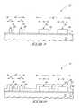
FIGS. 1-4 . Referring toFIG. 1 , a substrate, which may be a semiconductor substrate, is indicated generally withreference numeral 10. In the context of this document, the term “semiconductor substrate” or “semiconductive substrate” is defined to mean any construction comprising semiconductive material, including, but not limited to, bulk semiconductive materials such as a semiconductive wafer (either alone or in assemblies comprising other materials thereon), and semiconductive material layers (either alone or in assemblies comprising other materials). The term “substrate” refers to any supporting structure, including, but not limited to, the semiconductive substrates described above.Substrate 10 includes asemiconductive region 12 within which source/drain and channel regions (not shown) have or will be fabricated. Anexample material 12 is monocrystalline silicon suitably doped with one or more conductivity-enhancing impurities to one or more concentrations.Substrate 10 may include other layers or regions, for example trench isolation (not shown) which are not particularly material to the disclosure. - A gate dielectric14 has been formed over
substrate 12. An example thickness for gate dielectric14 is from about 3 nanometers to about 10 nanometers, with about 5 nanometers being a specific example. Afirst transistor gate 16 and asecond transistor gate 18 have been formed oversubstrate 12/14.First gate 16 has afirst width 17 andsecond gate 18 has asecond width 19, withfirst width 17 being narrower thansecond width 19. In the depicted embodiment, a plurality offirst gates 16 and a plurality ofsecond gates 18 have been formed oversubstrate 12/14, withfirst gates 16 having been formed within afirst area 20 andsecond gates 18 having been formed within a differentsecond area 22. Not all of the gates fabricated withinfirst area 20 are necessarily of the same material, size, or shape, and not all of the transistor gates fabricated withinsecond area 22 are necessarily of the same material, size, of shape. An examplefirst width 17 is from about 20 nanometers to about 75 nanometers, with about 50 nanometers being a specific example. Anexample width 19 is from about 40 nanometers to about 200 nanometers, with about 150 nanometers being a specific example. - In the context of this document, a “gate” or “transistor gate” alone refers to the conductive portion of a field-effect transistor gate construction, and a gate construction may include additional material, such as insulative sidewall spacers, an insulative cap, and/or a gate dielectric. The
example gates conductive region 24. However, insulative caps and/or spacers may be provided. Further, flash and other gate constructions might be used. Accordingly,conductive region 24 may comprise a control gate region or a floating gate region of a transistor.Conductive region 24 may be homogenous or non-homogenous. Example materials include conductively doped polysilicon, conductive metal compounds, and one or more elemental-form metals, including an alloy of multiple elemental-form metals. Example metals include platinum, cobalt, iridium, titanium, tungsten, tantalum, aluminum, iron, zirconium, vanadium, and hafnium. Transistor gates FIG. 1 depicting an etch ofmaterial 24 as having been conducted selectively relative togate dielectric 14 such that it remains spanning between adjacent of the conductive gates oversemiconductive material 12. Alternately, the processing might be conducted to not be selective, or etching continued to remove some or all of gate dielectric14 from being received oversubstrate material 12 between the gates. Further,FIG. 1 depicts an example wherein the transistor gates are fabricated to be of equal thickness, although multiple thicknesses and/or configurations may also be used. An example thickness forconductive region 24 is from about 10 nanometers to about 100 nanometers, with about 75 nanometers being a specific example. Additionally,FIG. 1 depicts the transistor orientation being planar or horizontal. Alternate configurations, such as vertical transistors and/or transistors formed in trenches, are also contemplated, and whether existing or yet-to-be developed.- Referring to
FIG. 2 , amaterial 28 has been deposited oversubstrate 10, including over first andsecond gates Material 28 may be insulative, conductive (including conductively doped semiconductive materials), or semiconductive, including any combination of such. Examples include silicon dioxide, silicon nitride, polysilicon, carbon, titanium nitride, tantalum nitride and tungsten nitride.Material 28 may be deposited to a thickness which is less than, equal to, or greater than each of first andsecond gates material 28 may be deposited substantially conformably or non-conformably over each of the first and second gates, and may be deposited to have a planar or non-planar outermost surface.FIG. 2 depicts an example whereinmaterial 28 has been deposited in a substantially conformal manner to have a non-planar outermost surface29, and to a thickness which is less than that of each of first andsecond gates material 28 is of different composition from that of an outermost portion ofconductive region 24 oftransistor gates - Referring to
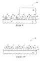
FIG. 3 ,substrate 10 has been placed within an etch chamber, andmaterial 28 has been etched from over both offirst gates 16 andsecond gates 18. The etching ofmaterial 28 has been effective to expose conductive material offirst gates 16 and to reduce thickness ofmaterial 28 received oversecond gates 18 yet to leavesecond gates 18 still covered bymaterial 28. By way of example only, example suitable etching chambers include high temperature plasma etchers which are capable of achieving substrate temperatures of at least 300° C., for example the etching chamber of the DPSII G3 HT plasma etching reactor sold by Applied Materials, Inc. of Santa Clara, Calif. and the etching chamber of the 2300 Kiyo plasma etching reactor sold by Lam Research Corporation of Fremont, Calif. Such ideally enable plasma etching which provide substrate temperature above 300° C., although other reactors might be used. - Such reactors may be operated in one embodiment to produce the example
FIG. 3 depicted result wherein the etching action has completely clearedmaterial 28 from being received over narrowerwidth transistor gates 16 as compared to widerwidth transistor gates 18, with the etching action ofFIG. 3 having been stopped at or shortly after exposure of narrowerwidth transistor gates 16. Suitable conditions and etching chemistries will be selected by the artisan depending upon the transistor gate width and the composition and configuration ofmaterial 28 received overtransistor gates narrow width gates 16 to help expose such features more quickly thanlarger width gates 18. For example, wherematerial 28 consists essentially of carbon, example conditions include substrate temperature from about 250° C. to about 400° C., chamber pressure from about 20 mTorr to about 100 mTorr, inductive power from about 100 W to about 500 W, and bias power from about 200 W to about 600 W. Example etch gases include from 0 sccm to about 500 sccm of one or a combination of Ar, He, Ne, Kr, and Xe, plus from about 50 sccm to about 200 sccm of N2, and from about 250 sccm to about 100 sccm of O2, with volumetric ratio of N2to O2ideally being at least 2:1. Alternate or overlapping conditions and chemistries can be determined by the artisan for materials other than carbon formaterial 28. The etching action may or may notclear material 28 from spanning between adjacent of the transistor gates, withFIG. 3 depicting an example wherein some thickness ofmaterial 28 remains spanning between adjacent transistor gates. - Referring to
FIG. 4 , and in situ within the etch chamber and after the etching ofFIG. 3 ,substrate 10 has been subjected to a plasma comprising a metal at a substrate temperature of at least 300° C. to diffuse said metal intofirst gates 16 to modify work function offirst gates 16 as compared to work function ofsecond gates 18. In the context of this document, in situ action requires the subjecting to be conducted in the very same chamber within which the etching occurred and without removing the substrate from the etch chamber between the etching and the subjecting to the plasma comprising the metal. The metal from the plasma may or may not be in a plasma state at the moment of starting the diffusion, and accordingly may alternately be in a gaseous state.FIG. 4 depicts the metal diffusion intoconductive regions 24 by stippling in the drawing, with the dots indicating the diffused metal. Such diffusion may or may not distribute the metal homogenously throughoutconductive region 24, and regardless of whetherconductive region 24 was homogenous before the exposure to the plasma containing the metal.FIG. 4 depicts an example wherein metal diffusion withinconductive region 24 of first gates26 is not homogenous throughoutregion 24. In such event, ideally diffusion of the metal from the plasma to withinconductive region 24 is to within at least about 10 nanometers of the depicted upper surface of gate dielectric14 to have a significant impact on work function of the gate. Further, the plasma to which the substrate is exposed may include one or more different metals such that one or more different metals might be diffused intoconductive region 24 offirst gates 16. Quantity of the metal diffused can be selected and determined by the artisan depending upon the impact desired on the work function of the gate. Further, such may be impacted based upon factors such as plasma composition, plasma conditions, time of exposure to the plasma, and composition of the conductive region into which the metal is diffusing. - Exposure to the plasma may or may not also diffuse the metal from the plasma into
material 28 received oversecond gates 18, and regardless material28 received oversecond gates 18 may or may not shield any of the metal from diffusing intosecond gates 18 during the exposure to plasma.FIG. 4 depicts an example wherein some diffusion of metal has also occurred intomaterial 28, but not having been effective to diffuse any metal to within any ofsecond gates 18.FIG. 5 depicts analternate embodiment substrate 10a, like numerals from the first-described embodiment have been utilized where appropriate, with differences being indicated with the suffix “a”. In the plasma exposure ofFIG. 5 , the diffusion of the metal has been effective to diffuse into and throughmaterial 28 into an outermost portion ofconductive region 24 ofsecond gates 18. Regardless, any such diffusion of metal to withinsecond gates 18 is considerably less than that intofirst gate 16 such that work function of the first gates is modified as compared to any work function modification which may or may not occur tosecond gates 18. - Diffusion of example metals that will inherently increase work function include platinum, cobalt and iridium where, for example,
conductive region 24 offirst gate 16 includes elemental-form metals or an alloy of elemental-form metals. Further, ifconductive region 24 prior to the metal diffusion includes an alloy including one or a combination of platinum, cobalt and iridium, diffusion of more platinum, cobalt and iridium into such conductive regions will tend to increase work function. Correspondingly, examples of metals which reduce work function in metal conductive regions include titanium, tungsten, tantalum, aluminum and iron. Further, for example if the outermost portion ofconductive region 24 comprises conductively doped polysilicon, diffusing of the metal may form the outermost portion ofconductive region 24 to comprise a conductive metal silicide. In one ideal embodiment, the metal in the plasma is derived from an organometallic compound. Examples include tetracarbonyl nickel for nickel, ferrocene for iron, Ti(N(CH3)2)4and/or Ti(N(C2H5)2)4for titanium, pentrkis-dimethyl amido-tantalum for tantalum, Co2(CO)8for cobalt, and Pt(C2H5C5H4)(CH3)3for platinum. Compounds other than organometallic might alternately be used, for example metal halides such as TiCl4and others. Example conditions in an inductively coupled high temperature etching reactor include substrate temperature from 300° C. to about 400° C., chamber pressure from about 5 mTorr to about 200 mTorr, inductive/source power from about 100 W to about 1,000 W, and bias power from 0 W to about 100 W. Example flow rates for the metal-containing gas are from about 10 sccm to about 200 sccm, and from 0 sccm to about 1,000 sccm of a suitable inert carrier gas to perhaps improve plasma uniformity and density (i.e., Ar, He, Xe, Kr, Ne and/or N2). Substrate temperature may be controlled by temperature of the susceptor or other support upon which the substrate rests. For example, the above described reactors may have their susceptors set to temperatures of 300° C. or higher, with the substrate temperature during the exposure to plasma being from about 10° C. to 50° C. higher depending on conditions of the plasma. - The etching of
FIG. 3 and the exposure to plasma ofFIG. 4 or5 may occur with or without any mask being received over any ofmaterial 28, with no mask being shown/received over any ofmaterial 28 in the depicted cross-section ofFIGS. 3-5 . - Another example embodiment method of forming a plurality of transistor gates having at least two different work functions is described with reference to
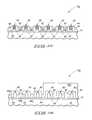
FIGS. 6-10 with respect to asubstrate 10b. Like numerals from the first-described embodiments have been utilized where appropriate, with differences being indicated with the suffix “b” or with different numerals. Referring toFIG. 6 , a plurality oftransistor gates 32 comprising aconductive region 33 have been formed over asubstrate 12/14. The transistor gates may or may not have at least two different widths, withgates 32 shown as having equal widths inFIG. 6 . The transistor gates ofFIG. 6 could have the example configurations of one or the other ofgates FIG. 1 , or other configurations. Composition ofconductive region 33, by way of example only, may be the same as that described above in connection withtransistors transistor gates 32. - A
material 34 has been provided overconductive region 33 oftransistor gates 32, with such material being of different composition from that of an outermost portion ofconductive region 33. Otherwise, example materials and attributes include any of those described above with respect tomaterial 28 in the first-described embodiment. - Referring to
FIG. 7 , amask 36 has been formed to cover some oftransistor gates 32 and leave others oftransistor gates 32 not covered bymask 36. Any suitable existing or yet-to-be developed mask might be utilized, and for example with such being either wholly or partly sacrificial. An example material includes photoresist with or without one or more anti-reflective coating layers. - Referring to
FIG. 8 , within a suitable etching chamber and after formingmask 36,material 34 has been etched from being received over thosetransistor gates 32 which are not covered bymask 36. Example chambers, chemistries and conditions include any of those described above in connection with the processing to produce theFIG. 3 substrate.Material 34 may or may not be etched to less than completely span between adjacent of the exposedtransistor gates 32 which are not covered bymask 36.FIG. 8 shows somematerial 34 spanning between adjacent of the exposedgates 32 after the etch. Alternately, all ofmaterial 34 not covered bymask 36 could be removed. - Referring to
FIG. 9 and in situ within the etch chamber after the etching ofFIG. 8 ,substrate 10bhas been subjected to a plasma comprising a metal at a substrate temperature of at least 300° C. The exposure to plasma has been effective to diffuse the metal from the plasma into the conductive region of thetransistor gates 32 which are not covered bymask 36 to modify work function of the uncoveredtransistor gates 32 as compared to work function oftransistor gates 32 which are covered bymask 36. Ideally,mask 36 shields any of the metal from the plasma from diffusing intoconductive region 33 of the covered/maskedtransistor gates 32. Example processing condition and chemistries are as described above in connection with theFIGS. 4 and 5 embodiments. Accordingly,conductive region 33 may or may not be homogenous before and after the exposure to plasma, and the metal may diffuse uniformly or only partially intoconductive region 33 to still have an impact upon and modify work function oftransistor gates 32 which are not covered bymask 36. - Embodiments of methods of forming a plurality of transistor gates may or may not result in at least two different work functions for different gates. The example embodiments as described above resulted in at least two different work functions for different gates. One example of an embodiment not necessarily resulting in at least two different work functions is shown with respect to a
substrate 10cinFIGS. 10-15 . Like numerals from the first-described embodiment have been utilized where appropriate, with differences being indicated with the suffix “c” or with different numerals. Referring toFIG. 10 , a plurality oftransistor gates 40 havingconductive regions 42 has been formed oversubstrate 12/14. Example materials and constructions include any of those described above with respect to theFIGS. 1-9 embodiments. Afirst material 44 has been deposited oversubstrate 12/14 including over and spanning between adjacent oftransistor gates 40.First material 44 is of different composition from that of an outermost portion ofconductive region 42 oftransistor gates 40. Example materials and attributes include any of those described above with respect tomaterials 28/34. Accordingly by way of example,first material 44 may or may not have a planar outermost surface, with a non-planar outermost surface being shown inFIG. 10 . - Referring to
FIG. 11 ,first material 44 has been etched to remove it from spanning between adjacent oftransistor gates 40 yet leavefirst material 44 covering tops and sidewalls oftransistor gates 40. - Referring to
FIG. 12 , asecond material 46 has been deposited over the substrate including over and spanning between adjacent oftransistor gates 40.Second material 46 may be the same or different in composition from that of an outermost portion offirst material 44. Further,second material 46 may have a planar or non-planar outermost surface, with a planar outermost surface being shown inFIG. 12 . Examples include any of those described above formaterial 28.Second material 46 may be deposited to a thickness which is less than, equal to, or greater than thickness oftransistor gates 40. - Referring to
FIG. 13 ,second material 46 has been etched from being received over at least some oftransistor gates 40 but remain spanning between adjacent oftransistor gates 40.FIG. 13 depicts an embodiment whereinsecond material 46 has been etched from being received over all oftransistor gates 40. Such might be conducted with or without masking. - Referring to
FIG. 14 , within an etch chamber and after etchingsecond material 46,first material 44 has been etched from being received over at least some oftransistor gates 40, withFIG. 14 depicting an example whereinfirst material 44 has been etched from being received over all oftransistor gates 40. Such etching may or may not be conducted selectively relative tosecond material 46 where such is of different composition fromfirst material 44, with a selective etching having been conducted as shown inFIG. 14 . Regardless, in one embodiment, etching ofsecond material 46 as shown inFIG. 13 may be conducted within the same etch chamber as the etching depicted byFIG. 14 . Further, in one embodiment, the etching offirst material 44 from being received over at least some oftransistor gates 40 as shown inFIG. 14 may occur in situ after the second material etch ofFIG. 13 . Example etching offirst material 44 inFIG. 14 may be conducted, for example, as described above in connection with any of theFIGS. 3 and 8 embodiments. - Referring to
FIG. 15 ,substrate 10chas been subjected to a plasma comprising a metal at a substrate temperature of at least 300° C. to diffuse the metal from the plasma intoconductive region 42 oftransistor gates 40 to modify work function oftransistor gates 40. Such subjecting/exposing has been conducted in situ within the etch chamber after the etching offirst material 44 from being received over at least some oftransistor gates 40 as was depicted inFIG. 14 . Example processing may be as described above with respect to any of theFIGS. 4 ,5 and9 embodiments. Where all transistor gates are exposed during the exposure to plasma as depicted byFIGS. 14 and 15 , work function of alltransistor gates 40 will be modified.FIGS. 16-18 depict an example alternate embodiment wherein at least two different work functions result, in part as a result of some of the second material remaining over some of the transistor gates during the exposure to plasma. - Specifically,
FIGS. 16-18 depict processing relative to analternate embodiment substrate 10d. Like numerals from the above-described embodiments have been utilized where appropriate, with differences being indicated with the suffix “d” or with different numerals.FIG. 16 depicts processing ofsubstrate 10dwith respect tosecond material 46dsubsequent to theFIG. 12 embodiment. InFIG. 16 ,second material 46dhas been masked (no mask being shown) while some ofsecond material 46dhas been left outwardly exposed and etched from being received elevationally over only some of transistor gates40 (specifically, the left three illustrated gates inFIG. 16 ). FIG. 17 depicts subsequent processing wherebyfirst material 44 has been etched from being received over the exposed, and thereby over only some of,transistor gates 40.FIG. 18 depicts subsequent processing wherein in situ within the etch chamber within which theFIG. 17 etching occurred,substrate 10dhas been exposed to the above-described metal-containing plasma to diffuse the metal intoconductive region 42 of the three leftillustrated transistor gates 40.- In one embodiment, a method encompasses forming a plurality of transistor gates comprising a conductive region over a substrate. The transistor gates may or may not have at least two different widths. Any of the above-described and shown plurality of transistor gates of
FIG. 1 ,6 or16 are examples of such transistor gates. A material is provided over the conductive region of the transistor gates, with such material being of different composition from that of an outermost portion of the conductive region of the transistor gates. Any one or a combination ofmaterial first material 44 andsecond material 46 in combination, regardless of whetherfirst material 44 is removed to not span completely betweentransistor gates 40, is also such an example material. Accordingly, “material” as used here and elsewhere in this document does not require homogeneity and may include multiple different composition and/or density regions and/or layers. - Within an etch chamber, the material is blanketly etched from being received over the conductive region of the transistor gates. Example chambers, chemistries, and conditions are as described above with the etching of any of
materials FIG. 13 toFIG. 14 may be considered as depicting such an embodiment wherebymaterial 44 is shown as being as blanketly etched from being received overconductive region 42 ofgates 40. Alternately by way of example only, the substrates ofFIGS. 2 and 6 might be blanketly etched to removematerial - Then, in situ within the etch chamber after the blanket etching, the substrate is subjected to a plasma comprising a metal at a substrate temperature of at least 300° C. to diffuse the metal from the plasma into the conductive region of the transistor gates to modify work function of the transistor gates. Example techniques, conditions, and chemistries for doing the same may be as those described above with respect to the processing of any of
FIGS. 4 ,5,9,15 and18. - In compliance with the statute, the subject matter disclosed herein has been described in language more or less specific as to structural and methodical features. It is to be understood, however, that the claims are not limited to the specific features shown and described, since the means herein disclosed comprise example embodiments. The claims are thus to be afforded full scope as literally worded, and to be appropriately interpreted in accordance with the doctrine of equivalents.
Claims (32)
Priority Applications (1)
| Application Number | Priority Date | Filing Date | Title |
|---|---|---|---|
| US13/248,625US8524561B2 (en) | 2008-11-05 | 2011-09-29 | Methods of forming a plurality of transistor gates, and methods of forming a plurality of transistor gates having at least two different work functions |
Applications Claiming Priority (3)
| Application Number | Priority Date | Filing Date | Title |
|---|---|---|---|
| US12/265,070US7824986B2 (en) | 2008-11-05 | 2008-11-05 | Methods of forming a plurality of transistor gates, and methods of forming a plurality of transistor gates having at least two different work functions |
| US12/904,038US8034687B2 (en) | 2008-11-05 | 2010-10-13 | Methods of forming a plurality of transistor gates, and methods of forming a plurality of transistor gates having at least two different work functions |
| US13/248,625US8524561B2 (en) | 2008-11-05 | 2011-09-29 | Methods of forming a plurality of transistor gates, and methods of forming a plurality of transistor gates having at least two different work functions |
Related Parent Applications (1)
| Application Number | Title | Priority Date | Filing Date |
|---|---|---|---|
| US12/904,038ContinuationUS8034687B2 (en) | 2008-11-05 | 2010-10-13 | Methods of forming a plurality of transistor gates, and methods of forming a plurality of transistor gates having at least two different work functions |
Publications (2)
| Publication Number | Publication Date |
|---|---|
| US20120021594A1true US20120021594A1 (en) | 2012-01-26 |
| US8524561B2 US8524561B2 (en) | 2013-09-03 |
Family
ID=42131944
Family Applications (3)
| Application Number | Title | Priority Date | Filing Date |
|---|---|---|---|
| US12/265,070Active2029-02-24US7824986B2 (en) | 2008-11-05 | 2008-11-05 | Methods of forming a plurality of transistor gates, and methods of forming a plurality of transistor gates having at least two different work functions |
| US12/904,038ActiveUS8034687B2 (en) | 2008-11-05 | 2010-10-13 | Methods of forming a plurality of transistor gates, and methods of forming a plurality of transistor gates having at least two different work functions |
| US13/248,625ActiveUS8524561B2 (en) | 2008-11-05 | 2011-09-29 | Methods of forming a plurality of transistor gates, and methods of forming a plurality of transistor gates having at least two different work functions |
Family Applications Before (2)
| Application Number | Title | Priority Date | Filing Date |
|---|---|---|---|
| US12/265,070Active2029-02-24US7824986B2 (en) | 2008-11-05 | 2008-11-05 | Methods of forming a plurality of transistor gates, and methods of forming a plurality of transistor gates having at least two different work functions |
| US12/904,038ActiveUS8034687B2 (en) | 2008-11-05 | 2010-10-13 | Methods of forming a plurality of transistor gates, and methods of forming a plurality of transistor gates having at least two different work functions |
Country Status (8)
| Country | Link |
|---|---|
| US (3) | US7824986B2 (en) |
| EP (1) | EP2342740B1 (en) |
| JP (1) | JP5333977B2 (en) |
| KR (1) | KR101173799B1 (en) |
| CN (1) | CN102203923B (en) |
| SG (2) | SG177975A1 (en) |
| TW (1) | TWI397975B (en) |
| WO (1) | WO2010053720A2 (en) |
Cited By (55)
| Publication number | Priority date | Publication date | Assignee | Title |
|---|---|---|---|---|
| US20110074498A1 (en)* | 2009-09-30 | 2011-03-31 | Suvolta, Inc. | Electronic Devices and Systems, and Methods for Making and Using the Same |
| US20110079861A1 (en)* | 2009-09-30 | 2011-04-07 | Lucian Shifren | Advanced Transistors with Threshold Voltage Set Dopant Structures |
| US20110121404A1 (en)* | 2009-09-30 | 2011-05-26 | Lucian Shifren | Advanced transistors with punch through suppression |
| US8377783B2 (en) | 2010-09-30 | 2013-02-19 | Suvolta, Inc. | Method for reducing punch-through in a transistor device |
| US8400219B2 (en) | 2011-03-24 | 2013-03-19 | Suvolta, Inc. | Analog circuits having improved transistors, and methods therefor |
| US8404551B2 (en) | 2010-12-03 | 2013-03-26 | Suvolta, Inc. | Source/drain extension control for advanced transistors |
| US8461875B1 (en) | 2011-02-18 | 2013-06-11 | Suvolta, Inc. | Digital circuits having improved transistors, and methods therefor |
| US20130217217A1 (en)* | 2012-02-22 | 2013-08-22 | Katsutoshi Kobayashi | Pattern forming method, semiconductor device manufacturing method, and coating apparatus |
| US8525271B2 (en) | 2011-03-03 | 2013-09-03 | Suvolta, Inc. | Semiconductor structure with improved channel stack and method for fabrication thereof |
| US8530286B2 (en) | 2010-04-12 | 2013-09-10 | Suvolta, Inc. | Low power semiconductor transistor structure and method of fabrication thereof |
| US8569156B1 (en) | 2011-05-16 | 2013-10-29 | Suvolta, Inc. | Reducing or eliminating pre-amorphization in transistor manufacture |
| US8569128B2 (en) | 2010-06-21 | 2013-10-29 | Suvolta, Inc. | Semiconductor structure and method of fabrication thereof with mixed metal types |
| US8599623B1 (en) | 2011-12-23 | 2013-12-03 | Suvolta, Inc. | Circuits and methods for measuring circuit elements in an integrated circuit device |
| US8614128B1 (en) | 2011-08-23 | 2013-12-24 | Suvolta, Inc. | CMOS structures and processes based on selective thinning |
| US8629016B1 (en) | 2011-07-26 | 2014-01-14 | Suvolta, Inc. | Multiple transistor types formed in a common epitaxial layer by differential out-diffusion from a doped underlayer |
| US8637955B1 (en) | 2012-08-31 | 2014-01-28 | Suvolta, Inc. | Semiconductor structure with reduced junction leakage and method of fabrication thereof |
| US8645878B1 (en) | 2011-08-23 | 2014-02-04 | Suvolta, Inc. | Porting a circuit design from a first semiconductor process to a second semiconductor process |
| US8713511B1 (en) | 2011-09-16 | 2014-04-29 | Suvolta, Inc. | Tools and methods for yield-aware semiconductor manufacturing process target generation |
| US8735987B1 (en) | 2011-06-06 | 2014-05-27 | Suvolta, Inc. | CMOS gate stack structures and processes |
| US8748986B1 (en) | 2011-08-05 | 2014-06-10 | Suvolta, Inc. | Electronic device with controlled threshold voltage |
| US8748270B1 (en) | 2011-03-30 | 2014-06-10 | Suvolta, Inc. | Process for manufacturing an improved analog transistor |
| US8759872B2 (en) | 2010-06-22 | 2014-06-24 | Suvolta, Inc. | Transistor with threshold voltage set notch and method of fabrication thereof |
| US8796048B1 (en) | 2011-05-11 | 2014-08-05 | Suvolta, Inc. | Monitoring and measurement of thin film layers |
| US8811068B1 (en) | 2011-05-13 | 2014-08-19 | Suvolta, Inc. | Integrated circuit devices and methods |
| US8819603B1 (en) | 2011-12-15 | 2014-08-26 | Suvolta, Inc. | Memory circuits and methods of making and designing the same |
| US8816754B1 (en) | 2012-11-02 | 2014-08-26 | Suvolta, Inc. | Body bias circuits and methods |
| US8863064B1 (en) | 2012-03-23 | 2014-10-14 | Suvolta, Inc. | SRAM cell layout structure and devices therefrom |
| US8877619B1 (en) | 2012-01-23 | 2014-11-04 | Suvolta, Inc. | Process for manufacture of integrated circuits with different channel doping transistor architectures and devices therefrom |
| US8883600B1 (en) | 2011-12-22 | 2014-11-11 | Suvolta, Inc. | Transistor having reduced junction leakage and methods of forming thereof |
| US8895327B1 (en) | 2011-12-09 | 2014-11-25 | Suvolta, Inc. | Tipless transistors, short-tip transistors, and methods and circuits therefor |
| US8970289B1 (en) | 2012-01-23 | 2015-03-03 | Suvolta, Inc. | Circuits and devices for generating bi-directional body bias voltages, and methods therefor |
| US8976575B1 (en) | 2013-08-29 | 2015-03-10 | Suvolta, Inc. | SRAM performance monitor |
| US8988153B1 (en) | 2013-03-09 | 2015-03-24 | Suvolta, Inc. | Ring oscillator with NMOS or PMOS variation insensitivity |
| US8995204B2 (en) | 2011-06-23 | 2015-03-31 | Suvolta, Inc. | Circuit devices and methods having adjustable transistor body bias |
| US8994415B1 (en) | 2013-03-01 | 2015-03-31 | Suvolta, Inc. | Multiple VDD clock buffer |
| US8999861B1 (en) | 2011-05-11 | 2015-04-07 | Suvolta, Inc. | Semiconductor structure with substitutional boron and method for fabrication thereof |
| US9041126B2 (en) | 2012-09-21 | 2015-05-26 | Mie Fujitsu Semiconductor Limited | Deeply depleted MOS transistors having a screening layer and methods thereof |
| US9054219B1 (en) | 2011-08-05 | 2015-06-09 | Mie Fujitsu Semiconductor Limited | Semiconductor devices having fin structures and fabrication methods thereof |
| US9070477B1 (en) | 2012-12-12 | 2015-06-30 | Mie Fujitsu Semiconductor Limited | Bit interleaved low voltage static random access memory (SRAM) and related methods |
| US9093550B1 (en) | 2012-01-31 | 2015-07-28 | Mie Fujitsu Semiconductor Limited | Integrated circuits having a plurality of high-K metal gate FETs with various combinations of channel foundation structure and gate stack structure and methods of making same |
| US9093997B1 (en) | 2012-11-15 | 2015-07-28 | Mie Fujitsu Semiconductor Limited | Slew based process and bias monitors and related methods |
| US9112057B1 (en) | 2012-09-18 | 2015-08-18 | Mie Fujitsu Semiconductor Limited | Semiconductor devices with dopant migration suppression and method of fabrication thereof |
| US9112484B1 (en) | 2012-12-20 | 2015-08-18 | Mie Fujitsu Semiconductor Limited | Integrated circuit process and bias monitors and related methods |
| US9112495B1 (en) | 2013-03-15 | 2015-08-18 | Mie Fujitsu Semiconductor Limited | Integrated circuit device body bias circuits and methods |
| US20150340451A1 (en)* | 2014-05-26 | 2015-11-26 | Semiconductor Manufacturing International (Shanghai) Corporation | Method for cmp of high-k metal gate structures |
| US9236466B1 (en) | 2011-10-07 | 2016-01-12 | Mie Fujitsu Semiconductor Limited | Analog circuits having improved insulated gate transistors, and methods therefor |
| US9268885B1 (en) | 2013-02-28 | 2016-02-23 | Mie Fujitsu Semiconductor Limited | Integrated circuit device methods and models with predicted device metric variations |
| US9299801B1 (en) | 2013-03-14 | 2016-03-29 | Mie Fujitsu Semiconductor Limited | Method for fabricating a transistor device with a tuned dopant profile |
| US9299698B2 (en) | 2012-06-27 | 2016-03-29 | Mie Fujitsu Semiconductor Limited | Semiconductor structure with multiple transistors having various threshold voltages |
| US9319013B2 (en) | 2014-08-19 | 2016-04-19 | Mie Fujitsu Semiconductor Limited | Operational amplifier input offset correction with transistor threshold voltage adjustment |
| US9406567B1 (en) | 2012-02-28 | 2016-08-02 | Mie Fujitsu Semiconductor Limited | Method for fabricating multiple transistor devices on a substrate with varying threshold voltages |
| US9431068B2 (en) | 2012-10-31 | 2016-08-30 | Mie Fujitsu Semiconductor Limited | Dynamic random access memory (DRAM) with low variation transistor peripheral circuits |
| US9449967B1 (en) | 2013-03-15 | 2016-09-20 | Fujitsu Semiconductor Limited | Transistor array structure |
| US9478571B1 (en) | 2013-05-24 | 2016-10-25 | Mie Fujitsu Semiconductor Limited | Buried channel deeply depleted channel transistor |
| US9710006B2 (en) | 2014-07-25 | 2017-07-18 | Mie Fujitsu Semiconductor Limited | Power up body bias circuits and methods |
Families Citing this family (24)
| Publication number | Priority date | Publication date | Assignee | Title |
|---|---|---|---|---|
| US8008144B2 (en) | 2006-05-11 | 2011-08-30 | Micron Technology, Inc. | Dual work function recessed access device and methods of forming |
| US8860174B2 (en)* | 2006-05-11 | 2014-10-14 | Micron Technology, Inc. | Recessed antifuse structures and methods of making the same |
| US20070262395A1 (en) | 2006-05-11 | 2007-11-15 | Gibbons Jasper S | Memory cell access devices and methods of making the same |
| US7824986B2 (en)* | 2008-11-05 | 2010-11-02 | Micron Technology, Inc. | Methods of forming a plurality of transistor gates, and methods of forming a plurality of transistor gates having at least two different work functions |
| IT1401141B1 (en)* | 2010-07-26 | 2013-07-12 | Indena Spa | FORMULATIONS CONTAINING EXTRACTS OF ECHINACEA ANGUSTIFOLIA AND ZINGIBER OFFICINALE USEFUL IN THE REDUCTION OF INFLAMMATION AND PERIPHERAL PAIN |
| US9412883B2 (en) | 2011-11-22 | 2016-08-09 | Taiwan Semiconductor Manufacturing Company, Ltd. | Methods and apparatus for MOS capacitors in replacement gate process |
| US9269833B2 (en) | 2011-11-22 | 2016-02-23 | Taiwan Semiconductor Manufacturing Company, Ltd. | Methods and apparatus for hybrid MOS capacitors in replacement gate process |
| US8896035B2 (en) | 2012-10-22 | 2014-11-25 | International Business Machines Corporation | Field effect transistor having phase transition material incorporated into one or more components for reduced leakage current |
| KR102055379B1 (en) | 2013-08-08 | 2019-12-13 | 삼성전자 주식회사 | Semiconductor device having tri-gate and manufacturing method thereof |
| CN104779205B (en)* | 2014-01-15 | 2018-06-26 | 南方科技大学 | Method for adjusting work function by integrating metal layers with different thicknesses |
| WO2017213640A1 (en)* | 2016-06-08 | 2017-12-14 | Intel Corporation | Quantum dot devices |
| WO2017213638A1 (en)* | 2016-06-08 | 2017-12-14 | Intel Corporation | Quantum dot devices with doped regions |
| US11158714B2 (en) | 2016-06-09 | 2021-10-26 | Intel Corporation | Quantum dot devices with trenched substrates |
| WO2017213648A1 (en)* | 2016-06-09 | 2017-12-14 | Intel Corporation | Quantum dot devices with doped conductive pathways |
| WO2017213649A1 (en)* | 2016-06-09 | 2017-12-14 | Intel Corporation | Quantum dot devices with double quantum well structures |
| WO2017213658A1 (en)* | 2016-06-10 | 2017-12-14 | Intel Corporation | Gate patterning for quantum dot devices |
| WO2018031006A1 (en) | 2016-08-10 | 2018-02-15 | Intel Corporation | Quantum dot array devices |
| EP3497725A4 (en) | 2016-08-10 | 2020-04-15 | Intel Corporation | QUANTUM POINT ARRAY DEVICE |
| WO2018031027A1 (en)* | 2016-08-12 | 2018-02-15 | Intel Corporation | Quantum dot array devices |
| WO2018044267A1 (en)* | 2016-08-30 | 2018-03-08 | Intel Corporation | Quantum dot devices |
| CN109643726A (en) | 2016-08-30 | 2019-04-16 | 英特尔公司 | Quantum dot device |
| US9997519B1 (en) | 2017-05-03 | 2018-06-12 | International Business Machines Corporation | Dual channel structures with multiple threshold voltages |
| US10037919B1 (en) | 2017-05-31 | 2018-07-31 | Globalfoundries Inc. | Integrated single-gated vertical field effect transistor (VFET) and independent double-gated VFET |
| US11616126B2 (en) | 2018-09-27 | 2023-03-28 | Intel Corporation | Quantum dot devices with passive barrier elements in a quantum well stack between metal gates |
Citations (2)
| Publication number | Priority date | Publication date | Assignee | Title |
|---|---|---|---|---|
| US20090230463A1 (en)* | 2008-03-14 | 2009-09-17 | Advanced Micro Devices, Inc. | Integrated circuit long and short channel metal gate devices and method of manufacture |
| US7824986B2 (en)* | 2008-11-05 | 2010-11-02 | Micron Technology, Inc. | Methods of forming a plurality of transistor gates, and methods of forming a plurality of transistor gates having at least two different work functions |
Family Cites Families (109)
| Publication number | Priority date | Publication date | Assignee | Title |
|---|---|---|---|---|
| US714858A (en)* | 1902-04-18 | 1902-12-02 | William R Brixey | Manufacture of crude kerite. |
| US4636834A (en) | 1983-12-12 | 1987-01-13 | International Business Machines Corporation | Submicron FET structure and method of making |
| US4714519A (en) | 1987-03-30 | 1987-12-22 | Motorola, Inc. | Method for fabricating MOS transistors having gates with different work functions |
| US5013680A (en) | 1990-07-18 | 1991-05-07 | Micron Technology, Inc. | Process for fabricating a DRAM array having feature widths that transcend the resolution limit of available photolithography |
| US5122848A (en) | 1991-04-08 | 1992-06-16 | Micron Technology, Inc. | Insulated-gate vertical field-effect transistor with high current drive and minimum overlap capacitance |
| JP3215898B2 (en)* | 1992-04-28 | 2001-10-09 | 日本電信電話株式会社 | Plasma CVD method and plasma CVD apparatus |
| KR100362751B1 (en) | 1994-01-19 | 2003-02-11 | 소니 가부시끼 가이샤 | Contact hole and method for forming the semiconductor device |
| US5583065A (en) | 1994-11-23 | 1996-12-10 | Sony Corporation | Method of making a MOS semiconductor device |
| US5547890A (en) | 1995-05-05 | 1996-08-20 | Vanguard International Semiconductor Corporation | DRAM cell with a cradle-type capacitor |
| KR100202633B1 (en)* | 1995-07-26 | 1999-06-15 | 구본준 | Semiconductor device manufacturing method |
| US5714412A (en) | 1996-12-02 | 1998-02-03 | Taiwan Semiconductor Manufacturing Company, Ltd | Multi-level, split-gate, flash memory cell and method of manufacture thereof |
| TW377496B (en) | 1997-01-15 | 1999-12-21 | United Microelectronics Corp | Method of manufacturing read-only memory structure |
| US6191470B1 (en) | 1997-07-08 | 2001-02-20 | Micron Technology, Inc. | Semiconductor-on-insulator memory cell with buried word and body lines |
| US6072209A (en) | 1997-07-08 | 2000-06-06 | Micro Technology, Inc. | Four F2 folded bit line DRAM cell structure having buried bit and word lines |
| US6150687A (en) | 1997-07-08 | 2000-11-21 | Micron Technology, Inc. | Memory cell having a vertical transistor with buried source/drain and dual gates |
| US5909618A (en) | 1997-07-08 | 1999-06-01 | Micron Technology, Inc. | Method of making memory cell with vertical transistor and buried word and body lines |
| US5960270A (en) | 1997-08-11 | 1999-09-28 | Motorola, Inc. | Method for forming an MOS transistor having a metallic gate electrode that is formed after the formation of self-aligned source and drain regions |
| US6333556B1 (en)* | 1997-10-09 | 2001-12-25 | Micron Technology, Inc. | Insulating materials |
| US5953614A (en) | 1997-10-09 | 1999-09-14 | Lsi Logic Corporation | Process for forming self-aligned metal silicide contacts for MOS structure using single silicide-forming step |
| US6121100A (en) | 1997-12-31 | 2000-09-19 | Intel Corporation | Method of fabricating a MOS transistor with a raised source/drain extension |
| US6187619B1 (en)* | 1998-02-17 | 2001-02-13 | Shye-Lin Wu | Method to fabricate short-channel MOSFETs with an improvement in ESD resistance |
| US5963469A (en) | 1998-02-24 | 1999-10-05 | Micron Technology, Inc. | Vertical bipolar read access for low voltage memory cell |
| US6259142B1 (en) | 1998-04-07 | 2001-07-10 | Advanced Micro Devices, Inc. | Multiple split gate semiconductor device and fabrication method |
| US6696746B1 (en) | 1998-04-29 | 2004-02-24 | Micron Technology, Inc. | Buried conductors |
| US6027961A (en)* | 1998-06-30 | 2000-02-22 | Motorola, Inc. | CMOS semiconductor devices and method of formation |
| US5941701A (en) | 1998-07-14 | 1999-08-24 | Ceramoptec Ind Inc | Device and method to treat oral disease in felines |
| KR100304717B1 (en) | 1998-08-18 | 2001-11-15 | 김덕중 | Semiconductor device having a trench type gate and method for fabricating therefor |
| US6204103B1 (en)* | 1998-09-18 | 2001-03-20 | Intel Corporation | Process to make complementary silicide metal gates for CMOS technology |
| US6225669B1 (en) | 1998-09-30 | 2001-05-01 | Advanced Micro Devices, Inc. | Non-uniform gate/dielectric field effect transistor |
| US6373114B1 (en) | 1998-10-23 | 2002-04-16 | Micron Technology, Inc. | Barrier in gate stack for improved gate dielectric integrity |
| US5977579A (en) | 1998-12-03 | 1999-11-02 | Micron Technology, Inc. | Trench dram cell with vertical device and buried word lines |
| US6130453A (en) | 1999-01-04 | 2000-10-10 | International Business Machines Corporation | Flash memory structure with floating gate in vertical trench |
| US6291282B1 (en)* | 1999-02-26 | 2001-09-18 | Texas Instruments Incorporated | Method of forming dual metal gate structures or CMOS devices |
| KR100282452B1 (en) | 1999-03-18 | 2001-02-15 | 김영환 | Semiconductor device and method for fabricating the same |
| US6373111B1 (en) | 1999-11-30 | 2002-04-16 | Intel Corporation | Work function tuning for MOSFET gate electrodes |
| US6383879B1 (en) | 1999-12-03 | 2002-05-07 | Agere Systems Guardian Corp. | Semiconductor device having a metal gate with a work function compatible with a semiconductor device |
| US6956263B1 (en) | 1999-12-28 | 2005-10-18 | Intel Corporation | Field effect transistor structure with self-aligned raised source/drain extensions |
| US6343114B1 (en) | 1999-12-30 | 2002-01-29 | Turnstone Systems, Inc. | Remotely addressable maintenance unit |
| JP3851752B2 (en) | 2000-03-27 | 2006-11-29 | 株式会社東芝 | Manufacturing method of semiconductor device |
| KR100327434B1 (en) | 2000-05-01 | 2002-03-13 | 박종섭 | Semiconductor device |
| KR100821456B1 (en) | 2000-08-14 | 2008-04-11 | 샌디스크 쓰리디 엘엘씨 | Dense array and charge storage device and manufacturing method thereof |
| US6294434B1 (en)* | 2000-09-27 | 2001-09-25 | Vanguard International Semiconductor Corporation | Method of forming a metal silicide layer on a polysilicon gate structure and on a source/drain region of a MOSFET device |
| GB0028031D0 (en) | 2000-11-17 | 2001-01-03 | Koninkl Philips Electronics Nv | Trench-gate field-effect transistors and their manufacture |
| US6552401B1 (en) | 2000-11-27 | 2003-04-22 | Micron Technology | Use of gate electrode workfunction to improve DRAM refresh |
| US6300177B1 (en) | 2001-01-25 | 2001-10-09 | Chartered Semiconductor Manufacturing Inc. | Method to form transistors with multiple threshold voltages (VT) using a combination of different work function gate materials |
| US20020132473A1 (en) | 2001-03-13 | 2002-09-19 | Applied Materials ,Inc. | Integrated barrier layer structure for copper contact level metallization |
| JP4236848B2 (en) | 2001-03-28 | 2009-03-11 | セイコーインスツル株式会社 | Manufacturing method of semiconductor integrated circuit device |
| JP2002305254A (en)* | 2001-04-05 | 2002-10-18 | Mitsubishi Electric Corp | Semiconductor device and manufacturing method thereof |
| US6498062B2 (en) | 2001-04-27 | 2002-12-24 | Micron Technology, Inc. | DRAM access transistor |
| DK1425272T3 (en) | 2001-08-31 | 2011-11-21 | Novartis Ag | Optical isomers of an iloperidone metabolite |
| US6534402B1 (en)* | 2001-11-01 | 2003-03-18 | Winbond Electronics Corp. | Method of fabricating self-aligned silicide |
| US6610576B2 (en) | 2001-12-13 | 2003-08-26 | International Business Machines Corporation | Method for forming asymmetric dual gate transistor |
| US6653698B2 (en)* | 2001-12-20 | 2003-11-25 | International Business Machines Corporation | Integration of dual workfunction metal gate CMOS devices |
| US6630720B1 (en) | 2001-12-26 | 2003-10-07 | Advanced Micro Devices, Inc. | Asymmetric semiconductor device having dual work function gate and method of fabrication |
| US6794234B2 (en)* | 2002-01-30 | 2004-09-21 | The Regents Of The University Of California | Dual work function CMOS gate technology based on metal interdiffusion |
| US6562713B1 (en)* | 2002-02-19 | 2003-05-13 | International Business Machines Corporation | Method of protecting semiconductor areas while exposing a gate |
| KR100502407B1 (en) | 2002-04-11 | 2005-07-19 | 삼성전자주식회사 | Gate Structure Having High-k Dielectric And Highly Conductive Electrode And Method Of Forming The Same |
| US6806123B2 (en) | 2002-04-26 | 2004-10-19 | Micron Technology, Inc. | Methods of forming isolation regions associated with semiconductor constructions |
| US7071043B2 (en) | 2002-08-15 | 2006-07-04 | Micron Technology, Inc. | Methods of forming a field effect transistor having source/drain material over insulative material |
| US7045406B2 (en)* | 2002-12-03 | 2006-05-16 | Asm International, N.V. | Method of forming an electrode with adjusted work function |
| US7316950B2 (en)* | 2003-04-22 | 2008-01-08 | National University Of Singapore | Method of fabricating a CMOS device with dual metal gate electrodes |
| KR100505113B1 (en) | 2003-04-23 | 2005-07-29 | 삼성전자주식회사 | Mosfet and method of fabricating the same |
| WO2004107421A1 (en)* | 2003-06-03 | 2004-12-09 | Koninklijke Philips Electronics N.V. | Formation of junctions and silicides with reduced thermal budget |
| KR100511045B1 (en) | 2003-07-14 | 2005-08-30 | 삼성전자주식회사 | Integration method of a semiconductor device having a recessed gate electrode |
| KR100488546B1 (en)* | 2003-08-29 | 2005-05-11 | 삼성전자주식회사 | Method for manufacturing transistor |
| US7112483B2 (en)* | 2003-08-29 | 2006-09-26 | Taiwan Semiconductor Manufacturing Company, Ltd. | Method for forming a device having multiple silicide types |
| US6844591B1 (en) | 2003-09-17 | 2005-01-18 | Micron Technology, Inc. | Method of forming DRAM access transistors |
| US7029966B2 (en) | 2003-09-18 | 2006-04-18 | International Business Machines Corporation | Process options of forming silicided metal gates for advanced CMOS devices |
| US6963108B1 (en) | 2003-10-10 | 2005-11-08 | Advanced Micro Devices, Inc. | Recessed channel |
| JP4085051B2 (en) | 2003-12-26 | 2008-04-30 | 株式会社東芝 | Semiconductor device and manufacturing method thereof |
| US7148104B2 (en) | 2004-03-10 | 2006-12-12 | Promos Technologies Inc. | Fabrication of conductive lines interconnecting first conductive gates in nonvolatile memories having second conductive gates provided by conductive gate lines, wherein the adjacent conductive gate lines for the adjacent columns are spaced from each other, and non-volatile memory structures |
| US7262089B2 (en) | 2004-03-11 | 2007-08-28 | Micron Technology, Inc. | Methods of forming semiconductor structures |
| US7285829B2 (en) | 2004-03-31 | 2007-10-23 | Intel Corporation | Semiconductor device having a laterally modulated gate workfunction and method of fabrication |
| US7226826B2 (en)* | 2004-04-16 | 2007-06-05 | Texas Instruments Incorporated | Semiconductor device having multiple work functions and method of manufacture therefor |
| KR100614240B1 (en) | 2004-06-10 | 2006-08-18 | 삼성전자주식회사 | Semiconductor device including field effect transistor and method for forming same |
| JP2006013332A (en) | 2004-06-29 | 2006-01-12 | Sumitomo Electric Ind Ltd | Connector, manufacturing method and connection method thereof, and connected electronic device |
| KR100629263B1 (en) | 2004-07-23 | 2006-09-29 | 삼성전자주식회사 | Morse transistor having recessed gate electrode and manufacturing method thereof |
| US7122425B2 (en) | 2004-08-24 | 2006-10-17 | Micron Technology, Inc. | Methods of forming semiconductor constructions |
| US7795094B2 (en) | 2004-09-02 | 2010-09-14 | Micron Technology, Inc. | Recessed gate dielectric antifuse |
| US7285812B2 (en) | 2004-09-02 | 2007-10-23 | Micron Technology, Inc. | Vertical transistors |
| JP4116990B2 (en) | 2004-09-28 | 2008-07-09 | 富士通株式会社 | Field effect transistor and manufacturing method thereof |
| US7611943B2 (en) | 2004-10-20 | 2009-11-03 | Texas Instruments Incorporated | Transistors, integrated circuits, systems, and processes of manufacture with improved work function modulation |
| KR100699830B1 (en) | 2004-12-16 | 2007-03-27 | 삼성전자주식회사 | Non-volatile memory device and method for improving erase efficiency |
| KR100719340B1 (en) | 2005-01-14 | 2007-05-17 | 삼성전자주식회사 | Semiconductor device having a dual gate electrode and method of forming the same |
| KR100632953B1 (en) | 2005-03-07 | 2006-10-12 | 삼성전자주식회사 | A memory device, a memory array for the memory device, and a method of driving the memory array |
| US7244659B2 (en) | 2005-03-10 | 2007-07-17 | Micron Technology, Inc. | Integrated circuits and methods of forming a field effect transistor |
| US7384849B2 (en) | 2005-03-25 | 2008-06-10 | Micron Technology, Inc. | Methods of forming recessed access devices associated with semiconductor constructions |
| US7214621B2 (en) | 2005-05-18 | 2007-05-08 | Micron Technology, Inc. | Methods of forming devices associated with semiconductor constructions |
| JP4591827B2 (en) | 2005-05-24 | 2010-12-01 | エルピーダメモリ株式会社 | Semiconductor device including cell transistor having recess channel structure and manufacturing method thereof |
| US7282401B2 (en) | 2005-07-08 | 2007-10-16 | Micron Technology, Inc. | Method and apparatus for a self-aligned recessed access device (RAD) transistor gate |
| US7202535B2 (en) | 2005-07-14 | 2007-04-10 | Infineon Technologies Ag | Manufacturing method for an integrated semiconductor structure and corresponding integrated semiconductor structure |
| JP5114881B2 (en)* | 2005-07-26 | 2013-01-09 | 富士通セミコンダクター株式会社 | Semiconductor device and manufacturing method thereof |
| US7229873B2 (en)* | 2005-08-10 | 2007-06-12 | Texas Instruments Incorporated | Process for manufacturing dual work function metal gates in a microelectronics device |
| US7332433B2 (en)* | 2005-09-22 | 2008-02-19 | Sematech Inc. | Methods of modulating the work functions of film layers |
| KR100689840B1 (en) | 2005-10-04 | 2007-03-08 | 삼성전자주식회사 | Semiconductor device having recessed gate electrode and method of manufacturing same |
| EP1772898A1 (en)* | 2005-10-06 | 2007-04-11 | Interuniversitair Microelektronica Centrum ( Imec) | Method for forming a silicide gate |
| EP1801856A1 (en) | 2005-12-23 | 2007-06-27 | Interuniversitair Microelektronica Centrum ( Imec) | Method for gate electrode height control |
| US7349232B2 (en) | 2006-03-15 | 2008-03-25 | Micron Technology, Inc. | 6F2 DRAM cell design with 3F-pitch folded digitline sense amplifier |
| JP2007251030A (en) | 2006-03-17 | 2007-09-27 | Renesas Technology Corp | Semiconductor device manufacturing method and semiconductor device |
| US7902597B2 (en) | 2006-03-22 | 2011-03-08 | Samsung Electronics Co., Ltd. | Transistors with laterally extended active regions and methods of fabricating same |
| US20070262395A1 (en) | 2006-05-11 | 2007-11-15 | Gibbons Jasper S | Memory cell access devices and methods of making the same |
| US8860174B2 (en) | 2006-05-11 | 2014-10-14 | Micron Technology, Inc. | Recessed antifuse structures and methods of making the same |
| US8008144B2 (en) | 2006-05-11 | 2011-08-30 | Micron Technology, Inc. | Dual work function recessed access device and methods of forming |
| JP5280843B2 (en)* | 2006-05-25 | 2013-09-04 | ルネサスエレクトロニクス株式会社 | Method for forming metal compound layer and apparatus for forming metal compound layer |
| KR100770536B1 (en)* | 2006-07-19 | 2007-10-25 | 동부일렉트로닉스 주식회사 | High voltage semiconductor device and manufacturing method thereof |
| US7494878B2 (en)* | 2006-10-25 | 2009-02-24 | United Microelectronics Corp. | Metal-oxide-semiconductor transistor and method of forming the same |
| US20080146012A1 (en)* | 2006-12-15 | 2008-06-19 | Taiwan Semiconductor Manufacturing Company, Ltd. | Novel method to adjust work function by plasma assisted metal incorporated dielectric |
| US7629655B2 (en)* | 2007-03-20 | 2009-12-08 | Taiwan Semiconductor Manufacturing Company, Ltd. | Semiconductor device with multiple silicide regions |
| US7875919B2 (en) | 2008-03-31 | 2011-01-25 | International Business Machines Corporation | Shallow trench capacitor compatible with high-K / metal gate |
- 2008
- 2008-11-05USUS12/265,070patent/US7824986B2/enactiveActive
- 2009
- 2009-10-23WOPCT/US2009/061823patent/WO2010053720A2/enactiveApplication Filing
- 2009-10-23JPJP2011534644Apatent/JP5333977B2/enactiveActive
- 2009-10-23EPEP09825209.1Apatent/EP2342740B1/enactiveActive
- 2009-10-23SGSG2012002648Apatent/SG177975A1/enunknown
- 2009-10-23KRKR1020117010387Apatent/KR101173799B1/enactiveActive
- 2009-10-23SGSG2012002655Apatent/SG177976A1/enunknown
- 2009-10-23CNCN200980143451.8Apatent/CN102203923B/enactiveActive
- 2009-11-04TWTW098137445Apatent/TWI397975B/enactive
- 2010
- 2010-10-13USUS12/904,038patent/US8034687B2/enactiveActive
- 2011
- 2011-09-29USUS13/248,625patent/US8524561B2/enactiveActive
Patent Citations (3)
| Publication number | Priority date | Publication date | Assignee | Title |
|---|---|---|---|---|
| US20090230463A1 (en)* | 2008-03-14 | 2009-09-17 | Advanced Micro Devices, Inc. | Integrated circuit long and short channel metal gate devices and method of manufacture |
| US7824986B2 (en)* | 2008-11-05 | 2010-11-02 | Micron Technology, Inc. | Methods of forming a plurality of transistor gates, and methods of forming a plurality of transistor gates having at least two different work functions |
| US8034687B2 (en)* | 2008-11-05 | 2011-10-11 | Micron Technology, Inc. | Methods of forming a plurality of transistor gates, and methods of forming a plurality of transistor gates having at least two different work functions |
Cited By (125)
| Publication number | Priority date | Publication date | Assignee | Title |
|---|---|---|---|---|
| US20110074498A1 (en)* | 2009-09-30 | 2011-03-31 | Suvolta, Inc. | Electronic Devices and Systems, and Methods for Making and Using the Same |
| US9508800B2 (en) | 2009-09-30 | 2016-11-29 | Mie Fujitsu Semiconductor Limited | Advanced transistors with punch through suppression |
| US20110121404A1 (en)* | 2009-09-30 | 2011-05-26 | Lucian Shifren | Advanced transistors with punch through suppression |
| US8273617B2 (en) | 2009-09-30 | 2012-09-25 | Suvolta, Inc. | Electronic devices and systems, and methods for making and using the same |
| US8975128B2 (en) | 2009-09-30 | 2015-03-10 | Suvolta, Inc. | Electronic devices and systems, and methods for making and using the same |
| US9263523B2 (en) | 2009-09-30 | 2016-02-16 | Mie Fujitsu Semiconductor Limited | Advanced transistors with punch through suppression |
| US20110079861A1 (en)* | 2009-09-30 | 2011-04-07 | Lucian Shifren | Advanced Transistors with Threshold Voltage Set Dopant Structures |
| US8421162B2 (en) | 2009-09-30 | 2013-04-16 | Suvolta, Inc. | Advanced transistors with punch through suppression |
| US10074568B2 (en) | 2009-09-30 | 2018-09-11 | Mie Fujitsu Semiconductor Limited | Electronic devices and systems, and methods for making and using same |
| US11887895B2 (en) | 2009-09-30 | 2024-01-30 | United Semiconductor Japan Co., Ltd. | Electronic devices and systems, and methods for making and using the same |
| US10217668B2 (en) | 2009-09-30 | 2019-02-26 | Mie Fujitsu Semiconductor Limited | Electronic devices and systems, and methods for making and using the same |
| US10224244B2 (en) | 2009-09-30 | 2019-03-05 | Mie Fujitsu Semiconductor Limited | Electronic devices and systems, and methods for making and using the same |
| US8541824B2 (en) | 2009-09-30 | 2013-09-24 | Suvolta, Inc. | Electronic devices and systems, and methods for making and using the same |
| US8604530B2 (en) | 2009-09-30 | 2013-12-10 | Suvolta, Inc. | Electronic devices and systems, and methods for making and using the same |
| US11062950B2 (en) | 2009-09-30 | 2021-07-13 | United Semiconductor Japan Co., Ltd. | Electronic devices and systems, and methods for making and using the same |
| US8604527B2 (en) | 2009-09-30 | 2013-12-10 | Suvolta, Inc. | Electronic devices and systems, and methods for making and using the same |
| US10325986B2 (en) | 2009-09-30 | 2019-06-18 | Mie Fujitsu Semiconductor Limited | Advanced transistors with punch through suppression |
| US9865596B2 (en) | 2010-04-12 | 2018-01-09 | Mie Fujitsu Semiconductor Limited | Low power semiconductor transistor structure and method of fabrication thereof |
| US8530286B2 (en) | 2010-04-12 | 2013-09-10 | Suvolta, Inc. | Low power semiconductor transistor structure and method of fabrication thereof |
| US9496261B2 (en) | 2010-04-12 | 2016-11-15 | Mie Fujitsu Semiconductor Limited | Low power semiconductor transistor structure and method of fabrication thereof |
| US9224733B2 (en) | 2010-06-21 | 2015-12-29 | Mie Fujitsu Semiconductor Limited | Semiconductor structure and method of fabrication thereof with mixed metal types |
| US8569128B2 (en) | 2010-06-21 | 2013-10-29 | Suvolta, Inc. | Semiconductor structure and method of fabrication thereof with mixed metal types |
| US9418987B2 (en) | 2010-06-22 | 2016-08-16 | Mie Fujitsu Semiconductor Limited | Transistor with threshold voltage set notch and method of fabrication thereof |
| US9922977B2 (en) | 2010-06-22 | 2018-03-20 | Mie Fujitsu Semiconductor Limited | Transistor with threshold voltage set notch and method of fabrication thereof |
| US8759872B2 (en) | 2010-06-22 | 2014-06-24 | Suvolta, Inc. | Transistor with threshold voltage set notch and method of fabrication thereof |
| US8377783B2 (en) | 2010-09-30 | 2013-02-19 | Suvolta, Inc. | Method for reducing punch-through in a transistor device |
| US8404551B2 (en) | 2010-12-03 | 2013-03-26 | Suvolta, Inc. | Source/drain extension control for advanced transistors |
| US9006843B2 (en) | 2010-12-03 | 2015-04-14 | Suvolta, Inc. | Source/drain extension control for advanced transistors |
| US8563384B2 (en) | 2010-12-03 | 2013-10-22 | Suvolta, Inc. | Source/drain extension control for advanced transistors |
| US8686511B2 (en) | 2010-12-03 | 2014-04-01 | Suvolta, Inc. | Source/drain extension control for advanced transistors |
| US10250257B2 (en) | 2011-02-18 | 2019-04-02 | Mie Fujitsu Semiconductor Limited | Digital circuits having improved transistors, and methods therefor |
| US9985631B2 (en) | 2011-02-18 | 2018-05-29 | Mie Fujitsu Semiconductor Limited | Digital circuits having improved transistors, and methods therefor |
| US9680470B2 (en) | 2011-02-18 | 2017-06-13 | Mie Fujitsu Semiconductor Limited | Digital circuits having improved transistors, and methods therefor |
| US9184750B1 (en) | 2011-02-18 | 2015-11-10 | Mie Fujitsu Semiconductor Limited | Digital circuits having improved transistors, and methods therefor |
| US8461875B1 (en) | 2011-02-18 | 2013-06-11 | Suvolta, Inc. | Digital circuits having improved transistors, and methods therefor |
| US9838012B2 (en) | 2011-02-18 | 2017-12-05 | Mie Fujitsu Semiconductor Limited | Digital circuits having improved transistors, and methods therefor |
| US9111785B2 (en) | 2011-03-03 | 2015-08-18 | Mie Fujitsu Semiconductor Limited | Semiconductor structure with improved channel stack and method for fabrication thereof |
| US8525271B2 (en) | 2011-03-03 | 2013-09-03 | Suvolta, Inc. | Semiconductor structure with improved channel stack and method for fabrication thereof |
| US8847684B2 (en) | 2011-03-24 | 2014-09-30 | Suvolta, Inc. | Analog circuits having improved transistors, and methods therefor |
| US9231541B2 (en) | 2011-03-24 | 2016-01-05 | Mie Fujitsu Semiconductor Limited | Analog circuits having improved transistors, and methods therefor |
| US8400219B2 (en) | 2011-03-24 | 2013-03-19 | Suvolta, Inc. | Analog circuits having improved transistors, and methods therefor |
| US9093469B2 (en) | 2011-03-30 | 2015-07-28 | Mie Fujitsu Semiconductor Limited | Analog transistor |
| US8748270B1 (en) | 2011-03-30 | 2014-06-10 | Suvolta, Inc. | Process for manufacturing an improved analog transistor |
| US8999861B1 (en) | 2011-05-11 | 2015-04-07 | Suvolta, Inc. | Semiconductor structure with substitutional boron and method for fabrication thereof |
| US8796048B1 (en) | 2011-05-11 | 2014-08-05 | Suvolta, Inc. | Monitoring and measurement of thin film layers |
| US9741428B2 (en) | 2011-05-13 | 2017-08-22 | Mie Fujitsu Semiconductor Limited | Integrated circuit devices and methods |
| US9966130B2 (en) | 2011-05-13 | 2018-05-08 | Mie Fujitsu Semiconductor Limited | Integrated circuit devices and methods |
| US9362291B1 (en) | 2011-05-13 | 2016-06-07 | Mie Fujitsu Semiconductor Limited | Integrated circuit devices and methods |
| US8811068B1 (en) | 2011-05-13 | 2014-08-19 | Suvolta, Inc. | Integrated circuit devices and methods |
| US9514940B2 (en) | 2011-05-16 | 2016-12-06 | Mie Fujitsu Semiconductor Limited | Reducing or eliminating pre-amorphization in transistor manufacture |
| US9793172B2 (en) | 2011-05-16 | 2017-10-17 | Mie Fujitsu Semiconductor Limited | Reducing or eliminating pre-amorphization in transistor manufacture |
| US8937005B2 (en) | 2011-05-16 | 2015-01-20 | Suvolta, Inc. | Reducing or eliminating pre-amorphization in transistor manufacture |
| US8569156B1 (en) | 2011-05-16 | 2013-10-29 | Suvolta, Inc. | Reducing or eliminating pre-amorphization in transistor manufacture |
| US9508728B2 (en) | 2011-06-06 | 2016-11-29 | Mie Fujitsu Semiconductor Limited | CMOS gate stack structures and processes |
| US8735987B1 (en) | 2011-06-06 | 2014-05-27 | Suvolta, Inc. | CMOS gate stack structures and processes |
| US9281248B1 (en) | 2011-06-06 | 2016-03-08 | Mie Fujitsu Semiconductor Limited | CMOS gate stack structures and processes |
| US8995204B2 (en) | 2011-06-23 | 2015-03-31 | Suvolta, Inc. | Circuit devices and methods having adjustable transistor body bias |
| US8629016B1 (en) | 2011-07-26 | 2014-01-14 | Suvolta, Inc. | Multiple transistor types formed in a common epitaxial layer by differential out-diffusion from a doped underlayer |
| US8653604B1 (en) | 2011-07-26 | 2014-02-18 | Suvolta, Inc. | Multiple transistor types formed in a common epitaxial layer by differential out-diffusion from a doped underlayer |
| US8916937B1 (en) | 2011-07-26 | 2014-12-23 | Suvolta, Inc. | Multiple transistor types formed in a common epitaxial layer by differential out-diffusion from a doped underlayer |
| US8748986B1 (en) | 2011-08-05 | 2014-06-10 | Suvolta, Inc. | Electronic device with controlled threshold voltage |
| US9054219B1 (en) | 2011-08-05 | 2015-06-09 | Mie Fujitsu Semiconductor Limited | Semiconductor devices having fin structures and fabrication methods thereof |
| US8963249B1 (en) | 2011-08-05 | 2015-02-24 | Suvolta, Inc. | Electronic device with controlled threshold voltage |
| US8806395B1 (en) | 2011-08-23 | 2014-08-12 | Suvolta, Inc. | Porting a circuit design from a first semiconductor process to a second semiconductor process |
| US8645878B1 (en) | 2011-08-23 | 2014-02-04 | Suvolta, Inc. | Porting a circuit design from a first semiconductor process to a second semiconductor process |
| US9391076B1 (en) | 2011-08-23 | 2016-07-12 | Mie Fujitsu Semiconductor Limited | CMOS structures and processes based on selective thinning |
| US8614128B1 (en) | 2011-08-23 | 2013-12-24 | Suvolta, Inc. | CMOS structures and processes based on selective thinning |
| US9117746B1 (en) | 2011-08-23 | 2015-08-25 | Mie Fujitsu Semiconductor Limited | Porting a circuit design from a first semiconductor process to a second semiconductor process |
| US8713511B1 (en) | 2011-09-16 | 2014-04-29 | Suvolta, Inc. | Tools and methods for yield-aware semiconductor manufacturing process target generation |
| US9236466B1 (en) | 2011-10-07 | 2016-01-12 | Mie Fujitsu Semiconductor Limited | Analog circuits having improved insulated gate transistors, and methods therefor |
| US11145647B2 (en) | 2011-12-09 | 2021-10-12 | United Semiconductor Japan Co., Ltd. | Tipless transistors, short-tip transistors, and methods and circuits therefor |
| US9583484B2 (en) | 2011-12-09 | 2017-02-28 | Mie Fujitsu Semiconductor Limited | Tipless transistors, short-tip transistors, and methods and circuits therefor |
| US10573644B2 (en) | 2011-12-09 | 2020-02-25 | Mie Fujitsu Semiconductor Limited | Tipless transistors, short-tip transistors, and methods and circuits therefor |
| US8895327B1 (en) | 2011-12-09 | 2014-11-25 | Suvolta, Inc. | Tipless transistors, short-tip transistors, and methods and circuits therefor |
| US9953974B2 (en) | 2011-12-09 | 2018-04-24 | Mie Fujitsu Semiconductor Limited | Tipless transistors, short-tip transistors, and methods and circuits therefor |
| US9385121B1 (en) | 2011-12-09 | 2016-07-05 | Mie Fujitsu Semiconductor Limited | Tipless transistors, short-tip transistors, and methods and circuits therefor |
| US8819603B1 (en) | 2011-12-15 | 2014-08-26 | Suvolta, Inc. | Memory circuits and methods of making and designing the same |
| US9196727B2 (en) | 2011-12-22 | 2015-11-24 | Mie Fujitsu Semiconductor Limited | High uniformity screen and epitaxial layers for CMOS devices |
| US8883600B1 (en) | 2011-12-22 | 2014-11-11 | Suvolta, Inc. | Transistor having reduced junction leakage and methods of forming thereof |
| US9368624B2 (en) | 2011-12-22 | 2016-06-14 | Mie Fujitsu Semiconductor Limited | Method for fabricating a transistor with reduced junction leakage current |
| US9297850B1 (en) | 2011-12-23 | 2016-03-29 | Mie Fujitsu Semiconductor Limited | Circuits and methods for measuring circuit elements in an integrated circuit device |
| US8599623B1 (en) | 2011-12-23 | 2013-12-03 | Suvolta, Inc. | Circuits and methods for measuring circuit elements in an integrated circuit device |
| US8877619B1 (en) | 2012-01-23 | 2014-11-04 | Suvolta, Inc. | Process for manufacture of integrated circuits with different channel doping transistor architectures and devices therefrom |
| US8970289B1 (en) | 2012-01-23 | 2015-03-03 | Suvolta, Inc. | Circuits and devices for generating bi-directional body bias voltages, and methods therefor |
| US9385047B2 (en) | 2012-01-31 | 2016-07-05 | Mie Fujitsu Semiconductor Limited | Integrated circuits having a plurality of high-K metal gate FETs with various combinations of channel foundation structure and gate stack structure and methods of making same |
| US9093550B1 (en) | 2012-01-31 | 2015-07-28 | Mie Fujitsu Semiconductor Limited | Integrated circuits having a plurality of high-K metal gate FETs with various combinations of channel foundation structure and gate stack structure and methods of making same |
| US8865580B2 (en)* | 2012-02-22 | 2014-10-21 | Kabushiki Kaisha Toshiba | Pattern forming method, semiconductor device manufacturing method, and coating apparatus |
| US20130217217A1 (en)* | 2012-02-22 | 2013-08-22 | Katsutoshi Kobayashi | Pattern forming method, semiconductor device manufacturing method, and coating apparatus |
| US9406567B1 (en) | 2012-02-28 | 2016-08-02 | Mie Fujitsu Semiconductor Limited | Method for fabricating multiple transistor devices on a substrate with varying threshold voltages |
| US9424385B1 (en) | 2012-03-23 | 2016-08-23 | Mie Fujitsu Semiconductor Limited | SRAM cell layout structure and devices therefrom |
| US8863064B1 (en) | 2012-03-23 | 2014-10-14 | Suvolta, Inc. | SRAM cell layout structure and devices therefrom |
| US10014387B2 (en) | 2012-06-27 | 2018-07-03 | Mie Fujitsu Semiconductor Limited | Semiconductor structure with multiple transistors having various threshold voltages |
| US9299698B2 (en) | 2012-06-27 | 2016-03-29 | Mie Fujitsu Semiconductor Limited | Semiconductor structure with multiple transistors having various threshold voltages |
| US9812550B2 (en) | 2012-06-27 | 2017-11-07 | Mie Fujitsu Semiconductor Limited | Semiconductor structure with multiple transistors having various threshold voltages |
| US10217838B2 (en) | 2012-06-27 | 2019-02-26 | Mie Fujitsu Semiconductor Limited | Semiconductor structure with multiple transistors having various threshold voltages |
| US9105711B2 (en) | 2012-08-31 | 2015-08-11 | Mie Fujitsu Semiconductor Limited | Semiconductor structure with reduced junction leakage and method of fabrication thereof |
| US8637955B1 (en) | 2012-08-31 | 2014-01-28 | Suvolta, Inc. | Semiconductor structure with reduced junction leakage and method of fabrication thereof |
| US9112057B1 (en) | 2012-09-18 | 2015-08-18 | Mie Fujitsu Semiconductor Limited | Semiconductor devices with dopant migration suppression and method of fabrication thereof |
| US9041126B2 (en) | 2012-09-21 | 2015-05-26 | Mie Fujitsu Semiconductor Limited | Deeply depleted MOS transistors having a screening layer and methods thereof |
| US9431068B2 (en) | 2012-10-31 | 2016-08-30 | Mie Fujitsu Semiconductor Limited | Dynamic random access memory (DRAM) with low variation transistor peripheral circuits |
| US9154123B1 (en) | 2012-11-02 | 2015-10-06 | Mie Fujitsu Semiconductor Limited | Body bias circuits and methods |
| US8816754B1 (en) | 2012-11-02 | 2014-08-26 | Suvolta, Inc. | Body bias circuits and methods |
| US9319034B2 (en) | 2012-11-15 | 2016-04-19 | Mie Fujitsu Semiconductor Limited | Slew based process and bias monitors and related methods |
| US9093997B1 (en) | 2012-11-15 | 2015-07-28 | Mie Fujitsu Semiconductor Limited | Slew based process and bias monitors and related methods |
| US9070477B1 (en) | 2012-12-12 | 2015-06-30 | Mie Fujitsu Semiconductor Limited | Bit interleaved low voltage static random access memory (SRAM) and related methods |
| US9276561B2 (en) | 2012-12-20 | 2016-03-01 | Mie Fujitsu Semiconductor Limited | Integrated circuit process and bias monitors and related methods |
| US9112484B1 (en) | 2012-12-20 | 2015-08-18 | Mie Fujitsu Semiconductor Limited | Integrated circuit process and bias monitors and related methods |
| US9268885B1 (en) | 2013-02-28 | 2016-02-23 | Mie Fujitsu Semiconductor Limited | Integrated circuit device methods and models with predicted device metric variations |
| US8994415B1 (en) | 2013-03-01 | 2015-03-31 | Suvolta, Inc. | Multiple VDD clock buffer |
| US8988153B1 (en) | 2013-03-09 | 2015-03-24 | Suvolta, Inc. | Ring oscillator with NMOS or PMOS variation insensitivity |
| US9893148B2 (en) | 2013-03-14 | 2018-02-13 | Mie Fujitsu Semiconductor Limited | Method for fabricating a transistor device with a tuned dopant profile |
| US9299801B1 (en) | 2013-03-14 | 2016-03-29 | Mie Fujitsu Semiconductor Limited | Method for fabricating a transistor device with a tuned dopant profile |
| US9577041B2 (en) | 2013-03-14 | 2017-02-21 | Mie Fujitsu Semiconductor Limited | Method for fabricating a transistor device with a tuned dopant profile |
| US9853019B2 (en) | 2013-03-15 | 2017-12-26 | Mie Fujitsu Semiconductor Limited | Integrated circuit device body bias circuits and methods |
| US9449967B1 (en) | 2013-03-15 | 2016-09-20 | Fujitsu Semiconductor Limited | Transistor array structure |
| US9548086B2 (en) | 2013-03-15 | 2017-01-17 | Mie Fujitsu Semiconductor Limited | Integrated circuit device body bias circuits and methods |
| US9112495B1 (en) | 2013-03-15 | 2015-08-18 | Mie Fujitsu Semiconductor Limited | Integrated circuit device body bias circuits and methods |
| US9478571B1 (en) | 2013-05-24 | 2016-10-25 | Mie Fujitsu Semiconductor Limited | Buried channel deeply depleted channel transistor |
| US9991300B2 (en) | 2013-05-24 | 2018-06-05 | Mie Fujitsu Semiconductor Limited | Buried channel deeply depleted channel transistor |
| US9786703B2 (en) | 2013-05-24 | 2017-10-10 | Mie Fujitsu Semiconductor Limited | Buried channel deeply depleted channel transistor |
| US8976575B1 (en) | 2013-08-29 | 2015-03-10 | Suvolta, Inc. | SRAM performance monitor |
| US9646840B2 (en)* | 2014-05-26 | 2017-05-09 | Semiconductor Manufacturing International (Shanghai) Corporation | Method for CMP of high-K metal gate structures |
| US20150340451A1 (en)* | 2014-05-26 | 2015-11-26 | Semiconductor Manufacturing International (Shanghai) Corporation | Method for cmp of high-k metal gate structures |
| US9710006B2 (en) | 2014-07-25 | 2017-07-18 | Mie Fujitsu Semiconductor Limited | Power up body bias circuits and methods |
| US9319013B2 (en) | 2014-08-19 | 2016-04-19 | Mie Fujitsu Semiconductor Limited | Operational amplifier input offset correction with transistor threshold voltage adjustment |
Also Published As
| Publication number | Publication date |
|---|---|
| EP2342740A2 (en) | 2011-07-13 |
| US20110039404A1 (en) | 2011-02-17 |
| SG177975A1 (en) | 2012-02-28 |
| EP2342740B1 (en) | 2014-04-02 |
| KR101173799B1 (en) | 2012-08-16 |
| US7824986B2 (en) | 2010-11-02 |
| US8524561B2 (en) | 2013-09-03 |
| KR20110084221A (en) | 2011-07-21 |
| JP5333977B2 (en) | 2013-11-06 |
| SG177976A1 (en) | 2012-02-28 |
| JP2012507865A (en) | 2012-03-29 |
| CN102203923B (en) | 2014-09-03 |
| WO2010053720A3 (en) | 2010-07-08 |
| WO2010053720A2 (en) | 2010-05-14 |
| TWI397975B (en) | 2013-06-01 |
| US8034687B2 (en) | 2011-10-11 |
| EP2342740A4 (en) | 2012-12-19 |
| CN102203923A (en) | 2011-09-28 |
| US20100112808A1 (en) | 2010-05-06 |
| TW201027673A (en) | 2010-07-16 |
Similar Documents
| Publication | Publication Date | Title |
|---|---|---|
| US8524561B2 (en) | Methods of forming a plurality of transistor gates, and methods of forming a plurality of transistor gates having at least two different work functions | |
| EP1656693B1 (en) | Masking methods | |
| KR101202636B1 (en) | Semiconductor device manufacturing method and insulating film etching method | |
| US7183198B2 (en) | Method for forming a hardmask employing multiple independently formed layers of a capping material to reduce pinholes | |
| US20110223734A1 (en) | Methods of forming an array of memory cells, methods of forming a plurality of field effect transistors, methods of forming source/drain regions and isolation trenches, and methods of forming a series of spaced trenches into a substrate | |
| JP2011258977A (en) | Semiconductor element | |
| US20080160739A1 (en) | Method for fabricating semiconductor device | |
| US7622352B2 (en) | Multi-step gate structure and method for preparing the same | |
| US6797559B2 (en) | Method of fabricating semiconductor device having metal conducting layer | |
| KR100753138B1 (en) | Semiconductor device manufacturing method | |
| US20050020043A1 (en) | Methods for reducing cell pitch in semiconductor devices | |
| KR101062835B1 (en) | Method for manufacturing gate electrode of semiconductor device using double hard mask | |
| US20030003656A1 (en) | Method of manufacturing flash memory device | |
| KR100480892B1 (en) | Gate forming method of dual gate logic element | |
| KR0172843B1 (en) | Method of manufacturing semiconductor device | |
| KR100398574B1 (en) | Method for forming gate spacer of semiconductor device | |
| KR20000061321A (en) | Manufacturing method for mos transistor | |
| KR20050059924A (en) | Method of forming a gate electrode in a semiconductor devices | |
| KR20050041423A (en) | Method for forming salicide layer | |
| US20070128842A1 (en) | Method for fabricating semiconductor device | |
| KR20050122752A (en) | Method for forming transistor of semiconductor device | |
| KR20030042164A (en) | Method of manufacturing a transistor in a semiconductor device | |
| KR20010059854A (en) | Semiconductor device and method for forming the same |
Legal Events
| Date | Code | Title | Description |
|---|---|---|---|
| FEPP | Fee payment procedure | Free format text:PAYOR NUMBER ASSIGNED (ORIGINAL EVENT CODE: ASPN); ENTITY STATUS OF PATENT OWNER: LARGE ENTITY | |
| STCF | Information on status: patent grant | Free format text:PATENTED CASE | |
| AS | Assignment | Owner name:U.S. BANK NATIONAL ASSOCIATION, AS COLLATERAL AGENT, CALIFORNIA Free format text:SECURITY INTEREST;ASSIGNOR:MICRON TECHNOLOGY, INC.;REEL/FRAME:038669/0001 Effective date:20160426 Owner name:U.S. BANK NATIONAL ASSOCIATION, AS COLLATERAL AGEN Free format text:SECURITY INTEREST;ASSIGNOR:MICRON TECHNOLOGY, INC.;REEL/FRAME:038669/0001 Effective date:20160426 | |
| AS | Assignment | Owner name:MORGAN STANLEY SENIOR FUNDING, INC., AS COLLATERAL AGENT, MARYLAND Free format text:PATENT SECURITY AGREEMENT;ASSIGNOR:MICRON TECHNOLOGY, INC.;REEL/FRAME:038954/0001 Effective date:20160426 Owner name:MORGAN STANLEY SENIOR FUNDING, INC., AS COLLATERAL Free format text:PATENT SECURITY AGREEMENT;ASSIGNOR:MICRON TECHNOLOGY, INC.;REEL/FRAME:038954/0001 Effective date:20160426 | |
| FPAY | Fee payment | Year of fee payment:4 | |
| AS | Assignment | Owner name:U.S. BANK NATIONAL ASSOCIATION, AS COLLATERAL AGENT, CALIFORNIA Free format text:CORRECTIVE ASSIGNMENT TO CORRECT THE REPLACE ERRONEOUSLY FILED PATENT #7358718 WITH THE CORRECT PATENT #7358178 PREVIOUSLY RECORDED ON REEL 038669 FRAME 0001. ASSIGNOR(S) HEREBY CONFIRMS THE SECURITY INTEREST;ASSIGNOR:MICRON TECHNOLOGY, INC.;REEL/FRAME:043079/0001 Effective date:20160426 Owner name:U.S. BANK NATIONAL ASSOCIATION, AS COLLATERAL AGEN Free format text:CORRECTIVE ASSIGNMENT TO CORRECT THE REPLACE ERRONEOUSLY FILED PATENT #7358718 WITH THE CORRECT PATENT #7358178 PREVIOUSLY RECORDED ON REEL 038669 FRAME 0001. ASSIGNOR(S) HEREBY CONFIRMS THE SECURITY INTEREST;ASSIGNOR:MICRON TECHNOLOGY, INC.;REEL/FRAME:043079/0001 Effective date:20160426 | |
| AS | Assignment | Owner name:JPMORGAN CHASE BANK, N.A., AS COLLATERAL AGENT, ILLINOIS Free format text:SECURITY INTEREST;ASSIGNORS:MICRON TECHNOLOGY, INC.;MICRON SEMICONDUCTOR PRODUCTS, INC.;REEL/FRAME:047540/0001 Effective date:20180703 Owner name:JPMORGAN CHASE BANK, N.A., AS COLLATERAL AGENT, IL Free format text:SECURITY INTEREST;ASSIGNORS:MICRON TECHNOLOGY, INC.;MICRON SEMICONDUCTOR PRODUCTS, INC.;REEL/FRAME:047540/0001 Effective date:20180703 | |
| AS | Assignment | Owner name:MICRON TECHNOLOGY, INC., IDAHO Free format text:RELEASE BY SECURED PARTY;ASSIGNOR:U.S. BANK NATIONAL ASSOCIATION, AS COLLATERAL AGENT;REEL/FRAME:047243/0001 Effective date:20180629 | |
| AS | Assignment | Owner name:MICRON TECHNOLOGY, INC., IDAHO Free format text:RELEASE BY SECURED PARTY;ASSIGNOR:MORGAN STANLEY SENIOR FUNDING, INC., AS COLLATERAL AGENT;REEL/FRAME:050937/0001 Effective date:20190731 | |
| AS | Assignment | Owner name:MICRON SEMICONDUCTOR PRODUCTS, INC., IDAHO Free format text:RELEASE BY SECURED PARTY;ASSIGNOR:JPMORGAN CHASE BANK, N.A., AS COLLATERAL AGENT;REEL/FRAME:051028/0001 Effective date:20190731 Owner name:MICRON TECHNOLOGY, INC., IDAHO Free format text:RELEASE BY SECURED PARTY;ASSIGNOR:JPMORGAN CHASE BANK, N.A., AS COLLATERAL AGENT;REEL/FRAME:051028/0001 Effective date:20190731 | |
| MAFP | Maintenance fee payment | Free format text:PAYMENT OF MAINTENANCE FEE, 8TH YEAR, LARGE ENTITY (ORIGINAL EVENT CODE: M1552); ENTITY STATUS OF PATENT OWNER: LARGE ENTITY Year of fee payment:8 | |
| MAFP | Maintenance fee payment | Free format text:PAYMENT OF MAINTENANCE FEE, 12TH YEAR, LARGE ENTITY (ORIGINAL EVENT CODE: M1553); ENTITY STATUS OF PATENT OWNER: LARGE ENTITY Year of fee payment:12 |