US20110298061A1 - Structure and method for replacement gate mosfet with self-aligned contact using sacrificial mandrel dielectric - Google Patents
Structure and method for replacement gate mosfet with self-aligned contact using sacrificial mandrel dielectricDownload PDFInfo
- Publication number
- US20110298061A1 US20110298061A1US12/795,962US79596210AUS2011298061A1US 20110298061 A1US20110298061 A1US 20110298061A1US 79596210 AUS79596210 AUS 79596210AUS 2011298061 A1US2011298061 A1US 2011298061A1
- Authority
- US
- United States
- Prior art keywords
- layer
- dielectric layer
- gate structure
- forming
- substrate
- Prior art date
- Legal status (The legal status is an assumption and is not a legal conclusion. Google has not performed a legal analysis and makes no representation as to the accuracy of the status listed.)
- Granted
Links
- 238000000034methodMethods0.000titleclaimsabstractdescription62
- 229910052751metalInorganic materials0.000claimsabstractdescription92
- 239000002184metalSubstances0.000claimsabstractdescription92
- 239000004065semiconductorSubstances0.000claimsabstractdescription74
- 230000001681protective effectEffects0.000claimsabstractdescription65
- 239000000758substrateSubstances0.000claimsabstractdescription57
- 239000000463materialSubstances0.000claimsdescription94
- 230000001939inductive effectEffects0.000claimsdescription43
- 238000000151depositionMethods0.000claimsdescription27
- 230000008021depositionEffects0.000claimsdescription17
- 239000003989dielectric materialSubstances0.000claimsdescription17
- 238000005530etchingMethods0.000claimsdescription16
- 229920002120photoresistant polymerPolymers0.000claimsdescription13
- 239000000956alloySubstances0.000claimsdescription9
- 239000002019doping agentSubstances0.000claimsdescription9
- 239000000203mixtureSubstances0.000claimsdescription4
- 238000000059patterningMethods0.000claimsdescription4
- 238000011049fillingMethods0.000claimsdescription3
- 229910000449hafnium oxideInorganic materials0.000claimsdescription3
- 239000004020conductorSubstances0.000claimsdescription2
- WIHZLLGSGQNAGK-UHFFFAOYSA-Nhafnium(4+);oxygen(2-)Chemical compound[O-2].[O-2].[Hf+4]WIHZLLGSGQNAGK-UHFFFAOYSA-N0.000claimsdescription2
- 238000005468ion implantationMethods0.000claimsdescription2
- 229910010037TiAlNInorganic materials0.000claims1
- ATJFFYVFTNAWJD-UHFFFAOYSA-NTinChemical compound[Sn]ATJFFYVFTNAWJD-UHFFFAOYSA-N0.000claims1
- 238000005229chemical vapour depositionMethods0.000description36
- XUIMIQQOPSSXEZ-UHFFFAOYSA-NSiliconChemical compound[Si]XUIMIQQOPSSXEZ-UHFFFAOYSA-N0.000description20
- 229910052710siliconInorganic materials0.000description20
- 239000010703siliconSubstances0.000description20
- 229910052581Si3N4Inorganic materials0.000description19
- 150000004767nitridesChemical class0.000description19
- 229910052782aluminiumInorganic materials0.000description18
- XAGFODPZIPBFFR-UHFFFAOYSA-NaluminiumChemical compound[Al]XAGFODPZIPBFFR-UHFFFAOYSA-N0.000description18
- VYPSYNLAJGMNEJ-UHFFFAOYSA-NSilicium dioxideChemical compoundO=[Si]=OVYPSYNLAJGMNEJ-UHFFFAOYSA-N0.000description17
- 238000000623plasma-assisted chemical vapour depositionMethods0.000description16
- 239000002245particleSubstances0.000description13
- HQVNEWCFYHHQES-UHFFFAOYSA-Nsilicon nitrideChemical compoundN12[Si]34N5[Si]62N3[Si]51N64HQVNEWCFYHHQES-UHFFFAOYSA-N0.000description12
- 150000002500ionsChemical class0.000description11
- 238000005137deposition processMethods0.000description10
- 230000005669field effectEffects0.000description10
- IJGRMHOSHXDMSA-UHFFFAOYSA-NAtomic nitrogenChemical compoundN#NIJGRMHOSHXDMSA-UHFFFAOYSA-N0.000description9
- NRTOMJZYCJJWKI-UHFFFAOYSA-NTitanium nitrideChemical compound[Ti]#NNRTOMJZYCJJWKI-UHFFFAOYSA-N0.000description9
- UQZIWOQVLUASCR-UHFFFAOYSA-Nalumane;titaniumChemical compound[AlH3].[Ti]UQZIWOQVLUASCR-UHFFFAOYSA-N0.000description9
- 238000004518low pressure chemical vapour depositionMethods0.000description9
- 125000006850spacer groupChemical group0.000description9
- RTAQQCXQSZGOHL-UHFFFAOYSA-NTitaniumChemical compound[Ti]RTAQQCXQSZGOHL-UHFFFAOYSA-N0.000description8
- 229910045601alloyInorganic materials0.000description8
- 229910052719titaniumInorganic materials0.000description8
- 239000010936titaniumSubstances0.000description8
- 125000004429atomChemical group0.000description7
- 238000006243chemical reactionMethods0.000description7
- 239000012535impuritySubstances0.000description7
- 239000000377silicon dioxideSubstances0.000description7
- -1silicon nitrideChemical class0.000description7
- 238000004544sputter depositionMethods0.000description7
- XKRFYHLGVUSROY-UHFFFAOYSA-NArgonChemical compound[Ar]XKRFYHLGVUSROY-UHFFFAOYSA-N0.000description6
- OKTJSMMVPCPJKN-UHFFFAOYSA-NCarbonChemical compound[C]OKTJSMMVPCPJKN-UHFFFAOYSA-N0.000description6
- 238000001505atmospheric-pressure chemical vapour depositionMethods0.000description6
- 229910052799carbonInorganic materials0.000description6
- 238000002955isolationMethods0.000description6
- 229910003465moissaniteInorganic materials0.000description6
- 238000002161passivationMethods0.000description6
- 229910010271silicon carbideInorganic materials0.000description6
- 239000007789gasSubstances0.000description5
- 239000007943implantSubstances0.000description5
- 239000012212insulatorSubstances0.000description5
- 238000001020plasma etchingMethods0.000description5
- 229910021420polycrystalline siliconInorganic materials0.000description5
- 238000001289rapid thermal chemical vapour depositionMethods0.000description5
- 229910052814silicon oxideInorganic materials0.000description5
- 239000013077target materialSubstances0.000description5
- QGZKDVFQNNGYKY-UHFFFAOYSA-NAmmoniaChemical compoundNQGZKDVFQNNGYKY-UHFFFAOYSA-N0.000description4
- 230000015572biosynthetic processEffects0.000description4
- 229910052757nitrogenInorganic materials0.000description4
- 239000002243precursorSubstances0.000description4
- 229910021332silicideInorganic materials0.000description4
- FVBUAEGBCNSCDD-UHFFFAOYSA-Nsilicide(4-)Chemical compound[Si-4]FVBUAEGBCNSCDD-UHFFFAOYSA-N0.000description4
- 235000012239silicon dioxideNutrition0.000description4
- 239000007787solidSubstances0.000description4
- 239000000126substanceSubstances0.000description4
- WGTYBPLFGIVFAS-UHFFFAOYSA-Mtetramethylammonium hydroxideChemical compound[OH-].C[N+](C)(C)CWGTYBPLFGIVFAS-UHFFFAOYSA-M0.000description4
- 229910000577Silicon-germaniumInorganic materials0.000description3
- GWEVSGVZZGPLCZ-UHFFFAOYSA-NTitan oxideChemical compoundO=[Ti]=OGWEVSGVZZGPLCZ-UHFFFAOYSA-N0.000description3
- GDFCWFBWQUEQIJ-UHFFFAOYSA-N[B].[P]Chemical compound[B].[P]GDFCWFBWQUEQIJ-UHFFFAOYSA-N0.000description3
- 229910052786argonInorganic materials0.000description3
- 239000000969carrierSubstances0.000description3
- 229910052681coesiteInorganic materials0.000description3
- 150000001875compoundsChemical class0.000description3
- 239000010949copperSubstances0.000description3
- 229910052906cristobaliteInorganic materials0.000description3
- 238000001704evaporationMethods0.000description3
- 230000008020evaporationEffects0.000description3
- 229910052732germaniumInorganic materials0.000description3
- 239000011521glassSubstances0.000description3
- MRELNEQAGSRDBK-UHFFFAOYSA-Nlanthanum oxideInorganic materials[O-2].[O-2].[O-2].[La+3].[La+3]MRELNEQAGSRDBK-UHFFFAOYSA-N0.000description3
- 230000003647oxidationEffects0.000description3
- 238000007254oxidation reactionMethods0.000description3
- 239000005368silicate glassSubstances0.000description3
- 238000009987spinningMethods0.000description3
- 238000005507sprayingMethods0.000description3
- 229910052682stishoviteInorganic materials0.000description3
- 229910052905tridymiteInorganic materials0.000description3
- VHUUQVKOLVNVRT-UHFFFAOYSA-NAmmonium hydroxideChemical compound[NH4+].[OH-]VHUUQVKOLVNVRT-UHFFFAOYSA-N0.000description2
- ZOXJGFHDIHLPTG-UHFFFAOYSA-NBoronChemical compound[B]ZOXJGFHDIHLPTG-UHFFFAOYSA-N0.000description2
- RYGMFSIKBFXOCR-UHFFFAOYSA-NCopperChemical compound[Cu]RYGMFSIKBFXOCR-UHFFFAOYSA-N0.000description2
- GYHNNYVSQQEPJS-UHFFFAOYSA-NGalliumChemical compound[Ga]GYHNNYVSQQEPJS-UHFFFAOYSA-N0.000description2
- 229910001218Gallium arsenideInorganic materials0.000description2
- 229910000927Ge alloyInorganic materials0.000description2
- 229910000673Indium arsenideInorganic materials0.000description2
- 239000004952PolyamideSubstances0.000description2
- 229910003811SiGeCInorganic materials0.000description2
- 229910020286SiOxNyInorganic materials0.000description2
- BLRPTPMANUNPDV-UHFFFAOYSA-NSilaneChemical compound[SiH4]BLRPTPMANUNPDV-UHFFFAOYSA-N0.000description2
- BQCADISMDOOEFD-UHFFFAOYSA-NSilverChemical compound[Ag]BQCADISMDOOEFD-UHFFFAOYSA-N0.000description2
- BOTDANWDWHJENH-UHFFFAOYSA-NTetraethyl orthosilicateChemical compoundCCO[Si](OCC)(OCC)OCCBOTDANWDWHJENH-UHFFFAOYSA-N0.000description2
- 229910010038TiAlInorganic materials0.000description2
- MCMNRKCIXSYSNV-UHFFFAOYSA-NZirconium dioxideChemical compoundO=[Zr]=OMCMNRKCIXSYSNV-UHFFFAOYSA-N0.000description2
- 229910021529ammoniaInorganic materials0.000description2
- 238000000137annealingMethods0.000description2
- 229910052787antimonyInorganic materials0.000description2
- WATWJIUSRGPENY-UHFFFAOYSA-Nantimony atomChemical compound[Sb]WATWJIUSRGPENY-UHFFFAOYSA-N0.000description2
- 229910052785arsenicInorganic materials0.000description2
- RQNWIZPPADIBDY-UHFFFAOYSA-Narsenic atomChemical compound[As]RQNWIZPPADIBDY-UHFFFAOYSA-N0.000description2
- 229910052796boronInorganic materials0.000description2
- 150000001721carbonChemical class0.000description2
- 229910052802copperInorganic materials0.000description2
- 229910052733galliumInorganic materials0.000description2
- GNPVGFCGXDBREM-UHFFFAOYSA-Ngermanium atomChemical compound[Ge]GNPVGFCGXDBREM-UHFFFAOYSA-N0.000description2
- 125000005843halogen groupChemical group0.000description2
- RPQDHPTXJYYUPQ-UHFFFAOYSA-Nindium arsenideChemical compound[In]#[As]RPQDHPTXJYYUPQ-UHFFFAOYSA-N0.000description2
- 229910010272inorganic materialInorganic materials0.000description2
- 239000011147inorganic materialSubstances0.000description2
- 229910052809inorganic oxideInorganic materials0.000description2
- 229920000592inorganic polymerPolymers0.000description2
- 238000007737ion beam depositionMethods0.000description2
- 229920000620organic polymerPolymers0.000description2
- 230000000737periodic effectEffects0.000description2
- 238000007747platingMethods0.000description2
- 229920003209poly(hydridosilsesquioxane)Polymers0.000description2
- 229920002647polyamidePolymers0.000description2
- 229920000642polymerPolymers0.000description2
- 229920005591polysiliconPolymers0.000description2
- 230000005855radiationEffects0.000description2
- 238000005546reactive sputteringMethods0.000description2
- 229910052709silverInorganic materials0.000description2
- 239000004332silverSubstances0.000description2
- 239000012265solid productSubstances0.000description2
- 229910052721tungstenInorganic materials0.000description2
- 229910000838Al alloyInorganic materials0.000description1
- YCKRFDGAMUMZLT-UHFFFAOYSA-NFluorine atomChemical compound[F]YCKRFDGAMUMZLT-UHFFFAOYSA-N0.000description1
- XEEYBQQBJWHFJM-UHFFFAOYSA-NIronChemical compound[Fe]XEEYBQQBJWHFJM-UHFFFAOYSA-N0.000description1
- OAICVXFJPJFONN-UHFFFAOYSA-NPhosphorusChemical group[P]OAICVXFJPJFONN-UHFFFAOYSA-N0.000description1
- 101100313003Rattus norvegicus Tanc1 geneProteins0.000description1
- 229910000676Si alloyInorganic materials0.000description1
- 229910004166TaNInorganic materials0.000description1
- 229910004200TaSiNInorganic materials0.000description1
- 229910010380TiNiInorganic materials0.000description1
- 229910008482TiSiNInorganic materials0.000description1
- 229910008807WSiNInorganic materials0.000description1
- XWCMFHPRATWWFO-UHFFFAOYSA-N[O-2].[Ta+5].[Sc+3].[O-2].[O-2].[O-2]Chemical compound[O-2].[Ta+5].[Sc+3].[O-2].[O-2].[O-2]XWCMFHPRATWWFO-UHFFFAOYSA-N0.000description1
- CEPICIBPGDWCRU-UHFFFAOYSA-N[Si].[Hf]Chemical compound[Si].[Hf]CEPICIBPGDWCRU-UHFFFAOYSA-N0.000description1
- ILCYGSITMBHYNK-UHFFFAOYSA-N[Si]=O.[Hf]Chemical compound[Si]=O.[Hf]ILCYGSITMBHYNK-UHFFFAOYSA-N0.000description1
- AZDRQVAHHNSJOQ-UHFFFAOYSA-NalumaneChemical group[AlH3]AZDRQVAHHNSJOQ-UHFFFAOYSA-N0.000description1
- PNEYBMLMFCGWSK-UHFFFAOYSA-Naluminium oxideInorganic materials[O-2].[O-2].[O-2].[Al+3].[Al+3]PNEYBMLMFCGWSK-UHFFFAOYSA-N0.000description1
- 229910021417amorphous siliconInorganic materials0.000description1
- VKJLWXGJGDEGSO-UHFFFAOYSA-Nbarium(2+);oxygen(2-);titanium(4+)Chemical compound[O-2].[O-2].[O-2].[Ti+4].[Ba+2]VKJLWXGJGDEGSO-UHFFFAOYSA-N0.000description1
- 238000003486chemical etchingMethods0.000description1
- 238000000224chemical solution depositionMethods0.000description1
- 239000011248coating agentSubstances0.000description1
- 238000000576coating methodMethods0.000description1
- 230000000295complement effectEffects0.000description1
- 239000000470constituentSubstances0.000description1
- 238000011109contaminationMethods0.000description1
- 229910052593corundumInorganic materials0.000description1
- 230000007812deficiencyEffects0.000description1
- 238000009792diffusion processMethods0.000description1
- 229910001873dinitrogenInorganic materials0.000description1
- 238000001312dry etchingMethods0.000description1
- 230000009977dual effectEffects0.000description1
- 239000011737fluorineSubstances0.000description1
- 229910052731fluorineInorganic materials0.000description1
- 239000003574free electronSubstances0.000description1
- PCHJSUWPFVWCPO-UHFFFAOYSA-NgoldChemical compound[Au]PCHJSUWPFVWCPO-UHFFFAOYSA-N0.000description1
- 229910052737goldInorganic materials0.000description1
- 239000010931goldSubstances0.000description1
- 229910021478group 5 elementInorganic materials0.000description1
- CJNBYAVZURUTKZ-UHFFFAOYSA-Nhafnium(iv) oxideChemical compoundO=[Hf]=OCJNBYAVZURUTKZ-UHFFFAOYSA-N0.000description1
- BHEPBYXIRTUNPN-UHFFFAOYSA-Nhydridophosphorus(.) (triplet)Chemical compound[PH]BHEPBYXIRTUNPN-UHFFFAOYSA-N0.000description1
- 238000010348incorporationMethods0.000description1
- 229910052738indiumInorganic materials0.000description1
- APFVFJFRJDLVQX-UHFFFAOYSA-Nindium atomChemical compound[In]APFVFJFRJDLVQX-UHFFFAOYSA-N0.000description1
- 230000010354integrationEffects0.000description1
- 238000010884ion-beam techniqueMethods0.000description1
- QRXWMOHMRWLFEY-UHFFFAOYSA-NisoniazideChemical compoundNNC(=O)C1=CC=NC=C1QRXWMOHMRWLFEY-UHFFFAOYSA-N0.000description1
- 238000000608laser ablationMethods0.000description1
- JQJCSZOEVBFDKO-UHFFFAOYSA-Nlead zincChemical compound[Zn].[Pb]JQJCSZOEVBFDKO-UHFFFAOYSA-N0.000description1
- 229910044991metal oxideInorganic materials0.000description1
- 150000004706metal oxidesChemical class0.000description1
- 150000002739metalsChemical class0.000description1
- 229910021421monocrystalline siliconInorganic materials0.000description1
- 229910052759nickelInorganic materials0.000description1
- TWNQGVIAIRXVLR-UHFFFAOYSA-Noxo(oxoalumanyloxy)alumaneChemical compoundO=[Al]O[Al]=OTWNQGVIAIRXVLR-UHFFFAOYSA-N0.000description1
- KJXBRHIPHIVJCS-UHFFFAOYSA-Noxo(oxoalumanyloxy)lanthanumChemical compoundO=[Al]O[La]=OKJXBRHIPHIVJCS-UHFFFAOYSA-N0.000description1
- KTUFCUMIWABKDW-UHFFFAOYSA-Noxo(oxolanthaniooxy)lanthanumChemical compoundO=[La]O[La]=OKTUFCUMIWABKDW-UHFFFAOYSA-N0.000description1
- SIWVEOZUMHYXCS-UHFFFAOYSA-Noxo(oxoyttriooxy)yttriumChemical compoundO=[Y]O[Y]=OSIWVEOZUMHYXCS-UHFFFAOYSA-N0.000description1
- BPUBBGLMJRNUCC-UHFFFAOYSA-Noxygen(2-);tantalum(5+)Chemical compound[O-2].[O-2].[O-2].[O-2].[O-2].[Ta+5].[Ta+5]BPUBBGLMJRNUCC-UHFFFAOYSA-N0.000description1
- RVTZCBVAJQQJTK-UHFFFAOYSA-Noxygen(2-);zirconium(4+)Chemical compound[O-2].[O-2].[Zr+4]RVTZCBVAJQQJTK-UHFFFAOYSA-N0.000description1
- 229910052698phosphorusInorganic materials0.000description1
- 239000011574phosphorusSubstances0.000description1
- 238000000206photolithographyMethods0.000description1
- 229910052697platinumInorganic materials0.000description1
- 229920001296polysiloxanePolymers0.000description1
- 229910021426porous siliconInorganic materials0.000description1
- 238000004151rapid thermal annealingMethods0.000description1
- 239000000376reactantSubstances0.000description1
- UVGLBOPDEUYYCS-UHFFFAOYSA-Nsilicon zirconiumChemical compound[Si].[Zr]UVGLBOPDEUYYCS-UHFFFAOYSA-N0.000description1
- VEALVRVVWBQVSL-UHFFFAOYSA-Nstrontium titanateChemical compound[Sr+2].[O-][Ti]([O-])=OVEALVRVVWBQVSL-UHFFFAOYSA-N0.000description1
- CZXRMHUWVGPWRM-UHFFFAOYSA-Nstrontium;barium(2+);oxygen(2-);titanium(4+)Chemical compound[O-2].[O-2].[O-2].[O-2].[Ti+4].[Sr+2].[Ba+2]CZXRMHUWVGPWRM-UHFFFAOYSA-N0.000description1
- 229910052715tantalumInorganic materials0.000description1
- 229910001936tantalum oxideInorganic materials0.000description1
- PBCFLUZVCVVTBY-UHFFFAOYSA-Ntantalum pentoxideInorganic materialsO=[Ta](=O)O[Ta](=O)=OPBCFLUZVCVVTBY-UHFFFAOYSA-N0.000description1
- OGIDPMRJRNCKJF-UHFFFAOYSA-Ntitanium oxideInorganic materials[Ti]=OOGIDPMRJRNCKJF-UHFFFAOYSA-N0.000description1
- WFKWXMTUELFFGS-UHFFFAOYSA-NtungstenChemical compound[W]WFKWXMTUELFFGS-UHFFFAOYSA-N0.000description1
- 239000010937tungstenSubstances0.000description1
- 238000007704wet chemistry methodMethods0.000description1
- 229910001845yogo sapphireInorganic materials0.000description1
- 229910001928zirconium oxideInorganic materials0.000description1
- GFQYVLUOOAAOGM-UHFFFAOYSA-Nzirconium(iv) silicateChemical compound[Zr+4].[O-][Si]([O-])([O-])[O-]GFQYVLUOOAAOGM-UHFFFAOYSA-N0.000description1
Images
Classifications
- H—ELECTRICITY
- H10—SEMICONDUCTOR DEVICES; ELECTRIC SOLID-STATE DEVICES NOT OTHERWISE PROVIDED FOR
- H10D—INORGANIC ELECTRIC SEMICONDUCTOR DEVICES
- H10D30/00—Field-effect transistors [FET]
- H10D30/01—Manufacture or treatment
- H10D30/021—Manufacture or treatment of FETs having insulated gates [IGFET]
- H10D30/0223—Manufacture or treatment of FETs having insulated gates [IGFET] having source and drain regions or source and drain extensions self-aligned to sides of the gate
- H—ELECTRICITY
- H01—ELECTRIC ELEMENTS
- H01L—SEMICONDUCTOR DEVICES NOT COVERED BY CLASS H10
- H01L21/00—Processes or apparatus adapted for the manufacture or treatment of semiconductor or solid state devices or of parts thereof
- H01L21/02—Manufacture or treatment of semiconductor devices or of parts thereof
- H01L21/04—Manufacture or treatment of semiconductor devices or of parts thereof the devices having potential barriers, e.g. a PN junction, depletion layer or carrier concentration layer
- H01L21/18—Manufacture or treatment of semiconductor devices or of parts thereof the devices having potential barriers, e.g. a PN junction, depletion layer or carrier concentration layer the devices having semiconductor bodies comprising elements of Group IV of the Periodic Table or AIIIBV compounds with or without impurities, e.g. doping materials
- H01L21/28—Manufacture of electrodes on semiconductor bodies using processes or apparatus not provided for in groups H01L21/20 - H01L21/268
- H01L21/28008—Making conductor-insulator-semiconductor electrodes
- H01L21/28017—Making conductor-insulator-semiconductor electrodes the insulator being formed after the semiconductor body, the semiconductor being silicon
- H01L21/28026—Making conductor-insulator-semiconductor electrodes the insulator being formed after the semiconductor body, the semiconductor being silicon characterised by the conductor
- H01L21/28088—Making conductor-insulator-semiconductor electrodes the insulator being formed after the semiconductor body, the semiconductor being silicon characterised by the conductor the final conductor layer next to the insulator being a composite, e.g. TiN
- H—ELECTRICITY
- H01—ELECTRIC ELEMENTS
- H01L—SEMICONDUCTOR DEVICES NOT COVERED BY CLASS H10
- H01L21/00—Processes or apparatus adapted for the manufacture or treatment of semiconductor or solid state devices or of parts thereof
- H01L21/70—Manufacture or treatment of devices consisting of a plurality of solid state components formed in or on a common substrate or of parts thereof; Manufacture of integrated circuit devices or of parts thereof
- H01L21/71—Manufacture of specific parts of devices defined in group H01L21/70
- H01L21/768—Applying interconnections to be used for carrying current between separate components within a device comprising conductors and dielectrics
- H01L21/76897—Formation of self-aligned vias or contact plugs, i.e. involving a lithographically uncritical step
- H—ELECTRICITY
- H10—SEMICONDUCTOR DEVICES; ELECTRIC SOLID-STATE DEVICES NOT OTHERWISE PROVIDED FOR
- H10D—INORGANIC ELECTRIC SEMICONDUCTOR DEVICES
- H10D64/00—Electrodes of devices having potential barriers
- H10D64/01—Manufacture or treatment
- H10D64/017—Manufacture or treatment using dummy gates in processes wherein at least parts of the final gates are self-aligned to the dummy gates, i.e. replacement gate processes
- H—ELECTRICITY
- H10—SEMICONDUCTOR DEVICES; ELECTRIC SOLID-STATE DEVICES NOT OTHERWISE PROVIDED FOR
- H10D—INORGANIC ELECTRIC SEMICONDUCTOR DEVICES
- H10D64/00—Electrodes of devices having potential barriers
- H10D64/60—Electrodes characterised by their materials
- H10D64/66—Electrodes having a conductor capacitively coupled to a semiconductor by an insulator, e.g. MIS electrodes
- H10D64/667—Electrodes having a conductor capacitively coupled to a semiconductor by an insulator, e.g. MIS electrodes the conductor comprising a layer of alloy material, compound material or organic material contacting the insulator, e.g. TiN workfunction layers
- H—ELECTRICITY
- H10—SEMICONDUCTOR DEVICES; ELECTRIC SOLID-STATE DEVICES NOT OTHERWISE PROVIDED FOR
- H10D—INORGANIC ELECTRIC SEMICONDUCTOR DEVICES
- H10D64/00—Electrodes of devices having potential barriers
- H10D64/60—Electrodes characterised by their materials
- H10D64/66—Electrodes having a conductor capacitively coupled to a semiconductor by an insulator, e.g. MIS electrodes
- H10D64/68—Electrodes having a conductor capacitively coupled to a semiconductor by an insulator, e.g. MIS electrodes characterised by the insulator, e.g. by the gate insulator
- H10D64/691—Electrodes having a conductor capacitively coupled to a semiconductor by an insulator, e.g. MIS electrodes characterised by the insulator, e.g. by the gate insulator comprising metallic compounds, e.g. metal oxides or metal silicates
- H—ELECTRICITY
- H10—SEMICONDUCTOR DEVICES; ELECTRIC SOLID-STATE DEVICES NOT OTHERWISE PROVIDED FOR
- H10D—INORGANIC ELECTRIC SEMICONDUCTOR DEVICES
- H10D64/00—Electrodes of devices having potential barriers
- H10D64/60—Electrodes characterised by their materials
- H10D64/66—Electrodes having a conductor capacitively coupled to a semiconductor by an insulator, e.g. MIS electrodes
- H10D64/68—Electrodes having a conductor capacitively coupled to a semiconductor by an insulator, e.g. MIS electrodes characterised by the insulator, e.g. by the gate insulator
- H10D64/693—Electrodes having a conductor capacitively coupled to a semiconductor by an insulator, e.g. MIS electrodes characterised by the insulator, e.g. by the gate insulator the insulator comprising nitrogen, e.g. nitrides, oxynitrides or nitrogen-doped materials
Definitions
- the present disclosurerelates to semiconductor devices. More particularly, the present disclosure relates to forming gate structures and interconnects to semiconductor devices.
- FETsField effect transistors
- ICsintegrated circuits
- Such transistorscan be formed in conventional bulk semiconductor substrates (such as silicon) or in a SOI layer of a semiconductor-on-insulator (SOI) substrate.
- SOIsemiconductor-on-insulator
- FETsfield effect transistors
- MOSFETsmetal-oxide-semiconductor field effect transistors
- CMOScomplementary metal oxide semiconductors
- the present disclosureprovides a method for forming a semiconductor device that includes forming a protective dielectric layer on sidewalls of a replacement gate structure that is present overlying a channel region of a substrate.
- a source region and a drain regionmay be formed on opposing sides of the replacement gate structure.
- a mandrel dielectric layeris formed overlying the source region and the drain region of the substrate.
- the mandrel dielectric layerhas an upper surface that is coplanar with an upper surface of the replacement gate structure.
- the replacement gate structureis removed to provide an opening exposing the channel region of the substrate.
- a functional gate structureis formed over the channel region including a work function metal layer.
- a protective cap structureis formed over the functional gate structure.
- At least one viais etched through the mandrel dielectric layer selective to the protective cap structure and the protective dielectric layer to expose a portion of at least one of the source region and the drain region.
- a conductive fillis then formed in the vias to provide a contact to the at least one of the source region and the drain region.
- a semiconductor devicein another aspect, includes a gate structure that includes a work function metal layer, in which the contacts to at least one of the source and the drain region are self aligned, i.e., are not shorted to the gate structure.
- the semiconductor deviceincludes a gate structure.
- the gate structureincludes a metal-containing gate conductor present on a work function metal layer, in which the work function metal layer is present on a high-k gate dielectric.
- the high-k gate dielectricis present on a channel portion of a substrate.
- a protective cap layeris present over the gate structure.
- a protective dielectric layeris present on sidewalls of the gate structure. Source and drain regions are present on opposing sides of the channel portion of the substrate.
- the semiconductor devicefurther comprises a contact to at least one of the source and drain regions, wherein the contact is separated from the gate structure by the protective cap and the protective dielectric layer.
- a non-conformal stress inducing layeris present over at least the protective cap, the protective dielectric layer, and the source and drain regions.
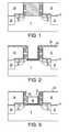
- FIG. 1is a side cross-sectional view depicting forming a replacement gate structure overlying a channel region of a substrate, forming a source region and a drain region on opposing sides of the replacement gate structure, and forming a mandrel dielectric layer overlying the source region and the drain region of the substrate, in accordance with one embodiment of the present disclosure.
- FIG. 2is a side cross-sectional view depicting removing the replacement gate structure to provide an opening exposing the channel region of the substrate, forming a gate dielectric layer on at least the channel region of the substrate, and forming a work function metal layer on the gate dielectric layer, in accordance with one embodiment of the present disclosure.
- FIG. 3is a side cross-sectional view depicting forming a metal fill material on the work function metal layer thus forming a functional gate structure, in accordance with one embodiment of the present disclosure.
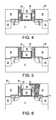
- FIG. 4is a side cross-sectional view depicting forming a protective cap structure over the functional gate structure, in accordance with one embodiment of the present disclosure.
- FIG. 5is a side cross-sectional view depicting planarizing the structure depicted in FIG. 4 to remove at least the gate dielectric layer from an upper surface of the mandrel dielectric layer, in accordance with one embodiment of the present disclosure.
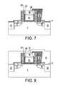
- FIG. 6is a side cross-sectional view depicting etching a via through the mandrel dielectric layer selective to the protective cap structure and the protective dielectric layer to expose at least one of the source region and the drain region, and filling the via to provide a contact to at least one of the source region and the drain region, in accordance with one embodiment of the present disclosure.
- FIG. 7is a side cross-sectional view depicting removing the mandrel dielectric layer, in accordance with one embodiment of the present disclosure.
- FIG. 8is a side cross-sectional view depicting forming a stress-inducing layer overlying the functional gate structure, in accordance with one embodiment of the present disclosure.
- references in the specification to “one embodiment”, “an embodiment”, “an example embodiment”, etc.,indicate that the embodiment described may include a particular feature, structure, or characteristic, but every embodiment may not necessarily include the particular feature, structure, or characteristic. Moreover, such phrases are not necessarily referring to the same embodiment. Further, when a particular feature, structure, or characteristic is described in connection with an embodiment, it is submitted that it is within the knowledge of one skilled in the art to affect such feature, structure, or characteristic in connection with other embodiments whether or not explicitly described.
- the terms “upper”, “lower”, “right”, “left”, “vertical”, “horizontal”, “top”, “bottom”, and derivatives thereofshall relate to the invention, as it is oriented in the drawing figures.
- the terms “overlying”, “atop”, “positioned on” or “positioned atop”mean that a first element, such as a first structure, is present on a second element, such as a second structure, wherein intervening elements, such as an interface structure may be present between the first element and the second element.
- the term “direct contact”means that a first element, such as a first structure, and a second element, such as a second structure, are connected without any intermediary conducting, insulating or semiconductor layers at the interface of the two elements.
- the present disclosurerelates to structures and methods for forming semiconductor devices including gate structures having work function metal layers present therein, in which the contacts to the source and drain regions of the device are formed using a self aligning process.
- semiconductor devicerefers to an intrinsic semiconductor material that has been doped, i.e., into which a doping agent has been introduced, giving it different electrical properties than the intrinsic semiconductor. Doping involves adding dopant atoms to an intrinsic semiconductor, which changes the electron and hole carrier concentrations of the intrinsic semiconductor at thermal equilibrium. Dominant carrier concentrations in an extrinsic semiconductor classify it as either an n-type or p-type semiconductor.
- p-type semiconductorrefers to the addition of trivalent impurities to a semiconductor material that create deficiencies of valence electrons, such as boron, aluminum or gallium to an intrinsic silicon substrate.
- n-type semiconductorrefers to the addition of pentavalent impurities to a semiconductor substrate that contribute free electrons, such as antimony, arsenic or phosphorous to an intrinsic Si substrate.
- FIG. 1depicts an initial structure suitable for use in one embodiment of the present disclosure.
- the initial structuremay include a substrate 5 , source region 10 , drain region 15 , isolation region 20 , metal semiconductor alloy contact 14 , a replacement gate structure 4 , and protective dielectric layers 18 that are present on sidewalls of the replacement gate structure 4 .
- the substrate 5is a bulk substrate that may include, but is not limited to Si-containing materials, GaAs, InAs and other like semiconductors.
- Si-containing materials as used to provide the substrate 5include, but are not limited to Si, bulk Si, single crystal Si, polycrystalline Si, SiGe, amorphous Si, silicon-on-insulator substrates (SOI), SiGe-on-insulator (SGOI), strained-silicon-on-insulator, annealed poly Si, and poly Si line structures.
- SOIsilicon-on-insulator substrates
- SGOISiGe-on-insulator
- strained-silicon-on-insulatorannealed poly Si
- annealed poly Siannealed poly Si
- poly Si line structuressilicon-on-insulator substrates
- Si-containing materialsdenotes any semiconductor material that includes silicon.
- the substrate 5may also be Ge, Ge alloys, GaAs, InAs, InP as well as other III/V and II/VI compound semiconductors. Combinations of the aforementioned materials can also be used.
- the substrate 5may also be composed of a semiconductor-on-insulator substrate (SOI) which includes a bottom semiconductor-containing layer, a buried insulating layer present atop the bottom semiconductor-containing layer, and top semiconductor-containing layer (i.e., SOI layer) present atop the surface of the buried insulating layer.
- SOIsemiconductor-on-insulator substrate
- the bottom and top semiconductor-containing layersmay be composed of a Si-containing material.
- the buried insulating layermay be a buried oxide region.
- the isolation region 20may be a shallow trench isolation (STI) region formed by etching a trench into the substrate 5 and filling the trench with a dielectric material.
- the etching stepmay be performed utilizing a dry etching process, such as reactive-ion etching, ion beam etching, laser ablation or any combination thereof.
- Chemical vapor deposition (CVD) or another like deposition processcan be used to fill the trench with an STI dielectric material, such as a high-density plasma (HDP) oxide or TEOS (tetraethylorthosilicate).
- the isolation region 20may also be formed by local oxidation (LOCOS) or by an oxide mesa formation process.
- LOClocal oxidation
- a replacement gate structure 4is formed overlying a channel region of the substrate 5 .
- a “replacement gate structure”is a material having a geometry and location on the substrate 5 that determines the location for the later formed functional gate structure that is substituted for the replacement gate structure once the replacement gate structure has been removed.
- the material that provides the replacement gate structuremay be any material that can occupy the space in which the subsequently formed functional gate structure is to be positioned.
- the replacement gate structure 4includes a sacrificial layer that may be composed of a semiconductor-containing material, dielectric material or may be composed of photoresist.
- the replacement gate structure 4in which the replacement gate structure 4 is composed of a semiconductor-containing material, the semiconductor-containing material may be a silicon-containing material.
- the term “silicon-containing material” as used hereindenotes any semiconductor material that includes silicon.
- the semiconductor-containing material that provides the replacement gate structure 4is polysilicon.
- Other illustrative examples of various silicon semiconductor materials that are suitable for the replacement gate structure 4include, but are not limited to: Si, SiGe, SiGeC, SiC and other like Si-containing materials.
- the semiconductor-containing material for the replacement gate structure 4may also be a germanium-containing material.
- the semiconductor-containing materialmay be doped or un-doped.
- the semiconductor-containing materialmay be formed using a deposition process, including but not limited to: low pressure chemical vapor deposition or room temperature chemical vapor deposition.
- the replacement gate structure 4may also be composed of a dielectric material.
- dielectric materials that are suitable for the replacement gate structureinclude nitrides, oxides or oxynitride materials.
- the dielectric material of the replacement gate structure 4may be deposited by chemical vapor deposition (CVD). Variations of CVD processes suitable for depositing the replacement gate structure 4 include, but are not limited to, Atmospheric Pressure CVD (APCVD), Low Pressure CVD (LPCVD) and Plasma Enhanced CVD (EPCVD), Metal-Organic CVD (MOCVD) and combinations thereof.
- APCVDAtmospheric Pressure CVD
- LPCVDLow Pressure CVD
- EPCVDPlasma Enhanced CVD
- MOCVDMetal-Organic CVD
- the replacement gate structure 4is composed of silicon nitride.
- the replacement gate structure 4is composed of an oxide, such as silicon oxide.
- the replacement gate structure 4may also be a multi-layered structure that is composed of semiconductor-containing and dielectric layers, wherein the selection of the composition of the dielectric layers may be selected to provide etch stop layers to facilitate etching during the pattern steps that provide the replacement gate structure 4 .
- the material layers that provide the replacement gate structure 4can be patterned using photolithography and etch processes. More specifically, a pattern is produced by applying a photoresist to the surface to be etched, exposing the photoresist to a pattern of radiation, and then developing the pattern into the photoresist utilizing a resist developer. Once the patterning of the photoresist is completed, the sections covered by the photoresist are protected while the exposed regions are removed using a selective etching process that removes the unprotected regions.
- selectivein reference to a material removal process denotes that the rate of material removal for a first material is greater than the rate of removal for at least another material of the structure to which the material removal process is being applied.
- the patterned resistis then removed using an O 2 ash process, or the patterned resist may be stripped using a wet chemical process.
- the replacement gate structure 4has a width ranging from 10 nm to 20 nm and a height ranging from 40 nm to 100 nm. In yet another embodiment, the gate structure 4 has a width ranging from 15 nm to 20 nm and a height ranging from 60 nm to 80 nm. It is noted that the dimensions for the replacement gate structure are provided for illustrative purposes and are not intended to limit the present disclosure.
- source regions 10 and drain regions 15are formed on opposing sides of the replacement gate structure 4 .
- a drain region 15is the doped region in semiconductor device that is located at an end of the channel in which carriers are flowing out of the semiconductor device, e.g., transistor.
- the source region 10is the doped region in the semiconductor device in which majority carriers are flowing into the channel.
- the channelis the region underlying the functional gate structure and between the source region and the drain region of a semiconductor device that becomes conductive when the semiconductor device is turned on.
- the source regions 10 and drain regions 15are implanted with an n-type dopant, in which the semiconductor device is an n-type conductivity field effect transistor (nFET).
- n-type FET devicesare produced by doping the silicon-containing substrate 5 with elements from group V of the Periodic Table of Elements.
- the group V elementis phosphorus, antimony or arsenic.
- the source regions 10 and drain regions 15are implanted with a p-type dopant, in which the second conductivity type semiconductor device 30 is a p-type conductivity field effect transistor (nFET).
- P-type field effect transistor (pFET) devicesare produced by doping the silicon-containing substrate 5 with elements from group III of the Periodic Table of Elements.
- the group III elementis boron, aluminum, gallium or indium.
- the source regions 10 and drain regions 15may be doped using ion implantation. Resulting dopant concentrations for the source regions 10 and drain regions 15 may range from 1 ⁇ 10 18 dopant atoms per cubic centimeter to 1 ⁇ 10 21 dopant atoms per cubic centimeter.
- the source regions 10 and drain regions 15may further include extension regions and/or halo implant regions (not shown).
- the implants to provide the extension regions and the halo implant regionsmay include a combination of normally incident and angled implants to form the desired grading and implant depth.
- FIG. 1further depicts forming a protective dielectric layer 18 on the sidewalls of the replacement gate structure 4 .
- the protective dielectric layer 18is selected to provide a material that will not be substantially etched by the etchant that provides the opening through the mandrel dielectric to the source regions 10 and drain regions 15 .
- the protective dielectric layer 18is provided by at least one spacer.
- the at least one spacermay be formed on the sidewall of the replacement gate structure 4 using deposition and etch processes.
- the at least one spacerhas a width measured at the base of the at least one spacer ranging from 3 nm to 40 nm.
- the at least one spacerhas a width measured at the base of the at least one spacer ranging from 20.0 nm to 30.0 nm.
- the at least one spacer's widthmay taper, i.e., may reduce, in the direction from the semiconductor substrate 5 towards the upper surface of the replacement gate structure 4 .
- the protective dielectric layermay be comprised of a dielectric material, such as a nitride, e.g., silicon nitride.
- the protective dielectric layermay be comprised of a low-k dielectric material, which typically has a dielectric constant that is less than 4.0, e.g., 3.9.
- the protective dielectric layer 18is comprised of a low-k dielectric material having a dielectric constant ranging from 1.75 to 3.5.
- low-k dielectricexamples include organosilicate glass (OSG), fluorine doped silicon dioxide, carbon doped silicon dioxide, porous silicon dioxide, porous carbon doped silicon dioxide, spin-on organic polymeric dielectrics (e.g., SILKTM), spin-on silicone based polymeric dielectric (e.g., hydrogen silsesquioxane (HSQ) and methylsilsesquioxane (MSQ), and combinations thereof.
- OSGorganosilicate glass
- fluorine doped silicon dioxidecarbon doped silicon dioxide
- porous silicon dioxideporous carbon doped silicon dioxide
- spin-on organic polymeric dielectricse.g., SILKTM
- spin-on silicone based polymeric dielectrice.g., hydrogen silsesquioxane (HSQ) and methylsilsesquioxane (MSQ)
- the material of the at least one spacer that provides the protective dielectric layer 18is selected to protect the subsequently formed functional gate structure during the process steps that provide the opening for the contact.
- the spacermay be a nitride, such as silicon nitride, when the subsequently formed protective cap structure is composed of a nitride, such as silicon nitride, and the subsequently formed mandrel dielectric is composed of boron phosphorus silicate glass (BPSG).
- BPSGboron phosphorus silicate glass
- Metal semiconductor alloy regions 14may be formed atop the source regions 10 and the drain regions 15 .
- a “metal semiconductor alloy”is an alloy of a metal and a semiconductor.
- the metal semiconductor alloy regions 14are composed of a silicide.
- Silicide formationtypically requires depositing a metal layer onto the surface of a Si-containing material or wafer.
- the metal layermay be deposited by at least one of chemical vapor deposition (CVD), plasma-assisted CVD, high-density chemical vapor deposition (HDCVD), plating, sputtering, evaporation and chemical solution deposition.
- Metals deposited for silicide formationinclude Ta, Ti, W, Pt, Co, Ni, and combinations thereof.
- the structureis subjected to an annealing step, which may include rapid thermal annealing.
- the deposited metalreacts with Si forming a metal silicide.
- the metal semiconductor alloy 14may also be a germinide, i.e., germanium and silicon alloy.
- a passivation layer 6may be formed in direct contact with an upper surface of the metal semiconductor alloy regions 14 , the isolation regions 20 , and a sidewall surface of the protective dielectric layer 18 .
- the passivation layer 6may be formed using thermal growth, e.g., thermal oxidation, or deposition processes, e.g., chemical vapor deposition.
- the passivation layer 6may be composed of an oxide, nitride or oxynitride material. In one embodiment, the passivation layer 6 is composed of silicon oxide.
- the passivation layer 6may have a thickness ranging from 3.0 nm to 25.0 nm.
- FIG. 1further depicts one embodiment of forming a mandrel dielectric layer 25 overlying the source region 10 and the drain region 15 of the substrate 5 .
- the mandrel dielectric layer 25has an upper surface that is coplanar with an upper surface of the replacement gate structure 4 .
- the composition for the mandrel dielectric layer 25is selected to protect the subsequently formed functional gate structure during the process steps that provide the opening for the contact.
- the mandrel dielectric layer 25may be selected from the group consisting of silicon-containing materials such as SiO 2 , Si 3 N 4 , SiO x N y , SiC, SiCO, SiCOH, and SiCH compounds, the above-mentioned silicon-containing materials with some or all of the Si replaced by Ge, carbon-doped oxides, inorganic oxides, inorganic polymers, hybrid polymers, organic polymers such as polyamides or SiLKTM, other carbon-containing materials, organo-inorganic materials such as spin-on glasses and silsesquioxane-based materials, and diamond-like carbon (DLC, also known as amorphous hydrogenated carbon, ⁇ -C:H).
- silicon-containing materialssuch as SiO 2 , Si 3 N 4 , SiO x N y , SiC, SiCO, SiCOH, and SiCH compounds
- the above-mentioned silicon-containing materials with some or all of the Si replaced by Gecarbon-doped oxides, inorganic oxide
- mandrel dielectric layer 25includes: any of the aforementioned materials in porous form, or in a form that changes during processing to or from being porous and/or permeable to being non-porous and/or non-permeable.
- the blanket layer of the mandrel dielectric layer 25may be formed by deposition processes, including, but not limited to spinning from solution, spraying from solution, chemical vapor deposition (CVD), plasma enhanced CVD (PECVD), sputter deposition, reactive sputter deposition, ion-beam deposition, and evaporation.
- the mandrel dielectric layer 25is planarized until the upper surface of the replacement gate structure 4 has been exposed.
- Planarizationis a material removal process that employs at least mechanical forces, such as frictional media, to produce a planar surface.
- CMPchemical mechanical planarization
- CMPis a material removal process using both chemical reactions and mechanical forces to remove material and planarize a surface.
- FIG. 2depicts removing the replacement gate structure 4 to provide an opening exposing the channel region of the substrate 5 .
- the replacement gate structure 4is typically removed using a selective etch process that removes the replacement gate structure 4 selective to the substrate 5 , the mandrel dielectric layer 25 , and the protective dielectric layer 18 .
- the etchmay be an isotropic etch, such as a wet etch, or an anisotropic etch, such as reactive ion etching.
- An isotropic etch processis a material removal process in which the rate of the etching reaction is substantially similar in any direction.
- An anisotropic etch processis a material removal process in which the etch rate in the direction normal to the surface to be etched is much higher than in the direction parallel to the surface to be etched.
- “Reactive Ion Etching”is a form of plasma etching, in which during etching the surface to be etched is placed on the RF powered electrode, wherein the surface to be etched takes on a potential that accelerates the etching species extracted from a plasma towards the surfaces, to be etched, in which the chemical etching reaction is taking place in the direction normal to the surface.
- the replacement gate structure 4is composed of polysilicon
- the substrate 5is a silicon-containing material
- the mandrel dielectric 25is composed of boron phosphorus silicate glass
- the protective dielectric layer 18is composed of silicon nitride
- the wet etch chemistrymay be composed of NH 4 OH or tetramethylammonium hydroxide (TMAH).
- FIG. 2further depicts forming a gate dielectric layer 30 on at least the channel region of the substrate 5 , and forming a work function metal layer 35 on the gate dielectric layer 30 .
- the gate dielectric layer 30is formed using a deposition process, such as chemical vapor deposition.
- Chemical Vapor Deposition (CVD)is a deposition process in which a deposited species is formed as a results of a chemical reaction between gaseous reactants at an elevated temperature (typically being greater than 600° C.), wherein solid product of the reaction is deposited on the surface on which a film, coating, or layer of the solid product is to be formed.
- CVD processesinclude, but are not limited to, Atmospheric Pressure CVD (APCVD), Low Pressure CVD (LPCVD) and Plasma Enhanced CVD (EPCVD), Metal-Organic CVD (MOCVD) and others.
- APCVDAtmospheric Pressure CVD
- LPCVDLow Pressure CVD
- EPCVDPlasma Enhanced CVD
- MOCVDMetal-Organic CVD
- the gate dielectric layer 30may be formed by a thermal growth process such as, for example, oxidation, nitridation or oxynitridation.
- the gate dielectric layer 30is a conformal dielectric layer that is present on the sidewalls of the opening that is formed by removing the replacement gate structure and the base of the opening, i.e., channel region of the substrate 5 .
- the conformal dielectric layeris also present on the upper surface of the mandrel dielectric 25 and the upper surface of the protective dielectric layer 18 .
- the term “conformal”denotes a layer having a thickness that does not deviate from greater than or less than 30% of an average value for the thickness of the layer.
- the thickness of the gate dielectric layer 30typically ranges from 1 nm to 10 nm. In one embodiment, the thickness of the gate dielectric layer 30 ranges from 2 nm to 5 nm.
- the gate dielectric layer 30may be composed of any dielectric including, but not limited to SiO 2 ; Si 3 N 4 ; SiON; temperature sensitive high-k dielectrics such as TiO 2 , Al 2 O 3 , ZrO 2 , HfO 2 , Ta 2 O 5 , La 2 O 3 ; and other like oxides including perovskite-type oxides.
- the gate dielectric layer 30may also be a high-k dielectric.
- the high-k dielectricmay be composed of an oxide, a nitride, an oxynitride or combinations and multi-layers thereof.
- a high-k dielectricmay be a material having a dielectric constant that is greater than the dielectric constant of silicon oxide.
- the high-k dielectricis comprised of a material having a dielectric constant that is greater than 4.0, e.g., 4.1.
- the high-k dielectricis comprised of a material having a dielectric constant greater than 7.0.
- the high-k dielectricis comprised of a material having a dielectric constant ranging from greater than 4.0 to 30.
- the dielectric constants mentioned hereinare relative to a vacuum.
- high-k dielectric materials suitable for the gate dielectric layer 30include hafnium oxide, hafnium silicon oxide, hafnium silicon oxynitride, lanthanum oxide, lanthanum aluminum oxide, zirconium oxide, zirconium silicon oxide, zirconium silicon oxynitride, tantalum oxide, titanium oxide, barium strontium titanium oxide, barium titanium oxide, strontium titanium oxide, yttrium oxide, aluminum oxide, lead scandium tantalum oxide, lead zinc niobate and combinations thereof.
- the gate dielectric layer 30has a thickness ranging from 1.0 nm to 10.0 nm.
- the gate dielectric layer 30may have a thickness ranging from 2.5 nm to 5.0 nm.
- the gate dielectric layer 30is hafnium oxide (HfO 2 ).
- gate dielectric layer 30is a multi-layered structure that is composed of a high-k dielectric layer and a metal nitride gate dielectric.
- the metal nitride gate dielectricis composed of WN, WSiN, TiN, TiSiN, TaN, TaSiN, TiTaN, TaRuN or combinations thereof.
- the work function metal layer 35may be conformally deposited on the gate dielectric layer 30 .
- the gate dielectric layer 30is composed of a high-k material
- the work function metal layer 35is in direct contact with the portion of the high-k gate dielectric layer 30 that is present on the channel portion of the substrate 5
- the work function metal layer 35is in direct contact with the portion of the high-k gate dielectric layer 30 that is present on the sidewall portion of opening that is produced by removing the replacement gate structure 4 .
- the thickness of the work function metal layer 35typically ranges from 1.0 nm to 10.0 nm. In another example, the thickness of the work function metal layer 35 may range from 2.5 nm to 5.0 nm.
- the work function metal layer 35may be a p-type work function metal layer.
- a “p-type work function metal layer”is a metal layer that effectuates a p-type threshold voltage shift.
- the work function of the p-type work function metal layerranges from 4.9 eV to 5.2 eV.
- threshold voltageis the lowest attainable gate voltage that will turn on a semiconductor device, e.g., transistor, by making the channel of the device conductive.
- p-type threshold voltage shiftmeans a shift in the Fermi energy of a p-type semiconductor device towards a valence band of silicon in the silicon containing substrate of the p-type semiconductor device.
- a “valence band”is the highest range of electron energies where electrons are normally present at absolute zero.
- the p-type work function metal layeris composed of titanium aluminum nitride (TiAlN).
- TiAlNtitanium aluminum nitride
- the titanium content of the titanium aluminum nitride (TiAlN)may range from 20 wt % to 80 wt %
- the aluminum content of the titanium aluminum nitridemay range from 20 wt % to 60 wt %
- the nitrogen content of the titanium aluminum nitridemay range from 20 wt % to 60 wt %.
- the titanium content of the titanium aluminum nitridemay range from 30 wt % to 60 wt %, the aluminum content of the titanium aluminum nitride may range from 25 wt % to 40 wt %, and the nitrogen content of the titanium aluminum nitride may range from 25 wt % to 50 wt %.
- a sputtering deposition process for depositing titanium aluminum nitrideincludes applying high energy particles to strike a solid slab of a titanium aluminum alloy target material, in which the high energy particles physically dislodge atoms of titanium and aluminum to be deposited on at least the gate dielectric layer 30 .
- the sputtering apparatusmay include dual targets, e.g., a first target composed of titanium and a second target composed of aluminum. The sputtered atoms of titanium and aluminum typically migrate through a vacuum and deposit on the deposition surface.
- the ion energies of the high-energy particlese.g., positive ions from an argon gas flow discharge range from 500 eV to 5,000 eV. In another embodiment, the ion energies of the high-energy particles range from 1,500 eV to 4,500 eV.
- Other materials that are suitable for providing the p-type work function metal layerinclude TaC, TaNC, Ru, and TiNi.
- the work function metal layer 35may be an n-type work function metal layer.
- the work function of the n-type work function metal layerranges from 4.1 eV to 4.3 eV.
- a “n-type work function metal layer”is a metal layer that effectuates an n-type threshold voltage shift.
- N-type threshold voltage shiftas used herein means a shift in the Fermi energy of an n-type semiconductor device towards a conduction band of silicon in a silicon-containing substrate of the n-type semiconductor device.
- the “conduction band”is the lowest lying electron energy band of the doped material that is not completely filled with electrons.
- the n-type work function metal layeris composed of TiN.
- a sputtering deposition process for depositing titanium nitrideincludes applying high energy particles to strike a solid slab of a titanium nitride target material, in which the high energy particles physically dislodge particles of titanium nitride to be deposited on at least the gate dielectric layer 30 .
- TiNis sputtered from a solid titanium target, in which the nitrogen content of the metal nitride layer is introduced by a nitrogen gas.
- the sputtered atoms of titanium and nitrogentypically migrate through a vacuum and deposit on the gate dielectric layer 30 .
- the ion energies of the high-energy particlese.g., positive ions from an argon gas flow discharge range from 500 eV to 5,000 eV. In another embodiment, the ion energies of the high-energy particles range from 1,500 eV to 4,500 eV.
- Other materials that are suitable for providing the n-type work function metal layerinclude TiN, TiAl, TiAl/TiN, AlN/TiN or combinations thereof.
- FIG. 3depicts forming a metal fill material 40 on the work function metal layer 35 .
- the metal fill material 40is composed of aluminum.
- a sputtering deposition process for depositing the metal fill material 40 that is composed of aluminumincludes applying high energy particles to strike a solid slab of high-purity aluminum target material, in which the high energy particles physically dislodge atoms of the aluminum to be deposited on the work function metal layer 35 .
- the ion energies of the high-energy particlese.g., positive ions from an argon gas flow discharge, range from 500 eV to 5,000 eV. In another embodiment, the ion energies of the high-energy particles range from 1,500 eV to 4,500 eV.
- high-purity aluminumit is meant that the aluminum content of the target material is greater than 99.5%. In some embodiments, the aluminum content of the target material may be as great as 99.9% with a remainder of incidental impurities.
- incidental impuritiesdenote any contamination of the target, i.e., aluminum. Allowable ranges of impurities are less than 0.05 wt % for each impurity constituent, and 0.1 wt % for total impurity content.
- the sputtered aluminum atoms from the aluminum targetmay migrate through a vacuum and deposit on the deposition surface, e.g., the work function metal layer 35 .
- iron (Fe), copper (Cu), and silver (Ag)may be present in less than 5 parts per million (ppm).
- the metal fill material 40 comprising aluminummay be planarized until an upper surface of the metal fill material 40 is coplanar with an upper surface of the mandrel dielectric layer 25 .
- the planarization processis provided by chemical mechanical planarization (CMP).
- the metal fill material 40 , work function metal layer 35 and the gate dielectric layer 30provide a functional gate structure.
- the term “functional gate structure”means a structure used to control output current (i.e., flow of carriers in the channel) of a semiconducting device through electrical or magnetic fields.
- the metal fill material 40may be recessed below the upper surface of the mandrel dielectric layer 25 and the protective dielectric layer 18 .
- the metal fill material 40may be recessed using an etch process that is selective to the work function metal layer 35 .
- the etch processmay be an anisotropic etch, such reactive ion etch (RIE), or the etch process may be an isotropic etch, such as a wet etch.
- RIEreactive ion etch
- the etch chemistry that etches the metal fill material 40 selective to the work function metal layer 35produces a surface dielectric layer 50 , such as an oxide layer, on the recessed surface of the metal fill material 40 .
- the surface dielectric layer 50is composed of silicon oxide.
- the surface dielectric layer 50may have a thickness ranging from 2 nm to 5 nm.
- the work function metal layer 35may be removed from the upper surface of the mandrel dielectric layer 25 , the upper surface of the protective dielectric layer 18 , by a selective etch process.
- the selective etch processmay also remove a portion of the work function metal layer 35 that is present on the sidewalls of an upper portion of the opening.
- the upper portion of the opening from which the work function metal layer 35 is removedextends to a depth that is substantially equal to or below the surface dielectric layer 50 .
- a remaining portion of the work function metal layer 35is present in a lower portion of the opening.
- the etch process that removes the work function metal layer 35may be an isotropic etch, such as a wet etch, or may be an anisotropic etch, such as reactive ion etch.
- the etch chemistry that removes the work function metal layer 35is selective to the gate dielectric layer 30 and the surface dielectric layer 50 .
- the etch chemistry that removes the work function metal layer 35is composed of NH 4 OH:H 2 O 2 .
- FIG. 4depicts forming a protective cap structure 60 over the functional gate structure.
- the protective cap structure 60is composed of a dielectric material, and fills the upper portion of the opening that is present over the recessed surface of the metal fill 40 .
- the protective cap structure 60may be composed of any dielectric material that can protect the functional gate from being damaged during the etch process that provides the openings to the source regions 10 and the drain regions 15 .
- the protective cap structure 60is typically composed of at least one of an oxide, nitride or oxynitride material.
- the protective dielectric layer 18is composed of a nitride, such as silicon nitride
- the mandrel dielectric layer 25is composed of boron phosphorus silicate glass (BPSG)
- the protective cap structure 60is composed of a nitride, such as silicon nitride.
- the protective cap structure 60may be formed by a deposition process including, but not limited to spinning from solution, spraying from solution, and chemical vapor deposition (CVD). Variations of CVD processes include, but are not limited to, Atmospheric Pressure CVD (APCVD), Low Pressure CVD (LPCVD) and Plasma Enhanced CVD (EPCVD), Metal-Organic CVD (MOCVD), high-density chemical vapor deposition (HDCVD) and others.
- APCVDAtmospheric Pressure CVD
- LPCVDLow Pressure CVD
- EPCVDPlasma Enhanced CVD
- MOCVDMetal-Organic CVD
- HDCVDhigh-density chemical vapor deposition
- the dielectric material that provides the protective cap structure 60may be planarized stopping on the gate dielectric layer 30 that is present on an upper surface of the mandrel dielectric layer 25 .
- the planarization processis provided by chemical mechanical planarization (CMP).
- CMPchemical mechanical planarization
- the planarization processmay be continued until the gate dielectric layer 30 is removed from the upper surface of the mandrel dielectric layer 25 , as depicted in FIG. 5 .
- FIG. 6depicting etching a via 75 through the mandrel dielectric layer 25 using an etch process that is selective to the protective cap structure 60 and the protective dielectric layer 18 to expose at least one of the source region 10 and the drain region 15 .
- the viaexposes the drain region.
- the viaexposes the source region 10 .
- an interlevel dielectric layer 85is blanket deposited atop the structure depicted in FIG. 5 .
- the interlevel dielectric layer 85may be selected from the group consisting of silicon-containing materials such as SiO 2 , Si 3 N 4 , SiO x N y , SiC, SiCO, SiCOH, and SiCH compounds, the above-mentioned silicon-containing materials with some or all of the Si replaced by Ge, carbon-doped oxides, inorganic oxides; inorganic polymers; hybrid polymers; organic polymers such as polyamides or SiLKTM, other carbon-containing materials; organo-inorganic materials such as spin-on glasses and silsesquioxane-based materials, and diamond-like carbon (DLC, also known as amorphous hydrogenated carbon, ⁇ -C:H). Additional choices for the interlevel dielectric layer 85 include: any of the aforementioned materials in porous form, or in a form that changes during processing to or from being porous and/or permeable to being non-porous and/or non-permeable.
- silicon-containing materialssuch as SiO 2 , Si 3 N 4
- the interlevel dielectric layer 85may be formed by various methods well known to those skilled in the art, including, but not limited to: spinning from solution, spraying from solution, chemical vapor deposition (CVD), plasma enhanced CVD (PECVD), sputter deposition, reactive sputter deposition, ion-beam deposition, and evaporation.
- CVDchemical vapor deposition
- PECVDplasma enhanced CVD
- sputter depositionreactive sputter deposition
- ion-beam depositionion-beam deposition
- the interlevel dielectric layer 85 and the mandrel dielectric layer 25are then patterned and etched to form vias 75 to the source regions 10 and the drain regions 15 using patterning and selective etch process. More specifically, a pattern is produced by applying a photoresist to the surface to be etched, exposing the photoresist to a pattern of radiation, and then developing the pattern into the photoresist utilizing a resist developer. Once the patterning of the photoresist is completed, the sections covered by the photoresist are protected while the exposed regions are removed using a selective etching process that removes the unprotected regions to provide the vias 75 .
- the vias 75typically have a width ranging from 20 nm to 100 nm. In another embodiment, the vias 75 have a width ranging from 40 nm to 80 nm.
- the etch chemistry that provides the vias 75removes at least the material of the mandrel dielectric layer 25 selective to the protective cap structure 60 and the protective dielectric layer 18 , wherein the protective cap structure 60 and the protective dielectric layer 18 protect the functional gate structure from being damaged by the via 75 etch.
- contacts 90are formed by depositing a conductive metal into the vias 75 using deposition processing, such as CVD or plating.
- the conductive metalmay include, but is not limited to tungsten, copper, aluminum, silver, gold, and alloys thereof.
- the contacts 90are self-aligned to the diffusion regions, i.e., source regions 10 and drain regions 15 , because the functional gate is protected from being damaged by the etch process that forms the vias 75 for the contacts 90 by the protective cap structure 60 that is present over the functional gate, and the protective dielectric layer 18 that is present on the sidewall of the functional gate.
- FIG. 7depicts one embodiment of removing the mandrel dielectric layer 25 .
- the mandrel dielectric layer 25may be removed by an etch process that removes the mandrel dielectric layer 25 selective to at least the contacts 90 , the protective cap structure 60 , the protective dielectric layer 18 , and the passivation layer 6 .
- the etchmay be an isotropic etch, such as a wet etch, or an anisotropic etch, such as reactive ion etching.
- FIG. 8depicts forming a stress-inducing layer 95 overlying the functional gate structure.
- stress inducing layerdenotes a material having an intrinsic stress, in which the intrinsic stress effectuates a stress in an underlying material.
- the stress-inducing layer 95may be a non-conformal layer.
- non-conformaldenotes a layer having a thickness that deviates by greater than or equal to 30% of an average value for the thickness of the layer.
- the stress-inducing layer 95is non-conformal because it is formed after the contacts 90 to the source regions 10 and drain regions 15 . Typically, in prior methods and structures, the stress-inducing layer 95 is formed prior to forming the contacts.
- the stress-inducing layer 95may be a tensile stress-inducing layer or a compressive stress-inducing layer.
- the stress-inducing layer 95is a tensile stress-inducing layer that is formed overlying at least the functional gate to an n-type semiconductor device, e.g., n-type field effect transistor (nFET).
- nFETn-type field effect transistor
- tensile stress inducing materialdenotes a material layer having an intrinsic tensile stress, in which the intrinsic tensile stress produces a tensile stress in an underlying material.
- the stress-inducing layer 95is a compressive stress inducing layer that is formed overlying at least the functional gate to an p-type semiconductor device, e.g., p-type field effect transistor (pFET).
- pFETp-type field effect transistor
- the term “compressive stress inducing material”denotes a material having an intrinsic compressive stress, in which the intrinsic compressive stress produces a compressive stress in an underlying material.
- the tensile stress-inducing layermay be any material that is capable of introducing a tensile stress into the device channel that is underlying the functional gate structure.
- stress inducing materialsinclude, but are not limited to: Si 3 N 4 , SiC, silicon oxynitride and other like materials.
- the tensile stress inducing layeris comprised of Si 3 N 4 .
- the tensile stress inducing layercan be formed utilizing various chemical vapor deposition (CVD) processes including, for example, low pressure CVD, plasma enhanced CVD, rapid thermal CVD, BTBAS-based (C 8 H 22 N 2 Si reacted with ammonia) CVD, where BTBAS is a modern metalorganic precursor for CVD applications.
- CVDchemical vapor deposition
- PECVDPlasma enhanced chemical vapor deposition
- HDCVDhigh density chemical vapor deposition
- the stress state of nitride-containing tensile stress inducing layer deposited by PECVDcan be controlled by changing the deposition conditions to alter the reaction rate within the deposition chamber. More specifically, the stress state of a tensile stress inducing layer comprised of silicon nitride may be set by changing the deposition conditions such as: SiH 4 /N 2 /He gas flow rate, pressure, RF power, and electrode gap.
- Rapid thermal chemical vapor depositioncan provide nitride-containing tensile stress inducing layer.
- the magnitude of the internal tensile stress produced within nitride-containing tensile stress inducing layer deposited by RTCVDcan be controlled by changing the deposition conditions. More specifically, the magnitude of the tensile stress within strain tensile stress inducing layer comprised of silicon nitride may be set by changing deposition conditions such as: precursor composition, precursor flow rate and temperature.
- the tensile stress inducing layermay have an as-deposited thickness from 20 nm to 150 nm. In another embodiment, the as-deposited thickness of the tensile stress inducing layer ranges from 30 nm to 100 nm.
- the tensile stress inducing layermay include a stress having a magnitude ranging from 1 GPa to 1.6 GPa on the channel of the device.
- the compressive stress inducing layer 22may be any material that is capable of introducing a compressive stress into the device channel that is underlying the second gate stack 25 .
- stress inducing materialsinclude, but are not limited to: Si 3 N 4 , SiC, silicon oxynitride and other like materials.
- the compressive stress inducing layer 22is comprised of Si 3 N 4 .
- the compressive stress inducing layer 22can be formed utilizing various chemical vapor deposition (CVD) processes including, for example, low pressure CVD, plasma enhanced CVD, rapid thermal CVD, BTBAS-based (C 8 H 22 N 2 Si reacted with ammonia) CVD, where BTBAS is a modern metalorganic precursor for CVD applications.
- CVDchemical vapor deposition
- PECVDPlasma enhanced chemical vapor deposition
- HDCVDhigh density chemical vapor deposition
- the stress state of nitride-containing compressive stress inducing layer deposited by PECVDcan be controlled by changing the deposition conditions to alter the reaction rate within the deposition chamber. More specifically, the stress state of a compressive stress inducing layer comprised of silicon nitride may be set by changing the deposition conditions such as: SiH 4 /N 2 /He gas flow rate, pressure, RF power, and electrode gap.
- the compressive stress inducing layermay have an as-deposited thickness from 20 nm to 150 nm. In another embodiment, the as-deposited thickness of the compressive stress inducing layer ranges from 30 nm to 100 nm.
- the compressive stress inducing layermay include a stress having a magnitude ranging from 2 Gpa to 3 GPa on the channel of the device.
Landscapes
- Engineering & Computer Science (AREA)
- Microelectronics & Electronic Packaging (AREA)
- Condensed Matter Physics & Semiconductors (AREA)
- General Physics & Mathematics (AREA)
- Manufacturing & Machinery (AREA)
- Computer Hardware Design (AREA)
- Physics & Mathematics (AREA)
- Power Engineering (AREA)
- Chemical & Material Sciences (AREA)
- Composite Materials (AREA)
- Thin Film Transistor (AREA)
- Insulated Gate Type Field-Effect Transistor (AREA)
- Materials Engineering (AREA)
Abstract
Description
- The present disclosure relates to semiconductor devices. More particularly, the present disclosure relates to forming gate structures and interconnects to semiconductor devices.
- Field effect transistors (FETs) are the basic building block of today's integrated circuits (ICs). Such transistors can be formed in conventional bulk semiconductor substrates (such as silicon) or in a SOI layer of a semiconductor-on-insulator (SOI) substrate. In order to be able to make ICs, such as memory, logic, and other devices, of higher integration density than currently feasible, one has to find ways to further downscale the dimensions of field effect transistors (FETs), such as metal-oxide-semiconductor field effect transistors (MOSFETs) and complementary metal oxide semiconductors (CMOS). Scaling achieves compactness and improves operating performance in devices by shrinking the overall dimensions and operating voltages of the device, while maintaining the device's electrical properties.
- The present disclosure provides a method for forming a semiconductor device that includes forming a protective dielectric layer on sidewalls of a replacement gate structure that is present overlying a channel region of a substrate. A source region and a drain region may be formed on opposing sides of the replacement gate structure. A mandrel dielectric layer is formed overlying the source region and the drain region of the substrate. The mandrel dielectric layer has an upper surface that is coplanar with an upper surface of the replacement gate structure. The replacement gate structure is removed to provide an opening exposing the channel region of the substrate. A functional gate structure is formed over the channel region including a work function metal layer. A protective cap structure is formed over the functional gate structure. At least one via is etched through the mandrel dielectric layer selective to the protective cap structure and the protective dielectric layer to expose a portion of at least one of the source region and the drain region. A conductive fill is then formed in the vias to provide a contact to the at least one of the source region and the drain region.
- In another aspect, a semiconductor device is provided that includes a gate structure that includes a work function metal layer, in which the contacts to at least one of the source and the drain region are self aligned, i.e., are not shorted to the gate structure. In one embodiment, the semiconductor device includes a gate structure. The gate structure includes a metal-containing gate conductor present on a work function metal layer, in which the work function metal layer is present on a high-k gate dielectric. The high-k gate dielectric is present on a channel portion of a substrate. A protective cap layer is present over the gate structure. A protective dielectric layer is present on sidewalls of the gate structure. Source and drain regions are present on opposing sides of the channel portion of the substrate. The semiconductor device further comprises a contact to at least one of the source and drain regions, wherein the contact is separated from the gate structure by the protective cap and the protective dielectric layer. A non-conformal stress inducing layer is present over at least the protective cap, the protective dielectric layer, and the source and drain regions.
- The following detailed description, given by way of example and not intended to limit the invention solely thereto, will best be appreciated in conjunction with the accompanying drawings, wherein like reference numerals denote like elements and parts, in which:
FIG. 1 is a side cross-sectional view depicting forming a replacement gate structure overlying a channel region of a substrate, forming a source region and a drain region on opposing sides of the replacement gate structure, and forming a mandrel dielectric layer overlying the source region and the drain region of the substrate, in accordance with one embodiment of the present disclosure.FIG. 2 is a side cross-sectional view depicting removing the replacement gate structure to provide an opening exposing the channel region of the substrate, forming a gate dielectric layer on at least the channel region of the substrate, and forming a work function metal layer on the gate dielectric layer, in accordance with one embodiment of the present disclosure.FIG. 3 is a side cross-sectional view depicting forming a metal fill material on the work function metal layer thus forming a functional gate structure, in accordance with one embodiment of the present disclosure.FIG. 4 is a side cross-sectional view depicting forming a protective cap structure over the functional gate structure, in accordance with one embodiment of the present disclosure.FIG. 5 is a side cross-sectional view depicting planarizing the structure depicted inFIG. 4 to remove at least the gate dielectric layer from an upper surface of the mandrel dielectric layer, in accordance with one embodiment of the present disclosure.FIG. 6 is a side cross-sectional view depicting etching a via through the mandrel dielectric layer selective to the protective cap structure and the protective dielectric layer to expose at least one of the source region and the drain region, and filling the via to provide a contact to at least one of the source region and the drain region, in accordance with one embodiment of the present disclosure.FIG. 7 is a side cross-sectional view depicting removing the mandrel dielectric layer, in accordance with one embodiment of the present disclosure.FIG. 8 is a side cross-sectional view depicting forming a stress-inducing layer overlying the functional gate structure, in accordance with one embodiment of the present disclosure.- Detailed embodiments of the present invention are disclosed herein; however, it is to be understood that the disclosed embodiments are merely illustrative of the invention that may be embodied in various forms. In addition, each of the examples given in connection with the various embodiments of the invention is intended to be illustrative, and not restrictive. Further, the figures are not necessarily to scale, some features may be exaggerated to show details of particular components. Therefore, specific structural and functional details disclosed herein are not to be interpreted as limiting, but merely as a representative basis for teaching one skilled in the art to variously employ the present invention.
- References in the specification to “one embodiment”, “an embodiment”, “an example embodiment”, etc., indicate that the embodiment described may include a particular feature, structure, or characteristic, but every embodiment may not necessarily include the particular feature, structure, or characteristic. Moreover, such phrases are not necessarily referring to the same embodiment. Further, when a particular feature, structure, or characteristic is described in connection with an embodiment, it is submitted that it is within the knowledge of one skilled in the art to affect such feature, structure, or characteristic in connection with other embodiments whether or not explicitly described.
- For purposes of the description hereinafter, the terms “upper”, “lower”, “right”, “left”, “vertical”, “horizontal”, “top”, “bottom”, and derivatives thereof shall relate to the invention, as it is oriented in the drawing figures. The terms “overlying”, “atop”, “positioned on” or “positioned atop” mean that a first element, such as a first structure, is present on a second element, such as a second structure, wherein intervening elements, such as an interface structure may be present between the first element and the second element. The term “direct contact” means that a first element, such as a first structure, and a second element, such as a second structure, are connected without any intermediary conducting, insulating or semiconductor layers at the interface of the two elements.
- The present disclosure relates to structures and methods for forming semiconductor devices including gate structures having work function metal layers present therein, in which the contacts to the source and drain regions of the device are formed using a self aligning process. The term “semiconductor device” refers to an intrinsic semiconductor material that has been doped, i.e., into which a doping agent has been introduced, giving it different electrical properties than the intrinsic semiconductor. Doping involves adding dopant atoms to an intrinsic semiconductor, which changes the electron and hole carrier concentrations of the intrinsic semiconductor at thermal equilibrium. Dominant carrier concentrations in an extrinsic semiconductor classify it as either an n-type or p-type semiconductor. As used herein, “p-type semiconductor” refers to the addition of trivalent impurities to a semiconductor material that create deficiencies of valence electrons, such as boron, aluminum or gallium to an intrinsic silicon substrate. As used herein, “n-type semiconductor” refers to the addition of pentavalent impurities to a semiconductor substrate that contribute free electrons, such as antimony, arsenic or phosphorous to an intrinsic Si substrate.
FIG. 1 depicts an initial structure suitable for use in one embodiment of the present disclosure. The initial structure may include asubstrate 5,source region 10, drain region15,isolation region 20, metalsemiconductor alloy contact 14, a replacement gate structure4, and protectivedielectric layers 18 that are present on sidewalls of the replacement gate structure4.- In one embodiment, the
substrate 5 is a bulk substrate that may include, but is not limited to Si-containing materials, GaAs, InAs and other like semiconductors. Si-containing materials as used to provide thesubstrate 5 include, but are not limited to Si, bulk Si, single crystal Si, polycrystalline Si, SiGe, amorphous Si, silicon-on-insulator substrates (SOI), SiGe-on-insulator (SGOI), strained-silicon-on-insulator, annealed poly Si, and poly Si line structures. The term “Si-containing materials” as used herein denotes any semiconductor material that includes silicon. Illustrative examples of various Si semiconductor materials that can be employed in the present invention include, but are not limited to Si, SiGe, SiGeC, SiC and other like Si-containing materials. Thesubstrate 5 may also be Ge, Ge alloys, GaAs, InAs, InP as well as other III/V and II/VI compound semiconductors. Combinations of the aforementioned materials can also be used. - Although not depicted in the Figures, the
substrate 5 may also be composed of a semiconductor-on-insulator substrate (SOI) which includes a bottom semiconductor-containing layer, a buried insulating layer present atop the bottom semiconductor-containing layer, and top semiconductor-containing layer (i.e., SOI layer) present atop the surface of the buried insulating layer. The bottom and top semiconductor-containing layers may be composed of a Si-containing material. In some embodiments, the buried insulating layer may be a buried oxide region. - At least one
isolation region 20 may be formed in thesubstrate 5. Theisolation region 20 may be a shallow trench isolation (STI) region formed by etching a trench into thesubstrate 5 and filling the trench with a dielectric material. The etching step may be performed utilizing a dry etching process, such as reactive-ion etching, ion beam etching, laser ablation or any combination thereof. Chemical vapor deposition (CVD) or another like deposition process can be used to fill the trench with an STI dielectric material, such as a high-density plasma (HDP) oxide or TEOS (tetraethylorthosilicate). Theisolation region 20 may also be formed by local oxidation (LOCOS) or by an oxide mesa formation process. - Still referring to
FIG. 1 , a replacement gate structure4 is formed overlying a channel region of thesubstrate 5. As used herein, a “replacement gate structure” is a material having a geometry and location on thesubstrate 5 that determines the location for the later formed functional gate structure that is substituted for the replacement gate structure once the replacement gate structure has been removed. The material that provides the replacement gate structure may be any material that can occupy the space in which the subsequently formed functional gate structure is to be positioned. - In one embodiment, the replacement gate structure4 includes a sacrificial layer that may be composed of a semiconductor-containing material, dielectric material or may be composed of photoresist. In some embodiments, in which the replacement gate structure4 is composed of a semiconductor-containing material, the semiconductor-containing material may be a silicon-containing material. The term “silicon-containing material” as used herein denotes any semiconductor material that includes silicon. In one example, the semiconductor-containing material that provides the replacement gate structure4 is polysilicon. Other illustrative examples of various silicon semiconductor materials that are suitable for the replacement gate structure4 include, but are not limited to: Si, SiGe, SiGeC, SiC and other like Si-containing materials.
- The semiconductor-containing material for the replacement gate structure4 may also be a germanium-containing material. The semiconductor-containing material may be doped or un-doped. The semiconductor-containing material may be formed using a deposition process, including but not limited to: low pressure chemical vapor deposition or room temperature chemical vapor deposition.
- The replacement gate structure4 may also be composed of a dielectric material. Examples of dielectric materials that are suitable for the replacement gate structure include nitrides, oxides or oxynitride materials. The dielectric material of the replacement gate structure4 may be deposited by chemical vapor deposition (CVD). Variations of CVD processes suitable for depositing the replacement gate structure4 include, but are not limited to, Atmospheric Pressure CVD (APCVD), Low Pressure CVD (LPCVD) and Plasma Enhanced CVD (EPCVD), Metal-Organic CVD (MOCVD) and combinations thereof. In one embodiment, the replacement gate structure4 is composed of silicon nitride. In another embodiment, the replacement gate structure4 is composed of an oxide, such as silicon oxide.
- Although not depicted in
FIG. 1 , the replacement gate structure4 may also be a multi-layered structure that is composed of semiconductor-containing and dielectric layers, wherein the selection of the composition of the dielectric layers may be selected to provide etch stop layers to facilitate etching during the pattern steps that provide the replacement gate structure4. - The material layers that provide the replacement gate structure4 can be patterned using photolithography and etch processes. More specifically, a pattern is produced by applying a photoresist to the surface to be etched, exposing the photoresist to a pattern of radiation, and then developing the pattern into the photoresist utilizing a resist developer. Once the patterning of the photoresist is completed, the sections covered by the photoresist are protected while the exposed regions are removed using a selective etching process that removes the unprotected regions. The term “selective” in reference to a material removal process denotes that the rate of material removal for a first material is greater than the rate of removal for at least another material of the structure to which the material removal process is being applied. The patterned resist is then removed using an O2ash process, or the patterned resist may be stripped using a wet chemical process.
- In one embodiment, the replacement gate structure4 has a width ranging from 10 nm to 20 nm and a height ranging from 40 nm to 100 nm. In yet another embodiment, the gate structure4 has a width ranging from 15 nm to 20 nm and a height ranging from 60 nm to 80 nm. It is noted that the dimensions for the replacement gate structure are provided for illustrative purposes and are not intended to limit the present disclosure.
- Still referring to
FIG. 1 ,source regions 10 and drain regions15 are formed on opposing sides of the replacement gate structure4. A drain region15 is the doped region in semiconductor device that is located at an end of the channel in which carriers are flowing out of the semiconductor device, e.g., transistor. Thesource region 10 is the doped region in the semiconductor device in which majority carriers are flowing into the channel. The channel is the region underlying the functional gate structure and between the source region and the drain region of a semiconductor device that becomes conductive when the semiconductor device is turned on. - In one embodiment, the
source regions 10 and drain regions15 are implanted with an n-type dopant, in which the semiconductor device is an n-type conductivity field effect transistor (nFET). In one embodiment, n-type FET devices are produced by doping the silicon-containingsubstrate 5 with elements from group V of the Periodic Table of Elements. In one embodiment, the group V element is phosphorus, antimony or arsenic. In one embodiment, thesource regions 10 and drain regions15 are implanted with a p-type dopant, in which the second conductivitytype semiconductor device 30 is a p-type conductivity field effect transistor (nFET). P-type field effect transistor (pFET) devices are produced by doping the silicon-containingsubstrate 5 with elements from group III of the Periodic Table of Elements. In one embodiment, the group III element is boron, aluminum, gallium or indium. - The
source regions 10 and drain regions15 may be doped using ion implantation. Resulting dopant concentrations for thesource regions 10 and drain regions15 may range from 1×10¹⁸dopant atoms per cubic centimeter to 1×10²¹dopant atoms per cubic centimeter. Thesource regions 10 and drain regions15 may further include extension regions and/or halo implant regions (not shown). The implants to provide the extension regions and the halo implant regions may include a combination of normally incident and angled implants to form the desired grading and implant depth. FIG. 1 further depicts forming aprotective dielectric layer 18 on the sidewalls of the replacement gate structure4. In one embodiment, theprotective dielectric layer 18 is selected to provide a material that will not be substantially etched by the etchant that provides the opening through the mandrel dielectric to thesource regions 10 and drain regions15. In one embodiment, theprotective dielectric layer 18 is provided by at least one spacer. The at least one spacer may be formed on the sidewall of the replacement gate structure4 using deposition and etch processes. In one embodiment, the at least one spacer has a width measured at the base of the at least one spacer ranging from 3 nm to 40 nm. In another embodiment, the at least one spacer has a width measured at the base of the at least one spacer ranging from 20.0 nm to 30.0 nm. Although not depicted inFIG. 1 , the at least one spacer's width may taper, i.e., may reduce, in the direction from thesemiconductor substrate 5 towards the upper surface of the replacement gate structure4.- The protective dielectric layer may be comprised of a dielectric material, such as a nitride, e.g., silicon nitride. In one embodiment, the protective dielectric layer may be comprised of a low-k dielectric material, which typically has a dielectric constant that is less than 4.0, e.g., 3.9. In one embodiment, the
protective dielectric layer 18 is comprised of a low-k dielectric material having a dielectric constant ranging from 1.75 to 3.5. Examples of materials suitable for low-k dielectric include organosilicate glass (OSG), fluorine doped silicon dioxide, carbon doped silicon dioxide, porous silicon dioxide, porous carbon doped silicon dioxide, spin-on organic polymeric dielectrics (e.g., SILK™), spin-on silicone based polymeric dielectric (e.g., hydrogen silsesquioxane (HSQ) and methylsilsesquioxane (MSQ), and combinations thereof. - It is noted that the material of the at least one spacer that provides the
protective dielectric layer 18 is selected to protect the subsequently formed functional gate structure during the process steps that provide the opening for the contact. For example, the spacer may be a nitride, such as silicon nitride, when the subsequently formed protective cap structure is composed of a nitride, such as silicon nitride, and the subsequently formed mandrel dielectric is composed of boron phosphorus silicate glass (BPSG). - Metal
semiconductor alloy regions 14 may be formed atop thesource regions 10 and the drain regions15. A “metal semiconductor alloy” is an alloy of a metal and a semiconductor. In one embodiment, the metalsemiconductor alloy regions 14 are composed of a silicide. Silicide formation typically requires depositing a metal layer onto the surface of a Si-containing material or wafer. The metal layer may be deposited by at least one of chemical vapor deposition (CVD), plasma-assisted CVD, high-density chemical vapor deposition (HDCVD), plating, sputtering, evaporation and chemical solution deposition. Metals deposited for silicide formation include Ta, Ti, W, Pt, Co, Ni, and combinations thereof. Following deposition, the structure is subjected to an annealing step, which may include rapid thermal annealing. During annealing, the deposited metal reacts with Si forming a metal silicide. Themetal semiconductor alloy 14 may also be a germinide, i.e., germanium and silicon alloy. - A
passivation layer 6 may be formed in direct contact with an upper surface of the metalsemiconductor alloy regions 14, theisolation regions 20, and a sidewall surface of theprotective dielectric layer 18. Thepassivation layer 6 may be formed using thermal growth, e.g., thermal oxidation, or deposition processes, e.g., chemical vapor deposition. Thepassivation layer 6 may be composed of an oxide, nitride or oxynitride material. In one embodiment, thepassivation layer 6 is composed of silicon oxide. Thepassivation layer 6 may have a thickness ranging from 3.0 nm to 25.0 nm. FIG. 1 further depicts one embodiment of forming amandrel dielectric layer 25 overlying thesource region 10 and the drain region15 of thesubstrate 5. In one embodiment, themandrel dielectric layer 25 has an upper surface that is coplanar with an upper surface of the replacement gate structure4. In one embodiment, the composition for themandrel dielectric layer 25 is selected to protect the subsequently formed functional gate structure during the process steps that provide the opening for the contact.- The
mandrel dielectric layer 25 may be selected from the group consisting of silicon-containing materials such as SiO2, Si3N4, SiOxNy, SiC, SiCO, SiCOH, and SiCH compounds, the above-mentioned silicon-containing materials with some or all of the Si replaced by Ge, carbon-doped oxides, inorganic oxides, inorganic polymers, hybrid polymers, organic polymers such as polyamides or SiLK™, other carbon-containing materials, organo-inorganic materials such as spin-on glasses and silsesquioxane-based materials, and diamond-like carbon (DLC, also known as amorphous hydrogenated carbon, α-C:H). Additional choices for themandrel dielectric layer 25 include: any of the aforementioned materials in porous form, or in a form that changes during processing to or from being porous and/or permeable to being non-porous and/or non-permeable. The blanket layer of themandrel dielectric layer 25 may be formed by deposition processes, including, but not limited to spinning from solution, spraying from solution, chemical vapor deposition (CVD), plasma enhanced CVD (PECVD), sputter deposition, reactive sputter deposition, ion-beam deposition, and evaporation. - In one embodiment, the
mandrel dielectric layer 25 is planarized until the upper surface of the replacement gate structure4 has been exposed. Planarization is a material removal process that employs at least mechanical forces, such as frictional media, to produce a planar surface. One example of planarization is chemical mechanical planarization (CMP). Chemical mechanical planarization (CMP) is a material removal process using both chemical reactions and mechanical forces to remove material and planarize a surface. FIG. 2 depicts removing the replacement gate structure4 to provide an opening exposing the channel region of thesubstrate 5. The replacement gate structure4 is typically removed using a selective etch process that removes the replacement gate structure4 selective to thesubstrate 5, themandrel dielectric layer 25, and theprotective dielectric layer 18. The etch may be an isotropic etch, such as a wet etch, or an anisotropic etch, such as reactive ion etching.- An isotropic etch process is a material removal process in which the rate of the etching reaction is substantially similar in any direction. An anisotropic etch process is a material removal process in which the etch rate in the direction normal to the surface to be etched is much higher than in the direction parallel to the surface to be etched. “Reactive Ion Etching” is a form of plasma etching, in which during etching the surface to be etched is placed on the RF powered electrode, wherein the surface to be etched takes on a potential that accelerates the etching species extracted from a plasma towards the surfaces, to be etched, in which the chemical etching reaction is taking place in the direction normal to the surface.
- In one embodiment, in which the replacement gate structure4 is composed of polysilicon, the
substrate 5 is a silicon-containing material, themandrel dielectric 25 is composed of boron phosphorus silicate glass and theprotective dielectric layer 18 is composed of silicon nitride, the wet etch chemistry may be composed of NH4OH or tetramethylammonium hydroxide (TMAH). FIG. 2 further depicts forming agate dielectric layer 30 on at least the channel region of thesubstrate 5, and forming a workfunction metal layer 35 on thegate dielectric layer 30. In one embodiment, thegate dielectric layer 30 is formed using a deposition process, such as chemical vapor deposition. Chemical Vapor Deposition (CVD) is a deposition process in which a deposited species is formed as a results of a chemical reaction between gaseous reactants at an elevated temperature (typically being greater than 600° C.), wherein solid product of the reaction is deposited on the surface on which a film, coating, or layer of the solid product is to be formed. Variations of CVD processes include, but are not limited to, Atmospheric Pressure CVD (APCVD), Low Pressure CVD (LPCVD) and Plasma Enhanced CVD (EPCVD), Metal-Organic CVD (MOCVD) and others. In another embodiment, thegate dielectric layer 30 may be formed by a thermal growth process such as, for example, oxidation, nitridation or oxynitridation.- In one embodiment, the
gate dielectric layer 30 is a conformal dielectric layer that is present on the sidewalls of the opening that is formed by removing the replacement gate structure and the base of the opening, i.e., channel region of thesubstrate 5. The conformal dielectric layer is also present on the upper surface of themandrel dielectric 25 and the upper surface of theprotective dielectric layer 18. The term “conformal” denotes a layer having a thickness that does not deviate from greater than or less than 30% of an average value for the thickness of the layer. The thickness of thegate dielectric layer 30 typically ranges from 1 nm to 10 nm. In one embodiment, the thickness of thegate dielectric layer 30 ranges from 2 nm to 5 nm. - The
gate dielectric layer 30 may be composed of any dielectric including, but not limited to SiO2; Si3N4; SiON; temperature sensitive high-k dielectrics such as TiO2, Al2O3, ZrO2, HfO2, Ta2O5, La2O3; and other like oxides including perovskite-type oxides. - The
gate dielectric layer 30 may also be a high-k dielectric. The high-k dielectric may be composed of an oxide, a nitride, an oxynitride or combinations and multi-layers thereof. A high-k dielectric may be a material having a dielectric constant that is greater than the dielectric constant of silicon oxide. In one embodiment, the high-k dielectric is comprised of a material having a dielectric constant that is greater than 4.0, e.g., 4.1. In another embodiment, the high-k dielectric is comprised of a material having a dielectric constant greater than 7.0. In yet another embodiment, the high-k dielectric is comprised of a material having a dielectric constant ranging from greater than 4.0 to 30. The dielectric constants mentioned herein are relative to a vacuum. - Some examples of high-k dielectric materials suitable for the
gate dielectric layer 30 include hafnium oxide, hafnium silicon oxide, hafnium silicon oxynitride, lanthanum oxide, lanthanum aluminum oxide, zirconium oxide, zirconium silicon oxide, zirconium silicon oxynitride, tantalum oxide, titanium oxide, barium strontium titanium oxide, barium titanium oxide, strontium titanium oxide, yttrium oxide, aluminum oxide, lead scandium tantalum oxide, lead zinc niobate and combinations thereof. In one example, thegate dielectric layer 30 has a thickness ranging from 1.0 nm to 10.0 nm. In another example, thegate dielectric layer 30 may have a thickness ranging from 2.5 nm to 5.0 nm. In one embodiment, thegate dielectric layer 30 is hafnium oxide (HfO2). In one embodiment,gate dielectric layer 30 is a multi-layered structure that is composed of a high-k dielectric layer and a metal nitride gate dielectric. In one embodiment, the metal nitride gate dielectric is composed of WN, WSiN, TiN, TiSiN, TaN, TaSiN, TiTaN, TaRuN or combinations thereof. - The work
function metal layer 35 may be conformally deposited on thegate dielectric layer 30. In one embodiment, in which thegate dielectric layer 30 is composed of a high-k material, the workfunction metal layer 35 is in direct contact with the portion of the high-kgate dielectric layer 30 that is present on the channel portion of thesubstrate 5, and the workfunction metal layer 35 is in direct contact with the portion of the high-kgate dielectric layer 30 that is present on the sidewall portion of opening that is produced by removing the replacement gate structure4. The thickness of the workfunction metal layer 35 typically ranges from 1.0 nm to 10.0 nm. In another example, the thickness of the workfunction metal layer 35 may range from 2.5 nm to 5.0 nm. - When forming a p-type semiconductor device, such as a p-type field effect transistor (pFET), the work
function metal layer 35 may be a p-type work function metal layer. As used herein, a “p-type work function metal layer” is a metal layer that effectuates a p-type threshold voltage shift. In one embodiment, the work function of the p-type work function metal layer ranges from 4.9 eV to 5.2 eV. As used herein, “threshold voltage” is the lowest attainable gate voltage that will turn on a semiconductor device, e.g., transistor, by making the channel of the device conductive. The term “p-type threshold voltage shift” as used herein means a shift in the Fermi energy of a p-type semiconductor device towards a valence band of silicon in the silicon containing substrate of the p-type semiconductor device. A “valence band” is the highest range of electron energies where electrons are normally present at absolute zero. - In one embodiment, the p-type work function metal layer is composed of titanium aluminum nitride (TiAlN). In one example, the titanium content of the titanium aluminum nitride (TiAlN) may range from 20 wt % to 80 wt %, the aluminum content of the titanium aluminum nitride may range from 20 wt % to 60 wt %, and the nitrogen content of the titanium aluminum nitride may range from 20 wt % to 60 wt %. In another example, the titanium content of the titanium aluminum nitride (TiAlN) may range from 30 wt % to 60 wt %, the aluminum content of the titanium aluminum nitride may range from 25 wt % to 40 wt %, and the nitrogen content of the titanium aluminum nitride may range from 25 wt % to 50 wt %.
- In one embodiment, a sputtering deposition process for depositing titanium aluminum nitride (TiAlN) includes applying high energy particles to strike a solid slab of a titanium aluminum alloy target material, in which the high energy particles physically dislodge atoms of titanium and aluminum to be deposited on at least the
gate dielectric layer 30. In another embodiment, the sputtering apparatus may include dual targets, e.g., a first target composed of titanium and a second target composed of aluminum. The sputtered atoms of titanium and aluminum typically migrate through a vacuum and deposit on the deposition surface. In one example, the ion energies of the high-energy particles, e.g., positive ions from an argon gas flow discharge range from 500 eV to 5,000 eV. In another embodiment, the ion energies of the high-energy particles range from 1,500 eV to 4,500 eV. Other materials that are suitable for providing the p-type work function metal layer include TaC, TaNC, Ru, and TiNi. - When forming an n-type semiconductor device, such as an n-type field effect transistor (pFET), the work
function metal layer 35 may be an n-type work function metal layer. - In one embodiment, the work function of the n-type work function metal layer ranges from 4.1 eV to 4.3 eV. As used herein, a “n-type work function metal layer” is a metal layer that effectuates an n-type threshold voltage shift. “N-type threshold voltage shift” as used herein means a shift in the Fermi energy of an n-type semiconductor device towards a conduction band of silicon in a silicon-containing substrate of the n-type semiconductor device. The “conduction band” is the lowest lying electron energy band of the doped material that is not completely filled with electrons.
- In one embodiment, the n-type work function metal layer is composed of TiN. In one embodiment, a sputtering deposition process for depositing titanium nitride (TiN) includes applying high energy particles to strike a solid slab of a titanium nitride target material, in which the high energy particles physically dislodge particles of titanium nitride to be deposited on at least the
gate dielectric layer 30. In another embodiment, TiN is sputtered from a solid titanium target, in which the nitrogen content of the metal nitride layer is introduced by a nitrogen gas. - The sputtered atoms of titanium and nitrogen typically migrate through a vacuum and deposit on the
gate dielectric layer 30. In one example, the ion energies of the high-energy particles, e.g., positive ions from an argon gas flow discharge range from 500 eV to 5,000 eV. In another embodiment, the ion energies of the high-energy particles range from 1,500 eV to 4,500 eV. Other materials that are suitable for providing the n-type work function metal layer include TiN, TiAl, TiAl/TiN, AlN/TiN or combinations thereof. FIG. 3 depicts forming ametal fill material 40 on the workfunction metal layer 35. In one embodiment, themetal fill material 40 is composed of aluminum. In one embodiment, a sputtering deposition process for depositing themetal fill material 40 that is composed of aluminum includes applying high energy particles to strike a solid slab of high-purity aluminum target material, in which the high energy particles physically dislodge atoms of the aluminum to be deposited on the workfunction metal layer 35. In one example, the ion energies of the high-energy particles, e.g., positive ions from an argon gas flow discharge, range from 500 eV to 5,000 eV. In another embodiment, the ion energies of the high-energy particles range from 1,500 eV to 4,500 eV. In one embodiment, by “high-purity aluminum” it is meant that the aluminum content of the target material is greater than 99.5%. In some embodiments, the aluminum content of the target material may be as great as 99.9% with a remainder of incidental impurities. “Incidental impurities” denote any contamination of the target, i.e., aluminum. Allowable ranges of impurities are less than 0.05 wt % for each impurity constituent, and 0.1 wt % for total impurity content. The sputtered aluminum atoms from the aluminum target may migrate through a vacuum and deposit on the deposition surface, e.g., the workfunction metal layer 35. In one example, iron (Fe), copper (Cu), and silver (Ag) may be present in less than 5 parts per million (ppm). Themetal fill material 40 comprising aluminum may be planarized until an upper surface of themetal fill material 40 is coplanar with an upper surface of themandrel dielectric layer 25. In one example, the planarization process is provided by chemical mechanical planarization (CMP).- The
metal fill material 40, workfunction metal layer 35 and thegate dielectric layer 30 provide a functional gate structure. The term “functional gate structure” means a structure used to control output current (i.e., flow of carriers in the channel) of a semiconducting device through electrical or magnetic fields. - Still referring to
FIG. 3 , themetal fill material 40 may be recessed below the upper surface of themandrel dielectric layer 25 and theprotective dielectric layer 18. In one embodiment, themetal fill material 40 may be recessed using an etch process that is selective to the workfunction metal layer 35. The etch process may be an anisotropic etch, such reactive ion etch (RIE), or the etch process may be an isotropic etch, such as a wet etch. - In some embodiments, the etch chemistry that etches the
metal fill material 40 selective to the workfunction metal layer 35 produces asurface dielectric layer 50, such as an oxide layer, on the recessed surface of themetal fill material 40. In one example, thesurface dielectric layer 50 is composed of silicon oxide. Thesurface dielectric layer 50 may have a thickness ranging from 2 nm to 5 nm. - Still referring to
FIG. 3 , in one embodiment, the workfunction metal layer 35 may be removed from the upper surface of themandrel dielectric layer 25, the upper surface of theprotective dielectric layer 18, by a selective etch process. The selective etch process may also remove a portion of the workfunction metal layer 35 that is present on the sidewalls of an upper portion of the opening. The upper portion of the opening from which the workfunction metal layer 35 is removed extends to a depth that is substantially equal to or below thesurface dielectric layer 50. A remaining portion of the workfunction metal layer 35 is present in a lower portion of the opening. - The etch process that removes the work
function metal layer 35 may be an isotropic etch, such as a wet etch, or may be an anisotropic etch, such as reactive ion etch. In one embodiment, the etch chemistry that removes the workfunction metal layer 35 is selective to thegate dielectric layer 30 and thesurface dielectric layer 50. In one embodiment, the etch chemistry that removes the workfunction metal layer 35 is composed of NH4OH:H2O2. FIG. 4 depicts forming aprotective cap structure 60 over the functional gate structure. In one embodiment, theprotective cap structure 60 is composed of a dielectric material, and fills the upper portion of the opening that is present over the recessed surface of themetal fill 40. Theprotective cap structure 60 may be composed of any dielectric material that can protect the functional gate from being damaged during the etch process that provides the openings to thesource regions 10 and the drain regions15. Theprotective cap structure 60 is typically composed of at least one of an oxide, nitride or oxynitride material. In one embodiment, in which theprotective dielectric layer 18 is composed of a nitride, such as silicon nitride, and themandrel dielectric layer 25 is composed of boron phosphorus silicate glass (BPSG), theprotective cap structure 60 is composed of a nitride, such as silicon nitride.- The
protective cap structure 60 may be formed by a deposition process including, but not limited to spinning from solution, spraying from solution, and chemical vapor deposition (CVD). Variations of CVD processes include, but are not limited to, Atmospheric Pressure CVD (APCVD), Low Pressure CVD (LPCVD) and Plasma Enhanced CVD (EPCVD), Metal-Organic CVD (MOCVD), high-density chemical vapor deposition (HDCVD) and others. - Following deposition, the dielectric material that provides the
protective cap structure 60 may be planarized stopping on thegate dielectric layer 30 that is present on an upper surface of themandrel dielectric layer 25. In one example, the planarization process is provided by chemical mechanical planarization (CMP). In some embodiments, the planarization process may be continued until thegate dielectric layer 30 is removed from the upper surface of themandrel dielectric layer 25, as depicted inFIG. 5 . FIG. 6 depicting etching a via 75 through themandrel dielectric layer 25 using an etch process that is selective to theprotective cap structure 60 and theprotective dielectric layer 18 to expose at least one of thesource region 10 and the drain region15. In the particular embodiment illustrated the via exposes the drain region. In another embodiment (not shown) the via exposes thesource region 10. In some embodiments, prior to etching to form the via 75, an interleveldielectric layer 85 is blanket deposited atop the structure depicted inFIG. 5 .- Referring to the
FIG. 6 , the interleveldielectric layer 85 may be selected from the group consisting of silicon-containing materials such as SiO2, Si3N4, SiOxNy, SiC, SiCO, SiCOH, and SiCH compounds, the above-mentioned silicon-containing materials with some or all of the Si replaced by Ge, carbon-doped oxides, inorganic oxides; inorganic polymers; hybrid polymers; organic polymers such as polyamides or SiLK™, other carbon-containing materials; organo-inorganic materials such as spin-on glasses and silsesquioxane-based materials, and diamond-like carbon (DLC, also known as amorphous hydrogenated carbon, α-C:H). Additional choices for the interleveldielectric layer 85 include: any of the aforementioned materials in porous form, or in a form that changes during processing to or from being porous and/or permeable to being non-porous and/or non-permeable. - The interlevel
dielectric layer 85 may be formed by various methods well known to those skilled in the art, including, but not limited to: spinning from solution, spraying from solution, chemical vapor deposition (CVD), plasma enhanced CVD (PECVD), sputter deposition, reactive sputter deposition, ion-beam deposition, and evaporation. - The interlevel
dielectric layer 85 and themandrel dielectric layer 25 are then patterned and etched to formvias 75 to thesource regions 10 and the drain regions15 using patterning and selective etch process. More specifically, a pattern is produced by applying a photoresist to the surface to be etched, exposing the photoresist to a pattern of radiation, and then developing the pattern into the photoresist utilizing a resist developer. Once the patterning of the photoresist is completed, the sections covered by the photoresist are protected while the exposed regions are removed using a selective etching process that removes the unprotected regions to provide thevias 75. Thevias 75 typically have a width ranging from 20 nm to 100 nm. In another embodiment, thevias 75 have a width ranging from 40 nm to 80 nm. - In one embodiment, the etch chemistry that provides the vias75 removes at least the material of the
mandrel dielectric layer 25 selective to theprotective cap structure 60 and theprotective dielectric layer 18, wherein theprotective cap structure 60 and theprotective dielectric layer 18 protect the functional gate structure from being damaged by the via 75 etch. - Following via formation,
contacts 90 are formed by depositing a conductive metal into thevias 75 using deposition processing, such as CVD or plating. The conductive metal may include, but is not limited to tungsten, copper, aluminum, silver, gold, and alloys thereof. Thecontacts 90 are self-aligned to the diffusion regions, i.e.,source regions 10 and drain regions15, because the functional gate is protected from being damaged by the etch process that forms thevias 75 for thecontacts 90 by theprotective cap structure 60 that is present over the functional gate, and theprotective dielectric layer 18 that is present on the sidewall of the functional gate. FIG. 7 depicts one embodiment of removing themandrel dielectric layer 25. Themandrel dielectric layer 25 may be removed by an etch process that removes themandrel dielectric layer 25 selective to at least thecontacts 90, theprotective cap structure 60, theprotective dielectric layer 18, and thepassivation layer 6. The etch may be an isotropic etch, such as a wet etch, or an anisotropic etch, such as reactive ion etching.FIG. 8 depicts forming a stress-inducing layer95 overlying the functional gate structure. The term “stress inducing layer” denotes a material having an intrinsic stress, in which the intrinsic stress effectuates a stress in an underlying material. In one embodiment, the stress-inducing layer95 may be a non-conformal layer. The term “non-conformal” denotes a layer having a thickness that deviates by greater than or equal to 30% of an average value for the thickness of the layer. The stress-inducing layer95 is non-conformal because it is formed after thecontacts 90 to thesource regions 10 and drain regions15. Typically, in prior methods and structures, the stress-inducing layer95 is formed prior to forming the contacts.- The stress-inducing layer95 may be a tensile stress-inducing layer or a compressive stress-inducing layer. In one embodiment, the stress-inducing layer95 is a tensile stress-inducing layer that is formed overlying at least the functional gate to an n-type semiconductor device, e.g., n-type field effect transistor (nFET). The term “tensile stress inducing material” denotes a material layer having an intrinsic tensile stress, in which the intrinsic tensile stress produces a tensile stress in an underlying material. In another embodiment, the stress-inducing layer95 is a compressive stress inducing layer that is formed overlying at least the functional gate to an p-type semiconductor device, e.g., p-type field effect transistor (pFET). The term “compressive stress inducing material” denotes a material having an intrinsic compressive stress, in which the intrinsic compressive stress produces a compressive stress in an underlying material.
- The tensile stress-inducing layer may be any material that is capable of introducing a tensile stress into the device channel that is underlying the functional gate structure. Examples of such stress inducing materials, include, but are not limited to: Si3N4, SiC, silicon oxynitride and other like materials. Typically, the tensile stress inducing layer is comprised of Si3N4. The tensile stress inducing layer can be formed utilizing various chemical vapor deposition (CVD) processes including, for example, low pressure CVD, plasma enhanced CVD, rapid thermal CVD, BTBAS-based (C8H22N2Si reacted with ammonia) CVD, where BTBAS is a modern metalorganic precursor for CVD applications.
- Plasma enhanced chemical vapor deposition (PECVD) and high density chemical vapor deposition (HDCVD) are examples deposition method that can provide tensile stress inducing layer composed of nitride, e.g., silicon nitride, and having a tensile internal stress. The stress state of nitride-containing tensile stress inducing layer deposited by PECVD can be controlled by changing the deposition conditions to alter the reaction rate within the deposition chamber. More specifically, the stress state of a tensile stress inducing layer comprised of silicon nitride may be set by changing the deposition conditions such as: SiH4/N2/He gas flow rate, pressure, RF power, and electrode gap. Rapid thermal chemical vapor deposition (RTCVD) can provide nitride-containing tensile stress inducing layer. The magnitude of the internal tensile stress produced within nitride-containing tensile stress inducing layer deposited by RTCVD can be controlled by changing the deposition conditions. More specifically, the magnitude of the tensile stress within strain tensile stress inducing layer comprised of silicon nitride may be set by changing deposition conditions such as: precursor composition, precursor flow rate and temperature. The tensile stress inducing layer may have an as-deposited thickness from 20 nm to 150 nm. In another embodiment, the as-deposited thickness of the tensile stress inducing layer ranges from 30 nm to 100 nm. The tensile stress inducing layer may include a stress having a magnitude ranging from 1 GPa to 1.6 GPa on the channel of the device.
- The compressive stress inducing layer22 may be any material that is capable of introducing a compressive stress into the device channel that is underlying the
second gate stack 25. Examples of such stress inducing materials, include, but are not limited to: Si3N4, SiC, silicon oxynitride and other like materials. Typically, the compressive stress inducing layer22 is comprised of Si3N4. The compressive stress inducing layer22 can be formed utilizing various chemical vapor deposition (CVD) processes including, for example, low pressure CVD, plasma enhanced CVD, rapid thermal CVD, BTBAS-based (C8H22N2Si reacted with ammonia) CVD, where BTBAS is a modern metalorganic precursor for CVD applications. - Plasma enhanced chemical vapor deposition (PECVD) and high density chemical vapor deposition (HDCVD) are examples of depositions method that can provide a compressive stress inducing layer composed of nitride, e.g., silicon nitride, and having a compressive internal stress. The stress state of nitride-containing compressive stress inducing layer deposited by PECVD can be controlled by changing the deposition conditions to alter the reaction rate within the deposition chamber. More specifically, the stress state of a compressive stress inducing layer comprised of silicon nitride may be set by changing the deposition conditions such as: SiH4/N2/He gas flow rate, pressure, RF power, and electrode gap. Although wishing not to be limited, it is believed that the incorporation of H into the nitride-containing compressive stress inducing layer increases the compressive nature of the layer. The compressive stress inducing layer may have an as-deposited thickness from 20 nm to 150 nm. In another embodiment, the as-deposited thickness of the compressive stress inducing layer ranges from 30 nm to 100 nm. The compressive stress inducing layer may include a stress having a magnitude ranging from 2 Gpa to 3 GPa on the channel of the device.
- While the present invention has been particularly shown and described with respect to preferred embodiments thereof, it will be understood by those skilled in the art that the foregoing and other changes in forms and details may be made without departing from the spirit and scope of the present invention. It is therefore intended that the present invention not be limited to the exact forms and details described and illustrated, but fall within the scope of the appended claims.
Claims (22)
Priority Applications (2)
| Application Number | Priority Date | Filing Date | Title |
|---|---|---|---|
| US12/795,962US8373239B2 (en) | 2010-06-08 | 2010-06-08 | Structure and method for replacement gate MOSFET with self-aligned contact using sacrificial mandrel dielectric |
| US13/752,567US9040369B2 (en) | 2010-06-08 | 2013-01-29 | Structure and method for replacement gate MOSFET with self-aligned contact using sacrificial mandrel dielectric |
Applications Claiming Priority (1)
| Application Number | Priority Date | Filing Date | Title |
|---|---|---|---|
| US12/795,962US8373239B2 (en) | 2010-06-08 | 2010-06-08 | Structure and method for replacement gate MOSFET with self-aligned contact using sacrificial mandrel dielectric |
Related Child Applications (1)
| Application Number | Title | Priority Date | Filing Date |
|---|---|---|---|
| US13/752,567DivisionUS9040369B2 (en) | 2010-06-08 | 2013-01-29 | Structure and method for replacement gate MOSFET with self-aligned contact using sacrificial mandrel dielectric |
Publications (2)
| Publication Number | Publication Date |
|---|---|
| US20110298061A1true US20110298061A1 (en) | 2011-12-08 |
| US8373239B2 US8373239B2 (en) | 2013-02-12 |
Family
ID=45063820
Family Applications (2)
| Application Number | Title | Priority Date | Filing Date |
|---|---|---|---|
| US12/795,962Active2031-03-12US8373239B2 (en) | 2010-06-08 | 2010-06-08 | Structure and method for replacement gate MOSFET with self-aligned contact using sacrificial mandrel dielectric |
| US13/752,567Active2030-11-19US9040369B2 (en) | 2010-06-08 | 2013-01-29 | Structure and method for replacement gate MOSFET with self-aligned contact using sacrificial mandrel dielectric |
Family Applications After (1)
| Application Number | Title | Priority Date | Filing Date |
|---|---|---|---|
| US13/752,567Active2030-11-19US9040369B2 (en) | 2010-06-08 | 2013-01-29 | Structure and method for replacement gate MOSFET with self-aligned contact using sacrificial mandrel dielectric |
Country Status (1)
| Country | Link |
|---|---|
| US (2) | US8373239B2 (en) |
Cited By (166)
| Publication number | Priority date | Publication date | Assignee | Title |
|---|---|---|---|---|
| US20120175711A1 (en)* | 2011-01-10 | 2012-07-12 | International Business Machines Corporation | Self-Aligned Contacts for High k/Metal Gate Process Flow |
| US20120193759A1 (en)* | 2011-02-02 | 2012-08-02 | Semiconductor Energy Laboratory Co., Ltd. | Capacitor and semiconductor device |
| CN103219231A (en)* | 2012-01-20 | 2013-07-24 | 格罗方德半导体公司 | Methods of forming replacement gate structures for semiconductor devices |
| US20130214289A1 (en)* | 2012-02-16 | 2013-08-22 | Texas Instruments Incorporated | Short-Resistant Metal-Gate MOS Transistor and Method of Forming the Transistor |
| WO2013158692A1 (en)* | 2012-04-17 | 2013-10-24 | International Business Machines Corporation | Semiconductor devices having fin structures, and methods of forming semiconductor devices having fin structures |
| JP2013222967A (en)* | 2012-04-13 | 2013-10-28 | Renesas Electronics Corp | Semiconductor device with self-alignment type source/drain contact and manufacturing method thereof |
| US8580628B2 (en)* | 2012-02-02 | 2013-11-12 | GlobalFoundries, Inc. | Integrated circuit contact structure and method |
| CN103578945A (en)* | 2012-07-24 | 2014-02-12 | 中芯国际集成电路制造(上海)有限公司 | Method for manufacturing semiconductor device |
| CN103681670A (en)* | 2012-08-30 | 2014-03-26 | 台湾积体电路制造股份有限公司 | Metal gate structure of a semiconductor device |
| US8728927B1 (en) | 2012-12-10 | 2014-05-20 | International Business Machines Corporation | Borderless contacts for semiconductor transistors |
| US8778789B2 (en)* | 2012-11-30 | 2014-07-15 | GlobalFoundries, Inc. | Methods for fabricating integrated circuits having low resistance metal gate structures |
| US20140206169A1 (en)* | 2013-01-21 | 2014-07-24 | Samsung Electronics Co., Ltd. | Methods of Fabricating Semiconductor Device Using Nitridation of Isolation Layers |
| US20140264596A1 (en)* | 2013-03-14 | 2014-09-18 | International Business Machines Corporation | Partially isolated fin-shaped field effect transistors |
| US20140312397A1 (en)* | 2013-04-22 | 2014-10-23 | International Business Machines Corporation | Self-aligned borderless contacts using a photo-patternable dielectric material as a replacement contact |
| US8872244B1 (en) | 2013-04-18 | 2014-10-28 | International Business Machines Corporation | Contact structure employing a self-aligned gate cap |
| US8889540B2 (en) | 2013-02-27 | 2014-11-18 | International Business Machines Corporation | Stress memorization in RMG FinFets |
| US20150021683A1 (en)* | 2013-07-22 | 2015-01-22 | Globalfoundries Inc. | Methods of forming semiconductor device with self-aligned contact elements and the resulting devices |
| US9048236B2 (en) | 2012-10-15 | 2015-06-02 | Samsung Electronics Co., Ltd. | Semiconductor device and method of fabricating the same |
| US9093467B1 (en) | 2014-02-04 | 2015-07-28 | Globalfoundries Inc. | Methods of forming gate structures for semiconductor devices using a replacement gate technique and the resulting devices |
| US20150287612A1 (en)* | 2014-04-07 | 2015-10-08 | Applied Materials, Inc. | Spacer formation |
| US20150318204A1 (en)* | 2014-04-30 | 2015-11-05 | Globalfoundries Inc. | Spacer to prevent source-drain contact encroachment |
| DE102014114235B3 (en)* | 2014-09-30 | 2016-01-28 | Infineon Technologies Ag | A method of forming a transistor, a method of patterning a substrate and transistor |
| US9257348B2 (en) | 2013-08-06 | 2016-02-09 | Globalfoundries Inc. | Methods of forming replacement gate structures for transistors and the resulting devices |
| US9287134B2 (en) | 2014-01-17 | 2016-03-15 | Applied Materials, Inc. | Titanium oxide etch |
| US9287095B2 (en) | 2013-12-17 | 2016-03-15 | Applied Materials, Inc. | Semiconductor system assemblies and methods of operation |
| US9293568B2 (en) | 2014-01-27 | 2016-03-22 | Applied Materials, Inc. | Method of fin patterning |
| US9299583B1 (en) | 2014-12-05 | 2016-03-29 | Applied Materials, Inc. | Aluminum oxide selective etch |
| US9299538B2 (en) | 2014-03-20 | 2016-03-29 | Applied Materials, Inc. | Radial waveguide systems and methods for post-match control of microwaves |
| US9299537B2 (en) | 2014-03-20 | 2016-03-29 | Applied Materials, Inc. | Radial waveguide systems and methods for post-match control of microwaves |
| US9299575B2 (en) | 2014-03-17 | 2016-03-29 | Applied Materials, Inc. | Gas-phase tungsten etch |
| CN105470293A (en)* | 2014-08-28 | 2016-04-06 | 联华电子股份有限公司 | Semiconductor element and manufacturing method thereof |
| US9309598B2 (en) | 2014-05-28 | 2016-04-12 | Applied Materials, Inc. | Oxide and metal removal |
| US9324830B2 (en) | 2014-03-27 | 2016-04-26 | International Business Machines Corporation | Self-aligned contact process enabled by low temperature |
| US9324576B2 (en) | 2010-05-27 | 2016-04-26 | Applied Materials, Inc. | Selective etch for silicon films |
| US9343272B1 (en) | 2015-01-08 | 2016-05-17 | Applied Materials, Inc. | Self-aligned process |
| US9349605B1 (en) | 2015-08-07 | 2016-05-24 | Applied Materials, Inc. | Oxide etch selectivity systems and methods |
| US9355856B2 (en) | 2014-09-12 | 2016-05-31 | Applied Materials, Inc. | V trench dry etch |
| US9355863B2 (en) | 2012-12-18 | 2016-05-31 | Applied Materials, Inc. | Non-local plasma oxide etch |
| US9355862B2 (en) | 2014-09-24 | 2016-05-31 | Applied Materials, Inc. | Fluorine-based hardmask removal |
| US9362130B2 (en) | 2013-03-01 | 2016-06-07 | Applied Materials, Inc. | Enhanced etching processes using remote plasma sources |
| US9368364B2 (en) | 2014-09-24 | 2016-06-14 | Applied Materials, Inc. | Silicon etch process with tunable selectivity to SiO2 and other materials |
| US9373517B2 (en) | 2012-08-02 | 2016-06-21 | Applied Materials, Inc. | Semiconductor processing with DC assisted RF power for improved control |
| US9373522B1 (en) | 2015-01-22 | 2016-06-21 | Applied Mateials, Inc. | Titanium nitride removal |
| US9378978B2 (en) | 2014-07-31 | 2016-06-28 | Applied Materials, Inc. | Integrated oxide recess and floating gate fin trimming |
| US9379221B1 (en) | 2015-01-08 | 2016-06-28 | International Business Machines Corporation | Bottom-up metal gate formation on replacement metal gate finFET devices |
| US9378969B2 (en) | 2014-06-19 | 2016-06-28 | Applied Materials, Inc. | Low temperature gas-phase carbon removal |
| US9385028B2 (en) | 2014-02-03 | 2016-07-05 | Applied Materials, Inc. | Air gap process |
| US9384997B2 (en) | 2012-11-20 | 2016-07-05 | Applied Materials, Inc. | Dry-etch selectivity |
| US9390937B2 (en) | 2012-09-20 | 2016-07-12 | Applied Materials, Inc. | Silicon-carbon-nitride selective etch |
| US9396989B2 (en) | 2014-01-27 | 2016-07-19 | Applied Materials, Inc. | Air gaps between copper lines |
| US9401311B2 (en) | 2014-05-02 | 2016-07-26 | International Business Machines Corporation | Self aligned structure and method for high-K metal gate work function tuning |
| US9406523B2 (en) | 2014-06-19 | 2016-08-02 | Applied Materials, Inc. | Highly selective doped oxide removal method |
| US9412608B2 (en) | 2012-11-30 | 2016-08-09 | Applied Materials, Inc. | Dry-etch for selective tungsten removal |
| US9418858B2 (en) | 2011-10-07 | 2016-08-16 | Applied Materials, Inc. | Selective etch of silicon by way of metastable hydrogen termination |
| US9425058B2 (en) | 2014-07-24 | 2016-08-23 | Applied Materials, Inc. | Simplified litho-etch-litho-etch process |
| US9437451B2 (en) | 2012-09-18 | 2016-09-06 | Applied Materials, Inc. | Radical-component oxide etch |
| US9449846B2 (en) | 2015-01-28 | 2016-09-20 | Applied Materials, Inc. | Vertical gate separation |
| US9449845B2 (en) | 2012-12-21 | 2016-09-20 | Applied Materials, Inc. | Selective titanium nitride etching |
| US9449850B2 (en) | 2013-03-15 | 2016-09-20 | Applied Materials, Inc. | Processing systems and methods for halide scavenging |
| US9472412B2 (en) | 2013-12-02 | 2016-10-18 | Applied Materials, Inc. | Procedure for etch rate consistency |
| US9472417B2 (en) | 2013-11-12 | 2016-10-18 | Applied Materials, Inc. | Plasma-free metal etch |
| US9478432B2 (en) | 2014-09-25 | 2016-10-25 | Applied Materials, Inc. | Silicon oxide selective removal |
| US9496167B2 (en) | 2014-07-31 | 2016-11-15 | Applied Materials, Inc. | Integrated bit-line airgap formation and gate stack post clean |
| US9493879B2 (en) | 2013-07-12 | 2016-11-15 | Applied Materials, Inc. | Selective sputtering for pattern transfer |
| US9499898B2 (en) | 2014-03-03 | 2016-11-22 | Applied Materials, Inc. | Layered thin film heater and method of fabrication |
| US9502527B2 (en)* | 2014-05-09 | 2016-11-22 | Taiwan Semiconductor Manufacturing Co., Ltd. | Semiconductor device structure having multi-layered insulating cap layers over metal gate |
| US9502258B2 (en) | 2014-12-23 | 2016-11-22 | Applied Materials, Inc. | Anisotropic gap etch |
| US9553102B2 (en) | 2014-08-19 | 2017-01-24 | Applied Materials, Inc. | Tungsten separation |
| US9576809B2 (en) | 2013-11-04 | 2017-02-21 | Applied Materials, Inc. | Etch suppression with germanium |
| US20170084620A1 (en)* | 2015-09-17 | 2017-03-23 | Taiwan Semiconductor Manufacturing Co., Ltd. | Memory cell and fabricating method thereof |
| US9607856B2 (en) | 2013-03-05 | 2017-03-28 | Applied Materials, Inc. | Selective titanium nitride removal |
| US9659753B2 (en) | 2014-08-07 | 2017-05-23 | Applied Materials, Inc. | Grooved insulator to reduce leakage current |
| US9691645B2 (en) | 2015-08-06 | 2017-06-27 | Applied Materials, Inc. | Bolted wafer chuck thermal management systems and methods for wafer processing systems |
| US9721789B1 (en) | 2016-10-04 | 2017-08-01 | Applied Materials, Inc. | Saving ion-damaged spacers |
| US9728437B2 (en) | 2015-02-03 | 2017-08-08 | Applied Materials, Inc. | High temperature chuck for plasma processing systems |
| US9741593B2 (en) | 2015-08-06 | 2017-08-22 | Applied Materials, Inc. | Thermal management systems and methods for wafer processing systems |
| US9768034B1 (en) | 2016-11-11 | 2017-09-19 | Applied Materials, Inc. | Removal methods for high aspect ratio structures |
| US9773648B2 (en) | 2013-08-30 | 2017-09-26 | Applied Materials, Inc. | Dual discharge modes operation for remote plasma |
| US9842744B2 (en) | 2011-03-14 | 2017-12-12 | Applied Materials, Inc. | Methods for etch of SiN films |
| US9865484B1 (en) | 2016-06-29 | 2018-01-09 | Applied Materials, Inc. | Selective etch using material modification and RF pulsing |
| US9881805B2 (en) | 2015-03-02 | 2018-01-30 | Applied Materials, Inc. | Silicon selective removal |
| US9885117B2 (en) | 2014-03-31 | 2018-02-06 | Applied Materials, Inc. | Conditioned semiconductor system parts |
| US9887096B2 (en) | 2012-09-17 | 2018-02-06 | Applied Materials, Inc. | Differential silicon oxide etch |
| US20180082905A1 (en)* | 2016-09-22 | 2018-03-22 | International Business Machines Corporation | Self-aligned spacer for cut-last transistor fabrication |
| US9934942B1 (en) | 2016-10-04 | 2018-04-03 | Applied Materials, Inc. | Chamber with flow-through source |
| US9947549B1 (en) | 2016-10-10 | 2018-04-17 | Applied Materials, Inc. | Cobalt-containing material removal |
| US9978564B2 (en) | 2012-09-21 | 2018-05-22 | Applied Materials, Inc. | Chemical control features in wafer process equipment |
| US10026621B2 (en) | 2016-11-14 | 2018-07-17 | Applied Materials, Inc. | SiN spacer profile patterning |
| US10043674B1 (en) | 2017-08-04 | 2018-08-07 | Applied Materials, Inc. | Germanium etching systems and methods |
| US10043684B1 (en) | 2017-02-06 | 2018-08-07 | Applied Materials, Inc. | Self-limiting atomic thermal etching systems and methods |
| US10049891B1 (en) | 2017-05-31 | 2018-08-14 | Applied Materials, Inc. | Selective in situ cobalt residue removal |
| US10062579B2 (en) | 2016-10-07 | 2018-08-28 | Applied Materials, Inc. | Selective SiN lateral recess |
| US10062575B2 (en) | 2016-09-09 | 2018-08-28 | Applied Materials, Inc. | Poly directional etch by oxidation |
| US10062585B2 (en) | 2016-10-04 | 2018-08-28 | Applied Materials, Inc. | Oxygen compatible plasma source |
| US10062578B2 (en) | 2011-03-14 | 2018-08-28 | Applied Materials, Inc. | Methods for etch of metal and metal-oxide films |
| US10062587B2 (en) | 2012-07-18 | 2018-08-28 | Applied Materials, Inc. | Pedestal with multi-zone temperature control and multiple purge capabilities |
| US10128086B1 (en) | 2017-10-24 | 2018-11-13 | Applied Materials, Inc. | Silicon pretreatment for nitride removal |
| US10163696B2 (en) | 2016-11-11 | 2018-12-25 | Applied Materials, Inc. | Selective cobalt removal for bottom up gapfill |
| US10170336B1 (en) | 2017-08-04 | 2019-01-01 | Applied Materials, Inc. | Methods for anisotropic control of selective silicon removal |
| US20190067436A1 (en)* | 2017-08-30 | 2019-02-28 | Taiwan Semiconductor Manufacturing Co., Ltd. | Silicide implants |
| US10224210B2 (en) | 2014-12-09 | 2019-03-05 | Applied Materials, Inc. | Plasma processing system with direct outlet toroidal plasma source |
| US10242908B2 (en) | 2016-11-14 | 2019-03-26 | Applied Materials, Inc. | Airgap formation with damage-free copper |
| US10256112B1 (en) | 2017-12-08 | 2019-04-09 | Applied Materials, Inc. | Selective tungsten removal |
| US10256079B2 (en) | 2013-02-08 | 2019-04-09 | Applied Materials, Inc. | Semiconductor processing systems having multiple plasma configurations |
| US10283321B2 (en) | 2011-01-18 | 2019-05-07 | Applied Materials, Inc. | Semiconductor processing system and methods using capacitively coupled plasma |
| US10283324B1 (en) | 2017-10-24 | 2019-05-07 | Applied Materials, Inc. | Oxygen treatment for nitride etching |
| US10297458B2 (en) | 2017-08-07 | 2019-05-21 | Applied Materials, Inc. | Process window widening using coated parts in plasma etch processes |
| US10319649B2 (en) | 2017-04-11 | 2019-06-11 | Applied Materials, Inc. | Optical emission spectroscopy (OES) for remote plasma monitoring |
| US10319600B1 (en) | 2018-03-12 | 2019-06-11 | Applied Materials, Inc. | Thermal silicon etch |
| US10319739B2 (en) | 2017-02-08 | 2019-06-11 | Applied Materials, Inc. | Accommodating imperfectly aligned memory holes |
| US10354889B2 (en) | 2017-07-17 | 2019-07-16 | Applied Materials, Inc. | Non-halogen etching of silicon-containing materials |
| US10373875B1 (en) | 2018-03-22 | 2019-08-06 | Globalfoundries Inc. | Contacts formed with self-aligned cuts |
| US10403507B2 (en) | 2017-02-03 | 2019-09-03 | Applied Materials, Inc. | Shaped etch profile with oxidation |
| US10431429B2 (en) | 2017-02-03 | 2019-10-01 | Applied Materials, Inc. | Systems and methods for radial and azimuthal control of plasma uniformity |
| US10453936B2 (en)* | 2017-10-30 | 2019-10-22 | Globalfoundries Inc. | Methods of forming replacement gate structures on transistor devices |
| US10468267B2 (en) | 2017-05-31 | 2019-11-05 | Applied Materials, Inc. | Water-free etching methods |
| US10483369B2 (en) | 2017-10-30 | 2019-11-19 | Globalfoundries Inc. | Methods of forming replacement gate structures on transistor devices |
| US10490406B2 (en) | 2018-04-10 | 2019-11-26 | Appled Materials, Inc. | Systems and methods for material breakthrough |
| US10490418B2 (en) | 2014-10-14 | 2019-11-26 | Applied Materials, Inc. | Systems and methods for internal surface conditioning assessment in plasma processing equipment |
| US10497573B2 (en) | 2018-03-13 | 2019-12-03 | Applied Materials, Inc. | Selective atomic layer etching of semiconductor materials |
| US10504700B2 (en) | 2015-08-27 | 2019-12-10 | Applied Materials, Inc. | Plasma etching systems and methods with secondary plasma injection |
| US10504754B2 (en) | 2016-05-19 | 2019-12-10 | Applied Materials, Inc. | Systems and methods for improved semiconductor etching and component protection |
| US10522371B2 (en) | 2016-05-19 | 2019-12-31 | Applied Materials, Inc. | Systems and methods for improved semiconductor etching and component protection |
| US10541184B2 (en) | 2017-07-11 | 2020-01-21 | Applied Materials, Inc. | Optical emission spectroscopic techniques for monitoring etching |
| US10541246B2 (en) | 2017-06-26 | 2020-01-21 | Applied Materials, Inc. | 3D flash memory cells which discourage cross-cell electrical tunneling |
| US10546729B2 (en) | 2016-10-04 | 2020-01-28 | Applied Materials, Inc. | Dual-channel showerhead with improved profile |
| US10566206B2 (en) | 2016-12-27 | 2020-02-18 | Applied Materials, Inc. | Systems and methods for anisotropic material breakthrough |
| US10573527B2 (en) | 2018-04-06 | 2020-02-25 | Applied Materials, Inc. | Gas-phase selective etching systems and methods |
| US10573496B2 (en) | 2014-12-09 | 2020-02-25 | Applied Materials, Inc. | Direct outlet toroidal plasma source |
| US10593560B2 (en) | 2018-03-01 | 2020-03-17 | Applied Materials, Inc. | Magnetic induction plasma source for semiconductor processes and equipment |
| US10593523B2 (en) | 2014-10-14 | 2020-03-17 | Applied Materials, Inc. | Systems and methods for internal surface conditioning in plasma processing equipment |
| US10615047B2 (en) | 2018-02-28 | 2020-04-07 | Applied Materials, Inc. | Systems and methods to form airgaps |
| US10629473B2 (en) | 2016-09-09 | 2020-04-21 | Applied Materials, Inc. | Footing removal for nitride spacer |
| US10672642B2 (en) | 2018-07-24 | 2020-06-02 | Applied Materials, Inc. | Systems and methods for pedestal configuration |
| US10679870B2 (en) | 2018-02-15 | 2020-06-09 | Applied Materials, Inc. | Semiconductor processing chamber multistage mixing apparatus |
| US10699879B2 (en) | 2018-04-17 | 2020-06-30 | Applied Materials, Inc. | Two piece electrode assembly with gap for plasma control |
| US10727080B2 (en) | 2017-07-07 | 2020-07-28 | Applied Materials, Inc. | Tantalum-containing material removal |
| US10755941B2 (en) | 2018-07-06 | 2020-08-25 | Applied Materials, Inc. | Self-limiting selective etching systems and methods |
| US10790148B2 (en) | 2018-05-23 | 2020-09-29 | Globalfoundries Inc. | Method to increase effective gate height |
| US10854426B2 (en) | 2018-01-08 | 2020-12-01 | Applied Materials, Inc. | Metal recess for semiconductor structures |
| US10872778B2 (en) | 2018-07-06 | 2020-12-22 | Applied Materials, Inc. | Systems and methods utilizing solid-phase etchants |
| US10886137B2 (en) | 2018-04-30 | 2021-01-05 | Applied Materials, Inc. | Selective nitride removal |
| US10892198B2 (en) | 2018-09-14 | 2021-01-12 | Applied Materials, Inc. | Systems and methods for improved performance in semiconductor processing |
| US10903054B2 (en) | 2017-12-19 | 2021-01-26 | Applied Materials, Inc. | Multi-zone gas distribution systems and methods |
| US10920320B2 (en) | 2017-06-16 | 2021-02-16 | Applied Materials, Inc. | Plasma health determination in semiconductor substrate processing reactors |
| US10920319B2 (en) | 2019-01-11 | 2021-02-16 | Applied Materials, Inc. | Ceramic showerheads with conductive electrodes |
| US10943834B2 (en) | 2017-03-13 | 2021-03-09 | Applied Materials, Inc. | Replacement contact process |
| US10964512B2 (en) | 2018-02-15 | 2021-03-30 | Applied Materials, Inc. | Semiconductor processing chamber multistage mixing apparatus and methods |
| US10971399B2 (en) | 2019-01-21 | 2021-04-06 | International Business Machines Corporation | Oxygen-free replacement liner for improved transistor performance |
| US11049755B2 (en) | 2018-09-14 | 2021-06-29 | Applied Materials, Inc. | Semiconductor substrate supports with embedded RF shield |
| US11062887B2 (en) | 2018-09-17 | 2021-07-13 | Applied Materials, Inc. | High temperature RF heater pedestals |
| CN113380609A (en)* | 2020-06-22 | 2021-09-10 | 台湾积体电路制造股份有限公司 | Metal gate and forming method thereof |
| US11121002B2 (en) | 2018-10-24 | 2021-09-14 | Applied Materials, Inc. | Systems and methods for etching metals and metal derivatives |
| US20210398845A1 (en)* | 2017-05-31 | 2021-12-23 | Taiwan Semiconductor Manufacturing Co., Ltd. | Semiconductor device and method of fabricating the same |
| US11239061B2 (en) | 2014-11-26 | 2022-02-01 | Applied Materials, Inc. | Methods and systems to enhance process uniformity |
| US11257693B2 (en) | 2015-01-09 | 2022-02-22 | Applied Materials, Inc. | Methods and systems to improve pedestal temperature control |
| US11264419B2 (en)* | 2019-12-30 | 2022-03-01 | Omnivision Technologies, Inc. | Image sensor with fully depleted silicon on insulator substrate |
| US11276559B2 (en) | 2017-05-17 | 2022-03-15 | Applied Materials, Inc. | Semiconductor processing chamber for multiple precursor flow |
| US11276590B2 (en) | 2017-05-17 | 2022-03-15 | Applied Materials, Inc. | Multi-zone semiconductor substrate supports |
| US11328909B2 (en) | 2017-12-22 | 2022-05-10 | Applied Materials, Inc. | Chamber conditioning and removal processes |
| US11417534B2 (en) | 2018-09-21 | 2022-08-16 | Applied Materials, Inc. | Selective material removal |
| US11437242B2 (en) | 2018-11-27 | 2022-09-06 | Applied Materials, Inc. | Selective removal of silicon-containing materials |
| US11594428B2 (en) | 2015-02-03 | 2023-02-28 | Applied Materials, Inc. | Low temperature chuck for plasma processing systems |
| US11682560B2 (en) | 2018-10-11 | 2023-06-20 | Applied Materials, Inc. | Systems and methods for hafnium-containing film removal |
| US11721527B2 (en) | 2019-01-07 | 2023-08-08 | Applied Materials, Inc. | Processing chamber mixing systems |
| US12340979B2 (en) | 2017-05-17 | 2025-06-24 | Applied Materials, Inc. | Semiconductor processing chamber for improved precursor flow |
Families Citing this family (17)
| Publication number | Priority date | Publication date | Assignee | Title |
|---|---|---|---|---|
| US8436404B2 (en) | 2009-12-30 | 2013-05-07 | Intel Corporation | Self-aligned contacts |
| US9121890B2 (en) | 2013-10-30 | 2015-09-01 | Globalfoundries Inc. | Planar metrology pad adjacent a set of fins of a fin field effect transistor device |
| KR102200928B1 (en) | 2014-02-18 | 2021-01-11 | 삼성전자주식회사 | Transistor having ultra low parasitic capacitance component and method for manufacturing the same |
| US9293576B2 (en) | 2014-03-05 | 2016-03-22 | International Business Machines Corporation | Semiconductor device with low-k gate cap and self-aligned contact |
| KR102183038B1 (en) | 2014-07-16 | 2020-11-26 | 삼성전자주식회사 | Method for manufacturing a semiconductor device |
| US9412596B1 (en) | 2015-01-30 | 2016-08-09 | International Business Machines Corporation | Nitridation on HDP oxide before high-k deposition to prevent oxygen ingress |
| KR20160148795A (en)* | 2015-06-16 | 2016-12-27 | 삼성전자주식회사 | Semiconductor device and method for manufacturing the same |
| KR102509915B1 (en) | 2015-08-31 | 2023-03-15 | 삼성전자주식회사 | Semiconductor memory device |
| US9768272B2 (en) | 2015-09-30 | 2017-09-19 | International Business Machines Corporation | Replacement gate FinFET process using a sit process to define source/drain regions, gate spacers and a gate cavity |
| US9437714B1 (en) | 2015-12-09 | 2016-09-06 | International Business Machines Corporation | Selective gate contact fill metallization |
| US10319826B2 (en) | 2017-04-12 | 2019-06-11 | International Business Machines Corporation | Replacement metal gate stack with oxygen and nitrogen scavenging layers |
| US10008385B1 (en)* | 2017-06-02 | 2018-06-26 | Globalfoundries Inc. | Enlarged sacrificial gate caps for forming self-aligned contacts |
| US10504782B2 (en) | 2017-09-29 | 2019-12-10 | Taiwan Semiconductor Manufacturing Company, Ltd. | Fin Field-Effect Transistor device and method of forming the same |
| DE102018122654A1 (en)* | 2017-09-29 | 2019-04-04 | Taiwan Semiconductor Manufacturing Company, Ltd. | FINNENFELDEFFEKTTRANSISTORVORRICHTUNG AND METHOD FOR MAKING THE SAME |
| US10930565B2 (en) | 2018-11-01 | 2021-02-23 | International Business Machines Corporation | III-V CMOS co-integration |
| DE102019204207A1 (en)* | 2019-03-27 | 2020-10-01 | Robert Bosch Gmbh | Micromechanical component and method for forming a layer structure |
| KR20220158340A (en)* | 2021-05-24 | 2022-12-01 | 삼성전자주식회사 | Semiconductor devices including gate structure and method of forming the same |
Citations (2)
| Publication number | Priority date | Publication date | Assignee | Title |
|---|---|---|---|---|
| US20070187727A1 (en)* | 2006-02-16 | 2007-08-16 | Shyh-Fann Ting | Semiconductor mos transistor device and method for making the same |
| US20080057720A1 (en)* | 2006-08-31 | 2008-03-06 | Kai Frohberg | Method for patterning contact etch stop layers by using a planarization process |
Family Cites Families (30)
| Publication number | Priority date | Publication date | Assignee | Title |
|---|---|---|---|---|
| JPH1126757A (en) | 1997-06-30 | 1999-01-29 | Toshiba Corp | Semiconductor device and manufacturing method thereof |
| JPH11135745A (en) | 1997-10-29 | 1999-05-21 | Toshiba Corp | Semiconductor device and manufacturing method thereof |
| JP2000077625A (en) | 1998-08-31 | 2000-03-14 | Hitachi Ltd | Method for manufacturing semiconductor integrated circuit device |
| TW400612B (en) | 1998-10-19 | 2000-08-01 | United Microelectronics Corp | The manufacturing method of a transistor |
| US6573132B1 (en) | 1999-03-25 | 2003-06-03 | Matsushita Electric Industrial Co., Ltd. | Method for fabricating a semiconductor device having contacts self-aligned with a gate electrode thereof |
| US6413822B2 (en) | 1999-04-22 | 2002-07-02 | Advanced Analogic Technologies, Inc. | Super-self-aligned fabrication process of trench-gate DMOS with overlying device layer |
| US6291278B1 (en) | 1999-05-03 | 2001-09-18 | Advanced Micro Devices, Inc. | Method of forming transistors with self aligned damascene gate contact |
| US6492249B2 (en) | 1999-05-03 | 2002-12-10 | Advanced Micro Devices, Inc. | High-K gate dielectric process with process with self aligned damascene contact to damascene gate and a low-k inter level dielectric |
| US6432768B1 (en) | 2000-02-21 | 2002-08-13 | United Microelectronics Corp. | Method of fabricating memory device and logic device on the same chip |
| US6436775B2 (en) | 2000-06-21 | 2002-08-20 | Hynix Semiconductor, Inc. | MOSFET device fabrication method capable of allowing application of self-aligned contact process while maintaining metal gate to have uniform thickness |
| US6803318B1 (en) | 2000-09-14 | 2004-10-12 | Cypress Semiconductor Corp. | Method of forming self aligned contacts |
| US6551886B1 (en) | 2001-04-27 | 2003-04-22 | Advanced Micro Devices, Inc. | Ultra-thin body SOI MOSFET and gate-last fabrication method |
| KR100541046B1 (en) | 2003-05-27 | 2006-01-11 | 삼성전자주식회사 | How to form a self-aligned contact structure using a sacrificial mask film |
| DE10332600B3 (en) | 2003-07-17 | 2005-04-14 | Infineon Technologies Ag | Method for producing an electrically conductive contact |
| KR100705937B1 (en) | 2003-12-19 | 2007-04-11 | 에스티마이크로일렉트로닉스 엔.브이. | Semiconductor device with pad structure to prevent and buffer stress of silicon nitride film |
| US20050153543A1 (en) | 2004-01-08 | 2005-07-14 | United Microelectronics Corp | Method of forming self aligned contact |
| US7449782B2 (en) | 2004-05-04 | 2008-11-11 | International Business Machines Corporation | Self-aligned metal to form contacts to Ge containing substrates and structure formed thereby |
| US6884715B1 (en) | 2004-06-04 | 2005-04-26 | International Business Machines Corporation | Method for forming a self-aligned contact with a silicide or damascene conductor and the structure formed thereby |
| US7074666B2 (en) | 2004-07-28 | 2006-07-11 | International Business Machines Corporation | Borderless contact structures |
| US7026689B2 (en) | 2004-08-27 | 2006-04-11 | Taiwan Semiconductor Manufacturing Company | Metal gate structure for MOS devices |
| US7126199B2 (en)* | 2004-09-27 | 2006-10-24 | Intel Corporation | Multilayer metal gate electrode |
| US7563701B2 (en) | 2005-03-31 | 2009-07-21 | Intel Corporation | Self-aligned contacts for transistors |
| US7381343B2 (en) | 2005-07-08 | 2008-06-03 | International Business Machines Corporation | Hard mask structure for patterning of materials |
| US7399671B2 (en) | 2005-09-01 | 2008-07-15 | Micron Technology, Inc. | Disposable pillars for contact formation |
| KR100675303B1 (en) | 2006-01-23 | 2007-01-29 | 삼성전자주식회사 | Semiconductor device having self-aligned contact and method for forming same |
| KR100843716B1 (en) | 2007-05-18 | 2008-07-04 | 삼성전자주식회사 | Method for manufacturing semiconductor device having self-aligned contact plug and related device |
| US7741219B2 (en) | 2007-06-29 | 2010-06-22 | Intel Corporation | Method for manufacturing a semiconductor device using the self aligned contact (SAC) process flow for semiconductor devices with aluminum metal gates |
| US7659171B2 (en) | 2007-09-05 | 2010-02-09 | International Business Machines Corporation | Methods and structure for forming self-aligned borderless contacts for strain engineered logic devices |
| US8013426B2 (en) | 2007-12-28 | 2011-09-06 | Intel Corporation | Transistor having raised source/drain self-aligned contacts and method of forming same |
| DE102008006960B4 (en) | 2008-01-31 | 2009-11-26 | Advanced Micro Devices, Inc., Sunnyvale | Semiconductor device with self-aligned contact structure and method of manufacture |
- 2010
- 2010-06-08USUS12/795,962patent/US8373239B2/enactiveActive
- 2013
- 2013-01-29USUS13/752,567patent/US9040369B2/enactiveActive
Patent Citations (2)
| Publication number | Priority date | Publication date | Assignee | Title |
|---|---|---|---|---|
| US20070187727A1 (en)* | 2006-02-16 | 2007-08-16 | Shyh-Fann Ting | Semiconductor mos transistor device and method for making the same |
| US20080057720A1 (en)* | 2006-08-31 | 2008-03-06 | Kai Frohberg | Method for patterning contact etch stop layers by using a planarization process |
Cited By (257)
| Publication number | Priority date | Publication date | Assignee | Title |
|---|---|---|---|---|
| US9754800B2 (en) | 2010-05-27 | 2017-09-05 | Applied Materials, Inc. | Selective etch for silicon films |
| US9324576B2 (en) | 2010-05-27 | 2016-04-26 | Applied Materials, Inc. | Selective etch for silicon films |
| US20120175711A1 (en)* | 2011-01-10 | 2012-07-12 | International Business Machines Corporation | Self-Aligned Contacts for High k/Metal Gate Process Flow |
| US20130189834A1 (en)* | 2011-01-10 | 2013-07-25 | International Business Machines Corporation | SELF-ALIGNED CONTACTS FOR HIGH k/METAL GATE PROCESS FLOW |
| US8536656B2 (en)* | 2011-01-10 | 2013-09-17 | International Business Machines Corporation | Self-aligned contacts for high k/metal gate process flow |
| US9059134B2 (en)* | 2011-01-10 | 2015-06-16 | International Business Machines Corporation | Self-aligned contacts for high k/metal gate process flow |
| US10283321B2 (en) | 2011-01-18 | 2019-05-07 | Applied Materials, Inc. | Semiconductor processing system and methods using capacitively coupled plasma |
| US20120193759A1 (en)* | 2011-02-02 | 2012-08-02 | Semiconductor Energy Laboratory Co., Ltd. | Capacitor and semiconductor device |
| US8513773B2 (en)* | 2011-02-02 | 2013-08-20 | Semiconductor Energy Laboratory Co., Ltd. | Capacitor and semiconductor device including dielectric and N-type semiconductor |
| US9842744B2 (en) | 2011-03-14 | 2017-12-12 | Applied Materials, Inc. | Methods for etch of SiN films |
| US10062578B2 (en) | 2011-03-14 | 2018-08-28 | Applied Materials, Inc. | Methods for etch of metal and metal-oxide films |
| US9418858B2 (en) | 2011-10-07 | 2016-08-16 | Applied Materials, Inc. | Selective etch of silicon by way of metastable hydrogen termination |
| CN103219231A (en)* | 2012-01-20 | 2013-07-24 | 格罗方德半导体公司 | Methods of forming replacement gate structures for semiconductor devices |
| US8580628B2 (en)* | 2012-02-02 | 2013-11-12 | GlobalFoundries, Inc. | Integrated circuit contact structure and method |
| US20130214289A1 (en)* | 2012-02-16 | 2013-08-22 | Texas Instruments Incorporated | Short-Resistant Metal-Gate MOS Transistor and Method of Forming the Transistor |
| JP2013222967A (en)* | 2012-04-13 | 2013-10-28 | Renesas Electronics Corp | Semiconductor device with self-alignment type source/drain contact and manufacturing method thereof |
| US8652932B2 (en) | 2012-04-17 | 2014-02-18 | International Business Machines Corporation | Semiconductor devices having fin structures, and methods of forming semiconductor devices having fin structures |
| US9219139B2 (en) | 2012-04-17 | 2015-12-22 | Globalfoundries Inc. | Semiconductor devices having fin structures, and methods of forming semiconductor devices having fin structures |
| WO2013158692A1 (en)* | 2012-04-17 | 2013-10-24 | International Business Machines Corporation | Semiconductor devices having fin structures, and methods of forming semiconductor devices having fin structures |
| US10062587B2 (en) | 2012-07-18 | 2018-08-28 | Applied Materials, Inc. | Pedestal with multi-zone temperature control and multiple purge capabilities |
| CN103578945A (en)* | 2012-07-24 | 2014-02-12 | 中芯国际集成电路制造(上海)有限公司 | Method for manufacturing semiconductor device |
| US9373517B2 (en) | 2012-08-02 | 2016-06-21 | Applied Materials, Inc. | Semiconductor processing with DC assisted RF power for improved control |
| US10032606B2 (en) | 2012-08-02 | 2018-07-24 | Applied Materials, Inc. | Semiconductor processing with DC assisted RF power for improved control |
| CN103681670A (en)* | 2012-08-30 | 2014-03-26 | 台湾积体电路制造股份有限公司 | Metal gate structure of a semiconductor device |
| US9887096B2 (en) | 2012-09-17 | 2018-02-06 | Applied Materials, Inc. | Differential silicon oxide etch |
| US9437451B2 (en) | 2012-09-18 | 2016-09-06 | Applied Materials, Inc. | Radical-component oxide etch |
| US9390937B2 (en) | 2012-09-20 | 2016-07-12 | Applied Materials, Inc. | Silicon-carbon-nitride selective etch |
| US9978564B2 (en) | 2012-09-21 | 2018-05-22 | Applied Materials, Inc. | Chemical control features in wafer process equipment |
| US10354843B2 (en) | 2012-09-21 | 2019-07-16 | Applied Materials, Inc. | Chemical control features in wafer process equipment |
| US11264213B2 (en) | 2012-09-21 | 2022-03-01 | Applied Materials, Inc. | Chemical control features in wafer process equipment |
| US9048236B2 (en) | 2012-10-15 | 2015-06-02 | Samsung Electronics Co., Ltd. | Semiconductor device and method of fabricating the same |
| US9384997B2 (en) | 2012-11-20 | 2016-07-05 | Applied Materials, Inc. | Dry-etch selectivity |
| US8778789B2 (en)* | 2012-11-30 | 2014-07-15 | GlobalFoundries, Inc. | Methods for fabricating integrated circuits having low resistance metal gate structures |
| US9412608B2 (en) | 2012-11-30 | 2016-08-09 | Applied Materials, Inc. | Dry-etch for selective tungsten removal |
| US8728927B1 (en) | 2012-12-10 | 2014-05-20 | International Business Machines Corporation | Borderless contacts for semiconductor transistors |
| US9355863B2 (en) | 2012-12-18 | 2016-05-31 | Applied Materials, Inc. | Non-local plasma oxide etch |
| US9449845B2 (en) | 2012-12-21 | 2016-09-20 | Applied Materials, Inc. | Selective titanium nitride etching |
| US20140206169A1 (en)* | 2013-01-21 | 2014-07-24 | Samsung Electronics Co., Ltd. | Methods of Fabricating Semiconductor Device Using Nitridation of Isolation Layers |
| US11024486B2 (en) | 2013-02-08 | 2021-06-01 | Applied Materials, Inc. | Semiconductor processing systems having multiple plasma configurations |
| US10256079B2 (en) | 2013-02-08 | 2019-04-09 | Applied Materials, Inc. | Semiconductor processing systems having multiple plasma configurations |
| US8889540B2 (en) | 2013-02-27 | 2014-11-18 | International Business Machines Corporation | Stress memorization in RMG FinFets |
| US9362130B2 (en) | 2013-03-01 | 2016-06-07 | Applied Materials, Inc. | Enhanced etching processes using remote plasma sources |
| US10424485B2 (en) | 2013-03-01 | 2019-09-24 | Applied Materials, Inc. | Enhanced etching processes using remote plasma sources |
| US9607856B2 (en) | 2013-03-05 | 2017-03-28 | Applied Materials, Inc. | Selective titanium nitride removal |
| US20140264596A1 (en)* | 2013-03-14 | 2014-09-18 | International Business Machines Corporation | Partially isolated fin-shaped field effect transistors |
| US9634000B2 (en)* | 2013-03-14 | 2017-04-25 | International Business Machines Corporation | Partially isolated fin-shaped field effect transistors |
| US9659792B2 (en) | 2013-03-15 | 2017-05-23 | Applied Materials, Inc. | Processing systems and methods for halide scavenging |
| US9704723B2 (en) | 2013-03-15 | 2017-07-11 | Applied Materials, Inc. | Processing systems and methods for halide scavenging |
| US9449850B2 (en) | 2013-03-15 | 2016-09-20 | Applied Materials, Inc. | Processing systems and methods for halide scavenging |
| US8969189B2 (en) | 2013-04-18 | 2015-03-03 | International Business Machines Corporation | Contact structure employing a self-aligned gate cap |
| US8872244B1 (en) | 2013-04-18 | 2014-10-28 | International Business Machines Corporation | Contact structure employing a self-aligned gate cap |
| US9059095B2 (en)* | 2013-04-22 | 2015-06-16 | International Business Machines Corporation | Self-aligned borderless contacts using a photo-patternable dielectric material as a replacement contact |
| US20140312395A1 (en)* | 2013-04-22 | 2014-10-23 | International Business Machines Corporation | Self-aligned borderless contacts using a photo-patternable dielectric material as a replacement contact |
| US20140312397A1 (en)* | 2013-04-22 | 2014-10-23 | International Business Machines Corporation | Self-aligned borderless contacts using a photo-patternable dielectric material as a replacement contact |
| US9240326B2 (en)* | 2013-04-22 | 2016-01-19 | Globalfoundries Inc. | Self-aligned borderless contacts using a photo-patternable dielectric material as a replacement contact |
| US9493879B2 (en) | 2013-07-12 | 2016-11-15 | Applied Materials, Inc. | Selective sputtering for pattern transfer |
| US9153498B2 (en)* | 2013-07-22 | 2015-10-06 | Globalfoundries Inc. | Methods of forming semiconductor device with self-aligned contact elements and the resulting devices |
| US20150021683A1 (en)* | 2013-07-22 | 2015-01-22 | Globalfoundries Inc. | Methods of forming semiconductor device with self-aligned contact elements and the resulting devices |
| US9257348B2 (en) | 2013-08-06 | 2016-02-09 | Globalfoundries Inc. | Methods of forming replacement gate structures for transistors and the resulting devices |
| US9953978B2 (en) | 2013-08-06 | 2018-04-24 | Globalfoundries Inc. | Replacement gate structures for transistor devices |
| US9773648B2 (en) | 2013-08-30 | 2017-09-26 | Applied Materials, Inc. | Dual discharge modes operation for remote plasma |
| US9576809B2 (en) | 2013-11-04 | 2017-02-21 | Applied Materials, Inc. | Etch suppression with germanium |
| US9711366B2 (en) | 2013-11-12 | 2017-07-18 | Applied Materials, Inc. | Selective etch for metal-containing materials |
| US9520303B2 (en) | 2013-11-12 | 2016-12-13 | Applied Materials, Inc. | Aluminum selective etch |
| US9472417B2 (en) | 2013-11-12 | 2016-10-18 | Applied Materials, Inc. | Plasma-free metal etch |
| US9472412B2 (en) | 2013-12-02 | 2016-10-18 | Applied Materials, Inc. | Procedure for etch rate consistency |
| US9287095B2 (en) | 2013-12-17 | 2016-03-15 | Applied Materials, Inc. | Semiconductor system assemblies and methods of operation |
| US9287134B2 (en) | 2014-01-17 | 2016-03-15 | Applied Materials, Inc. | Titanium oxide etch |
| US9293568B2 (en) | 2014-01-27 | 2016-03-22 | Applied Materials, Inc. | Method of fin patterning |
| US9396989B2 (en) | 2014-01-27 | 2016-07-19 | Applied Materials, Inc. | Air gaps between copper lines |
| US9385028B2 (en) | 2014-02-03 | 2016-07-05 | Applied Materials, Inc. | Air gap process |
| US9093467B1 (en) | 2014-02-04 | 2015-07-28 | Globalfoundries Inc. | Methods of forming gate structures for semiconductor devices using a replacement gate technique and the resulting devices |
| US9431507B2 (en) | 2014-02-04 | 2016-08-30 | Globalfoundries Inc. | Replacement gate structure with low-K sidewall spacer for semiconductor devices |
| US9499898B2 (en) | 2014-03-03 | 2016-11-22 | Applied Materials, Inc. | Layered thin film heater and method of fabrication |
| US9299575B2 (en) | 2014-03-17 | 2016-03-29 | Applied Materials, Inc. | Gas-phase tungsten etch |
| US9299538B2 (en) | 2014-03-20 | 2016-03-29 | Applied Materials, Inc. | Radial waveguide systems and methods for post-match control of microwaves |
| US9837249B2 (en) | 2014-03-20 | 2017-12-05 | Applied Materials, Inc. | Radial waveguide systems and methods for post-match control of microwaves |
| US9299537B2 (en) | 2014-03-20 | 2016-03-29 | Applied Materials, Inc. | Radial waveguide systems and methods for post-match control of microwaves |
| US9564296B2 (en) | 2014-03-20 | 2017-02-07 | Applied Materials, Inc. | Radial waveguide systems and methods for post-match control of microwaves |
| US10037944B2 (en) | 2014-03-27 | 2018-07-31 | International Business Machines Corporation | Self-aligned contact process enabled by low temperature |
| US9324830B2 (en) | 2014-03-27 | 2016-04-26 | International Business Machines Corporation | Self-aligned contact process enabled by low temperature |
| US10566454B2 (en) | 2014-03-27 | 2020-02-18 | International Business Machines Corporation | Self-aligned contact process enabled by low temperature |
| US9634117B2 (en) | 2014-03-27 | 2017-04-25 | International Business Machines Corporation | Self-aligned contact process enabled by low temperature |
| US9885117B2 (en) | 2014-03-31 | 2018-02-06 | Applied Materials, Inc. | Conditioned semiconductor system parts |
| US9903020B2 (en) | 2014-03-31 | 2018-02-27 | Applied Materials, Inc. | Generation of compact alumina passivation layers on aluminum plasma equipment components |
| US20150287612A1 (en)* | 2014-04-07 | 2015-10-08 | Applied Materials, Inc. | Spacer formation |
| US9269590B2 (en)* | 2014-04-07 | 2016-02-23 | Applied Materials, Inc. | Spacer formation |
| US20150318204A1 (en)* | 2014-04-30 | 2015-11-05 | Globalfoundries Inc. | Spacer to prevent source-drain contact encroachment |
| US9385030B2 (en)* | 2014-04-30 | 2016-07-05 | Globalfoundries Inc. | Spacer to prevent source-drain contact encroachment |
| US9401311B2 (en) | 2014-05-02 | 2016-07-26 | International Business Machines Corporation | Self aligned structure and method for high-K metal gate work function tuning |
| TWI562362B (en)* | 2014-05-09 | 2016-12-11 | Taiwan Semiconductor Mfg Co Ltd | Semiconductor device structure and method for forming the same |
| US9502527B2 (en)* | 2014-05-09 | 2016-11-22 | Taiwan Semiconductor Manufacturing Co., Ltd. | Semiconductor device structure having multi-layered insulating cap layers over metal gate |
| US9309598B2 (en) | 2014-05-28 | 2016-04-12 | Applied Materials, Inc. | Oxide and metal removal |
| US10465294B2 (en) | 2014-05-28 | 2019-11-05 | Applied Materials, Inc. | Oxide and metal removal |
| US9406523B2 (en) | 2014-06-19 | 2016-08-02 | Applied Materials, Inc. | Highly selective doped oxide removal method |
| US9378969B2 (en) | 2014-06-19 | 2016-06-28 | Applied Materials, Inc. | Low temperature gas-phase carbon removal |
| US9425058B2 (en) | 2014-07-24 | 2016-08-23 | Applied Materials, Inc. | Simplified litho-etch-litho-etch process |
| US9496167B2 (en) | 2014-07-31 | 2016-11-15 | Applied Materials, Inc. | Integrated bit-line airgap formation and gate stack post clean |
| US9773695B2 (en) | 2014-07-31 | 2017-09-26 | Applied Materials, Inc. | Integrated bit-line airgap formation and gate stack post clean |
| US9378978B2 (en) | 2014-07-31 | 2016-06-28 | Applied Materials, Inc. | Integrated oxide recess and floating gate fin trimming |
| US9659753B2 (en) | 2014-08-07 | 2017-05-23 | Applied Materials, Inc. | Grooved insulator to reduce leakage current |
| US9553102B2 (en) | 2014-08-19 | 2017-01-24 | Applied Materials, Inc. | Tungsten separation |
| CN105470293A (en)* | 2014-08-28 | 2016-04-06 | 联华电子股份有限公司 | Semiconductor element and manufacturing method thereof |
| US9355856B2 (en) | 2014-09-12 | 2016-05-31 | Applied Materials, Inc. | V trench dry etch |
| US9478434B2 (en) | 2014-09-24 | 2016-10-25 | Applied Materials, Inc. | Chlorine-based hardmask removal |
| US9368364B2 (en) | 2014-09-24 | 2016-06-14 | Applied Materials, Inc. | Silicon etch process with tunable selectivity to SiO2 and other materials |
| US9355862B2 (en) | 2014-09-24 | 2016-05-31 | Applied Materials, Inc. | Fluorine-based hardmask removal |
| US9837284B2 (en) | 2014-09-25 | 2017-12-05 | Applied Materials, Inc. | Oxide etch selectivity enhancement |
| US9478432B2 (en) | 2014-09-25 | 2016-10-25 | Applied Materials, Inc. | Silicon oxide selective removal |
| US9613822B2 (en) | 2014-09-25 | 2017-04-04 | Applied Materials, Inc. | Oxide etch selectivity enhancement |
| DE102014114235B3 (en)* | 2014-09-30 | 2016-01-28 | Infineon Technologies Ag | A method of forming a transistor, a method of patterning a substrate and transistor |
| US9954068B2 (en) | 2014-09-30 | 2018-04-24 | Infineon Technologies Ag | Method of forming a transistor, method of patterning a substrate, and transistor |
| US10796922B2 (en) | 2014-10-14 | 2020-10-06 | Applied Materials, Inc. | Systems and methods for internal surface conditioning assessment in plasma processing equipment |
| US10707061B2 (en) | 2014-10-14 | 2020-07-07 | Applied Materials, Inc. | Systems and methods for internal surface conditioning in plasma processing equipment |
| US10593523B2 (en) | 2014-10-14 | 2020-03-17 | Applied Materials, Inc. | Systems and methods for internal surface conditioning in plasma processing equipment |
| US10490418B2 (en) | 2014-10-14 | 2019-11-26 | Applied Materials, Inc. | Systems and methods for internal surface conditioning assessment in plasma processing equipment |
| US11239061B2 (en) | 2014-11-26 | 2022-02-01 | Applied Materials, Inc. | Methods and systems to enhance process uniformity |
| US11637002B2 (en) | 2014-11-26 | 2023-04-25 | Applied Materials, Inc. | Methods and systems to enhance process uniformity |
| US9299583B1 (en) | 2014-12-05 | 2016-03-29 | Applied Materials, Inc. | Aluminum oxide selective etch |
| US10573496B2 (en) | 2014-12-09 | 2020-02-25 | Applied Materials, Inc. | Direct outlet toroidal plasma source |
| US10224210B2 (en) | 2014-12-09 | 2019-03-05 | Applied Materials, Inc. | Plasma processing system with direct outlet toroidal plasma source |
| US9502258B2 (en) | 2014-12-23 | 2016-11-22 | Applied Materials, Inc. | Anisotropic gap etch |
| DE112016000182B4 (en) | 2015-01-08 | 2023-10-05 | International Business Machines Corporation | Bottom-up metal gate formation on finfet devices with a replacement metal gate |
| GB2549621B (en)* | 2015-01-08 | 2018-06-13 | Ibm | Bottom-up metal gate formation on replacement metal gate finfet devices |
| US9343272B1 (en) | 2015-01-08 | 2016-05-17 | Applied Materials, Inc. | Self-aligned process |
| GB2549621A (en)* | 2015-01-08 | 2017-10-25 | Ibm | Bottom-up metal gate formation on replacement metal gate finfet devices |
| US9379221B1 (en) | 2015-01-08 | 2016-06-28 | International Business Machines Corporation | Bottom-up metal gate formation on replacement metal gate finFET devices |
| JP2018506170A (en)* | 2015-01-08 | 2018-03-01 | インターナショナル・ビジネス・マシーンズ・コーポレーションInternational Business Machines Corporation | Method for manufacturing replacement metal gate in transistor device, fin field effect transistor device and method for manufacturing the same |
| WO2016110793A1 (en)* | 2015-01-08 | 2016-07-14 | International Business Machines Corporation | Bottom-up metal gate formation on replacement metal gate finfet devices |
| US11257693B2 (en) | 2015-01-09 | 2022-02-22 | Applied Materials, Inc. | Methods and systems to improve pedestal temperature control |
| US9373522B1 (en) | 2015-01-22 | 2016-06-21 | Applied Mateials, Inc. | Titanium nitride removal |
| US9449846B2 (en) | 2015-01-28 | 2016-09-20 | Applied Materials, Inc. | Vertical gate separation |
| US9728437B2 (en) | 2015-02-03 | 2017-08-08 | Applied Materials, Inc. | High temperature chuck for plasma processing systems |
| US11594428B2 (en) | 2015-02-03 | 2023-02-28 | Applied Materials, Inc. | Low temperature chuck for plasma processing systems |
| US10468285B2 (en) | 2015-02-03 | 2019-11-05 | Applied Materials, Inc. | High temperature chuck for plasma processing systems |
| US12009228B2 (en) | 2015-02-03 | 2024-06-11 | Applied Materials, Inc. | Low temperature chuck for plasma processing systems |
| US9881805B2 (en) | 2015-03-02 | 2018-01-30 | Applied Materials, Inc. | Silicon selective removal |
| US9691645B2 (en) | 2015-08-06 | 2017-06-27 | Applied Materials, Inc. | Bolted wafer chuck thermal management systems and methods for wafer processing systems |
| US9741593B2 (en) | 2015-08-06 | 2017-08-22 | Applied Materials, Inc. | Thermal management systems and methods for wafer processing systems |
| US10607867B2 (en) | 2015-08-06 | 2020-03-31 | Applied Materials, Inc. | Bolted wafer chuck thermal management systems and methods for wafer processing systems |
| US10147620B2 (en) | 2015-08-06 | 2018-12-04 | Applied Materials, Inc. | Bolted wafer chuck thermal management systems and methods for wafer processing systems |
| US10468276B2 (en) | 2015-08-06 | 2019-11-05 | Applied Materials, Inc. | Thermal management systems and methods for wafer processing systems |
| US11158527B2 (en) | 2015-08-06 | 2021-10-26 | Applied Materials, Inc. | Thermal management systems and methods for wafer processing systems |
| US10424464B2 (en) | 2015-08-07 | 2019-09-24 | Applied Materials, Inc. | Oxide etch selectivity systems and methods |
| US10424463B2 (en) | 2015-08-07 | 2019-09-24 | Applied Materials, Inc. | Oxide etch selectivity systems and methods |
| US9349605B1 (en) | 2015-08-07 | 2016-05-24 | Applied Materials, Inc. | Oxide etch selectivity systems and methods |
| US11476093B2 (en) | 2015-08-27 | 2022-10-18 | Applied Materials, Inc. | Plasma etching systems and methods with secondary plasma injection |
| US10504700B2 (en) | 2015-08-27 | 2019-12-10 | Applied Materials, Inc. | Plasma etching systems and methods with secondary plasma injection |
| US10038000B2 (en)* | 2015-09-17 | 2018-07-31 | Taiwan Semiconductor Manufacturing Co., Ltd. | Memory cell and fabricating method thereof |
| US20170084620A1 (en)* | 2015-09-17 | 2017-03-23 | Taiwan Semiconductor Manufacturing Co., Ltd. | Memory cell and fabricating method thereof |
| US10522371B2 (en) | 2016-05-19 | 2019-12-31 | Applied Materials, Inc. | Systems and methods for improved semiconductor etching and component protection |
| US10504754B2 (en) | 2016-05-19 | 2019-12-10 | Applied Materials, Inc. | Systems and methods for improved semiconductor etching and component protection |
| US11735441B2 (en) | 2016-05-19 | 2023-08-22 | Applied Materials, Inc. | Systems and methods for improved semiconductor etching and component protection |
| US9865484B1 (en) | 2016-06-29 | 2018-01-09 | Applied Materials, Inc. | Selective etch using material modification and RF pulsing |
| US12057329B2 (en) | 2016-06-29 | 2024-08-06 | Applied Materials, Inc. | Selective etch using material modification and RF pulsing |
| US10629473B2 (en) | 2016-09-09 | 2020-04-21 | Applied Materials, Inc. | Footing removal for nitride spacer |
| US10062575B2 (en) | 2016-09-09 | 2018-08-28 | Applied Materials, Inc. | Poly directional etch by oxidation |
| US10068805B2 (en)* | 2016-09-22 | 2018-09-04 | International Business Machines Corporation | Self-aligned spacer for cut-last transistor fabrication |
| US10020378B2 (en) | 2016-09-22 | 2018-07-10 | International Business Machines Corporation | Self-aligned spacer for cut-last transistor fabrication |
| US20180323280A1 (en)* | 2016-09-22 | 2018-11-08 | International Business Machines Corporation | Self-aligned spacer for cut-last transistor fabrication |
| US20180082905A1 (en)* | 2016-09-22 | 2018-03-22 | International Business Machines Corporation | Self-aligned spacer for cut-last transistor fabrication |
| US9721789B1 (en) | 2016-10-04 | 2017-08-01 | Applied Materials, Inc. | Saving ion-damaged spacers |
| US9934942B1 (en) | 2016-10-04 | 2018-04-03 | Applied Materials, Inc. | Chamber with flow-through source |
| US10546729B2 (en) | 2016-10-04 | 2020-01-28 | Applied Materials, Inc. | Dual-channel showerhead with improved profile |
| US10541113B2 (en) | 2016-10-04 | 2020-01-21 | Applied Materials, Inc. | Chamber with flow-through source |
| US10224180B2 (en) | 2016-10-04 | 2019-03-05 | Applied Materials, Inc. | Chamber with flow-through source |
| US11049698B2 (en) | 2016-10-04 | 2021-06-29 | Applied Materials, Inc. | Dual-channel showerhead with improved profile |
| US10062585B2 (en) | 2016-10-04 | 2018-08-28 | Applied Materials, Inc. | Oxygen compatible plasma source |
| US10062579B2 (en) | 2016-10-07 | 2018-08-28 | Applied Materials, Inc. | Selective SiN lateral recess |
| US10319603B2 (en) | 2016-10-07 | 2019-06-11 | Applied Materials, Inc. | Selective SiN lateral recess |
| US9947549B1 (en) | 2016-10-10 | 2018-04-17 | Applied Materials, Inc. | Cobalt-containing material removal |
| US10186428B2 (en) | 2016-11-11 | 2019-01-22 | Applied Materials, Inc. | Removal methods for high aspect ratio structures |
| US10163696B2 (en) | 2016-11-11 | 2018-12-25 | Applied Materials, Inc. | Selective cobalt removal for bottom up gapfill |
| US10770346B2 (en) | 2016-11-11 | 2020-09-08 | Applied Materials, Inc. | Selective cobalt removal for bottom up gapfill |
| US9768034B1 (en) | 2016-11-11 | 2017-09-19 | Applied Materials, Inc. | Removal methods for high aspect ratio structures |
| US10600639B2 (en) | 2016-11-14 | 2020-03-24 | Applied Materials, Inc. | SiN spacer profile patterning |
| US10242908B2 (en) | 2016-11-14 | 2019-03-26 | Applied Materials, Inc. | Airgap formation with damage-free copper |
| US10026621B2 (en) | 2016-11-14 | 2018-07-17 | Applied Materials, Inc. | SiN spacer profile patterning |
| US10566206B2 (en) | 2016-12-27 | 2020-02-18 | Applied Materials, Inc. | Systems and methods for anisotropic material breakthrough |
| US10903052B2 (en) | 2017-02-03 | 2021-01-26 | Applied Materials, Inc. | Systems and methods for radial and azimuthal control of plasma uniformity |
| US10403507B2 (en) | 2017-02-03 | 2019-09-03 | Applied Materials, Inc. | Shaped etch profile with oxidation |
| US10431429B2 (en) | 2017-02-03 | 2019-10-01 | Applied Materials, Inc. | Systems and methods for radial and azimuthal control of plasma uniformity |
| US10043684B1 (en) | 2017-02-06 | 2018-08-07 | Applied Materials, Inc. | Self-limiting atomic thermal etching systems and methods |
| US10529737B2 (en) | 2017-02-08 | 2020-01-07 | Applied Materials, Inc. | Accommodating imperfectly aligned memory holes |
| US10319739B2 (en) | 2017-02-08 | 2019-06-11 | Applied Materials, Inc. | Accommodating imperfectly aligned memory holes |
| US10325923B2 (en) | 2017-02-08 | 2019-06-18 | Applied Materials, Inc. | Accommodating imperfectly aligned memory holes |
| US10943834B2 (en) | 2017-03-13 | 2021-03-09 | Applied Materials, Inc. | Replacement contact process |
| US10319649B2 (en) | 2017-04-11 | 2019-06-11 | Applied Materials, Inc. | Optical emission spectroscopy (OES) for remote plasma monitoring |
| US11915950B2 (en) | 2017-05-17 | 2024-02-27 | Applied Materials, Inc. | Multi-zone semiconductor substrate supports |
| US12340979B2 (en) | 2017-05-17 | 2025-06-24 | Applied Materials, Inc. | Semiconductor processing chamber for improved precursor flow |
| US11276590B2 (en) | 2017-05-17 | 2022-03-15 | Applied Materials, Inc. | Multi-zone semiconductor substrate supports |
| US11276559B2 (en) | 2017-05-17 | 2022-03-15 | Applied Materials, Inc. | Semiconductor processing chamber for multiple precursor flow |
| US11361939B2 (en) | 2017-05-17 | 2022-06-14 | Applied Materials, Inc. | Semiconductor processing chamber for multiple precursor flow |
| US20210398845A1 (en)* | 2017-05-31 | 2021-12-23 | Taiwan Semiconductor Manufacturing Co., Ltd. | Semiconductor device and method of fabricating the same |
| US11769690B2 (en)* | 2017-05-31 | 2023-09-26 | Taiwan Semiconductor Manufacturing Co., Ltd. | Semiconductor device and method of fabricating the same |
| US10049891B1 (en) | 2017-05-31 | 2018-08-14 | Applied Materials, Inc. | Selective in situ cobalt residue removal |
| US10468267B2 (en) | 2017-05-31 | 2019-11-05 | Applied Materials, Inc. | Water-free etching methods |
| US10497579B2 (en) | 2017-05-31 | 2019-12-03 | Applied Materials, Inc. | Water-free etching methods |
| US20220293459A1 (en)* | 2017-05-31 | 2022-09-15 | Taiwan Semiconductor Manufacturing Co., Ltd. | Semiconductor device and method of fabricating the same |
| US12057344B2 (en)* | 2017-05-31 | 2024-08-06 | Taiwan Semiconductor Manufacturing Co., Ltd. | Semiconductor device and method of fabricating the same |
| US11355387B2 (en)* | 2017-05-31 | 2022-06-07 | Taiwan Semiconductor Manufacturing Co., Ltd. | Semiconductor device and method of fabricating the same |
| US10920320B2 (en) | 2017-06-16 | 2021-02-16 | Applied Materials, Inc. | Plasma health determination in semiconductor substrate processing reactors |
| US10541246B2 (en) | 2017-06-26 | 2020-01-21 | Applied Materials, Inc. | 3D flash memory cells which discourage cross-cell electrical tunneling |
| US10727080B2 (en) | 2017-07-07 | 2020-07-28 | Applied Materials, Inc. | Tantalum-containing material removal |
| US10541184B2 (en) | 2017-07-11 | 2020-01-21 | Applied Materials, Inc. | Optical emission spectroscopic techniques for monitoring etching |
| US10354889B2 (en) | 2017-07-17 | 2019-07-16 | Applied Materials, Inc. | Non-halogen etching of silicon-containing materials |
| US10043674B1 (en) | 2017-08-04 | 2018-08-07 | Applied Materials, Inc. | Germanium etching systems and methods |
| US10170336B1 (en) | 2017-08-04 | 2019-01-01 | Applied Materials, Inc. | Methods for anisotropic control of selective silicon removal |
| US10593553B2 (en) | 2017-08-04 | 2020-03-17 | Applied Materials, Inc. | Germanium etching systems and methods |
| US10297458B2 (en) | 2017-08-07 | 2019-05-21 | Applied Materials, Inc. | Process window widening using coated parts in plasma etch processes |
| US11101136B2 (en) | 2017-08-07 | 2021-08-24 | Applied Materials, Inc. | Process window widening using coated parts in plasma etch processes |
| US20190067436A1 (en)* | 2017-08-30 | 2019-02-28 | Taiwan Semiconductor Manufacturing Co., Ltd. | Silicide implants |
| US10763338B2 (en)* | 2017-08-30 | 2020-09-01 | Taiwan Semiconductor Manufacturing Co., Ltd. | Silicide implants |
| US10128086B1 (en) | 2017-10-24 | 2018-11-13 | Applied Materials, Inc. | Silicon pretreatment for nitride removal |
| US10283324B1 (en) | 2017-10-24 | 2019-05-07 | Applied Materials, Inc. | Oxygen treatment for nitride etching |
| US10453936B2 (en)* | 2017-10-30 | 2019-10-22 | Globalfoundries Inc. | Methods of forming replacement gate structures on transistor devices |
| US11522068B2 (en) | 2017-10-30 | 2022-12-06 | Globalfoundries U.S. Inc. | IC product comprising an insulating gate separation structure positioned between end surfaces of adjacent gate structures |
| US20190378914A1 (en)* | 2017-10-30 | 2019-12-12 | Globalfoundries Inc. | Ic product comprising a novel insulating gate separation structure for transistor devices |
| US10483369B2 (en) | 2017-10-30 | 2019-11-19 | Globalfoundries Inc. | Methods of forming replacement gate structures on transistor devices |
| US11349013B2 (en)* | 2017-10-30 | 2022-05-31 | Globalfoundries U.S. Inc. | IC product comprising a novel insulating gate separation structure for transistor devices |
| US10256112B1 (en) | 2017-12-08 | 2019-04-09 | Applied Materials, Inc. | Selective tungsten removal |
| US10903054B2 (en) | 2017-12-19 | 2021-01-26 | Applied Materials, Inc. | Multi-zone gas distribution systems and methods |
| US12148597B2 (en) | 2017-12-19 | 2024-11-19 | Applied Materials, Inc. | Multi-zone gas distribution systems and methods |
| US11328909B2 (en) | 2017-12-22 | 2022-05-10 | Applied Materials, Inc. | Chamber conditioning and removal processes |
| US10861676B2 (en) | 2018-01-08 | 2020-12-08 | Applied Materials, Inc. | Metal recess for semiconductor structures |
| US10854426B2 (en) | 2018-01-08 | 2020-12-01 | Applied Materials, Inc. | Metal recess for semiconductor structures |
| US10699921B2 (en) | 2018-02-15 | 2020-06-30 | Applied Materials, Inc. | Semiconductor processing chamber multistage mixing apparatus |
| US10964512B2 (en) | 2018-02-15 | 2021-03-30 | Applied Materials, Inc. | Semiconductor processing chamber multistage mixing apparatus and methods |
| US10679870B2 (en) | 2018-02-15 | 2020-06-09 | Applied Materials, Inc. | Semiconductor processing chamber multistage mixing apparatus |
| US10615047B2 (en) | 2018-02-28 | 2020-04-07 | Applied Materials, Inc. | Systems and methods to form airgaps |
| US10593560B2 (en) | 2018-03-01 | 2020-03-17 | Applied Materials, Inc. | Magnetic induction plasma source for semiconductor processes and equipment |
| US11004689B2 (en) | 2018-03-12 | 2021-05-11 | Applied Materials, Inc. | Thermal silicon etch |
| US10319600B1 (en) | 2018-03-12 | 2019-06-11 | Applied Materials, Inc. | Thermal silicon etch |
| US10497573B2 (en) | 2018-03-13 | 2019-12-03 | Applied Materials, Inc. | Selective atomic layer etching of semiconductor materials |
| US10373875B1 (en) | 2018-03-22 | 2019-08-06 | Globalfoundries Inc. | Contacts formed with self-aligned cuts |
| US10573527B2 (en) | 2018-04-06 | 2020-02-25 | Applied Materials, Inc. | Gas-phase selective etching systems and methods |
| US10490406B2 (en) | 2018-04-10 | 2019-11-26 | Appled Materials, Inc. | Systems and methods for material breakthrough |
| US10699879B2 (en) | 2018-04-17 | 2020-06-30 | Applied Materials, Inc. | Two piece electrode assembly with gap for plasma control |
| US10886137B2 (en) | 2018-04-30 | 2021-01-05 | Applied Materials, Inc. | Selective nitride removal |
| US10790148B2 (en) | 2018-05-23 | 2020-09-29 | Globalfoundries Inc. | Method to increase effective gate height |
| DE102019206143B4 (en) | 2018-05-23 | 2024-05-08 | Globalfoundries U.S. Inc. | METHOD OF INCREASING EFFECTIVE GATE HEIGHT |
| US10872778B2 (en) | 2018-07-06 | 2020-12-22 | Applied Materials, Inc. | Systems and methods utilizing solid-phase etchants |
| US10755941B2 (en) | 2018-07-06 | 2020-08-25 | Applied Materials, Inc. | Self-limiting selective etching systems and methods |
| US10672642B2 (en) | 2018-07-24 | 2020-06-02 | Applied Materials, Inc. | Systems and methods for pedestal configuration |
| US11049755B2 (en) | 2018-09-14 | 2021-06-29 | Applied Materials, Inc. | Semiconductor substrate supports with embedded RF shield |
| US10892198B2 (en) | 2018-09-14 | 2021-01-12 | Applied Materials, Inc. | Systems and methods for improved performance in semiconductor processing |
| US11062887B2 (en) | 2018-09-17 | 2021-07-13 | Applied Materials, Inc. | High temperature RF heater pedestals |
| US11417534B2 (en) | 2018-09-21 | 2022-08-16 | Applied Materials, Inc. | Selective material removal |
| US11682560B2 (en) | 2018-10-11 | 2023-06-20 | Applied Materials, Inc. | Systems and methods for hafnium-containing film removal |
| US11121002B2 (en) | 2018-10-24 | 2021-09-14 | Applied Materials, Inc. | Systems and methods for etching metals and metal derivatives |
| US11437242B2 (en) | 2018-11-27 | 2022-09-06 | Applied Materials, Inc. | Selective removal of silicon-containing materials |
| US11721527B2 (en) | 2019-01-07 | 2023-08-08 | Applied Materials, Inc. | Processing chamber mixing systems |
| US10920319B2 (en) | 2019-01-11 | 2021-02-16 | Applied Materials, Inc. | Ceramic showerheads with conductive electrodes |
| US10971399B2 (en) | 2019-01-21 | 2021-04-06 | International Business Machines Corporation | Oxygen-free replacement liner for improved transistor performance |
| US11688635B2 (en) | 2019-01-21 | 2023-06-27 | International Business Machines Corporation | Oxygen-free replacement liner for improved transistor performance |
| US11264419B2 (en)* | 2019-12-30 | 2022-03-01 | Omnivision Technologies, Inc. | Image sensor with fully depleted silicon on insulator substrate |
| CN113380609A (en)* | 2020-06-22 | 2021-09-10 | 台湾积体电路制造股份有限公司 | Metal gate and forming method thereof |
Also Published As
| Publication number | Publication date |
|---|---|
| US8373239B2 (en) | 2013-02-12 |
| US9040369B2 (en) | 2015-05-26 |
| US20130143377A1 (en) | 2013-06-06 |
Similar Documents
| Publication | Publication Date | Title |
|---|---|---|
| US9040369B2 (en) | Structure and method for replacement gate MOSFET with self-aligned contact using sacrificial mandrel dielectric | |
| US8552502B2 (en) | Structure and method to make replacement metal gate and contact metal | |
| US8481415B2 (en) | Self-aligned contact combined with a replacement metal gate/high-K gate dielectric | |
| US9105606B2 (en) | Self aligned contact with improved robustness | |
| US20200350416A1 (en) | Semiconductor device and a method for fabricating the same | |
| US9041009B2 (en) | Method and structure for forming high-K/metal gate extremely thin semiconductor on insulator device | |
| US20210183997A1 (en) | Gate cut isolation including air gap, integrated circuit including same and related method | |
| US7176522B2 (en) | Semiconductor device having high drive current and method of manufacturing thereof | |
| US8901670B2 (en) | Semiconductor device including multiple metal semiconductor alloy region and a gate structure covered by a continuous encapsulating layer | |
| US20130320414A1 (en) | Borderless contacts for metal gates through selective cap deposition | |
| US8354313B2 (en) | Method to optimize work function in complementary metal oxide semiconductor (CMOS) structures | |
| US8481389B2 (en) | Method of removing high-K dielectric layer on sidewalls of gate structure | |
| US20070228473A1 (en) | ULTRA-THIN Si MOSFET DEVICE STRUCTURE AND METHOD OF MANUFACTURE | |
| US8836048B2 (en) | Field effect transistor device having a hybrid metal gate stack | |
| US9082877B2 (en) | Complementary metal oxide semiconductor (CMOS) device having gate structures connected by a metal gate conductor | |
| US10903331B2 (en) | Positioning air-gap spacers in a transistor for improved control of parasitic capacitance | |
| US20240379806A1 (en) | Semiconductor devices having silicide layer | |
| US10991689B2 (en) | Additional spacer for self-aligned contact for only high voltage FinFETs | |
| US20240332357A1 (en) | Transistor Contacts and Methods of Forming the Same |
Legal Events
| Date | Code | Title | Description |
|---|---|---|---|
| AS | Assignment | Owner name:INTERNATIONAL BUSINESS MACHINES CORPORATION, NEW Y Free format text:ASSIGNMENT OF ASSIGNORS INTEREST;ASSIGNORS:SIDDIQUI, SHAHAB;CHUDZIK, MICHAEL P.;RADENS, CARL J.;SIGNING DATES FROM 20100601 TO 20100604;REEL/FRAME:024500/0607 | |
| STCF | Information on status: patent grant | Free format text:PATENTED CASE | |
| AS | Assignment | Owner name:GLOBALFOUNDRIES U.S. 2 LLC, NEW YORK Free format text:ASSIGNMENT OF ASSIGNORS INTEREST;ASSIGNOR:INTERNATIONAL BUSINESS MACHINES CORPORATION;REEL/FRAME:036550/0001 Effective date:20150629 | |
| AS | Assignment | Owner name:GLOBALFOUNDRIES INC., CAYMAN ISLANDS Free format text:ASSIGNMENT OF ASSIGNORS INTEREST;ASSIGNORS:GLOBALFOUNDRIES U.S. 2 LLC;GLOBALFOUNDRIES U.S. INC.;REEL/FRAME:036779/0001 Effective date:20150910 | |
| FPAY | Fee payment | Year of fee payment:4 | |
| AS | Assignment | Owner name:WILMINGTON TRUST, NATIONAL ASSOCIATION, DELAWARE Free format text:SECURITY AGREEMENT;ASSIGNOR:GLOBALFOUNDRIES INC.;REEL/FRAME:049490/0001 Effective date:20181127 | |
| MAFP | Maintenance fee payment | Free format text:PAYMENT OF MAINTENANCE FEE, 8TH YEAR, LARGE ENTITY (ORIGINAL EVENT CODE: M1552); ENTITY STATUS OF PATENT OWNER: LARGE ENTITY Year of fee payment:8 | |
| AS | Assignment | Owner name:GLOBALFOUNDRIES INC., CAYMAN ISLANDS Free format text:RELEASE BY SECURED PARTY;ASSIGNOR:WILMINGTON TRUST, NATIONAL ASSOCIATION;REEL/FRAME:054479/0842 Effective date:20200410 Owner name:TAIWAN SEMICONDUCTOR MANUFACTURING CO., LTD., TAIWAN Free format text:ASSIGNMENT OF ASSIGNORS INTEREST;ASSIGNOR:GLOBALFOUNDRIES INC.;REEL/FRAME:054482/0862 Effective date:20200515 | |
| AS | Assignment | Owner name:GLOBALFOUNDRIES INC., CAYMAN ISLANDS Free format text:RELEASE BY SECURED PARTY;ASSIGNOR:WILMINGTON TRUST, NATIONAL ASSOCIATION;REEL/FRAME:054636/0001 Effective date:20201117 | |
| MAFP | Maintenance fee payment | Free format text:PAYMENT OF MAINTENANCE FEE, 12TH YEAR, LARGE ENTITY (ORIGINAL EVENT CODE: M1553); ENTITY STATUS OF PATENT OWNER: LARGE ENTITY Year of fee payment:12 |