US20110291188A1 - Strained finfet - Google Patents
Strained finfetDownload PDFInfo
- Publication number
- US20110291188A1 US20110291188A1US12/787,383US78738310AUS2011291188A1US 20110291188 A1US20110291188 A1US 20110291188A1US 78738310 AUS78738310 AUS 78738310AUS 2011291188 A1US2011291188 A1US 2011291188A1
- Authority
- US
- United States
- Prior art keywords
- fins
- regions
- sidewalls
- gate conductor
- gate
- Prior art date
- Legal status (The legal status is an assumption and is not a legal conclusion. Google has not performed a legal analysis and makes no representation as to the accuracy of the status listed.)
- Abandoned
Links
Images


Classifications
- H—ELECTRICITY
- H10—SEMICONDUCTOR DEVICES; ELECTRIC SOLID-STATE DEVICES NOT OTHERWISE PROVIDED FOR
- H10D—INORGANIC ELECTRIC SEMICONDUCTOR DEVICES
- H10D30/00—Field-effect transistors [FET]
- H10D30/60—Insulated-gate field-effect transistors [IGFET]
- H10D30/62—Fin field-effect transistors [FinFET]
- H—ELECTRICITY
- H10—SEMICONDUCTOR DEVICES; ELECTRIC SOLID-STATE DEVICES NOT OTHERWISE PROVIDED FOR
- H10D—INORGANIC ELECTRIC SEMICONDUCTOR DEVICES
- H10D30/00—Field-effect transistors [FET]
- H10D30/01—Manufacture or treatment
- H10D30/021—Manufacture or treatment of FETs having insulated gates [IGFET]
- H10D30/024—Manufacture or treatment of FETs having insulated gates [IGFET] of fin field-effect transistors [FinFET]
- H—ELECTRICITY
- H10—SEMICONDUCTOR DEVICES; ELECTRIC SOLID-STATE DEVICES NOT OTHERWISE PROVIDED FOR
- H10D—INORGANIC ELECTRIC SEMICONDUCTOR DEVICES
- H10D30/00—Field-effect transistors [FET]
- H10D30/60—Insulated-gate field-effect transistors [IGFET]
- H10D30/62—Fin field-effect transistors [FinFET]
- H10D30/6212—Fin field-effect transistors [FinFET] having fin-shaped semiconductor bodies having non-rectangular cross-sections
Definitions
- the present inventionrelates to a MOSFET and more specifically, to a FINFET having at least two fins.
- FinFET devicesare becoming a viable approach for continued CMOS scaling such as beyond 32 nm.
- Forming a strained FinFETe.g., by embedded SiGe/Si:C in source/drain regions, however, turns out to be very challenging.
- Prior art FinFET structuresbefore source/drain epitaxial growth, have a thin fin with flat sidewalls and may have an insulating cap. The fins are formed on a buried oxide layer. After source/drain epitaxial growth on the fin sidewalls, the fin sidewalls have a facet profile extending out from the fin sidewall, leaving a void underneath the facet.
- a field effect transistorcomprising an insulating substrate having an upper surface, a single crystalline silicon containing structure on the upper surface of the substrate, the structure having first regions of substantially the same thickness and at least two spaced apart fins extending upward from the first regions, the fins having sidewalls and an upper surface, a gate dielectric on a plurality of the first regions and on the sidewalls of the at least two fins, a gate conductor on the gate dielectric on the plurality of the first regions and on the sidewalls of the at least two fins, first and second insulating spacers adjacent first and second sidewalls of the gate conductor, an epitaxial layer of a silicon containing material having a relaxed lattice spacing different from the lattice spacing of the first regions and sidewalls, the epitaxial layer extending from the sidewalls of the fins and portions of the first regions whereby the epitaxial layer imparts strain to the portions of the first regions and sidewalls of at least two fins, and contact conductors for making electrical contact to a
- FIG. 1is a three dimensional view of one embodiment of the invention showing a FinFET.
- FIG. 2is a three dimensional view of a semiconductor structure including fins.
- FIG. 3is a three dimensional view of a semiconductor structure including a gate dielectric, gate conductor and cap layer.
- FIG. 4is a three dimensional view of a semiconductor structure including a sidewall spacer on opposite sides of the gate dielectric, gate conductor and cap layer.
- FIG. 5is a three dimensional view of a semiconductor structure including an epitaxial SiGe layer in the source and drain regions.
- FIG. 6is a three dimensional view of an alternate embodiment of the invention showing a trigate FinFET.
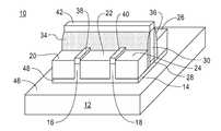
- FIG. 1is a three dimensional view of one embodiment of the invention showing a completed FinFET 10 .
- FinFET 10comprises a substrate 12 , a semiconductor structure 14 , fins 16 and 18 , epitaxial SiGe layers 20 , 22 , 24 and 26 , gate dielectric 28 , gate conductor 30 , spacers 34 and 36 , and metal silicide regions 38 , 40 and 42 .
- Substrate 12has an upper surface 46 and may be an insulator such as a buried oxide in a Silicon-on-Insulator (SOI) wafer (shown in part).
- SOISilicon-on-Insulator
- a silicon substrate(not shown) would be underneath insulating substrate 12 and a silicon layer would be above insulating substrate 12 .
- semiconductor structure 14which may be formed from a silicon layer (shown in part) above insulating substrate 12 .
- the thickness of the silicon layershould be at least the height of Si fins 16 and 18 above upper surface 46 and may be formed by reactive ion etching (RIE) a pattern for fins into the silicon layer.
- RIEreactive ion etching
- Semiconductor structure 14is comprised of single crystal Si containing material and comprises lateral Si containing layer 48 and fins 16 and 18 extending upward from the lateral Si containing layer as one solid structure.
- Gate dielectric 28may be a high K dielectric constant material.
- Gate conductor 30may be patterned polysilicon. Spacers 34 and 36 are formed on sidewalls of gate dielectric 28 , gate conductor 30 and cap layer 70 shown in FIGS. 3 and 4 and are of insulating material.
- Epitaxial SiGe layers 20 , 22 , 24 and 26are epitaxial grown on lateral Si containing layer 48 and on the sidewalls of fins 16 and 18 .
- SiGe layers 20 , 22 , 24 and 26have strain on both sidewalls and planar surfaces to increase carrier mobility in the channel of FinFET 10 .
- Metal silicide regions 38 , 40 and 42are formed such as by a self aligned process for making electrical contact to each fin 16 and 18 at the source and drain on each fin and to gate conductor 30 .
- FIG. 2is a three dimensional view of a semiconductor structure 54 during initial processing to form FinFET 10 .
- Si fins 16 and 18may be formed by REI with protective oxide caps 56 and 58 forming a mask through which the fins 16 and 18 were protected and formed during etching.
- Fins 16 and 18may have a height in the range from 5 nm to 100 nm, preferably from 15 nm to 30 nm and a width in the range from 5 nm to 500 nm and preferably 10-50 nm.
- sidewalls 60 , 61 , 62 and 63 of fins 16 and 18respectively are smooth and flat forming a fin of uniform thickness.
- Sidewalls 60 and 61 of fin 16 and sidewalls 62 and 63 of fin 18can have any crystalline surface such as ⁇ 100 ⁇ , ⁇ 110 ⁇ , ⁇ 111 ⁇ , ⁇ 311 ⁇ , ⁇ 211 ⁇ , etc.
- sidewalls 60 - 63have (100) surface for nFETs AND (110) FOR pFETs.
- Lateral Si containing layer 48has upper surface regions 64 , 66 and 68 which are smooth and flat forming a lateral Si layer of uniform thickness.
- a smooth surfaceis one that has a Root Mean Square (RMS) roughness of less than 1 nm.
- Surface regions 64 , 66 and 68can have any crystalline surface.
- RMSRoot Mean Square
- surface regions 64 , 66 and 68have ⁇ 100 ⁇ or ⁇ 110 ⁇ crystalline surface.
- the perimeter of lateral Si containing layer 48may be determined by a separate etch step through a mask to etch away lateral Si containing layer 48 to upper surface 46 of substrate 12 .
- FIG. 3is a three dimensional view of a semiconductor structure 69 including a gate dielectric 28 , gate conductor 30 and cap layer 70 on gate conductor 30 .
- Gate dielectric 28is first deposited over surface regions 64 , 66 , and 68 , and sidewalls 60 , 61 , 62 and 63 of fins 16 and 18 .
- Gate dielectric 28may comprise silicon oxide, silicon nitride, silicon oxynitride, high-k materials, or any combination of these materials.
- high-k materialsinclude but are not limited to metal oxides such as hafnium oxide, hafnium silicon oxide, hafnium silicon oxynitride, lanthanum oxide, lanthanum aluminum oxide, zirconium oxide, zirconium silicon oxide, zirconium silicon oxynitride, tantalum oxide, titanium oxide, barium strontium titanium oxide, barium titanium oxide, strontium titanium oxide, yttrium oxide, aluminum oxide, lead scandium tantalum oxide, and lead zinc niobate.
- the high-k materialsmay further include dopants such as lanthanum or aluminum.
- Gate conductor 30is then formed over gate dielectric 28 .
- the channel of FinFET 10is below gate conductor 30 between the source and drain.
- Gate conductor 30is planarized above the highest position of gate dielectric 28 such as where the gate dielectric passes over oxide caps 56 and 58 on fins 16 and 18 , respectively.
- a cap layer 70is formed on gate conductor 30 which may be, for example, silicon nitride. The cap layer 70 , gate conductor 30 , and gate dielectric 28 are then patterned. Cap layer 70 may be first patterned and then used as a mask for subsequent etching. The thickness or width of gate conductor 30 corresponds to the width of the gate of FinFET 10 to be formed. Gate conductor 30 may have a width in the range from 5 nm to 100 nm, with 15 nm to 40 nm more typical.
- FIG. 4is a three dimensional view of a semiconductor structure 72 including spacers 76 and 78 formed on opposite sides of gate dielectric 28 , gate conductor 30 and cap layer 70 .
- Source/drain halo/extension 80is formed by ion implantation of ions into sidewalls 60 , 61 , 62 and 63 of fins 16 and 18 and upper surface regions 64 , 66 and 68 .
- Spacers 76 and 78may be formed by depositing a patterned spacer layer to cover nitride cap layer 70 and sidewalls of gate dielectric 28 , gate conductor 30 and cap layer 70 .
- Spacers 76 and 78may comprise, for example, silicon oxide, carbon doped oxide, silicon nitride, perfluorocyclobutane (PFCB), fluorosilicate glass (FSG), any stress memory dielectric materials, and low K materials where K is the dielectric constant and is less than 4.
- Spacers 76 and 78each may have a thickness at gate dielectric 28 in the range from 2 nm to 30 nm, with 4 nm to 15 nm more typical.
- ion implantation of ions into sidewalls 60 , 61 , 62 and 63 of fins 16 and 18 by using spacers 76 and 78 , cap layer 70 , oxide cap layers 56 and 58 as a maskforms the correct location of halo/extension implant 80 in upper surface regions 64 , 66 and 68 and sidewalls 60 , 61 , 62 and 63 of fins 16 and 18 .
- FIG. 5is a three dimensional view of a semiconductor structure 81 including epitaxial layers 82 , 84 , 86 and 88 comprising SiGe for a p type FinFET 10 shown in FIG. 1 .
- epitaxial layers 82 , 84 , 86 and 88may comprise, for example, Si:C.
- Sidewalls 60 , 61 , 62 and 63 of fins 16 and 18 and regions 64 , 66 and 68 shown in FIG. 4act as a seed layer for epitaxial growth.
- Sidewall 60 and region 64 shown in FIG. 4provide a seed layer for epitaxial layer 82 .
- Sidewalls 61 and 62 and region 66provide a seed layer for epitaxial layer 84 .
- Sidewall 63 and region 68provide a seed layer for epitaxial layer 86 .
- Sidewall 63 on the other side of gate conductor 30 , not shown, and region 68provide a seed layer for epitaxial layer 88 . Since regions 64 , 66 , and 68 function as seed layers for epitaxial growth, no voids are formed underneath epitaxial layers 82 , 84 , 86 and 88 .
- Spacers 76 and 78do not act as a seed layer if the spacer is an insulator.
- Epitaxial layers 82 , 84 , 86 and 88can be in-situ doped, doped by ion implantation or doped by plasma doping to dope fins 16 and 18 on either side of gate conductor 30 to form a source and drain.
- Epitaxial layers 82 , 84 , 86 and 88comprise a material having a relaxed lattice spacing different from the lattice spacing of sidewalls 60 , 61 , 62 and 63 and regions 64 , 66 and 68 to provide strain in the channel.
- the strain on sidewalls 60 , 61 , 62 and 63 and on regions 64 , 66 and 68should be tensile strain to improve mobility of hole carriers in the channel which is below gate conductor 30 between the source and drain.
- Tensile strainis obtained from SiGe which has a relaxed lattice spacing greater than Si or SiGe where Ge is less.
- Gehas a relaxed lattice spacing of about 4% greater than Si and alloys of SiGe have a relaxed lattice spacing linear or proportional to the amount of Si and Ge.
- the strain on the sidewalls 60 , 61 , 62 and 62 and regions 64 , 66 and 68should be compressive strain to improve mobility of electron carriers in the channel.
- Compressive strainis obtained from Si:C which has a lattice spacing less than Si or Si:C where C is less.
- epitaxial layers 82 , 84 , 86 and 88may have the same height as fins 16 and 18 and completely fill the space between fins 16 and 18 for optimum mobility performance.
- Epitaxial layers 82 , 84 , 86 and 88may have a height or thickness substantially the same as or greater than the height or thickness of fins 16 and 18 .
- a relaxed lattice spacingis the lattice spacing of crystalline material with no strain such as when the material is a non epitaxial layer or a layer on a non crystalline substrate.
- a strained epitaxial layeris a layer with a crystal lattice that is aligned with the crystal lattice of crystalline material having a different crystal lattice spacing. As the difference in crystal lattice spacing increases between two materials, epitaxial layers will tend to relax (become unstrained and non epitaxial) at a thinner thickness. The thickness at which a strained epitaxial layer relaxes due to the difference in the relaxed crystal lattice spacing of the crystalline material is known as the critical thickness.
- oxide caps 56 and 58are removed from fins 16 and 18 up to spacers 76 and 78 .
- Nitride cap 70is removed from gate conductor 30 .
- a metalmay be formed over exposed fins 16 and 18 and gate conductor 30 and heated to react the metal with Si to form a metal silicide such as Ni silicide. Unreacted metal is removed via a selective etch.
- the metal silicide on fins 16 and 18provide contact conductors for making electrical contact to each fin.
- the fins on one side of gate conductor 30forms contacts to the source of FinFET 10 shown in FIG. 1 and the fins on the other side of gate conductor 30 forms the contacts to the drain of FinFET 10 .
- the metal silicide on gate conductor 30provides a contact conductor for making electrical contact to the gate of FinFET 10 .
- FIG. 6is a three dimensional view of an alternate embodiment of the invention where the FinFET may be a trigate.
- a semiconductor structure 90 including a gate dielectric 28 , gate conductor 30 and cap layer 70 on gate conductor 30is shown.
- Gate dielectric 28is formed over surface regions 64 , 66 , and 68 , sidewalls 60 , 61 , 62 and 63 and upper surfaces 92 and 94 of fins 16 and 18 .
- Gate conductor 30is formed over gate dielectric 28 to form a trigate FinFET on fins 16 and 18 .
- Trigate FinFET 96is formed by sidewall 60 , upper surface 92 and sidewall 61 below gate dielectric 28 and gate conductor 30 .
- Trigate FinFET 98is formed by sidewall 62 , upper surface 94 and sidewall 63 below gate dielectric 28 and gate conductor 30 .
- Trigate FinFETs 96 and 98may be completed as described with reference to FIGS. 4 and 5 except upper surfaces 92 and 94 may be implanted with ions to form halo/extension 80 for the FETs on upper surfaces 92 and 94 .
- Gate conductor 30is planarized above the highest position of gate dielectric 28 such as where the gate dielectric passes over upper surfaces 92 and 94 of fins 16 and 18 , respectively.
- a cap layer 70is formed on gate conductor 30 which may be, for example, silicon nitride. The cap layer 70 , gate conductor 30 , and gate dielectric 28 are then patterned. Cap layer 70 may be first patterned and then used as a mask for subsequent etching. The thickness or width of gate conductor 30 corresponds to the width of the trigate of FinFETs 96 and 98 . Gate conductor 30 may have a width in the range from 5 nm to 100 nm, with 15 nm to 40 nm more typical.
- FIGS. 1-6like references are used for functions corresponding to the apparatus of an earlier Figure.
Landscapes
- Thin Film Transistor (AREA)
Abstract
Description
- The present invention relates to a MOSFET and more specifically, to a FINFET having at least two fins.
- FinFET devices are becoming a viable approach for continued CMOS scaling such as beyond 32 nm. Forming a strained FinFET, e.g., by embedded SiGe/Si:C in source/drain regions, however, turns out to be very challenging. Prior art FinFET structures, before source/drain epitaxial growth, have a thin fin with flat sidewalls and may have an insulating cap. The fins are formed on a buried oxide layer. After source/drain epitaxial growth on the fin sidewalls, the fin sidewalls have a facet profile extending out from the fin sidewall, leaving a void underneath the facet.
- A field effect transistor comprising an insulating substrate having an upper surface, a single crystalline silicon containing structure on the upper surface of the substrate, the structure having first regions of substantially the same thickness and at least two spaced apart fins extending upward from the first regions, the fins having sidewalls and an upper surface, a gate dielectric on a plurality of the first regions and on the sidewalls of the at least two fins, a gate conductor on the gate dielectric on the plurality of the first regions and on the sidewalls of the at least two fins, first and second insulating spacers adjacent first and second sidewalls of the gate conductor, an epitaxial layer of a silicon containing material having a relaxed lattice spacing different from the lattice spacing of the first regions and sidewalls, the epitaxial layer extending from the sidewalls of the fins and portions of the first regions whereby the epitaxial layer imparts strain to the portions of the first regions and sidewalls of at least two fins, and contact conductors for making electrical contact to a fin, on each side of the gate conductor to make a source and drain contact, respectively, and to the gate conductor.
- These and other features, objects, and advantages of the present invention will become apparent upon consideration of the following detailed description of the invention when read in conjunction with the drawing in which:
FIG. 1 is a three dimensional view of one embodiment of the invention showing a FinFET.FIG. 2 is a three dimensional view of a semiconductor structure including fins.FIG. 3 is a three dimensional view of a semiconductor structure including a gate dielectric, gate conductor and cap layer.FIG. 4 is a three dimensional view of a semiconductor structure including a sidewall spacer on opposite sides of the gate dielectric, gate conductor and cap layer.FIG. 5 is a three dimensional view of a semiconductor structure including an epitaxial SiGe layer in the source and drain regions.FIG. 6 is a three dimensional view of an alternate embodiment of the invention showing a trigate FinFET.- Referring now to the drawing, the process for forming a fin field effect transistor (FinFET) having at least two fins and an epitaxial strain layer on the source and drain is illustrated.
FIG. 1 is a three dimensional view of one embodiment of the invention showing a completed FinFET10. FinFET10 comprises asubstrate 12, asemiconductor structure 14,fins epitaxial SiGe layers gate conductor 30,spacers metal silicide regions Substrate 12 has anupper surface 46 and may be an insulator such as a buried oxide in a Silicon-on-Insulator (SOI) wafer (shown in part). In an SOI wafer, a silicon substrate (not shown) would be underneathinsulating substrate 12 and a silicon layer would be above insulatingsubstrate 12. Aboveinsulating substrate 12 issemiconductor structure 14 which may be formed from a silicon layer (shown in part) aboveinsulating substrate 12. The thickness of the silicon layer should be at least the height ofSi fins upper surface 46 and may be formed by reactive ion etching (RIE) a pattern for fins into the silicon layer. The RIE is terminated before etching completely through the Si layer to leavefins Si containing layer 48 shown inFIG. 1 .Semiconductor structure 14 is comprised of single crystal Si containing material and comprises lateralSi containing layer 48 andfins Gate conductor 30 may be patterned polysilicon.Spacers gate conductor 30 andcap layer 70 shown inFIGS. 3 and 4 and are of insulating material. Epitaxial SiGe layers20,22,24 and26 are epitaxial grown on lateralSi containing layer 48 and on the sidewalls offins FinFET 10.Metal silicide regions fin gate conductor 30.FIG. 2 is a three dimensional view of asemiconductor structure 54 during initial processing to formFinFET 10.Si fins fins Fins FIG. 2 , sidewalls60,61,62 and63 offins fin 16 andsidewalls fin 18 can have any crystalline surface such as {100}, {110}, {111}, {311}, {211}, etc. Preferably, sidewalls60-63 have (100) surface for nFETs AND (110) FOR pFETs. LateralSi containing layer 48 hasupper surface regions Surface regions surface regions Si containing layer 48 may be determined by a separate etch step through a mask to etch away lateralSi containing layer 48 toupper surface 46 ofsubstrate 12.FIG. 3 is a three dimensional view of asemiconductor structure 69 including agate dielectric 28,gate conductor 30 andcap layer 70 ongate conductor 30.Gate dielectric 28 is first deposited oversurface regions fins Gate dielectric 28 may comprise silicon oxide, silicon nitride, silicon oxynitride, high-k materials, or any combination of these materials. Examples of high-k materials include but are not limited to metal oxides such as hafnium oxide, hafnium silicon oxide, hafnium silicon oxynitride, lanthanum oxide, lanthanum aluminum oxide, zirconium oxide, zirconium silicon oxide, zirconium silicon oxynitride, tantalum oxide, titanium oxide, barium strontium titanium oxide, barium titanium oxide, strontium titanium oxide, yttrium oxide, aluminum oxide, lead scandium tantalum oxide, and lead zinc niobate. The high-k materials may further include dopants such as lanthanum or aluminum.Gate conductor 30 is then formed overgate dielectric 28. The channel ofFinFET 10 is belowgate conductor 30 between the source and drain.Gate conductor 30 is planarized above the highest position of gate dielectric28 such as where the gate dielectric passes over oxide caps56 and58 onfins cap layer 70 is formed ongate conductor 30 which may be, for example, silicon nitride. Thecap layer 70,gate conductor 30, andgate dielectric 28 are then patterned.Cap layer 70 may be first patterned and then used as a mask for subsequent etching. The thickness or width ofgate conductor 30 corresponds to the width of the gate ofFinFET 10 to be formed.Gate conductor 30 may have a width in the range from 5 nm to 100 nm, with 15 nm to 40 nm more typical.FIG. 4 is a three dimensional view of asemiconductor structure 72 includingspacers gate dielectric 28,gate conductor 30 andcap layer 70. Source/drain halo/extension 80 is formed by ion implantation of ions intosidewalls fins upper surface regions Spacers nitride cap layer 70 and sidewalls ofgate dielectric 28,gate conductor 30 andcap layer 70. A RIE step removes the spacer layer on horizontal surfaces and shapes spacers76 and78 on vertical surfaces to be narrow at the top and thicker at the bottom.Spacers Spacers - Optionally, ion implantation of ions into
sidewalls fins spacers cap layer 70, oxide cap layers56 and58 as a mask forms the correct location of halo/extension implant 80 inupper surface regions fins FIG. 5 is a three dimensional view of asemiconductor structure 81 includingepitaxial layers a p type FinFET 10 shown inFIG. 1 . For ann type FinFET 10, epitaxial layers82,84,86 and88 may comprise, for example, Si:C. Sidewalls fins regions FIG. 4 act as a seed layer for epitaxial growth.Sidewall 60 andregion 64 shown inFIG. 4 provide a seed layer forepitaxial layer 82. Sidewalls61 and62 andregion 66 provide a seed layer forepitaxial layer 84.Sidewall 63 andregion 68 provide a seed layer forepitaxial layer 86.Sidewall 63 on the other side ofgate conductor 30, not shown, andregion 68 provide a seed layer forepitaxial layer 88. Sinceregions epitaxial layers Spacers - Epitaxial layers82,84,86 and88 can be in-situ doped, doped by ion implantation or doped by plasma doping to
dope fins gate conductor 30 to form a source and drain. Epitaxial layers82,84,86 and88 comprise a material having a relaxed lattice spacing different from the lattice spacing ofsidewalls regions sidewalls regions gate conductor 30 between the source and drain. Tensile strain is obtained from SiGe which has a relaxed lattice spacing greater than Si or SiGe where Ge is less. Ge has a relaxed lattice spacing of about 4% greater than Si and alloys of SiGe have a relaxed lattice spacing linear or proportional to the amount of Si and Ge. For n type FinFETs, the strain on thesidewalls regions FIG. 5 , epitaxial layers82,84,86 and88 may have the same height asfins fins fins - A relaxed lattice spacing is the lattice spacing of crystalline material with no strain such as when the material is a non epitaxial layer or a layer on a non crystalline substrate. A strained epitaxial layer is a layer with a crystal lattice that is aligned with the crystal lattice of crystalline material having a different crystal lattice spacing. As the difference in crystal lattice spacing increases between two materials, epitaxial layers will tend to relax (become unstrained and non epitaxial) at a thinner thickness. The thickness at which a strained epitaxial layer relaxes due to the difference in the relaxed crystal lattice spacing of the crystalline material is known as the critical thickness.
- Next, oxide caps56 and58 are removed from
fins spacers Nitride cap 70 is removed fromgate conductor 30. A metal may be formed over exposedfins gate conductor 30 and heated to react the metal with Si to form a metal silicide such as Ni silicide. Unreacted metal is removed via a selective etch. The metal silicide onfins gate conductor 30 forms contacts to the source ofFinFET 10 shown inFIG. 1 and the fins on the other side ofgate conductor 30 forms the contacts to the drain ofFinFET 10. The metal silicide ongate conductor 30 provides a contact conductor for making electrical contact to the gate ofFinFET 10. FIG. 6 is a three dimensional view of an alternate embodiment of the invention where the FinFET may be a trigate. InFIG. 6 , asemiconductor structure 90 including agate dielectric 28,gate conductor 30 andcap layer 70 ongate conductor 30 is shown.Gate dielectric 28 is formed oversurface regions upper surfaces fins Gate conductor 30 is formed over gate dielectric28 to form a trigate FinFET onfins Trigate FinFET 96 is formed bysidewall 60,upper surface 92 andsidewall 61 belowgate dielectric 28 andgate conductor 30.Trigate FinFET 98 is formed bysidewall 62,upper surface 94 andsidewall 63 belowgate dielectric 28 andgate conductor 30.Trigate FinFETs FIGS. 4 and 5 exceptupper surfaces extension 80 for the FETs onupper surfaces Gate conductor 30 is planarized above the highest position of gate dielectric28 such as where the gate dielectric passes overupper surfaces fins cap layer 70 is formed ongate conductor 30 which may be, for example, silicon nitride. Thecap layer 70,gate conductor 30, andgate dielectric 28 are then patterned.Cap layer 70 may be first patterned and then used as a mask for subsequent etching. The thickness or width ofgate conductor 30 corresponds to the width of the trigate ofFinFETs Gate conductor 30 may have a width in the range from 5 nm to 100 nm, with 15 nm to 40 nm more typical.- In
FIGS. 1-6 , like references are used for functions corresponding to the apparatus of an earlier Figure. - While there has been described and illustrated a FinFET comprising at least two spaced apart fins and epitaxial layers of a different relaxed lattice spacing grown on the fins and semiconductor regions between the fins to impart strain to increase carrier mobility, it will be apparent to those skilled in the art that modifications and variations are possible without deviating from the broad scope of the invention which shall be limited solely by the scope of the claims appended hereto.
Claims (22)
1. A field effect transistor comprising:
an insulating substrate having an upper surface,
a single crystalline silicon containing structure on said upper surface of said substrate,
said structure having first regions of substantially the same thickness and at least two spaced apart fins extending upward from said first regions,
said fins having sidewalls and an upper surface,
a gate dielectric on a plurality of said first regions and on said sidewalls of said at least two fins,
a gate conductor on said gate dielectric on said plurality of said first regions and on said sidewalls of said at least two fins,
first and second insulating spacers adjacent first and second sidewalls of said gate conductor,
an epitaxial layer of a silicon containing material having a relaxed lattice spacing different from the lattice spacing of said first regions and sidewalls, said epitaxial layer extending from said sidewalls of said fins and portions of said first regions whereby said epitaxial layer imparts strain to said portions of said first regions and sidewalls of at least two fins, and
contact conductors for making electrical contact to a fin on each side of said gate conductor to make a source and drain contact, respectively, and to said gate conductor.
2. The field effect transistor ofclaim 1 wherein said gate conductor has a width in the range from 5 nm to 100 nm.
3. The field effect transistor ofclaim 1 wherein said gate dielectric and gate conductor have a height higher than said at least two fins.
4. The field effect transistor ofclaim 1 wherein said epitaxial layer is selected from the group consisting of SiGe and Si:C.
5. The field effect transistor ofclaim 1 wherein one of said first regions extends between two of said at least two fins and wherein a portion of said epitaxial layer extends between said two fins and extends from said one of said first regions.
6. The field effect transistor ofclaim 1 wherein said one of said first regions is adjacent said first insulating spacer.
7. The field effect transistor ofclaim 1 wherein said epitaxial layer extends from each sidewall of said at least two fins on both sides of said gate conductor.
8. The field effect transistor ofclaim 1 wherein said at least two fins and said first regions are Si.
9. The field effect transistor ofclaim 1 wherein said contact conductors include metal silicide.
10. The field effect transistor ofclaim 1 wherein said gate conductor includes polysilicon.
11. The field effect transistor ofclaim 1 wherein said gate dielectric is on said upper surface of at least two of said fins and wherein said gate conductor is on said gate dielectric on said upper surface of at least two of said fins to form two trigate FinFETs.
12. A method for forming a field effect transistor comprising:
selecting a layer of single crystal silicon containing semiconductor material on an insulating substrate,
forming in said layer first regions of substantially the same thickness and at least two spaced apart fins extending upward from said first regions,
said fins having sidewalls and an upper surface,
forming a gate dielectric on a plurality of said first regions and on said sidewalls,
forming a gate conductor on said gate dielectric on said plurality of said first regions and on said sidewalls of said at least two fins,
forming first and second insulating spacers adjacent first and second sidewalls of said gate conductor,
forming an epitaxial layer of a silicon containing material having a relaxed lattice spacing different from the lattice spacing of said first regions and sidewalls, said epitaxial layer extending from said sidewalls of said fins and portions of said first regions whereby said epitaxial layer imparts strain to said portions of said first regions and sidewalls of at least two fins, and
forming contact conductors for making electrical contact to a fin on each side of said gate conductor to make a source and drain contact, respectively, and to said gate conductor to make a gate contact.
13. The method ofclaim 12 wherein gate conductor has a width in the range from 5 nm to 100 nm.
14. The method ofclaim 12 wherein said gate dielectric and gate conductor are formed to a height higher than said at least two fins.
15. The method ofclaim 12 wherein said epitaxial layer is selected from the group consisting of SiGe and Si:C.
16. The method ofclaim 12 wherein one of said first regions are formed to extend between two of said at least two fins and wherein a portion of said epitaxial layer is formed to extend between said two fins and extends from said one of said first regions.
17. The method ofclaim 12 wherein said one of said first regions is formed adjacent said first insulating spacer.
18. The method ofclaim 12 wherein said epitaxial layer extends from each sidewall of said at least two fins on both sides of said gate conductor.
19. The method ofclaim 12 wherein said at least two fins and said first regions are Si.
20. The method ofclaim 12 wherein said forming contact conductors include forming metal silicide.
21. The method ofclaim 12 wherein said gate conductor includes polysilicon.
22. The method ofclaim 12 further including forming a gate dielectric on said upper surface of at least two of said fins and forming a gate conductor on said gate dielectric on said upper surface of at least two of said fins to form two trigate FinFETs.
Priority Applications (1)
| Application Number | Priority Date | Filing Date | Title |
|---|---|---|---|
| US12/787,383US20110291188A1 (en) | 2010-05-25 | 2010-05-25 | Strained finfet |
Applications Claiming Priority (1)
| Application Number | Priority Date | Filing Date | Title |
|---|---|---|---|
| US12/787,383US20110291188A1 (en) | 2010-05-25 | 2010-05-25 | Strained finfet |
Publications (1)
| Publication Number | Publication Date |
|---|---|
| US20110291188A1true US20110291188A1 (en) | 2011-12-01 |
Family
ID=45021375
Family Applications (1)
| Application Number | Title | Priority Date | Filing Date |
|---|---|---|---|
| US12/787,383AbandonedUS20110291188A1 (en) | 2010-05-25 | 2010-05-25 | Strained finfet |
Country Status (1)
| Country | Link |
|---|---|
| US (1) | US20110291188A1 (en) |
Cited By (45)
| Publication number | Priority date | Publication date | Assignee | Title |
|---|---|---|---|---|
| US8445334B1 (en)* | 2011-12-20 | 2013-05-21 | International Business Machines Corporation | SOI FinFET with recessed merged Fins and liner for enhanced stress coupling |
| WO2013089953A1 (en)* | 2011-12-16 | 2013-06-20 | International Business Machines Corporation | Rare-earth oxide isolated semiconductor fin |
| US8796093B1 (en)* | 2013-03-14 | 2014-08-05 | International Business Machines Corporation | Doping of FinFET structures |
| CN103985754A (en)* | 2013-02-08 | 2014-08-13 | 中国科学院微电子研究所 | Semiconductor device and method for manufacturing the same |
| CN103985752A (en)* | 2013-02-08 | 2014-08-13 | 中国科学院微电子研究所 | Semiconductor arrangement and method for the production thereof |
| WO2014121545A1 (en)* | 2013-02-08 | 2014-08-14 | 中国科学院微电子研究所 | Semiconductor device and manufacturing method thereof |
| CN104051272A (en)* | 2013-03-15 | 2014-09-17 | 国际商业机器公司 | Stress Enhanced FINFET Devices |
| KR20140113257A (en)* | 2013-03-14 | 2014-09-24 | 삼성전자주식회사 | Semiconductor device and method for fabricating the same |
| US8871626B2 (en) | 2011-12-20 | 2014-10-28 | International Business Machines Corporation | FinFET with vertical silicide structure |
| CN104246994A (en)* | 2012-04-17 | 2014-12-24 | 国际商业机器公司 | Semiconductor device with fin structure and method of forming semiconductor device with fin structure |
| US20140374827A1 (en)* | 2013-06-24 | 2014-12-25 | Samsung Electronics Co., Ltd. | Semiconductor device and method for fabricating the same |
| US20150064892A1 (en)* | 2013-08-29 | 2015-03-05 | International Business Machines Corporation | Semiconductor devices and methods of manufacture |
| US20150145064A1 (en)* | 2013-11-22 | 2015-05-28 | International Business Machines Corporation | FinFET HAVING SUPPRESSED LEAKAGE CURRENT |
| US20150187915A1 (en)* | 2013-12-26 | 2015-07-02 | Samsung Electronics Co., Ltd. | Method for fabricating fin type transistor |
| US9087900B1 (en) | 2014-01-07 | 2015-07-21 | Samsung Electronics Co., Ltd. | Semiconductor device and method for fabricating the same |
| US9105663B1 (en) | 2014-01-30 | 2015-08-11 | International Business Machines Corporation | FinFET with silicon germanium stressor and method of forming |
| US20150228789A1 (en)* | 2014-02-12 | 2015-08-13 | Kabushiki Kaisha Toshiba | Stressed channel bulk fin field effect transistor |
| US20150228755A1 (en)* | 2014-02-11 | 2015-08-13 | GlobalFoundries, Inc. | Integrated circuits with relaxed silicon / germanium fins |
| US20150228654A1 (en)* | 2013-03-21 | 2015-08-13 | International Business Machines Corporation | Method and structure for finfet cmos |
| US20150255457A1 (en)* | 2014-03-04 | 2015-09-10 | International Business Machines Corporation | Methods and apparatus to form fin structures of different compositions on a same wafer via mandrel and diffusion |
| US20150270365A1 (en)* | 2014-03-20 | 2015-09-24 | International Business Machines Corporation | Selective dielectric spacer deposition for exposing sidewalls of a finfet |
| US20150295021A1 (en)* | 2011-07-25 | 2015-10-15 | Synopsys, Inc. | Integrated circuit devices having features with reduced edge curvature and methods for manufacturing the same |
| US9196479B1 (en)* | 2014-07-03 | 2015-11-24 | International Business Machines Corporation | Method of co-integration of strained silicon and strained germanium in semiconductor devices including fin structures |
| US20150371867A1 (en)* | 2014-06-24 | 2015-12-24 | International Business Machines Corporation | Protective trench layer and gate spacer in finfet devices |
| US20160049515A1 (en)* | 2013-12-27 | 2016-02-18 | International Business Machines Corporation | Finfet including improved epitaxial topology |
| US9324850B2 (en) | 2013-02-26 | 2016-04-26 | Samsung Electronics Co., Ltd. | Integrated circuit devices and fabricating method thereof |
| US9391171B2 (en) | 2014-01-24 | 2016-07-12 | International Business Machines Corporation | Fin field effect transistor including a strained epitaxial semiconductor shell |
| US9484201B2 (en) | 2015-02-23 | 2016-11-01 | International Business Machines Corporation | Epitaxial silicon germanium fin formation using sacrificial silicon fin templates |
| US9493678B2 (en) | 2014-11-10 | 2016-11-15 | Uwiz Technology Co., Ltd. | Polishing composition |
| TWI565057B (en)* | 2013-12-19 | 2017-01-01 | 英特爾股份有限公司 | Self-aligned gate edge and local interconnect structure and method of fabricating the same |
| US9536881B2 (en) | 2013-04-23 | 2017-01-03 | Samsung Electronics Co., Ltd. | Semiconductor devices having fin shaped channels |
| US20170033284A1 (en)* | 2015-04-16 | 2017-02-02 | Stmicroelectronics, Inc. | High density resistive random access memory (rram) |
| US9583486B1 (en) | 2015-11-19 | 2017-02-28 | International Business Machines Corporation | Stable work function for narrow-pitch devices |
| US20170077306A1 (en)* | 2014-12-31 | 2017-03-16 | Stmicroelectronics, Inc. | Vertical slit transistor with optimized ac performance |
| US9601385B1 (en)* | 2016-01-27 | 2017-03-21 | International Business Machines Corporation | Method of making a dual strained channel semiconductor device |
| US9660080B2 (en) | 2014-02-28 | 2017-05-23 | Stmicroelectronics, Inc. | Multi-layer strained channel FinFET |
| US9768299B2 (en) | 2014-02-21 | 2017-09-19 | Stmicroelectronics Inc. | Method to form strained channel in thin box SOI structures by elastic strain relaxation of the substrate |
| US20170309628A1 (en)* | 2016-02-26 | 2017-10-26 | Globalfoundries Inc. | Finfet device with enlarged channel regions |
| US9818877B2 (en) | 2014-09-18 | 2017-11-14 | International Business Machines Corporation | Embedded source/drain structure for tall finFET and method of formation |
| US9893171B2 (en) | 2016-06-03 | 2018-02-13 | International Business Machines Corporation | Fin field effect transistor fabrication and devices having inverted T-shaped gate |
| US20180069131A1 (en)* | 2016-09-02 | 2018-03-08 | International Business Machines Corporation | Stacked series connected vfets for high voltage applications |
| US10032859B2 (en) | 2011-09-08 | 2018-07-24 | Synopsys, Inc. | Methods for manufacturing integrated circuit devices having features with reduced edge curvature |
| US10559690B2 (en) | 2014-09-18 | 2020-02-11 | International Business Machines Corporation | Embedded source/drain structure for tall FinFET and method of formation |
| US11139402B2 (en) | 2018-05-14 | 2021-10-05 | Synopsys, Inc. | Crystal orientation engineering to achieve consistent nanowire shapes |
| US11264458B2 (en) | 2019-05-20 | 2022-03-01 | Synopsys, Inc. | Crystal orientation engineering to achieve consistent nanowire shapes |
Citations (15)
| Publication number | Priority date | Publication date | Assignee | Title |
|---|---|---|---|---|
| US6562665B1 (en)* | 2000-10-16 | 2003-05-13 | Advanced Micro Devices, Inc. | Fabrication of a field effect transistor with a recess in a semiconductor pillar in SOI technology |
| US7071064B2 (en)* | 2004-09-23 | 2006-07-04 | Intel Corporation | U-gate transistors and methods of fabrication |
| US7271456B2 (en)* | 2004-07-27 | 2007-09-18 | Samsung Electronics Co., Ltd. | Semiconductor devices including stress inducing layers |
| US20070221956A1 (en)* | 2006-03-23 | 2007-09-27 | Kabushiki Kaisha Toshiba | Semiconductor device and method of fabricating the same |
| US20070262353A1 (en)* | 2006-04-28 | 2007-11-15 | Nobuyasu Nishiyama | Semiconductor device and method of fabricating the same |
| US7314787B2 (en)* | 2004-03-10 | 2008-01-01 | Kabushiki Kaisha Toshiba | Method of manufacturing a semiconductor device |
| US7388258B2 (en)* | 2003-12-10 | 2008-06-17 | International Business Machines Corporation | Sectional field effect devices |
| US7393733B2 (en)* | 2004-12-01 | 2008-07-01 | Amberwave Systems Corporation | Methods of forming hybrid fin field-effect transistor structures |
| US7419857B2 (en)* | 2005-12-20 | 2008-09-02 | Korea Advanced Institute Of Science And Technology | Method for manufacturing field effect transistor having channel consisting of silicon fins and silicon body and transistor structure manufactured thereby |
| US7452768B2 (en)* | 2005-10-25 | 2008-11-18 | Freescale Semiconductor, Inc. | Multiple device types including an inverted-T channel transistor and method therefor |
| US7470951B2 (en)* | 2005-01-31 | 2008-12-30 | Freescale Semiconductor, Inc. | Hybrid-FET and its application as SRAM |
| US7473967B2 (en)* | 2003-05-30 | 2009-01-06 | Panasonic Corporation | Strained channel finFET device |
| US7692254B2 (en)* | 2007-07-16 | 2010-04-06 | International Business Machines Corporation | Fin-type field effect transistor structure with merged source/drain silicide and method of forming the structure |
| US7977174B2 (en)* | 2009-06-08 | 2011-07-12 | Globalfoundries Inc. | FinFET structures with stress-inducing source/drain-forming spacers and methods for fabricating the same |
| US8153493B2 (en)* | 2008-08-28 | 2012-04-10 | Taiwan Semiconductor Manufacturing Company, Ltd. | FinFET process compatible native transistor |
- 2010
- 2010-05-25USUS12/787,383patent/US20110291188A1/ennot_activeAbandoned
Patent Citations (15)
| Publication number | Priority date | Publication date | Assignee | Title |
|---|---|---|---|---|
| US6562665B1 (en)* | 2000-10-16 | 2003-05-13 | Advanced Micro Devices, Inc. | Fabrication of a field effect transistor with a recess in a semiconductor pillar in SOI technology |
| US7473967B2 (en)* | 2003-05-30 | 2009-01-06 | Panasonic Corporation | Strained channel finFET device |
| US7388258B2 (en)* | 2003-12-10 | 2008-06-17 | International Business Machines Corporation | Sectional field effect devices |
| US7314787B2 (en)* | 2004-03-10 | 2008-01-01 | Kabushiki Kaisha Toshiba | Method of manufacturing a semiconductor device |
| US7271456B2 (en)* | 2004-07-27 | 2007-09-18 | Samsung Electronics Co., Ltd. | Semiconductor devices including stress inducing layers |
| US7071064B2 (en)* | 2004-09-23 | 2006-07-04 | Intel Corporation | U-gate transistors and methods of fabrication |
| US7393733B2 (en)* | 2004-12-01 | 2008-07-01 | Amberwave Systems Corporation | Methods of forming hybrid fin field-effect transistor structures |
| US7470951B2 (en)* | 2005-01-31 | 2008-12-30 | Freescale Semiconductor, Inc. | Hybrid-FET and its application as SRAM |
| US7452768B2 (en)* | 2005-10-25 | 2008-11-18 | Freescale Semiconductor, Inc. | Multiple device types including an inverted-T channel transistor and method therefor |
| US7419857B2 (en)* | 2005-12-20 | 2008-09-02 | Korea Advanced Institute Of Science And Technology | Method for manufacturing field effect transistor having channel consisting of silicon fins and silicon body and transistor structure manufactured thereby |
| US20070221956A1 (en)* | 2006-03-23 | 2007-09-27 | Kabushiki Kaisha Toshiba | Semiconductor device and method of fabricating the same |
| US20070262353A1 (en)* | 2006-04-28 | 2007-11-15 | Nobuyasu Nishiyama | Semiconductor device and method of fabricating the same |
| US7692254B2 (en)* | 2007-07-16 | 2010-04-06 | International Business Machines Corporation | Fin-type field effect transistor structure with merged source/drain silicide and method of forming the structure |
| US8153493B2 (en)* | 2008-08-28 | 2012-04-10 | Taiwan Semiconductor Manufacturing Company, Ltd. | FinFET process compatible native transistor |
| US7977174B2 (en)* | 2009-06-08 | 2011-07-12 | Globalfoundries Inc. | FinFET structures with stress-inducing source/drain-forming spacers and methods for fabricating the same |
Cited By (93)
| Publication number | Priority date | Publication date | Assignee | Title |
|---|---|---|---|---|
| US9786734B2 (en)* | 2011-07-25 | 2017-10-10 | Synopsys, Inc. | Integrated circuit devices having features with reduced edge curvature and methods for manufacturing the same |
| US20150295021A1 (en)* | 2011-07-25 | 2015-10-15 | Synopsys, Inc. | Integrated circuit devices having features with reduced edge curvature and methods for manufacturing the same |
| US10256293B2 (en) | 2011-07-25 | 2019-04-09 | Synopsys, Inc. | Integrated circuit devices having features with reduced edge curvature and methods for manufacturing the same |
| US10032859B2 (en) | 2011-09-08 | 2018-07-24 | Synopsys, Inc. | Methods for manufacturing integrated circuit devices having features with reduced edge curvature |
| US9058987B2 (en) | 2011-12-16 | 2015-06-16 | International Business Machines Corporation | Rare-earth oxide isolated semiconductor fin |
| WO2013089953A1 (en)* | 2011-12-16 | 2013-06-20 | International Business Machines Corporation | Rare-earth oxide isolated semiconductor fin |
| TWI559541B (en)* | 2011-12-16 | 2016-11-21 | 萬國商業機器公司 | Rare earth oxide isolated semiconductor fin |
| JP2015508567A (en)* | 2011-12-16 | 2015-03-19 | インターナショナル・ビジネス・マシーンズ・コーポレーションInternational Business Machines Corporation | Semiconductor structure and manufacturing method thereof (rare earth oxide separation type semiconductor fin) |
| GB2510525A (en)* | 2011-12-16 | 2014-08-06 | Ibm | Rare-earth oxide isolated semiconductor fin |
| GB2510525B (en)* | 2011-12-16 | 2015-12-16 | Ibm | Rare-earth oxide isolated semiconductor fin |
| US8853781B2 (en) | 2011-12-16 | 2014-10-07 | International Business Machines Corporation | Rare-earth oxide isolated semiconductor fin |
| US8871626B2 (en) | 2011-12-20 | 2014-10-28 | International Business Machines Corporation | FinFET with vertical silicide structure |
| US8445334B1 (en)* | 2011-12-20 | 2013-05-21 | International Business Machines Corporation | SOI FinFET with recessed merged Fins and liner for enhanced stress coupling |
| US8723262B2 (en) | 2011-12-20 | 2014-05-13 | International Business Machines Corporation | SOI FinFET with recessed merged fins and liner for enhanced stress coupling |
| JP2015517220A (en)* | 2012-04-17 | 2015-06-18 | インターナショナル・ビジネス・マシーンズ・コーポレーションInternational Business Machines Corporation | Semiconductor device having fin structure and method for forming semiconductor device having fin structure |
| CN104246994A (en)* | 2012-04-17 | 2014-12-24 | 国际商业机器公司 | Semiconductor device with fin structure and method of forming semiconductor device with fin structure |
| DE112013000813B4 (en) | 2012-04-17 | 2020-07-16 | Globalfoundries Inc. | Method for forming semiconductor units with fin structures |
| US10134862B2 (en) | 2013-02-08 | 2018-11-20 | Institute of Microelectronics, Chinese Academy of Sciences | Semiconductor device containing fin and back gate and method for manufacturing the same |
| WO2014121545A1 (en)* | 2013-02-08 | 2014-08-14 | 中国科学院微电子研究所 | Semiconductor device and manufacturing method thereof |
| CN103985754A (en)* | 2013-02-08 | 2014-08-13 | 中国科学院微电子研究所 | Semiconductor device and method for manufacturing the same |
| CN103985752A (en)* | 2013-02-08 | 2014-08-13 | 中国科学院微电子研究所 | Semiconductor arrangement and method for the production thereof |
| USRE49988E1 (en) | 2013-02-26 | 2024-05-28 | Samsung Electronics Co., Ltd. | Integrated circuit devices |
| US9673099B2 (en) | 2013-02-26 | 2017-06-06 | Samsung Electronics Co., Ltd. | Method of fabricating integrated circuit devices |
| US9324850B2 (en) | 2013-02-26 | 2016-04-26 | Samsung Electronics Co., Ltd. | Integrated circuit devices and fabricating method thereof |
| US8912063B2 (en) | 2013-03-14 | 2014-12-16 | Samsung Electronics Co., Ltd. | Semiconductor device having blocking pattern and method for fabricating the same |
| KR20140113257A (en)* | 2013-03-14 | 2014-09-24 | 삼성전자주식회사 | Semiconductor device and method for fabricating the same |
| US8796093B1 (en)* | 2013-03-14 | 2014-08-05 | International Business Machines Corporation | Doping of FinFET structures |
| KR102059828B1 (en)* | 2013-03-14 | 2019-12-27 | 삼성전자 주식회사 | Semiconductor device and method for fabricating the same |
| CN104051272A (en)* | 2013-03-15 | 2014-09-17 | 国际商业机器公司 | Stress Enhanced FINFET Devices |
| US20150228654A1 (en)* | 2013-03-21 | 2015-08-13 | International Business Machines Corporation | Method and structure for finfet cmos |
| US9576960B2 (en)* | 2013-03-21 | 2017-02-21 | International Business Machines Corporation | Structure for finFET CMOS |
| US9536881B2 (en) | 2013-04-23 | 2017-01-03 | Samsung Electronics Co., Ltd. | Semiconductor devices having fin shaped channels |
| US20140374827A1 (en)* | 2013-06-24 | 2014-12-25 | Samsung Electronics Co., Ltd. | Semiconductor device and method for fabricating the same |
| US20150064892A1 (en)* | 2013-08-29 | 2015-03-05 | International Business Machines Corporation | Semiconductor devices and methods of manufacture |
| US20150061017A1 (en)* | 2013-08-29 | 2015-03-05 | International Business Machines Corporation | Semiconductor devices and methods of manufacture |
| US9276115B2 (en)* | 2013-08-29 | 2016-03-01 | Globalfoundries Inc. | Semiconductor devices and methods of manufacture |
| US9299841B2 (en)* | 2013-08-29 | 2016-03-29 | Globalfoundries Inc. | Semiconductor devices and methods of manufacture |
| US20150145064A1 (en)* | 2013-11-22 | 2015-05-28 | International Business Machines Corporation | FinFET HAVING SUPPRESSED LEAKAGE CURRENT |
| US9082851B2 (en)* | 2013-11-22 | 2015-07-14 | International Business Machines Corporation | FinFET having suppressed leakage current |
| US10319812B2 (en) | 2013-12-19 | 2019-06-11 | Intel Corporation | Self-aligned gate edge and local interconnect and method to fabricate same |
| US9831306B2 (en) | 2013-12-19 | 2017-11-28 | Intel Corporation | Self-aligned gate edge and local interconnect and method to fabricate same |
| US11563081B2 (en) | 2013-12-19 | 2023-01-24 | Daedalus Prime Llc | Self-aligned gate edge and local interconnect |
| US10790354B2 (en) | 2013-12-19 | 2020-09-29 | Intel Corporation | Self-aligned gate edge and local interconnect |
| TWI565057B (en)* | 2013-12-19 | 2017-01-01 | 英特爾股份有限公司 | Self-aligned gate edge and local interconnect structure and method of fabricating the same |
| US20150187915A1 (en)* | 2013-12-26 | 2015-07-02 | Samsung Electronics Co., Ltd. | Method for fabricating fin type transistor |
| US10164110B2 (en)* | 2013-12-27 | 2018-12-25 | International Business Machines Corporation | Finfet including improved epitaxial topology |
| US20160049515A1 (en)* | 2013-12-27 | 2016-02-18 | International Business Machines Corporation | Finfet including improved epitaxial topology |
| US9087900B1 (en) | 2014-01-07 | 2015-07-21 | Samsung Electronics Co., Ltd. | Semiconductor device and method for fabricating the same |
| US9711417B2 (en) | 2014-01-24 | 2017-07-18 | International Business Machines Corporation | Fin field effect transistor including a strained epitaxial semiconductor shell |
| US9711416B2 (en) | 2014-01-24 | 2017-07-18 | International Business Machines Corporation | Fin field effect transistor including a strained epitaxial semiconductor shell |
| US9391171B2 (en) | 2014-01-24 | 2016-07-12 | International Business Machines Corporation | Fin field effect transistor including a strained epitaxial semiconductor shell |
| US9105663B1 (en) | 2014-01-30 | 2015-08-11 | International Business Machines Corporation | FinFET with silicon germanium stressor and method of forming |
| US9196710B2 (en)* | 2014-02-11 | 2015-11-24 | GlobalFoundries, Inc. | Integrated circuits with relaxed silicon / germanium fins |
| US20150228755A1 (en)* | 2014-02-11 | 2015-08-13 | GlobalFoundries, Inc. | Integrated circuits with relaxed silicon / germanium fins |
| US9484262B2 (en) | 2014-02-12 | 2016-11-01 | International Business Machines Corporation | Stressed channel bulk fin field effect transistor |
| US9246005B2 (en)* | 2014-02-12 | 2016-01-26 | International Business Machines Corporation | Stressed channel bulk fin field effect transistor |
| US20150228789A1 (en)* | 2014-02-12 | 2015-08-13 | Kabushiki Kaisha Toshiba | Stressed channel bulk fin field effect transistor |
| US9768299B2 (en) | 2014-02-21 | 2017-09-19 | Stmicroelectronics Inc. | Method to form strained channel in thin box SOI structures by elastic strain relaxation of the substrate |
| US10418488B2 (en) | 2014-02-21 | 2019-09-17 | Stmicroelectronics, Inc. | Method to form strained channel in thin box SOI structures by elastic strain relaxation of the substrate |
| US10068908B2 (en) | 2014-02-28 | 2018-09-04 | Stmicroelectronics, Inc. | Method to form localized relaxed substrate by using condensation |
| US9660081B2 (en) | 2014-02-28 | 2017-05-23 | Stmicroelectronics, Inc. | Method to form localized relaxed substrate by using condensation |
| US9660080B2 (en) | 2014-02-28 | 2017-05-23 | Stmicroelectronics, Inc. | Multi-layer strained channel FinFET |
| US9530777B2 (en)* | 2014-03-04 | 2016-12-27 | Stmicroelectronics, Inc. | FinFETs of different compositions formed on a same substrate |
| US20150255457A1 (en)* | 2014-03-04 | 2015-09-10 | International Business Machines Corporation | Methods and apparatus to form fin structures of different compositions on a same wafer via mandrel and diffusion |
| US9331166B2 (en)* | 2014-03-20 | 2016-05-03 | International Business Machines Corporation | Selective dielectric spacer deposition for exposing sidewalls of a finFET |
| US20150270365A1 (en)* | 2014-03-20 | 2015-09-24 | International Business Machines Corporation | Selective dielectric spacer deposition for exposing sidewalls of a finfet |
| US9530665B2 (en)* | 2014-06-24 | 2016-12-27 | International Business Machines Corporation | Protective trench layer and gate spacer in finFET devices |
| US20150371867A1 (en)* | 2014-06-24 | 2015-12-24 | International Business Machines Corporation | Protective trench layer and gate spacer in finfet devices |
| US9196479B1 (en)* | 2014-07-03 | 2015-11-24 | International Business Machines Corporation | Method of co-integration of strained silicon and strained germanium in semiconductor devices including fin structures |
| US10896976B2 (en) | 2014-09-18 | 2021-01-19 | International Business Machines Corporation | Embedded source/drain structure for tall FinFet and method of formation |
| US10559690B2 (en) | 2014-09-18 | 2020-02-11 | International Business Machines Corporation | Embedded source/drain structure for tall FinFET and method of formation |
| US9818877B2 (en) | 2014-09-18 | 2017-11-14 | International Business Machines Corporation | Embedded source/drain structure for tall finFET and method of formation |
| US9493678B2 (en) | 2014-11-10 | 2016-11-15 | Uwiz Technology Co., Ltd. | Polishing composition |
| US20170077306A1 (en)* | 2014-12-31 | 2017-03-16 | Stmicroelectronics, Inc. | Vertical slit transistor with optimized ac performance |
| US10134903B2 (en)* | 2014-12-31 | 2018-11-20 | Stmicroelectronics, Inc. | Vertical slit transistor with optimized AC performance |
| US9484201B2 (en) | 2015-02-23 | 2016-11-01 | International Business Machines Corporation | Epitaxial silicon germanium fin formation using sacrificial silicon fin templates |
| US9865653B2 (en)* | 2015-04-16 | 2018-01-09 | Stmicroelectronics, Inc. | High density resistive random access memory (RRAM) |
| US20170033284A1 (en)* | 2015-04-16 | 2017-02-02 | Stmicroelectronics, Inc. | High density resistive random access memory (rram) |
| US10211257B2 (en) | 2015-04-16 | 2019-02-19 | Stmicroelectronics, Inc. | High density resistive random access memory (RRAM) |
| US10170576B2 (en) | 2015-11-19 | 2019-01-01 | International Business Machines Corporation | Stable work function for narrow-pitch devices |
| US9583486B1 (en) | 2015-11-19 | 2017-02-28 | International Business Machines Corporation | Stable work function for narrow-pitch devices |
| US9735250B2 (en) | 2015-11-19 | 2017-08-15 | International Business Machines Corporation | Stable work function for narrow-pitch devices |
| US9601385B1 (en)* | 2016-01-27 | 2017-03-21 | International Business Machines Corporation | Method of making a dual strained channel semiconductor device |
| US10134730B2 (en)* | 2016-02-26 | 2018-11-20 | Globalfoundries Inc. | FinFET device with enlarged channel regions |
| US20170309628A1 (en)* | 2016-02-26 | 2017-10-26 | Globalfoundries Inc. | Finfet device with enlarged channel regions |
| US10224417B2 (en) | 2016-06-03 | 2019-03-05 | International Business Machines Corporation | Fin field effect transistor fabrication and devices having inverted T-shaped gate |
| US10319840B2 (en) | 2016-06-03 | 2019-06-11 | International Business Machines Corporation | Fin field effect transistor fabrication and devices having inverted T-shaped gate |
| US9893171B2 (en) | 2016-06-03 | 2018-02-13 | International Business Machines Corporation | Fin field effect transistor fabrication and devices having inverted T-shaped gate |
| US10784365B2 (en) | 2016-06-03 | 2020-09-22 | International Business Machines Corporation | Fin field effect transistor fabrication and devices having inverted T-shaped gate |
| US20180069131A1 (en)* | 2016-09-02 | 2018-03-08 | International Business Machines Corporation | Stacked series connected vfets for high voltage applications |
| US10580901B2 (en)* | 2016-09-02 | 2020-03-03 | International Business Machines Corporation | Stacked series connected VFETs for high voltage applications |
| US11139402B2 (en) | 2018-05-14 | 2021-10-05 | Synopsys, Inc. | Crystal orientation engineering to achieve consistent nanowire shapes |
| US11264458B2 (en) | 2019-05-20 | 2022-03-01 | Synopsys, Inc. | Crystal orientation engineering to achieve consistent nanowire shapes |
Similar Documents
| Publication | Publication Date | Title |
|---|---|---|
| US20110291188A1 (en) | Strained finfet | |
| US11257951B2 (en) | Method of making semiconductor device having first and second epitaxial materials | |
| US10388772B2 (en) | Tunneling field effect transistor (TFET) having a semiconductor fin structure | |
| US9178045B2 (en) | Integrated circuit devices including FinFETS and methods of forming the same | |
| US8030144B2 (en) | Semiconductor device with stressed fin sections, and related fabrication methods | |
| US11728400B2 (en) | Semiconductor structure | |
| US10276717B2 (en) | Channel strain inducing architecture and doping technique at replacement poly gate (RPG) stage | |
| US9728641B2 (en) | Semiconductor device and fabrication method thereof | |
| US7154118B2 (en) | Bulk non-planar transistor having strained enhanced mobility and methods of fabrication | |
| US9230828B2 (en) | Source and drain dislocation fabrication in FinFETs | |
| US10312155B2 (en) | FinFET device and fabrication method thereof | |
| US20160064288A1 (en) | DUAL CHANNEL MATERIAL FOR finFET FOR HIGH PERFORMANCE CMOS | |
| US9711417B2 (en) | Fin field effect transistor including a strained epitaxial semiconductor shell | |
| US11069809B2 (en) | Soi FinFET fins with recessed fins and epitaxy in source drain region | |
| US8563385B2 (en) | Field effect transistor device with raised active regions | |
| US20230121119A1 (en) | Method of making a semiconductor device using a dummy gate |
Legal Events
| Date | Code | Title | Description |
|---|---|---|---|
| AS | Assignment | Owner name:INTERNATIONAL BUSINESS MACHINES CORPORATION, NEW Y Free format text:ASSIGNMENT OF ASSIGNORS INTEREST;ASSIGNORS:CHENG, KANGGUO;DORIS, BRUCE B.;HUA, XUEFENG;AND OTHERS;SIGNING DATES FROM 20100510 TO 20100511;REEL/FRAME:024439/0796 | |
| STCB | Information on status: application discontinuation | Free format text:ABANDONED -- FAILURE TO RESPOND TO AN OFFICE ACTION | |
| AS | Assignment | Owner name:GLOBALFOUNDRIES U.S. 2 LLC, NEW YORK Free format text:ASSIGNMENT OF ASSIGNORS INTEREST;ASSIGNOR:INTERNATIONAL BUSINESS MACHINES CORPORATION;REEL/FRAME:036550/0001 Effective date:20150629 | |
| AS | Assignment | Owner name:GLOBALFOUNDRIES INC., CAYMAN ISLANDS Free format text:ASSIGNMENT OF ASSIGNORS INTEREST;ASSIGNORS:GLOBALFOUNDRIES U.S. 2 LLC;GLOBALFOUNDRIES U.S. INC.;REEL/FRAME:036779/0001 Effective date:20150910 |