US20110286819A1 - Substrate processing apparatus and substrate processing method - Google Patents
Substrate processing apparatus and substrate processing methodDownload PDFInfo
- Publication number
- US20110286819A1 US20110286819A1US13/109,566US201113109566AUS2011286819A1US 20110286819 A1US20110286819 A1US 20110286819A1US 201113109566 AUS201113109566 AUS 201113109566AUS 2011286819 A1US2011286819 A1US 2011286819A1
- Authority
- US
- United States
- Prior art keywords
- boat
- reactor
- substrate
- boats
- support table
- Prior art date
- Legal status (The legal status is an assumption and is not a legal conclusion. Google has not performed a legal analysis and makes no representation as to the accuracy of the status listed.)
- Abandoned
Links
- 239000000758substrateSubstances0.000titleclaimsabstractdescription212
- 238000003672processing methodMethods0.000titleclaimsdescription3
- 238000007599dischargingMethods0.000claimsdescription9
- 238000000034methodMethods0.000claimsdescription9
- 238000003860storageMethods0.000description24
- 230000009471actionEffects0.000description15
- 230000000052comparative effectEffects0.000description10
- 235000012431wafersNutrition0.000description9
- 239000004065semiconductorSubstances0.000description5
- 238000010586diagramMethods0.000description3
- 238000006243chemical reactionMethods0.000description2
- 238000009792diffusion processMethods0.000description2
- 238000005516engineering processMethods0.000description2
- 239000011521glassSubstances0.000description2
- 238000004519manufacturing processMethods0.000description2
- 230000007246mechanismEffects0.000description2
- 238000012986modificationMethods0.000description2
- 230000004048modificationEffects0.000description2
- 239000002245particleSubstances0.000description2
- 239000010453quartzSubstances0.000description2
- 239000012495reaction gasSubstances0.000description2
- 230000009467reductionEffects0.000description2
- VYPSYNLAJGMNEJ-UHFFFAOYSA-Nsilicon dioxideInorganic materialsO=[Si]=OVYPSYNLAJGMNEJ-UHFFFAOYSA-N0.000description2
- 238000006467substitution reactionMethods0.000description2
- 230000004913activationEffects0.000description1
- 238000000137annealingMethods0.000description1
- 230000008901benefitEffects0.000description1
- 230000015572biosynthetic processEffects0.000description1
- 238000011109contaminationMethods0.000description1
- 238000001816coolingMethods0.000description1
- 238000010438heat treatmentMethods0.000description1
- 230000008595infiltrationEffects0.000description1
- 238000001764infiltrationMethods0.000description1
- 238000009434installationMethods0.000description1
- 238000005468ion implantationMethods0.000description1
- 230000003647oxidationEffects0.000description1
- 238000007254oxidation reactionMethods0.000description1
- 230000008569processEffects0.000description1
- 229910052710siliconInorganic materials0.000description1
- 239000010703siliconSubstances0.000description1
- HBMJWWWQQXIZIP-UHFFFAOYSA-Nsilicon carbideChemical compound[Si+]#[C-]HBMJWWWQQXIZIP-UHFFFAOYSA-N0.000description1
- 229910010271silicon carbideInorganic materials0.000description1
- 239000000126substanceSubstances0.000description1
- 238000002230thermal chemical vapour depositionMethods0.000description1
Images


Classifications
- H—ELECTRICITY
- H01—ELECTRIC ELEMENTS
- H01L—SEMICONDUCTOR DEVICES NOT COVERED BY CLASS H10
- H01L21/00—Processes or apparatus adapted for the manufacture or treatment of semiconductor or solid state devices or of parts thereof
- H01L21/67—Apparatus specially adapted for handling semiconductor or electric solid state devices during manufacture or treatment thereof; Apparatus specially adapted for handling wafers during manufacture or treatment of semiconductor or electric solid state devices or components ; Apparatus not specifically provided for elsewhere
- H01L21/677—Apparatus specially adapted for handling semiconductor or electric solid state devices during manufacture or treatment thereof; Apparatus specially adapted for handling wafers during manufacture or treatment of semiconductor or electric solid state devices or components ; Apparatus not specifically provided for elsewhere for conveying, e.g. between different workstations
- H01L21/67703—Apparatus specially adapted for handling semiconductor or electric solid state devices during manufacture or treatment thereof; Apparatus specially adapted for handling wafers during manufacture or treatment of semiconductor or electric solid state devices or components ; Apparatus not specifically provided for elsewhere for conveying, e.g. between different workstations between different workstations
- H01L21/6773—Conveying cassettes, containers or carriers
- H—ELECTRICITY
- H01—ELECTRIC ELEMENTS
- H01L—SEMICONDUCTOR DEVICES NOT COVERED BY CLASS H10
- H01L21/00—Processes or apparatus adapted for the manufacture or treatment of semiconductor or solid state devices or of parts thereof
- H01L21/67—Apparatus specially adapted for handling semiconductor or electric solid state devices during manufacture or treatment thereof; Apparatus specially adapted for handling wafers during manufacture or treatment of semiconductor or electric solid state devices or components ; Apparatus not specifically provided for elsewhere
- H01L21/677—Apparatus specially adapted for handling semiconductor or electric solid state devices during manufacture or treatment thereof; Apparatus specially adapted for handling wafers during manufacture or treatment of semiconductor or electric solid state devices or components ; Apparatus not specifically provided for elsewhere for conveying, e.g. between different workstations
- H01L21/67763—Apparatus specially adapted for handling semiconductor or electric solid state devices during manufacture or treatment thereof; Apparatus specially adapted for handling wafers during manufacture or treatment of semiconductor or electric solid state devices or components ; Apparatus not specifically provided for elsewhere for conveying, e.g. between different workstations the wafers being stored in a carrier, involving loading and unloading
- H01L21/67766—Mechanical parts of transfer devices
- H—ELECTRICITY
- H01—ELECTRIC ELEMENTS
- H01L—SEMICONDUCTOR DEVICES NOT COVERED BY CLASS H10
- H01L21/00—Processes or apparatus adapted for the manufacture or treatment of semiconductor or solid state devices or of parts thereof
- H01L21/67—Apparatus specially adapted for handling semiconductor or electric solid state devices during manufacture or treatment thereof; Apparatus specially adapted for handling wafers during manufacture or treatment of semiconductor or electric solid state devices or components ; Apparatus not specifically provided for elsewhere
- H01L21/677—Apparatus specially adapted for handling semiconductor or electric solid state devices during manufacture or treatment thereof; Apparatus specially adapted for handling wafers during manufacture or treatment of semiconductor or electric solid state devices or components ; Apparatus not specifically provided for elsewhere for conveying, e.g. between different workstations
- H01L21/67763—Apparatus specially adapted for handling semiconductor or electric solid state devices during manufacture or treatment thereof; Apparatus specially adapted for handling wafers during manufacture or treatment of semiconductor or electric solid state devices or components ; Apparatus not specifically provided for elsewhere for conveying, e.g. between different workstations the wafers being stored in a carrier, involving loading and unloading
- H01L21/67778—Apparatus specially adapted for handling semiconductor or electric solid state devices during manufacture or treatment thereof; Apparatus specially adapted for handling wafers during manufacture or treatment of semiconductor or electric solid state devices or components ; Apparatus not specifically provided for elsewhere for conveying, e.g. between different workstations the wafers being stored in a carrier, involving loading and unloading involving loading and unloading of wafers
- H01L21/67781—Batch transfer of wafers
Definitions
- Embodiments described hereinrelate to a substrate processing apparatus and method for processing substrates such as semiconductor substrates or glass substrates.
- a boat holding a plurality of substratesis loaded into the reactor through the use of a boat elevator, so that the substrates are processed in the reactor.
- a two-boat type substrate processing apparatuscan be used to improve throughput.
- This substrate processing apparatusis provided with two boats and is capable of efficiently processing substrates.
- the other set of substrates stored in a substrate storage cassetteare transferred to the other boat.
- the two boatsare interchanged with each other to process the other set of substrates (see JP2003-31643A).
- wafers of 300 mm in diameterare processed.
- itis required to use large-diameter wafers, e.g., 450 mm-diameter wafers.
- thisresults in an increase in the relative size of a carrier device of the substrate processing apparatus, an enlarged footprint and an increase in the substitution time and use amount of N 2 within a transfer chamber, thereby affecting productivity.
- the present disclosureprovides some embodiments of a substrate processing apparatus and method that may satisfy two conflicting requirements, i.e., a throughput increase and a footprint reduction.
- a substrate processing apparatusincluding a reactor; at least two boat conveying devices configured to convey at least two boats; at least one boat support table configured to support the at least two boats, the boat support table being movable to a position below the reactor; and a control unit configured to control the boat conveying devices such that when a first boat of the at least two boats supported by a first boat conveying device of the plurality of boat conveying devices holds a processed substrate processed by the reactor and is moved back to a position spaced apart from the reactor, a second boat of the at least two boats holding an unprocessed substrate is loaded into the reactor using a second boat conveying device of the at least two boat conveying devices.
- the control unitmay control the movement of the boat support table to the position below the reactor, and control the boat conveying devices to convey the first boat to the boat support table using the first boat conveying device, to discharge the processed substrate held in the first boat, to charge the unprocessed substrate to be subsequently processed into the first boat and to cause the first boat to wait in the position spaced apart from the reactor using the second boat conveying device.
- a substrate processing methodincluding: holding a processed substrate processed by a reactor in a first boat; supporting the first boat with a first boat conveying device; moving the first boat conveying device to a position spaced apart from the reactor; moving a second boat into the reactor using a second boat conveying device, the second boat holding an unprocessed substrate.
- the methodmay further include moving at least one boat support table to a position below the reactor, conveying the first boat to the boat support table using the first boat conveying device, discharging the processed substrate held in the first boat, charging the unprocessed substrate to be subsequently processed into the first boat and causing the first boat to wait in the position spaced apart from the reactor using the second boat conveying device.
- a substrate processing apparatusincluding: at least two reactors; at least two boat conveying devices configured to convey at least two boats; at least one boat support table configured to support the at least two boats, the at least one boat support table being movable from a position below a first reactor of the at least two reactors to a position below a second reactor of the at least two reactors; and a control unit configured to control the boat conveying devices such that, when a first boat of the at least two boats supported by a first boat conveying device of the at least two boat conveying devices holds a processed substrate processed by the first reactor and the first boat conveying device is moved back to a position spaced apart from the reactors, a second boat of the at least two boats holding an unprocessed substrate is moved into the first reactor using a second boat conveying device of the at least two boat conveying devices, the at least one boat support table is moved from the position below the first reactor to the position below the second reactor, the first boat is conveyed to the at least one boat support table using
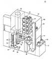
- FIG. 1is a schematic perspective view showing a substrate processing apparatus according to a first embodiment.
- FIG. 2is a plan view of major parts of the substrate processing apparatus of the first embodiment.
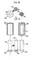
- FIG. 3is a schematic perspective view showing a SCARA arm used in the first embodiment.
- FIGS. 4A and 4Bare top views of the SCARA arm used in the first embodiment.
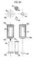
- FIGS. 5A through 5Iare views for explaining how to transfer boats used in the first embodiment.
- FIG. 6is a view showing the configuration of a controller used in the first embodiment.
- FIG. 7is a flowchart showing the actions of the controller used in the first embodiment.
- FIG. 8is a schematic perspective view showing a substrate processing apparatus according to a second embodiment.
- FIGS. 9A through 9Dillustrate a boat transfer flow in the substrate processing apparatus of the second embodiment, the lower part in each view being a side elevation of reactors, SCARA arms and their vicinities, and the upper part in each view being a cross section taken along line D-D.
- FIGS. 9E through 9Hare a continuation of the boat transfer flow in the substrate processing apparatus of the second embodiment illustrated in FIGS. 9A to 9D , the lower part in each view being a side elevation of reactors, SCARA arms and their vicinities, and the upper part in each view being a cross section taken along line D-D.
- FIGS. 9I through 9Lare a continuation of the boat transfer flow in the substrate processing apparatus of the second embodiment illustrated in FIGS. 9E to 9H , the lower part in each view being a side elevation of reactors, SCARA arms and their vicinities, and the upper part in each view being a cross section taken along line D-D.
- FIGS. 9M through 9Pare a continuation of the boat transfer flow in the substrate processing apparatus of the second embodiment illustrated in FIGS. 9I to 9L , the lower part in each view being a side elevation of reactors, SCARA arms and their vicinities, and the upper part in each view being a cross section taken along line D-D.
- FIG. 9Qis a continuation of the boat transfer flow in the substrate processing apparatus of the second embodiment illustrated in FIGS. 9M to 9P , the lower part in this view being a side elevation of reactors, SCARA arms and their vicinities, and the upper part in this view being a cross section taken along line D-D.
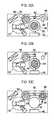
- FIG. 10is a schematic perspective view showing a substrate processing apparatus according to a comparative example.
- FIG. 11is a plan view of major parts of the substrate processing apparatus of the comparative example.
- FIGS. 12A through 12Gare views for explaining how to transfer boats used in the comparative example.
- FIG. 1is a perspective view of a two-boat-interchangeable substrate processing apparatus according to a first embodiment.
- FIG. 2is a plan view of the two-boat-interchangeable substrate processing apparatus.
- the substrate processing apparatus 10 of the first embodimentincludes a housing 12 having a gate 14 defined on the front surface thereof.
- a cassette delivery stage 16is provided outside and below the gate 14 .
- Two substrate storage cassettes 18may be placed on the cassette delivery stage 16 .
- the substrate storage cassettes 18may be plastic-made sealable containers. For example, twenty five substrates are loaded into the substrate storage cassettes 18 in multiple layers.
- a cassette loader 20is installed opposite to the gate 14 .
- the cassette loader 20is movable in any horizontal direction (e.g., back and forth or lateral directions) and vertical direction.
- the cassette loader 20is capable of conveying the substrate storage cassettes 18 to a cassette opener 22 or a cassette rack 24 , both of which will be described later.
- the cassette opener 22is provided at the opposite side of the cassette loader 20 from the gate 14 .
- the cassette opener 22is located off-center toward one lateral surface 26 of the housing 12 .
- the cassette opener 22includes a lifting table 28 on which the substrate storage cassettes 18 may be placed one above the other and a door opening/closing mechanism 30 configured to open a door (not shown) of the substrate storage cassettes 18 placed on the lifting table 28 .
- the cassette rack 24is of a rotary type and is provided above the cassette opener 22 .
- the substrate storage cassettes 18are conveyed to the cassette rack 24 by means of the cassette loader 20 .
- a substrate transfer machine 32is installed at the opposite side of the cassette opener 22 from the cassette loader 20 .
- the substrate transfer machine 32includes a pair of tweezers 34 configured to be movable backward/forward or rotatable.
- the substrate transfer machine 32may be moved upward and downward by a transfer machine elevator (not shown).
- a notch alignment device 36is provided between the cassette opener 22 and the substrate transfer machine 32 .
- the notch alignment device 36is used in aligning the substrates 38 held within the substrate storage cassettes 18 .
- a boat elevator 40is provided at the rear surface side of the substrate transfer machine 32 .
- the boat elevator 40includes a lifting arm 42 configured to be moved upward and downward by a lifting motor (not shown in the drawings).
- a reactor mouth cap 44is provided in the tip end portion of the lifting arm 42 .
- a boat table(not shown) of predetermined height may be placed on the upper surface of the reactor mouth cap 44 , thereby providing a boat transfer position.
- Substrate holders (boats) 48 and 49configured to horizontally hold processing-target substrates (e.g., wafers) 38 in multiple layers are placed on the boat table.
- the boats 48 and 49are made of, e.g., glass which is composed of quartz, silicon carbide, silicon and other substances.
- Each of the boats 48 and 49includes three columns 50 , e.g., made of quartz. 100 to 150 substrates 38 may be loaded to the slot defined by the columns 50 .
- a reactor 52 including a reaction chamber and a heateris provided above the reactor mouth cap 44 .
- the reactor 52has a reactor mouth (not shown) defined in the lower portion thereof. The position right below the reactor mouth becomes a boat loading/unloading position A and also a substrate loading/unloading position where the substrates 38 are loaded into or unloaded from the boats 48 and 49 . The first boat 48 and the second boat 49 are alternately loaded into and unloaded from the reactor mouth.
- the reactor mouth cap 44is fitted to the reactor mouth to seal the reactor 52 to be air-tight.
- the reactor 52includes a heater (not shown in the drawings). The substrates 38 are processed by the reactor 52 under the presence of a reaction gas.
- a first SCARA (Selective Compliant Assembly Robot Arm) arm 58 as a first boat conveying device and a second SCARA arm 60 as a second boat conveying deviceare provided in the inner rear area of the housing 12 in opposing relationship with the boat elevator 40 .
- the first SCARA arm 58 and the second SCARA arm 60will now be described with reference to FIGS. 3 , 4 A and 4 B.
- FIG. 3is a perspective view showing the first SCARA arm 58 or the second SCARA arm 60 used in the present embodiment.
- FIGS. 4A and 4Bare top views of the first SCARA arm 58 or the second SCARA arm 60 shown in FIG. 3 .
- FIG. 4Adepicts a standby state of the SCARA arms and
- FIG. 4Bdepicts a limited state of the SCARA arms.
- Each of the first SCARA arm 58 and the second SCARA arm 60includes a boat support portion 62 configured to support the boats 48 and 49 thereon, a first arm 64 configured to rotatably support the boat support portion 62 , a second arm 66 configured to rotatably support the first arm 64 and a base portion 68 configured to support the second arm 66 in a rotatable, vertically movable and back-and-forth movable manner.
- the boat support portion 62is shown to have a rectangular shape but may be formed to have, e.g., a U-shape. Also, in case of supporting the boats 48 and 49 , the surface of the boat support portion 62 facing the boats 48 and 49 may have a concave shape. At least three protrusions 70 are formed on the upper surface of the boat support portion 62 . The three protrusions 70 are inserted into the holes (not shown) formed on the lower surface of each of the boats 48 and 49 , whereby the boats 48 and 49 are reliably supported by the first SCARA arm 58 and the second SCARA arm 60 .
- each of the first SCARA arm 58 and the second SCARA arm 60waits in a folded state by the rotation of the respective components about their ends (i.e., in a standby state) and extends rectilinearly in a limited time (i.e., in a limited state).
- a boat support table 46configured to support the boats 48 and 49 is arranged in such a position that does not hinder the loading and unloading operation of the boat elevator 40 (a table retreat position D as shown in FIG. 2 ).
- the boat support table 46is movable from the table retreat position D to the boat loading/unloading position A right below the reactor 52 . While discharging a processed substrate or charging an unprocessed substrate, the boat support table 46 is moved to the boat loading/unloading position A.
- boat loading/unloading position AThe position right below the reactor 52 where the boats 48 and 49 are loaded into or unloaded from the reactor 52 is referred to as boat loading/unloading position A.
- boat standby position BThe position near the substrate transfer machine 32 facing the installation surface of the boat elevator 40 is referred to as boat standby position B.
- boat retreat position CThe position interposing the table retreat position D between itself and the boat standby position B is referred to as boat retreat position C.
- the first SCARA arm 58is arranged in the boat standby position B with the second SCARA arm 60 arranged in the boat retreat position C (see FIG. 2 ).
- the substrate storage cassette 18is brought onto the cassette delivery stage 16 by an external conveying device not shown in the drawings. Twenty five substrates 38 are charged into the substrate storage cassette 18 at a predetermined vertical pitch.
- the substrate storage cassette 18is an air-tight sealed container which can prevent infiltration of particles. Thus, even when the substrate storage cassette 18 is positioned outside the housing 12 , it can prevent contamination of particles.
- the substrate storage cassette 18is placed on the cassette opener 22 or conveyed to the cassette rack 24 by means of the cassette loader 20 .
- the door of the substrate storage cassette 18 placed on the lifting table 28is opened by the door opening/closing mechanism 30 .
- the substrate transfer machine 32is movable up and down, movable back and forth and rotatable.
- the substrate transfer machine 32is moved to a predetermined height by a transfer machine elevator.
- the tweezers 34are moved forward to grip one of the substrates 38 existing within the substrate storage cassette 18 . Then, the tweezers 34 are moved backwards to unload the substrate 38 .
- the tweezers 34are rotated and height-adjusted. Thereafter, the tweezers 34 enter the boat 48 or 49 to load the substrate 38 into the boat 48 or 49 in a horizontal posture.
- the first SCARA arm 58 and the second SCARA arm 60are individually movable in transverse, vertical and back-and-forth directions.
- the boat support table 46is independently movable from the table retreat position D to the boat loading/unloading position A in transverse and back-and-forth directions.
- FIGS. 5A through 5Iare top plan views of a conveying chamber of the substrate processing apparatus 10 .
- FIG. 6shows the configuration of a controller 84 as a control unit of the substrate processing apparatus 10 .
- the controller 84controls the first SCARA arm 58 , the second SCARA arm 60 , the boat support table 46 , the substrate transfer machine 32 and the boat elevator 40 through an input/output device 85 .
- FIG. 7shows a control flow performed by the controller 84 . In the following description, the operations of the respective parts in the substrate processing apparatus 10 of the present embodiment are controlled by the controller 84 .
- the first boat 48 holding a processed substrate 38is unloaded from the reactor 52 using the boat elevator 40 (step S 14 ).
- the second boat 49 holding an unprocessed substrate 38is supported by the first SCARA arm 58 and waits in the boat standby position B (step S 12 ).
- the unloaded first boat 48is supported by the action of the second SCARA arm 60 in the boat loading/unloading position A and is moved back to the boat retreat position C.
- the processed substrate 38 held in the first boat 48is cooled to a specified temperature (step S 15 ).
- the second boat 49is loaded into the reactor 52 by the boat elevator 40 (step S 13 ).
- the boat support table 46 arranged in the table retreat position Dis moved to the boat loading/unloading position A (step S 16 ).
- the first boat 48is supported by the action of the second SCARA arm 60 and conveyed onto the boat support table 46 arranged in the boat loading/unloading position A.
- the processed substrate 38 held in the first boat 48 by the action of the substrate transfer machine 32is discharged from the substrate storage cassette 18 placed on the cassette opener 22 (step S 17 ). If the processed substrate 38 is charged into the substrate storage cassette 18 , the cassette 18 is conveyed to the cassette delivery stage 16 by the cassette loader 20 and then taken out by an external conveying device. The substrate storage cassette 18 charged with unprocessed substrates 38 is transferred to the cassette opener 22 by the cassette loader 20 . The substrate transfer machine 32 transfers one of the unprocessed substrates 38 from the substrate storage cassette 18 to the empty first boat 48 arranged in the boat loading/unloading position A (step S).
- the first boat 48 holding the unprocessed substrate 38is supported by the action of the first SCARA arm 58 and waits in the boat standby position B (step S 12 ).
- the batch processing of the substratesis performed by repeating the steps illustrated in FIGS. 5A through 5I .
- FIG. 8is a schematic perspective view showing the substrate processing apparatus 100 of the second embodiment. Descriptions of the same elements or functions as the first embodiment will be omitted, and only different elements or functions of the substrate processing apparatus 100 of the second embodiment from the substrate processing apparatus 10 of the first embodiment will be described.
- each of the boat elevators 40includes a lifting arm 42 (not shown in FIG. 8 ).
- the lifting arms 42 of the boat elevators 40may be moved up and down by lifting motors (not shown in the drawings).
- Reactor mouth caps 44 a and 44 bare provided in the tip end portions of the lifting arms 42 .
- Substrate holders (boats) 48 , 49 and 51configured to horizontally hold processing-target substrates (e.g., wafers) 38 in multiple layers are placed on the upper surfaces of the reactor mouth caps 44 a and 44 b.
- first and second reactors 52 a and 52 beach including a reaction chamber and a heater are provided above the reactor mouth caps 44 a and 44 b , respectively.
- Each of the first and second reactors 52 a and 52 bhas a reactor mouth (not shown) defined in the lower portion thereof.
- the position right below the reactor mouth of the first reactor 52 abecomes a boat loading/unloading position A and also a substrate loading/unloading position where the substrates 38 are loaded into or unloaded from the boats 48 , 49 and 51 .
- the first boat 48 , the second boat 49 and the third boat 51are alternately loaded into and unloaded from the reactor mouths of the first and second reactors 52 a and 52 b .
- the reactor mouth caps 44 a and 44 bare fitted to the reactor mouths of the first and second reactors 52 a and 52 b to seal the first and second reactors 52 a and 52 b to be air-tight.
- the substrates 38are processed by the first and second reactors 52 a and 52 b under the presence of a reaction gas.
- a first SCARA arm 58 as a first boat conveying device and a second SCARA arm 60 as a second boat conveying deviceare provided below the first and second reactors 52 a and 52 b to face each other.
- a boat support table 46configured to support the boats 48 , 49 and 50 is provided below the first and second reactors 52 a and 52 b .
- the boat support table 46is movable from the position right below the first reactor 52 a to the position right below the second reactor 52 b.
- the boat support table 46is moved from a first boat loading/unloading position A right below the first reactor 52 a to a second boat loading/unloading position B right below the second reactor 52 b either when discharging a processed substrate or charging an unprocessed substrate (e.g., to the substrate storage cassette 18 ), when unloading the boat carrying a processed substrate from one of the first and second reactors 52 a and 52 b , or when loading the boat carrying an unprocessed substrate into one of the first and second reactors 52 a and 52 b.
- FIGS. 9A through 9Qare diagrams for explaining the operation of the substrate processing apparatus 100 of the second embodiment.
- the lower part in each diagramis a side elevational view of the reactors 52 a and 52 b and the SCARA arms 58 and 60
- the upper part in each diagramis a cross sectional view taken along line D-D in the lower part.
- the substrate processing apparatus 100is controlled by a controller 84 .
- the controller 84controls the first SCARA arm 58 , the second SCARA arm 60 , the boat support table 46 , the substrate transfer machine 32 and the heaters (not shown) of the reactors 52 a and 52 b through an input/output device 85 .
- the operations of the respective parts of the substrate processing apparatus 100 of the second embodimentare controlled by the controller 84 .
- first boat loading/unloading position AThe position right below the first reactor 52 a where the boats 48 , 49 and 51 are loaded into or unloaded from the first reactor 52 a is referred to as first boat loading/unloading position A.
- second boat loading/unloading position B(or boat standby position B).
- boat retreat position CThe retreat position of the second SCARA arm 60 provided opposite the first SCARA arm 58 located near the substrate transfer machine 32 is referred to as boat retreat position C.
- an unprocessed substrate 38is transferred (charged) to the empty first boat 48 arranged in the first boat loading/unloading position A (the first boat, step S 11 ).
- the empty first boat 48is placed on the boat support table 46 located in the first boat loading/unloading position A.
- the unprocessed substrate 38 held in the second boat 49is thermally treated within the first reactor 52 a
- the unprocessed substrate 38 held in the third boat 51is thermally treated within the second reactor 52 b.
- the first boat 48 holding the unprocessed substrate 38is moved to the second boat loading/unloading position B, i.e., the boat standby position B (the first boat, step S 12 ).
- the second boat 49 holding the processed substrate 38is unloaded from within the first reactor 52 a to the first boat loading/unloading position A by the boat elevator 40 (the second boat, step S 14 ).
- the first boat 48 holding the unprocessed substrate 38waits in the second boat loading/unloading position B, i.e., the boat standby position B.
- the second boat 49 holding the processed substrate 38is supported by the action of the second SCARA arm 60 and moved back to the boat retreat position C.
- the processed substrate 38 held in the second boat 49is cooled to a specified temperature (the second boat, step S 15 ).
- the first boat 48 holding the unprocessed substrate 38 and waiting in the second boat loading/unloading position B(the boat standby position B) is supported by the action of the first SCARA arm 58 and conveyed to the first boat loading/unloading position A.
- the first boat 48 holding the unprocessed substrate 38is loaded from the first boat loading/unloading position A into the first reactor 52 a by the boat elevator 40 (the first boat, step S 13 ).
- the boat support table 46is moved from the second boat loading/unloading position B (the boat standby position B) to the first boat loading/unloading position A.
- the unprocessed substrate 38 held in the first boat 48is thermally treated within the first reactor 52 a .
- the second boat 49 moved back to the boat retreat position Cis supported by the action of the second SCARA arm 60 and conveyed onto the boat support table 46 located in the first boat loading/unloading position A (the second boat, step S 16 ).
- the third boat 51 holding the processed substrate 38is unloaded from within the second reactor 52 b to the second boat loading/unloading position B by the boat elevator 40 (the third boat, step S 14 ).
- the third boat 51 holding the processed substrate 38is supported by the action of the second SCARA arm 60 , moved back to the boat retreat position C and cooled (the third boat, step S 15 ).
- the second boat 49 holding the processed substrate 38is supported by the action of the first SCARA arm 58 and conveyed from the first boat loading/unloading position A to the second boat loading/unloading position B, i.e., the boat standby position B (the second boat, step S 12 ).
- FIG. 9Oillustrates that the second boat 49 holding the processed substrate 38 is conveyed from the second boat loading/unloading position B into the second reactor 52 b by the boat elevator 40 and then thermally treated (the second boat, step S 13 ).
- the third boat 51which has been moved back to the boat retreat position C, is supported by the action of the second SCARA arm 60 and conveyed onto the boat support table 46 arranged in the first boat loading/unloading position A.
- the processed substrate 38 held in the third boat 51is returned (discharged) to the substrate storage cassette 18 (not shown in FIG. 8 ) placed on the cassette opener 22 (not shown in FIG. 8 ) (the third boat, step S 17 ).
- the batch processing of the substratesis performed by repeating the steps illustrated in FIGS. 9A through 9Q .
- FIG. 10is a schematic perspective view of a substrate processing apparatus 80 according to a comparative example.
- FIG. 11is a top plan view of the substrate processing apparatus 80 shown in FIG. 10 .
- same elements or functions as the above embodimentswill be omitted, and only elements or functions differing from the substrate processing apparatus 10 of the first embodiment will be described.
- the substrate processing apparatus 80 of the comparative exampleincludes one boat conveying device 82 for conveying wafers and two first and second boat support tables 84 and 86 for supporting boats.
- the boat conveying device 82includes two arms 88 and 90 semicircular in shape.
- the first boat support table 84is provided in the boat standby position B described earlier, and the second boat support table 86 is provided in the boat retreat position C.
- the two arms 88 and 90 of the boat conveying device 82are rotated and vertically moved to convey two boats 48 and 49 between the boat loading/unloading position A, the boat standby position B and the boat retreat position C.
- FIGS. 12A through 12Gare top plan views of a conveying chamber of the substrate processing apparatus 80 of the comparative example.
- the operations of the respective parts of the substrate processing apparatus 80 of the comparative exampleare controlled by a controller 84 .
- the first boat 48 holding a processed substrateis unloaded from the reactor 52 by the boat elevator 40 .
- the second boat 49 holding an unprocessed substrate 38is placed on the first boat support table 84 .
- the unloaded first boat 48is conveyed onto the second boat support table 86 by the second arm 90 of the boat conveying device 82 and is cooled.
- the second boat 49 waiting above the first boat support table 84is conveyed to the boat loading/unloading position A by the first arm 88 of the boat conveying device 82 and loaded into the reactor 52 by the boat elevator 40 .
- the processed substrate 38is subjected to cooling, and the first boat 48 placed on the second boat support table 86 is conveyed onto the first boat support table 84 by the second arm 90 of the boat conveying device 82 .
- the processed substrateis discharged from the first boat 48 placed on the first boat support table 84 (e.g., to the substrate storage cassette 18 ) by means of the substrate transfer machine 32 , and the unprocessed substrate is charged to the first boat 48 (e.g., from the substrate storage cassette 18 ).
- the substrate 38when operating two boats, the substrate 38 is charged and discharged in the position of the boat support table 84 , which is located apart from the position right below the reactor 52 . Further, when operating one boat, the substrate 38 is charged and discharged in the boat positioned right below the reactor 52 . This makes it necessary to coordinate the operations of charging and discharging the substrates at two different locations (e.g., the position of the boat support table 84 and the position right below the reactor 52 ).
- the charging and discharging operations of the substratescan be coordinated only in the position of the boat support table 86 right below the reactor 52 either when operating two boats or when operating one boat. This facilitates coordinating the charging and discharging operations of the substrates.
- the charging and discharging operations of the substratescan be coordinated only in the position of the boat support table 86 right below the reactor 52 a . This also facilitates coordinating the charging and discharging operations of the substrates.
- the substrate processing apparatus 10 or 100 of the first and second embodimentscan be arranged in a footprint-reducing manner.
- a two-boat-type or three-boat-type substrate processing apparatuscapable of reducing the space while increasing the throughput even when applied to a vertical substrate processing apparatus for processing wafers of large diameter, e.g., 450 mm. While the use of 450 mm-diameter wafers has been described above by way of example, the diameter of the substrate is not limited thereto but may be further increased.
- the two boat conveying devicescan simultaneously perform their respective operations within the conveying chamber, which is effective in increasing the throughput.
- the number of boat conveying devicesis not limited thereto but may be three or more.
- the boat support table 46has been described to move (e.g., at a predetermined speed) to the position right below the reactor 52 by way of example, the above embodiments are not limited thereto but may be applied to a case where the boat support table 46 is ejected to quickly reach the position right below the reactor 52 . Since the substrate processing apparatus of the above embodiments may make use of the configuration of the existing substrate processing apparatus, the above embodiments may be implemented without significant modifications in configuration.
- the above embodimentsmake it possible to increase the throughput while keeping the footprint layout reduced.
- the above embodimentsmay be employed in semiconductor manufacturing technology and, more particularly, heat treatment technology with which processing-target substrates are put into a processing chamber and processed in a heated state.
- the above embodimentsmay be effectively applied to a substrate processing apparatus in which semiconductor wafers for production of semiconductor integrated circuit devices (semiconductor devices) are subjected to oxidation, diffusion or ion implantation and then subjected to reflow, annealing and thermal-CVD film formation for carrier activation and planarization.
Landscapes
- Engineering & Computer Science (AREA)
- Physics & Mathematics (AREA)
- Condensed Matter Physics & Semiconductors (AREA)
- General Physics & Mathematics (AREA)
- Manufacturing & Machinery (AREA)
- Computer Hardware Design (AREA)
- Microelectronics & Electronic Packaging (AREA)
- Power Engineering (AREA)
- Robotics (AREA)
- Container, Conveyance, Adherence, Positioning, Of Wafer (AREA)
- Chemical Vapour Deposition (AREA)
Abstract
Description
- This application is based upon and claims the benefit of priority from Japanese Patent Application No. 2011-047473, filed on Mar. 4, 2011, and Japanese Patent Application No. 2010-116103, filed on May 20, 2010, the entire contents of which are incorporated herein by reference.
- Embodiments described herein relate to a substrate processing apparatus and method for processing substrates such as semiconductor substrates or glass substrates.
- In a substrate processing apparatus, e.g., a vertical CVD diffusion apparatus, for processing substrates with a vertical reactor, a boat holding a plurality of substrates is loaded into the reactor through the use of a boat elevator, so that the substrates are processed in the reactor.
- When using a substrate processing apparatus for processing substrates held by a boat, a two-boat type substrate processing apparatus can be used to improve throughput. This substrate processing apparatus is provided with two boats and is capable of efficiently processing substrates. In this apparatus, while one set of substrates held by one of the boats are being processed, the other set of substrates stored in a substrate storage cassette are transferred to the other boat. Also, when the one set of substrates are completely processed, the two boats are interchanged with each other to process the other set of substrates (see JP2003-31643A).
- In a one type of substrate processing apparatus, wafers of 300 mm in diameter are processed. In order to further improve throughput, it is required to use large-diameter wafers, e.g., 450 mm-diameter wafers. However, this results in an increase in the relative size of a carrier device of the substrate processing apparatus, an enlarged footprint and an increase in the substitution time and use amount of N2within a transfer chamber, thereby affecting productivity.
- The present disclosure provides some embodiments of a substrate processing apparatus and method that may satisfy two conflicting requirements, i.e., a throughput increase and a footprint reduction.
- According to one embodiment, there is provided a substrate processing apparatus, including a reactor; at least two boat conveying devices configured to convey at least two boats; at least one boat support table configured to support the at least two boats, the boat support table being movable to a position below the reactor; and a control unit configured to control the boat conveying devices such that when a first boat of the at least two boats supported by a first boat conveying device of the plurality of boat conveying devices holds a processed substrate processed by the reactor and is moved back to a position spaced apart from the reactor, a second boat of the at least two boats holding an unprocessed substrate is loaded into the reactor using a second boat conveying device of the at least two boat conveying devices.
- The control unit may control the movement of the boat support table to the position below the reactor, and control the boat conveying devices to convey the first boat to the boat support table using the first boat conveying device, to discharge the processed substrate held in the first boat, to charge the unprocessed substrate to be subsequently processed into the first boat and to cause the first boat to wait in the position spaced apart from the reactor using the second boat conveying device.
- According to another embodiment, there is provided a substrate processing method, including: holding a processed substrate processed by a reactor in a first boat; supporting the first boat with a first boat conveying device; moving the first boat conveying device to a position spaced apart from the reactor; moving a second boat into the reactor using a second boat conveying device, the second boat holding an unprocessed substrate.
- The method may further include moving at least one boat support table to a position below the reactor, conveying the first boat to the boat support table using the first boat conveying device, discharging the processed substrate held in the first boat, charging the unprocessed substrate to be subsequently processed into the first boat and causing the first boat to wait in the position spaced apart from the reactor using the second boat conveying device. According to still another embodiment, there is provided a substrate processing apparatus, including: at least two reactors; at least two boat conveying devices configured to convey at least two boats; at least one boat support table configured to support the at least two boats, the at least one boat support table being movable from a position below a first reactor of the at least two reactors to a position below a second reactor of the at least two reactors; and a control unit configured to control the boat conveying devices such that, when a first boat of the at least two boats supported by a first boat conveying device of the at least two boat conveying devices holds a processed substrate processed by the first reactor and the first boat conveying device is moved back to a position spaced apart from the reactors, a second boat of the at least two boats holding an unprocessed substrate is moved into the first reactor using a second boat conveying device of the at least two boat conveying devices, the at least one boat support table is moved from the position below the first reactor to the position below the second reactor, the first boat is conveyed to the at least one boat support table using the first boat conveying device, the processed substrate held in the first boat is discharged, the unprocessed substrate to be subsequently processed is charged and moved to the first boat, and the first boat is caused to wait in the position spaced apart from the reactors.
- With the above embodiments, it is possible to meet two conflicting requirements, i.e., a throughput increase and a footprint reduction.
FIG. 1 is a schematic perspective view showing a substrate processing apparatus according to a first embodiment.FIG. 2 is a plan view of major parts of the substrate processing apparatus of the first embodiment.FIG. 3 is a schematic perspective view showing a SCARA arm used in the first embodiment.FIGS. 4A and 4B are top views of the SCARA arm used in the first embodiment.FIGS. 5A through 5I are views for explaining how to transfer boats used in the first embodiment.FIG. 6 is a view showing the configuration of a controller used in the first embodiment.FIG. 7 is a flowchart showing the actions of the controller used in the first embodiment.FIG. 8 is a schematic perspective view showing a substrate processing apparatus according to a second embodiment.FIGS. 9A through 9D illustrate a boat transfer flow in the substrate processing apparatus of the second embodiment, the lower part in each view being a side elevation of reactors, SCARA arms and their vicinities, and the upper part in each view being a cross section taken along line D-D.FIGS. 9E through 9H are a continuation of the boat transfer flow in the substrate processing apparatus of the second embodiment illustrated inFIGS. 9A to 9D , the lower part in each view being a side elevation of reactors, SCARA arms and their vicinities, and the upper part in each view being a cross section taken along line D-D.FIGS. 9I through 9L are a continuation of the boat transfer flow in the substrate processing apparatus of the second embodiment illustrated inFIGS. 9E to 9H , the lower part in each view being a side elevation of reactors, SCARA arms and their vicinities, and the upper part in each view being a cross section taken along line D-D.FIGS. 9M through 9P are a continuation of the boat transfer flow in the substrate processing apparatus of the second embodiment illustrated inFIGS. 9I to 9L , the lower part in each view being a side elevation of reactors, SCARA arms and their vicinities, and the upper part in each view being a cross section taken along line D-D.FIG. 9Q is a continuation of the boat transfer flow in the substrate processing apparatus of the second embodiment illustrated inFIGS. 9M to 9P , the lower part in this view being a side elevation of reactors, SCARA arms and their vicinities, and the upper part in this view being a cross section taken along line D-D.FIG. 10 is a schematic perspective view showing a substrate processing apparatus according to a comparative example.FIG. 11 is a plan view of major parts of the substrate processing apparatus of the comparative example.FIGS. 12A through 12G are views for explaining how to transfer boats used in the comparative example.- Certain embodiments will now be described in detail with reference to the accompanying drawings.
FIG. 1 is a perspective view of a two-boat-interchangeable substrate processing apparatus according to a first embodiment.FIG. 2 is a plan view of the two-boat-interchangeable substrate processing apparatus. - The
substrate processing apparatus 10 of the first embodiment includes ahousing 12 having agate 14 defined on the front surface thereof. Acassette delivery stage 16 is provided outside and below thegate 14. Twosubstrate storage cassettes 18 may be placed on thecassette delivery stage 16. Thesubstrate storage cassettes 18 may be plastic-made sealable containers. For example, twenty five substrates are loaded into thesubstrate storage cassettes 18 in multiple layers. - A
cassette loader 20 is installed opposite to thegate 14. Thecassette loader 20 is movable in any horizontal direction (e.g., back and forth or lateral directions) and vertical direction. Thecassette loader 20 is capable of conveying thesubstrate storage cassettes 18 to acassette opener 22 or acassette rack 24, both of which will be described later. - The
cassette opener 22 is provided at the opposite side of thecassette loader 20 from thegate 14. Thecassette opener 22 is located off-center toward onelateral surface 26 of thehousing 12. - The
cassette opener 22 includes a lifting table28 on which thesubstrate storage cassettes 18 may be placed one above the other and a door opening/closing mechanism 30 configured to open a door (not shown) of thesubstrate storage cassettes 18 placed on the lifting table28. - The
cassette rack 24 is of a rotary type and is provided above thecassette opener 22. Thesubstrate storage cassettes 18 are conveyed to thecassette rack 24 by means of thecassette loader 20. - A
substrate transfer machine 32 is installed at the opposite side of thecassette opener 22 from thecassette loader 20. Thesubstrate transfer machine 32 includes a pair oftweezers 34 configured to be movable backward/forward or rotatable. Thesubstrate transfer machine 32 may be moved upward and downward by a transfer machine elevator (not shown). - A
notch alignment device 36 is provided between thecassette opener 22 and thesubstrate transfer machine 32. Thenotch alignment device 36 is used in aligning thesubstrates 38 held within thesubstrate storage cassettes 18. - A
boat elevator 40 is provided at the rear surface side of thesubstrate transfer machine 32. Theboat elevator 40 includes a liftingarm 42 configured to be moved upward and downward by a lifting motor (not shown in the drawings). - A
reactor mouth cap 44 is provided in the tip end portion of the liftingarm 42. A boat table (not shown) of predetermined height may be placed on the upper surface of thereactor mouth cap 44, thereby providing a boat transfer position. Substrate holders (boats)48 and49 configured to horizontally hold processing-target substrates (e.g., wafers)38 in multiple layers are placed on the boat table. Theboats boats columns 50, e.g., made of quartz.100 to150substrates 38 may be loaded to the slot defined by thecolumns 50. - A
reactor 52 including a reaction chamber and a heater is provided above thereactor mouth cap 44. Thereactor 52 has a reactor mouth (not shown) defined in the lower portion thereof. The position right below the reactor mouth becomes a boat loading/unloading position A and also a substrate loading/unloading position where thesubstrates 38 are loaded into or unloaded from theboats first boat 48 and thesecond boat 49 are alternately loaded into and unloaded from the reactor mouth. Thereactor mouth cap 44 is fitted to the reactor mouth to seal thereactor 52 to be air-tight. Thereactor 52 includes a heater (not shown in the drawings). Thesubstrates 38 are processed by thereactor 52 under the presence of a reaction gas. - A first SCARA (Selective Compliant Assembly Robot Arm)
arm 58 as a first boat conveying device and asecond SCARA arm 60 as a second boat conveying device are provided in the inner rear area of thehousing 12 in opposing relationship with theboat elevator 40. Thefirst SCARA arm 58 and thesecond SCARA arm 60 will now be described with reference toFIGS. 3 ,4A and4B. FIG. 3 is a perspective view showing thefirst SCARA arm 58 or thesecond SCARA arm 60 used in the present embodiment.FIGS. 4A and 4B are top views of thefirst SCARA arm 58 or thesecond SCARA arm 60 shown inFIG. 3 .FIG. 4A depicts a standby state of the SCARA arms andFIG. 4B depicts a limited state of the SCARA arms.- Each of the
first SCARA arm 58 and thesecond SCARA arm 60 includes aboat support portion 62 configured to support theboats first arm 64 configured to rotatably support theboat support portion 62, asecond arm 66 configured to rotatably support thefirst arm 64 and abase portion 68 configured to support thesecond arm 66 in a rotatable, vertically movable and back-and-forth movable manner. - The
boat support portion 62 is shown to have a rectangular shape but may be formed to have, e.g., a U-shape. Also, in case of supporting theboats boat support portion 62 facing theboats protrusions 70 are formed on the upper surface of theboat support portion 62. The threeprotrusions 70 are inserted into the holes (not shown) formed on the lower surface of each of theboats boats first SCARA arm 58 and thesecond SCARA arm 60. - In other words, the
boat support portion 62 is rotatably supported at its end by thefirst arm 64 which in turn is rotatably supported at its end by thesecond arm 66 which in turn is rotatably supported at its end by thebase portion 68. Thus, each of thefirst SCARA arm 58 and thesecond SCARA arm 60 waits in a folded state by the rotation of the respective components about their ends (i.e., in a standby state) and extends rectilinearly in a limited time (i.e., in a limited state). - A boat support table46 configured to support the
boats FIG. 2 ). The boat support table46 is movable from the table retreat position D to the boat loading/unloading position A right below thereactor 52. While discharging a processed substrate or charging an unprocessed substrate, the boat support table46 is moved to the boat loading/unloading position A. - Next, description will be made on the operations of the
substrate processing apparatus 10 of the first embodiment. - The position right below the
reactor 52 where theboats reactor 52 is referred to as boat loading/unloading position A. The position near thesubstrate transfer machine 32 facing the installation surface of theboat elevator 40 is referred to as boat standby position B. The position interposing the table retreat position D between itself and the boat standby position B is referred to as boat retreat position C. Thefirst SCARA arm 58 is arranged in the boat standby position B with thesecond SCARA arm 60 arranged in the boat retreat position C (seeFIG. 2 ). - The
substrate storage cassette 18 is brought onto thecassette delivery stage 16 by an external conveying device not shown in the drawings. Twenty fivesubstrates 38 are charged into thesubstrate storage cassette 18 at a predetermined vertical pitch. Thesubstrate storage cassette 18 is an air-tight sealed container which can prevent infiltration of particles. Thus, even when thesubstrate storage cassette 18 is positioned outside thehousing 12, it can prevent contamination of particles. - The
substrate storage cassette 18 is placed on thecassette opener 22 or conveyed to thecassette rack 24 by means of thecassette loader 20. The door of thesubstrate storage cassette 18 placed on the lifting table28 is opened by the door opening/closing mechanism 30. - The
substrate transfer machine 32 is movable up and down, movable back and forth and rotatable. Thesubstrate transfer machine 32 is moved to a predetermined height by a transfer machine elevator. Thetweezers 34 are moved forward to grip one of thesubstrates 38 existing within thesubstrate storage cassette 18. Then, thetweezers 34 are moved backwards to unload thesubstrate 38. - The
tweezers 34 are rotated and height-adjusted. Thereafter, thetweezers 34 enter theboat substrate 38 into theboat - The
first SCARA arm 58 and thesecond SCARA arm 60 are individually movable in transverse, vertical and back-and-forth directions. The boat support table46 is independently movable from the table retreat position D to the boat loading/unloading position A in transverse and back-and-forth directions. - Next, description will be made on the operations of the
first SCARA arm 58 and thesecond SCARA arm 60. FIGS. 5A through 5I are top plan views of a conveying chamber of thesubstrate processing apparatus 10.FIG. 6 shows the configuration of acontroller 84 as a control unit of thesubstrate processing apparatus 10. Thecontroller 84 controls thefirst SCARA arm 58, thesecond SCARA arm 60, the boat support table46, thesubstrate transfer machine 32 and theboat elevator 40 through an input/output device 85.FIG. 7 shows a control flow performed by thecontroller 84. In the following description, the operations of the respective parts in thesubstrate processing apparatus 10 of the present embodiment are controlled by thecontroller 84.- As shown in
FIG. 5A , thefirst boat 48 holding a processedsubstrate 38 is unloaded from thereactor 52 using the boat elevator40 (step S14). At this time, thesecond boat 49 holding anunprocessed substrate 38 is supported by thefirst SCARA arm 58 and waits in the boat standby position B (step S12). - As shown in
FIGS. 5B and 5C , the unloadedfirst boat 48 is supported by the action of thesecond SCARA arm 60 in the boat loading/unloading position A and is moved back to the boat retreat position C. The processedsubstrate 38 held in thefirst boat 48 is cooled to a specified temperature (step S15). - Then, as shown in
FIGS. 5D and 5E , while the processedsubstrate 38 held in thefirst boat 48 is being cooled in the boat retreat position C, thesecond boat 49 holding theunprocessed substrate 38 and waiting in the boat standby position B is supported by the action of thefirst SCARA arm 58 and conveyed to the boat loading/unloading position A. - As shown in
FIG. 5F , thesecond boat 49 is loaded into thereactor 52 by the boat elevator40 (step S13). The boat support table46 arranged in the table retreat position D is moved to the boat loading/unloading position A (step S16). - As shown in
FIG. 5G , if the processedsubstrate 38 held in the first boat48 (which has been moved back to the boat retreat position C) is cooled to the specified temperature, thefirst boat 48 is supported by the action of thesecond SCARA arm 60 and conveyed onto the boat support table46 arranged in the boat loading/unloading position A. - Thereafter, as shown in
FIG. 5H , the processedsubstrate 38 held in thefirst boat 48 by the action of thesubstrate transfer machine 32 is discharged from thesubstrate storage cassette 18 placed on the cassette opener22 (step S17). If the processedsubstrate 38 is charged into thesubstrate storage cassette 18, thecassette 18 is conveyed to thecassette delivery stage 16 by thecassette loader 20 and then taken out by an external conveying device. Thesubstrate storage cassette 18 charged withunprocessed substrates 38 is transferred to thecassette opener 22 by thecassette loader 20. Thesubstrate transfer machine 32 transfers one of theunprocessed substrates 38 from thesubstrate storage cassette 18 to the emptyfirst boat 48 arranged in the boat loading/unloading position A (step S). - As shown in
FIG. 5I , thefirst boat 48 holding theunprocessed substrate 38 is supported by the action of thefirst SCARA arm 58 and waits in the boat standby position B (step S12). - The batch processing of the substrates is performed by repeating the steps illustrated in
FIGS. 5A through 5I . - Next, description will be made on a two-reactor three-boat-interchangeable substrate processing apparatus according to a second embodiment.
FIG. 8 is a schematic perspective view showing thesubstrate processing apparatus 100 of the second embodiment. Descriptions of the same elements or functions as the first embodiment will be omitted, and only different elements or functions of thesubstrate processing apparatus 100 of the second embodiment from thesubstrate processing apparatus 10 of the first embodiment will be described. - In the
substrate processing apparatus 100 of the second embodiment, two boat elevators40 (not shown inFIG. 8 ) are provided at the rear surface side of thesubstrate transfer machine 32. Each of theboat elevators 40 includes a lifting arm42 (not shown inFIG. 8 ). The liftingarms 42 of theboat elevators 40 may be moved up and down by lifting motors (not shown in the drawings). - Reactor mouth caps44aand44b(not shown in
FIG. 8 ) are provided in the tip end portions of the liftingarms 42. Substrate holders (boats)48,49 and51 configured to horizontally hold processing-target substrates (e.g., wafers)38 in multiple layers are placed on the upper surfaces of the reactor mouth caps44aand44b. - In the
substrate processing apparatus 100 of the second embodiment, two reactors, i.e., first andsecond reactors - Each of the first and
second reactors first reactor 52abecomes a boat loading/unloading position A and also a substrate loading/unloading position where thesubstrates 38 are loaded into or unloaded from theboats first boat 48, thesecond boat 49 and thethird boat 51 are alternately loaded into and unloaded from the reactor mouths of the first andsecond reactors second reactors second reactors substrates 38 are processed by the first andsecond reactors - A
first SCARA arm 58 as a first boat conveying device and asecond SCARA arm 60 as a second boat conveying device are provided below the first andsecond reactors - A boat support table46 configured to support the
boats second reactors first reactor 52ato the position right below thesecond reactor 52b. - The boat support table46 is moved from a first boat loading/unloading position A right below the
first reactor 52ato a second boat loading/unloading position B right below thesecond reactor 52beither when discharging a processed substrate or charging an unprocessed substrate (e.g., to the substrate storage cassette18), when unloading the boat carrying a processed substrate from one of the first andsecond reactors second reactors - Description will now be made on the operations of the
first SCARA arm 58 and thesecond SCARA arm 60 in thesubstrate processing apparatus 100 of the second embodiment. FIGS. 9A through 9Q are diagrams for explaining the operation of thesubstrate processing apparatus 100 of the second embodiment. The lower part in each diagram is a side elevational view of thereactors SCARA arms substrate processing apparatus 100 is controlled by acontroller 84. Thecontroller 84 controls thefirst SCARA arm 58, thesecond SCARA arm 60, the boat support table46, thesubstrate transfer machine 32 and the heaters (not shown) of thereactors output device 85. In the following description, the operations of the respective parts of thesubstrate processing apparatus 100 of the second embodiment are controlled by thecontroller 84.- The position right below the
first reactor 52awhere theboats first reactor 52ais referred to as first boat loading/unloading position A. The position right below thesecond reactor 52bis referred to as a second boat loading/unloading position B (or boat standby position B). The retreat position of thesecond SCARA arm 60 provided opposite thefirst SCARA arm 58 located near thesubstrate transfer machine 32 is referred to as boat retreat position C. - A shown in
FIGS. 9A and 9B , by the action of thesubstrate transfer machine 32, anunprocessed substrate 38 is transferred (charged) to the emptyfirst boat 48 arranged in the first boat loading/unloading position A (the first boat, step S11). At this time, the emptyfirst boat 48 is placed on the boat support table46 located in the first boat loading/unloading position A. Theunprocessed substrate 38 held in thesecond boat 49 is thermally treated within thefirst reactor 52a, and theunprocessed substrate 38 held in thethird boat 51 is thermally treated within thesecond reactor 52b. - Then, as shown in
FIG. 9C , by the action of the boat support table46, thefirst boat 48 holding theunprocessed substrate 38 is moved to the second boat loading/unloading position B, i.e., the boat standby position B (the first boat, step S12). - As shown in
FIG. 9D , thesecond boat 49 holding the processedsubstrate 38 is unloaded from within thefirst reactor 52ato the first boat loading/unloading position A by the boat elevator40 (the second boat, step S14). At this time, thefirst boat 48 holding theunprocessed substrate 38 waits in the second boat loading/unloading position B, i.e., the boat standby position B. - Thereafter, as shown in
FIGS. 9E and 9F , thesecond boat 49 holding the processedsubstrate 38 is supported by the action of thesecond SCARA arm 60 and moved back to the boat retreat position C. The processedsubstrate 38 held in thesecond boat 49 is cooled to a specified temperature (the second boat, step S15). - Referring to
FIG. 9G , while the processedsubstrate 38 held in thesecond boat 49 is being cooled in the boat retreat position C, thefirst boat 48 holding theunprocessed substrate 38 and waiting in the second boat loading/unloading position B (the boat standby position B) is supported by the action of thefirst SCARA arm 58 and conveyed to the first boat loading/unloading position A. - As illustrated in
FIG. 9H , thefirst boat 48 holding theunprocessed substrate 38 is loaded from the first boat loading/unloading position A into thefirst reactor 52aby the boat elevator40 (the first boat, step S13). - As shown in
FIGS. 9I and 9J , the boat support table46 is moved from the second boat loading/unloading position B (the boat standby position B) to the first boat loading/unloading position A. At this time, theunprocessed substrate 38 held in thefirst boat 48 is thermally treated within thefirst reactor 52a. Thesecond boat 49 moved back to the boat retreat position C is supported by the action of thesecond SCARA arm 60 and conveyed onto the boat support table46 located in the first boat loading/unloading position A (the second boat, step S16). - As shown in
FIG. 9K , thethird boat 51 holding the processedsubstrate 38 is unloaded from within thesecond reactor 52bto the second boat loading/unloading position B by the boat elevator40 (the third boat, step S14). - As shown in
FIGS. 9L and 9M , thethird boat 51 holding the processedsubstrate 38 is supported by the action of thesecond SCARA arm 60, moved back to the boat retreat position C and cooled (the third boat, step S15). - Then, as shown in
FIG. 9N , thesecond boat 49 holding the processedsubstrate 38 is supported by the action of thefirst SCARA arm 58 and conveyed from the first boat loading/unloading position A to the second boat loading/unloading position B, i.e., the boat standby position B (the second boat, step S12). FIG. 9O illustrates that thesecond boat 49 holding the processedsubstrate 38 is conveyed from the second boat loading/unloading position B into thesecond reactor 52bby theboat elevator 40 and then thermally treated (the second boat, step S13).- As shown in
FIG. 9P , thethird boat 51, which has been moved back to the boat retreat position C, is supported by the action of thesecond SCARA arm 60 and conveyed onto the boat support table46 arranged in the first boat loading/unloading position A. - As shown in
FIG. 9Q , by the action of thesubstrate transfer machine 32, the processedsubstrate 38 held in thethird boat 51 is returned (discharged) to the substrate storage cassette18 (not shown inFIG. 8 ) placed on the cassette opener22 (not shown inFIG. 8 ) (the third boat, step S17). - The batch processing of the substrates is performed by repeating the steps illustrated in
FIGS. 9A through 9Q . - Next, description will be made on a
substrate processing apparatus 80 according to a comparative example of thesubstrate processing apparatus 10 of the present embodiment.FIG. 10 is a schematic perspective view of asubstrate processing apparatus 80 according to a comparative example.FIG. 11 is a top plan view of thesubstrate processing apparatus 80 shown inFIG. 10 . In the following description, same elements or functions as the above embodiments will be omitted, and only elements or functions differing from thesubstrate processing apparatus 10 of the first embodiment will be described. - The
substrate processing apparatus 80 of the comparative example includes oneboat conveying device 82 for conveying wafers and two first and second boat support tables84 and86 for supporting boats. Theboat conveying device 82 includes twoarms arms boat conveying device 82 are rotated and vertically moved to convey twoboats FIGS. 12A through 12G are top plan views of a conveying chamber of thesubstrate processing apparatus 80 of the comparative example. In the following description, the operations of the respective parts of thesubstrate processing apparatus 80 of the comparative example are controlled by acontroller 84.- As shown in
FIG. 12A , thefirst boat 48 holding a processed substrate is unloaded from thereactor 52 by theboat elevator 40. At this time, thesecond boat 49 holding anunprocessed substrate 38 is placed on the first boat support table84. - Then, as shown in
FIGS. 12B and 12C , the unloadedfirst boat 48 is conveyed onto the second boat support table86 by thesecond arm 90 of theboat conveying device 82 and is cooled. - Referring to
FIGS. 12D and 12E , while the processedsubstrate 38 is cooled, thesecond boat 49 waiting above the first boat support table84 is conveyed to the boat loading/unloading position A by thefirst arm 88 of theboat conveying device 82 and loaded into thereactor 52 by theboat elevator 40. - As shown in
FIG. 12F , the processedsubstrate 38 is subjected to cooling, and thefirst boat 48 placed on the second boat support table86 is conveyed onto the first boat support table84 by thesecond arm 90 of theboat conveying device 82. - Then, as shown in
FIG. 12G , the processed substrate is discharged from thefirst boat 48 placed on the first boat support table84 (e.g., to the substrate storage cassette18) by means of thesubstrate transfer machine 32, and the unprocessed substrate is charged to the first boat48 (e.g., from the substrate storage cassette18). - In the two-boat-type
substrate processing apparatus 80 of the comparative example described above with reference toFIGS. 10 through 12G , when operating two boats, thesubstrate 38 is charged and discharged in the position of the boat support table84, which is located apart from the position right below thereactor 52. Further, when operating one boat, thesubstrate 38 is charged and discharged in the boat positioned right below thereactor 52. This makes it necessary to coordinate the operations of charging and discharging the substrates at two different locations (e.g., the position of the boat support table84 and the position right below the reactor52). With the two-boat-typesubstrate processing apparatus 10 of the first embodiment, however, the charging and discharging operations of the substrates can be coordinated only in the position of the boat support table86 right below thereactor 52 either when operating two boats or when operating one boat. This facilitates coordinating the charging and discharging operations of the substrates. Similarly, with the three-boat-typesubstrate processing apparatus 100 of the second embodiment, the charging and discharging operations of the substrates can be coordinated only in the position of the boat support table86 right below thereactor 52a. This also facilitates coordinating the charging and discharging operations of the substrates. - As compared with the
substrate processing apparatus 80 of the comparative example, thesubstrate processing apparatus reactor 52 by way of example, the above embodiments are not limited thereto but may be applied to a case where the boat support table46 is ejected to quickly reach the position right below thereactor 52. Since the substrate processing apparatus of the above embodiments may make use of the configuration of the existing substrate processing apparatus, the above embodiments may be implemented without significant modifications in configuration. - Accordingly, the above embodiments make it possible to increase the throughput while keeping the footprint layout reduced.
- The above embodiments may be employed in semiconductor manufacturing technology and, more particularly, heat treatment technology with which processing-target substrates are put into a processing chamber and processed in a heated state. For example, the above embodiments may be effectively applied to a substrate processing apparatus in which semiconductor wafers for production of semiconductor integrated circuit devices (semiconductor devices) are subjected to oxidation, diffusion or ion implantation and then subjected to reflow, annealing and thermal-CVD film formation for carrier activation and planarization.
- While certain embodiments have been described above, these embodiments have been presented by way of example only, and are not intended to limit the scope of the inventions. Indeed, the novel substrate processing apparatus and method described herein may be embodied in a variety of other forms; furthermore, various omissions, substitutions and changes in the form of the substrate processing apparatus and method described herein may be made without departing from the sprit of the inventions. The accompanying claims and their equivalents are intended to cover such forms or modifications as would fall within the scope and sprit of the inventions.
Claims (6)
1. A substrate processing apparatus, comprising:
a reactor;
at least two boat conveying devices configured to convey at least two boats;
at least one boat support table configured to support the at least two boats, the boat support table being movable to a position below the reactor; and
a control unit configured to control the boat conveying devices such that when a first boat of the at least two boats supported by a first boat conveying device of the plurality of boat conveying devices holds a processed substrate processed by the reactor and is moved back to a position spaced apart from the reactor, a second boat of the at least two boats holding an unprocessed substrate is loaded into the reactor using a second boat conveying device of the at least two boat conveying devices.
2. The apparatus ofclaim 1 , wherein the control unit controls the movement of the boat support table to the position below the reactor, and controls the boat conveying devices to convey the first boat to the boat support table using the first boat conveying device, to discharge the processed substrate held in the first boat, to charge the unprocessed substrate to be subsequently processed into the first boat and to cause the first boat to wait in the position spaced apart from the reactor using the second boat conveying device.
3. A substrate processing apparatus, comprising:
at least two reactors;
at least two boat conveying devices configured to convey at least two boats;
at least one boat support table configured to support the at least two boats, the at least one boat support table being movable from a position below a first reactor of the at least two reactors to a position below a second reactor of the at least two reactors; and
a control unit configured to control the boat conveying devices such that, when a first boat of the at least two boats supported by a first boat conveying device of the at least two boat conveying devices holds a processed substrate processed by the first reactor and the first boat conveying device is moved back to a position spaced apart from the reactors, a second boat of the at least two boats holding an unprocessed substrate is moved into the first reactor using a second boat conveying device of the at least two boat conveying devices, the at least one boat support table is moved from the position below the first reactor to the position below the second reactor, the first boat is conveyed to the at least one boat support table using the first boat conveying device, the processed substrate held in the first boat is discharged, the unprocessed substrate to be subsequently processed is charged and moved to the first boat, and the first boat is caused to wait in the position spaced apart from the reactors.
4. A substrate processing method in a substrate processing apparatus comprising a first reactor and a second reactor, the method comprising:
holding a processed substrate processed by a first reactor in a first boat;
supporting the first boat with a first boat conveying device;
moving the first boat conveying device to a position spaced apart from the first and second reactors;
moving a second boat into the first reactor using a second boat conveying device, the second boat holding an unprocessed substrate.
5. The method ofclaim 4 , further comprising:
moving a boat support table from the position below the first reactor to the position below the second reactor; and
conveying the first boat to the boat support table using the first boat conveying device.
6. The method ofclaim 5 , further comprising:
discharging the processed substrate held in the first boat;
charging a unprocessed substrate to be subsequently processed into the first boat;
moving the first boat to the position spaced apart from the first and second reactors using the second boat conveying device.
Applications Claiming Priority (4)
| Application Number | Priority Date | Filing Date | Title |
|---|---|---|---|
| JP2010-116103 | 2010-05-20 | ||
| JP2010116103 | 2010-05-20 | ||
| JP2011047473AJP2012004536A (en) | 2010-05-20 | 2011-03-04 | Substrate treatment apparatus and substrate treatment method |
| JP2011-047473 | 2011-03-04 |
Publications (1)
| Publication Number | Publication Date |
|---|---|
| US20110286819A1true US20110286819A1 (en) | 2011-11-24 |
Family
ID=44972609
Family Applications (1)
| Application Number | Title | Priority Date | Filing Date |
|---|---|---|---|
| US13/109,566AbandonedUS20110286819A1 (en) | 2010-05-20 | 2011-05-17 | Substrate processing apparatus and substrate processing method |
Country Status (4)
| Country | Link |
|---|---|
| US (1) | US20110286819A1 (en) |
| JP (1) | JP2012004536A (en) |
| KR (1) | KR20110128149A (en) |
| CN (1) | CN102254848A (en) |
Cited By (253)
| Publication number | Priority date | Publication date | Assignee | Title |
|---|---|---|---|---|
| US20130175908A1 (en)* | 2012-01-10 | 2013-07-11 | Sheng-Jung Chang | Wafer Stocker |
| US20160035607A1 (en)* | 2014-07-30 | 2016-02-04 | Samsung Electronics Co., Ltd. | Semiconductor wafer stocker apparatus and wafer transferring methods using the same |
| US11164955B2 (en) | 2017-07-18 | 2021-11-02 | Asm Ip Holding B.V. | Methods for forming a semiconductor device structure and related semiconductor device structures |
| US11171025B2 (en) | 2019-01-22 | 2021-11-09 | Asm Ip Holding B.V. | Substrate processing device |
| US11168395B2 (en) | 2018-06-29 | 2021-11-09 | Asm Ip Holding B.V. | Temperature-controlled flange and reactor system including same |
| US11217444B2 (en) | 2018-11-30 | 2022-01-04 | Asm Ip Holding B.V. | Method for forming an ultraviolet radiation responsive metal oxide-containing film |
| US11222772B2 (en) | 2016-12-14 | 2022-01-11 | Asm Ip Holding B.V. | Substrate processing apparatus |
| USD940837S1 (en) | 2019-08-22 | 2022-01-11 | Asm Ip Holding B.V. | Electrode |
| US11227782B2 (en)* | 2019-07-31 | 2022-01-18 | Asm Ip Holding B.V. | Vertical batch furnace assembly |
| US11227789B2 (en) | 2019-02-20 | 2022-01-18 | Asm Ip Holding B.V. | Method and apparatus for filling a recess formed within a substrate surface |
| US11233133B2 (en) | 2015-10-21 | 2022-01-25 | Asm Ip Holding B.V. | NbMC layers |
| US11230766B2 (en) | 2018-03-29 | 2022-01-25 | Asm Ip Holding B.V. | Substrate processing apparatus and method |
| US11232963B2 (en) | 2018-10-03 | 2022-01-25 | Asm Ip Holding B.V. | Substrate processing apparatus and method |
| US11242598B2 (en) | 2015-06-26 | 2022-02-08 | Asm Ip Holding B.V. | Structures including metal carbide material, devices including the structures, and methods of forming same |
| US11251040B2 (en) | 2019-02-20 | 2022-02-15 | Asm Ip Holding B.V. | Cyclical deposition method including treatment step and apparatus for same |
| US11251035B2 (en) | 2016-12-22 | 2022-02-15 | Asm Ip Holding B.V. | Method of forming a structure on a substrate |
| US11251068B2 (en) | 2018-10-19 | 2022-02-15 | Asm Ip Holding B.V. | Substrate processing apparatus and substrate processing method |
| USD944946S1 (en) | 2019-06-14 | 2022-03-01 | Asm Ip Holding B.V. | Shower plate |
| US11270899B2 (en) | 2018-06-04 | 2022-03-08 | Asm Ip Holding B.V. | Wafer handling chamber with moisture reduction |
| US11274369B2 (en) | 2018-09-11 | 2022-03-15 | Asm Ip Holding B.V. | Thin film deposition method |
| US11282698B2 (en) | 2019-07-19 | 2022-03-22 | Asm Ip Holding B.V. | Method of forming topology-controlled amorphous carbon polymer film |
| US11286562B2 (en) | 2018-06-08 | 2022-03-29 | Asm Ip Holding B.V. | Gas-phase chemical reactor and method of using same |
| US11286558B2 (en) | 2019-08-23 | 2022-03-29 | Asm Ip Holding B.V. | Methods for depositing a molybdenum nitride film on a surface of a substrate by a cyclical deposition process and related semiconductor device structures including a molybdenum nitride film |
| US11289326B2 (en) | 2019-05-07 | 2022-03-29 | Asm Ip Holding B.V. | Method for reforming amorphous carbon polymer film |
| US11295980B2 (en) | 2017-08-30 | 2022-04-05 | Asm Ip Holding B.V. | Methods for depositing a molybdenum metal film over a dielectric surface of a substrate by a cyclical deposition process and related semiconductor device structures |
| USD947913S1 (en) | 2019-05-17 | 2022-04-05 | Asm Ip Holding B.V. | Susceptor shaft |
| US11296189B2 (en) | 2018-06-21 | 2022-04-05 | Asm Ip Holding B.V. | Method for depositing a phosphorus doped silicon arsenide film and related semiconductor device structures |
| US11306395B2 (en) | 2017-06-28 | 2022-04-19 | Asm Ip Holding B.V. | Methods for depositing a transition metal nitride film on a substrate by atomic layer deposition and related deposition apparatus |
| USD949319S1 (en) | 2019-08-22 | 2022-04-19 | Asm Ip Holding B.V. | Exhaust duct |
| US11315794B2 (en) | 2019-10-21 | 2022-04-26 | Asm Ip Holding B.V. | Apparatus and methods for selectively etching films |
| US11342216B2 (en) | 2019-02-20 | 2022-05-24 | Asm Ip Holding B.V. | Cyclical deposition method and apparatus for filling a recess formed within a substrate surface |
| US11339476B2 (en) | 2019-10-08 | 2022-05-24 | Asm Ip Holding B.V. | Substrate processing device having connection plates, substrate processing method |
| US11345999B2 (en) | 2019-06-06 | 2022-05-31 | Asm Ip Holding B.V. | Method of using a gas-phase reactor system including analyzing exhausted gas |
| US11355338B2 (en) | 2019-05-10 | 2022-06-07 | Asm Ip Holding B.V. | Method of depositing material onto a surface and structure formed according to the method |
| US11361990B2 (en) | 2018-05-28 | 2022-06-14 | Asm Ip Holding B.V. | Substrate processing method and device manufactured by using the same |
| US11374112B2 (en) | 2017-07-19 | 2022-06-28 | Asm Ip Holding B.V. | Method for depositing a group IV semiconductor and related semiconductor device structures |
| US11378337B2 (en) | 2019-03-28 | 2022-07-05 | Asm Ip Holding B.V. | Door opener and substrate processing apparatus provided therewith |
| US11387120B2 (en) | 2017-09-28 | 2022-07-12 | Asm Ip Holding B.V. | Chemical dispensing apparatus and methods for dispensing a chemical to a reaction chamber |
| US11387106B2 (en) | 2018-02-14 | 2022-07-12 | Asm Ip Holding B.V. | Method for depositing a ruthenium-containing film on a substrate by a cyclical deposition process |
| US11390950B2 (en) | 2017-01-10 | 2022-07-19 | Asm Ip Holding B.V. | Reactor system and method to reduce residue buildup during a film deposition process |
| US11390946B2 (en) | 2019-01-17 | 2022-07-19 | Asm Ip Holding B.V. | Methods of forming a transition metal containing film on a substrate by a cyclical deposition process |
| US11390945B2 (en) | 2019-07-03 | 2022-07-19 | Asm Ip Holding B.V. | Temperature control assembly for substrate processing apparatus and method of using same |
| US11393690B2 (en) | 2018-01-19 | 2022-07-19 | Asm Ip Holding B.V. | Deposition method |
| US11398382B2 (en) | 2018-03-27 | 2022-07-26 | Asm Ip Holding B.V. | Method of forming an electrode on a substrate and a semiconductor device structure including an electrode |
| US11396702B2 (en) | 2016-11-15 | 2022-07-26 | Asm Ip Holding B.V. | Gas supply unit and substrate processing apparatus including the gas supply unit |
| US11401605B2 (en) | 2019-11-26 | 2022-08-02 | Asm Ip Holding B.V. | Substrate processing apparatus |
| US11410851B2 (en) | 2017-02-15 | 2022-08-09 | Asm Ip Holding B.V. | Methods for forming a metallic film on a substrate by cyclical deposition and related semiconductor device structures |
| US11411088B2 (en) | 2018-11-16 | 2022-08-09 | Asm Ip Holding B.V. | Methods for forming a metal silicate film on a substrate in a reaction chamber and related semiconductor device structures |
| US11417545B2 (en) | 2017-08-08 | 2022-08-16 | Asm Ip Holding B.V. | Radiation shield |
| US11414760B2 (en) | 2018-10-08 | 2022-08-16 | Asm Ip Holding B.V. | Substrate support unit, thin film deposition apparatus including the same, and substrate processing apparatus including the same |
| US11424119B2 (en) | 2019-03-08 | 2022-08-23 | Asm Ip Holding B.V. | Method for selective deposition of silicon nitride layer and structure including selectively-deposited silicon nitride layer |
| US11430640B2 (en) | 2019-07-30 | 2022-08-30 | Asm Ip Holding B.V. | Substrate processing apparatus |
| US11430674B2 (en) | 2018-08-22 | 2022-08-30 | Asm Ip Holding B.V. | Sensor array, apparatus for dispensing a vapor phase reactant to a reaction chamber and related methods |
| US11437241B2 (en) | 2020-04-08 | 2022-09-06 | Asm Ip Holding B.V. | Apparatus and methods for selectively etching silicon oxide films |
| US11443926B2 (en) | 2019-07-30 | 2022-09-13 | Asm Ip Holding B.V. | Substrate processing apparatus |
| US11447861B2 (en) | 2016-12-15 | 2022-09-20 | Asm Ip Holding B.V. | Sequential infiltration synthesis apparatus and a method of forming a patterned structure |
| US11447864B2 (en) | 2019-04-19 | 2022-09-20 | Asm Ip Holding B.V. | Layer forming method and apparatus |
| US11450529B2 (en) | 2019-11-26 | 2022-09-20 | Asm Ip Holding B.V. | Methods for selectively forming a target film on a substrate comprising a first dielectric surface and a second metallic surface |
| USD965044S1 (en) | 2019-08-19 | 2022-09-27 | Asm Ip Holding B.V. | Susceptor shaft |
| US11453943B2 (en) | 2016-05-25 | 2022-09-27 | Asm Ip Holding B.V. | Method for forming carbon-containing silicon/metal oxide or nitride film by ALD using silicon precursor and hydrocarbon precursor |
| USD965524S1 (en) | 2019-08-19 | 2022-10-04 | Asm Ip Holding B.V. | Susceptor support |
| US11469098B2 (en) | 2018-05-08 | 2022-10-11 | Asm Ip Holding B.V. | Methods for depositing an oxide film on a substrate by a cyclical deposition process and related device structures |
| US11476109B2 (en) | 2019-06-11 | 2022-10-18 | Asm Ip Holding B.V. | Method of forming an electronic structure using reforming gas, system for performing the method, and structure formed using the method |
| US11473195B2 (en) | 2018-03-01 | 2022-10-18 | Asm Ip Holding B.V. | Semiconductor processing apparatus and a method for processing a substrate |
| US11482412B2 (en) | 2018-01-19 | 2022-10-25 | Asm Ip Holding B.V. | Method for depositing a gap-fill layer by plasma-assisted deposition |
| US11482418B2 (en) | 2018-02-20 | 2022-10-25 | Asm Ip Holding B.V. | Substrate processing method and apparatus |
| US11482533B2 (en) | 2019-02-20 | 2022-10-25 | Asm Ip Holding B.V. | Apparatus and methods for plug fill deposition in 3-D NAND applications |
| US11488854B2 (en) | 2020-03-11 | 2022-11-01 | Asm Ip Holding B.V. | Substrate handling device with adjustable joints |
| US11488819B2 (en) | 2018-12-04 | 2022-11-01 | Asm Ip Holding B.V. | Method of cleaning substrate processing apparatus |
| US11495459B2 (en) | 2019-09-04 | 2022-11-08 | Asm Ip Holding B.V. | Methods for selective deposition using a sacrificial capping layer |
| US11492703B2 (en) | 2018-06-27 | 2022-11-08 | Asm Ip Holding B.V. | Cyclic deposition methods for forming metal-containing material and films and structures including the metal-containing material |
| US11501956B2 (en) | 2012-10-12 | 2022-11-15 | Asm Ip Holding B.V. | Semiconductor reaction chamber showerhead |
| US11499226B2 (en) | 2018-11-02 | 2022-11-15 | Asm Ip Holding B.V. | Substrate supporting unit and a substrate processing device including the same |
| US11501973B2 (en) | 2018-01-16 | 2022-11-15 | Asm Ip Holding B.V. | Method for depositing a material film on a substrate within a reaction chamber by a cyclical deposition process and related device structures |
| US11499222B2 (en) | 2018-06-27 | 2022-11-15 | Asm Ip Holding B.V. | Cyclic deposition methods for forming metal-containing material and films and structures including the metal-containing material |
| US11501968B2 (en) | 2019-11-15 | 2022-11-15 | Asm Ip Holding B.V. | Method for providing a semiconductor device with silicon filled gaps |
| US11515187B2 (en) | 2020-05-01 | 2022-11-29 | Asm Ip Holding B.V. | Fast FOUP swapping with a FOUP handler |
| US11515188B2 (en)* | 2019-05-16 | 2022-11-29 | Asm Ip Holding B.V. | Wafer boat handling device, vertical batch furnace and method |
| US11521851B2 (en) | 2020-02-03 | 2022-12-06 | Asm Ip Holding B.V. | Method of forming structures including a vanadium or indium layer |
| US11527403B2 (en) | 2019-12-19 | 2022-12-13 | Asm Ip Holding B.V. | Methods for filling a gap feature on a substrate surface and related semiconductor structures |
| US11527400B2 (en) | 2019-08-23 | 2022-12-13 | Asm Ip Holding B.V. | Method for depositing silicon oxide film having improved quality by peald using bis(diethylamino)silane |
| US11532757B2 (en) | 2016-10-27 | 2022-12-20 | Asm Ip Holding B.V. | Deposition of charge trapping layers |
| US11530483B2 (en) | 2018-06-21 | 2022-12-20 | Asm Ip Holding B.V. | Substrate processing system |
| US11530876B2 (en) | 2020-04-24 | 2022-12-20 | Asm Ip Holding B.V. | Vertical batch furnace assembly comprising a cooling gas supply |
| US11551912B2 (en) | 2020-01-20 | 2023-01-10 | Asm Ip Holding B.V. | Method of forming thin film and method of modifying surface of thin film |
| US11551925B2 (en) | 2019-04-01 | 2023-01-10 | Asm Ip Holding B.V. | Method for manufacturing a semiconductor device |
| US11557474B2 (en) | 2019-07-29 | 2023-01-17 | Asm Ip Holding B.V. | Methods for selective deposition utilizing n-type dopants and/or alternative dopants to achieve high dopant incorporation |
| USD975665S1 (en) | 2019-05-17 | 2023-01-17 | Asm Ip Holding B.V. | Susceptor shaft |
| US11562901B2 (en) | 2019-09-25 | 2023-01-24 | Asm Ip Holding B.V. | Substrate processing method |
| US11572620B2 (en) | 2018-11-06 | 2023-02-07 | Asm Ip Holding B.V. | Methods for selectively depositing an amorphous silicon film on a substrate |
| US11581186B2 (en) | 2016-12-15 | 2023-02-14 | Asm Ip Holding B.V. | Sequential infiltration synthesis apparatus |
| US11587814B2 (en) | 2019-07-31 | 2023-02-21 | Asm Ip Holding B.V. | Vertical batch furnace assembly |
| US11587821B2 (en) | 2017-08-08 | 2023-02-21 | Asm Ip Holding B.V. | Substrate lift mechanism and reactor including same |
| US11587815B2 (en) | 2019-07-31 | 2023-02-21 | Asm Ip Holding B.V. | Vertical batch furnace assembly |
| USD979506S1 (en) | 2019-08-22 | 2023-02-28 | Asm Ip Holding B.V. | Insulator |
| US11594600B2 (en) | 2019-11-05 | 2023-02-28 | Asm Ip Holding B.V. | Structures with doped semiconductor layers and methods and systems for forming same |
| US11594450B2 (en) | 2019-08-22 | 2023-02-28 | Asm Ip Holding B.V. | Method for forming a structure with a hole |
| USD980813S1 (en) | 2021-05-11 | 2023-03-14 | Asm Ip Holding B.V. | Gas flow control plate for substrate processing apparatus |
| US11605528B2 (en) | 2019-07-09 | 2023-03-14 | Asm Ip Holding B.V. | Plasma device using coaxial waveguide, and substrate treatment method |
| USD980814S1 (en) | 2021-05-11 | 2023-03-14 | Asm Ip Holding B.V. | Gas distributor for substrate processing apparatus |
| US11610775B2 (en) | 2016-07-28 | 2023-03-21 | Asm Ip Holding B.V. | Method and apparatus for filling a gap |
| US11610774B2 (en) | 2019-10-02 | 2023-03-21 | Asm Ip Holding B.V. | Methods for forming a topographically selective silicon oxide film by a cyclical plasma-enhanced deposition process |
| US11615970B2 (en) | 2019-07-17 | 2023-03-28 | Asm Ip Holding B.V. | Radical assist ignition plasma system and method |
| USD981973S1 (en) | 2021-05-11 | 2023-03-28 | Asm Ip Holding B.V. | Reactor wall for substrate processing apparatus |
| US11626316B2 (en) | 2019-11-20 | 2023-04-11 | Asm Ip Holding B.V. | Method of depositing carbon-containing material on a surface of a substrate, structure formed using the method, and system for forming the structure |
| US11626308B2 (en) | 2020-05-13 | 2023-04-11 | Asm Ip Holding B.V. | Laser alignment fixture for a reactor system |
| US11629407B2 (en) | 2019-02-22 | 2023-04-18 | Asm Ip Holding B.V. | Substrate processing apparatus and method for processing substrates |
| US11629406B2 (en) | 2018-03-09 | 2023-04-18 | Asm Ip Holding B.V. | Semiconductor processing apparatus comprising one or more pyrometers for measuring a temperature of a substrate during transfer of the substrate |
| US11637011B2 (en) | 2019-10-16 | 2023-04-25 | Asm Ip Holding B.V. | Method of topology-selective film formation of silicon oxide |
| US11637014B2 (en) | 2019-10-17 | 2023-04-25 | Asm Ip Holding B.V. | Methods for selective deposition of doped semiconductor material |
| US11639811B2 (en) | 2017-11-27 | 2023-05-02 | Asm Ip Holding B.V. | Apparatus including a clean mini environment |
| US11639548B2 (en) | 2019-08-21 | 2023-05-02 | Asm Ip Holding B.V. | Film-forming material mixed-gas forming device and film forming device |
| US11646204B2 (en) | 2020-06-24 | 2023-05-09 | Asm Ip Holding B.V. | Method for forming a layer provided with silicon |
| US11646205B2 (en) | 2019-10-29 | 2023-05-09 | Asm Ip Holding B.V. | Methods of selectively forming n-type doped material on a surface, systems for selectively forming n-type doped material, and structures formed using same |
| US11646184B2 (en) | 2019-11-29 | 2023-05-09 | Asm Ip Holding B.V. | Substrate processing apparatus |
| US11646197B2 (en) | 2018-07-03 | 2023-05-09 | Asm Ip Holding B.V. | Method for depositing silicon-free carbon-containing film as gap-fill layer by pulse plasma-assisted deposition |
| US11644758B2 (en) | 2020-07-17 | 2023-05-09 | Asm Ip Holding B.V. | Structures and methods for use in photolithography |
| US11643724B2 (en) | 2019-07-18 | 2023-05-09 | Asm Ip Holding B.V. | Method of forming structures using a neutral beam |
| US11649546B2 (en) | 2016-07-08 | 2023-05-16 | Asm Ip Holding B.V. | Organic reactants for atomic layer deposition |
| US11658029B2 (en) | 2018-12-14 | 2023-05-23 | Asm Ip Holding B.V. | Method of forming a device structure using selective deposition of gallium nitride and system for same |
| US11658035B2 (en) | 2020-06-30 | 2023-05-23 | Asm Ip Holding B.V. | Substrate processing method |
| US11664267B2 (en) | 2019-07-10 | 2023-05-30 | Asm Ip Holding B.V. | Substrate support assembly and substrate processing device including the same |
| US11664245B2 (en) | 2019-07-16 | 2023-05-30 | Asm Ip Holding B.V. | Substrate processing device |
| US11664199B2 (en) | 2018-10-19 | 2023-05-30 | Asm Ip Holding B.V. | Substrate processing apparatus and substrate processing method |
| US11676812B2 (en) | 2016-02-19 | 2023-06-13 | Asm Ip Holding B.V. | Method for forming silicon nitride film selectively on top/bottom portions |
| US11674220B2 (en) | 2020-07-20 | 2023-06-13 | Asm Ip Holding B.V. | Method for depositing molybdenum layers using an underlayer |
| US11680839B2 (en) | 2019-08-05 | 2023-06-20 | Asm Ip Holding B.V. | Liquid level sensor for a chemical source vessel |
| US11682572B2 (en) | 2017-11-27 | 2023-06-20 | Asm Ip Holdings B.V. | Storage device for storing wafer cassettes for use with a batch furnace |
| US11688603B2 (en) | 2019-07-17 | 2023-06-27 | Asm Ip Holding B.V. | Methods of forming silicon germanium structures |
| US11685991B2 (en) | 2018-02-14 | 2023-06-27 | Asm Ip Holding B.V. | Method for depositing a ruthenium-containing film on a substrate by a cyclical deposition process |
| USD990534S1 (en) | 2020-09-11 | 2023-06-27 | Asm Ip Holding B.V. | Weighted lift pin |
| USD990441S1 (en) | 2021-09-07 | 2023-06-27 | Asm Ip Holding B.V. | Gas flow control plate |
| US11694892B2 (en) | 2016-07-28 | 2023-07-04 | Asm Ip Holding B.V. | Method and apparatus for filling a gap |
| US11705333B2 (en) | 2020-05-21 | 2023-07-18 | Asm Ip Holding B.V. | Structures including multiple carbon layers and methods of forming and using same |
| US11718913B2 (en) | 2018-06-04 | 2023-08-08 | Asm Ip Holding B.V. | Gas distribution system and reactor system including same |
| US11725277B2 (en) | 2011-07-20 | 2023-08-15 | Asm Ip Holding B.V. | Pressure transmitter for a semiconductor processing environment |
| US11725280B2 (en) | 2020-08-26 | 2023-08-15 | Asm Ip Holding B.V. | Method for forming metal silicon oxide and metal silicon oxynitride layers |
| US11735414B2 (en) | 2018-02-06 | 2023-08-22 | Asm Ip Holding B.V. | Method of post-deposition treatment for silicon oxide film |
| US11735445B2 (en) | 2018-10-31 | 2023-08-22 | Asm Ip Holding B.V. | Substrate processing apparatus for processing substrates |
| US11735422B2 (en) | 2019-10-10 | 2023-08-22 | Asm Ip Holding B.V. | Method of forming a photoresist underlayer and structure including same |
| US11742189B2 (en) | 2015-03-12 | 2023-08-29 | Asm Ip Holding B.V. | Multi-zone reactor, system including the reactor, and method of using the same |
| US11742198B2 (en) | 2019-03-08 | 2023-08-29 | Asm Ip Holding B.V. | Structure including SiOCN layer and method of forming same |
| US11749562B2 (en) | 2016-07-08 | 2023-09-05 | Asm Ip Holding B.V. | Selective deposition method to form air gaps |
| US11769670B2 (en) | 2018-12-13 | 2023-09-26 | Asm Ip Holding B.V. | Methods for forming a rhenium-containing film on a substrate by a cyclical deposition process and related semiconductor device structures |
| US11769682B2 (en) | 2017-08-09 | 2023-09-26 | Asm Ip Holding B.V. | Storage apparatus for storing cassettes for substrates and processing apparatus equipped therewith |
| US11767589B2 (en) | 2020-05-29 | 2023-09-26 | Asm Ip Holding B.V. | Substrate processing device |
| US11776846B2 (en) | 2020-02-07 | 2023-10-03 | Asm Ip Holding B.V. | Methods for depositing gap filling fluids and related systems and devices |
| US11781221B2 (en) | 2019-05-07 | 2023-10-10 | Asm Ip Holding B.V. | Chemical source vessel with dip tube |
| US11781243B2 (en) | 2020-02-17 | 2023-10-10 | Asm Ip Holding B.V. | Method for depositing low temperature phosphorous-doped silicon |
| US11795545B2 (en) | 2014-10-07 | 2023-10-24 | Asm Ip Holding B.V. | Multiple temperature range susceptor, assembly, reactor and system including the susceptor, and methods of using the same |
| US11802338B2 (en) | 2017-07-26 | 2023-10-31 | Asm Ip Holding B.V. | Chemical treatment, deposition and/or infiltration apparatus and method for using the same |
| US11804364B2 (en) | 2020-05-19 | 2023-10-31 | Asm Ip Holding B.V. | Substrate processing apparatus |
| US11804388B2 (en) | 2018-09-11 | 2023-10-31 | Asm Ip Holding B.V. | Substrate processing apparatus and method |
| US11810788B2 (en) | 2016-11-01 | 2023-11-07 | Asm Ip Holding B.V. | Methods for forming a transition metal niobium nitride film on a substrate by atomic layer deposition and related semiconductor device structures |
| US11814747B2 (en) | 2019-04-24 | 2023-11-14 | Asm Ip Holding B.V. | Gas-phase reactor system-with a reaction chamber, a solid precursor source vessel, a gas distribution system, and a flange assembly |
| US11823876B2 (en) | 2019-09-05 | 2023-11-21 | Asm Ip Holding B.V. | Substrate processing apparatus |
| US11823866B2 (en) | 2020-04-02 | 2023-11-21 | Asm Ip Holding B.V. | Thin film forming method |
| US11821078B2 (en) | 2020-04-15 | 2023-11-21 | Asm Ip Holding B.V. | Method for forming precoat film and method for forming silicon-containing film |
| US11830738B2 (en) | 2020-04-03 | 2023-11-28 | Asm Ip Holding B.V. | Method for forming barrier layer and method for manufacturing semiconductor device |
| US11828707B2 (en) | 2020-02-04 | 2023-11-28 | Asm Ip Holding B.V. | Method and apparatus for transmittance measurements of large articles |
| US11830730B2 (en) | 2017-08-29 | 2023-11-28 | Asm Ip Holding B.V. | Layer forming method and apparatus |
| US11827981B2 (en) | 2020-10-14 | 2023-11-28 | Asm Ip Holding B.V. | Method of depositing material on stepped structure |
| US11840761B2 (en) | 2019-12-04 | 2023-12-12 | Asm Ip Holding B.V. | Substrate processing apparatus |
| US11848200B2 (en) | 2017-05-08 | 2023-12-19 | Asm Ip Holding B.V. | Methods for selectively forming a silicon nitride film on a substrate and related semiconductor device structures |
| US11876356B2 (en) | 2020-03-11 | 2024-01-16 | Asm Ip Holding B.V. | Lockout tagout assembly and system and method of using same |
| US11873557B2 (en) | 2020-10-22 | 2024-01-16 | Asm Ip Holding B.V. | Method of depositing vanadium metal |
| US11885020B2 (en) | 2020-12-22 | 2024-01-30 | Asm Ip Holding B.V. | Transition metal deposition method |
| US11887857B2 (en) | 2020-04-24 | 2024-01-30 | Asm Ip Holding B.V. | Methods and systems for depositing a layer comprising vanadium, nitrogen, and a further element |
| US11885023B2 (en) | 2018-10-01 | 2024-01-30 | Asm Ip Holding B.V. | Substrate retaining apparatus, system including the apparatus, and method of using same |
| USD1012873S1 (en) | 2020-09-24 | 2024-01-30 | Asm Ip Holding B.V. | Electrode for semiconductor processing apparatus |
| US11885013B2 (en) | 2019-12-17 | 2024-01-30 | Asm Ip Holding B.V. | Method of forming vanadium nitride layer and structure including the vanadium nitride layer |
| US11891696B2 (en) | 2020-11-30 | 2024-02-06 | Asm Ip Holding B.V. | Injector configured for arrangement within a reaction chamber of a substrate processing apparatus |
| US11901179B2 (en) | 2020-10-28 | 2024-02-13 | Asm Ip Holding B.V. | Method and device for depositing silicon onto substrates |
| US11898243B2 (en) | 2020-04-24 | 2024-02-13 | Asm Ip Holding B.V. | Method of forming vanadium nitride-containing layer |
| US11923190B2 (en) | 2018-07-03 | 2024-03-05 | Asm Ip Holding B.V. | Method for depositing silicon-free carbon-containing film as gap-fill layer by pulse plasma-assisted deposition |
| US11923181B2 (en) | 2019-11-29 | 2024-03-05 | Asm Ip Holding B.V. | Substrate processing apparatus for minimizing the effect of a filling gas during substrate processing |
| US11929251B2 (en) | 2019-12-02 | 2024-03-12 | Asm Ip Holding B.V. | Substrate processing apparatus having electrostatic chuck and substrate processing method |
| US11939673B2 (en) | 2018-02-23 | 2024-03-26 | Asm Ip Holding B.V. | Apparatus for detecting or monitoring for a chemical precursor in a high temperature environment |
| US11946137B2 (en) | 2020-12-16 | 2024-04-02 | Asm Ip Holding B.V. | Runout and wobble measurement fixtures |
| US11956977B2 (en) | 2015-12-29 | 2024-04-09 | Asm Ip Holding B.V. | Atomic layer deposition of III-V compounds to form V-NAND devices |
| US11959168B2 (en) | 2020-04-29 | 2024-04-16 | Asm Ip Holding B.V. | Solid source precursor vessel |
| US11961741B2 (en) | 2020-03-12 | 2024-04-16 | Asm Ip Holding B.V. | Method for fabricating layer structure having target topological profile |
| US11967488B2 (en) | 2013-02-01 | 2024-04-23 | Asm Ip Holding B.V. | Method for treatment of deposition reactor |
| USD1023959S1 (en) | 2021-05-11 | 2024-04-23 | Asm Ip Holding B.V. | Electrode for substrate processing apparatus |
| US11976359B2 (en) | 2020-01-06 | 2024-05-07 | Asm Ip Holding B.V. | Gas supply assembly, components thereof, and reactor system including same |
| US11987881B2 (en) | 2020-05-22 | 2024-05-21 | Asm Ip Holding B.V. | Apparatus for depositing thin films using hydrogen peroxide |
| US11986868B2 (en) | 2020-02-28 | 2024-05-21 | Asm Ip Holding B.V. | System dedicated for parts cleaning |
| US11993847B2 (en) | 2020-01-08 | 2024-05-28 | Asm Ip Holding B.V. | Injector |
| US11996292B2 (en) | 2019-10-25 | 2024-05-28 | Asm Ip Holding B.V. | Methods for filling a gap feature on a substrate surface and related semiconductor structures |
| US11996309B2 (en) | 2019-05-16 | 2024-05-28 | Asm Ip Holding B.V. | Wafer boat handling device, vertical batch furnace and method |
| US11996289B2 (en) | 2020-04-16 | 2024-05-28 | Asm Ip Holding B.V. | Methods of forming structures including silicon germanium and silicon layers, devices formed using the methods, and systems for performing the methods |
| US12009224B2 (en) | 2020-09-29 | 2024-06-11 | Asm Ip Holding B.V. | Apparatus and method for etching metal nitrides |
| US12006572B2 (en) | 2019-10-08 | 2024-06-11 | Asm Ip Holding B.V. | Reactor system including a gas distribution assembly for use with activated species and method of using same |
| US12009241B2 (en) | 2019-10-14 | 2024-06-11 | Asm Ip Holding B.V. | Vertical batch furnace assembly with detector to detect cassette |
| US12020934B2 (en) | 2020-07-08 | 2024-06-25 | Asm Ip Holding B.V. | Substrate processing method |
| US12025484B2 (en) | 2018-05-08 | 2024-07-02 | Asm Ip Holding B.V. | Thin film forming method |
| US12027365B2 (en) | 2020-11-24 | 2024-07-02 | Asm Ip Holding B.V. | Methods for filling a gap and related systems and devices |
| US12033885B2 (en) | 2020-01-06 | 2024-07-09 | Asm Ip Holding B.V. | Channeled lift pin |
| US12033861B2 (en) | 2017-10-05 | 2024-07-09 | Asm Ip Holding B.V. | Method for selectively depositing a metallic film on a substrate |
| US12040177B2 (en) | 2020-08-18 | 2024-07-16 | Asm Ip Holding B.V. | Methods for forming a laminate film by cyclical plasma-enhanced deposition processes |
| US12040184B2 (en) | 2017-10-30 | 2024-07-16 | Asm Ip Holding B.V. | Methods for forming a semiconductor structure and related semiconductor structures |
| US12040199B2 (en) | 2018-11-28 | 2024-07-16 | Asm Ip Holding B.V. | Substrate processing apparatus for processing substrates |
| US12040200B2 (en) | 2017-06-20 | 2024-07-16 | Asm Ip Holding B.V. | Semiconductor processing apparatus and methods for calibrating a semiconductor processing apparatus |
| US12051567B2 (en) | 2020-10-07 | 2024-07-30 | Asm Ip Holding B.V. | Gas supply unit and substrate processing apparatus including gas supply unit |
| US12051602B2 (en) | 2020-05-04 | 2024-07-30 | Asm Ip Holding B.V. | Substrate processing system for processing substrates with an electronics module located behind a door in a front wall of the substrate processing system |
| US12057314B2 (en) | 2020-05-15 | 2024-08-06 | Asm Ip Holding B.V. | Methods for silicon germanium uniformity control using multiple precursors |
| US12068154B2 (en) | 2020-04-13 | 2024-08-20 | Asm Ip Holding B.V. | Method of forming a nitrogen-containing carbon film and system for performing the method |
| US12074022B2 (en) | 2020-08-27 | 2024-08-27 | Asm Ip Holding B.V. | Method and system for forming patterned structures using multiple patterning process |
| US12087586B2 (en) | 2020-04-15 | 2024-09-10 | Asm Ip Holding B.V. | Method of forming chromium nitride layer and structure including the chromium nitride layer |
| US12107005B2 (en) | 2020-10-06 | 2024-10-01 | Asm Ip Holding B.V. | Deposition method and an apparatus for depositing a silicon-containing material |
| US12106944B2 (en) | 2020-06-02 | 2024-10-01 | Asm Ip Holding B.V. | Rotating substrate support |
| US12112940B2 (en) | 2019-07-19 | 2024-10-08 | Asm Ip Holding B.V. | Method of forming topology-controlled amorphous carbon polymer film |
| US12125700B2 (en) | 2020-01-16 | 2024-10-22 | Asm Ip Holding B.V. | Method of forming high aspect ratio features |
| US12131885B2 (en) | 2020-12-22 | 2024-10-29 | Asm Ip Holding B.V. | Plasma treatment device having matching box |
| US12129545B2 (en) | 2020-12-22 | 2024-10-29 | Asm Ip Holding B.V. | Precursor capsule, a vessel and a method |
| US12148609B2 (en) | 2020-09-16 | 2024-11-19 | Asm Ip Holding B.V. | Silicon oxide deposition method |
| US12154824B2 (en) | 2020-08-14 | 2024-11-26 | Asm Ip Holding B.V. | Substrate processing method |
| US12159788B2 (en) | 2020-12-14 | 2024-12-03 | Asm Ip Holding B.V. | Method of forming structures for threshold voltage control |
| US12169361B2 (en) | 2019-07-30 | 2024-12-17 | Asm Ip Holding B.V. | Substrate processing apparatus and method |
| US12173404B2 (en) | 2020-03-17 | 2024-12-24 | Asm Ip Holding B.V. | Method of depositing epitaxial material, structure formed using the method, and system for performing the method |
| US12173402B2 (en) | 2018-02-15 | 2024-12-24 | Asm Ip Holding B.V. | Method of forming a transition metal containing film on a substrate by a cyclical deposition process, a method for supplying a transition metal halide compound to a reaction chamber, and related vapor deposition apparatus |
| US12195852B2 (en) | 2020-11-23 | 2025-01-14 | Asm Ip Holding B.V. | Substrate processing apparatus with an injector |
| US12203166B2 (en) | 2020-05-07 | 2025-01-21 | Asm Ip Holding B.V. | Apparatus and methods for performing an in-situ etch of reaction chambers with fluorine-based radicals |
| US12211742B2 (en) | 2020-09-10 | 2025-01-28 | Asm Ip Holding B.V. | Methods for depositing gap filling fluid |
| US12209308B2 (en) | 2020-11-12 | 2025-01-28 | Asm Ip Holding B.V. | Reactor and related methods |
| USD1060598S1 (en) | 2021-12-03 | 2025-02-04 | Asm Ip Holding B.V. | Split showerhead cover |
| US12218000B2 (en) | 2020-09-25 | 2025-02-04 | Asm Ip Holding B.V. | Semiconductor processing method |
| US12217946B2 (en) | 2020-10-15 | 2025-02-04 | Asm Ip Holding B.V. | Method of manufacturing semiconductor device, and substrate treatment apparatus using ether-CAT |
| US12218269B2 (en) | 2020-02-13 | 2025-02-04 | Asm Ip Holding B.V. | Substrate processing apparatus including light receiving device and calibration method of light receiving device |
| US12217954B2 (en) | 2020-08-25 | 2025-02-04 | Asm Ip Holding B.V. | Method of cleaning a surface |
| US12221357B2 (en) | 2020-04-24 | 2025-02-11 | Asm Ip Holding B.V. | Methods and apparatus for stabilizing vanadium compounds |
| US12230531B2 (en) | 2018-04-09 | 2025-02-18 | Asm Ip Holding B.V. | Substrate supporting apparatus, substrate processing apparatus including the same, and substrate processing method |
| US12243747B2 (en) | 2020-04-24 | 2025-03-04 | Asm Ip Holding B.V. | Methods of forming structures including vanadium boride and vanadium phosphide layers |
| US12243757B2 (en) | 2020-05-21 | 2025-03-04 | Asm Ip Holding B.V. | Flange and apparatus for processing substrates |
| US12240760B2 (en) | 2016-03-18 | 2025-03-04 | Asm Ip Holding B.V. | Aligned carbon nanotubes |
| US12243742B2 (en) | 2020-04-21 | 2025-03-04 | Asm Ip Holding B.V. | Method for processing a substrate |
| US12241158B2 (en) | 2020-07-20 | 2025-03-04 | Asm Ip Holding B.V. | Method for forming structures including transition metal layers |
| US12247286B2 (en) | 2019-08-09 | 2025-03-11 | Asm Ip Holding B.V. | Heater assembly including cooling apparatus and method of using same |
| US12252785B2 (en) | 2019-06-10 | 2025-03-18 | Asm Ip Holding B.V. | Method for cleaning quartz epitaxial chambers |
| US12255053B2 (en) | 2020-12-10 | 2025-03-18 | Asm Ip Holding B.V. | Methods and systems for depositing a layer |
| US12266524B2 (en) | 2020-06-16 | 2025-04-01 | Asm Ip Holding B.V. | Method for depositing boron containing silicon germanium layers |
| US12272527B2 (en) | 2018-05-09 | 2025-04-08 | Asm Ip Holding B.V. | Apparatus for use with hydrogen radicals and method of using same |
| US12276023B2 (en) | 2017-08-04 | 2025-04-15 | Asm Ip Holding B.V. | Showerhead assembly for distributing a gas within a reaction chamber |
| US12278129B2 (en) | 2020-03-04 | 2025-04-15 | Asm Ip Holding B.V. | Alignment fixture for a reactor system |
| US12288710B2 (en) | 2020-12-18 | 2025-04-29 | Asm Ip Holding B.V. | Wafer processing apparatus with a rotatable table |
| US12322591B2 (en) | 2020-07-27 | 2025-06-03 | Asm Ip Holding B.V. | Thin film deposition process |
| US12378665B2 (en) | 2018-10-26 | 2025-08-05 | Asm Ip Holding B.V. | High temperature coatings for a preclean and etch apparatus and related methods |
| US12406846B2 (en) | 2020-05-26 | 2025-09-02 | Asm Ip Holding B.V. | Method for depositing boron and gallium containing silicon germanium layers |
| US12410515B2 (en) | 2020-01-29 | 2025-09-09 | Asm Ip Holding B.V. | Contaminant trap system for a reactor system |
| US12431334B2 (en) | 2020-02-13 | 2025-09-30 | Asm Ip Holding B.V. | Gas distribution assembly |
| US12428726B2 (en) | 2019-10-08 | 2025-09-30 | Asm Ip Holding B.V. | Gas injection system and reactor system including same |
| US12431354B2 (en) | 2020-07-01 | 2025-09-30 | Asm Ip Holding B.V. | Silicon nitride and silicon oxide deposition methods using fluorine inhibitor |
| US12444599B2 (en) | 2021-12-08 | 2025-10-14 | Asm Ip Holding B.V. | Method for forming an ultraviolet radiation responsive metal oxide-containing film |
Families Citing this family (4)
| Publication number | Priority date | Publication date | Assignee | Title |
|---|---|---|---|---|
| CN110246788B (en)* | 2019-06-28 | 2020-05-19 | 英特尔半导体(大连)有限公司 | Apparatus for depositing thin film on wafer |
| KR20210021266A (en)* | 2019-08-14 | 2021-02-25 | 에이에스엠 아이피 홀딩 비.브이. | Apparatus and method to process wafers |
| CN118053790A (en)* | 2023-12-06 | 2024-05-17 | 拓荆科技股份有限公司 | Wafer processing equipment and wafer processing method for double-cavity three-crystal boat |
| CN119340238A (en)* | 2024-03-14 | 2025-01-21 | 深圳市昇维旭技术有限公司 | Wafer processing equipment |
Citations (7)
| Publication number | Priority date | Publication date | Assignee | Title |
|---|---|---|---|---|
| US5180273A (en)* | 1989-10-09 | 1993-01-19 | Kabushiki Kaisha Toshiba | Apparatus for transferring semiconductor wafers |
| US5464313A (en)* | 1993-02-08 | 1995-11-07 | Tokyo Electron Kabushiki Kaisha | Heat treating apparatus |
| US20020012581A1 (en)* | 2000-07-27 | 2002-01-31 | Hitachi Kokusai Electric Inc. | Substrate processing apparatus and method for manufacturing a semiconductor device |
| US6540469B2 (en)* | 2000-09-05 | 2003-04-01 | Hitachi Kokusai Electric Inc. | Substrate processing apparatus |
| US7198447B2 (en)* | 2002-09-12 | 2007-04-03 | Hitachi Kokusai Electric Inc. | Semiconductor device producing apparatus and producing method of semiconductor device |
| US7553516B2 (en)* | 2005-12-16 | 2009-06-30 | Asm International N.V. | System and method of reducing particle contamination of semiconductor substrates |
| US7740437B2 (en)* | 2006-09-22 | 2010-06-22 | Asm International N.V. | Processing system with increased cassette storage capacity |
Family Cites Families (2)
| Publication number | Priority date | Publication date | Assignee | Title |
|---|---|---|---|---|
| JP3664897B2 (en)* | 1998-11-18 | 2005-06-29 | 東京エレクトロン株式会社 | Vertical heat treatment equipment |
| JP4376116B2 (en)* | 2003-06-03 | 2009-12-02 | 東京エレクトロン株式会社 | How to adjust the board delivery position |
- 2011
- 2011-03-04JPJP2011047473Apatent/JP2012004536A/ennot_activeWithdrawn
- 2011-05-17USUS13/109,566patent/US20110286819A1/ennot_activeAbandoned
- 2011-05-18CNCN2011101362078Apatent/CN102254848A/enactivePending
- 2011-05-19KRKR1020110047370Apatent/KR20110128149A/ennot_activeCeased
Patent Citations (7)
| Publication number | Priority date | Publication date | Assignee | Title |
|---|---|---|---|---|
| US5180273A (en)* | 1989-10-09 | 1993-01-19 | Kabushiki Kaisha Toshiba | Apparatus for transferring semiconductor wafers |
| US5464313A (en)* | 1993-02-08 | 1995-11-07 | Tokyo Electron Kabushiki Kaisha | Heat treating apparatus |
| US20020012581A1 (en)* | 2000-07-27 | 2002-01-31 | Hitachi Kokusai Electric Inc. | Substrate processing apparatus and method for manufacturing a semiconductor device |
| US6540469B2 (en)* | 2000-09-05 | 2003-04-01 | Hitachi Kokusai Electric Inc. | Substrate processing apparatus |
| US7198447B2 (en)* | 2002-09-12 | 2007-04-03 | Hitachi Kokusai Electric Inc. | Semiconductor device producing apparatus and producing method of semiconductor device |
| US7553516B2 (en)* | 2005-12-16 | 2009-06-30 | Asm International N.V. | System and method of reducing particle contamination of semiconductor substrates |
| US7740437B2 (en)* | 2006-09-22 | 2010-06-22 | Asm International N.V. | Processing system with increased cassette storage capacity |
Cited By (300)
| Publication number | Priority date | Publication date | Assignee | Title |
|---|---|---|---|---|
| US11725277B2 (en) | 2011-07-20 | 2023-08-15 | Asm Ip Holding B.V. | Pressure transmitter for a semiconductor processing environment |
| US20130175908A1 (en)* | 2012-01-10 | 2013-07-11 | Sheng-Jung Chang | Wafer Stocker |
| US9022232B2 (en)* | 2012-01-10 | 2015-05-05 | Inotera Memories, Inc. | Wafer stocker |
| US11501956B2 (en) | 2012-10-12 | 2022-11-15 | Asm Ip Holding B.V. | Semiconductor reaction chamber showerhead |
| US11967488B2 (en) | 2013-02-01 | 2024-04-23 | Asm Ip Holding B.V. | Method for treatment of deposition reactor |
| US20160035607A1 (en)* | 2014-07-30 | 2016-02-04 | Samsung Electronics Co., Ltd. | Semiconductor wafer stocker apparatus and wafer transferring methods using the same |
| US9543178B2 (en)* | 2014-07-30 | 2017-01-10 | Samsung Electronics Co., Ltd. | Semiconductor wafer stocker apparatus and wafer transferring methods using the same |
| US11795545B2 (en) | 2014-10-07 | 2023-10-24 | Asm Ip Holding B.V. | Multiple temperature range susceptor, assembly, reactor and system including the susceptor, and methods of using the same |
| US11742189B2 (en) | 2015-03-12 | 2023-08-29 | Asm Ip Holding B.V. | Multi-zone reactor, system including the reactor, and method of using the same |
| US11242598B2 (en) | 2015-06-26 | 2022-02-08 | Asm Ip Holding B.V. | Structures including metal carbide material, devices including the structures, and methods of forming same |
| US11233133B2 (en) | 2015-10-21 | 2022-01-25 | Asm Ip Holding B.V. | NbMC layers |
| US11956977B2 (en) | 2015-12-29 | 2024-04-09 | Asm Ip Holding B.V. | Atomic layer deposition of III-V compounds to form V-NAND devices |
| US11676812B2 (en) | 2016-02-19 | 2023-06-13 | Asm Ip Holding B.V. | Method for forming silicon nitride film selectively on top/bottom portions |
| US12240760B2 (en) | 2016-03-18 | 2025-03-04 | Asm Ip Holding B.V. | Aligned carbon nanotubes |
| US11453943B2 (en) | 2016-05-25 | 2022-09-27 | Asm Ip Holding B.V. | Method for forming carbon-containing silicon/metal oxide or nitride film by ALD using silicon precursor and hydrocarbon precursor |
| US11649546B2 (en) | 2016-07-08 | 2023-05-16 | Asm Ip Holding B.V. | Organic reactants for atomic layer deposition |
| US11749562B2 (en) | 2016-07-08 | 2023-09-05 | Asm Ip Holding B.V. | Selective deposition method to form air gaps |
| US11694892B2 (en) | 2016-07-28 | 2023-07-04 | Asm Ip Holding B.V. | Method and apparatus for filling a gap |
| US11610775B2 (en) | 2016-07-28 | 2023-03-21 | Asm Ip Holding B.V. | Method and apparatus for filling a gap |
| US11532757B2 (en) | 2016-10-27 | 2022-12-20 | Asm Ip Holding B.V. | Deposition of charge trapping layers |
| US11810788B2 (en) | 2016-11-01 | 2023-11-07 | Asm Ip Holding B.V. | Methods for forming a transition metal niobium nitride film on a substrate by atomic layer deposition and related semiconductor device structures |
| US11396702B2 (en) | 2016-11-15 | 2022-07-26 | Asm Ip Holding B.V. | Gas supply unit and substrate processing apparatus including the gas supply unit |
| US11222772B2 (en) | 2016-12-14 | 2022-01-11 | Asm Ip Holding B.V. | Substrate processing apparatus |
| US12000042B2 (en) | 2016-12-15 | 2024-06-04 | Asm Ip Holding B.V. | Sequential infiltration synthesis apparatus and a method of forming a patterned structure |
| US11581186B2 (en) | 2016-12-15 | 2023-02-14 | Asm Ip Holding B.V. | Sequential infiltration synthesis apparatus |
| US11970766B2 (en) | 2016-12-15 | 2024-04-30 | Asm Ip Holding B.V. | Sequential infiltration synthesis apparatus |
| US11851755B2 (en) | 2016-12-15 | 2023-12-26 | Asm Ip Holding B.V. | Sequential infiltration synthesis apparatus and a method of forming a patterned structure |
| US11447861B2 (en) | 2016-12-15 | 2022-09-20 | Asm Ip Holding B.V. | Sequential infiltration synthesis apparatus and a method of forming a patterned structure |
| US11251035B2 (en) | 2016-12-22 | 2022-02-15 | Asm Ip Holding B.V. | Method of forming a structure on a substrate |
| US12043899B2 (en) | 2017-01-10 | 2024-07-23 | Asm Ip Holding B.V. | Reactor system and method to reduce residue buildup during a film deposition process |
| US11390950B2 (en) | 2017-01-10 | 2022-07-19 | Asm Ip Holding B.V. | Reactor system and method to reduce residue buildup during a film deposition process |
| US12106965B2 (en) | 2017-02-15 | 2024-10-01 | Asm Ip Holding B.V. | Methods for forming a metallic film on a substrate by cyclical deposition and related semiconductor device structures |
| US11410851B2 (en) | 2017-02-15 | 2022-08-09 | Asm Ip Holding B.V. | Methods for forming a metallic film on a substrate by cyclical deposition and related semiconductor device structures |
| US11848200B2 (en) | 2017-05-08 | 2023-12-19 | Asm Ip Holding B.V. | Methods for selectively forming a silicon nitride film on a substrate and related semiconductor device structures |
| US12040200B2 (en) | 2017-06-20 | 2024-07-16 | Asm Ip Holding B.V. | Semiconductor processing apparatus and methods for calibrating a semiconductor processing apparatus |
| US11306395B2 (en) | 2017-06-28 | 2022-04-19 | Asm Ip Holding B.V. | Methods for depositing a transition metal nitride film on a substrate by atomic layer deposition and related deposition apparatus |
| US11976361B2 (en) | 2017-06-28 | 2024-05-07 | Asm Ip Holding B.V. | Methods for depositing a transition metal nitride film on a substrate by atomic layer deposition and related deposition apparatus |
| US11695054B2 (en) | 2017-07-18 | 2023-07-04 | Asm Ip Holding B.V. | Methods for forming a semiconductor device structure and related semiconductor device structures |
| US11164955B2 (en) | 2017-07-18 | 2021-11-02 | Asm Ip Holding B.V. | Methods for forming a semiconductor device structure and related semiconductor device structures |
| US11374112B2 (en) | 2017-07-19 | 2022-06-28 | Asm Ip Holding B.V. | Method for depositing a group IV semiconductor and related semiconductor device structures |
| US12363960B2 (en) | 2017-07-19 | 2025-07-15 | Asm Ip Holding B.V. | Method for depositing a Group IV semiconductor and related semiconductor device structures |
| US11802338B2 (en) | 2017-07-26 | 2023-10-31 | Asm Ip Holding B.V. | Chemical treatment, deposition and/or infiltration apparatus and method for using the same |
| US12276023B2 (en) | 2017-08-04 | 2025-04-15 | Asm Ip Holding B.V. | Showerhead assembly for distributing a gas within a reaction chamber |
| US11587821B2 (en) | 2017-08-08 | 2023-02-21 | Asm Ip Holding B.V. | Substrate lift mechanism and reactor including same |
| US11417545B2 (en) | 2017-08-08 | 2022-08-16 | Asm Ip Holding B.V. | Radiation shield |
| US11769682B2 (en) | 2017-08-09 | 2023-09-26 | Asm Ip Holding B.V. | Storage apparatus for storing cassettes for substrates and processing apparatus equipped therewith |
| US11830730B2 (en) | 2017-08-29 | 2023-11-28 | Asm Ip Holding B.V. | Layer forming method and apparatus |
| US11581220B2 (en) | 2017-08-30 | 2023-02-14 | Asm Ip Holding B.V. | Methods for depositing a molybdenum metal film over a dielectric surface of a substrate by a cyclical deposition process and related semiconductor device structures |
| US11295980B2 (en) | 2017-08-30 | 2022-04-05 | Asm Ip Holding B.V. | Methods for depositing a molybdenum metal film over a dielectric surface of a substrate by a cyclical deposition process and related semiconductor device structures |
| US11387120B2 (en) | 2017-09-28 | 2022-07-12 | Asm Ip Holding B.V. | Chemical dispensing apparatus and methods for dispensing a chemical to a reaction chamber |
| US12033861B2 (en) | 2017-10-05 | 2024-07-09 | Asm Ip Holding B.V. | Method for selectively depositing a metallic film on a substrate |
| US12040184B2 (en) | 2017-10-30 | 2024-07-16 | Asm Ip Holding B.V. | Methods for forming a semiconductor structure and related semiconductor structures |
| US11682572B2 (en) | 2017-11-27 | 2023-06-20 | Asm Ip Holdings B.V. | Storage device for storing wafer cassettes for use with a batch furnace |
| US11639811B2 (en) | 2017-11-27 | 2023-05-02 | Asm Ip Holding B.V. | Apparatus including a clean mini environment |
| US11501973B2 (en) | 2018-01-16 | 2022-11-15 | Asm Ip Holding B.V. | Method for depositing a material film on a substrate within a reaction chamber by a cyclical deposition process and related device structures |
| US11972944B2 (en) | 2018-01-19 | 2024-04-30 | Asm Ip Holding B.V. | Method for depositing a gap-fill layer by plasma-assisted deposition |
| US11482412B2 (en) | 2018-01-19 | 2022-10-25 | Asm Ip Holding B.V. | Method for depositing a gap-fill layer by plasma-assisted deposition |
| US12119228B2 (en) | 2018-01-19 | 2024-10-15 | Asm Ip Holding B.V. | Deposition method |
| US11393690B2 (en) | 2018-01-19 | 2022-07-19 | Asm Ip Holding B.V. | Deposition method |
| US11735414B2 (en) | 2018-02-06 | 2023-08-22 | Asm Ip Holding B.V. | Method of post-deposition treatment for silicon oxide film |
| US11387106B2 (en) | 2018-02-14 | 2022-07-12 | Asm Ip Holding B.V. | Method for depositing a ruthenium-containing film on a substrate by a cyclical deposition process |
| US11685991B2 (en) | 2018-02-14 | 2023-06-27 | Asm Ip Holding B.V. | Method for depositing a ruthenium-containing film on a substrate by a cyclical deposition process |
| US12173402B2 (en) | 2018-02-15 | 2024-12-24 | Asm Ip Holding B.V. | Method of forming a transition metal containing film on a substrate by a cyclical deposition process, a method for supplying a transition metal halide compound to a reaction chamber, and related vapor deposition apparatus |
| US11482418B2 (en) | 2018-02-20 | 2022-10-25 | Asm Ip Holding B.V. | Substrate processing method and apparatus |
| US11939673B2 (en) | 2018-02-23 | 2024-03-26 | Asm Ip Holding B.V. | Apparatus for detecting or monitoring for a chemical precursor in a high temperature environment |
| US11473195B2 (en) | 2018-03-01 | 2022-10-18 | Asm Ip Holding B.V. | Semiconductor processing apparatus and a method for processing a substrate |
| US11629406B2 (en) | 2018-03-09 | 2023-04-18 | Asm Ip Holding B.V. | Semiconductor processing apparatus comprising one or more pyrometers for measuring a temperature of a substrate during transfer of the substrate |
| US11398382B2 (en) | 2018-03-27 | 2022-07-26 | Asm Ip Holding B.V. | Method of forming an electrode on a substrate and a semiconductor device structure including an electrode |
| US12020938B2 (en) | 2018-03-27 | 2024-06-25 | Asm Ip Holding B.V. | Method of forming an electrode on a substrate and a semiconductor device structure including an electrode |
| US11230766B2 (en) | 2018-03-29 | 2022-01-25 | Asm Ip Holding B.V. | Substrate processing apparatus and method |
| US12230531B2 (en) | 2018-04-09 | 2025-02-18 | Asm Ip Holding B.V. | Substrate supporting apparatus, substrate processing apparatus including the same, and substrate processing method |
| US12025484B2 (en) | 2018-05-08 | 2024-07-02 | Asm Ip Holding B.V. | Thin film forming method |
| US11469098B2 (en) | 2018-05-08 | 2022-10-11 | Asm Ip Holding B.V. | Methods for depositing an oxide film on a substrate by a cyclical deposition process and related device structures |
| US12272527B2 (en) | 2018-05-09 | 2025-04-08 | Asm Ip Holding B.V. | Apparatus for use with hydrogen radicals and method of using same |
| US11361990B2 (en) | 2018-05-28 | 2022-06-14 | Asm Ip Holding B.V. | Substrate processing method and device manufactured by using the same |
| US11908733B2 (en) | 2018-05-28 | 2024-02-20 | Asm Ip Holding B.V. | Substrate processing method and device manufactured by using the same |
| US11837483B2 (en) | 2018-06-04 | 2023-12-05 | Asm Ip Holding B.V. | Wafer handling chamber with moisture reduction |
| US11270899B2 (en) | 2018-06-04 | 2022-03-08 | Asm Ip Holding B.V. | Wafer handling chamber with moisture reduction |
| US11718913B2 (en) | 2018-06-04 | 2023-08-08 | Asm Ip Holding B.V. | Gas distribution system and reactor system including same |
| US11286562B2 (en) | 2018-06-08 | 2022-03-29 | Asm Ip Holding B.V. | Gas-phase chemical reactor and method of using same |
| US11296189B2 (en) | 2018-06-21 | 2022-04-05 | Asm Ip Holding B.V. | Method for depositing a phosphorus doped silicon arsenide film and related semiconductor device structures |
| US11530483B2 (en) | 2018-06-21 | 2022-12-20 | Asm Ip Holding B.V. | Substrate processing system |
| US11814715B2 (en) | 2018-06-27 | 2023-11-14 | Asm Ip Holding B.V. | Cyclic deposition methods for forming metal-containing material and films and structures including the metal-containing material |
| US11952658B2 (en) | 2018-06-27 | 2024-04-09 | Asm Ip Holding B.V. | Cyclic deposition methods for forming metal-containing material and films and structures including the metal-containing material |
| US11499222B2 (en) | 2018-06-27 | 2022-11-15 | Asm Ip Holding B.V. | Cyclic deposition methods for forming metal-containing material and films and structures including the metal-containing material |
| US11492703B2 (en) | 2018-06-27 | 2022-11-08 | Asm Ip Holding B.V. | Cyclic deposition methods for forming metal-containing material and films and structures including the metal-containing material |
| US11168395B2 (en) | 2018-06-29 | 2021-11-09 | Asm Ip Holding B.V. | Temperature-controlled flange and reactor system including same |
| US11646197B2 (en) | 2018-07-03 | 2023-05-09 | Asm Ip Holding B.V. | Method for depositing silicon-free carbon-containing film as gap-fill layer by pulse plasma-assisted deposition |
| US11923190B2 (en) | 2018-07-03 | 2024-03-05 | Asm Ip Holding B.V. | Method for depositing silicon-free carbon-containing film as gap-fill layer by pulse plasma-assisted deposition |
| US11430674B2 (en) | 2018-08-22 | 2022-08-30 | Asm Ip Holding B.V. | Sensor array, apparatus for dispensing a vapor phase reactant to a reaction chamber and related methods |
| US11804388B2 (en) | 2018-09-11 | 2023-10-31 | Asm Ip Holding B.V. | Substrate processing apparatus and method |
| US11274369B2 (en) | 2018-09-11 | 2022-03-15 | Asm Ip Holding B.V. | Thin film deposition method |
| US11885023B2 (en) | 2018-10-01 | 2024-01-30 | Asm Ip Holding B.V. | Substrate retaining apparatus, system including the apparatus, and method of using same |
| US11232963B2 (en) | 2018-10-03 | 2022-01-25 | Asm Ip Holding B.V. | Substrate processing apparatus and method |
| US11414760B2 (en) | 2018-10-08 | 2022-08-16 | Asm Ip Holding B.V. | Substrate support unit, thin film deposition apparatus including the same, and substrate processing apparatus including the same |
| US11664199B2 (en) | 2018-10-19 | 2023-05-30 | Asm Ip Holding B.V. | Substrate processing apparatus and substrate processing method |
| US11251068B2 (en) | 2018-10-19 | 2022-02-15 | Asm Ip Holding B.V. | Substrate processing apparatus and substrate processing method |
| US12378665B2 (en) | 2018-10-26 | 2025-08-05 | Asm Ip Holding B.V. | High temperature coatings for a preclean and etch apparatus and related methods |
| US11735445B2 (en) | 2018-10-31 | 2023-08-22 | Asm Ip Holding B.V. | Substrate processing apparatus for processing substrates |
| US11866823B2 (en) | 2018-11-02 | 2024-01-09 | Asm Ip Holding B.V. | Substrate supporting unit and a substrate processing device including the same |
| US11499226B2 (en) | 2018-11-02 | 2022-11-15 | Asm Ip Holding B.V. | Substrate supporting unit and a substrate processing device including the same |
| US11572620B2 (en) | 2018-11-06 | 2023-02-07 | Asm Ip Holding B.V. | Methods for selectively depositing an amorphous silicon film on a substrate |
| US11411088B2 (en) | 2018-11-16 | 2022-08-09 | Asm Ip Holding B.V. | Methods for forming a metal silicate film on a substrate in a reaction chamber and related semiconductor device structures |
| US11798999B2 (en) | 2018-11-16 | 2023-10-24 | Asm Ip Holding B.V. | Methods for forming a metal silicate film on a substrate in a reaction chamber and related semiconductor device structures |
| US12040199B2 (en) | 2018-11-28 | 2024-07-16 | Asm Ip Holding B.V. | Substrate processing apparatus for processing substrates |
| US11217444B2 (en) | 2018-11-30 | 2022-01-04 | Asm Ip Holding B.V. | Method for forming an ultraviolet radiation responsive metal oxide-containing film |
| US11488819B2 (en) | 2018-12-04 | 2022-11-01 | Asm Ip Holding B.V. | Method of cleaning substrate processing apparatus |
| US11769670B2 (en) | 2018-12-13 | 2023-09-26 | Asm Ip Holding B.V. | Methods for forming a rhenium-containing film on a substrate by a cyclical deposition process and related semiconductor device structures |
| US11658029B2 (en) | 2018-12-14 | 2023-05-23 | Asm Ip Holding B.V. | Method of forming a device structure using selective deposition of gallium nitride and system for same |
| US11959171B2 (en) | 2019-01-17 | 2024-04-16 | Asm Ip Holding B.V. | Methods of forming a transition metal containing film on a substrate by a cyclical deposition process |
| US11390946B2 (en) | 2019-01-17 | 2022-07-19 | Asm Ip Holding B.V. | Methods of forming a transition metal containing film on a substrate by a cyclical deposition process |
| US11171025B2 (en) | 2019-01-22 | 2021-11-09 | Asm Ip Holding B.V. | Substrate processing device |
| US11251040B2 (en) | 2019-02-20 | 2022-02-15 | Asm Ip Holding B.V. | Cyclical deposition method including treatment step and apparatus for same |
| US11482533B2 (en) | 2019-02-20 | 2022-10-25 | Asm Ip Holding B.V. | Apparatus and methods for plug fill deposition in 3-D NAND applications |
| US12176243B2 (en) | 2019-02-20 | 2024-12-24 | Asm Ip Holding B.V. | Method and apparatus for filling a recess formed within a substrate surface |
| US11342216B2 (en) | 2019-02-20 | 2022-05-24 | Asm Ip Holding B.V. | Cyclical deposition method and apparatus for filling a recess formed within a substrate surface |
| US11798834B2 (en) | 2019-02-20 | 2023-10-24 | Asm Ip Holding B.V. | Cyclical deposition method and apparatus for filling a recess formed within a substrate surface |
| US11227789B2 (en) | 2019-02-20 | 2022-01-18 | Asm Ip Holding B.V. | Method and apparatus for filling a recess formed within a substrate surface |
| US11615980B2 (en) | 2019-02-20 | 2023-03-28 | Asm Ip Holding B.V. | Method and apparatus for filling a recess formed within a substrate surface |
| US11629407B2 (en) | 2019-02-22 | 2023-04-18 | Asm Ip Holding B.V. | Substrate processing apparatus and method for processing substrates |
| US12410522B2 (en) | 2019-02-22 | 2025-09-09 | Asm Ip Holding B.V. | Substrate processing apparatus and method for processing substrates |
| US11424119B2 (en) | 2019-03-08 | 2022-08-23 | Asm Ip Holding B.V. | Method for selective deposition of silicon nitride layer and structure including selectively-deposited silicon nitride layer |
| US11901175B2 (en) | 2019-03-08 | 2024-02-13 | Asm Ip Holding B.V. | Method for selective deposition of silicon nitride layer and structure including selectively-deposited silicon nitride layer |
| US11742198B2 (en) | 2019-03-08 | 2023-08-29 | Asm Ip Holding B.V. | Structure including SiOCN layer and method of forming same |
| US11378337B2 (en) | 2019-03-28 | 2022-07-05 | Asm Ip Holding B.V. | Door opener and substrate processing apparatus provided therewith |
| US11551925B2 (en) | 2019-04-01 | 2023-01-10 | Asm Ip Holding B.V. | Method for manufacturing a semiconductor device |
| US11447864B2 (en) | 2019-04-19 | 2022-09-20 | Asm Ip Holding B.V. | Layer forming method and apparatus |
| US11814747B2 (en) | 2019-04-24 | 2023-11-14 | Asm Ip Holding B.V. | Gas-phase reactor system-with a reaction chamber, a solid precursor source vessel, a gas distribution system, and a flange assembly |
| US11289326B2 (en) | 2019-05-07 | 2022-03-29 | Asm Ip Holding B.V. | Method for reforming amorphous carbon polymer film |
| US11781221B2 (en) | 2019-05-07 | 2023-10-10 | Asm Ip Holding B.V. | Chemical source vessel with dip tube |
| US11355338B2 (en) | 2019-05-10 | 2022-06-07 | Asm Ip Holding B.V. | Method of depositing material onto a surface and structure formed according to the method |
| US11515188B2 (en)* | 2019-05-16 | 2022-11-29 | Asm Ip Holding B.V. | Wafer boat handling device, vertical batch furnace and method |
| US11996309B2 (en) | 2019-05-16 | 2024-05-28 | Asm Ip Holding B.V. | Wafer boat handling device, vertical batch furnace and method |
| USD975665S1 (en) | 2019-05-17 | 2023-01-17 | Asm Ip Holding B.V. | Susceptor shaft |
| USD947913S1 (en) | 2019-05-17 | 2022-04-05 | Asm Ip Holding B.V. | Susceptor shaft |
| US11453946B2 (en) | 2019-06-06 | 2022-09-27 | Asm Ip Holding B.V. | Gas-phase reactor system including a gas detector |
| US11345999B2 (en) | 2019-06-06 | 2022-05-31 | Asm Ip Holding B.V. | Method of using a gas-phase reactor system including analyzing exhausted gas |
| US12195855B2 (en) | 2019-06-06 | 2025-01-14 | Asm Ip Holding B.V. | Gas-phase reactor system including a gas detector |
| US12252785B2 (en) | 2019-06-10 | 2025-03-18 | Asm Ip Holding B.V. | Method for cleaning quartz epitaxial chambers |
| US11908684B2 (en) | 2019-06-11 | 2024-02-20 | Asm Ip Holding B.V. | Method of forming an electronic structure using reforming gas, system for performing the method, and structure formed using the method |
| US11476109B2 (en) | 2019-06-11 | 2022-10-18 | Asm Ip Holding B.V. | Method of forming an electronic structure using reforming gas, system for performing the method, and structure formed using the method |
| USD944946S1 (en) | 2019-06-14 | 2022-03-01 | Asm Ip Holding B.V. | Shower plate |
| US11746414B2 (en) | 2019-07-03 | 2023-09-05 | Asm Ip Holding B.V. | Temperature control assembly for substrate processing apparatus and method of using same |
| US11390945B2 (en) | 2019-07-03 | 2022-07-19 | Asm Ip Holding B.V. | Temperature control assembly for substrate processing apparatus and method of using same |
| US11605528B2 (en) | 2019-07-09 | 2023-03-14 | Asm Ip Holding B.V. | Plasma device using coaxial waveguide, and substrate treatment method |
| US12107000B2 (en) | 2019-07-10 | 2024-10-01 | Asm Ip Holding B.V. | Substrate support assembly and substrate processing device including the same |
| US11664267B2 (en) | 2019-07-10 | 2023-05-30 | Asm Ip Holding B.V. | Substrate support assembly and substrate processing device including the same |
| US11996304B2 (en) | 2019-07-16 | 2024-05-28 | Asm Ip Holding B.V. | Substrate processing device |
| US11664245B2 (en) | 2019-07-16 | 2023-05-30 | Asm Ip Holding B.V. | Substrate processing device |
| US11688603B2 (en) | 2019-07-17 | 2023-06-27 | Asm Ip Holding B.V. | Methods of forming silicon germanium structures |
| US11615970B2 (en) | 2019-07-17 | 2023-03-28 | Asm Ip Holding B.V. | Radical assist ignition plasma system and method |
| US12129548B2 (en) | 2019-07-18 | 2024-10-29 | Asm Ip Holding B.V. | Method of forming structures using a neutral beam |
| US11643724B2 (en) | 2019-07-18 | 2023-05-09 | Asm Ip Holding B.V. | Method of forming structures using a neutral beam |
| US11282698B2 (en) | 2019-07-19 | 2022-03-22 | Asm Ip Holding B.V. | Method of forming topology-controlled amorphous carbon polymer film |
| US12112940B2 (en) | 2019-07-19 | 2024-10-08 | Asm Ip Holding B.V. | Method of forming topology-controlled amorphous carbon polymer film |
| US11557474B2 (en) | 2019-07-29 | 2023-01-17 | Asm Ip Holding B.V. | Methods for selective deposition utilizing n-type dopants and/or alternative dopants to achieve high dopant incorporation |
| US11443926B2 (en) | 2019-07-30 | 2022-09-13 | Asm Ip Holding B.V. | Substrate processing apparatus |
| US12169361B2 (en) | 2019-07-30 | 2024-12-17 | Asm Ip Holding B.V. | Substrate processing apparatus and method |
| US11430640B2 (en) | 2019-07-30 | 2022-08-30 | Asm Ip Holding B.V. | Substrate processing apparatus |
| US11227782B2 (en)* | 2019-07-31 | 2022-01-18 | Asm Ip Holding B.V. | Vertical batch furnace assembly |
| US11876008B2 (en) | 2019-07-31 | 2024-01-16 | Asm Ip Holding B.V. | Vertical batch furnace assembly |
| US11587815B2 (en) | 2019-07-31 | 2023-02-21 | Asm Ip Holding B.V. | Vertical batch furnace assembly |
| US11587814B2 (en) | 2019-07-31 | 2023-02-21 | Asm Ip Holding B.V. | Vertical batch furnace assembly |
| US11680839B2 (en) | 2019-08-05 | 2023-06-20 | Asm Ip Holding B.V. | Liquid level sensor for a chemical source vessel |
| US12247286B2 (en) | 2019-08-09 | 2025-03-11 | Asm Ip Holding B.V. | Heater assembly including cooling apparatus and method of using same |
| USD965044S1 (en) | 2019-08-19 | 2022-09-27 | Asm Ip Holding B.V. | Susceptor shaft |
| USD965524S1 (en) | 2019-08-19 | 2022-10-04 | Asm Ip Holding B.V. | Susceptor support |
| US11639548B2 (en) | 2019-08-21 | 2023-05-02 | Asm Ip Holding B.V. | Film-forming material mixed-gas forming device and film forming device |
| USD979506S1 (en) | 2019-08-22 | 2023-02-28 | Asm Ip Holding B.V. | Insulator |
| USD940837S1 (en) | 2019-08-22 | 2022-01-11 | Asm Ip Holding B.V. | Electrode |
| US12040229B2 (en) | 2019-08-22 | 2024-07-16 | Asm Ip Holding B.V. | Method for forming a structure with a hole |
| USD949319S1 (en) | 2019-08-22 | 2022-04-19 | Asm Ip Holding B.V. | Exhaust duct |
| US11594450B2 (en) | 2019-08-22 | 2023-02-28 | Asm Ip Holding B.V. | Method for forming a structure with a hole |
| US11827978B2 (en) | 2019-08-23 | 2023-11-28 | Asm Ip Holding B.V. | Methods for depositing a molybdenum nitride film on a surface of a substrate by a cyclical deposition process and related semiconductor device structures including a molybdenum nitride film |
| US11898242B2 (en) | 2019-08-23 | 2024-02-13 | Asm Ip Holding B.V. | Methods for forming a polycrystalline molybdenum film over a surface of a substrate and related structures including a polycrystalline molybdenum film |
| US12033849B2 (en) | 2019-08-23 | 2024-07-09 | Asm Ip Holding B.V. | Method for depositing silicon oxide film having improved quality by PEALD using bis(diethylamino)silane |
| US11527400B2 (en) | 2019-08-23 | 2022-12-13 | Asm Ip Holding B.V. | Method for depositing silicon oxide film having improved quality by peald using bis(diethylamino)silane |
| US11286558B2 (en) | 2019-08-23 | 2022-03-29 | Asm Ip Holding B.V. | Methods for depositing a molybdenum nitride film on a surface of a substrate by a cyclical deposition process and related semiconductor device structures including a molybdenum nitride film |
| US11495459B2 (en) | 2019-09-04 | 2022-11-08 | Asm Ip Holding B.V. | Methods for selective deposition using a sacrificial capping layer |
| US11823876B2 (en) | 2019-09-05 | 2023-11-21 | Asm Ip Holding B.V. | Substrate processing apparatus |
| US11562901B2 (en) | 2019-09-25 | 2023-01-24 | Asm Ip Holding B.V. | Substrate processing method |
| US12230497B2 (en) | 2019-10-02 | 2025-02-18 | Asm Ip Holding B.V. | Methods for forming a topographically selective silicon oxide film by a cyclical plasma-enhanced deposition process |
| US11610774B2 (en) | 2019-10-02 | 2023-03-21 | Asm Ip Holding B.V. | Methods for forming a topographically selective silicon oxide film by a cyclical plasma-enhanced deposition process |
| US12428726B2 (en) | 2019-10-08 | 2025-09-30 | Asm Ip Holding B.V. | Gas injection system and reactor system including same |
| US12006572B2 (en) | 2019-10-08 | 2024-06-11 | Asm Ip Holding B.V. | Reactor system including a gas distribution assembly for use with activated species and method of using same |
| US11339476B2 (en) | 2019-10-08 | 2022-05-24 | Asm Ip Holding B.V. | Substrate processing device having connection plates, substrate processing method |
| US11735422B2 (en) | 2019-10-10 | 2023-08-22 | Asm Ip Holding B.V. | Method of forming a photoresist underlayer and structure including same |
| US12009241B2 (en) | 2019-10-14 | 2024-06-11 | Asm Ip Holding B.V. | Vertical batch furnace assembly with detector to detect cassette |
| US11637011B2 (en) | 2019-10-16 | 2023-04-25 | Asm Ip Holding B.V. | Method of topology-selective film formation of silicon oxide |
| US11637014B2 (en) | 2019-10-17 | 2023-04-25 | Asm Ip Holding B.V. | Methods for selective deposition of doped semiconductor material |
| US11315794B2 (en) | 2019-10-21 | 2022-04-26 | Asm Ip Holding B.V. | Apparatus and methods for selectively etching films |
| US11996292B2 (en) | 2019-10-25 | 2024-05-28 | Asm Ip Holding B.V. | Methods for filling a gap feature on a substrate surface and related semiconductor structures |
| US11646205B2 (en) | 2019-10-29 | 2023-05-09 | Asm Ip Holding B.V. | Methods of selectively forming n-type doped material on a surface, systems for selectively forming n-type doped material, and structures formed using same |
| US11594600B2 (en) | 2019-11-05 | 2023-02-28 | Asm Ip Holding B.V. | Structures with doped semiconductor layers and methods and systems for forming same |
| US12266695B2 (en) | 2019-11-05 | 2025-04-01 | Asm Ip Holding B.V. | Structures with doped semiconductor layers and methods and systems for forming same |
| US11501968B2 (en) | 2019-11-15 | 2022-11-15 | Asm Ip Holding B.V. | Method for providing a semiconductor device with silicon filled gaps |
| US11626316B2 (en) | 2019-11-20 | 2023-04-11 | Asm Ip Holding B.V. | Method of depositing carbon-containing material on a surface of a substrate, structure formed using the method, and system for forming the structure |
| US11450529B2 (en) | 2019-11-26 | 2022-09-20 | Asm Ip Holding B.V. | Methods for selectively forming a target film on a substrate comprising a first dielectric surface and a second metallic surface |
| US11915929B2 (en) | 2019-11-26 | 2024-02-27 | Asm Ip Holding B.V. | Methods for selectively forming a target film on a substrate comprising a first dielectric surface and a second metallic surface |
| US11401605B2 (en) | 2019-11-26 | 2022-08-02 | Asm Ip Holding B.V. | Substrate processing apparatus |
| US11646184B2 (en) | 2019-11-29 | 2023-05-09 | Asm Ip Holding B.V. | Substrate processing apparatus |
| US11923181B2 (en) | 2019-11-29 | 2024-03-05 | Asm Ip Holding B.V. | Substrate processing apparatus for minimizing the effect of a filling gas during substrate processing |
| US11929251B2 (en) | 2019-12-02 | 2024-03-12 | Asm Ip Holding B.V. | Substrate processing apparatus having electrostatic chuck and substrate processing method |
| US11840761B2 (en) | 2019-12-04 | 2023-12-12 | Asm Ip Holding B.V. | Substrate processing apparatus |
| US11885013B2 (en) | 2019-12-17 | 2024-01-30 | Asm Ip Holding B.V. | Method of forming vanadium nitride layer and structure including the vanadium nitride layer |
| US12119220B2 (en) | 2019-12-19 | 2024-10-15 | Asm Ip Holding B.V. | Methods for filling a gap feature on a substrate surface and related semiconductor structures |
| US11527403B2 (en) | 2019-12-19 | 2022-12-13 | Asm Ip Holding B.V. | Methods for filling a gap feature on a substrate surface and related semiconductor structures |
| US12033885B2 (en) | 2020-01-06 | 2024-07-09 | Asm Ip Holding B.V. | Channeled lift pin |
| US11976359B2 (en) | 2020-01-06 | 2024-05-07 | Asm Ip Holding B.V. | Gas supply assembly, components thereof, and reactor system including same |
| US11993847B2 (en) | 2020-01-08 | 2024-05-28 | Asm Ip Holding B.V. | Injector |
| US12125700B2 (en) | 2020-01-16 | 2024-10-22 | Asm Ip Holding B.V. | Method of forming high aspect ratio features |
| US11551912B2 (en) | 2020-01-20 | 2023-01-10 | Asm Ip Holding B.V. | Method of forming thin film and method of modifying surface of thin film |
| US12410515B2 (en) | 2020-01-29 | 2025-09-09 | Asm Ip Holding B.V. | Contaminant trap system for a reactor system |
| US11521851B2 (en) | 2020-02-03 | 2022-12-06 | Asm Ip Holding B.V. | Method of forming structures including a vanadium or indium layer |
| US11828707B2 (en) | 2020-02-04 | 2023-11-28 | Asm Ip Holding B.V. | Method and apparatus for transmittance measurements of large articles |
| US11776846B2 (en) | 2020-02-07 | 2023-10-03 | Asm Ip Holding B.V. | Methods for depositing gap filling fluids and related systems and devices |
| US12218269B2 (en) | 2020-02-13 | 2025-02-04 | Asm Ip Holding B.V. | Substrate processing apparatus including light receiving device and calibration method of light receiving device |
| US12431334B2 (en) | 2020-02-13 | 2025-09-30 | Asm Ip Holding B.V. | Gas distribution assembly |
| US11781243B2 (en) | 2020-02-17 | 2023-10-10 | Asm Ip Holding B.V. | Method for depositing low temperature phosphorous-doped silicon |
| US11986868B2 (en) | 2020-02-28 | 2024-05-21 | Asm Ip Holding B.V. | System dedicated for parts cleaning |
| US12278129B2 (en) | 2020-03-04 | 2025-04-15 | Asm Ip Holding B.V. | Alignment fixture for a reactor system |
| US11488854B2 (en) | 2020-03-11 | 2022-11-01 | Asm Ip Holding B.V. | Substrate handling device with adjustable joints |
| US11876356B2 (en) | 2020-03-11 | 2024-01-16 | Asm Ip Holding B.V. | Lockout tagout assembly and system and method of using same |
| US11837494B2 (en) | 2020-03-11 | 2023-12-05 | Asm Ip Holding B.V. | Substrate handling device with adjustable joints |
| US11961741B2 (en) | 2020-03-12 | 2024-04-16 | Asm Ip Holding B.V. | Method for fabricating layer structure having target topological profile |
| US12173404B2 (en) | 2020-03-17 | 2024-12-24 | Asm Ip Holding B.V. | Method of depositing epitaxial material, structure formed using the method, and system for performing the method |
| US11823866B2 (en) | 2020-04-02 | 2023-11-21 | Asm Ip Holding B.V. | Thin film forming method |
| US11830738B2 (en) | 2020-04-03 | 2023-11-28 | Asm Ip Holding B.V. | Method for forming barrier layer and method for manufacturing semiconductor device |
| US11437241B2 (en) | 2020-04-08 | 2022-09-06 | Asm Ip Holding B.V. | Apparatus and methods for selectively etching silicon oxide films |
| US12068154B2 (en) | 2020-04-13 | 2024-08-20 | Asm Ip Holding B.V. | Method of forming a nitrogen-containing carbon film and system for performing the method |
| US11821078B2 (en) | 2020-04-15 | 2023-11-21 | Asm Ip Holding B.V. | Method for forming precoat film and method for forming silicon-containing film |
| US12087586B2 (en) | 2020-04-15 | 2024-09-10 | Asm Ip Holding B.V. | Method of forming chromium nitride layer and structure including the chromium nitride layer |
| US11996289B2 (en) | 2020-04-16 | 2024-05-28 | Asm Ip Holding B.V. | Methods of forming structures including silicon germanium and silicon layers, devices formed using the methods, and systems for performing the methods |
| US12243742B2 (en) | 2020-04-21 | 2025-03-04 | Asm Ip Holding B.V. | Method for processing a substrate |
| US12243747B2 (en) | 2020-04-24 | 2025-03-04 | Asm Ip Holding B.V. | Methods of forming structures including vanadium boride and vanadium phosphide layers |
| US11887857B2 (en) | 2020-04-24 | 2024-01-30 | Asm Ip Holding B.V. | Methods and systems for depositing a layer comprising vanadium, nitrogen, and a further element |
| US12221357B2 (en) | 2020-04-24 | 2025-02-11 | Asm Ip Holding B.V. | Methods and apparatus for stabilizing vanadium compounds |
| US11530876B2 (en) | 2020-04-24 | 2022-12-20 | Asm Ip Holding B.V. | Vertical batch furnace assembly comprising a cooling gas supply |
| US12130084B2 (en) | 2020-04-24 | 2024-10-29 | Asm Ip Holding B.V. | Vertical batch furnace assembly comprising a cooling gas supply |
| US11898243B2 (en) | 2020-04-24 | 2024-02-13 | Asm Ip Holding B.V. | Method of forming vanadium nitride-containing layer |
| US11959168B2 (en) | 2020-04-29 | 2024-04-16 | Asm Ip Holding B.V. | Solid source precursor vessel |
| US11515187B2 (en) | 2020-05-01 | 2022-11-29 | Asm Ip Holding B.V. | Fast FOUP swapping with a FOUP handler |
| US11798830B2 (en) | 2020-05-01 | 2023-10-24 | Asm Ip Holding B.V. | Fast FOUP swapping with a FOUP handler |
| US12051602B2 (en) | 2020-05-04 | 2024-07-30 | Asm Ip Holding B.V. | Substrate processing system for processing substrates with an electronics module located behind a door in a front wall of the substrate processing system |
| US12203166B2 (en) | 2020-05-07 | 2025-01-21 | Asm Ip Holding B.V. | Apparatus and methods for performing an in-situ etch of reaction chambers with fluorine-based radicals |
| US11626308B2 (en) | 2020-05-13 | 2023-04-11 | Asm Ip Holding B.V. | Laser alignment fixture for a reactor system |
| US12057314B2 (en) | 2020-05-15 | 2024-08-06 | Asm Ip Holding B.V. | Methods for silicon germanium uniformity control using multiple precursors |
| US11804364B2 (en) | 2020-05-19 | 2023-10-31 | Asm Ip Holding B.V. | Substrate processing apparatus |
| US12243757B2 (en) | 2020-05-21 | 2025-03-04 | Asm Ip Holding B.V. | Flange and apparatus for processing substrates |
| US11705333B2 (en) | 2020-05-21 | 2023-07-18 | Asm Ip Holding B.V. | Structures including multiple carbon layers and methods of forming and using same |
| US11987881B2 (en) | 2020-05-22 | 2024-05-21 | Asm Ip Holding B.V. | Apparatus for depositing thin films using hydrogen peroxide |
| US12406846B2 (en) | 2020-05-26 | 2025-09-02 | Asm Ip Holding B.V. | Method for depositing boron and gallium containing silicon germanium layers |
| US11767589B2 (en) | 2020-05-29 | 2023-09-26 | Asm Ip Holding B.V. | Substrate processing device |
| US12106944B2 (en) | 2020-06-02 | 2024-10-01 | Asm Ip Holding B.V. | Rotating substrate support |
| US12266524B2 (en) | 2020-06-16 | 2025-04-01 | Asm Ip Holding B.V. | Method for depositing boron containing silicon germanium layers |
| US11646204B2 (en) | 2020-06-24 | 2023-05-09 | Asm Ip Holding B.V. | Method for forming a layer provided with silicon |
| US11658035B2 (en) | 2020-06-30 | 2023-05-23 | Asm Ip Holding B.V. | Substrate processing method |
| US12431354B2 (en) | 2020-07-01 | 2025-09-30 | Asm Ip Holding B.V. | Silicon nitride and silicon oxide deposition methods using fluorine inhibitor |
| US12020934B2 (en) | 2020-07-08 | 2024-06-25 | Asm Ip Holding B.V. | Substrate processing method |
| US12055863B2 (en) | 2020-07-17 | 2024-08-06 | Asm Ip Holding B.V. | Structures and methods for use in photolithography |
| US11644758B2 (en) | 2020-07-17 | 2023-05-09 | Asm Ip Holding B.V. | Structures and methods for use in photolithography |
| US11674220B2 (en) | 2020-07-20 | 2023-06-13 | Asm Ip Holding B.V. | Method for depositing molybdenum layers using an underlayer |
| US12241158B2 (en) | 2020-07-20 | 2025-03-04 | Asm Ip Holding B.V. | Method for forming structures including transition metal layers |
| US12322591B2 (en) | 2020-07-27 | 2025-06-03 | Asm Ip Holding B.V. | Thin film deposition process |
| US12154824B2 (en) | 2020-08-14 | 2024-11-26 | Asm Ip Holding B.V. | Substrate processing method |
| US12040177B2 (en) | 2020-08-18 | 2024-07-16 | Asm Ip Holding B.V. | Methods for forming a laminate film by cyclical plasma-enhanced deposition processes |
| US12217954B2 (en) | 2020-08-25 | 2025-02-04 | Asm Ip Holding B.V. | Method of cleaning a surface |
| US11725280B2 (en) | 2020-08-26 | 2023-08-15 | Asm Ip Holding B.V. | Method for forming metal silicon oxide and metal silicon oxynitride layers |
| US12074022B2 (en) | 2020-08-27 | 2024-08-27 | Asm Ip Holding B.V. | Method and system for forming patterned structures using multiple patterning process |
| US12211742B2 (en) | 2020-09-10 | 2025-01-28 | Asm Ip Holding B.V. | Methods for depositing gap filling fluid |
| USD990534S1 (en) | 2020-09-11 | 2023-06-27 | Asm Ip Holding B.V. | Weighted lift pin |
| US12148609B2 (en) | 2020-09-16 | 2024-11-19 | Asm Ip Holding B.V. | Silicon oxide deposition method |
| USD1012873S1 (en) | 2020-09-24 | 2024-01-30 | Asm Ip Holding B.V. | Electrode for semiconductor processing apparatus |
| US12218000B2 (en) | 2020-09-25 | 2025-02-04 | Asm Ip Holding B.V. | Semiconductor processing method |
| US12009224B2 (en) | 2020-09-29 | 2024-06-11 | Asm Ip Holding B.V. | Apparatus and method for etching metal nitrides |
| US12107005B2 (en) | 2020-10-06 | 2024-10-01 | Asm Ip Holding B.V. | Deposition method and an apparatus for depositing a silicon-containing material |
| US12051567B2 (en) | 2020-10-07 | 2024-07-30 | Asm Ip Holding B.V. | Gas supply unit and substrate processing apparatus including gas supply unit |
| US11827981B2 (en) | 2020-10-14 | 2023-11-28 | Asm Ip Holding B.V. | Method of depositing material on stepped structure |
| US12217946B2 (en) | 2020-10-15 | 2025-02-04 | Asm Ip Holding B.V. | Method of manufacturing semiconductor device, and substrate treatment apparatus using ether-CAT |
| US11873557B2 (en) | 2020-10-22 | 2024-01-16 | Asm Ip Holding B.V. | Method of depositing vanadium metal |
| US11901179B2 (en) | 2020-10-28 | 2024-02-13 | Asm Ip Holding B.V. | Method and device for depositing silicon onto substrates |
| US12209308B2 (en) | 2020-11-12 | 2025-01-28 | Asm Ip Holding B.V. | Reactor and related methods |
| US12195852B2 (en) | 2020-11-23 | 2025-01-14 | Asm Ip Holding B.V. | Substrate processing apparatus with an injector |
| US12027365B2 (en) | 2020-11-24 | 2024-07-02 | Asm Ip Holding B.V. | Methods for filling a gap and related systems and devices |
| US11891696B2 (en) | 2020-11-30 | 2024-02-06 | Asm Ip Holding B.V. | Injector configured for arrangement within a reaction chamber of a substrate processing apparatus |
| US12255053B2 (en) | 2020-12-10 | 2025-03-18 | Asm Ip Holding B.V. | Methods and systems for depositing a layer |
| US12159788B2 (en) | 2020-12-14 | 2024-12-03 | Asm Ip Holding B.V. | Method of forming structures for threshold voltage control |
| US11946137B2 (en) | 2020-12-16 | 2024-04-02 | Asm Ip Holding B.V. | Runout and wobble measurement fixtures |
| US12288710B2 (en) | 2020-12-18 | 2025-04-29 | Asm Ip Holding B.V. | Wafer processing apparatus with a rotatable table |
| US11885020B2 (en) | 2020-12-22 | 2024-01-30 | Asm Ip Holding B.V. | Transition metal deposition method |
| US12131885B2 (en) | 2020-12-22 | 2024-10-29 | Asm Ip Holding B.V. | Plasma treatment device having matching box |
| US12129545B2 (en) | 2020-12-22 | 2024-10-29 | Asm Ip Holding B.V. | Precursor capsule, a vessel and a method |
| US12442082B2 (en) | 2021-05-04 | 2025-10-14 | Asm Ip Holding B.V. | Reactor system comprising a tuning circuit |
| USD980813S1 (en) | 2021-05-11 | 2023-03-14 | Asm Ip Holding B.V. | Gas flow control plate for substrate processing apparatus |
| USD980814S1 (en) | 2021-05-11 | 2023-03-14 | Asm Ip Holding B.V. | Gas distributor for substrate processing apparatus |
| USD1023959S1 (en) | 2021-05-11 | 2024-04-23 | Asm Ip Holding B.V. | Electrode for substrate processing apparatus |
| USD981973S1 (en) | 2021-05-11 | 2023-03-28 | Asm Ip Holding B.V. | Reactor wall for substrate processing apparatus |
| USD990441S1 (en) | 2021-09-07 | 2023-06-27 | Asm Ip Holding B.V. | Gas flow control plate |
| USD1060598S1 (en) | 2021-12-03 | 2025-02-04 | Asm Ip Holding B.V. | Split showerhead cover |
| US12444599B2 (en) | 2021-12-08 | 2025-10-14 | Asm Ip Holding B.V. | Method for forming an ultraviolet radiation responsive metal oxide-containing film |
Also Published As
| Publication number | Publication date |
|---|---|
| CN102254848A (en) | 2011-11-23 |
| JP2012004536A (en) | 2012-01-05 |
| KR20110128149A (en) | 2011-11-28 |
Similar Documents
| Publication | Publication Date | Title |
|---|---|---|
| US20110286819A1 (en) | Substrate processing apparatus and substrate processing method | |
| KR101705932B1 (en) | Substrate treatment apparatus, substrate treatment method and storage medium | |
| CN112689891B (en) | Vacuum processing apparatus and substrate conveying method | |
| JP2000150400A (en) | Vertical thermal processing device and boat transportation method | |
| KR20180111592A (en) | Substrate processing apparatus | |
| JP2009010009A (en) | Substrate processing apparatus and semiconductor device manufacturing method | |
| US10403532B2 (en) | Semiconductor apparatus with inner wafer carrier buffer and method | |
| JP4308975B2 (en) | Substrate processing apparatus, substrate processing method, and semiconductor element forming method | |
| JP4642619B2 (en) | Substrate processing system and method | |
| JP2008060513A (en) | Treating device and treating method | |
| CN112242319B (en) | Substrate processing system and substrate conveying method | |
| JP2025066822A (en) | Wafer processing device, system, and control method applied to wafer processing device | |
| KR102649528B1 (en) | vapor phase growth device | |
| JP5760617B2 (en) | Loading unit and processing system | |
| JP7275087B2 (en) | Substrate processing apparatus and method | |
| WO2015141793A1 (en) | Substrate treatment device, method for manufacturing semiconductor device, and program | |
| JP2012209282A (en) | Loading unit and processing system | |
| KR20190082029A (en) | Apparatus and method for treating substrates | |
| CN113228239A (en) | Substrate processing apparatus | |
| JP2019125703A (en) | Substrate processor, method for manufacturing semiconductor device, and program | |
| CN111668143A (en) | Substrate storage device | |
| JP7546617B2 (en) | SUBSTRATE PROCESSING APPARATUS, SEMICONDUCTOR DEVICE MANUFACTURING METHOD, PROGRAM, AND SUBSTRATE TRANSFER METHOD | |
| KR102781630B1 (en) | Substrate treatment apparatus | |
| CN110660701A (en) | Substrate processing apparatus, substrate processing system, and substrate processing method | |
| TWI896191B (en) | Substrate treatment system |
Legal Events
| Date | Code | Title | Description |
|---|---|---|---|
| AS | Assignment | Owner name:HITACHI KOKUSAI ELECTRIC INC., JAPAN Free format text:ASSIGNMENT OF ASSIGNORS INTEREST;ASSIGNORS:SHIBATA, KOJI;TANIYAMA, TOMOSHI;NAKADA, TAKAYUKI;SIGNING DATES FROM 20110426 TO 20110427;REEL/FRAME:026294/0216 | |
| STCB | Information on status: application discontinuation | Free format text:ABANDONED -- FAILURE TO RESPOND TO AN OFFICE ACTION |