US20110279190A1 - Circuit device with signal line transition element - Google Patents
Circuit device with signal line transition elementDownload PDFInfo
- Publication number
- US20110279190A1 US20110279190A1US12/778,130US77813010AUS2011279190A1US 20110279190 A1US20110279190 A1US 20110279190A1US 77813010 AUS77813010 AUS 77813010AUS 2011279190 A1US2011279190 A1US 2011279190A1
- Authority
- US
- United States
- Prior art keywords
- signal
- circuit device
- layer
- antenna
- transition element
- Prior art date
- Legal status (The legal status is an assumption and is not a legal conclusion. Google has not performed a legal analysis and makes no representation as to the accuracy of the status listed.)
- Granted
Links
Images


Classifications
- H—ELECTRICITY
- H01—ELECTRIC ELEMENTS
- H01P—WAVEGUIDES; RESONATORS, LINES, OR OTHER DEVICES OF THE WAVEGUIDE TYPE
- H01P5/00—Coupling devices of the waveguide type
- H01P5/02—Coupling devices of the waveguide type with invariable factor of coupling
- H01P5/022—Transitions between lines of the same kind and shape, but with different dimensions
- H01P5/028—Transitions between lines of the same kind and shape, but with different dimensions between strip lines
- H—ELECTRICITY
- H01—ELECTRIC ELEMENTS
- H01P—WAVEGUIDES; RESONATORS, LINES, OR OTHER DEVICES OF THE WAVEGUIDE TYPE
- H01P5/00—Coupling devices of the waveguide type
- H01P5/08—Coupling devices of the waveguide type for linking dissimilar lines or devices
- H01P5/085—Coaxial-line/strip-line transitions
- H—ELECTRICITY
- H01—ELECTRIC ELEMENTS
- H01L—SEMICONDUCTOR DEVICES NOT COVERED BY CLASS H10
- H01L2223/00—Details relating to semiconductor or other solid state devices covered by the group H01L23/00
- H01L2223/58—Structural electrical arrangements for semiconductor devices not otherwise provided for
- H01L2223/64—Impedance arrangements
- H01L2223/66—High-frequency adaptations
- H01L2223/6661—High-frequency adaptations for passive devices
- H01L2223/6677—High-frequency adaptations for passive devices for antenna, e.g. antenna included within housing of semiconductor device
- H—ELECTRICITY
- H01—ELECTRIC ELEMENTS
- H01L—SEMICONDUCTOR DEVICES NOT COVERED BY CLASS H10
- H01L2224/00—Indexing scheme for arrangements for connecting or disconnecting semiconductor or solid-state bodies and methods related thereto as covered by H01L24/00
- H01L2224/01—Means for bonding being attached to, or being formed on, the surface to be connected, e.g. chip-to-package, die-attach, "first-level" interconnects; Manufacturing methods related thereto
- H01L2224/10—Bump connectors; Manufacturing methods related thereto
- H01L2224/15—Structure, shape, material or disposition of the bump connectors after the connecting process
- H01L2224/16—Structure, shape, material or disposition of the bump connectors after the connecting process of an individual bump connector
- H01L2224/161—Disposition
- H01L2224/16151—Disposition the bump connector connecting between a semiconductor or solid-state body and an item not being a semiconductor or solid-state body, e.g. chip-to-substrate, chip-to-passive
- H01L2224/16221—Disposition the bump connector connecting between a semiconductor or solid-state body and an item not being a semiconductor or solid-state body, e.g. chip-to-substrate, chip-to-passive the body and the item being stacked
- H01L2224/16225—Disposition the bump connector connecting between a semiconductor or solid-state body and an item not being a semiconductor or solid-state body, e.g. chip-to-substrate, chip-to-passive the body and the item being stacked the item being non-metallic, e.g. insulating substrate with or without metallisation
- H01L2224/16227—Disposition the bump connector connecting between a semiconductor or solid-state body and an item not being a semiconductor or solid-state body, e.g. chip-to-substrate, chip-to-passive the body and the item being stacked the item being non-metallic, e.g. insulating substrate with or without metallisation the bump connector connecting to a bond pad of the item
- H—ELECTRICITY
- H01—ELECTRIC ELEMENTS
- H01L—SEMICONDUCTOR DEVICES NOT COVERED BY CLASS H10
- H01L2224/00—Indexing scheme for arrangements for connecting or disconnecting semiconductor or solid-state bodies and methods related thereto as covered by H01L24/00
- H01L2224/73—Means for bonding being of different types provided for in two or more of groups H01L2224/10, H01L2224/18, H01L2224/26, H01L2224/34, H01L2224/42, H01L2224/50, H01L2224/63, H01L2224/71
- H01L2224/732—Location after the connecting process
- H01L2224/73251—Location after the connecting process on different surfaces
- H01L2224/73253—Bump and layer connectors
- H—ELECTRICITY
- H01—ELECTRIC ELEMENTS
- H01L—SEMICONDUCTOR DEVICES NOT COVERED BY CLASS H10
- H01L2924/00—Indexing scheme for arrangements or methods for connecting or disconnecting semiconductor or solid-state bodies as covered by H01L24/00
- H01L2924/15—Details of package parts other than the semiconductor or other solid state devices to be connected
- H01L2924/151—Die mounting substrate
- H01L2924/1515—Shape
- H01L2924/15153—Shape the die mounting substrate comprising a recess for hosting the device
- H—ELECTRICITY
- H01—ELECTRIC ELEMENTS
- H01L—SEMICONDUCTOR DEVICES NOT COVERED BY CLASS H10
- H01L2924/00—Indexing scheme for arrangements or methods for connecting or disconnecting semiconductor or solid-state bodies as covered by H01L24/00
- H01L2924/15—Details of package parts other than the semiconductor or other solid state devices to be connected
- H01L2924/151—Die mounting substrate
- H01L2924/153—Connection portion
- H01L2924/1531—Connection portion the connection portion being formed only on the surface of the substrate opposite to the die mounting surface
- H01L2924/15313—Connection portion the connection portion being formed only on the surface of the substrate opposite to the die mounting surface being a land array, e.g. LGA
- H—ELECTRICITY
- H01—ELECTRIC ELEMENTS
- H01L—SEMICONDUCTOR DEVICES NOT COVERED BY CLASS H10
- H01L2924/00—Indexing scheme for arrangements or methods for connecting or disconnecting semiconductor or solid-state bodies as covered by H01L24/00
- H01L2924/15—Details of package parts other than the semiconductor or other solid state devices to be connected
- H01L2924/151—Die mounting substrate
- H01L2924/153—Connection portion
- H01L2924/1532—Connection portion the connection portion being formed on the die mounting surface of the substrate
- H01L2924/15323—Connection portion the connection portion being formed on the die mounting surface of the substrate being a land array, e.g. LGA
Definitions
- the disclosed embodiments of the present inventionrelate to transmitting high-frequency signals, and more particularly, to a circuit device with a signal line transition element which passes signals through multiple layers of a multilayer circuit carrier and with impedance transformers electrically connected to signal terminals of the signal line transition element.
- the connectivity and communication between devicesis achieved through antennas attached to receivers or transmitters in order to radiate the desired signals to or receive the desired signals from other elements of the wireless network.
- radio communication systemssuch as millimeter-wave radios
- discrete componentsare usually assembled with low integration levels.
- These systemsare often assembled using expensive and bulky waveguides and package-level or board-level microstrip structures to interconnect semiconductor elements and their required transmitter/receiver antennas.
- the dimensions of these radio communication systemsbecome smaller and the integration of antennas with their radio-frequency (RF) front-end circuits becomes more desirable.
- a wireless universal serial bus (USB) applicationFor a specific application such as a wireless universal serial bus (USB) application, the operating distance is limited to about one meter, and a single antenna with about 7 dBi at 60 GHz will provide the necessary antenna gain.
- a point-to-point applicationsuch as a wireless video application
- another point-to-point applicationsuch as a radar application
- an antenna gain as high as 30 dBi, depending on the actual applicationis required.
- a high gain antennagenerally has a very narrow beam width, so pointing the antenna is very difficult for consumers. Therefore, a radiation pattern steerable array (also called phased array) is necessary.
- phased arraysare widely used in military radars.
- packaging an RF die with an integrated antenna or antenna arrayis extremely difficult and very expensive due to expensive components and extensive labor involved.
- a circuit device with a signal line transition elementwhich passes high-frequency signals through multiple layers of a multilayer circuit carrier (e.g., a package having an integrated antenna or antenna array) and impedance transformers electrically connected to signal terminals of the signal line transition element is proposed.
- a signal line transition elemente.g., signal via
- a multilayer circuit carriere.g., a package having an integrated antenna or antenna array
- an exemplary circuit deviceincludes a multilayer circuit carrier, a first signal transmission line, a second signal transmission line, a signal line transition element, a first impedance transformer, and a second impedance transformer.
- the multilayer circuit carrierhas a plurality of layers including a first layer and a second layer.
- the first signal transmission lineis disposed on the surface of the first layer.
- the second signal transmission lineis disposed on the surface of the second layer.
- the signal line transition elementpasses through at least the first layer and the second layer, and has a first signal terminal on the first layer and a second signal terminal on the second layer.
- the first impedance transformeris disposed on the surface of the first layer and electrically connected between the first signal transmission line and the first signal terminal, for providing impedance matching between the first signal transmission line and the signal line transition element.
- the second impedance transformeris disposed on the surface of the second layer and electrically connected between the second signal transmission line and the second signal terminal, for providing impedance matching between the second signal transmission line and the signal line transition element.
- FIG. 3is a cross-sectional view of a circuit device according to a second exemplary embodiment of the present invention.
- FIG. 4is a top view of the exemplary circuit device shown in FIG. 3 .
- FIG. 5is a top view illustrating a signal via passing through a ground plane.
- FIG. 6is a top view illustrating a signal via passing through a power plane.
- FIG. 7is a diagram illustrating impedance transformers implemented by quarter wavelength transformers.
- FIG. 8is a diagram illustrating impedance transformers implemented by double-stub matching networks each having two open-circuited stubs.
- FIG. 9is a diagram illustrating impedance transformers implemented by single-stub matching networks each having one open-circuited stub.
- FIG. 10is a cross-sectional view of a circuit device according to a third exemplary embodiment of the present invention.
- FIG. 11is a top view of the exemplary circuit device shown in FIG. 10 .
- FIG. 12is a cross-sectional view of a circuit device according to a fourth exemplary embodiment of the present invention.
- FIG. 13is a top view of the exemplary circuit device shown in FIG. 12 .
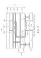
- FIG. 14is a cross-sectional view of a circuit device according to a fifth exemplary embodiment of the present invention.
- FIG. 15is a cross-sectional view of a circuit device according to a sixth exemplary embodiment of the present invention.
- FIG. 16is a cross-sectional view of a circuit device according to a seventh exemplary embodiment of the present invention.
- FIG. 17is a cross-sectional view of a circuit device according to an eighth exemplary embodiment of the present invention.
- FIG. 18is a cross-sectional view of a circuit device according to a ninth exemplary embodiment of the present invention.
- FIG. 19is a diagram illustrating a circuit device attached to a printed circuit board.
- FIG. 20is a cross-sectional view of a circuit device according to a tenth exemplary embodiment of the present invention.
- FIG. 21is a diagram illustrating an exemplary 4-element phased array which uses a proposed signal line transition design to couple a semiconductor die and four antennas.
- the conception of the present inventionis to provide a multilayer signal line transition design, such as a multilayer vertical transition design for transmitting signals with frequencies within or above the millimeter wave (mmWave) range.
- an exemplary embodiment of the present inventionproposes a circuit device with a signal line transition element which passes signals through multiple layers (e.g., substrate layers) of a multilayer circuit carrier and has two signal terminals respectively electrically connected to impedance transformers.
- a low-cost circuit devicee.g., a low-cost package
- the proposed circuit deviceis consistent with the printed circuit board (PCB) manufacturing process or the low temperature co-fired ceramics (LTCC) manufacturing process, etc. Further details of the proposed circuit device will be described as follows.
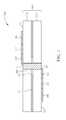
- FIG. 1is a cross-sectional view of a circuit device according to a first exemplary embodiment of the present invention.
- FIG. 2is a top view of the exemplary circuit device shown in FIG. 1 .
- the exemplary circuit device 100includes, but is not limited to, a multilayer circuit carrier 102 , a first signal transmission line 104 , a second signal transmission line 106 , a signal line transition element 108 , a first impedance transformer 110 , and a second impedance transformer 112 .
- the multilayer circuit carrier 102has a plurality of layers including a first layer 114 and a second layer 116 . It should be noted that only two layers are shown in FIG.
- the first signal transmission line 104has impedance such as 50 Ohms, and is disposed on a surface Si of the first layer 114 .
- the second signal transmission line 106has impedance such as 50 Ohms, and disposed on a surface S 2 of the second layer 116 .
- the signal line transition element 108passes through at least the first layer 114 and the second layer 116 included in the multilayer circuit carrier 102 , and has a first signal terminal Ti on the first layer 114 and a second signal terminal T 2 on the second layer 116 .
- the signal line transition element 108may be implemented by an electrically conductive element (e.g., a signal via) passing through the first layer 114 and the second layer 116 in a thickness direction of the multilayer circuit carrier 102 .
- a signal viamay be formed by any available process.
- the signal viamay be realized by a plated hole without any metal material filled therein.
- the signal viamay be realized by a hole filled with a metal material (e.g., Ag, Cu, or Au).
- a metal materiale.g., Ag, Cu, or Au
- the first impedance transformer 110is disposed on the surface S 1 of the first layer 114 and electrically connected between the first signal transmission line 104 and the first signal terminal T 1 of the signal line transition element 108 , and implemented for providing impedance matching between the first signal transmission line 104 and the signal line transition element 108 .
- the second impedance transformer 112is disposed on the surface S 2 of the second layer 116 and electrically connected between the second signal transmission line 106 and the second signal terminal T 2 of the signal line transition element 108 , and implemented for providing impedance matching between the second signal transmission line 106 and the signal line transition element 108 .
- the first impedance transformer 110 and the second impedance transformer 112are therefore used for acting as impedance matching networks to make the antenna feed impedance, typically 50 Ohms, not change through the non-ideal signal line transition element 108 .
- the signal transmission performanceis improved by reducing undesired signal loss.
- the angle ⁇ between the first signal transmission line 104 and the second signal transmission line 106is arbitrary.
- the signal line transitioncan be designed in a systematic way and the signal routing layout is very flexible, which can easily meet the requirements of any application.
- each short line segmentthere are one optional short line segment 118 electrically connected between the first impedance transformer 110 and the signal line transition element 108 and another optional short line segment 120 electrically connected between the second impedance transformer 112 and the signal line transition element 108 .
- the line length of each short line segmentcan be adjusted so that the line impedance viewed at the impedance transformer is purely real.
- the short line segments 118 and 120 each having a variable lengthmay be omitted. Therefore, the first impedance transformer 110 may be directly connected to the first signal terminal T 1 of the signal line transition element 108 , and the second impedance transformer 112 may be directly connected to the second signal terminal T 2 of the signal line transition element 108 .
- the first signal transmission line 104 , the first impedance transformer 110 , and the optional short line segment 118may be routed on one metal layer on the surface S 1 of the first layer 114
- the second signal transmission line 106 , the second impedance transformer 112 , and the optional short line segment 120may be routed on another metal layer on the surface S 2 of the second layer 116 .
- an additional metal layercan be added to reduce the crowdedness of input/output pads formed on the surface S 2 , thereby simplifying the interface design between the circuit device 100 and a semiconductor die to be mounted onto the circuit device 100 .
- the electromagnetic shielding techniquemay be employed.
- the signal line transition element 108may be implemented by a coaxial-like transmission line, and/or the signal line transition element 108 passes through at least one reference voltage plane which is disposed on one of the layers included in the multilayer circuit carrier 102 and arranged to deliver a predetermined reference voltage such as a power supply voltage or a ground voltage.
- any physical signal conveyance elemente.g., a signal via of the signal line transition element 108 is isolated from the reference voltage plane(s) when passing through the reference voltage plane(s).
- a reference voltage plane 111may be formed between the first layer 114 and the second layer 116 .
- an area surrounding the signal line transition element 108is free of the conductive plane material and therefore serves as an anti-pad 109 . It should be noted that using the signal line transition element 108 to pass signals through the reference voltage plane 111 is for illustrative purposes only, and is not meant to be a limitation of the present invention.
- the coaxial-like transmission linehas an inner conductor surrounded by a conductive shielding structure.
- a conductive shielding structureIn this way, when the proposed circuit device is employed in a high-frequency application (e.g., a mmWave application), the signal loss due to undesired radiation can be avoided/reduced by the conductive shielding structure.
- the reference voltage planesuch as a power plane or a ground plane, is DC-shorted under a high-frequency operational environment, the signal loss due to the undesired radiation may be reduced by the reference voltage plane, too.
- the proposed multilayer signal line transition designhas very good performance, almost independent of the layer thickness.
- FIG. 3is a cross-sectional view of a circuit device according to a second exemplary embodiment of the present invention.
- FIG. 4is a top view of the exemplary circuit device shown in FIG. 3 .
- the circuit device 200has the similar structure shown in FIG. 1 and additional elements implemented therein.
- the multilayer circuit carrier 202includes the first layer 114 , the second layer 116 , and a third layer 204 above the first layer 114 . It should be noted that only three layers are shown here for illustrative purposes only.
- one reference voltage plane 206is disposed on the third layer 204 and arranged to deliver a predetermined reference voltage
- another reference voltage plane 208is disposed between the first layer 114 and the second layer 116 , and is arranged to deliver a predetermined reference voltage.
- the reference voltage plane 206may be an antenna ground plane of an antenna (not shown)
- the reference voltage plane 208may be a ground plane of a semiconductor die or other circuitry (not shown).
- the signal line transition element 214is a coaxial-like transmission line realized by a signal via 212 and a plurality of shielding vias 210 disposed around the signal via 212 . It should be noted that the shielding via may be formed by any available process.
- the shielding viamay be realized by a plated hole without any stuff filled therein.
- the shielding viamay be realized by a hole filled with a metal material (e.g., Ag, Cu, or Au).
- a metal materiale.g. Ag, Cu, or Au.
- each of the shielding vias 210is connected between the reference voltage planes 206 and 208 and utilized for transmitting a predetermined reference voltage.
- each shielding via 210acts as a grounded via.
- FIG. 5is a top view illustrating the signal via 212 passing through a ground plane 502 such as the reference voltage planes 208 in FIG. 3 .
- any physical signal conveyance elemente.g., a signal via of the signal line transition element is isolated from the reference voltage plane(s) when passing through the reference voltage plane(s). Therefore, as can be seen from FIG. 3 , the signal via 212 is not electrically connected to the ground plane 502 when passing through the ground plane 502 .
- the reference voltage planeis DC-shorted under the high-frequency operational environment.
- the reference voltage plane 208may also be a power plane.
- FIG. 6is a top view illustrating the signal via 212 passing through a power plane 602 such as the reference voltage planes 208 shown in FIG. 3 .
- a reflector 604 for reducing the back radiationmay be disposed at an internal cut area of the power plane 602 .
- thisis for illustrative purposes only.
- the reflector 604may be removed from the internal area of the power plane 602 , and placed on another layer of the multilayer circuit carrier 202 (e.g., disposed between the power plane 602 and the first signal transmission line 104 which acts as an antenna feed line).
- the reflector 604may be removed from the internal area of the power plane 602 , and the power plane 602 itself functions as the reflector for the antenna to reduce the back radiation.
- any physical signal conveyance elemente.g., a signal via
- the signal via 212is not electrically connected to the power plane 602 when passing through the power plane 602 .
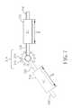
- At least one of the first impedance transformer 110 and the second impedance transformer 112may be implemented by a quarter wavelength transformer. Taking the circuit device 200 shown in FIG. 3 for example, the first impedance transformer 110 and the second impedance transformer 112 respectively implemented by quarter wavelength transformers 710 and 712 are shown in FIG. 7 .
- Each of the first signal transmission line 104 and the second signal transmission line 106has impedance Z S .
- the impedance Z Sis purely real impedance R S , such as 50 Ohms. If the impedance of the signal line transition element 214 is a complex value, the length of the short line segment 118 may be properly set to convert the complex input impedance into purely real impedance R L viewed by the quarter wavelength transformer 710 .
- the impedance of the signal line transition element 214is the purely real impedance R L , the short line segment 118 can be omitted.
- the impedance Z 0 of the quarter wavelength transformer 710can be simply determined according to the following equation.
- the line length of the quarter wavelength transformer 710is equal to
- ⁇is the wavelength of a transmitted sinusoidal signal (e.g., an RF signal), and can be easily determined according to the following equation.
- V in above equation (2)represents the phase velocity (i.e., speed of light/ ⁇ square root over ( ⁇ ) ⁇ , 3 ⁇ 10 8 , ⁇ square root over ( ⁇ ,) ⁇ m/s), and f in above equation (2) represents the frequency of the sinusoidal signal to be transmitted.
- the covered frequency range of the RF signalmay be from 57 GHz to 66 GHz. Therefore, the line length of the quarter wavelength transformer 710 may be determined according to a middle value (i.e., 61.5 GHz) of the covered frequency range.
- the implementation of the aforementioned impedance transformeris not limited to a quarter wavelength transformer.
- at least one of the first impedance transformer 110 and the second impedance transformer 112may be implemented by a multi-stub matching network (e.g., a double-stub matching network) with a plurality of open-circuited stubs or a single-stub matching network with an open-circuited stub. Taking the circuit device 200 shown in FIG.
- the first impedance transformer 110 and the second impedance transformer 112 respectively implemented by single-stub matching networks 910 and 912 each having one open-circuited stub 911 / 913are shown in FIG. 9 .
- the same objective of providing the required impedance matching between the first signal transmission line 104 /second signal transmission line 106 and the signal line transition element 214is achieved.
- FIG. 10is a cross-sectional view of a circuit device according to a third exemplary embodiment of the present invention.
- FIG. 11is a top view of the exemplary circuit device shown in FIG. 10 .
- FIG. 12is a cross-sectional view of a circuit device according to a fourth exemplary embodiment of the present invention.
- FIG. 13is a top view of the exemplary circuit device shown in FIG. 12 .
- the major difference between the exemplary circuit device 300 in FIG. 10 and the exemplary circuit device 200 in FIG. 3is that the first impedance transformer 110 is further electrically connected to the first reference voltage plane (e.g., a ground plane) 206 through short-circuited vias 302 _A and 302 _B, and the second impedance transformer 112 is further electrically connected to the second reference voltage plane (e.g., a ground plane) 208 through short-circuited vias 304 _A and 304 _B.
- first impedance transformer 110is further electrically connected to the first reference voltage plane (e.g., a ground plane) 206 through a short-circuited via 402
- second impedance transformer 112is further electrically connected to the second reference voltage plane (e.g., a ground plane) 208 through a short-circuited via 404 .
- the aforementioned first impedance transformer 110 and the second impedance transformer 112 respectively implemented by double-stub matching networks 1110 and 1112 each having two short-circuited stubs 1111 _A and 1111 _B/ 1113 _A and 1113 _Bare shown in FIG. 11
- the aforementioned first impedance transformer 110 and the second impedance transformer 112 respectively implemented by single-stub matching networks 1310 and 1312 each having one short-circuited stub 1311 / 1313are shown in FIG. 13 .
- the same objective of providing the required impedance matching between the first signal transmission line 104 /second signal transmission line 106 and the signal line transition element 214is achieved.
- the exemplary impedance transformer implementationmay also be employed to realize at least one of the first impedance transformer 110 and the second impedance transformer 112 included in the circuit device 100 shown in FIG. 1 . This also falls within the scope of the present invention.
- Each of the exemplary circuit devices proposed abovemay have antenna(s) and/or semiconductor die(s) integrated therein. Therefore, the aforementioned first signal transmission line 104 may serve as an antenna feed line, and the aforementioned second signal transmission line 106 may be used to connect a mounted semiconductor die with an RF signal processing capability.
- the exemplary circuit device of the present inventionis suitable for a high-frequency application due to the particularly designed multilayer signal line transition design.
- some exemplary circuit devices each having an integrated antenna included thereinare provided.
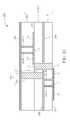
- FIG. 14is a cross-sectional view of a circuit device according to a fifth exemplary embodiment of the present invention.
- the exemplary circuit device 1400includes, but is not limited to, a multilayer circuit carrier 1406 including a plurality of layers 1401 - 1405 , a first signal transmission line 1407 acting as an antenna feed line, a second signal transmission line 1408 , a signal line transition element 1411 including a signal via 1409 and a plurality of shielding vias 1410 , a first impedance transformer 1412 , a second impedance transformer 1413 , a semiconductor die (e.g., an RF die with at least the RF signal processing capability) 1414 , a patch antenna 1417 including a patch 1415 and an antenna ground plane 1416 , and a power plane 1418 with/without a reflector formed on the same layer.
- a semiconductor diee.g., an RF die with at least the RF signal processing capability
- the second signal transmission line 1408 and the semiconductor die 1414are mounted on the same surface of the layer 1401 .
- the semiconductor die 1414is electrically connected to the second signal transmission line 1408 for transmitting or receiving signals (e.g., RF signals) between the multilayer circuit carrier 1406 and the semiconductor die 1414 .
- the semiconductor die 1414is mounted onto the layer 1401 through a flip-chip bonding manner.
- the patch antenna 1417is an aperture-coupled patch antenna.
- the antenna ground plane 1416 disposed between the patch 1415 and the antenna feed linei.e., the first signal transmission line 1407
- the patch 1415is accommodated in an internal cavity (e.g., an air cavity) of the multilayer circuit carrier 1406 for achieving better antenna performance.
- FIG. 15is a cross-sectional view of a circuit device according to a sixth exemplary embodiment of the present invention.
- the exemplary circuit device 1500has a multilayer circuit carrier 1505 including a plurality of layers 1501 - 1504 .
- no internal cavity for accommodating a patch 1515 of a patch antenna 1517is formed in the multilayer circuit carrier 1505 . Therefore, the production cost can be reduced since no internal cavity is needed.
- FIG. 16is a cross-sectional view of a circuit device according to a seventh exemplary embodiment of the present invention.
- the exemplary circuit device 1600has a multilayer circuit carrier 1604 including a plurality of layers 1601 - 1603 .
- the first signal transmission line 1407 and a patch 1616 of a patch antenna 1617are both disposed on the same surface of the layer 1603 .
- the first signal transmission line 1407acts as an antenna feed line, and is directly connected to an edge of the patch 1616 .
- an antenna ground plane 1615 of the patch antenna 1617is disposed below the patch 1616 without any aperture formed therein.
- FIG. 17is a cross-sectional view of a circuit device according to an eighth exemplary embodiment of the present invention.
- the exemplary circuit device 1700has a multilayer circuit carrier 1704 including a plurality of layers 1701 - 1703 .
- a slot antenna 1717is formed on the surface of the layer 1703 , where the slot antenna 1717 has a slot 1715 which is formed in an antenna ground plane 1716 of the slot antenna 1717 and serves as a radiating element.
- FIG. 18is a cross-sectional view of a circuit device according to a ninth exemplary embodiment of the present invention.
- the exemplary circuit device 1800has a multilayer circuit carrier 1807 including a plurality of layers 1801 - 1806 .
- the aforementioned aperture-coupled patch antenna 1517is integrated with the multilayer circuit carrier 1807 .
- another antenna structuremay be used. In this exemplary embodiment shown in FIG.
- a power plane 1808is disposed between the layers 1801 and 1802
- a reflector (or other circuitry) 1809is disposed between layers 1803 and 1804
- the semiconductor die 1414is accommodated in an open cavity 1810 of the multilayer circuit carrier 1807 and may be mounted onto the layer 1803 through a flip-chip bonding manner.
- the proposed circuit device with antenna(s) and/or semiconductor die(s) carried thereonmay be further attached to a printed circuit board (PCB).
- PCBprinted circuit board
- a surface-mount packaging techniquesuch as a ball grid array (BGA)
- BGAball grid array
- FIG. 19is a diagram illustrating the circuit device 1400 attached to a PCB 1902 . If the heat dissipation is an issue to be solved, a heat sink 1904 may be used. However, implementing a heat dissipater inside the proposed circuit device is also feasible.
- FIG. 20is a cross-sectional view of a circuit device according to a tenth exemplary embodiment of the present invention.
- the exemplary circuit device 2000has a multilayer circuit carrier 2008 including a plurality of layers 2001 - 2007 .
- the circuit device 2000is based on the circuit device 1400 shown in FIG. 14 , and further has a heat dissipater 2011 integrated in the multilayer circuit carrier 2008 .
- the heat dissipater 2011includes at least one heat dissipation via 2009 and at least one heat dissipation plane (e.g., a ground plane) 2010 .
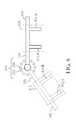
- FIG. 21is a diagram illustrating an exemplary 4-element phased array (antenna array) which uses the aforementioned multilayer signal line transition design to couple a semiconductor die and four antennas.
- this 4-element phased array (antenna array) realized by the exemplary circuit device 2100four patch antennas are used. Therefore, four patches 2104 _ 1 - 2104 _ 4 are mounted on a multilayer circuit carrier (e.g., one of the aforementioned multilayer circuit carriers) to which a semiconductor die 2102 with at least the RF signal processing capability is attached.
- a multilayer circuit carriere.g., one of the aforementioned multilayer circuit carriers
- First signal transmission lines (i.e., antenna feed lines) 2106 _ 1 - 2106 _ 4are coupled to respective patches 2104 _ 1 - 2104 _ 4 , and also electrically connected to the semiconductor die 2102 through respective first impedance transformers 2105 _ 1 - 2105 _ 4 , respective signal vias 2108 _ 1 - 2108 _ 4 each passing through multiple layers of the multilayer circuit carrier, respective second impedance transformers 2107 _ 1 - 2107 _ 4 , and respective second transmission lines 2110 _ 1 - 2110 _ 4 .
- shielding vias 2109may be implemented to avoid the unwanted coupling and reduce the undesired signal loss.
- the signal routing design between the patch 2104 _ 1 and the semiconductor die 2102 and the signal routing design between the patch 2104 _ 2 and the semiconductor die 2102are symmetrical; in addition, the signal routing design between the patch 2104 _ 3 and the semiconductor die 2102 and the signal routing design between the patch 2104 _ 4 and the semiconductor die 2102 are also symmetrical.
- thisis for illustrative purposes only. That is, the signal routing designs for the patches 2104 _ 1 - 2104 _ 4 may be the same or different, depending upon the actual design consideration.
- the proposed multilayer signal line transition designis applicable to a rectangular antenna array, a circular antenna array, a triangular antenna array, etc.
Landscapes
- Variable-Direction Aerials And Aerial Arrays (AREA)
- Semiconductor Integrated Circuits (AREA)
- Structure Of Printed Boards (AREA)
- Waveguides (AREA)
- Waveguide Aerials (AREA)
- Details Of Aerials (AREA)
Abstract
Description
- The disclosed embodiments of the present invention relate to transmitting high-frequency signals, and more particularly, to a circuit device with a signal line transition element which passes signals through multiple layers of a multilayer circuit carrier and with impedance transformers electrically connected to signal terminals of the signal line transition element.
- In a wireless network, the connectivity and communication between devices is achieved through antennas attached to receivers or transmitters in order to radiate the desired signals to or receive the desired signals from other elements of the wireless network. In radio communication systems, such as millimeter-wave radios, discrete components are usually assembled with low integration levels. These systems are often assembled using expensive and bulky waveguides and package-level or board-level microstrip structures to interconnect semiconductor elements and their required transmitter/receiver antennas. With recent progress in the semiconductor technology and packaging engineering, the dimensions of these radio communication systems become smaller and the integration of antennas with their radio-frequency (RF) front-end circuits becomes more desirable. For a specific application such as a wireless universal serial bus (USB) application, the operating distance is limited to about one meter, and a single antenna with about 7 dBi at 60 GHz will provide the necessary antenna gain. For one point-to-point application (such as a wireless video application) which has an operating distance as long as 10 meters or another point-to-point application (such as a radar application) which has an operating distance longer than 10 meters, an antenna gain as high as 30 dBi, depending on the actual application, is required. However, a high gain antenna generally has a very narrow beam width, so pointing the antenna is very difficult for consumers. Therefore, a radiation pattern steerable array (also called phased array) is necessary. For example, phased arrays are widely used in military radars. However, packaging an RF die with an integrated antenna or antenna array is extremely difficult and very expensive due to expensive components and extensive labor involved.
- Thus, there is a need for an innovative assembly design of wireless communication elements.
- In accordance with exemplary embodiments of the present invention, a circuit device with a signal line transition element (e.g., signal via) which passes high-frequency signals through multiple layers of a multilayer circuit carrier (e.g., a package having an integrated antenna or antenna array) and impedance transformers electrically connected to signal terminals of the signal line transition element is proposed.
- According to an aspect of the present invention, an exemplary circuit device is proposed. The exemplary circuit device includes a multilayer circuit carrier, a first signal transmission line, a second signal transmission line, a signal line transition element, a first impedance transformer, and a second impedance transformer. The multilayer circuit carrier has a plurality of layers including a first layer and a second layer. The first signal transmission line is disposed on the surface of the first layer. The second signal transmission line is disposed on the surface of the second layer. The signal line transition element passes through at least the first layer and the second layer, and has a first signal terminal on the first layer and a second signal terminal on the second layer. The first impedance transformer is disposed on the surface of the first layer and electrically connected between the first signal transmission line and the first signal terminal, for providing impedance matching between the first signal transmission line and the signal line transition element. The second impedance transformer is disposed on the surface of the second layer and electrically connected between the second signal transmission line and the second signal terminal, for providing impedance matching between the second signal transmission line and the signal line transition element.
- These and other objectives of the present invention will no doubt become obvious to those of ordinary skill in the art after reading the following detailed description of the preferred embodiment that is illustrated in the various figures and drawings.
FIG. 1 is a cross-sectional view of a circuit device according to a first exemplary embodiment of the present invention.FIG. 2 is a top view of the exemplary circuit device shown inFIG. 1 .FIG. 3 is a cross-sectional view of a circuit device according to a second exemplary embodiment of the present invention.FIG. 4 is a top view of the exemplary circuit device shown inFIG. 3 .FIG. 5 is a top view illustrating a signal via passing through a ground plane.FIG. 6 is a top view illustrating a signal via passing through a power plane.FIG. 7 is a diagram illustrating impedance transformers implemented by quarter wavelength transformers.FIG. 8 is a diagram illustrating impedance transformers implemented by double-stub matching networks each having two open-circuited stubs.FIG. 9 is a diagram illustrating impedance transformers implemented by single-stub matching networks each having one open-circuited stub.FIG. 10 is a cross-sectional view of a circuit device according to a third exemplary embodiment of the present invention.FIG. 11 is a top view of the exemplary circuit device shown inFIG. 10 .FIG. 12 is a cross-sectional view of a circuit device according to a fourth exemplary embodiment of the present invention.FIG. 13 is a top view of the exemplary circuit device shown inFIG. 12 .FIG. 14 is a cross-sectional view of a circuit device according to a fifth exemplary embodiment of the present invention.FIG. 15 is a cross-sectional view of a circuit device according to a sixth exemplary embodiment of the present invention.FIG. 16 is a cross-sectional view of a circuit device according to a seventh exemplary embodiment of the present invention.FIG. 17 is a cross-sectional view of a circuit device according to an eighth exemplary embodiment of the present invention.FIG. 18 is a cross-sectional view of a circuit device according to a ninth exemplary embodiment of the present invention.FIG. 19 is a diagram illustrating a circuit device attached to a printed circuit board.FIG. 20 is a cross-sectional view of a circuit device according to a tenth exemplary embodiment of the present invention.FIG. 21 is a diagram illustrating an exemplary 4-element phased array which uses a proposed signal line transition design to couple a semiconductor die and four antennas.- Certain terms are used throughout the description and following claims to refer to particular components. As one skilled in the art will appreciate, manufacturers may refer to a component by different names. This document does not intend to distinguish between components that differ in name but not function. In the following description and in the claims, the terms “include” and “comprise” are used in an open-ended fashion, and thus should be interpreted to mean “include, but not limited to . . . ”. Also, the term “electrically connected” is intended to mean either an indirect or direct electrical connection. Accordingly, if one device is electrically connected to another device, that connection may be through a direct electrical connection, or through an indirect electrical connection via other devices and connections.
- The conception of the present invention is to provide a multilayer signal line transition design, such as a multilayer vertical transition design for transmitting signals with frequencies within or above the millimeter wave (mmWave) range. For example, an exemplary embodiment of the present invention proposes a circuit device with a signal line transition element which passes signals through multiple layers (e.g., substrate layers) of a multilayer circuit carrier and has two signal terminals respectively electrically connected to impedance transformers. In this way, a low-cost circuit device (e.g., a low-cost package) with integrated antenna(s) and/or semiconductor die(s) may be realized with a minimal impact on the antenna performance. In addition, the proposed circuit device is consistent with the printed circuit board (PCB) manufacturing process or the low temperature co-fired ceramics (LTCC) manufacturing process, etc. Further details of the proposed circuit device will be described as follows.
- Please refer to
FIG. 1 in conjunction withFIG. 2 .FIG. 1 is a cross-sectional view of a circuit device according to a first exemplary embodiment of the present invention.FIG. 2 is a top view of the exemplary circuit device shown inFIG. 1 . Theexemplary circuit device 100 includes, but is not limited to, amultilayer circuit carrier 102, a firstsignal transmission line 104, a secondsignal transmission line 106, a signalline transition element 108, afirst impedance transformer 110, and asecond impedance transformer 112. Themultilayer circuit carrier 102 has a plurality of layers including afirst layer 114 and asecond layer 116. It should be noted that only two layers are shown inFIG. 1 for illustrative purposes only, and the total number of layers included in themultilayer circuit carrier 102 depends upon the actual design consideration. The firstsignal transmission line 104 has impedance such as 50 Ohms, and is disposed on a surface Si of thefirst layer 114. The secondsignal transmission line 106 has impedance such as 50 Ohms, and disposed on a surface S2 of thesecond layer 116. The signalline transition element 108 passes through at least thefirst layer 114 and thesecond layer 116 included in themultilayer circuit carrier 102, and has a first signal terminal Ti on thefirst layer 114 and a second signal terminal T2 on thesecond layer 116. For example, the signalline transition element 108 may be implemented by an electrically conductive element (e.g., a signal via) passing through thefirst layer 114 and thesecond layer 116 in a thickness direction of themultilayer circuit carrier 102. It should be noted that the signal via may be formed by any available process. For example, if the PCB manufacturing process is employed, the signal via may be realized by a plated hole without any metal material filled therein. However, if the LTCC manufacturing process is employed, the signal via may be realized by a hole filled with a metal material (e.g., Ag, Cu, or Au). To put it simply, provided that the objective of providing vertical signal transmission is achieved, any via structure may be employed to realize the desired signal via. Thefirst impedance transformer 110 is disposed on the surface S1 of thefirst layer 114 and electrically connected between the firstsignal transmission line 104 and the first signal terminal T1 of the signalline transition element 108, and implemented for providing impedance matching between the firstsignal transmission line 104 and the signalline transition element 108. Thesecond impedance transformer 112 is disposed on the surface S2 of thesecond layer 116 and electrically connected between the secondsignal transmission line 106 and the second signal terminal T2 of the signalline transition element 108, and implemented for providing impedance matching between the secondsignal transmission line 106 and the signalline transition element 108. - As the signal
line transition element 108 may not have the desired impedance (e.g., 50 Ohms), thefirst impedance transformer 110 and thesecond impedance transformer 112 are therefore used for acting as impedance matching networks to make the antenna feed impedance, typically 50 Ohms, not change through the non-ideal signalline transition element 108. In this way, the signal transmission performance is improved by reducing undesired signal loss. In addition, as the firstsignal transmission line 104 and the secondsignal transmission line 106 are disposed on different layers, respectively, the angle θ between the firstsignal transmission line 104 and the secondsignal transmission line 106 is arbitrary. Thus, the signal line transition can be designed in a systematic way and the signal routing layout is very flexible, which can easily meet the requirements of any application. - It should be noted that there are one optional
short line segment 118 electrically connected between thefirst impedance transformer 110 and the signalline transition element 108 and another optionalshort line segment 120 electrically connected between thesecond impedance transformer 112 and the signalline transition element 108. The line length of each short line segment can be adjusted so that the line impedance viewed at the impedance transformer is purely real. However, in an alternative design, theshort line segments first impedance transformer 110 may be directly connected to the first signal terminal T1 of the signalline transition element 108, and thesecond impedance transformer 112 may be directly connected to the second signal terminal T2 of the signalline transition element 108. - The first
signal transmission line 104, thefirst impedance transformer 110, and the optionalshort line segment 118 may be routed on one metal layer on the surface S1 of thefirst layer 114, and the secondsignal transmission line 106, thesecond impedance transformer 112, and the optionalshort line segment 120 may be routed on another metal layer on the surface S2 of thesecond layer 116. However, it is possible to replace thefirst layer 114 with more layers for allowing more functions to be realized by using thecircuit device 100. Besides, it is also possible to replace thesecond layer 116 with more layers or different materials. For example, an additional metal layer can be added to reduce the crowdedness of input/output pads formed on the surface S2, thereby simplifying the interface design between thecircuit device 100 and a semiconductor die to be mounted onto thecircuit device 100. - To further reduce undesired signal loss for improving the signal transmission performance, the electromagnetic shielding technique may be employed. For example, the signal
line transition element 108 may be implemented by a coaxial-like transmission line, and/or the signalline transition element 108 passes through at least one reference voltage plane which is disposed on one of the layers included in themultilayer circuit carrier 102 and arranged to deliver a predetermined reference voltage such as a power supply voltage or a ground voltage. As the signalline transition element 108 is intended for signal conveyance, any physical signal conveyance element (e.g., a signal via) of the signalline transition element 108 is isolated from the reference voltage plane(s) when passing through the reference voltage plane(s). For example, areference voltage plane 111 may be formed between thefirst layer 114 and thesecond layer 116. In this exemplary embodiment, an area surrounding the signalline transition element 108 is free of the conductive plane material and therefore serves as an anti-pad109. It should be noted that using the signalline transition element 108 to pass signals through thereference voltage plane 111 is for illustrative purposes only, and is not meant to be a limitation of the present invention. - The coaxial-like transmission line has an inner conductor surrounded by a conductive shielding structure. In this way, when the proposed circuit device is employed in a high-frequency application (e.g., a mmWave application), the signal loss due to undesired radiation can be avoided/reduced by the conductive shielding structure. Similarly, as the reference voltage plane, such as a power plane or a ground plane, is DC-shorted under a high-frequency operational environment, the signal loss due to the undesired radiation may be reduced by the reference voltage plane, too. To put it simply, when the coaxial-like transmission line which provides an outside shield is employed, the proposed multilayer signal line transition design has very good performance, almost independent of the layer thickness.
- Please refer to
FIG. 3 in conjunction withFIG. 4 .FIG. 3 is a cross-sectional view of a circuit device according to a second exemplary embodiment of the present invention.FIG. 4 is a top view of the exemplary circuit device shown inFIG. 3 . Thecircuit device 200 has the similar structure shown inFIG. 1 and additional elements implemented therein. In this exemplary embodiment, themultilayer circuit carrier 202 includes thefirst layer 114, thesecond layer 116, and athird layer 204 above thefirst layer 114. It should be noted that only three layers are shown here for illustrative purposes only. In addition, onereference voltage plane 206 is disposed on thethird layer 204 and arranged to deliver a predetermined reference voltage, and anotherreference voltage plane 208 is disposed between thefirst layer 114 and thesecond layer 116, and is arranged to deliver a predetermined reference voltage. By way of example, but not limitation, thereference voltage plane 206 may be an antenna ground plane of an antenna (not shown), and thereference voltage plane 208 may be a ground plane of a semiconductor die or other circuitry (not shown). Moreover, the signalline transition element 214 is a coaxial-like transmission line realized by a signal via212 and a plurality of shieldingvias 210 disposed around the signal via212. It should be noted that the shielding via may be formed by any available process. For example, if the PCB manufacturing process is employed, the shielding via may be realized by a plated hole without any stuff filled therein. However, if the LTCC manufacturing process is employed, the shielding via may be realized by a hole filled with a metal material (e.g., Ag, Cu, or Au). To put it simply, provided that the objective of shielding the signal via is achieved, any via structure may be employed to realize the desired shielding via. As shown inFIG. 3 , the signal via212 passes through at least thefirst layer 114 and thesecond layer 116 in the thickness direction of themultilayer circuit carrier 202. In other words, the signal via212 provides a vertical transmission path. In addition, as can be seen fromFIG. 3 , two ends of the signal via212 serve as the first signal terminal T1 and the second signal terminal T2 of the signalline transition element 214, respectively. Each of the shieldingvias 210 is connected between thereference voltage planes reference voltage planes FIG. 5 , which is a top view illustrating the signal via212 passing through aground plane 502 such as thereference voltage planes 208 inFIG. 3 . As mentioned above, any physical signal conveyance element (e.g., a signal via) of the signal line transition element is isolated from the reference voltage plane(s) when passing through the reference voltage plane(s). Therefore, as can be seen fromFIG. 3 , the signal via212 is not electrically connected to theground plane 502 when passing through theground plane 502. - It should be noted that the reference voltage plane, either a ground plane or a power plane, is DC-shorted under the high-frequency operational environment. Thus, regarding a high-frequency application, the
reference voltage plane 208 may also be a power plane. Please refer toFIG. 6 , which is a top view illustrating the signal via212 passing through apower plane 602 such as thereference voltage planes 208 shown inFIG. 3 . In a case where thecircuit device 200 shown inFIG. 3 is employed to carry an antenna (not shown) of the high-frequency application, areflector 604 for reducing the back radiation may be disposed at an internal cut area of thepower plane 602. However, this is for illustrative purposes only. In an alternative design, thereflector 604 may be removed from the internal area of thepower plane 602, and placed on another layer of the multilayer circuit carrier202 (e.g., disposed between thepower plane 602 and the firstsignal transmission line 104 which acts as an antenna feed line). Alternatively, thereflector 604 may be removed from the internal area of thepower plane 602, and thepower plane 602 itself functions as the reflector for the antenna to reduce the back radiation. As mentioned above, any physical signal conveyance element (e.g., a signal via) of the signal line transition element is isolated from the reference voltage plane(s) when passing through the reference voltage plane(s). Therefore, as can be seen fromFIG. 6 , the signal via212 is not electrically connected to thepower plane 602 when passing through thepower plane 602. - At least one of the
first impedance transformer 110 and thesecond impedance transformer 112 may be implemented by a quarter wavelength transformer. Taking thecircuit device 200 shown inFIG. 3 for example, thefirst impedance transformer 110 and thesecond impedance transformer 112 respectively implemented byquarter wavelength transformers FIG. 7 . Each of the firstsignal transmission line 104 and the secondsignal transmission line 106 has impedance ZS. For example, the impedance ZSis purely real impedance RS, such as 50 Ohms. If the impedance of the signalline transition element 214 is a complex value, the length of theshort line segment 118 may be properly set to convert the complex input impedance into purely real impedance RLviewed by thequarter wavelength transformer 710. However, if the impedance of the signalline transition element 214 is the purely real impedance RL, theshort line segment 118 can be omitted. The impedance Z0of thequarter wavelength transformer 710 can be simply determined according to the following equation.
Z0=√{square root over (RS·RL)} (1)- In addition, the line length of the
quarter wavelength transformer 710 is equal to - where λ is the wavelength of a transmitted sinusoidal signal (e.g., an RF signal), and can be easily determined according to the following equation.
- Regarding the transmission of the sinusoidal signal, V in above equation (2) represents the phase velocity (i.e., speed of light/√{square root over (ε)}, 3×10⁸, √{square root over (ε,)} m/s), and f in above equation (2) represents the frequency of the sinusoidal signal to be transmitted. For example, regarding a mmWave application, the covered frequency range of the RF signal may be from 57 GHz to 66 GHz. Therefore, the line length of the
quarter wavelength transformer 710 may be determined according to a middle value (i.e., 61.5 GHz) of the covered frequency range. - As a person skilled in the art can readily understand how to determine the impedance Z0′ (Z0′ may be identical to or different from Z0) and the line length
- of the other
quarter wavelength transformer 712, further description is omitted here for brevity. - It should be noted that the implementation of the aforementioned impedance transformer is not limited to a quarter wavelength transformer. For example, in one alternative design, at least one of the
first impedance transformer 110 and thesecond impedance transformer 112 may be implemented by a multi-stub matching network (e.g., a double-stub matching network) with a plurality of open-circuited stubs or a single-stub matching network with an open-circuited stub. Taking thecircuit device 200 shown inFIG. 3 for example, thefirst impedance transformer 110 and thesecond impedance transformer 112 respectively implemented by double-stub matching networks FIG. 8 , and thefirst impedance transformer 110 and thesecond impedance transformer 112 respectively implemented by single-stub matching networks stub 911/913 are shown inFIG. 9 . The same objective of providing the required impedance matching between the firstsignal transmission line 104/secondsignal transmission line 106 and the signalline transition element 214 is achieved. - In another alternative design, at least one of the
first impedance transformer 110 and thesecond impedance transformer 112 may be implemented by a multi-stub matching network (e.g., a double-stub matching network) with a plurality of short-circuited stubs or a single-stub matching network with a short-circuited stub.FIG. 10 is a cross-sectional view of a circuit device according to a third exemplary embodiment of the present invention.FIG. 11 is a top view of the exemplary circuit device shown inFIG. 10 .FIG. 12 is a cross-sectional view of a circuit device according to a fourth exemplary embodiment of the present invention.FIG. 13 is a top view of the exemplary circuit device shown inFIG. 12 . The major difference between theexemplary circuit device 300 inFIG. 10 and theexemplary circuit device 200 inFIG. 3 is that thefirst impedance transformer 110 is further electrically connected to the first reference voltage plane (e.g., a ground plane)206 through short-circuited vias302_A and302_B, and thesecond impedance transformer 112 is further electrically connected to the second reference voltage plane (e.g., a ground plane)208 through short-circuited vias304_A and304_B. Similarly, the major difference between theexemplary circuit device 400 inFIG. 12 and theexemplary circuit device 200 inFIG. 3 is that thefirst impedance transformer 110 is further electrically connected to the first reference voltage plane (e.g., a ground plane)206 through a short-circuited via402, and thesecond impedance transformer 112 is further electrically connected to the second reference voltage plane (e.g., a ground plane)208 through a short-circuited via404. - The aforementioned
first impedance transformer 110 and thesecond impedance transformer 112 respectively implemented by double-stub matching networks FIG. 11 , and the aforementionedfirst impedance transformer 110 and thesecond impedance transformer 112 respectively implemented by single-stub matching networks stub 1311/1313 are shown inFIG. 13 . The same objective of providing the required impedance matching between the firstsignal transmission line 104/secondsignal transmission line 106 and the signalline transition element 214 is achieved. - Please note that the above is for illustrative purposes, and the exemplary impedance transformer implementation may also be employed to realize at least one of the
first impedance transformer 110 and thesecond impedance transformer 112 included in thecircuit device 100 shown inFIG. 1 . This also falls within the scope of the present invention. - Each of the exemplary circuit devices proposed above may have antenna(s) and/or semiconductor die(s) integrated therein. Therefore, the aforementioned first
signal transmission line 104 may serve as an antenna feed line, and the aforementioned secondsignal transmission line 106 may be used to connect a mounted semiconductor die with an RF signal processing capability. By way of example, but not limitation, the exemplary circuit device of the present invention is suitable for a high-frequency application due to the particularly designed multilayer signal line transition design. In the following, some exemplary circuit devices each having an integrated antenna included therein are provided. FIG. 14 is a cross-sectional view of a circuit device according to a fifth exemplary embodiment of the present invention. Theexemplary circuit device 1400 includes, but is not limited to, amultilayer circuit carrier 1406 including a plurality of layers1401-1405, a firstsignal transmission line 1407 acting as an antenna feed line, a secondsignal transmission line 1408, a signalline transition element 1411 including a signal via1409 and a plurality of shieldingvias 1410, afirst impedance transformer 1412, asecond impedance transformer 1413, a semiconductor die (e.g., an RF die with at least the RF signal processing capability)1414, apatch antenna 1417 including apatch 1415 and anantenna ground plane 1416, and apower plane 1418 with/without a reflector formed on the same layer. As a person skilled in the art can readily understand features of the multilayer signal line transition design shown inFIG. 14 after reading above paragraphs directed to the exemplary design shown inFIG. 3 andFIG. 4 , further description is omitted here for brevity.- As shown in
FIG. 14 , the secondsignal transmission line 1408 and the semiconductor die1414 are mounted on the same surface of thelayer 1401. The semiconductor die1414 is electrically connected to the secondsignal transmission line 1408 for transmitting or receiving signals (e.g., RF signals) between themultilayer circuit carrier 1406 and thesemiconductor die 1414. For example, the semiconductor die1414 is mounted onto thelayer 1401 through a flip-chip bonding manner. In this exemplary embodiment, thepatch antenna 1417 is an aperture-coupled patch antenna. Thus, theantenna ground plane 1416 disposed between thepatch 1415 and the antenna feed line (i.e., the first signal transmission line1407) has anaperture 1419 such that thepatch 1415 is coupled to the antenna feed line through theaperture 1419. Moreover, thepatch 1415 is accommodated in an internal cavity (e.g., an air cavity) of themultilayer circuit carrier 1406 for achieving better antenna performance. - However, if the antenna bandwidth requirement is not critical, a regular aperture-coupled patch antenna may be used. Please refer to
FIG. 15 , which is a cross-sectional view of a circuit device according to a sixth exemplary embodiment of the present invention. Theexemplary circuit device 1500 has amultilayer circuit carrier 1505 including a plurality of layers1501-1504. As can be seen fromFIG. 15 , no internal cavity for accommodating apatch 1515 of apatch antenna 1517 is formed in themultilayer circuit carrier 1505. Therefore, the production cost can be reduced since no internal cavity is needed. - In above exemplary embodiments shown in
FIG. 14 andFIG. 15 , aperture-coupled patch antennas are used. However, the multilayer circuit carrier may also be used to carry a regular patch antenna, such as an edge-fed patch antenna. Please refer toFIG. 16 , which is a cross-sectional view of a circuit device according to a seventh exemplary embodiment of the present invention. Theexemplary circuit device 1600 has amultilayer circuit carrier 1604 including a plurality of layers1601-1603. The firstsignal transmission line 1407 and apatch 1616 of apatch antenna 1617 are both disposed on the same surface of thelayer 1603. In addition, the firstsignal transmission line 1407 acts as an antenna feed line, and is directly connected to an edge of thepatch 1616. As can be seen fromFIG. 16 , anantenna ground plane 1615 of thepatch antenna 1617 is disposed below thepatch 1616 without any aperture formed therein. - Please note that patch antenna is not the only one antenna structure that can be integrated with the proposed circuit device. Please refer to
FIG. 17 , which is a cross-sectional view of a circuit device according to an eighth exemplary embodiment of the present invention. Theexemplary circuit device 1700 has amultilayer circuit carrier 1704 including a plurality of layers1701-1703. As shown inFIG. 17 , aslot antenna 1717 is formed on the surface of thelayer 1703, where theslot antenna 1717 has aslot 1715 which is formed in anantenna ground plane 1716 of theslot antenna 1717 and serves as a radiating element. - In above exemplary embodiments shown in
FIG. 14-FIG .17, a semiconductor die is mounted on an external surface (e.g., a bottom surface) of a multilayer circuit carrier. However, with the proposed multilayer signal line transition design, the semiconductor die may be disposed in an open cavity of the multilayer circuit carrier.FIG. 18 is a cross-sectional view of a circuit device according to a ninth exemplary embodiment of the present invention. Theexemplary circuit device 1800 has amultilayer circuit carrier 1807 including a plurality of layers1801-1806. In this exemplary embodiment, the aforementioned aperture-coupledpatch antenna 1517 is integrated with themultilayer circuit carrier 1807. However, in an alternative design, another antenna structure may be used. In this exemplary embodiment shown inFIG. 18 , apower plane 1808 is disposed between thelayers layers open cavity 1810 of themultilayer circuit carrier 1807 and may be mounted onto thelayer 1803 through a flip-chip bonding manner. - The proposed circuit device with antenna(s) and/or semiconductor die(s) carried thereon may be further attached to a printed circuit board (PCB). For example, a surface-mount packaging technique, such as a ball grid array (BGA), may be employed to attach the proposed circuit device onto the PCB. Take the
exemplary circuit device 1400 for example.FIG. 19 is a diagram illustrating thecircuit device 1400 attached to aPCB 1902. If the heat dissipation is an issue to be solved, aheat sink 1904 may be used. However, implementing a heat dissipater inside the proposed circuit device is also feasible. Please refer toFIG. 20 , which is a cross-sectional view of a circuit device according to a tenth exemplary embodiment of the present invention. Theexemplary circuit device 2000 has amultilayer circuit carrier 2008 including a plurality of layers2001-2007. Thecircuit device 2000 is based on thecircuit device 1400 shown inFIG. 14 , and further has aheat dissipater 2011 integrated in themultilayer circuit carrier 2008. In this exemplary embodiment, theheat dissipater 2011 includes at least one heat dissipation via2009 and at least one heat dissipation plane (e.g., a ground plane)2010. - As mentioned above, the signal routing design can be designed in a systematic way according to embodiments of the present invention. Therefore, the signal routing design is very flexible, which can easily meet the requirements of any application.
FIG. 21 is a diagram illustrating an exemplary 4-element phased array (antenna array) which uses the aforementioned multilayer signal line transition design to couple a semiconductor die and four antennas. In this 4-element phased array (antenna array) realized by theexemplary circuit device 2100, four patch antennas are used. Therefore, four patches2104_1-2104_4 are mounted on a multilayer circuit carrier (e.g., one of the aforementioned multilayer circuit carriers) to which asemiconductor die 2102 with at least the RF signal processing capability is attached. First signal transmission lines (i.e., antenna feed lines)2106_1-2106_4 are coupled to respective patches2104_1-2104_4, and also electrically connected to the semiconductor die2102 through respective first impedance transformers2105_1-2105_4, respective signal vias2108_1-2108_4 each passing through multiple layers of the multilayer circuit carrier, respective second impedance transformers2107_1-2107_4, and respective second transmission lines2110_1-2110_4. In addition, shieldingvias 2109 may be implemented to avoid the unwanted coupling and reduce the undesired signal loss. As a person skilled in the art can readily understand the signal routing design between each patch and the semiconductor die after reading paragraphs directed to above exemplary circuit devices, further description is omitted here for brevity. - As can be seen from
FIG. 21 , the signal routing design between the patch2104_1 and the semiconductor die2102 and the signal routing design between the patch2104_2 and the semiconductor die2102 are symmetrical; in addition, the signal routing design between the patch2104_3 and the semiconductor die2102 and the signal routing design between the patch2104_4 and the semiconductor die2102 are also symmetrical. However, this is for illustrative purposes only. That is, the signal routing designs for the patches2104_1-2104_4 may be the same or different, depending upon the actual design consideration. Moreover, it should be noted that the proposed multilayer signal line transition design is applicable to a rectangular antenna array, a circular antenna array, a triangular antenna array, etc. - Those skilled in the art will readily observe that numerous modifications and alterations of the device and method may be made while retaining the teachings of the invention.
Claims (19)
Priority Applications (5)
| Application Number | Priority Date | Filing Date | Title |
|---|---|---|---|
| US12/778,130US8558637B2 (en) | 2010-05-12 | 2010-05-12 | Circuit device with signal line transition element |
| PCT/US2010/035491WO2011142769A1 (en) | 2010-05-12 | 2010-05-20 | Circuit device with signal line transition element |
| CN2010800414632ACN102511110A (en) | 2010-05-12 | 2010-05-20 | Circuit device with signal line switching assembly |
| JP2012514975AJP2012520652A (en) | 2010-05-12 | 2010-05-20 | Circuit device with signal line transition element |
| TW099137690ATWI417001B (en) | 2010-05-12 | 2010-11-02 | Circuit device |
Applications Claiming Priority (1)
| Application Number | Priority Date | Filing Date | Title |
|---|---|---|---|
| US12/778,130US8558637B2 (en) | 2010-05-12 | 2010-05-12 | Circuit device with signal line transition element |
Publications (2)
| Publication Number | Publication Date |
|---|---|
| US20110279190A1true US20110279190A1 (en) | 2011-11-17 |
| US8558637B2 US8558637B2 (en) | 2013-10-15 |
Family
ID=44911245
Family Applications (1)
| Application Number | Title | Priority Date | Filing Date |
|---|---|---|---|
| US12/778,130Active2031-05-08US8558637B2 (en) | 2010-05-12 | 2010-05-12 | Circuit device with signal line transition element |
Country Status (5)
| Country | Link |
|---|---|
| US (1) | US8558637B2 (en) |
| JP (1) | JP2012520652A (en) |
| CN (1) | CN102511110A (en) |
| TW (1) | TWI417001B (en) |
| WO (1) | WO2011142769A1 (en) |
Cited By (26)
| Publication number | Priority date | Publication date | Assignee | Title |
|---|---|---|---|---|
| US20130200430A1 (en)* | 2012-01-31 | 2013-08-08 | Amit Verma | Electronic device with mircofilm antenna and related methods |
| WO2013192132A1 (en)* | 2012-06-19 | 2013-12-27 | Raytheon Company | Multichip packaging for imaging system |
| US20140306111A1 (en)* | 2013-04-10 | 2014-10-16 | Telekom Malaysia Berhad | Low Temperature Co-Fired Ceramic System on Package for Millimeter Wave Optical Receiver and Method of Fabrication |
| US20150054601A1 (en)* | 2012-10-31 | 2015-02-26 | Murata Manufacturing Co., Ltd. | High-frequency signal line and manufacturing method thereof |
| US9379758B2 (en)* | 2014-10-02 | 2016-06-28 | Sony Corporation | Wireless communication terminal |
| US9819092B2 (en) | 2012-10-23 | 2017-11-14 | Thomson Licensing | Compact slot antenna |
| CN107732373A (en)* | 2017-11-09 | 2018-02-23 | 中国电子科技集团公司第五十四研究所 | A kind of microwave perpendicular interconnection ceramic joining structure |
| DE102017200124A1 (en)* | 2017-01-05 | 2018-07-05 | Fraunhofer-Gesellschaft zur Förderung der angewandten Forschung e.V. | Wafer Level Packages with integrated or embedded antenna |
| US20190027804A1 (en)* | 2017-07-18 | 2019-01-24 | Samsung Electro-Mechanics Co., Ltd. | Antenna module and manufacturing method thereof |
| US20190123424A1 (en)* | 2017-10-20 | 2019-04-25 | Siliconware Precision Industries Co., Ltd. | Electronic package and method for fabricating the same |
| DE102018202364A1 (en)* | 2018-02-15 | 2019-08-22 | Fraunhofer-Gesellschaft zur Förderung der angewandten Forschung e.V. | MODULE UNIT WITH INTEGRATED ANTENNAS |
| WO2019167436A1 (en)* | 2018-02-28 | 2019-09-06 | 株式会社村田製作所 | Antenna module and communication device |
| US20190280360A1 (en)* | 2018-03-08 | 2019-09-12 | Infineon Technologies Ag | Device having at least one stripline |
| US10797375B2 (en) | 2017-01-05 | 2020-10-06 | Fraunhofer-Gesellschaft Zur Foerderung Der Angewandten Forschung E.V. | Wafer level package with at least one integrated antenna element |
| EP3667809A4 (en)* | 2017-09-29 | 2020-10-28 | Mitsubishi Electric Corporation | HIGH FREQUENCY FILTER |
| US10978778B2 (en) | 2017-01-05 | 2021-04-13 | Fraunhofer-Gesellschaft Zur Foerderung Der Angewandten Forschung E.V. | Wafer level package with integrated antennas and means for shielding |
| US10993315B2 (en)* | 2017-10-31 | 2021-04-27 | Avl Technologies, Inc. | Printed circuit via for KA satcom circuit boards |
| US20220217835A1 (en)* | 2022-03-25 | 2022-07-07 | Intel Corporation | High Density Skip Layer Transmission Line with Plated Slot |
| US11411314B2 (en) | 2018-03-30 | 2022-08-09 | Murata Manufacturing Co., Ltd. | Antenna module and communication apparatus equipped therewith |
| WO2022169145A1 (en)* | 2021-02-02 | 2022-08-11 | Samsung Electronics Co., Ltd. | Antenna module and electronic device including same |
| US11462817B2 (en) | 2018-04-25 | 2022-10-04 | Huawei Technologies Co., Ltd. | Packaging structure |
| CN115224462A (en)* | 2022-09-20 | 2022-10-21 | 成都瑞迪威科技有限公司 | Microwave multilayer board interlayer interconnection matching method |
| US20220352647A1 (en)* | 2019-10-22 | 2022-11-03 | Shanghai Jiao Tong University | A heatsink antenna array structure |
| US11588247B2 (en)* | 2020-07-09 | 2023-02-21 | Samsung Electro-Mechanics Co., Ltd. | Antenna apparatus |
| US20230111583A1 (en)* | 2021-10-12 | 2023-04-13 | Samsung Electro-Mechanics Co., Ltd. | Dielectric resonator antenna and antenna device |
| WO2025119259A1 (en)* | 2023-12-08 | 2025-06-12 | 华为技术有限公司 | Transmission line, oscillator, phase shifter, feed network, antenna and communication device |
Families Citing this family (19)
| Publication number | Priority date | Publication date | Assignee | Title |
|---|---|---|---|---|
| JP5549007B2 (en)* | 2009-09-18 | 2014-07-16 | 国立大学法人電気通信大学 | Microwave harmonic processing circuit |
| KR101786083B1 (en)* | 2011-03-15 | 2017-10-17 | 한국전자통신연구원 | Structure of transmission line for data communication, and method for designing of the said line |
| US20140140031A1 (en)* | 2011-12-07 | 2014-05-22 | Panasonic Corporation | Wireless module |
| US9356352B2 (en) | 2012-10-22 | 2016-05-31 | Texas Instruments Incorporated | Waveguide coupler |
| US9252077B2 (en)* | 2013-09-25 | 2016-02-02 | Intel Corporation | Package vias for radio frequency antenna connections |
| US9603250B2 (en)* | 2014-02-28 | 2017-03-21 | Fujitsu Limited | Electromagnetic field manipulation around vias |
| GB2529678B (en)* | 2014-08-28 | 2017-01-25 | Cambium Networks Ltd | Radio frequency connection arrangement |
| US9755286B2 (en)* | 2014-12-05 | 2017-09-05 | Huawei Technologies Co., Ltd. | System and method for variable microwave phase shifter |
| JP6228561B2 (en)* | 2015-03-23 | 2017-11-08 | 日本電信電話株式会社 | High frequency transmission line and optical circuit |
| US10505255B2 (en)* | 2017-01-30 | 2019-12-10 | Infineon Technologies Ag | Radio frequency device packages and methods of formation thereof |
| JP7039347B2 (en)* | 2018-03-20 | 2022-03-22 | 株式会社東芝 | Antenna device |
| WO2019187013A1 (en) | 2018-03-30 | 2019-10-03 | 三菱電機株式会社 | Electronic circuit |
| CN108684142B (en)* | 2018-06-26 | 2021-04-20 | 郑州云海信息技术有限公司 | Link and server |
| CN109378595B (en)* | 2018-11-27 | 2021-06-29 | 上海航天电子通讯设备研究所 | Novel broadband low-profile array antenna |
| US20200212536A1 (en)* | 2018-12-31 | 2020-07-02 | Texas Instruments Incorporated | Wireless communication device with antenna on package |
| CN112542699A (en)* | 2019-09-05 | 2021-03-23 | 苹果公司 | Integrated millimeter wave antenna module |
| CN113839169B (en)* | 2020-06-24 | 2023-05-05 | 深圳市万普拉斯科技有限公司 | Antenna module and mobile terminal |
| TWI738520B (en)* | 2020-09-22 | 2021-09-01 | 神雲科技股份有限公司 | Design method for ground vias of multilayer printed circuit board and multilayer printed circuit board |
| CN114390777B (en)* | 2020-10-21 | 2023-09-05 | 环达电脑(上海)有限公司 | Method for designing ground via hole of multilayer printed circuit board and multilayer printed circuit board |
Citations (4)
| Publication number | Priority date | Publication date | Assignee | Title |
|---|---|---|---|---|
| US5057798A (en)* | 1990-06-22 | 1991-10-15 | Hughes Aircraft Company | Space-saving two-sided microwave circuitry for hybrid circuits |
| US6661316B2 (en)* | 1999-02-25 | 2003-12-09 | Formfactor, Inc. | High frequency printed circuit board via |
| US7030712B2 (en)* | 2004-03-01 | 2006-04-18 | Belair Networks Inc. | Radio frequency (RF) circuit board topology |
| US7102458B2 (en)* | 2002-05-23 | 2006-09-05 | Kyocera Corporation | High-frequency line-waveguide converter having the HF line terminated within an opening portion |
Family Cites Families (26)
| Publication number | Priority date | Publication date | Assignee | Title |
|---|---|---|---|---|
| JPS636884Y2 (en)* | 1981-01-16 | 1988-02-27 | ||
| DE3370411D1 (en) | 1982-06-04 | 1987-04-23 | Bbc Brown Boveri & Cie | Hf adaptation transformer |
| JPH01268190A (en)* | 1988-04-20 | 1989-10-25 | Fujitsu Ltd | Method for manufacturing multilayer electrodes |
| JPH02252298A (en)* | 1989-03-27 | 1990-10-11 | Sony Corp | Multilayer printed-wiring board |
| JP3288736B2 (en)* | 1991-12-03 | 2002-06-04 | 独立行政法人通信総合研究所 | Active phased array antenna |
| JPH05299906A (en) | 1992-04-21 | 1993-11-12 | Matsushita Electric Ind Co Ltd | High frequency multi-layer integrated circuit |
| JPH1138372A (en)* | 1997-07-24 | 1999-02-12 | Oki Electric Ind Co Ltd | High frequency circuit, optical module using the same, and impedance matching method |
| JP2000068716A (en) | 1998-08-26 | 2000-03-03 | Mitsubishi Electric Corp | Multi-layer transmission line |
| JP3517130B2 (en)* | 1998-11-06 | 2004-04-05 | 株式会社東芝 | Transmission line, method for adjusting electric characteristics thereof, and microwave monolithic IC |
| JP2001308547A (en) | 2000-04-27 | 2001-11-02 | Sharp Corp | High frequency multilayer circuit board |
| JP2002111218A (en)* | 2000-06-27 | 2002-04-12 | Matsushita Electric Ind Co Ltd | Ceramic laminated device |
| US6538603B1 (en) | 2000-07-21 | 2003-03-25 | Paratek Microwave, Inc. | Phased array antennas incorporating voltage-tunable phase shifters |
| JP3973402B2 (en)* | 2001-10-25 | 2007-09-12 | 株式会社日立製作所 | High frequency circuit module |
| JP2003188606A (en)* | 2001-12-13 | 2003-07-04 | Mitsubishi Electric Corp | Amplitude compensation circuit |
| JP2004172308A (en)* | 2002-11-19 | 2004-06-17 | Sony Corp | Electronic circuit wiring board and wiring method therefor |
| WO2004093505A2 (en)* | 2003-04-15 | 2004-10-28 | Wavezero, Inc. | Emi shielding for electronic component packaging |
| JP2005019483A (en)* | 2003-06-24 | 2005-01-20 | Hitachi Ltd | Through-hole structure, wiring board and electronic device |
| CN1250057C (en)* | 2003-08-01 | 2006-04-05 | 威盛电子股份有限公司 | Signal transmission structure |
| JP2005117139A (en)* | 2003-10-03 | 2005-04-28 | Mitsubishi Electric Corp | Microwave module and array antenna apparatus using the same |
| US20070080864A1 (en) | 2005-10-11 | 2007-04-12 | M/A-Com, Inc. | Broadband proximity-coupled cavity backed patch antenna |
| JP4732128B2 (en)* | 2005-11-01 | 2011-07-27 | 太陽誘電株式会社 | High frequency wireless module |
| JP2009111658A (en) | 2007-10-30 | 2009-05-21 | Kyocera Corp | Multilayer wiring board |
| US7692590B2 (en) | 2008-02-20 | 2010-04-06 | International Business Machines Corporation | Radio frequency (RF) integrated circuit (IC) packages with integrated aperture-coupled patch antenna(s) |
| US7696930B2 (en) | 2008-04-14 | 2010-04-13 | International Business Machines Corporation | Radio frequency (RF) integrated circuit (IC) packages with integrated aperture-coupled patch antenna(s) in ring and/or offset cavities |
| US7728774B2 (en) | 2008-07-07 | 2010-06-01 | International Business Machines Corporation | Radio frequency (RF) integrated circuit (IC) packages having characteristics suitable for mass production |
| US8269671B2 (en) | 2009-01-27 | 2012-09-18 | International Business Machines Corporation | Simple radio frequency integrated circuit (RFIC) packages with integrated antennas |
- 2010
- 2010-05-12USUS12/778,130patent/US8558637B2/enactiveActive
- 2010-05-20CNCN2010800414632Apatent/CN102511110A/enactivePending
- 2010-05-20WOPCT/US2010/035491patent/WO2011142769A1/enactiveApplication Filing
- 2010-05-20JPJP2012514975Apatent/JP2012520652A/enactivePending
- 2010-11-02TWTW099137690Apatent/TWI417001B/enactive
Patent Citations (4)
| Publication number | Priority date | Publication date | Assignee | Title |
|---|---|---|---|---|
| US5057798A (en)* | 1990-06-22 | 1991-10-15 | Hughes Aircraft Company | Space-saving two-sided microwave circuitry for hybrid circuits |
| US6661316B2 (en)* | 1999-02-25 | 2003-12-09 | Formfactor, Inc. | High frequency printed circuit board via |
| US7102458B2 (en)* | 2002-05-23 | 2006-09-05 | Kyocera Corporation | High-frequency line-waveguide converter having the HF line terminated within an opening portion |
| US7030712B2 (en)* | 2004-03-01 | 2006-04-18 | Belair Networks Inc. | Radio frequency (RF) circuit board topology |
Cited By (41)
| Publication number | Priority date | Publication date | Assignee | Title |
|---|---|---|---|---|
| US9679828B2 (en)* | 2012-01-31 | 2017-06-13 | Amit Verma | System-on-chip electronic device with aperture fed nanofilm antenna |
| US20130200430A1 (en)* | 2012-01-31 | 2013-08-08 | Amit Verma | Electronic device with mircofilm antenna and related methods |
| US9881883B2 (en) | 2012-01-31 | 2018-01-30 | Amit Verma | Electronic device with microfilm antenna and related methods |
| WO2013192132A1 (en)* | 2012-06-19 | 2013-12-27 | Raytheon Company | Multichip packaging for imaging system |
| US8653467B2 (en) | 2012-06-19 | 2014-02-18 | Raytheon Company | Multichip packaging for imaging system |
| JP2015528105A (en)* | 2012-06-19 | 2015-09-24 | レイセオン カンパニー | Multi-chip packaging for imaging systems |
| US9819092B2 (en) | 2012-10-23 | 2017-11-14 | Thomson Licensing | Compact slot antenna |
| US9774070B2 (en)* | 2012-10-31 | 2017-09-26 | Murata Manufacturing Co., Ltd. | High-frequency signal line and manufacturing method thereof |
| US20150054601A1 (en)* | 2012-10-31 | 2015-02-26 | Murata Manufacturing Co., Ltd. | High-frequency signal line and manufacturing method thereof |
| US20140306111A1 (en)* | 2013-04-10 | 2014-10-16 | Telekom Malaysia Berhad | Low Temperature Co-Fired Ceramic System on Package for Millimeter Wave Optical Receiver and Method of Fabrication |
| US9379758B2 (en)* | 2014-10-02 | 2016-06-28 | Sony Corporation | Wireless communication terminal |
| US10461399B2 (en) | 2017-01-05 | 2019-10-29 | Fraunhofer-Gesellschaft Zur Foerderung Der Angewandten Forschung E.V. | Wafer level package with integrated or embedded antenna |
| DE102017200124A1 (en)* | 2017-01-05 | 2018-07-05 | Fraunhofer-Gesellschaft zur Förderung der angewandten Forschung e.V. | Wafer Level Packages with integrated or embedded antenna |
| US10978778B2 (en) | 2017-01-05 | 2021-04-13 | Fraunhofer-Gesellschaft Zur Foerderung Der Angewandten Forschung E.V. | Wafer level package with integrated antennas and means for shielding |
| US10797375B2 (en) | 2017-01-05 | 2020-10-06 | Fraunhofer-Gesellschaft Zur Foerderung Der Angewandten Forschung E.V. | Wafer level package with at least one integrated antenna element |
| US11394103B2 (en)* | 2017-07-18 | 2022-07-19 | Samsung Electro-Mechanics Co., Ltd. | Antenna module and manufacturing method thereof |
| US20190027804A1 (en)* | 2017-07-18 | 2019-01-24 | Samsung Electro-Mechanics Co., Ltd. | Antenna module and manufacturing method thereof |
| EP3667809A4 (en)* | 2017-09-29 | 2020-10-28 | Mitsubishi Electric Corporation | HIGH FREQUENCY FILTER |
| US20190123424A1 (en)* | 2017-10-20 | 2019-04-25 | Siliconware Precision Industries Co., Ltd. | Electronic package and method for fabricating the same |
| US11380978B2 (en)* | 2017-10-20 | 2022-07-05 | Siliconware Precision Industries Co., Ltd. | Electronic package and method for fabricating the same |
| US10993315B2 (en)* | 2017-10-31 | 2021-04-27 | Avl Technologies, Inc. | Printed circuit via for KA satcom circuit boards |
| CN107732373A (en)* | 2017-11-09 | 2018-02-23 | 中国电子科技集团公司第五十四研究所 | A kind of microwave perpendicular interconnection ceramic joining structure |
| DE102018202364A1 (en)* | 2018-02-15 | 2019-08-22 | Fraunhofer-Gesellschaft zur Förderung der angewandten Forschung e.V. | MODULE UNIT WITH INTEGRATED ANTENNAS |
| US11283166B2 (en) | 2018-02-15 | 2022-03-22 | Fraunhofer-Gesellschaft Zur Foerderung Der Angewandten Forschung E.V. | Module unit having integrated antennas |
| DE102018202364B4 (en) | 2018-02-15 | 2022-10-13 | Fraunhofer-Gesellschaft zur Förderung der angewandten Forschung e.V. | Module unit with integrated antennas and method for manufacturing the same |
| US11417940B2 (en) | 2018-02-28 | 2022-08-16 | Murata Manufacturing Co., Ltd. | Antenna module and communication device |
| WO2019167436A1 (en)* | 2018-02-28 | 2019-09-06 | 株式会社村田製作所 | Antenna module and communication device |
| US10930990B2 (en)* | 2018-03-08 | 2021-02-23 | Infineon Technologies Ag | Device having at least one subset of stripline sections on opposite sides of an electrically conductive structure and configured to have positive coupling |
| US20190280360A1 (en)* | 2018-03-08 | 2019-09-12 | Infineon Technologies Ag | Device having at least one stripline |
| US11411314B2 (en) | 2018-03-30 | 2022-08-09 | Murata Manufacturing Co., Ltd. | Antenna module and communication apparatus equipped therewith |
| US11462817B2 (en) | 2018-04-25 | 2022-10-04 | Huawei Technologies Co., Ltd. | Packaging structure |
| US20220352647A1 (en)* | 2019-10-22 | 2022-11-03 | Shanghai Jiao Tong University | A heatsink antenna array structure |
| US11682844B2 (en)* | 2019-10-22 | 2023-06-20 | Shanghai Jiao Tong University | Heatsink antenna array structure |
| US11588247B2 (en)* | 2020-07-09 | 2023-02-21 | Samsung Electro-Mechanics Co., Ltd. | Antenna apparatus |
| WO2022169145A1 (en)* | 2021-02-02 | 2022-08-11 | Samsung Electronics Co., Ltd. | Antenna module and electronic device including same |
| US11742587B2 (en) | 2021-02-02 | 2023-08-29 | Samsung Electronics Co., Ltd. | Antenna module and electronic device including same |
| US12183977B2 (en) | 2021-02-02 | 2024-12-31 | Samsung Electronics Co., Ltd. | Antenna module and electronic device including same |
| US20230111583A1 (en)* | 2021-10-12 | 2023-04-13 | Samsung Electro-Mechanics Co., Ltd. | Dielectric resonator antenna and antenna device |
| US20220217835A1 (en)* | 2022-03-25 | 2022-07-07 | Intel Corporation | High Density Skip Layer Transmission Line with Plated Slot |
| CN115224462A (en)* | 2022-09-20 | 2022-10-21 | 成都瑞迪威科技有限公司 | Microwave multilayer board interlayer interconnection matching method |
| WO2025119259A1 (en)* | 2023-12-08 | 2025-06-12 | 华为技术有限公司 | Transmission line, oscillator, phase shifter, feed network, antenna and communication device |
Also Published As
| Publication number | Publication date |
|---|---|
| TWI417001B (en) | 2013-11-21 |
| US8558637B2 (en) | 2013-10-15 |
| JP2012520652A (en) | 2012-09-06 |
| CN102511110A (en) | 2012-06-20 |
| TW201141321A (en) | 2011-11-16 |
| WO2011142769A1 (en) | 2011-11-17 |
Similar Documents
| Publication | Publication Date | Title |
|---|---|---|
| US8558637B2 (en) | Circuit device with signal line transition element | |
| US10541464B2 (en) | Microwave antenna coupling apparatus, microwave antenna apparatus and microwave antenna package | |
| EP2253045B1 (en) | Radio frequency (rf) integrated circuit (ic) packages with integrated aperture-coupled patch antenna(s) | |
| US9196951B2 (en) | Millimeter-wave radio frequency integrated circuit packages with integrated antennas | |
| US10992022B2 (en) | Microwave antenna apparatus, packing and manufacturing method | |
| US8018384B2 (en) | Method and apparatus for packaging an integrated chip and antenna | |
| US8587482B2 (en) | Laminated antenna structures for package applications | |
| US9608313B2 (en) | On-chip waveguide feeder for millimeter wave ICS and feeding methods, and multiple input and output millimeter wave transceiver system using same | |
| Lamminen et al. | 60-GHz patch antennas and arrays on LTCC with embedded-cavity substrates | |
| CA2713353C (en) | Radio frequency (rf) integrated circuit (ic) packages with integrated aperture-coupled patch antenna(s) in ring and/or offset cavities | |
| EP3065220B1 (en) | Antenna-integrated module and radar device | |
| US9172132B2 (en) | Integrated antenna for RFIC package applications | |
| US7999753B2 (en) | Apparatus and methods for constructing antennas using vias as radiating elements formed in a substrate | |
| CN112385090A (en) | Antenna module and communication device | |
| US11715886B2 (en) | Low-cost, IPD and laminate based antenna array module | |
| Kamgaing et al. | Low-profile fully integrated 60 GHz 18 element phased array on multilayer liquid crystal polymer flip chip package | |
| Liu et al. | Design considerations for millimeter wave antennas within a chip package | |
| Nakano et al. | 60-GHz post-wall waveguide aperture antenna with directors made by multilayer PCB process |
Legal Events
| Date | Code | Title | Description |
|---|---|---|---|
| AS | Assignment | Owner name:MEDIATEK INC., TAIWAN Free format text:ASSIGNMENT OF ASSIGNORS INTEREST;ASSIGNORS:LIU, DUIXIAN;CHEN, HO-CHUNG;FLOYD, BRIAN ALLAN;SIGNING DATES FROM 20100430 TO 20100507;REEL/FRAME:024370/0066 Owner name:INTERNATIONAL BUSINESS MACHINES CORPORATION, NEW Y Free format text:ASSIGNMENT OF ASSIGNORS INTEREST;ASSIGNORS:LIU, DUIXIAN;CHEN, HO-CHUNG;FLOYD, BRIAN ALLAN;SIGNING DATES FROM 20100430 TO 20100507;REEL/FRAME:024370/0066 | |
| STCF | Information on status: patent grant | Free format text:PATENTED CASE | |
| AS | Assignment | Owner name:GLOBALFOUNDRIES U.S. 2 LLC, NEW YORK Free format text:ASSIGNMENT OF ASSIGNORS INTEREST;ASSIGNOR:INTERNATIONAL BUSINESS MACHINES CORPORATION;REEL/FRAME:036550/0001 Effective date:20150629 | |
| AS | Assignment | Owner name:GLOBALFOUNDRIES INC., CAYMAN ISLANDS Free format text:ASSIGNMENT OF ASSIGNORS INTEREST;ASSIGNORS:GLOBALFOUNDRIES U.S. 2 LLC;GLOBALFOUNDRIES U.S. INC.;REEL/FRAME:036779/0001 Effective date:20150910 | |
| FPAY | Fee payment | Year of fee payment:4 | |
| AS | Assignment | Owner name:WILMINGTON TRUST, NATIONAL ASSOCIATION, DELAWARE Free format text:SECURITY AGREEMENT;ASSIGNOR:GLOBALFOUNDRIES INC.;REEL/FRAME:049490/0001 Effective date:20181127 | |
| AS | Assignment | Owner name:GLOBALFOUNDRIES INC., CAYMAN ISLANDS Free format text:RELEASE BY SECURED PARTY;ASSIGNOR:WILMINGTON TRUST, NATIONAL ASSOCIATION;REEL/FRAME:054479/0842 Effective date:20200410 Owner name:TAIWAN SEMICONDUCTOR MANUFACTURING CO., LTD., TAIWAN Free format text:ASSIGNMENT OF ASSIGNORS INTEREST;ASSIGNOR:GLOBALFOUNDRIES INC.;REEL/FRAME:054482/0862 Effective date:20200515 | |
| AS | Assignment | Owner name:GLOBALFOUNDRIES INC., CAYMAN ISLANDS Free format text:RELEASE BY SECURED PARTY;ASSIGNOR:WILMINGTON TRUST, NATIONAL ASSOCIATION;REEL/FRAME:054636/0001 Effective date:20201117 | |
| MAFP | Maintenance fee payment | Free format text:PAYMENT OF MAINTENANCE FEE, 8TH YEAR, LARGE ENTITY (ORIGINAL EVENT CODE: M1552); ENTITY STATUS OF PATENT OWNER: LARGE ENTITY Year of fee payment:8 | |
| MAFP | Maintenance fee payment | Free format text:PAYMENT OF MAINTENANCE FEE, 12TH YEAR, LARGE ENTITY (ORIGINAL EVENT CODE: M1553); ENTITY STATUS OF PATENT OWNER: LARGE ENTITY Year of fee payment:12 |