US20110273697A1 - Polarization-modulating element, illumination optical apparatus, exposure apparatus, and exposure method - Google Patents
Polarization-modulating element, illumination optical apparatus, exposure apparatus, and exposure methodDownload PDFInfo
- Publication number
- US20110273697A1 US20110273697A1US13/067,958US201113067958AUS2011273697A1US 20110273697 A1US20110273697 A1US 20110273697A1US 201113067958 AUS201113067958 AUS 201113067958AUS 2011273697 A1US2011273697 A1US 2011273697A1
- Authority
- US
- United States
- Prior art keywords
- polarization
- modulating element
- optical
- illumination
- illumination optical
- Prior art date
- Legal status (The legal status is an assumption and is not a legal conclusion. Google has not performed a legal analysis and makes no representation as to the accuracy of the status listed.)
- Granted
Links
- 230000003287optical effectEffects0.000titleclaimsabstractdescription412
- 238000005286illuminationMethods0.000titleclaimsdescription246
- 238000000034methodMethods0.000titleclaimsdescription19
- 230000010287polarizationEffects0.000claimsabstractdescription360
- 239000000463materialSubstances0.000claimsabstractdescription32
- 210000001747pupilAnatomy0.000claimsdescription51
- 239000000758substrateSubstances0.000claimsdescription42
- 230000005855radiationEffects0.000claimsdescription39
- 238000004519manufacturing processMethods0.000claimsdescription18
- 230000001131transforming effectEffects0.000claimsdescription15
- 239000013078crystalSubstances0.000claims1
- 235000012431wafersNutrition0.000description55
- 230000009471actionEffects0.000description33
- VYPSYNLAJGMNEJ-UHFFFAOYSA-Nsilicon dioxideInorganic materialsO=[Si]=OVYPSYNLAJGMNEJ-UHFFFAOYSA-N0.000description33
- 239000010453quartzSubstances0.000description29
- 230000008859changeEffects0.000description17
- 239000004973liquid crystal related substanceSubstances0.000description14
- 230000004048modificationEffects0.000description11
- 238000012986modificationMethods0.000description11
- 230000002999depolarising effectEffects0.000description10
- 239000007788liquidSubstances0.000description10
- 238000001514detection methodMethods0.000description8
- 238000003384imaging methodMethods0.000description8
- 239000004065semiconductorSubstances0.000description7
- 230000010355oscillationEffects0.000description6
- 230000004075alterationEffects0.000description4
- 239000010408filmSubstances0.000description4
- 230000005405multipoleEffects0.000description4
- 230000005540biological transmissionEffects0.000description3
- 230000015572biosynthetic processEffects0.000description3
- 210000004027cellAnatomy0.000description3
- 210000002858crystal cellAnatomy0.000description3
- 230000000694effectsEffects0.000description3
- 238000005530etchingMethods0.000description3
- 239000011521glassSubstances0.000description3
- 238000005259measurementMethods0.000description3
- 230000007246mechanismEffects0.000description3
- 229920002120photoresistant polymerPolymers0.000description3
- 230000000295complement effectEffects0.000description2
- 238000011161developmentMethods0.000description2
- 230000005684electric fieldEffects0.000description2
- 238000005516engineering processMethods0.000description2
- 239000005350fused silica glassSubstances0.000description2
- 230000006872improvementEffects0.000description2
- 239000002184metalSubstances0.000description2
- 239000010702perfluoropolyetherSubstances0.000description2
- 239000010409thin filmSubstances0.000description2
- 238000013518transcriptionMethods0.000description2
- 230000035897transcriptionEffects0.000description2
- XLYOFNOQVPJJNP-UHFFFAOYSA-NwaterSubstancesOXLYOFNOQVPJJNP-UHFFFAOYSA-N0.000description2
- 238000005452bendingMethods0.000description1
- 230000008901benefitEffects0.000description1
- 238000004364calculation methodMethods0.000description1
- 238000004891communicationMethods0.000description1
- 239000002178crystalline materialSubstances0.000description1
- 239000008367deionised waterSubstances0.000description1
- 229910021641deionized waterInorganic materials0.000description1
- 238000011156evaluationMethods0.000description1
- 238000007654immersionMethods0.000description1
- 238000001459lithographyMethods0.000description1
- 239000011159matrix materialSubstances0.000description1
- 239000003921oilSubstances0.000description1
- 238000000853optical rotatory dispersionMethods0.000description1
- 238000000206photolithographyMethods0.000description1
- -1raw glass)Chemical compound0.000description1
- 238000007493shaping processMethods0.000description1
Images


Classifications
- G—PHYSICS
- G03—PHOTOGRAPHY; CINEMATOGRAPHY; ANALOGOUS TECHNIQUES USING WAVES OTHER THAN OPTICAL WAVES; ELECTROGRAPHY; HOLOGRAPHY
- G03F—PHOTOMECHANICAL PRODUCTION OF TEXTURED OR PATTERNED SURFACES, e.g. FOR PRINTING, FOR PROCESSING OF SEMICONDUCTOR DEVICES; MATERIALS THEREFOR; ORIGINALS THEREFOR; APPARATUS SPECIALLY ADAPTED THEREFOR
- G03F7/00—Photomechanical, e.g. photolithographic, production of textured or patterned surfaces, e.g. printing surfaces; Materials therefor, e.g. comprising photoresists; Apparatus specially adapted therefor
- G03F7/20—Exposure; Apparatus therefor
- G03F7/2002—Exposure; Apparatus therefor with visible light or UV light, through an original having an opaque pattern on a transparent support, e.g. film printing, projection printing; by reflection of visible or UV light from an original such as a printed image
- G03F7/2004—Exposure; Apparatus therefor with visible light or UV light, through an original having an opaque pattern on a transparent support, e.g. film printing, projection printing; by reflection of visible or UV light from an original such as a printed image characterised by the use of a particular light source, e.g. fluorescent lamps or deep UV light
- G03F7/2006—Exposure; Apparatus therefor with visible light or UV light, through an original having an opaque pattern on a transparent support, e.g. film printing, projection printing; by reflection of visible or UV light from an original such as a printed image characterised by the use of a particular light source, e.g. fluorescent lamps or deep UV light using coherent light; using polarised light
- G—PHYSICS
- G03—PHOTOGRAPHY; CINEMATOGRAPHY; ANALOGOUS TECHNIQUES USING WAVES OTHER THAN OPTICAL WAVES; ELECTROGRAPHY; HOLOGRAPHY
- G03F—PHOTOMECHANICAL PRODUCTION OF TEXTURED OR PATTERNED SURFACES, e.g. FOR PRINTING, FOR PROCESSING OF SEMICONDUCTOR DEVICES; MATERIALS THEREFOR; ORIGINALS THEREFOR; APPARATUS SPECIALLY ADAPTED THEREFOR
- G03F7/00—Photomechanical, e.g. photolithographic, production of textured or patterned surfaces, e.g. printing surfaces; Materials therefor, e.g. comprising photoresists; Apparatus specially adapted therefor
- G03F7/70—Microphotolithographic exposure; Apparatus therefor
- G03F7/70483—Information management; Active and passive control; Testing; Wafer monitoring, e.g. pattern monitoring
- G03F7/7055—Exposure light control in all parts of the microlithographic apparatus, e.g. pulse length control or light interruption
- G03F7/70566—Polarisation control
- F—MECHANICAL ENGINEERING; LIGHTING; HEATING; WEAPONS; BLASTING
- F21—LIGHTING
- F21V—FUNCTIONAL FEATURES OR DETAILS OF LIGHTING DEVICES OR SYSTEMS THEREOF; STRUCTURAL COMBINATIONS OF LIGHTING DEVICES WITH OTHER ARTICLES, NOT OTHERWISE PROVIDED FOR
- F21V13/00—Producing particular characteristics or distribution of the light emitted by means of a combination of elements specified in two or more of main groups F21V1/00 - F21V11/00
- F21V13/02—Combinations of only two kinds of elements
- F—MECHANICAL ENGINEERING; LIGHTING; HEATING; WEAPONS; BLASTING
- F21—LIGHTING
- F21V—FUNCTIONAL FEATURES OR DETAILS OF LIGHTING DEVICES OR SYSTEMS THEREOF; STRUCTURAL COMBINATIONS OF LIGHTING DEVICES WITH OTHER ARTICLES, NOT OTHERWISE PROVIDED FOR
- F21V9/00—Elements for modifying spectral properties, polarisation or intensity of the light emitted, e.g. filters
- F21V9/14—Elements for modifying spectral properties, polarisation or intensity of the light emitted, e.g. filters for producing polarised light
- G—PHYSICS
- G02—OPTICS
- G02B—OPTICAL ELEMENTS, SYSTEMS OR APPARATUS
- G02B27/00—Optical systems or apparatus not provided for by any of the groups G02B1/00 - G02B26/00, G02B30/00
- G02B27/09—Beam shaping, e.g. changing the cross-sectional area, not otherwise provided for
- G02B27/0938—Using specific optical elements
- G02B27/0977—Reflective elements
- G—PHYSICS
- G02—OPTICS
- G02B—OPTICAL ELEMENTS, SYSTEMS OR APPARATUS
- G02B27/00—Optical systems or apparatus not provided for by any of the groups G02B1/00 - G02B26/00, G02B30/00
- G02B27/28—Optical systems or apparatus not provided for by any of the groups G02B1/00 - G02B26/00, G02B30/00 for polarising
- G02B27/286—Optical systems or apparatus not provided for by any of the groups G02B1/00 - G02B26/00, G02B30/00 for polarising for controlling or changing the state of polarisation, e.g. transforming one polarisation state into another
- G—PHYSICS
- G02—OPTICS
- G02B—OPTICAL ELEMENTS, SYSTEMS OR APPARATUS
- G02B5/00—Optical elements other than lenses
- G02B5/30—Polarising elements
- G02B5/3025—Polarisers, i.e. arrangements capable of producing a definite output polarisation state from an unpolarised input state
- G—PHYSICS
- G03—PHOTOGRAPHY; CINEMATOGRAPHY; ANALOGOUS TECHNIQUES USING WAVES OTHER THAN OPTICAL WAVES; ELECTROGRAPHY; HOLOGRAPHY
- G03F—PHOTOMECHANICAL PRODUCTION OF TEXTURED OR PATTERNED SURFACES, e.g. FOR PRINTING, FOR PROCESSING OF SEMICONDUCTOR DEVICES; MATERIALS THEREFOR; ORIGINALS THEREFOR; APPARATUS SPECIALLY ADAPTED THEREFOR
- G03F7/00—Photomechanical, e.g. photolithographic, production of textured or patterned surfaces, e.g. printing surfaces; Materials therefor, e.g. comprising photoresists; Apparatus specially adapted therefor
- G03F7/70—Microphotolithographic exposure; Apparatus therefor
- G03F7/70058—Mask illumination systems
- G03F7/70091—Illumination settings, i.e. intensity distribution in the pupil plane or angular distribution in the field plane; On-axis or off-axis settings, e.g. annular, dipole or quadrupole settings; Partial coherence control, i.e. sigma or numerical aperture [NA]
- G03F7/701—Off-axis setting using an aperture
- G—PHYSICS
- G03—PHOTOGRAPHY; CINEMATOGRAPHY; ANALOGOUS TECHNIQUES USING WAVES OTHER THAN OPTICAL WAVES; ELECTROGRAPHY; HOLOGRAPHY
- G03F—PHOTOMECHANICAL PRODUCTION OF TEXTURED OR PATTERNED SURFACES, e.g. FOR PRINTING, FOR PROCESSING OF SEMICONDUCTOR DEVICES; MATERIALS THEREFOR; ORIGINALS THEREFOR; APPARATUS SPECIALLY ADAPTED THEREFOR
- G03F7/00—Photomechanical, e.g. photolithographic, production of textured or patterned surfaces, e.g. printing surfaces; Materials therefor, e.g. comprising photoresists; Apparatus specially adapted therefor
- G03F7/70—Microphotolithographic exposure; Apparatus therefor
- G03F7/70058—Mask illumination systems
- G03F7/70191—Optical correction elements, filters or phase plates for controlling intensity, wavelength, polarisation, phase or the like
- G—PHYSICS
- G03—PHOTOGRAPHY; CINEMATOGRAPHY; ANALOGOUS TECHNIQUES USING WAVES OTHER THAN OPTICAL WAVES; ELECTROGRAPHY; HOLOGRAPHY
- G03F—PHOTOMECHANICAL PRODUCTION OF TEXTURED OR PATTERNED SURFACES, e.g. FOR PRINTING, FOR PROCESSING OF SEMICONDUCTOR DEVICES; MATERIALS THEREFOR; ORIGINALS THEREFOR; APPARATUS SPECIALLY ADAPTED THEREFOR
- G03F7/00—Photomechanical, e.g. photolithographic, production of textured or patterned surfaces, e.g. printing surfaces; Materials therefor, e.g. comprising photoresists; Apparatus specially adapted therefor
- G03F7/70—Microphotolithographic exposure; Apparatus therefor
- G03F7/70216—Mask projection systems
- G03F7/70308—Optical correction elements, filters or phase plates for manipulating imaging light, e.g. intensity, wavelength, polarisation, phase or image shift
Definitions
- the present inventionrelates to a polarization-modulating element, illumination optical apparatus, exposure apparatus, and exposure method and, more particularly, to an exposure apparatus for production of microdevices such as semiconductor elements, image pickup elements, liquid crystal display elements, and thin-film magnetic heads by lithography.
- a beam emitted from a light sourcetravels through a fly's eye lens as an optical integrator to form a secondary light source as a substantial surface illuminant consisting of a number of light sources.
- Beams from the secondary light source(generally, an illumination pupil distribution formed on or near an illumination pupil of the illumination optical apparatus) are limited through an aperture stop disposed near the rear focal plane of the fly's eye lens and then enter a condenser lens.
- the beams condensed by the condenser lenssuperposedly illuminate a mask on which a predetermined pattern is formed.
- the light passing through the pattern of the maskis focused on a wafer through a projection optical system.
- the mask patternis projected for exposure (or transcribed) onto the wafer.
- the pattern formed on the maskis a highly integrated pattern, and, in order to accurately transcribe this fine pattern onto the wafer, it is indispensable to obtain a uniform illuminance distribution on the wafer.
- Japanese Patent No. 3246615owned by the same Applicant of the present application discloses the following technology for realizing the illumination condition suitable for faithful transcription of the fine pattern in arbitrary directions: the secondary light source is formed in an annular shape on the rear focal plane of the fly's eye lens and the beams passing the secondary light source of the annular shape are set to be in a linearly polarized state with a direction of polarization along the circumferential direction thereof (hereinafter referred to as a “azimuthal polarization state”).
- An object of the embodimentis to transform incident light in a linearly polarized state having a direction of polarization virtually along a single direction, into light in a azimuthal polarization state having a direction of polarization virtually along a circumferential direction, while suppressing the loss of light quantity.
- Another object of the embodimentis to form an illumination pupil distribution of an annular shape in a azimuthal polarization state while well suppressing the loss of light quantity, using a polarization-modulating element capable of transforming incident light in a linearly polarized state having a direction of polarization virtually along a single direction, into light in a azimuthal polarization state having a direction of polarization virtually along a circumferential direction.
- Another object of the embodimentis to transcribe a fine pattern under an appropriate illumination condition faithfully and with high throughput, using an illumination optical apparatus capable of forming an illumination pupil distribution of an annular shape in a azimuthal polarization state while well suppressing the loss of light quantity.
- a first aspect of the embodimentis to provide a polarization-modulating element for modulating a polarization state of incident light into a predetermined polarization state
- the polarization-modulating elementbeing made of an optical material with optical activity and having a circumferentially varying thickness profile.
- a second aspect of the embodimentis to provide an illumination optical apparatus comprising a light source for supplying illumination light, and the polarization-modulating element of the first aspect disposed in an optical path between the light source and a surface to be illuminated.
- a third aspect of the embodimentis to provide an illumination optical apparatus for illuminating a surface to be illuminated, based on illumination light supplied from a light source,
- RSP h (Ave)is an average specific polarization rate about polarization in a first direction in a predetermined effective light source region in a light intensity distribution formed in an illumination pupil plane of the illumination optical apparatus or in a plane conjugate with the illumination pupil plane
- RSP v (Ave)is an average specific polarization rate about polarization in a second direction in the predetermined effective light source region.
- RSP h (Ave)Ix (Ave)/( Ix+Iy )Ave
- RSP v (Ave)Iy (Ave)/( Ix+Iy )Ave.
- Ix(Ave)represents an average intensity of a polarization component in the first direction in a bundle of rays passing through the predetermined effective light source region and arriving at a point on an image plane
- Iy(Ave)an average intensity of a polarization component in the second direction in a bundle of rays passing through the predetermined effective light source region and arriving at a point on the image plane
- (Ix+Iy)Avean average intensity of an entire beam passing through the predetermined effective light source region.
- the illumination pupil plane of the illumination optical apparatuscan be defined as a plane in the optical relation of Fourier transform with the surface to be illuminated and, where the illumination optical apparatus is combined with a projection optical system, it can be defined as a plane in the illumination optical apparatus optically conjugate with an aperture stop of the projection optical system.
- the plane conjugate with the illumination pupil plane of the illumination optical apparatusis not limited to a plane in the illumination optical apparatus, but, for example, in a case where the illumination optical apparatus is combined with a projection optical system, it may be a plane in the projection optical system, or may be a plane in a polarization measuring device for measuring a polarization state in the illumination optical apparatus (or in the projection exposure apparatus).
- a fourth aspect of the embodimentis to provide an exposure apparatus comprising the illumination optical apparatus of the second aspect or the third aspect, the exposure apparatus projecting a pattern onto a photosensitive substrate through the illumination optical apparatus.
- a fifth aspect of the embodimentis to provide an exposure method of projecting a pattern onto a photosensitive substrate, using the illumination optical apparatus of the second aspect or the third aspect.
- a sixth aspect of the embodimentis to provide a production method of a polarization-modulating element for modulating a polarization state of incident light into a predetermined polarization state, comprising:
- a step of providing the optical material with a circumferentially varying thickness profileis a step of providing the optical material with a circumferentially varying thickness profile.
- the polarization-modulating element of the embodimentis made of the optical material with optical activity, for example, like crystalline quartz, and has the circumferentially varying thickness profile.
- the thickness profile hereinis set, for example, so that light in a linearly polarized state having a direction of polarization virtually along a single direction is transformed into light in a azimuthal polarization state having a direction of polarization virtually along the circumferential direction.
- the embodimentrealizes the polarization-modulating element capable of transforming the incident light in the linearly polarized state having the direction of polarization virtually along a single direction, into light in the azimuthal polarization state having the direction of polarization virtually along the circumferential direction, while suppressing the loss of light quantity.
- the polarization-modulating elementis made of the optical material with optical activity, the invention has the advantage that the polarization-modulating element is extremely easy to produce, for example, as compared with wave plates.
- the illumination optical apparatus of the embodimentuses the polarization-modulating element capable of transforming the incident light in the linearly polarized state having the direction of polarization virtually along a single direction, into the light in the azimuthal polarization state having the direction of polarization virtually along the circumferential direction, it is able to form an illumination pupil distribution of an annular shape in the azimuthal polarization state while well suppressing the loss of light quantity.
- the exposure apparatus and exposure method of the embodimentuse the illumination optical apparatus capable of forming the illumination pupil distribution of the annular shape in the azimuthal polarization state while well suppressing the loss of light quantity, they are able to transcribe a fine pattern under an appropriate illumination condition faithfully and with high throughput and, eventually, to produce good devices with high throughput.
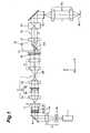
- FIG. 1is an illustration schematically showing a configuration of an exposure apparatus according to an embodiment of the present invention.
- FIG. 2is an illustration to illustrate the action of a conical axicon system on a secondary light source of an annular shape.
- FIG. 3is an illustration to illustrate the action of a zoom lens on a secondary light source of an annular shape.
- FIG. 4is a perspective view schematically showing an internal configuration of a polarization monitor in FIG. 1 .
- FIG. 5is an illustration schematically showing a configuration of a polarization-modulating element in FIG. 1 .
- FIG. 6is an illustration to illustrate the optical activity of crystalline quartz.
- FIG. 7is an illustration schematically showing a secondary light source of an annular shape set in a azimuthal polarization state by the action of the polarization-modulating element.
- FIG. 8is an illustration schematically showing a secondary light source of an annular shape set in a radially polarized state by the action of the polarization-modulating element.
- FIG. 9is an illustration showing a modification example in which a plurality of polarization-modulating elements are arranged in a replaceable state.
- FIG. 10is an illustration showing plural types of polarization-modulating elements 10 a - 10 c mounted on a turret 10 T as a replacing mechanism in FIG. 9 .
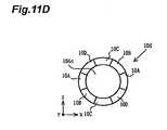
- FIGS. 11A , 11 B, 11 C, 11 D and 11 Eare illustrations showing respective configurations of plural types of polarization-modulating elements 10 a - 10 e, respectively.
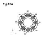
- FIGS. 12A , 12 B and 12 Care illustrations schematically showing examples of the secondary light source set in the azimuthal polarization state by the action of the polarization-modulating element, respectively.
- FIG. 13is an illustration schematically showing a configuration of polarization-modulating element 10 f arranged rotatable around the optical axis AX.
- FIGS. 14A , 14 B and 14 Care illustrations schematically showing examples of the secondary light source set in the azimuthal polarization state by the action of polarization-modulating element 10 f, respectively.
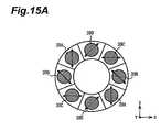
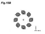
- FIGS. 15A , 15 B and 15 Care illustrations schematically showing examples of the secondary light source obtained when the polarization-modulating element composed of elementary elements of a sector shape is arranged rotatable around the optical axis AX, respectively.
- FIG. 16is an illustration showing an example in which the polarization-modulating element is located at a position immediately before conical axicon system 8 (or at a position near the entrance side), among locations near the pupil of the illumination optical apparatus.
- FIG. 17is an illustration for explaining Conditions (1) and (2) to be satisfied in the modification example shown in FIG. 16 .
- FIG. 18is an illustration showing an example in which the polarization-modulating element is located near the pupil position of imaging optical system 15 , among locations near the pupil of the illumination optical apparatus.
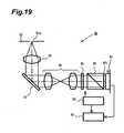
- FIG. 19is an illustration showing a schematic configuration of wafer surface polarization monitor 90 for detecting a polarization state and light intensity of light illuminating a wafer W.
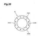
- FIG. 20is an illustration showing a secondary light source 31 of an annular shape obtained when a quartered polarization-modulating element 10 f is used to implement quartered, circumferentially polarized annular illumination.
- FIG. 21is a flowchart of a procedure of producing semiconductor devices as microdevices.
- FIG. 22is a flowchart of a procedure of producing a liquid crystal display element as a microdevice.
- FIG. 1is an illustration schematically showing a configuration of an exposure apparatus according to an embodiment of the present invention.
- the Z-axisis defined along a direction of a normal to a wafer W being a photosensitive substrate, the Y-axis along a direction parallel to the plane of FIG. 1 in the plane of the wafer W, and the X-axis along a direction of a normal to the plane of FIG. 1 in the plane of wafer W.
- the exposure apparatus of the present embodimentis provided with a light source 1 for supplying exposure radiation (light) [(illumination light)].
- the light source 1can be, for example, a KrF excimer laser light source for supplying light with the wavelength of 248 nm, an ArF excimer laser light source for supplying light with the wavelength of 193 nm, or the like.
- a nearly parallel beam emitted along the Z-direction from the light source 1has a cross section of a rectangular shape elongated along the X-direction, and is incident to a beam expander 2 consisting of a pair of lenses 2 a and 2 b.
- the lenses 2 a and 2 bhave a negative refracting power and a positive refracting power, respectively, in the plane of FIG. 1 (or in the YZ plane). Therefore, the beam incident to the beam expander 2 is enlarged in the plane of FIG. 1 and shaped into a beam having a cross section of a predetermined rectangular shape.
- the nearly parallel beam passing through the beam expander 2 as a beam shaping optical systemis deflected into the Y-direction by a bending mirror 3 , and then travels through a quarter wave plate 4 a, a half wave plate 4 b, a depolarizer (depolarizing element) 4 c, and a diffractive optical element 5 for annular illumination to enter an afocal lens 6 .
- the quarter wave plate 4 a, half wave plate 4 b, and depolarizer 4 cconstitute a polarization state converter 4 , as described later.
- the afocal lens 6is an afocal system (afocal optic) set so that the front focal position thereof approximately coincides with the position of the diffractive optical element 5 and so that the rear focal position thereof approximately coincides with the position of a predetermined plane 7 indicated by a dashed line in the drawing.
- a diffractive optical elementis constructed by forming level differences with the pitch of approximately the wavelength of exposure light (illumination light) in a substrate and has the action of diffracting an incident beam at desired angles.
- the diffractive optical element 5 for annular illuminationhas the following function: when a parallel beam having a rectangular cross section is incident thereto, it forms a light intensity distribution of an annular shape in its far field (or Fraunhofer diffraction region).
- the nearly parallel beam incident to the diffractive optical element 5 as a beam transforming elementforms a light intensity distribution of an annular shape on the pupil plane of the afocal lens 6 and then emerges as a nearly parallel beam from the afocal lens 6 .
- a conical axicon system 8arranged on or near the pupil plane thereof, and the detailed configuration and action thereof will be described later.
- the fundamental configuration and actionwill be described below, in disregard of the action of the conical axicon system 8 .
- the beam through the afocal lens 6travels through a zoom lens 9 for variation of ⁇ -value and a polarization-modulating element 10 and then enters a micro fly's eye lens (or fly's eye lens) 11 as an optical integrator.
- the configuration and action of the polarization-modulating element 10will be described later.
- the micro fly's eye lens 11is an optical element consisting of a number of micro lenses with a positive refracting power arranged lengthwise and breadthwise and densely.
- a micro fly's eye lensis constructed, for example, by forming a micro lens group by etching of a plane-parallel plate.
- each micro lens forming the micro fly's eye lensis much smaller than each lens element forming a fly's eye lens.
- the micro fly's eye lensis different from the fly's eye lens consisting of lens elements spaced from each other, in that a number of micro lenses (micro refracting surfaces) are integrally formed without being separated from each other.
- the micro fly's eye lensis a wavefront splitting optical integrator of the same type as the fly's eye lens.
- the position of the predetermined plane 7is arranged near the front focal position of the zoom lens 9 , and the entrance surface of the micro fly's eye lens 11 is arranged near the rear focal position of the zoom lens 9 .
- the zoom lens 9arranges the predetermined plane 7 and the entrance surface of the micro fly's eye lens 11 substantially in the relation of Fourier transform and eventually arranges the pupil plane of the afocal lens 6 and the entrance surface of the micro fly's eye lens 11 approximately optically conjugate with each other.
- an illumination field of an annular shape centered around the optical axis AXis formed on the entrance surface of the micro fly's eye lens 11 , as on the pupil plane of the afocal lens 6 .
- the entire shape of this annular illumination fieldsimilarly varies depending upon the focal length of the zoom lens 9 .
- Each micro lens forming the micro fly's eye lens 11has a rectangular cross section similar to a shape of an illumination field to be formed on a mask M (eventually, a shape of an exposure region to be formed on a wafer W).
- the beam incident to the micro fly's eye lens 11is two-dimensionally split by a number of micro lenses to form on or near the rear focal plane (eventually on the illumination pupil) a secondary light source having much the same light intensity distribution as the illumination field formed by the incident beam, i.e., a secondary light source consisting of a substantial surface illuminant of an annular shape centered around the optical axis AX.
- Beams from the secondary light source formed on or near the rear focal plane of the micro fly's eye lens 11travel through beam splitter 12 a and condenser optical system 13 to superposedly illuminate a mask blind 14 .
- an illumination field of a rectangular shape according to the shape and focal length of each micro lens forming the micro fly's eye lens 11is formed on the mask blind 14 as an illumination field stop.
- the internal configuration and action of polarization monitor 12 incorporating a beam splitter 12 awill be described later. Beams through a rectangular aperture (light transmitting portion) of the mask blind 14 are subject to light condensing action of imaging optical system 15 and thereafter superposedly illuminate the mask M on which a predetermined pattern is formed.
- the imaging optical system 15forms an image of the rectangular aperture of the mask blind 14 on the mask M.
- a beam passing through the pattern of mask Mtravels through a projection optical system PL to form an image of the mask pattern on the wafer W being a photosensitive substrate.
- the pattern of the mask Mis sequentially printed in each exposure area on the wafer W through full-wafer exposure or scan exposure with two-dimensional drive control of the wafer W in the plane (XY plane) perpendicular to the optical axis AX of the projection optical system PL.
- the quarter wave plate 4 ais arranged so that its crystallographic axis is rotatable around the optical axis AX, and it transforms incident light of elliptical polarization into light of linear polarization.
- the half wave plate 4 bis arranged so that its crystallographic axis is rotatable around the optical axis AX, and it changes the plane of polarization of linearly polarized light incident thereto.
- the depolarizer 4 cis composed of a wedge-shaped crystalline quartz prism and a wedge-shaped fused silica prism having complementary shapes.
- the crystalline quartz prism and the fused silica prismare constructed as an integral prism assembly so as to be set into and away from the illumination optical path.
- the light source 1is the KrF excimer laser light source or the ArF excimer laser light source
- light emitted from these light sourcestypically has the degree of polarization of 95% or more and light of almost linear polarization is incident to the quarter wave plate 4 a.
- a right-angle prism as a back-surface reflectoris interposed in the optical path between the light source 1 and the polarization state converter 4 , the linearly polarized light will be changed into elliptically polarized light by virtue of total reflection in the right-angle prism unless the plane of polarization of the incident, linearly polarized light agrees with the P-polarization plane or S-polarization plane.
- the polarization state converter 4for example, even if light of elliptical polarization is incident thereto because of the total reflection in the right-angle prism, light of linear polarization transformed by the action of the quarter wave plate 4 a will be incident to the half wave plate 4 b. Where the crystallographic axis of the half wave plate 4 b is set at an angle of 0° or 90° relative to the plane of polarization of the incident, linearly polarized light, the light of linear polarization incident to the half wave plate 4 b will pass as it is, without change in the plane of polarization.
- the crystallographic axis of the half wave plate 4 bis set at an angle of 45° relative to the plane of polarization of the incident, linearly polarized light
- the light of linear polarization incident to the half wave plate 4 bwill be transformed into light of linear polarization with change of polarization plane of 90°.
- the crystallographic axis of the crystalline quartz prism in the depolarizer 4 cis set at an angle of 45° relative to the polarization plane of the incident, linearly polarized light
- the light of linear polarization incident to the crystalline quartz prismwill be transformed (or depolarized) into light in an unpolarized state.
- the polarization state converter 4is arranged as follows: when the depolarizer 4 c is positioned in the illumination optical path, the crystallographic axis of the crystalline quartz prism makes the angle of 45° relative to the polarization plane of the incident, linearly polarized light. Incidentally, where the crystallographic axis of the crystalline quartz prism is set at the angle of 0° or 90° relative to the polarization plane of the incident, linearly polarized light, the light of linear polarization incident to the crystalline quartz prism will pass as it is, without change of the polarization plane.
- the crystallographic axis of the half wave plate 4 bis set at an angle of 22.5° relative to the polarization plane of incident, linearly polarized light
- the light of linear polarization incident to the half wave plate 4 bwill be transformed into light in an unpolarized state including a linear polarization component directly passing without change of the polarization plane and a linear polarization component with the polarization plane rotated by 90°.
- the polarization state converter 4is arranged so that light of linear polarization is incident to the half wave plate 4 b, as described above, and, for easier description hereinafter, it is assumed that light of linear polarization having the direction of polarization (direction of the electric field) along the Z-axis in FIG. 1 (hereinafter referred to as “Z-directionally polarized light”) is incident to the half wave plate 4 b.
- the depolarizer 4 cWhen the depolarizer 4 c is positioned in the illumination optical path and when the crystallographic axis of the half wave plate 4 b is set at the angle of 0° or 90° relative to the polarization plane (direction of polarization) of the Z-directionally polarized light incident thereto, the light of Z-directional polarization incident to the half wave plate 4 b passes as kept as Z-directionally polarized light without change of the polarization plane and enters the crystalline quartz prism in the depolarizer 4 c.
- the crystallographic axis of the crystalline quartz prismis set at the angle of 45° relative to the polarization plane of the Z-directionally polarized light incident thereto, the light of Z-directional polarization incident to the crystalline quartz prism is transformed into light in an unpolarized state.
- the light depolarized through the crystalline quartz prismtravels through the quartz prism as a compensator for compensating the traveling direction of the light and is incident into the diffractive optical element 5 while being in the depolarized state.
- the crystallographic axis of the half wave plate 4 bis set at the angle of 45° relative to the polarization plane of the Z-directionally polarized light incident thereto, the light of Z-directional polarization incident to the half wave plate 4 b will be rotated in the polarization plane by 90° and transformed into light of linear polarization having the polarization direction (direction of the electric field) along the X-direction in FIG.
- X-directionally polarized light(hereinafter referred to as “X-directionally polarized light”) and the X-directionally polarized light will be incident to the crystalline quartz prism in the depolarizer 4 c. Since the crystallographic axis of the crystalline quartz prism is set at the angle of 45° relative to the polarization plane of the incident, X-directionally polarized light as well, the light of X-directional polarization incident to the crystalline quartz prism is transformed into light in the depolarized state, and the light travels through the quartz prism to be incident in the depolarized state into the diffractive optical element 5 .
- the depolarizer 4 cwhen the depolarizer 4 c is set away from the illumination optical path, if the crystallographic axis of the half wave plate 4 b is set at the angle of 0° or 90° relative to the polarization plane of the Z-directionally polarized light incident thereto, the light of Z-directional polarization incident to the half wave plate 4 b will pass as kept as Z-directionally polarized light without change of the polarization plane, and will be incident in the Z-directionally polarized state into the diffractive optical element 5 .
- the crystallographic axis of the half wave plate 4 bis set at the angle of 45° relative to the polarization plane of the Z-directionally polarized light incident thereto on the other hand, the light of Z-directional polarization incident to the half wave plate 4 b will be transformed into light of X-directional polarization with the polarization plane rotated by 90°, and will be incident in the X-directionally polarized state into the diffractive optical element 5 .
- the light in the depolarized statecan be made incident to the diffractive optical element 5 when the depolarizer 4 c is set and positioned in the illumination optical path.
- the depolarizer 4 cis set away from the illumination optical path and when the crystallographic axis of the half wave plate 4 b is set at the angle of 0° or 90° relative to the polarization plane of the Z-directionally polarized light incident thereto, the light in the Z-directionally polarized state can be made incident to the diffractive optical element 5 .
- the depolarizer 4 cwhen the depolarizer 4 c is set away from the illumination optical path and when the crystallographic axis of the half wave plate 4 b is set at the angle of 45° relative to the polarization plane of the Z-directionally polarized light incident thereto, the light in the X-directionally polarized state can be made incident to the diffractive optical element 5 .
- the polarization state converter 4is able to switch the polarization state of the incident light into the diffractive optical element 5 (therefore, the polarization state of light to illuminate the mask M and wafer W) between the linearly polarized state and the unpolarized state through the action of the polarization state converter consisting of the quarter wave plate 4 a, half wave plate 4 b, and depolarizer 4 c, and, in the case of the linearly polarized state, it is able to switch between mutually orthogonal polarization states (between the Z-directional polarization and the X-directional polarization).
- the polarization state converter 4when the polarization state converter 4 is so set that the half wave plate 4 b and depolarizer 4 c both are set away from the illumination optical path and that the crystallographic axis of the quarter wave plate 4 a makes a predetermined angle relative to the incident, elliptically polarized light, light in a circularly polarized state can be made incident to the diffractive optical element 5 .
- the polarization state of incident light to the diffractive optical element 5can also be set in a linearly polarized state having a direction of polarization along an arbitrary direction by the action of the half wave plate 4 b.
- the conical axicon system 8is composed of a first prism member 8 a whose plane is kept toward the light source and whose refracting surface of a concave conical shape is kept toward the mask, and a second prism member 8 b whose plane is kept toward the mask and whose refracting surface of a convex conical shape is kept toward the light source, in order from the light source side.
- the refracting surface of the concave conical shape of the first prism member 8 a and the refracting surface of the convex conical shape of the second prism member 8 bare formed in a complementary manner so as to be able to be brought into contact with each other.
- At least one of the first prism member 8 a and the second prism member 8 bis arranged movable along the optical axis AX, so that the spacing can be varied between the refracting surface of the concave conical shape of the first prism member 8 a and the refracting surface of the convex conical shape of the second prism member 8 b.
- the conical axicon system 8functions as a plane-parallel plate and has no effect on the secondary light source of the annular shape formed.
- the conical axicon system 8functions a so-called beam expander. Therefore, the angle of the incident beam to the predetermined plane 7 varies according to change in the spacing of the conical axicon system 8 .
- FIG. 2is an illustration to illustrate the action of the conical axicon system on the secondary light source of the annular shape.
- the secondary light source 30 a of the minimum annular shape formed in a state where the spacing of the conical axicon system 8 is zero and where the focal length of the zoom lens 9 is set at the minimum(this state will be referred to hereinafter as a “standard state”) is changed into secondary light source 30 b of an annular shape with the outside diameter and inside diameter both enlarged and without change in the width (half of the difference between the inside diameter and the outside diameter: indicated by arrows in the drawing) when the spacing of the conical axicon system 8 is increased from zero to a predetermined value.
- an annular ratio (inside diameter/outside diameter) and size (outside diameter)both vary through the action of the conical axicon system 8 , without change in the width of the secondary light source of the annular shape.
- FIG. 3is an illustration to illustrate the action of the zoom lens on the secondary light source of the annular shape.
- the secondary light source 30 a of the annular shape formed in the standard stateis changed into secondary light source 30 c of an annular shape whose entire shape is similarly enlarged by increasing the focal length of the zoom lens 9 from the minimum to a predetermined value.
- the width and size (outside diameter)both vary through the action of zoom lens 9 , without change in the annular ratio of the secondary light source of the annular shape.
- FIG. 4is a perspective view schematically showing the internal configuration of the polarization monitor shown in FIG. 1 .
- the polarization monitor 12is provided with a first beam splitter 12 a disposed in the optical path between the micro fly's eye lens 11 and the condenser optical system 13 .
- the first beam splitter 12 ahas, for example, the form of a non-coated plane-parallel plate made of quartz glass (i.e., raw glass), and has a function of taking reflected light in a polarization state different from a polarization state of incident light, out of the optical path.
- the light taken out of the optical path by the first beam splitter 12 ais incident to a second beam splitter 12 b.
- the second beam splitter 12 bhas, for example, the form of a non-coated plane-parallel plate made of quartz glass as the first beam splitter 12 a does, and has a function of generating reflected light in a polarization state different from the polarization state of incident light.
- the polarization monitoris so set that the P-polarized light for the first beam splitter 12 a becomes the S-polarized light for the second beam splitter 12 b and that the S-polarized light for the first beam splitter 12 a becomes the P-polarized light for the second beam splitter 12 b.
- first light intensity detector 12 cLight transmitted by the second beam splitter 12 b is detected by first light intensity detector 12 c, while light reflected by the second beam splitter 12 b is detected by second light intensity detector 12 d.
- Outputs from the first light intensity detector 12 c and from the second light intensity detector 12 dare supplied each to a controller (not shown).
- the controllerdrives the quarter wave plate 4 a, half wave plate 4 b, and depolarizer 4 c constituting the polarization state converter 4 , according to need.
- the reflectance for the P-polarized light and the reflectance for the S-polarized lightare substantially different in the first beam splitter 12 a and in the second beam splitter 12 b.
- the reflected light from the first beam splitter 12 aincludes the S-polarization component (i.e., the S-polarization component for the first beam splitter 12 a and P-polarization component for the second beam splitter 12 b ), for example, which is approximately 10% of the incident light to the first beam splitter 12 a, and the P-polarization component (i.e., the P-polarization component for the first beam splitter 12 a and S-polarization component for the second beam splitter 12 b ), for example, which is approximately 1% of the incident light to the first beam splitter 12 a.
- the S-polarization componenti.e., the S-polarization component for the first beam splitter 12 a and P-polarization component for the second beam splitter 12 b
- the P-polarization componenti.e., the P-polar
- the P-polarization componenti.e., the P-polarization component for the first beam splitter 12 a and S-polarization component for the second beam splitter 12 b
- the S-polarization componenti.e., the S-polarization component for the first beam splitter 12 a and P-polarization component for the second beam splitter 12 b
- the first beam splitter 12 ahas the function of extracting the reflected light in the polarization state different from the polarization state of the incident light out of the optical path in accordance with its reflection characteristic.
- the polarization statedegree of polarization
- the polarization state of the illumination lightto the mask M, based on the output from the first light intensity detector 12 c (information about the intensity of transmitted light from the second beam splitter 12 b, i.e., information about the intensity of light virtually in the same polarization state as that of the reflected light from the first beam splitter 12 a ).
- the polarization monitor 12is so set that the P-polarized light for the first beam splitter 12 a becomes the S-polarized light for the second beam splitter 12 b and that the S-polarized light for the first beam splitter 12 a becomes the P-polarized light for the second beam splitter 12 b.
- the controllerdetermines that the illumination light to the mask M (eventually, to the wafer W) is not in the desired unpolarized state, linearly polarized state, or circularly polarized state, based on the detection result of the polarization monitor 12 , it drives and adjusts the quarter wave plate 4 a, half wave plate 4 b, and depolarizer 4 c constituting the polarization state converter 4 so that the state of the illumination light to the mask M can be adjusted into the desired unpolarized state, linearly polarized state, or circularly polarized state.
- Quadrupole illuminationcan be implemented by setting a diffractive optical element for quadrupole illumination (not shown) in the illumination optical path, instead of the diffractive optical element 5 for annular illumination.
- the diffractive optical element for quadrupole illuminationhas such a function that when a parallel beam having a rectangular cross section is incident thereto, it forms a light intensity distribution of a quadrupole shape in the far field thereof. Therefore, the beam passing through the diffractive optical element for quadrupole illumination forms an illumination field of a quadrupole shape consisting of four circular illumination fields centered around the optical axis AX, for example, on the entrance surface of the micro fly's eye lens 11 .
- the secondary light source of the same quadrupole shape as the illumination field formed on the entrance surfaceis also formed on or near the rear focal plane of the micro fly's eye lens 11 .
- ordinary circular illuminationcan be implemented by setting a diffractive optical element for circular illumination (not shown) in the illumination optical path, instead of the diffractive optical element 5 for annular illumination.
- the diffractive optical element for circular illuminationhas such a function that when a parallel beam having a rectangular cross section is incident thereto, it forms a light intensity distribution of a circular shape in the far field. Therefore, a beam passing through the diffractive optical element for circular illumination forms a circular illumination field centered around the optical axis AX, for example, on the entrance surface of the micro fly's eye lens 11 .
- the secondary light source of the same circular shape as the illumination field formed on the entrance surfaceis also formed on or near the rear focal plane of the micro fly's eye lens 11 .
- multipole illuminationsdipole illumination, octapole illumination, etc.
- diffractive optical elementsfor multipole illuminations (not shown), instead of the diffractive optical element 5 for annular illumination.
- modified illuminations in various formscan be implemented by setting diffractive optical elements with appropriate characteristics (not shown) in the illumination optical path, instead of the diffractive optical element 5 for annular illumination.
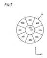
- FIG. 5is an illustration schematically showing the configuration of the polarization-modulating element shown in FIG. 1 .
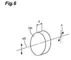
- FIG. 6is an illustration to illustrate the optical activity of crystalline quartz.
- FIG. 7is an illustration schematically showing the secondary light source of the annular shape set in the azimuthal polarization state by the action of the polarization-modulating element.
- the polarization-modulating element 10according to the present embodiment is located immediately before the micro fly's eye lens 11 , i.e., on or near the pupil of the illumination optical apparatus ( 1 to PL). Therefore, in the case of the annular illumination, the beam having an approximately annular cross section centered around the optical axis AX is incident to the polarization-modulating element 10 .
- the polarization-modulating element 10has an effective region of an annular shape centered around the optical axis AX as a whole, and this effective region of the annular shape is composed of eight elementary elements of a sector shape as circumferentially equally divided around the optical axis AX.
- the eight elementary elementsinclude four types of elementary elements 10 A- 10 D two each with different thicknesses (lengths in the direction of the optical axis) along the direction of transmission of light (Y-direction).
- the thickness of the first elementary elements 10 Ais the largest
- the thickness of the fourth elementary elements 10 Dis the smallest
- the thickness of the second elementary elements 10 Bis set larger than the thickness of the third elementary elements 10 C.
- one surface (e.g., the entrance surface) of the polarization-modulating element 10is planar, while the other surface (e.g., the exit surface) is uneven because of the differences among the thicknesses of the elementary elements 10 A- 10 D. It is also possible to form the both surfaces (the entrance surface and exit surface) of the polarization-modulating element 10 in an uneven shape.
- each elementary element 10 A- 10 Dis made of crystalline quartz as a crystalline material being an optical material with optical activity, and the crystallographic axis of each elementary element 10 A- 10 D is set to be approximately coincident with the optical axis AX, i.e., with the traveling direction of incident light.
- the optical activity of crystalline quartzwill be briefly described below with reference to FIG. 6 .
- an optical member 100 of a plane-parallel plate shape made of crystalline quartz and in a thickness dis arranged so that its crystallographic axis coincides with the optical axis AX.
- linearly polarized light incident theretoemerges in a state in which its-polarization direction is rotated by ⁇ around the optical axis AX.
- the rotation angle (angle of optical rotation) ⁇ of the polarization direction due to the optical activity of the optical member 100is represented by Eq (a) below, using the thickness d of the optical member 100 and the rotatory power ⁇ of crystalline quartz.
- the rotatory power ⁇ of crystalline quartzhas wavelength dependence (a property that the value of the optical rotatory power differs depending upon the wavelength of light used: optical rotatory dispersion) and, specifically, it tends to increase with decrease in the wavelength of light used.
- the rotatory power ⁇ of crystalline quartz for light having the wavelength of 250.3 nmis 153.9°/mm.
- the first elementary elements 10 Aare designed in such a thickness dA that when linearly polarized light having the polarization direction along the Z-direction is incident thereto, they output light of linear polarization having the polarization direction along a direction resulting from +180° rotation of the Z-direction around the Y-axis, i.e., along the Z-direction.
- the polarization direction of beams passing through a pair of arc (bow shape) regions 31 A formed by beams subject to the optical rotating action of a pair of first elementary elements 10 A, in the secondary light source 31 of the annular shape shown in FIG. 7is the Z-direction.
- the second elementary elements 10 Bare designed in such a thickness dB that when linearly polarized light having the polarization direction along the Z-direction is incident thereto, they output light of linear polarization having the polarization direction along a direction resulting from +135° rotation of the Z-direction around the Y-axis, i.e., along a direction resulting from ⁇ 45° rotation of the Z-direction around the Y-axis.
- the polarization direction of beams passing through a pair of arc (bow shape) regions 31 B formed by beams subject to the optical rotating action of a pair of second elementary elements 10 B, in the secondary light source 31 of the annular shape shown in FIG. 7is a direction obtained by rotating the Z-direction by ⁇ 45° around the Y-axis.
- the third elementary elements 10 Care designed in such a thickness dC that when linearly polarized light having the polarization direction along the Z-direction is incident thereto, they output light of linear polarization having the polarization direction along a direction resulting from +90° rotation of the Z-direction around the Y-axis, i.e., along the X-direction.
- the polarization direction of beams passing through a pair of arc (bow shape) regions 31 C formed by beams subject to the optical rotating action of a pair of third elementary elements 10 C, in the secondary light source 31 of the annular shape shown in FIG. 7is the X-direction.
- the fourth elementary elements 10 Dare designed in such a thickness dD that when linearly polarized light having the polarization direction along the Z-direction is incident thereto, they output light of linear polarization having the polarization direction along a direction resulting from +45° rotation of the Z-direction around the Y-axis.
- the polarization direction of beams passing through a pair of arc (bow shape) regions 31 D formed by beams subject to the optical rotating action of a pair of fourth elementary elements 10 D, in the secondary light source 31 of the annular shape shown in FIG. 7is a direction obtained by rotating the Z-direction by +45° around the Y-axis.
- the polarization-modulating element 10can be constructed by combining the eight elementary elements prepared separately, or the polarization-modulating element 10 can also be constructed by forming the required uneven shape (level differences) in a crystalline quartz substrate of a plane-parallel plate shape.
- the polarization-modulating element 10is provided with a central region 10 E of a circular shape in the size not less than 3/10, preferably, not less than 1 ⁇ 3 of the radial size of the effective region of the polarization-modulating element 10 and without optical activity.
- the central region 10 Emay be made of an optical material without optical activity, for example, like quartz, or may be simply a circular aperture. It is, however, noted that the central region 10 E is not an essential element for the polarization-modulating element 10 .
- the size of the central region 10 Edetermines the boundary between the region in the azimuthal polarization state and the other region.
- the linearly polarized light having the polarization direction along the Z-directionis made incident to the polarization-modulating element 10 .
- the secondary light source of the annular shape (illumination pupil distribution of annular shape) 31is formed on or near the rear focal plane of the micro fly's eye lens 11 , and beams passing through this secondary light source 31 of the annular shape are set in the azimuthal polarization state.
- the beams passing through the respective arc (bow shape) regions 31 A- 31 D constituting the secondary light source 31 of the annular shapeturn into a linearly polarized state having the polarization direction approximately coincident with a tangential direction to a circle centered around the optical axis AX, at the central position along the circumferential direction of each arc region 31 A- 31 D.
- the present embodimentdifferent from the conventional technology giving rise to the large loss of light quantity at the aperture stop, is able to form the secondary light source 31 of the annular shape in the azimuthal polarization state, with no substantial loss of light quantity, through the optical rotating action of the polarization-modulating element 10 .
- the illumination optical apparatus of the present embodimentis able to form the illumination pupil distribution of the annular shape in the azimuthal polarization state while well suppressing the loss of light quantity.
- the present embodimentuses the polarizing action of the optical elements, it has the excellent effect that the polarization-modulating element itself is extremely easy to produce and, typically, the thickness tolerance of each elementary element can be set to be extremely loose.
- the light illuminating the wafer W as a last surface to be illuminatedis in a polarized state in which the principal component is S-polarized light.
- the S-polarized lightis linearly polarized light having the polarization direction along a direction normal to the plane of incidence (i.e., polarized light with the electric vector oscillating in the direction normal to the plane of incidence).
- the plane of incidenceis defined as follows: when light arrives at a boundary surface of a medium (surface to be illuminated: surface of wafer W), the plane of incidence is a plane including a normal to the boundary surface at that point and the direction of incidence of light.
- the circumferentially polarized annular illuminationrealizes an improvement in the optical performance (depth of focus and the like) of the projection optical system and enables formation of a mask pattern image with high contrast on the wafer (photosensitive substrate).
- the exposure apparatus of the present embodimentuses the illumination optical apparatus capable of forming the illumination pupil distribution of the annular shape in the azimuthal polarization state while well suppressing the loss of light quantity, it is able to transcribe a fine pattern under an appropriate illumination condition faithfully and with high throughput.
- the present embodimentenables radially polarized annular illumination (modified illumination in which beams passing through the secondary light source of the annular shape are set in a radially polarized state) by injecting linearly polarized light having the polarization direction along the X-direction into the polarization-modulating element 10 and thereby setting the beams passing through the secondary light source 32 of the annular shape in the radially polarized state as shown in FIG. 8 .
- beams passing through the respective arc (bow shape) regions 32 A- 32 D constituting the secondary light source 32 of the annular shapeare in the linearly polarized state having the polarization direction approximately coincident with a radial direction of a circle centered around the optical axis AX, at the central position along the circumferential direction of each arc region 32 A- 32 D.
- the light illuminating the wafer W as a last surface to be illuminatedis in a polarized state in which the principal component is P-polarized light.
- the P-polarized lightherein is linearly polarized light having the polarization direction along a direction parallel to the plane of incidence defined as described above (i.e., polarized light with the electric vector oscillating in the direction parallel to the plane of incidence).
- the radially polarized annular illuminationenables formation of a good mask pattern image on the wafer (photosensitive substrate) while keeping the reflectance of light low on the resist applied onto the wafer W.
- the above-described embodimentrealizes the circumferentially polarized annular illumination and the radially polarized annular illumination by switching the beam incident to the polarization-modulating element 10 between the linearly polarized state having the polarization direction along the Z-direction and the linearly polarized state having the polarization direction along the X-direction.
- it is also possible to realize the circumferentially polarized annular illumination and the radially polarized annular illuminationfor example, by switching the polarization-modulating element 10 between a first state shown in FIG. 5 and a second state resulting from 90° rotation around the optical axis AX, for the incident beam in the linearly polarized state having the polarization direction along the Z-direction or along the X-direction.
- the polarization-modulating element 10is located immediately before the micro fly's eye lens 11 .
- the polarization-modulating element 10can also be located generally on or near the pupil of the illumination optical apparatus ( 1 to PL), e.g., on or near the pupil of the projection optical system PL, on or near the pupil of the imaging optical system 15 , or immediately before the conical axicon system 8 (on or near the pupil of afocal lens 6 ).
- the required effective diameter (clear aperture diameter) of the polarization-modulating element 10is prone to become large, and it is rather undesirable in view of the current circumstances in which it is difficult to obtain a large crystalline quartz substrate with high quality.
- the required effective diameter (clear aperture diameter) of the polarization-modulating element 10can be kept small.
- the distanceis long to the wafer W being the last surface to be illuminated, and an element to change the polarization state like an antireflection coat on a lens or a reflecting film on a mirror is likely to be interposed in the optical path to the wafer. Therefore, this arrangement is not so preferable.
- the antireflection coat on the lens or the reflecting film on the mirroris likely to cause the difference of reflectance depending upon the polarization states (P-polarization and S-polarization) and angles of incidence and, in turn, to change the polarization state of light.
- At least one surface of the polarization-modulating element 10is formed in the uneven shape and, therefore, the polarization-modulating element 10 has a thickness profile discretely (discontinuously) varying in the circumferential direction.
- at least one surface of the polarization-modulating element 10can also be formed in such a curved shape that the polarization-modulating element 10 has a thickness profile virtually discontinuously varying in the circumferential direction.
- the polarization-modulating element 10is composed of the eight elementary elements of the sector shape corresponding to the division of the effective region of the annular shape into eight segments.
- the polarization-modulating element 10can also be composed, for example, of eight elementary elements of a sector shape corresponding to division of the effective region of a circular shape into eight segments, or of four elementary elements of a sector shape corresponding to division of the effective region of a circular shape or annular shape into four segments, or of sixteen elementary elements of a sector shape corresponding to division of the effective region of a circular shape or annular shape into sixteen segments.
- a variety of modification examplescan be contemplated as to the shape of the effective region of the polarization-modulating element 10 , the number of segments in the division of the effective region (the number of elementary elements), and so on.
- each elementary element 10 A- 10 D(therefore, the polarization-modulating element 10 ) is made of crystalline quartz.
- each elementary elementcan also be made of another appropriate optical material with optical activity.
- the polarization-modulating element 10is fixedly provided in the illumination optical path, but the polarization-modulating element 10 may be arranged to be set into and away from the illumination optical path.
- the above embodimentshowed the example as a combination of the annular illumination with the S-polarized light for the wafer W, but it is also possible to combine the S-polarized light for the wafer W with multipole illumination, such as dipole or quadrupole illumination, and with circular illumination.
- the illumination conditions for the mask M and the imaging conditions (numerical aperture, aberrations, etc.) for the wafer Wcan be automatically set, for example, according to the type of the pattern on the mask M or the like.
- FIG. 9shows a modification example in which a plurality of polarization-modulating elements are arranged in a replaceable state.
- the modification example of FIG. 9has a configuration similar to the embodiment shown in FIG. 1 , but it is different in that it has a turret 10 T enabling replacement of the plurality of polarization-modulating elements.
- FIG. 10is an illustration showing plural types of polarization-modulating elements 10 a - 10 e mounted on the turret 10 T as a replacing mechanism in FIG. 9 .
- the plural types of polarization-modulating elements 10 a - 10 eare provided on the turret 10 T rotatable around an axis along a direction parallel to the optical axis AX, and these plural types of polarization-modulating elements 10 a - 10 e are arranged replaceable by rotation operation of the turret 10 T.
- FIG. 10is an illustration showing plural types of polarization-modulating elements 10 a - 10 e mounted on the turret 10 T as a replacing mechanism in FIG. 9 .
- the plural types of polarization-modulating elements 10 a - 10 eare provided on the turret 10 T rotatable around an axis along a direction parallel to the optical axis AX, and these plural types of polarization-modulating elements 10 a -
- FIG. 9depicts only the polarization-modulating elements 10 a, 10 b out of the plural types of polarization-modulating elements 10 a - 10 e.
- the replacing mechanism for the polarization-modulating elementsis not limited to the turret 10 T, but may be, for example, a slider.
- FIGS. 11A-11Eare illustrations showing respective configurations of the plural types of polarization-modulating elements 10 a - 10 e.
- the first polarization-modulating element 10 ahas the same configuration as the polarization-modulating element 10 of the embodiment shown in FIG. 5 .
- the second polarization-modulating element 10 bhas a configuration similar to the polarization-modulating element 10 a shown in FIG. 11A , but is different in that it is provided with a depolarizing member 104 c in central region 10 E.
- This depolarizing member 104 chas a configuration similar to the depolarizer 4 c shown in FIG. 1 , and has a function of transforming incident light of linear polarization into light in a depolarized state.
- the third polarization-modulating element 10 chas a configuration similar to the polarization-modulating element 10 a shown in FIG. 11A , but is different in that the size of the central region 10 E is larger (i.e., in that the width of the first to fourth elementary elements 10 A- 10 D is smaller).
- the fourth polarization-modulating element 10 dhas a configuration similar to the polarization-modulating element 10 c shown in FIG. 11C , but is different in that a depolarizing member 104 c is provided in the central region 10 E.
- the fifth polarization-modulating element 10 eis constructed by combining six elementary elements 10 C, 10 F, 10 G, different from the eight elementary elements.
- the fifth polarization-modulating element 10 ehas the effective region of an annular shape centered around the optical axis AX as a whole, and this effective region of the annular shape is composed of six elementary elements 10 C, 10 F, 10 G of a sector shape as equally divided in the circumferential direction around the optical axis AX.
- a pair of elementary elements facing each other with the optical axis AX in betweenhave the same characteristic.
- the six elementary elements 10 C, 10 F, 10 Ginclude three types of elementary elements 10 C, 10 F, 10 G with mutually different thicknesses (lengths in the direction of the optical axis) along the direction of transmission of light (the Y-direction) two each.
- the elementary elements 10 Care members having the same function as the third elementary elements 10 C shown in FIG. 7 , and thus the description of the function thereof is omitted herein.
- the elementary elements 10 Fare designed in such a thickness dF that when linearly polarized light having the polarization direction along the Z-direction is incident thereto, they output light of linear polarization having the polarization direction along a direction resulting from +150° rotation of the Z-direction around the Y-axis, i.e., along a direction resulting from ⁇ 30° rotation of the Z-direction around the Y-axis.
- the elementary elements 10 Gare designed in such a thickness dG that when linearly polarized light having the polarization direction along the Z-direction is incident thereto, they output light of linear polarization having the polarization direction along a direction resulting from +30° rotation of the Z-direction around the Y-axis.
- a depolarizing member 104 cmay be provided in place of the central region 10 E.
- FIGS. 12A-12Care illustrations schematically showing examples of the secondary light source set in the azimuthal polarization state by the action of the polarization-modulating element.
- the polarization-modulating elementis also illustrated in a superimposed manner in order to facilitate understanding.
- FIG. 12Ashows the secondary light source 33 of an octapole shape in a case where a diffractive optical element (beam transforming element) for forming a light intensity distribution of an octapole shape in the far field (or Fraunhofer diffraction region) is located in the illumination optical path, instead of the diffractive optical element 5 , and where the polarization-modulating element 10 a or 10 b is located in the illumination optical path. Beams passing through the secondary light source 33 of the octapole shape are set in the azimuthal polarization state.
- a diffractive optical elementbeam transforming element
- the beams passing through the respective eight circular regions 33 A- 33 D constituting the secondary light source 33 of the octapole shapeare in the linearly polarized state having the polarization direction approximately coincident with a circumferential direction of a circle connecting these eight circular regions 33 A- 33 D, i.e., with a tangential direction to the circle connecting these eight circular regions 33 A- 33 D.
- FIG. 12Ashows the example wherein the secondary light source 33 of the octapole shape is composed of the eight circular regions 33 A- 33 D, but the shape of the eight regions is not limited to the circular shape.
- FIG. 12Bshows the secondary light source 34 of a quadrupole shape in a case where a diffractive optical element (beam transforming element) for forming a light intensity distribution of a quadrupole shape in the far field (or Fraunhofer diffraction region) is located in the illumination optical path, instead of the diffractive optical element 5 , and where the polarization-modulating element 10 c or 10 d is located in the illumination optical path. Beams passing through the secondary light source 34 of the quadrupole shape are set in the azimuthal polarization state.
- a diffractive optical elementbeam transforming element
- the beams passing through the respective four regions 34 A, 34 C constituting the secondary light source 34 of the quadrupole shapeare in the linearly polarized state having the polarization direction approximately coincident with a circumferential direction of a circle connecting these four regions 34 A, 34 C, i.e., with a tangential direction to the circle connecting these four regions 34 A, 34 C.
- FIG. 12Bshows the example wherein the secondary light source 34 of the quadrupole shape is composed of four regions 34 A, 34 C of an almost elliptical shape, but the shape of the four regions is not limited to the almost elliptical shape.
- FIG. 12Cshows the secondary light source 35 of a hexapole shape in a case where a diffractive optical element (beam transforming element) for forming a light intensity distribution of a hexapole shape in the far field (or Fraunhofer diffraction region) is located in the illumination optical path, instead of the diffractive optical element 5 , and where the polarization-modulating element 10 e is located in the illumination optical path. Beams passing through the secondary light source 35 of the hexapole shape are set in the azimuthal polarization state.
- a diffractive optical elementbeam transforming element
- the beams passing through the respective six regions 35 C, 35 F, 35 G constituting the secondary light source 35 of the hexapole shapeare in the linearly polarized state having the polarization direction approximately coincident with a circumferential direction of a circle connecting these six regions 35 C, 35 F, 35 G, i.e., with a tangential direction to the circle connecting these six regions 35 C, 35 F, 35 G
- FIG. 12Cshows the example wherein the secondary light source 35 of the hexapole shape is composed of the four regions 35 C, 35 F, 35 G of an almost trapezoidal shape, but the shape of the six regions is not limited to the almost trapezoidal shape.
- FIG. 13is an illustration schematically showing a configuration of polarization-modulating element 10 f arranged rotatable around the optical axis AX.
- the polarization-modulating element 10 fis composed of a combination of four elementary elements 10 A, 10 C.
- the polarization-modulating element 10 fhas the effective region of an annular shape centered around the optical axis AX as a whole, and this effective region of the annular shape is composed of four elementary elements 10 A, 10 C of a sector shape as equally divided in the circumferential direction around the optical axis AX.
- these four elementary elements 10 A, 10 Ca pair of elementary elements facing each other with the optical axis AX in between have the same characteristic.
- the four elementary elements 10 A, 10 Cinclude two types of elementary elements 10 A, 10 C two each with mutually different thicknesses (lengths in the direction of the optical axis) along the direction of transmission of light (the Y-direction).
- the elementary elements 10 Aare members having the same function as the first elementary elements 10 A shown in FIG. 7 , and the elementary elements 10 C members having the same function as the third elementary elements 10 C shown in FIG. 7 . Therefore, the description of the functions is omitted herein.
- a depolarizing member 104 cmay be provided in place of the central region 10 E.
- This-polarization-modulating element 10 fis arranged to be rotatable around the optical axis AX and, for example, is rotatable by +45° or ⁇ 45° around the optical axis AX.
- FIGS. 14A-14Care illustrations schematically showing examples of the secondary light source set in the azimuthal polarization state by the action of the polarization-modulating element 10 f. In FIGS. 14A-14C , the polarization-modulating element 10 f is also illustrated in a superimposed manner in order to facilitate understanding.
- FIG. 14Ashows the secondary light source 36 ( 36 A) of a dipole shape in a case where a diffractive optical element (beam transforming element) for forming a light intensity distribution of a dipole shape in the far field (or Fraunhofer diffraction region) is set in the illumination optical path, instead of the diffractive optical element 5 , and where the polarization-modulating element 10 f is located in a state at the rotation angle of 0° (standard state) in the illumination optical path.
- beams passing through the secondary light source 36 ( 36 A) of the dipole shapeare set in a vertically polarized state.
- FIG. 14Bshows the secondary light source 37 of a quadrupole shape in a case where a diffractive optical element (beam transforming element) for forming a light intensity distribution of a quadrupole shape in the far field (or Fraunhofer diffraction region) is located in the illumination optical path, instead of the diffractive optical element 5 , and where the polarization-modulating element 10 f is located in the state at the rotation angle of 0° (standard state) in the illumination optical path.
- beams passing through the secondary light source 37 of the quadrupole shapeare set in the azimuthal polarization state.
- the light intensity distribution of the quadrupole shape in FIG. 14Bis localized in the vertical direction (Z-direction) and in the horizontal direction (X-direction) in the plane of the drawing.
- FIG. 14Bshows the example in which the secondary light source 37 of the quadrupole shape is composed of the four circular regions 37 A, 37 C, but the shape of the four regions is not limited to the circular shape.
- FIG. 14Cshows the secondary light source 38 of a quadrupole shape in a case where a diffractive optical element (beam transforming element) for forming a light intensity distribution of a quadrupole shape localized in the direction of +45° ( ⁇ 135°) in the plane of the drawing and in the direction of ⁇ 45° (+135°) in the plane of the drawing in the far field (or Fraunhofer diffraction region) is located in the illumination optical path, instead of the diffractive optical element shown in FIG.
- a diffractive optical elementbeam transforming element
- the polarization-modulating element 10 fis set in a rotated state at the rotation angle of +45° (i.e., in a state in which it is rotated by 45° clockwise relative to the standard state) in the illumination optical path.
- the half wave plate 4 b in the polarization state converter 4is rotated around the optical axis, whereby the linearly polarized light having the polarization direction along the direction of +45° (the direction of ⁇ 135°) is made incident to the polarization-modulating element 10 f.
- the elementary elements 10 Ahave the function of rotating the polarization direction of the incident, linearly polarized light by 180° ⁇ n 180° (n is an integer)
- the elementary elements 10 Chave the function of rotating the polarization direction of the incident, linearly polarized light by 90° ⁇ n 180° (n is an integer). Therefore, beams passing through the secondary light source 38 of the quadrupole shape are set in the azimuthal polarization state.
- FIG. 14Cshows the example in which the secondary light source 38 of the quadrupole shape is composed of the four circular regions 38 B, 38 D, but the shape of the four regions is not limited to the circular shape.
- the azimuthal polarization statecan be realized by the secondary light source of the quadrupole shape localized in the +45° ( ⁇ 135°) direction and in the ⁇ 45° (+135°) direction, by the secondary light source of the quadrupole shape localized in the 0° (+180°) direction and in the 90° (270°) direction or in the vertical and horizontal directions, or by the secondary light source of the dipole shape localized in the 0° (+180°) direction or in the 90° (270°) direction, i.e., in the vertical or horizontal direction.
- the polarization-modulating element composed of the eight elementary elements of the sector shape as equally divided in the circumferential direction around the optical axis AXmay be arranged rotatable around the optical axis AX. For example, when the polarization-modulating element composed of the eight divisional elementary elements (e.g., the polarization-modulating element 10 a ) is rotated by +45° around the optical axis AX, as shown in FIG.
- the beams passing through the respective eight circular regions 39 A- 39 D constituting the secondary light source 39 of the octapole shapeare in the linearly polarized state having the polarization direction resulting from ⁇ 45° rotation relative to the circumferential direction of the circle connecting these eight circular regions 39 A- 39 D (i.e., relative to the tangential direction to the circle connecting these eight circular regions 39 A- 39 D).
- an approximately azimuthal polarization statecan be achieved, as shown in FIG. 15C , by rotating the polarization-modulating element (e.g., polarization-modulating element 10 a ) by +45° around the optical axis AX as shown in FIG. 15A .
- the polarization-modulating elemente.g., polarization-modulating element 10 a
- FIG. 16shows an example in which the polarization-modulating element is located at a position immediately before the conical axicon system 8 (i.e., at a position near the entrance side), among locations near the pupil of the illumination optical apparatus.
- the polarization-modulating elementis located at a position immediately before the conical axicon system 8 (i.e., at a position near the entrance side), among locations near the pupil of the illumination optical apparatus.
- the zoom action of the zoom lens system 9results in changing the size of the image of the central region 10 E projected onto the entrance surface of micro fly's eye lens 11 and the size of the images of the respective elementary elements 10 A- 10 D projected onto the entrance surface of micro fly's eye lens 11
- the operation of the conical axicon system 8results in changing the width in the radial direction around the optical axis AX in the images of the respective elementary elements 10 A- 10 D projected onto the entrance surface of micro fly's eye lens 11 .
- the size of the central region 10 Ecan be determined with consideration to the fact that the region occupied by the central region 10 E is changed with zooming of the zoom lens 9 .
- the apparatusis preferably configured to satisfy at least one of Conditions (1) and (2) below, as shown in FIG. 17 .
- ⁇ Aincrease of the inside radius of the beam having passed through the optical system with the action of changing the annular ratio.
- Condition (1)the width of the region of the annular shape transformed into the azimuthal polarization state by the polarization-modulating element 10 will become too small to achieve the circumferentially polarized illumination based on the secondary light source of the annular shape or multipole shape at a small annular ratio; thus it is undesirable.
- Condition (2)the diameter of the beam passing through the central region of the polarization-modulating element 10 will become too small to achieve small- ⁇ illumination without change in the polarization state, for example, unless the polarization-modulating element 10 is set off the illumination optical path; thus it is undesirable.
- the polarization-modulating elementmay be located at a position nearer the mask than the micro fly's eye lens 11 , among locations near the pupil of the illumination optical apparatus; specifically, near the pupil position of the imaging optical system 15 for projecting the image of mask blind 14 onto the mask.
- the plurality of polarization-modulating elementsmay also be arranged replaceable as in the embodiment in FIGS. 9 to 11 .
- the polarization directioncan vary by virtue of this-polarization aberration.
- the direction of the plane of polarization rotated by the polarization-modulating element 10can be set in consideration of the influence of the polarization aberration of these optical systems.
- a reflecting memberis located in the optical path on the wafer W side with respect to the polarization-modulating element 10 , a phase difference can occur between polarization directions of light reflected by this reflecting member.
- the direction of the plane of polarization rotated by the polarization-modulating element 10can be set in consideration of the phase difference of the beam caused by the polarization characteristic of the reflecting surface.
- the polarization state of the beam arriving at the wafer W as a photosensitive substrateis detected using a wafer surface polarization monitor 90 which can be attached to a side of a wafer stage (substrate stage) holding the wafer W as a photosensitive substrate.
- the wafer surface polarization monitor 90may be provided in the wafer stage or in a measurement stage separate from the wafer stage.
- FIG. 19is an illustration showing a schematic configuration of the wafer surface polarization monitor 90 for detecting the polarization state and optical intensity of the light illuminating the wafer W.
- the wafer surface polarization monitor 90is provided with a pinhole member 91 which can be positioned at or near the position of the wafer W Light passing through a pinhole 91 a in the pinhole member 91 travels through a collimating lens 92 located so that its front focal position is at or near the position of the image plane of the projection optical system PL, to become a nearly parallel beam, and the beam is reflected by a reflector 93 to enter a relay lens system 94 .
- the nearly parallel beam passing through the relay lens system 94travels through a quarter wave plate 95 as a phase shifter and through a polarization beam splitter 96 as a polarizer, and then reaches a detection surface 97 a of two-dimensional CCD 97 .
- the detection surface 97 a of two-dimensional CCD 97is approximately optically conjugate with the exit pupil of the projection optical system PL and is thus approximately optically conjugate with the illumination pupil plane of the illumination optical apparatus.
- the quarter wave plate 95is arranged rotatable around the optical axis and a setting member 98 for setting the angle of rotation around the optical axis is connected to this quarter wave plate 95 .
- the wafer surface polarization monitor 90is able to detect the change in the light intensity distribution on the detection surface 97 a with rotation of the quarter wave plate 95 around the optical axis by means of the setting member 98 and thereby to measure the polarization state of the illumination light from the detection result by the rotating compensator method.
- the rotating compensator methodis detailed, for example, in Tsuruta, “Pencil of Light—Applied Optics for optical engineers,” K. K. Shingijutsu Communications.
- the polarization state of the illumination lightis measured at a plurality of positions on the wafer surface while the pinhole member 90 (therefore, pinhole 90 a ) is two-dimensionally moved along the wafer surface.
- the wafer surface polarization monitor 90detects a change of the light intensity distribution on the two-dimensional detection surface 97 a, whereby it can measure a distribution of polarization states of the illumination light in the pupil on the basis of the detected distribution information.
- the wafer surface polarization monitor 90can also be configured using a half wave plate instead of the quarter wave plate 95 as a phase shifter.
- a half wave plateinstead of the quarter wave plate 95 as a phase shifter.
- phase shifterin order to measure the polarization state, i.e., the four Stokes parameters, it is necessary to detect the change of the light intensity distribution on the detection surface 97 a in at least four different states, by changing the relative angle around the optical axis between the phase shifter and the polarizer (polarization beam splitter 96 ) or by moving the phase shifter or the polarizer away from the optical path.
- the present embodimentis configured to rotate the quarter wave plate 95 as a phase shifter around the optical axis, but the polarization beam splitter 96 as a polarizer may be rotated around the optical axis, or both of the phase shifter and the polarizer may be rotated around the optical axis. Instead of this operation, or in addition to this operation, one or both of the quarter wave plate 95 as a phase shifter and the polarization beam splitter 96 as a polarizer may be moved into and away from the optical path.
- the polarization state of lightcan vary depending upon the polarization characteristic of the reflector 93 .
- the polarization characteristic of the reflector 93is preliminarily known, the polarization state of the illumination light can be accurately measured by compensating the measurement result of the wafer surface polarization monitor 90 on the basis of the influence of the polarization characteristic of reflector 93 on the polarization state by some calculation.
- the polarization state of the illumination lightcan also be accurately measured by compensating the measurement result in the same manner.
- a degree of specific polarization DSPis first calculated for each of rays passing a point (or a microscopic area) on the pupil and arriving at a point (microscopic area) on the image plane.
- the XYZ coordinate system used in FIGS. 1 , 16 , and 18will be used in the description hereinafter.
- the above-described point (microscopic area) on the pupilcorresponds to a pixel in the two-dimensional CCD 97 , and the point (microscopic area) on the image plane to XY coordinates of the pinhole 90 a.
- Ixis the intensity of the component of X-directional polarization (polarization with the direction of oscillation along the X-direction on the pupil) in a specific ray passing a point (or microscopic area) on the pupil and arriving at a point (microscopic area) on the image plane
- Iythe intensity of the component of Y-directional polarization (polarization with the direction of oscillation along the Y-direction on the pupil) in the specific ray.
- This degree of specific polarization DSPis synonymous with horizontal linear polarization intensity minus vertical linear polarization intensity S 1 over total intensity S 0 , (S 1 /S 0 ).
- a right polarization rate RSP h for horizontal polarization(polarization to become S-polarization for diffracted light by a mask pattern horizontally extending in the pattern surface), and a right polarization rate RSP v for vertical polarization (polarization to become S-polarization for diffracted light by a mask pattern vertically extending in the pattern surface) according to Eqs (4) and (5) below from the intensity Ix of the component of X-directional polarization (polarization with the direction of oscillation along the X-direction on the pupil) in the specific ray passing a point (or microscopic area) on the pupil and arriving at a point (microscopic area) on the image plane and the intensity Iy of the component of Y-directional polarization (polarization with the direction of oscillation along the Y-direction on the pupil) in the specific ray.
- RSP h and RSP vboth are 50% in ideal unpolarized illumination, RSP h is 100% in ideal horizontal polarization, and RSP v is 100% in ideal vertical polarization.
- an average polarization degree V(Ave)can be defined as Eq (10) below for a bundle of rays passing a predetermined effective light source region and arriving at a point (microscopic area) on the image plane.
- S 0represents the total intensity
- S 1 horizontal linear polarization intensity minus vertical linear polarization intensityS 2 45° linear polarization intensity minus 135° linear polarization intensity
- S 3 right-handed circular polarization intensity minus left-handed circular polarization intensityS 1 horizontal linear polarization intensity minus vertical linear polarization intensity.
- V (Ave)⁇ [ S 0 ( x i ,y i ) ⁇ V ( x i ,y i )]/ ⁇ S 0 ( x i ,y i ) (10)
- S 0 (x i ,y i )represents the total intensity S 0 for rays passing a point (or microscopic area) on a predetermined effective light source region (x i ,y i ) and arriving at a point (microscopic area) on the image plane
- V(x i ,y i )the polarization degree of a ray passing a point (or microscopic area) on the predetermined effective light source region (x i ,y i ) and arriving at a point (microscopic area) on the image plane.
- Ix(Ave)represents an average intensity of the component of X-directional polarization (polarization with the direction of oscillation along the X-direction on the pupil) in a bundle of rays passing the predetermined effective light source region (x i ,y i ) and arriving at a point (microscopic area) on the image plane
- Iy(Ave)an average intensity of the component of Y-directional polarization (polarization with the direction of oscillation along the Y-direction on the pupil) in the bundle of rays passing the predetermined effective light source region (x i ,y i ) and arriving at a point (microscopic area) on the image plane
- RSP h (x i ,y i )a right polarization rate for horizontal polarization of a ray passing a point (or microscopic area) on the predetermined effective light source region (x i ,y i ) and arriving at a point (microscopic area) on the image plane
- RSP h (x i ,y i ) and RSP v (x i ,y i )both are 50% in ideal unpolarized illumination
- RSP h (x i ,y i )is 100% in ideal horizontal polarization
- RSP v (x i ,y i )is 100% in ideal vertical polarization.
- an average specific polarization degree DSP(AVE)as Eq (13) below, for a bundle of rays passing the predetermined effective light source region (x i ,y i ) and arriving at a point (microscopic area) on the image plane.
- (Ix ⁇ Iy)Averepresents an average of differences between intensities of the X-directional polarization component in a bundle of rays passing the predetermined effective light source region (x i ,y i ) and arriving at a point (microscopic area) on the image plane and intensities of the Y-directional polarization component in the bundle of rays passing the predetermined effective light source region (x i ,y i ) and arriving at a point (microscopic area) on the image plane, Ix(x i ,y i ) the intensity of the X-directional polarization component in a ray passing a point (or microscopic area) on the predetermined effective light source region (x i ,y i ) and arriving at a point (microscopic area) on the image plane, Iy(x i ,y i ) the intensity of the Y-directional polarization component in a ray passing a point (or microscopic area) on the predetermined effective light source region (x
- DSP(Ave)becomes 0 in ideal unpolarized illumination
- DSP(Ave)becomes 1 in ideal horizontal polarization
- DSP(Ave)becomes ⁇ 1 in ideal vertical polarization.
- the interior of the predetermined effective light source regionis linear polarized light if the average specific polarization rates RSP h (Ave), RSP v (Ave) in the predetermined effective light source region satisfy the following relations:
- the desired linear polarization state with the plane of polarization in the predetermined directionis not realized in the circumferentially polarized annular illumination, the circumferentially polarized quadrupole illumination, the circumferentially polarized dipole illumination, and so on, and it is thus infeasible to achieve an improvement in the imaging performance for a pattern with a thin line width having a specific pitch direction.
- the secondary light source 31 of the annular shapeis divided into four segments, as shown in FIG. 20 , and the average specific polarization rates RSP h (Ave), RSP v (Ave) are evaluated for each of the segmental regions 31 A 1 , 31 A 2 , 31 C 1 , 31 C 2 .
- the exposure apparatusis able to produce microdevices (semiconductor elements, image pickup elements, liquid crystal display elements, thin-film magnetic heads, etc.) by illuminating a mask (reticle) by the illumination optical apparatus (illumination step) and projecting a pattern for transcription formed on the mask, onto a photosensitive substrate by use of the projection optical system (exposure step).
- microdevicessemiconductor elements, image pickup elements, liquid crystal display elements, thin-film magnetic heads, etc.
- the first step 301 in FIG. 9is to deposit a metal film on each of wafers in one lot.
- the next step 302is to apply a photoresist onto the metal film on each wafer in the lot.
- step 303is to sequentially transcribe an image of a pattern on a mask into each shot area on each wafer in the lot, through the projection optical system by use of the exposure apparatus of the foregoing embodiment.
- step 304is to perform development of the photoresist on each wafer in the lot, and step 305 thereafter is to perform etching with the resist pattern as a mask on each wafer in the lot, thereby forming a circuit pattern corresponding to the pattern on the mask, in each shot area on each wafer.
- devicessuch as semiconductor elements are produced through execution of formation of circuit patterns in upper layers and others.
- the semiconductor device production method as described abovepermits us to produce the semiconductor devices with extremely fine circuit patterns at high throughput.
- pattern forming step 401is to execute a so-called photolithography-step of transcribing a pattern on a mask onto a photosensitive substrate (a glass substrate coated with a resist or the like) by use of the exposure apparatus of the foregoing embodiment.
- the predetermined patternsincluding a number of electrodes and others are formed on the photosensitive substrate.
- the exposed substrateis subjected to steps such as a development step, an etching step, a resist removing step, etc., to form the predetermined patterns on the substrate, followed by next color filter forming step 402 .
- the next color filter forming step 402is to form a color filter in which a number of sets of three dots corresponding to R (Red), G (Green), and B (Blue) are arrayed in a matrix, or in which a plurality of sets of filters of three stripes of R, G, and B are arrayed in the direction of horizontal scan lines.
- cell assembly step 403is carried out.
- the cell assembly step 403is to assemble a liquid crystal panel (liquid crystal cell), using the substrate with the predetermined patterns obtained in the pattern forming step 401 , the color filter obtained in the color filter forming step 402 , and so on.
- a liquid crystalis poured into the space between the substrate with the predetermined patterns obtained in the pattern forming step 401 and the color filter obtained in the color filter forming step 402 to produce the liquid crystal panel (liquid crystal cell).
- module assembly step 404is carried out to attach such components as an electric circuit, a backlight, and so on for implementing the display operation of the assembled liquid crystal panel (liquid crystal cell), to complete the liquid crystal display element.
- the production method of the liquid crystal display element described abovepermits us to produce the liquid crystal display elements with extremely fine circuit patterns at high throughput.
- the foregoing embodimentis arranged to use the KrF excimer laser light (wavelength: 248 nm) or the ArF excimer laser light (wavelength: 193 nm) as the exposure light, but, without having to be limited to this, the present invention can also be applied to other appropriate laser light sources, e.g., an F 2 laser light source for supplying laser light of the wavelength of 157 nm.
- the foregoing embodimentdescribed the present invention, using the exposure apparatus with the illumination optical apparatus as an example, but it is apparent that the present invention can be applied to ordinary illumination optical apparatus for illuminating the surface to be illuminated, except for the mask and wafer.
- the technique of filling the liquid in the optical path between the projection optical system and the photosensitive substratecan be selected from the technique of locally filling the liquid as disclosed in PCT International Publication No. WO99/49504, the technique of moving a stage holding a substrate as an exposure target in a liquid bath as disclosed in Japanese Patent Application Laid-Open No. 6-124873, the technique of forming a liquid bath in a predetermined depth on a stage and holding the substrate therein as disclosed in Japanese Patent Application Laid-Open No. 10-303114, and so on.
- the liquidis preferably one that is transparent to the exposure light, that has the refractive index as high as possible, and that is stable against the projection optical system and the photoresist applied to the surface of the substrate; for example, where the exposure light is the KrF excimer laser light or the ArF excimer laser light, pure water or deionized water can be used as the liquid.
- the liquidcan be a fluorinated liquid capable of transmitting the F 2 laser light, e.g., fluorinated oil or perfluoropolyether (PFPE).
Landscapes
- Physics & Mathematics (AREA)
- General Physics & Mathematics (AREA)
- Engineering & Computer Science (AREA)
- General Engineering & Computer Science (AREA)
- Optics & Photonics (AREA)
- Spectroscopy & Molecular Physics (AREA)
- Exposure And Positioning Against Photoresist Photosensitive Materials (AREA)
- Polarising Elements (AREA)
- Exposure Of Semiconductors, Excluding Electron Or Ion Beam Exposure (AREA)
- Liquid Crystal (AREA)
- Microscoopes, Condenser (AREA)
Abstract
Description
- This is a Continuation of application Ser. No. 12/461,801 filed Aug. 25, 2009, which is Continuation of application Ser. No. 11/347,421 filed Feb. 6, 2006, which is a Continuation-In-Part of Application No. PCT/JP2005/000407 filed on Jan. 14, 2005. The disclosures of the prior applications are hereby incorporated herein by reference in their entireties.
- 1. Field of the Invention
- The present invention relates to a polarization-modulating element, illumination optical apparatus, exposure apparatus, and exposure method and, more particularly, to an exposure apparatus for production of microdevices such as semiconductor elements, image pickup elements, liquid crystal display elements, and thin-film magnetic heads by lithography.
- 2. Related Background Art
- In the typical exposure apparatus of this type, a beam emitted from a light source travels through a fly's eye lens as an optical integrator to form a secondary light source as a substantial surface illuminant consisting of a number of light sources. Beams from the secondary light source (generally, an illumination pupil distribution formed on or near an illumination pupil of the illumination optical apparatus) are limited through an aperture stop disposed near the rear focal plane of the fly's eye lens and then enter a condenser lens.
- The beams condensed by the condenser lens superposedly illuminate a mask on which a predetermined pattern is formed. The light passing through the pattern of the mask is focused on a wafer through a projection optical system. In this manner, the mask pattern is projected for exposure (or transcribed) onto the wafer. The pattern formed on the mask is a highly integrated pattern, and, in order to accurately transcribe this fine pattern onto the wafer, it is indispensable to obtain a uniform illuminance distribution on the wafer.
- For example, Japanese Patent No. 3246615 owned by the same Applicant of the present application discloses the following technology for realizing the illumination condition suitable for faithful transcription of the fine pattern in arbitrary directions: the secondary light source is formed in an annular shape on the rear focal plane of the fly's eye lens and the beams passing the secondary light source of the annular shape are set to be in a linearly polarized state with a direction of polarization along the circumferential direction thereof (hereinafter referred to as a “azimuthal polarization state”).
- An object of the embodiment is to transform incident light in a linearly polarized state having a direction of polarization virtually along a single direction, into light in a azimuthal polarization state having a direction of polarization virtually along a circumferential direction, while suppressing the loss of light quantity.
- Another object of the embodiment is to form an illumination pupil distribution of an annular shape in a azimuthal polarization state while well suppressing the loss of light quantity, using a polarization-modulating element capable of transforming incident light in a linearly polarized state having a direction of polarization virtually along a single direction, into light in a azimuthal polarization state having a direction of polarization virtually along a circumferential direction.
- Another object of the embodiment is to transcribe a fine pattern under an appropriate illumination condition faithfully and with high throughput, using an illumination optical apparatus capable of forming an illumination pupil distribution of an annular shape in a azimuthal polarization state while well suppressing the loss of light quantity.
- In order to achieve the above objects, a first aspect of the embodiment is to provide a polarization-modulating element for modulating a polarization state of incident light into a predetermined polarization state,
- the polarization-modulating element being made of an optical material with optical activity and having a circumferentially varying thickness profile.
- A second aspect of the embodiment is to provide an illumination optical apparatus comprising a light source for supplying illumination light, and the polarization-modulating element of the first aspect disposed in an optical path between the light source and a surface to be illuminated.
- A third aspect of the embodiment is to provide an illumination optical apparatus for illuminating a surface to be illuminated, based on illumination light supplied from a light source,
- the illumination optical apparatus satisfying the following relations:
RSPh(Ave)>70%, andRSPv(Ave)>70%,- where RSPh(Ave) is an average specific polarization rate about polarization in a first direction in a predetermined effective light source region in a light intensity distribution formed in an illumination pupil plane of the illumination optical apparatus or in a plane conjugate with the illumination pupil plane, and RSPv(Ave) is an average specific polarization rate about polarization in a second direction in the predetermined effective light source region.
- The average specific polarization rates above are defined as follows:
RSPh(Ave)=Ix(Ave)/(Ix+Iy)Ave
RSPv(Ave)=Iy(Ave)/(Ix+Iy)Ave.- In the above equations, Ix(Ave) represents an average intensity of a polarization component in the first direction in a bundle of rays passing through the predetermined effective light source region and arriving at a point on an image plane, Iy(Ave) an average intensity of a polarization component in the second direction in a bundle of rays passing through the predetermined effective light source region and arriving at a point on the image plane, and (Ix+Iy)Ave an average intensity of an entire beam passing through the predetermined effective light source region. The illumination pupil plane of the illumination optical apparatus can be defined as a plane in the optical relation of Fourier transform with the surface to be illuminated and, where the illumination optical apparatus is combined with a projection optical system, it can be defined as a plane in the illumination optical apparatus optically conjugate with an aperture stop of the projection optical system. The plane conjugate with the illumination pupil plane of the illumination optical apparatus is not limited to a plane in the illumination optical apparatus, but, for example, in a case where the illumination optical apparatus is combined with a projection optical system, it may be a plane in the projection optical system, or may be a plane in a polarization measuring device for measuring a polarization state in the illumination optical apparatus (or in the projection exposure apparatus).
- A fourth aspect of the embodiment is to provide an exposure apparatus comprising the illumination optical apparatus of the second aspect or the third aspect, the exposure apparatus projecting a pattern onto a photosensitive substrate through the illumination optical apparatus.
- A fifth aspect of the embodiment is to provide an exposure method of projecting a pattern onto a photosensitive substrate, using the illumination optical apparatus of the second aspect or the third aspect.
- A sixth aspect of the embodiment is to provide a production method of a polarization-modulating element for modulating a polarization state of incident light into a predetermined polarization state, comprising:
- a step of preparing an optical material with optical activity; and
- a step of providing the optical material with a circumferentially varying thickness profile.
- The polarization-modulating element of the embodiment is made of the optical material with optical activity, for example, like crystalline quartz, and has the circumferentially varying thickness profile. The thickness profile herein is set, for example, so that light in a linearly polarized state having a direction of polarization virtually along a single direction is transformed into light in a azimuthal polarization state having a direction of polarization virtually along the circumferential direction. In consequence, the embodiment realizes the polarization-modulating element capable of transforming the incident light in the linearly polarized state having the direction of polarization virtually along a single direction, into light in the azimuthal polarization state having the direction of polarization virtually along the circumferential direction, while suppressing the loss of light quantity. Particularly, since the polarization-modulating element is made of the optical material with optical activity, the invention has the advantage that the polarization-modulating element is extremely easy to produce, for example, as compared with wave plates.
- Therefore, since the illumination optical apparatus of the embodiment uses the polarization-modulating element capable of transforming the incident light in the linearly polarized state having the direction of polarization virtually along a single direction, into the light in the azimuthal polarization state having the direction of polarization virtually along the circumferential direction, it is able to form an illumination pupil distribution of an annular shape in the azimuthal polarization state while well suppressing the loss of light quantity. Since the exposure apparatus and exposure method of the embodiment use the illumination optical apparatus capable of forming the illumination pupil distribution of the annular shape in the azimuthal polarization state while well suppressing the loss of light quantity, they are able to transcribe a fine pattern under an appropriate illumination condition faithfully and with high throughput and, eventually, to produce good devices with high throughput.
- The embodiment will be more fully understood from the detailed description given hereinbelow and the accompanying drawings, which are given by way of illustration only and are not to be considered as limiting the embodiment.
- Further scope of applicability of the embodiment will become apparent from the detailed description given hereinafter. However, it should be understood that the detailed description and specific examples, while indicating preferred embodiments of the invention, are given by way of illustration only, since various changes and modifications within the spirit and scope of the invention will be apparent to those skilled in the art from this detailed description.
FIG. 1 is an illustration schematically showing a configuration of an exposure apparatus according to an embodiment of the present invention.FIG. 2 is an illustration to illustrate the action of a conical axicon system on a secondary light source of an annular shape.FIG. 3 is an illustration to illustrate the action of a zoom lens on a secondary light source of an annular shape.FIG. 4 is a perspective view schematically showing an internal configuration of a polarization monitor inFIG. 1 .FIG. 5 is an illustration schematically showing a configuration of a polarization-modulating element inFIG. 1 .FIG. 6 is an illustration to illustrate the optical activity of crystalline quartz.FIG. 7 is an illustration schematically showing a secondary light source of an annular shape set in a azimuthal polarization state by the action of the polarization-modulating element.FIG. 8 is an illustration schematically showing a secondary light source of an annular shape set in a radially polarized state by the action of the polarization-modulating element.FIG. 9 is an illustration showing a modification example in which a plurality of polarization-modulating elements are arranged in a replaceable state.FIG. 10 is an illustration showing plural types of polarization-modulatingelements 10a-10cmounted on aturret 10T as a replacing mechanism inFIG. 9 .FIGS. 11A ,11B,11C,11D and11E are illustrations showing respective configurations of plural types of polarization-modulatingelements 10a-10e,respectively.FIGS. 12A ,12B and12C are illustrations schematically showing examples of the secondary light source set in the azimuthal polarization state by the action of the polarization-modulating element, respectively.FIG. 13 is an illustration schematically showing a configuration of polarization-modulatingelement 10farranged rotatable around the optical axis AX.FIGS. 14A ,14B and14C are illustrations schematically showing examples of the secondary light source set in the azimuthal polarization state by the action of polarization-modulatingelement 10f,respectively.FIGS. 15A ,15B and15C are illustrations schematically showing examples of the secondary light source obtained when the polarization-modulating element composed of elementary elements of a sector shape is arranged rotatable around the optical axis AX, respectively.FIG. 16 is an illustration showing an example in which the polarization-modulating element is located at a position immediately before conical axicon system8 (or at a position near the entrance side), among locations near the pupil of the illumination optical apparatus.FIG. 17 is an illustration for explaining Conditions (1) and (2) to be satisfied in the modification example shown inFIG. 16 .FIG. 18 is an illustration showing an example in which the polarization-modulating element is located near the pupil position of imagingoptical system 15, among locations near the pupil of the illumination optical apparatus.FIG. 19 is an illustration showing a schematic configuration of wafer surface polarization monitor90 for detecting a polarization state and light intensity of light illuminating a wafer W.FIG. 20 is an illustration showing a secondarylight source 31 of an annular shape obtained when a quartered polarization-modulatingelement 10fis used to implement quartered, circumferentially polarized annular illumination.FIG. 21 is a flowchart of a procedure of producing semiconductor devices as microdevices.FIG. 22 is a flowchart of a procedure of producing a liquid crystal display element as a microdevice.- Embodiments of the present invention will be described based on the accompanying drawings.
FIG. 1 is an illustration schematically showing a configuration of an exposure apparatus according to an embodiment of the present invention. InFIG. 1 , the Z-axis is defined along a direction of a normal to a wafer W being a photosensitive substrate, the Y-axis along a direction parallel to the plane ofFIG. 1 in the plane of the wafer W, and the X-axis along a direction of a normal to the plane ofFIG. 1 in the plane of wafer W. With reference toFIG. 1 , the exposure apparatus of the present embodiment is provided with alight source 1 for supplying exposure radiation (light) [(illumination light)].- The
light source 1 can be, for example, a KrF excimer laser light source for supplying light with the wavelength of 248 nm, an ArF excimer laser light source for supplying light with the wavelength of 193 nm, or the like. A nearly parallel beam emitted along the Z-direction from thelight source 1 has a cross section of a rectangular shape elongated along the X-direction, and is incident to abeam expander 2 consisting of a pair oflenses lenses FIG. 1 (or in the YZ plane). Therefore, the beam incident to thebeam expander 2 is enlarged in the plane ofFIG. 1 and shaped into a beam having a cross section of a predetermined rectangular shape. - The nearly parallel beam passing through the
beam expander 2 as a beam shaping optical system is deflected into the Y-direction by abending mirror 3, and then travels through aquarter wave plate 4a,ahalf wave plate 4b,a depolarizer (depolarizing element)4c,and a diffractiveoptical element 5 for annular illumination to enter anafocal lens 6. Here thequarter wave plate 4a,half wave plate 4b,anddepolarizer 4cconstitute apolarization state converter 4, as described later. Theafocal lens 6 is an afocal system (afocal optic) set so that the front focal position thereof approximately coincides with the position of the diffractiveoptical element 5 and so that the rear focal position thereof approximately coincides with the position of apredetermined plane 7 indicated by a dashed line in the drawing. - In general, a diffractive optical element is constructed by forming level differences with the pitch of approximately the wavelength of exposure light (illumination light) in a substrate and has the action of diffracting an incident beam at desired angles. Specifically, the diffractive
optical element 5 for annular illumination has the following function: when a parallel beam having a rectangular cross section is incident thereto, it forms a light intensity distribution of an annular shape in its far field (or Fraunhofer diffraction region). - Therefore, the nearly parallel beam incident to the diffractive
optical element 5 as a beam transforming element forms a light intensity distribution of an annular shape on the pupil plane of theafocal lens 6 and then emerges as a nearly parallel beam from theafocal lens 6. In an optical path betweenfront lens unit 6aandrear lens unit 6bof theafocal lens 6 there is aconical axicon system 8 arranged on or near the pupil plane thereof, and the detailed configuration and action thereof will be described later. For easier description, the fundamental configuration and action will be described below, in disregard of the action of theconical axicon system 8. - The beam through the
afocal lens 6 travels through azoom lens 9 for variation of σ-value and a polarization-modulatingelement 10 and then enters a micro fly's eye lens (or fly's eye lens)11 as an optical integrator. The configuration and action of the polarization-modulatingelement 10 will be described later. The micro fly'seye lens 11 is an optical element consisting of a number of micro lenses with a positive refracting power arranged lengthwise and breadthwise and densely. In general, a micro fly's eye lens is constructed, for example, by forming a micro lens group by etching of a plane-parallel plate. - Here each micro lens forming the micro fly's eye lens is much smaller than each lens element forming a fly's eye lens. The micro fly's eye lens is different from the fly's eye lens consisting of lens elements spaced from each other, in that a number of micro lenses (micro refracting surfaces) are integrally formed without being separated from each other. In the sense that lens elements with a positive refracting power are arranged lengthwise and breadthwise, however, the micro fly's eye lens is a wavefront splitting optical integrator of the same type as the fly's eye lens. Detailed explanation concerning the micro fly's eye lens capable of being used in the present invention is disclosed, for example, in U.S. Pat. No. 6,913,373(B2) which is incorporated herein by reference in its entirety.
- The position of the
predetermined plane 7 is arranged near the front focal position of thezoom lens 9, and the entrance surface of the micro fly'seye lens 11 is arranged near the rear focal position of thezoom lens 9. In other words, thezoom lens 9 arranges thepredetermined plane 7 and the entrance surface of the micro fly'seye lens 11 substantially in the relation of Fourier transform and eventually arranges the pupil plane of theafocal lens 6 and the entrance surface of the micro fly'seye lens 11 approximately optically conjugate with each other. - Accordingly, for example, an illumination field of an annular shape centered around the optical axis AX is formed on the entrance surface of the micro fly's
eye lens 11, as on the pupil plane of theafocal lens 6. The entire shape of this annular illumination field similarly varies depending upon the focal length of thezoom lens 9. Each micro lens forming the micro fly'seye lens 11 has a rectangular cross section similar to a shape of an illumination field to be formed on a mask M (eventually, a shape of an exposure region to be formed on a wafer W). - The beam incident to the micro fly's
eye lens 11 is two-dimensionally split by a number of micro lenses to form on or near the rear focal plane (eventually on the illumination pupil) a secondary light source having much the same light intensity distribution as the illumination field formed by the incident beam, i.e., a secondary light source consisting of a substantial surface illuminant of an annular shape centered around the optical axis AX. Beams from the secondary light source formed on or near the rear focal plane of the micro fly'seye lens 11 travel throughbeam splitter 12aand condenseroptical system 13 to superposedly illuminate amask blind 14. - In this manner, an illumination field of a rectangular shape according to the shape and focal length of each micro lens forming the micro fly's
eye lens 11 is formed on themask blind 14 as an illumination field stop. The internal configuration and action of polarization monitor12 incorporating abeam splitter 12awill be described later. Beams through a rectangular aperture (light transmitting portion) of themask blind 14 are subject to light condensing action of imagingoptical system 15 and thereafter superposedly illuminate the mask M on which a predetermined pattern is formed. - Namely, the imaging
optical system 15 forms an image of the rectangular aperture of themask blind 14 on the mask M. A beam passing through the pattern of mask M travels through a projection optical system PL to form an image of the mask pattern on the wafer W being a photosensitive substrate. In this manner, the pattern of the mask M is sequentially printed in each exposure area on the wafer W through full-wafer exposure or scan exposure with two-dimensional drive control of the wafer W in the plane (XY plane) perpendicular to the optical axis AX of the projection optical system PL. - In the
polarization state converter 4, thequarter wave plate 4ais arranged so that its crystallographic axis is rotatable around the optical axis AX, and it transforms incident light of elliptical polarization into light of linear polarization. Thehalf wave plate 4bis arranged so that its crystallographic axis is rotatable around the optical axis AX, and it changes the plane of polarization of linearly polarized light incident thereto. Thedepolarizer 4cis composed of a wedge-shaped crystalline quartz prism and a wedge-shaped fused silica prism having complementary shapes. The crystalline quartz prism and the fused silica prism are constructed as an integral prism assembly so as to be set into and away from the illumination optical path. - Where the
light source 1 is the KrF excimer laser light source or the ArF excimer laser light source, light emitted from these light sources typically has the degree of polarization of 95% or more and light of almost linear polarization is incident to thequarter wave plate 4a.However, if a right-angle prism as a back-surface reflector is interposed in the optical path between thelight source 1 and thepolarization state converter 4, the linearly polarized light will be changed into elliptically polarized light by virtue of total reflection in the right-angle prism unless the plane of polarization of the incident, linearly polarized light agrees with the P-polarization plane or S-polarization plane. - In the case of the
polarization state converter 4, for example, even if light of elliptical polarization is incident thereto because of the total reflection in the right-angle prism, light of linear polarization transformed by the action of thequarter wave plate 4awill be incident to thehalf wave plate 4b.Where the crystallographic axis of thehalf wave plate 4bis set at an angle of 0° or 90° relative to the plane of polarization of the incident, linearly polarized light, the light of linear polarization incident to thehalf wave plate 4bwill pass as it is, without change in the plane of polarization. - Where the crystallographic axis of the
half wave plate 4bis set at an angle of 45° relative to the plane of polarization of the incident, linearly polarized light, the light of linear polarization incident to thehalf wave plate 4bwill be transformed into light of linear polarization with change of polarization plane of 90°. Furthermore, where the crystallographic axis of the crystalline quartz prism in thedepolarizer 4cis set at an angle of 45° relative to the polarization plane of the incident, linearly polarized light, the light of linear polarization incident to the crystalline quartz prism will be transformed (or depolarized) into light in an unpolarized state. - The
polarization state converter 4 is arranged as follows: when thedepolarizer 4cis positioned in the illumination optical path, the crystallographic axis of the crystalline quartz prism makes the angle of 45° relative to the polarization plane of the incident, linearly polarized light. Incidentally, where the crystallographic axis of the crystalline quartz prism is set at the angle of 0° or 90° relative to the polarization plane of the incident, linearly polarized light, the light of linear polarization incident to the crystalline quartz prism will pass as it is, without change of the polarization plane. Where the crystallographic axis of thehalf wave plate 4bis set at an angle of 22.5° relative to the polarization plane of incident, linearly polarized light, the light of linear polarization incident to thehalf wave plate 4bwill be transformed into light in an unpolarized state including a linear polarization component directly passing without change of the polarization plane and a linear polarization component with the polarization plane rotated by 90°. - The
polarization state converter 4 is arranged so that light of linear polarization is incident to thehalf wave plate 4b,as described above, and, for easier description hereinafter, it is assumed that light of linear polarization having the direction of polarization (direction of the electric field) along the Z-axis inFIG. 1 (hereinafter referred to as “Z-directionally polarized light”) is incident to thehalf wave plate 4b.When thedepolarizer 4cis positioned in the illumination optical path and when the crystallographic axis of thehalf wave plate 4bis set at the angle of 0° or 90° relative to the polarization plane (direction of polarization) of the Z-directionally polarized light incident thereto, the light of Z-directional polarization incident to thehalf wave plate 4bpasses as kept as Z-directionally polarized light without change of the polarization plane and enters the crystalline quartz prism in thedepolarizer 4c.Since the crystallographic axis of the crystalline quartz prism is set at the angle of 45° relative to the polarization plane of the Z-directionally polarized light incident thereto, the light of Z-directional polarization incident to the crystalline quartz prism is transformed into light in an unpolarized state. - The light depolarized through the crystalline quartz prism travels through the quartz prism as a compensator for compensating the traveling direction of the light and is incident into the diffractive
optical element 5 while being in the depolarized state. On the other hand, if the crystallographic axis of thehalf wave plate 4bis set at the angle of 45° relative to the polarization plane of the Z-directionally polarized light incident thereto, the light of Z-directional polarization incident to thehalf wave plate 4bwill be rotated in the polarization plane by 90° and transformed into light of linear polarization having the polarization direction (direction of the electric field) along the X-direction inFIG. 1 (hereinafter referred to as “X-directionally polarized light”) and the X-directionally polarized light will be incident to the crystalline quartz prism in thedepolarizer 4c.Since the crystallographic axis of the crystalline quartz prism is set at the angle of 45° relative to the polarization plane of the incident, X-directionally polarized light as well, the light of X-directional polarization incident to the crystalline quartz prism is transformed into light in the depolarized state, and the light travels through the quartz prism to be incident in the depolarized state into the diffractiveoptical element 5. - In contrast, when the
depolarizer 4cis set away from the illumination optical path, if the crystallographic axis of thehalf wave plate 4bis set at the angle of 0° or 90° relative to the polarization plane of the Z-directionally polarized light incident thereto, the light of Z-directional polarization incident to thehalf wave plate 4bwill pass as kept as Z-directionally polarized light without change of the polarization plane, and will be incident in the Z-directionally polarized state into the diffractiveoptical element 5. If the crystallographic axis of thehalf wave plate 4bis set at the angle of 45° relative to the polarization plane of the Z-directionally polarized light incident thereto on the other hand, the light of Z-directional polarization incident to thehalf wave plate 4bwill be transformed into light of X-directional polarization with the polarization plane rotated by 90°, and will be incident in the X-directionally polarized state into the diffractiveoptical element 5. - In the
polarization state converter 4, as described above, the light in the depolarized state can be made incident to the diffractiveoptical element 5 when thedepolarizer 4cis set and positioned in the illumination optical path. When thedepolarizer 4cis set away from the illumination optical path and when the crystallographic axis of thehalf wave plate 4bis set at the angle of 0° or 90° relative to the polarization plane of the Z-directionally polarized light incident thereto, the light in the Z-directionally polarized state can be made incident to the diffractiveoptical element 5. Furthermore, when thedepolarizer 4cis set away from the illumination optical path and when the crystallographic axis of thehalf wave plate 4bis set at the angle of 45° relative to the polarization plane of the Z-directionally polarized light incident thereto, the light in the X-directionally polarized state can be made incident to the diffractiveoptical element 5. - In other words, the
polarization state converter 4 is able to switch the polarization state of the incident light into the diffractive optical element5 (therefore, the polarization state of light to illuminate the mask M and wafer W) between the linearly polarized state and the unpolarized state through the action of the polarization state converter consisting of thequarter wave plate 4a,half wave plate 4b,anddepolarizer 4c,and, in the case of the linearly polarized state, it is able to switch between mutually orthogonal polarization states (between the Z-directional polarization and the X-directional polarization). - Furthermore, when the
polarization state converter 4 is so set that thehalf wave plate 4banddepolarizer 4cboth are set away from the illumination optical path and that the crystallographic axis of thequarter wave plate 4amakes a predetermined angle relative to the incident, elliptically polarized light, light in a circularly polarized state can be made incident to the diffractiveoptical element 5. In general, the polarization state of incident light to the diffractiveoptical element 5 can also be set in a linearly polarized state having a direction of polarization along an arbitrary direction by the action of thehalf wave plate 4b. - Next, the
conical axicon system 8 is composed of afirst prism member 8awhose plane is kept toward the light source and whose refracting surface of a concave conical shape is kept toward the mask, and asecond prism member 8bwhose plane is kept toward the mask and whose refracting surface of a convex conical shape is kept toward the light source, in order from the light source side. The refracting surface of the concave conical shape of thefirst prism member 8aand the refracting surface of the convex conical shape of thesecond prism member 8bare formed in a complementary manner so as to be able to be brought into contact with each other. At least one of thefirst prism member 8aand thesecond prism member 8bis arranged movable along the optical axis AX, so that the spacing can be varied between the refracting surface of the concave conical shape of thefirst prism member 8aand the refracting surface of the convex conical shape of thesecond prism member 8b. - In a state in which the refracting surface of the concave conical shape of the
first prism member 8aand the refracting surface of the convex conical shape of thesecond prism member 8bare in contact with each other, theconical axicon system 8 functions as a plane-parallel plate and has no effect on the secondary light source of the annular shape formed. However, when the refracting surface of the concave conical shape of thefirst prism member 8aand the refracting surface of the convex conical shape of thesecond prism member 8bare spaced from each other, theconical axicon system 8 functions a so-called beam expander. Therefore, the angle of the incident beam to thepredetermined plane 7 varies according to change in the spacing of theconical axicon system 8. FIG. 2 is an illustration to illustrate the action of the conical axicon system on the secondary light source of the annular shape. With reference toFIG. 2 , the secondarylight source 30aof the minimum annular shape formed in a state where the spacing of theconical axicon system 8 is zero and where the focal length of thezoom lens 9 is set at the minimum (this state will be referred to hereinafter as a “standard state”) is changed into secondarylight source 30bof an annular shape with the outside diameter and inside diameter both enlarged and without change in the width (half of the difference between the inside diameter and the outside diameter: indicated by arrows in the drawing) when the spacing of theconical axicon system 8 is increased from zero to a predetermined value. In other words, an annular ratio (inside diameter/outside diameter) and size (outside diameter) both vary through the action of theconical axicon system 8, without change in the width of the secondary light source of the annular shape.FIG. 3 is an illustration to illustrate the action of the zoom lens on the secondary light source of the annular shape. With reference toFIG. 3 , the secondarylight source 30aof the annular shape formed in the standard state is changed into secondarylight source 30cof an annular shape whose entire shape is similarly enlarged by increasing the focal length of thezoom lens 9 from the minimum to a predetermined value. In other words, the width and size (outside diameter) both vary through the action ofzoom lens 9, without change in the annular ratio of the secondary light source of the annular shape.FIG. 4 is a perspective view schematically showing the internal configuration of the polarization monitor shown inFIG. 1 . With reference toFIG. 4 , the polarization monitor12 is provided with afirst beam splitter 12adisposed in the optical path between the micro fly'seye lens 11 and the condenseroptical system 13. Thefirst beam splitter 12ahas, for example, the form of a non-coated plane-parallel plate made of quartz glass (i.e., raw glass), and has a function of taking reflected light in a polarization state different from a polarization state of incident light, out of the optical path.- The light taken out of the optical path by the
first beam splitter 12ais incident to asecond beam splitter 12b.Thesecond beam splitter 12bhas, for example, the form of a non-coated plane-parallel plate made of quartz glass as thefirst beam splitter 12adoes, and has a function of generating reflected light in a polarization state different from the polarization state of incident light. The polarization monitor is so set that the P-polarized light for thefirst beam splitter 12abecomes the S-polarized light for thesecond beam splitter 12band that the S-polarized light for thefirst beam splitter 12abecomes the P-polarized light for thesecond beam splitter 12b. - Light transmitted by the
second beam splitter 12bis detected by firstlight intensity detector 12c,while light reflected by thesecond beam splitter 12bis detected by secondlight intensity detector 12d.Outputs from the firstlight intensity detector 12cand from the secondlight intensity detector 12dare supplied each to a controller (not shown). The controller drives thequarter wave plate 4a,half wave plate 4b,anddepolarizer 4cconstituting thepolarization state converter 4, according to need. - As described above, the reflectance for the P-polarized light and the reflectance for the S-polarized light are substantially different in the
first beam splitter 12aand in thesecond beam splitter 12b.In thepolarization monitor 12, therefore, the reflected light from thefirst beam splitter 12aincludes the S-polarization component (i.e., the S-polarization component for thefirst beam splitter 12aand P-polarization component for thesecond beam splitter 12b), for example, which is approximately 10% of the incident light to thefirst beam splitter 12a,and the P-polarization component (i.e., the P-polarization component for thefirst beam splitter 12aand S-polarization component for thesecond beam splitter 12b), for example, which is approximately 1% of the incident light to thefirst beam splitter 12a. - The reflected light from the
second beam splitter 12bincludes the P-polarization component (i.e., the P-polarization component for thefirst beam splitter 12aand S-polarization component for thesecond beam splitter 12b), for example, which is approximately 10% 1%=0.1% of the incident light to thefirst beam splitter 12a,and the S-polarization component (i.e., the S-polarization component for thefirst beam splitter 12aand P-polarization component for thesecond beam splitter 12b), for example, which is approximately 1% 10%=0.1% of the incident light to thefirst beam splitter 12a. - In the
polarization monitor 12, as described above, thefirst beam splitter 12ahas the function of extracting the reflected light in the polarization state different from the polarization state of the incident light out of the optical path in accordance with its reflection characteristic. As a result, though there is slight influence of variation of polarization due to the polarization characteristic of thesecond beam splitter 12b,it is feasible to detect the polarization state (degree of polarization) of the incident light to thefirst beam splitter 12aand, therefore, the polarization state of the illumination light to the mask M, based on the output from the firstlight intensity detector 12c(information about the intensity of transmitted light from thesecond beam splitter 12b,i.e., information about the intensity of light virtually in the same polarization state as that of the reflected light from thefirst beam splitter 12a). - The polarization monitor12 is so set that the P-polarized light for the
first beam splitter 12abecomes the S-polarized light for thesecond beam splitter 12band that the S-polarized light for thefirst beam splitter 12abecomes the P-polarized light for thesecond beam splitter 12b.As a result, it is feasible to detect the light quantity (intensity) of the incident light to thefirst beam splitter 12aand, therefore, the light quantity of the illumination light to the mask M, with no substantial effect of the change in the polarization state of the incident light to thefirst beam splitter 12a,based on the output from the secondlight intensity detector 12d(information about the intensity of light successively reflected by thefirst beam splitter 12aand thesecond beam splitter 12b). - In this manner, it is feasible to detect the polarization state of the incident light to the
first beam splitter 12aand, therefore, to determine whether the illumination light to the mask M is in the desired unpolarized state, linearly polarized state, or circularly polarized state, using thepolarization monitor 12. When the controller determines that the illumination light to the mask M (eventually, to the wafer W) is not in the desired unpolarized state, linearly polarized state, or circularly polarized state, based on the detection result of thepolarization monitor 12, it drives and adjusts thequarter wave plate 4a,half wave plate 4b,anddepolarizer 4cconstituting thepolarization state converter 4 so that the state of the illumination light to the mask M can be adjusted into the desired unpolarized state, linearly polarized state, or circularly polarized state. - Quadrupole illumination can be implemented by setting a diffractive optical element for quadrupole illumination (not shown) in the illumination optical path, instead of the diffractive
optical element 5 for annular illumination. The diffractive optical element for quadrupole illumination has such a function that when a parallel beam having a rectangular cross section is incident thereto, it forms a light intensity distribution of a quadrupole shape in the far field thereof. Therefore, the beam passing through the diffractive optical element for quadrupole illumination forms an illumination field of a quadrupole shape consisting of four circular illumination fields centered around the optical axis AX, for example, on the entrance surface of the micro fly'seye lens 11. As a result, the secondary light source of the same quadrupole shape as the illumination field formed on the entrance surface is also formed on or near the rear focal plane of the micro fly'seye lens 11. - In addition, ordinary circular illumination can be implemented by setting a diffractive optical element for circular illumination (not shown) in the illumination optical path, instead of the diffractive
optical element 5 for annular illumination. The diffractive optical element for circular illumination has such a function that when a parallel beam having a rectangular cross section is incident thereto, it forms a light intensity distribution of a circular shape in the far field. Therefore, a beam passing through the diffractive optical element for circular illumination forms a circular illumination field centered around the optical axis AX, for example, on the entrance surface of the micro fly'seye lens 11. As a result, the secondary light source of the same circular shape as the illumination field formed on the entrance surface is also formed on or near the rear focal plane of the micro fly'seye lens 11. - Furthermore, a variety of multipole illuminations (dipole illumination, octapole illumination, etc.) can be implemented by setting other diffractive optical elements for multipole illuminations (not shown), instead of the diffractive
optical element 5 for annular illumination. Likewise, modified illuminations in various forms can be implemented by setting diffractive optical elements with appropriate characteristics (not shown) in the illumination optical path, instead of the diffractiveoptical element 5 for annular illumination. FIG. 5 is an illustration schematically showing the configuration of the polarization-modulating element shown inFIG. 1 .FIG. 6 is an illustration to illustrate the optical activity of crystalline quartz.FIG. 7 is an illustration schematically showing the secondary light source of the annular shape set in the azimuthal polarization state by the action of the polarization-modulating element. The polarization-modulatingelement 10 according to the present embodiment is located immediately before the micro fly'seye lens 11, i.e., on or near the pupil of the illumination optical apparatus (1 to PL). Therefore, in the case of the annular illumination, the beam having an approximately annular cross section centered around the optical axis AX is incident to the polarization-modulatingelement 10.- With reference to
FIG. 5 , the polarization-modulatingelement 10 has an effective region of an annular shape centered around the optical axis AX as a whole, and this effective region of the annular shape is composed of eight elementary elements of a sector shape as circumferentially equally divided around the optical axis AX. Among these eight elementary elements, a pair of elementary elements facing each other with the optical axis AX in between have the same characteristic. Namely, the eight elementary elements include four types ofelementary elements 10A-10D two each with different thicknesses (lengths in the direction of the optical axis) along the direction of transmission of light (Y-direction). - Specifically, the thickness of the first
elementary elements 10A is the largest, the thickness of the fourthelementary elements 10D is the smallest, and the thickness of the secondelementary elements 10B is set larger than the thickness of the thirdelementary elements 10C. As a result, one surface (e.g., the entrance surface) of the polarization-modulatingelement 10 is planar, while the other surface (e.g., the exit surface) is uneven because of the differences among the thicknesses of theelementary elements 10A-10D. It is also possible to form the both surfaces (the entrance surface and exit surface) of the polarization-modulatingelement 10 in an uneven shape. - In the present embodiment, each
elementary element 10A-10D is made of crystalline quartz as a crystalline material being an optical material with optical activity, and the crystallographic axis of eachelementary element 10A-10D is set to be approximately coincident with the optical axis AX, i.e., with the traveling direction of incident light. The optical activity of crystalline quartz will be briefly described below with reference toFIG. 6 . With reference toFIG. 6 , anoptical member 100 of a plane-parallel plate shape made of crystalline quartz and in a thickness d is arranged so that its crystallographic axis coincides with the optical axis AX. In this case, by virtue of the optical activity of theoptical member 100, linearly polarized light incident thereto emerges in a state in which its-polarization direction is rotated by θ around the optical axis AX. - At this time, the rotation angle (angle of optical rotation) θ of the polarization direction due to the optical activity of the
optical member 100 is represented by Eq (a) below, using the thickness d of theoptical member 100 and the rotatory power ρ of crystalline quartz.
θ=d·ρ (a)- In general, the rotatory power ρ of crystalline quartz has wavelength dependence (a property that the value of the optical rotatory power differs depending upon the wavelength of light used: optical rotatory dispersion) and, specifically, it tends to increase with decrease in the wavelength of light used. According to the description on page 167 in “Applied Optics II,” the rotatory power ρ of crystalline quartz for light having the wavelength of 250.3 nm is 153.9°/mm.
- In the present embodiment, the first
elementary elements 10A are designed in such a thickness dA that when linearly polarized light having the polarization direction along the Z-direction is incident thereto, they output light of linear polarization having the polarization direction along a direction resulting from +180° rotation of the Z-direction around the Y-axis, i.e., along the Z-direction. In this case, therefore, the polarization direction of beams passing through a pair of arc (bow shape)regions 31A formed by beams subject to the optical rotating action of a pair of firstelementary elements 10A, in the secondarylight source 31 of the annular shape shown inFIG. 7 , is the Z-direction. - The second
elementary elements 10B are designed in such a thickness dB that when linearly polarized light having the polarization direction along the Z-direction is incident thereto, they output light of linear polarization having the polarization direction along a direction resulting from +135° rotation of the Z-direction around the Y-axis, i.e., along a direction resulting from −45° rotation of the Z-direction around the Y-axis. In this case, therefore, the polarization direction of beams passing through a pair of arc (bow shape)regions 31B formed by beams subject to the optical rotating action of a pair of secondelementary elements 10B, in the secondarylight source 31 of the annular shape shown inFIG. 7 , is a direction obtained by rotating the Z-direction by −45° around the Y-axis. - The third
elementary elements 10C are designed in such a thickness dC that when linearly polarized light having the polarization direction along the Z-direction is incident thereto, they output light of linear polarization having the polarization direction along a direction resulting from +90° rotation of the Z-direction around the Y-axis, i.e., along the X-direction. In this case, therefore, the polarization direction of beams passing through a pair of arc (bow shape)regions 31C formed by beams subject to the optical rotating action of a pair of thirdelementary elements 10C, in the secondarylight source 31 of the annular shape shown inFIG. 7 , is the X-direction. - The fourth
elementary elements 10D are designed in such a thickness dD that when linearly polarized light having the polarization direction along the Z-direction is incident thereto, they output light of linear polarization having the polarization direction along a direction resulting from +45° rotation of the Z-direction around the Y-axis. In this case, therefore, the polarization direction of beams passing through a pair of arc (bow shape)regions 31D formed by beams subject to the optical rotating action of a pair of fourthelementary elements 10D, in the secondarylight source 31 of the annular shape shown inFIG. 7 , is a direction obtained by rotating the Z-direction by +45° around the Y-axis. - The polarization-modulating
element 10 can be constructed by combining the eight elementary elements prepared separately, or the polarization-modulatingelement 10 can also be constructed by forming the required uneven shape (level differences) in a crystalline quartz substrate of a plane-parallel plate shape. For allowing the ordinary circular illumination with the polarization-modulatingelement 10 being kept in the optical path, the polarization-modulatingelement 10 is provided with acentral region 10E of a circular shape in the size not less than 3/10, preferably, not less than ⅓ of the radial size of the effective region of the polarization-modulatingelement 10 and without optical activity. Thecentral region 10E may be made of an optical material without optical activity, for example, like quartz, or may be simply a circular aperture. It is, however, noted that thecentral region 10E is not an essential element for the polarization-modulatingelement 10. The size of thecentral region 10E determines the boundary between the region in the azimuthal polarization state and the other region. - In the present embodiment, on the occasion of the circumferentially polarized annular illumination (modified illumination in which beams passing through the secondary light source of the annular shape are set in the azimuthal polarization state), the linearly polarized light having the polarization direction along the Z-direction is made incident to the polarization-modulating
element 10. As a result, as shown inFIG. 7 , the secondary light source of the annular shape (illumination pupil distribution of annular shape)31 is formed on or near the rear focal plane of the micro fly'seye lens 11, and beams passing through this secondarylight source 31 of the annular shape are set in the azimuthal polarization state. In the azimuthal polarization state, the beams passing through the respective arc (bow shape)regions 31A-31D constituting the secondarylight source 31 of the annular shape turn into a linearly polarized state having the polarization direction approximately coincident with a tangential direction to a circle centered around the optical axis AX, at the central position along the circumferential direction of eacharc region 31A-31D. - In this manner, the present embodiment, different from the conventional technology giving rise to the large loss of light quantity at the aperture stop, is able to form the secondary
light source 31 of the annular shape in the azimuthal polarization state, with no substantial loss of light quantity, through the optical rotating action of the polarization-modulatingelement 10. In other words, the illumination optical apparatus of the present embodiment is able to form the illumination pupil distribution of the annular shape in the azimuthal polarization state while well suppressing the loss of light quantity. Furthermore, since the present embodiment uses the polarizing action of the optical elements, it has the excellent effect that the polarization-modulating element itself is extremely easy to produce and, typically, the thickness tolerance of each elementary element can be set to be extremely loose. - In the circumferentially polarized annular illumination based on the illumination pupil distribution of the annular shape in the azimuthal polarization state, the light illuminating the wafer W as a last surface to be illuminated is in a polarized state in which the principal component is S-polarized light. Here the S-polarized light is linearly polarized light having the polarization direction along a direction normal to the plane of incidence (i.e., polarized light with the electric vector oscillating in the direction normal to the plane of incidence). The plane of incidence is defined as follows: when light arrives at a boundary surface of a medium (surface to be illuminated: surface of wafer W), the plane of incidence is a plane including a normal to the boundary surface at that point and the direction of incidence of light.
- Consequently, the circumferentially polarized annular illumination realizes an improvement in the optical performance (depth of focus and the like) of the projection optical system and enables formation of a mask pattern image with high contrast on the wafer (photosensitive substrate). Namely, since the exposure apparatus of the present embodiment uses the illumination optical apparatus capable of forming the illumination pupil distribution of the annular shape in the azimuthal polarization state while well suppressing the loss of light quantity, it is able to transcribe a fine pattern under an appropriate illumination condition faithfully and with high throughput.
- Incidentally, the present embodiment enables radially polarized annular illumination (modified illumination in which beams passing through the secondary light source of the annular shape are set in a radially polarized state) by injecting linearly polarized light having the polarization direction along the X-direction into the polarization-modulating
element 10 and thereby setting the beams passing through the secondarylight source 32 of the annular shape in the radially polarized state as shown inFIG. 8 . In the radially polarized state, beams passing through the respective arc (bow shape)regions 32A-32D constituting the secondarylight source 32 of the annular shape are in the linearly polarized state having the polarization direction approximately coincident with a radial direction of a circle centered around the optical axis AX, at the central position along the circumferential direction of eacharc region 32A-32D. - In the radially polarized annular illumination based on the illumination pupil distribution of the annular shape in the radially polarized state, the light illuminating the wafer W as a last surface to be illuminated is in a polarized state in which the principal component is P-polarized light. The P-polarized light herein is linearly polarized light having the polarization direction along a direction parallel to the plane of incidence defined as described above (i.e., polarized light with the electric vector oscillating in the direction parallel to the plane of incidence). In consequence, the radially polarized annular illumination enables formation of a good mask pattern image on the wafer (photosensitive substrate) while keeping the reflectance of light low on the resist applied onto the wafer W.
- The above-described embodiment realizes the circumferentially polarized annular illumination and the radially polarized annular illumination by switching the beam incident to the polarization-modulating
element 10 between the linearly polarized state having the polarization direction along the Z-direction and the linearly polarized state having the polarization direction along the X-direction. However, without having to be limited to this, it is also possible to realize the circumferentially polarized annular illumination and the radially polarized annular illumination, for example, by switching the polarization-modulatingelement 10 between a first state shown inFIG. 5 and a second state resulting from 90° rotation around the optical axis AX, for the incident beam in the linearly polarized state having the polarization direction along the Z-direction or along the X-direction. - In the foregoing embodiment the polarization-modulating
element 10 is located immediately before the micro fly'seye lens 11. However, without having to be limited to this, the polarization-modulatingelement 10 can also be located generally on or near the pupil of the illumination optical apparatus (1 to PL), e.g., on or near the pupil of the projection optical system PL, on or near the pupil of the imagingoptical system 15, or immediately before the conical axicon system8 (on or near the pupil of afocal lens6). - However, where the polarization-modulating
element 10 is located in the projection optical system PL or in the imagingoptical system 15, the required effective diameter (clear aperture diameter) of the polarization-modulatingelement 10 is prone to become large, and it is rather undesirable in view of the current circumstances in which it is difficult to obtain a large crystalline quartz substrate with high quality. When the polarization-modulatingelement 10 is located immediately before theconical axicon system 8, the required effective diameter (clear aperture diameter) of the polarization-modulatingelement 10 can be kept small. However, the distance is long to the wafer W being the last surface to be illuminated, and an element to change the polarization state like an antireflection coat on a lens or a reflecting film on a mirror is likely to be interposed in the optical path to the wafer. Therefore, this arrangement is not so preferable. In passing, the antireflection coat on the lens or the reflecting film on the mirror is likely to cause the difference of reflectance depending upon the polarization states (P-polarization and S-polarization) and angles of incidence and, in turn, to change the polarization state of light. - In the foregoing embodiment, at least one surface of the polarization-modulating element10 (e.g., the exit surface) is formed in the uneven shape and, therefore, the polarization-modulating
element 10 has a thickness profile discretely (discontinuously) varying in the circumferential direction. However, without having to be limited to this, at least one surface of the polarization-modulating element10 (e.g., the exit surface) can also be formed in such a curved shape that the polarization-modulatingelement 10 has a thickness profile virtually discontinuously varying in the circumferential direction. - In the foregoing embodiment the polarization-modulating
element 10 is composed of the eight elementary elements of the sector shape corresponding to the division of the effective region of the annular shape into eight segments. However, without having to be limited to this, the polarization-modulatingelement 10 can also be composed, for example, of eight elementary elements of a sector shape corresponding to division of the effective region of a circular shape into eight segments, or of four elementary elements of a sector shape corresponding to division of the effective region of a circular shape or annular shape into four segments, or of sixteen elementary elements of a sector shape corresponding to division of the effective region of a circular shape or annular shape into sixteen segments. Namely, a variety of modification examples can be contemplated as to the shape of the effective region of the polarization-modulatingelement 10, the number of segments in the division of the effective region (the number of elementary elements), and so on. - In the foregoing embodiment each
elementary element 10A-10D (therefore, the polarization-modulating element10) is made of crystalline quartz. However, without having to be limited to this, each elementary element can also be made of another appropriate optical material with optical activity. In this case, it is preferable to use an optical material with an optical rotatory power of not less than 100°/mm for light of a wavelength used. Namely, use of an optical material with a small optical rotatory power is undesirable because the thickness necessary for obtaining the required rotation angle of the polarization direction becomes too large, so as to cause a loss of light quantity. - In the foregoing embodiment the polarization-modulating
element 10 is fixedly provided in the illumination optical path, but the polarization-modulatingelement 10 may be arranged to be set into and away from the illumination optical path. The above embodiment showed the example as a combination of the annular illumination with the S-polarized light for the wafer W, but it is also possible to combine the S-polarized light for the wafer W with multipole illumination, such as dipole or quadrupole illumination, and with circular illumination. In the foregoing embodiment the illumination conditions for the mask M and the imaging conditions (numerical aperture, aberrations, etc.) for the wafer W can be automatically set, for example, according to the type of the pattern on the mask M or the like. FIG. 9 shows a modification example in which a plurality of polarization-modulating elements are arranged in a replaceable state. The modification example ofFIG. 9 has a configuration similar to the embodiment shown inFIG. 1 , but it is different in that it has aturret 10T enabling replacement of the plurality of polarization-modulating elements.FIG. 10 is an illustration showing plural types of polarization-modulatingelements 10a-10emounted on theturret 10T as a replacing mechanism inFIG. 9 . In this modification example, as shown inFIGS. 9 and 10 , the plural types of polarization-modulatingelements 10a-10eare provided on theturret 10T rotatable around an axis along a direction parallel to the optical axis AX, and these plural types of polarization-modulatingelements 10a-10eare arranged replaceable by rotation operation of theturret 10T.FIG. 9 depicts only the polarization-modulatingelements elements 10a-10e.The replacing mechanism for the polarization-modulating elements is not limited to theturret 10T, but may be, for example, a slider.FIGS. 11A-11E are illustrations showing respective configurations of the plural types of polarization-modulatingelements 10a-10e.InFIG. 11A , the first polarization-modulatingelement 10ahas the same configuration as the polarization-modulatingelement 10 of the embodiment shown inFIG. 5 . InFIG. 11B , the second polarization-modulatingelement 10bhas a configuration similar to the polarization-modulatingelement 10ashown inFIG. 11A , but is different in that it is provided with a depolarizingmember 104cincentral region 10E. This depolarizingmember 104chas a configuration similar to thedepolarizer 4cshown inFIG. 1 , and has a function of transforming incident light of linear polarization into light in a depolarized state.- In
FIG. 11C , the third polarization-modulatingelement 10chas a configuration similar to the polarization-modulatingelement 10ashown inFIG. 11A , but is different in that the size of thecentral region 10E is larger (i.e., in that the width of the first to fourthelementary elements 10A-10D is smaller). InFIG. 11D , the fourth polarization-modulatingelement 10dhas a configuration similar to the polarization-modulatingelement 10cshown inFIG. 11C , but is different in that a depolarizingmember 104cis provided in thecentral region 10E. - In
FIG. 11E , the fifth polarization-modulatingelement 10eis constructed by combining sixelementary elements element 10ehas the effective region of an annular shape centered around the optical axis AX as a whole, and this effective region of the annular shape is composed of sixelementary elements elementary elements elementary elements elementary elements - The
elementary elements 10C are members having the same function as the thirdelementary elements 10C shown inFIG. 7 , and thus the description of the function thereof is omitted herein. Theelementary elements 10F are designed in such a thickness dF that when linearly polarized light having the polarization direction along the Z-direction is incident thereto, they output light of linear polarization having the polarization direction along a direction resulting from +150° rotation of the Z-direction around the Y-axis, i.e., along a direction resulting from −30° rotation of the Z-direction around the Y-axis. Theelementary elements 10G are designed in such a thickness dG that when linearly polarized light having the polarization direction along the Z-direction is incident thereto, they output light of linear polarization having the polarization direction along a direction resulting from +30° rotation of the Z-direction around the Y-axis. A depolarizingmember 104cmay be provided in place of thecentral region 10E. - Referring again to
FIG. 10 , theturret 10T is provided with anopening 40 without any polarization-modulating element, and thisopening 40 is located in the illumination optical path in a case where another polarized illumination is implemented different from the circumferentially polarized illumination, or in a case where unpolarized illumination is implemented under a large σ-value (σ value=numerical aperture on the mask side of the illumination optical apparatus/numerical aperture on the mask side of the projection optical system). - The above described only the examples wherein the
central region 10E made of the circular opening or the material without optical activity, or the depolarizingmember 104cwas provided in the central region of the polarization-modulatingelements 10a-10emounted on theturret 10T, but it is also possible to mount polarization-modulating elements withoutcentral region 10E nor depolarizingmember 104c(i.e., polarization-modulating elements consisting of elementary elements of a sector shape). FIGS. 12A-12C are illustrations schematically showing examples of the secondary light source set in the azimuthal polarization state by the action of the polarization-modulating element. InFIGS. 12A-12C , the polarization-modulating element is also illustrated in a superimposed manner in order to facilitate understanding.FIG. 12A shows the secondary light source33 of an octapole shape in a case where a diffractive optical element (beam transforming element) for forming a light intensity distribution of an octapole shape in the far field (or Fraunhofer diffraction region) is located in the illumination optical path, instead of the diffractiveoptical element 5, and where the polarization-modulatingelement circular regions 33A-33D constituting the secondary light source33 of the octapole shape are in the linearly polarized state having the polarization direction approximately coincident with a circumferential direction of a circle connecting these eightcircular regions 33A-33D, i.e., with a tangential direction to the circle connecting these eightcircular regions 33A-33D.FIG. 12A shows the example wherein the secondary light source33 of the octapole shape is composed of the eightcircular regions 33A-33D, but the shape of the eight regions is not limited to the circular shape.FIG. 12B shows the secondary light source34 of a quadrupole shape in a case where a diffractive optical element (beam transforming element) for forming a light intensity distribution of a quadrupole shape in the far field (or Fraunhofer diffraction region) is located in the illumination optical path, instead of the diffractiveoptical element 5, and where the polarization-modulatingelement regions regions regions FIG. 12B shows the example wherein the secondary light source34 of the quadrupole shape is composed of fourregions FIG. 12C shows the secondary light source35 of a hexapole shape in a case where a diffractive optical element (beam transforming element) for forming a light intensity distribution of a hexapole shape in the far field (or Fraunhofer diffraction region) is located in the illumination optical path, instead of the diffractiveoptical element 5, and where the polarization-modulatingelement 10eis located in the illumination optical path. Beams passing through the secondary light source35 of the hexapole shape are set in the azimuthal polarization state. In the azimuthal polarization state, the beams passing through the respective sixregions regions regions FIG. 12C shows the example wherein the secondary light source35 of the hexapole shape is composed of the fourregions - The foregoing embodiment and modification example showed the polarization-modulating elements fixed around the optical axis thereof, but the polarization-modulating element may be arranged rotatable around the optical axis.
FIG. 13 is an illustration schematically showing a configuration of polarization-modulatingelement 10farranged rotatable around the optical axis AX. - In
FIG. 13 , the polarization-modulatingelement 10fis composed of a combination of fourelementary elements element 10fhas the effective region of an annular shape centered around the optical axis AX as a whole, and this effective region of the annular shape is composed of fourelementary elements elementary elements elementary elements elementary elements - The
elementary elements 10A are members having the same function as the firstelementary elements 10A shown inFIG. 7 , and theelementary elements 10C members having the same function as the thirdelementary elements 10C shown inFIG. 7 . Therefore, the description of the functions is omitted herein. A depolarizingmember 104cmay be provided in place of thecentral region 10E. - This-polarization-modulating
element 10fis arranged to be rotatable around the optical axis AX and, for example, is rotatable by +45° or −45° around the optical axis AX.FIGS. 14A-14C are illustrations schematically showing examples of the secondary light source set in the azimuthal polarization state by the action of the polarization-modulatingelement 10f.InFIGS. 14A-14C , the polarization-modulatingelement 10fis also illustrated in a superimposed manner in order to facilitate understanding. FIG. 14A shows the secondary light source36 (36A) of a dipole shape in a case where a diffractive optical element (beam transforming element) for forming a light intensity distribution of a dipole shape in the far field (or Fraunhofer diffraction region) is set in the illumination optical path, instead of the diffractiveoptical element 5, and where the polarization-modulatingelement 10fis located in a state at the rotation angle of 0° (standard state) in the illumination optical path. In this case, beams passing through the secondary light source36 (36A) of the dipole shape are set in a vertically polarized state.FIG. 14B shows the secondary light source37 of a quadrupole shape in a case where a diffractive optical element (beam transforming element) for forming a light intensity distribution of a quadrupole shape in the far field (or Fraunhofer diffraction region) is located in the illumination optical path, instead of the diffractiveoptical element 5, and where the polarization-modulatingelement 10fis located in the state at the rotation angle of 0° (standard state) in the illumination optical path. In this case, beams passing through the secondary light source37 of the quadrupole shape are set in the azimuthal polarization state. The light intensity distribution of the quadrupole shape inFIG. 14B is localized in the vertical direction (Z-direction) and in the horizontal direction (X-direction) in the plane of the drawing.- In the azimuthal polarization state, beams passing through the respective four
circular regions circular regions circular regions FIG. 14B shows the example in which the secondary light source37 of the quadrupole shape is composed of the fourcircular regions FIG. 14C shows the secondary light source38 of a quadrupole shape in a case where a diffractive optical element (beam transforming element) for forming a light intensity distribution of a quadrupole shape localized in the direction of +45° (−135°) in the plane of the drawing and in the direction of −45° (+135°) in the plane of the drawing in the far field (or Fraunhofer diffraction region) is located in the illumination optical path, instead of the diffractive optical element shown inFIG. 14B , and where the polarization-modulatingelement 10fis set in a rotated state at the rotation angle of +45° (i.e., in a state in which it is rotated by 45° clockwise relative to the standard state) in the illumination optical path.- In
FIG. 14C , thehalf wave plate 4bin thepolarization state converter 4 is rotated around the optical axis, whereby the linearly polarized light having the polarization direction along the direction of +45° (the direction of −135°) is made incident to the polarization-modulatingelement 10f.Theelementary elements 10A have the function of rotating the polarization direction of the incident, linearly polarized light by 180°±n 180° (n is an integer), and theelementary elements 10C have the function of rotating the polarization direction of the incident, linearly polarized light by 90°±n 180° (n is an integer). Therefore, beams passing through the secondary light source38 of the quadrupole shape are set in the azimuthal polarization state. - In the azimuthal polarization state shown in
FIG. 14C , beams passing through the respective fourcircular regions circular regions circular regions FIG. 14C shows the example in which the secondary light source38 of the quadrupole shape is composed of the fourcircular regions - Through the changing operation of the polarization direction by the
polarization state converter 4 and the rotation operation of the polarization-modulatingelement 10f,as described above, the azimuthal polarization state can be realized by the secondary light source of the quadrupole shape localized in the +45° (−135°) direction and in the −45° (+135°) direction, by the secondary light source of the quadrupole shape localized in the 0° (+180°) direction and in the 90° (270°) direction or in the vertical and horizontal directions, or by the secondary light source of the dipole shape localized in the 0° (+180°) direction or in the 90° (270°) direction, i.e., in the vertical or horizontal direction. - The polarization-modulating element composed of the eight elementary elements of the sector shape as equally divided in the circumferential direction around the optical axis AX may be arranged rotatable around the optical axis AX. For example, when the polarization-modulating element composed of the eight divisional elementary elements (e.g., the polarization-modulating
element 10a) is rotated by +45° around the optical axis AX, as shown inFIG. 15A , the beams passing through the respective eightcircular regions 39A-39D constituting the secondary light source39 of the octapole shape are in the linearly polarized state having the polarization direction resulting from −45° rotation relative to the circumferential direction of the circle connecting these eightcircular regions 39A-39D (i.e., relative to the tangential direction to the circle connecting these eightcircular regions 39A-39D). - In a case, as shown in
FIG. 15B , where the beams passing through the respective eight circular regions constituting the secondary light source of the octapole shape are elliptically polarized light having the major axis along a direction resulting from +45° rotation relative to the circumferential direction of the circle connecting these eight circular regions (i.e., relative to the tangential direction to the circle connecting these eight circular regions), an approximately azimuthal polarization state can be achieved, as shown inFIG. 15C , by rotating the polarization-modulating element (e.g., polarization-modulatingelement 10a) by +45° around the optical axis AX as shown inFIG. 15A . FIG. 16 shows an example in which the polarization-modulating element is located at a position immediately before the conical axicon system8 (i.e., at a position near the entrance side), among locations near the pupil of the illumination optical apparatus. In this example ofFIG. 16 , the zoom action of thezoom lens system 9 results in changing the size of the image of thecentral region 10E projected onto the entrance surface of micro fly'seye lens 11 and the size of the images of the respectiveelementary elements 10A-10D projected onto the entrance surface of micro fly'seye lens 11, and the operation of theconical axicon system 8 results in changing the width in the radial direction around the optical axis AX in the images of the respectiveelementary elements 10A-10D projected onto the entrance surface of micro fly'seye lens 11.- Therefore, in a case where the polarization-modulating element having the
central region 10E (or depolarizingmember 104c) is located nearer the light source than the optical system with the zoom action (zoom lens9) as in the modification example shown inFIG. 16 , the size of thecentral region 10E can be determined with consideration to the fact that the region occupied by thecentral region 10E is changed with zooming of thezoom lens 9. - In a case where the polarization-modulating element having the
central region 10E (or depolarizingmember 104c) is located nearer the light source than the optical system with the action of changing the annular ratio (the conical axicon system8) as in the modification example shown inFIG. 16 , the apparatus is preferably configured to satisfy at least one of Conditions (1) and (2) below, as shown inFIG. 17 .
(10in+ΔA)/10out<0.75 (1)
0.4<(10in+ΔA)/10out (2)- The above conditions follow the following notation:
- 10in: effective radius of
central region 10E of polarization-modulatingelement 10, - 10out: outside effective radius of polarization-modulating
element 10, and - ΔA: increase of the inside radius of the beam having passed through the optical system with the action of changing the annular ratio.
- If Condition (1) is not met, the width of the region of the annular shape transformed into the azimuthal polarization state by the polarization-modulating
element 10 will become too small to achieve the circumferentially polarized illumination based on the secondary light source of the annular shape or multipole shape at a small annular ratio; thus it is undesirable. If Condition (2) is not met, the diameter of the beam passing through the central region of the polarization-modulatingelement 10 will become too small to achieve small-σ illumination without change in the polarization state, for example, unless the polarization-modulatingelement 10 is set off the illumination optical path; thus it is undesirable. - As shown in
FIG. 18 , the polarization-modulating element may be located at a position nearer the mask than the micro fly'seye lens 11, among locations near the pupil of the illumination optical apparatus; specifically, near the pupil position of the imagingoptical system 15 for projecting the image of mask blind14 onto the mask. In the embodiments shown inFIG. 16 and inFIG. 18 , the plurality of polarization-modulating elements may also be arranged replaceable as in the embodiment inFIGS. 9 to 11 . - In the above-described embodiments, if an optical system (the illumination optical system or the projection optical system) nearer the wafer W than the polarization-modulating
element 10 has-polarization aberration (retardation), the polarization direction can vary by virtue of this-polarization aberration. In this case, the direction of the plane of polarization rotated by the polarization-modulatingelement 10 can be set in consideration of the influence of the polarization aberration of these optical systems. In a case where a reflecting member is located in the optical path on the wafer W side with respect to the polarization-modulatingelement 10, a phase difference can occur between polarization directions of light reflected by this reflecting member. In this case, the direction of the plane of polarization rotated by the polarization-modulatingelement 10 can be set in consideration of the phase difference of the beam caused by the polarization characteristic of the reflecting surface. - An embodiment of a technique of evaluating the polarization state will be described below. In the present embodiment, the polarization state of the beam arriving at the wafer W as a photosensitive substrate is detected using a wafer surface polarization monitor90 which can be attached to a side of a wafer stage (substrate stage) holding the wafer W as a photosensitive substrate. The wafer surface polarization monitor90 may be provided in the wafer stage or in a measurement stage separate from the wafer stage.
FIG. 19 is an illustration showing a schematic configuration of the wafer surface polarization monitor90 for detecting the polarization state and optical intensity of the light illuminating the wafer W. As shown inFIG. 19 , the wafer surface polarization monitor90 is provided with apinhole member 91 which can be positioned at or near the position of the wafer W Light passing through a pinhole91ain thepinhole member 91 travels through acollimating lens 92 located so that its front focal position is at or near the position of the image plane of the projection optical system PL, to become a nearly parallel beam, and the beam is reflected by areflector 93 to enter arelay lens system 94. The nearly parallel beam passing through therelay lens system 94 travels through aquarter wave plate 95 as a phase shifter and through apolarization beam splitter 96 as a polarizer, and then reaches adetection surface 97aof two-dimensional CCD 97. Thedetection surface 97aof two-dimensional CCD 97 is approximately optically conjugate with the exit pupil of the projection optical system PL and is thus approximately optically conjugate with the illumination pupil plane of the illumination optical apparatus.- The
quarter wave plate 95 is arranged rotatable around the optical axis and a settingmember 98 for setting the angle of rotation around the optical axis is connected to thisquarter wave plate 95. In this configuration, when the degree of polarization of the illumination light on the wafer W is not 0, the light intensity distribution on thedetection surface 97aof two-dimensional CCD 97 varies with rotation of thequarter wave plate 95 around the optical axis through the settingmember 98. Therefore, the wafer surface polarization monitor90 is able to detect the change in the light intensity distribution on thedetection surface 97awith rotation of thequarter wave plate 95 around the optical axis by means of the settingmember 98 and thereby to measure the polarization state of the illumination light from the detection result by the rotating compensator method. - The rotating compensator method is detailed, for example, in Tsuruta, “Pencil of Light—Applied Optics for optical engineers,” K. K. Shingijutsu Communications. In practice, the polarization state of the illumination light is measured at a plurality of positions on the wafer surface while the pinhole member90 (therefore, pinhole90a) is two-dimensionally moved along the wafer surface. At this time, the wafer surface polarization monitor90 detects a change of the light intensity distribution on the two-
dimensional detection surface 97a,whereby it can measure a distribution of polarization states of the illumination light in the pupil on the basis of the detected distribution information. - The wafer surface polarization monitor90 can also be configured using a half wave plate instead of the
quarter wave plate 95 as a phase shifter. With use of any kind of phase shifter, in order to measure the polarization state, i.e., the four Stokes parameters, it is necessary to detect the change of the light intensity distribution on thedetection surface 97ain at least four different states, by changing the relative angle around the optical axis between the phase shifter and the polarizer (polarization beam splitter96) or by moving the phase shifter or the polarizer away from the optical path. The present embodiment is configured to rotate thequarter wave plate 95 as a phase shifter around the optical axis, but thepolarization beam splitter 96 as a polarizer may be rotated around the optical axis, or both of the phase shifter and the polarizer may be rotated around the optical axis. Instead of this operation, or in addition to this operation, one or both of thequarter wave plate 95 as a phase shifter and thepolarization beam splitter 96 as a polarizer may be moved into and away from the optical path. - In the wafer surface polarization monitor90, the polarization state of light can vary depending upon the polarization characteristic of the
reflector 93. In this case, since the polarization characteristic of thereflector 93 is preliminarily known, the polarization state of the illumination light can be accurately measured by compensating the measurement result of the wafer surface polarization monitor90 on the basis of the influence of the polarization characteristic ofreflector 93 on the polarization state by some calculation. In other cases where the polarization state varies due to another optical component such as a lens, as well as the reflector, the polarization state of the illumination light can also be accurately measured by compensating the measurement result in the same manner. - The evaluation for the distribution of polarization states of illumination light in the pupil will be specifically described below. A degree of specific polarization DSP is first calculated for each of rays passing a point (or a microscopic area) on the pupil and arriving at a point (microscopic area) on the image plane. The XYZ coordinate system used in
FIGS. 1 ,16, and18 will be used in the description hereinafter. The above-described point (microscopic area) on the pupil corresponds to a pixel in the two-dimensional CCD 97, and the point (microscopic area) on the image plane to XY coordinates of the pinhole90a. - This degree of specific polarization DSP is represented by the following equation:
DSP=(Ix−Iy)/(Ix+Iy), (3)- where Ix is the intensity of the component of X-directional polarization (polarization with the direction of oscillation along the X-direction on the pupil) in a specific ray passing a point (or microscopic area) on the pupil and arriving at a point (microscopic area) on the image plane, and Iy the intensity of the component of Y-directional polarization (polarization with the direction of oscillation along the Y-direction on the pupil) in the specific ray. This degree of specific polarization DSP is synonymous with horizontal linear polarization intensity minus vertical linear polarization intensity S1over total intensity S0, (S1/S0).
- We can also define a right polarization rate RSPhfor horizontal polarization (polarization to become S-polarization for diffracted light by a mask pattern horizontally extending in the pattern surface), and a right polarization rate RSPvfor vertical polarization (polarization to become S-polarization for diffracted light by a mask pattern vertically extending in the pattern surface) according to Eqs (4) and (5) below from the intensity Ix of the component of X-directional polarization (polarization with the direction of oscillation along the X-direction on the pupil) in the specific ray passing a point (or microscopic area) on the pupil and arriving at a point (microscopic area) on the image plane and the intensity Iy of the component of Y-directional polarization (polarization with the direction of oscillation along the Y-direction on the pupil) in the specific ray.
RSPh=Ix/(Ix+Iy) (4)
RSPv=Iy/(Ix+Iy) (5)- RSPhand RSPvboth are 50% in ideal unpolarized illumination, RSPhis 100% in ideal horizontal polarization, and RSPvis 100% in ideal vertical polarization.
- When a polarization degree V is defined by Eqs (6)-(9) below for each of rays passing a point (or microscopic area) on the pupil and arriving at a point (microscopic area) on the image plane, an average polarization degree V(Ave) can be defined as Eq (10) below for a bundle of rays passing a predetermined effective light source region and arriving at a point (microscopic area) on the image plane.
S1′=S1/S0 (7)
S2′=S2/S0 (8)
S3′=S3/S0 (9)- In the above equations, S0represents the total intensity, S1horizontal linear polarization intensity minus vertical linear polarization intensity, S245° linear polarization intensity minus 135° linear polarization intensity, and S3right-handed circular polarization intensity minus left-handed circular polarization intensity.
V(Ave)=Σ[S0(xi,yi)·V(xi,yi)]/ΣS0(xi,yi) (10)- In Eq (10), S0(xi,yi) represents the total intensity S0for rays passing a point (or microscopic area) on a predetermined effective light source region (xi,yi) and arriving at a point (microscopic area) on the image plane, and V(xi,yi) the polarization degree of a ray passing a point (or microscopic area) on the predetermined effective light source region (xi,yi) and arriving at a point (microscopic area) on the image plane.
- In addition, we can define an average specific polarization rate RSPh(Ave) about horizontal polarization by Eq (11) below and an average specific polarization rate RSPv(Ave) about vertical polarization by Eq (12), for a bundle of rays passing the predetermined effective light source region and arriving at a point (microscopic area) on the image plane.
- Ix(Ave) represents an average intensity of the component of X-directional polarization (polarization with the direction of oscillation along the X-direction on the pupil) in a bundle of rays passing the predetermined effective light source region (xi,yi) and arriving at a point (microscopic area) on the image plane, Iy(Ave) an average intensity of the component of Y-directional polarization (polarization with the direction of oscillation along the Y-direction on the pupil) in the bundle of rays passing the predetermined effective light source region (xi,yi) and arriving at a point (microscopic area) on the image plane, RSPh(xi,yi) a right polarization rate for horizontal polarization of a ray passing a point (or microscopic area) on the predetermined effective light source region (xi,yi) and arriving at a point (microscopic area) on the image plane, and RSPv(xi,yi) a right polarization rate for vertical polarization of a ray passing a point (or microscopic area) on the predetermined effective light source region (xi,yi) and arriving at a point (microscopic area) on the image plane. In addition, (Ix+Iy)Ave is an average intensity of an entire beam passing the predetermined effective light source region.
- Here, RSPh(xi,yi) and RSPv(xi,yi) both are 50% in ideal unpolarized illumination, RSPh(xi,yi) is 100% in ideal horizontal polarization, and RSPv(xi,yi) is 100% in ideal vertical polarization.
- Then we can define an average specific polarization degree DSP(AVE) as Eq (13) below, for a bundle of rays passing the predetermined effective light source region (xi,yi) and arriving at a point (microscopic area) on the image plane.
- Here, (Ix−Iy)Ave represents an average of differences between intensities of the X-directional polarization component in a bundle of rays passing the predetermined effective light source region (xi,yi) and arriving at a point (microscopic area) on the image plane and intensities of the Y-directional polarization component in the bundle of rays passing the predetermined effective light source region (xi,yi) and arriving at a point (microscopic area) on the image plane, Ix(xi,yi) the intensity of the X-directional polarization component in a ray passing a point (or microscopic area) on the predetermined effective light source region (xi,yi) and arriving at a point (microscopic area) on the image plane, Iy(xi,yi) the intensity of the Y-directional polarization component in a ray passing a point (or microscopic area) on the predetermined effective light source region (xi,yi) and arriving at a point (microscopic area) on the image plane, and S1′(Ave) an average of the S1′ component in the predetermined effective light source region (xi,yi).
- In Eq (13), DSP(Ave) becomes 0 in ideal unpolarized illumination, DSP(Ave) becomes 1 in ideal horizontal polarization, and DSP(Ave) becomes −1 in ideal vertical polarization.
- In the illumination optical apparatus of the present embodiment and, therefore, in the exposure apparatus, it can be assumed that the interior of the predetermined effective light source region is linear polarized light if the average specific polarization rates RSPh(Ave), RSPv(Ave) in the predetermined effective light source region satisfy the following relations:
RSPh(Ave)>70%, andRSPv(Ave)>70%.- Where the average specific polarization rates RSPh(Ave), RSPv(Ave) fail to satisfy the above conditions, the desired linear polarization state with the plane of polarization in the predetermined direction is not realized in the circumferentially polarized annular illumination, the circumferentially polarized quadrupole illumination, the circumferentially polarized dipole illumination, and so on, and it is thus infeasible to achieve an improvement in the imaging performance for a pattern with a thin line width having a specific pitch direction.
- For example, in a case where the quartered, circumferentially polarized annular illumination is implemented by use of the quartered polarization-modulating
element 10fshown inFIG. 13 , the secondarylight source 31 of the annular shape is divided into four segments, as shown inFIG. 20 , and the average specific polarization rates RSPh(Ave), RSPv(Ave) are evaluated for each of the segmental regions31A1,31A2,31C1,31C2. - The exposure apparatus according to the foregoing embodiment is able to produce microdevices (semiconductor elements, image pickup elements, liquid crystal display elements, thin-film magnetic heads, etc.) by illuminating a mask (reticle) by the illumination optical apparatus (illumination step) and projecting a pattern for transcription formed on the mask, onto a photosensitive substrate by use of the projection optical system (exposure step). The following will describe an example of a procedure of producing semiconductor devices as microdevices by forming a predetermined circuit pattern on a wafer or the like as a photosensitive substrate by means of the exposure apparatus of the foregoing embodiment, with reference to the flowchart of
FIG. 9 . - The
first step 301 inFIG. 9 is to deposit a metal film on each of wafers in one lot. Thenext step 302 is to apply a photoresist onto the metal film on each wafer in the lot. Thereafter,step 303 is to sequentially transcribe an image of a pattern on a mask into each shot area on each wafer in the lot, through the projection optical system by use of the exposure apparatus of the foregoing embodiment. Subsequently,step 304 is to perform development of the photoresist on each wafer in the lot, and step305 thereafter is to perform etching with the resist pattern as a mask on each wafer in the lot, thereby forming a circuit pattern corresponding to the pattern on the mask, in each shot area on each wafer. Thereafter, devices such as semiconductor elements are produced through execution of formation of circuit patterns in upper layers and others. The semiconductor device production method as described above permits us to produce the semiconductor devices with extremely fine circuit patterns at high throughput. - The exposure apparatus of the foregoing embodiment can also be applied to production of a liquid crystal display element as a microdevice in such a manner that predetermined patterns (a circuit pattern, an electrode pattern, etc.) are formed on a plate (glass substrate). An example of a procedure of this production will be described below with reference to the flowchart of
FIG. 10 . InFIG. 10 ,pattern forming step 401 is to execute a so-called photolithography-step of transcribing a pattern on a mask onto a photosensitive substrate (a glass substrate coated with a resist or the like) by use of the exposure apparatus of the foregoing embodiment. In this photolithography step, the predetermined patterns including a number of electrodes and others are formed on the photosensitive substrate. Thereafter, the exposed substrate is subjected to steps such as a development step, an etching step, a resist removing step, etc., to form the predetermined patterns on the substrate, followed by next colorfilter forming step 402. - The next color
filter forming step 402 is to form a color filter in which a number of sets of three dots corresponding to R (Red), G (Green), and B (Blue) are arrayed in a matrix, or in which a plurality of sets of filters of three stripes of R, G, and B are arrayed in the direction of horizontal scan lines. After the colorfilter forming step 402,cell assembly step 403 is carried out. Thecell assembly step 403 is to assemble a liquid crystal panel (liquid crystal cell), using the substrate with the predetermined patterns obtained in thepattern forming step 401, the color filter obtained in the colorfilter forming step 402, and so on. - In the
cell assembly step 403, for example, a liquid crystal is poured into the space between the substrate with the predetermined patterns obtained in thepattern forming step 401 and the color filter obtained in the colorfilter forming step 402 to produce the liquid crystal panel (liquid crystal cell). Thereafter,module assembly step 404 is carried out to attach such components as an electric circuit, a backlight, and so on for implementing the display operation of the assembled liquid crystal panel (liquid crystal cell), to complete the liquid crystal display element. The production method of the liquid crystal display element described above permits us to produce the liquid crystal display elements with extremely fine circuit patterns at high throughput. - The foregoing embodiment is arranged to use the KrF excimer laser light (wavelength: 248 nm) or the ArF excimer laser light (wavelength: 193 nm) as the exposure light, but, without having to be limited to this, the present invention can also be applied to other appropriate laser light sources, e.g., an F2laser light source for supplying laser light of the wavelength of 157 nm. Furthermore, the foregoing embodiment described the present invention, using the exposure apparatus with the illumination optical apparatus as an example, but it is apparent that the present invention can be applied to ordinary illumination optical apparatus for illuminating the surface to be illuminated, except for the mask and wafer.
- In the foregoing embodiment, it is also possible to apply the so-called liquid immersion method, which is a technique of filling a medium (typically, a liquid) with a refractive index larger than 1.1 in the optical path between the projection optical system and the photosensitive substrate. In this case, the technique of filling the liquid in the optical path between the projection optical system and the photosensitive substrate can be selected from the technique of locally filling the liquid as disclosed in PCT International Publication No. WO99/49504, the technique of moving a stage holding a substrate as an exposure target in a liquid bath as disclosed in Japanese Patent Application Laid-Open No. 6-124873, the technique of forming a liquid bath in a predetermined depth on a stage and holding the substrate therein as disclosed in Japanese Patent Application Laid-Open No. 10-303114, and so on.
- The liquid is preferably one that is transparent to the exposure light, that has the refractive index as high as possible, and that is stable against the projection optical system and the photoresist applied to the surface of the substrate; for example, where the exposure light is the KrF excimer laser light or the ArF excimer laser light, pure water or deionized water can be used as the liquid. Where the F2laser light is used as the exposure light, the liquid can be a fluorinated liquid capable of transmitting the F2laser light, e.g., fluorinated oil or perfluoropolyether (PFPE).
- From the invention thus described, it will be obvious that the invention may be varied in many ways. Such variations are not to be regarded as a departure from the spirit and scope of the invention, and all such modifications as would be obvious to one skilled in the art are intended for inclusion within the scope of the following claims.
Claims (71)
(10in+ΔA)/10out<0.75;
0.4<(10in+ΔA)/10out,
(10in+ΔA)/10out<0.75;
0.4<(10in+ΔA)/10out,
(10in+ΔA)/10out<0.75;
0.4<(10in+ΔA)/10out,
(10in+ΔA)/10out<0.75;
0.4<(10in+ΔA)/10out,
Priority Applications (6)
| Application Number | Priority Date | Filing Date | Title |
|---|---|---|---|
| US13/067,958US9140990B2 (en) | 2004-02-06 | 2011-07-11 | Polarization-modulating element, illumination optical apparatus, exposure apparatus, and exposure method |
| US13/889,860US10241417B2 (en) | 2004-02-06 | 2013-05-08 | Polarization-modulating element, illumination optical apparatus, exposure apparatus, and exposure method |
| US13/912,832US10234770B2 (en) | 2004-02-06 | 2013-06-07 | Polarization-modulating element, illumination optical apparatus, exposure apparatus, and exposure method |
| US14/048,563US9423694B2 (en) | 2004-02-06 | 2013-10-08 | Polarization-modulating element, illumination optical apparatus, exposure apparatus, and exposure method |
| US15/497,883US20170227854A1 (en) | 2004-02-06 | 2017-04-26 | Polarization-modulating element, illumination optical apparatus, exposure apparatus, and exposure method |
| US16/055,452US20180341185A1 (en) | 2004-02-06 | 2018-08-06 | Polarization-modulating element, illumination optical apparatus, exposure apparatus, and exposure method |
Applications Claiming Priority (8)
| Application Number | Priority Date | Filing Date | Title |
|---|---|---|---|
| JP2004030555 | 2004-02-06 | ||
| JP2004-030555 | 2004-02-06 | ||
| JP2004358218 | 2004-12-10 | ||
| JP2004-358218 | 2004-12-10 | ||
| PCT/JP2005/000407WO2005076045A1 (en) | 2004-02-06 | 2005-01-14 | Polarization conversion element, lighting optical device, exposure system, and exposure method |
| US11/347,421US20060170901A1 (en) | 2004-02-06 | 2006-02-06 | Polarization-modulating element, illumination optical apparatus, exposure apparatus, and exposure method |
| US12/461,801US20090316132A1 (en) | 2004-02-06 | 2009-08-25 | Polarization-modulating element, illumination optical apparatus, exposure apparatus, and exposure method |
| US13/067,958US9140990B2 (en) | 2004-02-06 | 2011-07-11 | Polarization-modulating element, illumination optical apparatus, exposure apparatus, and exposure method |
Related Parent Applications (1)
| Application Number | Title | Priority Date | Filing Date |
|---|---|---|---|
| US12/461,801ContinuationUS20090316132A1 (en) | 2004-02-06 | 2009-08-25 | Polarization-modulating element, illumination optical apparatus, exposure apparatus, and exposure method |
Related Child Applications (3)
| Application Number | Title | Priority Date | Filing Date |
|---|---|---|---|
| US13/889,860ContinuationUS10241417B2 (en) | 2004-02-06 | 2013-05-08 | Polarization-modulating element, illumination optical apparatus, exposure apparatus, and exposure method |
| US13/912,832ContinuationUS10234770B2 (en) | 2004-02-06 | 2013-06-07 | Polarization-modulating element, illumination optical apparatus, exposure apparatus, and exposure method |
| US14/048,563ContinuationUS9423694B2 (en) | 2004-02-06 | 2013-10-08 | Polarization-modulating element, illumination optical apparatus, exposure apparatus, and exposure method |
Publications (2)
| Publication Number | Publication Date |
|---|---|
| US20110273697A1true US20110273697A1 (en) | 2011-11-10 |
| US9140990B2 US9140990B2 (en) | 2015-09-22 |
Family
ID=34840152
Family Applications (10)
| Application Number | Title | Priority Date | Filing Date |
|---|---|---|---|
| US11/347,421AbandonedUS20060170901A1 (en) | 2004-02-06 | 2006-02-06 | Polarization-modulating element, illumination optical apparatus, exposure apparatus, and exposure method |
| US12/289,518Expired - Fee RelatedUS9429848B2 (en) | 2004-02-06 | 2008-10-29 | Polarization-modulating element, illumination optical apparatus, exposure apparatus, and exposure method |
| US12/289,515Expired - LifetimeUS10007194B2 (en) | 2004-02-06 | 2008-10-29 | Polarization-modulating element, illumination optical apparatus, exposure apparatus, and exposure method |
| US12/461,801AbandonedUS20090316132A1 (en) | 2004-02-06 | 2009-08-25 | Polarization-modulating element, illumination optical apparatus, exposure apparatus, and exposure method |
| US13/067,958Expired - Fee RelatedUS9140990B2 (en) | 2004-02-06 | 2011-07-11 | Polarization-modulating element, illumination optical apparatus, exposure apparatus, and exposure method |
| US13/889,860Expired - LifetimeUS10241417B2 (en) | 2004-02-06 | 2013-05-08 | Polarization-modulating element, illumination optical apparatus, exposure apparatus, and exposure method |
| US13/912,832Expired - Fee RelatedUS10234770B2 (en) | 2004-02-06 | 2013-06-07 | Polarization-modulating element, illumination optical apparatus, exposure apparatus, and exposure method |
| US14/048,563Expired - LifetimeUS9423694B2 (en) | 2004-02-06 | 2013-10-08 | Polarization-modulating element, illumination optical apparatus, exposure apparatus, and exposure method |
| US15/497,883AbandonedUS20170227854A1 (en) | 2004-02-06 | 2017-04-26 | Polarization-modulating element, illumination optical apparatus, exposure apparatus, and exposure method |
| US16/055,452AbandonedUS20180341185A1 (en) | 2004-02-06 | 2018-08-06 | Polarization-modulating element, illumination optical apparatus, exposure apparatus, and exposure method |
Family Applications Before (4)
| Application Number | Title | Priority Date | Filing Date |
|---|---|---|---|
| US11/347,421AbandonedUS20060170901A1 (en) | 2004-02-06 | 2006-02-06 | Polarization-modulating element, illumination optical apparatus, exposure apparatus, and exposure method |
| US12/289,518Expired - Fee RelatedUS9429848B2 (en) | 2004-02-06 | 2008-10-29 | Polarization-modulating element, illumination optical apparatus, exposure apparatus, and exposure method |
| US12/289,515Expired - LifetimeUS10007194B2 (en) | 2004-02-06 | 2008-10-29 | Polarization-modulating element, illumination optical apparatus, exposure apparatus, and exposure method |
| US12/461,801AbandonedUS20090316132A1 (en) | 2004-02-06 | 2009-08-25 | Polarization-modulating element, illumination optical apparatus, exposure apparatus, and exposure method |
Family Applications After (5)
| Application Number | Title | Priority Date | Filing Date |
|---|---|---|---|
| US13/889,860Expired - LifetimeUS10241417B2 (en) | 2004-02-06 | 2013-05-08 | Polarization-modulating element, illumination optical apparatus, exposure apparatus, and exposure method |
| US13/912,832Expired - Fee RelatedUS10234770B2 (en) | 2004-02-06 | 2013-06-07 | Polarization-modulating element, illumination optical apparatus, exposure apparatus, and exposure method |
| US14/048,563Expired - LifetimeUS9423694B2 (en) | 2004-02-06 | 2013-10-08 | Polarization-modulating element, illumination optical apparatus, exposure apparatus, and exposure method |
| US15/497,883AbandonedUS20170227854A1 (en) | 2004-02-06 | 2017-04-26 | Polarization-modulating element, illumination optical apparatus, exposure apparatus, and exposure method |
| US16/055,452AbandonedUS20180341185A1 (en) | 2004-02-06 | 2018-08-06 | Polarization-modulating element, illumination optical apparatus, exposure apparatus, and exposure method |
Country Status (6)
| Country | Link |
|---|---|
| US (10) | US20060170901A1 (en) |
| EP (5) | EP2615479B1 (en) |
| JP (8) | JP4747844B2 (en) |
| KR (10) | KR101323492B1 (en) |
| TW (12) | TWI389174B (en) |
| WO (1) | WO2005076045A1 (en) |
Cited By (5)
| Publication number | Priority date | Publication date | Assignee | Title |
|---|---|---|---|---|
| US20130271945A1 (en) | 2004-02-06 | 2013-10-17 | Nikon Corporation | Polarization-modulating element, illumination optical apparatus, exposure apparatus, and exposure method |
| US8675177B2 (en) | 2003-04-09 | 2014-03-18 | Nikon Corporation | Exposure method and apparatus, and method for fabricating device with light amount distribution having light larger in first and second pairs of areas |
| US20140240705A1 (en)* | 2013-02-27 | 2014-08-28 | Kabushiki Kaisha Toshiba | Semiconductor device, reticle method for checking position misalignment and method for manufacturing position misalignment checking mark |
| US9140993B2 (en) | 2003-10-28 | 2015-09-22 | Nikon Corporation | Illumination optical apparatus and projection exposure apparatus |
| US9164209B2 (en) | 2003-11-20 | 2015-10-20 | Nikon Corporation | Illumination optical apparatus, exposure apparatus, and exposure method with optical member with optical rotatory power having different thicknesses to rotate linear polarization direction |
Families Citing this family (89)
| Publication number | Priority date | Publication date | Assignee | Title |
|---|---|---|---|---|
| KR101165862B1 (en) | 2004-01-16 | 2012-07-17 | 칼 짜이스 에스엠티 게엠베하 | Polarization-modulating optical element |
| US20070019179A1 (en) | 2004-01-16 | 2007-01-25 | Damian Fiolka | Polarization-modulating optical element |
| US8270077B2 (en) | 2004-01-16 | 2012-09-18 | Carl Zeiss Smt Gmbh | Polarization-modulating optical element |
| TWI395068B (en) | 2004-01-27 | 2013-05-01 | 尼康股份有限公司 | Optical system, exposure device and method of exposure |
| US7324280B2 (en) | 2004-05-25 | 2008-01-29 | Asml Holding N.V. | Apparatus for providing a pattern of polarization |
| EP1796139A4 (en)* | 2004-08-10 | 2009-08-26 | Nikon Corp | Illumination optical equipment, exposure system and method |
| TWI453796B (en) | 2005-01-21 | 2014-09-21 | 尼康股份有限公司 | Polarizing change unit and fabricating method of device |
| US7375799B2 (en)* | 2005-02-25 | 2008-05-20 | Asml Netherlands B.V. | Lithographic apparatus |
| JP4612849B2 (en)* | 2005-03-01 | 2011-01-12 | キヤノン株式会社 | Exposure method, exposure apparatus, and device manufacturing method |
| JP2006269853A (en)* | 2005-03-25 | 2006-10-05 | Sony Corp | Exposure apparatus and method of exposure |
| JP4691594B2 (en)* | 2005-06-13 | 2011-06-01 | エーエスエムエル ネザーランズ ビー.ブイ. | Passive reticle tool, lithographic apparatus and method for patterning devices in a lithographic tool |
| JP4976670B2 (en)* | 2005-08-24 | 2012-07-18 | キヤノン株式会社 | Exposure apparatus and device manufacturing method |
| JP2007103835A (en)* | 2005-10-07 | 2007-04-19 | Toshiba Corp | Exposure apparatus and exposure method |
| JP2007123333A (en)* | 2005-10-25 | 2007-05-17 | Canon Inc | Exposure method |
| EP1953805A4 (en)* | 2005-11-10 | 2010-03-31 | Nikon Corp | Lighting optical system, exposure system, and exposure method |
| US7932994B2 (en)* | 2005-12-28 | 2011-04-26 | Nikon Corporation | Exposure apparatus, exposure method, and method for producing device |
| JP4798489B2 (en)* | 2006-01-23 | 2011-10-19 | 株式会社ニコン | Optical characteristic measuring method and apparatus, and exposure apparatus |
| EP1986223A4 (en) | 2006-02-16 | 2010-08-25 | Nikon Corp | Exposure apparatus, exposing method, and device manufacturing method |
| KR20080101865A (en) | 2006-02-16 | 2008-11-21 | 가부시키가이샤 니콘 | Exposure apparatus, exposure method, and device manufacturing method |
| WO2007100081A1 (en) | 2006-03-03 | 2007-09-07 | Nikon Corporation | Exposure method and apparatus, and device manufacturing method |
| US20070242254A1 (en) | 2006-03-17 | 2007-10-18 | Nikon Corporation | Exposure apparatus and device manufacturing method |
| US7884921B2 (en)* | 2006-04-12 | 2011-02-08 | Nikon Corporation | Illumination optical apparatus, projection exposure apparatus, projection optical system, and device manufacturing method |
| KR20090007277A (en)* | 2006-04-14 | 2009-01-16 | 가부시키가이샤 니콘 | Exposure apparatus, device manufacturing method and exposure method |
| EP2009678A4 (en)* | 2006-04-17 | 2011-04-06 | Nikon Corp | Illuminating optical apparatus, exposure apparatus and device manufacturing method |
| EP1857879A1 (en)* | 2006-05-15 | 2007-11-21 | Advanced Mask Technology Center GmbH & Co. KG | An illumination system and a photolithography apparatus |
| KR20090029686A (en) | 2006-06-16 | 2009-03-23 | 가부시키가이샤 니콘 | Variable slit device, lighting device, exposure device, exposure method and device manufacturing method |
| JP5023589B2 (en)* | 2006-07-21 | 2012-09-12 | 大日本印刷株式会社 | Photomask and method for designing the photomask |
| DE102007027985A1 (en)* | 2006-12-21 | 2008-06-26 | Carl Zeiss Smt Ag | Optical system, in particular illumination device or projection objective of a microlithographic projection exposure apparatus |
| US7952685B2 (en)* | 2007-03-15 | 2011-05-31 | Carl Zeiss Smt Ag | Illuminator for a lithographic apparatus and method |
| KR101450362B1 (en)* | 2007-04-03 | 2014-10-14 | 칼 짜이스 에스엠티 게엠베하 | An optical system, in particular a lighting device or projection objective of a microlithographic projection exposure apparatus, |
| US7872731B2 (en)* | 2007-04-20 | 2011-01-18 | Asml Netherlands B.V. | Lithographic apparatus and device manufacturing method |
| US20080285000A1 (en)* | 2007-05-17 | 2008-11-20 | Asml Netherlands B.V. | Lithographic apparatus and device manufacturing method |
| KR100916623B1 (en)* | 2007-06-12 | 2009-09-09 | 한국과학기술원 | Three-layer polarization modulator for modulating incident light from high aperture lenses |
| DE102007043958B4 (en)* | 2007-09-14 | 2011-08-25 | Carl Zeiss SMT GmbH, 73447 | Illumination device of a microlithographic projection exposure apparatus |
| US8451427B2 (en) | 2007-09-14 | 2013-05-28 | Nikon Corporation | Illumination optical system, exposure apparatus, optical element and manufacturing method thereof, and device manufacturing method |
| JP4971932B2 (en)* | 2007-10-01 | 2012-07-11 | キヤノン株式会社 | Illumination optical system, exposure apparatus, device manufacturing method, and polarization control unit |
| US20090091730A1 (en)* | 2007-10-03 | 2009-04-09 | Nikon Corporation | Spatial light modulation unit, illumination apparatus, exposure apparatus, and device manufacturing method |
| US20090097006A1 (en)* | 2007-10-10 | 2009-04-16 | Asml Netherlands B.V. | Apparatus and Method for Obtaining Information Indicative of the Uniformity of a Projection System of a Lithographic Apparatus |
| KR20100085974A (en) | 2007-10-12 | 2010-07-29 | 가부시키가이샤 니콘 | Illuminating optical apparatus, and exposure method and apparatus |
| JP5267029B2 (en) | 2007-10-12 | 2013-08-21 | 株式会社ニコン | Illumination optical apparatus, exposure apparatus, and device manufacturing method |
| CN101681123B (en) | 2007-10-16 | 2013-06-12 | 株式会社尼康 | Illumination optical system, exposure apparatus, and device manufacturing method |
| CN101681125B (en)* | 2007-10-16 | 2013-08-21 | 株式会社尼康 | Illumination optical system, exposure apparatus, and device manufacturing method |
| JP2010004008A (en)* | 2007-10-31 | 2010-01-07 | Nikon Corp | Optical unit, illumination optical device, exposure apparatus, exposure method and production process of device |
| JP5326259B2 (en) | 2007-11-08 | 2013-10-30 | 株式会社ニコン | Illumination optical apparatus, exposure apparatus, and device manufacturing method |
| DE102007055062A1 (en)* | 2007-11-16 | 2009-05-28 | Carl Zeiss Smt Ag | Optical system, and method for characterizing an optical system |
| TW200929333A (en) | 2007-12-17 | 2009-07-01 | Nikon Corp | Illumination optical system, exposure apparatus, and device manufacturing method |
| EP2233960A4 (en)* | 2007-12-17 | 2012-01-25 | Nikon Corp | Spatial light modulating unit, illumination optical system, aligner, and device manufacturing method |
| US8908151B2 (en) | 2008-02-14 | 2014-12-09 | Nikon Corporation | Illumination optical system, exposure apparatus, device manufacturing method, compensation filter, and exposure optical system |
| TW200938957A (en)* | 2008-03-05 | 2009-09-16 | Nanya Technology Corp | Feedback system and feedback method for controlling power ratio of light source |
| JPWO2009125511A1 (en) | 2008-04-11 | 2011-07-28 | 株式会社ニコン | Spatial light modulation unit, illumination optical system, exposure apparatus, and device manufacturing method |
| US20090257043A1 (en)* | 2008-04-14 | 2009-10-15 | Nikon Corporation | Illumination optical system, exposure apparatus, device manufacturing method, and exposure optical system |
| US20090265148A1 (en)* | 2008-04-16 | 2009-10-22 | Synopsys, Inc. | Modeling a sector-polarized-illumination source in an optical lithography system |
| US9116302B2 (en) | 2008-06-19 | 2015-08-25 | Ravenbrick Llc | Optical metapolarizer device |
| DE102008041179B4 (en)* | 2008-08-12 | 2010-11-04 | Carl Zeiss Smt Ag | Illumination optics for a microlithography projection exposure apparatus |
| EP2324386A4 (en) | 2008-08-20 | 2013-03-27 | Ravenbrick Llc | Methods for fabricating thermochromic filters |
| WO2010024106A1 (en)* | 2008-08-28 | 2010-03-04 | 株式会社ニコン | Illumination optical system, aligner, and process for fabricating device |
| JP5051475B2 (en)* | 2008-10-27 | 2012-10-17 | セイコーエプソン株式会社 | 1/4 wavelength plate, optical pickup device and reflection type liquid crystal display device |
| US20100123883A1 (en)* | 2008-11-17 | 2010-05-20 | Nikon Corporation | Projection optical system, exposure apparatus, and device manufacturing method |
| WO2010073794A1 (en) | 2008-12-24 | 2010-07-01 | 株式会社 ニコン | Illumination optical system, exposure apparatus, and device manufacturing method |
| WO2010073795A1 (en) | 2008-12-24 | 2010-07-01 | 株式会社 ニコン | Illumination optical system, exposure apparatus, and device manufacturing method |
| JP5671455B2 (en)* | 2009-01-21 | 2015-02-18 | レイブンブリック,エルエルシー | Optical metapolarizer device |
| JP2010197352A (en)* | 2009-02-27 | 2010-09-09 | Hitachi High-Technologies Corp | Defect inspection method and defect inspecting apparatus |
| JP2011014707A (en)* | 2009-07-01 | 2011-01-20 | Canon Inc | Exposure apparatus, and device manufacturing method |
| TW201102765A (en) | 2009-07-01 | 2011-01-16 | Nikon Corp | Grinding device, grinding method, exposure device and production method of a device |
| US20110037962A1 (en)* | 2009-08-17 | 2011-02-17 | Nikon Corporation | Polarization converting unit, illumination optical system, exposure apparatus, and device manufacturing method |
| KR20120116329A (en) | 2010-02-20 | 2012-10-22 | 가부시키가이샤 니콘 | Light source optimizing method, exposure method, device manufacturing method, program, exposure apparatus, lithography system, light source evaluation method, and light source modulation method |
| US9389519B2 (en) | 2010-02-25 | 2016-07-12 | Nikon Corporation | Measuring method and measuring apparatus of pupil transmittance distribution, exposure method and exposure apparatus, and device manufacturing method |
| US20110205519A1 (en) | 2010-02-25 | 2011-08-25 | Nikon Corporation | Polarization converting unit, illumination optical system, exposure apparatus, and device manufacturing method |
| JP2012004465A (en)* | 2010-06-19 | 2012-01-05 | Nikon Corp | Illumination optical system, exposure equipment, and device manufacturing method |
| JP5366019B2 (en) | 2010-08-02 | 2013-12-11 | 株式会社ニコン | Transmission optical system, illumination optical system, exposure apparatus, and device manufacturing method |
| US20120212722A1 (en) | 2011-02-21 | 2012-08-23 | Nikon Corporation | Fast Illumination Simulator Based on a Calibrated Flexible Point Spread Function |
| US10120283B2 (en) | 2011-06-06 | 2018-11-06 | Nikon Corporation | Illumination method, illumination optical device, and exposure device |
| FR2978255B1 (en)* | 2011-07-22 | 2014-02-21 | Horiba Jobin Yvon Sas | OPTICAL CONCOTICAL LIGHTING DEVICE WITH HOLLOW CONE FOR OPTICAL MICROSCOPE AND OPTICAL MICROSCOPY METHOD IN CONSCOPY |
| WO2013018799A1 (en) | 2011-08-04 | 2013-02-07 | 株式会社ニコン | Illumination device |
| US9213227B2 (en)* | 2011-08-18 | 2015-12-15 | Nikon Corporation | Custom color or polarization sensitive CCD for separating multiple signals in autofocus projection system |
| GB2508972B (en)* | 2011-09-29 | 2015-09-02 | Gen Electric | Aperture stop assembly and aperture element for an optical imaging system |
| CN103033942B (en)* | 2011-09-29 | 2015-07-15 | 通用电气公司 | Optical imaging system and method and aperture diaphragm assembly and aperture element |
| RU2624453C2 (en)* | 2011-10-18 | 2017-07-04 | Филипс Лайтинг Холдинг Б.В. | Split beam lighting device and lighting system |
| KR102170875B1 (en)* | 2011-10-24 | 2020-10-28 | 가부시키가이샤 니콘 | Illumination optical assembly, exposure apparatus, and device manufacturing method |
| JP6001874B2 (en)* | 2012-02-17 | 2016-10-05 | 日東電工株式会社 | OPTICAL LAMINATE AND METHOD FOR PRODUCING OPTICAL LAMINATE |
| DE102012206150B9 (en)* | 2012-04-16 | 2014-06-12 | Carl Zeiss Smt Gmbh | Optical system, in particular a microlithographic projection exposure apparatus |
| CN108107685B (en) | 2012-05-02 | 2021-01-15 | 株式会社尼康 | Exposure apparatus, exposure method, device manufacturing method, and evaluation method |
| JP6234105B2 (en)* | 2013-08-05 | 2017-11-22 | オリンパス株式会社 | Super-resolution microscope |
| JP5534276B2 (en)* | 2013-08-23 | 2014-06-25 | 株式会社ニコン | Illumination optical system, exposure apparatus, and device manufacturing method |
| EP3076160A1 (en)* | 2015-03-31 | 2016-10-05 | Nederlandse Organisatie voor toegepast- natuurwetenschappelijk onderzoek TNO | Spatially resolved aerosol detection |
| US9709897B2 (en) | 2015-10-28 | 2017-07-18 | Cymer, Llc | Polarization control of pulsed light beam |
| DE102016214695B3 (en)* | 2016-08-08 | 2017-10-19 | Carl Zeiss Smt Gmbh | Optical system and method for correcting mask errors with this system |
| KR102676879B1 (en) | 2017-02-08 | 2024-06-19 | 삼성전자주식회사 | Semiconductor device and method for fabricating the same |
| US11537051B2 (en) | 2017-03-16 | 2022-12-27 | Nikon Corporation | Control apparatus and control method, exposure apparatus and exposure method, device manufacturing method, data generating method and program |
Citations (5)
| Publication number | Priority date | Publication date | Assignee | Title |
|---|---|---|---|---|
| US6836365B2 (en)* | 1999-04-15 | 2004-12-28 | Nikon Corporation | Diffractive optical element, method of fabricating the element, illumination device provided with the element, projection exposure apparatus, exposure method, optical homogenizer, and method of fabricating the optical homogenizer |
| US6876437B2 (en)* | 2002-07-31 | 2005-04-05 | Canon Kabushiki Kaisha | Illumination optical system, exposure method and apparatus using the same |
| US7130025B2 (en)* | 2004-03-18 | 2006-10-31 | Canon Kabushiki Kaisha | Illumination apparatus, exposure apparatus and device manufacturing method |
| US20080316459A1 (en)* | 2004-01-16 | 2008-12-25 | Carl Zeiss Smt Ag | Polarization-modulating optical element |
| US7508493B2 (en)* | 2006-02-15 | 2009-03-24 | Canon Kabushiki Kaisha | Exposure apparatus and device manufacturing method |
Family Cites Families (1011)
| Publication number | Priority date | Publication date | Assignee | Title |
|---|---|---|---|---|
| DE206607C (en) | ||||
| JP3293882B2 (en) | 1992-03-27 | 2002-06-17 | 株式会社東芝 | Projection exposure equipment |
| GB856621A (en)* | 1956-07-20 | 1960-12-21 | Nat Res Dev | Improvements in or relating to polarising microscopes |
| US3146294A (en) | 1959-02-13 | 1964-08-25 | American Optical Corp | Interference microscope optical systems |
| US3180216A (en) | 1962-08-13 | 1965-04-27 | American Optical Corp | System and apparatus for variable phase microscopy |
| JPS444993Y1 (en) | 1964-05-28 | 1969-02-24 | ||
| GB1192417A (en)* | 1967-04-10 | 1970-05-20 | Safege Transp | Improvements in or relating to Overhead Railways |
| US3758201A (en) | 1971-07-15 | 1973-09-11 | American Optical Corp | Optical system for improved eye refraction |
| US3892469A (en) | 1974-02-01 | 1975-07-01 | Hughes Aircraft Co | Electro-optical variable focal length lens using optical ring polarizer |
| US3892470A (en)* | 1974-02-01 | 1975-07-01 | Hughes Aircraft Co | Optical device for transforming monochromatic linearly polarized light to ring polarized light |
| FR2385241A1 (en)* | 1976-12-23 | 1978-10-20 | Marie G R P | POLARIZATION MODE CONVERTERS FOR LASER BEAMS AND PLASMA GENERATORS USING THEM |
| US4103260A (en) | 1977-01-03 | 1978-07-25 | Hughes Aircraft Company | Spatial polarization coding electro-optical transmitter |
| US4198123A (en) | 1977-03-23 | 1980-04-15 | Baxter Travenol Laboratories, Inc. | Optical scrambler for depolarizing light |
| FR2413678A1 (en)* | 1977-12-28 | 1979-07-27 | Marie G R P | MODE CONVERTERS FROM A NON-CONFINANT WAVE TO A CONFINANT WAVE IN THE FAR INFRARED |
| US4286843A (en)* | 1979-05-14 | 1981-09-01 | Reytblatt Zinovy V | Polariscope and filter therefor |
| JPS5857066B2 (en) | 1979-06-29 | 1983-12-17 | 古河電気工業株式会社 | linear motor |
| ATE1462T1 (en) | 1979-07-27 | 1982-08-15 | Werner W. Dr. Tabarelli | OPTICAL LITHOGRAPHY PROCESS AND DEVICE FOR COPYING A PATTERN ONTO A SEMICONDUCTOR DISC. |
| FR2465241A1 (en) | 1979-09-10 | 1981-03-20 | Thomson Csf | ILLUMINATOR DEVICE FOR PROVIDING AN ADJUSTABLE INTENSITY DISTRIBUTION ILLUMINATION BEAM AND PATTERN TRANSFER SYSTEM COMPRISING SUCH A DEVICE |
| FR2474708B1 (en) | 1980-01-24 | 1987-02-20 | Dme | HIGH-RESOLUTION MICROPHOTOLITHOGRAPHY PROCESS |
| US4346164A (en) | 1980-10-06 | 1982-08-24 | Werner Tabarelli | Photolithographic method for the manufacture of integrated circuits |
| JPS57117238A (en) | 1981-01-14 | 1982-07-21 | Nippon Kogaku Kk <Nikon> | Exposing and baking device for manufacturing integrated circuit with illuminometer |
| JPS57152129A (en) | 1981-03-13 | 1982-09-20 | Sanyo Electric Co Ltd | Developing method of resist |
| JPS57153433A (en) | 1981-03-18 | 1982-09-22 | Hitachi Ltd | Manufacturing device for semiconductor |
| JPS5845502U (en) | 1981-09-21 | 1983-03-26 | 株式会社津山金属製作所 | wide angle reflector |
| JPS5849932A (en) | 1981-09-21 | 1983-03-24 | Ushio Inc | Illuminance distribution pattern adjuster |
| JPS58115945A (en) | 1981-12-29 | 1983-07-09 | Toyoda Gosei Co Ltd | Power transmission and signal transmission and reception method to steering section |
| JPS58202448A (en) | 1982-05-21 | 1983-11-25 | Hitachi Ltd | exposure equipment |
| DD206607A1 (en) | 1982-06-16 | 1984-02-01 | Mikroelektronik Zt Forsch Tech | METHOD AND DEVICE FOR ELIMINATING INTERFERENCE EFFECTS |
| JPS5919912A (en) | 1982-07-26 | 1984-02-01 | Hitachi Ltd | Immersion distance holding device |
| DD242880A1 (en) | 1983-01-31 | 1987-02-11 | Kuch Karl Heinz | DEVICE FOR PHOTOLITHOGRAPHIC STRUCTURAL TRANSMISSION |
| JPS59226317A (en) | 1983-06-06 | 1984-12-19 | Nippon Kogaku Kk <Nikon> | Illuminating device |
| DD221563A1 (en) | 1983-09-14 | 1985-04-24 | Mikroelektronik Zt Forsch Tech | IMMERSIONS OBJECTIVE FOR THE STEP-BY-STEP PROJECTION IMAGING OF A MASK STRUCTURE |
| JPS59155843A (en) | 1984-01-27 | 1984-09-05 | Hitachi Ltd | Exposing device |
| DD224448A1 (en) | 1984-03-01 | 1985-07-03 | Zeiss Jena Veb Carl | DEVICE FOR PHOTOLITHOGRAPHIC STRUCTURAL TRANSMISSION |
| JPS6144429A (en) | 1984-08-09 | 1986-03-04 | Nippon Kogaku Kk <Nikon> | Alignment method |
| JPS6145923A (en) | 1984-08-10 | 1986-03-06 | Aronshiya:Kk | Manufacture of rotary disk for reflection type rotary encoder |
| JPH0682598B2 (en) | 1984-10-11 | 1994-10-19 | 日本電信電話株式会社 | Projection exposure device |
| JPS61217434A (en) | 1985-03-20 | 1986-09-27 | Mitsubishi Chem Ind Ltd | Conveying device |
| JPS6194342U (en) | 1984-11-27 | 1986-06-18 | ||
| JPS61156736A (en) | 1984-12-27 | 1986-07-16 | Canon Inc | Exposing device |
| JPS61196532A (en) | 1985-02-26 | 1986-08-30 | Canon Inc | Exposure device |
| JPS61251025A (en) | 1985-04-30 | 1986-11-08 | Canon Inc | Projection exposing apparatus |
| JPS61270049A (en) | 1985-05-24 | 1986-11-29 | Toshiba Corp | Table device |
| JPS622540A (en) | 1985-06-28 | 1987-01-08 | Canon Inc | Light integrator and Koehler lighting system including it |
| JPS622539A (en) | 1985-06-28 | 1987-01-08 | Canon Inc | Illumination optical system |
| DE3523641C1 (en)* | 1985-07-02 | 1986-12-18 | Max-Planck-Gesellschaft zur Förderung der Wissenschaften e.V., 3400 Göttingen | Device for selecting rotationally symmetrical polarization components of a light bundle and use of such a device |
| US4683420A (en) | 1985-07-10 | 1987-07-28 | Westinghouse Electric Corp. | Acousto-optic system for testing high speed circuits |
| JPS6217705A (en) | 1985-07-16 | 1987-01-26 | Nippon Kogaku Kk <Nikon> | Illumination device for telecentric optical system |
| JPS6265326A (en) | 1985-09-18 | 1987-03-24 | Hitachi Ltd | Exposure device |
| JPS62100161A (en) | 1985-10-23 | 1987-05-09 | Shin Etsu Chem Co Ltd | Planar motor |
| JPS62120026A (en) | 1985-11-20 | 1987-06-01 | Fujitsu Ltd | X-ray exposing apparatus |
| JPH07105323B2 (en) | 1985-11-22 | 1995-11-13 | 株式会社日立製作所 | Exposure method |
| JPS62121417A (en) | 1985-11-22 | 1987-06-02 | Hitachi Ltd | Immersion objective lens device |
| JPS62153710A (en) | 1985-12-27 | 1987-07-08 | Furukawa Alum Co Ltd | Preparation of reflective substrate for rotary encoder |
| US4744615A (en) | 1986-01-29 | 1988-05-17 | International Business Machines Corporation | Laser beam homogenizer |
| JPH0782981B2 (en) | 1986-02-07 | 1995-09-06 | 株式会社ニコン | Projection exposure method and apparatus |
| JPS62188316A (en) | 1986-02-14 | 1987-08-17 | Canon Inc | Projection exposure device |
| JPS62203526A (en) | 1986-02-28 | 1987-09-08 | トヨタ自動車株式会社 | Wireless power transmission device |
| JPH0666246B2 (en) | 1986-05-14 | 1994-08-24 | キヤノン株式会社 | Illumination optics |
| JP2506616B2 (en) | 1986-07-02 | 1996-06-12 | キヤノン株式会社 | Exposure apparatus and circuit manufacturing method using the same |
| JPS6336526A (en) | 1986-07-30 | 1988-02-17 | Oki Electric Ind Co Ltd | Wafer exposure equipment |
| JPH0695511B2 (en) | 1986-09-17 | 1994-11-24 | 大日本スクリ−ン製造株式会社 | Washing and drying treatment method |
| JPS63128713A (en) | 1986-11-19 | 1988-06-01 | Matsushita Electric Ind Co Ltd | Distortion correction method for scanning exposure equipment |
| JPS63131008A (en) | 1986-11-20 | 1988-06-03 | Fujitsu Ltd | Optical alignment method |
| JPS63141313A (en) | 1986-12-03 | 1988-06-13 | Hitachi Ltd | Thin plate deformation device |
| JPS63157419A (en) | 1986-12-22 | 1988-06-30 | Toshiba Corp | Fine pattern transfer apparatus |
| JPS63160192A (en) | 1986-12-23 | 1988-07-02 | 株式会社明電舎 | Connecting conductor of radio frequency heater |
| JPS63231217A (en) | 1987-03-19 | 1988-09-27 | Omron Tateisi Electronics Co | Measuring instrument for movement quantity |
| JPH0718699B2 (en) | 1987-05-08 | 1995-03-06 | 株式会社ニコン | Surface displacement detector |
| JPS6426704A (en) | 1987-05-11 | 1989-01-30 | Jiei Shirinian Jiyon | Pocket structure of garment |
| JPS63292005A (en) | 1987-05-25 | 1988-11-29 | Nikon Corp | Travel amount detection device with running error correction |
| JPH07117371B2 (en) | 1987-07-14 | 1995-12-18 | 株式会社ニコン | measuring device |
| JPS6468926A (en) | 1987-09-09 | 1989-03-15 | Nikon Corp | Measurement of image distortion in projection optical system |
| US4981342A (en) | 1987-09-24 | 1991-01-01 | Allergan Inc. | Multifocal birefringent lens system |
| JPH0191419A (en) | 1987-10-01 | 1989-04-11 | Canon Inc | Aligner |
| JPH01115033A (en) | 1987-10-28 | 1989-05-08 | Hitachi Ltd | Gas discharge display device |
| JPH01147516A (en) | 1987-12-04 | 1989-06-09 | Canon Inc | Beam position controller |
| JP2728133B2 (en) | 1987-12-09 | 1998-03-18 | 株式会社リコー | Digital image forming equipment |
| JPH01202833A (en) | 1988-02-09 | 1989-08-15 | Toshiba Corp | High precision XY stage device |
| JPH0831513B2 (en) | 1988-02-22 | 1996-03-27 | 株式会社ニコン | Substrate suction device |
| JPH0545102Y2 (en) | 1988-02-24 | 1993-11-17 | ||
| JPH01255404A (en) | 1988-04-05 | 1989-10-12 | Toshiba Corp | Electromagnet device for levitation |
| US4952815A (en) | 1988-04-14 | 1990-08-28 | Nikon Corporation | Focusing device for projection exposure apparatus |
| JPH01278240A (en) | 1988-04-28 | 1989-11-08 | Tokyo Electron Ltd | Uninterruptible power source for apparatus for manufacture of semiconductor |
| JPH01276043A (en) | 1988-04-28 | 1989-11-06 | Mitsubishi Cable Ind Ltd | Waveguide type liquid detector |
| JPH01286478A (en) | 1988-05-13 | 1989-11-17 | Hitachi Ltd | Beam uniformizing optical system and manufacture thereof |
| JPH01292343A (en) | 1988-05-19 | 1989-11-24 | Fujitsu Ltd | Pellicle |
| JPH01314247A (en) | 1988-06-13 | 1989-12-19 | Fuji Plant Kogyo Kk | Automatic exposing device for printed circuit board |
| JPH0831514B2 (en) | 1988-06-21 | 1996-03-27 | 株式会社ニコン | Substrate suction device |
| JPH0242382A (en) | 1988-08-02 | 1990-02-13 | Canon Inc | moving stage structure |
| WO1990002125A1 (en) | 1988-08-22 | 1990-03-08 | Idemitsu Kosan Co. Ltd. | Oxirane derivatives and herbicides containing same as active ingredients |
| JPH0265149A (en) | 1988-08-30 | 1990-03-05 | Mitsubishi Electric Corp | Semiconductor device |
| JP2729058B2 (en) | 1988-08-31 | 1998-03-18 | 山形日本電気株式会社 | Exposure equipment for semiconductor devices |
| JPH0297239A (en) | 1988-09-30 | 1990-04-09 | Canon Inc | Power supply for exposure equipment |
| JP2682067B2 (en) | 1988-10-17 | 1997-11-26 | 株式会社ニコン | Exposure apparatus and exposure method |
| JP2697014B2 (en) | 1988-10-26 | 1998-01-14 | 株式会社ニコン | Exposure apparatus and exposure method |
| JPH02139146A (en) | 1988-11-15 | 1990-05-29 | Matsushita Electric Ind Co Ltd | Single stage 6 degrees of freedom positioning table |
| JP2940553B2 (en) | 1988-12-21 | 1999-08-25 | 株式会社ニコン | Exposure method |
| US5253110A (en) | 1988-12-22 | 1993-10-12 | Nikon Corporation | Illumination optical arrangement |
| JPH07104442B2 (en) | 1989-04-06 | 1995-11-13 | 旭硝子株式会社 | Method for producing magnesium fluoride film and low reflection film |
| DE3907136A1 (en) | 1989-03-06 | 1990-09-13 | Jagenberg Ag | DEVICE FOR JOINING MATERIAL RAILS |
| JPH02261073A (en) | 1989-03-29 | 1990-10-23 | Sony Corp | Ultrasonic motor |
| JPH02287308A (en) | 1989-04-03 | 1990-11-27 | Mikhailovich Khodosovich Vladimir | Method for centering lenses in optical unit mount |
| JPH02285320A (en) | 1989-04-27 | 1990-11-22 | Olympus Optical Co Ltd | Stop device for endoscope |
| JP2527807B2 (en) | 1989-05-09 | 1996-08-28 | 住友大阪セメント株式会社 | Optical associative identification device |
| JPH02298431A (en) | 1989-05-12 | 1990-12-10 | Mitsubishi Electric Corp | Electric discharge machining device |
| JPH02311237A (en) | 1989-05-25 | 1990-12-26 | Fuji Electric Co Ltd | Conveyance device |
| JPH0335201A (en)* | 1989-06-30 | 1991-02-15 | Nitto Denko Corp | Phase difference plate and production thereof |
| JPH0341399A (en) | 1989-07-10 | 1991-02-21 | Nikon Corp | Manufacture of multilayered film reflecting mirror |
| JPH0364811A (en) | 1989-07-31 | 1991-03-20 | Okazaki Seisakusho:Kk | Hollow core wire mi cable and manufacture thereof |
| JPH0372298A (en) | 1989-08-14 | 1991-03-27 | Nikon Corp | Manufacturing method of multilayer reflective mirror |
| JPH0394445A (en) | 1989-09-06 | 1991-04-19 | Mitsubishi Electric Corp | Semiconductor wafer transfer system |
| JPH03132663A (en) | 1989-10-18 | 1991-06-06 | Fujitsu Ltd | pellicle |
| JPH03134341A (en) | 1989-10-20 | 1991-06-07 | Fuji Photo Film Co Ltd | Damper mechanism, vibrationproof mechanism and optical beam scanning device into which this damper mechanism, etc. are incorporated |
| JP3067142B2 (en) | 1989-11-28 | 2000-07-17 | 富士通株式会社 | Photomask inspection apparatus and photomask inspection method |
| JP2784225B2 (en) | 1989-11-28 | 1998-08-06 | 双葉電子工業株式会社 | Relative displacement measurement device |
| JPH03211812A (en) | 1990-01-17 | 1991-09-17 | Canon Inc | Exposure aligner |
| JPH03246615A (en) | 1990-02-23 | 1991-11-05 | Nec Corp | Mouse input device |
| JPH03263810A (en) | 1990-03-14 | 1991-11-25 | Sumitomo Heavy Ind Ltd | Vibration control method of semiconductor aligner |
| JPH0710897B2 (en) | 1990-04-27 | 1995-02-08 | 日本油脂株式会社 | Plastic lens |
| JPH0432154A (en) | 1990-05-25 | 1992-02-04 | Iwasaki Electric Co Ltd | Metal halide lamp device |
| JP2897355B2 (en) | 1990-07-05 | 1999-05-31 | 株式会社ニコン | Alignment method, exposure apparatus, and position detection method and apparatus |
| JP3077176B2 (en) | 1990-08-13 | 2000-08-14 | 株式会社ニコン | Exposure method, apparatus, and element manufacturing method |
| JP3049774B2 (en) | 1990-12-27 | 2000-06-05 | 株式会社ニコン | Projection exposure apparatus and method, and element manufacturing method |
| US7656504B1 (en) | 1990-08-21 | 2010-02-02 | Nikon Corporation | Projection exposure apparatus with luminous flux distribution |
| JP2995820B2 (en) | 1990-08-21 | 1999-12-27 | 株式会社ニコン | Exposure method and method, and device manufacturing method |
| JPH04130710A (en) | 1990-09-21 | 1992-05-01 | Hitachi Ltd | Apparatus for exposure of light |
| JP2548834B2 (en) | 1990-09-25 | 1996-10-30 | 三菱電機株式会社 | Electron beam dimension measuring device |
| JPH04133414A (en) | 1990-09-26 | 1992-05-07 | Nec Yamaguchi Ltd | Reduced projection and aligner |
| JPH04152512A (en) | 1990-10-16 | 1992-05-26 | Fujitsu Ltd | wafer chuck |
| DE4033556A1 (en) | 1990-10-22 | 1992-04-23 | Suess Kg Karl | MEASURING ARRANGEMENT FOR X, Y, (PHI) COORDINATE TABLES |
| US5072126A (en) | 1990-10-31 | 1991-12-10 | International Business Machines Corporation | Promixity alignment using polarized illumination and double conjugate projection lens |
| JPH04179115A (en) | 1990-11-08 | 1992-06-25 | Nec Kyushu Ltd | Contracted projection aligner |
| US6252647B1 (en) | 1990-11-15 | 2001-06-26 | Nikon Corporation | Projection exposure apparatus |
| US6710855B2 (en) | 1990-11-15 | 2004-03-23 | Nikon Corporation | Projection exposure apparatus and method |
| JP3094439B2 (en) | 1990-11-21 | 2000-10-03 | 株式会社ニコン | Exposure method |
| JPH0480052U (en) | 1990-11-27 | 1992-07-13 | ||
| JPH04235558A (en) | 1991-01-11 | 1992-08-24 | Toshiba Corp | Exposure device |
| JP3084761B2 (en) | 1991-02-28 | 2000-09-04 | 株式会社ニコン | Exposure method and mask |
| JP3084760B2 (en) | 1991-02-28 | 2000-09-04 | 株式会社ニコン | Exposure method and exposure apparatus |
| JP3255168B2 (en) | 1991-02-28 | 2002-02-12 | 株式会社ニコン | Exposure method, device manufacturing method using the exposure method, and exposure apparatus |
| JP3200894B2 (en) | 1991-03-05 | 2001-08-20 | 株式会社日立製作所 | Exposure method and apparatus |
| JP2860174B2 (en) | 1991-03-05 | 1999-02-24 | 三菱電機株式会社 | Chemical vapor deposition equipment |
| JPH04280619A (en) | 1991-03-08 | 1992-10-06 | Canon Inc | Wafer retaining method and retaining device |
| JPH04282539A (en) | 1991-03-11 | 1992-10-07 | Hitachi Ltd | Method for forming reflection-charge preventing film |
| JPH05259069A (en) | 1991-03-13 | 1993-10-08 | Tokyo Electron Ltd | Method of exposing periphery of wafer |
| JPH04211110A (en) | 1991-03-20 | 1992-08-03 | Hitachi Ltd | Projection aligner and aligning method |
| JPH04296092A (en) | 1991-03-26 | 1992-10-20 | Matsushita Electric Ind Co Ltd | Reflow device |
| JP2602345Y2 (en) | 1991-03-29 | 2000-01-11 | 京セラ株式会社 | Hydrostatic bearing device |
| US5251222A (en) | 1991-04-01 | 1993-10-05 | Teledyne Industries, Inc. | Active multi-stage cavity sensor |
| JPH04305917A (en) | 1991-04-02 | 1992-10-28 | Nikon Corp | Close-contact exposure equipment |
| JPH04305915A (en) | 1991-04-02 | 1992-10-28 | Nikon Corp | Adhesion type exposure device |
| JP3200874B2 (en) | 1991-07-10 | 2001-08-20 | 株式会社ニコン | Projection exposure equipment |
| JPH04330961A (en) | 1991-05-01 | 1992-11-18 | Matsushita Electron Corp | Development processing equipment |
| FR2676288B1 (en) | 1991-05-07 | 1994-06-17 | Thomson Csf | LIGHT COLLECTOR FOR PROJECTOR. |
| JPH04343307A (en) | 1991-05-20 | 1992-11-30 | Ricoh Co Ltd | Laser adjusting device |
| JP2884830B2 (en) | 1991-05-28 | 1999-04-19 | キヤノン株式会社 | Automatic focusing device |
| JPH0590128A (en) | 1991-06-13 | 1993-04-09 | Nikon Corp | Aligner |
| US5541026A (en) | 1991-06-13 | 1996-07-30 | Nikon Corporation | Exposure apparatus and photo mask |
| JPH0545886A (en) | 1991-08-12 | 1993-02-26 | Nikon Corp | Square substrate exposure system |
| US5272501A (en) | 1991-08-28 | 1993-12-21 | Nikon Corporation | Projection exposure apparatus |
| JPH0562877A (en) | 1991-09-02 | 1993-03-12 | Yasuko Shinohara | Optical system for lsi manufacturing contraction projection aligner by light |
| US5348837A (en) | 1991-09-24 | 1994-09-20 | Hitachi, Ltd. | Projection exposure apparatus and pattern forming method for use therewith |
| KR950004968B1 (en) | 1991-10-15 | 1995-05-16 | 가부시키가이샤 도시바 | Projection exposure apparatus |
| JPH05109601A (en) | 1991-10-15 | 1993-04-30 | Nikon Corp | Aligner and exposure method |
| JPH05129184A (en) | 1991-10-30 | 1993-05-25 | Canon Inc | Projection exposure device |
| JPH05127086A (en) | 1991-11-01 | 1993-05-25 | Matsushita Electric Ind Co Ltd | Method for uniformizing light intensity and exposure device using the same |
| JPH05134115A (en)* | 1991-11-11 | 1993-05-28 | Ricoh Opt Ind Co Ltd | Double refraction member |
| JP3203719B2 (en) | 1991-12-26 | 2001-08-27 | 株式会社ニコン | Exposure apparatus, device manufactured by the exposure apparatus, exposure method, and device manufacturing method using the exposure method |
| JPH05199680A (en) | 1992-01-17 | 1993-08-06 | Honda Motor Co Ltd | Power supply |
| JPH0794969B2 (en) | 1992-01-29 | 1995-10-11 | 株式会社ソルテック | Positioning method and device thereof |
| JP3194155B2 (en) | 1992-01-31 | 2001-07-30 | キヤノン株式会社 | Semiconductor device manufacturing method and projection exposure apparatus using the same |
| JPH05217837A (en) | 1992-02-04 | 1993-08-27 | Toshiba Corp | X-y movable table |
| JP2866243B2 (en)* | 1992-02-10 | 1999-03-08 | 三菱電機株式会社 | Projection exposure apparatus and method of manufacturing semiconductor device |
| JP2796005B2 (en) | 1992-02-10 | 1998-09-10 | 三菱電機株式会社 | Projection exposure apparatus and polarizer |
| JP3153372B2 (en) | 1992-02-26 | 2001-04-09 | 東京エレクトロン株式会社 | Substrate processing equipment |
| JPH05241324A (en) | 1992-02-26 | 1993-09-21 | Nikon Corp | Photomask and exposure method |
| JPH05243364A (en) | 1992-03-02 | 1993-09-21 | Hitachi Ltd | Method of destaticizing semiconductor wafer and semiconductor integrated circuit manufacturing apparatus using the same |
| JP3278896B2 (en) | 1992-03-31 | 2002-04-30 | キヤノン株式会社 | Illumination apparatus and projection exposure apparatus using the same |
| US5312513A (en) | 1992-04-03 | 1994-05-17 | Texas Instruments Incorporated | Methods of forming multiple phase light modulators |
| JPH05304072A (en) | 1992-04-08 | 1993-11-16 | Nec Corp | Manufacture of semiconductor device |
| JP3242693B2 (en) | 1992-05-15 | 2001-12-25 | 富士通株式会社 | Pellicle sticking device |
| JP2673130B2 (en) | 1992-05-20 | 1997-11-05 | 株式会社キトー | Suspension support device for traveling rail |
| JP2946950B2 (en) | 1992-06-25 | 1999-09-13 | キヤノン株式会社 | Illumination apparatus and exposure apparatus using the same |
| JPH0629204A (en) | 1992-07-08 | 1994-02-04 | Fujitsu Ltd | Method and apparatus for development of resist |
| JPH0629102A (en) | 1992-07-10 | 1994-02-04 | Alps Electric Co Ltd | Chip resistor and its manufacturing method |
| JPH0636054A (en) | 1992-07-20 | 1994-02-10 | Mitsubishi Electric Corp | One-chip microcomputer |
| JP3246615B2 (en)* | 1992-07-27 | 2002-01-15 | 株式会社ニコン | Illumination optical device, exposure apparatus, and exposure method |
| JPH06188169A (en) | 1992-08-24 | 1994-07-08 | Canon Inc | Imaging method, exposure apparatus using the method, and device manufacturing method using the method |
| JPH07318847A (en) | 1994-05-26 | 1995-12-08 | Nikon Corp | Lighting optics |
| JPH06104167A (en) | 1992-09-18 | 1994-04-15 | Hitachi Ltd | Exposure apparatus and semiconductor device manufacturing method |
| US6404482B1 (en) | 1992-10-01 | 2002-06-11 | Nikon Corporation | Projection exposure method and apparatus |
| JP2884947B2 (en) | 1992-10-01 | 1999-04-19 | 株式会社ニコン | Projection exposure apparatus, exposure method, and method of manufacturing semiconductor integrated circuit |
| JPH06118623A (en) | 1992-10-07 | 1994-04-28 | Fujitsu Ltd | Reticle and semiconductor exposure apparatus using the same |
| JPH06124873A (en) | 1992-10-09 | 1994-05-06 | Canon Inc | Immersion projection exposure system |
| JP2724787B2 (en) | 1992-10-09 | 1998-03-09 | キヤノン株式会社 | Positioning device |
| US5459000A (en) | 1992-10-14 | 1995-10-17 | Canon Kabushiki Kaisha | Image projection method and device manufacturing method using the image projection method |
| JPH06124872A (en) | 1992-10-14 | 1994-05-06 | Canon Inc | Image forming method and manufacture of semiconductor device using the method |
| JP3322274B2 (en) | 1992-10-29 | 2002-09-09 | 株式会社ニコン | Projection exposure method and projection exposure apparatus |
| JPH06148399A (en) | 1992-11-05 | 1994-05-27 | Nikon Corp | Multilayer mirror for X-ray and X-ray microscope |
| JPH06163350A (en) | 1992-11-19 | 1994-06-10 | Matsushita Electron Corp | Projection exposure method and device thereof |
| JP2753930B2 (en) | 1992-11-27 | 1998-05-20 | キヤノン株式会社 | Immersion type projection exposure equipment |
| JP3180133B2 (en) | 1992-12-01 | 2001-06-25 | 日本電信電話株式会社 | Projection exposure equipment |
| JPH06177007A (en) | 1992-12-01 | 1994-06-24 | Nippon Telegr & Teleph Corp <Ntt> | Projection exposure device |
| JP2866267B2 (en) | 1992-12-11 | 1999-03-08 | 三菱電機株式会社 | Optical drawing apparatus and optical drawing method for wafer substrate |
| JP2698521B2 (en) | 1992-12-14 | 1998-01-19 | キヤノン株式会社 | Catadioptric optical system and projection exposure apparatus having the optical system |
| JPH06181157A (en) | 1992-12-15 | 1994-06-28 | Nikon Corp | Low dust generation device |
| JPH06186025A (en) | 1992-12-16 | 1994-07-08 | Yunisun:Kk | Three dimensional measuring device |
| JP2520833B2 (en) | 1992-12-21 | 1996-07-31 | 東京エレクトロン株式会社 | Immersion type liquid treatment device |
| JP3201027B2 (en) | 1992-12-22 | 2001-08-20 | 株式会社ニコン | Projection exposure apparatus and method |
| JP3316833B2 (en) | 1993-03-26 | 2002-08-19 | 株式会社ニコン | Scanning exposure method, surface position setting device, scanning type exposure device, and device manufacturing method using the method |
| JPH06204121A (en) | 1992-12-28 | 1994-07-22 | Canon Inc | Illuminator and projection aligner using the same |
| JP2765422B2 (en) | 1992-12-28 | 1998-06-18 | キヤノン株式会社 | Exposure apparatus and method for manufacturing semiconductor device using the same |
| JP2786070B2 (en) | 1993-01-29 | 1998-08-13 | セントラル硝子株式会社 | Inspection method and apparatus for transparent plate |
| JPH07245258A (en) | 1994-03-08 | 1995-09-19 | Nikon Corp | Exposure method and exposure apparatus |
| US5739898A (en) | 1993-02-03 | 1998-04-14 | Nikon Corporation | Exposure method and apparatus |
| JPH06241720A (en) | 1993-02-18 | 1994-09-02 | Sony Corp | Measuring method for displacement quantity and displacement meter |
| JPH06244082A (en) | 1993-02-19 | 1994-09-02 | Nikon Corp | Projection exposure device |
| JP3412704B2 (en) | 1993-02-26 | 2003-06-03 | 株式会社ニコン | Projection exposure method and apparatus, and exposure apparatus |
| JP3747958B2 (en) | 1995-04-07 | 2006-02-22 | 株式会社ニコン | Catadioptric optics |
| JP3291818B2 (en) | 1993-03-16 | 2002-06-17 | 株式会社ニコン | Projection exposure apparatus and semiconductor integrated circuit manufacturing method using the apparatus |
| JP3537843B2 (en) | 1993-03-19 | 2004-06-14 | 株式会社テクノ菱和 | Clean room ionizer |
| JPH0777191B2 (en) | 1993-04-06 | 1995-08-16 | 日本電気株式会社 | Exposure light projection device |
| JP3309871B2 (en) | 1993-04-27 | 2002-07-29 | 株式会社ニコン | Projection exposure method and apparatus, and element manufacturing method |
| JPH06326174A (en) | 1993-05-12 | 1994-11-25 | Hitachi Ltd | Wafer vacuum suction device |
| JP3265503B2 (en) | 1993-06-11 | 2002-03-11 | 株式会社ニコン | Exposure method and apparatus |
| JPH07142338A (en)* | 1993-06-14 | 1995-06-02 | Canon Inc | Image projection method and exposure apparatus using the same |
| JP3291849B2 (en) | 1993-07-15 | 2002-06-17 | 株式会社ニコン | Exposure method, device formation method, and exposure apparatus |
| US6304317B1 (en) | 1993-07-15 | 2001-10-16 | Nikon Corporation | Projection apparatus and method |
| JP3463335B2 (en) | 1994-02-17 | 2003-11-05 | 株式会社ニコン | Projection exposure equipment |
| US5677757A (en) | 1994-03-29 | 1997-10-14 | Nikon Corporation | Projection exposure apparatus |
| JPH0757993A (en) | 1993-08-13 | 1995-03-03 | Nikon Corp | Projection exposure device |
| JPH0757992A (en) | 1993-08-13 | 1995-03-03 | Nikon Corp | Projection exposure device |
| JP3844787B2 (en) | 1993-09-02 | 2006-11-15 | 日産化学工業株式会社 | Magnesium fluoride hydrate sol and its production method |
| JP3359123B2 (en) | 1993-09-20 | 2002-12-24 | キヤノン株式会社 | Aberration correction optical system |
| JP3099933B2 (en) | 1993-12-28 | 2000-10-16 | 株式会社東芝 | Exposure method and exposure apparatus |
| KR0153796B1 (en) | 1993-09-24 | 1998-11-16 | 사토 후미오 | Exposure apparatus and exposure method |
| JPH07122469A (en) | 1993-10-20 | 1995-05-12 | Nikon Corp | Projection exposure device |
| JP3505810B2 (en) | 1993-10-29 | 2004-03-15 | 株式会社日立製作所 | Pattern exposure method and apparatus |
| KR0166612B1 (en) | 1993-10-29 | 1999-02-01 | 가나이 쓰토무 | Method and apparatus for exposing pattern, mask used therefor and semiconductor integrated circuit formed by using the same |
| JP3376045B2 (en) | 1993-11-09 | 2003-02-10 | キヤノン株式会社 | Scanning exposure apparatus and device manufacturing method using the scanning exposure apparatus |
| JP3339144B2 (en) | 1993-11-11 | 2002-10-28 | 株式会社ニコン | Scanning exposure apparatus and exposure method |
| JPH07134955A (en) | 1993-11-11 | 1995-05-23 | Hitachi Ltd | Display device and its reflectance adjustment method |
| JP3278303B2 (en) | 1993-11-12 | 2002-04-30 | キヤノン株式会社 | Scanning exposure apparatus and device manufacturing method using the scanning exposure apparatus |
| JPH07147223A (en) | 1993-11-26 | 1995-06-06 | Hitachi Ltd | Pattern formation method |
| DE69432283T2 (en) | 1993-12-01 | 2004-01-22 | Sharp K.K. | Display for three-dimensional images |
| JPH07161622A (en) | 1993-12-10 | 1995-06-23 | Nikon Corp | Projection exposure device |
| JPH07167998A (en) | 1993-12-15 | 1995-07-04 | Nikon Corp | Target for laser plasma X-ray source |
| JP3487517B2 (en) | 1993-12-16 | 2004-01-19 | 株式会社リコー | Reciprocating device |
| JP3508190B2 (en) | 1993-12-21 | 2004-03-22 | セイコーエプソン株式会社 | Lighting device and projection display device |
| JPH07183201A (en) | 1993-12-21 | 1995-07-21 | Nec Corp | Exposure device and method therefor |
| JPH07190741A (en) | 1993-12-27 | 1995-07-28 | Nippon Telegr & Teleph Corp <Ntt> | Measurement error correction method |
| JPH07220989A (en) | 1994-01-27 | 1995-08-18 | Canon Inc | Exposure apparatus and device manufacturing method using the same |
| JPH07220990A (en) | 1994-01-28 | 1995-08-18 | Hitachi Ltd | Pattern forming method and exposure apparatus thereof |
| JP2715895B2 (en) | 1994-01-31 | 1998-02-18 | 日本電気株式会社 | Light intensity distribution simulation method |
| JP3372633B2 (en) | 1994-02-04 | 2003-02-04 | キヤノン株式会社 | Positioning method and positioning apparatus using the same |
| KR0173168B1 (en) | 1994-02-24 | 1999-03-20 | 가네꼬 히사시 | Exposure system for exposing resist film on wafer, illumination system and method used therefor |
| JPH07234382A (en)* | 1994-02-24 | 1995-09-05 | Matsushita Electric Ind Co Ltd | Super-resolution scanning optical device |
| JP2836483B2 (en) | 1994-05-13 | 1998-12-14 | 日本電気株式会社 | Illumination optics |
| JPH07239212A (en) | 1994-02-28 | 1995-09-12 | Nikon Corp | Position detector |
| JPH07243814A (en) | 1994-03-03 | 1995-09-19 | Fujitsu Ltd | Line width measurement method |
| JPH07263315A (en) | 1994-03-25 | 1995-10-13 | Toshiba Corp | Projection exposure device |
| US20020080338A1 (en) | 1994-03-29 | 2002-06-27 | Nikon Corporation | Projection exposure apparatus |
| US6333776B1 (en) | 1994-03-29 | 2001-12-25 | Nikon Corporation | Projection exposure apparatus |
| US5528118A (en) | 1994-04-01 | 1996-06-18 | Nikon Precision, Inc. | Guideless stage with isolated reaction stage |
| US5874820A (en) | 1995-04-04 | 1999-02-23 | Nikon Corporation | Window frame-guided stage mechanism |
| JPH07283119A (en) | 1994-04-14 | 1995-10-27 | Hitachi Ltd | Exposure apparatus and exposure method |
| FR2719124B1 (en) | 1994-04-21 | 1996-06-07 | Merlin Gerin | Method and device for correcting a current signal. |
| JPH088177A (en) | 1994-04-22 | 1996-01-12 | Canon Inc | Projection exposure apparatus and device manufacturing method using the same |
| JP3193567B2 (en) | 1994-04-27 | 2001-07-30 | キヤノン株式会社 | Substrate storage container |
| JP3555230B2 (en) | 1994-05-18 | 2004-08-18 | 株式会社ニコン | Projection exposure equipment |
| JPH07335748A (en) | 1994-06-07 | 1995-12-22 | Miyazaki Oki Electric Co Ltd | Manufacture of semiconductor element |
| EP0687956B2 (en) | 1994-06-17 | 2005-11-23 | Carl Zeiss SMT AG | Illumination device |
| US5473465A (en) | 1994-06-24 | 1995-12-05 | Ye; Chun | Optical rotator and rotation-angle-variable half-waveplate rotator |
| JP3800616B2 (en) | 1994-06-27 | 2006-07-26 | 株式会社ニコン | Target moving device, positioning device, and movable stage device |
| JP3090577B2 (en) | 1994-06-29 | 2000-09-25 | 浜松ホトニクス株式会社 | Conductor layer removal method and system |
| JP3205663B2 (en) | 1994-06-29 | 2001-09-04 | 日本電子株式会社 | Charged particle beam equipment |
| JPH0822948A (en) | 1994-07-08 | 1996-01-23 | Nikon Corp | Scanning exposure device |
| JP3205468B2 (en) | 1994-07-25 | 2001-09-04 | 株式会社日立製作所 | Processing apparatus and exposure apparatus having wafer chuck |
| JPH0846751A (en) | 1994-07-29 | 1996-02-16 | Sanyo Electric Co Ltd | Illumination optical system |
| JP3613288B2 (en) | 1994-10-18 | 2005-01-26 | 株式会社ニコン | Cleaning device for exposure apparatus |
| WO1996013752A1 (en) | 1994-10-26 | 1996-05-09 | Seiko Epson Corporation | Liquid crystal device and electronic appliance |
| JPH08136475A (en) | 1994-11-14 | 1996-05-31 | Kawasaki Steel Corp | Plate material surface observation device |
| JPH08151220A (en) | 1994-11-28 | 1996-06-11 | Nippon Sekiei Glass Kk | Method for molding quartz glass |
| JPH08162397A (en) | 1994-11-30 | 1996-06-21 | Canon Inc | Projection exposure apparatus and semiconductor device manufacturing method using the same |
| JPH08171054A (en) | 1994-12-16 | 1996-07-02 | Nikon Corp | Catadioptric system |
| JPH08195375A (en) | 1995-01-17 | 1996-07-30 | Sony Corp | Spin-drying method and spin-dryer |
| JPH08203803A (en) | 1995-01-24 | 1996-08-09 | Nikon Corp | Exposure equipment |
| JP3521544B2 (en) | 1995-05-24 | 2004-04-19 | 株式会社ニコン | Exposure equipment |
| JP3312164B2 (en) | 1995-04-07 | 2002-08-05 | 日本電信電話株式会社 | Vacuum suction device |
| JPH08297699A (en) | 1995-04-26 | 1996-11-12 | Hitachi Ltd | Manufacturing defect analysis support system, manufacturing system, and manufacturing defect analysis support method |
| JPH08316125A (en) | 1995-05-19 | 1996-11-29 | Hitachi Ltd | Projection exposure method and exposure apparatus |
| US5631721A (en) | 1995-05-24 | 1997-05-20 | Svg Lithography Systems, Inc. | Hybrid illumination system for use in photolithography |
| US5663785A (en) | 1995-05-24 | 1997-09-02 | International Business Machines Corporation | Diffraction pupil filler modified illuminator for annular pupil fills |
| US5680588A (en) | 1995-06-06 | 1997-10-21 | International Business Machines Corporation | Method and system for optimizing illumination in an optical photolithography projection imaging system |
| KR0155830B1 (en) | 1995-06-19 | 1998-11-16 | 김광호 | Advanced exposure apparatus and exposure method using the same |
| JP3531297B2 (en) | 1995-06-19 | 2004-05-24 | 株式会社ニコン | Projection exposure apparatus and projection exposure method |
| KR100474578B1 (en) | 1995-06-23 | 2005-06-21 | 가부시키가이샤 니콘 | Exp0sure apparatus |
| JP3561556B2 (en) | 1995-06-29 | 2004-09-02 | 株式会社ルネサステクノロジ | Manufacturing method of mask |
| JP3637639B2 (en) | 1995-07-10 | 2005-04-13 | 株式会社ニコン | Exposure equipment |
| JPH09108551A (en) | 1995-08-11 | 1997-04-28 | Mitsubishi Rayon Co Ltd | Water purifier |
| JPH0961686A (en) | 1995-08-23 | 1997-03-07 | Nikon Corp | Plastic lens |
| JPH0982626A (en) | 1995-09-12 | 1997-03-28 | Nikon Corp | Projection exposure device |
| JP3487527B2 (en) | 1995-09-14 | 2004-01-19 | 株式会社東芝 | Light refraction device |
| JPH0992593A (en) | 1995-09-21 | 1997-04-04 | Nikon Corp | Projection exposure device |
| US5815247A (en) | 1995-09-21 | 1998-09-29 | Siemens Aktiengesellschaft | Avoidance of pattern shortening by using off axis illumination with dipole and polarizing apertures |
| DE19535392A1 (en)* | 1995-09-23 | 1997-03-27 | Zeiss Carl Fa | Radial polarization-rotating optical arrangement and microlithography projection exposure system with it |
| JP3433403B2 (en) | 1995-10-16 | 2003-08-04 | 三星電子株式会社 | Stepper interface device |
| JPH09134870A (en) | 1995-11-10 | 1997-05-20 | Hitachi Ltd | Pattern forming method and forming apparatus |
| JPH09148406A (en) | 1995-11-24 | 1997-06-06 | Dainippon Screen Mfg Co Ltd | Substrate carrying apparatus |
| JPH09151658A (en) | 1995-11-30 | 1997-06-10 | Nichibei Co Ltd | Runner connection device for mobile partition wall |
| JPH09160004A (en) | 1995-12-01 | 1997-06-20 | Denso Corp | Liquid crystal cell and its empty cell |
| JP3406957B2 (en) | 1995-12-06 | 2003-05-19 | キヤノン株式会社 | Optical element and exposure apparatus using the same |
| JPH09162106A (en) | 1995-12-11 | 1997-06-20 | Nikon Corp | Scanning exposure equipment |
| JPH09178415A (en) | 1995-12-25 | 1997-07-11 | Nikon Corp | Light wave interferometer |
| JPH09184787A (en) | 1995-12-28 | 1997-07-15 | Olympus Optical Co Ltd | Analysis/evaluation device for optical lens |
| JP3232473B2 (en) | 1996-01-10 | 2001-11-26 | キヤノン株式会社 | Projection exposure apparatus and device manufacturing method using the same |
| JP3189661B2 (en) | 1996-02-05 | 2001-07-16 | ウシオ電機株式会社 | Light source device |
| JP3576685B2 (en) | 1996-02-07 | 2004-10-13 | キヤノン株式会社 | Exposure apparatus and device manufacturing method using the same |
| JPH09232213A (en) | 1996-02-26 | 1997-09-05 | Nikon Corp | Projection exposure equipment |
| JPH09227294A (en) | 1996-02-26 | 1997-09-02 | Toyo Commun Equip Co Ltd | Production of artificial quartz crystal |
| US6133986A (en)* | 1996-02-28 | 2000-10-17 | Johnson; Kenneth C. | Microlens scanner for microlithography and wide-field confocal microscopy |
| JPH09243892A (en) | 1996-03-06 | 1997-09-19 | Matsushita Electric Ind Co Ltd | Optical element |
| JP3782151B2 (en) | 1996-03-06 | 2006-06-07 | キヤノン株式会社 | Gas supply device for excimer laser oscillator |
| JP3601174B2 (en) | 1996-03-14 | 2004-12-15 | 株式会社ニコン | Exposure apparatus and exposure method |
| JPH09281077A (en) | 1996-04-16 | 1997-10-31 | Hitachi Ltd | Capillary electrophoresis device |
| RU2084941C1 (en) | 1996-05-06 | 1997-07-20 | Йелстаун Корпорейшн Н.В. | Adaptive optical module |
| JP2691341B2 (en) | 1996-05-27 | 1997-12-17 | 株式会社ニコン | Projection exposure equipment |
| JPH09326338A (en) | 1996-06-04 | 1997-12-16 | Nikon Corp | Manufacturing control device |
| JPH09325255A (en) | 1996-06-06 | 1997-12-16 | Olympus Optical Co Ltd | Electronic camera |
| JPH103039A (en) | 1996-06-14 | 1998-01-06 | Nikon Corp | Catoptric system |
| JPH102865A (en) | 1996-06-18 | 1998-01-06 | Nikon Corp | Reticle inspection apparatus and inspection method |
| JPH1020195A (en) | 1996-06-28 | 1998-01-23 | Nikon Corp | Catoptric system |
| JPH1032160A (en) | 1996-07-17 | 1998-02-03 | Toshiba Corp | Pattern exposure method and exposure apparatus |
| JP3646415B2 (en) | 1996-07-18 | 2005-05-11 | ソニー株式会社 | Mask defect detection method |
| JPH1038517A (en) | 1996-07-23 | 1998-02-13 | Canon Inc | Optical displacement measuring device |
| JP3646757B2 (en) | 1996-08-22 | 2005-05-11 | 株式会社ニコン | Projection exposure method and apparatus |
| JPH1079337A (en) | 1996-09-04 | 1998-03-24 | Nikon Corp | Projection exposure equipment |
| JPH1055713A (en) | 1996-08-08 | 1998-02-24 | Ushio Inc | UV irradiation device |
| JPH1062305A (en) | 1996-08-19 | 1998-03-06 | Advantest Corp | Sensitivity correcting method of ccd camera, and lcd panel display test system with ccd camera sensitivity correcting function |
| JPH1082611A (en) | 1996-09-10 | 1998-03-31 | Nikon Corp | Surface position detection device |
| JPH1092735A (en) | 1996-09-13 | 1998-04-10 | Nikon Corp | Exposure equipment |
| JP2914315B2 (en) | 1996-09-20 | 1999-06-28 | 日本電気株式会社 | Scanning reduction projection exposure apparatus and distortion measuring method |
| JPH10104427A (en)* | 1996-10-03 | 1998-04-24 | Sankyo Seiki Mfg Co Ltd | Wavelength plate, and optical pickup unit equipped with the same |
| DE19781041B4 (en) | 1996-10-08 | 2010-02-18 | Citizen Holdings Co., Ltd., Nishitokyo | Optical device |
| JPH10116760A (en) | 1996-10-08 | 1998-05-06 | Nikon Corp | Exposure device and substrate holding device |
| JPH10116778A (en) | 1996-10-09 | 1998-05-06 | Canon Inc | Scan exposure equipment |
| JPH10116779A (en) | 1996-10-11 | 1998-05-06 | Nikon Corp | Stage equipment |
| JP3955985B2 (en) | 1996-10-16 | 2007-08-08 | 株式会社ニコン | Mark position detection apparatus and method |
| KR100191329B1 (en) | 1996-10-23 | 1999-06-15 | 윤종용 | Method and apparatus for distance education on the Internet. |
| JP3991166B2 (en) | 1996-10-25 | 2007-10-17 | 株式会社ニコン | Illumination optical apparatus and exposure apparatus provided with the illumination optical apparatus |
| JPH10135099A (en) | 1996-10-25 | 1998-05-22 | Sony Corp | Exposure device and exposure method |
| JP4029183B2 (en) | 1996-11-28 | 2008-01-09 | 株式会社ニコン | Projection exposure apparatus and projection exposure method |
| KR20030096435A (en) | 1996-11-28 | 2003-12-31 | 가부시키가이샤 니콘 | Aligner and method for exposure |
| JP4029182B2 (en) | 1996-11-28 | 2008-01-09 | 株式会社ニコン | Exposure method |
| JP3624065B2 (en) | 1996-11-29 | 2005-02-23 | キヤノン株式会社 | Substrate transport apparatus, semiconductor manufacturing apparatus, and exposure apparatus |
| JPH10169249A (en) | 1996-12-12 | 1998-06-23 | Ohbayashi Corp | Base isolating structure |
| JPH10189700A (en) | 1996-12-20 | 1998-07-21 | Sony Corp | Wafer holding mechanism |
| DE69735016T2 (en) | 1996-12-24 | 2006-08-17 | Asml Netherlands B.V. | Lithographic device with two object holders |
| US5841500A (en)* | 1997-01-09 | 1998-11-24 | Tellium, Inc. | Wedge-shaped liquid crystal cell |
| JP2910716B2 (en) | 1997-01-16 | 1999-06-23 | 日本電気株式会社 | Parametric analysis method of light intensity calculation |
| JPH10206714A (en) | 1997-01-20 | 1998-08-07 | Canon Inc | Lens moving device |
| JP2926325B2 (en) | 1997-01-23 | 1999-07-28 | 株式会社ニコン | Scanning exposure method |
| JPH10209018A (en) | 1997-01-24 | 1998-08-07 | Nippon Telegr & Teleph Corp <Ntt> | X-ray mask frame and method of holding X-ray mask |
| KR970016641U (en) | 1997-02-06 | 1997-05-23 | 이석우 | Tire snow chain |
| JP3612920B2 (en) | 1997-02-14 | 2005-01-26 | ソニー株式会社 | Exposure apparatus for producing an optical recording medium master |
| JPH10255319A (en) | 1997-03-12 | 1998-09-25 | Hitachi Maxell Ltd | Master exposure apparatus and method |
| JPH10294268A (en) | 1997-04-16 | 1998-11-04 | Nikon Corp | Projection exposure apparatus and alignment method |
| JP3747566B2 (en) | 1997-04-23 | 2006-02-22 | 株式会社ニコン | Immersion exposure equipment |
| JPH118194A (en) | 1997-04-25 | 1999-01-12 | Nikon Corp | Exposure condition measurement method, projection optical system evaluation method, and lithography system |
| KR100261888B1 (en) | 1997-04-30 | 2000-07-15 | 전주범 | User Information Processing Method of Digital Video Disc Recorder |
| JP3817836B2 (en) | 1997-06-10 | 2006-09-06 | 株式会社ニコン | EXPOSURE APPARATUS, ITS MANUFACTURING METHOD, EXPOSURE METHOD, AND DEVICE MANUFACTURING METHOD |
| JPH113856A (en) | 1997-06-11 | 1999-01-06 | Canon Inc | Projection exposure method and projection exposure apparatus |
| JPH113849A (en) | 1997-06-12 | 1999-01-06 | Sony Corp | Deformable illumination filter and semiconductor aligner |
| JP3233341B2 (en) | 1997-06-12 | 2001-11-26 | 船井電機株式会社 | Bread maker and recording medium used therein |
| JPH1114876A (en) | 1997-06-19 | 1999-01-22 | Nikon Corp | Optical structure, projection exposure optical system incorporating the optical structure, and projection exposure apparatus |
| JPH1116816A (en) | 1997-06-25 | 1999-01-22 | Nikon Corp | Projection exposure apparatus, exposure method using the apparatus, and method for manufacturing circuit device using the apparatus |
| JPH1140657A (en) | 1997-07-23 | 1999-02-12 | Nikon Corp | Sample holding device and scanning exposure device |
| US6829041B2 (en) | 1997-07-29 | 2004-12-07 | Canon Kabushiki Kaisha | Projection optical system and projection exposure apparatus having the same |
| JP3264224B2 (en) | 1997-08-04 | 2002-03-11 | キヤノン株式会社 | Illumination apparatus and projection exposure apparatus using the same |
| JP3413074B2 (en) | 1997-08-29 | 2003-06-03 | キヤノン株式会社 | Exposure apparatus and device manufacturing method |
| JPH1187237A (en) | 1997-09-10 | 1999-03-30 | Nikon Corp | Alignment device |
| JP4164905B2 (en) | 1997-09-25 | 2008-10-15 | 株式会社ニコン | Electromagnetic force motor, stage apparatus and exposure apparatus |
| JP2000106340A (en) | 1997-09-26 | 2000-04-11 | Nikon Corp | Exposure apparatus, scanning exposure method, and stage apparatus |
| JPH11111819A (en) | 1997-09-30 | 1999-04-23 | Asahi Kasei Micro Syst Co Ltd | Wafer fixing method and light exposing device |
| JPH11111818A (en) | 1997-10-03 | 1999-04-23 | Oki Electric Ind Co Ltd | Holding device and holder for wafer |
| JPH11111601A (en) | 1997-10-06 | 1999-04-23 | Nikon Corp | Exposure method and apparatus |
| JPH11195602A (en) | 1997-10-07 | 1999-07-21 | Nikon Corp | Projection exposure method and apparatus |
| JP3097620B2 (en) | 1997-10-09 | 2000-10-10 | 日本電気株式会社 | Scanning reduction projection exposure equipment |
| JP4210871B2 (en) | 1997-10-31 | 2009-01-21 | 株式会社ニコン | Exposure equipment |
| JPH11142556A (en) | 1997-11-13 | 1999-05-28 | Nikon Corp | Stage control method, stage apparatus, and exposure apparatus having the apparatus |
| JPH11150062A (en) | 1997-11-14 | 1999-06-02 | Nikon Corp | Vibration isolation apparatus, exposure apparatus and vibration isolation method for vibration isolation table |
| JPH11283903A (en) | 1998-03-30 | 1999-10-15 | Nikon Corp | Projection optical system inspection apparatus and projection exposure apparatus having the same |
| WO1999027568A1 (en) | 1997-11-21 | 1999-06-03 | Nikon Corporation | Projection aligner and projection exposure method |
| JPH11162831A (en) | 1997-11-21 | 1999-06-18 | Nikon Corp | Projection exposure apparatus and projection exposure method |
| JPH11163103A (en) | 1997-11-25 | 1999-06-18 | Hitachi Ltd | Semiconductor device manufacturing method and manufacturing apparatus |
| JPH11159571A (en) | 1997-11-28 | 1999-06-15 | Nikon Corp | Mechanical device, exposure apparatus, and method of operating exposure apparatus |
| JPH11166990A (en) | 1997-12-04 | 1999-06-22 | Nikon Corp | Stage apparatus, exposure apparatus, and scanning exposure apparatus |
| JPH11176727A (en) | 1997-12-11 | 1999-07-02 | Nikon Corp | Projection exposure equipment |
| WO1999031716A1 (en) | 1997-12-16 | 1999-06-24 | Nikon Corporation | Aligner, exposure method and method of manufacturing device |
| JP3673633B2 (en) | 1997-12-16 | 2005-07-20 | キヤノン株式会社 | Assembling and adjusting method of projection optical system |
| US6208407B1 (en) | 1997-12-22 | 2001-03-27 | Asm Lithography B.V. | Method and apparatus for repetitively projecting a mask pattern on a substrate, using a time-saving height measurement |
| TW449672B (en) | 1997-12-25 | 2001-08-11 | Nippon Kogaku Kk | Process and apparatus for manufacturing photomask and method of manufacturing the same |
| WO1999034417A1 (en) | 1997-12-26 | 1999-07-08 | Nikon Corporation | Exposure method and exposure apparatus |
| JPH11204390A (en) | 1998-01-14 | 1999-07-30 | Canon Inc | Semiconductor manufacturing apparatus and device manufacturing method |
| JPH11219882A (en) | 1998-02-02 | 1999-08-10 | Nikon Corp | Stage and exposure equipment |
| JPH11288879A (en) | 1998-02-04 | 1999-10-19 | Hitachi Ltd | Exposure condition determining method, apparatus therefor, and method of manufacturing semiconductor device |
| JP3820728B2 (en) | 1998-02-04 | 2006-09-13 | 東レ株式会社 | Substrate measuring device |
| JPH11233434A (en) | 1998-02-17 | 1999-08-27 | Nikon Corp | Exposure condition determination method, exposure method, exposure apparatus, and device manufacturing method |
| JP4207240B2 (en) | 1998-02-20 | 2009-01-14 | 株式会社ニコン | Illuminometer for exposure apparatus, lithography system, illuminometer calibration method, and microdevice manufacturing method |
| DE19807120A1 (en) | 1998-02-20 | 1999-08-26 | Zeiss Carl Fa | Optical system with polarization compensator |
| JPH11239758A (en) | 1998-02-26 | 1999-09-07 | Dainippon Screen Mfg Co Ltd | Substrate treatment apparatus |
| SE9800665D0 (en)* | 1998-03-02 | 1998-03-02 | Micronic Laser Systems Ab | Improved method for projection printing using a micromirror SLM |
| JPH11260791A (en) | 1998-03-10 | 1999-09-24 | Toshiba Mach Co Ltd | Drying method of semiconductor wafer and drying equipment |
| JPH11260686A (en) | 1998-03-11 | 1999-09-24 | Toshiba Corp | Exposure method |
| JPH11264756A (en) | 1998-03-18 | 1999-09-28 | Tokyo Electron Ltd | Level detector and level detecting method, and substrate processing device |
| WO1999049366A1 (en) | 1998-03-20 | 1999-09-30 | Nikon Corporation | Photomask and projection exposure system |
| WO1999049505A1 (en) | 1998-03-24 | 1999-09-30 | Nikon Corporation | Illuminator, exposing method and apparatus, and device manufacturing method |
| EP1083462A4 (en) | 1998-03-26 | 2003-12-03 | Nikon Corp | Exposure method and system, photomask, method of manufacturing photomask, micro-device and method of manufacturing micro-device |
| WO1999049504A1 (en) | 1998-03-26 | 1999-09-30 | Nikon Corporation | Projection exposure method and system |
| DE69931690T2 (en) | 1998-04-08 | 2007-06-14 | Asml Netherlands B.V. | Lithographic apparatus |
| JPH11307610A (en) | 1998-04-22 | 1999-11-05 | Nikon Corp | Substrate transfer device and exposure device |
| US6238063B1 (en) | 1998-04-27 | 2001-05-29 | Nikon Corporation | Illumination optical apparatus and projection exposure apparatus |
| JPH11312631A (en) | 1998-04-27 | 1999-11-09 | Nikon Corp | Illumination optical device and exposure device |
| WO2000070660A1 (en) | 1999-05-18 | 2000-11-23 | Nikon Corporation | Exposure method, illuminating device, and exposure system |
| JP4090115B2 (en) | 1998-06-09 | 2008-05-28 | 信越ポリマー株式会社 | Substrate storage container |
| JP3985346B2 (en) | 1998-06-12 | 2007-10-03 | 株式会社ニコン | Projection exposure apparatus, projection exposure apparatus adjustment method, and projection exposure method |
| WO1999066370A1 (en) | 1998-06-17 | 1999-12-23 | Nikon Corporation | Method for producing mask |
| JP2000012453A (en) | 1998-06-18 | 2000-01-14 | Nikon Corp | Exposure apparatus, method of using the same, exposure method, and method of manufacturing mask |
| JP2000021742A (en) | 1998-06-30 | 2000-01-21 | Canon Inc | Exposure method and exposure apparatus |
| JP2000021748A (en) | 1998-06-30 | 2000-01-21 | Canon Inc | Exposure method and exposure apparatus |
| DE19829612A1 (en) | 1998-07-02 | 2000-01-05 | Zeiss Carl Fa | Microlithography lighting system with depolarizer |
| JP2000032403A (en) | 1998-07-14 | 2000-01-28 | Sony Corp | Data transmission method, data transmitter and receiver thereof |
| JP2000029202A (en) | 1998-07-15 | 2000-01-28 | Nikon Corp | Manufacturing method of mask |
| JP2000036449A (en) | 1998-07-17 | 2000-02-02 | Nikon Corp | Exposure equipment |
| JP2000058436A (en) | 1998-08-11 | 2000-02-25 | Nikon Corp | Projection exposure apparatus and exposure method |
| WO2000011706A1 (en) | 1998-08-18 | 2000-03-02 | Nikon Corporation | Illuminator and projection exposure apparatus |
| JP2000081320A (en) | 1998-09-03 | 2000-03-21 | Canon Inc | Surface position detecting apparatus and device manufacturing method using the same |
| JP2000092815A (en) | 1998-09-10 | 2000-03-31 | Canon Inc | Stage apparatus and exposure apparatus using the stage apparatus |
| US6498501B2 (en)* | 1998-09-15 | 2002-12-24 | Vibro-Meter, S.A. | Measuring circuit |
| JP4132397B2 (en) | 1998-09-16 | 2008-08-13 | 積水化学工業株式会社 | Photocurable resin composition, liquid crystal inlet sealing agent and liquid crystal display cell |
| JP2000097616A (en) | 1998-09-22 | 2000-04-07 | Nikon Corp | Interferometer |
| US6031658A (en) | 1998-09-25 | 2000-02-29 | University Of Central Florida | Digital control polarization based optical scanner |
| JP4065923B2 (en) | 1998-09-29 | 2008-03-26 | 株式会社ニコン | Illumination apparatus, projection exposure apparatus including the illumination apparatus, projection exposure method using the illumination apparatus, and adjustment method of the projection exposure apparatus |
| JP2000121491A (en) | 1998-10-20 | 2000-04-28 | Nikon Corp | Evaluation method of optical system |
| JP2001176766A (en) | 1998-10-29 | 2001-06-29 | Nikon Corp | Illumination device and projection exposure device |
| JP2000147346A (en) | 1998-11-09 | 2000-05-26 | Toshiba Corp | Mounting mechanism for molded lenses |
| JP2000180371A (en) | 1998-12-11 | 2000-06-30 | Sharp Corp | Foreign matter inspection equipment and semiconductor processing equipment |
| US6563567B1 (en) | 1998-12-17 | 2003-05-13 | Nikon Corporation | Method and apparatus for illuminating a surface using a projection imaging apparatus |
| KR20000048227A (en) | 1998-12-17 | 2000-07-25 | 오노 시게오 | Method and apparatus for illuminating a surface using a projection imaging apparatus |
| US6406148B1 (en) | 1998-12-31 | 2002-06-18 | Texas Instruments Incorporated | Electronic color switching in field sequential video displays |
| DE60042186D1 (en)* | 1999-01-06 | 2009-06-25 | Nikon Corp | ONSSYSTEMS |
| JP4146952B2 (en) | 1999-01-11 | 2008-09-10 | キヤノン株式会社 | Exposure apparatus and device manufacturing method |
| JP2000208407A (en) | 1999-01-19 | 2000-07-28 | Nikon Corp | Exposure equipment |
| JP2000243684A (en) | 1999-02-18 | 2000-09-08 | Canon Inc | Exposure apparatus and device manufacturing method |
| JP2000240717A (en) | 1999-02-19 | 2000-09-05 | Canon Inc | Active vibration isolation device |
| JP2000252201A (en) | 1999-03-02 | 2000-09-14 | Nikon Corp | Surface position detecting method and apparatus, projection exposure method and apparatus using the same, and semiconductor device manufacturing method |
| JP2000286176A (en) | 1999-03-31 | 2000-10-13 | Hitachi Ltd | Display method of processing status in semiconductor substrate processing apparatus and semiconductor substrate processing apparatus |
| JP2000283889A (en) | 1999-03-31 | 2000-10-13 | Nikon Corp | Projection optical system inspection apparatus and inspection method, exposure apparatus, and microdevice manufacturing method |
| WO2000067303A1 (en) | 1999-04-28 | 2000-11-09 | Nikon Corporation | Exposure method and apparatus |
| DE19921795A1 (en)* | 1999-05-11 | 2000-11-23 | Zeiss Carl Fa | Projection exposure system and exposure method of microlithography |
| US6498869B1 (en) | 1999-06-14 | 2002-12-24 | Xiaotian Steve Yao | Devices for depolarizing polarized light |
| JP2000003874A (en) | 1999-06-15 | 2000-01-07 | Nikon Corp | Exposure method and exposure apparatus |
| JP2001007015A (en) | 1999-06-25 | 2001-01-12 | Canon Inc | Stage equipment |
| AU4395099A (en) | 1999-06-30 | 2001-01-22 | Nikon Corporation | Exposure method and device |
| US6769273B1 (en)* | 1999-07-05 | 2004-08-03 | Nikon Corporation | Method of manufacturing silica glass member and silica glass member obtained by the method |
| JP2001020951A (en) | 1999-07-07 | 2001-01-23 | Toto Ltd | Static pressure gas bearing |
| JP2001023996A (en) | 1999-07-08 | 2001-01-26 | Sony Corp | Semiconductor manufacturing method |
| DE10029938A1 (en) | 1999-07-09 | 2001-07-05 | Zeiss Carl | Optical system for projection exposure device, includes optical element which consists of magnesium fluoride, as main constituent |
| JP2001037201A (en) | 1999-07-21 | 2001-02-09 | Nikon Corp | Motor device, stage device, and exposure device |
| JP2001100311A (en) | 1999-07-23 | 2001-04-13 | Seiko Epson Corp | projector |
| JP2001044097A (en) | 1999-07-26 | 2001-02-16 | Matsushita Electric Ind Co Ltd | Exposure equipment |
| US6280034B1 (en) | 1999-07-30 | 2001-08-28 | Philips Electronics North America Corporation | Efficient two-panel projection system employing complementary illumination |
| JP3110023B1 (en) | 1999-09-02 | 2000-11-20 | 岩堀 雅行 | Fuel release device |
| JP4362857B2 (en) | 1999-09-10 | 2009-11-11 | 株式会社ニコン | Light source apparatus and exposure apparatus |
| EP1139521A4 (en) | 1999-09-10 | 2006-03-22 | Nikon Corp | LIGHT SOURCE AND METHOD FOR WAVELENGTH STABILIZATION, EXPOSURE DEVICE AND METHOD, METHOD FOR PRODUCING AN EXPOSURE DEVICE AND DEVICE MANUFACTURING METHOD AND DEVICE |
| JP2001083472A (en) | 1999-09-10 | 2001-03-30 | Nikon Corp | Light modulation device, light source device, and exposure device |
| WO2001022480A1 (en) | 1999-09-20 | 2001-03-29 | Nikon Corporation | Parallel link mechanism, exposure system and method of manufacturing the same, and method of manufacturing devices |
| WO2001023935A1 (en) | 1999-09-29 | 2001-04-05 | Nikon Corporation | Projection exposure method and apparatus and projection optical system |
| WO2001023933A1 (en) | 1999-09-29 | 2001-04-05 | Nikon Corporation | Projection optical system |
| JP2001097734A (en) | 1999-09-30 | 2001-04-10 | Toshiba Ceramics Co Ltd | Quartz glass container and manufacturing method thereof |
| WO2001027978A1 (en) | 1999-10-07 | 2001-04-19 | Nikon Corporation | Substrate, stage device, method of driving stage, exposure system and exposure method |
| JP2001110707A (en) | 1999-10-08 | 2001-04-20 | Orc Mfg Co Ltd | Optical system of peripheral aligner |
| JP2001118773A (en) | 1999-10-18 | 2001-04-27 | Nikon Corp | Stage device and exposure device |
| JP2001135560A (en) | 1999-11-04 | 2001-05-18 | Nikon Corp | Illumination optical apparatus, exposure apparatus having the illumination optical apparatus, and method for manufacturing microdevice using the exposure apparatus |
| AU1301801A (en) | 1999-11-09 | 2001-06-06 | Nikon Corporation | Illuminator, aligner, and method for fabricating device |
| JP2001144004A (en) | 1999-11-16 | 2001-05-25 | Nikon Corp | Exposure method, exposure apparatus, and device manufacturing method |
| US6361909B1 (en) | 1999-12-06 | 2002-03-26 | Industrial Technology Research Institute | Illumination aperture filter design using superposition |
| JP2001167996A (en) | 1999-12-10 | 2001-06-22 | Tokyo Electron Ltd | Substrate treatment apparatus |
| TW546550B (en) | 1999-12-13 | 2003-08-11 | Asml Netherlands Bv | An illuminator for a lithography apparatus, a lithography apparatus comprising such an illuminator, and a manufacturing method employing such a lithography apparatus |
| EP1109067B1 (en) | 1999-12-13 | 2006-05-24 | ASML Netherlands B.V. | Illuminator |
| JP2002118058A (en) | 2000-01-13 | 2002-04-19 | Nikon Corp | Projection aligner and projection exposure method |
| JP2001203140A (en) | 2000-01-20 | 2001-07-27 | Nikon Corp | Stage apparatus, exposure apparatus and device manufacturing method |
| JP3413485B2 (en) | 2000-01-31 | 2003-06-03 | 住友重機械工業株式会社 | Thrust ripple measurement method for linear motor |
| JP2005233979A (en) | 2000-02-09 | 2005-09-02 | Nikon Corp | Catadioptric optics |
| JP4018309B2 (en) | 2000-02-14 | 2007-12-05 | 松下電器産業株式会社 | Circuit parameter extraction method, semiconductor integrated circuit design method and apparatus |
| JP2001228404A (en) | 2000-02-14 | 2001-08-24 | Nikon Engineering Co Ltd | Epi-illumination microscope, probe card inspection device, and probe card manufacturing method |
| JP3302965B2 (en) | 2000-02-15 | 2002-07-15 | 株式会社東芝 | Inspection method for exposure equipment |
| JP2001228401A (en) | 2000-02-16 | 2001-08-24 | Canon Inc | Projection optical system, projection exposure apparatus using the projection optical system, and device manufacturing method |
| JP2002100561A (en) | 2000-07-19 | 2002-04-05 | Nikon Corp | Exposure method and apparatus, and device manufacturing method |
| US6771350B2 (en) | 2000-02-25 | 2004-08-03 | Nikon Corporation | Exposure apparatus and exposure method capable of controlling illumination distribution |
| JP2001313250A (en) | 2000-02-25 | 2001-11-09 | Nikon Corp | Exposure apparatus, adjustment method thereof, and device manufacturing method using the exposure apparatus |
| JP2001242269A (en) | 2000-03-01 | 2001-09-07 | Nikon Corp | Stage apparatus, stage driving method, exposure apparatus and exposure method |
| DE10010131A1 (en) | 2000-03-03 | 2001-09-06 | Zeiss Carl | Microlithography projection exposure with tangential polarization involves using light with preferred direction of polarization oriented perpendicularly with respect to plane of incidence |
| US7301605B2 (en) | 2000-03-03 | 2007-11-27 | Nikon Corporation | Projection exposure apparatus and method, catadioptric optical system and manufacturing method of devices |
| DE10012017A1 (en)* | 2000-03-11 | 2001-09-13 | Basysprint Gmbh Sys Druckind | Printing plate exposure device, has optical error and/or tolerance compensation device incorporated in electronic image processing device controlling light modulator |
| JP2001264696A (en) | 2000-03-16 | 2001-09-26 | Canon Inc | Illumination optical system and exposure apparatus having the same |
| JP2001267227A (en) | 2000-03-21 | 2001-09-28 | Canon Inc | Vibration isolation system, exposure apparatus and device manufacturing method |
| JP2001265581A (en) | 2000-03-21 | 2001-09-28 | Canon Inc | Software unauthorized use prevention system and unauthorized use prevention method |
| JP2001338868A (en) | 2000-03-24 | 2001-12-07 | Nikon Corp | Illuminance measurement device and exposure device |
| JP2001272764A (en) | 2000-03-24 | 2001-10-05 | Canon Inc | Photomask for projection exposure and projection exposure method using the same |
| JP4689064B2 (en) | 2000-03-30 | 2011-05-25 | キヤノン株式会社 | Exposure apparatus and device manufacturing method |
| JP2001282526A (en) | 2000-03-31 | 2001-10-12 | Canon Inc | Software management device, method, and computer-readable storage medium |
| JP3927753B2 (en)* | 2000-03-31 | 2007-06-13 | キヤノン株式会社 | Exposure apparatus and device manufacturing method |
| JP2001296105A (en) | 2000-04-12 | 2001-10-26 | Nikon Corp | Surface position detection device, exposure device and exposure method using the detection device |
| JP2001297976A (en) | 2000-04-17 | 2001-10-26 | Canon Inc | Exposure method and exposure apparatus |
| JP3514439B2 (en) | 2000-04-20 | 2004-03-31 | キヤノン株式会社 | Support structure for optical element, exposure apparatus configured using the support structure, and method for manufacturing devices and the like using the apparatus |
| JP2001307983A (en) | 2000-04-20 | 2001-11-02 | Nikon Corp | Stage device and exposure device |
| JP2001304332A (en) | 2000-04-24 | 2001-10-31 | Canon Inc | Active vibration suppression device |
| AU2001255612A1 (en) | 2000-04-25 | 2001-11-07 | Silicon Valley Group Inc | Optical reduction system with control of illumination polarization |
| JP2003532282A (en) | 2000-04-25 | 2003-10-28 | エーエスエムエル ユーエス,インコーポレイテッド | Optical reduction system without reticle diffraction induced bias |
| JP2002014005A (en) | 2000-04-25 | 2002-01-18 | Nikon Corp | Aerial image measurement method, imaging characteristic measurement method, aerial image measurement device, and exposure device |
| JP2002057097A (en) | 2000-05-31 | 2002-02-22 | Nikon Corp | Exposure apparatus, micro device, and manufacturing method thereof |
| JP2002016124A (en) | 2000-06-28 | 2002-01-18 | Sony Corp | Wafer transporting arm mechanism |
| JP2002015978A (en) | 2000-06-29 | 2002-01-18 | Canon Inc | Exposure equipment |
| JP2002043213A (en) | 2000-07-25 | 2002-02-08 | Nikon Corp | Stage equipment and exposure equipment |
| JP2002035980A (en)* | 2000-07-26 | 2002-02-05 | Matsushita Electric Ind Co Ltd | Laser processing apparatus, laser processing method, and laser oscillator |
| KR100775796B1 (en) | 2000-08-18 | 2007-11-12 | 가부시키가이샤 니콘 | Optical element holding device |
| JP3645801B2 (en)* | 2000-08-24 | 2005-05-11 | ペンタックス株式会社 | Beam train detection method and phase filter for detection |
| JP2002071513A (en) | 2000-08-28 | 2002-03-08 | Nikon Corp | Interferometer for immersion microscope objective lens and method of evaluating immersion microscope objective lens |
| JP4504537B2 (en) | 2000-08-29 | 2010-07-14 | 芝浦メカトロニクス株式会社 | Spin processing equipment |
| JP2002075835A (en) | 2000-08-30 | 2002-03-15 | Nikon Corp | Illumination optical device and exposure apparatus having the illumination optical device |
| US6373614B1 (en) | 2000-08-31 | 2002-04-16 | Cambridge Research Instrumentation Inc. | High performance polarization controller and polarization sensor |
| JP2002093686A (en) | 2000-09-19 | 2002-03-29 | Nikon Corp | Stage device and exposure device |
| JP2002093690A (en) | 2000-09-19 | 2002-03-29 | Hitachi Ltd | Method for manufacturing semiconductor device |
| JP2002091922A (en) | 2000-09-20 | 2002-03-29 | Fujitsu General Ltd | Application software and content distribution management method and distribution management system |
| US6870668B2 (en) | 2000-10-10 | 2005-03-22 | Nikon Corporation | Method for evaluating image formation performance |
| JP4245286B2 (en) | 2000-10-23 | 2009-03-25 | 株式会社ニコン | Catadioptric optical system and exposure apparatus provided with the optical system |
| JP2002141270A (en) | 2000-11-01 | 2002-05-17 | Nikon Corp | Exposure equipment |
| US20020075467A1 (en) | 2000-12-20 | 2002-06-20 | Nikon Corporation | Exposure apparatus and method |
| JP2002158157A (en) | 2000-11-17 | 2002-05-31 | Nikon Corp | Illumination optical apparatus, exposure apparatus, and method for manufacturing microdevice |
| JP2002162655A (en) | 2000-11-27 | 2002-06-07 | Sony Corp | Optical apparatus |
| JP2002170495A (en) | 2000-11-28 | 2002-06-14 | Akira Sekino | Integrate barrier rib synthetic resin rear substrate |
| JP2002231619A (en) | 2000-11-29 | 2002-08-16 | Nikon Corp | Illumination optical device and exposure apparatus having the illumination optical device |
| JP2002190438A (en) | 2000-12-21 | 2002-07-05 | Nikon Corp | Exposure equipment |
| JP2002198284A (en) | 2000-12-25 | 2002-07-12 | Nikon Corp | Stage equipment and exposure equipment |
| JP2002195912A (en) | 2000-12-27 | 2002-07-10 | Nikon Corp | Optical characteristic measuring method and apparatus, exposure apparatus, and device manufacturing method |
| JP2002203763A (en) | 2000-12-27 | 2002-07-19 | Nikon Corp | Optical characteristic measuring method and apparatus, signal sensitivity setting method, exposure apparatus, and device manufacturing method |
| JP2002202221A (en) | 2000-12-28 | 2002-07-19 | Nikon Corp | Position detecting method, position detecting device, optical characteristic measuring method, optical characteristic measuring device, exposure apparatus, and device manufacturing method |
| JP3495992B2 (en) | 2001-01-26 | 2004-02-09 | キヤノン株式会社 | Correction apparatus, exposure apparatus, device manufacturing method and device |
| US6563566B2 (en) | 2001-01-29 | 2003-05-13 | International Business Machines Corporation | System and method for printing semiconductor patterns using an optimized illumination and reticle |
| JP2002229215A (en) | 2001-01-30 | 2002-08-14 | Nikon Corp | Exposure method and exposure apparatus |
| JP2002227924A (en) | 2001-01-31 | 2002-08-14 | Canon Inc | Vibration control damper and exposure apparatus with vibration control damper |
| SE0100336L (en) | 2001-02-05 | 2002-08-06 | Micronic Laser Systems Ab | Addressing method and apparatus using the same technical area |
| CN1491427A (en) | 2001-02-06 | 2004-04-21 | ������������ʽ���� | Exposure apparatus, exposure method and device manufacturing method |
| TWI285295B (en) | 2001-02-23 | 2007-08-11 | Asml Netherlands Bv | Illumination optimization in lithography |
| DE10113612A1 (en) | 2001-02-23 | 2002-09-05 | Zeiss Carl | Sub-objective for illumination system has two lens groups, second lens group with at least first lens with negative refractive index and at least second lens with positive refractive index |
| KR100815222B1 (en) | 2001-02-27 | 2008-03-19 | 에이에스엠엘 유에스, 인크. | A method of exposing a field on a substrate stage with an image from a lithographic apparatus and at least two patterns formed on at least one reticle |
| JP2002258487A (en) | 2001-02-28 | 2002-09-11 | Nikon Corp | Exposure method and exposure apparatus |
| JP4501292B2 (en) | 2001-03-05 | 2010-07-14 | コニカミノルタホールディングス株式会社 | Coating substrate, coating material coating method, and element manufacturing method |
| JP2002289505A (en) | 2001-03-28 | 2002-10-04 | Nikon Corp | Exposure apparatus, method of adjusting exposure apparatus, method of manufacturing micro device |
| JPWO2002080185A1 (en) | 2001-03-28 | 2004-07-22 | 株式会社ニコン | Stage apparatus, exposure apparatus, and device manufacturing method |
| JP2002365783A (en) | 2001-04-05 | 2002-12-18 | Sony Corp | Apparatus of forming mask pattern, apparatus and method of manufacturing high-resolution mask as well as method of forming resist pattern |
| JP2002305140A (en) | 2001-04-06 | 2002-10-18 | Nikon Corp | Exposure apparatus and substrate processing system |
| WO2002084850A1 (en) | 2001-04-09 | 2002-10-24 | Kabushiki Kaisha Yaskawa Denki | Canned linear motor armature and canned linear motor |
| JP2002324743A (en)* | 2001-04-24 | 2002-11-08 | Canon Inc | Exposure method and apparatus |
| AU2002253574A1 (en) | 2001-04-24 | 2002-11-11 | Canon Kabushiki Kaisha | Exposure method and apparatus |
| JP3937903B2 (en) | 2001-04-24 | 2007-06-27 | キヤノン株式会社 | Exposure method and apparatus |
| JP2002329651A (en) | 2001-04-27 | 2002-11-15 | Nikon Corp | Exposure apparatus, method of manufacturing exposure apparatus, and method of manufacturing micro device |
| DE10124566A1 (en)* | 2001-05-15 | 2002-11-21 | Zeiss Carl | Optical imaging system with polarizing agents and quartz crystal plate therefor |
| DE10123725A1 (en) | 2001-05-15 | 2002-11-21 | Zeiss Carl | Objective for microlithographic projection, includes lens element with axis perpendicular to specified fluoride crystal plane |
| JP2004526331A (en) | 2001-05-15 | 2004-08-26 | カール・ツアイス・エスエムテイ・アーゲー | Objective lens including fluoride crystal lens |
| DE10124474A1 (en) | 2001-05-19 | 2002-11-21 | Zeiss Carl | Microlithographic exposure involves compensating path difference by controlled variation of first and/or second optical paths; image plane difference is essentially independent of incident angle |
| DE10124803A1 (en) | 2001-05-22 | 2002-11-28 | Zeiss Carl | Polarizer and microlithography projection system with polarizer |
| US7053988B2 (en)* | 2001-05-22 | 2006-05-30 | Carl Zeiss Smt Ag. | Optically polarizing retardation arrangement, and microlithography projection exposure machine |
| JP2002353105A (en) | 2001-05-24 | 2002-12-06 | Nikon Corp | Illumination optical device, exposure apparatus having the illumination optical device, and method for manufacturing microdevice |
| JP2002359174A (en) | 2001-05-31 | 2002-12-13 | Mitsubishi Electric Corp | EXPOSURE PROCESS MANAGEMENT SYSTEM, EXPOSURE PROCESS MANAGEMENT METHOD, AND PROGRAM FOR MANAGING EXPOSURE PROCESS |
| JP2002359176A (en) | 2001-05-31 | 2002-12-13 | Canon Inc | Illumination apparatus, illumination control method, exposure apparatus, device manufacturing method and device |
| JP4622160B2 (en) | 2001-05-31 | 2011-02-02 | 旭硝子株式会社 | Diffraction grating integrated optical rotator and optical head device |
| KR100576746B1 (en) | 2001-06-01 | 2006-05-03 | 에이에스엠엘 네델란즈 비.브이. | Lithographic apparatus, device manufacturing method, device manufactured thereby, control system, computer program, and computer program product |
| JP4689081B2 (en) | 2001-06-06 | 2011-05-25 | キヤノン株式会社 | Exposure apparatus, adjustment method, and device manufacturing method |
| JP3734432B2 (en) | 2001-06-07 | 2006-01-11 | 三星電子株式会社 | Mask transfer device, mask transfer system, and mask transfer method |
| WO2002101804A1 (en) | 2001-06-11 | 2002-12-19 | Nikon Corporation | Exposure device, device manufacturing method, and temperature stabilization flow passage device |
| JP2002367523A (en) | 2001-06-12 | 2002-12-20 | Matsushita Electric Ind Co Ltd | Plasma display panel and method of manufacturing plasma display panel |
| JPWO2002103766A1 (en) | 2001-06-13 | 2004-10-07 | 株式会社ニコン | Scanning exposure method, scanning type exposure apparatus, and device manufacturing method |
| JP2002373849A (en) | 2001-06-15 | 2002-12-26 | Canon Inc | Exposure equipment |
| US6788385B2 (en) | 2001-06-21 | 2004-09-07 | Nikon Corporation | Stage device, exposure apparatus and method |
| US6831731B2 (en) | 2001-06-28 | 2004-12-14 | Nikon Corporation | Projection optical system and an exposure apparatus with the projection optical system |
| WO2003003429A1 (en) | 2001-06-28 | 2003-01-09 | Nikon Corporation | Projection optical system, exposure system and method |
| JP2003015314A (en) | 2001-07-02 | 2003-01-17 | Nikon Corp | Illumination optical device and exposure apparatus having the illumination optical device |
| JP2003015040A (en) | 2001-07-04 | 2003-01-15 | Nikon Corp | Projection optical system and exposure apparatus having the projection optical system |
| JP2003017003A (en) | 2001-07-04 | 2003-01-17 | Canon Inc | Lamp and light source device |
| US6727992B2 (en)* | 2001-07-06 | 2004-04-27 | Zygo Corporation | Method and apparatus to reduce effects of sheared wavefronts on interferometric phase measurements |
| JP3507459B2 (en) | 2001-07-09 | 2004-03-15 | キヤノン株式会社 | Illumination apparatus, exposure apparatus, and device manufacturing method |
| US6788389B2 (en) | 2001-07-10 | 2004-09-07 | Nikon Corporation | Production method of projection optical system |
| JP2003028673A (en) | 2001-07-10 | 2003-01-29 | Canon Inc | Optical encoder, semiconductor manufacturing apparatus, device manufacturing method, semiconductor manufacturing factory, and semiconductor manufacturing apparatus maintenance method |
| EP1280007B1 (en) | 2001-07-24 | 2008-06-18 | ASML Netherlands B.V. | Imaging apparatus |
| JP2003045712A (en) | 2001-07-26 | 2003-02-14 | Japan Aviation Electronics Industry Ltd | Waterproof coil and manufacturing method thereof |
| JP4522024B2 (en) | 2001-07-27 | 2010-08-11 | キヤノン株式会社 | Mercury lamp, illumination device and exposure device |
| JP2003043223A (en) | 2001-07-30 | 2003-02-13 | Nikon Corp | Beam splitter and wave plate made of crystalline material, and optical device, exposure device, and inspection device having these crystal optical components |
| JP2003059799A (en) | 2001-08-10 | 2003-02-28 | Nikon Corp | Illumination optical system, exposure apparatus, and micro device manufacturing method |
| JP2003059803A (en) | 2001-08-14 | 2003-02-28 | Canon Inc | Exposure equipment |
| JP2003068600A (en) | 2001-08-22 | 2003-03-07 | Canon Inc | Exposure apparatus and substrate chuck cooling method |
| JP2003068604A (en) | 2001-08-23 | 2003-03-07 | Nikon Corp | Illumination optical device and exposure apparatus having the illumination optical device |
| TW554411B (en) | 2001-08-23 | 2003-09-21 | Nikon Corp | Exposure apparatus |
| JP2003068607A (en) | 2001-08-23 | 2003-03-07 | Nikon Corp | Exposure apparatus and exposure method |
| JP2003075703A (en) | 2001-08-31 | 2003-03-12 | Konica Corp | Optical unit and optical device |
| JP4183166B2 (en) | 2001-08-31 | 2008-11-19 | 京セラ株式会社 | Positioning device components |
| KR100452928B1 (en) | 2001-08-31 | 2004-10-14 | 안희석 | Noodle of Potato and Method for manufacturing there of |
| KR20060098404A (en) | 2001-08-31 | 2006-09-18 | 캐논 가부시끼가이샤 | Reticle |
| JP2003081654A (en) | 2001-09-06 | 2003-03-19 | Toshiba Ceramics Co Ltd | Synthetic quartz glass and method for producing the same |
| JPWO2003023832A1 (en) | 2001-09-07 | 2004-12-24 | 株式会社ニコン | Exposure method and apparatus, and device manufacturing method |
| JP2003084445A (en) | 2001-09-13 | 2003-03-19 | Canon Inc | Scanning exposure apparatus and exposure method |
| JP2003090978A (en) | 2001-09-17 | 2003-03-28 | Canon Inc | Illumination apparatus, exposure apparatus, and device manufacturing method |
| JP4160286B2 (en) | 2001-09-21 | 2008-10-01 | 東芝マイクロエレクトロニクス株式会社 | LSI pattern dimension measurement location selection method |
| JP3910032B2 (en) | 2001-09-25 | 2007-04-25 | 大日本スクリーン製造株式会社 | Substrate developing device |
| JP2003114387A (en) | 2001-10-04 | 2003-04-18 | Nikon Corp | Catadioptric optical system and projection exposure apparatus having the optical system |
| JP4412450B2 (en) | 2001-10-05 | 2010-02-10 | 信越化学工業株式会社 | Anti-reflective filter |
| JP2003124095A (en) | 2001-10-11 | 2003-04-25 | Nikon Corp | Projection exposure method and apparatus, and device manufacturing method |
| JP2003130132A (en) | 2001-10-22 | 2003-05-08 | Nec Ameniplantex Ltd | Vibration isolation mechanism |
| US6970232B2 (en)* | 2001-10-30 | 2005-11-29 | Asml Netherlands B.V. | Structures and methods for reducing aberration in integrated circuit fabrication systems |
| JP2003202523A (en) | 2001-11-02 | 2003-07-18 | Nec Viewtechnology Ltd | Polarization unit, polarization illumination device and projection type display device using the illumination device |
| US6577379B1 (en) | 2001-11-05 | 2003-06-10 | Micron Technology, Inc. | Method and apparatus for shaping and/or orienting radiation irradiating a microlithographic substrate |
| JP4362999B2 (en) | 2001-11-12 | 2009-11-11 | 株式会社ニコン | Exposure apparatus, exposure method, and device manufacturing method |
| JP4307813B2 (en) | 2001-11-14 | 2009-08-05 | 株式会社リコー | Optical deflection method, optical deflection apparatus, method of manufacturing the optical deflection apparatus, optical information processing apparatus, image forming apparatus, image projection display apparatus, and optical transmission apparatus including the optical deflection apparatus |
| US6900915B2 (en) | 2001-11-14 | 2005-05-31 | Ricoh Company, Ltd. | Light deflecting method and apparatus efficiently using a floating mirror |
| JP2003161882A (en) | 2001-11-29 | 2003-06-06 | Nikon Corp | Projection optical system, exposure apparatus and exposure method |
| JP3809095B2 (en) | 2001-11-29 | 2006-08-16 | ペンタックス株式会社 | Light source system for exposure apparatus and exposure apparatus |
| JP2003166856A (en) | 2001-11-29 | 2003-06-13 | Fuji Electric Co Ltd | Optical encoder |
| JP3945569B2 (en) | 2001-12-06 | 2007-07-18 | 東京応化工業株式会社 | Development device |
| JP2003188087A (en) | 2001-12-21 | 2003-07-04 | Sony Corp | Aligning method and aligner and method for manufacturing semiconductor device |
| JP2003249443A (en) | 2001-12-21 | 2003-09-05 | Nikon Corp | Stage apparatus, stage position management method, exposure method, exposure apparatus, and device manufacturing method |
| TW200301848A (en) | 2002-01-09 | 2003-07-16 | Nikon Corp | Exposure apparatus and exposure method |
| TW200302507A (en) | 2002-01-21 | 2003-08-01 | Nikon Corp | Stage device and exposure device |
| JP3809381B2 (en) | 2002-01-28 | 2006-08-16 | キヤノン株式会社 | Linear motor, stage apparatus, exposure apparatus, and device manufacturing method |
| JP2003229347A (en) | 2002-01-31 | 2003-08-15 | Canon Inc | Semiconductor manufacturing equipment |
| JP2003233001A (en) | 2002-02-07 | 2003-08-22 | Canon Inc | Reflection type projection optical system, exposure apparatus and device manufacturing method |
| US20050134825A1 (en) | 2002-02-08 | 2005-06-23 | Carl Zeiss Smt Ag | Polarization-optimized illumination system |
| DE10206061A1 (en) | 2002-02-08 | 2003-09-04 | Carl Zeiss Semiconductor Mfg S | Polarization-optimized lighting system |
| JP2003240906A (en) | 2002-02-20 | 2003-08-27 | Dainippon Printing Co Ltd | Antireflection body and method of manufacturing the same |
| JP2003257812A (en) | 2002-02-27 | 2003-09-12 | Nikon Corp | Evaluation method of imaging optical system, adjustment method of imaging optical system, exposure apparatus and exposure method |
| JP2003258071A (en) | 2002-02-28 | 2003-09-12 | Nikon Corp | Substrate holding device and exposure device |
| JP4352458B2 (en) | 2002-03-01 | 2009-10-28 | 株式会社ニコン | Projection optical system adjustment method, prediction method, evaluation method, adjustment method, exposure method and exposure apparatus, exposure apparatus manufacturing method, program, and device manufacturing method |
| JP3984841B2 (en) | 2002-03-07 | 2007-10-03 | キヤノン株式会社 | Distortion measuring apparatus, distortion suppressing apparatus, exposure apparatus, and device manufacturing method |
| JP2003263119A (en) | 2002-03-07 | 2003-09-19 | Fuji Xerox Co Ltd | Rib-attached electrode and its manufacturing method |
| DE10210899A1 (en) | 2002-03-08 | 2003-09-18 | Zeiss Carl Smt Ag | Refractive projection lens for immersion lithography |
| JP3975787B2 (en) | 2002-03-12 | 2007-09-12 | ソニー株式会社 | Solid-state image sensor |
| JP4100011B2 (en) | 2002-03-13 | 2008-06-11 | セイコーエプソン株式会社 | Surface treatment apparatus, organic EL device manufacturing apparatus, and manufacturing method |
| US20050094268A1 (en) | 2002-03-14 | 2005-05-05 | Carl Zeiss Smt Ag | Optical system with birefringent optical elements |
| US7085052B2 (en) | 2002-03-14 | 2006-08-01 | Optellios, Inc. | Over-parameterized polarization controller |
| JP4335495B2 (en) | 2002-03-27 | 2009-09-30 | 株式会社日立ハイテクノロジーズ | Constant pressure chamber, irradiation apparatus using the same, and circuit pattern inspection apparatus |
| JP2003297727A (en)* | 2002-04-03 | 2003-10-17 | Nikon Corp | Illumination optical device, exposure apparatus and exposure method |
| EP1494267A4 (en) | 2002-04-09 | 2008-01-30 | Nikon Corp | Exposure method, exposure device, and device manufacturing method |
| US6894712B2 (en) | 2002-04-10 | 2005-05-17 | Fuji Photo Film Co., Ltd. | Exposure head, exposure apparatus, and application thereof |
| DE10310690A1 (en) | 2002-04-12 | 2003-10-30 | Heidelberger Druckmasch Ag | Sheet guide in sheet-processing machine especially rotary printer has pick-up pieces, free air jet nozzles and air cushion |
| JP3950732B2 (en) | 2002-04-23 | 2007-08-01 | キヤノン株式会社 | Illumination optical system, illumination method and exposure apparatus |
| JP4333078B2 (en) | 2002-04-26 | 2009-09-16 | 株式会社ニコン | Projection optical system, exposure apparatus including the projection optical system, exposure method using the projection optical system, and device manufacturing method |
| WO2003093167A1 (en) | 2002-04-29 | 2003-11-13 | Fraunhofer-Gesellschaft Zur Förderung Der Angewandten Forschung | Device for protecting a chip and method for operating a chip |
| US20050095749A1 (en) | 2002-04-29 | 2005-05-05 | Mathias Krellmann | Device for protecting a chip and method for operating a chip |
| US6707534B2 (en)* | 2002-05-10 | 2004-03-16 | Anvik Corporation | Maskless conformable lithography |
| JP4324957B2 (en) | 2002-05-27 | 2009-09-02 | 株式会社ニコン | Illumination optical apparatus, exposure apparatus, and exposure method |
| US7038763B2 (en) | 2002-05-31 | 2006-05-02 | Asml Netherlands B.V. | Kit of parts for assembling an optical element, method of assembling an optical element, optical element, lithographic apparatus, and device manufacturing method |
| JP4037179B2 (en) | 2002-06-04 | 2008-01-23 | 東京エレクトロン株式会社 | Cleaning method, cleaning device |
| JP2004015187A (en) | 2002-06-04 | 2004-01-15 | Fuji Photo Film Co Ltd | Photographing auxiliary system, digital camera, and server |
| JP2004014876A (en) | 2002-06-07 | 2004-01-15 | Nikon Corp | Adjustment method, method for measuring spatial image, method for measuring image surface, and exposure device |
| JP2004022708A (en) | 2002-06-14 | 2004-01-22 | Nikon Corp | Imaging optical system, illumination optical system, exposure apparatus and exposure method |
| JP3448812B2 (en) | 2002-06-14 | 2003-09-22 | 株式会社ニコン | Mark detection apparatus, exposure apparatus having the same, and method of manufacturing semiconductor element or liquid crystal display element using the exposure apparatus |
| JP2004179172A (en) | 2002-06-26 | 2004-06-24 | Nikon Corp | Exposure apparatus, exposure method, and device manufacturing method |
| JP4012771B2 (en) | 2002-06-28 | 2007-11-21 | 富士通エフ・アイ・ピー株式会社 | License management method, license management system, license management program |
| JP2004039952A (en) | 2002-07-05 | 2004-02-05 | Tokyo Electron Ltd | Plasma treatment apparatus and monitoring method thereof |
| JP2004040039A (en) | 2002-07-08 | 2004-02-05 | Sony Corp | Selecting method of exposing method |
| JP2004045063A (en) | 2002-07-09 | 2004-02-12 | Topcon Corp | Method of manufacturing optical rotary encoder plate and optical rotary encoder plate |
| JP2004051717A (en) | 2002-07-17 | 2004-02-19 | Mitsubishi Heavy Ind Ltd | Biomass gasifier |
| WO2004012013A2 (en) | 2002-07-26 | 2004-02-05 | Massachusetts Institute Of Technology | Optical imaging using a pupil filter and coordinated illumination polarisation |
| JP2004063847A (en) | 2002-07-30 | 2004-02-26 | Nikon Corp | Exposure apparatus, exposure method, and stage apparatus |
| JP2004071851A (en) | 2002-08-07 | 2004-03-04 | Canon Inc | Semiconductor exposure method and exposure apparatus |
| JP2004085612A (en) | 2002-08-22 | 2004-03-18 | Matsushita Electric Ind Co Ltd | Halftone phase shift mask, manufacturing method thereof, and pattern forming method using the same |
| JP4095376B2 (en) | 2002-08-28 | 2008-06-04 | キヤノン株式会社 | Exposure apparatus and method, and device manufacturing method |
| JP2004095653A (en) | 2002-08-29 | 2004-03-25 | Nikon Corp | Exposure equipment |
| JP2004145269A (en) | 2002-08-30 | 2004-05-20 | Nikon Corp | Projection optical system, catadioptric projection optical system, scanning exposure apparatus and exposure method |
| US7293847B2 (en) | 2002-08-31 | 2007-11-13 | Samsung Electronics Co., Ltd. | Cabinet for recessed refrigerators |
| JP2004103674A (en) | 2002-09-06 | 2004-04-02 | Renesas Technology Corp | Method of manufacturing semiconductor integrated circuit device |
| JP2004101362A (en) | 2002-09-10 | 2004-04-02 | Canon Inc | Stage position measurement and positioning device |
| JP2004098012A (en) | 2002-09-12 | 2004-04-02 | Seiko Epson Corp | Thin film forming method, thin film forming apparatus, optical element, organic electroluminescent element, semiconductor element, and electronic equipment |
| JP2004104654A (en) | 2002-09-12 | 2004-04-02 | Ricoh Co Ltd | Image reading device |
| JP4269610B2 (en) | 2002-09-17 | 2009-05-27 | 株式会社ニコン | Exposure apparatus and method of manufacturing exposure apparatus |
| JP2004111579A (en) | 2002-09-17 | 2004-04-08 | Canon Inc | Exposure method and apparatus |
| JP3958163B2 (en) | 2002-09-19 | 2007-08-15 | キヤノン株式会社 | Exposure method |
| KR100480620B1 (en) | 2002-09-19 | 2005-03-31 | 삼성전자주식회사 | Exposing equipment including a Micro Mirror Array and exposing method using the exposing equipment |
| JP2004119497A (en) | 2002-09-24 | 2004-04-15 | Huabang Electronic Co Ltd | Semiconductor manufacturing facilities and methods |
| JP4333866B2 (en) | 2002-09-26 | 2009-09-16 | 大日本スクリーン製造株式会社 | Substrate processing method and substrate processing apparatus |
| JP2004128307A (en) | 2002-10-04 | 2004-04-22 | Nikon Corp | Exposure apparatus and adjustment method thereof |
| JP2004134682A (en) | 2002-10-15 | 2004-04-30 | Nikon Corp | Gas cylinder, stage device and exposure device |
| US6665119B1 (en) | 2002-10-15 | 2003-12-16 | Eastman Kodak Company | Wire grid polarizer |
| JP2004140145A (en) | 2002-10-17 | 2004-05-13 | Nikon Corp | Exposure equipment |
| JP2004146702A (en) | 2002-10-25 | 2004-05-20 | Nikon Corp | Optical property measuring method, exposure method and device manufacturing method |
| JP2004153064A (en) | 2002-10-31 | 2004-05-27 | Nikon Corp | Exposure equipment |
| JP2004153096A (en) | 2002-10-31 | 2004-05-27 | Nikon Corp | Exposure equipment |
| JP2004152705A (en) | 2002-11-01 | 2004-05-27 | Matsushita Electric Ind Co Ltd | Method for manufacturing organic electroluminescence device |
| JP2004165249A (en) | 2002-11-11 | 2004-06-10 | Sony Corp | Aligner and method of exposure |
| JP2004163555A (en) | 2002-11-12 | 2004-06-10 | Olympus Corp | Vertical illumination microscope and objective for vertical illumination microscope |
| CN100568101C (en) | 2002-11-12 | 2009-12-09 | Asml荷兰有限公司 | Photolithography apparatus and device manufacturing method |
| JP2004165416A (en) | 2002-11-13 | 2004-06-10 | Nikon Corp | Exposure equipment and building |
| JP2004172471A (en) | 2002-11-21 | 2004-06-17 | Nikon Corp | Exposure method and exposure apparatus |
| JP4378938B2 (en) | 2002-11-25 | 2009-12-09 | 株式会社ニコン | Exposure apparatus and device manufacturing method |
| US6844927B2 (en) | 2002-11-27 | 2005-01-18 | Kla-Tencor Technologies Corporation | Apparatus and methods for removing optical abberations during an optical inspection |
| TWI281099B (en) | 2002-12-02 | 2007-05-11 | Asml Netherlands Bv | Lithographic apparatus and device manufacturing method |
| TW200412617A (en) | 2002-12-03 | 2004-07-16 | Nikon Corp | Optical illumination device, method for adjusting optical illumination device, exposure device and exposure method |
| JP4314555B2 (en) | 2002-12-03 | 2009-08-19 | 株式会社ニコン | Linear motor device, stage device, and exposure device |
| EP1429190B1 (en) | 2002-12-10 | 2012-05-09 | Canon Kabushiki Kaisha | Exposure apparatus and method |
| KR20120127755A (en) | 2002-12-10 | 2012-11-23 | 가부시키가이샤 니콘 | Exposure apparatus and method for manufacturing device |
| DE10257766A1 (en) | 2002-12-10 | 2004-07-15 | Carl Zeiss Smt Ag | Method for setting a desired optical property of a projection lens and microlithographic projection exposure system |
| AU2003289272A1 (en) | 2002-12-10 | 2004-06-30 | Nikon Corporation | Surface position detection apparatus, exposure method, and device porducing method |
| AU2003289237A1 (en) | 2002-12-10 | 2004-06-30 | Nikon Corporation | Exposure apparatus and method for manufacturing device |
| EP1571694A4 (en) | 2002-12-10 | 2008-10-15 | Nikon Corp | Exposure apparatus and method for manufacturing device |
| WO2004053955A1 (en) | 2002-12-10 | 2004-06-24 | Nikon Corporation | Exposure system and device producing method |
| JP4232449B2 (en) | 2002-12-10 | 2009-03-04 | 株式会社ニコン | Exposure method, exposure apparatus, and device manufacturing method |
| WO2004053950A1 (en) | 2002-12-10 | 2004-06-24 | Nikon Corporation | Exposure apparatus and method for manufacturing device |
| KR101101737B1 (en) | 2002-12-10 | 2012-01-05 | 가부시키가이샤 니콘 | Exposure apparatus, exposure method and method for manufacturing device |
| JP2004301825A (en) | 2002-12-10 | 2004-10-28 | Nikon Corp | Surface position detecting device, exposure method, and device manufacturing method |
| JP4595320B2 (en) | 2002-12-10 | 2010-12-08 | 株式会社ニコン | Exposure apparatus and device manufacturing method |
| WO2004053951A1 (en) | 2002-12-10 | 2004-06-24 | Nikon Corporation | Exposure method, exposure apparatus and method for manufacturing device |
| US20040108973A1 (en) | 2002-12-10 | 2004-06-10 | Kiser David K. | Apparatus for generating a number of color light components |
| KR20050085026A (en) | 2002-12-10 | 2005-08-29 | 가부시키가이샤 니콘 | Optical device and projection exposure apparatus using such optical device |
| JP4352874B2 (en) | 2002-12-10 | 2009-10-28 | 株式会社ニコン | Exposure apparatus and device manufacturing method |
| JP2004193425A (en) | 2002-12-12 | 2004-07-08 | Nikon Corp | Movement control method and apparatus, exposure apparatus, and device manufacturing method |
| JP2004198748A (en) | 2002-12-19 | 2004-07-15 | Nikon Corp | Optical integrator, illumination optical device, exposure apparatus, and exposure method |
| JP2004205698A (en) | 2002-12-24 | 2004-07-22 | Nikon Corp | Projection optical system, exposure apparatus and exposure method |
| US6891655B2 (en) | 2003-01-02 | 2005-05-10 | Micronic Laser Systems Ab | High energy, low energy density, radiation-resistant optics used with micro-electromechanical devices |
| JP2004221253A (en) | 2003-01-14 | 2004-08-05 | Nikon Corp | Exposure equipment |
| JP2006516724A (en) | 2003-01-15 | 2006-07-06 | マイクロニック レーザー システムズ アクチボラゲット | How to detect defective pixels |
| JP2004228497A (en) | 2003-01-27 | 2004-08-12 | Nikon Corp | Exposure apparatus and electronic device manufacturing method |
| JP2004224421A (en) | 2003-01-27 | 2004-08-12 | Tokyo Autom Mach Works Ltd | Product feeding apparatus |
| JP2004241666A (en) | 2003-02-07 | 2004-08-26 | Nikon Corp | Measurement method and exposure method |
| JP2004007417A (en) | 2003-02-10 | 2004-01-08 | Fujitsu Ltd | Information provision system |
| JP4366948B2 (en) | 2003-02-14 | 2009-11-18 | 株式会社ニコン | Illumination optical apparatus, exposure apparatus, and exposure method |
| JP2004259828A (en) | 2003-02-25 | 2004-09-16 | Nikon Corp | Semiconductor exposure equipment |
| JP4604452B2 (en) | 2003-02-26 | 2011-01-05 | 株式会社ニコン | Exposure apparatus, exposure method, and device manufacturing method |
| EP2466623B1 (en) | 2003-02-26 | 2015-04-22 | Nikon Corporation | Exposure apparatus, exposure method, and method for producing device |
| JP2004259985A (en) | 2003-02-26 | 2004-09-16 | Sony Corp | Resist pattern forming device, method for forming resist pattern and method for manufacturing semiconductor device using the forming method |
| US6943941B2 (en) | 2003-02-27 | 2005-09-13 | Asml Netherlands B.V. | Stationary and dynamic radial transverse electric polarizer for high numerical aperture systems |
| JP2004260115A (en) | 2003-02-27 | 2004-09-16 | Nikon Corp | Stage apparatus, exposure apparatus, and device manufacturing method |
| JP4305003B2 (en) | 2003-02-27 | 2009-07-29 | 株式会社ニコン | EUV optical system and EUV exposure apparatus |
| JP2004260081A (en) | 2003-02-27 | 2004-09-16 | Nikon Corp | Ultraviolet reflection mirror device and projection exposure apparatus using the same |
| US7206059B2 (en) | 2003-02-27 | 2007-04-17 | Asml Netherlands B.V. | Stationary and dynamic radial transverse electric polarizer for high numerical aperture systems |
| KR20050110033A (en) | 2003-03-25 | 2005-11-22 | 가부시키가이샤 니콘 | Exposure system and device production method |
| JP2004294202A (en) | 2003-03-26 | 2004-10-21 | Seiko Epson Corp | Screen defect detection method and apparatus |
| JP4265257B2 (en) | 2003-03-28 | 2009-05-20 | 株式会社ニコン | Exposure apparatus, exposure method, and film structure |
| JP4496711B2 (en) | 2003-03-31 | 2010-07-07 | 株式会社ニコン | Exposure apparatus and exposure method |
| JP2004304135A (en) | 2003-04-01 | 2004-10-28 | Nikon Corp | Exposure apparatus, exposure method, and method for manufacturing micro device |
| JP4374964B2 (en) | 2003-09-26 | 2009-12-02 | 株式会社ニコン | Quartz glass molding method and molding apparatus |
| WO2004091079A1 (en) | 2003-04-07 | 2004-10-21 | Kabushiki Kaisha Yaskawa Denki | Canned linear motor armature and canned linear motor |
| JP4281397B2 (en) | 2003-04-07 | 2009-06-17 | 株式会社ニコン | Quartz glass molding equipment |
| JP4341277B2 (en) | 2003-04-07 | 2009-10-07 | 株式会社ニコン | Method of forming quartz glass |
| JP4288413B2 (en) | 2003-04-07 | 2009-07-01 | 株式会社ニコン | Quartz glass molding method and molding apparatus |
| EP1612850B1 (en) | 2003-04-07 | 2009-03-25 | Nikon Corporation | Exposure apparatus and method for manufacturing a device |
| JP4465974B2 (en) | 2003-04-07 | 2010-05-26 | 株式会社ニコン | Quartz glass molding equipment |
| KR101547077B1 (en) | 2003-04-09 | 2015-08-25 | 가부시키가이샤 니콘 | Exposure method and apparatus, and device manufacturing method |
| JP4428115B2 (en) | 2003-04-11 | 2010-03-10 | 株式会社ニコン | Immersion lithography system |
| US6842223B2 (en) | 2003-04-11 | 2005-01-11 | Nikon Precision Inc. | Enhanced illuminator for use in photolithographic systems |
| JP2004319724A (en) | 2003-04-16 | 2004-11-11 | Ses Co Ltd | Structure of washing tub in semiconductor washing apparatus |
| JPWO2004094940A1 (en) | 2003-04-23 | 2006-07-13 | 株式会社ニコン | Interferometer system, signal processing method in interferometer system, and stage using the signal processing method |
| JP2004327660A (en) | 2003-04-24 | 2004-11-18 | Nikon Corp | Scanning projection exposure apparatus, exposure method, and device manufacturing method |
| CA2522790C (en) | 2003-04-24 | 2013-12-03 | Metconnex Canada Inc. | A micro-electro-mechanical-system two dimensional mirror with articulated suspension structures for high fill factor arrays |
| US7095546B2 (en) | 2003-04-24 | 2006-08-22 | Metconnex Canada Inc. | Micro-electro-mechanical-system two dimensional mirror with articulated suspension structures for high fill factor arrays |
| JP2004335808A (en) | 2003-05-08 | 2004-11-25 | Sony Corp | Pattern transfer device, pattern transfer method and program |
| JP2004335864A (en) | 2003-05-09 | 2004-11-25 | Nikon Corp | Exposure apparatus and exposure method |
| JP4487168B2 (en) | 2003-05-09 | 2010-06-23 | 株式会社ニコン | Stage apparatus, driving method thereof, and exposure apparatus |
| US7511886B2 (en) | 2003-05-13 | 2009-03-31 | Carl Zeiss Smt Ag | Optical beam transformation system and illumination system comprising an optical beam transformation system |
| JP2004342987A (en) | 2003-05-19 | 2004-12-02 | Canon Inc | Stage equipment |
| TW200507055A (en) | 2003-05-21 | 2005-02-16 | Nikon Corp | Polarized cancellation element, illumination device, exposure device, and exposure method |
| TWI421906B (en) | 2003-05-23 | 2014-01-01 | 尼康股份有限公司 | An exposure method, an exposure apparatus, and an element manufacturing method |
| JP2005012190A (en) | 2003-05-23 | 2005-01-13 | Nikon Corp | Imaging optical system evaluation method, imaging optical system adjustment method, exposure apparatus, and exposure method |
| TW201806001A (en) | 2003-05-23 | 2018-02-16 | 尼康股份有限公司 | Exposure device and device manufacturing method |
| JP2004349645A (en) | 2003-05-26 | 2004-12-09 | Sony Corp | Liquid-immersed differential liquid-drainage static-pressure floating pad, master-disk exposure apparatus, and method of exposure using liquid-immersed differential liquid-drainage |
| KR101548832B1 (en) | 2003-05-28 | 2015-09-01 | 가부시키가이샤 니콘 | Exposure method, exposure device, and device manufacturing method |
| JP2004356410A (en) | 2003-05-29 | 2004-12-16 | Nikon Corp | Exposure apparatus and exposure method |
| DE10324477A1 (en) | 2003-05-30 | 2004-12-30 | Carl Zeiss Smt Ag | Microlithographic projection exposure system |
| WO2004109780A1 (en) | 2003-06-04 | 2004-12-16 | Nikon Corporation | Stage apparatus, fixation method, exposure apparatus, exposure method, and device-producing method |
| JP2005005295A (en) | 2003-06-09 | 2005-01-06 | Nikon Corp | Stage apparatus and exposure apparatus |
| JP2005005395A (en) | 2003-06-10 | 2005-01-06 | Nikon Corp | Gas supply / exhaust method and apparatus, lens barrel, exposure apparatus and method |
| JP2005005521A (en) | 2003-06-12 | 2005-01-06 | Nikon Corp | Exposure apparatus, exposure method, and polarization state measuring apparatus |
| JP2005011990A (en) | 2003-06-19 | 2005-01-13 | Nikon Corp | Scanning projection exposure apparatus, illuminance calibration method and exposure method for scanning projection exposure apparatus |
| US6867844B2 (en) | 2003-06-19 | 2005-03-15 | Asml Holding N.V. | Immersion photolithography system and method using microchannel nozzles |
| TW201721717A (en) | 2003-06-19 | 2017-06-16 | 尼康股份有限公司 | Exposure apparatus, exposure method, and device manufacturing method |
| JP2005019628A (en) | 2003-06-25 | 2005-01-20 | Nikon Corp | Optical apparatus, exposure apparatus, and device manufacturing method |
| DE10328938A1 (en) | 2003-06-27 | 2005-01-20 | Carl Zeiss Smt Ag | Correction device for compensation of disturbances of the polarization distribution and projection objective for microlithography |
| JP3862678B2 (en) | 2003-06-27 | 2006-12-27 | キヤノン株式会社 | Exposure apparatus and device manufacturing method |
| JP2005024890A (en) | 2003-07-02 | 2005-01-27 | Renesas Technology Corp | Polarizer, projection lens system, aligner, and exposure method |
| JP2005026634A (en) | 2003-07-04 | 2005-01-27 | Sony Corp | Aligner and manufacturing method of semiconductor device |
| WO2005006415A1 (en) | 2003-07-09 | 2005-01-20 | Nikon Corporation | Exposure apparatus and method for manufacturing device |
| WO2005006418A1 (en) | 2003-07-09 | 2005-01-20 | Nikon Corporation | Exposure apparatus and method for manufacturing device |
| JPWO2005008754A1 (en) | 2003-07-18 | 2007-09-20 | 株式会社ニコン | Flare measurement method, exposure method, and mask for flare measurement |
| JPWO2005010963A1 (en) | 2003-07-24 | 2007-09-27 | 株式会社ニコン | Illumination optical apparatus, exposure apparatus, and exposure method |
| JP4492600B2 (en) | 2003-07-28 | 2010-06-30 | 株式会社ニコン | Exposure apparatus, exposure method, and device manufacturing method |
| JP4492239B2 (en) | 2003-07-28 | 2010-06-30 | 株式会社ニコン | Exposure apparatus, device manufacturing method, and exposure apparatus control method |
| JP2005051147A (en) | 2003-07-31 | 2005-02-24 | Nikon Corp | Exposure method and exposure apparatus |
| JP2005055811A (en) | 2003-08-07 | 2005-03-03 | Olympus Corp | Optical member, optical apparatus having the optical member incorporated therein, and method of assembling the optical apparatus |
| JP2005064210A (en) | 2003-08-12 | 2005-03-10 | Nikon Corp | EXPOSURE METHOD, ELECTRONIC DEVICE MANUFACTURING METHOD USING THE EXPOSURE METHOD, AND EXPOSURE APPARATUS |
| JP4262031B2 (en) | 2003-08-19 | 2009-05-13 | キヤノン株式会社 | Exposure apparatus and device manufacturing method |
| TWI263859B (en) | 2003-08-29 | 2006-10-11 | Asml Netherlands Bv | Lithographic apparatus and device manufacturing method |
| KR101477850B1 (en) | 2003-08-29 | 2014-12-30 | 가부시키가이샤 니콘 | Liquid recovery apparatus, exposure apparatus, exposure method, and device production method |
| JP4305095B2 (en) | 2003-08-29 | 2009-07-29 | 株式会社ニコン | Immersion projection exposure apparatus equipped with an optical component cleaning mechanism and immersion optical component cleaning method |
| TWI245163B (en) | 2003-08-29 | 2005-12-11 | Asml Netherlands Bv | Lithographic apparatus and device manufacturing method |
| JP4218475B2 (en) | 2003-09-11 | 2009-02-04 | 株式会社ニコン | Extreme ultraviolet optical system and exposure apparatus |
| JP4323903B2 (en) | 2003-09-12 | 2009-09-02 | キヤノン株式会社 | Illumination optical system and exposure apparatus using the same |
| DE10343333A1 (en) | 2003-09-12 | 2005-04-14 | Carl Zeiss Smt Ag | Illumination system for microlithography projection exposure system, has mirror arrangement with array of individual mirrors that is controlled individually by changing angular distribution of light incident on mirror arrangement |
| JP2005091023A (en) | 2003-09-12 | 2005-04-07 | Minolta Co Ltd | Optical encoder and imaging device equipped therewith |
| EP1668421A2 (en) | 2003-09-12 | 2006-06-14 | Carl Zeiss SMT AG | Illumination system for a microlithography projection exposure installation |
| JP4444920B2 (en) | 2003-09-19 | 2010-03-31 | 株式会社ニコン | Exposure apparatus and device manufacturing method |
| JP2005093324A (en) | 2003-09-19 | 2005-04-07 | Toshiba Corp | Glass substrate used for image display device, glass substrate manufacturing method, and glass substrate manufacturing apparatus |
| JP2005093948A (en) | 2003-09-19 | 2005-04-07 | Nikon Corp | Exposure apparatus and adjustment method thereof, exposure method, and device manufacturing method |
| JP2005123586A (en) | 2003-09-25 | 2005-05-12 | Matsushita Electric Ind Co Ltd | Projection apparatus and projection method |
| KR101119796B1 (en) | 2003-09-26 | 2012-03-23 | 칼 짜이스 에스엠티 게엠베하 | Microlithographic projection exposure |
| US7408616B2 (en) | 2003-09-26 | 2008-08-05 | Carl Zeiss Smt Ag | Microlithographic exposure method as well as a projection exposure system for carrying out the method |
| JP4385702B2 (en) | 2003-09-29 | 2009-12-16 | 株式会社ニコン | Exposure apparatus and exposure method |
| JP2005108925A (en) | 2003-09-29 | 2005-04-21 | Nikon Corp | Illumination optical apparatus, exposure apparatus, and exposure method |
| JP4470433B2 (en) | 2003-10-02 | 2010-06-02 | 株式会社ニコン | Exposure apparatus, exposure method, and device manufacturing method |
| JP4513299B2 (en) | 2003-10-02 | 2010-07-28 | 株式会社ニコン | Exposure apparatus, exposure method, and device manufacturing method |
| JP2005114882A (en) | 2003-10-06 | 2005-04-28 | Hitachi High-Tech Electronics Engineering Co Ltd | Substrate mounting method for processing stage, substrate exposure stage, and substrate exposure apparatus |
| JP2005116831A (en) | 2003-10-08 | 2005-04-28 | Nikon Corp | Projection exposure apparatus, exposure method, and device manufacturing method |
| KR20060126949A (en) | 2003-10-08 | 2006-12-11 | 가부시키가이샤 니콘 | Substrate conveyance apparatus and substrate conveyance method, exposure apparatus, exposure method, and device manufacturing method |
| JP2005136364A (en) | 2003-10-08 | 2005-05-26 | Zao Nikon Co Ltd | Substrate transport apparatus, exposure apparatus, and device manufacturing method |
| WO2005036619A1 (en) | 2003-10-09 | 2005-04-21 | Nikon Corporation | Illumination optical device, and exposure device and method |
| JPWO2005036620A1 (en) | 2003-10-10 | 2006-12-28 | 株式会社ニコン | Exposure method, exposure apparatus, and device manufacturing method |
| EP1524558A1 (en) | 2003-10-15 | 2005-04-20 | ASML Netherlands B.V. | Lithographic apparatus and device manufacturing method |
| JP2005127460A (en) | 2003-10-27 | 2005-05-19 | Mitsubishi Heavy Ind Ltd | Base isolation and quake removing floor system |
| WO2005041276A1 (en) | 2003-10-28 | 2005-05-06 | Nikon Corporation | Exposure apparatus, exposure method, and device producing method |
| TWI573175B (en) | 2003-10-28 | 2017-03-01 | 尼康股份有限公司 | Optical illumination device, exposure device, exposure method and device manufacturing method |
| JP2005140999A (en) | 2003-11-06 | 2005-06-02 | Nikon Corp | Optical system, optical system adjustment method, exposure apparatus, and exposure method |
| WO2005048326A1 (en) | 2003-11-13 | 2005-05-26 | Nikon Corporation | Variable slit apparatus, illumination apparatus, exposure apparatus, exposure method, and device producing method |
| EP1688988A1 (en) | 2003-11-17 | 2006-08-09 | Nikon Corporation | Stage drive method, stage apparatus, and exposure apparatus |
| JP4976094B2 (en) | 2003-11-20 | 2012-07-18 | 株式会社ニコン | Illumination optical apparatus, exposure apparatus, exposure method, and microdevice manufacturing method |
| TWI385414B (en) | 2003-11-20 | 2013-02-11 | 尼康股份有限公司 | Optical illuminating apparatus, illuminating method, exposure apparatus, exposure method and device fabricating method |
| JP4470095B2 (en) | 2003-11-20 | 2010-06-02 | 株式会社ニコン | Illumination optical apparatus, exposure apparatus, and exposure method |
| JP4552428B2 (en) | 2003-12-02 | 2010-09-29 | 株式会社ニコン | Illumination optical apparatus, projection exposure apparatus, exposure method, and device manufacturing method |
| US6970233B2 (en) | 2003-12-03 | 2005-11-29 | Texas Instruments Incorporated | System and method for custom-polarized photolithography illumination |
| JP2005175177A (en) | 2003-12-11 | 2005-06-30 | Nikon Corp | Optical apparatus and exposure apparatus |
| JP2005175176A (en) | 2003-12-11 | 2005-06-30 | Nikon Corp | Exposure method and device manufacturing method |
| JP4720506B2 (en) | 2003-12-15 | 2011-07-13 | 株式会社ニコン | Stage apparatus, exposure apparatus, and exposure method |
| JP3102327U (en) | 2003-12-17 | 2004-07-02 | 国統国際股▲ふん▼有限公司 | Flexible tube leakage prevention mechanism |
| JP4954444B2 (en) | 2003-12-26 | 2012-06-13 | 株式会社ニコン | Channel forming member, exposure apparatus, and device manufacturing method |
| EP1703548B1 (en) | 2004-01-05 | 2010-05-12 | Nikon Corporation | Exposure apparatus, exposure method, and device producing method |
| JP4586367B2 (en) | 2004-01-14 | 2010-11-24 | 株式会社ニコン | Stage apparatus and exposure apparatus |
| WO2005071671A2 (en) | 2004-01-16 | 2005-08-04 | Koninklijke Philips Electronics N.V. | Optical system |
| US8270077B2 (en)* | 2004-01-16 | 2012-09-18 | Carl Zeiss Smt Gmbh | Polarization-modulating optical element |
| KR101165862B1 (en) | 2004-01-16 | 2012-07-17 | 칼 짜이스 에스엠티 게엠베하 | Polarization-modulating optical element |
| JP2005209705A (en) | 2004-01-20 | 2005-08-04 | Nikon Corp | Exposure apparatus and device manufacturing method |
| JP4474927B2 (en) | 2004-01-20 | 2010-06-09 | 株式会社ニコン | Exposure method, exposure apparatus, and device manufacturing method |
| US7697110B2 (en) | 2004-01-26 | 2010-04-13 | Nikon Corporation | Exposure apparatus and device manufacturing method |
| TWI395068B (en) | 2004-01-27 | 2013-05-01 | 尼康股份有限公司 | Optical system, exposure device and method of exposure |
| US7580559B2 (en) | 2004-01-29 | 2009-08-25 | Asml Holding N.V. | System and method for calibrating a spatial light modulator |
| WO2005076321A1 (en) | 2004-02-03 | 2005-08-18 | Nikon Corporation | Exposure apparatus and method of producing device |
| TWI389174B (en) | 2004-02-06 | 2013-03-11 | 尼康股份有限公司 | Polarization changing device, optical illumination apparatus, light-exposure apparatus and light-exposure method |
| KR101166007B1 (en) | 2004-02-10 | 2012-07-17 | 가부시키가이샤 니콘 | Aligner, device manufacturing method, maintenance method and aligning method |
| JP4370992B2 (en) | 2004-02-18 | 2009-11-25 | 株式会社ニコン | Optical element and exposure apparatus |
| US20080151200A1 (en) | 2004-02-19 | 2008-06-26 | Nikon Corporation | Exposure Apparatus and Device Manufacturing Method |
| WO2005081292A1 (en) | 2004-02-20 | 2005-09-01 | Nikon Corporation | Exposure apparatus, supply method and recovery method, exposure method, and device producing method |
| JP2005234359A (en) | 2004-02-20 | 2005-09-02 | Ricoh Co Ltd | Scanning optical system optical characteristic measuring apparatus, scanning optical system optical characteristic measuring apparatus calibration method, scanning optical system, and image forming apparatus |
| JP4693088B2 (en) | 2004-02-20 | 2011-06-01 | 株式会社ニコン | Illumination optical apparatus, exposure apparatus, and exposure method |
| JP4333404B2 (en) | 2004-02-25 | 2009-09-16 | 株式会社ニコン | Conveying apparatus, conveying method, exposure apparatus, exposure method, and device manufacturing method |
| JP2005243904A (en) | 2004-02-26 | 2005-09-08 | Nikon Corp | Illumination optical apparatus, exposure apparatus, and exposure method |
| DE102004010569A1 (en) | 2004-02-26 | 2005-09-15 | Carl Zeiss Smt Ag | Illumination system for a microlithography projection exposure apparatus |
| US6977718B1 (en) | 2004-03-02 | 2005-12-20 | Advanced Micro Devices, Inc. | Lithography method and system with adjustable reflector |
| JP2005251549A (en) | 2004-03-04 | 2005-09-15 | Nikon Corp | Microswitch and driving method of microswitch |
| JP2005259789A (en) | 2004-03-09 | 2005-09-22 | Nikon Corp | Detection system, exposure apparatus, and device manufacturing method |
| JP2005257740A (en) | 2004-03-09 | 2005-09-22 | Nikon Corp | Projection optical system, exposure apparatus, and exposure method |
| JP4778685B2 (en) | 2004-03-10 | 2011-09-21 | 株式会社日立ハイテクノロジーズ | Pattern shape evaluation method and apparatus for semiconductor device |
| JP2005268700A (en) | 2004-03-22 | 2005-09-29 | Nikon Corp | Stage apparatus and exposure apparatus |
| JP2005276932A (en) | 2004-03-23 | 2005-10-06 | Nikon Corp | Exposure apparatus and device manufacturing method |
| JP2005302826A (en) | 2004-04-07 | 2005-10-27 | Nikon Corp | Illumination optical apparatus, exposure apparatus, and exposure method |
| JP4474979B2 (en) | 2004-04-15 | 2010-06-09 | 株式会社ニコン | Stage apparatus and exposure apparatus |
| WO2005104195A1 (en) | 2004-04-19 | 2005-11-03 | Nikon Corporation | Exposure apparatus and device producing method |
| JP2005311020A (en) | 2004-04-21 | 2005-11-04 | Nikon Corp | Exposure method and device manufacturing method |
| JP4776891B2 (en) | 2004-04-23 | 2011-09-21 | キヤノン株式会社 | Illumination optical system, exposure apparatus, and device manufacturing method |
| JP4569157B2 (en) | 2004-04-27 | 2010-10-27 | 株式会社ニコン | Reflective projection optical system and exposure apparatus provided with the reflective projection optical system |
| US7324280B2 (en) | 2004-05-25 | 2008-01-29 | Asml Holding N.V. | Apparatus for providing a pattern of polarization |
| JP2005340605A (en) | 2004-05-28 | 2005-12-08 | Nikon Corp | Exposure apparatus and adjustment method thereof |
| JP5159027B2 (en) | 2004-06-04 | 2013-03-06 | キヤノン株式会社 | Illumination optical system and exposure apparatus |
| JP2006005197A (en) | 2004-06-18 | 2006-01-05 | Canon Inc | Exposure equipment |
| JP4419701B2 (en) | 2004-06-21 | 2010-02-24 | 株式会社ニコン | Quartz glass molding equipment |
| JP2006017895A (en) | 2004-06-30 | 2006-01-19 | Integrated Solutions:Kk | Aligner |
| JP4444743B2 (en) | 2004-07-07 | 2010-03-31 | キヤノン株式会社 | Exposure apparatus and device manufacturing method |
| JP2006024819A (en) | 2004-07-09 | 2006-01-26 | Renesas Technology Corp | Immersion exposure apparatus and manufacturing method for electronic device |
| US7283209B2 (en) | 2004-07-09 | 2007-10-16 | Carl Zeiss Smt Ag | Illumination system for microlithography |
| WO2006006730A1 (en) | 2004-07-15 | 2006-01-19 | Nikon Corporation | Planar motor equipment, stage equipment, exposure equipment and device manufacturing method |
| JP2006032750A (en) | 2004-07-20 | 2006-02-02 | Canon Inc | Immersion projection exposure apparatus and device manufacturing method |
| EP1621930A3 (en)* | 2004-07-29 | 2011-07-06 | Carl Zeiss SMT GmbH | Illumination system for a microlithographic projection exposure apparatus |
| JP4411158B2 (en) | 2004-07-29 | 2010-02-10 | キヤノン株式会社 | Exposure equipment |
| JP2006049758A (en) | 2004-08-09 | 2006-02-16 | Nikon Corp | Exposure apparatus control method, and exposure method and apparatus using the same |
| JP2006054364A (en) | 2004-08-13 | 2006-02-23 | Nikon Corp | Substrate adsorption device, exposure device |
| JP4599936B2 (en) | 2004-08-17 | 2010-12-15 | 株式会社ニコン | Illumination optical apparatus, adjustment method of illumination optical apparatus, exposure apparatus, and exposure method |
| KR20070048164A (en) | 2004-08-18 | 2007-05-08 | 가부시키가이샤 니콘 | Exposure apparatus and device manufacturing method |
| JP2006073584A (en) | 2004-08-31 | 2006-03-16 | Nikon Corp | Exposure apparatus and method, and device manufacturing method |
| WO2006025341A1 (en) | 2004-09-01 | 2006-03-09 | Nikon Corporation | Substrate holder, stage apparatus, and exposure apparatus |
| US7433046B2 (en) | 2004-09-03 | 2008-10-07 | Carl Ziess Meditec, Inc. | Patterned spinning disk based optical phase shifter for spectral domain optical coherence tomography |
| JP4772306B2 (en) | 2004-09-06 | 2011-09-14 | 株式会社東芝 | Immersion optical device and cleaning method |
| JP2006080281A (en) | 2004-09-09 | 2006-03-23 | Nikon Corp | Stage apparatus, gas bearing apparatus, exposure apparatus, and device manufacturing method |
| WO2006028188A1 (en) | 2004-09-10 | 2006-03-16 | Nikon Corporation | Stage apparatus and exposure apparatus |
| CN100456423C (en) | 2004-09-14 | 2009-01-28 | 尼康股份有限公司 | Calibration method and exposure apparatus |
| JP2006086141A (en) | 2004-09-14 | 2006-03-30 | Nikon Corp | Projection optical system, exposure apparatus, and exposure method |
| WO2006030910A1 (en) | 2004-09-17 | 2006-03-23 | Nikon Corporation | Substrate for exposure, exposure method and device manufacturing method |
| JP2006086442A (en) | 2004-09-17 | 2006-03-30 | Nikon Corp | Stage apparatus and exposure apparatus |
| WO2006035775A1 (en) | 2004-09-27 | 2006-04-06 | Hamamatsu Photonics K.K. | Spatial light modulator, optical processor, coupling prism and method for using coupling prism |
| JP2006100363A (en) | 2004-09-28 | 2006-04-13 | Canon Inc | Exposure apparatus, exposure method, and device manufacturing method. |
| JP4747545B2 (en) | 2004-09-30 | 2011-08-17 | 株式会社ニコン | Stage apparatus, exposure apparatus, and device manufacturing method |
| US7245353B2 (en) | 2004-10-12 | 2007-07-17 | Asml Netherlands B.V. | Lithographic apparatus, device manufacturing method |
| GB2419208A (en) | 2004-10-18 | 2006-04-19 | Qinetiq Ltd | Optical correlation employing an optical bit delay |
| JP4335114B2 (en) | 2004-10-18 | 2009-09-30 | 日本碍子株式会社 | Micromirror device |
| JP2006120985A (en) | 2004-10-25 | 2006-05-11 | Nikon Corp | Illumination optical apparatus, exposure apparatus, and exposure method |
| JP2006128192A (en) | 2004-10-26 | 2006-05-18 | Nikon Corp | Holding device, lens barrel, exposure apparatus, and device manufacturing method |
| CN101598903A (en) | 2004-11-01 | 2009-12-09 | 株式会社尼康 | Exposure device and exposure method |
| US7271874B2 (en) | 2004-11-02 | 2007-09-18 | Asml Holding N.V. | Method and apparatus for variable polarization control in a lithography system |
| JP4517354B2 (en) | 2004-11-08 | 2010-08-04 | 株式会社ニコン | Exposure apparatus and device manufacturing method |
| EP1816671A4 (en) | 2004-11-11 | 2010-01-13 | Nikon Corp | Exposure method, device manufacturing method, and substrate |
| JP2006140366A (en) | 2004-11-15 | 2006-06-01 | Nikon Corp | Projection optical system and exposure apparatus |
| KR101411123B1 (en) | 2004-12-15 | 2014-06-25 | 가부시키가이샤 니콘 | Substrate holding apparatus, exposure apparatus and device manufacturing method |
| JP2005150759A (en) | 2004-12-15 | 2005-06-09 | Nikon Corp | Scanning exposure equipment |
| JP2006170811A (en) | 2004-12-16 | 2006-06-29 | Nikon Corp | Multilayer reflector, EUV exposure apparatus, and soft X-ray optical instrument |
| JP2006170899A (en) | 2004-12-17 | 2006-06-29 | Sendai Nikon:Kk | Photoelectric encoder |
| JP2006179516A (en) | 2004-12-20 | 2006-07-06 | Toshiba Corp | Exposure apparatus, exposure method, and semiconductor device manufacturing method |
| KR20070090876A (en) | 2004-12-24 | 2007-09-06 | 가부시키가이샤 니콘 | Magnetic guidance apparatus, stage apparatus, exposure apparatus, and device manufacturing method |
| JP2006177865A (en) | 2004-12-24 | 2006-07-06 | Ntn Corp | Magnetic encoder and bearing for wheel equipped with it |
| US20060138349A1 (en) | 2004-12-27 | 2006-06-29 | Asml Netherlands B.V. | Lithographic apparatus and device manufacturing method |
| JP4402582B2 (en) | 2004-12-27 | 2010-01-20 | 大日本印刷株式会社 | Case for large photomask and case changer |
| US7312852B2 (en) | 2004-12-28 | 2007-12-25 | Asml Netherlands B.V. | Polarized radiation in lithographic apparatus and device manufacturing method |
| US7345740B2 (en) | 2004-12-28 | 2008-03-18 | Asml Netherlands B.V. | Polarized radiation in lithographic apparatus and device manufacturing method |
| JP4632793B2 (en) | 2005-01-12 | 2011-02-16 | 京セラ株式会社 | Portable terminal with navigation function |
| US8053937B2 (en) | 2005-01-21 | 2011-11-08 | Nikon Corporation | Linear motor, stage apparatus and exposure apparatus |
| TWI453796B (en) | 2005-01-21 | 2014-09-21 | 尼康股份有限公司 | Polarizing change unit and fabricating method of device |
| US20060164711A1 (en) | 2005-01-24 | 2006-07-27 | Asml Holding N.V. | System and method utilizing an electrooptic modulator |
| WO2006080285A1 (en) | 2005-01-25 | 2006-08-03 | Nikon Corporation | Exposure device, exposure method, and micro device manufacturing method |
| WO2006085524A1 (en) | 2005-02-14 | 2006-08-17 | Nikon Corporation | Exposure equipment |
| JP4650619B2 (en) | 2005-03-09 | 2011-03-16 | 株式会社ニコン | Drive unit, optical unit, optical apparatus, and exposure apparatus |
| JP2006253572A (en) | 2005-03-14 | 2006-09-21 | Nikon Corp | Stage apparatus, exposure apparatus, and device manufacturing method |
| WO2006100889A1 (en) | 2005-03-23 | 2006-09-28 | Konica Minolta Holdings, Inc. | Method for forming organic el layer |
| JP4561425B2 (en) | 2005-03-24 | 2010-10-13 | ソニー株式会社 | Hologram recording / reproducing apparatus and hologram recording / reproducing method |
| JP4858744B2 (en) | 2005-03-24 | 2012-01-18 | 株式会社ニコン | Exposure equipment |
| JP2006278820A (en) | 2005-03-30 | 2006-10-12 | Nikon Corp | Exposure method and apparatus |
| JP4546315B2 (en) | 2005-04-07 | 2010-09-15 | 株式会社神戸製鋼所 | Manufacturing method of mold for microfabrication |
| CN101156226B (en) | 2005-04-27 | 2012-03-14 | 株式会社尼康 | Exposure method, exposure apparatus, device manufacturing method, and film evaluation method |
| JP4676815B2 (en) | 2005-05-26 | 2011-04-27 | ルネサスエレクトロニクス株式会社 | Exposure apparatus and exposure method |
| JP2006351586A (en) | 2005-06-13 | 2006-12-28 | Nikon Corp | Illumination apparatus, projection exposure apparatus, and microdevice manufacturing method |
| US7405653B2 (en)* | 2005-06-13 | 2008-07-29 | Honeywell International Inc. | System for monitoring activities and location |
| JP4710427B2 (en) | 2005-06-15 | 2011-06-29 | 株式会社ニコン | Optical element holding apparatus, lens barrel, exposure apparatus, and device manufacturing method |
| DE102005030839A1 (en) | 2005-07-01 | 2007-01-11 | Carl Zeiss Smt Ag | Projection exposure system with a plurality of projection lenses |
| US7317512B2 (en) | 2005-07-11 | 2008-01-08 | Asml Netherlands B.V. | Different polarization in cross-section of a radiation beam in a lithographic apparatus and device manufacturing method |
| EP1918983A4 (en) | 2005-08-05 | 2010-03-31 | Nikon Corp | Stage apparatus and exposure apparatus |
| JP2007048819A (en) | 2005-08-08 | 2007-02-22 | Nikon Corp | Surface position detection apparatus, exposure apparatus, and microdevice manufacturing method |
| JP2007043980A (en) | 2005-08-11 | 2007-02-22 | Sanei Gen Ffi Inc | Quality improver for japanese/western baked confectionery |
| US20070058151A1 (en) | 2005-09-13 | 2007-03-15 | Asml Netherlands B.V. | Optical element for use in lithography apparatus and method of conditioning radiation beam |
| JP2007087306A (en) | 2005-09-26 | 2007-04-05 | Yokohama National Univ | Target image designation creation method |
| JP2007093546A (en) | 2005-09-30 | 2007-04-12 | Nikon Corp | Encoder system, stage apparatus and exposure apparatus |
| JP4640090B2 (en) | 2005-10-04 | 2011-03-02 | ウシオ電機株式会社 | Discharge lamp holder and discharge lamp holding mechanism |
| JP2007113939A (en) | 2005-10-18 | 2007-05-10 | Nikon Corp | MEASUREMENT DEVICE AND MEASUREMENT METHOD, STAGE DEVICE, EXPOSURE DEVICE AND EXPOSURE METHOD |
| JP2007120334A (en) | 2005-10-25 | 2007-05-17 | Denso Corp | Abnormality diagnostic device of vehicle driving system |
| JP2007120333A (en) | 2005-10-25 | 2007-05-17 | Mitsubishi Heavy Ind Ltd | Injection pipe of combustor for rocket and combustor for rocket |
| JP4809037B2 (en) | 2005-10-27 | 2011-11-02 | 日本カニゼン株式会社 | Black plating film, method for forming the same, and article having plating film |
| JPWO2007055237A1 (en) | 2005-11-09 | 2009-04-30 | 株式会社ニコン | Exposure apparatus, exposure method, and device manufacturing method |
| EP1953805A4 (en) | 2005-11-10 | 2010-03-31 | Nikon Corp | Lighting optical system, exposure system, and exposure method |
| TWI397945B (en) | 2005-11-14 | 2013-06-01 | 尼康股份有限公司 | A liquid recovery member, an exposure apparatus, an exposure method, and an element manufacturing method |
| JP2007142313A (en) | 2005-11-22 | 2007-06-07 | Nikon Corp | Measuring tool and adjustment method |
| JP2007144864A (en) | 2005-11-29 | 2007-06-14 | Sanyo Electric Co Ltd | Laminated structure and refrigeration unit using the same |
| JP5194799B2 (en) | 2005-12-06 | 2013-05-08 | 株式会社ニコン | Exposure method, exposure apparatus, and device manufacturing method |
| WO2007066758A1 (en) | 2005-12-08 | 2007-06-14 | Nikon Corporation | Substrate holding device, exposure device, exposure method, and device fabrication method |
| JP4800901B2 (en) | 2005-12-12 | 2011-10-26 | 矢崎総業株式会社 | Voltage detection device and insulation interface |
| US20070166134A1 (en) | 2005-12-20 | 2007-07-19 | Motoko Suzuki | Substrate transfer method, substrate transfer apparatus and exposure apparatus |
| JP2007170938A (en) | 2005-12-21 | 2007-07-05 | Sendai Nikon:Kk | Encoder |
| JP2007207821A (en) | 2006-01-31 | 2007-08-16 | Nikon Corp | Variable slit device, illumination device, exposure apparatus, exposure method, and device manufacturing method |
| JP2007227637A (en) | 2006-02-23 | 2007-09-06 | Canon Inc | Immersion exposure equipment |
| JPWO2007097198A1 (en) | 2006-02-27 | 2009-07-09 | 株式会社ニコン | Dichroic filter |
| JP2007234110A (en) | 2006-02-28 | 2007-09-13 | Toshiba Corp | Optical information recording apparatus and method for controlling optical information recording apparatus |
| JP4929762B2 (en) | 2006-03-03 | 2012-05-09 | 株式会社ニコン | Exposure apparatus, exposure method, and device manufacturing method |
| DE102006015213A1 (en) | 2006-03-30 | 2007-10-11 | Carl Zeiss Smt Ag | Polarization influencing optical arrangement for e.g. projection lens system, has optical unit changing distribution in central area of beam cross section, where beam has approximate tangential polarization distribution in central area |
| JP2007280623A (en) | 2006-04-03 | 2007-10-25 | Seiko Epson Corp | Heat treatment apparatus, thin film forming apparatus, and heat treatment method |
| JP2007295702A (en) | 2006-04-24 | 2007-11-08 | Toshiba Mach Co Ltd | Linear motor, and stage drive device |
| WO2007132862A1 (en) | 2006-05-16 | 2007-11-22 | Nikon Corporation | Projection optical system, exposure method, exposure apparatus, and method for manufacturing device |
| JP4893112B2 (en) | 2006-06-03 | 2012-03-07 | 株式会社ニコン | High frequency circuit components |
| JP4873138B2 (en) | 2006-06-21 | 2012-02-08 | 富士ゼロックス株式会社 | Information processing apparatus and program |
| JP2008041710A (en) | 2006-08-01 | 2008-02-21 | Fujitsu Ltd | Illumination optical apparatus, exposure method and design method |
| DE102006037776B3 (en)* | 2006-08-11 | 2008-02-21 | Siemens Ag | Device for calibrating a magnetic resonance system with PET function |
| JP2008058580A (en) | 2006-08-31 | 2008-03-13 | Canon Inc | Image forming apparatus, monitoring apparatus, control method, and program |
| JP2008064924A (en) | 2006-09-06 | 2008-03-21 | Seiko Epson Corp | Fixing apparatus and image forming apparatus |
| WO2008041575A1 (en) | 2006-09-29 | 2008-04-10 | Nikon Corporation | Stage device and exposure device |
| JP2007051300A (en) | 2006-10-10 | 2007-03-01 | Teijin Chem Ltd | Flame retardant resin composition |
| JP4924879B2 (en) | 2006-11-14 | 2012-04-25 | 株式会社ニコン | Encoder |
| WO2008061681A2 (en) | 2006-11-21 | 2008-05-29 | Carl Zeiss Smt Ag | Illumination lens system for projection microlithography, and measuring and monitoring method for such an illumination lens system |
| TWI452437B (en) | 2006-11-27 | 2014-09-11 | 尼康股份有限公司 | An exposure method, a pattern forming method, and an exposure apparatus, and an element manufacturing method |
| JP2007274881A (en) | 2006-12-01 | 2007-10-18 | Nikon Corp | Mobile device, fine moving body, and exposure apparatus |
| JP4910679B2 (en) | 2006-12-21 | 2012-04-04 | 株式会社ニコン | Variable capacitor, variable capacitor device, high frequency circuit filter and high frequency circuit |
| DE102007027985A1 (en) | 2006-12-21 | 2008-06-26 | Carl Zeiss Smt Ag | Optical system, in particular illumination device or projection objective of a microlithographic projection exposure apparatus |
| WO2008078668A1 (en) | 2006-12-26 | 2008-07-03 | Miura Co., Ltd. | Method of feeding makeup water for boiler water supply |
| KR20090106555A (en) | 2006-12-27 | 2009-10-09 | 가부시키가이샤 니콘 | Stage apparatus, exposure apparatus and device manufacturing method |
| EP2125745B1 (en) | 2006-12-27 | 2017-02-22 | Sanofi | Cycloalkylamine substituted isoquinolone derivatives |
| WO2008090975A1 (en) | 2007-01-26 | 2008-07-31 | Nikon Corporation | Support structure and exposure apparatus |
| KR101545361B1 (en) | 2007-05-09 | 2015-08-19 | 가부시키가이샤 니콘 | Photomask substrate photomask substrate forming member photomask substrate manufacturing method photomask and exposure method using photomask |
| JP5184217B2 (en) | 2007-05-31 | 2013-04-17 | パナソニック株式会社 | Image photographing apparatus, additional information providing server, and additional information filtering system |
| JP5194650B2 (en) | 2007-08-31 | 2013-05-08 | 株式会社ニコン | Electronic camera |
| US8451427B2 (en) | 2007-09-14 | 2013-05-28 | Nikon Corporation | Illumination optical system, exposure apparatus, optical element and manufacturing method thereof, and device manufacturing method |
| US20090091730A1 (en) | 2007-10-03 | 2009-04-09 | Nikon Corporation | Spatial light modulation unit, illumination apparatus, exposure apparatus, and device manufacturing method |
| JP5267029B2 (en) | 2007-10-12 | 2013-08-21 | 株式会社ニコン | Illumination optical apparatus, exposure apparatus, and device manufacturing method |
| CN101681123B (en) | 2007-10-16 | 2013-06-12 | 株式会社尼康 | Illumination optical system, exposure apparatus, and device manufacturing method |
| US8379187B2 (en) | 2007-10-24 | 2013-02-19 | Nikon Corporation | Optical unit, illumination optical apparatus, exposure apparatus, and device manufacturing method |
| JP4499774B2 (en) | 2007-10-24 | 2010-07-07 | 株式会社半導体エネルギー研究所 | Insulated gate type semiconductor device |
| JP2010004008A (en) | 2007-10-31 | 2010-01-07 | Nikon Corp | Optical unit, illumination optical device, exposure apparatus, exposure method and production process of device |
| US9116346B2 (en) | 2007-11-06 | 2015-08-25 | Nikon Corporation | Illumination apparatus, illumination method, exposure apparatus, and device manufacturing method |
| JPWO2009153925A1 (en) | 2008-06-17 | 2011-11-24 | 株式会社ニコン | Nanoimprint method and apparatus |
| KR101504388B1 (en) | 2008-06-26 | 2015-03-19 | 가부시키가이샤 니콘 | Method and apparatus for manufacturing display element |
| WO2010001537A1 (en) | 2008-06-30 | 2010-01-07 | 株式会社ニコン | Method and apparatus for manufacturing display element, method and apparatus for manufacturing thin film transistor, and circuit forming apparatus |
| US20110037962A1 (en) | 2009-08-17 | 2011-02-17 | Nikon Corporation | Polarization converting unit, illumination optical system, exposure apparatus, and device manufacturing method |
| US20110205519A1 (en) | 2010-02-25 | 2011-08-25 | Nikon Corporation | Polarization converting unit, illumination optical system, exposure apparatus, and device manufacturing method |
- 2005
- 2005-01-12TWTW094100817Apatent/TWI389174B/ennot_activeIP Right Cessation
- 2005-01-12TWTW097117881Apatent/TWI379344B/ennot_activeIP Right Cessation
- 2005-01-12TWTW102139993Apatent/TWI505329B/ennot_activeIP Right Cessation
- 2005-01-12TWTW106113666Apatent/TWI609410B/ennot_activeIP Right Cessation
- 2005-01-12TWTW097117896Apatent/TWI412067B/ennot_activeIP Right Cessation
- 2005-01-12TWTW106144296Apatent/TW201809727A/enunknown
- 2005-01-12TWTW097117888Apatent/TWI360837B/ennot_activeIP Right Cessation
- 2005-01-12TWTW097117893Apatent/TWI437618B/ennot_activeIP Right Cessation
- 2005-01-12TWTW101102214Apatent/TWI494972B/ennot_activeIP Right Cessation
- 2005-01-12TWTW104133152Apatent/TWI614795B/ennot_activeIP Right Cessation
- 2005-01-12TWTW097117899Apatent/TWI366219B/ennot_activeIP Right Cessation
- 2005-01-12TWTW102139992Apatent/TWI511182B/ennot_activeIP Right Cessation
- 2005-01-14JPJP2005517637Apatent/JP4747844B2/ennot_activeExpired - Fee Related
- 2005-01-14KRKR1020127003793Apatent/KR101323492B1/ennot_activeExpired - Fee Related
- 2005-01-14KRKR1020147009165Apatent/KR101578312B1/ennot_activeExpired - Fee Related
- 2005-01-14KRKR1020137027411Apatent/KR101429868B1/ennot_activeExpired - Fee Related
- 2005-01-14KRKR1020147009172Apatent/KR101626226B1/ennot_activeExpired - Fee Related
- 2005-01-14EPEP13156322.3Apatent/EP2615479B1/ennot_activeExpired - Lifetime
- 2005-01-14KRKR1020067018069Apatent/KR101293399B1/ennot_activeExpired - Fee Related
- 2005-01-14KRKR1020187016763Apatent/KR20180069120A/ennot_activeCeased
- 2005-01-14KRKR1020107000893Apatent/KR101244282B1/ennot_activeExpired - Fee Related
- 2005-01-14EPEP05703646.9Apatent/EP1720047B1/ennot_activeExpired - Lifetime
- 2005-01-14WOPCT/JP2005/000407patent/WO2005076045A1/enactiveApplication Filing
- 2005-01-14KRKR1020107000897Apatent/KR101195687B1/ennot_activeExpired - Fee Related
- 2005-01-14EPEP16184687.8Apatent/EP3173866A1/ennot_activeWithdrawn
- 2005-01-14EPEP13156325.6Apatent/EP2615480B1/ennot_activeExpired - Lifetime
- 2005-01-14KRKR1020167013759Apatent/KR20160063423A/ennot_activeCeased
- 2005-01-14EPEP13156324.9Apatent/EP2618188B1/ennot_activeExpired - Lifetime
- 2005-01-14KRKR1020137002721Apatent/KR101429864B1/ennot_activeExpired - Fee Related
- 2006
- 2006-02-06USUS11/347,421patent/US20060170901A1/ennot_activeAbandoned
- 2008
- 2008-10-29USUS12/289,518patent/US9429848B2/ennot_activeExpired - Fee Related
- 2008-10-29USUS12/289,515patent/US10007194B2/ennot_activeExpired - Lifetime
- 2009
- 2009-08-25USUS12/461,801patent/US20090316132A1/ennot_activeAbandoned
- 2010
- 2010-12-27JPJP2010290979Apatent/JP5696473B2/ennot_activeExpired - Fee Related
- 2011
- 2011-07-11USUS13/067,958patent/US9140990B2/ennot_activeExpired - Fee Related
- 2012
- 2012-03-30JPJP2012080678Apatent/JP5594311B2/ennot_activeExpired - Fee Related
- 2013
- 2013-05-08USUS13/889,860patent/US10241417B2/ennot_activeExpired - Lifetime
- 2013-06-07USUS13/912,832patent/US10234770B2/ennot_activeExpired - Fee Related
- 2013-10-08USUS14/048,563patent/US9423694B2/ennot_activeExpired - Lifetime
- 2013-12-27JPJP2013272068Apatent/JP5821942B2/ennot_activeExpired - Fee Related
- 2015
- 2015-02-02JPJP2015018675Apatent/JP6020617B2/ennot_activeExpired - Fee Related
- 2016
- 2016-03-07JPJP2016043787Apatent/JP6319346B2/ennot_activeExpired - Lifetime
- 2017
- 2017-03-28JPJP2017063051Apatent/JP6399133B2/ennot_activeExpired - Fee Related
- 2017-04-26USUS15/497,883patent/US20170227854A1/ennot_activeAbandoned
- 2018
- 2018-07-12JPJP2018132657Apatent/JP2018189978A/enactivePending
- 2018-08-06USUS16/055,452patent/US20180341185A1/ennot_activeAbandoned
Patent Citations (5)
| Publication number | Priority date | Publication date | Assignee | Title |
|---|---|---|---|---|
| US6836365B2 (en)* | 1999-04-15 | 2004-12-28 | Nikon Corporation | Diffractive optical element, method of fabricating the element, illumination device provided with the element, projection exposure apparatus, exposure method, optical homogenizer, and method of fabricating the optical homogenizer |
| US6876437B2 (en)* | 2002-07-31 | 2005-04-05 | Canon Kabushiki Kaisha | Illumination optical system, exposure method and apparatus using the same |
| US20080316459A1 (en)* | 2004-01-16 | 2008-12-25 | Carl Zeiss Smt Ag | Polarization-modulating optical element |
| US7130025B2 (en)* | 2004-03-18 | 2006-10-31 | Canon Kabushiki Kaisha | Illumination apparatus, exposure apparatus and device manufacturing method |
| US7508493B2 (en)* | 2006-02-15 | 2009-03-24 | Canon Kabushiki Kaisha | Exposure apparatus and device manufacturing method |
Cited By (23)
| Publication number | Priority date | Publication date | Assignee | Title |
|---|---|---|---|---|
| US9146474B2 (en) | 2003-04-09 | 2015-09-29 | Nikon Corporation | Exposure method and apparatus, and method for fabricating device with light amount distribution having light larger and different linear polarization states in an on-axis area and a plurality of off-axis areas |
| US8675177B2 (en) | 2003-04-09 | 2014-03-18 | Nikon Corporation | Exposure method and apparatus, and method for fabricating device with light amount distribution having light larger in first and second pairs of areas |
| US9885959B2 (en) | 2003-04-09 | 2018-02-06 | Nikon Corporation | Illumination optical apparatus having deflecting member, lens, polarization member to set polarization in circumference direction, and optical integrator |
| US9678437B2 (en) | 2003-04-09 | 2017-06-13 | Nikon Corporation | Illumination optical apparatus having distribution changing member to change light amount and polarization member to set polarization in circumference direction |
| US9164393B2 (en) | 2003-04-09 | 2015-10-20 | Nikon Corporation | Exposure method and apparatus, and method for fabricating device with light amount distribution having light larger in four areas |
| US9140992B2 (en) | 2003-10-28 | 2015-09-22 | Nikon Corporation | Illumination optical apparatus and projection exposure apparatus |
| US9423697B2 (en) | 2003-10-28 | 2016-08-23 | Nikon Corporation | Illumination optical apparatus and projection exposure apparatus |
| US9146476B2 (en) | 2003-10-28 | 2015-09-29 | Nikon Corporation | Illumination optical apparatus and projection exposure apparatus |
| US9140993B2 (en) | 2003-10-28 | 2015-09-22 | Nikon Corporation | Illumination optical apparatus and projection exposure apparatus |
| US9760014B2 (en) | 2003-10-28 | 2017-09-12 | Nikon Corporation | Illumination optical apparatus and projection exposure apparatus |
| US9244359B2 (en) | 2003-10-28 | 2016-01-26 | Nikon Corporation | Illumination optical apparatus and projection exposure apparatus |
| US9423698B2 (en) | 2003-10-28 | 2016-08-23 | Nikon Corporation | Illumination optical apparatus and projection exposure apparatus |
| US9885872B2 (en) | 2003-11-20 | 2018-02-06 | Nikon Corporation | Illumination optical apparatus, exposure apparatus, and exposure method with optical integrator and polarization member that changes polarization state of light |
| US9164209B2 (en) | 2003-11-20 | 2015-10-20 | Nikon Corporation | Illumination optical apparatus, exposure apparatus, and exposure method with optical member with optical rotatory power having different thicknesses to rotate linear polarization direction |
| US10281632B2 (en) | 2003-11-20 | 2019-05-07 | Nikon Corporation | Illumination optical apparatus, exposure apparatus, and exposure method with optical member with optical rotatory power to rotate linear polarization direction |
| US9423694B2 (en) | 2004-02-06 | 2016-08-23 | Nikon Corporation | Polarization-modulating element, illumination optical apparatus, exposure apparatus, and exposure method |
| US9429848B2 (en) | 2004-02-06 | 2016-08-30 | Nikon Corporation | Polarization-modulating element, illumination optical apparatus, exposure apparatus, and exposure method |
| US9140990B2 (en) | 2004-02-06 | 2015-09-22 | Nikon Corporation | Polarization-modulating element, illumination optical apparatus, exposure apparatus, and exposure method |
| US20130271945A1 (en) | 2004-02-06 | 2013-10-17 | Nikon Corporation | Polarization-modulating element, illumination optical apparatus, exposure apparatus, and exposure method |
| US10007194B2 (en) | 2004-02-06 | 2018-06-26 | Nikon Corporation | Polarization-modulating element, illumination optical apparatus, exposure apparatus, and exposure method |
| US10234770B2 (en) | 2004-02-06 | 2019-03-19 | Nikon Corporation | Polarization-modulating element, illumination optical apparatus, exposure apparatus, and exposure method |
| US10241417B2 (en) | 2004-02-06 | 2019-03-26 | Nikon Corporation | Polarization-modulating element, illumination optical apparatus, exposure apparatus, and exposure method |
| US20140240705A1 (en)* | 2013-02-27 | 2014-08-28 | Kabushiki Kaisha Toshiba | Semiconductor device, reticle method for checking position misalignment and method for manufacturing position misalignment checking mark |
Also Published As
Similar Documents
| Publication | Publication Date | Title |
|---|---|---|
| US20180341185A1 (en) | Polarization-modulating element, illumination optical apparatus, exposure apparatus, and exposure method | |
| US9164209B2 (en) | Illumination optical apparatus, exposure apparatus, and exposure method with optical member with optical rotatory power having different thicknesses to rotate linear polarization direction | |
| HK1236633A (en) | Illumination optical apparatus, exposure apparatus, and exposure method | |
| HK1236633A1 (en) | Illumination optical apparatus, exposure apparatus, and exposure method | |
| HK1186523A (en) | Illumination optical apparatus, exposure apparatus, and exposure method | |
| HK1186251B (en) | Illumination optical apparatus, exposure apparatus, and exposure method | |
| HK1186250B (en) | Illumination optical apparatus, exposure apparatus, and exposure method | |
| HK1186523B (en) | Illumination optical apparatus, exposure apparatus, and exposure method | |
| HK1098198B (en) | Polarization conversion element, lighting optical device, exposure system, and exposure method |
Legal Events
| Date | Code | Title | Description |
|---|---|---|---|
| ZAAA | Notice of allowance and fees due | Free format text:ORIGINAL CODE: NOA | |
| ZAAB | Notice of allowance mailed | Free format text:ORIGINAL CODE: MN/=. | |
| ZAAA | Notice of allowance and fees due | Free format text:ORIGINAL CODE: NOA | |
| ZAAB | Notice of allowance mailed | Free format text:ORIGINAL CODE: MN/=. | |
| ZAAA | Notice of allowance and fees due | Free format text:ORIGINAL CODE: NOA | |
| ZAAB | Notice of allowance mailed | Free format text:ORIGINAL CODE: MN/=. | |
| ZAAA | Notice of allowance and fees due | Free format text:ORIGINAL CODE: NOA | |
| ZAAB | Notice of allowance mailed | Free format text:ORIGINAL CODE: MN/=. | |
| ZAAA | Notice of allowance and fees due | Free format text:ORIGINAL CODE: NOA | |
| ZAAB | Notice of allowance mailed | Free format text:ORIGINAL CODE: MN/=. | |
| ZAAA | Notice of allowance and fees due | Free format text:ORIGINAL CODE: NOA | |
| ZAAA | Notice of allowance and fees due | Free format text:ORIGINAL CODE: NOA | |
| ZAAA | Notice of allowance and fees due | Free format text:ORIGINAL CODE: NOA | |
| ZAAB | Notice of allowance mailed | Free format text:ORIGINAL CODE: MN/=. | |
| ZAAA | Notice of allowance and fees due | Free format text:ORIGINAL CODE: NOA | |
| ZAAA | Notice of allowance and fees due | Free format text:ORIGINAL CODE: NOA | |
| STCF | Information on status: patent grant | Free format text:PATENTED CASE | |
| FEPP | Fee payment procedure | Free format text:PAYOR NUMBER ASSIGNED (ORIGINAL EVENT CODE: ASPN); ENTITY STATUS OF PATENT OWNER: LARGE ENTITY | |
| MAFP | Maintenance fee payment | Free format text:PAYMENT OF MAINTENANCE FEE, 4TH YEAR, LARGE ENTITY (ORIGINAL EVENT CODE: M1551); ENTITY STATUS OF PATENT OWNER: LARGE ENTITY Year of fee payment:4 | |
| FEPP | Fee payment procedure | Free format text:MAINTENANCE FEE REMINDER MAILED (ORIGINAL EVENT CODE: REM.); ENTITY STATUS OF PATENT OWNER: LARGE ENTITY | |
| LAPS | Lapse for failure to pay maintenance fees | Free format text:PATENT EXPIRED FOR FAILURE TO PAY MAINTENANCE FEES (ORIGINAL EVENT CODE: EXP.); ENTITY STATUS OF PATENT OWNER: LARGE ENTITY | |
| STCH | Information on status: patent discontinuation | Free format text:PATENT EXPIRED DUE TO NONPAYMENT OF MAINTENANCE FEES UNDER 37 CFR 1.362 | |
| FP | Lapsed due to failure to pay maintenance fee | Effective date:20230922 |