US20110266696A1 - Semiconductor device packages including a semiconductor device and a redistribution element - Google Patents
Semiconductor device packages including a semiconductor device and a redistribution elementDownload PDFInfo
- Publication number
- US20110266696A1 US20110266696A1US13/181,197US201113181197AUS2011266696A1US 20110266696 A1US20110266696 A1US 20110266696A1US 201113181197 AUS201113181197 AUS 201113181197AUS 2011266696 A1US2011266696 A1US 2011266696A1
- Authority
- US
- United States
- Prior art keywords
- semiconductor device
- redistribution
- pads
- conductive
- pad
- Prior art date
- Legal status (The legal status is an assumption and is not a legal conclusion. Google has not performed a legal analysis and makes no representation as to the accuracy of the status listed.)
- Granted
Links
- 239000004065semiconductorSubstances0.000titleclaimsabstractdescription70
- 239000000758substrateSubstances0.000claimsabstractdescription61
- 230000002093peripheral effectEffects0.000claimsdescription3
- 238000000034methodMethods0.000abstractdescription30
- 230000000712assemblyEffects0.000abstract1
- 238000000429assemblyMethods0.000abstract1
- 239000000463materialSubstances0.000description14
- 238000009413insulationMethods0.000description12
- 238000013461designMethods0.000description11
- 239000000853adhesiveSubstances0.000description5
- 230000001070adhesive effectEffects0.000description5
- 239000004020conductorSubstances0.000description5
- 238000004806packaging method and processMethods0.000description4
- 239000008393encapsulating agentSubstances0.000description3
- 238000004519manufacturing processMethods0.000description3
- 229920001721polyimidePolymers0.000description3
- 239000011347resinSubstances0.000description3
- 229920005989resinPolymers0.000description3
- 238000005229chemical vapour depositionMethods0.000description2
- 239000011248coating agentSubstances0.000description2
- 238000000576coating methodMethods0.000description2
- 238000004891communicationMethods0.000description2
- 238000005553drillingMethods0.000description2
- 239000011521glassSubstances0.000description2
- 238000005240physical vapour depositionMethods0.000description2
- JBRZTFJDHDCESZ-UHFFFAOYSA-NAsGaChemical compound[As]#[Ga]JBRZTFJDHDCESZ-UHFFFAOYSA-N0.000description1
- RYGMFSIKBFXOCR-UHFFFAOYSA-NCopperChemical compound[Cu]RYGMFSIKBFXOCR-UHFFFAOYSA-N0.000description1
- 229910001218Gallium arsenideInorganic materials0.000description1
- GPXJNWSHGFTCBW-UHFFFAOYSA-NIndium phosphideChemical compound[In]#PGPXJNWSHGFTCBW-UHFFFAOYSA-N0.000description1
- 239000004642PolyimideSubstances0.000description1
- XUIMIQQOPSSXEZ-UHFFFAOYSA-NSiliconChemical compound[Si]XUIMIQQOPSSXEZ-UHFFFAOYSA-N0.000description1
- 238000007792additionMethods0.000description1
- 229910052782aluminiumInorganic materials0.000description1
- XAGFODPZIPBFFR-UHFFFAOYSA-NaluminiumChemical compound[Al]XAGFODPZIPBFFR-UHFFFAOYSA-N0.000description1
- 238000013459approachMethods0.000description1
- 239000000919ceramicSubstances0.000description1
- 229910010293ceramic materialInorganic materials0.000description1
- 229910052802copperInorganic materials0.000description1
- 239000010949copperSubstances0.000description1
- 230000007423decreaseEffects0.000description1
- 230000003247decreasing effectEffects0.000description1
- 238000012217deletionMethods0.000description1
- 230000037430deletionEffects0.000description1
- 238000007772electroless platingMethods0.000description1
- 239000011888foilSubstances0.000description1
- 238000007654immersionMethods0.000description1
- 239000012212insulatorSubstances0.000description1
- 238000010030laminatingMethods0.000description1
- 238000012986modificationMethods0.000description1
- 230000004048modificationEffects0.000description1
- 238000007747platingMethods0.000description1
- 229910052594sapphireInorganic materials0.000description1
- 239000010980sapphireSubstances0.000description1
- 229910052710siliconInorganic materials0.000description1
- 239000010703siliconSubstances0.000description1
- 229910000679solderInorganic materials0.000description1
- 238000004544sputter depositionMethods0.000description1
Images

Classifications
- H—ELECTRICITY
- H05—ELECTRIC TECHNIQUES NOT OTHERWISE PROVIDED FOR
- H05K—PRINTED CIRCUITS; CASINGS OR CONSTRUCTIONAL DETAILS OF ELECTRIC APPARATUS; MANUFACTURE OF ASSEMBLAGES OF ELECTRICAL COMPONENTS
- H05K1/00—Printed circuits
- H05K1/02—Details
- H05K1/11—Printed elements for providing electric connections to or between printed circuits
- H05K1/111—Pads for surface mounting, e.g. lay-out
- H05K1/112—Pads for surface mounting, e.g. lay-out directly combined with via connections
- H05K1/113—Via provided in pad; Pad over filled via
- H—ELECTRICITY
- H01—ELECTRIC ELEMENTS
- H01L—SEMICONDUCTOR DEVICES NOT COVERED BY CLASS H10
- H01L23/00—Details of semiconductor or other solid state devices
- H01L23/28—Encapsulations, e.g. encapsulating layers, coatings, e.g. for protection
- H01L23/31—Encapsulations, e.g. encapsulating layers, coatings, e.g. for protection characterised by the arrangement or shape
- H01L23/3107—Encapsulations, e.g. encapsulating layers, coatings, e.g. for protection characterised by the arrangement or shape the device being completely enclosed
- H01L23/3114—Encapsulations, e.g. encapsulating layers, coatings, e.g. for protection characterised by the arrangement or shape the device being completely enclosed the device being a chip scale package, e.g. CSP
- H—ELECTRICITY
- H01—ELECTRIC ELEMENTS
- H01L—SEMICONDUCTOR DEVICES NOT COVERED BY CLASS H10
- H01L23/00—Details of semiconductor or other solid state devices
- H01L23/48—Arrangements for conducting electric current to or from the solid state body in operation, e.g. leads, terminal arrangements ; Selection of materials therefor
- H01L23/488—Arrangements for conducting electric current to or from the solid state body in operation, e.g. leads, terminal arrangements ; Selection of materials therefor consisting of soldered or bonded constructions
- H01L23/495—Lead-frames or other flat leads
- H01L23/49517—Additional leads
- H01L23/49524—Additional leads the additional leads being a tape carrier or flat leads
- H—ELECTRICITY
- H01—ELECTRIC ELEMENTS
- H01L—SEMICONDUCTOR DEVICES NOT COVERED BY CLASS H10
- H01L23/00—Details of semiconductor or other solid state devices
- H01L23/48—Arrangements for conducting electric current to or from the solid state body in operation, e.g. leads, terminal arrangements ; Selection of materials therefor
- H01L23/488—Arrangements for conducting electric current to or from the solid state body in operation, e.g. leads, terminal arrangements ; Selection of materials therefor consisting of soldered or bonded constructions
- H01L23/498—Leads, i.e. metallisations or lead-frames on insulating substrates, e.g. chip carriers
- H01L23/49838—Geometry or layout
- H—ELECTRICITY
- H01—ELECTRIC ELEMENTS
- H01L—SEMICONDUCTOR DEVICES NOT COVERED BY CLASS H10
- H01L23/00—Details of semiconductor or other solid state devices
- H01L23/52—Arrangements for conducting electric current within the device in operation from one component to another, i.e. interconnections, e.g. wires, lead frames
- H01L23/538—Arrangements for conducting electric current within the device in operation from one component to another, i.e. interconnections, e.g. wires, lead frames the interconnection structure between a plurality of semiconductor chips being formed on, or in, insulating substrates
- H01L23/5389—Arrangements for conducting electric current within the device in operation from one component to another, i.e. interconnections, e.g. wires, lead frames the interconnection structure between a plurality of semiconductor chips being formed on, or in, insulating substrates the chips being integrally enclosed by the interconnect and support structures
- H—ELECTRICITY
- H01—ELECTRIC ELEMENTS
- H01L—SEMICONDUCTOR DEVICES NOT COVERED BY CLASS H10
- H01L24/00—Arrangements for connecting or disconnecting semiconductor or solid-state bodies; Methods or apparatus related thereto
- H01L24/01—Means for bonding being attached to, or being formed on, the surface to be connected, e.g. chip-to-package, die-attach, "first-level" interconnects; Manufacturing methods related thereto
- H01L24/18—High density interconnect [HDI] connectors; Manufacturing methods related thereto
- H01L24/20—Structure, shape, material or disposition of high density interconnect preforms
- H—ELECTRICITY
- H01—ELECTRIC ELEMENTS
- H01L—SEMICONDUCTOR DEVICES NOT COVERED BY CLASS H10
- H01L24/00—Arrangements for connecting or disconnecting semiconductor or solid-state bodies; Methods or apparatus related thereto
- H01L24/80—Methods for connecting semiconductor or other solid state bodies using means for bonding being attached to, or being formed on, the surface to be connected
- H01L24/82—Methods for connecting semiconductor or other solid state bodies using means for bonding being attached to, or being formed on, the surface to be connected by forming build-up interconnects at chip-level, e.g. for high density interconnects [HDI]
- H—ELECTRICITY
- H01—ELECTRIC ELEMENTS
- H01L—SEMICONDUCTOR DEVICES NOT COVERED BY CLASS H10
- H01L2224/00—Indexing scheme for arrangements for connecting or disconnecting semiconductor or solid-state bodies and methods related thereto as covered by H01L24/00
- H01L2224/01—Means for bonding being attached to, or being formed on, the surface to be connected, e.g. chip-to-package, die-attach, "first-level" interconnects; Manufacturing methods related thereto
- H01L2224/18—High density interconnect [HDI] connectors; Manufacturing methods related thereto
- H—ELECTRICITY
- H01—ELECTRIC ELEMENTS
- H01L—SEMICONDUCTOR DEVICES NOT COVERED BY CLASS H10
- H01L2224/00—Indexing scheme for arrangements for connecting or disconnecting semiconductor or solid-state bodies and methods related thereto as covered by H01L24/00
- H01L2224/01—Means for bonding being attached to, or being formed on, the surface to be connected, e.g. chip-to-package, die-attach, "first-level" interconnects; Manufacturing methods related thereto
- H01L2224/26—Layer connectors, e.g. plate connectors, solder or adhesive layers; Manufacturing methods related thereto
- H01L2224/31—Structure, shape, material or disposition of the layer connectors after the connecting process
- H01L2224/32—Structure, shape, material or disposition of the layer connectors after the connecting process of an individual layer connector
- H01L2224/321—Disposition
- H01L2224/32151—Disposition the layer connector connecting between a semiconductor or solid-state body and an item not being a semiconductor or solid-state body, e.g. chip-to-substrate, chip-to-passive
- H01L2224/32221—Disposition the layer connector connecting between a semiconductor or solid-state body and an item not being a semiconductor or solid-state body, e.g. chip-to-substrate, chip-to-passive the body and the item being stacked
- H01L2224/32225—Disposition the layer connector connecting between a semiconductor or solid-state body and an item not being a semiconductor or solid-state body, e.g. chip-to-substrate, chip-to-passive the body and the item being stacked the item being non-metallic, e.g. insulating substrate with or without metallisation
- H—ELECTRICITY
- H01—ELECTRIC ELEMENTS
- H01L—SEMICONDUCTOR DEVICES NOT COVERED BY CLASS H10
- H01L2224/00—Indexing scheme for arrangements for connecting or disconnecting semiconductor or solid-state bodies and methods related thereto as covered by H01L24/00
- H01L2224/01—Means for bonding being attached to, or being formed on, the surface to be connected, e.g. chip-to-package, die-attach, "first-level" interconnects; Manufacturing methods related thereto
- H01L2224/42—Wire connectors; Manufacturing methods related thereto
- H01L2224/47—Structure, shape, material or disposition of the wire connectors after the connecting process
- H01L2224/48—Structure, shape, material or disposition of the wire connectors after the connecting process of an individual wire connector
- H01L2224/481—Disposition
- H01L2224/48151—Connecting between a semiconductor or solid-state body and an item not being a semiconductor or solid-state body, e.g. chip-to-substrate, chip-to-passive
- H01L2224/48221—Connecting between a semiconductor or solid-state body and an item not being a semiconductor or solid-state body, e.g. chip-to-substrate, chip-to-passive the body and the item being stacked
- H01L2224/48225—Connecting between a semiconductor or solid-state body and an item not being a semiconductor or solid-state body, e.g. chip-to-substrate, chip-to-passive the body and the item being stacked the item being non-metallic, e.g. insulating substrate with or without metallisation
- H01L2224/4824—Connecting between the body and an opposite side of the item with respect to the body
- H—ELECTRICITY
- H01—ELECTRIC ELEMENTS
- H01L—SEMICONDUCTOR DEVICES NOT COVERED BY CLASS H10
- H01L2224/00—Indexing scheme for arrangements for connecting or disconnecting semiconductor or solid-state bodies and methods related thereto as covered by H01L24/00
- H01L2224/73—Means for bonding being of different types provided for in two or more of groups H01L2224/10, H01L2224/18, H01L2224/26, H01L2224/34, H01L2224/42, H01L2224/50, H01L2224/63, H01L2224/71
- H01L2224/732—Location after the connecting process
- H01L2224/73201—Location after the connecting process on the same surface
- H01L2224/73215—Layer and wire connectors
- H—ELECTRICITY
- H01—ELECTRIC ELEMENTS
- H01L—SEMICONDUCTOR DEVICES NOT COVERED BY CLASS H10
- H01L24/00—Arrangements for connecting or disconnecting semiconductor or solid-state bodies; Methods or apparatus related thereto
- H01L24/01—Means for bonding being attached to, or being formed on, the surface to be connected, e.g. chip-to-package, die-attach, "first-level" interconnects; Manufacturing methods related thereto
- H01L24/42—Wire connectors; Manufacturing methods related thereto
- H01L24/47—Structure, shape, material or disposition of the wire connectors after the connecting process
- H01L24/48—Structure, shape, material or disposition of the wire connectors after the connecting process of an individual wire connector
- H—ELECTRICITY
- H01—ELECTRIC ELEMENTS
- H01L—SEMICONDUCTOR DEVICES NOT COVERED BY CLASS H10
- H01L2924/00—Indexing scheme for arrangements or methods for connecting or disconnecting semiconductor or solid-state bodies as covered by H01L24/00
- H01L2924/0001—Technical content checked by a classifier
- H01L2924/00014—Technical content checked by a classifier the subject-matter covered by the group, the symbol of which is combined with the symbol of this group, being disclosed without further technical details
- H—ELECTRICITY
- H01—ELECTRIC ELEMENTS
- H01L—SEMICONDUCTOR DEVICES NOT COVERED BY CLASS H10
- H01L2924/00—Indexing scheme for arrangements or methods for connecting or disconnecting semiconductor or solid-state bodies as covered by H01L24/00
- H01L2924/01—Chemical elements
- H01L2924/01013—Aluminum [Al]
- H—ELECTRICITY
- H01—ELECTRIC ELEMENTS
- H01L—SEMICONDUCTOR DEVICES NOT COVERED BY CLASS H10
- H01L2924/00—Indexing scheme for arrangements or methods for connecting or disconnecting semiconductor or solid-state bodies as covered by H01L24/00
- H01L2924/01—Chemical elements
- H01L2924/01029—Copper [Cu]
- H—ELECTRICITY
- H01—ELECTRIC ELEMENTS
- H01L—SEMICONDUCTOR DEVICES NOT COVERED BY CLASS H10
- H01L2924/00—Indexing scheme for arrangements or methods for connecting or disconnecting semiconductor or solid-state bodies as covered by H01L24/00
- H01L2924/01—Chemical elements
- H01L2924/01033—Arsenic [As]
- H—ELECTRICITY
- H01—ELECTRIC ELEMENTS
- H01L—SEMICONDUCTOR DEVICES NOT COVERED BY CLASS H10
- H01L2924/00—Indexing scheme for arrangements or methods for connecting or disconnecting semiconductor or solid-state bodies as covered by H01L24/00
- H01L2924/01—Chemical elements
- H01L2924/01049—Indium [In]
- H—ELECTRICITY
- H01—ELECTRIC ELEMENTS
- H01L—SEMICONDUCTOR DEVICES NOT COVERED BY CLASS H10
- H01L2924/00—Indexing scheme for arrangements or methods for connecting or disconnecting semiconductor or solid-state bodies as covered by H01L24/00
- H01L2924/01—Chemical elements
- H01L2924/01078—Platinum [Pt]
- H—ELECTRICITY
- H01—ELECTRIC ELEMENTS
- H01L—SEMICONDUCTOR DEVICES NOT COVERED BY CLASS H10
- H01L2924/00—Indexing scheme for arrangements or methods for connecting or disconnecting semiconductor or solid-state bodies as covered by H01L24/00
- H01L2924/01—Chemical elements
- H01L2924/01082—Lead [Pb]
- H—ELECTRICITY
- H01—ELECTRIC ELEMENTS
- H01L—SEMICONDUCTOR DEVICES NOT COVERED BY CLASS H10
- H01L2924/00—Indexing scheme for arrangements or methods for connecting or disconnecting semiconductor or solid-state bodies as covered by H01L24/00
- H01L2924/01—Chemical elements
- H01L2924/01087—Francium [Fr]
- H—ELECTRICITY
- H01—ELECTRIC ELEMENTS
- H01L—SEMICONDUCTOR DEVICES NOT COVERED BY CLASS H10
- H01L2924/00—Indexing scheme for arrangements or methods for connecting or disconnecting semiconductor or solid-state bodies as covered by H01L24/00
- H01L2924/013—Alloys
- H01L2924/014—Solder alloys
- H—ELECTRICITY
- H01—ELECTRIC ELEMENTS
- H01L—SEMICONDUCTOR DEVICES NOT COVERED BY CLASS H10
- H01L2924/00—Indexing scheme for arrangements or methods for connecting or disconnecting semiconductor or solid-state bodies as covered by H01L24/00
- H01L2924/095—Indexing scheme for arrangements or methods for connecting or disconnecting semiconductor or solid-state bodies as covered by H01L24/00 with a principal constituent of the material being a combination of two or more materials provided in the groups H01L2924/013 - H01L2924/0715
- H01L2924/097—Glass-ceramics, e.g. devitrified glass
- H01L2924/09701—Low temperature co-fired ceramic [LTCC]
- H—ELECTRICITY
- H01—ELECTRIC ELEMENTS
- H01L—SEMICONDUCTOR DEVICES NOT COVERED BY CLASS H10
- H01L2924/00—Indexing scheme for arrangements or methods for connecting or disconnecting semiconductor or solid-state bodies as covered by H01L24/00
- H01L2924/10—Details of semiconductor or other solid state devices to be connected
- H01L2924/11—Device type
- H01L2924/12—Passive devices, e.g. 2 terminal devices
- H01L2924/1204—Optical Diode
- H01L2924/12042—LASER
- H—ELECTRICITY
- H01—ELECTRIC ELEMENTS
- H01L—SEMICONDUCTOR DEVICES NOT COVERED BY CLASS H10
- H01L2924/00—Indexing scheme for arrangements or methods for connecting or disconnecting semiconductor or solid-state bodies as covered by H01L24/00
- H01L2924/30—Technical effects
- H01L2924/301—Electrical effects
- H01L2924/30107—Inductance
- Y—GENERAL TAGGING OF NEW TECHNOLOGICAL DEVELOPMENTS; GENERAL TAGGING OF CROSS-SECTIONAL TECHNOLOGIES SPANNING OVER SEVERAL SECTIONS OF THE IPC; TECHNICAL SUBJECTS COVERED BY FORMER USPC CROSS-REFERENCE ART COLLECTIONS [XRACs] AND DIGESTS
- Y10—TECHNICAL SUBJECTS COVERED BY FORMER USPC
- Y10T—TECHNICAL SUBJECTS COVERED BY FORMER US CLASSIFICATION
- Y10T29/00—Metal working
- Y10T29/49—Method of mechanical manufacture
- Y10T29/49002—Electrical device making
- Y10T29/49117—Conductor or circuit manufacturing
- Y10T29/49124—On flat or curved insulated base, e.g., printed circuit, etc.
- Y10T29/49155—Manufacturing circuit on or in base
- Y10T29/49156—Manufacturing circuit on or in base with selective destruction of conductive paths
Definitions
- the present inventionrelates generally to substrates for chip-scale packages and, more specifically, to substrates with relaxed circuit design rules.
- the embodiments of the present inventionrelate to chip-scale “board-on-chip” (BOC), substrates with conductive traces located in two or more conductive planes, as well as to methods for designing and fabricating such substrates, to packaging methods, and to packages including the substrates.
- BOCchip-scale “board-on-chip”
- Printed circuit boards in the form of so-called “interposer substrates”have long been used as a primary medium for rerouting connection patterns of semiconductor devices, including in chip-scale packages (CSPs) for connection to higher-level packaging.
- CSPschip-scale packages
- the use of printed circuit boardsis desirable since the processes for manufacturing them are well developed, inexpensive, and provide high yields.
- processes for packaging semiconductor devices with printed circuit boardshave been refined over several decades of use. Further, printed circuit boards are themselves very reliable (i.e., they have low operational failure rates).
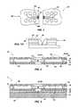
- FIGS. 1 and 1Arespectively show partial top and cross-sectional views of a portion of a conductive plane of a conventionally configured interposer substrate for a chip-scale, board-on-chip package;
- FIG. 2is a cross-sectional representation of an embodiment of a chip-scale, board-on-chip interposer substrate, or “redistribution element,” of the present invention, with at least two conductive planes that include conductive traces;
- FIG. 2Ais a cross-sectional representation of another embodiment of a redistribution element
- FIG. 3shows an embodiment of a semiconductor device package that includes an embodiment of a chip-scale, chip-on-board substrate that incorporates teachings of the present invention
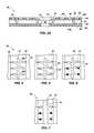
- FIGS. 4 through 7depict an embodiment of a process for fabricating a chip-scale, board-on-chip substrate with at least two conductive planes.
- FIGS. 1 and 1Aillustrate a portion of a state-of-the-art board-on-chip substrate 20 ′, which includes only one conductive plane 30 ′.
- Conductive plane 30 ′includes connection pads 32 ′ and conductive traces 34 ′ that extend laterally from connection pads 32 ′ to terminals 36 ′, to which solder balls or other discrete conductive structures (not shown) may be secured.
- four conductive traces 34 ′extend between a first pair of terminals 36 a ′ and 36 b ′.
- terminals 36 a ′ and 36 b ′must be spaced at least 360 ⁇ m apart from one another, which may be an undesirably large distance when restrictions on the area of substrate 20 ′ are considered in view of the large number of terminals that substrate 20 ′ must carry.
- a tighter design rulei.e., thinner, more closely spaced conductive traces
- the present inventionincludes an approach to accommodating additional circuit traces and their corresponding terminals, or pads, without tightening design rules.
- An embodiment of a chip-scale, board-on-chip substrate that incorporates teachings of the present inventionis shown in FIGS. 2 and 2A .
- the chip-scale, board-on-chip interposer substratemay be more generically referred to herein as a “redistribution element 20 .”
- the term “chip-scale”includes redistribution elements 20 that have dimensions that are about the same as or only slightly (e.g., up to 20%) larger than corresponding dimensions of the semiconductor device 10 ( FIG. 3 ) with which the redistribution elements 20 are assembled.
- a redistribution element according to the present inventionmay have state-of-the-art design rules (e.g., 40/40, in which conductive traces have maximum widths of 40 ⁇ m and are spaced a maximum of 40 ⁇ m apart from other conductive structures) or relaxed design rules (e.g., design rules that are greater than 40/40, or that allow for conductive trace widths and spacing that exceed 40 ⁇ m).
- state-of-the-art design rulese.g., 40/40, in which conductive traces have maximum widths of 40 ⁇ m and are spaced a maximum of 40 ⁇ m apart from other conductive structures
- relaxed design rulese.g., design rules that are greater than 40/40, or that allow for conductive trace widths and spacing that exceed 40 ⁇ m.
- Redistribution element 20includes a substrate 22 that is positioned between two conductive planes 30 and 40 and that electrically isolates overlapping portions of various elements (e.g., conductive traces, contact pads or terminals, etc.) within conductive planes 30 and 40 from one another.
- redistribution element 20includes insulation layers 26 and 28 , which may comprise known surface mount (S/M) materials, over conductive planes 30 and 40 , respectively.
- redistribution element 20includes an opening 24 , such as the depicted, elongate slot, that extends through the thickness of substrate 22 . Opening 24 may be defined by at least one interior peripheral edge 23 of substrate 22 .
- insulation layer 28is configured to be positioned adjacent to a bond pad-bearing surface 12 of a complementarily configured semiconductor device 10
- insulation layer 26is configured to be located at the exterior of a chip-scale package 1 that is formed when redistribution element 20 is assembled with semiconductor device 10 .
- Conductive plane 30is located closest to the exterior of chip-scale package 1 . Accordingly, conductive plane 30 is also referred to herein as an “outer conductive plane.” Conductive plane 30 includes a plurality of intermediate connection pads 32 and 42 , or “bond fingers.” Upon disposal of redistribution element 20 upon surface 12 of semiconductor device 10 , intermediate connection pads 32 and 42 are positioned laterally proximate to corresponding bond pads 14 of semiconductor device 10 . In the depicted embodiment, intermediate connection pads 32 and 42 are positioned adjacent to interior peripheral edge 23 of substrate 22 .
- conductive plane 30in addition to intermediate connection pads 32 and 42 , includes conductive traces 34 that extend laterally from intermediate connection pads 32 to redistributed bond pads 36 , which are also in conductive plane 30 . Conductive plane 30 also includes redistributed bond pads 46 that correspond to intermediate connection pads 42 .
- the lower, or base, conductive plane 40includes all or part of conductive traces 44 that correspond to connection pads 42 and redistributed bond pads 46 .
- conductive traces 44 or portions thereof in a second conductive plane 40conductive traces 34 of conductive plane 30 may be wider and/or spaced further distances apart from one another than the conductive traces 34 ′ of existing board-on-chip substrates 20 ′. Increased spacing between conductive traces 34 , 44 reduces inductance and decreases interference between adjacent electrical paths (i.e., between adjacent conductive traces 34 or 44 ).
- conductive traces 44provide routes for power (V ss ) and ground (V dd ) that are carried primarily by a separate conductive plane 40 than that (conductive plane 30 ) which carries signals.
- portions 44 a of the conductive traces 44may extend along conductive plane 40 .
- conductive traces 44may also include portions 44 b that are also located in, or extend along, conductive plane 30 to corresponding redistributed bond pads 46 .
- an entire conductive trace 44may be located in, or extend along, conductive plane 40 .
- a redistribution element 20may include a combination of these embodiments of conductive element portions 44 a / 44 b and conductive traces 44 .
- Each intermediate connection pad 42 in conductive plane 30communicates with its corresponding conductive trace 44 , or portion 44 a thereof, in conductive plane 40 by way of a conductive via 54 .
- each conductive via 54extends through an intermediate connection pad 42 to portion 44 a of conductive trace 44 at an opposite location on substrate 22 .
- Each conductive trace 44 ( FIG. 2 ), or portion 44 a thereof ( FIG. 2A ), in conductive plane 40communicates with corresponding redistributed bond pads 46 in conductive plane 30 by way of a conductive via 56 that extends from conductive plane 40 , through substrate 22 , and to conductive plane 30 . More specifically, each conductive via 56 extends directly to a corresponding redistributed bond pad 46 , as shown in FIG. 2 , or to a portion 44 b of conductive trace 44 that extends laterally across conductive plane 30 to the corresponding redistributed bond pad 46 , as illustrated by FIG. 2A .
- connection pads 32 , 42 and redistribution pads 36 , 46may have dimensions (e.g., diameters, side lengths, etc.) of about 300 ⁇ m, about 200 ⁇ m, or less than about 200 ⁇ m.
- Conductive traces 34 , 44 , and portions 44 a , 44 b of some embodiments of redistribution element 20may have widths of about 40 ⁇ m or greater, and may be spaced apart from one another and from other conductive features (e.g., redistribution pads 36 , 46 and/or connection pads 32 , 42 ) by a distance of at least about 40 ⁇ m.
- FIGS. 4 through 7an embodiment of a method for fabricating a redistribution element 20 of the present invention is illustrated and described.
- FIG. 4depicts a partially fabricated redistribution element 20 , which includes substrate 22 and conductive planes 30 and 40 ( FIGS. 2 through 3 ) and features (e.g., interconnected connection pad predecessors 32 P, 42 P, conductive traces 34 , 44 ( FIGS. 2 through 3 ), redistribution pads 36 , 46 ( FIGS. 2 through 3 ), etc.), and insulation layers 26 and 28 ( FIGS. 2 through 3 ).
- featurese.g., interconnected connection pad predecessors 32 P, 42 P, conductive traces 34 , 44 ( FIGS. 2 through 3 ), redistribution pads 36 , 46 ( FIGS. 2 through 3 ), etc.
- insulation layers 26 and 28FIGS. 2 through 3
- Redistribution element 20may be fabricated by processes that are known in the art.
- Redistribution element 20may comprise a conventional circuit board structure, which may include a substrate or substrate element 22 formed from a resin, such as BT resin, FR-4, or the like.
- conventional interposer substrate materialwhich may include a substrate 22 formed from a dielectric-coated semiconductor material, a thin layer of a ceramic material or glass, or the like, may comprise substrate 22 of redistribution element 20 .
- substrate 22may comprise a flexible (e.g., polyimide) film.
- Conductive planes 30 and 40may also be fabricated by known processes.
- a layer of conductive materialmay be formed both of the opposite major surfaces of substrate 22 , then patterned by known processes (e.g., mask and etch techniques, etc.) to define the conductive features of conductive planes 30 and 40 .
- substrate 22comprises a resin or flexible film
- conductive materiale.g., copper, aluminum, etc.
- a thin foilmay be applied and laminated to the major surfaces of substrate 22 .
- conductive planes 30 and 40may be deposited onto the opposite major surfaces of substrate 22 (e.g., by physical vapor deposition (PVD) processes, such as sputtering; chemical vapor deposition (CVD) processes; etc.).
- PVDphysical vapor deposition
- CVDchemical vapor deposition
- conductive planes 30 and 40may be fabricated by applying and laminating preformed, thin leads to the major surfaces of substrate 22 .
- Known printing techniquesmay also be used to form conductive planes 30 and 40 with features that are defined during application of a conductive material to the major surfaces of substrate 22 .
- insulation layers 26 and 28may be formed or applied to conductive planes 30 and 40 , respectively.
- one or both insulation layers 26 and 28may comprise a conventional surface mount (S/M) structure, such as an adhesive coated polyimide film.
- Insulation layer 26may be applied or formed over conductive plane 30 in such a way that a central area of conductive plane 30 , including an elongate bar 31 from which connection pad predecessors 32 P and 42 P extend, and underlying portions of a major surface of substrate 22 are exposed through insulation layer 26 .
- insulation layer 28may be foamed or applied in such a way that corresponding regions of the opposite side of substrate 22 , as well as features of conductive plane 40 on those regions of the opposite side of substrate 22 , are exposed.
- a via hole 50is formed through each intermediate connection pad 42 and an underlying location of substrate 22 .
- Via holes 50extend down to, but not necessarily through, conductive traces 44 ( FIG. 2 ) or portions 44 a thereof ( FIG. 2A ) that correspond to each connection pad 42 .
- via holes 50are being formed through intermediate connection pads 42 and underlying portions of substrate 22
- another set of via holes 52may be formed through portions 44 b of conductive traces 44 that extend laterally from redistributed bond pads 46 ( FIG. 2A ) or through redistributed bond pads 46 ( FIG. 2 ), as well as through portions of substrate 22 that underlie portions 44 b or redistributed bond pads 46 .
- via holes 52may expose, but do not necessarily extend into, conductive traces 44 .
- Such processesinclude, but are not limited to, mask and etch processes, laser drilling, mechanical drilling, and the like.
- conductive materialmay be introduced therein to form conductive vias 54 and 56 (conductive vias are shown in FIGS. 2 through 3 ), as illustrated in FIG. 6 .
- known processesincluding, but not limited to, electroless plating techniques and immersion plating techniques, may be used to introduce conductive material into via holes 50 and 52 .
- the resulting conductive vias 54enable electrical communication between connection pads 42 , which are in the outer conductive plane 30 ( FIGS. 2 through 3 ), and their corresponding conductive traces 44 ( FIG. 2 ), or portions 44 a thereof ( FIG. 2A ), in the base conductive plane 40 ( FIGS. 2 through 3 ).
- Conductive vias 56enable electric communication between conductive traces 44 , 44 a of the base conductive plane 40 and their corresponding redistributed bond pads 46 ( FIG. 2 ) or conductive trace portions 44 b ( FIG. 2A ) that are located in the upper conductive plane 30 .
- an opening 24such as a slot, may be formed through substrate 22 of redistribution element 20 .
- Known processesincluding, but not limited to, mechanical routing techniques, die-punch techniques, mask and etch techniques, and the like, may be used to form opening 24 .
- materialmay be removed from conductive plane 30 (e.g., from elongate bar 31 from which connection pad predecessors 32 P and 42 P extend and from pad predecessors 32 P and 42 P (FIG. 4 )), from substrate 22 , and from conductive plane 40 (e.g., from an elongate bar (not shown) from which conductive traces 44 extend).
- connection pads 32 and 42may be defined.
- Redistribution element 20may be part of a larger structure (e.g., a sheet, strip, full or partial wafer, etc.) that includes a plurality of redistribution elements.
- Semiconductor device 10may be a singulated semiconductor die, or a semiconductor die that remains part of a larger fabrication substrate (e.g., a full or partial wafer of semiconductor material, such as silicon, indium phosphide, gallium arsenide, etc.; a silicon-on-insulator (SOI) type substrate, such as silicon-on-ceramic (SOC), silicon-on-glass (SOG), silicon-on-sapphire (SOS); etc.) upon which a plurality of semiconductor devices have been fabricated and have not yet been cut, or singulated. While FIG., a larger fabrication substrate (e.g., a full or partial wafer of semiconductor material, such as silicon, indium phosphide, gallium arsenide, etc.; a silicon-on-insulator (SOI) type substrate, such as silicon-on-ceramic (SOC), silicon-on-glass (SOG), silicon-on-sapphire (SOS); etc.) upon which a plurality of semiconductor
- redistribution element 20with an embodiment of semiconductor device 10 that includes bond pads 14 that are arranged along a center line of semiconductor device 10
- other embodiments of redistribution elements 20may be configured for assembly with semiconductor devices with other arrangements of bond pads 14 , or connection patterns, including, but not limited to, peripherally located bond pads, bond pads arranged in an area array over a surface of the semiconductor device, and the like.
- Redistribution element 20is aligned over semiconductor device 10 in such a way that bond pads 14 of semiconductor device 10 are exposed at locations that are laterally adjacent and proximate to corresponding connection elements 32 , 42 of redistribution element 20 . In the depicted embodiment, bond pads 14 are exposed through opening 24 .
- Redistribution element 20may be adhered to surface 12 of semiconductor device 10 by any known, suitable technique.
- an adhesive element 29(not shown), such as a quantity of a suitable adhesive material or strip of material (e.g., polyimide, etc.) with adhesive material coating both major surfaces thereof, may secure insulation layer 28 of redistribution element 20 to surface 12 of semiconductor device 10 .
- an adhesive coating on an exposed surface of insulation layer 28may secure redistribution element 20 to surface 12 .
- bond pads 14 of semiconductor device 10 that are exposed through opening 24 of redistribution element 20may be electrically connected to corresponding connection pads 32 , 42 .
- intermediate conductive elements 60FIG. 1A
- intermediate conductive elements 60may comprise bond wires that are formed by known wire bonding processes.
- intermediate conductive elements 60may comprise leads, which may be carried by a flexible dielectric film (e.g., as is used in tape-automated bonding (TAB) processes).
- TABtape-automated bonding
- an encapsulant materiale.g., a quantity of glob-top encapsulant material, a lower viscosity encapsulant material, etc.
- an encapsulant materialmay be introduced onto intermediate conductive elements 60 to protect the same and to complete the assembly of a chip-scale package 1 according to the present invention.
- FIG. 3illustrates an embodiment in which connection pads 32 , 42 of an outer conductive plane 30 are connected to bond pads 14 of a semiconductor device 10
- connection pads, or bond fingersare part of a conductive plane located adjacent to a semiconductor device, may also be within the scope of the present invention.
Landscapes
- Engineering & Computer Science (AREA)
- Microelectronics & Electronic Packaging (AREA)
- Computer Hardware Design (AREA)
- Power Engineering (AREA)
- Physics & Mathematics (AREA)
- Condensed Matter Physics & Semiconductors (AREA)
- General Physics & Mathematics (AREA)
- Geometry (AREA)
- Production Of Multi-Layered Print Wiring Board (AREA)
- Structures For Mounting Electric Components On Printed Circuit Boards (AREA)
Abstract
Description
- This application is a continuation of U.S. patent application Ser. No. 12/106,845, filed Apr. 21, 2008, pending, the disclosure of which is hereby incorporated herein by this reference in its entirety.
- The present invention relates generally to substrates for chip-scale packages and, more specifically, to substrates with relaxed circuit design rules. In particular, the embodiments of the present invention relate to chip-scale “board-on-chip” (BOC), substrates with conductive traces located in two or more conductive planes, as well as to methods for designing and fabricating such substrates, to packaging methods, and to packages including the substrates.
- Printed circuit boards in the form of so-called “interposer substrates” have long been used as a primary medium for rerouting connection patterns of semiconductor devices, including in chip-scale packages (CSPs) for connection to higher-level packaging. The use of printed circuit boards is desirable since the processes for manufacturing them are well developed, inexpensive, and provide high yields. In addition, processes for packaging semiconductor devices with printed circuit boards have been refined over several decades of use. Further, printed circuit boards are themselves very reliable (i.e., they have low operational failure rates).
- Due to the ever-increasing device densities and speeds of state-of-the-art semiconductor devices, the number of bond pads on semiconductor devices also continue to increase. The overall dimensions of state-of-the-art semiconductor devices do not typically increase, however. The dimensions of the circuit board interposer substrates that are used in packaging such devices, particularly in chip-scale packages, are likewise limited. Consequently, an ever-increasing number of conductive traces and terminals must be arranged within the relatively fixed area of a printed circuit board interposer substrate.
- Until recently, increases in the numbers of conductive traces and terminals could be accommodated despite restrictions on the dimensions and areas of printed circuit board interposer substrates. As circuit design rules have approached the so-called “40/40” limit in which conductive traces have minimum widths of 40 μm and must be spaced at least 40 μm from each other and from other conductive structures, undesirable electrical issues, such as inductance between power and ground signals, have arisen. It is apparent that these problems would be magnified with even tighter design rules (i.e., conductive traces with widths of less than 40 μm that are closer than 40 μm to one another and to other conductive structures).
- Accordingly, there are needs for interposer substrate design and manufacture processes, as well as for interposer substrates, that accommodate increased numbers of circuits without further tightened design rules.
- In the drawings:
FIGS. 1 and 1A respectively show partial top and cross-sectional views of a portion of a conductive plane of a conventionally configured interposer substrate for a chip-scale, board-on-chip package;FIG. 2 is a cross-sectional representation of an embodiment of a chip-scale, board-on-chip interposer substrate, or “redistribution element,” of the present invention, with at least two conductive planes that include conductive traces;FIG. 2A is a cross-sectional representation of another embodiment of a redistribution element;FIG. 3 shows an embodiment of a semiconductor device package that includes an embodiment of a chip-scale, chip-on-board substrate that incorporates teachings of the present invention; andFIGS. 4 through 7 depict an embodiment of a process for fabricating a chip-scale, board-on-chip substrate with at least two conductive planes.FIGS. 1 and 1A illustrate a portion of a state-of-the-art board-on-chip substrate 20′, which includes only oneconductive plane 30′.Conductive plane 30′ includesconnection pads 32′ andconductive traces 34′ that extend laterally fromconnection pads 32′ toterminals 36′, to which solder balls or other discrete conductive structures (not shown) may be secured. As shown, fourconductive traces 34′ extend between a first pair ofterminals 36a′ and36b′. With a 40/40 design rule, which is the current state of the art,terminals 36a′ and36b′ must be spaced at least 360 μm apart from one another, which may be an undesirably large distance when restrictions on the area ofsubstrate 20′ are considered in view of the large number of terminals thatsubstrate 20′ must carry. A tighter design rule (i.e., thinner, more closely spaced conductive traces) would undesirably generate additional inductance and would also likely result in decreased product yields.- The present invention includes an approach to accommodating additional circuit traces and their corresponding terminals, or pads, without tightening design rules. An embodiment of a chip-scale, board-on-chip substrate that incorporates teachings of the present invention is shown in
FIGS. 2 and 2A . For the sake of simplicity, the chip-scale, board-on-chip interposer substrate may be more generically referred to herein as a “redistribution element 20.” As used herein, the term “chip-scale” includesredistribution elements 20 that have dimensions that are about the same as or only slightly (e.g., up to 20%) larger than corresponding dimensions of the semiconductor device10 (FIG. 3 ) with which theredistribution elements 20 are assembled. In various embodiments, a redistribution element according to the present invention may have state-of-the-art design rules (e.g., 40/40, in which conductive traces have maximum widths of 40 μm and are spaced a maximum of 40 μm apart from other conductive structures) or relaxed design rules (e.g., design rules that are greater than 40/40, or that allow for conductive trace widths and spacing that exceed 40 μm). Redistribution element 20 includes asubstrate 22 that is positioned between twoconductive planes conductive planes redistribution element 20 includesinsulation layers conductive planes redistribution element 20 includes anopening 24, such as the depicted, elongate slot, that extends through the thickness ofsubstrate 22.Opening 24 may be defined by at least one interiorperipheral edge 23 ofsubstrate 22.- Turning now to
FIG. 3 ,insulation layer 28 is configured to be positioned adjacent to a bond pad-bearingsurface 12 of a complementarily configuredsemiconductor device 10, whileinsulation layer 26 is configured to be located at the exterior of a chip-scale package 1 that is formed whenredistribution element 20 is assembled withsemiconductor device 10. - As shown,
conductive plane 30 is located closest to the exterior of chip-scale package 1. Accordingly,conductive plane 30 is also referred to herein as an “outer conductive plane.”Conductive plane 30 includes a plurality ofintermediate connection pads redistribution element 20 uponsurface 12 ofsemiconductor device 10,intermediate connection pads corresponding bond pads 14 ofsemiconductor device 10. In the depicted embodiment,intermediate connection pads peripheral edge 23 ofsubstrate 22. - With continued reference to
FIGS. 2 through 3 , in addition tointermediate connection pads conductive plane 30 includesconductive traces 34 that extend laterally fromintermediate connection pads 32 to redistributedbond pads 36, which are also inconductive plane 30.Conductive plane 30 also includesredistributed bond pads 46 that correspond tointermediate connection pads 42. - The lower, or base,
conductive plane 40 includes all or part ofconductive traces 44 that correspond toconnection pads 42 andredistributed bond pads 46. By includingconductive traces 44 or portions thereof in a secondconductive plane 40,conductive traces 34 ofconductive plane 30 may be wider and/or spaced further distances apart from one another than theconductive traces 34′ of existing board-on-chip substrates 20′. Increased spacing betweenconductive traces conductive traces 34 or44). In some embodiments,conductive traces 44 provide routes for power (Vss) and ground (Vdd) that are carried primarily by a separateconductive plane 40 than that (conductive plane30) which carries signals. - In the embodiment shown in
FIG. 2A ,portions 44aof the conductive traces44 (FIG. 2 ) that connectintermediate connection pads 42 to their correspondingredistributed bond pads 46 may extend alongconductive plane 40. In these embodiments,conductive traces 44 may also includeportions 44bthat are also located in, or extend along,conductive plane 30 to correspondingredistributed bond pads 46. In other embodiments, as shown inFIG. 2 , an entireconductive trace 44 may be located in, or extend along,conductive plane 40. Of course, aredistribution element 20 according to the present invention may include a combination of these embodiments ofconductive element portions 44a/44bandconductive traces 44. - Each
intermediate connection pad 42 inconductive plane 30 communicates with its correspondingconductive trace 44, orportion 44athereof, inconductive plane 40 by way of a conductive via54. In the illustrated embodiments, each conductive via54 extends through anintermediate connection pad 42 toportion 44aofconductive trace 44 at an opposite location onsubstrate 22. - Each conductive trace44 (
FIG. 2 ), orportion 44athereof (FIG. 2A ), inconductive plane 40 communicates with correspondingredistributed bond pads 46 inconductive plane 30 by way of a conductive via56 that extends fromconductive plane 40, throughsubstrate 22, and toconductive plane 30. More specifically, each conductive via56 extends directly to a correspondingredistributed bond pad 46, as shown inFIG. 2 , or to aportion 44bofconductive trace 44 that extends laterally acrossconductive plane 30 to the correspondingredistributed bond pad 46, as illustrated byFIG. 2A . - In some embodiments,
connection pads redistribution pads portions redistribution element 20 may have widths of about 40 μm or greater, and may be spaced apart from one another and from other conductive features (e.g.,redistribution pads connection pads 32,42) by a distance of at least about 40 μm. - Turning now to
FIGS. 4 through 7 , an embodiment of a method for fabricating aredistribution element 20 of the present invention is illustrated and described. FIG. 4 depicts a partially fabricatedredistribution element 20, which includessubstrate 22 andconductive planes 30 and40 (FIGS. 2 through 3 ) and features (e.g., interconnectedconnection pad predecessors conductive traces 34,44 (FIGS. 2 through 3 ),redistribution pads 36,46 (FIGS. 2 through 3 ), etc.), andinsulation layers 26 and28 (FIGS. 2 through 3 ).Redistribution element 20 may be fabricated by processes that are known in the art.Redistribution element 20 may comprise a conventional circuit board structure, which may include a substrate orsubstrate element 22 formed from a resin, such as BT resin, FR-4, or the like. Alternatively, conventional interposer substrate material, which may include asubstrate 22 formed from a dielectric-coated semiconductor material, a thin layer of a ceramic material or glass, or the like, may comprisesubstrate 22 ofredistribution element 20. In other embodiments,substrate 22 may comprise a flexible (e.g., polyimide) film.Conductive planes 30 and40 (FIGS. 2 through 3 ) may also be fabricated by known processes. In some embodiments, a layer of conductive material may be formed both of the opposite major surfaces ofsubstrate 22, then patterned by known processes (e.g., mask and etch techniques, etc.) to define the conductive features ofconductive planes substrate 22 comprises a resin or flexible film, conductive material (e.g., copper, aluminum, etc.) in the form of a thin foil may be applied and laminated to the major surfaces ofsubstrate 22. In embodiments wheresubstrate 22 comprises an interposer substrate material, the material ofconductive planes conductive planes substrate 22. Known printing techniques may also be used to formconductive planes substrate 22.- Once
conductive planes substrate 22, insulation layers26 and28 (insulation layer 28 is shown inFIGS. 2 through 3 ) may be formed or applied toconductive planes Insulation layer 26 may be applied or formed overconductive plane 30 in such a way that a central area ofconductive plane 30, including anelongate bar 31 from whichconnection pad predecessors substrate 22 are exposed throughinsulation layer 26. Similarly,insulation layer 28 may be foamed or applied in such a way that corresponding regions of the opposite side ofsubstrate 22, as well as features ofconductive plane 40 on those regions of the opposite side ofsubstrate 22, are exposed. - As shown in
FIG. 5 , a viahole 50 is formed through eachintermediate connection pad 42 and an underlying location ofsubstrate 22. Viaholes 50 extend down to, but not necessarily through, conductive traces44 (FIG. 2 ) orportions 44athereof (FIG. 2A ) that correspond to eachconnection pad 42. - While via
holes 50 are being formed throughintermediate connection pads 42 and underlying portions ofsubstrate 22, another set of via holes52 (FIGS. 2 through 3 ) may be formed throughportions 44bofconductive traces 44 that extend laterally from redistributed bond pads46 (FIG. 2A ) or through redistributed bond pads46 (FIG. 2 ), as well as through portions ofsubstrate 22 that underlieportions 44bor redistributedbond pads 46. Like viaholes 50, viaholes 52 may expose, but do not necessarily extend into, conductive traces44. - Known processes may be used to form via
holes - Once via
holes conductive vias 54 and56 (conductive vias are shown inFIGS. 2 through 3 ), as illustrated inFIG. 6 . In various embodiments, known processes, including, but not limited to, electroless plating techniques and immersion plating techniques, may be used to introduce conductive material into viaholes - The resulting
conductive vias 54 enable electrical communication betweenconnection pads 42, which are in the outer conductive plane30 (FIGS. 2 through 3 ), and their corresponding conductive traces44 (FIG. 2 ), orportions 44athereof (FIG. 2A ), in the base conductive plane40 (FIGS. 2 through 3 ).Conductive vias 56 enable electric communication betweenconductive traces conductive plane 40 and their corresponding redistributed bond pads46 (FIG. 2 ) orconductive trace portions 44b(FIG. 2A ) that are located in the upperconductive plane 30. - Turning to
FIG. 7 , in some embodiments, anopening 24, such as a slot, may be formed throughsubstrate 22 ofredistribution element 20. Known processes, including, but not limited to, mechanical routing techniques, die-punch techniques, mask and etch techniques, and the like, may be used to formopening 24. As opening24 is formed, material may be removed from conductive plane30 (e.g., fromelongate bar 31 from whichconnection pad predecessors pad predecessors substrate 22, and from conductive plane40 (e.g., from an elongate bar (not shown) from which conductive traces44 extend). As material is removed fromconductive plane 30,connection pads - With returned reference to
FIG. 3 , an embodiment of a process for assembling aredistribution element 20 with asemiconductor device 10 is described.Redistribution element 20 may be part of a larger structure (e.g., a sheet, strip, full or partial wafer, etc.) that includes a plurality of redistribution elements.Semiconductor device 10 may be a singulated semiconductor die, or a semiconductor die that remains part of a larger fabrication substrate (e.g., a full or partial wafer of semiconductor material, such as silicon, indium phosphide, gallium arsenide, etc.; a silicon-on-insulator (SOI) type substrate, such as silicon-on-ceramic (SOC), silicon-on-glass (SOG), silicon-on-sapphire (SOS); etc.) upon which a plurality of semiconductor devices have been fabricated and have not yet been cut, or singulated. WhileFIG. 3 depicts the assembly of aredistribution element 20 with an embodiment ofsemiconductor device 10 that includesbond pads 14 that are arranged along a center line ofsemiconductor device 10, other embodiments ofredistribution elements 20 that incorporate teachings of the present invention may be configured for assembly with semiconductor devices with other arrangements ofbond pads 14, or connection patterns, including, but not limited to, peripherally located bond pads, bond pads arranged in an area array over a surface of the semiconductor device, and the like. Redistribution element 20 is aligned oversemiconductor device 10 in such a way thatbond pads 14 ofsemiconductor device 10 are exposed at locations that are laterally adjacent and proximate tocorresponding connection elements redistribution element 20. In the depicted embodiment,bond pads 14 are exposed throughopening 24.Redistribution element 20 may be adhered to surface12 ofsemiconductor device 10 by any known, suitable technique. In some embodiments, an adhesive element29 (not shown), such as a quantity of a suitable adhesive material or strip of material (e.g., polyimide, etc.) with adhesive material coating both major surfaces thereof, may secureinsulation layer 28 ofredistribution element 20 to surface12 ofsemiconductor device 10. In other embodiments, an adhesive coating on an exposed surface ofinsulation layer 28 may secureredistribution element 20 to surface12.- Once
redistribution element 20 andsemiconductor device 10 have been assembled and secured to one another,bond pads 14 ofsemiconductor device 10 that are exposed through opening24 ofredistribution element 20 may be electrically connected tocorresponding connection pads FIG. 1A ) may be formed or placed betweenbond pads 14 and theircorresponding connection pads conductive elements 60 may comprise bond wires that are formed by known wire bonding processes. In other embodiments, intermediateconductive elements 60 may comprise leads, which may be carried by a flexible dielectric film (e.g., as is used in tape-automated bonding (TAB) processes). - Additionally, an encapsulant material (e.g., a quantity of glob-top encapsulant material, a lower viscosity encapsulant material, etc.) may be introduced onto intermediate
conductive elements 60 to protect the same and to complete the assembly of a chip-scale package 1 according to the present invention. - While
FIG. 3 illustrates an embodiment in whichconnection pads conductive plane 30 are connected to bondpads 14 of asemiconductor device 10, other embodiments, including embodiments in which connection pads, or bond fingers, are part of a conductive plane located adjacent to a semiconductor device, may also be within the scope of the present invention. - Although the foregoing description contains many specifics, these should not be construed as limiting the scope of the present invention, but merely as providing illustrations of some embodiments. Similarly, other embodiments of the invention may be devised which do not exceed the scope of the present invention. Features from different embodiments may be employed in combination. The scope of the invention is, therefore, indicated and limited only by the appended claims and their legal equivalents, rather than by the foregoing description. All additions, deletions and modifications to the invention as disclosed herein which fall within the meaning and scope of the claims are to be embraced thereby.
Claims (20)
Priority Applications (3)
| Application Number | Priority Date | Filing Date | Title |
|---|---|---|---|
| US13/181,197US8288859B2 (en) | 2008-03-03 | 2011-07-12 | Semiconductor device packages including a semiconductor device and a redistribution element |
| US13/612,333US8486825B2 (en) | 2008-03-03 | 2012-09-12 | Methods of forming semiconductor device packages including a semiconductor device and a redistribution element, methods of forming redistribution elements and methods for packaging semiconductor devices |
| US13/933,294US8749050B2 (en) | 2008-03-03 | 2013-07-02 | Redistribution elements and semiconductor device packages including semiconductor devices and redistribution elements |
Applications Claiming Priority (4)
| Application Number | Priority Date | Filing Date | Title |
|---|---|---|---|
| SG200801773-3ASG155096A1 (en) | 2008-03-03 | 2008-03-03 | Board-on-chip type substrates with conductive traces in multiple planes, semiconductor device packages including such substrates, and associated methods |
| SG200801773-3 | 2008-03-03 | ||
| US12/106,845US8030751B2 (en) | 2008-03-03 | 2008-04-21 | Board-on-chip type substrates with conductive traces in multiple planes and semiconductor device packages including such substrates |
| US13/181,197US8288859B2 (en) | 2008-03-03 | 2011-07-12 | Semiconductor device packages including a semiconductor device and a redistribution element |
Related Parent Applications (1)
| Application Number | Title | Priority Date | Filing Date |
|---|---|---|---|
| US12/106,845ContinuationUS8030751B2 (en) | 2008-03-03 | 2008-04-21 | Board-on-chip type substrates with conductive traces in multiple planes and semiconductor device packages including such substrates |
Related Child Applications (2)
| Application Number | Title | Priority Date | Filing Date |
|---|---|---|---|
| US13/612,333ContinuationUS8486825B2 (en) | 2008-03-03 | 2012-09-12 | Methods of forming semiconductor device packages including a semiconductor device and a redistribution element, methods of forming redistribution elements and methods for packaging semiconductor devices |
| US13/612,233ContinuationUS8994454B2 (en) | 2011-11-22 | 2012-09-12 | Amplifier circuit |
Publications (2)
| Publication Number | Publication Date |
|---|---|
| US20110266696A1true US20110266696A1 (en) | 2011-11-03 |
| US8288859B2 US8288859B2 (en) | 2012-10-16 |
Family
ID=41012539
Family Applications (4)
| Application Number | Title | Priority Date | Filing Date |
|---|---|---|---|
| US12/106,845Active2029-07-03US8030751B2 (en) | 2008-03-03 | 2008-04-21 | Board-on-chip type substrates with conductive traces in multiple planes and semiconductor device packages including such substrates |
| US13/181,197ActiveUS8288859B2 (en) | 2008-03-03 | 2011-07-12 | Semiconductor device packages including a semiconductor device and a redistribution element |
| US13/612,333ActiveUS8486825B2 (en) | 2008-03-03 | 2012-09-12 | Methods of forming semiconductor device packages including a semiconductor device and a redistribution element, methods of forming redistribution elements and methods for packaging semiconductor devices |
| US13/933,294ActiveUS8749050B2 (en) | 2008-03-03 | 2013-07-02 | Redistribution elements and semiconductor device packages including semiconductor devices and redistribution elements |
Family Applications Before (1)
| Application Number | Title | Priority Date | Filing Date |
|---|---|---|---|
| US12/106,845Active2029-07-03US8030751B2 (en) | 2008-03-03 | 2008-04-21 | Board-on-chip type substrates with conductive traces in multiple planes and semiconductor device packages including such substrates |
Family Applications After (2)
| Application Number | Title | Priority Date | Filing Date |
|---|---|---|---|
| US13/612,333ActiveUS8486825B2 (en) | 2008-03-03 | 2012-09-12 | Methods of forming semiconductor device packages including a semiconductor device and a redistribution element, methods of forming redistribution elements and methods for packaging semiconductor devices |
| US13/933,294ActiveUS8749050B2 (en) | 2008-03-03 | 2013-07-02 | Redistribution elements and semiconductor device packages including semiconductor devices and redistribution elements |
Country Status (2)
| Country | Link |
|---|---|
| US (4) | US8030751B2 (en) |
| SG (1) | SG155096A1 (en) |
Cited By (1)
| Publication number | Priority date | Publication date | Assignee | Title |
|---|---|---|---|---|
| US8486825B2 (en) | 2008-03-03 | 2013-07-16 | Micron Technology, Inc. | Methods of forming semiconductor device packages including a semiconductor device and a redistribution element, methods of forming redistribution elements and methods for packaging semiconductor devices |
Families Citing this family (3)
| Publication number | Priority date | Publication date | Assignee | Title |
|---|---|---|---|---|
| US20140062916A1 (en)* | 2012-08-28 | 2014-03-06 | Lg Display Co., Ltd. | Touch panel and method of manufacturing the same and display device using the same |
| CN104979460A (en)* | 2014-04-03 | 2015-10-14 | 美丽微半导体股份有限公司 | Flip-chip LED element with built-in voltage-stabilizing chip |
| KR102654925B1 (en) | 2016-06-21 | 2024-04-05 | 삼성디스플레이 주식회사 | Display apparatus and manufacturing method of the same |
Citations (6)
| Publication number | Priority date | Publication date | Assignee | Title |
|---|---|---|---|---|
| US4622058A (en)* | 1984-06-22 | 1986-11-11 | International Business Machines Corporation | Formation of a multi-layer glass-metallized structure formed on and interconnected to multi-layered-metallized ceramic substrate |
| US20080050901A1 (en)* | 2006-08-23 | 2008-02-28 | Micron Technology, Inc. | Packaged microelectronic devices and methods for manufacturing packaged microelectronic devices |
| US20080191354A1 (en)* | 2005-03-23 | 2008-08-14 | Endicott Interconnect Technologies, Inc. | Circuitized substrate with p-aramid dielectric layers and method of making same |
| US20090053858A1 (en)* | 2007-08-24 | 2009-02-26 | Samsung Electronics Co., Ltd. | Method of manufacturing semiconductor package using redistribution substrate |
| US7524703B2 (en)* | 2001-10-26 | 2009-04-28 | Entorian Technologies, Lp | Integrated circuit stacking system and method |
| US7719098B2 (en)* | 2001-10-26 | 2010-05-18 | Entorian Technologies Lp | Stacked modules and method |
Family Cites Families (32)
| Publication number | Priority date | Publication date | Assignee | Title |
|---|---|---|---|---|
| US4434321A (en)* | 1981-02-09 | 1984-02-28 | International Computers Limited | Multilayer printed circuit boards |
| US4613891A (en)* | 1984-02-17 | 1986-09-23 | At&T Bell Laboratories | Packaging microminiature devices |
| US4700473A (en)* | 1986-01-03 | 1987-10-20 | Motorola Inc. | Method of making an ultra high density pad array chip carrier |
| JP2988075B2 (en)* | 1991-10-19 | 1999-12-06 | 日本電気株式会社 | Semiconductor device |
| TW276356B (en)* | 1994-06-24 | 1996-05-21 | Ibm | |
| EP0818752A2 (en)* | 1996-07-08 | 1998-01-14 | Fela Holding AG | Inlet for chipcards |
| SE511377C2 (en)* | 1996-12-19 | 1999-09-20 | Ericsson Telefon Ab L M | via structure |
| US6598291B2 (en)* | 1998-03-20 | 2003-07-29 | Viasystems, Inc. | Via connector and method of making same |
| SG86345A1 (en)* | 1998-05-14 | 2002-02-19 | Matsushita Electric Industrial Co Ltd | Circuit board and method of manufacturing the same |
| US6965165B2 (en)* | 1998-12-21 | 2005-11-15 | Mou-Shiung Lin | Top layers of metal for high performance IC's |
| JP3798597B2 (en) | 1999-11-30 | 2006-07-19 | 富士通株式会社 | Semiconductor device |
| KR100421774B1 (en) | 1999-12-16 | 2004-03-10 | 앰코 테크놀로지 코리아 주식회사 | semiconductor package and its manufacturing method |
| US6707140B1 (en) | 2000-05-09 | 2004-03-16 | National Semiconductor Corporation | Arrayable, scaleable, and stackable molded package configuration |
| US6847105B2 (en)* | 2001-09-21 | 2005-01-25 | Micron Technology, Inc. | Bumping technology in stacked die configurations |
| JP3666591B2 (en)* | 2002-02-01 | 2005-06-29 | 株式会社トッパンNecサーキットソリューションズ | Manufacturing method of semiconductor chip mounting substrate |
| US6710246B1 (en) | 2002-08-02 | 2004-03-23 | National Semiconductor Corporation | Apparatus and method of manufacturing a stackable package for a semiconductor device |
| TWI220163B (en)* | 2003-04-24 | 2004-08-11 | Ind Tech Res Inst | Manufacturing method of high-conductivity nanometer thin-film probe card |
| US6853064B2 (en)* | 2003-05-12 | 2005-02-08 | Micron Technology, Inc. | Semiconductor component having stacked, encapsulated dice |
| US7422930B2 (en)* | 2004-03-02 | 2008-09-09 | Infineon Technologies Ag | Integrated circuit with re-route layer and stacked die assembly |
| US7015587B1 (en) | 2004-09-07 | 2006-03-21 | National Semiconductor Corporation | Stacked die package for semiconductor devices |
| US7030317B1 (en) | 2005-04-13 | 2006-04-18 | Delphi Technologies, Inc. | Electronic assembly with stacked integrated circuit die |
| KR100652519B1 (en)* | 2005-07-18 | 2006-12-01 | 삼성전자주식회사 | Tape wiring board with dual metal layer and chip on film package |
| JP2007184414A (en)* | 2006-01-06 | 2007-07-19 | Matsushita Electric Ind Co Ltd | Semiconductor device mounting substrate, semiconductor device and electronic apparatus |
| TWI294654B (en) | 2006-04-24 | 2008-03-11 | Siliconware Precision Industries Co Ltd | Stack structure for semiconductor package and method for fabricating the same |
| JP2008016508A (en)* | 2006-07-03 | 2008-01-24 | Nec Electronics Corp | Semiconductor device and its fabrication process |
| US7683741B2 (en)* | 2007-11-07 | 2010-03-23 | Intel Corporation | Package for suppressing spurious resonance in an FBAR |
| US7928550B2 (en)* | 2007-11-08 | 2011-04-19 | Texas Instruments Incorporated | Flexible interposer for stacking semiconductor chips and connecting same to substrate |
| US20090212428A1 (en)* | 2008-02-22 | 2009-08-27 | Advanced Chip Engineering Technology Inc. | Re-distribution conductive line structure and the method of forming the same |
| SG155096A1 (en) | 2008-03-03 | 2009-09-30 | Micron Technology Inc | Board-on-chip type substrates with conductive traces in multiple planes, semiconductor device packages including such substrates, and associated methods |
| KR101209980B1 (en)* | 2010-12-09 | 2012-12-07 | 주식회사 네패스 | Semiconductor package and fabrication method thereof |
| US8466544B2 (en)* | 2011-02-25 | 2013-06-18 | Stats Chippac, Ltd. | Semiconductor device and method of forming interposer and opposing build-up interconnect structure with connecting conductive TMV for electrical interconnect of Fo-WLCSP |
| US8901755B2 (en)* | 2012-03-20 | 2014-12-02 | Stats Chippac, Ltd. | Semiconductor device and method of forming conductive layer over metal substrate for electrical interconnect of semiconductor die |
- 2008
- 2008-03-03SGSG200801773-3Apatent/SG155096A1/enunknown
- 2008-04-21USUS12/106,845patent/US8030751B2/enactiveActive
- 2011
- 2011-07-12USUS13/181,197patent/US8288859B2/enactiveActive
- 2012
- 2012-09-12USUS13/612,333patent/US8486825B2/enactiveActive
- 2013
- 2013-07-02USUS13/933,294patent/US8749050B2/enactiveActive
Patent Citations (6)
| Publication number | Priority date | Publication date | Assignee | Title |
|---|---|---|---|---|
| US4622058A (en)* | 1984-06-22 | 1986-11-11 | International Business Machines Corporation | Formation of a multi-layer glass-metallized structure formed on and interconnected to multi-layered-metallized ceramic substrate |
| US7524703B2 (en)* | 2001-10-26 | 2009-04-28 | Entorian Technologies, Lp | Integrated circuit stacking system and method |
| US7719098B2 (en)* | 2001-10-26 | 2010-05-18 | Entorian Technologies Lp | Stacked modules and method |
| US20080191354A1 (en)* | 2005-03-23 | 2008-08-14 | Endicott Interconnect Technologies, Inc. | Circuitized substrate with p-aramid dielectric layers and method of making same |
| US20080050901A1 (en)* | 2006-08-23 | 2008-02-28 | Micron Technology, Inc. | Packaged microelectronic devices and methods for manufacturing packaged microelectronic devices |
| US20090053858A1 (en)* | 2007-08-24 | 2009-02-26 | Samsung Electronics Co., Ltd. | Method of manufacturing semiconductor package using redistribution substrate |
Cited By (2)
| Publication number | Priority date | Publication date | Assignee | Title |
|---|---|---|---|---|
| US8486825B2 (en) | 2008-03-03 | 2013-07-16 | Micron Technology, Inc. | Methods of forming semiconductor device packages including a semiconductor device and a redistribution element, methods of forming redistribution elements and methods for packaging semiconductor devices |
| US8749050B2 (en) | 2008-03-03 | 2014-06-10 | Micron Technology, Inc. | Redistribution elements and semiconductor device packages including semiconductor devices and redistribution elements |
Also Published As
| Publication number | Publication date |
|---|---|
| US8030751B2 (en) | 2011-10-04 |
| US20130292810A1 (en) | 2013-11-07 |
| US8288859B2 (en) | 2012-10-16 |
| US8486825B2 (en) | 2013-07-16 |
| SG155096A1 (en) | 2009-09-30 |
| US8749050B2 (en) | 2014-06-10 |
| US20090218677A1 (en) | 2009-09-03 |
| US20130059419A1 (en) | 2013-03-07 |
Similar Documents
| Publication | Publication Date | Title |
|---|---|---|
| US7843068B2 (en) | Semiconductor chip and method of manufacturing the same | |
| US7452751B2 (en) | Semiconductor device and method of manufacturing the same | |
| CN101548378B (en) | Semiconductor device and manufacturing method thereof | |
| US7372131B2 (en) | Routing element for use in semiconductor device assemblies | |
| US20090085192A1 (en) | Packaging substrate structure having semiconductor chip embedded therein and fabricating method thereof | |
| CN104916623B (en) | Semiconductor package and method of manufacturing semiconductor package substrate | |
| US8178790B2 (en) | Interposer and method for manufacturing interposer | |
| US20150245485A1 (en) | Printed wiring board and method for manufacturing printed wiring board | |
| US11329007B2 (en) | Wiring structure and method for manufacturing the same | |
| US20250157947A1 (en) | Wiring structure and method for manufacturing the same | |
| US10117340B2 (en) | Manufacturing method of package substrate with metal on conductive portions | |
| US8749050B2 (en) | Redistribution elements and semiconductor device packages including semiconductor devices and redistribution elements | |
| US20050252683A1 (en) | Circuit substrate and method of manufacturing plated through slot thereon | |
| US20200279804A1 (en) | Wiring structure and method for manufacturing the same | |
| US9252132B2 (en) | Semiconductor device and semiconductor module | |
| US6465890B1 (en) | Integrated circuit package having offset segmentation of package power and/or ground planes and methods for reducing delamination in integrated circuit packages | |
| US9171795B2 (en) | Integrated circuit packaging system with embedded component and method of manufacture thereof | |
| US7345363B2 (en) | Semiconductor device with a rewiring level and method for producing the same | |
| CN112825310A (en) | Packaging structure and flexible integrated packaging method of ultrathin chip | |
| WO2015001662A1 (en) | Semiconductor device and manufacturing method for same | |
| US8125074B2 (en) | Laminated substrate for an integrated circuit BGA package and printed circuit boards | |
| JP6063785B2 (en) | Circuit board, method for manufacturing circuit board | |
| CN107785332A (en) | Semiconductor structure | |
| JP2005101186A (en) | Multilayer semiconductor integrated circuit | |
| US11894293B2 (en) | Circuit structure and electronic structure |
Legal Events
| Date | Code | Title | Description |
|---|---|---|---|
| FEPP | Fee payment procedure | Free format text:PAYOR NUMBER ASSIGNED (ORIGINAL EVENT CODE: ASPN); ENTITY STATUS OF PATENT OWNER: LARGE ENTITY | |
| STCF | Information on status: patent grant | Free format text:PATENTED CASE | |
| FPAY | Fee payment | Year of fee payment:4 | |
| AS | Assignment | Owner name:U.S. BANK NATIONAL ASSOCIATION, AS COLLATERAL AGENT, CALIFORNIA Free format text:SECURITY INTEREST;ASSIGNOR:MICRON TECHNOLOGY, INC.;REEL/FRAME:038669/0001 Effective date:20160426 Owner name:U.S. BANK NATIONAL ASSOCIATION, AS COLLATERAL AGEN Free format text:SECURITY INTEREST;ASSIGNOR:MICRON TECHNOLOGY, INC.;REEL/FRAME:038669/0001 Effective date:20160426 | |
| AS | Assignment | Owner name:MORGAN STANLEY SENIOR FUNDING, INC., AS COLLATERAL AGENT, MARYLAND Free format text:PATENT SECURITY AGREEMENT;ASSIGNOR:MICRON TECHNOLOGY, INC.;REEL/FRAME:038954/0001 Effective date:20160426 Owner name:MORGAN STANLEY SENIOR FUNDING, INC., AS COLLATERAL Free format text:PATENT SECURITY AGREEMENT;ASSIGNOR:MICRON TECHNOLOGY, INC.;REEL/FRAME:038954/0001 Effective date:20160426 | |
| AS | Assignment | Owner name:U.S. BANK NATIONAL ASSOCIATION, AS COLLATERAL AGENT, CALIFORNIA Free format text:CORRECTIVE ASSIGNMENT TO CORRECT THE REPLACE ERRONEOUSLY FILED PATENT #7358718 WITH THE CORRECT PATENT #7358178 PREVIOUSLY RECORDED ON REEL 038669 FRAME 0001. ASSIGNOR(S) HEREBY CONFIRMS THE SECURITY INTEREST;ASSIGNOR:MICRON TECHNOLOGY, INC.;REEL/FRAME:043079/0001 Effective date:20160426 Owner name:U.S. BANK NATIONAL ASSOCIATION, AS COLLATERAL AGEN Free format text:CORRECTIVE ASSIGNMENT TO CORRECT THE REPLACE ERRONEOUSLY FILED PATENT #7358718 WITH THE CORRECT PATENT #7358178 PREVIOUSLY RECORDED ON REEL 038669 FRAME 0001. ASSIGNOR(S) HEREBY CONFIRMS THE SECURITY INTEREST;ASSIGNOR:MICRON TECHNOLOGY, INC.;REEL/FRAME:043079/0001 Effective date:20160426 | |
| AS | Assignment | Owner name:JPMORGAN CHASE BANK, N.A., AS COLLATERAL AGENT, ILLINOIS Free format text:SECURITY INTEREST;ASSIGNORS:MICRON TECHNOLOGY, INC.;MICRON SEMICONDUCTOR PRODUCTS, INC.;REEL/FRAME:047540/0001 Effective date:20180703 Owner name:JPMORGAN CHASE BANK, N.A., AS COLLATERAL AGENT, IL Free format text:SECURITY INTEREST;ASSIGNORS:MICRON TECHNOLOGY, INC.;MICRON SEMICONDUCTOR PRODUCTS, INC.;REEL/FRAME:047540/0001 Effective date:20180703 | |
| AS | Assignment | Owner name:MICRON TECHNOLOGY, INC., IDAHO Free format text:RELEASE BY SECURED PARTY;ASSIGNOR:U.S. BANK NATIONAL ASSOCIATION, AS COLLATERAL AGENT;REEL/FRAME:047243/0001 Effective date:20180629 | |
| AS | Assignment | Owner name:MICRON TECHNOLOGY, INC., IDAHO Free format text:RELEASE BY SECURED PARTY;ASSIGNOR:MORGAN STANLEY SENIOR FUNDING, INC., AS COLLATERAL AGENT;REEL/FRAME:050937/0001 Effective date:20190731 | |
| AS | Assignment | Owner name:MICRON TECHNOLOGY, INC., IDAHO Free format text:RELEASE BY SECURED PARTY;ASSIGNOR:JPMORGAN CHASE BANK, N.A., AS COLLATERAL AGENT;REEL/FRAME:051028/0001 Effective date:20190731 Owner name:MICRON SEMICONDUCTOR PRODUCTS, INC., IDAHO Free format text:RELEASE BY SECURED PARTY;ASSIGNOR:JPMORGAN CHASE BANK, N.A., AS COLLATERAL AGENT;REEL/FRAME:051028/0001 Effective date:20190731 | |
| MAFP | Maintenance fee payment | Free format text:PAYMENT OF MAINTENANCE FEE, 8TH YEAR, LARGE ENTITY (ORIGINAL EVENT CODE: M1552); ENTITY STATUS OF PATENT OWNER: LARGE ENTITY Year of fee payment:8 | |
| MAFP | Maintenance fee payment | Free format text:PAYMENT OF MAINTENANCE FEE, 12TH YEAR, LARGE ENTITY (ORIGINAL EVENT CODE: M1553); ENTITY STATUS OF PATENT OWNER: LARGE ENTITY Year of fee payment:12 |