US20110241193A1 - Semiconductor Device Packages with Fan-Out and with Connecting Elements for Stacking and Manufacturing Methods Thereof - Google Patents
Semiconductor Device Packages with Fan-Out and with Connecting Elements for Stacking and Manufacturing Methods ThereofDownload PDFInfo
- Publication number
- US20110241193A1 US20110241193A1US12/753,840US75384010AUS2011241193A1US 20110241193 A1US20110241193 A1US 20110241193A1US 75384010 AUS75384010 AUS 75384010AUS 2011241193 A1US2011241193 A1US 2011241193A1
- Authority
- US
- United States
- Prior art keywords
- semiconductor device
- layer
- opening
- conductive layer
- package
- Prior art date
- Legal status (The legal status is an assumption and is not a legal conclusion. Google has not performed a legal analysis and makes no representation as to the accuracy of the status listed.)
- Granted
Links
Images


Classifications
- H—ELECTRICITY
- H01—ELECTRIC ELEMENTS
- H01L—SEMICONDUCTOR DEVICES NOT COVERED BY CLASS H10
- H01L21/00—Processes or apparatus adapted for the manufacture or treatment of semiconductor or solid state devices or of parts thereof
- H01L21/02—Manufacture or treatment of semiconductor devices or of parts thereof
- H01L21/04—Manufacture or treatment of semiconductor devices or of parts thereof the devices having potential barriers, e.g. a PN junction, depletion layer or carrier concentration layer
- H01L21/50—Assembly of semiconductor devices using processes or apparatus not provided for in a single one of the groups H01L21/18 - H01L21/326 or H10D48/04 - H10D48/07 e.g. sealing of a cap to a base of a container
- H01L21/56—Encapsulations, e.g. encapsulation layers, coatings
- H01L21/568—Temporary substrate used as encapsulation process aid
- H—ELECTRICITY
- H01—ELECTRIC ELEMENTS
- H01L—SEMICONDUCTOR DEVICES NOT COVERED BY CLASS H10
- H01L21/00—Processes or apparatus adapted for the manufacture or treatment of semiconductor or solid state devices or of parts thereof
- H01L21/67—Apparatus specially adapted for handling semiconductor or electric solid state devices during manufacture or treatment thereof; Apparatus specially adapted for handling wafers during manufacture or treatment of semiconductor or electric solid state devices or components ; Apparatus not specifically provided for elsewhere
- H01L21/683—Apparatus specially adapted for handling semiconductor or electric solid state devices during manufacture or treatment thereof; Apparatus specially adapted for handling wafers during manufacture or treatment of semiconductor or electric solid state devices or components ; Apparatus not specifically provided for elsewhere for supporting or gripping
- H01L21/6835—Apparatus specially adapted for handling semiconductor or electric solid state devices during manufacture or treatment thereof; Apparatus specially adapted for handling wafers during manufacture or treatment of semiconductor or electric solid state devices or components ; Apparatus not specifically provided for elsewhere for supporting or gripping using temporarily an auxiliary support
- H—ELECTRICITY
- H01—ELECTRIC ELEMENTS
- H01L—SEMICONDUCTOR DEVICES NOT COVERED BY CLASS H10
- H01L23/00—Details of semiconductor or other solid state devices
- H01L23/28—Encapsulations, e.g. encapsulating layers, coatings, e.g. for protection
- H01L23/31—Encapsulations, e.g. encapsulating layers, coatings, e.g. for protection characterised by the arrangement or shape
- H01L23/3107—Encapsulations, e.g. encapsulating layers, coatings, e.g. for protection characterised by the arrangement or shape the device being completely enclosed
- H—ELECTRICITY
- H01—ELECTRIC ELEMENTS
- H01L—SEMICONDUCTOR DEVICES NOT COVERED BY CLASS H10
- H01L23/00—Details of semiconductor or other solid state devices
- H01L23/48—Arrangements for conducting electric current to or from the solid state body in operation, e.g. leads, terminal arrangements ; Selection of materials therefor
- H01L23/488—Arrangements for conducting electric current to or from the solid state body in operation, e.g. leads, terminal arrangements ; Selection of materials therefor consisting of soldered or bonded constructions
- H01L23/498—Leads, i.e. metallisations or lead-frames on insulating substrates, e.g. chip carriers
- H01L23/49827—Via connections through the substrates, e.g. pins going through the substrate, coaxial cables
- H—ELECTRICITY
- H01—ELECTRIC ELEMENTS
- H01L—SEMICONDUCTOR DEVICES NOT COVERED BY CLASS H10
- H01L23/00—Details of semiconductor or other solid state devices
- H01L23/52—Arrangements for conducting electric current within the device in operation from one component to another, i.e. interconnections, e.g. wires, lead frames
- H01L23/538—Arrangements for conducting electric current within the device in operation from one component to another, i.e. interconnections, e.g. wires, lead frames the interconnection structure between a plurality of semiconductor chips being formed on, or in, insulating substrates
- H01L23/5389—Arrangements for conducting electric current within the device in operation from one component to another, i.e. interconnections, e.g. wires, lead frames the interconnection structure between a plurality of semiconductor chips being formed on, or in, insulating substrates the chips being integrally enclosed by the interconnect and support structures
- H—ELECTRICITY
- H01—ELECTRIC ELEMENTS
- H01L—SEMICONDUCTOR DEVICES NOT COVERED BY CLASS H10
- H01L24/00—Arrangements for connecting or disconnecting semiconductor or solid-state bodies; Methods or apparatus related thereto
- H01L24/93—Batch processes
- H01L24/95—Batch processes at chip-level, i.e. with connecting carried out on a plurality of singulated devices, i.e. on diced chips
- H01L24/97—Batch processes at chip-level, i.e. with connecting carried out on a plurality of singulated devices, i.e. on diced chips the devices being connected to a common substrate, e.g. interposer, said common substrate being separable into individual assemblies after connecting
- H—ELECTRICITY
- H01—ELECTRIC ELEMENTS
- H01L—SEMICONDUCTOR DEVICES NOT COVERED BY CLASS H10
- H01L25/00—Assemblies consisting of a plurality of semiconductor or other solid state devices
- H01L25/03—Assemblies consisting of a plurality of semiconductor or other solid state devices all the devices being of a type provided for in a single subclass of subclasses H10B, H10D, H10F, H10H, H10K or H10N, e.g. assemblies of rectifier diodes
- H01L25/10—Assemblies consisting of a plurality of semiconductor or other solid state devices all the devices being of a type provided for in a single subclass of subclasses H10B, H10D, H10F, H10H, H10K or H10N, e.g. assemblies of rectifier diodes the devices having separate containers
- H01L25/105—Assemblies consisting of a plurality of semiconductor or other solid state devices all the devices being of a type provided for in a single subclass of subclasses H10B, H10D, H10F, H10H, H10K or H10N, e.g. assemblies of rectifier diodes the devices having separate containers the devices being integrated devices of class H10
- H—ELECTRICITY
- H01—ELECTRIC ELEMENTS
- H01L—SEMICONDUCTOR DEVICES NOT COVERED BY CLASS H10
- H01L25/00—Assemblies consisting of a plurality of semiconductor or other solid state devices
- H01L25/50—Multistep manufacturing processes of assemblies consisting of devices, the devices being individual devices of subclass H10D or integrated devices of class H10
- H—ELECTRICITY
- H01—ELECTRIC ELEMENTS
- H01L—SEMICONDUCTOR DEVICES NOT COVERED BY CLASS H10
- H01L21/00—Processes or apparatus adapted for the manufacture or treatment of semiconductor or solid state devices or of parts thereof
- H01L21/02—Manufacture or treatment of semiconductor devices or of parts thereof
- H01L21/04—Manufacture or treatment of semiconductor devices or of parts thereof the devices having potential barriers, e.g. a PN junction, depletion layer or carrier concentration layer
- H01L21/50—Assembly of semiconductor devices using processes or apparatus not provided for in a single one of the groups H01L21/18 - H01L21/326 or H10D48/04 - H10D48/07 e.g. sealing of a cap to a base of a container
- H01L21/56—Encapsulations, e.g. encapsulation layers, coatings
- H01L21/561—Batch processing
- H—ELECTRICITY
- H01—ELECTRIC ELEMENTS
- H01L—SEMICONDUCTOR DEVICES NOT COVERED BY CLASS H10
- H01L2221/00—Processes or apparatus adapted for the manufacture or treatment of semiconductor or solid state devices or of parts thereof covered by H01L21/00
- H01L2221/67—Apparatus for handling semiconductor or electric solid state devices during manufacture or treatment thereof; Apparatus for handling wafers during manufacture or treatment of semiconductor or electric solid state devices or components; Apparatus not specifically provided for elsewhere
- H01L2221/683—Apparatus for handling semiconductor or electric solid state devices during manufacture or treatment thereof; Apparatus for handling wafers during manufacture or treatment of semiconductor or electric solid state devices or components; Apparatus not specifically provided for elsewhere for supporting or gripping
- H01L2221/68304—Apparatus for handling semiconductor or electric solid state devices during manufacture or treatment thereof; Apparatus for handling wafers during manufacture or treatment of semiconductor or electric solid state devices or components; Apparatus not specifically provided for elsewhere for supporting or gripping using temporarily an auxiliary support
- H01L2221/68345—Apparatus for handling semiconductor or electric solid state devices during manufacture or treatment thereof; Apparatus for handling wafers during manufacture or treatment of semiconductor or electric solid state devices or components; Apparatus not specifically provided for elsewhere for supporting or gripping using temporarily an auxiliary support used as a support during the manufacture of self supporting substrates
- H—ELECTRICITY
- H01—ELECTRIC ELEMENTS
- H01L—SEMICONDUCTOR DEVICES NOT COVERED BY CLASS H10
- H01L2224/00—Indexing scheme for arrangements for connecting or disconnecting semiconductor or solid-state bodies and methods related thereto as covered by H01L24/00
- H01L2224/01—Means for bonding being attached to, or being formed on, the surface to be connected, e.g. chip-to-package, die-attach, "first-level" interconnects; Manufacturing methods related thereto
- H01L2224/10—Bump connectors; Manufacturing methods related thereto
- H01L2224/15—Structure, shape, material or disposition of the bump connectors after the connecting process
- H01L2224/16—Structure, shape, material or disposition of the bump connectors after the connecting process of an individual bump connector
- H01L2224/161—Disposition
- H01L2224/16151—Disposition the bump connector connecting between a semiconductor or solid-state body and an item not being a semiconductor or solid-state body, e.g. chip-to-substrate, chip-to-passive
- H01L2224/16221—Disposition the bump connector connecting between a semiconductor or solid-state body and an item not being a semiconductor or solid-state body, e.g. chip-to-substrate, chip-to-passive the body and the item being stacked
- H01L2224/16225—Disposition the bump connector connecting between a semiconductor or solid-state body and an item not being a semiconductor or solid-state body, e.g. chip-to-substrate, chip-to-passive the body and the item being stacked the item being non-metallic, e.g. insulating substrate with or without metallisation
- H01L2224/16237—Disposition the bump connector connecting between a semiconductor or solid-state body and an item not being a semiconductor or solid-state body, e.g. chip-to-substrate, chip-to-passive the body and the item being stacked the item being non-metallic, e.g. insulating substrate with or without metallisation the bump connector connecting to a bonding area disposed in a recess of the surface of the item
- H—ELECTRICITY
- H01—ELECTRIC ELEMENTS
- H01L—SEMICONDUCTOR DEVICES NOT COVERED BY CLASS H10
- H01L2224/00—Indexing scheme for arrangements for connecting or disconnecting semiconductor or solid-state bodies and methods related thereto as covered by H01L24/00
- H01L2224/80—Methods for connecting semiconductor or other solid state bodies using means for bonding being attached to, or being formed on, the surface to be connected
- H01L2224/81—Methods for connecting semiconductor or other solid state bodies using means for bonding being attached to, or being formed on, the surface to be connected using a bump connector
- H01L2224/81001—Methods for connecting semiconductor or other solid state bodies using means for bonding being attached to, or being formed on, the surface to be connected using a bump connector involving a temporary auxiliary member not forming part of the bonding apparatus
- H01L2224/81005—Methods for connecting semiconductor or other solid state bodies using means for bonding being attached to, or being formed on, the surface to be connected using a bump connector involving a temporary auxiliary member not forming part of the bonding apparatus being a temporary or sacrificial substrate
- H—ELECTRICITY
- H01—ELECTRIC ELEMENTS
- H01L—SEMICONDUCTOR DEVICES NOT COVERED BY CLASS H10
- H01L2224/00—Indexing scheme for arrangements for connecting or disconnecting semiconductor or solid-state bodies and methods related thereto as covered by H01L24/00
- H01L2224/93—Batch processes
- H01L2224/95—Batch processes at chip-level, i.e. with connecting carried out on a plurality of singulated devices, i.e. on diced chips
- H01L2224/97—Batch processes at chip-level, i.e. with connecting carried out on a plurality of singulated devices, i.e. on diced chips the devices being connected to a common substrate, e.g. interposer, said common substrate being separable into individual assemblies after connecting
- H—ELECTRICITY
- H01—ELECTRIC ELEMENTS
- H01L—SEMICONDUCTOR DEVICES NOT COVERED BY CLASS H10
- H01L2225/00—Details relating to assemblies covered by the group H01L25/00 but not provided for in its subgroups
- H01L2225/03—All the devices being of a type provided for in the same main group of the same subclass of class H10, e.g. assemblies of rectifier diodes
- H01L2225/10—All the devices being of a type provided for in the same main group of the same subclass of class H10, e.g. assemblies of rectifier diodes the devices having separate containers
- H01L2225/1005—All the devices being of a type provided for in the same main group of the same subclass of class H10, e.g. assemblies of rectifier diodes the devices having separate containers the devices being integrated devices of class H10
- H01L2225/1011—All the devices being of a type provided for in the same main group of the same subclass of class H10, e.g. assemblies of rectifier diodes the devices having separate containers the devices being integrated devices of class H10 the containers being in a stacked arrangement
- H01L2225/1017—All the devices being of a type provided for in the same main group of the same subclass of class H10, e.g. assemblies of rectifier diodes the devices having separate containers the devices being integrated devices of class H10 the containers being in a stacked arrangement the lowermost container comprising a device support
- H01L2225/1023—All the devices being of a type provided for in the same main group of the same subclass of class H10, e.g. assemblies of rectifier diodes the devices having separate containers the devices being integrated devices of class H10 the containers being in a stacked arrangement the lowermost container comprising a device support the support being an insulating substrate
- H—ELECTRICITY
- H01—ELECTRIC ELEMENTS
- H01L—SEMICONDUCTOR DEVICES NOT COVERED BY CLASS H10
- H01L2225/00—Details relating to assemblies covered by the group H01L25/00 but not provided for in its subgroups
- H01L2225/03—All the devices being of a type provided for in the same main group of the same subclass of class H10, e.g. assemblies of rectifier diodes
- H01L2225/10—All the devices being of a type provided for in the same main group of the same subclass of class H10, e.g. assemblies of rectifier diodes the devices having separate containers
- H01L2225/1005—All the devices being of a type provided for in the same main group of the same subclass of class H10, e.g. assemblies of rectifier diodes the devices having separate containers the devices being integrated devices of class H10
- H01L2225/1011—All the devices being of a type provided for in the same main group of the same subclass of class H10, e.g. assemblies of rectifier diodes the devices having separate containers the devices being integrated devices of class H10 the containers being in a stacked arrangement
- H01L2225/1047—Details of electrical connections between containers
- H01L2225/1058—Bump or bump-like electrical connections, e.g. balls, pillars, posts
- H—ELECTRICITY
- H01—ELECTRIC ELEMENTS
- H01L—SEMICONDUCTOR DEVICES NOT COVERED BY CLASS H10
- H01L24/00—Arrangements for connecting or disconnecting semiconductor or solid-state bodies; Methods or apparatus related thereto
- H01L24/01—Means for bonding being attached to, or being formed on, the surface to be connected, e.g. chip-to-package, die-attach, "first-level" interconnects; Manufacturing methods related thereto
- H01L24/10—Bump connectors ; Manufacturing methods related thereto
- H01L24/15—Structure, shape, material or disposition of the bump connectors after the connecting process
- H01L24/16—Structure, shape, material or disposition of the bump connectors after the connecting process of an individual bump connector
- H—ELECTRICITY
- H01—ELECTRIC ELEMENTS
- H01L—SEMICONDUCTOR DEVICES NOT COVERED BY CLASS H10
- H01L2924/00—Indexing scheme for arrangements or methods for connecting or disconnecting semiconductor or solid-state bodies as covered by H01L24/00
- H01L2924/01—Chemical elements
- H01L2924/01005—Boron [B]
- H—ELECTRICITY
- H01—ELECTRIC ELEMENTS
- H01L—SEMICONDUCTOR DEVICES NOT COVERED BY CLASS H10
- H01L2924/00—Indexing scheme for arrangements or methods for connecting or disconnecting semiconductor or solid-state bodies as covered by H01L24/00
- H01L2924/01—Chemical elements
- H01L2924/01006—Carbon [C]
- H—ELECTRICITY
- H01—ELECTRIC ELEMENTS
- H01L—SEMICONDUCTOR DEVICES NOT COVERED BY CLASS H10
- H01L2924/00—Indexing scheme for arrangements or methods for connecting or disconnecting semiconductor or solid-state bodies as covered by H01L24/00
- H01L2924/01—Chemical elements
- H01L2924/01013—Aluminum [Al]
- H—ELECTRICITY
- H01—ELECTRIC ELEMENTS
- H01L—SEMICONDUCTOR DEVICES NOT COVERED BY CLASS H10
- H01L2924/00—Indexing scheme for arrangements or methods for connecting or disconnecting semiconductor or solid-state bodies as covered by H01L24/00
- H01L2924/01—Chemical elements
- H01L2924/01029—Copper [Cu]
- H—ELECTRICITY
- H01—ELECTRIC ELEMENTS
- H01L—SEMICONDUCTOR DEVICES NOT COVERED BY CLASS H10
- H01L2924/00—Indexing scheme for arrangements or methods for connecting or disconnecting semiconductor or solid-state bodies as covered by H01L24/00
- H01L2924/01—Chemical elements
- H01L2924/01033—Arsenic [As]
- H—ELECTRICITY
- H01—ELECTRIC ELEMENTS
- H01L—SEMICONDUCTOR DEVICES NOT COVERED BY CLASS H10
- H01L2924/00—Indexing scheme for arrangements or methods for connecting or disconnecting semiconductor or solid-state bodies as covered by H01L24/00
- H01L2924/01—Chemical elements
- H01L2924/01075—Rhenium [Re]
- H—ELECTRICITY
- H01—ELECTRIC ELEMENTS
- H01L—SEMICONDUCTOR DEVICES NOT COVERED BY CLASS H10
- H01L2924/00—Indexing scheme for arrangements or methods for connecting or disconnecting semiconductor or solid-state bodies as covered by H01L24/00
- H01L2924/01—Chemical elements
- H01L2924/01078—Platinum [Pt]
- H—ELECTRICITY
- H01—ELECTRIC ELEMENTS
- H01L—SEMICONDUCTOR DEVICES NOT COVERED BY CLASS H10
- H01L2924/00—Indexing scheme for arrangements or methods for connecting or disconnecting semiconductor or solid-state bodies as covered by H01L24/00
- H01L2924/01—Chemical elements
- H01L2924/01079—Gold [Au]
- H—ELECTRICITY
- H01—ELECTRIC ELEMENTS
- H01L—SEMICONDUCTOR DEVICES NOT COVERED BY CLASS H10
- H01L2924/00—Indexing scheme for arrangements or methods for connecting or disconnecting semiconductor or solid-state bodies as covered by H01L24/00
- H01L2924/013—Alloys
- H01L2924/014—Solder alloys
- H—ELECTRICITY
- H01—ELECTRIC ELEMENTS
- H01L—SEMICONDUCTOR DEVICES NOT COVERED BY CLASS H10
- H01L2924/00—Indexing scheme for arrangements or methods for connecting or disconnecting semiconductor or solid-state bodies as covered by H01L24/00
- H01L2924/10—Details of semiconductor or other solid state devices to be connected
- H01L2924/11—Device type
- H01L2924/14—Integrated circuits
- H—ELECTRICITY
- H01—ELECTRIC ELEMENTS
- H01L—SEMICONDUCTOR DEVICES NOT COVERED BY CLASS H10
- H01L2924/00—Indexing scheme for arrangements or methods for connecting or disconnecting semiconductor or solid-state bodies as covered by H01L24/00
- H01L2924/15—Details of package parts other than the semiconductor or other solid state devices to be connected
- H01L2924/151—Die mounting substrate
- H01L2924/153—Connection portion
- H01L2924/1531—Connection portion the connection portion being formed only on the surface of the substrate opposite to the die mounting surface
- H01L2924/15311—Connection portion the connection portion being formed only on the surface of the substrate opposite to the die mounting surface being a ball array, e.g. BGA
- H—ELECTRICITY
- H01—ELECTRIC ELEMENTS
- H01L—SEMICONDUCTOR DEVICES NOT COVERED BY CLASS H10
- H01L2924/00—Indexing scheme for arrangements or methods for connecting or disconnecting semiconductor or solid-state bodies as covered by H01L24/00
- H01L2924/15—Details of package parts other than the semiconductor or other solid state devices to be connected
- H01L2924/151—Die mounting substrate
- H01L2924/153—Connection portion
- H01L2924/1532—Connection portion the connection portion being formed on the die mounting surface of the substrate
- H01L2924/1533—Connection portion the connection portion being formed on the die mounting surface of the substrate the connection portion being formed both on the die mounting surface of the substrate and outside the die mounting surface of the substrate
- H01L2924/15331—Connection portion the connection portion being formed on the die mounting surface of the substrate the connection portion being formed both on the die mounting surface of the substrate and outside the die mounting surface of the substrate being a ball array, e.g. BGA
Definitions
- the inventionrelates generally to semiconductor device packages and manufacturing methods thereof. More particularly, the invention relates to semiconductor device packages with metal pillars and via holes and manufacturing methods thereof.
- Electronic productshave become progressively more complex, driven at least in part by the demand for enhanced functionality and smaller sizes. While the benefits of enhanced functionality and smaller sizes are apparent, achieving these benefits also can create problems.
- electronic productstypically have to accommodate a high density of semiconductor devices in a limited space.
- the space available for processors, memory devices, and other active or passive devicescan be rather limited in cell phones, personal digital assistants, laptop computers, and other portable consumer products.
- semiconductor devicesare typically packaged in a fashion to provide protection against environmental conditions as well as to provide input and output electrical connections. Packaging of semiconductor devices within semiconductor device packages can take up additional valuable space within electronic products. As such, there is a strong drive towards reducing footprint areas taken up by semiconductor device packages.
- One approach along this regardis to stack semiconductor device packages on top of one another to form a stacked package assembly. Unfortunately, conventional wafer-level packaging can be inadequate in terms of stacking functionality.
- conventional wafer-level packagingsemiconductor devices within a wafer are packaged prior to singulation of the wafer.
- conventional wafer-level packagingcan be restricted to a fan-in configuration, namely electrical contacts and other components of a resulting semiconductor device package are restricted to an area defined by a periphery of a semiconductor device. Any component disposed outside of the periphery of the semiconductor device typically is not supported and typically is removed upon singulation.
- the restriction of a fan-in configurationpresents challenges as device sizes continue to shrink.
- the semiconductor device packageincludes: (1) an interconnection unit including an upper surface and a first patterned conductive layer extending substantially laterally within the interconnection unit; (2) an electrical interconnect extending substantially vertically from the first patterned conductive layer, and including: (a) an upper surface; and (b) a lower surface adjacent to an upper surface of the first patterned conductive layer; (3) a first semiconductor device disposed adjacent to the upper surface of the interconnection unit and electrically connected to the first patterned conductive layer; (4) a package body disposed substantially covering the upper surface of the interconnection unit and the first semiconductor device, the package body defining a first opening disposed adjacent to an upper surface of the package body and exposing the upper surface of the electrical interconnect; and (5) a connecting element electrically connected to the first semiconductor device and substantially filling the first opening, the connecting element being exposed at an external periphery of the semiconductor device package.
- the upper surface of the electrical interconnectdefines a first plane above a second plane defined by at least
- the stacked device assemblyincludes: (1) a semiconductor device package including: (a) an interconnection unit including an upper surface; (b) a first semiconductor device disposed adjacent to the upper surface of the interconnection unit and electrically connected to the interconnection unit; and (c) a package body disposed adjacent to the upper surface of the interconnection unit and substantially covering the first semiconductor device, the package body including an upper surface and defining an opening disposed adjacent to the upper surface of the package body; (2) a second semiconductor device disposed adjacent to the upper surface of the package body; and (3) a stacking element extending through the opening in the package body and electrically connecting the first semiconductor device and the second semiconductor device, the stacking element including: (a) an electrical interconnect including an upper surface and extending substantially vertically from the interconnection unit; and (b) a fused conductive bump electrically connected to the first semiconductor device via at least the electrical interconnect and substantially filling the opening, the fused conductive bump being exposed at an external periphery of the
- the method of forming a semiconductor device packageincludes: (1) providing a first semiconductor device; (2) forming an interconnection structure including: (a) an upper surface; (b) a lower surface; and (c) a patterned conductive layer extending substantially laterally within the interconnection structure; (3) forming an electrical interconnect including an upper surface and a lower surface adjacent to an upper surface of the patterned conductive layer, where the electrical interconnect extends substantially vertically from the patterned conductive layer; (4) disposing the first semiconductor device adjacent to the upper surface of the interconnection structure such that the first semiconductor device is electrically connected to the patterned conductive layer; (5) applying a molding material to form a molded structure substantially covering the upper surface of the electrical interconnect and the first semiconductor device; (6) forming a first opening in the molded structure, the first opening being adjacent to an upper surface of the molded structure and exposing the upper surface of the electrical interconnect, where a first distance from the upper surface of the electrical interconnect to the
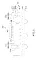
- FIG. 1illustrates a perspective view of semiconductor device package, according to an embodiment of the invention.
- FIG. 2illustrates a cross-sectional view of the package of FIG. 1 , taken along line A-A of FIG. 1 , according to an embodiment of the invention.
- FIG. 3illustrates a cross-sectional view of a stacked device assembly, according to an embodiment of the invention.
- FIG. 4A through FIG. 4Sillustrate a method of forming the semiconductor device package of FIG. 2 , according to an embodiment of the invention.
- a setrefers to a collection of one or more components.
- a set of layerscan include a single layer or multiple layers.
- Components of a setalso can be referred to as members of the set.
- Components of a setcan be the same or different.
- components of a setcan share one or more common characteristics.
- adjacentrefers to being near or adjoining. Adjacent components can be spaced apart from one another or can be in actual or direct contact with one another. In some instances, adjacent components can be connected to one another or can be formed integrally with one another.
- relative termssuch as “inner,” “interior,” “outer,” “exterior,” “top,” “bottom,” “front,” “back,” “upper,” “upwardly,” “lower,” “downwardly,” “vertical,” “vertically,” “lateral,” “laterally,” “above,” and “below,” refer to an orientation of a set of components with respect to one another, such as in accordance with the drawings, but do not require a particular orientation of those components during manufacturing or use.
- connectionrefers to an operational coupling or linking.
- Connected componentscan be directly coupled to one another or can be indirectly coupled to one another, such as through another set of components.
- the terms “substantially” and “substantial”refer to a considerable degree or extent. When used in conjunction with an event or circumstance, the terms can refer to instances in which the event or circumstance occurs precisely as well as instances in which the event or circumstance occurs to a close approximation, such as accounting for typical tolerance levels of the manufacturing operations described herein.
- electrically conductiveand “electrical conductivity” refer to an ability to transport an electric current. Electrically conductive materials typically correspond to those materials that exhibit little or no opposition to flow of an electric current. One measure of electrical conductivity is in terms of Siemens per meter (“S ⁇ m ⁇ 1 ”). Typically, an electrically conductive material is one having a conductivity greater than about 10 4 such as at least about 10 5 S ⁇ m ⁇ 1 or at least about 10 6 S ⁇ m ⁇ 1 . Electrical conductivity of a material can sometimes vary with temperature. Unless otherwise specified, electrical conductivity of a material is defined at room temperature.
- FIG. 1 and FIG. 2illustrate a semiconductor device package 100 implemented in accordance with an embodiment of the invention.
- FIG. 1illustrates a perspective view of the package 100
- FIG. 2illustrates a cross-sectional view of the package 100 , taken along line A-A of FIG. 1 .
- sides of the package 100are substantially planar and have a substantially orthogonal orientation so as to define a lateral profile that extends around substantially an entire periphery of the package 100 .
- this orthogonal lateral profileallows a reduced overall package size by reducing or minimizing a footprint area of the package 100 .
- the lateral profile of the package 100in general, can be any of a number of shapes, such as curved, inclined, stepped, or roughly textured.
- the semiconductor device package 100includes a semiconductor device 202 , which includes a lower surface 204 , an upper surface 206 , and lateral surfaces 208 and 210 disposed adjacent to a periphery of the semiconductor device 202 and extending between the lower surface 204 and the upper surface 206 .
- each of the surfaces 204 , 206 , 208 , and 210is substantially planar, with the lateral surfaces 208 and 210 having a substantially orthogonal orientation with respect to the lower surface 204 or the upper surface 206 , although it is contemplated that the shapes and orientations of the surfaces 204 , 206 , 208 , and 210 can vary for other implementations.
- FIG. 1the semiconductor device package 100 includes a semiconductor device 202 , which includes a lower surface 204 , an upper surface 206 , and lateral surfaces 208 and 210 disposed adjacent to a periphery of the semiconductor device 202 and extending between the lower surface 204 and the upper surface 206 .
- the upper surface 206is a back surface of the semiconductor device 202
- the lower surface 204is an active surface of the semiconductor device 202
- connectors 212 a and 212 bare disposed adjacent to the lower surface 204 . These connectors 212 provide input and output electrical connections for the semiconductor device 202 to conductive structures included in the package 100 , such as a patterned conductive layer 250 (described below).
- the connectors 212may be solder bumps.
- an underfill layer 213may optionally be added between the lower surface 204 and an interconnection unit 240 (described below).
- the underfill layer 213may include epoxy, resin, or other suitable materials.
- the semiconductor device 202is a semiconductor chip, although it is contemplated that the semiconductor device 202 , in general, can be any active device, any passive device, or a combination thereof. While one semiconductor device is illustrated in FIG. 2 , it is contemplated that additional semiconductor devices can be included for other implementations.
- the semiconductor device package 100also includes a package body 214 that is disposed adjacent to the semiconductor device 202 .
- the package body 214substantially covers or encapsulates the semiconductor device 202 in conjunction with the underfill layer 213 and an upper surface 242 of the interconnection unit 240 (described below) to provide mechanical stability as well as protection against oxidation, humidity, and other environmental conditions.
- the package body 214substantially covers the upper surface 206 and the lateral surfaces 208 and 210 of the semiconductor device 202 , with the lower surface 204 the semiconductor device 202 being substantially exposed or uncovered by the package body 214 .
- the extent of coverage by the package body 214can be varied from that illustrated in FIG. 2 .
- the package body 214can substantially cover the lateral surfaces 208 and 210 , while both the lower surface 204 and the upper surface 206 are substantially uncovered.
- the package body 214includes a lower surface 216 , an upper surface 218 , and lateral surfaces 220 and 222 disposed adjacent to a periphery of the package body 214 and extending between the lower surface 216 and the upper surface 218 .
- each of the surfaces 216 , 218 , 220 , and 222is substantially planar, with the lateral surfaces 220 and 222 having a substantially orthogonal orientation with respect to the lower surface 216 and the upper surface 218 , although it is contemplated that the shapes and orientations of the surfaces 216 , 218 , 220 , and 222 can vary for other implementations.
- the package body 214can be formed from a molding material.
- the molding materialcan include, for example, a Novolac-based resin, an epoxy-based resin, a silicone-based resin, or another suitable encapsulant. Suitable fillers can also be included, such as powdered SiO 2 .
- the molding materialmay be a pre-impregnated (prepreg) material, such as a pre-impregnated dielectric material.
- prepregpre-impregnated
- the package body 214can include a supporting structure in conjunction with, or in place of, a molding material.
- the package body 214can include a frame or an interposer, which can be formed from glass, silicon, a metal, a metal alloy, a polymer, or another suitable structural material.
- a layer 230includes a lower surface 232 , an upper surface 234 , and lateral surfaces 236 and 238 disposed adjacent to a periphery of the layer 230 and extending between the lower surface 232 and the upper surface 234 .
- each of the surfaces 234 , 236 , and 238is substantially planar, with the lateral surfaces 236 and 238 having a substantially orthogonal orientation with respect to the upper surface 234 , although it is contemplated that the shapes and orientations of the surfaces 234 , 236 , and 238 can vary for other implementations.
- the lower surface 232is shown as extending into openings in the patterned conductive layer 250 (described below), although it is contemplated that the shape and orientation of the lower surface 232 can vary for other implementations.
- the lower surface 232may be substantially planar.
- the upper surface 234may be adjacent to the lower surface 216 of the package body 214 .
- the layer 230can be formed from a dielectric material that is polymeric or non-polymeric.
- the layer 230can be formed from polyimide, polybenzoxazole, benzocyclobutene, or a combination thereof.
- the layer 230can be formed from a dielectric material that is photoimageable or photoactive.
- the layer 230can be formed from solder mask (solder resist), such as dry film imageable solder mask, or another type of patternable layer or dielectric layer.
- a thickness of the layer 230may be in the range 10 microns to 30 microns, such as a range of 10 microns to 20 microns, or a range of 20 microns to 30 microns. While one layer 230 is illustrated in FIG. 2 as part of the package 100 , it is contemplated that more or less layers of similar composition and characteristics to the layer 230 can be included in a semiconductor device package in other embodiments.
- the semiconductor device package 100further includes the patterned conductive layer 250 adjacent to the lower surface 232 of the layer 230 .
- the patterned conductive layer 250has an upper surface 252 and a lower surface 254 .
- the patterned conductive layer 250may include electrical interconnects 251 a and 251 b.
- the electrical interconnects 251 a and 251 bmay extend substantially laterally within the patterned conductive layer 250 .
- the electrical interconnects 251 a and 251 bhave first surfaces 253 a and 253 b, respectively, that may be included in the upper surface 252 of the patterned conductive layer 250 .
- the package 100further includes electrical interconnects 260 a and 260 b.
- the electrical interconnect 251 amay electrically connect the electrical interconnect 260 a to an electrical contact 294 a or another electrical interconnect (not shown). In one embodiment, the electrical interconnect 251 a may be adjacent to the electrical contact 294 a or the another electrical interconnect at an opening 286 a in a protection layer 284 adjacent to the patterned conductive layer 250 .
- the electrical interconnect 251 bmay electrically connect the electrical interconnect 260 b to an electrical contact 294 b or another electrical interconnect (not shown). In one embodiment, the electrical interconnect 251 b may be adjacent to the electrical contact or the another electrical interconnect at an opening 286 b in the protection layer 284 .
- the electrical interconnects 260 a and 260 bhave lower surfaces 262 a and 262 b, lateral surfaces 264 a and 264 b, and upper surfaces 266 a and 266 b, respectively.
- the electrical interconnects 260 a and 260 bare positioned around the semiconductor device 202 , and may extend substantially vertically from the first surfaces 253 a and 253 b, respectively.
- the lower surfaces 262 a and 262 bmay be adjacent to the first surfaces 253 a and 253 b , respectively.
- At least a portion of the first surfaces 253 a and 253 bmay be substantially covered by the layer 230 .
- At least a portion of the lateral surfaces 264 a and 264 bmay be substantially covered by the package body 214 .
- At least a portion of the lateral surfaces 264 a and 264 bmay be substantially covered by the layer 230 .
- the layer 230may be formed so as to define openings 233 a and 233 b, which are aligned and sized so as to accommodate the connectors 212 a and 212 b, respectively.
- the connectors 212 a and 212 bmay be adjacent to the upper surface 252 of the patterned conductive layer 250 .
- the connectors 212 a and 212 bmay be adjacent to plating layers 256 a and 256 b (or finish layers 256 a and 256 b ), respectively.
- the plating layers 256 a and 256 bmay be disposed adjacent to the upper surface 252 of the patterned conductive layer 250 , and may be disposed in the openings 233 a and 233 b, respectively.
- the patterned conductive layer 250may be included in the interconnection unit 240 .
- the plating layers 256 a and 256 b and the layer 230may optionally be included in the interconnection unit 240 .
- the patterned conductive layer 250may extend substantially laterally within the interconnection unit 240 .
- the upper surface 252 of the patterned conductive layer 250may be included in the upper surface 242 of the interconnection unit 240 .
- the upper surfaces 257 a and 257 b of the plating layers 256 a and 256 b, respectively, and the upper surface 234 of the layer 230may be included in the upper surface 242 of the interconnection unit 240 .
- the interconnection unit 240also includes a lower surface 243 .
- the lower surface 254 of the patterned conductive layer 250may be included in the lower surface 243 .
- portions of the lower surface 232 of the layer 230may be included in the lower surface 243 .
- the package body 214is formed so as to define openings 215 a and 215 b.
- the layer 230is formed so as to define openings 231 a and 231 b , where the openings 231 a and 231 b may be substantially aligned with the openings 215 a and 215 b, respectively.
- the openings 215 a and 215 bmay extend from the upper surface 218 to the upper surfaces 266 a and 266 b of the electrical interconnects 260 a and 260 b, respectively, and may expose the upper surfaces 266 a and 266 b.
- the openings 231 a and 231 bmay extend from the upper surface 234 to the lower surface 232 of the layer 230 , and may be disposed adjacent to the upper surface 252 of the patterned conductive layer 250 .
- the upper surface 266 a of the electrical interconnect 260 amay define a plane 246 a above a plane 247 defined by at least a portion of the upper surface 242 of the interconnection unit 240 (such as at least one of the upper surfaces 257 a and 257 b of the plating layers 256 a and 256 b, respectively), and below a plane 248 defined by the upper surface 218 of the package body 214 .
- the upper surface 266 b of the electrical interconnect 260 bmay define a plane 246 b above the plane 247 , and below the plane 248 .
- the electrical interconnect 260 amay substantially fill the opening 231 a
- the electrical interconnect 260 bmay substantially fill the opening 231 b, such that at least one of the planes 246 a and 246 b is above a plane 244 defined by the upper surface 234 of the layer 230 .
- at least one of the planes 246 a and 246 b, respectively,may be above the plane 247 , and below the plane 248 .
- connecting elements 292 a and 292 bare exposed at an external periphery of the semiconductor device package 100 .
- the connecting elements 292 a and 292 bprovide input and output electrical connections for the package 100 , and at least one of the connecting elements 292 a and 292 b is electrically connected to the semiconductor device 202 through at least one of the electrical interconnects 260 and the patterned conductive layer 250 .
- the connecting elements 292 a and 292 bare conductive bumps, such as solder bumps.
- the connecting elements 292 a and 292 bmay be fused conductive bumps, such as solder bumps that have been reflowed and combined with other conductive elements, such as other solder bumps.
- the fused conductive bumpsmay be formed to provide electrical connectivity between the package 100 and another semiconductor device (shown in FIG. 3 ) and/or semiconductor device package stacked above the package 100 .
- the connecting elements 292 a and 292 bare physically accessible from outside the package 100 . This physical accessibility of the connecting elements 292 , for example, would enable reflowing of the connecting elements 292 as part of stacking of another semiconductor device and/or package on the package 100 .
- the connecting elements 292may be formed from solder paste, where the solder paste may include at least one of tin, copper, and various other suitable metals.
- the openings 215 a and 215 bmay be sized so that the connecting elements 292 a and 292 b may substantially fill the openings 215 a and 215 b , respectively, to minimize and/or prevent voids.
- the prevention of voids within the openings 215 a and 215 bis desirable to enhance the electrical connectivity characteristics of the electrical interconnects 260 and the connecting elements 292 , and therefore between the package 100 and another semiconductor device (shown in FIG. 3 ) and/or semiconductor device package stacked above the package 100 .
- a further advantage of controlling the sizing of the openings 215 a and 215 bis to facilitate control of the volume of conductive material forming the connecting elements 292 a and 292 b.
- voidscan be minimized and/or prevented within the openings 215 a and 215 b by sizing the electrical interconnects 260 a and 260 b so that the planes 246 a and 246 b are above the plane 247 , and therefore so that heights 270 a and 270 b of the openings 215 a and 215 b are controlled. In one embodiment, it may be desirable for heights 270 a and 270 b of the openings 215 a and 215 b , respectively, to be 400 microns or less to minimize and/or prevent voids within the openings 215 a and 215 b.
- a height 272 of the package body 214may be in the range 200 microns to 500 microns, such as a range of 200 microns to 300 microns, a range of 300 microns to 400 microns, or a range of 400 microns to 500 microns.
- heights 274 a and 274 b of the electrical interconnects 260 a and 260 b, respectivelymay be sufficiently large (such as greater than 100 microns) so that the heights 270 a and 270 b of the openings 215 a and 215 b are 400 microns or less.
- the heights 270 a and 270 bmay be greater, the same, or smaller than the heights 274 a and 274 b.
- the connecting elements 292 a and 292 bmay protrude beyond the upper surface 218 of the package body 214 .
- This protrusion of the connecting elements 292 a and 292 bmay increase the contact area of the connecting elements 292 a and 292 b that is exposed, which may enable a stronger physical join and better electrical connectivity between the package 100 and another semiconductor device (shown in FIG. 3 ) and/or semiconductor device package stacked above the package 100 .
- the connecting elements 292 a and 292 bmay not extend beyond the upper surface 218 of the package body 214 .
- the connecting elements 292 a and 292 bmay extend to, but not beyond, the upper surface 218 such that the openings 215 a and 215 b are substantially filled.
- portions 224 a and 224 b of the openings 215 a and 215 bare adjacent to the upper surfaces 266 a and 266 b of the electrical interconnects 260 a and 260 b, respectively.
- Width 226 a of the portion 224 amay be less than width 275 a of the upper surface 266 a
- width 226 b of the portion 224 bmay be less than width 275 b of the upper surface 266 b.
- portions 223 a and 223 b of the openings 215 a and 215 bare adjacent to the plane 248 defined by the upper surface 218 of the package body 214 .
- Width 225 a of the portion 223 amay be greater than the width 226 a of the portion 224 a, and width 225 b of the portion 223 b may be greater than the width 226 b of the portion 224 b.
- the patterned conductive layer 250may serve as a redistribution network for the semiconductor device 202 .
- the semiconductor device package 100may provide a fan-out configuration in which the patterned conductive layer 250 extends substantially laterally outside of the periphery of the semiconductor device 202 .
- FIG. 2shows the electrical interconnects 251 a and 251 b outside of the periphery of the semiconductor device 202 .
- the electrical interconnects 251 a and 251 bmay be electrically connected to the semiconductor device 202 via other electrical interconnects in the patterned conductive layer 250 (not shown).
- the fan-out configuration of the package 100allows greater flexibility in terms of the arrangement and spacing of the electrical contacts 294 a and 294 b, with reduced dependence upon the arrangement and spacing of contact pads the semiconductor device 202 .
- the electrical interconnects 260 a and 260 b and the connecting elements 292 a and 292 bcan facilitate extending this to a three-dimensional fan-out (see FIG. 3 ) by providing electrical pathways from the semiconductor device 202 to the upper surface of the package 100 .
- the electrical contacts 294 a and 294 bprovide input and output electrical connections for the package 100 , and at least one of the electrical contacts 294 a and 294 b is electrically connected to the semiconductor device 202 through the electrically conductive layer 250 .
- the electrical contacts 294 a and 294 bare conductive bumps, such as solder bumps.
- the electrical contacts 294 a and 294 bmay be fused conductive bumps, such as solder bumps that have been reflowed and combined with other conductive elements, such as other solder bumps.
- the connecting elements 292 a and 292 b and the electrical contacts 294 a and 294 bare laterally disposed outside of the periphery of the semiconductor device 202 , although it is contemplated that the electrical contacts 294 a and 294 b, in general, can be laterally disposed within that periphery, outside of that periphery, or both.
- the fan-out configuration of the package 100allows greater flexibility in terms of the arrangement and spacing of the electrical contacts 294 a and 294 b, with reduced dependence upon the arrangement and spacing of the contact pads of the semiconductor device 202 .
- the patterned conductive layer 250 and each of the electrical interconnects 260 a and 260 bcan be formed from a metal, a metal alloy, a matrix with a metal or a metal alloy dispersed therein, or another suitable electrically conductive material.
- at least one of the patterned conductive layer 250 and the electrical interconnects 260 a and 260 bcan be formed from aluminum, copper, titanium, or a combination thereof.
- the patterned conductive layer 250 and the electrical interconnects 260 a and 260 bcan be formed from the same electrically conductive material or different electrically conductive materials.
- the plating layers 256 a and 256 bcan be formed similarly to the patterned conductive layer 250 , as described previously. Alternatively, the plating layers 256 a and 256 b may be formed differently. For example, the plating layers 256 a and 256 b may be formed from at least one of tin, nickel, and gold, or an alloy including tin or including nickel and gold. The plating layers 256 a and 256 b can be formed from the same electrically conductive material or different electrically conductive materials.
- the protection layer 284can be formed similarly to the layer 230 , as described previously.
- the protection layer 284may be formed using solder mask (solder resist), such as dry film imageable solder mask, or another type of patternable layer or dielectric layer. While one protection layer 284 is illustrated in FIG. 2 , it is contemplated that more or less protection layers can be included for other implementations. Openings in the protection layer 284 , such as the openings 286 a and 286 b, may expose portions of the electrically conductive layer 250 , such as portions of at least one of the electrical interconnects 251 a and 251 b .
- the openings 286 a and 286 bmay be substantially aligned with at least one of the lower surfaces 262 a and 262 b of the electrical interconnects 260 a and 260 b, respectively.
- the protection layer 284may be patterned to form the openings 286 .
- the openings 286can have any of a number of shapes, including a cylindrical shape, such as a circular cylindrical shape, an elliptic cylindrical shape, a square cylindrical shape, or a rectangular cylindrical shape, or a non-cylindrical shape, such as a cone, a funnel, or another tapered shape. It is also contemplated that lateral boundaries of the resulting openings can be curved or roughly textured.
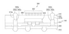
- FIG. 3illustrates a cross-sectional view of a stacked device assembly 300 , according to an embodiment of the invention.
- the stacked device assembly 300includes a semiconductor device 302 stacked on the package 100 .
- the semiconductor device 302may be unpackaged.
- the stacked device assemblymay include another semiconductor device package (not shown) stacked on the package 100 .
- the another semiconductor device packagemay be similar to the package 100 , may include a patterned conductive layer similar to the patterned conductive layer 250 , and may include a semiconductor device similar to the semiconductor device 202 .
- the semiconductor device 302 and/or the another semiconductor device packagemay be disposed adjacent to or above the upper surface 218 of the package body 214 . While the stacked device assembly 300 is illustrated in FIG. 3 as including a two-layer stack, it is contemplated that the stack may include more than two layers for other implementations.
- the stacked device assembly 300may include stacking elements 304 a and 304 b, at least one of which electrically connects the semiconductor device 202 and the semiconductor device 302 through the patterned conductive layer 250 and a patterned conductive layer 306 .
- the stacking element 304 aincludes the electrical interconnect 260 a and the connecting element 292 a
- the stacking element 304 bincludes the electrical interconnect 260 b and the connecting element 292 b.
- the stacking element 304 amay extend through and substantially fill the opening 215 a in the package body 214
- the stacking element 304 bmay extend through and substantially fill the opening 215 b in the package body 214 .
- the connecting elements 292 a and 292 bare in the form of fused conductive bumps exposed at an external periphery of the stacked device assembly 300 . As described previously, the connecting elements 292 may be physically accessible from outside the package 100 .
- the connecting elements 292 a and 292 bmay be fused to the patterned conductive layer 306 to form fused conductive bumps exposed at an external periphery of the stacked device assembly 300 .
- the patterned conductive layer 306may be disposed adjacent to the upper surface of the package body 214 .
- the connecting elements 292 a and 292 bmay be fused to electrical contacts (similar to electrical contacts 294 a and 294 b ) of the another semiconductor package stacked on the package 100 , where the electrical contacts are electrically connected to a patterned conductive layer (similar to the patterned conductive layer 250 ) in the another semiconductor device package.
- the stacked device assembly 300may include the patterned conductive layer 306 , which may serve as a redistribution network for the semiconductor device 302 .
- the stacked device assembly 300may provide a fan-out configuration in which the patterned conductive layer 306 is electrically connected to the semiconductor device 302 and extends substantially laterally outside of the periphery of the semiconductor device 302 .
- the electrical interconnects 260 a and 260 b and the connecting elements 292 a and 292 b of the package 100can facilitate extending a two-dimensional fan-out to a three-dimensional fan-out by providing electrical pathways from the semiconductor device 202 to the upper surface of the package 100 .
- a three-dimensional fan-out configurationcan be created by electrically connecting the connecting elements 292 a and 292 b to the patterned conductive layer 306 .
- This three-dimensional fan-out configurationcan advantageously increase flexibility beyond that provided by two-dimensional fan-out in terms of the arrangement and spacing of electrical contacts on both an upper side 310 and a lower side 312 of the stacked device assembly 300 .
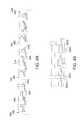
- FIG. 4A through FIG. 4Sillustrate a method of forming the semiconductor device package 100 of FIG. 2 , according to an embodiment of the invention.
- the following manufacturing operationsare described with reference to the package 100 of FIG. 2 .
- the manufacturing operationscan be similarly carried out to form other semiconductor device packages that may have different internal structure from the package 100 .
- a carrier 400is provided, and an electrically conductive layer 402 is disposed adjacent to an upper surface 401 of the carrier 400 .
- the electrically conductive layer 402has an upper surface 404 , and may include multiple sub-layers 402 a and 402 b.
- the sub-layer 402 amay be formed from a metal, a metal alloy, a matrix with a metal or a metal alloy dispersed therein, or another suitable electrically conductive material.
- the sub-layer 402 amay include a metallic foil formed from copper or an alloy including copper.
- the sub-layer 402 amay be attached to the carrier 400 with a tape (not shown) disposed adjacent to the upper surface 401 of the carrier 400 .
- the tapewhich can be implemented as a single-sided or double-sided adhesive tape, secures components at an appropriate spacing with respect to one another, and allows subsequent manufacturing operations to be carried out with those components disposed adjacent to the carrier 400 .
- the sub-layer 402 bmay be applied to an upper surface 403 of the sub-layer 402 a.
- the sub-layer 402 bmay be applied using any of a number of coating techniques, such as chemical vapor deposition, electroless plating, electrolytic plating, printing, spinning, spraying, sputtering, or vacuum deposition.
- the sub-layer 402 bmay be formed from a metal, a metal alloy, a matrix with a metal or a metal alloy dispersed therein, or another suitable electrically conductive material.
- the sub-layer 402 bmay be formed of an electrically conductive material different from that used to form the sub-layer 402 a.
- the sub-layer 402 bmay serve as an etch stop layer, and may include nickel or an alloy including nickel.
- a photoresist materialmay be applied to the upper surface 404 of the electrically conductive layer 402 to form a photoresist layer 406 adjacent to the upper surface 404 .
- the photoresist materialmay be a dry film photoresist, or another type of patternable layer or dielectric layer.
- the photoresist layer 406may be formed by coating, printing, or any other suitable technique. Predetermined or selected portions of the photoresist layer 406 may be photoimaged and developed so as to create openings, including openings 408 a - 408 e, exposing the upper surface 404 of the electrically conductive layer 402 .
- the photoresist layer 406may be photochemically defined using a photomask (not shown).
- Photoimaging and developingmay have advantages of lower cost and decreased process time as compared to other approaches for creating openings in the photoresist layer 406 .
- the resulting openingscan have any of a number of shapes, including a cylindrical shape, such as a circular cylindrical shape, an elliptic cylindrical shape, a square cylindrical shape, or a rectangular cylindrical shape, or a non-cylindrical shape, such as a cone, a funnel, or another tapered shape. It is also contemplated that lateral boundaries of the resulting openings can be curved or roughly textured.
- an electrically conductive materialis applied into the openings, including openings 408 a - 408 e, defined by the photoresist layer 406 to form an electrically conductive layer 450 , including electrical interconnects 451 a and 451 b.
- the electrically conductive layer 450 and the electrical interconnects 451 a and 451 bmay extend substantially laterally, and may be formed using the same types of materials as previously described for the electrically conductive layer 250 and the electrical interconnects 251 a and 251 b (shown in FIG. 2 ).
- the patterned conductive layer 450may be formed using any of a number of coating techniques, such as chemical vapor deposition, electroless plating, electrolytic plating, printing, spinning, spraying, sputtering, or vacuum deposition.
- the photoresist layer 406is stripped to expose portions of the sub-layer 402 b.
- a layer 430is formed adjacent to the patterned conductive layer 450 and the exposed portions of the sub-layer 402 b.
- the layer 430may substantially cover an upper surface 452 of the patterned conductive layer 450 , such that the patterned conductive layer 450 is embedded in the layer 430 .
- a dielectric materialmay be applied using any of a number of coating techniques, such as printing, spinning, or spraying.
- the layer 430may be created by laminating a dielectric material on the upper surface 452 of the patterned conductive layer 450 (including first surfaces 453 a and 453 b, corresponding to first surfaces 253 a and 253 b in FIG.
- the layer 430may be created by spreading the dielectric material in liquid form on the upper surface 452 of the patterned conductive layer 450 (including the first surfaces 453 a and 453 b ) and the exposed portions of the sub-layer 402 b.
- the layer 430can be formed from solder mask (solder resist), such as dry film imageable solder mask, or another type of patternable layer or dielectric layer.
- solder masksolder resist
- the layer 430may be formed using the same types of materials as previously described for the layer 230 (shown in FIG. 2 ).
- the openings 231 a and 231 bare formed in the layer 430 to expose the first surfaces 453 a and 453 b of the electrical interconnects 451 a and 451 b, respectively.
- the openings 233 a and 233 bare formed in the layer 430 to expose additional portions of the upper surface 452 of the patterned conductive layer 450 .
- the layer 430is patterned to form the openings 231 a, 231 b, 233 a, and 233 b.
- the openings 231 a, 231 b, 233 a, and 233 bmay extend from an upper surface 434 of the layer 430 to a lower surface 432 of the layer 430 .
- Patterning to form the layer 430can be carried out in any of a number of ways, such as photolithography, chemical etching, laser drilling, or mechanical drilling, and the resulting openings can have any of a number of shapes, such as a cylindrical shape, such as a circular cylindrical shape, an elliptic cylindrical shape, a square cylindrical shape, or a rectangular cylindrical shape, or a non-cylindrical shape, such as a cone, a funnel, or another tapered shape. It is also contemplated that lateral boundaries of the resulting openings can be curved or roughly textured.
- a photoresist materialmay be applied to the upper surface 434 of the layer 430 to form a photoresist layer 410 adjacent to the upper surface 434 .
- the photoresist materialmay be a dry film photoresist, or another type of patternable layer or dielectric layer.
- the photoresist layer 410may be formed as described previously for FIG. 4B . Also as described previously for FIG. 4B , predetermined or selected portions of the photoresist layer 410 may be photoimaged and developed so as to create openings, including openings 412 a and 412 b.
- the openings 412 a and 412 bmay be aligned with the openings 233 a and 233 b, respectively, to expose portions of the upper surface 452 of the patterned conductive layer 450 .
- the openings 412 a and 412 bmay have characteristics similar to those of the openings 408 a - 408 e.
- an electrically conductive materialis applied into the openings 233 a and 233 b that expose portions of the upper surface 452 of the patterned conductive layer 450 .
- the plating layers 256 a and 256 bmay be formed using any of the techniques described previously for FIG. 4C .
- the photoresist layer 410is stripped to expose the upper surface 434 of the layer 430 , and the first surfaces 453 a and 453 b of the electrical interconnects 451 a and 451 b, respectively.
- the stripping of the photoresist layer 410exposes the interconnection structure 440 , which by this point has been formed.
- the interconnection structure 440includes the layer 430 , the patterned conductive layer 450 , and the plating layers 256 a and 256 b.
- the interconnection structure 440may include the patterned conductive layer 450 , and may optionally include the plating layers 256 a and 256 b without including the layer 430 .
- the upper surface 452 of the patterned conductive layer 450may be included in an upper surface 442 of the interconnection structure 440 .
- the upper surfaces 257 a and 257 b of the plating layers 256 a and 256 b, respectively, and the upper surface 434 of the layer 430may be included in the upper surface 442 of the interconnection structure 440 .
- the lower surface 454 of the patterned conductive layer 450may be included in the lower surface 443 of the interconnection structure 440 .
- portions of a lower surface 432 of the layer 430may be included in the lower surface 443 .
- a photoresist materialmay be applied to the upper surface 434 of the layer 430 and to the plating layers 256 a and 256 b to form a photoresist layer 414 adjacent to the upper surface 434 and to the plating layers 256 a and 256 b.
- the photoresist materialmay be a dry film photoresist, or another type of patternable layer or dielectric layer.
- the photoresist layer 414may be formed as described previously for FIG. 4B . Also as described previously for FIG. 4B , predetermined or selected portions of the photoresist layer 414 may be photoimaged and developed so as to create openings, including openings 416 a and 416 b.
- the openings 416 a and 416 bmay be aligned with the openings 231 a and 231 b, respectively, to expose the first surfaces 453 a and 453 b.
- the openings 416 a and 416 bmay have characteristics similar to those of the openings 408 a - 408 e.
- an electrically conductive materialis applied into the openings 416 a and 416 b defined by the photoresist layer 414 , and into the openings 231 a and 231 b, to form electrical interconnects 260 a and 260 b, respectively.
- the electrical interconnects 260 a and 260 bmay be formed extending substantially vertically away from the electrically conductive layer 402 .
- the electrical interconnect 260 amay substantially fill the openings 416 a and 231 a, and the electrical interconnect 260 b may substantially fill the openings 416 b and 231 b.
- the planes 246 a and 246 b defined by the upper surfaces 266 a and 266 b of the electrical interconnects 260 a and 260 bmay be below a plane 417 defined by an upper surface 415 of the photoresist layer 414 .
- the electrical interconnects 260 a and 260 bmay be formed using any of a number of coating techniques, such as electrolytic plating or plugging a paste composed of the electrically conductive material.
- the photoresist layer 414is stripped to expose the upper surface 434 of the layer 430 , the plating layers 256 a and 256 b, and the lateral surfaces 264 a and 264 b of the electrical interconnects 260 a and 260 b, respectively.
- both the interconnection structure 440 and the electrical interconnects 260 a and 260 bhave been formed.
- the interconnection structure 440 and the electrical interconnects 260 a and 260 bcan be tested. As a result, the semiconductor device 202 will be attached (such as illustrated in FIG.
- the semiconductor device 202is disposed adjacent to the upper surface 442 of the interconnection structure 440 .
- the semiconductor device 202may be flip-chip bonded such that the semiconductor device 202 is electrically connected to the patterned conductive layer 450 and the electrical interconnects 260 a and 260 b via the connectors 212 a and 212 b.
- the underfill layer 213may optionally be added between the lower surface 204 of the semiconductor device 202 and the layer 430 .
- a molding materialmay be applied to form a molded structure 480 .
- the molded structure 480may substantially cover or encapsulate the top surface 206 and the lateral surfaces 208 and 210 of the semiconductor device 202 .
- the molded structuremay also substantially cover or encapsulate the lateral surfaces 264 a and 264 b and the upper surfaces 266 a and 266 b of the electrical interconnects 260 a and 260 b , respectively.
- the molding material that forms the molded structure 480can include, for example, a Novolac-based resin, an epoxy-based resin, a silicone-based resin, or another suitable encapsulant. Suitable fillers also can be included, such as powdered SiO 2 .
- the molded structure 480can be formed using any of a number of molding techniques, such as injection molding. Once applied, the molding material is hardened or solidified, such as by lowering the temperature to below a melting point of the molding material, thereby forming the molded structure 480 . To facilitate proper positioning of the molded structure 480 during subsequent singulation operations, fiducial marks can be formed in the molded structure 480 , such as using laser marking.
- the openings 215 a and 215 bmay be formed in the molded structure 480 .
- the openings 215 a and 215 bmay be adjacent to an upper surface 482 of the molded structure 480 , and may expose the upper surfaces 266 a and 266 b of the electrical interconnects 260 a and 260 b, respectively.
- the distance 274 ais from the upper surface 266 a to the lower surface 262 a of the electrical interconnect 260 a
- the distance 274 bis from the upper surface 266 b to the lower surface 262 b of the electrical interconnect 260 b.
- the distance 434is from the plane 247 defined by the upper surface 442 of the interconnection structure 440 to the lower surface 443 of the interconnection structure 440 .
- the plane 247is defined based on at least one of the upper surfaces 257 a and 257 b of the plating layers 256 a and 256 b, respectively.
- the distance 434may be from a different portion of the upper surface 442 to the lower surface 443 .
- the distance 434may be from the upper surface 434 of the layer 430 to the lower surface 443 . At least one of the distances 274 a and 274 b may be greater than the distance 434 .
- the openings 215 a and 215 bmay be formed by drilling to remove a portion of the molded structure 480 adjacent to the upper surface 482 of the molded structure 480 . It may be advantageous to use laser drilling, rather than mechanical drilling, to minimize the potential for damage to structures encapsulated by the molded structure 480 (such as the electrical interconnects 260 , the interconnection structure 440 , and the semiconductor device 202 ) due to the drilling.
- the connecting elements 292 a and 292 bare formed.
- the connecting elements 292 a and 292 bmay substantially fill the openings 215 a and 215 b, respectively.
- the connecting elements 292may protrude beyond a plane 483 defined by the upper surface 482 of the molded structure 480 .
- the connecting elements 292 a and 292 bmay be electrically connected to the electrical interconnects 260 a and 260 b, respectively.
- the connecting elements 292 a and 292 bmay be formed from solder paste, where the solder paste may include at least one of tin, copper, and various other suitable metals.
- the connecting elements 292 a and 292 bmay be formed through printing, plugging, plating, or through other suitable techniques.
- the connecting elements 292 a and 292 bare formed in openings 215 a and 215 b drilled into the molded structure 480 .
- the carrier 400is removed, exposing the electrically conductive layer 450 .
- a protection layer 484is then formed adjacent to the electrically conductive layer 450 .
- the protection layer 484can be formed similarly to the protection layer 284 , as described previously. While one protection layer 484 is illustrated in FIG. 4M , it is contemplated that more or less protection layers can be included for other implementations. Openings in the protection layer 484 , such as the openings 286 a and 286 b , may expose portions of the electrically conductive layer 450 .
- the protection layer 484may be patterned to form the openings 286 a and 286 b, similarly to the patterning of the layer 430 described previously.
- Singulationis next carried out along the dashed lines 490 , as illustrated in FIG. 4R .
- singulationmay be carried out using a saw (not shown), which forms cutting slits 492 .
- the alignment of the saw during singulationcan be aided by fiducial marks, which allow proper positioning of the saw when forming the cutting slits 492 .
- the cutting slits 492extend completely through the molded structure 480 , the interconnection structure 440 , and the protection layer 484 , thereby sub-dividing the molded structure 480 , the interconnection structure 440 , and the protection layer 484 into discrete units, including the package body 214 , the interconnection unit 240 , and the protection layer 284 .
- external connectorssuch as solder bumps may be electrically connected to the interconnection unit 240 , such as electrical contacts 294 a and 294 b in the openings 286 a and 286 b, respectively.
Landscapes
- Engineering & Computer Science (AREA)
- Microelectronics & Electronic Packaging (AREA)
- Power Engineering (AREA)
- Computer Hardware Design (AREA)
- Physics & Mathematics (AREA)
- Condensed Matter Physics & Semiconductors (AREA)
- General Physics & Mathematics (AREA)
- Manufacturing & Machinery (AREA)
- Internal Circuitry In Semiconductor Integrated Circuit Devices (AREA)
- Wire Bonding (AREA)
Abstract
Description
- The invention relates generally to semiconductor device packages and manufacturing methods thereof. More particularly, the invention relates to semiconductor device packages with metal pillars and via holes and manufacturing methods thereof.
- Electronic products have become progressively more complex, driven at least in part by the demand for enhanced functionality and smaller sizes. While the benefits of enhanced functionality and smaller sizes are apparent, achieving these benefits also can create problems. In particular, electronic products typically have to accommodate a high density of semiconductor devices in a limited space. For example, the space available for processors, memory devices, and other active or passive devices can be rather limited in cell phones, personal digital assistants, laptop computers, and other portable consumer products. In conjunction, semiconductor devices are typically packaged in a fashion to provide protection against environmental conditions as well as to provide input and output electrical connections. Packaging of semiconductor devices within semiconductor device packages can take up additional valuable space within electronic products. As such, there is a strong drive towards reducing footprint areas taken up by semiconductor device packages. One approach along this regard is to stack semiconductor device packages on top of one another to form a stacked package assembly. Unfortunately, conventional wafer-level packaging can be inadequate in terms of stacking functionality.
- In addition, in conventional wafer-level packaging, semiconductor devices within a wafer are packaged prior to singulation of the wafer. As such, conventional wafer-level packaging can be restricted to a fan-in configuration, namely electrical contacts and other components of a resulting semiconductor device package are restricted to an area defined by a periphery of a semiconductor device. Any component disposed outside of the periphery of the semiconductor device typically is not supported and typically is removed upon singulation. The restriction of a fan-in configuration presents challenges as device sizes continue to shrink.
- It is against this background that a need arose to develop the semiconductor device package and related methods described herein.
- One aspect of the invention relates to a semiconductor device package. In one embodiment, the semiconductor device package includes: (1) an interconnection unit including an upper surface and a first patterned conductive layer extending substantially laterally within the interconnection unit; (2) an electrical interconnect extending substantially vertically from the first patterned conductive layer, and including: (a) an upper surface; and (b) a lower surface adjacent to an upper surface of the first patterned conductive layer; (3) a first semiconductor device disposed adjacent to the upper surface of the interconnection unit and electrically connected to the first patterned conductive layer; (4) a package body disposed substantially covering the upper surface of the interconnection unit and the first semiconductor device, the package body defining a first opening disposed adjacent to an upper surface of the package body and exposing the upper surface of the electrical interconnect; and (5) a connecting element electrically connected to the first semiconductor device and substantially filling the first opening, the connecting element being exposed at an external periphery of the semiconductor device package. The upper surface of the electrical interconnect defines a first plane above a second plane defined by at least a portion of the upper surface of the interconnection unit, and below a third plane defined by the upper surface of the package body.
- Another aspect of the invention relates to a stacked device assembly. In one embodiment, the stacked device assembly includes: (1) a semiconductor device package including: (a) an interconnection unit including an upper surface; (b) a first semiconductor device disposed adjacent to the upper surface of the interconnection unit and electrically connected to the interconnection unit; and (c) a package body disposed adjacent to the upper surface of the interconnection unit and substantially covering the first semiconductor device, the package body including an upper surface and defining an opening disposed adjacent to the upper surface of the package body; (2) a second semiconductor device disposed adjacent to the upper surface of the package body; and (3) a stacking element extending through the opening in the package body and electrically connecting the first semiconductor device and the second semiconductor device, the stacking element including: (a) an electrical interconnect including an upper surface and extending substantially vertically from the interconnection unit; and (b) a fused conductive bump electrically connected to the first semiconductor device via at least the electrical interconnect and substantially filling the opening, the fused conductive bump being exposed at an external periphery of the stacked device assembly. The upper surface of the electrical interconnect defines a first plane above a second plane defined by at least a portion of the upper surface of the interconnection unit, and below a third plane defined by the upper surface of the package body.
- Another aspect of the invention relates to a method of forming a semiconductor device package. The method of forming a semiconductor device package includes: (1) providing a first semiconductor device; (2) forming an interconnection structure including: (a) an upper surface; (b) a lower surface; and (c) a patterned conductive layer extending substantially laterally within the interconnection structure; (3) forming an electrical interconnect including an upper surface and a lower surface adjacent to an upper surface of the patterned conductive layer, where the electrical interconnect extends substantially vertically from the patterned conductive layer; (4) disposing the first semiconductor device adjacent to the upper surface of the interconnection structure such that the first semiconductor device is electrically connected to the patterned conductive layer; (5) applying a molding material to form a molded structure substantially covering the upper surface of the electrical interconnect and the first semiconductor device; (6) forming a first opening in the molded structure, the first opening being adjacent to an upper surface of the molded structure and exposing the upper surface of the electrical interconnect, where a first distance from the upper surface of the electrical interconnect to the lower surface of the electrical interconnect is greater than a second distance from the upper surface of the interconnection structure to the lower surface of the interconnection structure; and (7) forming a first connecting element electrically connected to the electrical interconnect and substantially filling the first opening.
- Other aspects and embodiments of the invention are also contemplated. The foregoing summary and the following detailed description are not meant to restrict the invention to any particular embodiment but are merely meant to describe some embodiments of the invention.
- For a better understanding of the nature and objects of some embodiments of the invention, reference should be made to the following detailed description taken in conjunction with the accompanying drawings. In the drawings, like reference numbers denote like elements, unless the context clearly dictates otherwise.
FIG. 1 illustrates a perspective view of semiconductor device package, according to an embodiment of the invention.FIG. 2 illustrates a cross-sectional view of the package ofFIG. 1 , taken along line A-A ofFIG. 1 , according to an embodiment of the invention.FIG. 3 illustrates a cross-sectional view of a stacked device assembly, according to an embodiment of the invention.FIG. 4A throughFIG. 4S illustrate a method of forming the semiconductor device package ofFIG. 2 , according to an embodiment of the invention.- The following definitions apply to some of the aspects described with respect to some embodiments of the invention. These definitions may likewise be expanded upon herein.
- As used herein, the singular terms “a,” “an,” and “the” include plural referents unless the context clearly dictates otherwise. Thus, for example, reference to an electrical interconnect can include multiple electrical interconnects unless the context clearly dictates otherwise.
- As used herein, the term “set” refers to a collection of one or more components. Thus, for example, a set of layers can include a single layer or multiple layers. Components of a set also can be referred to as members of the set. Components of a set can be the same or different. In some instances, components of a set can share one or more common characteristics.
- As used herein, the term “adjacent” refers to being near or adjoining. Adjacent components can be spaced apart from one another or can be in actual or direct contact with one another. In some instances, adjacent components can be connected to one another or can be formed integrally with one another.
- As used herein, relative terms, such as “inner,” “interior,” “outer,” “exterior,” “top,” “bottom,” “front,” “back,” “upper,” “upwardly,” “lower,” “downwardly,” “vertical,” “vertically,” “lateral,” “laterally,” “above,” and “below,” refer to an orientation of a set of components with respect to one another, such as in accordance with the drawings, but do not require a particular orientation of those components during manufacturing or use.
- As used herein, the terms “connect,” “connected,” and “connection” refer to an operational coupling or linking. Connected components can be directly coupled to one another or can be indirectly coupled to one another, such as through another set of components.
- As used herein, the terms “substantially” and “substantial” refer to a considerable degree or extent. When used in conjunction with an event or circumstance, the terms can refer to instances in which the event or circumstance occurs precisely as well as instances in which the event or circumstance occurs to a close approximation, such as accounting for typical tolerance levels of the manufacturing operations described herein.
- As used herein, the terms “electrically conductive” and “electrical conductivity” refer to an ability to transport an electric current. Electrically conductive materials typically correspond to those materials that exhibit little or no opposition to flow of an electric current. One measure of electrical conductivity is in terms of Siemens per meter (“S·m−1”). Typically, an electrically conductive material is one having a conductivity greater than about 104such as at least about 105S·m−1or at least about 106S·m−1. Electrical conductivity of a material can sometimes vary with temperature. Unless otherwise specified, electrical conductivity of a material is defined at room temperature.
- Attention first turns to
FIG. 1 andFIG. 2 , which illustrate asemiconductor device package 100 implemented in accordance with an embodiment of the invention. In particular,FIG. 1 illustrates a perspective view of thepackage 100, whileFIG. 2 illustrates a cross-sectional view of thepackage 100, taken along line A-A ofFIG. 1 . - In the illustrated embodiment, sides of the
package 100 are substantially planar and have a substantially orthogonal orientation so as to define a lateral profile that extends around substantially an entire periphery of thepackage 100. Advantageously, this orthogonal lateral profile allows a reduced overall package size by reducing or minimizing a footprint area of thepackage 100. However, it is contemplated that the lateral profile of thepackage 100, in general, can be any of a number of shapes, such as curved, inclined, stepped, or roughly textured. - Referring to
FIG. 2 , thesemiconductor device package 100 includes asemiconductor device 202, which includes alower surface 204, anupper surface 206, andlateral surfaces semiconductor device 202 and extending between thelower surface 204 and theupper surface 206. In the illustrated embodiment, each of thesurfaces lateral surfaces lower surface 204 or theupper surface 206, although it is contemplated that the shapes and orientations of thesurfaces FIG. 2 , theupper surface 206 is a back surface of thesemiconductor device 202, while thelower surface 204 is an active surface of thesemiconductor device 202. In one embodiment,connectors lower surface 204. These connectors212 provide input and output electrical connections for thesemiconductor device 202 to conductive structures included in thepackage 100, such as a patterned conductive layer250 (described below). In one embodiment, the connectors212 may be solder bumps. In one embodiment, anunderfill layer 213 may optionally be added between thelower surface 204 and an interconnection unit240 (described below). Theunderfill layer 213 may include epoxy, resin, or other suitable materials. In the illustrated embodiment, thesemiconductor device 202 is a semiconductor chip, although it is contemplated that thesemiconductor device 202, in general, can be any active device, any passive device, or a combination thereof. While one semiconductor device is illustrated inFIG. 2 , it is contemplated that additional semiconductor devices can be included for other implementations. - As illustrated in
FIG. 2 , thesemiconductor device package 100 also includes apackage body 214 that is disposed adjacent to thesemiconductor device 202. In the illustrated embodiment, thepackage body 214 substantially covers or encapsulates thesemiconductor device 202 in conjunction with theunderfill layer 213 and anupper surface 242 of the interconnection unit240 (described below) to provide mechanical stability as well as protection against oxidation, humidity, and other environmental conditions. In this embodiment, thepackage body 214 substantially covers theupper surface 206 and thelateral surfaces semiconductor device 202, with thelower surface 204 thesemiconductor device 202 being substantially exposed or uncovered by thepackage body 214. However, it is contemplated that the extent of coverage by thepackage body 214 can be varied from that illustrated inFIG. 2 . For example, it is contemplated that thepackage body 214 can substantially cover the lateral surfaces208 and210, while both thelower surface 204 and theupper surface 206 are substantially uncovered. - As illustrated in
FIG. 2 , thepackage body 214 includes alower surface 216, anupper surface 218, andlateral surfaces package body 214 and extending between thelower surface 216 and theupper surface 218. In the illustrated embodiment, each of thesurfaces lateral surfaces lower surface 216 and theupper surface 218, although it is contemplated that the shapes and orientations of thesurfaces - In one embodiment, the
package body 214 can be formed from a molding material. The molding material can include, for example, a Novolac-based resin, an epoxy-based resin, a silicone-based resin, or another suitable encapsulant. Suitable fillers can also be included, such as powdered SiO2. The molding material may be a pre-impregnated (prepreg) material, such as a pre-impregnated dielectric material. It is also contemplated that thepackage body 214 can include a supporting structure in conjunction with, or in place of, a molding material. For example, thepackage body 214 can include a frame or an interposer, which can be formed from glass, silicon, a metal, a metal alloy, a polymer, or another suitable structural material. - As illustrated in
FIG. 2 , alayer 230 includes alower surface 232, anupper surface 234, andlateral surfaces layer 230 and extending between thelower surface 232 and theupper surface 234. In the illustrated embodiment, each of thesurfaces lateral surfaces upper surface 234, although it is contemplated that the shapes and orientations of thesurfaces lower surface 232 is shown as extending into openings in the patterned conductive layer250 (described below), although it is contemplated that the shape and orientation of thelower surface 232 can vary for other implementations. For example, thelower surface 232 may be substantially planar. Theupper surface 234 may be adjacent to thelower surface 216 of thepackage body 214. - In one embodiment, the
layer 230 can be formed from a dielectric material that is polymeric or non-polymeric. For example, thelayer 230 can be formed from polyimide, polybenzoxazole, benzocyclobutene, or a combination thereof. For certain implementations, thelayer 230 can be formed from a dielectric material that is photoimageable or photoactive. In another embodiment, thelayer 230 can be formed from solder mask (solder resist), such as dry film imageable solder mask, or another type of patternable layer or dielectric layer. In one embodiment, a thickness of thelayer 230 may be in the range 10 microns to 30 microns, such as a range of 10 microns to 20 microns, or a range of 20 microns to 30 microns. While onelayer 230 is illustrated inFIG. 2 as part of thepackage 100, it is contemplated that more or less layers of similar composition and characteristics to thelayer 230 can be included in a semiconductor device package in other embodiments. - As illustrated in
FIG. 2 , thesemiconductor device package 100 further includes the patternedconductive layer 250 adjacent to thelower surface 232 of thelayer 230. The patternedconductive layer 250 has anupper surface 252 and alower surface 254. The patternedconductive layer 250 may includeelectrical interconnects electrical interconnects conductive layer 250. Theelectrical interconnects first surfaces upper surface 252 of the patternedconductive layer 250. Thepackage 100 further includeselectrical interconnects - The
electrical interconnect 251amay electrically connect theelectrical interconnect 260ato anelectrical contact 294aor another electrical interconnect (not shown). In one embodiment, theelectrical interconnect 251amay be adjacent to theelectrical contact 294aor the another electrical interconnect at anopening 286ain aprotection layer 284 adjacent to the patternedconductive layer 250. Theelectrical interconnect 251bmay electrically connect theelectrical interconnect 260bto anelectrical contact 294bor another electrical interconnect (not shown). In one embodiment, theelectrical interconnect 251bmay be adjacent to the electrical contact or the another electrical interconnect at anopening 286bin theprotection layer 284. - The
electrical interconnects lower surfaces lateral surfaces upper surfaces electrical interconnects semiconductor device 202, and may extend substantially vertically from thefirst surfaces lower surfaces first surfaces first surfaces layer 230. At least a portion of thelateral surfaces package body 214. At least a portion of thelateral surfaces layer 230. - As illustrated in
FIG. 2 , thelayer 230 may be formed so as to defineopenings connectors connectors upper surface 252 of the patternedconductive layer 250. Alternatively, theconnectors layers layers upper surface 252 of the patternedconductive layer 250, and may be disposed in theopenings - The patterned
conductive layer 250 may be included in theinterconnection unit 240. In addition, the plating layers256aand256band thelayer 230 may optionally be included in theinterconnection unit 240. The patternedconductive layer 250 may extend substantially laterally within theinterconnection unit 240. Theupper surface 252 of the patternedconductive layer 250 may be included in theupper surface 242 of theinterconnection unit 240. In addition, theupper surfaces upper surface 234 of thelayer 230 may be included in theupper surface 242 of theinterconnection unit 240. Theinterconnection unit 240 also includes alower surface 243. Thelower surface 254 of the patternedconductive layer 250 may be included in thelower surface 243. In addition, portions of thelower surface 232 of thelayer 230 may be included in thelower surface 243. - As illustrated in
FIG. 2 , thepackage body 214 is formed so as to defineopenings layer 230 is formed so as to defineopenings openings openings openings upper surface 218 to theupper surfaces electrical interconnects upper surfaces openings upper surface 234 to thelower surface 232 of thelayer 230, and may be disposed adjacent to theupper surface 252 of the patternedconductive layer 250. Theupper surface 266aof theelectrical interconnect 260amay define aplane 246aabove aplane 247 defined by at least a portion of theupper surface 242 of the interconnection unit240 (such as at least one of theupper surfaces plane 248 defined by theupper surface 218 of thepackage body 214. Similarly, theupper surface 266bof theelectrical interconnect 260bmay define aplane 246babove theplane 247, and below theplane 248. In one embodiment, theelectrical interconnect 260amay substantially fill theopening 231a,and/or theelectrical interconnect 260bmay substantially fill theopening 231b,such that at least one of theplanes plane 244 defined by theupper surface 234 of thelayer 230. Alternatively, at least one of theplanes plane 247, and below theplane 248. - As illustrated in
FIG. 2 , connectingelements semiconductor device package 100. The connectingelements package 100, and at least one of the connectingelements semiconductor device 202 through at least one of the electrical interconnects260 and the patternedconductive layer 250. In the illustrated embodiment, the connectingelements elements package 100 and another semiconductor device (shown inFIG. 3 ) and/or semiconductor device package stacked above thepackage 100. In one embodiment, the connectingelements package 100. This physical accessibility of the connecting elements292, for example, would enable reflowing of the connecting elements292 as part of stacking of another semiconductor device and/or package on thepackage 100. The connecting elements292 may be formed from solder paste, where the solder paste may include at least one of tin, copper, and various other suitable metals. - Advantageously, the
openings elements openings openings package 100 and another semiconductor device (shown inFIG. 3 ) and/or semiconductor device package stacked above thepackage 100. A further advantage of controlling the sizing of theopenings elements openings electrical interconnects planes plane 247, and therefore so thatheights openings heights openings openings height 272 of thepackage body 214 may be in the range 200 microns to 500 microns, such as a range of 200 microns to 300 microns, a range of 300 microns to 400 microns, or a range of 400 microns to 500 microns. In this example,heights electrical interconnects heights openings heights heights - In one embodiment, the connecting
elements upper surface 218 of thepackage body 214. This protrusion of the connectingelements elements package 100 and another semiconductor device (shown inFIG. 3 ) and/or semiconductor device package stacked above thepackage 100. Alternatively, the connectingelements upper surface 218 of thepackage body 214. For example, the connectingelements upper surface 218 such that theopenings - In one embodiment,
portions openings upper surfaces electrical interconnects Width 226aof theportion 224amay be less thanwidth 275aof theupper surface 266a,andwidth 226bof theportion 224bmay be less thanwidth 275bof theupper surface 266b. - In one embodiment,
portions openings plane 248 defined by theupper surface 218 of thepackage body 214.Width 225aof theportion 223amay be greater than thewidth 226aof theportion 224a,andwidth 225bof theportion 223bmay be greater than thewidth 226bof theportion 224b. - Advantageously, the patterned
conductive layer 250 may serve as a redistribution network for thesemiconductor device 202. In one embodiment, thesemiconductor device package 100 may provide a fan-out configuration in which the patternedconductive layer 250 extends substantially laterally outside of the periphery of thesemiconductor device 202. For example,FIG. 2 shows theelectrical interconnects semiconductor device 202. Theelectrical interconnects semiconductor device 202 via other electrical interconnects in the patterned conductive layer250 (not shown). The fan-out configuration of thepackage 100 allows greater flexibility in terms of the arrangement and spacing of theelectrical contacts semiconductor device 202. Theelectrical interconnects elements FIG. 3 ) by providing electrical pathways from thesemiconductor device 202 to the upper surface of thepackage 100. - The
electrical contacts package 100, and at least one of theelectrical contacts semiconductor device 202 through the electricallyconductive layer 250. In the illustrated embodiment, theelectrical contacts electrical contacts - In accordance with the fan-out configuration of the
package 100, the connectingelements electrical contacts semiconductor device 202, although it is contemplated that theelectrical contacts package 100 allows greater flexibility in terms of the arrangement and spacing of theelectrical contacts semiconductor device 202. - In general, the patterned
conductive layer 250 and each of theelectrical interconnects conductive layer 250 and theelectrical interconnects conductive layer 250 and theelectrical interconnects - The plating layers256aand256bcan be formed similarly to the patterned
conductive layer 250, as described previously. Alternatively, the plating layers256aand256bmay be formed differently. For example, the plating layers256aand256bmay be formed from at least one of tin, nickel, and gold, or an alloy including tin or including nickel and gold. The plating layers256aand256bcan be formed from the same electrically conductive material or different electrically conductive materials. - The
protection layer 284 can be formed similarly to thelayer 230, as described previously. Theprotection layer 284 may be formed using solder mask (solder resist), such as dry film imageable solder mask, or another type of patternable layer or dielectric layer. While oneprotection layer 284 is illustrated inFIG. 2 , it is contemplated that more or less protection layers can be included for other implementations. Openings in theprotection layer 284, such as theopenings conductive layer 250, such as portions of at least one of theelectrical interconnects openings lower surfaces electrical interconnects protection layer 284 may be patterned to form the openings286. The openings286 can have any of a number of shapes, including a cylindrical shape, such as a circular cylindrical shape, an elliptic cylindrical shape, a square cylindrical shape, or a rectangular cylindrical shape, or a non-cylindrical shape, such as a cone, a funnel, or another tapered shape. It is also contemplated that lateral boundaries of the resulting openings can be curved or roughly textured. - Attention next turns to
FIG. 3 , which illustrates a cross-sectional view of astacked device assembly 300, according to an embodiment of the invention. In this embodiment, thestacked device assembly 300 includes asemiconductor device 302 stacked on thepackage 100. Thesemiconductor device 302 may be unpackaged. Alternatively, the stacked device assembly may include another semiconductor device package (not shown) stacked on thepackage 100. The another semiconductor device package may be similar to thepackage 100, may include a patterned conductive layer similar to the patternedconductive layer 250, and may include a semiconductor device similar to thesemiconductor device 202. Thesemiconductor device 302 and/or the another semiconductor device package may be disposed adjacent to or above theupper surface 218 of thepackage body 214. While thestacked device assembly 300 is illustrated inFIG. 3 as including a two-layer stack, it is contemplated that the stack may include more than two layers for other implementations. - As illustrated in
FIG. 3 , thestacked device assembly 300 may include stackingelements semiconductor device 202 and thesemiconductor device 302 through the patternedconductive layer 250 and a patternedconductive layer 306. The stackingelement 304aincludes theelectrical interconnect 260aand the connectingelement 292a,and the stackingelement 304bincludes theelectrical interconnect 260band the connectingelement 292b.The stackingelement 304amay extend through and substantially fill theopening 215ain thepackage body 214, and the stackingelement 304bmay extend through and substantially fill theopening 215bin thepackage body 214. In this embodiment, the connectingelements stacked device assembly 300. As described previously, the connecting elements292 may be physically accessible from outside thepackage 100. - In one embodiment, the connecting
elements conductive layer 306 to form fused conductive bumps exposed at an external periphery of thestacked device assembly 300. The patternedconductive layer 306 may be disposed adjacent to the upper surface of thepackage body 214. Alternatively, the connectingelements electrical contacts package 100, where the electrical contacts are electrically connected to a patterned conductive layer (similar to the patterned conductive layer250) in the another semiconductor device package. - As illustrated in
FIG. 3 , thestacked device assembly 300 may include the patternedconductive layer 306, which may serve as a redistribution network for thesemiconductor device 302. In one embodiment, thestacked device assembly 300 may provide a fan-out configuration in which the patternedconductive layer 306 is electrically connected to thesemiconductor device 302 and extends substantially laterally outside of the periphery of thesemiconductor device 302. As described previously, theelectrical interconnects elements package 100 can facilitate extending a two-dimensional fan-out to a three-dimensional fan-out by providing electrical pathways from thesemiconductor device 202 to the upper surface of thepackage 100. A three-dimensional fan-out configuration can be created by electrically connecting the connectingelements conductive layer 306. This three-dimensional fan-out configuration can advantageously increase flexibility beyond that provided by two-dimensional fan-out in terms of the arrangement and spacing of electrical contacts on both anupper side 310 and alower side 312 of thestacked device assembly 300. FIG. 4A throughFIG. 4S illustrate a method of forming thesemiconductor device package 100 ofFIG. 2 , according to an embodiment of the invention. For ease of presentation, the following manufacturing operations are described with reference to thepackage 100 ofFIG. 2 . However, it is contemplated that the manufacturing operations can be similarly carried out to form other semiconductor device packages that may have different internal structure from thepackage 100.- Referring first to
FIG. 4A , acarrier 400 is provided, and an electricallyconductive layer 402 is disposed adjacent to anupper surface 401 of thecarrier 400. The electricallyconductive layer 402 has anupper surface 404, and may includemultiple sub-layers carrier 400 with a tape (not shown) disposed adjacent to theupper surface 401 of thecarrier 400. The tape, which can be implemented as a single-sided or double-sided adhesive tape, secures components at an appropriate spacing with respect to one another, and allows subsequent manufacturing operations to be carried out with those components disposed adjacent to thecarrier 400. - As illustrated in
FIG. 4A , the sub-layer402bmay be applied to anupper surface 403 of the sub-layer402a.The sub-layer402bmay be applied using any of a number of coating techniques, such as chemical vapor deposition, electroless plating, electrolytic plating, printing, spinning, spraying, sputtering, or vacuum deposition. The sub-layer402bmay be formed from a metal, a metal alloy, a matrix with a metal or a metal alloy dispersed therein, or another suitable electrically conductive material. The sub-layer402bmay be formed of an electrically conductive material different from that used to form the sub-layer402a.For example, the sub-layer402bmay serve as an etch stop layer, and may include nickel or an alloy including nickel. - Next, as illustrated in
FIG. 4B , a photoresist material may be applied to theupper surface 404 of the electricallyconductive layer 402 to form aphotoresist layer 406 adjacent to theupper surface 404. The photoresist material may be a dry film photoresist, or another type of patternable layer or dielectric layer. Thephotoresist layer 406 may be formed by coating, printing, or any other suitable technique. Predetermined or selected portions of thephotoresist layer 406 may be photoimaged and developed so as to create openings, including openings408a-408e,exposing theupper surface 404 of the electricallyconductive layer 402. Thephotoresist layer 406 may be photochemically defined using a photomask (not shown). Photoimaging and developing may have advantages of lower cost and decreased process time as compared to other approaches for creating openings in thephotoresist layer 406. The resulting openings can have any of a number of shapes, including a cylindrical shape, such as a circular cylindrical shape, an elliptic cylindrical shape, a square cylindrical shape, or a rectangular cylindrical shape, or a non-cylindrical shape, such as a cone, a funnel, or another tapered shape. It is also contemplated that lateral boundaries of the resulting openings can be curved or roughly textured. - Next, as illustrated in
FIG. 4C , an electrically conductive material is applied into the openings, including openings408a-408e,defined by thephotoresist layer 406 to form an electricallyconductive layer 450, includingelectrical interconnects conductive layer 450 and theelectrical interconnects conductive layer 250 and theelectrical interconnects FIG. 2 ). The patternedconductive layer 450 may be formed using any of a number of coating techniques, such as chemical vapor deposition, electroless plating, electrolytic plating, printing, spinning, spraying, sputtering, or vacuum deposition. - Next, as illustrated in
FIG. 4D , thephotoresist layer 406 is stripped to expose portions of the sub-layer402b. - Next, as illustrated in
FIG. 4E , alayer 430 is formed adjacent to the patternedconductive layer 450 and the exposed portions of the sub-layer402b.Thelayer 430 may substantially cover anupper surface 452 of the patternedconductive layer 450, such that the patternedconductive layer 450 is embedded in thelayer 430. A dielectric material may be applied using any of a number of coating techniques, such as printing, spinning, or spraying. In one embodiment, thelayer 430 may be created by laminating a dielectric material on theupper surface 452 of the patterned conductive layer450 (includingfirst surfaces first surfaces FIG. 2 ) and the exposed portions of the sub-layer402b.Alternatively, thelayer 430 may be created by spreading the dielectric material in liquid form on theupper surface 452 of the patterned conductive layer450 (including thefirst surfaces layer 430 can be formed from solder mask (solder resist), such as dry film imageable solder mask, or another type of patternable layer or dielectric layer. Thelayer 430 may be formed using the same types of materials as previously described for the layer230 (shown inFIG. 2 ). - Next, as illustrated in
FIG. 4F , theopenings layer 430 to expose thefirst surfaces electrical interconnects openings layer 430 to expose additional portions of theupper surface 452 of the patternedconductive layer 450. In this way, thelayer 430 is patterned to form theopenings openings upper surface 434 of thelayer 430 to alower surface 432 of thelayer 430. Patterning to form thelayer 430 can be carried out in any of a number of ways, such as photolithography, chemical etching, laser drilling, or mechanical drilling, and the resulting openings can have any of a number of shapes, such as a cylindrical shape, such as a circular cylindrical shape, an elliptic cylindrical shape, a square cylindrical shape, or a rectangular cylindrical shape, or a non-cylindrical shape, such as a cone, a funnel, or another tapered shape. It is also contemplated that lateral boundaries of the resulting openings can be curved or roughly textured. - Next, as illustrated in
FIG. 4G , a photoresist material may be applied to theupper surface 434 of thelayer 430 to form aphotoresist layer 410 adjacent to theupper surface 434. The photoresist material may be a dry film photoresist, or another type of patternable layer or dielectric layer. Thephotoresist layer 410 may be formed as described previously forFIG. 4B . Also as described previously forFIG. 4B , predetermined or selected portions of thephotoresist layer 410 may be photoimaged and developed so as to create openings, includingopenings openings openings upper surface 452 of the patternedconductive layer 450. Theopenings - Next, as illustrated in
FIG. 4H , an electrically conductive material is applied into theopenings upper surface 452 of the patternedconductive layer 450. In this way, the plating layers256aand256bmay be formed using any of the techniques described previously forFIG. 4C . - Next, as illustrated in
FIG. 4I , thephotoresist layer 410 is stripped to expose theupper surface 434 of thelayer 430, and thefirst surfaces electrical interconnects photoresist layer 410 exposes theinterconnection structure 440, which by this point has been formed. In this embodiment, theinterconnection structure 440 includes thelayer 430, the patternedconductive layer 450, and the plating layers256aand256b.In other embodiments, the interconnection structure440 (similar to the interconnection unit240) may include the patternedconductive layer 450, and may optionally include the plating layers256aand256bwithout including thelayer 430. As described previously, theupper surface 452 of the patternedconductive layer 450 may be included in anupper surface 442 of theinterconnection structure 440. In addition, theupper surfaces upper surface 434 of thelayer 430 may be included in theupper surface 442 of theinterconnection structure 440. Thelower surface 454 of the patternedconductive layer 450 may be included in thelower surface 443 of theinterconnection structure 440. In addition, portions of alower surface 432 of thelayer 430 may be included in thelower surface 443. - Next, as illustrated in
FIG. 4J , a photoresist material may be applied to theupper surface 434 of thelayer 430 and to the plating layers256aand256bto form aphotoresist layer 414 adjacent to theupper surface 434 and to the plating layers256aand256b.The photoresist material may be a dry film photoresist, or another type of patternable layer or dielectric layer. Thephotoresist layer 414 may be formed as described previously forFIG. 4B . Also as described previously forFIG. 4B , predetermined or selected portions of thephotoresist layer 414 may be photoimaged and developed so as to create openings, includingopenings openings openings first surfaces openings - Next, as illustrated in
FIG. 4K , an electrically conductive material is applied into theopenings photoresist layer 414, and into theopenings electrical interconnects electrical interconnects conductive layer 402. Theelectrical interconnect 260amay substantially fill theopenings electrical interconnect 260bmay substantially fill theopenings planes upper surfaces electrical interconnects plane 417 defined by anupper surface 415 of thephotoresist layer 414. Theelectrical interconnects - Next, as illustrated in
FIG. 4L , thephotoresist layer 414 is stripped to expose theupper surface 434 of thelayer 430, the plating layers256aand256b,and thelateral surfaces electrical interconnects semiconductor device 202, both theinterconnection structure 440 and theelectrical interconnects semiconductor device 202, theinterconnection structure 440 and theelectrical interconnects semiconductor device 202 will be attached (such as illustrated inFIG. 4M ) to aninterconnection structure 440 and to electrical interconnects260 that have acceptable performance. This is advantageous because the removal of defective interconnection structures can prevent or reduce loss ofsemiconductor devices 202 resulting from yield loss in manufacturing of the interconnection structures, such as yield loss due to incorrect patterning. - Next, as illustrated in
FIG. 4M , thesemiconductor device 202 is disposed adjacent to theupper surface 442 of theinterconnection structure 440. Thesemiconductor device 202 may be flip-chip bonded such that thesemiconductor device 202 is electrically connected to the patternedconductive layer 450 and theelectrical interconnects connectors underfill layer 213 may optionally be added between thelower surface 204 of thesemiconductor device 202 and thelayer 430. - Next, as illustrated in
FIG. 4N , a molding material may be applied to form a moldedstructure 480. The moldedstructure 480 may substantially cover or encapsulate thetop surface 206 and thelateral surfaces semiconductor device 202. The molded structure may also substantially cover or encapsulate the lateral surfaces264aand264band theupper surfaces electrical interconnects structure 480 can include, for example, a Novolac-based resin, an epoxy-based resin, a silicone-based resin, or another suitable encapsulant. Suitable fillers also can be included, such as powdered SiO2. The moldedstructure 480 can be formed using any of a number of molding techniques, such as injection molding. Once applied, the molding material is hardened or solidified, such as by lowering the temperature to below a melting point of the molding material, thereby forming the moldedstructure 480. To facilitate proper positioning of the moldedstructure 480 during subsequent singulation operations, fiducial marks can be formed in the moldedstructure 480, such as using laser marking. - Next, as illustrated in
FIG. 40 , theopenings structure 480. Theopenings upper surface 482 of the moldedstructure 480, and may expose theupper surfaces electrical interconnects distance 274ais from theupper surface 266ato thelower surface 262aof theelectrical interconnect 260a,and thedistance 274bis from theupper surface 266bto thelower surface 262bof theelectrical interconnect 260b.Thedistance 434 is from theplane 247 defined by theupper surface 442 of theinterconnection structure 440 to thelower surface 443 of theinterconnection structure 440. In this embodiment, theplane 247 is defined based on at least one of theupper surfaces distance 434 may be from a different portion of theupper surface 442 to thelower surface 443. For example, thedistance 434 may be from theupper surface 434 of thelayer 430 to thelower surface 443. At least one of thedistances distance 434. - The
openings structure 480 adjacent to theupper surface 482 of the moldedstructure 480. It may be advantageous to use laser drilling, rather than mechanical drilling, to minimize the potential for damage to structures encapsulated by the molded structure480 (such as the electrical interconnects260, theinterconnection structure 440, and the semiconductor device202) due to the drilling. - Next, as illustrated in
FIG. 4P , the connectingelements elements openings plane 483 defined by theupper surface 482 of the moldedstructure 480. The connectingelements electrical interconnects elements elements - Advantageously, the connecting
elements openings structure 480. This saves process steps over, for example, applying and patterning another photoresist layer afterFIG. 4M , forming the connecting elements292 in openings in the patterned photoresist layer, stripping the photoresist layer, then applying the moldedstructure 480. Since the openings215 are drilled into the moldedstructure 480, no additional photoresist layer needs to be created afterFIG. 4M . - Next, as illustrated in
FIG. 4Q , thecarrier 400 is removed, exposing the electricallyconductive layer 450. Aprotection layer 484 is then formed adjacent to the electricallyconductive layer 450. Theprotection layer 484 can be formed similarly to theprotection layer 284, as described previously. While oneprotection layer 484 is illustrated inFIG. 4M , it is contemplated that more or less protection layers can be included for other implementations. Openings in theprotection layer 484, such as theopenings conductive layer 450. Theprotection layer 484 may be patterned to form theopenings layer 430 described previously. - Singulation is next carried out along the dashed
lines 490, as illustrated inFIG. 4R . In the illustrated embodiment, singulation may be carried out using a saw (not shown), which forms cutting slits492. The alignment of the saw during singulation can be aided by fiducial marks, which allow proper positioning of the saw when forming the cutting slits492. In particular, the cutting slits492 extend completely through the moldedstructure 480, theinterconnection structure 440, and theprotection layer 484, thereby sub-dividing the moldedstructure 480, theinterconnection structure 440, and theprotection layer 484 into discrete units, including thepackage body 214, theinterconnection unit 240, and theprotection layer 284. After singulation, as illustrated inFIG. 4S , external connectors such as solder bumps may be electrically connected to theinterconnection unit 240, such aselectrical contacts openings - While the invention has been described with reference to the specific embodiments thereof, it should be understood by those skilled in the art that various changes may be made and equivalents may be substituted without departing from the true spirit and scope of the invention as defined by the appended claims. In addition, many modifications may be made to adapt a particular situation, material, composition of matter, method, or process to the objective, spirit and scope of the invention. All such modifications are intended to be within the scope of the claims appended hereto. In particular, while the methods disclosed herein have been described with reference to particular operations performed in a particular order, it will be understood that these operations may be combined, sub-divided, or re-ordered to form an equivalent method without departing from the teachings of the invention. Accordingly, unless specifically indicated herein, the order and grouping of the operations are not limitations of the invention.
Claims (20)
1. A semiconductor device package, comprising:
an interconnection unit including:
an upper surface; and
a first patterned conductive layer extending substantially laterally within the interconnection unit;
an electrical interconnect extending substantially vertically from the first patterned conductive layer, and including: (a) an upper surface; and (b) a lower surface adjacent to an upper surface of the first patterned conductive layer;
a first semiconductor device disposed adjacent to the upper surface of the interconnection unit and electrically connected to the first patterned conductive layer;
a package body disposed substantially covering the upper surface of the interconnection unit and the first semiconductor device, the package body defining a first opening disposed adjacent to an upper surface of the package body and exposing the upper surface of the electrical interconnect; and
a connecting element electrically connected to the first semiconductor device and substantially filling the first opening, the connecting element being exposed at an external periphery of the semiconductor device package;
wherein the upper surface of the electrical interconnect defines a first plane above a second plane defined by at least a portion of the upper surface of the interconnection unit, and below a third plane defined by the upper surface of the package body.
2. The semiconductor device package ofclaim 1 , wherein:
the interconnection unit further includes a first layer adjacent to an upper surface of the first patterned conductive layer;
the first layer includes a second opening disposed adjacent to the upper surface of the first patterned conductive layer; and
the electrical interconnect substantially fills the second opening.
3. The semiconductor device package ofclaim 2 , wherein:
the first layer includes a third opening extending from an upper surface of the first layer to a lower surface of the first layer; and
the third opening is aligned with a contact pad of the first semiconductor device.
4. The semiconductor device package ofclaim 3 , wherein the interconnection unit further includes a finish layer adjacent to the upper surface of the first patterned conductive layer and disposed in the third opening.
5. The semiconductor device package ofclaim 4 , wherein the second plane is defined by an upper surface of the finish layer.
6. The semiconductor device package ofclaim 2 , wherein the first plane is above a fourth plane defined by the upper surface of the first layer.
7. The semiconductor device package ofclaim 2 , wherein the connecting element is a fused conductive bump electrically connecting the first semiconductor device to a second semiconductor device.
8. The semiconductor device package ofclaim 2 , wherein:
the first opening includes a first portion adjacent to the upper surface of the electrical interconnect; and
the first portion of the first opening has a first width smaller than a second width of the upper surface of the electrical interconnect.
9. The semiconductor device package ofclaim 8 , wherein:
the first opening includes a second portion adjacent to the third plane; and
the second portion of the first opening has a third width greater than the first width.
10. A stacked device assembly, comprising:
a semiconductor device package including:
an interconnection unit including an upper surface;
a first semiconductor device disposed adjacent to the upper surface of the interconnection unit and electrically connected to the interconnection unit; and
a package body disposed adjacent to the upper surface of the interconnection unit and substantially covering the first semiconductor device, the package body including an upper surface and defining an opening disposed adjacent to the upper surface of the package body;
a second semiconductor device disposed adjacent to the upper surface of the package body; and
a stacking element extending through the opening in the package body and electrically connecting the first semiconductor device and the second semiconductor device, the stacking element including:
an electrical interconnect including an upper surface and extending substantially vertically from the interconnection unit; and
a fused conductive bump electrically connected to the first semiconductor device via at least the electrical interconnect and substantially filling the opening, the fused conductive bump being exposed at an external periphery of the stacked device assembly;
wherein the upper surface of the electrical interconnect defines a first plane above a second plane defined by at least a portion of the upper surface of the interconnection unit, and below a third plane defined by the upper surface of the package body.
11. The stacked device assembly ofclaim 10 , wherein the semiconductor device package includes a patterned conductive layer disposed adjacent to the upper surface of the package body, and wherein the second semiconductor device is electrically connected to the fused conductive bump via at least the patterned conductive layer.
12. The stacked device assembly ofclaim 10 , further comprising a second semiconductor device package including:
the second semiconductor device; and
a patterned conductive layer including a lower surface;
wherein the second semiconductor device is electrically connected to the fused conductive bump via the patterned conductive layer.
13. The stacked device assembly ofclaim 12 , wherein the fused conductive bump protrudes beyond the upper surface of the package body and is adjacent to the lower surface of the patterned conductive layer.
14. A method of forming a semiconductor device package, comprising:
providing a first semiconductor device;
forming an interconnection structure including:
an upper surface;
a lower surface; and
a patterned conductive layer extending substantially laterally within the interconnection structure;
forming an electrical interconnect including an upper surface and a lower surface adjacent to an upper surface of the patterned conductive layer, wherein the electrical interconnect extends substantially vertically from the patterned conductive layer;
disposing the first semiconductor device adjacent to the upper surface of the interconnection structure such that the first semiconductor device is electrically connected to the patterned conductive layer;
applying a molding material to form a molded structure substantially covering the upper surface of the electrical interconnect and the first semiconductor device;
forming a first opening in the molded structure, the first opening being adjacent to an upper surface of the molded structure and exposing the upper surface of the electrical interconnect, wherein a first distance from the upper surface of the electrical interconnect to the lower surface of the electrical interconnect is greater than a second distance from the upper surface of the interconnection structure to the lower surface of the interconnection structure; and
forming a first connecting element electrically connected to the electrical interconnect and substantially filling the first opening.
15. The method ofclaim 14 , wherein disposing the first semiconductor device occurs subsequent to forming the interconnection structure and forming the electrical interconnect.
16. The method ofclaim 14 , wherein forming the interconnection structure includes:
forming a first layer including: (a) a lower surface disposed adjacent to the patterned conductive layer; and (b) an upper surface opposite the lower surface of the first layer; and
forming a second opening extending from the upper surface of the first layer to the lower surface of the first layer, wherein the second opening exposes the upper surface of the patterned conductive layer;
wherein the first layer includes a dielectric material or a solder resist material.
17. The method ofclaim 16 , wherein forming the electrical interconnect includes:
applying a photoresist material to the upper surface of the first layer to form a photoresist layer adjacent to the first layer;
patterning the photoresist layer to define a third opening exposing the upper surface of the patterned conductive layer;
applying an electrically conductive material into the third opening in the photoresist layer and into the second opening in the first layer to form the electrical interconnect; and
stripping the photoresist layer;
wherein the upper surface of the photoresist layer defines a first plane that is above a second plane defined by the upper surface of the electrical interconnect.
18. The method ofclaim 14 , wherein forming the first opening in the molded structure includes laser drilling to remove a portion of the molded structure adjacent to the upper surface of the molded structure.
19. The method ofclaim 14 , further comprising forming a fused conductive bump by combining the first connecting element and a second connecting element electrically connected to a second semiconductor device, wherein the first connecting element protrudes beyond a third plane defined by the upper surface of the molded structure.
20. The method ofclaim 14 , wherein:
a first height of the first opening is greater than a second height of the electrical interconnect; and
the first height is substantially equal to or less than 400 microns.
Priority Applications (3)
| Application Number | Priority Date | Filing Date | Title |
|---|---|---|---|
| US12/753,840US8624374B2 (en) | 2010-04-02 | 2010-04-02 | Semiconductor device packages with fan-out and with connecting elements for stacking and manufacturing methods thereof |
| TW100104341ATWI489609B (en) | 2010-04-02 | 2011-02-09 | Semiconductor device packages with fan-out and with connecting elements for stacking and manufacturing methods thereof |
| CN2011100432745ACN102214615B (en) | 2010-04-02 | 2011-02-15 | Semiconductor device package with fan-out and connecting components for stacking and manufacturing method thereof |
Applications Claiming Priority (1)
| Application Number | Priority Date | Filing Date | Title |
|---|---|---|---|
| US12/753,840US8624374B2 (en) | 2010-04-02 | 2010-04-02 | Semiconductor device packages with fan-out and with connecting elements for stacking and manufacturing methods thereof |
Publications (2)
| Publication Number | Publication Date |
|---|---|
| US20110241193A1true US20110241193A1 (en) | 2011-10-06 |
| US8624374B2 US8624374B2 (en) | 2014-01-07 |
Family
ID=44708678
Family Applications (1)
| Application Number | Title | Priority Date | Filing Date |
|---|---|---|---|
| US12/753,840Active2031-04-02US8624374B2 (en) | 2010-04-02 | 2010-04-02 | Semiconductor device packages with fan-out and with connecting elements for stacking and manufacturing methods thereof |
Country Status (3)
| Country | Link |
|---|---|
| US (1) | US8624374B2 (en) |
| CN (1) | CN102214615B (en) |
| TW (1) | TWI489609B (en) |
Cited By (74)
| Publication number | Priority date | Publication date | Assignee | Title |
|---|---|---|---|---|
| US20080230887A1 (en)* | 2007-03-23 | 2008-09-25 | Advanced Semiconductor Engineering, Inc. | Semiconductor package and the method of making the same |
| US20110221069A1 (en)* | 2010-03-10 | 2011-09-15 | Shinko Electric Industries Co., Ltd. | Semiconductor device and method of manufacturing the same |
| US8158888B2 (en) | 2008-07-03 | 2012-04-17 | Advanced Semiconductor Engineering, Inc. | Circuit substrate and method of fabricating the same and chip package structure |
| US20120104607A1 (en)* | 2010-10-29 | 2012-05-03 | Cheng-Yi Weng | Stacked semiconductor packages and related methods |
| US20120146206A1 (en)* | 2010-12-13 | 2012-06-14 | Tessera Research Llc | Pin attachment |
| US8278746B2 (en) | 2010-04-02 | 2012-10-02 | Advanced Semiconductor Engineering, Inc. | Semiconductor device packages including connecting elements |
| US8320134B2 (en) | 2010-02-05 | 2012-11-27 | Advanced Semiconductor Engineering, Inc. | Embedded component substrate and manufacturing methods thereof |
| US8358001B2 (en) | 2009-07-23 | 2013-01-22 | Advanced Semiconductor Engineering, Inc. | Semiconductor device packages, redistribution structures, and manufacturing methods thereof |
| US8372689B2 (en) | 2010-01-21 | 2013-02-12 | Advanced Semiconductor Engineering, Inc. | Wafer-level semiconductor device packages with three-dimensional fan-out and manufacturing methods thereof |
| US8378466B2 (en) | 2009-11-19 | 2013-02-19 | Advanced Semiconductor Engineering, Inc. | Wafer-level semiconductor device packages with electromagnetic interference shielding |
| US20130056867A1 (en)* | 2011-09-06 | 2013-03-07 | Stats Chippac, Ltd. | Semiconductor device and method of forming FO-WLCSP with recessed interconnect area in peripheralregion of semiconductor die |
| US8405213B2 (en) | 2010-03-22 | 2013-03-26 | Advanced Semiconductor Engineering, Inc. | Semiconductor package including a stacking element |
| US8405212B2 (en) | 2009-12-31 | 2013-03-26 | Advanced Semiconductor Engineering, Inc. | Semiconductor package |
| US20130075926A1 (en)* | 2011-09-23 | 2013-03-28 | JoHyun Bae | Integrated circuit packaging system with package stacking and method of manufacture thereof |
| US8569894B2 (en) | 2010-01-13 | 2013-10-29 | Advanced Semiconductor Engineering, Inc. | Semiconductor package with single sided substrate design and manufacturing methods thereof |
| US8623706B2 (en) | 2010-11-15 | 2014-01-07 | Tessera, Inc. | Microelectronic package with terminals on dielectric mass |
| US20140008786A1 (en)* | 2012-07-09 | 2014-01-09 | Taiwan Semiconductor Manufacturing Company, Ltd. | Bump-on-trace packaging structure and method for forming the same |
| EP2610905A3 (en)* | 2011-12-28 | 2014-01-22 | Princo Corp. | Packaging method for electronic components using a thin substrate |
| EP2610904A3 (en)* | 2011-12-28 | 2014-04-02 | Princo Corp. | Packaging method for electronic components using a thin substrate |
| EP2610903A3 (en)* | 2011-12-28 | 2014-04-02 | Princo Corp. | Packaging method for electronic components using a thin substrate |
| US20140183778A1 (en)* | 2012-12-27 | 2014-07-03 | Stmicroelectronics (Crolles 2) Sas | Method for making a structure for resuming contact |
| US8772152B2 (en) | 2012-02-24 | 2014-07-08 | Invensas Corporation | Method for package-on-package assembly with wire bonds to encapsulation surface |
| US8823156B2 (en) | 2010-02-10 | 2014-09-02 | Advanced Semiconductor Engineering, Inc. | Semiconductor device packages having stacking functionality and including interposer |
| US8836136B2 (en) | 2011-10-17 | 2014-09-16 | Invensas Corporation | Package-on-package assembly with wire bond vias |
| US8878353B2 (en) | 2012-12-20 | 2014-11-04 | Invensas Corporation | Structure for microelectronic packaging with bond elements to encapsulation surface |
| US8883563B1 (en) | 2013-07-15 | 2014-11-11 | Invensas Corporation | Fabrication of microelectronic assemblies having stack terminals coupled by connectors extending through encapsulation |
| US8907466B2 (en) | 2010-07-19 | 2014-12-09 | Tessera, Inc. | Stackable molded microelectronic packages |
| US8927337B2 (en) | 2004-11-03 | 2015-01-06 | Tessera, Inc. | Stacked packaging improvements |
| US8941222B2 (en) | 2010-11-11 | 2015-01-27 | Advanced Semiconductor Engineering Inc. | Wafer level semiconductor package and manufacturing methods thereof |
| US8975738B2 (en) | 2012-11-12 | 2015-03-10 | Invensas Corporation | Structure for microelectronic packaging with terminals on dielectric mass |
| US8980691B2 (en) | 2013-06-28 | 2015-03-17 | Stats Chippac, Ltd. | Semiconductor device and method of forming low profile 3D fan-out package |
| CN104505382A (en)* | 2014-12-30 | 2015-04-08 | 华天科技(西安)有限公司 | Wafer-level fan-out PoP encapsulation structure and making method thereof |
| US9023691B2 (en) | 2013-07-15 | 2015-05-05 | Invensas Corporation | Microelectronic assemblies with stack terminals coupled by connectors extending through encapsulation |
| US9034696B2 (en) | 2013-07-15 | 2015-05-19 | Invensas Corporation | Microelectronic assemblies having reinforcing collars on connectors extending through encapsulation |
| US9059148B2 (en)* | 2011-11-08 | 2015-06-16 | Taiwan Semiconductor Manufacturing Company, Ltd. | Contact structure |
| US20150179616A1 (en)* | 2012-09-14 | 2015-06-25 | Stats Chippac, Ltd. | Semiconductor Device and Method of Forming Build-Up Interconnect Structures Over a Temporary Substrate |
| US9082753B2 (en) | 2013-11-12 | 2015-07-14 | Invensas Corporation | Severing bond wire by kinking and twisting |
| US9082780B2 (en)* | 2012-03-23 | 2015-07-14 | Stats Chippac, Ltd. | Semiconductor device and method of forming a robust fan-out package including vertical interconnects and mechanical support layer |
| US9087815B2 (en) | 2013-11-12 | 2015-07-21 | Invensas Corporation | Off substrate kinking of bond wire |
| WO2015109157A1 (en)* | 2014-01-17 | 2015-07-23 | Invensas Corporation | Fine pitch bva using reconstituted wafer for area array at the top for testing |
| US9159708B2 (en) | 2010-07-19 | 2015-10-13 | Tessera, Inc. | Stackable molded microelectronic packages with area array unit connectors |
| US9171792B2 (en) | 2011-02-28 | 2015-10-27 | Advanced Semiconductor Engineering, Inc. | Semiconductor device packages having a side-by-side device arrangement and stacking functionality |
| US20150311187A1 (en)* | 2014-04-28 | 2015-10-29 | Samsung Electronics Co., Ltd. | Method of manufacturing stacked semiconductor package |
| US20150340331A1 (en)* | 2011-05-26 | 2015-11-26 | Hewlett-Packard Development Company, L.P. | Semiconductor device |
| US9214454B2 (en) | 2014-03-31 | 2015-12-15 | Invensas Corporation | Batch process fabrication of package-on-package microelectronic assemblies |
| US9218988B2 (en) | 2005-12-23 | 2015-12-22 | Tessera, Inc. | Microelectronic packages and methods therefor |
| US9224717B2 (en) | 2011-05-03 | 2015-12-29 | Tessera, Inc. | Package-on-package assembly with wire bonds to encapsulation surface |
| US20160079151A1 (en)* | 2014-09-12 | 2016-03-17 | Siliconware Precision Industries Co., Ltd. | Package structure with an embedded electronic component and method of fabricating the package structure |
| US9349706B2 (en) | 2012-02-24 | 2016-05-24 | Invensas Corporation | Method for package-on-package assembly with wire bonds to encapsulation surface |
| US20160181188A1 (en)* | 2014-12-17 | 2016-06-23 | Kinsus Interconnect Technology Corp. | Ameliorated compound carrier board structure of flip-chip chip-scale package |
| US9385052B2 (en)* | 2012-09-14 | 2016-07-05 | STATS ChipPAC Pte. Ltd. | Semiconductor device and method of forming build-up interconnect structures over carrier for testing at interim stages |
| US9391008B2 (en) | 2012-07-31 | 2016-07-12 | Invensas Corporation | Reconstituted wafer-level package DRAM |
| US9406658B2 (en) | 2010-12-17 | 2016-08-02 | Advanced Semiconductor Engineering, Inc. | Embedded component device and manufacturing methods thereof |
| US9412714B2 (en) | 2014-05-30 | 2016-08-09 | Invensas Corporation | Wire bond support structure and microelectronic package including wire bonds therefrom |
| DE102015106740A1 (en)* | 2015-03-16 | 2016-09-22 | Taiwan Semiconductor Manufacturing Company, Ltd. | NON-VERTICAL CONTACT IN A PACKAGE |
| US20160284642A1 (en)* | 2013-12-23 | 2016-09-29 | Sanka Ganesan | Package on package architecture and method for making |
| US9502390B2 (en) | 2012-08-03 | 2016-11-22 | Invensas Corporation | BVA interposer |
| US9530749B2 (en) | 2015-04-28 | 2016-12-27 | Invensas Corporation | Coupling of side surface contacts to a circuit platform |
| US9564346B2 (en) | 2009-10-14 | 2017-02-07 | Advanced Semiconductor Engineering, Inc. | Package carrier, semiconductor package, and process for fabricating same |
| US9601454B2 (en) | 2013-02-01 | 2017-03-21 | Invensas Corporation | Method of forming a component having wire bonds and a stiffening layer |
| US9646917B2 (en) | 2014-05-29 | 2017-05-09 | Invensas Corporation | Low CTE component with wire bond interconnects |
| US9659848B1 (en) | 2015-11-18 | 2017-05-23 | Invensas Corporation | Stiffened wires for offset BVA |
| US9685365B2 (en) | 2013-08-08 | 2017-06-20 | Invensas Corporation | Method of forming a wire bond having a free end |
| US9728527B2 (en) | 2013-11-22 | 2017-08-08 | Invensas Corporation | Multiple bond via arrays of different wire heights on a same substrate |
| US9852969B2 (en) | 2013-11-22 | 2017-12-26 | Invensas Corporation | Die stacks with one or more bond via arrays of wire bond wires and with one or more arrays of bump interconnects |
| US9893017B2 (en) | 2015-04-09 | 2018-02-13 | STATS ChipPAC Pte. Ltd. | Double-sided semiconductor package and dual-mold method of making same |
| US10008477B2 (en) | 2013-09-16 | 2018-06-26 | Invensas Corporation | Microelectronic element with bond elements to encapsulation surface |
| US10026717B2 (en) | 2013-11-22 | 2018-07-17 | Invensas Corporation | Multiple bond via arrays of different wire heights on a same substrate |
| US20180204828A1 (en)* | 2017-01-18 | 2018-07-19 | Taiwan Semiconductor Manufacturing Company Ltd. | Semiconductor structure and manufacturing method thereof |
| KR20190062243A (en)* | 2017-11-27 | 2019-06-05 | 파워테크 테크놀로지 인코포레이티드 | Package structure and manufacturing method thereof |
| US10332854B2 (en) | 2015-10-23 | 2019-06-25 | Invensas Corporation | Anchoring structure of fine pitch bva |
| US10460958B2 (en) | 2013-08-07 | 2019-10-29 | Invensas Corporation | Method of manufacturing embedded packaging with preformed vias |
| US11101252B2 (en)* | 2018-05-15 | 2021-08-24 | Taiwan Semiconductor Manufacturing Company, Ltd. | Package-on-package structure and manufacturing method thereof |
| TWI873652B (en)* | 2022-09-27 | 2025-02-21 | 台灣積體電路製造股份有限公司 | Ooptical device and methods of manufacturing the same |
Families Citing this family (39)
| Publication number | Priority date | Publication date | Assignee | Title |
|---|---|---|---|---|
| DE102010025966B4 (en)* | 2010-07-02 | 2012-03-08 | Schott Ag | Interposer and method for making holes in an interposer |
| US8343810B2 (en)* | 2010-08-16 | 2013-01-01 | Stats Chippac, Ltd. | Semiconductor device and method of forming Fo-WLCSP having conductive layers and conductive vias separated by polymer layers |
| US9721872B1 (en) | 2011-02-18 | 2017-08-01 | Amkor Technology, Inc. | Methods and structures for increasing the allowable die size in TMV packages |
| US8946757B2 (en) | 2012-02-17 | 2015-02-03 | Invensas Corporation | Heat spreading substrate with embedded interconnects |
| US8835228B2 (en) | 2012-05-22 | 2014-09-16 | Invensas Corporation | Substrate-less stackable package with wire-bond interconnect |
| KR101419597B1 (en)* | 2012-11-06 | 2014-07-14 | 앰코 테크놀로지 코리아 주식회사 | Semiconductor device and manufacturing method thereof |
| US9799592B2 (en) | 2013-11-19 | 2017-10-24 | Amkor Technology, Inc. | Semicondutor device with through-silicon via-less deep wells |
| KR101366461B1 (en) | 2012-11-20 | 2014-02-26 | 앰코 테크놀로지 코리아 주식회사 | Semiconductor device and manufacturing method thereof |
| KR101607981B1 (en) | 2013-11-04 | 2016-03-31 | 앰코 테크놀로지 코리아 주식회사 | Interposer and method for manufacturing the same, and semiconductor package using the same |
| US10381326B2 (en) | 2014-05-28 | 2019-08-13 | Invensas Corporation | Structure and method for integrated circuits packaging with increased density |
| CN104064551B (en) | 2014-06-05 | 2018-01-16 | 华为技术有限公司 | A kind of chip stack package structure and electronic equipment |
| KR102274742B1 (en)* | 2014-10-06 | 2021-07-07 | 삼성전자주식회사 | PACKAGE ON PACKAGE(PoP) AND COMPUTING DEVICE HAVING THE PoP |
| US9735084B2 (en) | 2014-12-11 | 2017-08-15 | Invensas Corporation | Bond via array for thermal conductivity |
| CN104733411A (en)* | 2014-12-30 | 2015-06-24 | 华天科技(西安)有限公司 | Three-dimensional wafer level fan-out package-on-package (PoP) structure and manufacturing method thereof |
| CN104659021A (en)* | 2014-12-30 | 2015-05-27 | 华天科技(西安)有限公司 | Three-dimensional wafer level fan-out PoP encapsulating structure and preparation method for encapsulating structure |
| US9888579B2 (en) | 2015-03-05 | 2018-02-06 | Invensas Corporation | Pressing of wire bond wire tips to provide bent-over tips |
| BR112017018820A2 (en) | 2015-04-14 | 2018-04-24 | Huawei Technologies Co., Ltd. | A chip |
| US9502372B1 (en) | 2015-04-30 | 2016-11-22 | Invensas Corporation | Wafer-level packaging using wire bond wires in place of a redistribution layer |
| US9761554B2 (en) | 2015-05-07 | 2017-09-12 | Invensas Corporation | Ball bonding metal wire bond wires to metal pads |
| US9490222B1 (en) | 2015-10-12 | 2016-11-08 | Invensas Corporation | Wire bond wires for interference shielding |
| US10490528B2 (en) | 2015-10-12 | 2019-11-26 | Invensas Corporation | Embedded wire bond wires |
| US10181457B2 (en) | 2015-10-26 | 2019-01-15 | Invensas Corporation | Microelectronic package for wafer-level chip scale packaging with fan-out |
| US10043779B2 (en) | 2015-11-17 | 2018-08-07 | Invensas Corporation | Packaged microelectronic device for a package-on-package device |
| US9984992B2 (en) | 2015-12-30 | 2018-05-29 | Invensas Corporation | Embedded wire bond wires for vertical integration with separate surface mount and wire bond mounting surfaces |
| CN109075151B (en) | 2016-04-26 | 2023-06-27 | 亚德诺半导体国际无限责任公司 | Lead frame for mechanical mating, and electrical and thermal conduction of component package circuits |
| US9935075B2 (en) | 2016-07-29 | 2018-04-03 | Invensas Corporation | Wire bonding method and apparatus for electromagnetic interference shielding |
| US9960328B2 (en) | 2016-09-06 | 2018-05-01 | Amkor Technology, Inc. | Semiconductor device and manufacturing method thereof |
| US10299368B2 (en) | 2016-12-21 | 2019-05-21 | Invensas Corporation | Surface integrated waveguides and circuit structures therefor |
| CN111968958B (en) | 2016-12-30 | 2022-08-19 | 华为技术有限公司 | Packaged chip and signal transmission method based on packaged chip |
| US20180226372A1 (en)* | 2017-02-08 | 2018-08-09 | Nanya Technology Corporation | Package structure and manufacturing method thereof |
| US10224254B2 (en)* | 2017-04-26 | 2019-03-05 | Powertech Technology Inc. | Package process method including disposing a die within a recess of a one-piece material |
| US20180374798A1 (en) | 2017-06-24 | 2018-12-27 | Amkor Technology, Inc. | Semiconductor device having emi shielding structure and related methods |
| DE102017212796A1 (en)* | 2017-07-26 | 2019-01-31 | Robert Bosch Gmbh | Electrical assembly |
| US10573573B2 (en)* | 2018-03-20 | 2020-02-25 | Taiwan Semiconductor Manufacturing Co., Ltd. | Package and package-on-package structure having elliptical conductive columns |
| US10497635B2 (en) | 2018-03-27 | 2019-12-03 | Linear Technology Holding Llc | Stacked circuit package with molded base having laser drilled openings for upper package |
| TWI655739B (en)* | 2018-04-19 | 2019-04-01 | 南亞電路板股份有限公司 | Package structure and forming method thereof |
| US11410977B2 (en) | 2018-11-13 | 2022-08-09 | Analog Devices International Unlimited Company | Electronic module for high power applications |
| US11257747B2 (en) | 2019-04-12 | 2022-02-22 | Powertech Technology Inc. | Semiconductor package with conductive via in encapsulation connecting to conductive element |
| US11844178B2 (en) | 2020-06-02 | 2023-12-12 | Analog Devices International Unlimited Company | Electronic component |
Citations (8)
| Publication number | Priority date | Publication date | Assignee | Title |
|---|---|---|---|---|
| US20030090883A1 (en)* | 2001-10-18 | 2003-05-15 | Matsushita Electric Industrial Co., Ltd. | Component built-in module and method for producing the same |
| US7173330B2 (en)* | 2002-08-27 | 2007-02-06 | Micron Technology, Inc. | Multiple chip semiconductor package |
| US20070096311A1 (en)* | 2003-09-26 | 2007-05-03 | Tessera, Inc. | Structure and method of making capped chips having vertical interconnects |
| US20090101400A1 (en)* | 2007-06-19 | 2009-04-23 | Murata Manufacturing Co., Ltd. | Method for manufacturing component-embedded substrate and component-embedded substrate |
| US20090224391A1 (en)* | 2008-03-04 | 2009-09-10 | Stats Chippac, Ltd. | Wafer Level Die Integration and Method Therefor |
| US20110177654A1 (en)* | 2010-01-21 | 2011-07-21 | Advanced Semiconductor Engineering, Inc. | Wafer-Level Semiconductor Device Packages with Three-Dimensional Fan-Out and Manufacturing Methods Thereof |
| US8017515B2 (en)* | 2008-12-10 | 2011-09-13 | Stats Chippac, Ltd. | Semiconductor device and method of forming compliant polymer layer between UBM and conformal dielectric layer/RDL for stress relief |
| US20110227219A1 (en)* | 2010-03-17 | 2011-09-22 | Maxim Integrated Products, Inc. | Enhanced wlp for superior temp cycling, drop test and high current applications |
Family Cites Families (285)
| Publication number | Priority date | Publication date | Assignee | Title |
|---|---|---|---|---|
| US3959874A (en) | 1974-12-20 | 1976-06-01 | Western Electric Company, Inc. | Method of forming an integrated circuit assembly |
| US4783695A (en) | 1986-09-26 | 1988-11-08 | General Electric Company | Multichip integrated circuit packaging configuration and method |
| DE68929282T2 (en) | 1988-11-09 | 2001-06-07 | Nitto Denko Corp., Ibaraki | Conductor substrate, film carrier, semiconductor arrangement with the film carrier and mounting structure with the semiconductor arrangement |
| US5225023A (en) | 1989-02-21 | 1993-07-06 | General Electric Company | High density interconnect thermoplastic die attach material and solvent die attach processing |
| US5151776A (en) | 1989-03-28 | 1992-09-29 | General Electric Company | Die attachment method for use in high density interconnected assemblies |
| US5019535A (en) | 1989-03-28 | 1991-05-28 | General Electric Company | Die attachment method using nonconductive adhesive for use in high density interconnected assemblies |
| US5139610A (en) | 1989-04-20 | 1992-08-18 | Honeywell Inc. | Method of making a surface etched shadow mask |
| US5468681A (en) | 1989-08-28 | 1995-11-21 | Lsi Logic Corporation | Process for interconnecting conductive substrates using an interposer having conductive plastic filled vias |
| US5241456A (en) | 1990-07-02 | 1993-08-31 | General Electric Company | Compact high density interconnect structure |
| US5157589A (en) | 1990-07-02 | 1992-10-20 | General Electric Company | Mutliple lamination high density interconnect process and structure employing thermoplastic adhesives having sequentially decreasing TG 's |
| US5207585A (en) | 1990-10-31 | 1993-05-04 | International Business Machines Corporation | Thin interface pellicle for dense arrays of electrical interconnects |
| US5120678A (en) | 1990-11-05 | 1992-06-09 | Motorola Inc. | Electrical component package comprising polymer-reinforced solder bump interconnection |
| US5091769A (en) | 1991-03-27 | 1992-02-25 | Eichelberger Charles W | Configuration for testing and burn-in of integrated circuit chips |
| US5111278A (en) | 1991-03-27 | 1992-05-05 | Eichelberger Charles W | Three-dimensional multichip module systems |
| US5250843A (en) | 1991-03-27 | 1993-10-05 | Integrated System Assemblies Corp. | Multichip integrated circuit modules |
| US5149662A (en) | 1991-03-27 | 1992-09-22 | Integrated System Assemblies Corporation | Methods for testing and burn-in of integrated circuit chips |
| WO1993004375A1 (en) | 1991-08-23 | 1993-03-04 | Nchip, Inc. | Burn-in technologies for unpackaged integrated circuits |
| US5128831A (en) | 1991-10-31 | 1992-07-07 | Micron Technology, Inc. | High-density electronic package comprising stacked sub-modules which are electrically interconnected by solder-filled vias |
| EP0547807A3 (en) | 1991-12-16 | 1993-09-22 | General Electric Company | Packaged electronic system |
| JPH06103707B2 (en) | 1991-12-26 | 1994-12-14 | インターナショナル・ビジネス・マシーンズ・コーポレイション | How to replace semiconductor chip |
| US5222014A (en) | 1992-03-02 | 1993-06-22 | Motorola, Inc. | Three-dimensional multi-chip pad array carrier |
| US5313021A (en) | 1992-09-18 | 1994-05-17 | Aptix Corporation | Circuit board for high pin count surface mount pin grid arrays |
| US5422513A (en) | 1992-10-16 | 1995-06-06 | Martin Marietta Corporation | Integrated circuit chip placement in a high density interconnect structure |
| US5324687A (en) | 1992-10-16 | 1994-06-28 | General Electric Company | Method for thinning of integrated circuit chips for lightweight packaged electronic systems |
| US5353498A (en) | 1993-02-08 | 1994-10-11 | General Electric Company | Method for fabricating an integrated circuit module |
| JPH06268101A (en) | 1993-03-17 | 1994-09-22 | Hitachi Ltd | Semiconductor device and manufacturing method thereof, electronic device, lead frame and mounting substrate |
| JP3258764B2 (en) | 1993-06-01 | 2002-02-18 | 三菱電機株式会社 | Method for manufacturing resin-encapsulated semiconductor device, external lead-out electrode and method for manufacturing the same |
| US5353195A (en) | 1993-07-09 | 1994-10-04 | General Electric Company | Integral power and ground structure for multi-chip modules |
| KR970000214B1 (en) | 1993-11-18 | 1997-01-06 | 삼성전자 주식회사 | Semiconductor device and method of producing the same |
| KR970002140B1 (en) | 1993-12-27 | 1997-02-24 | 엘지반도체 주식회사 | Semiconductor device, packaging method and lead tape |
| TW258829B (en) | 1994-01-28 | 1995-10-01 | Ibm | |
| JPH07335783A (en) | 1994-06-13 | 1995-12-22 | Fujitsu Ltd | Semiconductor device and semiconductor device unit |
| US5688716A (en) | 1994-07-07 | 1997-11-18 | Tessera, Inc. | Fan-out semiconductor chip assembly |
| US5546654A (en) | 1994-08-29 | 1996-08-20 | General Electric Company | Vacuum fixture and method for fabricating electronic assemblies |
| JP2780649B2 (en) | 1994-09-30 | 1998-07-30 | 日本電気株式会社 | Semiconductor device |
| US5527741A (en) | 1994-10-11 | 1996-06-18 | Martin Marietta Corporation | Fabrication and structures of circuit modules with flexible interconnect layers |
| US5579207A (en) | 1994-10-20 | 1996-11-26 | Hughes Electronics | Three-dimensional integrated circuit stacking |
| US5745984A (en) | 1995-07-10 | 1998-05-05 | Martin Marietta Corporation | Method for making an electronic module |
| US5861666A (en) | 1995-08-30 | 1999-01-19 | Tessera, Inc. | Stacked chip assembly |
| US5892290A (en) | 1995-10-28 | 1999-04-06 | Institute Of Microelectronics | Highly reliable and planar ball grid array package |
| US5866952A (en) | 1995-11-30 | 1999-02-02 | Lockheed Martin Corporation | High density interconnected circuit module with a compliant layer as part of a stress-reducing molded substrate |
| US5567657A (en) | 1995-12-04 | 1996-10-22 | General Electric Company | Fabrication and structures of two-sided molded circuit modules with flexible interconnect layers |
| US6072236A (en) | 1996-03-07 | 2000-06-06 | Micron Technology, Inc. | Micromachined chip scale package |
| US5714800A (en) | 1996-03-21 | 1998-02-03 | Motorola, Inc. | Integrated circuit assembly having a stepped interposer and method |
| US5844315A (en) | 1996-03-26 | 1998-12-01 | Motorola Corporation | Low-profile microelectronic package |
| JP2806357B2 (en) | 1996-04-18 | 1998-09-30 | 日本電気株式会社 | Stack module |
| US5859475A (en) | 1996-04-24 | 1999-01-12 | Amkor Technology, Inc. | Carrier strip and molded flex circuit ball grid array |
| US5841193A (en) | 1996-05-20 | 1998-11-24 | Epic Technologies, Inc. | Single chip modules, repairable multichip modules, and methods of fabrication thereof |
| US5748452A (en) | 1996-07-23 | 1998-05-05 | International Business Machines Corporation | Multi-electronic device package |
| US5889327A (en) | 1996-10-04 | 1999-03-30 | Mitsubishi Denki Kabushiki Kaisha | Semiconductor device with a package having a plurality of bump electrodes and module with a plurality of semiconductor devices |
| US5973393A (en) | 1996-12-20 | 1999-10-26 | Lsi Logic Corporation | Apparatus and method for stackable molded lead frame ball grid array packaging of integrated circuits |
| US5929521A (en) | 1997-03-26 | 1999-07-27 | Micron Technology, Inc. | Projected contact structure for bumped semiconductor device and resulting articles and assemblies |
| US6195268B1 (en) | 1997-06-09 | 2001-02-27 | Floyd K. Eide | Stacking layers containing enclosed IC chips |
| US6300686B1 (en) | 1997-10-02 | 2001-10-09 | Matsushita Electric Industrial Co., Ltd. | Semiconductor chip bonded to a thermal conductive sheet having a filled through hole for electrical connection |
| US6448665B1 (en) | 1997-10-15 | 2002-09-10 | Kabushiki Kaisha Toshiba | Semiconductor package and manufacturing method thereof |
| US5889655A (en) | 1997-11-26 | 1999-03-30 | Intel Corporation | Integrated circuit package substrate with stepped solder mask openings |
| KR100260997B1 (en) | 1998-04-08 | 2000-07-01 | 마이클 디. 오브라이언 | Semiconductor package |
| US6080932A (en) | 1998-04-14 | 2000-06-27 | Tessera, Inc. | Semiconductor package assemblies with moisture vents |
| US6451624B1 (en) | 1998-06-05 | 2002-09-17 | Micron Technology, Inc. | Stackable semiconductor package having conductive layer and insulating layers and method of fabrication |
| US5977640A (en) | 1998-06-26 | 1999-11-02 | International Business Machines Corporation | Highly integrated chip-on-chip packaging |
| US6194250B1 (en) | 1998-09-14 | 2001-02-27 | Motorola, Inc. | Low-profile microelectronic package |
| US6426642B1 (en) | 1999-02-16 | 2002-07-30 | Micron Technology, Inc. | Insert for seating a microelectronic device having a protrusion and a plurality of raised-contacts |
| US6306680B1 (en) | 1999-02-22 | 2001-10-23 | General Electric Company | Power overlay chip scale packages for discrete power devices |
| JP2000294720A (en) | 1999-04-07 | 2000-10-20 | Sharp Corp | Semiconductor integrated circuit package |
| JP2000323623A (en) | 1999-05-13 | 2000-11-24 | Mitsubishi Electric Corp | Semiconductor device |
| US6239482B1 (en) | 1999-06-21 | 2001-05-29 | General Electric Company | Integrated circuit package including window frame |
| US6228687B1 (en) | 1999-06-28 | 2001-05-08 | Micron Technology, Inc. | Wafer-level package and methods of fabricating |
| US6232151B1 (en) | 1999-11-01 | 2001-05-15 | General Electric Company | Power electronic module packaging |
| US6555908B1 (en) | 2000-02-10 | 2003-04-29 | Epic Technologies, Inc. | Compliant, solderable input/output bump structures |
| US6426545B1 (en) | 2000-02-10 | 2002-07-30 | Epic Technologies, Inc. | Integrated circuit structures and methods employing a low modulus high elongation photodielectric |
| US6396148B1 (en) | 2000-02-10 | 2002-05-28 | Epic Technologies, Inc. | Electroless metal connection structures and methods |
| US6513236B2 (en) | 2000-02-18 | 2003-02-04 | Matsushita Electric Industrial Co., Ltd. | Method of manufacturing bump-component mounted body and device for manufacturing the same |
| JP2001298115A (en) | 2000-04-13 | 2001-10-26 | Seiko Epson Corp | Semiconductor device and its manufacturing method, circuit board, and electronic equipment |
| US6642613B1 (en) | 2000-05-09 | 2003-11-04 | National Semiconductor Corporation | Techniques for joining an opto-electronic module to a semiconductor package |
| JP3879816B2 (en) | 2000-06-02 | 2007-02-14 | セイコーエプソン株式会社 | SEMICONDUCTOR DEVICE AND ITS MANUFACTURING METHOD, LAMINATED SEMICONDUCTOR DEVICE, CIRCUIT BOARD AND ELECTRONIC DEVICE |
| US6717245B1 (en) | 2000-06-02 | 2004-04-06 | Micron Technology, Inc. | Chip scale packages performed by wafer level processing |
| US6461881B1 (en) | 2000-06-08 | 2002-10-08 | Micron Technology, Inc. | Stereolithographic method and apparatus for fabricating spacers for semiconductor devices and resulting structures |
| US6525413B1 (en) | 2000-07-12 | 2003-02-25 | Micron Technology, Inc. | Die to die connection method and assemblies and packages including dice so connected |
| US6734534B1 (en) | 2000-08-16 | 2004-05-11 | Intel Corporation | Microelectronic substrate with integrated devices |
| US6586822B1 (en) | 2000-09-08 | 2003-07-01 | Intel Corporation | Integrated core microelectronic package |
| JP2002158312A (en) | 2000-11-17 | 2002-05-31 | Oki Electric Ind Co Ltd | Semiconductor package for three-dimensional mounting, its manufacturing method and semiconductor device |
| JP3798620B2 (en) | 2000-12-04 | 2006-07-19 | 富士通株式会社 | Manufacturing method of semiconductor device |
| US7242099B2 (en) | 2001-03-05 | 2007-07-10 | Megica Corporation | Chip package with multiple chips connected by bumps |
| KR100401020B1 (en) | 2001-03-09 | 2003-10-08 | 앰코 테크놀로지 코리아 주식회사 | Stacking structure of semiconductor chip and semiconductor package using it |
| US7034386B2 (en) | 2001-03-26 | 2006-04-25 | Nec Corporation | Thin planar semiconductor device having electrodes on both surfaces and method of fabricating same |
| US6930256B1 (en) | 2002-05-01 | 2005-08-16 | Amkor Technology, Inc. | Integrated circuit substrate having laser-embedded conductive patterns and method therefor |
| KR100690999B1 (en) | 2001-06-28 | 2007-03-08 | 주식회사 하이닉스반도체 | How to Mount the Ball Grid Array Package |
| JP4023159B2 (en) | 2001-07-31 | 2007-12-19 | ソニー株式会社 | Manufacturing method of semiconductor device and manufacturing method of laminated semiconductor device |
| JP3866591B2 (en) | 2001-10-29 | 2007-01-10 | 富士通株式会社 | Method for forming interelectrode connection structure and interelectrode connection structure |
| DE10157280B4 (en) | 2001-11-22 | 2009-10-22 | Qimonda Ag | Method for connecting circuit units |
| TW533560B (en) | 2002-01-07 | 2003-05-21 | Advanced Semiconductor Eng | Semiconductor package mold |
| TW557521B (en) | 2002-01-16 | 2003-10-11 | Via Tech Inc | Integrated circuit package and its manufacturing process |
| US6680529B2 (en) | 2002-02-15 | 2004-01-20 | Advanced Semiconductor Engineering, Inc. | Semiconductor build-up package |
| US6701614B2 (en) | 2002-02-15 | 2004-03-09 | Advanced Semiconductor Engineering Inc. | Method for making a build-up package of a semiconductor |
| JP3888439B2 (en) | 2002-02-25 | 2007-03-07 | セイコーエプソン株式会社 | Manufacturing method of semiconductor device |
| JP2003249607A (en) | 2002-02-26 | 2003-09-05 | Seiko Epson Corp | Semiconductor device and its manufacturing method, circuit board, and electronic equipment |
| SG121707A1 (en) | 2002-03-04 | 2006-05-26 | Micron Technology Inc | Method and apparatus for flip-chip packaging providing testing capability |
| US7633765B1 (en) | 2004-03-23 | 2009-12-15 | Amkor Technology, Inc. | Semiconductor package including a top-surface metal layer for implementing circuit features |
| US6740546B2 (en) | 2002-08-21 | 2004-05-25 | Micron Technology, Inc. | Packaged microelectronic devices and methods for assembling microelectronic devices |
| DE10239866B3 (en) | 2002-08-29 | 2004-04-08 | Infineon Technologies Ag | Production of a semiconductor component used in circuit boards comprises forming electrical contact surfaces together within a smaller contacting region as the whole surface of the front side of the chip and further processing |
| US6762503B2 (en) | 2002-08-29 | 2004-07-13 | Micron Technology, Inc. | Innovative solder ball pad structure to ease design rule, methods of fabricating same and substrates, electronic device assemblies and systems employing same |
| US6787392B2 (en) | 2002-09-09 | 2004-09-07 | Semiconductor Components Industries, L.L.C. | Structure and method of direct chip attach |
| KR20040026530A (en) | 2002-09-25 | 2004-03-31 | 삼성전자주식회사 | Semiconductor package and stack package using the same |
| TW567601B (en) | 2002-10-18 | 2003-12-21 | Siliconware Precision Industries Co Ltd | Module device of stacked semiconductor package and method for fabricating the same |
| TWI285421B (en) | 2002-11-05 | 2007-08-11 | Advanced Semiconductor Eng | Packaging structure having connector |
| US6798057B2 (en) | 2002-11-05 | 2004-09-28 | Micron Technology, Inc. | Thin stacked ball-grid array package |
| US7361533B1 (en) | 2002-11-08 | 2008-04-22 | Amkor Technology, Inc. | Stacked embedded leadframe |
| US6905914B1 (en) | 2002-11-08 | 2005-06-14 | Amkor Technology, Inc. | Wafer level package and fabrication method |
| US20040191955A1 (en) | 2002-11-15 | 2004-09-30 | Rajeev Joshi | Wafer-level chip scale package and method for fabricating and using the same |
| TWI290757B (en) | 2002-12-30 | 2007-12-01 | Advanced Semiconductor Eng | Thermal enhance MCM package and the manufacturing method thereof |
| TWI284395B (en) | 2002-12-30 | 2007-07-21 | Advanced Semiconductor Eng | Thermal enhance MCM package |
| TWI239080B (en) | 2002-12-31 | 2005-09-01 | Advanced Semiconductor Eng | Semiconductor chip package and method for the same |
| US6861288B2 (en) | 2003-01-23 | 2005-03-01 | St Assembly Test Services, Ltd. | Stacked semiconductor packages and method for the fabrication thereof |
| US7394663B2 (en) | 2003-02-18 | 2008-07-01 | Matsushita Electric Industrial Co., Ltd. | Electronic component built-in module and method of manufacturing the same |
| US6815254B2 (en) | 2003-03-10 | 2004-11-09 | Freescale Semiconductor, Inc. | Semiconductor package with multiple sides having package contacts |
| JP3917946B2 (en) | 2003-03-11 | 2007-05-23 | 富士通株式会社 | Multilayer semiconductor device |
| US7187060B2 (en) | 2003-03-13 | 2007-03-06 | Sanyo Electric Co., Ltd. | Semiconductor device with shield |
| SG137651A1 (en) | 2003-03-14 | 2007-12-28 | Micron Technology Inc | Microelectronic devices and methods for packaging microelectronic devices |
| JP3989869B2 (en) | 2003-04-14 | 2007-10-10 | 沖電気工業株式会社 | Semiconductor device and manufacturing method thereof |
| US6838776B2 (en) | 2003-04-18 | 2005-01-04 | Freescale Semiconductor, Inc. | Circuit device with at least partial packaging and method for forming |
| TWI311353B (en) | 2003-04-18 | 2009-06-21 | Advanced Semiconductor Eng | Stacked chip package structure |
| US6921975B2 (en) | 2003-04-18 | 2005-07-26 | Freescale Semiconductor, Inc. | Circuit device with at least partial packaging, exposed active surface and a voltage reference plane |
| JP2004327855A (en) | 2003-04-25 | 2004-11-18 | Nec Electronics Corp | Semiconductor device and its manufacturing method |
| TWI253155B (en) | 2003-05-28 | 2006-04-11 | Siliconware Precision Industries Co Ltd | Thermally enhanced semiconductor package and fabrication method thereof |
| US6888255B2 (en) | 2003-05-30 | 2005-05-03 | Texas Instruments Incorporated | Built-up bump pad structure and method for same |
| JP4016340B2 (en) | 2003-06-13 | 2007-12-05 | ソニー株式会社 | Semiconductor device, mounting structure thereof, and manufacturing method thereof |
| US7141884B2 (en) | 2003-07-03 | 2006-11-28 | Matsushita Electric Industrial Co., Ltd. | Module with a built-in semiconductor and method for producing the same |
| DE10332015A1 (en) | 2003-07-14 | 2005-03-03 | Infineon Technologies Ag | Optoelectronic module with transmitter chip and connector for the module to an optical fiber and to a circuit board, and method of making the same |
| TWI297938B (en) | 2003-07-15 | 2008-06-11 | Advanced Semiconductor Eng | Semiconductor package |
| KR100493063B1 (en) | 2003-07-18 | 2005-06-02 | 삼성전자주식회사 | BGA package with stacked semiconductor chips and manufacturing method thereof |
| DE10333841B4 (en) | 2003-07-24 | 2007-05-10 | Infineon Technologies Ag | A method of producing a benefit having semiconductor device locations arranged in rows and columns and methods of making a semiconductor device |
| DE10334578A1 (en) | 2003-07-28 | 2005-03-10 | Infineon Technologies Ag | Chip card, chip card module and method for producing a chip card module |
| DE10334576B4 (en) | 2003-07-28 | 2007-04-05 | Infineon Technologies Ag | Method for producing a semiconductor component with a plastic housing |
| TWI286372B (en) | 2003-08-13 | 2007-09-01 | Phoenix Prec Technology Corp | Semiconductor package substrate with protective metal layer on pads formed thereon and method for fabricating the same |
| TWI239620B (en) | 2003-09-05 | 2005-09-11 | Advanced Semiconductor Eng | Method for forming ball pads of ball grid array package substrate |
| US7372151B1 (en) | 2003-09-12 | 2008-05-13 | Asat Ltd. | Ball grid array package and process for manufacturing same |
| US7345350B2 (en) | 2003-09-23 | 2008-03-18 | Micron Technology, Inc. | Process and integration scheme for fabricating conductive components, through-vias and semiconductor components including conductive through-wafer vias |
| DE10352946B4 (en) | 2003-11-11 | 2007-04-05 | Infineon Technologies Ag | Semiconductor component with semiconductor chip and rewiring layer and method for producing the same |
| US7015571B2 (en) | 2003-11-12 | 2006-03-21 | Advanced Semiconductor Engineering, Inc. | Multi-chips module assembly package |
| TWI227555B (en) | 2003-11-17 | 2005-02-01 | Advanced Semiconductor Eng | Structure of chip package and the process thereof |
| US7514767B2 (en) | 2003-12-03 | 2009-04-07 | Advanced Chip Engineering Technology Inc. | Fan out type wafer level package structure and method of the same |
| US7459781B2 (en) | 2003-12-03 | 2008-12-02 | Wen-Kun Yang | Fan out type wafer level package structure and method of the same |
| US7345361B2 (en) | 2003-12-04 | 2008-03-18 | Intel Corporation | Stackable integrated circuit packaging |
| US7015075B2 (en) | 2004-02-09 | 2006-03-21 | Freescale Semiconuctor, Inc. | Die encapsulation using a porous carrier |
| DE102004020497B8 (en) | 2004-04-26 | 2006-06-14 | Infineon Technologies Ag | Method for the production of plated-through holes and semiconductor device with such plated-through holes |
| US7061106B2 (en) | 2004-04-28 | 2006-06-13 | Advanced Chip Engineering Technology Inc. | Structure of image sensor module and a method for manufacturing of wafer level package |
| TWI237883B (en) | 2004-05-11 | 2005-08-11 | Via Tech Inc | Chip embedded package structure and process thereof |
| US7187068B2 (en) | 2004-08-11 | 2007-03-06 | Intel Corporation | Methods and apparatuses for providing stacked-die devices |
| KR101091896B1 (en) | 2004-09-04 | 2011-12-08 | 삼성테크윈 주식회사 | Flip chip semiconductor package and manufacturing methode thereof |
| US20060073635A1 (en) | 2004-09-28 | 2006-04-06 | Chao-Yuan Su | Three dimensional package type stacking for thinner package application |
| US20060065387A1 (en) | 2004-09-28 | 2006-03-30 | General Electric Company | Electronic assemblies and methods of making the same |
| US7294791B2 (en) | 2004-09-29 | 2007-11-13 | Endicott Interconnect Technologies, Inc. | Circuitized substrate with improved impedance control circuitry, method of making same, electrical assembly and information handling system utilizing same |
| TWI246757B (en) | 2004-10-27 | 2006-01-01 | Siliconware Precision Industries Co Ltd | Semiconductor package with heat sink and fabrication method thereof |
| TWI256092B (en) | 2004-12-02 | 2006-06-01 | Siliconware Precision Industries Co Ltd | Semiconductor package and fabrication method thereof |
| JP2006190771A (en) | 2005-01-05 | 2006-07-20 | Renesas Technology Corp | Semiconductor device |
| JP4409455B2 (en) | 2005-01-31 | 2010-02-03 | 株式会社ルネサステクノロジ | Manufacturing method of semiconductor device |
| US7408244B2 (en) | 2005-03-16 | 2008-08-05 | Advanced Semiconductor Engineering, Inc. | Semiconductor package and stack arrangement thereof |
| TWI257135B (en) | 2005-03-29 | 2006-06-21 | Advanced Semiconductor Eng | Thermally enhanced three dimension package and method for manufacturing the same |
| KR101213661B1 (en) | 2005-03-31 | 2012-12-17 | 스태츠 칩팩, 엘티디. | Semiconductor assembly including chip scale package and second substrate and having exposed substrate surfaces on upper and lower sides |
| US7364945B2 (en) | 2005-03-31 | 2008-04-29 | Stats Chippac Ltd. | Method of mounting an integrated circuit package in an encapsulant cavity |
| JP2008535273A (en) | 2005-03-31 | 2008-08-28 | スタッツ・チップパック・リミテッド | Semiconductor stacked package assembly having substrate surfaces exposed on top and bottom surfaces |
| US7371676B2 (en) | 2005-04-08 | 2008-05-13 | Micron Technology, Inc. | Method for fabricating semiconductor components with through wire interconnects |
| TW200636954A (en) | 2005-04-15 | 2006-10-16 | Siliconware Precision Industries Co Ltd | Thermally enhanced semiconductor package and fabrication method thereof |
| TWI283553B (en) | 2005-04-21 | 2007-07-01 | Ind Tech Res Inst | Thermal enhanced low profile package structure and method for fabricating the same |
| US7354800B2 (en) | 2005-04-29 | 2008-04-08 | Stats Chippac Ltd. | Method of fabricating a stacked integrated circuit package system |
| US7429786B2 (en) | 2005-04-29 | 2008-09-30 | Stats Chippac Ltd. | Semiconductor package including second substrate and having exposed substrate surfaces on upper and lower sides |
| DE102005026098B3 (en) | 2005-06-01 | 2007-01-04 | Infineon Technologies Ag | Benefit and semiconductor device made of a composite board with semiconductor chips and plastic housing composition and method for producing the same |
| JP4322844B2 (en) | 2005-06-10 | 2009-09-02 | シャープ株式会社 | Semiconductor device and stacked semiconductor device |
| US7608470B2 (en)* | 2005-06-28 | 2009-10-27 | Intel Corporation | Interconnection device including one or more embedded vias and method of producing the same |
| TWI267967B (en) | 2005-07-14 | 2006-12-01 | Chipmos Technologies Inc | Chip package without a core and stacked chip package structure using the same |
| TWI268628B (en) | 2005-08-04 | 2006-12-11 | Advanced Semiconductor Eng | Package structure having a stacking platform |
| US20070108583A1 (en) | 2005-08-08 | 2007-05-17 | Stats Chippac Ltd. | Integrated circuit package-on-package stacking system |
| US20070069389A1 (en) | 2005-09-15 | 2007-03-29 | Alexander Wollanke | Stackable device, device stack and method for fabricating the same |
| TWI305410B (en) | 2005-10-26 | 2009-01-11 | Advanced Semiconductor Eng | Multi-chip package structure |
| JP4512545B2 (en) | 2005-10-27 | 2010-07-28 | パナソニック株式会社 | Multilayer semiconductor module |
| FR2893764B1 (en) | 2005-11-21 | 2008-06-13 | St Microelectronics Sa | STACKABLE SEMICONDUCTOR HOUSING AND METHOD FOR MANUFACTURING THE SAME |
| US7344917B2 (en) | 2005-11-30 | 2008-03-18 | Freescale Semiconductor, Inc. | Method for packaging a semiconductor device |
| TWI285423B (en) | 2005-12-14 | 2007-08-11 | Advanced Semiconductor Eng | System-in-package structure |
| TWI281236B (en) | 2005-12-16 | 2007-05-11 | Advanced Semiconductor Eng | A package structure with a plurality of chips stacked each other |
| US7737539B2 (en) | 2006-01-12 | 2010-06-15 | Stats Chippac Ltd. | Integrated circuit package system including honeycomb molding |
| JP5114041B2 (en) | 2006-01-13 | 2013-01-09 | 日本シイエムケイ株式会社 | Semiconductor device built-in printed wiring board and manufacturing method thereof |
| JP2007194436A (en) | 2006-01-19 | 2007-08-02 | Elpida Memory Inc | Semiconductor package, substrate with conductive post, stacked semiconductor device, manufacturing method of semiconductor package, and manufacturing method of stacked semiconductor device |
| TWI277185B (en) | 2006-01-27 | 2007-03-21 | Advanced Semiconductor Eng | Semiconductor package structure |
| US7675157B2 (en) | 2006-01-30 | 2010-03-09 | Marvell World Trade Ltd. | Thermal enhanced package |
| US8704349B2 (en) | 2006-02-14 | 2014-04-22 | Stats Chippac Ltd. | Integrated circuit package system with exposed interconnects |
| DE102006009789B3 (en) | 2006-03-01 | 2007-10-04 | Infineon Technologies Ag | Method for producing a semiconductor component from a composite board with semiconductor chips and plastic housing composition |
| US7425464B2 (en) | 2006-03-10 | 2008-09-16 | Freescale Semiconductor, Inc. | Semiconductor device packaging |
| US7288835B2 (en) | 2006-03-17 | 2007-10-30 | Stats Chippac Ltd. | Integrated circuit package-in-package system |
| JP2007281369A (en) | 2006-04-11 | 2007-10-25 | Shinko Electric Ind Co Ltd | Method for forming solder connection part, method for manufacturing wiring board and method for manufacturing semiconductor device |
| TWI301315B (en) | 2006-04-13 | 2008-09-21 | Advanced Semiconductor Eng | Substrate structure having solder mask layer and process for making the same |
| US7498667B2 (en) | 2006-04-18 | 2009-03-03 | Stats Chippac Ltd. | Stacked integrated circuit package-in-package system |
| US8072059B2 (en) | 2006-04-19 | 2011-12-06 | Stats Chippac, Ltd. | Semiconductor device and method of forming UBM fixed relative to interconnect structure for alignment of semiconductor die |
| TWI309079B (en) | 2006-04-21 | 2009-04-21 | Advanced Semiconductor Eng | Stackable semiconductor package |
| US7242081B1 (en) | 2006-04-24 | 2007-07-10 | Advanced Semiconductor Engineering Inc. | Stacked package structure |
| US7714453B2 (en) | 2006-05-12 | 2010-05-11 | Broadcom Corporation | Interconnect structure and formation for package stacking of molded plastic area array package |
| TWI298198B (en) | 2006-05-30 | 2008-06-21 | Advanced Semiconductor Eng | Stackable semiconductor package |
| JP4247690B2 (en) | 2006-06-15 | 2009-04-02 | ソニー株式会社 | Electronic parts and manufacturing method thereof |
| US8581381B2 (en) | 2006-06-20 | 2013-11-12 | Broadcom Corporation | Integrated circuit (IC) package stacking and IC packages formed by same |
| KR100800478B1 (en) | 2006-07-18 | 2008-02-04 | 삼성전자주식회사 | Multilayer semiconductor package and manufacturing method thereof |
| TWI317993B (en) | 2006-08-18 | 2009-12-01 | Advanced Semiconductor Eng | Stackable semiconductor package |
| TWI335658B (en) | 2006-08-22 | 2011-01-01 | Advanced Semiconductor Eng | Stacked structure of chips and wafer structure for making same |
| US7665862B2 (en) | 2006-09-12 | 2010-02-23 | Cree, Inc. | LED lighting fixture |
| TWI336502B (en) | 2006-09-27 | 2011-01-21 | Advanced Semiconductor Eng | Semiconductor package and semiconductor device and the method of making the same |
| US7830004B2 (en) | 2006-10-27 | 2010-11-09 | Taiwan Semiconductor Manufacturing Company, Ltd. | Packaging with base layers comprising alloy 42 |
| TWI312561B (en) | 2006-10-27 | 2009-07-21 | Advanced Semiconductor Eng | Structure of package on package and method for fabricating the same |
| US7595553B2 (en) | 2006-11-08 | 2009-09-29 | Sanyo Electric Co., Ltd. | Packaging board and manufacturing method therefor, semiconductor module and mobile apparatus |
| US8133762B2 (en) | 2009-03-17 | 2012-03-13 | Stats Chippac, Ltd. | Semiconductor device and method of providing z-interconnect conductive pillars with inner polymer core |
| US8193034B2 (en) | 2006-11-10 | 2012-06-05 | Stats Chippac, Ltd. | Semiconductor device and method of forming vertical interconnect structure using stud bumps |
| US7588951B2 (en) | 2006-11-17 | 2009-09-15 | Freescale Semiconductor, Inc. | Method of packaging a semiconductor device and a prefabricated connector |
| US7476563B2 (en) | 2006-11-17 | 2009-01-13 | Freescale Semiconductor, Inc. | Method of packaging a device using a dielectric layer |
| US20080116574A1 (en) | 2006-11-17 | 2008-05-22 | Powertech Technology Inc. | BGA package with encapsulation on bottom of substrate |
| US7808797B2 (en) | 2006-12-11 | 2010-10-05 | Intel Corporation | Microelectronic substrate including embedded components and spacer layer and method of forming same |
| US20080142946A1 (en) | 2006-12-13 | 2008-06-19 | Advanced Chip Engineering Technology Inc. | Wafer level package with good cte performance |
| TW200828528A (en) | 2006-12-19 | 2008-07-01 | Advanced Semiconductor Eng | Structure for packaging electronic components |
| TWI322495B (en) | 2006-12-20 | 2010-03-21 | Phoenix Prec Technology Corp | Carrier structure embedded with a chip and method for manufacturing the same |
| US7453148B2 (en) | 2006-12-20 | 2008-11-18 | Advanced Chip Engineering Technology Inc. | Structure of dielectric layers in built-up layers of wafer level package |
| US7948090B2 (en) | 2006-12-20 | 2011-05-24 | Intel Corporation | Capillary-flow underfill compositions, packages containing same, and systems containing same |
| US7812434B2 (en) | 2007-01-03 | 2010-10-12 | Advanced Chip Engineering Technology Inc | Wafer level package with die receiving through-hole and method of the same |
| CN101236944A (en)* | 2007-02-01 | 2008-08-06 | 日月光半导体制造股份有限公司 | Build-up packaging structure and method of photoelectric chip |
| TWI335070B (en) | 2007-03-23 | 2010-12-21 | Advanced Semiconductor Eng | Semiconductor package and the method of making the same |
| CN101026148A (en)* | 2007-03-27 | 2007-08-29 | 日月光半导体制造股份有限公司 | Multi-chip build-up packaging structure of optoelectronic chip and manufacturing method thereof |
| US8476735B2 (en) | 2007-05-29 | 2013-07-02 | Taiwan Semiconductor Manufacturing Company, Ltd. | Programmable semiconductor interposer for electronic package and method of forming |
| US7868445B2 (en) | 2007-06-25 | 2011-01-11 | Epic Technologies, Inc. | Integrated structures and methods of fabrication thereof with fan-out metallization on a chips-first chip layer |
| US7781877B2 (en) | 2007-08-07 | 2010-08-24 | Micron Technology, Inc. | Packaged integrated circuit devices with through-body conductive vias, and methods of making same |
| KR100885924B1 (en) | 2007-08-10 | 2009-02-26 | 삼성전자주식회사 | Semiconductor package including buried conductive posts and manufacturing method thereof |
| JP5114130B2 (en) | 2007-08-24 | 2013-01-09 | 新光電気工業株式会社 | WIRING BOARD, MANUFACTURING METHOD THEREOF, AND SEMICONDUCTOR DEVICE |
| US7595226B2 (en) | 2007-08-29 | 2009-09-29 | Freescale Semiconductor, Inc. | Method of packaging an integrated circuit die |
| US7651889B2 (en) | 2007-09-13 | 2010-01-26 | Freescale Semiconductor, Inc. | Electromagnetic shield formation for integrated circuit die package |
| TWI356482B (en) | 2007-09-20 | 2012-01-11 | Advanced Semiconductor Eng | Semiconductor package and manufacturing method the |
| US7777351B1 (en) | 2007-10-01 | 2010-08-17 | Amkor Technology, Inc. | Thin stacked interposer package |
| US7834464B2 (en) | 2007-10-09 | 2010-11-16 | Infineon Technologies Ag | Semiconductor chip package, semiconductor chip assembly, and method for fabricating a device |
| TWI360207B (en) | 2007-10-22 | 2012-03-11 | Advanced Semiconductor Eng | Chip package structure and method of manufacturing |
| US20090127686A1 (en) | 2007-11-21 | 2009-05-21 | Advanced Chip Engineering Technology Inc. | Stacking die package structure for semiconductor devices and method of the same |
| TWI345276B (en) | 2007-12-20 | 2011-07-11 | Chipmos Technologies Inc | Dice rearrangement package structure using layout process to form a compliant configuration |
| KR101501739B1 (en) | 2008-03-21 | 2015-03-11 | 삼성전자주식회사 | Method of Fabricating Semiconductor Packages |
| US7759163B2 (en) | 2008-04-18 | 2010-07-20 | Infineon Technologies Ag | Semiconductor module |
| US8039303B2 (en) | 2008-06-11 | 2011-10-18 | Stats Chippac, Ltd. | Method of forming stress relief layer between die and interconnect structure |
| TWI473553B (en) | 2008-07-03 | 2015-02-11 | Advanced Semiconductor Eng | Chip package structure |
| TWI453877B (en) | 2008-11-07 | 2014-09-21 | Advanced Semiconductor Eng | Structure and process of embedded chip package |
| US7842542B2 (en) | 2008-07-14 | 2010-11-30 | Stats Chippac, Ltd. | Embedded semiconductor die package and method of making the same using metal frame carrier |
| SG158823A1 (en) | 2008-07-18 | 2010-02-26 | United Test & Assembly Ct Ltd | Packaging structural member |
| US8338936B2 (en) | 2008-07-24 | 2012-12-25 | Infineon Technologies Ag | Semiconductor device and manufacturing method |
| US7750455B2 (en) | 2008-08-08 | 2010-07-06 | Stats Chippac Ltd. | Triple tier package on package system |
| US7767495B2 (en) | 2008-08-25 | 2010-08-03 | Infineon Technologies Ag | Method for the fabrication of semiconductor devices including attaching chips to each other with a dielectric material |
| US8106520B2 (en) | 2008-09-11 | 2012-01-31 | Micron Technology, Inc. | Signal delivery in stacked device |
| US7888181B2 (en) | 2008-09-22 | 2011-02-15 | Stats Chippac, Ltd. | Method of forming a wafer level package with RDL interconnection over encapsulant between bump and semiconductor die |
| US8546189B2 (en) | 2008-09-22 | 2013-10-01 | Stats Chippac, Ltd. | Semiconductor device and method of forming a wafer level package with top and bottom solder bump interconnection |
| US7763976B2 (en) | 2008-09-30 | 2010-07-27 | Freescale Semiconductor, Inc. | Integrated circuit module with integrated passive device |
| US20100110656A1 (en) | 2008-10-31 | 2010-05-06 | Advanced Semiconductor Engineering, Inc. | Chip package and manufacturing method thereof |
| US7741151B2 (en) | 2008-11-06 | 2010-06-22 | Freescale Semiconductor, Inc. | Integrated circuit package formation |
| US7838337B2 (en) | 2008-12-01 | 2010-11-23 | Stats Chippac, Ltd. | Semiconductor device and method of forming an interposer package with through silicon vias |
| TW201023308A (en) | 2008-12-01 | 2010-06-16 | Advanced Semiconductor Eng | Package-on-package device, semiconductor package and method for manufacturing the same |
| US7858441B2 (en) | 2008-12-08 | 2010-12-28 | Stats Chippac, Ltd. | Semiconductor package with semiconductor core structure and method of forming same |
| US7799602B2 (en) | 2008-12-10 | 2010-09-21 | Stats Chippac, Ltd. | Semiconductor device and method of forming a shielding layer over a semiconductor die after forming a build-up interconnect structure |
| TWI499024B (en) | 2009-01-07 | 2015-09-01 | Advanced Semiconductor Eng | Package-on-package device, semiconductor package and method for manufacturing the same |
| US8012797B2 (en) | 2009-01-07 | 2011-09-06 | Advanced Semiconductor Engineering, Inc. | Method for forming stackable semiconductor device packages including openings with conductive bumps of specified geometries |
| US20100171206A1 (en) | 2009-01-07 | 2010-07-08 | Chi-Chih Chu | Package-on-Package Device, Semiconductor Package, and Method for Manufacturing The Same |
| TWI393223B (en) | 2009-03-03 | 2013-04-11 | Advanced Semiconductor Eng | Semiconductor package structure and manufacturing method thereof |
| US8378383B2 (en) | 2009-03-25 | 2013-02-19 | Stats Chippac, Ltd. | Semiconductor device and method of forming a shielding layer between stacked semiconductor die |
| TWI389223B (en) | 2009-06-03 | 2013-03-11 | Advanced Semiconductor Eng | Semiconcductor packages and manufacturing method thereof |
| TWI455215B (en) | 2009-06-11 | 2014-10-01 | Advanced Semiconductor Eng | Semiconductor package and manufacturing method thereof |
| TWI456715B (en) | 2009-06-19 | 2014-10-11 | Advanced Semiconductor Eng | Chip package structure and manufacturing method thereof |
| TWI466259B (en) | 2009-07-21 | 2014-12-21 | Advanced Semiconductor Eng | Semiconductor package, manufacturing method thereof and manufacturing method for chip-redistribution encapsulant |
| TWI405306B (en) | 2009-07-23 | 2013-08-11 | Advanced Semiconductor Eng | Semiconductor package, manufacturing method thereof and chip-redistribution encapsulant |
| US8039304B2 (en) | 2009-08-12 | 2011-10-18 | Stats Chippac, Ltd. | Semiconductor device and method of dual-molding die formed on opposite sides of build-up interconnect structures |
| US8021930B2 (en) | 2009-08-12 | 2011-09-20 | Stats Chippac, Ltd. | Semiconductor device and method of forming dam material around periphery of die to reduce warpage |
| TWI469283B (en) | 2009-08-31 | 2015-01-11 | Advanced Semiconductor Eng | Package structure and package process |
| US8264091B2 (en) | 2009-09-21 | 2012-09-11 | Stats Chippac Ltd. | Integrated circuit packaging system with encapsulated via and method of manufacture thereof |
| US9875911B2 (en) | 2009-09-23 | 2018-01-23 | STATS ChipPAC Pte. Ltd. | Semiconductor device and method of forming interposer with opening to contain semiconductor die |
| US8084853B2 (en) | 2009-09-25 | 2011-12-27 | Mediatek Inc. | Semiconductor flip chip package utilizing wire bonding for net switching |
| US8198131B2 (en) | 2009-11-18 | 2012-06-12 | Advanced Semiconductor Engineering, Inc. | Stackable semiconductor device packages |
| US8378466B2 (en) | 2009-11-19 | 2013-02-19 | Advanced Semiconductor Engineering, Inc. | Wafer-level semiconductor device packages with electromagnetic interference shielding |
| TWI497679B (en) | 2009-11-27 | 2015-08-21 | Advanced Semiconductor Eng | Semiconductor package and manufacturing method thereof |
| GB0921634D0 (en) | 2009-12-10 | 2010-01-27 | Artificial Lift Co Ltd | Seal,assembly and method,particularly for downhole electric cable terminations |
| TWI408785B (en) | 2009-12-31 | 2013-09-11 | Advanced Semiconductor Eng | Semiconductor package |
| US8569894B2 (en) | 2010-01-13 | 2013-10-29 | Advanced Semiconductor Engineering, Inc. | Semiconductor package with single sided substrate design and manufacturing methods thereof |
| US8320134B2 (en) | 2010-02-05 | 2012-11-27 | Advanced Semiconductor Engineering, Inc. | Embedded component substrate and manufacturing methods thereof |
| TWI411075B (en) | 2010-03-22 | 2013-10-01 | Advanced Semiconductor Eng | Semiconductor package and manufacturing method thereof |
| US8278746B2 (en) | 2010-04-02 | 2012-10-02 | Advanced Semiconductor Engineering, Inc. | Semiconductor device packages including connecting elements |
| US20110241194A1 (en) | 2010-04-02 | 2011-10-06 | Advanced Semiconductor Engineering, Inc. | Stacked Semiconductor Device Package Assemblies with Reduced Wire Sweep and Manufacturing Methods Thereof |
| US8558392B2 (en) | 2010-05-14 | 2013-10-15 | Stats Chippac, Ltd. | Semiconductor device and method of forming interconnect structure and mounting semiconductor die in recessed encapsulant |
| US8343810B2 (en) | 2010-08-16 | 2013-01-01 | Stats Chippac, Ltd. | Semiconductor device and method of forming Fo-WLCSP having conductive layers and conductive vias separated by polymer layers |
| US8080445B1 (en) | 2010-09-07 | 2011-12-20 | Stats Chippac, Ltd. | Semiconductor device and method of forming WLP with semiconductor die embedded within penetrable encapsulant between TSV interposers |
| US8941222B2 (en) | 2010-11-11 | 2015-01-27 | Advanced Semiconductor Engineering Inc. | Wafer level semiconductor package and manufacturing methods thereof |
| US9406658B2 (en) | 2010-12-17 | 2016-08-02 | Advanced Semiconductor Engineering, Inc. | Embedded component device and manufacturing methods thereof |
- 2010
- 2010-04-02USUS12/753,840patent/US8624374B2/enactiveActive
- 2011
- 2011-02-09TWTW100104341Apatent/TWI489609B/enactive
- 2011-02-15CNCN2011100432745Apatent/CN102214615B/enactiveActive
Patent Citations (8)
| Publication number | Priority date | Publication date | Assignee | Title |
|---|---|---|---|---|
| US20030090883A1 (en)* | 2001-10-18 | 2003-05-15 | Matsushita Electric Industrial Co., Ltd. | Component built-in module and method for producing the same |
| US7173330B2 (en)* | 2002-08-27 | 2007-02-06 | Micron Technology, Inc. | Multiple chip semiconductor package |
| US20070096311A1 (en)* | 2003-09-26 | 2007-05-03 | Tessera, Inc. | Structure and method of making capped chips having vertical interconnects |
| US20090101400A1 (en)* | 2007-06-19 | 2009-04-23 | Murata Manufacturing Co., Ltd. | Method for manufacturing component-embedded substrate and component-embedded substrate |
| US20090224391A1 (en)* | 2008-03-04 | 2009-09-10 | Stats Chippac, Ltd. | Wafer Level Die Integration and Method Therefor |
| US8017515B2 (en)* | 2008-12-10 | 2011-09-13 | Stats Chippac, Ltd. | Semiconductor device and method of forming compliant polymer layer between UBM and conformal dielectric layer/RDL for stress relief |
| US20110177654A1 (en)* | 2010-01-21 | 2011-07-21 | Advanced Semiconductor Engineering, Inc. | Wafer-Level Semiconductor Device Packages with Three-Dimensional Fan-Out and Manufacturing Methods Thereof |
| US20110227219A1 (en)* | 2010-03-17 | 2011-09-22 | Maxim Integrated Products, Inc. | Enhanced wlp for superior temp cycling, drop test and high current applications |
Cited By (144)
| Publication number | Priority date | Publication date | Assignee | Title |
|---|---|---|---|---|
| US8927337B2 (en) | 2004-11-03 | 2015-01-06 | Tessera, Inc. | Stacked packaging improvements |
| US9153562B2 (en) | 2004-11-03 | 2015-10-06 | Tessera, Inc. | Stacked packaging improvements |
| US9570416B2 (en) | 2004-11-03 | 2017-02-14 | Tessera, Inc. | Stacked packaging improvements |
| US9984901B2 (en) | 2005-12-23 | 2018-05-29 | Tessera, Inc. | Method for making a microelectronic assembly having conductive elements |
| US9218988B2 (en) | 2005-12-23 | 2015-12-22 | Tessera, Inc. | Microelectronic packages and methods therefor |
| US8143101B2 (en) | 2007-03-23 | 2012-03-27 | Advanced Semiconductor Engineering, Inc. | Semiconductor package and the method of making the same |
| US20080230887A1 (en)* | 2007-03-23 | 2008-09-25 | Advanced Semiconductor Engineering, Inc. | Semiconductor package and the method of making the same |
| US8158888B2 (en) | 2008-07-03 | 2012-04-17 | Advanced Semiconductor Engineering, Inc. | Circuit substrate and method of fabricating the same and chip package structure |
| US8358001B2 (en) | 2009-07-23 | 2013-01-22 | Advanced Semiconductor Engineering, Inc. | Semiconductor device packages, redistribution structures, and manufacturing methods thereof |
| US9564346B2 (en) | 2009-10-14 | 2017-02-07 | Advanced Semiconductor Engineering, Inc. | Package carrier, semiconductor package, and process for fabricating same |
| US8378466B2 (en) | 2009-11-19 | 2013-02-19 | Advanced Semiconductor Engineering, Inc. | Wafer-level semiconductor device packages with electromagnetic interference shielding |
| US8405212B2 (en) | 2009-12-31 | 2013-03-26 | Advanced Semiconductor Engineering, Inc. | Semiconductor package |
| US9196597B2 (en) | 2010-01-13 | 2015-11-24 | Advanced Semiconductor Engineering, Inc. | Semiconductor package with single sided substrate design and manufacturing methods thereof |
| US8569894B2 (en) | 2010-01-13 | 2013-10-29 | Advanced Semiconductor Engineering, Inc. | Semiconductor package with single sided substrate design and manufacturing methods thereof |
| US8884424B2 (en) | 2010-01-13 | 2014-11-11 | Advanced Semiconductor Engineering, Inc. | Semiconductor package with single sided substrate design and manufacturing methods thereof |
| US8372689B2 (en) | 2010-01-21 | 2013-02-12 | Advanced Semiconductor Engineering, Inc. | Wafer-level semiconductor device packages with three-dimensional fan-out and manufacturing methods thereof |
| US8320134B2 (en) | 2010-02-05 | 2012-11-27 | Advanced Semiconductor Engineering, Inc. | Embedded component substrate and manufacturing methods thereof |
| US8823156B2 (en) | 2010-02-10 | 2014-09-02 | Advanced Semiconductor Engineering, Inc. | Semiconductor device packages having stacking functionality and including interposer |
| US8410614B2 (en)* | 2010-03-10 | 2013-04-02 | Shinko Electric Industries Co., Ltd. | Semiconductor device having a semiconductor element buried in an insulating layer and method of manufacturing the same |
| US20110221069A1 (en)* | 2010-03-10 | 2011-09-15 | Shinko Electric Industries Co., Ltd. | Semiconductor device and method of manufacturing the same |
| US9349611B2 (en) | 2010-03-22 | 2016-05-24 | Advanced Semiconductor Engineering, Inc. | Stackable semiconductor package and manufacturing method thereof |
| US8405213B2 (en) | 2010-03-22 | 2013-03-26 | Advanced Semiconductor Engineering, Inc. | Semiconductor package including a stacking element |
| US8278746B2 (en) | 2010-04-02 | 2012-10-02 | Advanced Semiconductor Engineering, Inc. | Semiconductor device packages including connecting elements |
| US9553076B2 (en) | 2010-07-19 | 2017-01-24 | Tessera, Inc. | Stackable molded microelectronic packages with area array unit connectors |
| US9123664B2 (en) | 2010-07-19 | 2015-09-01 | Tessera, Inc. | Stackable molded microelectronic packages |
| US9159708B2 (en) | 2010-07-19 | 2015-10-13 | Tessera, Inc. | Stackable molded microelectronic packages with area array unit connectors |
| US10128216B2 (en) | 2010-07-19 | 2018-11-13 | Tessera, Inc. | Stackable molded microelectronic packages |
| US9570382B2 (en) | 2010-07-19 | 2017-02-14 | Tessera, Inc. | Stackable molded microelectronic packages |
| US8907466B2 (en) | 2010-07-19 | 2014-12-09 | Tessera, Inc. | Stackable molded microelectronic packages |
| US20120104607A1 (en)* | 2010-10-29 | 2012-05-03 | Cheng-Yi Weng | Stacked semiconductor packages and related methods |
| US8569885B2 (en)* | 2010-10-29 | 2013-10-29 | Advanced Semiconductor Engineering, Inc. | Stacked semiconductor packages and related methods |
| US8941222B2 (en) | 2010-11-11 | 2015-01-27 | Advanced Semiconductor Engineering Inc. | Wafer level semiconductor package and manufacturing methods thereof |
| US9343333B2 (en) | 2010-11-11 | 2016-05-17 | Advanced Semiconductor Engineering, Inc. | Wafer level semiconductor package and manufacturing methods thereof |
| US8637991B2 (en) | 2010-11-15 | 2014-01-28 | Tessera, Inc. | Microelectronic package with terminals on dielectric mass |
| US8957527B2 (en) | 2010-11-15 | 2015-02-17 | Tessera, Inc. | Microelectronic package with terminals on dielectric mass |
| US8659164B2 (en) | 2010-11-15 | 2014-02-25 | Tessera, Inc. | Microelectronic package with terminals on dielectric mass |
| US8623706B2 (en) | 2010-11-15 | 2014-01-07 | Tessera, Inc. | Microelectronic package with terminals on dielectric mass |
| JP2013546196A (en)* | 2010-12-13 | 2013-12-26 | テッセラ,インコーポレイテッド | Pin attachment |
| US9324681B2 (en) | 2010-12-13 | 2016-04-26 | Tessera, Inc. | Pin attachment |
| US20120146206A1 (en)* | 2010-12-13 | 2012-06-14 | Tessera Research Llc | Pin attachment |
| US9406658B2 (en) | 2010-12-17 | 2016-08-02 | Advanced Semiconductor Engineering, Inc. | Embedded component device and manufacturing methods thereof |
| US9171792B2 (en) | 2011-02-28 | 2015-10-27 | Advanced Semiconductor Engineering, Inc. | Semiconductor device packages having a side-by-side device arrangement and stacking functionality |
| US11424211B2 (en) | 2011-05-03 | 2022-08-23 | Tessera Llc | Package-on-package assembly with wire bonds to encapsulation surface |
| US9691731B2 (en) | 2011-05-03 | 2017-06-27 | Tessera, Inc. | Package-on-package assembly with wire bonds to encapsulation surface |
| US9224717B2 (en) | 2011-05-03 | 2015-12-29 | Tessera, Inc. | Package-on-package assembly with wire bonds to encapsulation surface |
| US9570384B2 (en)* | 2011-05-26 | 2017-02-14 | Hewlett-Packard Development Company, L.P. | Semiconductor device |
| US20150340331A1 (en)* | 2011-05-26 | 2015-11-26 | Hewlett-Packard Development Company, L.P. | Semiconductor device |
| US20130056867A1 (en)* | 2011-09-06 | 2013-03-07 | Stats Chippac, Ltd. | Semiconductor device and method of forming FO-WLCSP with recessed interconnect area in peripheralregion of semiconductor die |
| US10388584B2 (en)* | 2011-09-06 | 2019-08-20 | STATS ChipPAC Pte. Ltd. | Semiconductor device and method of forming Fo-WLCSP with recessed interconnect area in peripheral region of semiconductor die |
| US20130075926A1 (en)* | 2011-09-23 | 2013-03-28 | JoHyun Bae | Integrated circuit packaging system with package stacking and method of manufacture thereof |
| US8698297B2 (en)* | 2011-09-23 | 2014-04-15 | Stats Chippac Ltd. | Integrated circuit packaging system with stack device |
| US9761558B2 (en) | 2011-10-17 | 2017-09-12 | Invensas Corporation | Package-on-package assembly with wire bond vias |
| US10756049B2 (en) | 2011-10-17 | 2020-08-25 | Invensas Corporation | Package-on-package assembly with wire bond vias |
| US11735563B2 (en) | 2011-10-17 | 2023-08-22 | Invensas Llc | Package-on-package assembly with wire bond vias |
| US8836136B2 (en) | 2011-10-17 | 2014-09-16 | Invensas Corporation | Package-on-package assembly with wire bond vias |
| US11189595B2 (en) | 2011-10-17 | 2021-11-30 | Invensas Corporation | Package-on-package assembly with wire bond vias |
| US9059148B2 (en)* | 2011-11-08 | 2015-06-16 | Taiwan Semiconductor Manufacturing Company, Ltd. | Contact structure |
| EP2610904A3 (en)* | 2011-12-28 | 2014-04-02 | Princo Corp. | Packaging method for electronic components using a thin substrate |
| EP2851942A3 (en)* | 2011-12-28 | 2015-04-15 | Princo Corp. | Packaging method for electronic components using a thin substrate |
| EP2610903A3 (en)* | 2011-12-28 | 2014-04-02 | Princo Corp. | Packaging method for electronic components using a thin substrate |
| EP2610905A3 (en)* | 2011-12-28 | 2014-01-22 | Princo Corp. | Packaging method for electronic components using a thin substrate |
| US9349706B2 (en) | 2012-02-24 | 2016-05-24 | Invensas Corporation | Method for package-on-package assembly with wire bonds to encapsulation surface |
| US8772152B2 (en) | 2012-02-24 | 2014-07-08 | Invensas Corporation | Method for package-on-package assembly with wire bonds to encapsulation surface |
| US9691679B2 (en) | 2012-02-24 | 2017-06-27 | Invensas Corporation | Method for package-on-package assembly with wire bonds to encapsulation surface |
| US9082780B2 (en)* | 2012-03-23 | 2015-07-14 | Stats Chippac, Ltd. | Semiconductor device and method of forming a robust fan-out package including vertical interconnects and mechanical support layer |
| CN110085560A (en)* | 2012-07-09 | 2019-08-02 | 台湾积体电路制造股份有限公司 | Bump-on-trace encapsulating structure and forming method thereof |
| US10192804B2 (en)* | 2012-07-09 | 2019-01-29 | Taiwan Semiconductor Manufacturing Company, Ltd. | Bump-on-trace packaging structure and method for forming the same |
| US10600709B2 (en) | 2012-07-09 | 2020-03-24 | Taiwan Semiconductor Manufacturing Company, Ltd. | Bump-on-trace packaging structure and method for forming the same |
| US20140008786A1 (en)* | 2012-07-09 | 2014-01-09 | Taiwan Semiconductor Manufacturing Company, Ltd. | Bump-on-trace packaging structure and method for forming the same |
| US9917073B2 (en) | 2012-07-31 | 2018-03-13 | Invensas Corporation | Reconstituted wafer-level package dram with conductive interconnects formed in encapsulant at periphery of the package |
| US9391008B2 (en) | 2012-07-31 | 2016-07-12 | Invensas Corporation | Reconstituted wafer-level package DRAM |
| US10297582B2 (en) | 2012-08-03 | 2019-05-21 | Invensas Corporation | BVA interposer |
| US9502390B2 (en) | 2012-08-03 | 2016-11-22 | Invensas Corporation | BVA interposer |
| US20160276232A1 (en)* | 2012-09-14 | 2016-09-22 | STATS ChipPAC Pte. Ltd. | Semiconductor Device and Method of Forming Build-Up Interconnect Structures Over Carrier for Testing at Interim Stages |
| US10192796B2 (en) | 2012-09-14 | 2019-01-29 | STATS ChipPAC Pte. Ltd. | Semiconductor device and method of forming dual-sided interconnect structures in FO-WLCSP |
| US10304817B2 (en)* | 2012-09-14 | 2019-05-28 | STATS ChipPAC Pte. Ltd. | Semiconductor device and method of forming build-up interconnect structures over a temporary substrate |
| US10163737B2 (en)* | 2012-09-14 | 2018-12-25 | STATS ChipPAC Pte. Ltd. | Semiconductor device and method of forming build-up interconnect structures over carrier for testing at interim stages |
| TWI562250B (en)* | 2012-09-14 | 2016-12-11 | Stats Chippac Ltd | Semiconductor device and method of forming build-up interconnect structures over carrier for testing at interim stages |
| US20180006008A1 (en)* | 2012-09-14 | 2018-01-04 | STATS ChipPAC Pte. Ltd. | Semiconductor Device and Method of Forming Build-Up Interconnect Structures Over a Temporary Substrate |
| US9385052B2 (en)* | 2012-09-14 | 2016-07-05 | STATS ChipPAC Pte. Ltd. | Semiconductor device and method of forming build-up interconnect structures over carrier for testing at interim stages |
| US11569136B2 (en) | 2012-09-14 | 2023-01-31 | STATS ChipPAC Pte. Ltd. | Semiconductor device and method of forming dual-sided interconnect structures in FO-WLCSP |
| US9818734B2 (en)* | 2012-09-14 | 2017-11-14 | STATS ChipPAC Pte. Ltd. | Semiconductor device and method of forming build-up interconnect structures over a temporary substrate |
| US20150179616A1 (en)* | 2012-09-14 | 2015-06-25 | Stats Chippac, Ltd. | Semiconductor Device and Method of Forming Build-Up Interconnect Structures Over a Temporary Substrate |
| US8975738B2 (en) | 2012-11-12 | 2015-03-10 | Invensas Corporation | Structure for microelectronic packaging with terminals on dielectric mass |
| US9615456B2 (en) | 2012-12-20 | 2017-04-04 | Invensas Corporation | Microelectronic assembly for microelectronic packaging with bond elements to encapsulation surface |
| US9095074B2 (en) | 2012-12-20 | 2015-07-28 | Invensas Corporation | Structure for microelectronic packaging with bond elements to encapsulation surface |
| US8878353B2 (en) | 2012-12-20 | 2014-11-04 | Invensas Corporation | Structure for microelectronic packaging with bond elements to encapsulation surface |
| US20140183778A1 (en)* | 2012-12-27 | 2014-07-03 | Stmicroelectronics (Crolles 2) Sas | Method for making a structure for resuming contact |
| US9601454B2 (en) | 2013-02-01 | 2017-03-21 | Invensas Corporation | Method of forming a component having wire bonds and a stiffening layer |
| US8980691B2 (en) | 2013-06-28 | 2015-03-17 | Stats Chippac, Ltd. | Semiconductor device and method of forming low profile 3D fan-out package |
| US8883563B1 (en) | 2013-07-15 | 2014-11-11 | Invensas Corporation | Fabrication of microelectronic assemblies having stack terminals coupled by connectors extending through encapsulation |
| US9034696B2 (en) | 2013-07-15 | 2015-05-19 | Invensas Corporation | Microelectronic assemblies having reinforcing collars on connectors extending through encapsulation |
| US9633979B2 (en) | 2013-07-15 | 2017-04-25 | Invensas Corporation | Microelectronic assemblies having stack terminals coupled by connectors extending through encapsulation |
| US9023691B2 (en) | 2013-07-15 | 2015-05-05 | Invensas Corporation | Microelectronic assemblies with stack terminals coupled by connectors extending through encapsulation |
| US10460958B2 (en) | 2013-08-07 | 2019-10-29 | Invensas Corporation | Method of manufacturing embedded packaging with preformed vias |
| US9685365B2 (en) | 2013-08-08 | 2017-06-20 | Invensas Corporation | Method of forming a wire bond having a free end |
| US10008477B2 (en) | 2013-09-16 | 2018-06-26 | Invensas Corporation | Microelectronic element with bond elements to encapsulation surface |
| US9082753B2 (en) | 2013-11-12 | 2015-07-14 | Invensas Corporation | Severing bond wire by kinking and twisting |
| US9087815B2 (en) | 2013-11-12 | 2015-07-21 | Invensas Corporation | Off substrate kinking of bond wire |
| US9893033B2 (en) | 2013-11-12 | 2018-02-13 | Invensas Corporation | Off substrate kinking of bond wire |
| US10026717B2 (en) | 2013-11-22 | 2018-07-17 | Invensas Corporation | Multiple bond via arrays of different wire heights on a same substrate |
| US9728527B2 (en) | 2013-11-22 | 2017-08-08 | Invensas Corporation | Multiple bond via arrays of different wire heights on a same substrate |
| US9852969B2 (en) | 2013-11-22 | 2017-12-26 | Invensas Corporation | Die stacks with one or more bond via arrays of wire bond wires and with one or more arrays of bump interconnects |
| US10170409B2 (en)* | 2013-12-23 | 2019-01-01 | Intel Corporation | Package on package architecture and method for making |
| US20160284642A1 (en)* | 2013-12-23 | 2016-09-29 | Sanka Ganesan | Package on package architecture and method for making |
| US10529636B2 (en) | 2014-01-17 | 2020-01-07 | Invensas Corporation | Fine pitch BVA using reconstituted wafer with area array accessible for testing |
| WO2015109157A1 (en)* | 2014-01-17 | 2015-07-23 | Invensas Corporation | Fine pitch bva using reconstituted wafer for area array at the top for testing |
| US9837330B2 (en) | 2014-01-17 | 2017-12-05 | Invensas Corporation | Fine pitch BVA using reconstituted wafer with area array accessible for testing |
| US20150206815A1 (en)* | 2014-01-17 | 2015-07-23 | Invensas Corporation | Fine pitch bva using reconstituted wafer with area array accessible for testing |
| US11404338B2 (en) | 2014-01-17 | 2022-08-02 | Invensas Corporation | Fine pitch bva using reconstituted wafer with area array accessible for testing |
| US9583411B2 (en)* | 2014-01-17 | 2017-02-28 | Invensas Corporation | Fine pitch BVA using reconstituted wafer with area array accessible for testing |
| US11990382B2 (en) | 2014-01-17 | 2024-05-21 | Adeia Semiconductor Technologies Llc | Fine pitch BVA using reconstituted wafer with area array accessible for testing |
| US9812433B2 (en) | 2014-03-31 | 2017-11-07 | Invensas Corporation | Batch process fabrication of package-on-package microelectronic assemblies |
| US9214454B2 (en) | 2014-03-31 | 2015-12-15 | Invensas Corporation | Batch process fabrication of package-on-package microelectronic assemblies |
| US9356006B2 (en) | 2014-03-31 | 2016-05-31 | Invensas Corporation | Batch process fabrication of package-on-package microelectronic assemblies |
| US9673185B2 (en)* | 2014-04-28 | 2017-06-06 | Samsung Electronics Co., Ltd. | Method of manufacturing stacked semiconductor package |
| US20150311187A1 (en)* | 2014-04-28 | 2015-10-29 | Samsung Electronics Co., Ltd. | Method of manufacturing stacked semiconductor package |
| US10475726B2 (en) | 2014-05-29 | 2019-11-12 | Invensas Corporation | Low CTE component with wire bond interconnects |
| US9646917B2 (en) | 2014-05-29 | 2017-05-09 | Invensas Corporation | Low CTE component with wire bond interconnects |
| US10032647B2 (en) | 2014-05-29 | 2018-07-24 | Invensas Corporation | Low CTE component with wire bond interconnects |
| US9412714B2 (en) | 2014-05-30 | 2016-08-09 | Invensas Corporation | Wire bond support structure and microelectronic package including wire bonds therefrom |
| US10002825B2 (en) | 2014-09-12 | 2018-06-19 | Siliconware Precision Industries Co., Ltd. | Method of fabricating package structure with an embedded electronic component |
| US9716060B2 (en)* | 2014-09-12 | 2017-07-25 | Siliconware Precision Industries Co., Ltd. | Package structure with an embedded electronic component and method of fabricating the package structure |
| US20160079151A1 (en)* | 2014-09-12 | 2016-03-17 | Siliconware Precision Industries Co., Ltd. | Package structure with an embedded electronic component and method of fabricating the package structure |
| US10170403B2 (en)* | 2014-12-17 | 2019-01-01 | Kinsus Interconnect Technology Corp. | Ameliorated compound carrier board structure of flip-chip chip-scale package |
| US20160181188A1 (en)* | 2014-12-17 | 2016-06-23 | Kinsus Interconnect Technology Corp. | Ameliorated compound carrier board structure of flip-chip chip-scale package |
| CN104505382A (en)* | 2014-12-30 | 2015-04-08 | 华天科技(西安)有限公司 | Wafer-level fan-out PoP encapsulation structure and making method thereof |
| DE102015106740A1 (en)* | 2015-03-16 | 2016-09-22 | Taiwan Semiconductor Manufacturing Company, Ltd. | NON-VERTICAL CONTACT IN A PACKAGE |
| US11355406B2 (en) | 2015-03-16 | 2022-06-07 | Taiwan Semiconductor Manufacturing Company, Ltd. | Non-vertical through-via in package |
| DE102015106740B4 (en) | 2015-03-16 | 2024-10-31 | Taiwan Semiconductor Manufacturing Company, Ltd. | NON-VERTICAL THROUGH-PLATE CONTACT IN ONE PACKAGE |
| US10699981B2 (en) | 2015-03-16 | 2020-06-30 | Taiwan Semiconductor Manufacturing Company, Ltd. | Non-vertical through-via in package |
| US10115647B2 (en) | 2015-03-16 | 2018-10-30 | Taiwan Semiconductor Manufacturing Company, Ltd. | Non-vertical through-via in package |
| US10115672B2 (en) | 2015-04-09 | 2018-10-30 | STATS ChipPAC Pte. Ltd. | Double-sided semiconductor package and dual-mold method of making same |
| US9893017B2 (en) | 2015-04-09 | 2018-02-13 | STATS ChipPAC Pte. Ltd. | Double-sided semiconductor package and dual-mold method of making same |
| US9530749B2 (en) | 2015-04-28 | 2016-12-27 | Invensas Corporation | Coupling of side surface contacts to a circuit platform |
| US10332854B2 (en) | 2015-10-23 | 2019-06-25 | Invensas Corporation | Anchoring structure of fine pitch bva |
| US9659848B1 (en) | 2015-11-18 | 2017-05-23 | Invensas Corporation | Stiffened wires for offset BVA |
| TWI729240B (en)* | 2017-01-18 | 2021-06-01 | 台灣積體電路製造股份有限公司 | Semiconductor structure and manufacturing method thereof |
| US20180204828A1 (en)* | 2017-01-18 | 2018-07-19 | Taiwan Semiconductor Manufacturing Company Ltd. | Semiconductor structure and manufacturing method thereof |
| US10741537B2 (en)* | 2017-01-18 | 2020-08-11 | Taiwan Semiconductor Manufacturing Coompany Ltd. | Semiconductor structure and manufacturing method thereof |
| KR20190062243A (en)* | 2017-11-27 | 2019-06-05 | 파워테크 테크놀로지 인코포레이티드 | Package structure and manufacturing method thereof |
| KR102123251B1 (en)* | 2017-11-27 | 2020-06-17 | 파워테크 테크놀로지 인코포레이티드 | Package structure and manufacturing method thereof |
| US11101252B2 (en)* | 2018-05-15 | 2021-08-24 | Taiwan Semiconductor Manufacturing Company, Ltd. | Package-on-package structure and manufacturing method thereof |
| TWI873652B (en)* | 2022-09-27 | 2025-02-21 | 台灣積體電路製造股份有限公司 | Ooptical device and methods of manufacturing the same |
Also Published As
| Publication number | Publication date |
|---|---|
| TW201135895A (en) | 2011-10-16 |
| CN102214615B (en) | 2013-04-17 |
| CN102214615A (en) | 2011-10-12 |
| TWI489609B (en) | 2015-06-21 |
| US8624374B2 (en) | 2014-01-07 |
Similar Documents
| Publication | Publication Date | Title |
|---|---|---|
| US8624374B2 (en) | Semiconductor device packages with fan-out and with connecting elements for stacking and manufacturing methods thereof | |
| US8320134B2 (en) | Embedded component substrate and manufacturing methods thereof | |
| US8372689B2 (en) | Wafer-level semiconductor device packages with three-dimensional fan-out and manufacturing methods thereof | |
| US11018088B2 (en) | Dummy features in redistribution layers (RDLS) and methods of forming same | |
| CN102468257B (en) | Wafer-level semiconductor package and manufacturing method thereof | |
| CN111326427B (en) | Semiconductor structure and forming method thereof | |
| KR102060624B1 (en) | Semiconductor packages having dummy connectors and methods of forming same | |
| US10629537B2 (en) | Conductive vias in semiconductor packages and methods of forming same | |
| US12057359B2 (en) | Semiconductor package and method of fabricating the same | |
| US6713859B1 (en) | Direct build-up layer on an encapsulated die package having a moisture barrier structure | |
| CN113658944B (en) | Semiconductor package and method of forming the same | |
| KR20190003403A (en) | Semiconductor package and method | |
| US20140264914A1 (en) | Chip package-in-package and method thereof | |
| KR20210084195A (en) | Fan-out packages and methods of forming the same | |
| US12249518B2 (en) | Semiconductor device comprising interconnect structures | |
| KR102573008B1 (en) | Semiconductor devices and methods of manufacture | |
| US12412846B2 (en) | Semiconductor package and methods of fabricating a semiconductor package | |
| TW202347646A (en) | Semiconductor package |
Legal Events
| Date | Code | Title | Description |
|---|---|---|---|
| AS | Assignment | Owner name:ADVANCED SEMICONDUCTOR ENGINEERING, INC., TAIWAN Free format text:ASSIGNMENT OF ASSIGNORS INTEREST;ASSIGNORS:DING, YI-CHUAN;CHEN, CHIA-CHING;REEL/FRAME:024182/0512 Effective date:20100326 | |
| STCF | Information on status: patent grant | Free format text:PATENTED CASE | |
| FPAY | Fee payment | Year of fee payment:4 | |
| MAFP | Maintenance fee payment | Free format text:PAYMENT OF MAINTENANCE FEE, 8TH YEAR, LARGE ENTITY (ORIGINAL EVENT CODE: M1552); ENTITY STATUS OF PATENT OWNER: LARGE ENTITY Year of fee payment:8 | |
| MAFP | Maintenance fee payment | Free format text:PAYMENT OF MAINTENANCE FEE, 12TH YEAR, LARGE ENTITY (ORIGINAL EVENT CODE: M1553); ENTITY STATUS OF PATENT OWNER: LARGE ENTITY Year of fee payment:12 |