US20110240998A1 - Thin-film transistor, method of manufacturing the same, and display device - Google Patents
Thin-film transistor, method of manufacturing the same, and display deviceDownload PDFInfo
- Publication number
- US20110240998A1 US20110240998A1US13/053,997US201113053997AUS2011240998A1US 20110240998 A1US20110240998 A1US 20110240998A1US 201113053997 AUS201113053997 AUS 201113053997AUS 2011240998 A1US2011240998 A1US 2011240998A1
- Authority
- US
- United States
- Prior art keywords
- film
- film transistor
- resistance
- region
- island
- Prior art date
- Legal status (The legal status is an assumption and is not a legal conclusion. Google has not performed a legal analysis and makes no representation as to the accuracy of the status listed.)
- Granted
Links
Images


Classifications
- H—ELECTRICITY
- H10—SEMICONDUCTOR DEVICES; ELECTRIC SOLID-STATE DEVICES NOT OTHERWISE PROVIDED FOR
- H10D—INORGANIC ELECTRIC SEMICONDUCTOR DEVICES
- H10D30/00—Field-effect transistors [FET]
- H10D30/60—Insulated-gate field-effect transistors [IGFET]
- H10D30/67—Thin-film transistors [TFT]
- H10D30/674—Thin-film transistors [TFT] characterised by the active materials
- H10D30/6755—Oxide semiconductors, e.g. zinc oxide, copper aluminium oxide or cadmium stannate
- H—ELECTRICITY
- H10—SEMICONDUCTOR DEVICES; ELECTRIC SOLID-STATE DEVICES NOT OTHERWISE PROVIDED FOR
- H10D—INORGANIC ELECTRIC SEMICONDUCTOR DEVICES
- H10D30/00—Field-effect transistors [FET]
- H10D30/01—Manufacture or treatment
- H10D30/021—Manufacture or treatment of FETs having insulated gates [IGFET]
- H10D30/031—Manufacture or treatment of FETs having insulated gates [IGFET] of thin-film transistors [TFT]
- H—ELECTRICITY
- H10—SEMICONDUCTOR DEVICES; ELECTRIC SOLID-STATE DEVICES NOT OTHERWISE PROVIDED FOR
- H10D—INORGANIC ELECTRIC SEMICONDUCTOR DEVICES
- H10D30/00—Field-effect transistors [FET]
- H10D30/60—Insulated-gate field-effect transistors [IGFET]
- H10D30/67—Thin-film transistors [TFT]
- H10D30/6704—Thin-film transistors [TFT] having supplementary regions or layers in the thin films or in the insulated bulk substrates for controlling properties of the device
- H10D30/6713—Thin-film transistors [TFT] having supplementary regions or layers in the thin films or in the insulated bulk substrates for controlling properties of the device characterised by the properties of the source or drain regions, e.g. compositions or sectional shapes
- H—ELECTRICITY
- H10—SEMICONDUCTOR DEVICES; ELECTRIC SOLID-STATE DEVICES NOT OTHERWISE PROVIDED FOR
- H10D—INORGANIC ELECTRIC SEMICONDUCTOR DEVICES
- H10D30/00—Field-effect transistors [FET]
- H10D30/60—Insulated-gate field-effect transistors [IGFET]
- H10D30/67—Thin-film transistors [TFT]
- H10D30/6729—Thin-film transistors [TFT] characterised by the electrodes
- H—ELECTRICITY
- H10—SEMICONDUCTOR DEVICES; ELECTRIC SOLID-STATE DEVICES NOT OTHERWISE PROVIDED FOR
- H10D—INORGANIC ELECTRIC SEMICONDUCTOR DEVICES
- H10D30/00—Field-effect transistors [FET]
- H10D30/60—Insulated-gate field-effect transistors [IGFET]
- H10D30/67—Thin-film transistors [TFT]
- H10D30/6757—Thin-film transistors [TFT] characterised by the structure of the channel, e.g. transverse or longitudinal shape or doping profile
- H—ELECTRICITY
- H10—SEMICONDUCTOR DEVICES; ELECTRIC SOLID-STATE DEVICES NOT OTHERWISE PROVIDED FOR
- H10D—INORGANIC ELECTRIC SEMICONDUCTOR DEVICES
- H10D64/00—Electrodes of devices having potential barriers
- H10D64/60—Electrodes characterised by their materials
- H10D64/62—Electrodes ohmically coupled to a semiconductor
- H—ELECTRICITY
- H10—SEMICONDUCTOR DEVICES; ELECTRIC SOLID-STATE DEVICES NOT OTHERWISE PROVIDED FOR
- H10D—INORGANIC ELECTRIC SEMICONDUCTOR DEVICES
- H10D99/00—Subject matter not provided for in other groups of this subclass
Definitions
- the present applicationrelates to a thin-film transistor using an oxide semiconductor, to a method of manufacturing the same, and to a display device provided with the thin-film transistor.
- An active-driving-type liquid crystal display device and an active-driving-type organic electroluminescence (hereinafter simply referred to as “EL”) display deviceeach use a thin-film transistor (TFT) as a drive element, and each cause an electric charge, which corresponds to a signal voltage for writing an image, to be held in a hold capacitor.
- TFTthin-film transistor
- the signal voltagemay fluctuate, leading to an occurrence of image degradation.
- an attempthas been made to reduce the parasitic capacitance formed in the cross region of the gate electrode and the source electrode or the drain electrode, in the thin-film transistor in which an oxide semiconductor such as zinc oxide (ZnO) and indium gallium zinc oxide (IGZO) is used for a channel.
- an oxide semiconductorsuch as zinc oxide (ZnO) and indium gallium zinc oxide (IGZO) is used for a channel.
- Non-Patent Document 1Japanese Unexamined Patent Application Publication No. 2007-220817 (JP2007-220817A) and J. Park et al. “Self-aligned top-gate amorphous gallium indium zinc oxide thin film transistors”, Applied Physics Letters, American Institute of Physics, 93, 053501 (2008) (Non-Patent Document 1) each disclose a self-aligned top-gate thin-film transistor.
- a gate electrode and a gate insulating filmare formed to have the same shape on a channel region of an oxide semiconductor thin-film layer, and a region of the oxide semiconductor thin-film layer uncovered by the gate electrode and the gate insulating film is then made low in resistance to form a source-drain region.
- Non-Patent Document 2discloses a bottom-gate thin-film transistor having a self-aligned structure, which forms a source region and a drain region in an oxide semiconductor film with a back-side exposure in which a gate electrode is utilized as a mask.
- JP2007-220817A and the Non-Patent Document 2each form a silicon nitride film serving as an interlayer insulating film with a plasma chemical vapor deposition (CVD) method, and each introduce hydrogen included in the silicon nitride film into an oxide semiconductor thin-film layer, to form a low-resistance source-drain region in a self-aligned fashion.
- the technique disclosed in JP2007-220817Afurther uses a plasma process utilizing hydrogen gas in combination with the introduction of hydrogen from the silicon nitride film.
- a technique disclosed in the Non-Patent Document 1exposes an oxide semiconductor film under a plasma atmosphere utilizing argon gas to form a low-resistance source-drain region.
- each of the source region and the drain region extending in the depth direction from the upper face of each of the source region and the drain regionis provided with the low-resistance region, which includes, as a dopant, one or more elements selected from the group consisting of aluminum, boron, gallium, indium, titanium, silicon, germanium, tin, and lead. Hence, an element characteristic is stabilized.
- each of the source region and the drain region extending in the depth direction from the upper face of each of the source region and the drain regionis provided with the low-resistance region, which includes the oxygen concentration which is lower than the oxygen concentration of the channel region. Hence, an element characteristic is stabilized.
- a thin film transistorin an embodiment, includes an oxide semiconductor layer including a source region, a drain region, and a channel region wherein a portion of the source and drain regions has an oxygen concentration less than the channel region.
- the portion of the source and drain regionsis a low-resistance region extending in a depth direction from an upper face thereof.
- the low-resistance regionextends within 10 nm in the depth direction from the upper face thereof.
- a high-resistance material layeris provided that is formed on at least the portion of the source and drain regions.
- the high-resistance material layeris selected from the group consisting of titanium oxide, aluminum oxide, and indium oxide.
- the high-resistance material layerincludes a plurality of island-shaped metal films.
- the island-shaped metal filmsare spaced apart so as to provide a clearance gap.
- the portion of the source and drain regionsis a low-resistance region extending in a depth direction from an upper face thereof, and wherein a first portion of the island-shaped metal films is in contact with the low resistance region and a second portion of the island-shaped metal films is in contact with a gate electrode.
- the thin film transistorfurther includes an insulating layer.
- the thin film transistorfurther includes a source electrode and a drain electrode.
- the thin film transistoris configured as any one of a top gate structure and a bottom gate structure.
- a thin film transistorin an embodiment, includes an oxide semiconductor layer including a source region, a drain region, and a channel region, wherein a portion of the source and drain regions includes a dopant selected from the group consisting of aluminum, boron, gallium, indium, titanium, silicon, germanium, tin, lead, and combinations thereof.
- the portion of the source and drain regionsis a low-resistance region extending in a depth direction from an upper face thereof.
- the low-resistance regionextends at least within 30 nm in the depth direction from the upper face thereof.
- the thin film transistorfurther includes a high-resistance material layer that is formed on at least the portion of the source and drain regions.
- the high-resistance material layerincludes a constituent selected from the group consisting of titanium, aluminum, and indium, boron, gallium, silicon, germanium, tin, and lead.
- the high-resistance material layerincludes any one of a plurality of island-shaped metal films and a plurality of island-shaped nonmetal films.
- any one of the island-shaped metal films and the island-shaped nonmetal filmsare spaced apart so as to provide a clearance gap.
- the portion of the source and drain regionsis a low-resistance region extending in a depth direction from an upper face thereof, and wherein a first portion of any one of the island-shaped metal films and the island-shaped nonmetal films is in contact with the low resistance region and a second portion of any one of the island-shaped metal films and the island-shaped nonmetal films is in contact with a gate electrode.
- the thin film transistorfurther includes an insulating layer.
- the thin film transistorfurther includes a source electrode and a drain electrode.
- the thin film transistoris configured as any one of a top gate structure and a bottom gate structure.
- a method of manufacturing a thin film transistorincludes forming an oxide semiconductor layer including a source region, a drain region, and a channel region, wherein a portion of the source and drain regions includes an oxygen concentration less than the channel region.
- the portion of the source and drain regionsis a low-resistance region.
- the methodfurther includes forming a metal layer; and heat treating the metal layer thereby forming the low-resistance region.
- the metal layeris heat treated at an annealing temperature.
- the methodfurther includes removing the metal layer subsequent to heat treatment.
- the metal layerincludes a plurality of island-shaped metal films.
- the metal layeris formed on the source and drain regions.
- the methodfurther includes forming an insulating layer.
- the methodfurther includes a source electrode and a drain electrode.
- the thin film transistoris configured as any one of a bottom gate structure and a top gate structure.
- a method of manufacturing a thin film transistorincluding forming an oxide semiconductor layer including a source region, a drain region, and a channel region, wherein a portion of the source and drain regions includes a dopant selected from the group consisting of aluminum, boron, gallium, indium, titanium, silicon, germanium, tin, lead, and combinations thereof.
- the portion of the source and drain regionsis a low-resistance region.
- the methodfurther includes forming any one of a metal layer and a nonmetal layer; and heat treating any one of the metal layer and the nonmetal layer thereby forming the low-resistance region.
- the methodfurther includes removing any one of the metal layer and the nonmetal layer subsequent to heat treatment.
- the metal layerincludes a plurality of island-shaped metal films and the nonmetal layer includes a plurality of island-shaped nonmetal films.
- any one of the metal layer and the nonmetal layeris formed on the source and drain regions.
- the methodfurther includes forming an insulating layer.
- the methodfurther includes forming a source electrode and a drain electrode.
- the thin film transistoris configured as any one of a bottom gate structure and a top gate structure.
- the low-resistance regionwhich includes one or more elements selected from the group consisting of aluminum, boron, gallium, indium, titanium, silicon, germanium, tin, and lead as a dopant, or includes the oxygen concentration which is lower than the oxygen concentration of the channel region, is provided in at least a part of each of the source region and the drain region extending in the depth direction from the upper face of each of the source region and the drain region. Therefore, it is possible to stabilize a characteristic of the thin-film transistor having the self-aligned structure. Therefore, when the thin-film transistor is used to configure the display device, it is possible to achieve high-quality displaying by the thin-film transistor, having the self-aligned structure in which the parasitic capacitance is reduced and having the stabilized characteristic.
- the gate insulating film and the gate electrodeare formed in this order and in the same shape on the channel region of the oxide semiconductor film. Then, the metal film or the nonmetal film serving as the dopant material film is formed on the oxide semiconductor film, the gate insulating film, and the gate electrode.
- the heat treatmentis performed to oxidize the metal film or the nonmetal film serving as the dopant material film into the high-resistance film, and to form the low-resistance region including, as a dopant, one or more elements selected from the group consisting of aluminum, boron, gallium, indium, titanium, silicon, germanium, tin, and lead, or including the oxygen concentration which is lower than the oxygen concentration of the channel region, in at least a part of each of the source region and the drain region extending in the depth direction from the upper face of each of the source region and the drain region.
- the low-resistance regionwithout using a process step having a large number of varying factors such a plasma process step. Therefore, unlike existing techniques, it is possible to solve dependence of an element characteristic on the plasma process step, and to achieve a stable element characteristic.
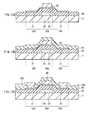
- FIG. 1is a cross-sectional view illustrating a configuration of a thin-film transistor according to a first embodiment.
- FIGS. 2A to 2Care cross-sectional views illustrating a manufacturing method of the thin-film transistor illustrated in FIG. 1 in order of process steps.
- FIGS. 3A to 3Care cross-sectional views illustrating process steps subsequent to those of FIGS. 2A to 2C .
- FIG. 4is a diagram representing a result of energy-dispersive X-ray spectroscopy analysis of a channel region and a low-resistance region.
- FIGS. 5A and 5Bare diagrams comparing characteristics of the thin-film transistor illustrated in FIG. 1 with those of an existing thin-film transistor.
- FIG. 6is a diagram representing a result of measurement of an aluminum concentration of a low-resistance region of a thin-film transistor according to a second embodiment.
- FIG. 7is a cross-sectional view illustrating a configuration of a thin-film transistor according to a first modification.
- FIGS. 8A to 8Care cross-sectional views illustrating a manufacturing method of the thin-film transistor illustrated in FIG. 7 in order of process steps.
- FIG. 9is a cross-sectional view illustrating a configuration of the thin-film transistor according to the second embodiment.
- FIGS. 10A to 10Dare cross-sectional views illustrating a manufacturing method of the thin-film transistor illustrated in FIG. 9 in order of process steps.
- FIGS. 11A to 11Care cross-sectional views illustrating process steps subsequent to those of FIGS. 10A to 10D .
- FIG. 12is a cross-sectional view illustrating a configuration of a thin-film transistor according to a second modification.
- FIGS. 13A to 13Care cross-sectional views illustrating a manufacturing method of the thin-film transistor illustrated in FIG. 12 in order of process steps.
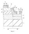
- FIG. 14is a cross-sectional view illustrating a configuration of a thin-film transistor according to a third embodiment.
- FIG. 15is a cross-sectional view illustrating an example of island-shaped high-resistance films.
- FIG. 16is a cross-sectional view illustrating another example of the island-shaped high-resistance films.
- FIG. 17is an explanatory view for describing sizes of the island-shaped high-resistance films.
- FIGS. 18A to 18Care cross-sectional views illustrating a manufacturing method of the thin-film transistor illustrated in FIG. 14 in order of process steps.
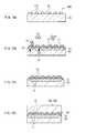
- FIGS. 19A to 19Dare cross-sectional views for describing the process steps illustrated in FIGS. 18A to 18C in detail.
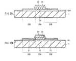
- FIG. 20illustrates the Thornton's model.
- FIGS. 21A and 21Bare diagrams comparing characteristics of the thin-film transistor illustrated in FIG. 14 with those of an existing thin-film transistor.
- FIGS. 22A and 22Bare diagrams each representing characteristics of a thin-film transistor when a thickness of a high-resistance film is varied.
- FIGS. 23A and 23Bare cross-sectional views illustrating a manufacturing method of a thin-film transistor according to a third modification in order of process steps.
- FIGS. 24A and 24Bare cross-sectional views illustrating process steps subsequent to those of FIGS. 23A and 23B .
- FIGS. 25A and 25Bare cross-sectional views illustrating a manufacturing method of a thin-film transistor according to a fourth modification in order of process steps.
- FIGS. 26A and 26Bare cross-sectional views illustrating process steps subsequent to those of FIGS. 25A and 25B .
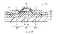
- FIG. 27is a cross-sectional view illustrating a configuration of a thin-film transistor according to a fourth embodiment.
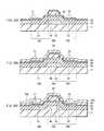
- FIGS. 28A to 28Dare cross-sectional views illustrating a manufacturing method of the thin-film transistor illustrated in FIG. 27 in order of process steps.
- FIGS. 29A to 29Care cross-sectional views illustrating process steps subsequent to those of FIGS. 28A to 28D .
- FIG. 30illustrates a configuration of a circuit of a display device according to a first application example.
- FIG. 31is an equivalent circuit diagram illustrating an example of a pixel driving circuit illustrated in FIG. 30 .
- FIG. 32is a perspective view illustrating an external appearance of a second application example.
- FIG. 33Ais a perspective view illustrating an external appearance of a third application example as viewed from a front side thereof
- FIG. 33Bis a perspective view illustrating the external appearance of the third application example as viewed from a back side thereof.
- FIG. 34is a perspective view illustrating an external appearance of a fourth application example.
- FIG. 35is a perspective view illustrating an external appearance of a fifth application example.
- FIG. 36Ais a front view in an open state of a sixth application example
- FIG. 36Bis a side view in the open state
- FIG. 36Cis a front view in a closed state
- FIG. 36Dis a left side view
- FIG. 36Eis a right side view
- FIG. 36Fis a top view
- FIG. 36Gis a bottom view.
- FIG. 37is a cross-sectional view illustrating a modification of the thin-film transistor illustrated in FIG. 1 .
- First Embodimentan embodiment of a top-gate thin-film transistor in which a low-resistance region is formed by utilizing oxidation of metal.
- Second Embodimentan embodiment of the top-gate thin-film transistor in which the low-resistance region is formed by utilizing dopant.
- First Modificationa modification of the top-gate thin-film transistor in which a high-resistance film is removed.
- Third Embodimentan embodiment of a bottom-gate thin-film transistor in which the high-resistance film is remained.
- Second Modificationa modification of the bottom-gate thin-film transistor in which the high-resistance film is removed.
- Fourth Embodimentan embodiment of the top-gate thin-film transistor in which the high-resistance film is formed in an island-like shape.
- Third Modificationa modification of a manufacturing method in which a metal film is patterned in an island-like shape and is then oxide to form the high-resistance film.
- Fourth Modificationa modification of the manufacturing method in which the metal film is oxide to form the high-resistance film and is then patterned in the island-like shape.
- FIG. 1illustrates a cross-sectional configuration of a thin-film transistor 1 according to a first embodiment.
- the thin-film transistor 1may be used as a drive element in a device such as a liquid crystal display and an organic EL display.
- the thin-film transistor 1may have a top-gate structure (or a staggered structure), in which an oxide semiconductor film 20 , a gate insulating film 30 , a gate electrode 40 , a high-resistance film 50 , an interlayer insulating film 60 , a source electrode 70 S, and a drain electrode 70 D are stacked in this order on a substrate 11 , for example.
- the substrate 11may be configured by a glass substrate, a plastic film, or other suitable member, for example.
- a material of a plasticcan be polyethylene terephthalate (PET), polyethylene naphthalate (PEN), or other suitable material.
- PETpolyethylene terephthalate
- PENpolyethylene naphthalate
- the plastic filmwhich is inexpensive, may be used in order to deposit the oxide semiconductor film 20 without heating the substrate 11 in a later-described sputtering process.
- the substrate 11may be a metal substrate depending on an application, such as a stainless steel (SUS).
- the oxide semiconductor film 20is provided on the substrate 11 in an island-like shape including the gate electrode 40 and peripheral sections of the gate electrode 40 , and functions as an active layer of the thin-film transistor 1 .
- the oxide semiconductor film 20may have a thickness of about 50 nm, for example, and has a channel region 20 A opposed to the gate electrode 40 .
- the gate insulating film 30 and the gate electrode 40are provided in this order and in the same shape on the channel region 20 A.
- a source region 20 Sis provided on one side of the channel region 20 A, and a drain region 20 D is provided on the other side of the channel region 20 A.
- the channel region 20 Ais configured by an oxide semiconductor.
- oxide semiconductorrefers to a compound including oxygen and one or more elements such as indium, gallium, zinc, and tin.
- the oxide semiconductorcan be an amorphous oxide semiconductor and a crystalline oxide semiconductor.
- the amorphous oxide semiconductorcan be indium gallium zinc oxide (IGZO).
- the crystalline oxide semiconductorcan be zinc oxide (ZnO), indium zinc oxide (IZO; Registered Trademark), indium gallium oxide (IGO), indium tin oxide (ITO), and indium oxide (InO).
- Each of the source region 20 S and the drain region 20 Dincludes a low-resistance region 21 in a partial region extending in a depth direction from an upper face thereof.
- the low-resistance region 21may have an oxygen concentration which is lower than that of the channel region 20 A, for example, and is thereby made low in resistance. This makes it possible for the thin-film transistor 1 to have a self-aligned structure, and to be able to stabilize its characteristics.
- the oxygen concentration of the low-resistance region 21be equal to or less than 30%, since a resistance increases when the oxygen concentration in the low-resistance region 21 exceeds 30%.
- a region other than the low-resistance region 21 of each of the source region 20 S and the drain region 20 Dis configured by an oxide semiconductor as with the channel region 20 A.
- a depth of the low-resistance region 21will be described later in detail.
- the gate insulating film 30may have a thickness of about 300 nm, for example.
- the gate insulating film 30may be a monolayer film, which can be a silicon dioxide film, a silicon nitride film, a silicon nitride oxide film, an aluminum oxide film, or other suitable film, or a multilayer film thereof.
- the silicon dioxide film or the aluminum oxide filmis preferable, in that the silicon dioxide film and the aluminum oxide film are difficult to reduce the oxide semiconductor film 20 .
- the gate electrode 40serves to apply a gate voltage to the thin-film transistor 1 , and to control an electron density in the oxide semiconductor film 20 with the gate voltage.
- the gate electrode 40is provided in a selective region on the substrate 11 .
- the gate electrode 40has a thickness of between 10 nm and 500 nm both inclusive, and preferably has a thickness of about 200 nm, and may be configured of molybdenum (Mo).
- Momolybdenum
- a material structuring the gate electrode 40be a metal having a low resistance, which can be aluminum (Al), copper (Cu), or other suitable metal, since the gate electrode 40 is desirably low in resistance.
- a multilayer film having a combination of a low-resistance layer and a barrier layeris also preferable, since this makes it possible to make the gate electrode 40 low in resistance.
- the low-resistance layercan be aluminum (Al), copper (Cu), or other suitable element
- the barrier layercan be titanium (Ti), molybdenum (Mo), or other suitable element.
- the high-resistance film 50is provided between the interlayer insulating film 60 and the oxide semiconductor film 20 , between the interlayer insulating film 60 and the gate insulating film 30 , and between the interlayer insulating film 60 and the gate electrode 40 .
- the high-resistance film 50is a metal film which serves as a source of supply of metal which is diffused into the low-resistance region 21 , and which is oxidized, in a later-described manufacturing process.
- the high-resistance film 50may be configured by titanium oxide, aluminum oxide, indium oxide, or other suitable oxide.
- the high-resistance film 50 made of titanium oxide, aluminum oxide, or indium oxidehas an excellent barrier property against outside air, and is thus able to reduce an influence of oxygen or moisture that changes electrical characteristics of the oxide semiconductor film 20 .
- providing of the high-resistance film 50makes it possible to stabilize electrical characteristics of the thin-film transistor 1 , and to further increase an effect achieved by the interlayer insulating film 60 .
- a thickness of the high-resistance film 50may be equal to or less than 20 nm, for example.
- the interlayer insulating film 60is provided on surfaces of the oxide semiconductor film 20 , the gate insulating film 30 , and the gate electrode 40 with the high-resistance film 50 in between.
- the interlayer insulating film 60may have a thickness of about 300 nm, for example.
- the interlayer insulating film 60may be configured of a monolayer film, which can be a silicon dioxide film, an aluminum oxide film, or other suitable film, or a multilayer film thereof.
- the multilayer film of the silicon dioxide film and the aluminum oxide filmmakes it possible to suppress incorporation or diffusion of moisture into the oxide semiconductor film 20 , and to further increase electrical stability and reliability of the thin-film transistor 1 .
- the source electrode 70 S and the drain electrode 70 Dare connected to the low-resistance region 21 through connection holes provided in the interlayer insulating film 60 and the high-resistance film 50 .
- the source electrode 70 S and the drain electrode 70 Deach may have a thickness of about 200 nm, and may be configured of molybdenum (Mo).
- Momolybdenum
- the source electrode 70 S and the drain electrode 70 Deach be configured by a metal (or a metal wiring) having a low resistance, which can be aluminum (Al), copper (Cu), or other suitable metal.
- a multilayer film having a combination of a low-resistance layer and a barrier layeris also preferable.
- the low-resistance layercan be aluminum (Al), copper (Cu), or other suitable element
- the barrier layercan be titanium (Ti), molybdenum (Mo), or other suitable element.
- each of the source electrode 70 S and the drain electrode 70 Dbe provided to evade or bypass a region immediately above the gate electrode 40 , since this enables to reduce parasitic capacitances formed in a cross region of the gate electrode 40 and the source electrode 70 S and in a cross region of the gate electrode 40 and the drain electrode 70 D.
- the thin-film transistor 1may be manufactured, for example, as follows.
- FIGS. 2A to 3Cillustrate a manufacturing method of the thin-film transistor 1 in order of process steps.
- the oxide semiconductor film 20made of the material described above, is formed at a thickness of about 50 nm on the entire surface of the substrate 11 with a sputtering method, for example.
- a ceramic targethaving the same composition as that of the oxide semiconductor film 20 to be formed is used.
- an oxygen partial pressureis so controlled that desired transistor characteristics are obtained, since a carrier concentration in the oxide semiconductor film 20 is largely dependent on the oxygen partial pressure in sputtering.
- the oxide semiconductor film 20is shaped in the island-like shape, which includes the channel region 20 A, the source region 20 S on one side thereof, and the drain region 20 D on the other side thereof, with photolithography and etching processes, for example.
- the oxide semiconductor film 20be processed with a wet-etching utilizing a mixture of phosphoric acid, nitric acid, and acetic acid.
- the use of the mixture of phosphoric acid, nitric acid, and acetic acidmakes it possible to sufficiently increase a selectivity ratio relative to an underlying substrate, and to process relatively easily.
- a gate insulating material film 30 Awhich can be the silicon dioxide film, the aluminum oxide film, or other suitable oxide film, is formed at a thickness of about 300 nm on the entire surfaces of the substrate 11 and the oxide semiconductor film 20 with a plasma chemical vapor deposition (CVD) method etc., for example.
- the silicon dioxide filmhere may be formed with a reactive-sputtering method, other than the plasma CVD method mentioned before.
- the aluminum oxide filmmay be formed with a reactive-sputtering method, a CVD method, or an atomic layer deposition method.
- a gate electrode material film 40 Awhich can be the monolayer film including molybdenum (Mo), titanium (Ti), aluminum (Al), or other suitable element, or the multilayer film thereof, is formed at a thickness of about 200 nm on the entire surface of the gate insulating material film 30 A with a sputtering method, for example.
- the gate electrode material film 40 Ais shaped into a desired shape with photolithography and etching processes, for example, to form the gate electrode 40 on the channel region 20 A of the oxide semiconductor film 20 .
- the gate electrode 40is utilized as a mask to etch the gate insulating material film 30 A so as to form the gate insulating film 30 .
- the oxide semiconductor film 20is configured by a crystalline material such as ZnO, IZO, and IGO, it is possible to use a chemical solution such as hydrofluoric acid to maintain a significantly large etching selectivity ratio and process easily, in etching the gate insulating material film 30 A.
- the gate insulating film 30 and the gate electrode 40are formed in this order and in the same shape on the channel region 20 A of the oxide semiconductor film 20 .
- a metal film 50 Aconfigured of a metal which reacts at a relatively low temperature with oxygen, such as titanium (Ti), aluminum (Al), and indium (In), is formed at a thickness of between 5 nm and 10 nm both inclusive on surfaces of the oxide semiconductor film 20 , the gate insulating film 30 , and the gate electrode 40 with a sputtering method, for example.
- a heat treatmentis performed to oxidize the metal film 50 A so as to form the high-resistance film 50 .
- This oxidation reaction of the metal film 50 Autilizes a part of oxygen included in the source region 20 S and the drain region 20 D.
- oxygen concentrations in the source region 20 S and the drain region 20 Dstart to decrease from the upper faces of the source region 20 S and the drain region 20 D that contact with the metal film 50 A as the oxidation of the metal film 50 A progresses.
- each of the source region 20 S and the drain region 20 Dextending in the depth direction from the upper face of each of the source region 20 S and the drain region 20 D, is formed with the low-resistance region 21 , which has the lower oxygen concentration than that of the channel region 20 A.
- FIG. 4represents a result of examination on dependence in the depth direction of the oxygen concentration in the channel region 20 A as well as the oxygen concentrations in the source region 20 S and the drain region 20 D using an energy-dispersive X-ray spectroscopy (EDX) method, after performing the heat treatment of the metal film 50 A as in the manufacturing method described above.
- a material of the oxide semiconductor film 20was IGZO, and the metal film 50 A was an aluminum film which had a thickness of 5 nm.
- the heat treatmentwas conducted with annealing at a temperature of 300 degrees centigrade.
- the oxygen concentrations in the source region 20 S and the drain region 20 Dare lower than the oxygen concentration in the channel region 20 A throughout in the depth direction.
- a difference between the oxygen concentration in the channel region 20 A and the oxygen concentrations in the source region 20 S and the drain region 20 Dis highly distinct in a region within the depth of 10 nm, in particular.
- the low-resistance region 21is a part of each of the source region 20 S and the drain region 20 D extending in the depth direction from the upper face thereof, which part, to be more specific, is the region within 10 nm in the depth direction from the upper face thereof.
- the heat treatment of the metal film 50 Abe performed with the annealing at a temperature of about 300 degrees centigrade as described above, for example.
- the annealingmay be performed under a gas atmosphere having an oxidizing property that includes oxygen etc. This makes it possible to prevent the oxygen concentration of the low-resistance region 21 from being too low and to supply enough oxygen to the oxide semiconductor film 20 . This in turn makes it possible to curtail an annealing process performed in a later process step, thereby allowing a simplified manufacturing process.
- a temperature of the substrate 11may be set at a relatively high temperature of about 200 degrees centigrade in the process step of forming the metal film 50 A illustrated in FIG. 3A , for example. This enables to form the low-resistance region 21 without performing the heat treatment illustrated in FIG. 3B . In this case, it is possible to reduce the carrier concentration in the oxide semiconductor film 20 to a level desirable for a transistor.
- the metal film 50 Abe formed at the thickness of 10 nm or less as described above. Allowing the thickness of the metal film 50 A to be equal to or less than 10 nm makes it possible to completely oxidize the metal film 50 A with the heat treatment. When the metal film 50 A is not completely oxidized, a process step of removing the metal film 50 A with etching may become desirable. The process step of removing with etching is unnecessary when the metal film 50 A is completely oxidized and thereby the high-resistance film 50 is obtained, making it possible to simplify the manufacturing process. The thickness of the high-resistance film 50 consequently becomes 20 nm or less when the metal film 50 A is formed at the thickness of 10 nm or less.
- the oxidationwith a method such as an oxidation under a vapor atmosphere and a plasma oxidation, as a method of oxidizing the metal film 50 A.
- the plasma oxidationcan be performed immediately before the formation of the interlayer insulating film 60 with the plasma CVD method in a later process step, and is thus advantageous in that the number of process steps does not have to be increased in particular.
- the plasma oxidationbe performed at conditions where the temperature of the substrate 11 is set at about 200 to 400 degrees centigrade, and where plasma is generated under a gas atmosphere containing oxygen such as oxygen and oxygen dinitride, for example, since this makes it possible to form the high-resistance film 50 having the excellent barrier property against outside air as described above.
- the high-resistance film 50is also formed on sections such as the gate insulating film 30 and the gate electrode 40 , other than on the source region 20 S and the drain region 20 D of the oxide semiconductor film 20 . However, remaining the high-resistance film 50 without removing the same with etching will not be a cause of a leakage current.
- the interlayer insulating film 60which can be the silicon dioxide film, the aluminum oxide film, or other suitable film, or the multilayer film thereof, is formed at the thickness described above on the high-resistance film 50 , for example.
- the silicon dioxide filmmay be formed with a plasma CVD method.
- the aluminum oxide filmbe formed with a reactive-sputtering method utilizing an aluminum target and a direct-current (DC) power or an alternating-current (AC) power, since this makes it possible to perform the deposition quickly.
- the connection holeis formed in each of the interlayer insulating film 60 and the high-resistance film 50 with photolithography and etching processes, for example.
- a filmwhich can be a molybdenum (Mo) film or other suitable film, is formed at a thickness of about 200 nm on the interlayer insulating film 60 with a sputtering method, for example, and photolithography and etching processes are performed to shape the same into a predetermined shape.
- the source electrode 70 S and the drain electrode 70 Dare connected to the low-resistance regions 21 as illustrated in FIG. 1 .
- the thin-film transistor 1 illustrated in FIG. 1is completed.
- a current(a drain current) is generated in the channel region 20 A of the oxide semiconductor film 20 when a voltage (a gate voltage), which is equal to or higher than a predetermined threshold voltage, is applied to the gate electrode 40 through an unillustrated wiring layer.
- a voltagea gate voltage
- at least a part of each of the source region 20 S and the drain region 20 D extending in the depth direction from the upper face of each of the source region 20 S and the drain region 20 Dis provided with the low-resistance region 21 , which is lower in oxygen concentration than that of the channel region 20 A.
- FIG. 5Brepresents a result of examination on transistor characteristics of the actually-fabricated thin-film transistor 1 having the low-resistance region 21 with the manufacturing method described in the foregoing.
- the metal film 50 Awas an aluminum film which had a thickness of 5 nm.
- the heat treatmentwas conducted with annealing at a temperature of 300 degrees centigrade under an oxygen atmosphere for one hour to form the low-resistance region 21 .
- an ON-current of a transistorwas increased by two digits or more in the thin-film transistor 1 in which the low-resistance region 21 was formed by the heat treatment of the metal film 50 A, as compared with the thin-film transistor in which the formation and the heat treatment of the metal film were not conducted.
- each of the source region 20 S and the drain region 20 D of the oxide semiconductor film 20 extending in the depth direction from the upper face of each of the source region 20 S and the drain region 20 Dis provided with the low-resistance region 21 having the lower oxygen concentration than that of the channel region 20 A.
- the thin-film transistor 1having the self-aligned structure in which the parasitic capacitance is reduced and having the stabilized characteristics, and to address attaining of larger screen, higher definition, and higher frame rate, when the thin-film transistor 1 described in the foregoing is used to configure an active-driving-type display.
- the gate insulating film 30 and the gate electrode 40are formed in this order and in the same shape on the channel region 20 A of the oxide semiconductor film 20 .
- the metal film 50 Ais formed on the oxide semiconductor film 20 , the gate insulating film 30 , and the gate electrode 40 .
- the heat treatmentis performed on the metal film 50 A to oxidize the metal film 50 A into the high-resistance film 50 , and to form the low-resistance region 21 having the lower oxygen concentration than that of the channel region 20 A in a part of each of the source region 20 S and the drain region 20 D extending in the depth direction from the upper face of each of the source region 20 S and the drain region 20 D.
- the low-resistance region 21is formed without using a process step having a large number of varying factors such a plasma process step. Hence, unlike existing techniques, it is possible to solve dependence of an element characteristic on the plasma process step, and to achieve a stable element characteristic.
- a thin-film transistor according to a second embodimenthas a similar configuration as that of the thin-film transistor 1 according to the first embodiment illustrated in FIG. 1 , except that a configuration and a manufacturing method of the low-resistance region 21 are different from those in the first embodiment described above. Note that the same or equivalent elements as those according to the first embodiment are denoted with the same reference numerals, and will not be described in detail. Also, process steps corresponding to those in the first embodiment will be described with reference to FIGS. 1 to 3C .
- the low-resistance region 21is made low in resistance by containing one or more elements selected from a group including aluminum (Al), boron (B), gallium (Ga), indium (In), titanium (Ti), silicon (Si), germanium (Ge), tin (Sn), and lead (Pb) as a dopant.
- Thin-film transistor 1is thereby able to have the self-aligned structure and to stabilize a characteristic.
- a dopant concentration, desirable for making the oxide semiconductor low in resistancein this case be equal to or more than 1 ⁇ 1019 cm-3.
- the low-resistance region 21may contain only one of the elements in the group described above, or may contain two or more elements. Also, it is preferable that the dopant concentration of the one or more elements included in the low-resistance region 21 be higher than that of the channel region 20 A.
- the thin-film transistor 1 according to the second embodimentmay be manufactured, for example, as follows.
- the oxide semiconductor film 20is formed with the process step illustrated in FIG. 2A .
- the gate insulating film 30 and the gate electrode 40are formed in this order and in the same shape on the channel region 20 A of the oxide semiconductor film 20 with the process steps illustrated in FIGS. 2B and 2C in a similar manner as in the first embodiment.
- the low-resistance region 21which contains, as a dopant, one or more elements selected from a group including aluminum (Al), boron (B), gallium (Ga), indium (In), titanium (Ti), silicon (Si), germanium (Ge), tin (Sn), and lead (Pb) in a part of each of the source region 20 S and the drain region 20 D extending in the depth direction from the upper face of each of the source region 20 S and the drain region 20 D.
- a groupincluding aluminum (Al), boron (B), gallium (Ga), indium (In), titanium (Ti), silicon (Si), germanium (Ge), tin (Sn), and lead (Pb) in a part of each of the source region 20 S and the drain region 20 D extending in the depth direction from the upper face of each of the source region 20 S and the drain region 20 D.
- the low-resistance region 21may be formed with the process steps illustrated in FIGS. 3A and 3B in a similar manner manner as in the first embodiment when the low-resistance region 21 contains aluminum (Al), indium (In), or titanium (Ti). More specifically, the metal film 50 A configured of aluminum (Al), indium (In), or titanium (Ti) as a dopant material film is formed on the surfaces of the oxide semiconductor film 20 , the gate insulating film 30 , and the gate electrode 40 . Then, the metal film 50 A is subjected to the heat treatment, by which the metal film 50 A is oxidized, and thus the high-resistance film 50 configured of aluminum oxide, indium oxide, or titanium oxide is formed.
- the low-resistance region 21which includes aluminum (Al), indium (In), or titanium (Ti), in a part of each of the source region 20 S and the drain region 20 D extending in the depth direction from the upper face thereof.
- the low-resistance region 21contains boron (B), gallium (Ga), silicon (Si), germanium (Ge), tin (Sn), or lead (Pb), the low-resistance region 21 may also be formed with the same process steps as those in the case of aluminum (Al), indium (In), or titanium (Ti). More specifically, the metal film or the nonmetal film 50 A configured of boron (B), gallium (Ga), silicon (Si), germanium (Ge), tin (Sn), or lead (Pb) as the dopant material film is formed on the surfaces of the oxide semiconductor film 20 , the gate insulating film 30 , and the gate electrode 40 .
- the metal film or the nonmetal film 50 Ais subjected to the heat treatment, by which the metal film or the nonmetal film 50 A is oxidized, and thus the high-resistance film 50 configured of boron oxide, gallium oxide, silicon dioxide, germanium oxide, tin oxide, or lead oxide is formed.
- the low-resistance region 21which includes boron (B), gallium (Ga), silicon (Si), germanium (Ge), tin (Sn), or lead (Pb), in a part of each of the source region 20 S and the drain region 20 D extending in the depth direction from the upper face thereof.
- FIG. 6represents a result of measurement of an aluminum concentration in the low-resistance region 21 with a secondary ion mass spectrometry (SIMS) method, by actually fabricating the low-resistance region 21 which includes aluminum (Al) as the dopant with the manufacturing method described in the foregoing. It can be seen from FIG. 6 that the highest concentration of aluminum is included in the vicinity of a surface of the oxide semiconductor, and that aluminum which is 1 ⁇ 1019 cm-3 or more is included in the oxide semiconductor even in a region 40 nm deep from the surface.
- SIMSsecondary ion mass spectrometry
- the interlayer insulating film 60is formed on the high-resistance film 50 with the process step illustrated in FIG. 3C , in a similar manner as in the first embodiment. Then, as illustrated in FIG. 1 , the connection hole is formed in each of the interlayer insulating film 60 and the high-resistance film 50 with photolithography and etching processes, for example.
- a filmwhich can be a molybdenum (Mo) film or other suitable film, is formed at a thickness of about 200 nm on the interlayer insulating film 60 with a sputtering method, for example, and photolithography and etching processes are performed to shape the same into a predetermined shape.
- the source electrode 70 S and the drain electrode 70 Dare connected to the low-resistance regions 21 as again illustrated in FIG. 1 .
- the thin-film transistor 1 illustrated in FIG. 1is completed.
- the current(the drain current) is generated in the channel region 20 A of the oxide semiconductor film 20 when the voltage (the gate voltage), which is equal to or higher than a predetermined threshold voltage, is applied to the gate electrode 40 , as in the first embodiment.
- each of the source region 20 S and the drain region 20 D extending in the depth direction from the upper face of each of the source region 20 S and the drain region 20 Dis provided with the low-resistance region 21 , which contains one or more elements selected from a group including aluminum (Al), boron (B), gallium (Ga), indium (In), titanium (Ti), silicon (Si), germanium (Ge), tin (Sn), and lead (Pb) as a dopant.
- Alaluminum
- Bboron
- Gagallium
- Inindium
- Tititanium
- Sisilicon
- germaniumgermanium
- Sngermanium
- Pblead
- each of the source region 20 S and the drain region 20 D of the oxide semiconductor film 20 extending in the depth direction from the upper face of each of the source region 20 S and the drain region 20 Dis provided with the low-resistance region 21 , which contains one or more elements selected from a group including aluminum (Al), boron (B), gallium (Ga), indium (In), titanium (Ti), silicon (Si), germanium (Ge), tin (Sn), and lead (Pb) as a dopant.
- the thin-film transistor 1having the self-aligned structure in which the parasitic capacitance is reduced and having the stabilized characteristics, and to address the attaining of larger screen, higher definition, and higher frame rate, when the thin-film transistor 1 described in the foregoing is used to configure an active-driving-type display.
- the gate insulating film 30 and the gate electrode 40are provided in this order and in the same shape on the channel region 20 A of the oxide semiconductor film 20 . Then, the metal film or the nonmetal film 50 A is formed as the dopant material film on the oxide semiconductor film 20 , the gate insulating film 30 , and the gate electrode 40 .
- the heat treatmentis performed on the metal film or the nonmetal film 50 A to oxidize the metal film or the nonmetal 50 A into the high-resistance film 50 , and to form the low-resistance region 21 , which contains one or more elements selected from a group including aluminum (Al), boron (B), gallium (Ga), indium (In), titanium (Ti), silicon (Si), germanium (Ge), tin (Sn), and lead (Pb) as a dopant, in a part of each of the source region 20 S and the drain region 20 D extending in the depth direction from the upper face of each of the source region 20 S and the drain region 20 D.
- the low-resistance region 21is formed without using a process step having a large number of varying factors such a plasma process step. Hence, unlike existing techniques, it is possible to solve dependence of an element characteristic on the plasma process step, and to achieve a stable element characteristic.
- FIG. 7illustrates a cross-sectional configuration of a thin-film transistor 1 A according to a first modification.
- the thin-film transistor 1 Ahas a configuration, an operation, and an effect, which are similar to those of the thin-film transistor 1 according to the first embodiment described above, except that the high-resistance film 50 is not provided so as to reduce a leakage current.
- the thin-film transistor 1 Amay be manufactured, for example, as follows. First, in a similar manner as in the first embodiment, the oxide semiconductor film 20 , the gate insulating film 30 , the gate electrode 40 , and the metal film 50 A are formed on the substrate 11 , and the metal film 50 A is subjected to the heat treatment to form the low-resistance region 21 and the high-resistance film 50 , with the process steps illustrated in FIGS. 2A to 3B . Then, as illustrated in FIG. 8A , the high-resistance film 50 is removed with etching.
- the use of a dry-etching method utilizing gas, which contains chlorine etc.makes it possible to easily remove the high-resistance film 50 as well as the metal film 50 A that has not been completely oxidized.
- the interlayer insulating film 60is formed in a similar manner as in the first embodiment.
- the connection holesare provided in the interlayer insulating film 60 , and the source electrode 70 S and the drain electrode 70 D are connected to the low-resistance regions 21 , in a similar manner as in the first embodiment.
- FIG. 9illustrates a cross-sectional configuration of a thin-film transistor 1 B according to a third embodiment.
- the thin-film transistor 1 Bhas a similar configuration as that of the thin-film transistor 1 according to the first embodiment described above, except that the thin-film transistor 1 B is a bottom-gate thin-film transistor in which the gate electrode 40 , the gate insulating film 30 , the oxide semiconductor film 20 , a channel protecting film 80 , the interlayer insulating film 60 , the source electrode 70 S, and the drain electrode 70 D are stacked in this order on the substrate 11 .
- the same or equivalent elements as those according to the first embodimentare denoted with the same reference numerals, and will not be described in detail.
- the channel protecting film 80is provided on the channel region 20 A of the oxide semiconductor film 20 .
- the channel protecting film 80may have a thickness of about 200 nm, and may be configured of a monolayer film, which can be a silicon dioxide film, a silicon nitride film, an aluminum oxide film, or other suitable film, or a multilayer film thereof, for example.
- the thin-film transistor 1 Bmay be manufactured, for example, as follows. Note that reference is made to the first embodiment to describe process steps that are same as those in the first embodiment.
- a filmwhich can be a molybdenum (Mo) film or other suitable film, is formed at a thickness of about 200 nm on the entire surface of the substrate 11 with a method such as a sputtering method and an evaporation method, for example.
- the molybdenum filmis patterned with a photolithography method, for example, to form the gate electrode 40 as illustrated in FIG. 10A .
- the gate insulating film 30which can be a silicon dioxide film, an aluminum oxide film, or other suitable film, is formed at a thickness of about 300 nm on the entire surface of the substrate 11 on which the gate electrode 40 is formed, with a plasma CVD method, for example.
- the oxide semiconductor film 20is formed on the gate insulating film 30 in a similar manner as in the first embodiment.
- a channel protecting material filmwhich can be a monolayer film of a silicon dioxide film, a silicon nitride film, an aluminum oxide film, or other suitable film, or a multilayer film thereof, is formed at a thickness of about 200 nm on the entire surfaces of the oxide semiconductor film 20 and the gate insulating film 30 .
- a back-side exposurein which the gate electrode 40 is utilized as a mask, is used to form the channel protecting film 80 at a position close to the gate electrode 40 in a self-aligned fashion.
- the metal film 50 Ais formed on the oxide semiconductor film 20 and the channel protecting film 80 in a similar manner as in the first embodiment.
- the heat treatmentis performed to oxidize the metal film 50 A so as to form the high-resistance film 50 , and to form the low-resistance region 21 having the lower oxygen concentration than that of the channel region 20 A in a part of each of the source region 20 S and the drain region 20 D extending in the depth direction from the upper face of each of the source region 20 S and the drain region 20 D.
- the interlayer insulating film 60is formed on the high-resistance film 50 in a similar manner as in the first embodiment.
- the connection holesare provided in each of the interlayer insulating film 60 and the high-resistance film 50 , and the source electrode 70 S and the drain electrode 70 D are connected to the low-resistance regions 21 , in a similar manner as in the first embodiment.
- the thin-film transistor 1 B illustrated in FIG. 9is completed.
- FIG. 12illustrates a cross-sectional configuration of a thin-film transistor 1 C according to a second modification.
- the thin-film transistor 1 Chas a configuration, an operation, and an effect, which are similar to those of the thin-film transistor 1 B according to the third embodiment described above, except that the high-resistance film 50 is not provided so as to reduce a leakage current.
- the thin-film transistor 1 Cmay be manufactured, for example, as follows. First, in a similar manner as in the third embodiment, the gate electrode 40 , the gate insulating film 30 , the oxide semiconductor film 20 , the channel protecting film 80 , and the metal film 50 A are formed on the substrate 11 , and the metal film 50 A is subjected to the heat treatment to form the low-resistance region 21 and the high-resistance film 50 , with the process steps illustrated in FIGS. 10A to 10D . Then, as illustrated in FIG. 13A , the high-resistance film 50 is removed with etching. Then, as illustrated in FIG. 13B , the interlayer insulating film 60 is formed in a similar manner as in the third embodiment.
- connection holesare provided in the interlayer insulating film 60 , and the source electrode 70 S and the drain electrode 70 D are connected to the low-resistance regions 21 , in a similar manner as in the third embodiment.
- FIG. 14illustrates a configuration of a thin-film transistor 1 D according to a fourth embodiment.
- the thin-film transistor 1 Dhas a similar configuration as that of the thin-film transistor 1 according to the first embodiment described above, except that the high-resistance film 50 is configured by a plurality of discontinuous island-shaped high-resistance films 51 .
- the same or equivalent elements as those according to the first embodimentare denoted with the same reference numerals, and will not be described in detail.
- Each of the island-shaped high-resistance films 51may be configured of aluminum oxide, for example.
- the island-shaped high resistance film 51does not necessarily have to be configured by aluminum oxide in its entirety in a thickness direction thereof.
- the island-shaped high resistance film 51may have a configuration in which only an upper surface thereof is configured of aluminum oxide as an oxidized section 53 A, and in which a section (or a lower part) other than the upper surface is configured of metallic aluminum as an unoxidized section 53 B.
- FIG. 15the island-shaped high resistance film 51 may have a configuration in which only an upper surface thereof is configured of aluminum oxide as an oxidized section 53 A, and in which a section (or a lower part) other than the upper surface is configured of metallic aluminum as an unoxidized section 53 B.
- the island-shaped high resistance film 51may have a configuration in which the upper surface and side faces thereof are each configured of aluminum oxide as the oxidized section 53 A, and in which a section (or a central part) other than the upper surface and the side faces is configured of metallic aluminum as the unoxidized section 53 B, for example.
- the clearance gap 52allows the adjacent island-shaped high-resistance films 51 to be physically separated from each other, and thereby each of the island-shaped high-resistance films 51 has an island-shaped configuration where the adjacent island-shaped high-resistance films 51 are not two-dimensionally connected to each other.
- the island-shaped high-resistance films 51hardly flow electricity in an in-plane direction mutually, making it possible to block the leakage current from the gate electrode 40 to the source electrode 70 S or from the gate electrode 40 to the drain electrode 70 D.
- Planar shapes of the island-shaped high-resistance films 51 and the clearance gap 52are not particularly limited.
- the island-shaped high-resistance film 51 and the clearance gap 52each may have an irregular planar shape.
- the plurality of island-shaped high-resistance films 51are separated from one another by the clearance gap 52 , at least at one position between the gate electrode 40 and the oxide semiconductor film 20 (side faces of the gate insulating film 30 ). In other words, it is preferable that side which is the longest among the island-shaped high-resistance films 51 be shorter in length than a thickness of the gate insulating film 30 .
- the thin-film transistor 1 Dmay be manufactured, for example, as follows.
- FIGS. 18A to 18Cillustrate a manufacturing method of the thin-film transistor 1 D illustrated in FIG. 14 in order of process steps. Note that reference is made to FIGS. 2A to 2C to describe process steps that are same as those in the first embodiment.
- the oxide semiconductor film 20is formed with the process step illustrated in FIG. 2A in a similar manner as in the first embodiment. Then, the gate insulating film 30 and the gate electrode 40 are formed in this order and in the same shape on the channel region 20 A of the oxide semiconductor film 20 with the process steps illustrated in FIGS. 2B and 2C in a similar manner as in the first embodiment.
- FIG. 18Athe metal film 50 A configured of the plurality of island-shaped metal films 51 A, which are made of aluminum (Al), is formed on the surfaces of the oxide semiconductor film 20 , the gate insulating film 30 , and the gate electrode 40 .
- FIG. 19Aschematically illustrates the metal film 50 A configured of the plurality of island-shaped metal films 51 A in an enlarged fashion. The clearance gaps 52 are generated among the plurality of island-shaped metal films 51 A.
- a method such as a vacuum evaporation method and a sputtering methodis suitable as a technique of forming the metal film 50 A.
- the most suitable technique for forming the metal film 50 A configured of the plurality of island-shaped metal films 51 Ais the sputtering method.
- FIG. 20represents the Thornton's model in a sputtering method, where T is a substrate temperature, and Tm is a melting point of a material.
- differences in crystallinity and grain size distribution of a to-be-formed filmoccur by varying a temperature of a substrate and a pressure of argon (Ar) serving as sputtering gas.
- a state referred to as “ZONE 3”is obtained when T/Tm is large and the pressure of argon is low, i.e., the energy of particles to be sputtered is extremely large and a metal film is easy to move on a substrate, by which an extremely dense film is formed.
- a state referred to as “ZONE 1”is obtained when T/Tm is small and the pressure of argon is high.
- the filmis rough even when the film is made very thick. That is, formation of the island-shaped films is possible in an early process of formation.
- the heat treatmentis performed in a similar manner as in the first embodiment to oxidize the plurality of island-shaped metal films 51 A of the metal film 50 A, by which the high-resistance film 50 having the plurality of island-shaped high-resistance film 51 configured of aluminum oxide is formed.
- Thisresults in the formation of the low-resistance region 21 , which includes aluminum as a dopant, or which has the lower oxygen concentration than that of the channel region 20 A, in a part of each of the source region 20 S and the drain region 20 D extending in the depth direction from the upper face thereof.
- FIG. 19Bschematically illustrates oxidation of the metal film 50 A in an enlarged fashion.
- the plurality of island-shaped metal films 51 A of the metal film 50 Aabsorb oxygen O2 in an atmosphere and oxygen O within the oxide semiconductor film 20 serving as an underlying layer, and are thereby oxidized.
- each of the island-shaped metal films 51 Aincreases in volume in accordance with an amount of oxygen absorbed.
- a surface area, which contacts with oxygen, of the metal film 50 A configured of the plurality of island-shaped metal films 51 Aincreases. Hence, the oxidation is further promoted, making it possible to suppress the leakage current also from this respect.
- the oxide semiconductor film 20the low-resistance region 21 is formed immediately below each of the island-like metal films 51 A.
- FIG. 19Cschematically illustrates, in an enlarged fashion, that the high-resistance film 50 configured of the plurality of island-shaped high-resistance films 51 is formed, and that the low-resistance region 21 is formed in the oxide semiconductor film 20 , by the oxidation of the metal film 50 A.
- the island-shaped high-resistance film 51expands by the oxidation, whereas the clearance gap 52 shrinks.
- the island-shaped high-resistance films 51there may be the island-shaped high-resistance film 51 which is separated from the adjacent island-shaped high-resistance film 51 by the clearance gap 52 , and there may also be the island-shaped high-resistance film 51 which is joined to the adjacent island-shaped high-resistance film 51 by disappearance of the clearance gap 52 .
- the interlayer insulating film 60is formed on the high-resistance film 50 in a similar manner as in the first embodiment. Then, as illustrated in FIG. 14 , the connection holes are formed in the interlayer insulating film 60 with photolithography and etching processes, for example.
- a filmwhich can be a molybdenum (Mo) film or other suitable film, is formed at a thickness of about 200 nm on the interlayer insulating film 60 with a sputtering method, for example, and photolithography and etching processes are performed to shape the same into a predetermined shape.
- the source electrode 70 S and the drain electrode 70 Dare connected to the low-resistance regions 21 as again illustrated in FIG. 14 .
- FIG. 19Dillustrates a state where the source electrode 70 S and the drain electrode 70 D are formed on the plurality of island-shaped high-resistance films 51 .
- the plurality of island-shaped high-resistance films 51are separated from one another by the clearance gaps 52 , so that the source electrode 70 S and the drain electrode 70 D are connected to the low-resistance regions 21 through the clearance gaps 52 .
- a contact resistance between the source electrode 70 S and the low-resistance region 21 , and that between the drain electrode 70 D and the low-resistance region 21are decreased, thereby making it possible to eliminate a process step of removing the island-shaped high-resistance films 51 on the low-resistance region 21 .
- the thin-film transistor 1 D illustrated in FIG. 14is completed.
- the current(the drain current) is generated in the channel region 20 A of the oxide semiconductor film 20 when the voltage (the gate voltage), which is equal to or higher than a predetermined threshold voltage, is applied to the gate electrode 40 , as in the first embodiment.
- the high-resistance film 50is configured by the plurality of discontinuous island-shaped high-resistance films 51 , and the adjacent island-shaped high-resistance films 51 are physically separated from each other by the clearance gap 52 . Hence, electricity hardly flows among the island-shaped high-resistance films 51 . Thus, the leakage current from the gate electrode 40 to the source electrode 70 S or from the gate electrode 40 to the drain electrode 70 D is blocked, making it possible to improve transistor characteristics.
- FIG. 21Arepresents a result of examination on transistor characteristics of the actually-fabricated thin-film transistor 1 D having the high-resistance film 50 configured of the plurality of island-shaped high-resistance films 51 with the manufacturing method described in the foregoing.
- a silicon dioxide (SiO2) filmwas first formed at a thickness of 200 nm as a buffer layer on the substrate 11 , made of a glass substrate, with a plasma-enhanced chemical vapor deposition (PECVD) method.
- PECVDplasma-enhanced chemical vapor deposition
- the oxide semiconductor film 20 made of an InGaZnO filmwas formed at a thickness of 40 nm.
- the metal film 50 A made of an aluminum filmwas formed at a thickness of 5 nm.
- the metal film 50 Awas deposited under deposition conditions where the substrate temperature was about 100 degrees centigrade and the argon pressure was about 0.5 PA. T/Tm in this case equals to 0.15 since the melting point of aluminum is about 660 degrees centigrade. Because the argon pressure was low, it was likely that the deposition was achieved under a state of “ZONE T (transition)” in the Thornton's model represented in FIG. 20 . However, examination on a cross-section of the deposited metal film 50 A confirmed that the plurality of discontinuous island-shaped metal films 51 A were formed.
- the depositionmay be achieved under the state of “ZONE 1”, and that the thickness of the metal film 50 A can be made thick. Then, the heat treatment was performed on the metal film 50 A at 300 degrees centigrade under an atmosphere containing about 30% of oxygen for one hour, to form the low-resistance region 21 .
- an ON-current of a transistorwas increased by two digits or more in the thin-film transistor 1 D, in which the low-resistance region 21 was formed and in which the high-resistance film 50 configured of the plurality of island-shaped high-resistance films 51 was formed by the heat treatment of the metal film 50 A configured of the plurality of island-shaped metal films 51 A, as compared with the thin-film transistor in which the formation and the heat treatment of the metal film were not conducted.
- FIGS. 22A and 22Beach represent a result of examination on a source-drain current Id and a gate-drain current Ig of the thin-film transistor 1 D, in which examinations the thin-film transistors 1 D, each having the high-resistance film 50 of different thickness by varying the thickness of the metal film 50 A at 5 nm or 10 nm, were fabricated.
- an OFF-state current of a transistoris large in the thin-film transistor 1 D having the 10 nm thick metal film 50 A as compared with the thin-film transistor 1 D having the 5 nm thick metal film 50 A, suggesting that there was a connection between the source electrode 70 S and the drain electrode 70 D.
- leakage currents denoted by Igare significantly large, meaning that the high-resistance film 50 obviously served as a leakage path.
- Igleakage currents denoted by forming the metal film 50 A at the thickness of 5 nm or less reduces the leakage and allows the transistor characteristics to be improved.
- the high-resistance film 50is configured by the plurality of island-shaped high-resistance films 51 .
- the contact resistance between the source electrode 70 S and the low-resistance region 21 , and that between the drain electrode 70 D and the low-resistance region 21are decreased, thereby eliminating the process step of removing the island-shaped high-resistance films 51 on the low-resistance region 21 .
- FIGS. 23A to 24Billustrate a manufacturing method of the thin-film transistor 1 D according to a third modification in order of process steps.
- the manufacturing method according to this modificationdiffers from that according to the fourth embodiment described above in a formation method of the high-resistance film 50 .
- FIGS. 2A to 2Cdescribe process steps that correspond to those in the first embodiment.
- the oxide semiconductor film 20is formed with the process step illustrated in FIG. 2A in a similar manner as in the first embodiment. Then, the gate insulating film 30 and the gate electrode 40 are formed in this order and in the same shape on the channel region 20 A of the oxide semiconductor film 20 with the process steps illustrated in FIGS. 2B and 2C in a similar manner as in the first embodiment.
- the metal film 50 A configured of aluminum (Al)is formed as an uniform continuous film on the surfaces of the oxide semiconductor film 20 , the gate insulating film 30 , and the gate electrode 40 .
- the metal film 50 Ais patterned with photolithography and etching processes, for example, to divide the metal film 50 A into the plurality of island-shaped metal films 51 A.
- the clearance gaps 52are provided among the plurality of island-shaped metal films 51 A, and these clearance gaps 52 are utilized to physically separate the plurality of island-shaped metal films 51 A from one another.
- the heat treatmentis performed in a similar manner as in the first embodiment to oxidize the plurality of island-shaped metal films 51 A of the metal film 50 A, by which the high-resistance film 50 having the plurality of island-shaped high-resistance film 51 configured of aluminum oxide is formed.
- Thisresults in the formation of the low-resistance region 21 , which includes aluminum as a dopant, or which has the lower oxygen concentration than that of the channel region 20 A, in a part of each of the source region 20 S and the drain region 20 D extending in the depth direction from the upper face thereof.
- the interlayer insulating film 60is formed on the high-resistance film 50 in a similar manner as in the first embodiment. Then, as illustrated in FIG. 14 , the connection holes are formed in the interlayer insulating film 60 with photolithography and etching processes, for example.
- a filmwhich can be a molybdenum (Mo) film or other suitable film, is formed at a thickness of about 200 nm on the interlayer insulating film 60 with a sputtering method, for example, and photolithography and etching processes are performed to shape the same into a predetermined shape.
- the source electrode 70 S and the drain electrode 70 Dare connected to the low-resistance regions 21 as again illustrated in FIG. 14 .
- the plurality of island-shaped high-resistance films 51are separated from one another by the clearance gaps 52 , so that the source electrode 70 S and the drain electrode 70 D are connected to the low-resistance regions 21 through the clearance gaps 52 .
- the contact resistance between the source electrode 70 S and the low-resistance region 21 , and that between the drain electrode 70 D and the low-resistance region 21 ,are decreased, thereby making it possible to eliminate the process step of removing the island-shaped high-resistance films 51 on the low-resistance region 21 .
- the thin-film transistor 1 D illustrated in FIG. 14is completed.
- FIGS. 25A to 26Billustrate a manufacturing method of the thin-film transistor 1 D according to a fourth modification in order of process steps.
- the manufacturing method according to this modificationdiffers from that according to the fourth embodiment described above in a formation method of the high-resistance film 50 .
- FIGS. 2A to 2Cdescribe process steps that correspond to those in the first embodiment.
- the oxide semiconductor film 20is formed with the process step illustrated in FIG. 2A in a similar manner as in the first embodiment. Then, the gate insulating film 30 and the gate electrode 40 are formed in this order and in the same shape on the channel region 20 A of the oxide semiconductor film 20 with the process steps illustrated in FIGS. 2B and 2C in a similar manner as in the first embodiment.
- the metal film 50 A configured of aluminum (Al)is formed as the uniform continuous film on the surfaces of the oxide semiconductor film 20 , the gate insulating film 30 , and the gate electrode 40 .
- the heat treatmentis performed in a similar manner as in the first embodiment to oxidize the metal film 50 A so as to form the high-resistance film 50 .
- Thisresults in the formation of the low-resistance region 21 , which includes aluminum as a dopant, or which has the lower oxygen concentration than that of the channel region 20 A, in a part of each of the source region 20 S and the drain region 20 D extending in the depth direction from the upper face thereof.
- the high-resistance film 50is patterned with photolithography and etching processes, for example, to divide the high-resistance film 50 into the plurality of island-shaped high-resistance films 51 .
- the clearance gaps 52are provided among the plurality of island-shaped high-resistance films 51 , and these clearance gaps 52 are utilized to physically separate the plurality of island-shaped high-resistance films 51 from one another.
- the interlayer insulating film 60is formed on the high-resistance film 50 in a similar manner as in the first embodiment. Then, as illustrated in FIG. 14 , the connection holes are formed in the interlayer insulating film 60 with photolithography and etching processes, for example.
- a filmwhich can be a molybdenum (Mo) film or other suitable film, is formed at a thickness of about 200 nm on the interlayer insulating film 60 with a sputtering method, for example, and photolithography and etching processes are performed to shape the same into a predetermined shape.
- the source electrode 70 S and the drain electrode 70 Dare connected to the low-resistance regions 21 as again illustrated in FIG. 14 .
- the plurality of island-shaped high-resistance films 51are separated from one another by the clearance gaps 52 , so that the source electrode 70 S and the drain electrode 70 D are connected to the low-resistance regions 21 through the clearance gaps 52 .
- the contact resistance between the source electrode 70 S and the low-resistance region 21 , and that between the drain electrode 70 D and the low-resistance region 21 ,are decreased, thereby making it possible to eliminate the process step of removing the island-shaped high-resistance films 51 on the low-resistance region 21 .
- the thin-film transistor 1 D illustrated in FIG. 14is completed.
- FIG. 27illustrates a cross-sectional configuration of a thin-film transistor 1 E according to a fifth embodiment.
- the thin-film transistor 1 Ehas a similar configuration as that of each of the thin-film transistors 1 B and 1 D according to the third and the fourth embodiments described above, except that the thin-film transistor 1 E is a bottom-gate thin-film transistor in which the gate electrode 40 , the gate insulating film 30 , the oxide semiconductor film 20 , the channel protecting film 80 , the interlayer insulating film 60 , the source electrode 70 S, and the drain electrode 70 D are stacked in this order on the substrate 11 .
- the same or equivalent elements as those according to the third and the fourth embodimentsare denoted with the same reference numerals, and will not be described in detail.
- the thin-film transistor 1 Emay be manufactured, for example, as follows. Note that reference is made to the first embodiment or the third embodiment to describe process steps that are same as those in the first embodiment or the third embodiment.
- the gate electrode 40 and the gate insulating film 30are formed in order on the substrate 11 with the process step illustrated in FIG. 10A in a similar manner as in the third embodiment.
- the oxide semiconductor film 20is formed on the gate insulating film 30 with the process step illustrated in FIG. 10B in a similar manner as in the third embodiment.
- the channel protecting film 80is formed on the oxide semiconductor film 20 with the process step illustrated in FIG. 10C in a similar manner as in the third embodiment.
- the metal film 50 A configured of the plurality of island-shaped metal films 51 Ais formed on the oxide semiconductor film 20 , the channel protecting film 80 , and the gate insulating film 30 with the process step illustrated in FIG. 18A in a similar manner as in the fourth embodiment.
- the heat treatmentis performed in a similar manner as in the fourth embodiment to oxidize the plurality of island-shaped metal films 51 A of the metal film 50 A with the process step illustrated in FIG. 18B so as to form the high-resistance film 50 configured of the plurality of island-shaped high-resistance films 51 .
- Thisresults in the formation of the low-resistance region 21 , having the lower oxygen concentration than that of the channel region 20 A, in a part or in the entire part of each of the source region 20 S and the drain region 20 D extending in the depth direction from the upper face thereof.
- the interlayer insulating film 60is formed on the high-resistance film 50 in a similar manner as in the first embodiment.
- connection holesare provided in the interlayer insulating film 60 , and the source electrode 70 S and the drain electrode 70 D are connected to the low-resistance regions 21 , in a similar manner as in the first embodiment.
- the thin-film transistor 1 E illustrated in FIG. 27is completed.
- FIG. 30illustrates a configuration of a circuit of a display device 90 provided with any one of the thin-film transistors 1 to 1 E as a drive element.
- the display device 90may be a display such as a liquid crystal display and an organic EL display, for example.
- the display device 90is provided, on a drive panel 91 , with a plurality of pixels 10 R, 10 G, and 10 B which are arranged in matrix, and various driving circuits for driving those pixels 10 R, 10 G, and 10 B.
- the pixels 10 R, 10 G, and 10 Bmay be elements, such as liquid crystal display elements and organic EL elements, which emit lights for red, green, and blue, respectively, although the number of colors and the types of colors are not limited thereto.
- These three pixels 10 R, 10 G, and 10 Bare grouped as a single pixel to configure a displaying region 110 having a plurality of such pixels.
- a signal line driving circuit 120 and a scanning line driving circuit 130each serving as a driver for image displaying
- a pixel driving circuit 150which are provided as the driving circuits, for example.
- An unillustrated sealing panelis attached to the drive panel 91 , by which sealing panel the pixels 10 R, 10 G, and 10 B, and the driving circuits are sealed.
- FIG. 31is an equivalent circuit diagram of the pixel driving circuit 150 .
- the pixel driving circuit 150is an active-type driving circuit in which transistors Tr 1 and Tr 2 are arranged. Each of the transistors Tr 1 and Tr 2 is any one of the thin-film transistors 1 to 1 E described above. A capacitor Cs is provided between the transistors Tr 1 and Tr 2 .
- the pixel 10 R(or the pixel 10 G or 10 B) is connected in series to the transistor Tr 1 between a first power source line (Vcc) and a second power source line (GND).
- the pixel driving circuit 150is further provided with a plurality of signal lines 120 A arranged in columns, and a plurality of scanning lines 130 A arranged in rows.
- Each of the signal lines 120 Ais connected to the signal line driving circuit 120 , from which circuit image signals are supplied to source electrodes of the transistors Tr 2 through the signal lines 120 A.
- Each of the scanning lines 130 Ais connected to the scanning line driving circuit 130 , from which circuit scanning signals are sequentially supplied to gate electrodes of the transistors Tr 2 through the scanning lines 130 A.
- each of the transistors Tr 1 and Tr 2is configured by any one of the thin-film transistors 1 to 1 E according to the embodiments and the modifications. Hence, it is possible to perform high-quality displaying by any one of the thin-film transistors 1 to 1 E having a reduced parasitic capacitance by a self-aligned structure and having stabilized characteristics.
- Such a display device 90may be employed in any electronic devices, such as those according to second to sixth application examples as follows, for example.
- FIG. 32illustrates an external appearance of a television device.
- the television deviceis provided with an image display screen unit 300 including a front panel 310 and a filter glass 320 , for example.
- FIGS. 33A and 33Beach illustrate an external appearance of a digital camera.
- the digital camerais provided with a light emitting unit 410 for flash, a display unit 420 , a menu switch section 430 , and a shutter-release button 440 , for example.
- FIG. 34illustrates an external appearance of laptop personal computer.
- the laptop personal computeris provided with a body 510 , a keyboard 520 for input-manipulation of characters and the like, and a display unit 530 for displaying an image, for example.
- FIG. 35illustrates an external appearance of a video camera.
- the video camerais provided with a body 610 , a lens 620 provided in a front face of the body 610 for picking-up an image of an object, a shooting start/stop switch 630 , and a display unit 640 , for example.
- FIGS. 36A to 36Geach illustrate an external appearance of a cellular phone.
- the cellular phonecouples an upper casing 710 and a lower casing 720 through a coupling part (or a hinge) 730 , and is provided with a display 740 , a sub-display 750 , a picture light 760 , and a camera 770 , for example.
- the present applicationhas been described in the foregoing by way of example with reference to the embodiments, the modifications, and the application examples, the present application is not limited thereto but may be modified in a wide variety of ways.
- a part of each of the source region 20 S and the drain region 20 D extending in the depth direction from the upper face of each of the source region 20 S and the drain region 20 Dis provided with the low-resistance region 21 .
- the low-resistance region 21may be provided in at least a part of each of the source region 20 S and the drain region 20 D extending in the depth direction from the upper face of each of the source region 20 S and the drain region 20 D.
- the low-resistance region 21may be provided in the entire part of each of the source region 20 S and the drain region 20 D extending in the depth direction from the upper face of each of the source region 20 S and the drain region 20 D.
- the oxide semiconductor film 20is provided directly on the substrate 11 .
- the oxide semiconductor film 20may be provided on the substrate 11 with an insulating film such as a silicon dioxide film, a silicon nitride film, and an aluminum oxide film in between. This makes it possible to suppress diffusion of an influential factor, such as impurity and moisture, from the substrate 11 into the oxide semiconductor film 20 .
- materials and thicknesses of various layers, deposition methods, and deposition conditionsare illustrative, and not limitative. Other materials, thicknesses, deposition methods, and deposition conditions may be employed.
- the present applicationis applicable to display devices utilizing other display elements, such as inorganic EL elements, electrodeposition-type display elements, and electrochromic-type display elements.
Landscapes
- Thin Film Transistor (AREA)
- Liquid Crystal (AREA)
- Devices For Indicating Variable Information By Combining Individual Elements (AREA)
Abstract
Description
- The present application claims priority to Japanese Priority Patent Application Nos. JP 2010-079293 and JP 2010-245035 filed in the Japan Patent Office on Mar. 30, 2010 and Nov. 1, 2010, respectively, the entire contents of which are hereby incorporated by reference.
- The present application relates to a thin-film transistor using an oxide semiconductor, to a method of manufacturing the same, and to a display device provided with the thin-film transistor.
- An active-driving-type liquid crystal display device and an active-driving-type organic electroluminescence (hereinafter simply referred to as “EL”) display device each use a thin-film transistor (TFT) as a drive element, and each cause an electric charge, which corresponds to a signal voltage for writing an image, to be held in a hold capacitor. However, when a parasitic capacitance generated in a cross region of a gate electrode and a source electrode, or of the gate electrode and a drain electrode of the thin-film transistor is large, the signal voltage may fluctuate, leading to an occurrence of image degradation.
- In the organic EL display device, in particular, it is necessary to increase the hold capacitor when the parasitic capacitance is large, and a proportion of wiring etc. occupying a pixel layout is large. As a result, there is more chance of short-circuit between the wirings etc., and there rises an issue that a fabrication yield is decreased.
- To address these disadvantages, an attempt has been made to reduce the parasitic capacitance formed in the cross region of the gate electrode and the source electrode or the drain electrode, in the thin-film transistor in which an oxide semiconductor such as zinc oxide (ZnO) and indium gallium zinc oxide (IGZO) is used for a channel.
- For example, Japanese Unexamined Patent Application Publication No. 2007-220817 (JP2007-220817A) and J. Park et al. “Self-aligned top-gate amorphous gallium indium zinc oxide thin film transistors”, Applied Physics Letters, American Institute of Physics, 93, 053501 (2008) (Non-Patent Document 1) each disclose a self-aligned top-gate thin-film transistor. In each of the disclosed thin-film transistors, a gate electrode and a gate insulating film are formed to have the same shape on a channel region of an oxide semiconductor thin-film layer, and a region of the oxide semiconductor thin-film layer uncovered by the gate electrode and the gate insulating film is then made low in resistance to form a source-drain region. Also, R. Hayashi et al. “Improved Amorphous In—Ga—Zn—O TFTs”,
SID 08 DIGEST, 42. 1, 621-624 (2008) (Non-Patent Document 2) discloses a bottom-gate thin-film transistor having a self-aligned structure, which forms a source region and a drain region in an oxide semiconductor film with a back-side exposure in which a gate electrode is utilized as a mask. - Techniques disclosed in JP2007-220817A and the Non-Patent
Document 2 each form a silicon nitride film serving as an interlayer insulating film with a plasma chemical vapor deposition (CVD) method, and each introduce hydrogen included in the silicon nitride film into an oxide semiconductor thin-film layer, to form a low-resistance source-drain region in a self-aligned fashion. The technique disclosed in JP2007-220817A further uses a plasma process utilizing hydrogen gas in combination with the introduction of hydrogen from the silicon nitride film. Also, a technique disclosed in the Non-PatentDocument 1 exposes an oxide semiconductor film under a plasma atmosphere utilizing argon gas to form a low-resistance source-drain region. Existing techniques including those disclosed in JP2007-220817A andNon-Patent Documents - It is desirable to provide a thin-film transistor, a method of manufacturing the same, and a display device provided with the thin-film transistor, capable of stabilizing a characteristic of a thin-film transistor having a self-aligned structure.
- In the thin-film transistor according to this embodiment, at least a part of each of the source region and the drain region extending in the depth direction from the upper face of each of the source region and the drain region is provided with the low-resistance region, which includes, as a dopant, one or more elements selected from the group consisting of aluminum, boron, gallium, indium, titanium, silicon, germanium, tin, and lead. Hence, an element characteristic is stabilized.
- In the thin-film transistor according to this embodiment, at least a part of each of the source region and the drain region extending in the depth direction from the upper face of each of the source region and the drain region is provided with the low-resistance region, which includes the oxygen concentration which is lower than the oxygen concentration of the channel region. Hence, an element characteristic is stabilized.
- In an embodiment, a thin film transistor is provided. The thin film transistor includes an oxide semiconductor layer including a source region, a drain region, and a channel region wherein a portion of the source and drain regions has an oxygen concentration less than the channel region.
- In an embodiment, the portion of the source and drain regions is a low-resistance region extending in a depth direction from an upper face thereof.
- In an embodiment, the low-resistance region extends within 10 nm in the depth direction from the upper face thereof.
- In an embodiment, a high-resistance material layer is provided that is formed on at least the portion of the source and drain regions.
- In an embodiment, the high-resistance material layer is selected from the group consisting of titanium oxide, aluminum oxide, and indium oxide.
- In an embodiment, the high-resistance material layer includes a plurality of island-shaped metal films.
- In an embodiment, the island-shaped metal films are spaced apart so as to provide a clearance gap.
- In an embodiment, the portion of the source and drain regions is a low-resistance region extending in a depth direction from an upper face thereof, and wherein a first portion of the island-shaped metal films is in contact with the low resistance region and a second portion of the island-shaped metal films is in contact with a gate electrode.
- In an embodiment, the thin film transistor further includes an insulating layer.
- In an embodiment, the thin film transistor further includes a source electrode and a drain electrode.
- In an embodiment, the thin film transistor is configured as any one of a top gate structure and a bottom gate structure.
- In an embodiment, a thin film transistor is provided. The thin film transistor includes an oxide semiconductor layer including a source region, a drain region, and a channel region, wherein a portion of the source and drain regions includes a dopant selected from the group consisting of aluminum, boron, gallium, indium, titanium, silicon, germanium, tin, lead, and combinations thereof.
- In an embodiment, the portion of the source and drain regions is a low-resistance region extending in a depth direction from an upper face thereof.
- In an embodiment, the low-resistance region extends at least within 30 nm in the depth direction from the upper face thereof.
- In an embodiment, the thin film transistor further includes a high-resistance material layer that is formed on at least the portion of the source and drain regions.
- In an embodiment, the high-resistance material layer includes a constituent selected from the group consisting of titanium, aluminum, and indium, boron, gallium, silicon, germanium, tin, and lead.
- In an embodiment, the high-resistance material layer includes any one of a plurality of island-shaped metal films and a plurality of island-shaped nonmetal films.
- In an embodiment, any one of the island-shaped metal films and the island-shaped nonmetal films are spaced apart so as to provide a clearance gap.
- In an embodiment, the portion of the source and drain regions is a low-resistance region extending in a depth direction from an upper face thereof, and wherein a first portion of any one of the island-shaped metal films and the island-shaped nonmetal films is in contact with the low resistance region and a second portion of any one of the island-shaped metal films and the island-shaped nonmetal films is in contact with a gate electrode.
- In an embodiment, the thin film transistor further includes an insulating layer.
- In an embodiment, the thin film transistor further includes a source electrode and a drain electrode.
- In an embodiment, the thin film transistor is configured as any one of a top gate structure and a bottom gate structure.
- In an embodiment, a method of manufacturing a thin film transistor is provided. The method includes forming an oxide semiconductor layer including a source region, a drain region, and a channel region, wherein a portion of the source and drain regions includes an oxygen concentration less than the channel region.
- In an embodiment, the portion of the source and drain regions is a low-resistance region.
- In an embodiment, the method further includes forming a metal layer; and heat treating the metal layer thereby forming the low-resistance region.
- In an embodiment, the metal layer is heat treated at an annealing temperature.
- In an embodiment, the method further includes removing the metal layer subsequent to heat treatment.
- In an embodiment, the metal layer includes a plurality of island-shaped metal films.
- In an embodiment, wherein the metal layer is formed on the source and drain regions.
- In an embodiment, the method further includes forming an insulating layer.
- In an embodiment, the method further includes a source electrode and a drain electrode.
- In an embodiment, the thin film transistor is configured as any one of a bottom gate structure and a top gate structure.
- In yet another embodiment, a method of manufacturing a thin film transistor is provided. The method including forming an oxide semiconductor layer including a source region, a drain region, and a channel region, wherein a portion of the source and drain regions includes a dopant selected from the group consisting of aluminum, boron, gallium, indium, titanium, silicon, germanium, tin, lead, and combinations thereof.
- In an embodiment, the portion of the source and drain regions is a low-resistance region.
- In an embodiment, the method further includes forming any one of a metal layer and a nonmetal layer; and heat treating any one of the metal layer and the nonmetal layer thereby forming the low-resistance region.
- In an embodiment, the method further includes removing any one of the metal layer and the nonmetal layer subsequent to heat treatment.
- In an embodiment, the metal layer includes a plurality of island-shaped metal films and the nonmetal layer includes a plurality of island-shaped nonmetal films.
- In an embodiment, any one of the metal layer and the nonmetal layer is formed on the source and drain regions.
- In an embodiment, the method further includes forming an insulating layer.
- In an embodiment, the method further includes forming a source electrode and a drain electrode.
- In an embodiment, the thin film transistor is configured as any one of a bottom gate structure and a top gate structure.
- According to each of the thin-film transistors of the embodiments, the low-resistance region, which includes one or more elements selected from the group consisting of aluminum, boron, gallium, indium, titanium, silicon, germanium, tin, and lead as a dopant, or includes the oxygen concentration which is lower than the oxygen concentration of the channel region, is provided in at least a part of each of the source region and the drain region extending in the depth direction from the upper face of each of the source region and the drain region. Hence, it is possible to stabilize a characteristic of the thin-film transistor having the self-aligned structure. Therefore, when the thin-film transistor is used to configure the display device, it is possible to achieve high-quality displaying by the thin-film transistor, having the self-aligned structure in which the parasitic capacitance is reduced and having the stabilized characteristic.
- According to each of the methods of manufacturing the thin-film transistor of the embodiments, the gate insulating film and the gate electrode are formed in this order and in the same shape on the channel region of the oxide semiconductor film. Then, the metal film or the nonmetal film serving as the dopant material film is formed on the oxide semiconductor film, the gate insulating film, and the gate electrode. Then, the heat treatment is performed to oxidize the metal film or the nonmetal film serving as the dopant material film into the high-resistance film, and to form the low-resistance region including, as a dopant, one or more elements selected from the group consisting of aluminum, boron, gallium, indium, titanium, silicon, germanium, tin, and lead, or including the oxygen concentration which is lower than the oxygen concentration of the channel region, in at least a part of each of the source region and the drain region extending in the depth direction from the upper face of each of the source region and the drain region. Hence, it is possible to form the low-resistance region without using a process step having a large number of varying factors such a plasma process step. Therefore, unlike existing techniques, it is possible to solve dependence of an element characteristic on the plasma process step, and to achieve a stable element characteristic.
- Additional features and advantages are described herein, and will be apparent from the following Detailed Description and the figures.
FIG. 1 is a cross-sectional view illustrating a configuration of a thin-film transistor according to a first embodiment.FIGS. 2A to 2C are cross-sectional views illustrating a manufacturing method of the thin-film transistor illustrated inFIG. 1 in order of process steps.FIGS. 3A to 3C are cross-sectional views illustrating process steps subsequent to those ofFIGS. 2A to 2C .FIG. 4 is a diagram representing a result of energy-dispersive X-ray spectroscopy analysis of a channel region and a low-resistance region.FIGS. 5A and 5B are diagrams comparing characteristics of the thin-film transistor illustrated inFIG. 1 with those of an existing thin-film transistor.FIG. 6 is a diagram representing a result of measurement of an aluminum concentration of a low-resistance region of a thin-film transistor according to a second embodiment.FIG. 7 is a cross-sectional view illustrating a configuration of a thin-film transistor according to a first modification.FIGS. 8A to 8C are cross-sectional views illustrating a manufacturing method of the thin-film transistor illustrated inFIG. 7 in order of process steps.FIG. 9 is a cross-sectional view illustrating a configuration of the thin-film transistor according to the second embodiment.FIGS. 10A to 10D are cross-sectional views illustrating a manufacturing method of the thin-film transistor illustrated inFIG. 9 in order of process steps.FIGS. 11A to 11C are cross-sectional views illustrating process steps subsequent to those ofFIGS. 10A to 10D .FIG. 12 is a cross-sectional view illustrating a configuration of a thin-film transistor according to a second modification.FIGS. 13A to 13C are cross-sectional views illustrating a manufacturing method of the thin-film transistor illustrated inFIG. 12 in order of process steps.FIG. 14 is a cross-sectional view illustrating a configuration of a thin-film transistor according to a third embodiment.FIG. 15 is a cross-sectional view illustrating an example of island-shaped high-resistance films.FIG. 16 is a cross-sectional view illustrating another example of the island-shaped high-resistance films.FIG. 17 is an explanatory view for describing sizes of the island-shaped high-resistance films.FIGS. 18A to 18C are cross-sectional views illustrating a manufacturing method of the thin-film transistor illustrated inFIG. 14 in order of process steps.FIGS. 19A to 19D are cross-sectional views for describing the process steps illustrated inFIGS. 18A to 18C in detail.FIG. 20 illustrates the Thornton's model.FIGS. 21A and 21B are diagrams comparing characteristics of the thin-film transistor illustrated inFIG. 14 with those of an existing thin-film transistor.FIGS. 22A and 22B are diagrams each representing characteristics of a thin-film transistor when a thickness of a high-resistance film is varied.FIGS. 23A and 23B are cross-sectional views illustrating a manufacturing method of a thin-film transistor according to a third modification in order of process steps.FIGS. 24A and 24B are cross-sectional views illustrating process steps subsequent to those ofFIGS. 23A and 23B .FIGS. 25A and 25B are cross-sectional views illustrating a manufacturing method of a thin-film transistor according to a fourth modification in order of process steps.FIGS. 26A and 26B are cross-sectional views illustrating process steps subsequent to those ofFIGS. 25A and 25B .FIG. 27 is a cross-sectional view illustrating a configuration of a thin-film transistor according to a fourth embodiment.FIGS. 28A to 28D are cross-sectional views illustrating a manufacturing method of the thin-film transistor illustrated inFIG. 27 in order of process steps.FIGS. 29A to 29C are cross-sectional views illustrating process steps subsequent to those ofFIGS. 28A to 28D .FIG. 30 illustrates a configuration of a circuit of a display device according to a first application example.FIG. 31 is an equivalent circuit diagram illustrating an example of a pixel driving circuit illustrated inFIG. 30 .FIG. 32 is a perspective view illustrating an external appearance of a second application example.FIG. 33A is a perspective view illustrating an external appearance of a third application example as viewed from a front side thereof, andFIG. 33B is a perspective view illustrating the external appearance of the third application example as viewed from a back side thereof.FIG. 34 is a perspective view illustrating an external appearance of a fourth application example.FIG. 35 is a perspective view illustrating an external appearance of a fifth application example.FIG. 36A is a front view in an open state of a sixth application example,FIG. 36B is a side view in the open state,FIG. 36C is a front view in a closed state,FIG. 36D is a left side view,FIG. 36E is a right side view,FIG. 36F is a top view, andFIG. 36G is a bottom view.FIG. 37 is a cross-sectional view illustrating a modification of the thin-film transistor illustrated inFIG. 1 .- The present application will be described in detail with reference to the accompanying drawings according to an embodiment. The description will be given in the following order.
- 1. First Embodiment: an embodiment of a top-gate thin-film transistor in which a low-resistance region is formed by utilizing oxidation of metal.
- 2. Second Embodiment: an embodiment of the top-gate thin-film transistor in which the low-resistance region is formed by utilizing dopant.
- 3. First Modification: a modification of the top-gate thin-film transistor in which a high-resistance film is removed.
- 4. Third Embodiment: an embodiment of a bottom-gate thin-film transistor in which the high-resistance film is remained.
- 5. Second Modification: a modification of the bottom-gate thin-film transistor in which the high-resistance film is removed.
- 6. Fourth Embodiment: an embodiment of the top-gate thin-film transistor in which the high-resistance film is formed in an island-like shape.
- 7. Third Modification: a modification of a manufacturing method in which a metal film is patterned in an island-like shape and is then oxide to form the high-resistance film.
- 8. Fourth Modification: a modification of the manufacturing method in which the metal film is oxide to form the high-resistance film and is then patterned in the island-like shape.
- 9. Fifth Embodiment: an embodiment of the bottom-gate thin-film transistor in which the high-resistance film is formed in the island-like shape.
- 10. Application Examples.
FIG. 1 illustrates a cross-sectional configuration of a thin-film transistor 1 according to a first embodiment. The thin-film transistor 1 may be used as a drive element in a device such as a liquid crystal display and an organic EL display. The thin-film transistor 1 may have a top-gate structure (or a staggered structure), in which anoxide semiconductor film 20, agate insulating film 30, agate electrode 40, a high-resistance film 50, aninterlayer insulating film 60, asource electrode 70S, and adrain electrode 70D are stacked in this order on asubstrate 11, for example.- The
substrate 11 may be configured by a glass substrate, a plastic film, or other suitable member, for example. A material of a plastic can be polyethylene terephthalate (PET), polyethylene naphthalate (PEN), or other suitable material. The plastic film, which is inexpensive, may be used in order to deposit theoxide semiconductor film 20 without heating thesubstrate 11 in a later-described sputtering process. Thesubstrate 11 may be a metal substrate depending on an application, such as a stainless steel (SUS). - The
oxide semiconductor film 20 is provided on thesubstrate 11 in an island-like shape including thegate electrode 40 and peripheral sections of thegate electrode 40, and functions as an active layer of the thin-film transistor 1. Theoxide semiconductor film 20 may have a thickness of about 50 nm, for example, and has achannel region 20A opposed to thegate electrode 40. Thegate insulating film 30 and thegate electrode 40 are provided in this order and in the same shape on thechannel region 20A. Asource region 20S is provided on one side of thechannel region 20A, and adrain region 20D is provided on the other side of thechannel region 20A. - The
channel region 20A is configured by an oxide semiconductor. As used herein, the term “oxide semiconductor” refers to a compound including oxygen and one or more elements such as indium, gallium, zinc, and tin. The oxide semiconductor can be an amorphous oxide semiconductor and a crystalline oxide semiconductor. The amorphous oxide semiconductor can be indium gallium zinc oxide (IGZO). The crystalline oxide semiconductor can be zinc oxide (ZnO), indium zinc oxide (IZO; Registered Trademark), indium gallium oxide (IGO), indium tin oxide (ITO), and indium oxide (InO). - Each of the
source region 20S and thedrain region 20D includes a low-resistance region 21 in a partial region extending in a depth direction from an upper face thereof. The low-resistance region 21 may have an oxygen concentration which is lower than that of thechannel region 20A, for example, and is thereby made low in resistance. This makes it possible for the thin-film transistor 1 to have a self-aligned structure, and to be able to stabilize its characteristics. - It is desirable that the oxygen concentration of the low-
resistance region 21 be equal to or less than 30%, since a resistance increases when the oxygen concentration in the low-resistance region 21 exceeds 30%. - A region other than the low-
resistance region 21 of each of thesource region 20S and thedrain region 20D is configured by an oxide semiconductor as with thechannel region 20A. A depth of the low-resistance region 21 will be described later in detail. - The
gate insulating film 30 may have a thickness of about 300 nm, for example. Thegate insulating film 30 may be a monolayer film, which can be a silicon dioxide film, a silicon nitride film, a silicon nitride oxide film, an aluminum oxide film, or other suitable film, or a multilayer film thereof. In particular, the silicon dioxide film or the aluminum oxide film is preferable, in that the silicon dioxide film and the aluminum oxide film are difficult to reduce theoxide semiconductor film 20. - The
gate electrode 40 serves to apply a gate voltage to the thin-film transistor 1, and to control an electron density in theoxide semiconductor film 20 with the gate voltage. Thegate electrode 40 is provided in a selective region on thesubstrate 11. For example, thegate electrode 40 has a thickness of between 10 nm and 500 nm both inclusive, and preferably has a thickness of about 200 nm, and may be configured of molybdenum (Mo). It is preferable that a material structuring thegate electrode 40 be a metal having a low resistance, which can be aluminum (Al), copper (Cu), or other suitable metal, since thegate electrode 40 is desirably low in resistance. A multilayer film having a combination of a low-resistance layer and a barrier layer is also preferable, since this makes it possible to make thegate electrode 40 low in resistance. The low-resistance layer can be aluminum (Al), copper (Cu), or other suitable element, and the barrier layer can be titanium (Ti), molybdenum (Mo), or other suitable element. - The high-
resistance film 50 is provided between the interlayer insulatingfilm 60 and theoxide semiconductor film 20, between the interlayer insulatingfilm 60 and thegate insulating film 30, and between the interlayer insulatingfilm 60 and thegate electrode 40. The high-resistance film 50 is a metal film which serves as a source of supply of metal which is diffused into the low-resistance region 21, and which is oxidized, in a later-described manufacturing process. The high-resistance film 50 may be configured by titanium oxide, aluminum oxide, indium oxide, or other suitable oxide. The high-resistance film 50 made of titanium oxide, aluminum oxide, or indium oxide has an excellent barrier property against outside air, and is thus able to reduce an influence of oxygen or moisture that changes electrical characteristics of theoxide semiconductor film 20. Hence, providing of the high-resistance film 50 makes it possible to stabilize electrical characteristics of the thin-film transistor 1, and to further increase an effect achieved by theinterlayer insulating film 60. A thickness of the high-resistance film 50 may be equal to or less than 20 nm, for example. - The
interlayer insulating film 60 is provided on surfaces of theoxide semiconductor film 20, thegate insulating film 30, and thegate electrode 40 with the high-resistance film 50 in between. Theinterlayer insulating film 60 may have a thickness of about 300 nm, for example. Theinterlayer insulating film 60 may be configured of a monolayer film, which can be a silicon dioxide film, an aluminum oxide film, or other suitable film, or a multilayer film thereof. In particular, the multilayer film of the silicon dioxide film and the aluminum oxide film makes it possible to suppress incorporation or diffusion of moisture into theoxide semiconductor film 20, and to further increase electrical stability and reliability of the thin-film transistor 1. - The
source electrode 70S and thedrain electrode 70D are connected to the low-resistance region 21 through connection holes provided in theinterlayer insulating film 60 and the high-resistance film 50. Thesource electrode 70S and thedrain electrode 70D each may have a thickness of about 200 nm, and may be configured of molybdenum (Mo). As in thegate electrode 40, it is preferable that thesource electrode 70S and thedrain electrode 70D each be configured by a metal (or a metal wiring) having a low resistance, which can be aluminum (Al), copper (Cu), or other suitable metal. A multilayer film having a combination of a low-resistance layer and a barrier layer is also preferable. The low-resistance layer can be aluminum (Al), copper (Cu), or other suitable element, and the barrier layer can be titanium (Ti), molybdenum (Mo), or other suitable element. The use of such a multilayer film makes it possible to perform driving having reduced wiring delay. - It is desirable that each of the
source electrode 70S and thedrain electrode 70D be provided to evade or bypass a region immediately above thegate electrode 40, since this enables to reduce parasitic capacitances formed in a cross region of thegate electrode 40 and thesource electrode 70S and in a cross region of thegate electrode 40 and thedrain electrode 70D. - The thin-
film transistor 1 may be manufactured, for example, as follows. FIGS. 2A to 3C illustrate a manufacturing method of the thin-film transistor 1 in order of process steps. First, theoxide semiconductor film 20, made of the material described above, is formed at a thickness of about 50 nm on the entire surface of thesubstrate 11 with a sputtering method, for example. Herein, a ceramic target having the same composition as that of theoxide semiconductor film 20 to be formed is used. Also, an oxygen partial pressure is so controlled that desired transistor characteristics are obtained, since a carrier concentration in theoxide semiconductor film 20 is largely dependent on the oxygen partial pressure in sputtering.- Then, as illustrated in
FIG. 2A , theoxide semiconductor film 20 is shaped in the island-like shape, which includes thechannel region 20A, thesource region 20S on one side thereof, and thedrain region 20D on the other side thereof, with photolithography and etching processes, for example. Herein, it is preferable that theoxide semiconductor film 20 be processed with a wet-etching utilizing a mixture of phosphoric acid, nitric acid, and acetic acid. The use of the mixture of phosphoric acid, nitric acid, and acetic acid makes it possible to sufficiently increase a selectivity ratio relative to an underlying substrate, and to process relatively easily. - Then, as illustrated in
FIG. 2B , a gate insulatingmaterial film 30A, which can be the silicon dioxide film, the aluminum oxide film, or other suitable oxide film, is formed at a thickness of about 300 nm on the entire surfaces of thesubstrate 11 and theoxide semiconductor film 20 with a plasma chemical vapor deposition (CVD) method etc., for example. The silicon dioxide film here may be formed with a reactive-sputtering method, other than the plasma CVD method mentioned before. The aluminum oxide film may be formed with a reactive-sputtering method, a CVD method, or an atomic layer deposition method. - Thereafter, referring again to
FIG. 2B , a gateelectrode material film 40A, which can be the monolayer film including molybdenum (Mo), titanium (Ti), aluminum (Al), or other suitable element, or the multilayer film thereof, is formed at a thickness of about 200 nm on the entire surface of the gate insulatingmaterial film 30A with a sputtering method, for example. - As illustrated in
FIG. 2C , after forming the gateelectrode material film 40A, the gateelectrode material film 40A is shaped into a desired shape with photolithography and etching processes, for example, to form thegate electrode 40 on thechannel region 20A of theoxide semiconductor film 20. - Thereafter, referring again to
FIG. 2C , thegate electrode 40 is utilized as a mask to etch the gate insulatingmaterial film 30A so as to form thegate insulating film 30. Herein, when theoxide semiconductor film 20 is configured by a crystalline material such as ZnO, IZO, and IGO, it is possible to use a chemical solution such as hydrofluoric acid to maintain a significantly large etching selectivity ratio and process easily, in etching the gate insulatingmaterial film 30A. Thereby, thegate insulating film 30 and thegate electrode 40 are formed in this order and in the same shape on thechannel region 20A of theoxide semiconductor film 20. - As illustrated in
FIG. 3A , after forming thegate insulating film 30 and thegate electrode 40, ametal film 50A, configured of a metal which reacts at a relatively low temperature with oxygen, such as titanium (Ti), aluminum (Al), and indium (In), is formed at a thickness of between 5 nm and 10 nm both inclusive on surfaces of theoxide semiconductor film 20, thegate insulating film 30, and thegate electrode 40 with a sputtering method, for example. - As illustrated in
FIG. 3B , after forming themetal film 50A, a heat treatment is performed to oxidize themetal film 50A so as to form the high-resistance film 50. This oxidation reaction of themetal film 50A utilizes a part of oxygen included in thesource region 20S and thedrain region 20D. Hence, oxygen concentrations in thesource region 20S and thedrain region 20D start to decrease from the upper faces of thesource region 20S and thedrain region 20D that contact with themetal film 50A as the oxidation of themetal film 50A progresses. Thereby, a part of each of thesource region 20S and thedrain region 20D, extending in the depth direction from the upper face of each of thesource region 20S and thedrain region 20D, is formed with the low-resistance region 21, which has the lower oxygen concentration than that of thechannel region 20A. FIG. 4 represents a result of examination on dependence in the depth direction of the oxygen concentration in thechannel region 20A as well as the oxygen concentrations in thesource region 20S and thedrain region 20D using an energy-dispersive X-ray spectroscopy (EDX) method, after performing the heat treatment of themetal film 50A as in the manufacturing method described above. A material of theoxide semiconductor film 20 was IGZO, and themetal film 50A was an aluminum film which had a thickness of 5 nm. The heat treatment was conducted with annealing at a temperature of 300 degrees centigrade.- As can be seen from
FIG. 4 , the oxygen concentrations in thesource region 20S and thedrain region 20D are lower than the oxygen concentration in thechannel region 20A throughout in the depth direction. Above all, a difference between the oxygen concentration in thechannel region 20A and the oxygen concentrations in thesource region 20S and thedrain region 20D is highly distinct in a region within the depth of 10 nm, in particular. In other words, it indicates that the low-resistance region 21 is a part of each of thesource region 20S and thedrain region 20D extending in the depth direction from the upper face thereof, which part, to be more specific, is the region within 10 nm in the depth direction from the upper face thereof. - It is preferable that the heat treatment of the
metal film 50A be performed with the annealing at a temperature of about 300 degrees centigrade as described above, for example. Herein, the annealing may be performed under a gas atmosphere having an oxidizing property that includes oxygen etc. This makes it possible to prevent the oxygen concentration of the low-resistance region 21 from being too low and to supply enough oxygen to theoxide semiconductor film 20. This in turn makes it possible to curtail an annealing process performed in a later process step, thereby allowing a simplified manufacturing process. - Also, a temperature of the
substrate 11 may be set at a relatively high temperature of about 200 degrees centigrade in the process step of forming themetal film 50A illustrated inFIG. 3A , for example. This enables to form the low-resistance region 21 without performing the heat treatment illustrated inFIG. 3B . In this case, it is possible to reduce the carrier concentration in theoxide semiconductor film 20 to a level desirable for a transistor. - It is preferable that the
metal film 50A be formed at the thickness of 10 nm or less as described above. Allowing the thickness of themetal film 50A to be equal to or less than 10 nm makes it possible to completely oxidize themetal film 50A with the heat treatment. When themetal film 50A is not completely oxidized, a process step of removing themetal film 50A with etching may become desirable. The process step of removing with etching is unnecessary when themetal film 50A is completely oxidized and thereby the high-resistance film 50 is obtained, making it possible to simplify the manufacturing process. The thickness of the high-resistance film 50 consequently becomes 20 nm or less when themetal film 50A is formed at the thickness of 10 nm or less. - Herein, other than the heat treatment, it is also possible to promote the oxidation with a method such as an oxidation under a vapor atmosphere and a plasma oxidation, as a method of oxidizing the
metal film 50A. In particular, the plasma oxidation can be performed immediately before the formation of theinterlayer insulating film 60 with the plasma CVD method in a later process step, and is thus advantageous in that the number of process steps does not have to be increased in particular. It is preferable that the plasma oxidation be performed at conditions where the temperature of thesubstrate 11 is set at about 200 to 400 degrees centigrade, and where plasma is generated under a gas atmosphere containing oxygen such as oxygen and oxygen dinitride, for example, since this makes it possible to form the high-resistance film 50 having the excellent barrier property against outside air as described above. - It is to be noted that the high-
resistance film 50 is also formed on sections such as thegate insulating film 30 and thegate electrode 40, other than on thesource region 20S and thedrain region 20D of theoxide semiconductor film 20. However, remaining the high-resistance film 50 without removing the same with etching will not be a cause of a leakage current. - As illustrated in
FIG. 3C , after forming the low-resistance region 21, theinterlayer insulating film 60, which can be the silicon dioxide film, the aluminum oxide film, or other suitable film, or the multilayer film thereof, is formed at the thickness described above on the high-resistance film 50, for example. Herein, the silicon dioxide film may be formed with a plasma CVD method. It is preferable that the aluminum oxide film be formed with a reactive-sputtering method utilizing an aluminum target and a direct-current (DC) power or an alternating-current (AC) power, since this makes it possible to perform the deposition quickly. - Then, as illustrated in
FIG. 1 , the connection hole is formed in each of theinterlayer insulating film 60 and the high-resistance film 50 with photolithography and etching processes, for example. Then, a film, which can be a molybdenum (Mo) film or other suitable film, is formed at a thickness of about 200 nm on theinterlayer insulating film 60 with a sputtering method, for example, and photolithography and etching processes are performed to shape the same into a predetermined shape. Thereby, thesource electrode 70S and thedrain electrode 70D are connected to the low-resistance regions 21 as illustrated inFIG. 1 . Thus, the thin-film transistor 1 illustrated inFIG. 1 is completed. - In this thin-
film transistor 1, a current (a drain current) is generated in thechannel region 20A of theoxide semiconductor film 20 when a voltage (a gate voltage), which is equal to or higher than a predetermined threshold voltage, is applied to thegate electrode 40 through an unillustrated wiring layer. Herein, at least a part of each of thesource region 20S and thedrain region 20D extending in the depth direction from the upper face of each of thesource region 20S and thedrain region 20D is provided with the low-resistance region 21, which is lower in oxygen concentration than that of thechannel region 20A. Hence, an element characteristic is stabilized. FIG. 5B represents a result of examination on transistor characteristics of the actually-fabricated thin-film transistor 1 having the low-resistance region 21 with the manufacturing method described in the foregoing. Themetal film 50A was an aluminum film which had a thickness of 5 nm. The heat treatment was conducted with annealing at a temperature of 300 degrees centigrade under an oxygen atmosphere for one hour to form the low-resistance region 21.- Meanwhile, another thin-film transistor was fabricated without performing the formation and the heat treatment of the metal film to examine transistor characteristics thereof, a result of which is represented in
FIG. 5A . Herein, a plasma treatment was not performed. - As can be seen from
FIGS. 5A and 5B , an ON-current of a transistor was increased by two digits or more in the thin-film transistor 1 in which the low-resistance region 21 was formed by the heat treatment of themetal film 50A, as compared with the thin-film transistor in which the formation and the heat treatment of the metal film were not conducted. In other words, the examinations indicated that it is possible to achieve the thin-film transistor 1 having a reduced parasitic capacitance by a self-aligned structure and having stabilized element characteristics, by providing the low-resistance region 21 which includes aluminum as a dopant, or which has the lower oxygen concentration than that of thechannel region 20A, in at least a part of each of thesource region 20S and thedrain region 20D of theoxide semiconductor film 20 extending in the depth direction from the upper face thereof. - Thus, in the thin-
film transistor 1 according to this embodiment, at least a part of each of thesource region 20S and thedrain region 20D of theoxide semiconductor film 20 extending in the depth direction from the upper face of each of thesource region 20S and thedrain region 20D is provided with the low-resistance region 21 having the lower oxygen concentration than that of thechannel region 20A. Thereby, a characteristic of a top-gate thin-film transistor having a self-aligned structure is stabilized. Hence, it is possible to achieve high-quality displaying by the thin-film transistor 1 having the self-aligned structure in which the parasitic capacitance is reduced and having the stabilized characteristics, and to address attaining of larger screen, higher definition, and higher frame rate, when the thin-film transistor 1 described in the foregoing is used to configure an active-driving-type display. Also, it is possible to apply a layout having a smaller hold capacitor, and to reduce a proportion of wiring etc. occupying a pixel layout. Hence, it is possible to reduce a probability of occurrence of defects caused by short-circuit between the wirings etc., and to increase a fabrication yield. - According to the manufacturing method of the thin-
film transistor 1 of this embodiment, thegate insulating film 30 and thegate electrode 40 are formed in this order and in the same shape on thechannel region 20A of theoxide semiconductor film 20. Then, themetal film 50A is formed on theoxide semiconductor film 20, thegate insulating film 30, and thegate electrode 40. Then, the heat treatment is performed on themetal film 50A to oxidize themetal film 50A into the high-resistance film 50, and to form the low-resistance region 21 having the lower oxygen concentration than that of thechannel region 20A in a part of each of thesource region 20S and thedrain region 20D extending in the depth direction from the upper face of each of thesource region 20S and thedrain region 20D. Thereby, the low-resistance region 21 is formed without using a process step having a large number of varying factors such a plasma process step. Hence, unlike existing techniques, it is possible to solve dependence of an element characteristic on the plasma process step, and to achieve a stable element characteristic. - A thin-film transistor according to a second embodiment has a similar configuration as that of the thin-
film transistor 1 according to the first embodiment illustrated inFIG. 1 , except that a configuration and a manufacturing method of the low-resistance region 21 are different from those in the first embodiment described above. Note that the same or equivalent elements as those according to the first embodiment are denoted with the same reference numerals, and will not be described in detail. Also, process steps corresponding to those in the first embodiment will be described with reference toFIGS. 1 to 3C . - In the thin-film transistor according to this embodiment, the low-
resistance region 21 is made low in resistance by containing one or more elements selected from a group including aluminum (Al), boron (B), gallium (Ga), indium (In), titanium (Ti), silicon (Si), germanium (Ge), tin (Sn), and lead (Pb) as a dopant. Thin-film transistor 1 is thereby able to have the self-aligned structure and to stabilize a characteristic. - Herein, it is possible to increase an electron density in an oxide semiconductor when an element such as aluminum (Al), boron (B), gallium (Ga), indium (In), titanium (Ti), silicon (Si), germanium (Ge), tin (Sn), and lead (Pb) is present in the oxide semiconductor since such an element acts as a dopant, and thereby to make the oxide semiconductor low in resistance. It is preferable that a dopant concentration, desirable for making the oxide semiconductor low in resistance, in this case be equal to or more than 1×1019 cm-3.
- The low-
resistance region 21 may contain only one of the elements in the group described above, or may contain two or more elements. Also, it is preferable that the dopant concentration of the one or more elements included in the low-resistance region 21 be higher than that of thechannel region 20A. - The thin-
film transistor 1 according to the second embodiment may be manufactured, for example, as follows. - First, in a similar manner as in the first embodiment, the
oxide semiconductor film 20 is formed with the process step illustrated inFIG. 2A . Then, thegate insulating film 30 and thegate electrode 40 are formed in this order and in the same shape on thechannel region 20A of theoxide semiconductor film 20 with the process steps illustrated inFIGS. 2B and 2C in a similar manner as in the first embodiment. - Then, the low-
resistance region 21, which contains, as a dopant, one or more elements selected from a group including aluminum (Al), boron (B), gallium (Ga), indium (In), titanium (Ti), silicon (Si), germanium (Ge), tin (Sn), and lead (Pb) in a part of each of thesource region 20S and thedrain region 20D extending in the depth direction from the upper face of each of thesource region 20S and thedrain region 20D. - The low-
resistance region 21 may be formed with the process steps illustrated inFIGS. 3A and 3B in a similar manner manner as in the first embodiment when the low-resistance region 21 contains aluminum (Al), indium (In), or titanium (Ti). More specifically, themetal film 50A configured of aluminum (Al), indium (In), or titanium (Ti) as a dopant material film is formed on the surfaces of theoxide semiconductor film 20, thegate insulating film 30, and thegate electrode 40. Then, themetal film 50A is subjected to the heat treatment, by which themetal film 50A is oxidized, and thus the high-resistance film 50 configured of aluminum oxide, indium oxide, or titanium oxide is formed. This in turn results in the formation of the low-resistance region 21, which includes aluminum (Al), indium (In), or titanium (Ti), in a part of each of thesource region 20S and thedrain region 20D extending in the depth direction from the upper face thereof. - When the low-
resistance region 21 contains boron (B), gallium (Ga), silicon (Si), germanium (Ge), tin (Sn), or lead (Pb), the low-resistance region 21 may also be formed with the same process steps as those in the case of aluminum (Al), indium (In), or titanium (Ti). More specifically, the metal film or thenonmetal film 50A configured of boron (B), gallium (Ga), silicon (Si), germanium (Ge), tin (Sn), or lead (Pb) as the dopant material film is formed on the surfaces of theoxide semiconductor film 20, thegate insulating film 30, and thegate electrode 40. Then, the metal film or thenonmetal film 50A is subjected to the heat treatment, by which the metal film or thenonmetal film 50A is oxidized, and thus the high-resistance film 50 configured of boron oxide, gallium oxide, silicon dioxide, germanium oxide, tin oxide, or lead oxide is formed. This in turn results in the formation of the low-resistance region 21, which includes boron (B), gallium (Ga), silicon (Si), germanium (Ge), tin (Sn), or lead (Pb), in a part of each of thesource region 20S and thedrain region 20D extending in the depth direction from the upper face thereof. FIG. 6 represents a result of measurement of an aluminum concentration in the low-resistance region 21 with a secondary ion mass spectrometry (SIMS) method, by actually fabricating the low-resistance region 21 which includes aluminum (Al) as the dopant with the manufacturing method described in the foregoing. It can be seen fromFIG. 6 that the highest concentration of aluminum is included in the vicinity of a surface of the oxide semiconductor, and that aluminum which is 1×1019 cm-3 or more is included in the oxide semiconductor even in aregion 40 nm deep from the surface.- After forming the low-
resistance region 21, theinterlayer insulating film 60 is formed on the high-resistance film 50 with the process step illustrated inFIG. 3C , in a similar manner as in the first embodiment. Then, as illustrated inFIG. 1 , the connection hole is formed in each of theinterlayer insulating film 60 and the high-resistance film 50 with photolithography and etching processes, for example. - Then, a film, which can be a molybdenum (Mo) film or other suitable film, is formed at a thickness of about 200 nm on the
interlayer insulating film 60 with a sputtering method, for example, and photolithography and etching processes are performed to shape the same into a predetermined shape. Thereby, thesource electrode 70S and thedrain electrode 70D are connected to the low-resistance regions 21 as again illustrated inFIG. 1 . Thus, the thin-film transistor 1 illustrated inFIG. 1 is completed. - In this thin-
film transistor 1, the current (the drain current) is generated in thechannel region 20A of theoxide semiconductor film 20 when the voltage (the gate voltage), which is equal to or higher than a predetermined threshold voltage, is applied to thegate electrode 40, as in the first embodiment. Herein, at least a part of each of thesource region 20S and thedrain region 20D extending in the depth direction from the upper face of each of thesource region 20S and thedrain region 20D is provided with the low-resistance region 21, which contains one or more elements selected from a group including aluminum (Al), boron (B), gallium (Ga), indium (In), titanium (Ti), silicon (Si), germanium (Ge), tin (Sn), and lead (Pb) as a dopant. Hence, an element characteristic is stabilized. - Thus, in the thin-
film transistor 1 according to the second embodiment, at least a part of each of thesource region 20S and thedrain region 20D of theoxide semiconductor film 20 extending in the depth direction from the upper face of each of thesource region 20S and thedrain region 20D is provided with the low-resistance region 21, which contains one or more elements selected from a group including aluminum (Al), boron (B), gallium (Ga), indium (In), titanium (Ti), silicon (Si), germanium (Ge), tin (Sn), and lead (Pb) as a dopant. Thereby, a characteristic of a top-gate thin-film transistor having a self-aligned structure is stabilized. Hence, it is possible to achieve high-quality displaying by the thin-film transistor 1 having the self-aligned structure in which the parasitic capacitance is reduced and having the stabilized characteristics, and to address the attaining of larger screen, higher definition, and higher frame rate, when the thin-film transistor 1 described in the foregoing is used to configure an active-driving-type display. Also, it is possible to apply a layout having a smaller hold capacitor, and to reduce a proportion of wiring etc. occupying a pixel layout. Hence, it is possible to reduce a probability of occurrence of defects caused by short-circuit between the wirings etc., and to increase a fabrication yield. - According to the manufacturing method of the thin-
film transistor 1 of the second embodiment, thegate insulating film 30 and thegate electrode 40 are provided in this order and in the same shape on thechannel region 20A of theoxide semiconductor film 20. Then, the metal film or thenonmetal film 50A is formed as the dopant material film on theoxide semiconductor film 20, thegate insulating film 30, and thegate electrode 40. Then, the heat treatment is performed on the metal film or thenonmetal film 50A to oxidize the metal film or thenonmetal 50A into the high-resistance film 50, and to form the low-resistance region 21, which contains one or more elements selected from a group including aluminum (Al), boron (B), gallium (Ga), indium (In), titanium (Ti), silicon (Si), germanium (Ge), tin (Sn), and lead (Pb) as a dopant, in a part of each of thesource region 20S and thedrain region 20D extending in the depth direction from the upper face of each of thesource region 20S and thedrain region 20D. Thereby, the low-resistance region 21 is formed without using a process step having a large number of varying factors such a plasma process step. Hence, unlike existing techniques, it is possible to solve dependence of an element characteristic on the plasma process step, and to achieve a stable element characteristic. - [First Modification]
FIG. 7 illustrates a cross-sectional configuration of a thin-film transistor1A according to a first modification. The thin-film transistor1A has a configuration, an operation, and an effect, which are similar to those of the thin-film transistor 1 according to the first embodiment described above, except that the high-resistance film 50 is not provided so as to reduce a leakage current.- The thin-film transistor1A may be manufactured, for example, as follows. First, in a similar manner as in the first embodiment, the
oxide semiconductor film 20, thegate insulating film 30, thegate electrode 40, and themetal film 50A are formed on thesubstrate 11, and themetal film 50A is subjected to the heat treatment to form the low-resistance region 21 and the high-resistance film 50, with the process steps illustrated inFIGS. 2A to 3B . Then, as illustrated inFIG. 8A , the high-resistance film 50 is removed with etching. Herein, the use of a dry-etching method utilizing gas, which contains chlorine etc., makes it possible to easily remove the high-resistance film 50 as well as themetal film 50A that has not been completely oxidized. Then, as illustrated inFIG. 8B , theinterlayer insulating film 60 is formed in a similar manner as in the first embodiment. Then, as illustrated inFIG. 8C , the connection holes are provided in theinterlayer insulating film 60, and thesource electrode 70S and thedrain electrode 70D are connected to the low-resistance regions 21, in a similar manner as in the first embodiment. FIG. 9 illustrates a cross-sectional configuration of a thin-film transistor 1B according to a third embodiment. The thin-film transistor 1B has a similar configuration as that of the thin-film transistor 1 according to the first embodiment described above, except that the thin-film transistor 1B is a bottom-gate thin-film transistor in which thegate electrode 40, thegate insulating film 30, theoxide semiconductor film 20, achannel protecting film 80, theinterlayer insulating film 60, thesource electrode 70S, and thedrain electrode 70D are stacked in this order on thesubstrate 11. Note that the same or equivalent elements as those according to the first embodiment are denoted with the same reference numerals, and will not be described in detail.- The
channel protecting film 80 is provided on thechannel region 20A of theoxide semiconductor film 20. Thechannel protecting film 80 may have a thickness of about 200 nm, and may be configured of a monolayer film, which can be a silicon dioxide film, a silicon nitride film, an aluminum oxide film, or other suitable film, or a multilayer film thereof, for example. - The thin-
film transistor 1B may be manufactured, for example, as follows. Note that reference is made to the first embodiment to describe process steps that are same as those in the first embodiment. - First, a film, which can be a molybdenum (Mo) film or other suitable film, is formed at a thickness of about 200 nm on the entire surface of the
substrate 11 with a method such as a sputtering method and an evaporation method, for example. The molybdenum film is patterned with a photolithography method, for example, to form thegate electrode 40 as illustrated inFIG. 10A . - Then, as again illustrated in
FIG. 10A , thegate insulating film 30, which can be a silicon dioxide film, an aluminum oxide film, or other suitable film, is formed at a thickness of about 300 nm on the entire surface of thesubstrate 11 on which thegate electrode 40 is formed, with a plasma CVD method, for example. - Then, as illustrated in
FIG. 10B , theoxide semiconductor film 20 is formed on thegate insulating film 30 in a similar manner as in the first embodiment. - Then, a channel protecting material film, which can be a monolayer film of a silicon dioxide film, a silicon nitride film, an aluminum oxide film, or other suitable film, or a multilayer film thereof, is formed at a thickness of about 200 nm on the entire surfaces of the
oxide semiconductor film 20 and thegate insulating film 30. Then, as illustrated inFIG. 10C , a back-side exposure, in which thegate electrode 40 is utilized as a mask, is used to form thechannel protecting film 80 at a position close to thegate electrode 40 in a self-aligned fashion. - As illustrated in
FIG. 10D , after forming thechannel protecting film 80, themetal film 50A is formed on theoxide semiconductor film 20 and thechannel protecting film 80 in a similar manner as in the first embodiment. - Then, as illustrated in
FIG. 11A , the heat treatment is performed to oxidize themetal film 50A so as to form the high-resistance film 50, and to form the low-resistance region 21 having the lower oxygen concentration than that of thechannel region 20A in a part of each of thesource region 20S and thedrain region 20D extending in the depth direction from the upper face of each of thesource region 20S and thedrain region 20D. - As illustrated in
FIG. 11B , after forming the low-resistance region 21 and the high-resistance film 50, theinterlayer insulating film 60 is formed on the high-resistance film 50 in a similar manner as in the first embodiment. - As illustrated in
FIG. 11C , after forming theinterlayer insulating film 60, the connection holes are provided in each of theinterlayer insulating film 60 and the high-resistance film 50, and thesource electrode 70S and thedrain electrode 70D are connected to the low-resistance regions 21, in a similar manner as in the first embodiment. Thus, the thin-film transistor 1B illustrated inFIG. 9 is completed. - An operation and an effect of the thin-
film transistor 1B according to the third embodiment are similar to those of the first embodiment. - [Second Modification]
FIG. 12 illustrates a cross-sectional configuration of a thin-film transistor 1C according to a second modification. The thin-film transistor 1C has a configuration, an operation, and an effect, which are similar to those of the thin-film transistor 1B according to the third embodiment described above, except that the high-resistance film 50 is not provided so as to reduce a leakage current.- The thin-
film transistor 1C may be manufactured, for example, as follows. First, in a similar manner as in the third embodiment, thegate electrode 40, thegate insulating film 30, theoxide semiconductor film 20, thechannel protecting film 80, and themetal film 50A are formed on thesubstrate 11, and themetal film 50A is subjected to the heat treatment to form the low-resistance region 21 and the high-resistance film 50, with the process steps illustrated inFIGS. 10A to 10D . Then, as illustrated inFIG. 13A , the high-resistance film 50 is removed with etching. Then, as illustrated inFIG. 13B , theinterlayer insulating film 60 is formed in a similar manner as in the third embodiment. Then, as illustrated inFIG. 13C , the connection holes are provided in theinterlayer insulating film 60, and thesource electrode 70S and thedrain electrode 70D are connected to the low-resistance regions 21, in a similar manner as in the third embodiment. FIG. 14 illustrates a configuration of a thin-film transistor 1D according to a fourth embodiment. The thin-film transistor 1D has a similar configuration as that of the thin-film transistor 1 according to the first embodiment described above, except that the high-resistance film 50 is configured by a plurality of discontinuous island-shaped high-resistance films 51. Note that the same or equivalent elements as those according to the first embodiment are denoted with the same reference numerals, and will not be described in detail.- Each of the island-shaped high-
resistance films 51 may be configured of aluminum oxide, for example. Herein, the island-shapedhigh resistance film 51 does not necessarily have to be configured by aluminum oxide in its entirety in a thickness direction thereof. For example, as illustrated inFIG. 15 , the island-shapedhigh resistance film 51 may have a configuration in which only an upper surface thereof is configured of aluminum oxide as anoxidized section 53A, and in which a section (or a lower part) other than the upper surface is configured of metallic aluminum as anunoxidized section 53B. Alternatively, as illustrated inFIG. 16 , the island-shapedhigh resistance film 51 may have a configuration in which the upper surface and side faces thereof are each configured of aluminum oxide as theoxidized section 53A, and in which a section (or a central part) other than the upper surface and the side faces is configured of metallic aluminum as theunoxidized section 53B, for example. - There is a
clearance gap 52 between the adjacent island-shaped high-resistance films 51. Theclearance gap 52 allows the adjacent island-shaped high-resistance films 51 to be physically separated from each other, and thereby each of the island-shaped high-resistance films 51 has an island-shaped configuration where the adjacent island-shaped high-resistance films 51 are not two-dimensionally connected to each other. Hence, the island-shaped high-resistance films 51 hardly flow electricity in an in-plane direction mutually, making it possible to block the leakage current from thegate electrode 40 to thesource electrode 70S or from thegate electrode 40 to thedrain electrode 70D. Planar shapes of the island-shaped high-resistance films 51 and theclearance gap 52 are not particularly limited. The island-shaped high-resistance film 51 and theclearance gap 52 each may have an irregular planar shape. - It is preferable that the plurality of island-shaped high-
resistance films 51 are separated from one another by theclearance gap 52, at least at one position between thegate electrode 40 and the oxide semiconductor film20 (side faces of the gate insulating film30). In other words, it is preferable that side which is the longest among the island-shaped high-resistance films 51 be shorter in length than a thickness of thegate insulating film 30. This prevents the possibility that, when an island-shapedmetal film 51A is not completely oxidized in a later-described manufacturing process and thus theunoxidized section 53B configured of a metal is remained inside of the island-shaped high-resistance film 51, theunoxidized section 53B of the island-shaped high-resistance film 51 may contact with both a side face of thegate electrode 40 and the upper face of the low-resistance region 21, and thereby short-circuit is generated between thegate electrode 40 and thesource electrode 70S or between thegate electrode 40 and thedrain electrode 70D. - The thin-
film transistor 1D may be manufactured, for example, as follows. FIGS. 18A to 18C illustrate a manufacturing method of the thin-film transistor 1D illustrated inFIG. 14 in order of process steps. Note that reference is made toFIGS. 2A to 2C to describe process steps that are same as those in the first embodiment.- First, the
oxide semiconductor film 20 is formed with the process step illustrated inFIG. 2A in a similar manner as in the first embodiment. Then, thegate insulating film 30 and thegate electrode 40 are formed in this order and in the same shape on thechannel region 20A of theoxide semiconductor film 20 with the process steps illustrated inFIGS. 2B and 2C in a similar manner as in the first embodiment. - Then, as illustrated in
FIG. 18A , themetal film 50A configured of the plurality of island-shapedmetal films 51A, which are made of aluminum (Al), is formed on the surfaces of theoxide semiconductor film 20, thegate insulating film 30, and thegate electrode 40.FIG. 19A schematically illustrates themetal film 50A configured of the plurality of island-shapedmetal films 51A in an enlarged fashion. Theclearance gaps 52 are generated among the plurality of island-shapedmetal films 51A. - A method such as a vacuum evaporation method and a sputtering method is suitable as a technique of forming the
metal film 50A. The most suitable technique for forming themetal film 50A configured of the plurality of island-shapedmetal films 51A is the sputtering method.FIG. 20 represents the Thornton's model in a sputtering method, where T is a substrate temperature, and Tm is a melting point of a material. In a sputtering method, differences in crystallinity and grain size distribution of a to-be-formed film occur by varying a temperature of a substrate and a pressure of argon (Ar) serving as sputtering gas. A state referred to as “ZONE 3” is obtained when T/Tm is large and the pressure of argon is low, i.e., the energy of particles to be sputtered is extremely large and a metal film is easy to move on a substrate, by which an extremely dense film is formed. On the other hand, a state referred to as “ZONE 1” is obtained when T/Tm is small and the pressure of argon is high. In the state of “ZONE 1”, the film is rough even when the film is made very thick. That is, formation of the island-shaped films is possible in an early process of formation. Hence, it is possible to form themetal film 50A configured of the plurality of island-shapedmetal films 51A by suitably adjusting the substrate temperature and the argon pressure when depositing themetal film 50A. - Then, as illustrated in
FIG. 18B , the heat treatment is performed in a similar manner as in the first embodiment to oxidize the plurality of island-shapedmetal films 51A of themetal film 50A, by which the high-resistance film 50 having the plurality of island-shaped high-resistance film 51 configured of aluminum oxide is formed. This in turn results in the formation of the low-resistance region 21, which includes aluminum as a dopant, or which has the lower oxygen concentration than that of thechannel region 20A, in a part of each of thesource region 20S and thedrain region 20D extending in the depth direction from the upper face thereof. FIG. 19B schematically illustrates oxidation of themetal film 50A in an enlarged fashion. The plurality of island-shapedmetal films 51A of themetal film 50A absorb oxygen O2 in an atmosphere and oxygen O within theoxide semiconductor film 20 serving as an underlying layer, and are thereby oxidized. Herein, each of the island-shapedmetal films 51A increases in volume in accordance with an amount of oxygen absorbed. Also, a surface area, which contacts with oxygen, of themetal film 50A configured of the plurality of island-shapedmetal films 51A increases. Hence, the oxidation is further promoted, making it possible to suppress the leakage current also from this respect. On the other hand, in theoxide semiconductor film 20, the low-resistance region 21 is formed immediately below each of the island-like metal films 51A.FIG. 19C schematically illustrates, in an enlarged fashion, that the high-resistance film 50 configured of the plurality of island-shaped high-resistance films 51 is formed, and that the low-resistance region 21 is formed in theoxide semiconductor film 20, by the oxidation of themetal film 50A. The island-shaped high-resistance film 51 expands by the oxidation, whereas theclearance gap 52 shrinks. Hence, among the island-shaped high-resistance films 51, there may be the island-shaped high-resistance film 51 which is separated from the adjacent island-shaped high-resistance film 51 by theclearance gap 52, and there may also be the island-shaped high-resistance film 51 which is joined to the adjacent island-shaped high-resistance film 51 by disappearance of theclearance gap 52.- As illustrated in
FIG. 18C , after forming the low-resistance region 21, theinterlayer insulating film 60 is formed on the high-resistance film 50 in a similar manner as in the first embodiment. Then, as illustrated inFIG. 14 , the connection holes are formed in theinterlayer insulating film 60 with photolithography and etching processes, for example. - Then, a film, which can be a molybdenum (Mo) film or other suitable film, is formed at a thickness of about 200 nm on the
interlayer insulating film 60 with a sputtering method, for example, and photolithography and etching processes are performed to shape the same into a predetermined shape. Thereby, thesource electrode 70S and thedrain electrode 70D are connected to the low-resistance regions 21 as again illustrated inFIG. 14 . FIG. 19D illustrates a state where thesource electrode 70S and thedrain electrode 70D are formed on the plurality of island-shaped high-resistance films 51. The plurality of island-shaped high-resistance films 51 are separated from one another by theclearance gaps 52, so that thesource electrode 70S and thedrain electrode 70D are connected to the low-resistance regions 21 through theclearance gaps 52. Hence, a contact resistance between thesource electrode 70S and the low-resistance region 21, and that between thedrain electrode 70D and the low-resistance region 21, are decreased, thereby making it possible to eliminate a process step of removing the island-shaped high-resistance films 51 on the low-resistance region 21. Thus, the thin-film transistor 1D illustrated inFIG. 14 is completed.- In this thin-
film transistor 1D, the current (the drain current) is generated in thechannel region 20A of theoxide semiconductor film 20 when the voltage (the gate voltage), which is equal to or higher than a predetermined threshold voltage, is applied to thegate electrode 40, as in the first embodiment. Herein, the high-resistance film 50 is configured by the plurality of discontinuous island-shaped high-resistance films 51, and the adjacent island-shaped high-resistance films 51 are physically separated from each other by theclearance gap 52. Hence, electricity hardly flows among the island-shaped high-resistance films 51. Thus, the leakage current from thegate electrode 40 to thesource electrode 70S or from thegate electrode 40 to thedrain electrode 70D is blocked, making it possible to improve transistor characteristics. FIG. 21A represents a result of examination on transistor characteristics of the actually-fabricated thin-film transistor 1D having the high-resistance film 50 configured of the plurality of island-shaped high-resistance films 51 with the manufacturing method described in the foregoing. Herein, a silicon dioxide (SiO2) film was first formed at a thickness of 200 nm as a buffer layer on thesubstrate 11, made of a glass substrate, with a plasma-enhanced chemical vapor deposition (PECVD) method. Then, theoxide semiconductor film 20 made of an InGaZnO film was formed at a thickness of 40 nm. Then, themetal film 50A made of an aluminum film was formed at a thickness of 5 nm. Themetal film 50A was deposited under deposition conditions where the substrate temperature was about 100 degrees centigrade and the argon pressure was about 0.5 PA. T/Tm in this case equals to 0.15 since the melting point of aluminum is about 660 degrees centigrade. Because the argon pressure was low, it was likely that the deposition was achieved under a state of “ZONE T (transition)” in the Thornton's model represented inFIG. 20 . However, examination on a cross-section of the depositedmetal film 50A confirmed that the plurality of discontinuous island-shapedmetal films 51A were formed. Incidentally, it may be considered that a slight increase in the argon pressure may allow the deposition to be achieved under the state of “ZONE 1”, and that the thickness of themetal film 50A can be made thick. Then, the heat treatment was performed on themetal film 50A at 300 degrees centigrade under an atmosphere containing about 30% of oxygen for one hour, to form the low-resistance region 21.- Meanwhile, another thin-film transistor was fabricated without performing the formation and the heat treatment of the metal film to examine transistor characteristics thereof, a result of which is represented in
FIG. 21B . - As can be seen from
FIGS. 21A and 21B , an ON-current of a transistor was increased by two digits or more in the thin-film transistor 1D, in which the low-resistance region 21 was formed and in which the high-resistance film 50 configured of the plurality of island-shaped high-resistance films 51 was formed by the heat treatment of themetal film 50A configured of the plurality of island-shapedmetal films 51A, as compared with the thin-film transistor in which the formation and the heat treatment of the metal film were not conducted. In other words, the examinations indicated that it is possible to achieve the thin-film transistor 1D having a reduced parasitic capacitance by a self-aligned structure and having stabilized element characteristics as in the first embodiment, even with the thin-film transistor 1D in which the high-resistance film 50 is configured of the plurality of island-shaped high-resistance films 51. FIGS. 22A and 22B each represent a result of examination on a source-drain current Id and a gate-drain current Ig of the thin-film transistor 1D, in which examinations the thin-film transistors 1D, each having the high-resistance film 50 of different thickness by varying the thickness of themetal film 50A at 5 nm or 10 nm, were fabricated. As can be seen fromFIGS. 22A and 22B , an OFF-state current of a transistor is large in the thin-film transistor 1D having the 10 nmthick metal film 50A as compared with the thin-film transistor 1D having the 5 nmthick metal film 50A, suggesting that there was a connection between thesource electrode 70S and thedrain electrode 70D. Also, in the thin-film transistor 1D having the 10 nmthick metal film 50A, leakage currents denoted by Ig are significantly large, meaning that the high-resistance film 50 obviously served as a leakage path. In other words, it was found that forming themetal film 50A at the thickness of 5 nm or less reduces the leakage and allows the transistor characteristics to be improved.- According to the fourth embodiment, the high-
resistance film 50 is configured by the plurality of island-shaped high-resistance films 51. Hence, it is possible to achieve effects of reducing the leakage current and improving the transistor characteristics, in addition to the effects achieved in the first embodiment. Also, the contact resistance between thesource electrode 70S and the low-resistance region 21, and that between thedrain electrode 70D and the low-resistance region 21 are decreased, thereby eliminating the process step of removing the island-shaped high-resistance films 51 on the low-resistance region 21. Hence, it is possible to simplify the manufacturing process. - [Third Modification]
FIGS. 23A to 24B illustrate a manufacturing method of the thin-film transistor 1D according to a third modification in order of process steps. The manufacturing method according to this modification differs from that according to the fourth embodiment described above in a formation method of the high-resistance film 50. Note that reference is made toFIGS. 2A to 2C to describe process steps that correspond to those in the first embodiment.- First, the
oxide semiconductor film 20 is formed with the process step illustrated inFIG. 2A in a similar manner as in the first embodiment. Then, thegate insulating film 30 and thegate electrode 40 are formed in this order and in the same shape on thechannel region 20A of theoxide semiconductor film 20 with the process steps illustrated inFIGS. 2B and 2C in a similar manner as in the first embodiment. - Then, as illustrated in
FIG. 23A , themetal film 50A configured of aluminum (Al) is formed as an uniform continuous film on the surfaces of theoxide semiconductor film 20, thegate insulating film 30, and thegate electrode 40. - Then, as illustrated in
FIG. 23B , themetal film 50A is patterned with photolithography and etching processes, for example, to divide themetal film 50A into the plurality of island-shapedmetal films 51A. Theclearance gaps 52 are provided among the plurality of island-shapedmetal films 51A, and theseclearance gaps 52 are utilized to physically separate the plurality of island-shapedmetal films 51A from one another. - As illustrated in
FIG. 24A , after forming the plurality of island-shapedmetal films 51A, the heat treatment is performed in a similar manner as in the first embodiment to oxidize the plurality of island-shapedmetal films 51A of themetal film 50A, by which the high-resistance film 50 having the plurality of island-shaped high-resistance film 51 configured of aluminum oxide is formed. This in turn results in the formation of the low-resistance region 21, which includes aluminum as a dopant, or which has the lower oxygen concentration than that of thechannel region 20A, in a part of each of thesource region 20S and thedrain region 20D extending in the depth direction from the upper face thereof. - As illustrated in
FIG. 24B , after forming the low-resistance region 21, theinterlayer insulating film 60 is formed on the high-resistance film 50 in a similar manner as in the first embodiment. Then, as illustrated inFIG. 14 , the connection holes are formed in theinterlayer insulating film 60 with photolithography and etching processes, for example. - Then, a film, which can be a molybdenum (Mo) film or other suitable film, is formed at a thickness of about 200 nm on the
interlayer insulating film 60 with a sputtering method, for example, and photolithography and etching processes are performed to shape the same into a predetermined shape. Thereby, thesource electrode 70S and thedrain electrode 70D are connected to the low-resistance regions 21 as again illustrated inFIG. 14 . The plurality of island-shaped high-resistance films 51 are separated from one another by theclearance gaps 52, so that thesource electrode 70S and thedrain electrode 70D are connected to the low-resistance regions 21 through theclearance gaps 52. Hence, the contact resistance between thesource electrode 70S and the low-resistance region 21, and that between thedrain electrode 70D and the low-resistance region 21, are decreased, thereby making it possible to eliminate the process step of removing the island-shaped high-resistance films 51 on the low-resistance region 21. Thus, the thin-film transistor 1D illustrated inFIG. 14 is completed. - [Fourth Modification]
FIGS. 25A to 26B illustrate a manufacturing method of the thin-film transistor 1D according to a fourth modification in order of process steps. The manufacturing method according to this modification differs from that according to the fourth embodiment described above in a formation method of the high-resistance film 50. Note that reference is made toFIGS. 2A to 2C to describe process steps that correspond to those in the first embodiment.- First, the
oxide semiconductor film 20 is formed with the process step illustrated inFIG. 2A in a similar manner as in the first embodiment. Then, thegate insulating film 30 and thegate electrode 40 are formed in this order and in the same shape on thechannel region 20A of theoxide semiconductor film 20 with the process steps illustrated inFIGS. 2B and 2C in a similar manner as in the first embodiment. - Then, as illustrated in
FIG. 25A , themetal film 50A configured of aluminum (Al) is formed as the uniform continuous film on the surfaces of theoxide semiconductor film 20, thegate insulating film 30, and thegate electrode 40. - Then, as illustrated in
FIG. 25B , the heat treatment is performed in a similar manner as in the first embodiment to oxidize themetal film 50A so as to form the high-resistance film 50. This in turn results in the formation of the low-resistance region 21, which includes aluminum as a dopant, or which has the lower oxygen concentration than that of thechannel region 20A, in a part of each of thesource region 20S and thedrain region 20D extending in the depth direction from the upper face thereof. - Then, as illustrated in
FIG. 26A , the high-resistance film 50 is patterned with photolithography and etching processes, for example, to divide the high-resistance film 50 into the plurality of island-shaped high-resistance films 51. Theclearance gaps 52 are provided among the plurality of island-shaped high-resistance films 51, and theseclearance gaps 52 are utilized to physically separate the plurality of island-shaped high-resistance films 51 from one another. - As illustrated in
FIG. 26B , after forming the plurality of island-shaped high-resistance films 51, theinterlayer insulating film 60 is formed on the high-resistance film 50 in a similar manner as in the first embodiment. Then, as illustrated inFIG. 14 , the connection holes are formed in theinterlayer insulating film 60 with photolithography and etching processes, for example. - Then, a film, which can be a molybdenum (Mo) film or other suitable film, is formed at a thickness of about 200 nm on the
interlayer insulating film 60 with a sputtering method, for example, and photolithography and etching processes are performed to shape the same into a predetermined shape. Thereby, thesource electrode 70S and thedrain electrode 70D are connected to the low-resistance regions 21 as again illustrated inFIG. 14 . The plurality of island-shaped high-resistance films 51 are separated from one another by theclearance gaps 52, so that thesource electrode 70S and thedrain electrode 70D are connected to the low-resistance regions 21 through theclearance gaps 52. Hence, the contact resistance between thesource electrode 70S and the low-resistance region 21, and that between thedrain electrode 70D and the low-resistance region 21, are decreased, thereby making it possible to eliminate the process step of removing the island-shaped high-resistance films 51 on the low-resistance region 21. Thus, the thin-film transistor 1D illustrated inFIG. 14 is completed. FIG. 27 illustrates a cross-sectional configuration of a thin-film transistor 1E according to a fifth embodiment. The thin-film transistor 1E has a similar configuration as that of each of the thin-film transistors film transistor 1E is a bottom-gate thin-film transistor in which thegate electrode 40, thegate insulating film 30, theoxide semiconductor film 20, thechannel protecting film 80, theinterlayer insulating film 60, thesource electrode 70S, and thedrain electrode 70D are stacked in this order on thesubstrate 11. Note that the same or equivalent elements as those according to the third and the fourth embodiments are denoted with the same reference numerals, and will not be described in detail.- The thin-
film transistor 1E may be manufactured, for example, as follows. Note that reference is made to the first embodiment or the third embodiment to describe process steps that are same as those in the first embodiment or the third embodiment. - First, as illustrated in
FIG. 28A , thegate electrode 40 and thegate insulating film 30 are formed in order on thesubstrate 11 with the process step illustrated inFIG. 10A in a similar manner as in the third embodiment. - Then, as illustrated in
FIG. 28B , theoxide semiconductor film 20 is formed on thegate insulating film 30 with the process step illustrated inFIG. 10B in a similar manner as in the third embodiment. - Then, as illustrated in
FIG. 28C , thechannel protecting film 80 is formed on theoxide semiconductor film 20 with the process step illustrated inFIG. 10C in a similar manner as in the third embodiment. - Then, as illustrated in
FIG. 28D , themetal film 50A configured of the plurality of island-shapedmetal films 51A is formed on theoxide semiconductor film 20, thechannel protecting film 80, and thegate insulating film 30 with the process step illustrated inFIG. 18A in a similar manner as in the fourth embodiment. - Then, as illustrated in
FIG. 29A , the heat treatment is performed in a similar manner as in the fourth embodiment to oxidize the plurality of island-shapedmetal films 51A of themetal film 50A with the process step illustrated inFIG. 18B so as to form the high-resistance film 50 configured of the plurality of island-shaped high-resistance films 51. This in turn results in the formation of the low-resistance region 21, having the lower oxygen concentration than that of thechannel region 20A, in a part or in the entire part of each of thesource region 20S and thedrain region 20D extending in the depth direction from the upper face thereof. - As illustrated in
FIG. 29B , after forming the low-resistance region 21 and the high-resistance film 50, theinterlayer insulating film 60 is formed on the high-resistance film 50 in a similar manner as in the first embodiment. - As illustrated in
FIG. 29C , after forming theinterlayer insulating film 60, the connection holes are provided in theinterlayer insulating film 60, and thesource electrode 70S and thedrain electrode 70D are connected to the low-resistance regions 21, in a similar manner as in the first embodiment. Thus, the thin-film transistor 1E illustrated inFIG. 27 is completed. FIG. 30 illustrates a configuration of a circuit of adisplay device 90 provided with any one of the thin-film transistors 1 to1E as a drive element. Thedisplay device 90 may be a display such as a liquid crystal display and an organic EL display, for example. Thedisplay device 90 is provided, on adrive panel 91, with a plurality ofpixels pixels pixels pixels region 110 having a plurality of such pixels. Above thedrive panel 91 are a signalline driving circuit 120 and a scanningline driving circuit 130 each serving as a driver for image displaying, and apixel driving circuit 150, which are provided as the driving circuits, for example. An unillustrated sealing panel is attached to thedrive panel 91, by which sealing panel thepixels FIG. 31 is an equivalent circuit diagram of thepixel driving circuit 150. Thepixel driving circuit 150 is an active-type driving circuit in which transistors Tr1 and Tr2 are arranged. Each of the transistors Tr1 and Tr2 is any one of the thin-film transistors 1 to1E described above. A capacitor Cs is provided between the transistors Tr1 and Tr2. Thepixel 10R (or thepixel pixel driving circuit 150 is further provided with a plurality ofsignal lines 120A arranged in columns, and a plurality ofscanning lines 130A arranged in rows. Each of thesignal lines 120A is connected to the signalline driving circuit 120, from which circuit image signals are supplied to source electrodes of the transistors Tr2 through thesignal lines 120A. Each of thescanning lines 130A is connected to the scanningline driving circuit 130, from which circuit scanning signals are sequentially supplied to gate electrodes of the transistors Tr2 through thescanning lines 130A. In thedisplay device 90, each of the transistors Tr1 and Tr2 is configured by any one of the thin-film transistors 1 to1E according to the embodiments and the modifications. Hence, it is possible to perform high-quality displaying by any one of the thin-film transistors 1 to1E having a reduced parasitic capacitance by a self-aligned structure and having stabilized characteristics. Such adisplay device 90 may be employed in any electronic devices, such as those according to second to sixth application examples as follows, for example.FIG. 32 illustrates an external appearance of a television device. The television device is provided with an imagedisplay screen unit 300 including afront panel 310 and afilter glass 320, for example.FIGS. 33A and 33B each illustrate an external appearance of a digital camera. The digital camera is provided with alight emitting unit 410 for flash, adisplay unit 420, amenu switch section 430, and a shutter-release button 440, for example.FIG. 34 illustrates an external appearance of laptop personal computer. The laptop personal computer is provided with abody 510, akeyboard 520 for input-manipulation of characters and the like, and adisplay unit 530 for displaying an image, for example.FIG. 35 illustrates an external appearance of a video camera. The video camera is provided with abody 610, alens 620 provided in a front face of thebody 610 for picking-up an image of an object, a shooting start/stop switch 630, and adisplay unit 640, for example.FIGS. 36A to 36G each illustrate an external appearance of a cellular phone. The cellular phone couples anupper casing 710 and alower casing 720 through a coupling part (or a hinge)730, and is provided with adisplay 740, a sub-display750, a picture light760, and acamera 770, for example.- Although the present application has been described in the foregoing by way of example with reference to the embodiments, the modifications, and the application examples, the present application is not limited thereto but may be modified in a wide variety of ways. For example, in the embodiments etc. described above, a part of each of the
source region 20S and thedrain region 20D extending in the depth direction from the upper face of each of thesource region 20S and thedrain region 20D is provided with the low-resistance region 21. However, the low-resistance region 21 may be provided in at least a part of each of thesource region 20S and thedrain region 20D extending in the depth direction from the upper face of each of thesource region 20S and thedrain region 20D. For example, as illustrated inFIG. 37 , the low-resistance region 21 may be provided in the entire part of each of thesource region 20S and thedrain region 20D extending in the depth direction from the upper face of each of thesource region 20S and thedrain region 20D. - Also, in the embodiments etc. described above, the
oxide semiconductor film 20 is provided directly on thesubstrate 11. However, theoxide semiconductor film 20 may be provided on thesubstrate 11 with an insulating film such as a silicon dioxide film, a silicon nitride film, and an aluminum oxide film in between. This makes it possible to suppress diffusion of an influential factor, such as impurity and moisture, from thesubstrate 11 into theoxide semiconductor film 20. - Further, in the embodiments etc. described above, materials and thicknesses of various layers, deposition methods, and deposition conditions are illustrative, and not limitative. Other materials, thicknesses, deposition methods, and deposition conditions may be employed.
- Besides the liquid crystal display and the organic EL display, the present application is applicable to display devices utilizing other display elements, such as inorganic EL elements, electrodeposition-type display elements, and electrochromic-type display elements.
- Although the present application has been described in terms of exemplary embodiments, etc., it is not limited thereto. It should be appreciated that variations may be made in the described embodiments etc. by persons skilled in the art without departing from the scope of the present application as defined by the following claims. The limitations in the claims are to be interpreted broadly based on the language employed in the claims and not limited to examples described in this specification or during the prosecution of the application, and the examples are to be construed as non-exclusive. For example, in this disclosure, the term “preferably”, “preferred” or the like is non-exclusive and means “preferably”, but not limited to. The use of the terms first, second, etc. do not denote any order or importance, but rather the terms first, second, etc. are used to distinguish one element from another. Moreover, no element or component in this disclosure is intended to be dedicated to the public regardless of whether the element or component is explicitly recited in the following claims.
Claims (22)
Priority Applications (1)
| Application Number | Priority Date | Filing Date | Title |
|---|---|---|---|
| US15/813,735US10763371B2 (en) | 2010-03-30 | 2017-11-15 | Thin-film transistor, method of manufacturing the same, and display device |
Applications Claiming Priority (4)
| Application Number | Priority Date | Filing Date | Title |
|---|---|---|---|
| JP2010079293 | 2010-03-30 | ||
| JP2010-079293 | 2010-03-30 | ||
| JP2010-245035 | 2010-11-01 | ||
| JP2010245035AJP5708910B2 (en) | 2010-03-30 | 2010-11-01 | THIN FILM TRANSISTOR, MANUFACTURING METHOD THEREOF, AND DISPLAY DEVICE |
Related Child Applications (1)
| Application Number | Title | Priority Date | Filing Date |
|---|---|---|---|
| US15/813,735DivisionUS10763371B2 (en) | 2010-03-30 | 2017-11-15 | Thin-film transistor, method of manufacturing the same, and display device |
Publications (2)
| Publication Number | Publication Date |
|---|---|
| US20110240998A1true US20110240998A1 (en) | 2011-10-06 |
| US9859437B2 US9859437B2 (en) | 2018-01-02 |
Family
ID=44697196
Family Applications (2)
| Application Number | Title | Priority Date | Filing Date |
|---|---|---|---|
| US13/053,997Active2034-06-11US9859437B2 (en) | 2010-03-30 | 2011-03-22 | Thin-film transistor, method of manufacturing the same, and display device |
| US15/813,735ActiveUS10763371B2 (en) | 2010-03-30 | 2017-11-15 | Thin-film transistor, method of manufacturing the same, and display device |
Family Applications After (1)
| Application Number | Title | Priority Date | Filing Date |
|---|---|---|---|
| US15/813,735ActiveUS10763371B2 (en) | 2010-03-30 | 2017-11-15 | Thin-film transistor, method of manufacturing the same, and display device |
Country Status (4)
| Country | Link |
|---|---|
| US (2) | US9859437B2 (en) |
| JP (1) | JP5708910B2 (en) |
| KR (2) | KR20110109885A (en) |
| CN (1) | CN102208452B (en) |
Cited By (91)
| Publication number | Priority date | Publication date | Assignee | Title |
|---|---|---|---|---|
| US20100200857A1 (en)* | 2007-12-04 | 2010-08-12 | Canon Kabushiki Kaisha | Oxide semiconductor thin-film transistor |
| US20120315730A1 (en)* | 2011-06-10 | 2012-12-13 | Semiconductor Energy Laboratory Co., Ltd. | Manufacturing method of semiconductor device |
| US20120319101A1 (en)* | 2011-06-17 | 2012-12-20 | Semiconductor Energy Laboratory Co., Ltd. | Manufacturing method of semiconductor device |
| US20130092924A1 (en)* | 2011-10-13 | 2013-04-18 | Semiconductor Energy Laboratory Co., Ltd. | Semiconductor device and method for manufacturing semiconductor device |
| WO2013075028A1 (en)* | 2011-11-18 | 2013-05-23 | Qualcomm Mems Technologies, Inc. | Amorphous oxide semiconductor thin film transistor fabrication method |
| US20130153893A1 (en)* | 2011-12-20 | 2013-06-20 | Sony Corporation | Display and electronic unit |
| US20130181214A1 (en)* | 2012-01-18 | 2013-07-18 | Semiconductor Energy Laboratory Co., Ltd. | Semiconductor device |
| CN103219391A (en)* | 2013-04-07 | 2013-07-24 | 京东方科技集团股份有限公司 | Thin film transistor, manufacturing method thereof, array substrate and display device |
| US20130201420A1 (en)* | 2010-08-07 | 2013-08-08 | Sharp Kabushiki Kaisha | Thin film transistor substrate and liquid crystal display device provided with same |
| US20130256755A1 (en)* | 2012-03-28 | 2013-10-03 | Sumitomo Electric Device Innovations, Inc. | Semiconductor device and method for manufacturing the same |
| US20130278855A1 (en)* | 2012-04-24 | 2013-10-24 | Japan Display East Inc. | Thin film transistor and display device using the same |
| US20140034947A1 (en)* | 2011-04-18 | 2014-02-06 | Sharp Kabushiki Kaisha | Thin film transistor, display panel, and method for fabricating thin film transistor |
| EP2743989A1 (en)* | 2012-12-14 | 2014-06-18 | Boe Technology Group Co. Ltd. | Thin film transistor and fabrication method thereof, array substrate, and display device |
| US20140203277A1 (en)* | 2013-01-24 | 2014-07-24 | Semiconductor Energy Laboratory Co., Ltd. | Semiconductor device and method for manufacturing the same |
| US8797303B2 (en) | 2011-03-21 | 2014-08-05 | Qualcomm Mems Technologies, Inc. | Amorphous oxide semiconductor thin film transistor fabrication method |
| US20140361291A1 (en)* | 2013-06-11 | 2014-12-11 | Semiconductor Energy Laboratory Co., Ltd. | Semiconductor device and manufacturing method thereof |
| US20140374746A1 (en)* | 2013-06-21 | 2014-12-25 | Ye Xin Technology Consulting Co., Ltd. | Thin film transistor and method of fabricating same |
| US20150069401A1 (en)* | 2013-09-06 | 2015-03-12 | Samsung Display Co., Ltd. | Thin film transistor substrate and method of manufacturing the thin film transistor substrate |
| US20150214248A1 (en)* | 2014-01-29 | 2015-07-30 | Au Optronics Corp. | Pixel structure and method of fabricating the same |
| US9147722B2 (en) | 2013-03-18 | 2015-09-29 | Panasonic Corporation | Thin-film semiconductor substrate, light-emitting panel, and method of manufacturing the thin-film semiconductor substrate |
| US20150279871A1 (en)* | 2012-11-05 | 2015-10-01 | Sony Corporation | Semiconductor device, display unit, and electronic apparatus |
| US9153700B2 (en) | 2013-04-18 | 2015-10-06 | Samsung Display Co., Ltd. | Method of manufacturing thin-film transistor, method of manufacturing organic light-emitting display device including the same, and thin-film transistor and organic light-emitting display device manufactured using the methods |
| US9202896B2 (en) | 2012-11-29 | 2015-12-01 | Samsung Display Co., Ltd. | TFT, method of manufacturing the TFT, and method of manufacturing organic light emitting display device including the TFT |
| US9230996B2 (en) | 2013-12-27 | 2016-01-05 | Semiconductor Energy Laboratory Co., Ltd. | Light-emitting device |
| US9293478B2 (en) | 2012-10-31 | 2016-03-22 | Lg Display Co., Ltd. | Method of fabricating array substrate |
| US9368635B2 (en) | 2012-03-08 | 2016-06-14 | Boe Technology Group Co., Ltd. | Array substrate, method for manufacturing the same and display device |
| US20160181424A1 (en)* | 2013-09-26 | 2016-06-23 | Intel Corporation | Methods of forming low band gap source and drain structures in microelectronic devices |
| US20160204271A1 (en)* | 2011-12-15 | 2016-07-14 | Semiconductor Energy Laboratory Co., Ltd. | Semiconductor device and method for manufacturing the same |
| US9397149B2 (en) | 2013-12-27 | 2016-07-19 | Semiconductor Energy Laboratory Co., Ltd. | Semiconductor device |
| US9443876B2 (en) | 2014-02-05 | 2016-09-13 | Semiconductor Energy Laboratory Co., Ltd. | Semiconductor device, display device including the semiconductor device, display module including the display device, and electronic device including the semiconductor device, the display device, and the display module |
| US20160268304A1 (en)* | 2015-03-13 | 2016-09-15 | Kabushiki Kaisha Toshiba | Nonvolatile semiconductor memory device |
| US20160284867A1 (en)* | 2013-04-11 | 2016-09-29 | Japan Display Inc. | Thin film transistor and display device using the same |
| JP2016178297A (en)* | 2015-03-19 | 2016-10-06 | 株式会社半導体エネルギー研究所 | Semiconductor device |
| US9502574B2 (en) | 2013-09-12 | 2016-11-22 | Samsung Display Co., Ltd. | Thin film transistor and manufacturing method thereof |
| US9553203B2 (en) | 2014-01-13 | 2017-01-24 | Samsung Display Co., Ltd. | Display panel |
| JP2017034285A (en)* | 2012-01-20 | 2017-02-09 | 株式会社半導体エネルギー研究所 | Manufacturing method of semiconductor device and semiconductor device |
| US9577109B2 (en) | 2012-09-18 | 2017-02-21 | Lg Chem, Ltd. | Transparent conducting film and preparation method thereof |
| US20170077271A1 (en)* | 2013-10-31 | 2017-03-16 | Lg Display Co., Ltd. | Array substrate for liquid crystal display device and method of manufacturing the same |
| US9614103B2 (en) | 2015-01-22 | 2017-04-04 | Kabushiki Kaisha Toshiba | Semiconductor device and method for manufacturing the same |
| US9634150B2 (en) | 2014-03-07 | 2017-04-25 | Semiconductor Energy Laboratory Co., Ltd. | Semiconductor device, display device, input/output device, and electronic device |
| US9640669B2 (en) | 2014-03-13 | 2017-05-02 | Semiconductor Energy Laboratory Co., Ltd. | Semiconductor device, display device including the semiconductor device, display module including the display device, and electronic appliance including the semiconductor device, the display device, and the display module |
| US9653614B2 (en) | 2012-01-23 | 2017-05-16 | Semiconductor Energy Laboratory Co., Ltd. | Semiconductor device and method for manufacturing the same |
| EP3188247A1 (en)* | 2015-12-31 | 2017-07-05 | LG Display Co., Ltd. | Thin film transistor, display including the same, and method of fabricating the same |
| US9705006B2 (en) | 2012-12-28 | 2017-07-11 | Semiconductor Energy Laboratory Co., Ltd. | Semiconductor device and manufacturing method of the same |
| JP2017152720A (en)* | 2011-11-18 | 2017-08-31 | 株式会社半導体エネルギー研究所 | Semiconductor device |
| US9793377B2 (en) | 2012-06-04 | 2017-10-17 | Samsung Display Co., Ltd. | Thin film transistor, thin film transistor array panel including the same, and manufacturing method thereof |
| JP2017201721A (en)* | 2012-02-08 | 2017-11-09 | 株式会社半導体エネルギー研究所 | Semiconductor device |
| US9853059B2 (en)* | 2015-07-02 | 2017-12-26 | Japan Display Inc. | Semiconductor device |
| US9893193B2 (en) | 2014-12-03 | 2018-02-13 | Joled Inc. | Thin-film transistor including a gate electrode with a side wall insulating layer and display device |
| JP2018026595A (en)* | 2017-11-14 | 2018-02-15 | 株式会社半導体エネルギー研究所 | Semiconductor device |
| US9923097B2 (en) | 2013-12-06 | 2018-03-20 | Semiconductor Energy Laboratory Co., Ltd. | Semiconductor device |
| US20180090620A1 (en)* | 2016-09-29 | 2018-03-29 | Samsung Display Co., Ltd. | Thin film transistor array panel and manufacturing method thereof |
| US9985056B2 (en) | 2015-10-12 | 2018-05-29 | Semiconductor Energy Laboratory Co., Ltd. | Semiconductor device and method for manufacturing semiconductor device |
| US10050150B2 (en) | 2014-12-03 | 2018-08-14 | Joled Inc. | Thin-film transistor, method of fabricating thin-film transistor, and display device |
| US10084031B2 (en) | 2016-09-30 | 2018-09-25 | Samsung Display Co., Ltd. | Transistor substrate, display device, and method of manufacturing the transistor substrate |
| US10109650B2 (en) | 2016-04-01 | 2018-10-23 | Joled Inc. | Semiconductor device and active matrix substrate using semiconductor device |
| US10115830B2 (en) | 2014-07-29 | 2018-10-30 | Semiconductor Energy Laboratory Co., Ltd. | Semiconductor device, manufacturing method thereof, and electronic device |
| US10121903B2 (en) | 2012-11-30 | 2018-11-06 | Semiconductor Energy Laboratory Co., Ltd. | Semiconductor device |
| WO2018207048A1 (en)* | 2017-05-12 | 2018-11-15 | Semiconductor Energy Laboratory Co., Ltd. | Semiconductor device and method for manufacturing the same |
| US10153307B2 (en) | 2012-04-13 | 2018-12-11 | Semiconductor Energy Laboratory Co., Ltd. | Semiconductor device with reduced electrostatic discharge (ESD) in a manufacturing process |
| US10192891B2 (en) | 2016-03-16 | 2019-01-29 | Joled Inc. | Thin film transistor and display device comprising the same |
| US10199601B2 (en) | 2014-03-17 | 2019-02-05 | Panasonic Corporation | Thin film transistor element substrate, method of producing the substrate, and organic EL display device including the thin film transistor element substrate |
| JP2019047134A (en)* | 2011-11-25 | 2019-03-22 | 株式会社半導体エネルギー研究所 | Semiconductor device |
| US20190296050A1 (en)* | 2018-03-23 | 2019-09-26 | Sharp Kabushiki Kaisha | Active matrix substrate and method for manufacturing same |
| US10431603B2 (en) | 2017-01-12 | 2019-10-01 | Joled Inc. | Semiconductor device |
| JP2019192925A (en)* | 2017-11-14 | 2019-10-31 | 株式会社半導体エネルギー研究所 | Semiconductor device |
| US20190333758A1 (en)* | 2018-04-27 | 2019-10-31 | Joled Inc. | Method of manufacturing semiconductor device |
| US10535779B2 (en) | 2015-07-17 | 2020-01-14 | Joled Inc. | Thin film transistor and method for manufacturing thin film transistor |
| US10551704B2 (en) | 2016-06-15 | 2020-02-04 | Joled Inc. | Active matrix substrate method of manufacturing active matrix substrate, and display device |
| US10672913B2 (en) | 2012-12-25 | 2020-06-02 | Semiconductor Energy Laboratory Co., Ltd. | Semiconductor device and method for manufacturing the same |
| US10741695B2 (en)* | 2012-06-15 | 2020-08-11 | Semiconductor Energy Laboratory Co., Ltd. | Semiconductor device including an oxide semiconductor |
| US10777581B2 (en) | 2017-06-06 | 2020-09-15 | Wuhan China Star Optoelectronics Technology Co., Ltd. | Method for manufacturing IGZO thin-film transistor |
| CN111987168A (en)* | 2019-05-24 | 2020-11-24 | 堺显示器制品株式会社 | Thin film transistor, method of manufacturing the same, and display device |
| CN112071915A (en)* | 2019-06-10 | 2020-12-11 | 堺显示器制品株式会社 | Thin film transistor, method for manufacturing the same, and display device |
| US11056491B2 (en) | 2017-06-27 | 2021-07-06 | Semiconductor Energy Laboratory Co., Ltd. | Semiconductor device and method for manufacturing semiconductor device |
| US20210305434A1 (en)* | 2016-07-19 | 2021-09-30 | Japan Display Inc. | Tft circuit board and display device having the same |
| US11152512B2 (en) | 2017-05-19 | 2021-10-19 | Semiconductor Energy Laboratory Co., Ltd. | Semiconductor device, display device, and method for manufacturing semiconductor device |
| US20210328075A1 (en)* | 2013-10-17 | 2021-10-21 | Samsung Display Co., Ltd. | Thin film transistor array substrate, organic light-emitting display apparatus, and method of manufacturing the thin film transistor array substrate |
| US11189735B2 (en)* | 2019-04-08 | 2021-11-30 | Joled Inc. | Semiconductor device and display apparatus |
| US11195758B2 (en) | 2017-09-05 | 2021-12-07 | Semiconductor Energy Laboratory Co., Ltd. | Semiconductor device and method for manufacturing semiconductor device having plurality of insulator |
| CN113875022A (en)* | 2019-06-04 | 2021-12-31 | 堺显示器制品株式会社 | Thin film transistor, method of manufacturing the same, and display device |
| US20220165847A1 (en)* | 2020-01-28 | 2022-05-26 | Taiwan Semiconductor Manufacturing Co.,Ltd. | Semiconductor device with doped structure |
| US20220199830A1 (en)* | 2021-09-17 | 2022-06-23 | Wuhan Tianma Microelectronics Co., Ltd. | Metal oxide transistor, display panel and display apparatus |
| US20220230878A1 (en)* | 2019-09-05 | 2022-07-21 | Hewlett-Packard Development Company, L.P. | Semiconductor composite layers |
| US11482626B2 (en) | 2018-03-29 | 2022-10-25 | Semiconductor Energy Laboratory Co., Ltd. | Semiconductor device and manufacturing method of semiconductor device |
| US11513409B2 (en)* | 2018-03-30 | 2022-11-29 | Semiconductor Energy Laboratory Co., Ltd. | Display device |
| US11527594B2 (en)* | 2016-04-19 | 2022-12-13 | Samsung Display Co., Ltd. | Organic light emitting display device and method of manufacturing organic light emitting display device |
| US11552111B2 (en) | 2018-04-20 | 2023-01-10 | Semiconductor Energy Laboratory Co., Ltd. | Semiconductor device |
| US20230097033A1 (en)* | 2021-09-27 | 2023-03-30 | SK Hynix Inc. | Semiconductor device having an oxide semiconducting channel layer and a method of manufacturing the semiconductor device |
| US11626037B2 (en) | 2017-08-04 | 2023-04-11 | Semiconductor Energy Laboratory Co., Ltd. | Semiconductor device and display device |
| US20230378369A1 (en)* | 2021-02-24 | 2023-11-23 | Taiwan Semiconductor Manufacturing Company Limited | Thin film transistor including a compositionally-modulated active region and methods for forming the same |
Families Citing this family (62)
| Publication number | Priority date | Publication date | Assignee | Title |
|---|---|---|---|---|
| WO2011145633A1 (en)* | 2010-05-21 | 2011-11-24 | Semiconductor Energy Laboratory Co., Ltd. | Semiconductor device |
| US8519387B2 (en)* | 2010-07-26 | 2013-08-27 | Semiconductor Energy Laboratory Co., Ltd. | Semiconductor device and method for manufacturing |
| US8716073B2 (en)* | 2011-07-22 | 2014-05-06 | Semiconductor Energy Laboratory Co., Ltd. | Method for processing oxide semiconductor film and method for manufacturing semiconductor device |
| JP6080563B2 (en)* | 2012-01-23 | 2017-02-15 | 株式会社半導体エネルギー研究所 | Method for manufacturing semiconductor device |
| US8916424B2 (en)* | 2012-02-07 | 2014-12-23 | Semiconductor Energy Laboratory Co., Ltd. | Method for manufacturing semiconductor device |
| TW201338173A (en) | 2012-02-28 | 2013-09-16 | Sony Corp | Transistor, method of manufacturing transistor, display device and electronic machine |
| JP6019331B2 (en)* | 2012-03-05 | 2016-11-02 | 株式会社Joled | Transistor, semiconductor device, display device, electronic device, and method for manufacturing semiconductor device |
| JP6142136B2 (en)* | 2012-02-28 | 2017-06-07 | 株式会社Joled | Transistor manufacturing method, display device manufacturing method, and electronic device manufacturing method |
| JP6168795B2 (en)* | 2012-03-14 | 2017-07-26 | 株式会社半導体エネルギー研究所 | Method for manufacturing semiconductor device |
| JP6087672B2 (en)* | 2012-03-16 | 2017-03-01 | 株式会社半導体エネルギー研究所 | Semiconductor device |
| CN104205341B (en)* | 2012-04-04 | 2017-04-05 | 夏普株式会社 | Semiconductor device and its manufacture method |
| US8901556B2 (en) | 2012-04-06 | 2014-12-02 | Semiconductor Energy Laboratory Co., Ltd. | Insulating film, method for manufacturing semiconductor device, and semiconductor device |
| KR101912406B1 (en)* | 2012-04-12 | 2019-01-07 | 삼성디스플레이 주식회사 | Backplane for flat panel display apparatus, the method of manufacturing for the backplane, and organic light emitting display apparatus comprising the backplane |
| KR20130117558A (en) | 2012-04-18 | 2013-10-28 | 삼성디스플레이 주식회사 | Thin film transistor, thin film transistor array panel and manufacturing method for a thin film transistor array panel |
| CN104272461B (en)* | 2012-05-09 | 2017-08-08 | Imec 非营利协会 | For the method for the electrical conductivity for increasing metal oxide semiconductor layer |
| KR101957972B1 (en)* | 2012-06-05 | 2019-07-04 | 엘지디스플레이 주식회사 | Thin Film Transistor Substrate And Method For Manufacturing The Same |
| CN108417582B (en)* | 2012-06-15 | 2022-06-07 | 索尼公司 | display device |
| KR102009017B1 (en)* | 2012-09-28 | 2019-10-23 | 엘지디스플레이 주식회사 | Oxide thin film transistor for display device and method for fabricating the same |
| CN102916051B (en)* | 2012-10-11 | 2015-09-02 | 京东方科技集团股份有限公司 | A kind of thin-film transistor and preparation method thereof, array base palte and display unit |
| KR102123529B1 (en) | 2013-03-28 | 2020-06-17 | 삼성디스플레이 주식회사 | Thin film transistor array panel and manufacturing method thereof |
| US9806198B2 (en)* | 2013-06-05 | 2017-10-31 | Semiconductor Energy Laboratory Co., Ltd. | Semiconductor device and method for manufacturing the same |
| KR102080482B1 (en)* | 2013-07-23 | 2020-02-24 | 엘지디스플레이 주식회사 | Oxide Thin Film Transistor Array Board And Method Manufacturing Of The Same |
| WO2015010825A1 (en)* | 2013-07-24 | 2015-01-29 | Imec Vzw | Method for improving the electrical conductivity of metal oxide semiconductor layers |
| CN103500710B (en)* | 2013-10-11 | 2015-11-25 | 京东方科技集团股份有限公司 | A kind of thin-film transistor manufacture method, thin-film transistor and display device |
| KR102162885B1 (en)* | 2013-11-25 | 2020-10-08 | 엘지디스플레이 주식회사 | A array substrate and method of fabricating the same |
| JP2016025100A (en)* | 2014-07-16 | 2016-02-08 | 株式会社Joled | Semiconductor device, display device, and electronic apparatus |
| WO2016009715A1 (en)* | 2014-07-16 | 2016-01-21 | 株式会社Joled | Transistor, display device, and electronic apparatus |
| CN104143533B (en)* | 2014-08-07 | 2017-06-27 | 深圳市华星光电技术有限公司 | Manufacturing method of high-resolution AMOLED backplane |
| KR102477631B1 (en) | 2015-12-09 | 2022-12-14 | 삼성디스플레이 주식회사 | Organic light emitting display and method for manufacturing the same |
| JP2017175022A (en)* | 2016-03-24 | 2017-09-28 | 株式会社Joled | Thin film transistor |
| CN105742240B (en)* | 2016-04-05 | 2019-09-13 | 武汉华星光电技术有限公司 | A kind of manufacturing method of LTPS array substrate |
| CN106129086B (en)* | 2016-07-21 | 2019-04-30 | 深圳市华星光电技术有限公司 | TFT substrate and preparation method thereof |
| CN106952827A (en)* | 2017-03-16 | 2017-07-14 | 深圳市华星光电技术有限公司 | Thin film transistor, manufacturing method thereof, and display panel |
| WO2018169024A1 (en) | 2017-03-17 | 2018-09-20 | Ricoh Company, Ltd. | Field-effect transistor, method for producing same, display element, display device, and system |
| JPWO2018215878A1 (en)* | 2017-05-26 | 2020-03-26 | 株式会社半導体エネルギー研究所 | Semiconductor device and method for manufacturing semiconductor device |
| JP2018206828A (en)* | 2017-05-31 | 2018-12-27 | 株式会社半導体エネルギー研究所 | Semiconductor device, and method of manufacturing the same |
| KR101979308B1 (en)* | 2017-08-03 | 2019-08-28 | 고려대학교 산학협력단 | Oxide thin film transistor and method for manufacturing the same |
| CN111033757B (en) | 2017-09-01 | 2024-04-26 | 株式会社半导体能源研究所 | Semiconductor device and display device |
| CN111052396B (en) | 2017-09-01 | 2024-03-01 | 株式会社半导体能源研究所 | Semiconductor device and display device |
| US20200266289A1 (en) | 2017-09-05 | 2020-08-20 | Semiconductor Energy Laboratory Co., Ltd. | Semiconductor device and method for manufacturing semiconductor device |
| CN107664889B (en)* | 2017-09-14 | 2020-05-22 | 深圳市华星光电半导体显示技术有限公司 | A TFT device and an electrostatic protection circuit for a liquid crystal display panel |
| JP7198214B2 (en) | 2017-10-20 | 2022-12-28 | 株式会社半導体エネルギー研究所 | SEMICONDUCTOR DEVICE AND METHOD FOR MANUFACTURING SEMICONDUCTOR DEVICE |
| JP7109902B2 (en)* | 2017-10-26 | 2022-08-01 | 株式会社ジャパンディスプレイ | Display device and manufacturing method thereof |
| CN111357086A (en) | 2017-11-02 | 2020-06-30 | 株式会社半导体能源研究所 | semiconductor device |
| KR102704499B1 (en) | 2017-12-22 | 2024-09-11 | 가부시키가이샤 한도오따이 에네루기 켄큐쇼 | semiconductor devices |
| US11322442B2 (en) | 2018-01-05 | 2022-05-03 | Semiconductor Energy Laboratory Co., Ltd. | Semiconductor device including transistor with oxide semiconductor and method for manufacturing the semiconductor device |
| KR102588958B1 (en) | 2018-01-19 | 2023-10-12 | 가부시키가이샤 한도오따이 에네루기 켄큐쇼 | Manufacturing method of semiconductor device |
| CN111742397B (en) | 2018-03-02 | 2024-06-28 | 株式会社半导体能源研究所 | Semiconductor device and method for manufacturing the same |
| JP7242633B2 (en) | 2018-03-16 | 2023-03-20 | 株式会社半導体エネルギー研究所 | SEMICONDUCTOR DEVICE AND METHOD FOR MANUFACTURING SEMICONDUCTOR DEVICE |
| US10854612B2 (en)* | 2018-03-21 | 2020-12-01 | Samsung Electronics Co., Ltd. | Semiconductor device including active region with variable atomic concentration of oxide semiconductor material and method of forming the same |
| KR20250057083A (en) | 2018-03-23 | 2025-04-28 | 가부시키가이샤 한도오따이 에네루기 켄큐쇼 | Semiconductor device |
| WO2020003055A1 (en) | 2018-06-29 | 2020-01-02 | 株式会社半導体エネルギー研究所 | Method for fabricating semiconductor device |
| US11069796B2 (en) | 2018-08-09 | 2021-07-20 | Semiconductor Energy Laboratory Co., Ltd. | Manufacturing method of semiconductor device |
| JP2020027862A (en)* | 2018-08-10 | 2020-02-20 | 株式会社ジャパンディスプレイ | Display device and manufacturing method thereof |
| KR102861219B1 (en) | 2018-11-01 | 2025-09-18 | 엘지디스플레이 주식회사 | Panel, electronic device and transistor |
| CN109860118B (en)* | 2018-12-18 | 2021-01-15 | 深圳市华星光电技术有限公司 | Array substrate and preparation method thereof |
| KR20210127183A (en) | 2019-02-15 | 2021-10-21 | 가부시키가이샤 한도오따이 에네루기 켄큐쇼 | Method of manufacturing a semiconductor device |
| WO2020202286A1 (en)* | 2019-03-29 | 2020-10-08 | シャープ株式会社 | Display device and method for manufacturing display device |
| WO2020231398A1 (en) | 2019-05-13 | 2020-11-19 | Hewlett-Packard Development Company, L.P. | Thin-film transistors |
| CN114388625A (en)* | 2020-10-19 | 2022-04-22 | 华为技术有限公司 | Thin film transistor, manufacturing method thereof, driving substrate and electronic equipment |
| WO2022106953A1 (en) | 2020-11-17 | 2022-05-27 | 株式会社半導体エネルギー研究所 | Semiconductor device and method of manufacturing semiconductor device |
| CN115240566A (en) | 2021-04-23 | 2022-10-25 | 川奇光电科技(扬州)有限公司 | Electronic device and its circuit structure |
Citations (8)
| Publication number | Priority date | Publication date | Assignee | Title |
|---|---|---|---|---|
| US3084300A (en)* | 1961-02-17 | 1963-04-02 | Micro Systems Inc | Semiconductor strain gauge |
| US5079476A (en)* | 1990-02-09 | 1992-01-07 | Motorola, Inc. | Encapsulated field emission device |
| US20060079057A1 (en)* | 2004-09-24 | 2006-04-13 | Electronics And Telecommunications Research Institute | Field effect transistor and method of fabricating the same |
| US20060094168A1 (en)* | 2004-10-29 | 2006-05-04 | Randy Hoffman | Method of forming a thin film component |
| WO2008114588A1 (en)* | 2007-03-20 | 2008-09-25 | Idemitsu Kosan Co., Ltd. | Sputtering target, oxide semiconductor film and semiconductor device |
| US20100025678A1 (en)* | 2008-07-31 | 2010-02-04 | Shunpei Yamazaki | Semiconductor device and method for manufacturing the same |
| US20100038641A1 (en)* | 2008-08-14 | 2010-02-18 | Fujifilm Corporation | Thin film field effect transistor |
| US20100224873A1 (en)* | 2009-03-06 | 2010-09-09 | Semiconductor Energy Laboratory Co., Ltd. | Semiconductor device and method for manufacturing the same |
Family Cites Families (21)
| Publication number | Priority date | Publication date | Assignee | Title |
|---|---|---|---|---|
| JPH02256248A (en)* | 1989-03-29 | 1990-10-17 | Canon Inc | Manufacture of thin film semiconductor element |
| JPH0945925A (en)* | 1995-07-31 | 1997-02-14 | Sanyo Electric Co Ltd | Method for manufacturing transistor, method for manufacturing thin-film transistor, and display |
| US7189992B2 (en)* | 2002-05-21 | 2007-03-13 | State Of Oregon Acting By And Through The Oregon State Board Of Higher Education On Behalf Of Oregon State University | Transistor structures having a transparent channel |
| US7339187B2 (en)* | 2002-05-21 | 2008-03-04 | State Of Oregon Acting By And Through The Oregon State Board Of Higher Education On Behalf Of Oregon State University | Transistor structures |
| JP2006100760A (en) | 2004-09-02 | 2006-04-13 | Casio Comput Co Ltd | Thin film transistor and manufacturing method thereof |
| JP5015471B2 (en) | 2006-02-15 | 2012-08-29 | 財団法人高知県産業振興センター | Thin film transistor and manufacturing method thereof |
| JP2007220818A (en)* | 2006-02-15 | 2007-08-30 | Kochi Prefecture Sangyo Shinko Center | Thin film transistor and manufacturing method thereof |
| JP2007250982A (en)* | 2006-03-17 | 2007-09-27 | Canon Inc | Thin film transistor and display device using oxide semiconductor |
| KR101206033B1 (en)* | 2006-04-18 | 2012-11-28 | 삼성전자주식회사 | Fabrication method of ZnO Thin Film and ZnO Transistor, and Thin Film Transistor adopting the same |
| KR101410926B1 (en)* | 2007-02-16 | 2014-06-24 | 삼성전자주식회사 | Thin film transistor and manufacturing method thereof |
| EP2153468B1 (en)* | 2007-05-31 | 2010-12-01 | Canon Kabushiki Kaisha | Manufacturing method of thin film transistor using oxide semiconductor |
| JP2009147192A (en)* | 2007-12-17 | 2009-07-02 | Fujifilm Corp | Crystalline inorganic film, method for manufacturing the same, and semiconductor device |
| WO2009093625A1 (en)* | 2008-01-23 | 2009-07-30 | Idemitsu Kosan Co., Ltd. | Field-effect transistor, method for manufacturing field-effect transistor, display device using field-effect transistor, and semiconductor device |
| JP5363009B2 (en)* | 2008-02-29 | 2013-12-11 | 株式会社ジャパンディスプレイ | Display device and manufacturing method thereof |
| KR101441542B1 (en)* | 2008-03-26 | 2014-09-18 | 삼성디스플레이 주식회사 | Thin film transistor substrate, display device including same, and method of manufacturing thin film transistor substrate |
| KR101496148B1 (en)* | 2008-05-15 | 2015-02-27 | 삼성전자주식회사 | Semiconductor device and manufacturing method thereof |
| JP2010056437A (en)* | 2008-08-29 | 2010-03-11 | Toshiba Corp | Method of manufacturing semiconductor device, and semiconductor device |
| US9082857B2 (en)* | 2008-09-01 | 2015-07-14 | Semiconductor Energy Laboratory Co., Ltd. | Semiconductor device comprising an oxide semiconductor layer |
| JP4941507B2 (en) | 2009-05-27 | 2012-05-30 | 沖電気工業株式会社 | LOAD DISTRIBUTION CONTROL DEVICE, PROGRAM AND METHOD, LOAD DISTRIBUTION DEVICE, AND INFORMATION PROCESSING DEVICE |
| KR102148664B1 (en)* | 2009-11-06 | 2020-08-28 | 가부시키가이샤 한도오따이 에네루기 켄큐쇼 | Semiconductor device and manufacturing method thereof |
| WO2011074407A1 (en)* | 2009-12-18 | 2011-06-23 | Semiconductor Energy Laboratory Co., Ltd. | Semiconductor device and method for manufacturing the same |
- 2010
- 2010-11-01JPJP2010245035Apatent/JP5708910B2/enactiveActive
- 2011
- 2011-03-21CNCN201110067996.4Apatent/CN102208452B/enactiveActive
- 2011-03-22KRKR1020110025260Apatent/KR20110109885A/ennot_activeCeased
- 2011-03-22USUS13/053,997patent/US9859437B2/enactiveActive
- 2017
- 2017-09-28KRKR1020170126056Apatent/KR101847355B1/enactiveActive
- 2017-11-15USUS15/813,735patent/US10763371B2/enactiveActive
Patent Citations (9)
| Publication number | Priority date | Publication date | Assignee | Title |
|---|---|---|---|---|
| US3084300A (en)* | 1961-02-17 | 1963-04-02 | Micro Systems Inc | Semiconductor strain gauge |
| US5079476A (en)* | 1990-02-09 | 1992-01-07 | Motorola, Inc. | Encapsulated field emission device |
| US20060079057A1 (en)* | 2004-09-24 | 2006-04-13 | Electronics And Telecommunications Research Institute | Field effect transistor and method of fabricating the same |
| US20060094168A1 (en)* | 2004-10-29 | 2006-05-04 | Randy Hoffman | Method of forming a thin film component |
| WO2008114588A1 (en)* | 2007-03-20 | 2008-09-25 | Idemitsu Kosan Co., Ltd. | Sputtering target, oxide semiconductor film and semiconductor device |
| US20110315936A1 (en)* | 2007-03-20 | 2011-12-29 | Idemitsu Kosan Co., Ltd. | Sputtering target, oxide semiconductor film and semiconductor device |
| US20100025678A1 (en)* | 2008-07-31 | 2010-02-04 | Shunpei Yamazaki | Semiconductor device and method for manufacturing the same |
| US20100038641A1 (en)* | 2008-08-14 | 2010-02-18 | Fujifilm Corporation | Thin film field effect transistor |
| US20100224873A1 (en)* | 2009-03-06 | 2010-09-09 | Semiconductor Energy Laboratory Co., Ltd. | Semiconductor device and method for manufacturing the same |
Cited By (187)
| Publication number | Priority date | Publication date | Assignee | Title |
|---|---|---|---|---|
| US8304773B2 (en)* | 2007-12-04 | 2012-11-06 | Canon Kabushiki Kaisha | Oxide semiconductor thin-film transistor |
| US20100200857A1 (en)* | 2007-12-04 | 2010-08-12 | Canon Kabushiki Kaisha | Oxide semiconductor thin-film transistor |
| US9069219B2 (en)* | 2010-08-07 | 2015-06-30 | Sharp Kabushiki Kaisha | Thin film transistor substrate and liquid crystal display device provided with same |
| US20130201420A1 (en)* | 2010-08-07 | 2013-08-08 | Sharp Kabushiki Kaisha | Thin film transistor substrate and liquid crystal display device provided with same |
| US8797303B2 (en) | 2011-03-21 | 2014-08-05 | Qualcomm Mems Technologies, Inc. | Amorphous oxide semiconductor thin film transistor fabrication method |
| US9190526B2 (en)* | 2011-04-18 | 2015-11-17 | Sharp Kabushiki Kaisha | Thin film transistor, display panel, and method for fabricating thin film transistor |
| US20140034947A1 (en)* | 2011-04-18 | 2014-02-06 | Sharp Kabushiki Kaisha | Thin film transistor, display panel, and method for fabricating thin film transistor |
| US9287407B2 (en)* | 2011-06-10 | 2016-03-15 | Semiconductor Energy Laboratory Co., Ltd. | Manufacturing method of semiconductor device |
| JP2017017352A (en)* | 2011-06-10 | 2017-01-19 | 株式会社半導体エネルギー研究所 | Method for manufacturing semiconductor device |
| US20160163873A1 (en)* | 2011-06-10 | 2016-06-09 | Semiconductor Energy Laboratory Co., Ltd. | Manufacturing method of semiconductor device |
| US20120315730A1 (en)* | 2011-06-10 | 2012-12-13 | Semiconductor Energy Laboratory Co., Ltd. | Manufacturing method of semiconductor device |
| US10833202B2 (en) | 2011-06-10 | 2020-11-10 | Semiconductor Energy Laboratory Co., Ltd. | Manufacturing method of semiconductor device |
| US9837545B2 (en)* | 2011-06-10 | 2017-12-05 | Semiconductor Energy Laboratory Co., Ltd. | Manufacturing method of semiconductor device |
| US20120319101A1 (en)* | 2011-06-17 | 2012-12-20 | Semiconductor Energy Laboratory Co., Ltd. | Manufacturing method of semiconductor device |
| US9818849B2 (en) | 2011-06-17 | 2017-11-14 | Semiconductor Energy Laboratory Co., Ltd. | Manufacturing method of semiconductor device with conductive film in opening through multiple insulating films |
| US8901554B2 (en)* | 2011-06-17 | 2014-12-02 | Semiconductor Energy Laboratory Co., Ltd. | Semiconductor device including channel formation region including oxide semiconductor |
| US9728648B2 (en)* | 2011-10-13 | 2017-08-08 | Semiconductor Energy Laboratory Co., Ltd. | Semiconductor device and method for manufacturing semiconductor device |
| JP2017123495A (en)* | 2011-10-13 | 2017-07-13 | 株式会社半導体エネルギー研究所 | Semiconductor device |
| US20130092924A1 (en)* | 2011-10-13 | 2013-04-18 | Semiconductor Energy Laboratory Co., Ltd. | Semiconductor device and method for manufacturing semiconductor device |
| US9287405B2 (en)* | 2011-10-13 | 2016-03-15 | Semiconductor Energy Laboratory Co., Ltd. | Semiconductor device comprising oxide semiconductor |
| JP2013102141A (en)* | 2011-10-13 | 2013-05-23 | Semiconductor Energy Lab Co Ltd | Semiconductor device and semiconductor device manufacturing method |
| US20160126360A1 (en)* | 2011-10-13 | 2016-05-05 | Semiconductor Energy Laboratory Co., Ltd. | Semiconductor device and method for manufacturing semiconductor device |
| US10153375B2 (en) | 2011-10-13 | 2018-12-11 | Semiconductor Energy Laboratory Co., Ltd. | Semiconductor device and method for manufacturing semiconductor device |
| JP2017152720A (en)* | 2011-11-18 | 2017-08-31 | 株式会社半導体エネルギー研究所 | Semiconductor device |
| JP2015504603A (en)* | 2011-11-18 | 2015-02-12 | クォルコム・メムズ・テクノロジーズ・インコーポレーテッド | Method for fabricating amorphous oxide semiconductor thin film transistor |
| US10026847B2 (en) | 2011-11-18 | 2018-07-17 | Semiconductor Energy Laboratory Co., Ltd. | Semiconductor element, method for manufacturing semiconductor element, and semiconductor device including semiconductor element |
| CN103959477A (en)* | 2011-11-18 | 2014-07-30 | 高通Mems科技公司 | Amorphous oxide semiconductor thin film transistor fabrication method |
| US9379254B2 (en) | 2011-11-18 | 2016-06-28 | Qualcomm Mems Technologies, Inc. | Amorphous oxide semiconductor thin film transistor fabrication method |
| WO2013075028A1 (en)* | 2011-11-18 | 2013-05-23 | Qualcomm Mems Technologies, Inc. | Amorphous oxide semiconductor thin film transistor fabrication method |
| JP2019047134A (en)* | 2011-11-25 | 2019-03-22 | 株式会社半導体エネルギー研究所 | Semiconductor device |
| US12336224B2 (en) | 2011-11-25 | 2025-06-17 | Semiconductor Energy Laboratory Co., Ltd. | Semiconductor device and method for manufacturing the same |
| US10153346B2 (en)* | 2011-12-15 | 2018-12-11 | Semiconductor Energy Laboratory Co., Ltd. | Semiconductor device and method for manufacturing the same |
| US20160204271A1 (en)* | 2011-12-15 | 2016-07-14 | Semiconductor Energy Laboratory Co., Ltd. | Semiconductor device and method for manufacturing the same |
| US9698164B2 (en)* | 2011-12-20 | 2017-07-04 | Joled Inc. | Display and electronic unit |
| TWI497725B (en)* | 2011-12-20 | 2015-08-21 | Joled Inc | Display and electronic unit |
| US20170207254A1 (en)* | 2011-12-20 | 2017-07-20 | Joled Inc. | Display and electronic unit |
| US20130153893A1 (en)* | 2011-12-20 | 2013-06-20 | Sony Corporation | Display and electronic unit |
| US20150179804A1 (en)* | 2012-01-18 | 2015-06-25 | Semiconductor Energy Laboratory Co., Ltd. | Semiconductor device |
| US20130181214A1 (en)* | 2012-01-18 | 2013-07-18 | Semiconductor Energy Laboratory Co., Ltd. | Semiconductor device |
| US8969867B2 (en)* | 2012-01-18 | 2015-03-03 | Semiconductor Energy Laboratory Co., Ltd. | Semiconductor device |
| US10483402B2 (en)* | 2012-01-18 | 2019-11-19 | Semiconductor Energy Laboratory Co., Ltd. | Semiconductor device |
| US9614100B2 (en)* | 2012-01-18 | 2017-04-04 | Semiconductor Energy Laboratory Co., Ltd. | Semiconductor device |
| JP2017034285A (en)* | 2012-01-20 | 2017-02-09 | 株式会社半導体エネルギー研究所 | Manufacturing method of semiconductor device and semiconductor device |
| JP2018082215A (en)* | 2012-01-20 | 2018-05-24 | 株式会社半導体エネルギー研究所 | Semiconductor device |
| US12426366B2 (en) | 2012-01-20 | 2025-09-23 | Semiconductor Energy Laboratory Co., Ltd. | Semiconductor device |
| JP2023118820A (en)* | 2012-01-23 | 2023-08-25 | 株式会社半導体エネルギー研究所 | semiconductor equipment |
| US10079312B2 (en) | 2012-01-23 | 2018-09-18 | Semiconductor Energy Laboratory Co., Ltd. | Semiconductor device and method for manufacturing the same |
| JP2022017390A (en)* | 2012-01-23 | 2022-01-25 | 株式会社半導体エネルギー研究所 | Semiconductor device |
| JP7512484B2 (en) | 2012-01-23 | 2024-07-08 | 株式会社半導体エネルギー研究所 | Semiconductor Device |
| US9653614B2 (en) | 2012-01-23 | 2017-05-16 | Semiconductor Energy Laboratory Co., Ltd. | Semiconductor device and method for manufacturing the same |
| JP2018041981A (en)* | 2012-01-23 | 2018-03-15 | 株式会社半導体エネルギー研究所 | Manufacturing method of semiconductor device |
| JP2017201721A (en)* | 2012-02-08 | 2017-11-09 | 株式会社半導体エネルギー研究所 | Semiconductor device |
| US9768306B2 (en) | 2012-03-08 | 2017-09-19 | Boe Technology Group Co., Ltd. | Array substrate and display device |
| US9368635B2 (en) | 2012-03-08 | 2016-06-14 | Boe Technology Group Co., Ltd. | Array substrate, method for manufacturing the same and display device |
| US20130256755A1 (en)* | 2012-03-28 | 2013-10-03 | Sumitomo Electric Device Innovations, Inc. | Semiconductor device and method for manufacturing the same |
| US10153307B2 (en) | 2012-04-13 | 2018-12-11 | Semiconductor Energy Laboratory Co., Ltd. | Semiconductor device with reduced electrostatic discharge (ESD) in a manufacturing process |
| US9209306B2 (en)* | 2012-04-24 | 2015-12-08 | Japan Display Inc. | Thin film transistor and display device using the same |
| US20160043232A1 (en)* | 2012-04-24 | 2016-02-11 | Japan Display Inc. | Thin film transistor and display device using the same |
| US20130278855A1 (en)* | 2012-04-24 | 2013-10-24 | Japan Display East Inc. | Thin film transistor and display device using the same |
| US9812578B2 (en)* | 2012-04-24 | 2017-11-07 | Japan Display Inc. | Thin film transistor and display device using the same |
| USRE48290E1 (en) | 2012-06-04 | 2020-10-27 | Samsung Display Co., Ltd. | Thin film transistor array panel |
| US9793377B2 (en) | 2012-06-04 | 2017-10-17 | Samsung Display Co., Ltd. | Thin film transistor, thin film transistor array panel including the same, and manufacturing method thereof |
| US20230141429A1 (en)* | 2012-06-15 | 2023-05-11 | Semiconductor Energy Laboratory Co., Ltd. | Semiconductor device |
| US11424368B2 (en)* | 2012-06-15 | 2022-08-23 | Semiconductor Energy Laboratory Co., Ltd. | Semiconductor device including an oxide semiconductor |
| US12363953B2 (en)* | 2012-06-15 | 2025-07-15 | Semiconductor Energy Laboratory Co., Ltd. | Semiconductor device including oxide semiconductor layer |
| US10741695B2 (en)* | 2012-06-15 | 2020-08-11 | Semiconductor Energy Laboratory Co., Ltd. | Semiconductor device including an oxide semiconductor |
| US9577109B2 (en) | 2012-09-18 | 2017-02-21 | Lg Chem, Ltd. | Transparent conducting film and preparation method thereof |
| US10043679B2 (en) | 2012-10-31 | 2018-08-07 | Lg Display Co., Ltd. | Method of fabricating array substrate |
| US9640567B2 (en) | 2012-10-31 | 2017-05-02 | Lg Display Co., Ltd. | Method of fabricating array substrate |
| US9293478B2 (en) | 2012-10-31 | 2016-03-22 | Lg Display Co., Ltd. | Method of fabricating array substrate |
| US20150279871A1 (en)* | 2012-11-05 | 2015-10-01 | Sony Corporation | Semiconductor device, display unit, and electronic apparatus |
| US9202896B2 (en) | 2012-11-29 | 2015-12-01 | Samsung Display Co., Ltd. | TFT, method of manufacturing the TFT, and method of manufacturing organic light emitting display device including the TFT |
| US10121903B2 (en) | 2012-11-30 | 2018-11-06 | Semiconductor Energy Laboratory Co., Ltd. | Semiconductor device |
| US9716108B2 (en) | 2012-12-14 | 2017-07-25 | Boe Technology Group Co., Ltd. | Thin film transistor and fabrication method thereof, array substrate, and display device |
| EP2743989A1 (en)* | 2012-12-14 | 2014-06-18 | Boe Technology Group Co. Ltd. | Thin film transistor and fabrication method thereof, array substrate, and display device |
| US10672913B2 (en) | 2012-12-25 | 2020-06-02 | Semiconductor Energy Laboratory Co., Ltd. | Semiconductor device and method for manufacturing the same |
| US11049974B2 (en) | 2012-12-25 | 2021-06-29 | Semiconductor Energy Laboratory Co., Ltd. | Semiconductor device and method for manufacturing the same |
| US11705522B2 (en) | 2012-12-25 | 2023-07-18 | Semiconductor Energy Laboratory Co., Ltd. | Semiconductor device and method for manufacturing the same |
| US12148835B2 (en) | 2012-12-25 | 2024-11-19 | Semiconductor Energy Laboratory Co., Ltd. | Semiconductor device and method for manufacturing the same |
| US9705006B2 (en) | 2012-12-28 | 2017-07-11 | Semiconductor Energy Laboratory Co., Ltd. | Semiconductor device and manufacturing method of the same |
| US9466725B2 (en)* | 2013-01-24 | 2016-10-11 | Semiconductor Energy Laboratory Co., Ltd. | Semiconductor device and method for manufacturing the same |
| US20140203277A1 (en)* | 2013-01-24 | 2014-07-24 | Semiconductor Energy Laboratory Co., Ltd. | Semiconductor device and method for manufacturing the same |
| USRE48032E1 (en) | 2013-03-18 | 2020-06-02 | Panasonic Corporation | Thin-film semiconductor substrate, light-emitting panel, and method of manufacturing the thin-film semiconductor substrate |
| US9147722B2 (en) | 2013-03-18 | 2015-09-29 | Panasonic Corporation | Thin-film semiconductor substrate, light-emitting panel, and method of manufacturing the thin-film semiconductor substrate |
| CN103219391A (en)* | 2013-04-07 | 2013-07-24 | 京东方科技集团股份有限公司 | Thin film transistor, manufacturing method thereof, array substrate and display device |
| US9368637B2 (en) | 2013-04-07 | 2016-06-14 | Boe Technology Group Co., Ltd. | Thin film transistor and manufacturing method thereof, array substrate and display device |
| US10283644B2 (en)* | 2013-04-11 | 2019-05-07 | Japan Display Inc. | Thin film transistor having stable threshold voltage and less parasitic capacitance, and display device using the same |
| US20160284867A1 (en)* | 2013-04-11 | 2016-09-29 | Japan Display Inc. | Thin film transistor and display device using the same |
| US9153700B2 (en) | 2013-04-18 | 2015-10-06 | Samsung Display Co., Ltd. | Method of manufacturing thin-film transistor, method of manufacturing organic light-emitting display device including the same, and thin-film transistor and organic light-emitting display device manufactured using the methods |
| US9773915B2 (en)* | 2013-06-11 | 2017-09-26 | Semiconductor Energy Laboratory Co., Ltd. | Semiconductor device and manufacturing method thereof |
| US20140361291A1 (en)* | 2013-06-11 | 2014-12-11 | Semiconductor Energy Laboratory Co., Ltd. | Semiconductor device and manufacturing method thereof |
| US9257564B2 (en)* | 2013-06-21 | 2016-02-09 | Ye Xin Technology Consulting Co., Ltd. | Thin film transistor and method of fabricating same |
| US20140374746A1 (en)* | 2013-06-21 | 2014-12-25 | Ye Xin Technology Consulting Co., Ltd. | Thin film transistor and method of fabricating same |
| US20150069401A1 (en)* | 2013-09-06 | 2015-03-12 | Samsung Display Co., Ltd. | Thin film transistor substrate and method of manufacturing the thin film transistor substrate |
| US9502574B2 (en) | 2013-09-12 | 2016-11-22 | Samsung Display Co., Ltd. | Thin film transistor and manufacturing method thereof |
| US20160181424A1 (en)* | 2013-09-26 | 2016-06-23 | Intel Corporation | Methods of forming low band gap source and drain structures in microelectronic devices |
| US10115822B2 (en)* | 2013-09-26 | 2018-10-30 | Intel Corporation | Methods of forming low band gap source and drain structures in microelectronic devices |
| US12288823B2 (en) | 2013-10-17 | 2025-04-29 | Samsung Display Co., Ltd. | Thin film transistor array substrate, organic light-emitting display apparatus, and method of manufacturing the thin film transistor array substrate |
| US11843060B2 (en)* | 2013-10-17 | 2023-12-12 | Samsung Display Co., Ltd. | Thin film transistor array substrate, organic light-emitting display apparatus, and method of manufacturing the thin film transistor array substrate |
| US20210328075A1 (en)* | 2013-10-17 | 2021-10-21 | Samsung Display Co., Ltd. | Thin film transistor array substrate, organic light-emitting display apparatus, and method of manufacturing the thin film transistor array substrate |
| US20170077271A1 (en)* | 2013-10-31 | 2017-03-16 | Lg Display Co., Ltd. | Array substrate for liquid crystal display device and method of manufacturing the same |
| US9842915B2 (en)* | 2013-10-31 | 2017-12-12 | Lg Display Co., Ltd. | Array substrate for liquid crystal display device and method of manufacturing the same |
| US9923097B2 (en) | 2013-12-06 | 2018-03-20 | Semiconductor Energy Laboratory Co., Ltd. | Semiconductor device |
| US9786690B2 (en) | 2013-12-27 | 2017-10-10 | Semiconductor Energy Laboratory Co., Ltd. | Light-emitting device |
| US9536904B2 (en) | 2013-12-27 | 2017-01-03 | Semiconductor Energy Laboratory Co., Ltd. | Light-emitting device |
| US9230996B2 (en) | 2013-12-27 | 2016-01-05 | Semiconductor Energy Laboratory Co., Ltd. | Light-emitting device |
| US9397149B2 (en) | 2013-12-27 | 2016-07-19 | Semiconductor Energy Laboratory Co., Ltd. | Semiconductor device |
| US9553203B2 (en) | 2014-01-13 | 2017-01-24 | Samsung Display Co., Ltd. | Display panel |
| US20150214248A1 (en)* | 2014-01-29 | 2015-07-30 | Au Optronics Corp. | Pixel structure and method of fabricating the same |
| US9437618B2 (en)* | 2014-01-29 | 2016-09-06 | Au Optronics Corp. | Pixel structure and method of fabricating the same |
| US11699762B2 (en) | 2014-02-05 | 2023-07-11 | Semiconductor Energy Laboratory Co., Ltd. | Semiconductor device, display device including the semiconductor device, display module including the display device, and electronic device including the semiconductor device, the display device, and the display module |
| US10811435B2 (en) | 2014-02-05 | 2020-10-20 | Semiconductor Energy Laboratory Co., Ltd. | Semiconductor device, display device including the semiconductor device, display module including the display device, and electronic device including the semiconductor device, the display device, and the display module |
| US10249645B2 (en) | 2014-02-05 | 2019-04-02 | Semiconductor Energy Laboratory Co., Ltd. | Semiconductor device, display device including the semiconductor device, display module including the display device, and electronic device including the semiconductor device, the display device, and the display module |
| US12142694B2 (en) | 2014-02-05 | 2024-11-12 | Semiconductor Energy Laboratory Co., Ltd. | Semiconductor device, display device including the semiconductor device, display module including the display device, and electronic device including the semiconductor device, the display device, and the display module |
| US9443876B2 (en) | 2014-02-05 | 2016-09-13 | Semiconductor Energy Laboratory Co., Ltd. | Semiconductor device, display device including the semiconductor device, display module including the display device, and electronic device including the semiconductor device, the display device, and the display module |
| US11107837B2 (en) | 2014-02-05 | 2021-08-31 | Semiconductor Energy Laboratory Co., Ltd. | Semiconductor device, display device including the semiconductor device, display module including the display device, and electronic device including the semicondutor device, the display device, and the display module |
| US9634150B2 (en) | 2014-03-07 | 2017-04-25 | Semiconductor Energy Laboratory Co., Ltd. | Semiconductor device, display device, input/output device, and electronic device |
| US9859444B2 (en) | 2014-03-07 | 2018-01-02 | Semiconductor Energy Laboratory Co., Ltd. | Semiconductor device, display device, input/output device, and electronic device |
| US9773815B2 (en) | 2014-03-13 | 2017-09-26 | Semiconductor Energy Laboratory Co., Ltd. | Semiconductor device, display device including the semiconductor device, display module including the display device, and electronic appliance including the semiconductor device, the display device, and the display module |
| US9640669B2 (en) | 2014-03-13 | 2017-05-02 | Semiconductor Energy Laboratory Co., Ltd. | Semiconductor device, display device including the semiconductor device, display module including the display device, and electronic appliance including the semiconductor device, the display device, and the display module |
| US20190123300A1 (en)* | 2014-03-17 | 2019-04-25 | Panasonic Corporation | Thin film transistor element substrate, method of producing the substrate, and organic el display device including the thin film transistor element substrate |
| US10199601B2 (en) | 2014-03-17 | 2019-02-05 | Panasonic Corporation | Thin film transistor element substrate, method of producing the substrate, and organic EL display device including the thin film transistor element substrate |
| US10811631B2 (en)* | 2014-03-17 | 2020-10-20 | Panasonic Corporation | Thin film transistor element substrate, method of producing the substrate, and organic EL display device including the thin film transistor element substrate |
| US10115830B2 (en) | 2014-07-29 | 2018-10-30 | Semiconductor Energy Laboratory Co., Ltd. | Semiconductor device, manufacturing method thereof, and electronic device |
| US10050150B2 (en) | 2014-12-03 | 2018-08-14 | Joled Inc. | Thin-film transistor, method of fabricating thin-film transistor, and display device |
| US10644165B2 (en) | 2014-12-03 | 2020-05-05 | Joled Inc. | Thin-film transistor, method of fabricating thin-film transistor, and display device |
| US9893193B2 (en) | 2014-12-03 | 2018-02-13 | Joled Inc. | Thin-film transistor including a gate electrode with a side wall insulating layer and display device |
| US9614103B2 (en) | 2015-01-22 | 2017-04-04 | Kabushiki Kaisha Toshiba | Semiconductor device and method for manufacturing the same |
| US10608009B2 (en)* | 2015-03-13 | 2020-03-31 | Toshiba Memory Corporation | Peripheral structure for NAND flash memory device |
| US20160268304A1 (en)* | 2015-03-13 | 2016-09-15 | Kabushiki Kaisha Toshiba | Nonvolatile semiconductor memory device |
| JP2016178297A (en)* | 2015-03-19 | 2016-10-06 | 株式会社半導体エネルギー研究所 | Semiconductor device |
| US10147823B2 (en) | 2015-03-19 | 2018-12-04 | Semiconductor Energy Laboratory Co., Ltd. | Semiconductor device |
| US9853059B2 (en)* | 2015-07-02 | 2017-12-26 | Japan Display Inc. | Semiconductor device |
| US10535779B2 (en) | 2015-07-17 | 2020-01-14 | Joled Inc. | Thin film transistor and method for manufacturing thin film transistor |
| US9985056B2 (en) | 2015-10-12 | 2018-05-29 | Semiconductor Energy Laboratory Co., Ltd. | Semiconductor device and method for manufacturing semiconductor device |
| US20170194502A1 (en)* | 2015-12-31 | 2017-07-06 | Lg Display Co., Ltd. | Thin Film Transistor, Display Including the Same, and Method of Fabricating the Same |
| US11777039B2 (en) | 2015-12-31 | 2023-10-03 | Lg Display Co., Ltd. | Method of fabricating thin film transistor and display including the same |
| US10741693B2 (en)* | 2015-12-31 | 2020-08-11 | Lg Display Co., Ltd. | Thin film transistor, display including the same, and method of fabricating the same |
| US11322621B2 (en) | 2015-12-31 | 2022-05-03 | Lg Display Co., Ltd. | Thin film transistor, display including the same, and method of fabricating the same |
| EP3188247A1 (en)* | 2015-12-31 | 2017-07-05 | LG Display Co., Ltd. | Thin film transistor, display including the same, and method of fabricating the same |
| US10580799B2 (en) | 2016-03-16 | 2020-03-03 | Joled Inc. | Thin film transistor and display device comprising the same |
| US10192891B2 (en) | 2016-03-16 | 2019-01-29 | Joled Inc. | Thin film transistor and display device comprising the same |
| US10109650B2 (en) | 2016-04-01 | 2018-10-23 | Joled Inc. | Semiconductor device and active matrix substrate using semiconductor device |
| US11527594B2 (en)* | 2016-04-19 | 2022-12-13 | Samsung Display Co., Ltd. | Organic light emitting display device and method of manufacturing organic light emitting display device |
| US10551704B2 (en) | 2016-06-15 | 2020-02-04 | Joled Inc. | Active matrix substrate method of manufacturing active matrix substrate, and display device |
| US20210305434A1 (en)* | 2016-07-19 | 2021-09-30 | Japan Display Inc. | Tft circuit board and display device having the same |
| US20230361220A1 (en)* | 2016-07-19 | 2023-11-09 | Japan Display Inc. | Tft circuit board and display device having the same |
| US12166135B2 (en)* | 2016-07-19 | 2024-12-10 | Japan Display Inc. | TFT circuit board and display device having the same |
| US11742430B2 (en)* | 2016-07-19 | 2023-08-29 | Japan Display Inc. | TFT circuit board and display device having the same |
| US10804404B2 (en)* | 2016-09-29 | 2020-10-13 | Samsung Display Co; Ltd. | Thin film transistor array panel and manufacturing method thereof |
| US20180090620A1 (en)* | 2016-09-29 | 2018-03-29 | Samsung Display Co., Ltd. | Thin film transistor array panel and manufacturing method thereof |
| US10084031B2 (en) | 2016-09-30 | 2018-09-25 | Samsung Display Co., Ltd. | Transistor substrate, display device, and method of manufacturing the transistor substrate |
| US10461143B2 (en) | 2016-09-30 | 2019-10-29 | Samsung Display Co., Ltd. | Transistor substrate, display device, and method of manufacturing the transistor substrate |
| US10431603B2 (en) | 2017-01-12 | 2019-10-01 | Joled Inc. | Semiconductor device |
| WO2018207048A1 (en)* | 2017-05-12 | 2018-11-15 | Semiconductor Energy Laboratory Co., Ltd. | Semiconductor device and method for manufacturing the same |
| US11705525B2 (en) | 2017-05-19 | 2023-07-18 | Semiconductor Energy Laboratory Co., Ltd. | Semiconductor device, display device, and method for manufacturing semiconductor device |
| US11152512B2 (en) | 2017-05-19 | 2021-10-19 | Semiconductor Energy Laboratory Co., Ltd. | Semiconductor device, display device, and method for manufacturing semiconductor device |
| US10777581B2 (en) | 2017-06-06 | 2020-09-15 | Wuhan China Star Optoelectronics Technology Co., Ltd. | Method for manufacturing IGZO thin-film transistor |
| US11056491B2 (en) | 2017-06-27 | 2021-07-06 | Semiconductor Energy Laboratory Co., Ltd. | Semiconductor device and method for manufacturing semiconductor device |
| US11626037B2 (en) | 2017-08-04 | 2023-04-11 | Semiconductor Energy Laboratory Co., Ltd. | Semiconductor device and display device |
| US12243447B2 (en) | 2017-08-04 | 2025-03-04 | Semiconductor Energy Laboratory Co., Ltd. | Semiconductor device and display device |
| US12154827B2 (en) | 2017-09-05 | 2024-11-26 | Semiconductor Energy Laboratory Co., Ltd. | Semiconductor device having plurality of insulators |
| US11195758B2 (en) | 2017-09-05 | 2021-12-07 | Semiconductor Energy Laboratory Co., Ltd. | Semiconductor device and method for manufacturing semiconductor device having plurality of insulator |
| US11804407B2 (en) | 2017-09-05 | 2023-10-31 | Semiconductor Energy Laboratory Co., Ltd. | Semiconductor device having plurality of insulators |
| JP2019192925A (en)* | 2017-11-14 | 2019-10-31 | 株式会社半導体エネルギー研究所 | Semiconductor device |
| JP2018026595A (en)* | 2017-11-14 | 2018-02-15 | 株式会社半導体エネルギー研究所 | Semiconductor device |
| CN110299368A (en)* | 2018-03-23 | 2019-10-01 | 夏普株式会社 | Active-matrix substrate and its manufacturing method |
| US20190296050A1 (en)* | 2018-03-23 | 2019-09-26 | Sharp Kabushiki Kaisha | Active matrix substrate and method for manufacturing same |
| US12278292B2 (en) | 2018-03-29 | 2025-04-15 | Semiconductor Energy Laboratory Co., Ltd. | Semiconductor device and manufacturing method of semiconductor device |
| US11482626B2 (en) | 2018-03-29 | 2022-10-25 | Semiconductor Energy Laboratory Co., Ltd. | Semiconductor device and manufacturing method of semiconductor device |
| US11513409B2 (en)* | 2018-03-30 | 2022-11-29 | Semiconductor Energy Laboratory Co., Ltd. | Display device |
| US11552111B2 (en) | 2018-04-20 | 2023-01-10 | Semiconductor Energy Laboratory Co., Ltd. | Semiconductor device |
| US20190333758A1 (en)* | 2018-04-27 | 2019-10-31 | Joled Inc. | Method of manufacturing semiconductor device |
| US10607834B2 (en)* | 2018-04-27 | 2020-03-31 | Joled Inc. | Method of manufacturing semiconductor device by etching and washing |
| US11189735B2 (en)* | 2019-04-08 | 2021-11-30 | Joled Inc. | Semiconductor device and display apparatus |
| CN111987168A (en)* | 2019-05-24 | 2020-11-24 | 堺显示器制品株式会社 | Thin film transistor, method of manufacturing the same, and display device |
| CN113875022A (en)* | 2019-06-04 | 2021-12-31 | 堺显示器制品株式会社 | Thin film transistor, method of manufacturing the same, and display device |
| CN112071915A (en)* | 2019-06-10 | 2020-12-11 | 堺显示器制品株式会社 | Thin film transistor, method for manufacturing the same, and display device |
| US20220230878A1 (en)* | 2019-09-05 | 2022-07-21 | Hewlett-Packard Development Company, L.P. | Semiconductor composite layers |
| US12288809B2 (en)* | 2020-01-28 | 2025-04-29 | Taiwan Semiconductor Manufacturing Co., Ltd. | Semiconductor device with doped structure |
| US11990512B2 (en)* | 2020-01-28 | 2024-05-21 | Taiwan Semiconductor Manufacturing Co., Ltd. | Semiconductor device with doped structure |
| US20220165847A1 (en)* | 2020-01-28 | 2022-05-26 | Taiwan Semiconductor Manufacturing Co.,Ltd. | Semiconductor device with doped structure |
| US20230378369A1 (en)* | 2021-02-24 | 2023-11-23 | Taiwan Semiconductor Manufacturing Company Limited | Thin film transistor including a compositionally-modulated active region and methods for forming the same |
| US12402358B2 (en)* | 2021-02-24 | 2025-08-26 | Taiwan Semiconductor Manufacturing Company Limited | Thin film transistor including a compositionally-modulated active region and methods for forming the same |
| US20220199830A1 (en)* | 2021-09-17 | 2022-06-23 | Wuhan Tianma Microelectronics Co., Ltd. | Metal oxide transistor, display panel and display apparatus |
| US12113133B2 (en)* | 2021-09-17 | 2024-10-08 | Wuhan Tianma Microelectronics Co., Ltd. | Metal oxide transistor, display panel and display apparatus |
| US20230097033A1 (en)* | 2021-09-27 | 2023-03-30 | SK Hynix Inc. | Semiconductor device having an oxide semiconducting channel layer and a method of manufacturing the semiconductor device |
Also Published As
| Publication number | Publication date |
|---|---|
| CN102208452A (en) | 2011-10-05 |
| US10763371B2 (en) | 2020-09-01 |
| JP2011228622A (en) | 2011-11-10 |
| KR20170117928A (en) | 2017-10-24 |
| US9859437B2 (en) | 2018-01-02 |
| KR20110109885A (en) | 2011-10-06 |
| CN102208452B (en) | 2015-07-08 |
| JP5708910B2 (en) | 2015-04-30 |
| KR101847355B1 (en) | 2018-04-09 |
| US20180076330A1 (en) | 2018-03-15 |
Similar Documents
| Publication | Publication Date | Title |
|---|---|---|
| US10763371B2 (en) | Thin-film transistor, method of manufacturing the same, and display device | |
| US10615266B2 (en) | Thin-film transistor, manufacturing method thereof, and array substrate | |
| KR102699702B1 (en) | Array Substrate For Thin Film Transistor | |
| US8624240B2 (en) | Top gate thin film transistor and display apparatus including the same | |
| TWI479662B (en) | Thin film transistor and display device | |
| US8389991B2 (en) | Thin film transistor, display device, and electronic device | |
| US20110215328A1 (en) | Thin film transistor, method of manufacturing the thin film transistor, and display device | |
| US20110186853A1 (en) | Thin film transistor, method of manufacturing the same, and display unit | |
| TW201145520A (en) | Thin film transistor, display device, and electronic unit | |
| TW201041144A (en) | Thin film transistor, method of manufacturing the same, and display device | |
| CN103403873A (en) | Offset electrode TFT structure | |
| US10121883B2 (en) | Manufacturing method of top gate thin-film transistor | |
| JP2012104566A (en) | Thin-film transistor circuit board and method of manufacturing the same | |
| US8816352B2 (en) | Display device and electronic device | |
| US9508544B2 (en) | Semiconductor device and method for manufacturing same | |
| CN106971944A (en) | The preparation method and its structure of metal oxide thin-film transistor | |
| US20180315860A1 (en) | Vertical thin-film transistor with multiple-junction channel | |
| JP2010205932A (en) | Field effect transistor | |
| US20150108468A1 (en) | Thin film transistor and method of manufacturing the same | |
| US10510898B2 (en) | Thin film transistor and manufacturing method therefor | |
| KR20110080118A (en) | A thin film transistor having a multilayer etch stop layer and a method of manufacturing the same | |
| US10340390B2 (en) | Semiconductor device and method for producing the same | |
| US20200373431A1 (en) | Thin film transistor, method for manufacturing same, and display apparatus | |
| JP6327548B2 (en) | Thin film transistor and manufacturing method thereof | |
| WO2018181296A1 (en) | Method for manufacturing channel-etch-type thin film transistor |
Legal Events
| Date | Code | Title | Description |
|---|---|---|---|
| AS | Assignment | Owner name:SONY CORPORATION, JAPAN Free format text:ASSIGNMENT OF ASSIGNORS INTEREST;ASSIGNORS:MOROSAWA, NARIHIRO;OSHIMA, YOSHIHIRO;REEL/FRAME:026133/0515 Effective date:20110127 | |
| AS | Assignment | Owner name:JOLED INC, JAPAN Free format text:ASSIGNMENT OF ASSIGNORS INTEREST;ASSIGNOR:SONY CORPORATION;REEL/FRAME:035616/0124 Effective date:20150508 | |
| AS | Assignment | Owner name:JOLED INC., JAPAN Free format text:CORRECTIVE ASSIGNMENT TO CORRECT THE RECEIVING PARTY DATA PREVIOUSLY RECORDED AT REEL: 035616 FRAME: 0124. ASSIGNOR(S) HEREBY CONFIRMS THE ASSIGNMENT;ASSIGNOR:SONY CORPORATION;REEL/FRAME:035771/0551 Effective date:20150508 | |
| STCF | Information on status: patent grant | Free format text:PATENTED CASE | |
| MAFP | Maintenance fee payment | Free format text:PAYMENT OF MAINTENANCE FEE, 4TH YEAR, LARGE ENTITY (ORIGINAL EVENT CODE: M1551); ENTITY STATUS OF PATENT OWNER: LARGE ENTITY Year of fee payment:4 | |
| AS | Assignment | Owner name:INCJ, LTD., JAPAN Free format text:SECURITY INTEREST;ASSIGNOR:JOLED, INC.;REEL/FRAME:063396/0671 Effective date:20230112 | |
| AS | Assignment | Owner name:JOLED, INC., JAPAN Free format text:CORRECTION BY AFFIDAVIT FILED AGAINST REEL/FRAME 063396/0671;ASSIGNOR:JOLED, INC.;REEL/FRAME:064067/0723 Effective date:20230425 | |
| AS | Assignment | Owner name:JDI DESIGN AND DEVELOPMENT G.K., JAPAN Free format text:ASSIGNMENT OF ASSIGNORS INTEREST;ASSIGNOR:JOLED, INC.;REEL/FRAME:066382/0619 Effective date:20230714 | |
| MAFP | Maintenance fee payment | Free format text:PAYMENT OF MAINTENANCE FEE, 8TH YEAR, LARGE ENTITY (ORIGINAL EVENT CODE: M1552); ENTITY STATUS OF PATENT OWNER: LARGE ENTITY Year of fee payment:8 | |
| AS | Assignment | Owner name:MAGNOLIA BLUE CORPORATION, JAPAN Free format text:ASSIGNMENT OF ASSIGNORS INTEREST;ASSIGNOR:JDI DESIGN AND DEVELOPMENT G.K.;REEL/FRAME:072039/0656 Effective date:20250625 |