US20110232693A1 - Metallic solderability preservation coating on metal part of semiconductor package to prevent oxide - Google Patents
Metallic solderability preservation coating on metal part of semiconductor package to prevent oxideDownload PDFInfo
- Publication number
- US20110232693A1 US20110232693A1US13/156,257US201113156257AUS2011232693A1US 20110232693 A1US20110232693 A1US 20110232693A1US 201113156257 AUS201113156257 AUS 201113156257AUS 2011232693 A1US2011232693 A1US 2011232693A1
- Authority
- US
- United States
- Prior art keywords
- semiconductor package
- solution
- metallic
- semiconductor
- tarnish
- Prior art date
- Legal status (The legal status is an assumption and is not a legal conclusion. Google has not performed a legal analysis and makes no representation as to the accuracy of the status listed.)
- Granted
Links
- 239000004065semiconductorSubstances0.000titleclaimsabstractdescription212
- 239000011248coating agentSubstances0.000titleclaimsabstractdescription47
- 238000000576coating methodMethods0.000titleclaimsabstractdescription47
- 239000002184metalSubstances0.000titleclaimsabstractdescription40
- 229910052751metalInorganic materials0.000titleclaimsabstractdescription40
- 238000004321preservationMethods0.000titleclaimsabstractdescription22
- 239000000356contaminantSubstances0.000claimsabstractdescription32
- 238000007254oxidation reactionMethods0.000claimsabstractdescription19
- 230000003647oxidationEffects0.000claimsabstractdescription18
- 238000000034methodMethods0.000claimsdescription100
- XLYOFNOQVPJJNP-UHFFFAOYSA-NwaterChemical compoundOXLYOFNOQVPJJNP-UHFFFAOYSA-N0.000claimsdescription31
- 239000011135tinSubstances0.000claimsdescription24
- ATJFFYVFTNAWJD-UHFFFAOYSA-NTinChemical compound[Sn]ATJFFYVFTNAWJD-UHFFFAOYSA-N0.000claimsdescription23
- 238000004140cleaningMethods0.000claimsdescription23
- 229910052718tinInorganic materials0.000claimsdescription23
- 239000000126substanceSubstances0.000claimsdescription18
- 238000005507sprayingMethods0.000claimsdescription16
- 239000003795chemical substances by applicationSubstances0.000claimsdescription15
- 238000007598dipping methodMethods0.000claimsdescription12
- 229910052737goldInorganic materials0.000claimsdescription11
- 239000010931goldSubstances0.000claimsdescription11
- BQCADISMDOOEFD-UHFFFAOYSA-NSilverChemical compound[Ag]BQCADISMDOOEFD-UHFFFAOYSA-N0.000claimsdescription10
- PCHJSUWPFVWCPO-UHFFFAOYSA-NgoldChemical compound[Au]PCHJSUWPFVWCPO-UHFFFAOYSA-N0.000claimsdescription10
- 229910052709silverInorganic materials0.000claimsdescription10
- 239000004332silverSubstances0.000claimsdescription10
- 239000000203mixtureSubstances0.000claimsdescription9
- MSNOMDLPLDYDME-UHFFFAOYSA-Ngold nickelChemical compound[Ni].[Au]MSNOMDLPLDYDME-UHFFFAOYSA-N0.000claimsdescription8
- 239000000463materialSubstances0.000claimsdescription8
- 239000002253acidSubstances0.000claimsdescription7
- 238000005530etchingMethods0.000claimsdescription7
- 238000011282treatmentMethods0.000claimsdescription7
- MHAJPDPJQMAIIY-UHFFFAOYSA-NHydrogen peroxideChemical compoundOOMHAJPDPJQMAIIY-UHFFFAOYSA-N0.000claimsdescription6
- 239000002173cutting fluidSubstances0.000claimsdescription6
- 238000001035dryingMethods0.000claimsdescription6
- 238000007747platingMethods0.000claimsdescription6
- 238000011068loading methodMethods0.000claimsdescription4
- LCPVQAHEFVXVKT-UHFFFAOYSA-N2-(2,4-difluorophenoxy)pyridin-3-amineChemical compoundNC1=CC=CN=C1OC1=CC=C(F)C=C1FLCPVQAHEFVXVKT-UHFFFAOYSA-N0.000claimsdescription3
- QAOWNCQODCNURD-UHFFFAOYSA-NSulfuric acidChemical compoundOS(O)(=O)=OQAOWNCQODCNURD-UHFFFAOYSA-N0.000claimsdescription3
- 239000006185dispersionSubstances0.000claimsdescription3
- 230000000694effectsEffects0.000claimsdescription3
- CHQMHPLRPQMAMX-UHFFFAOYSA-Lsodium persulfateSubstances[Na+].[Na+].[O-]S(=O)(=O)OOS([O-])(=O)=OCHQMHPLRPQMAMX-UHFFFAOYSA-L0.000claimsdescription3
- 235000011149sulphuric acidNutrition0.000claimsdescription3
- 239000001117sulphuric acidSubstances0.000claimsdescription3
- 238000005494tarnishingMethods0.000claimsdescription3
- 238000012876topographyMethods0.000claimsdescription3
- 238000009736wettingMethods0.000claimsdescription3
- 230000003213activating effectEffects0.000claimsdescription2
- 238000002156mixingMethods0.000claimsdescription2
- 238000005476solderingMethods0.000abstractdescription11
- 238000004519manufacturing processMethods0.000abstractdescription6
- QPLDLSVMHZLSFG-UHFFFAOYSA-NCopper oxideChemical class[Cu]=OQPLDLSVMHZLSFG-UHFFFAOYSA-N0.000abstractdescription3
- RYGMFSIKBFXOCR-UHFFFAOYSA-NCopperChemical compound[Cu]RYGMFSIKBFXOCR-UHFFFAOYSA-N0.000description5
- 229910052802copperInorganic materials0.000description5
- 239000010949copperSubstances0.000description5
- 238000009713electroplatingMethods0.000description3
- 230000002093peripheral effectEffects0.000description3
- 229910000679solderInorganic materials0.000description3
- 239000000654additiveSubstances0.000description2
- 238000011109contaminationMethods0.000description2
- 239000000945fillerSubstances0.000description2
- 150000004706metal oxidesChemical group0.000description2
- 239000005751Copper oxideSubstances0.000description1
- 150000007513acidsChemical class0.000description1
- 230000000996additive effectEffects0.000description1
- 230000032683agingEffects0.000description1
- 238000003491arrayMethods0.000description1
- 230000004888barrier functionEffects0.000description1
- 230000015572biosynthetic processEffects0.000description1
- 239000003086colorantSubstances0.000description1
- 150000001875compoundsChemical class0.000description1
- 239000004020conductorSubstances0.000description1
- 229910000431copper oxideInorganic materials0.000description1
- 238000005260corrosionMethods0.000description1
- 230000007797corrosionEffects0.000description1
- 239000013078crystalSubstances0.000description1
- 230000007423decreaseEffects0.000description1
- 238000004945emulsificationMethods0.000description1
- 239000003344environmental pollutantSubstances0.000description1
- 238000009472formulationMethods0.000description1
- 210000004209hairAnatomy0.000description1
- 239000007788liquidSubstances0.000description1
- 229910044991metal oxideInorganic materials0.000description1
- 150000001455metallic ionsChemical class0.000description1
- 239000003921oilSubstances0.000description1
- 231100000719pollutantToxicity0.000description1
- 150000003839saltsChemical class0.000description1
- 239000007787solidSubstances0.000description1
- 230000002269spontaneous effectEffects0.000description1
- 230000035882stressEffects0.000description1
Images


Classifications
- H—ELECTRICITY
- H01—ELECTRIC ELEMENTS
- H01L—SEMICONDUCTOR DEVICES NOT COVERED BY CLASS H10
- H01L24/00—Arrangements for connecting or disconnecting semiconductor or solid-state bodies; Methods or apparatus related thereto
- H01L24/01—Means for bonding being attached to, or being formed on, the surface to be connected, e.g. chip-to-package, die-attach, "first-level" interconnects; Manufacturing methods related thereto
- H01L24/02—Bonding areas ; Manufacturing methods related thereto
- H—ELECTRICITY
- H01—ELECTRIC ELEMENTS
- H01L—SEMICONDUCTOR DEVICES NOT COVERED BY CLASS H10
- H01L21/00—Processes or apparatus adapted for the manufacture or treatment of semiconductor or solid state devices or of parts thereof
- H01L21/02—Manufacture or treatment of semiconductor devices or of parts thereof
- H01L21/04—Manufacture or treatment of semiconductor devices or of parts thereof the devices having potential barriers, e.g. a PN junction, depletion layer or carrier concentration layer
- H01L21/50—Assembly of semiconductor devices using processes or apparatus not provided for in a single one of the groups H01L21/18 - H01L21/326 or H10D48/04 - H10D48/07 e.g. sealing of a cap to a base of a container
- H01L21/56—Encapsulations, e.g. encapsulation layers, coatings
- H01L21/561—Batch processing
- H—ELECTRICITY
- H01—ELECTRIC ELEMENTS
- H01L—SEMICONDUCTOR DEVICES NOT COVERED BY CLASS H10
- H01L24/00—Arrangements for connecting or disconnecting semiconductor or solid-state bodies; Methods or apparatus related thereto
- H01L24/01—Means for bonding being attached to, or being formed on, the surface to be connected, e.g. chip-to-package, die-attach, "first-level" interconnects; Manufacturing methods related thereto
- H01L24/02—Bonding areas ; Manufacturing methods related thereto
- H01L24/04—Structure, shape, material or disposition of the bonding areas prior to the connecting process
- H01L24/05—Structure, shape, material or disposition of the bonding areas prior to the connecting process of an individual bonding area
- H—ELECTRICITY
- H01—ELECTRIC ELEMENTS
- H01L—SEMICONDUCTOR DEVICES NOT COVERED BY CLASS H10
- H01L23/00—Details of semiconductor or other solid state devices
- H01L23/28—Encapsulations, e.g. encapsulating layers, coatings, e.g. for protection
- H01L23/31—Encapsulations, e.g. encapsulating layers, coatings, e.g. for protection characterised by the arrangement or shape
- H01L23/3107—Encapsulations, e.g. encapsulating layers, coatings, e.g. for protection characterised by the arrangement or shape the device being completely enclosed
- H01L23/3114—Encapsulations, e.g. encapsulating layers, coatings, e.g. for protection characterised by the arrangement or shape the device being completely enclosed the device being a chip scale package, e.g. CSP
- H—ELECTRICITY
- H01—ELECTRIC ELEMENTS
- H01L—SEMICONDUCTOR DEVICES NOT COVERED BY CLASS H10
- H01L24/00—Arrangements for connecting or disconnecting semiconductor or solid-state bodies; Methods or apparatus related thereto
- H01L24/01—Means for bonding being attached to, or being formed on, the surface to be connected, e.g. chip-to-package, die-attach, "first-level" interconnects; Manufacturing methods related thereto
- H01L24/02—Bonding areas ; Manufacturing methods related thereto
- H01L24/03—Manufacturing methods
- H—ELECTRICITY
- H01—ELECTRIC ELEMENTS
- H01L—SEMICONDUCTOR DEVICES NOT COVERED BY CLASS H10
- H01L2924/00—Indexing scheme for arrangements or methods for connecting or disconnecting semiconductor or solid-state bodies as covered by H01L24/00
- H01L2924/01—Chemical elements
- H01L2924/01005—Boron [B]
- H—ELECTRICITY
- H01—ELECTRIC ELEMENTS
- H01L—SEMICONDUCTOR DEVICES NOT COVERED BY CLASS H10
- H01L2924/00—Indexing scheme for arrangements or methods for connecting or disconnecting semiconductor or solid-state bodies as covered by H01L24/00
- H01L2924/01—Chemical elements
- H01L2924/01006—Carbon [C]
- H—ELECTRICITY
- H01—ELECTRIC ELEMENTS
- H01L—SEMICONDUCTOR DEVICES NOT COVERED BY CLASS H10
- H01L2924/00—Indexing scheme for arrangements or methods for connecting or disconnecting semiconductor or solid-state bodies as covered by H01L24/00
- H01L2924/01—Chemical elements
- H01L2924/01027—Cobalt [Co]
- H—ELECTRICITY
- H01—ELECTRIC ELEMENTS
- H01L—SEMICONDUCTOR DEVICES NOT COVERED BY CLASS H10
- H01L2924/00—Indexing scheme for arrangements or methods for connecting or disconnecting semiconductor or solid-state bodies as covered by H01L24/00
- H01L2924/01—Chemical elements
- H01L2924/01029—Copper [Cu]
- H—ELECTRICITY
- H01—ELECTRIC ELEMENTS
- H01L—SEMICONDUCTOR DEVICES NOT COVERED BY CLASS H10
- H01L2924/00—Indexing scheme for arrangements or methods for connecting or disconnecting semiconductor or solid-state bodies as covered by H01L24/00
- H01L2924/01—Chemical elements
- H01L2924/01033—Arsenic [As]
- H—ELECTRICITY
- H01—ELECTRIC ELEMENTS
- H01L—SEMICONDUCTOR DEVICES NOT COVERED BY CLASS H10
- H01L2924/00—Indexing scheme for arrangements or methods for connecting or disconnecting semiconductor or solid-state bodies as covered by H01L24/00
- H01L2924/01—Chemical elements
- H01L2924/01047—Silver [Ag]
- H—ELECTRICITY
- H01—ELECTRIC ELEMENTS
- H01L—SEMICONDUCTOR DEVICES NOT COVERED BY CLASS H10
- H01L2924/00—Indexing scheme for arrangements or methods for connecting or disconnecting semiconductor or solid-state bodies as covered by H01L24/00
- H01L2924/01—Chemical elements
- H01L2924/0105—Tin [Sn]
- H—ELECTRICITY
- H01—ELECTRIC ELEMENTS
- H01L—SEMICONDUCTOR DEVICES NOT COVERED BY CLASS H10
- H01L2924/00—Indexing scheme for arrangements or methods for connecting or disconnecting semiconductor or solid-state bodies as covered by H01L24/00
- H01L2924/01—Chemical elements
- H01L2924/01078—Platinum [Pt]
- H—ELECTRICITY
- H01—ELECTRIC ELEMENTS
- H01L—SEMICONDUCTOR DEVICES NOT COVERED BY CLASS H10
- H01L2924/00—Indexing scheme for arrangements or methods for connecting or disconnecting semiconductor or solid-state bodies as covered by H01L24/00
- H01L2924/01—Chemical elements
- H01L2924/01079—Gold [Au]
- H—ELECTRICITY
- H01—ELECTRIC ELEMENTS
- H01L—SEMICONDUCTOR DEVICES NOT COVERED BY CLASS H10
- H01L2924/00—Indexing scheme for arrangements or methods for connecting or disconnecting semiconductor or solid-state bodies as covered by H01L24/00
- H01L2924/01—Chemical elements
- H01L2924/01082—Lead [Pb]
- H—ELECTRICITY
- H01—ELECTRIC ELEMENTS
- H01L—SEMICONDUCTOR DEVICES NOT COVERED BY CLASS H10
- H01L2924/00—Indexing scheme for arrangements or methods for connecting or disconnecting semiconductor or solid-state bodies as covered by H01L24/00
- H01L2924/013—Alloys
- H01L2924/0132—Binary Alloys
- H01L2924/01327—Intermediate phases, i.e. intermetallics compounds
- H—ELECTRICITY
- H01—ELECTRIC ELEMENTS
- H01L—SEMICONDUCTOR DEVICES NOT COVERED BY CLASS H10
- H01L2924/00—Indexing scheme for arrangements or methods for connecting or disconnecting semiconductor or solid-state bodies as covered by H01L24/00
- H01L2924/013—Alloys
- H01L2924/014—Solder alloys
- H—ELECTRICITY
- H01—ELECTRIC ELEMENTS
- H01L—SEMICONDUCTOR DEVICES NOT COVERED BY CLASS H10
- H01L2924/00—Indexing scheme for arrangements or methods for connecting or disconnecting semiconductor or solid-state bodies as covered by H01L24/00
- H01L2924/10—Details of semiconductor or other solid state devices to be connected
- H01L2924/11—Device type
- H01L2924/14—Integrated circuits
- H—ELECTRICITY
- H01—ELECTRIC ELEMENTS
- H01L—SEMICONDUCTOR DEVICES NOT COVERED BY CLASS H10
- H01L2924/00—Indexing scheme for arrangements or methods for connecting or disconnecting semiconductor or solid-state bodies as covered by H01L24/00
- H01L2924/30—Technical effects
- H01L2924/301—Electrical effects
- H01L2924/3011—Impedance
Definitions
- the present inventionis related to the field of semiconductor device manufacturing. More specifically, the present invention relates to metallic solderability preservation coating on metal part of semiconductor package to prevent oxide.
- a semiconductor device arraycontains individual integrated circuits or semiconductor packages. Connectors 105 of the semiconductor packages are exposed at the top of the semiconductor array 100 , as illustrated in FIG. 1A .
- the connectors 105are typically made of copper.
- the connectors 105are plated with a lead finished material, such as matte tin (Sn), using electroplating.
- a lead finished materialsuch as matte tin (Sn)
- the top surfaces of the connectors 105 ′are thereafter tin plated, as illustrated in FIG. 1B .
- Singulationis a process of separating each semiconductor package from a molded sheet.
- Dicing or sawingis a process that singulates the semiconductor array 100 ′ into individual or singulated semiconductor packages.
- the electroplated semiconductor array 100 ′is diced into singulated semiconductor packages to be shipped to customers for assembly onto printed circuit boards.
- FIG. 1Cillustrates a saw 115 dicing the semiconductor array 100 ′.
- the saw 115typically follows a saw path 110 across the plated connectors 105 ′, resulting in connectors on peripheral edges of the singulated semiconductor packages.
- FIG. 2Aillustrates a singulated semiconductor package 200 having a plurality of connectors 205 on the peripheral edges. Although tops of the connectors 205 a are tin plated, sidewalls of the connectors 205 b are exposed (e.g., without tin plating), because the dicing occurred after the semiconductor array 100 was electroplated with the lead finished material. If the singulated semiconductor package 200 is stored in inappropriate environments and/or conditions (e.g., moisture in the air, acids, bases, salts, oils, aggressive metal polished, and other solid and liquid chemicals) after singulation, then the exposed surfaces 205 b become sites for potential corrosion 210 such as copper oxide, as illustrated in FIG. 2B . This aging process is known as oxidation.
- oxidationis known as oxidation.
- the exposed surfaces 205 busually deposited with pollutant layers of oxide and other nonmetallic compound 210 , often interfere with or inhibit solder wettability.
- the resulting oxide layerreduces solderability because contamination 210 prevents the metal from soldering well.
- the rate of oxidationcan increase with an increase in temperature or humidity. Solder problems are a common cause for device failures.
- a perfectly clean surfaceis required for assembly of singulated semiconductor packages 200 onto printed circuit boards. Since metal oxides form a barrier that prevents molten solder from forming a true metallurgical bond, the metal oxides must be removed prior to soldering or must be avoided in the first place.
- the present inventionaddresses at least these limitations in the prior art.
- a first aspect of the present inventionis for a method of preventing contaminants from forming on metal surfaces of semiconductor package connectors.
- the methodincludes performing a first cleaning of a semiconductor package using a cleaner agent, thereby reducing surface tension of unexpected material. Performing the first cleaning includes immersing the semiconductor package in the cleaner agent. In some embodiments, the semiconductor package is immersed in the cleaner agent for five minutes at 50° C. In some embodiments, the cleaner agent is acid.
- the methodfurther includes performing a first DI water rinsing of the semiconductor package, thereby removing the undesired material and the cleaner agent.
- the methodfurther includes performing a second cleaning of the semiconductor package.
- the second cleaningis micro-etching, wherein the micro-etching creates a uniform topography on the surfaces of the metal connectors.
- the second cleaningincludes immersing the semiconductor package in a chemical bath.
- the chemical bathis hydrogen peroxide, sulphuric acid, sodium persulfate, or any suitable chemical bath.
- the semiconductor packageis immersed in the chemical bath for about 60 seconds at 40° C.
- the methodfurther includes performing a second DI water rinsing of the semiconductor package, thereby ensuring exposed surfaces of metal connectors are clean and ready for treatment.
- the semiconductor packageis predipped, thereby activating the surfaces. In some embodiments, the predipping includes removing oxides and wetting the clean surfaces for 30 seconds at 30° C.
- the methodfurther includes treating the semiconductor package with an anti-tarnish solution.
- the treating stepincludes spraying the semiconductor package with the anti-tarnish solution.
- the treating stepincludes dipping the semiconductor package with the anti-tarnish solution.
- the anti-tarnish solutionis preferably a metallic solution.
- the anti-tarnish solutionis applied to the semiconductor package at 45-52° C. or at 63-68° C.
- the anti-tarnish solutionis applied to the semiconductor package for four to twelve minutes.
- the methodfurther includes performing a third DI water rinsing of the semiconductor package, thereby cleaning excess chemical and ionic contaminants, and postdipping the semiconductor package, thereby protecting a metallic coating.
- the metallic coatingprevents oxidation.
- a postdip solutionis one of acid or alkaline base.
- the methodfurther includes preforming a fourth DI water rinsing of the semiconductor package, and drying the semiconductor package. In some embodiments, the method further includes soldering the semiconductor package to a printed circuit board.
- a second aspect of the present inventionis for a method of preventing contaminants from forming on metal surfaces of semiconductor package connector.
- the methodincludes treating a semiconductor package with an anti-tarnish solution.
- the treating stepincludes spraying the semiconductor package with the anti-tarnish solution.
- the treating stepincludes dipping the semiconductor package with the anti-tarnish solution.
- the anti-tarnish solutionis preferably a metallic solution.
- the anti-tarnish solutionis applied to the semiconductor package at 45-52° C. or at 63-68° C.
- the anti-tarnish solutionis applied to the semiconductor package for four to twelve minutes.
- the methodfurther includes performing a first DI water rinsing of the semiconductor package, thereby cleaning excess chemical and ionic contaminants, and drying the semiconductor package.
- the methodfurther includes soldering the semiconductor package to a printed circuit board.
- a third aspect of the present inventionis also for a method of preventing contaminants from forming on metal surfaces of semiconductor package connector.
- the methodincludes creating a mixture for use during singulation, and spraying a semiconductor array with the mixture during singulation, thereby treating a plurality of semiconductor packages.
- This creating stepincludes adding an anti-tarnish solution to a cutting fluid.
- the anti-tarnish solutionis a metallic solution.
- the anti-tarnish solutionis applied to the plurality of semiconductor packages at 45-52° C. or at 63-68° C.
- the anti-tarnish solutionis applied to the plurality of semiconductor packages for four to twelve minutes.
- the methodfurther includes performing a first DI water rinsing of at least one semiconductor package, and drying the at least one semiconductor package.
- the methodfurther includes soldering the at least one semiconductor package to a printed circuit board.
- a fourth aspect of the present inventionis for a method of preserving metallic solderability of a semiconductor package.
- the methodincludes coating connectors with a metallic solution, wherein the coating occurs during or after sawing a semiconductor array, wherein the sawing creates a plurality of semiconductor packages, wherein the metallic solution is configured to prevent metal oxidation.
- the metallic solutionis an anti-tarnish solution.
- the metallic solutionis tin, silver, gold, nickel-gold, or any suitable metallic solution.
- the coatingis applied via dipping the semiconductor package in the metallic solution or by spraying the semiconductor package with the metallic solution when the coating occurs after sawing the semiconductor array.
- the coatingis applied via spraying when the coating occurs during sawing of the semiconductor array.
- the coatingoccurs at 45-52° C. or at 63-68° C.
- the coatingis applied for four to twelve minutes.
- the methodincludes, before the coating, performing at least one cleaning and at least one rinsing of the semiconductor package when the semiconductor package is exposed to contaminants.
- the methodfurther includes soldering the semiconductor package to a printed circuit board.
- a fifth aspect of the present inventionis for a metallic solderability preservation method.
- a semiconductor arrayis loaded into a singulation machine.
- the semiconductor arrayincludes a plurality of semiconductor packages.
- the semiconductor packagesare treated with an anti-tarnish solution, thereby plating all exposed surfaces of semiconductor connectors.
- the loading stepincludes mixing the anti-tarnish solution with a cutting fluid, such that the treating occurs when the mixture is sprayed on the semiconductor array during dicing.
- the semiconductor packagesare sprayed with the anti-tarnish solution after singulation.
- the semiconductor packagesare dipped into the anti-tarnish solution after singulation.
- the anti-tarnish solutionis a metallic solution.
- the metallic solutionis one of tin, silver, gold, and nickel-gold.
- the anti-metallic solutionis applied at 45-52° C. or at 63-68° C.
- the anti-metallic solutionis applied for four to twelve minutes.
- the methodfurther includes soldering the semiconductor package to a printed circuit board.
- FIG. 1Aillustrates an exemplary semiconductor array
- FIG. 1Billustrates the semiconductor array with connectors coated with tin.
- FIG. 1Cillustrates the semiconductor array being diced with a saw.
- FIG. 2Aillustrates a singulated semiconductor package having a plurality of connectors on peripheral edges.
- FIG. 2Billustrates the plurality of connectors with contaminants.
- FIG. 3illustrates an exemplary method of protecting a singulated semiconductor package in one embodiment of the present invention.
- FIG. 4illustrates another exemplary method of protecting a singulated semiconductor package in one embodiment of the present invention.
- FIG. 5illustrates yet another exemplary method of protecting a singulated semiconductor package in one embodiment of the present invention.
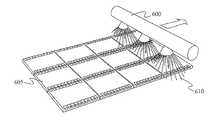
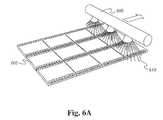
- FIG. 6Aillustrates metallic coating to singulated semiconductor packages via a spraying technique in some embodiments of the present invention.
- FIG. 6Billustrates metallic coating to singulated semiconductor packages via a dipping technique in some embodiments of the present invention.
- FIG. 7illustrates a treated singulated semiconductor package in some embodiments of the present invention.
- Embodiments of the present inventionare directed to a metallic solderability preservation (MSP) coating on metallic contacts of semiconductor package to prevent formulation of oxides.
- MSPmetallic solderability preservation
- Singulated semiconductor packagescan have unexpected material or contaminants, including fingerprints and oxides, on exposed metal areas of semiconductor connectors, including top surfaces and sidewalls. For example, oxidation typically occurs on exposed copper areas of these connectors when the semiconductor packages are not stored in appropriate environments. Copper oxides prevent the metal from soldering well.
- An anti-tarnish solution of the present inventionis used to coat the metal connectors during sawing, after sawing, or both of a semiconductor array to preserve metallic solderability.
- the anti-tarnish solutionin some embodiments is a metallic solution, such as tin, silver, gold, nickel-gold, or any suitable solution. Coating the exposed copper areas with an anti-tarnish solution protects the exposed copper from oxidation. Such coating advantageously allows the semiconductor packages to not need be assembled (e.g., soldered to printed circuit boards) immediately after fabrication.
- singulated semiconductor packagescan be protected from oxidation during or after a sawing process of a semiconductor array, regardless whether the semiconductor array has been previously electroplated. If a singulated semiconductor package is assembled some time after the sawing process, then it is likely that the singulated semiconductor package has been exposed to contaminants, especially if the singulated semiconductor package had not been stored properly. As such, additional measures are taken to ensure that the connectors are free from debris before the preservation of metallic solderability. If the singulated semiconductor package is assembled immediately after the sawing process, then additional measures need not be taken since the singulated semiconductor package has not been exposed to contaminants. Each of the scenarios of metallic solderability preservation is explored in detail below.
- an anti-tarnish solutionis coated on exposed metal areas of connectors after a singulated semiconductor package has been exposed to contaminants, such as oxides.
- contaminantssuch as oxides.
- Exposed metal areas of the connectorsinclude at least sidewalls of the connectors. Top surfaces of the connectors are also exposed if the semiconductor array had not been previously electroplated.
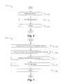
- FIG. 3illustrates an exemplary method 300 of protecting a singulated semiconductor package in one embodiment of the present invention.
- the processstarts at Step 305 with a first cleaning of the semiconductor package using a cleaner agent.
- the cleaner agenthelps reduce surface tension of unexpected material on the semiconductor package.
- the semiconductor packageis immersed in the cleaner agent for five minutes at a temperature of 50° C.
- the cleaner agentis acid, which acts as a detergency and emulsification to effectively remove contaminants, such as oxides and fingerprints.
- a first deionized (DI) water rinseis performed.
- the DI wateris used to rinse the semiconductor package to remove contaminants and the cleaner agent.
- a second cleaning stepis performed.
- the second cleaning stepis micro-etching.
- micro-etchingcreates a uniform topography on the surfaces of the metal connectors.
- Various chemical bathscan be used for micro-etching the connectors, such as hydrogen peroxide, sulphuric acid, sodium persulfate, or any suitable chemical.
- the semiconductor packageis immersed in the chemical bath for about 60 seconds at a temperature of 40° C.
- a second DI water rinseis performed.
- the second DI water rinseensures that exposed surfaces of the metal connectors are clean and are ready for treatment and protection.
- a predipis performed to activate the surfaces of the metal connectors.
- the process time of removing the remaining oxides and/or contaminants and wetting the surfacesis performed for 30 seconds at a temperature of 30° C.
- the “wet” surfacespromote a homogeneous metallic surface finishing.
- the predip solutionis an organic aqueous dispersion that has an efficient anti-tarnishing effect.
- a metallic coatingis applied using an anti-tarnish solution.
- the anti-tarnish solutionin some embodiments is a metallic solution, such as tin, silver, gold, nickel-gold, or any suitable solution.
- the metallic coatingcan be applied in either a high or low temperature for four to twelve minutes via a dipping method or a spraying method.
- the metallic film thicknessat a relatively low temperature of 45-52° C., is about 0.35 micron.
- the metallic film thicknessis about 1 micron.
- the metallic coatingcan be applied to singulated semiconductor packages 605 via spraying the singulated semiconductor packages 605 using the anti-tarnish solution 610 , as illustrated in FIG. 6A , or via dipping the singulated semiconductor packages 605 in the anti-tarnish solution 610 , as illustrated in FIG. 6B .
- the MSP spraying and the MSP dipping, as illustrated,are electrodeless plating techniques. Other electrodeless plating techniques to apply the metallic coating on the semiconductor package are contemplated.
- the singulated semiconductor packages 605are shown in FIGS. 6A-6B as having been through electroplating (e.g., top surfaces of connectors are plated), the methods of protecting a singulated semiconductor package described in FIGS. 3-5 also apply to semiconductor arrays that have not been electroplated (e.g., top surfaces of connectors are not plated), in which both top surfaces and sidewalls are coated at the same time via the MSP process.
- metallic coating on the top surfaces of connectors by electroplatinghas a thickness of about 10 microns, while metallic coating on sidewalls of connectors by MSP has a thickness of 1 micron.
- Metal whiskeringis the spontaneous growth of filiform hairs from a metallic surface. Whiskers cause short circuits and arcing in electrical circuits. If the semiconductor array had been previously electroplated with tin, then tin whiskering may occur. If metallic ion is tin deposit, then tin whiskering is a concerned element. Tin whiskers act like miniature antennas, affecting circuit impedance. Tin whiskers can reduce the conductivity of tin plating. Using a silver (Ag) derivative as an additive in a tin bath helps prevent whisker growth by creating an Ag film on the clean exposed surfaces. The Ag film advantageously decreases both stress formation and velocity of intermetallic layer build up. By the way, whisker growth is not issue for silver, gold, nickle-gold coating.
- embodiments of the present inventioncan be applied to semiconductor packages that have been previously coated with, for example, tin.
- the metallic solution of the present inventionwould also be used as a “filler.” Since the metallic solution can be used as a filler, costs can be minimized because a thinner film of the metallic solution can be applied rather than a thicker film on the surfaces.
- a separate rinseis not required between the Step 330 and the Step 325 because the predip solution does not contain additives.
- the predip solution and the metallic coatinguse the same components.
- a separate rinseis able to be performed between the Step 330 and the Step 325 .
- a third DI water rinseis performed.
- the third DI water rinsecleans excess chemicals and any ionic contaminants before the metallic coating is protected with a postdip solution.
- the DI water used at the Step 335is hot.
- a postdipis performed to prevent oxidation reaction on the metal coating by using an acid or alkaline base.
- the postdipis performed for treatments of both spraying and dipping.
- a fourth DI water rinseis performed.
- the DI water used at the Step 345is hot. In other embodiments, the DI water used at the Step 345 is at room temperature.
- the semiconductor packageis placed in a dryer.
- the dryeris an oven.
- the process 300terminates after the Step 350 .
- the semiconductor packagecan be soldered to a printed circuit board since the connectors have been protected or preserved, which advantageously prevents metal oxidation.
- an anti-tarnish solutionis coated on exposed metal areas of connectors of a singulated semiconductor package immediately after sawing a semiconductor array but before the singulated semiconductor package has been exposed to contaminants. Since the semiconductor package has not been exposed to contaminants during fabrication, cleaning the semiconductor package prior to treatment is therefore not necessary. Such cleaning is to remove possible contaminants.
- FIG. 4illustrates another exemplary method 400 of protecting the singulated semiconductor package in one embodiment of the present invention.
- the processstarts at a Step 405 by applying a metallic coating to the recently singulated semiconductor package using an anti-tarnish solution. Since the Step 405 is similar to the Step 330 discussed above, the Step 405 is not detailed here.
- a first DI water rinseis performed.
- the first DI water rinsecleans excess chemicals and any ionic contaminants.
- the Step 410is similar to the Step 335 .
- a post dip and a second DI water rinseare performed after the first DI water rinse. Although these steps are not illustrated, they are similar to the Steps 340 and 345 described above.
- the semiconductor packageis placed in a dryer.
- the dryeris an oven.
- the process 400terminates after the Step 415 .
- the semiconductor packagecan be soldered to a printed circuit board since the connectors have been protected or preserved, which advantageously prevents metal oxidation.
- Scenario 3Preservation During Sawing
- singulated semiconductor packagescan be protected from oxidation during a sawing process. Since the semiconductor packages would not have been exposed to contaminants during fabrication, cleaning the semiconductor packages prior to treatment is therefore not necessary. Such cleaning is to remove possible contaminants.
- FIG. 5illustrates yet another exemplary method 500 of protecting singulated semiconductor packages in one embodiment of the present invention.
- the processstarts at a Step 505 by loading the semiconductor array that needs to be diced in a singulation saw machine.
- an anti-tarnish solutionsuch as the ones discussed above, is applied to a cutting fluid to form a mixture.
- the cutting fluidis typically used to cool the blade of the singulation saw machine during sawing.
- the Step 505 and the Step 510are interchangeable or can be performed simultaneously.
- the mixtureis sprayed during the sawing process of the semiconductor array.
- the sawing processdices the semiconductor array into a plurality of singulated semiconductor packages.
- Each singulated semiconductor packageis thereby treated with the anti-tarnish solution.
- each singulated semiconductor packageis coated with a layer of metal, such as tin, silver, gold, nickel-gold, or any suitable solution.
- a first DI water rinseis performed.
- the first DI water rinsecleans excess chemicals and any ionic contaminants.
- the DI water used at the Step 520is hot. After preserving the metallic solderability, the semiconductor packages can be soldered to printed circuit boards.
- a post dip and a second DI water rinseare performed after the first DI water rinse. Although these steps are not illustrated, they are similar to the Steps 340 and 345 described above.
- the singulated semiconductor packagesare placed in a dryer.
- the dryeris an oven.
- the process 500terminates after the Step 525 .
- the semiconductor packagecan be soldered to a printed circuit board since the connectors have been protected or preserved, which advantageously prevents metal oxidation.
- MSPcan be applied in other scenarios to prevent contaminations, such oxides, on metal parts by coating the metal parts with an anti-tarnish solution.
- Embodiments of the present inventionadvantageously improves the quality of package soldering to printed circuit boards since contaminants are removed prior to soldering. Further, each of the above described methods advantageously prevents oxidation on the metal conductors of a semiconductor packages.
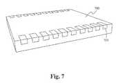
- FIG. 7illustrates a treated singulated semiconductor package 700 in some embodiments of the present invention. It is possible to distinguish between a semiconductor package with and a semiconductor package without MSP. Particularly, a semiconductor package without MSP has connectors that are copperish in color, specifically at least the sidewalls of the connectors, as illustrated in FIG. 2A . In contrast, a semiconductor package with MSP has connectors that are entirely metallically coated. As illustrated in FIG. 7 , top surfaces and sidewalls of the connectors 705 have the same metallic color. However, the colors will be different if two types of metal are used, for example, tin for the top surfaces and gold for the side walls.
- the metallic coating in some embodimentsis a dense metal grain deposit with large and polygonized crystal structures that preserve metallic solderability.
- the metallic coatingcan be of tin, silver, gold, nickel-gold, or any suitable metallic coating.
- Metallic solderability preservationprotects the connectors of the semiconductor package from moisture, thereby preventing metal oxidation.
- Metallic solderability preservationallows a full semiconductor array to be diced prior to shipping.
Landscapes
- Engineering & Computer Science (AREA)
- Microelectronics & Electronic Packaging (AREA)
- Computer Hardware Design (AREA)
- Power Engineering (AREA)
- Physics & Mathematics (AREA)
- Condensed Matter Physics & Semiconductors (AREA)
- General Physics & Mathematics (AREA)
- Manufacturing & Machinery (AREA)
- Preventing Corrosion Or Incrustation Of Metals (AREA)
- Lead Frames For Integrated Circuits (AREA)
- Encapsulation Of And Coatings For Semiconductor Or Solid State Devices (AREA)
Abstract
Description
- This application claims benefit of priority under 35 U.S.C. section 119(e) of the co-pending U.S. Provisional Patent Application Ser. No. 61/210,125 filed Mar. 12, 2009, entitled “Metallic Solderability Preservation (MSP) Coating on Metal Part of Semiconductor Package to Prevent Oxide,” which is hereby incorporated by reference in its entirety.
- The present invention is related to the field of semiconductor device manufacturing. More specifically, the present invention relates to metallic solderability preservation coating on metal part of semiconductor package to prevent oxide.
- A semiconductor device array contains individual integrated circuits or semiconductor packages.
Connectors 105 of the semiconductor packages are exposed at the top of thesemiconductor array 100, as illustrated inFIG. 1A . Theconnectors 105 are typically made of copper. To prevent oxidation on the copper surface, theconnectors 105 are plated with a lead finished material, such as matte tin (Sn), using electroplating. As a result, the top surfaces of theconnectors 105′ are thereafter tin plated, as illustrated inFIG. 1B . - Singulation is a process of separating each semiconductor package from a molded sheet. Dicing or sawing is a process that singulates the
semiconductor array 100′ into individual or singulated semiconductor packages. Conventionally, theelectroplated semiconductor array 100′ is diced into singulated semiconductor packages to be shipped to customers for assembly onto printed circuit boards.FIG. 1C illustrates asaw 115 dicing thesemiconductor array 100′. Thesaw 115 typically follows asaw path 110 across theplated connectors 105′, resulting in connectors on peripheral edges of the singulated semiconductor packages. FIG. 2A illustrates a singulatedsemiconductor package 200 having a plurality of connectors205 on the peripheral edges. Although tops of theconnectors 205aare tin plated, sidewalls of theconnectors 205bare exposed (e.g., without tin plating), because the dicing occurred after thesemiconductor array 100 was electroplated with the lead finished material. If the singulatedsemiconductor package 200 is stored in inappropriate environments and/or conditions (e.g., moisture in the air, acids, bases, salts, oils, aggressive metal polished, and other solid and liquid chemicals) after singulation, then the exposedsurfaces 205bbecome sites forpotential corrosion 210 such as copper oxide, as illustrated inFIG. 2B . This aging process is known as oxidation. The exposedsurfaces 205b,usually deposited with pollutant layers of oxide and othernonmetallic compound 210, often interfere with or inhibit solder wettability. The resulting oxide layer reduces solderability becausecontamination 210 prevents the metal from soldering well. The rate of oxidation can increase with an increase in temperature or humidity. Solder problems are a common cause for device failures.- A perfectly clean surface is required for assembly of singulated
semiconductor packages 200 onto printed circuit boards. Since metal oxides form a barrier that prevents molten solder from forming a true metallurgical bond, the metal oxides must be removed prior to soldering or must be avoided in the first place. - The present invention addresses at least these limitations in the prior art.
- A first aspect of the present invention is for a method of preventing contaminants from forming on metal surfaces of semiconductor package connectors. The method includes performing a first cleaning of a semiconductor package using a cleaner agent, thereby reducing surface tension of unexpected material. Performing the first cleaning includes immersing the semiconductor package in the cleaner agent. In some embodiments, the semiconductor package is immersed in the cleaner agent for five minutes at 50° C. In some embodiments, the cleaner agent is acid. The method further includes performing a first DI water rinsing of the semiconductor package, thereby removing the undesired material and the cleaner agent. The method further includes performing a second cleaning of the semiconductor package. In some embodiments, the second cleaning is micro-etching, wherein the micro-etching creates a uniform topography on the surfaces of the metal connectors. In some embodiments, the second cleaning includes immersing the semiconductor package in a chemical bath. The chemical bath is hydrogen peroxide, sulphuric acid, sodium persulfate, or any suitable chemical bath. In some embodiments, the semiconductor package is immersed in the chemical bath for about 60 seconds at 40° C. The method further includes performing a second DI water rinsing of the semiconductor package, thereby ensuring exposed surfaces of metal connectors are clean and ready for treatment. The semiconductor package is predipped, thereby activating the surfaces. In some embodiments, the predipping includes removing oxides and wetting the clean surfaces for 30 seconds at 30° C. in a predip solution, wherein the wet surfaces promotes a homogeneous metallic surface finishing. The predip solution is preferably an organic aqueous dispersion that has an efficient anti-tarnishing effect. The method further includes treating the semiconductor package with an anti-tarnish solution. In some embodiments, the treating step includes spraying the semiconductor package with the anti-tarnish solution. Alternatively, the treating step includes dipping the semiconductor package with the anti-tarnish solution. The anti-tarnish solution is preferably a metallic solution. In some embodiments, the anti-tarnish solution is applied to the semiconductor package at 45-52° C. or at 63-68° C. The anti-tarnish solution is applied to the semiconductor package for four to twelve minutes. The method further includes performing a third DI water rinsing of the semiconductor package, thereby cleaning excess chemical and ionic contaminants, and postdipping the semiconductor package, thereby protecting a metallic coating. The metallic coating prevents oxidation. A postdip solution is one of acid or alkaline base. The method further includes preforming a fourth DI water rinsing of the semiconductor package, and drying the semiconductor package. In some embodiments, the method further includes soldering the semiconductor package to a printed circuit board.
- A second aspect of the present invention is for a method of preventing contaminants from forming on metal surfaces of semiconductor package connector. The method includes treating a semiconductor package with an anti-tarnish solution. In some embodiments, the treating step includes spraying the semiconductor package with the anti-tarnish solution. Alternatively, the treating step includes dipping the semiconductor package with the anti-tarnish solution. The anti-tarnish solution is preferably a metallic solution. In some embodiments, the anti-tarnish solution is applied to the semiconductor package at 45-52° C. or at 63-68° C. The anti-tarnish solution is applied to the semiconductor package for four to twelve minutes. The method further includes performing a first DI water rinsing of the semiconductor package, thereby cleaning excess chemical and ionic contaminants, and drying the semiconductor package. In some embodiments, the method further includes soldering the semiconductor package to a printed circuit board.
- A third aspect of the present invention is also for a method of preventing contaminants from forming on metal surfaces of semiconductor package connector. The method includes creating a mixture for use during singulation, and spraying a semiconductor array with the mixture during singulation, thereby treating a plurality of semiconductor packages. This creating step includes adding an anti-tarnish solution to a cutting fluid. The anti-tarnish solution is a metallic solution. In some embodiments, the anti-tarnish solution is applied to the plurality of semiconductor packages at 45-52° C. or at 63-68° C. The anti-tarnish solution is applied to the plurality of semiconductor packages for four to twelve minutes. The method further includes performing a first DI water rinsing of at least one semiconductor package, and drying the at least one semiconductor package. In some embodiments, the method further includes soldering the at least one semiconductor package to a printed circuit board.
- A fourth aspect of the present invention is for a method of preserving metallic solderability of a semiconductor package. The method includes coating connectors with a metallic solution, wherein the coating occurs during or after sawing a semiconductor array, wherein the sawing creates a plurality of semiconductor packages, wherein the metallic solution is configured to prevent metal oxidation. The metallic solution is an anti-tarnish solution. The metallic solution is tin, silver, gold, nickel-gold, or any suitable metallic solution. In some embodiments, the coating is applied via dipping the semiconductor package in the metallic solution or by spraying the semiconductor package with the metallic solution when the coating occurs after sawing the semiconductor array. In some embodiments, the coating is applied via spraying when the coating occurs during sawing of the semiconductor array. In some embodiments, the coating occurs at 45-52° C. or at 63-68° C. The coating is applied for four to twelve minutes. In some embodiments, the method includes, before the coating, performing at least one cleaning and at least one rinsing of the semiconductor package when the semiconductor package is exposed to contaminants. In some embodiments, the method further includes soldering the semiconductor package to a printed circuit board.
- A fifth aspect of the present invention is for a metallic solderability preservation method. A semiconductor array is loaded into a singulation machine. The semiconductor array includes a plurality of semiconductor packages. The semiconductor packages are treated with an anti-tarnish solution, thereby plating all exposed surfaces of semiconductor connectors. In some embodiments, the loading step includes mixing the anti-tarnish solution with a cutting fluid, such that the treating occurs when the mixture is sprayed on the semiconductor array during dicing. Alternatively, the semiconductor packages are sprayed with the anti-tarnish solution after singulation. Alternatively, the semiconductor packages are dipped into the anti-tarnish solution after singulation. In some embodiments, the anti-tarnish solution is a metallic solution. The metallic solution is one of tin, silver, gold, and nickel-gold. In some embodiments, the anti-metallic solution is applied at 45-52° C. or at 63-68° C. The anti-metallic solution is applied for four to twelve minutes. In some embodiments, the method further includes soldering the semiconductor package to a printed circuit board.
- The novel features of the invention are set forth in the appended claims. However, for purpose of explanation, several embodiments of the invention are set forth in the following figures.
FIG. 1A illustrates an exemplary semiconductor array.FIG. 1B illustrates the semiconductor array with connectors coated with tin.FIG. 1C illustrates the semiconductor array being diced with a saw.FIG. 2A illustrates a singulated semiconductor package having a plurality of connectors on peripheral edges.FIG. 2B illustrates the plurality of connectors with contaminants.FIG. 3 illustrates an exemplary method of protecting a singulated semiconductor package in one embodiment of the present invention.FIG. 4 illustrates another exemplary method of protecting a singulated semiconductor package in one embodiment of the present invention.FIG. 5 illustrates yet another exemplary method of protecting a singulated semiconductor package in one embodiment of the present invention.FIG. 6A illustrates metallic coating to singulated semiconductor packages via a spraying technique in some embodiments of the present invention.FIG. 6B illustrates metallic coating to singulated semiconductor packages via a dipping technique in some embodiments of the present invention.FIG. 7 illustrates a treated singulated semiconductor package in some embodiments of the present invention.- In the following description, numerous details are set forth for purposes of explanation.
- However, one of ordinary skill in the art will realize that the invention can be practiced without the use of these specific details. Thus, the present invention is not intended to be limited to the embodiments shown but is to be accorded the widest scope consistent with the principles and features described herein or with equivalent alternatives.
- Reference will now be made in detail to implementations of the present invention as illustrated in the accompanying drawings. The same reference indicators will be used throughout the drawings and the following detailed description to refer to the same or like parts.
- Embodiments of the present invention are directed to a metallic solderability preservation (MSP) coating on metallic contacts of semiconductor package to prevent formulation of oxides. Singulated semiconductor packages can have unexpected material or contaminants, including fingerprints and oxides, on exposed metal areas of semiconductor connectors, including top surfaces and sidewalls. For example, oxidation typically occurs on exposed copper areas of these connectors when the semiconductor packages are not stored in appropriate environments. Copper oxides prevent the metal from soldering well.
- An anti-tarnish solution of the present invention is used to coat the metal connectors during sawing, after sawing, or both of a semiconductor array to preserve metallic solderability. The anti-tarnish solution in some embodiments is a metallic solution, such as tin, silver, gold, nickel-gold, or any suitable solution. Coating the exposed copper areas with an anti-tarnish solution protects the exposed copper from oxidation. Such coating advantageously allows the semiconductor packages to not need be assembled (e.g., soldered to printed circuit boards) immediately after fabrication.
- As discussed above, singulated semiconductor packages can be protected from oxidation during or after a sawing process of a semiconductor array, regardless whether the semiconductor array has been previously electroplated. If a singulated semiconductor package is assembled some time after the sawing process, then it is likely that the singulated semiconductor package has been exposed to contaminants, especially if the singulated semiconductor package had not been stored properly. As such, additional measures are taken to ensure that the connectors are free from debris before the preservation of metallic solderability. If the singulated semiconductor package is assembled immediately after the sawing process, then additional measures need not be taken since the singulated semiconductor package has not been exposed to contaminants. Each of the scenarios of metallic solderability preservation is explored in detail below.
- Scenario 1: Preservation after Sawing and Exposure to Contaminants
- In some embodiments, an anti-tarnish solution is coated on exposed metal areas of connectors after a singulated semiconductor package has been exposed to contaminants, such as oxides. As discussed above, oxidation occurs when the semiconductor package is not stored in an appropriate environment after fabrication. Exposed metal areas of the connectors include at least sidewalls of the connectors. Top surfaces of the connectors are also exposed if the semiconductor array had not been previously electroplated.
- Assuming that the semiconductor package has been singulated from a semiconductor array and has not yet been assembled (e.g., soldered to a printed circuit board),
FIG. 3 illustrates anexemplary method 300 of protecting a singulated semiconductor package in one embodiment of the present invention. The process starts atStep 305 with a first cleaning of the semiconductor package using a cleaner agent. The cleaner agent helps reduce surface tension of unexpected material on the semiconductor package. In some embodiments, the semiconductor package is immersed in the cleaner agent for five minutes at a temperature of 50° C. In some embodiments, the cleaner agent is acid, which acts as a detergency and emulsification to effectively remove contaminants, such as oxides and fingerprints. - At a
Step 310, a first deionized (DI) water rinse is performed. The DI water is used to rinse the semiconductor package to remove contaminants and the cleaner agent. - At a
Step 315, a second cleaning step is performed. In some embodiments, the second cleaning step is micro-etching. Preferably, micro-etching creates a uniform topography on the surfaces of the metal connectors. Various chemical baths can be used for micro-etching the connectors, such as hydrogen peroxide, sulphuric acid, sodium persulfate, or any suitable chemical. In some embodiments, the semiconductor package is immersed in the chemical bath for about 60 seconds at a temperature of 40° C. - At a
Step 320, a second DI water rinse is performed. The second DI water rinse ensures that exposed surfaces of the metal connectors are clean and are ready for treatment and protection. - However, before treatment and protection, at a Step325, a predip is performed to activate the surfaces of the metal connectors. In some embodiments, the process time of removing the remaining oxides and/or contaminants and wetting the surfaces is performed for 30 seconds at a temperature of 30° C. The “wet” surfaces promote a homogeneous metallic surface finishing. In some embodiments, the predip solution is an organic aqueous dispersion that has an efficient anti-tarnishing effect.
- At a
Step 330, a metallic coating is applied using an anti-tarnish solution. The anti-tarnish solution in some embodiments is a metallic solution, such as tin, silver, gold, nickel-gold, or any suitable solution. Depending on the desired thickness of the metallic film, the metallic coating can be applied in either a high or low temperature for four to twelve minutes via a dipping method or a spraying method. In some embodiments, at a relatively low temperature of 45-52° C., the metallic film thickness is about 0.35 micron. In some embodiments, at a relatively high temperature of 63-68° C., the metallic film thickness is about 1 micron. - The metallic coating can be applied to
singulated semiconductor packages 605 via spraying thesingulated semiconductor packages 605 using theanti-tarnish solution 610, as illustrated inFIG. 6A , or via dipping thesingulated semiconductor packages 605 in theanti-tarnish solution 610, as illustrated inFIG. 6B . The MSP spraying and the MSP dipping, as illustrated, are electrodeless plating techniques. Other electrodeless plating techniques to apply the metallic coating on the semiconductor package are contemplated. - Although the
singulated semiconductor packages 605 are shown inFIGS. 6A-6B as having been through electroplating (e.g., top surfaces of connectors are plated), the methods of protecting a singulated semiconductor package described inFIGS. 3-5 also apply to semiconductor arrays that have not been electroplated (e.g., top surfaces of connectors are not plated), in which both top surfaces and sidewalls are coated at the same time via the MSP process. In some embodiments, metallic coating on the top surfaces of connectors by electroplating has a thickness of about 10 microns, while metallic coating on sidewalls of connectors by MSP has a thickness of 1 micron. - Metal whiskering is the spontaneous growth of filiform hairs from a metallic surface. Whiskers cause short circuits and arcing in electrical circuits. If the semiconductor array had been previously electroplated with tin, then tin whiskering may occur. If metallic ion is tin deposit, then tin whiskering is a concerned element. Tin whiskers act like miniature antennas, affecting circuit impedance. Tin whiskers can reduce the conductivity of tin plating. Using a silver (Ag) derivative as an additive in a tin bath helps prevent whisker growth by creating an Ag film on the clean exposed surfaces. The Ag film advantageously decreases both stress formation and velocity of intermetallic layer build up. By the way, whisker growth is not issue for silver, gold, nickle-gold coating.
- It should be understood that embodiments of the present invention can be applied to semiconductor packages that have been previously coated with, for example, tin. In such a case, the metallic solution of the present invention would also be used as a “filler.” Since the metallic solution can be used as a filler, costs can be minimized because a thinner film of the metallic solution can be applied rather than a thicker film on the surfaces.
- In some embodiments, a separate rinse is not required between the
Step 330 and the Step325 because the predip solution does not contain additives. In some embodiments, the predip solution and the metallic coating use the same components. In other embodiments, a separate rinse is able to be performed between theStep 330 and the Step325. - At a
Step 335, a third DI water rinse is performed. The third DI water rinse cleans excess chemicals and any ionic contaminants before the metallic coating is protected with a postdip solution. In some embodiments, the DI water used at theStep 335 is hot. - At a
Step 340, a postdip is performed to prevent oxidation reaction on the metal coating by using an acid or alkaline base. The postdip is performed for treatments of both spraying and dipping. - At a
Step 345, a fourth DI water rinse is performed. In some embodiments, the DI water used at theStep 345 is hot. In other embodiments, the DI water used at theStep 345 is at room temperature. - At a
Step 350, the semiconductor package is placed in a dryer. In some embodiments, the dryer is an oven. Theprocess 300 terminates after theStep 350. At any time after preserving the metallic solderability, the semiconductor package can be soldered to a printed circuit board since the connectors have been protected or preserved, which advantageously prevents metal oxidation. - Scenario 2: Preservation Immediately after Sawing but Before Exposure to Contaminants
- In some embodiments, an anti-tarnish solution is coated on exposed metal areas of connectors of a singulated semiconductor package immediately after sawing a semiconductor array but before the singulated semiconductor package has been exposed to contaminants. Since the semiconductor package has not been exposed to contaminants during fabrication, cleaning the semiconductor package prior to treatment is therefore not necessary. Such cleaning is to remove possible contaminants.
- Assuming that the semiconductor package has been singulated from a semiconductor array and has not yet been assembled (e.g. soldered to a printed circuit board),
FIG. 4 illustrates anotherexemplary method 400 of protecting the singulated semiconductor package in one embodiment of the present invention. The process starts at aStep 405 by applying a metallic coating to the recently singulated semiconductor package using an anti-tarnish solution. Since theStep 405 is similar to theStep 330 discussed above, theStep 405 is not detailed here. - At a
Step 410, a first DI water rinse is performed. The first DI water rinse cleans excess chemicals and any ionic contaminants. TheStep 410 is similar to theStep 335. - In some embodiments, a post dip and a second DI water rinse are performed after the first DI water rinse. Although these steps are not illustrated, they are similar to the
Steps - At a
Step 415, the semiconductor package is placed in a dryer. In some embodiments, the dryer is an oven. Theprocess 400 terminates after theStep 415. At any time after preserving the metallic solderability, the semiconductor package can be soldered to a printed circuit board since the connectors have been protected or preserved, which advantageously prevents metal oxidation. - In some embodiments, singulated semiconductor packages can be protected from oxidation during a sawing process. Since the semiconductor packages would not have been exposed to contaminants during fabrication, cleaning the semiconductor packages prior to treatment is therefore not necessary. Such cleaning is to remove possible contaminants.
- Assuming that the semiconductor packages have not yet been singulated from a semiconductor array,
FIG. 5 illustrates yet anotherexemplary method 500 of protecting singulated semiconductor packages in one embodiment of the present invention. The process starts at aStep 505 by loading the semiconductor array that needs to be diced in a singulation saw machine. - At a
Step 510, an anti-tarnish solution, such as the ones discussed above, is applied to a cutting fluid to form a mixture. The cutting fluid is typically used to cool the blade of the singulation saw machine during sawing. In some embodiments, theStep 505 and theStep 510 are interchangeable or can be performed simultaneously. - At a
Step 515, the mixture is sprayed during the sawing process of the semiconductor array. The sawing process dices the semiconductor array into a plurality of singulated semiconductor packages. Each singulated semiconductor package is thereby treated with the anti-tarnish solution. In other words, each singulated semiconductor package is coated with a layer of metal, such as tin, silver, gold, nickel-gold, or any suitable solution. - At a
Step 520, a first DI water rinse is performed. The first DI water rinse cleans excess chemicals and any ionic contaminants. In some embodiments, the DI water used at theStep 520 is hot. After preserving the metallic solderability, the semiconductor packages can be soldered to printed circuit boards. - In some embodiments, a post dip and a second DI water rinse are performed after the first DI water rinse. Although these steps are not illustrated, they are similar to the
Steps - At a
Step 525, the singulated semiconductor packages are placed in a dryer. In some embodiments, the dryer is an oven. Theprocess 500 terminates after theStep 525. At any time after preserving the metallic solderability, the semiconductor package can be soldered to a printed circuit board since the connectors have been protected or preserved, which advantageously prevents metal oxidation. - It should be understood that MSP can be applied in other scenarios to prevent contaminations, such oxides, on metal parts by coating the metal parts with an anti-tarnish solution.
- Singulated Semiconductor Packages with MSP Coating
- Embodiments of the present invention advantageously improves the quality of package soldering to printed circuit boards since contaminants are removed prior to soldering. Further, each of the above described methods advantageously prevents oxidation on the metal conductors of a semiconductor packages.
FIG. 7 illustrates a treatedsingulated semiconductor package 700 in some embodiments of the present invention. It is possible to distinguish between a semiconductor package with and a semiconductor package without MSP. Particularly, a semiconductor package without MSP has connectors that are copperish in color, specifically at least the sidewalls of the connectors, as illustrated inFIG. 2A . In contrast, a semiconductor package with MSP has connectors that are entirely metallically coated. As illustrated inFIG. 7 , top surfaces and sidewalls of theconnectors 705 have the same metallic color. However, the colors will be different if two types of metal are used, for example, tin for the top surfaces and gold for the side walls.- The metallic coating in some embodiments is a dense metal grain deposit with large and polygonized crystal structures that preserve metallic solderability. The metallic coating can be of tin, silver, gold, nickel-gold, or any suitable metallic coating. Metallic solderability preservation protects the connectors of the semiconductor package from moisture, thereby preventing metal oxidation. Metallic solderability preservation allows a full semiconductor array to be diced prior to shipping.
- While the invention has been described with reference to numerous specific details, one of ordinary skill in the art will recognize that the invention can be embodied in other specific forms without departing from the spirit of the invention. Thus, one of ordinary skill in the art will understand that the invention is not to be limited by the foregoing illustrative details, but rather is to be defined by the appended claims.
Claims (45)
Priority Applications (1)
| Application Number | Priority Date | Filing Date | Title |
|---|---|---|---|
| US13/156,257US8431443B2 (en) | 2009-03-12 | 2011-06-08 | Metallic solderability preservation coating on metal part of semiconductor package to prevent oxide |
Applications Claiming Priority (3)
| Application Number | Priority Date | Filing Date | Title |
|---|---|---|---|
| US21012509P | 2009-03-12 | 2009-03-12 | |
| US12/579,574US8367476B2 (en) | 2009-03-12 | 2009-10-15 | Metallic solderability preservation coating on metal part of semiconductor package to prevent oxide |
| US13/156,257US8431443B2 (en) | 2009-03-12 | 2011-06-08 | Metallic solderability preservation coating on metal part of semiconductor package to prevent oxide |
Related Parent Applications (1)
| Application Number | Title | Priority Date | Filing Date |
|---|---|---|---|
| US12/579,574DivisionUS8367476B2 (en) | 2009-03-12 | 2009-10-15 | Metallic solderability preservation coating on metal part of semiconductor package to prevent oxide |
Publications (2)
| Publication Number | Publication Date |
|---|---|
| US20110232693A1true US20110232693A1 (en) | 2011-09-29 |
| US8431443B2 US8431443B2 (en) | 2013-04-30 |
Family
ID=42730005
Family Applications (3)
| Application Number | Title | Priority Date | Filing Date |
|---|---|---|---|
| US12/579,600Active2030-06-22US8569877B2 (en) | 2009-03-12 | 2009-10-15 | Metallic solderability preservation coating on metal part of semiconductor package to prevent oxide |
| US12/579,574Active2029-12-09US8367476B2 (en) | 2009-03-12 | 2009-10-15 | Metallic solderability preservation coating on metal part of semiconductor package to prevent oxide |
| US13/156,257Active2029-11-01US8431443B2 (en) | 2009-03-12 | 2011-06-08 | Metallic solderability preservation coating on metal part of semiconductor package to prevent oxide |
Family Applications Before (2)
| Application Number | Title | Priority Date | Filing Date |
|---|---|---|---|
| US12/579,600Active2030-06-22US8569877B2 (en) | 2009-03-12 | 2009-10-15 | Metallic solderability preservation coating on metal part of semiconductor package to prevent oxide |
| US12/579,574Active2029-12-09US8367476B2 (en) | 2009-03-12 | 2009-10-15 | Metallic solderability preservation coating on metal part of semiconductor package to prevent oxide |
Country Status (2)
| Country | Link |
|---|---|
| US (3) | US8569877B2 (en) |
| CN (3) | CN101840846B (en) |
Families Citing this family (7)
| Publication number | Priority date | Publication date | Assignee | Title |
|---|---|---|---|---|
| US9496195B2 (en) | 2012-10-02 | 2016-11-15 | STATS ChipPAC Pte. Ltd. | Semiconductor device and method of depositing encapsulant along sides and surface edge of semiconductor die in embedded WLCSP |
| US9620413B2 (en) | 2012-10-02 | 2017-04-11 | STATS ChipPAC Pte. Ltd. | Semiconductor device and method of using a standardized carrier in semiconductor packaging |
| WO2014055630A1 (en) | 2012-10-04 | 2014-04-10 | Fci | Electrical contact including corrosion-resistant coating |
| US9704824B2 (en) | 2013-01-03 | 2017-07-11 | STATS ChipPAC Pte. Ltd. | Semiconductor device and method of forming embedded wafer level chip scale packages |
| US9721862B2 (en) | 2013-01-03 | 2017-08-01 | STATS ChipPAC Pte. Ltd. | Semiconductor device and method of using a standardized carrier to form embedded wafer level chip scale packages |
| US9255451B2 (en)* | 2013-01-29 | 2016-02-09 | Baker Hughes Incorporated | Tube locking mechanism for downhole components |
| US9759017B2 (en) | 2013-01-30 | 2017-09-12 | Baker Hughes Incorporated | Maintaining tension of a transmission line in a tubular |
Citations (91)
| Publication number | Priority date | Publication date | Assignee | Title |
|---|---|---|---|---|
| US361106A (en)* | 1887-04-12 | Envelope gumming and drying apparatus | ||
| US4411719A (en)* | 1980-02-07 | 1983-10-25 | Westinghouse Electric Corp. | Apparatus and method for tape bonding and testing of integrated circuit chips |
| US4501960A (en)* | 1981-06-22 | 1985-02-26 | Motorola, Inc. | Micropackage for identification card |
| US4801561A (en)* | 1984-07-05 | 1989-01-31 | National Semiconductor Corporation | Method for making a pre-testable semiconductor die package |
| US4855672A (en)* | 1987-05-18 | 1989-08-08 | Shreeve Robert W | Method and process for testing the reliability of integrated circuit (IC) chips and novel IC circuitry for accomplishing same |
| US5247248A (en)* | 1991-02-18 | 1993-09-21 | Sharp Kabushiki Kaisha | Burn-in apparatus and method of use thereof |
| US5248075A (en)* | 1992-04-13 | 1993-09-28 | Micron Technology, Inc. | IC pin forming machine with integrated IC testing capability |
| US5396185A (en)* | 1990-08-13 | 1995-03-07 | Kabushiki Kaisha Toshiba | System and carrier for testing semiconductor integrated circuit devices |
| US5397921A (en)* | 1993-09-03 | 1995-03-14 | Advanced Semiconductor Assembly Technology | Tab grid array |
| US5535101A (en)* | 1992-11-03 | 1996-07-09 | Motorola, Inc. | Leadless integrated circuit package |
| US5596231A (en)* | 1991-08-05 | 1997-01-21 | Asat, Limited | High power dissipation plastic encapsulated package for integrated circuit die |
| US6072239A (en)* | 1995-11-08 | 2000-06-06 | Fujitsu Limited | Device having resin package with projections |
| US6111324A (en)* | 1998-02-05 | 2000-08-29 | Asat, Limited | Integrated carrier ring/stiffener and method for manufacturing a flexible integrated circuit package |
| US6229200B1 (en)* | 1998-06-10 | 2001-05-08 | Asat Limited | Saw-singulated leadless plastic chip carrier |
| US6285075B1 (en)* | 1998-11-02 | 2001-09-04 | Asat, Limited | Integrated circuit package with bonding planes on a ceramic ring using an adhesive assembly |
| US6294100B1 (en)* | 1998-06-10 | 2001-09-25 | Asat Ltd | Exposed die leadless plastic chip carrier |
| US6304000B1 (en)* | 1997-04-30 | 2001-10-16 | Dow Corning Toray Silicone Company, Ltd. | Semiconductor device comprising silicone adhesive sheet |
| US6353263B1 (en)* | 1999-04-14 | 2002-03-05 | Sharp Kabushiki Kaisha | Semiconductor device and manufacturing method thereof |
| US6376921B1 (en)* | 1995-11-08 | 2002-04-23 | Fujitsu Limited | Semiconductor device, method for fabricating the semiconductor device, lead frame and method for producing the lead frame |
| US6392427B1 (en)* | 1998-12-21 | 2002-05-21 | Kaitech Engineering, Inc. | Testing electronic devices |
| US6414385B1 (en)* | 1999-11-08 | 2002-07-02 | Siliconware Precisionindustries Co., Ltd. | Quad flat non-lead package of semiconductor |
| US6429048B1 (en)* | 2000-12-05 | 2002-08-06 | Asat Ltd. | Metal foil laminated IC package |
| US6451709B1 (en)* | 1998-09-03 | 2002-09-17 | Micron Technology, Inc. | Methodology of removing misplaced encapsulant for attachment of heat sinks in a chip on board package |
| US6455348B1 (en)* | 1998-03-12 | 2002-09-24 | Matsushita Electric Industrial Co., Ltd. | Lead frame, resin-molded semiconductor device, and method for manufacturing the same |
| US20030003586A1 (en)* | 1998-02-10 | 2003-01-02 | Angros Lee H. | Analytic plate with containment border and method |
| US20030006055A1 (en)* | 2001-07-05 | 2003-01-09 | Walsin Advanced Electronics Ltd | Semiconductor package for fixed surface mounting |
| US6507116B1 (en)* | 1997-04-24 | 2003-01-14 | International Business Machines Corporation | Electronic package and method of forming |
| US20030045032A1 (en)* | 2001-08-31 | 2003-03-06 | Shinko Electric Industries Co., Ltd. | Leadframe, method of manufacturing the same, semiconductor device using the same, and method of manufacturing the device |
| US6545347B2 (en)* | 2001-03-06 | 2003-04-08 | Asat, Limited | Enhanced leadless chip carrier |
| US6545332B2 (en)* | 2001-01-17 | 2003-04-08 | Siliconware Precision Industries Co., Ltd. | Image sensor of a quad flat package |
| US20030071333A1 (en)* | 2001-10-15 | 2003-04-17 | Shinko Electric Industries Co., Ltd. | Leadframe, method of manufacturing the same, and method of manufacturing a semiconductor device using the same |
| US6552423B2 (en)* | 2000-02-18 | 2003-04-22 | Samsung Electronics Co., Ltd. | Higher-density memory card |
| US6552417B2 (en)* | 1993-09-03 | 2003-04-22 | Asat, Limited | Molded plastic package with heat sink and enhanced electrical performance |
| US6566740B2 (en)* | 2000-03-23 | 2003-05-20 | Mitsui High-Tec, Inc. | Lead frame for a semiconductor device and method of manufacturing a semiconductor device |
| US6585905B1 (en)* | 1998-06-10 | 2003-07-01 | Asat Ltd. | Leadless plastic chip carrier with partial etch die attach pad |
| US6586834B1 (en)* | 2002-06-17 | 2003-07-01 | Asat Ltd. | Die-up tape ball grid array package |
| US20030143776A1 (en)* | 2002-01-31 | 2003-07-31 | Serafin Pedron | Method of manufacturing an encapsulated integrated circuit package |
| US20030178719A1 (en)* | 2002-03-22 | 2003-09-25 | Combs Edward G. | Enhanced thermal dissipation integrated circuit package and method of manufacturing enhanced thermal dissipation integrated circuit package |
| US6660626B1 (en)* | 2000-08-22 | 2003-12-09 | Charles W. C. Lin | Semiconductor chip assembly with simultaneously electrolessly plated contact terminal and connection joint |
| US20040014257A1 (en)* | 2002-07-19 | 2004-01-22 | Kim Pyoung Wan | Method for joining lead frames in a package assembly, method for forming a chip stack package, and a chip stack package |
| US6686667B2 (en)* | 2002-04-22 | 2004-02-03 | Scientek Corp. | Image sensor semiconductor package with castellation |
| US6703696B2 (en)* | 2000-09-04 | 2004-03-09 | Dainippon Printing Co., Ltd. | Semiconductor package |
| US20040046237A1 (en)* | 2002-09-05 | 2004-03-11 | Shinko Electric Industries Co., Ltd | Lead frame and method of manufacturing the same |
| US6724071B2 (en)* | 1993-09-03 | 2004-04-20 | Asat, Limited | Molded plastic package with heat sink and enhanced electrical performance |
| US20040080025A1 (en)* | 2002-09-17 | 2004-04-29 | Shinko Electric Industries Co., Ltd. | Lead frame, method of manufacturing the same, and semiconductor device manufactured with the same |
| US6734552B2 (en)* | 2001-07-11 | 2004-05-11 | Asat Limited | Enhanced thermal dissipation integrated circuit package |
| US6734044B1 (en)* | 2002-06-10 | 2004-05-11 | Asat Ltd. | Multiple leadframe laminated IC package |
| US6737755B1 (en)* | 2002-07-19 | 2004-05-18 | Asat, Ltd. | Ball grid array package with improved thermal characteristics |
| US20040110319A1 (en)* | 1994-03-18 | 2004-06-10 | Hitachi Chemical Company, Ltd. | Fabrication process of semiconductor package and semiconductor package |
| US6764880B2 (en)* | 2001-11-15 | 2004-07-20 | Siliconware Precision Industries Co., Ltd. | Semiconductor package and fabricating method thereof |
| US6781242B1 (en)* | 2002-12-02 | 2004-08-24 | Asat, Ltd. | Thin ball grid array package |
| US6841859B1 (en)* | 2002-09-03 | 2005-01-11 | Asat Ltd. | Premolded cavity IC package |
| US6876066B2 (en)* | 2001-08-29 | 2005-04-05 | Micron Technology, Inc. | Packaged microelectronic devices and methods of forming same |
| US20050077613A1 (en)* | 2002-01-31 | 2005-04-14 | Mclellan Neil Robert | Integrated circuit package |
| US6897428B2 (en)* | 2003-07-01 | 2005-05-24 | Matsushita Electric Industrial Co., Ltd. | Solid-state imaging device and method for manufacturing the same |
| US6933176B1 (en)* | 2002-07-19 | 2005-08-23 | Asat Ltd. | Ball grid array package and process for manufacturing same |
| US6933594B2 (en)* | 1998-06-10 | 2005-08-23 | Asat Ltd. | Leadless plastic chip carrier with etch back pad singulation |
| US6940154B2 (en)* | 2002-06-24 | 2005-09-06 | Asat Limited | Integrated circuit package and method of manufacturing the integrated circuit package |
| US6946918B2 (en)* | 2002-01-16 | 2005-09-20 | Oki Electric Industry Co., Ltd. | Differential voltage to current converter having transistors of different sizes |
| US6946324B1 (en)* | 1998-06-10 | 2005-09-20 | Asat Ltd. | Process for fabricating a leadless plastic chip carrier |
| US6969638B2 (en)* | 2003-06-27 | 2005-11-29 | Texas Instruments Incorporated | Low cost substrate for an integrated circuit device with bondpads free of plated gold |
| US6982491B1 (en)* | 2004-01-20 | 2006-01-03 | Asat Ltd. | Sensor semiconductor package and method of manufacturing the same |
| US6984785B1 (en)* | 2003-10-27 | 2006-01-10 | Asat Ltd. | Thermally enhanced cavity-down integrated circuit package |
| US7008825B1 (en)* | 2003-05-27 | 2006-03-07 | Amkor Technology, Inc. | Leadframe strip having enhanced testability |
| US7009286B1 (en)* | 2004-01-15 | 2006-03-07 | Asat Ltd. | Thin leadless plastic chip carrier |
| US7049177B1 (en)* | 2004-01-28 | 2006-05-23 | Asat Ltd. | Leadless plastic chip carrier with standoff contacts and die attach pad |
| US7060535B1 (en)* | 2003-10-29 | 2006-06-13 | Ns Electronics Bangkok (1993) Ltd. | Flat no-lead semiconductor die package including stud terminals |
| US7071545B1 (en)* | 2002-12-20 | 2006-07-04 | Asat Ltd. | Shielded integrated circuit package |
| US7091581B1 (en)* | 2004-06-14 | 2006-08-15 | Asat Limited | Integrated circuit package and process for fabricating the same |
| US20060192295A1 (en)* | 2004-11-17 | 2006-08-31 | Chippac, Inc. | Semiconductor package flip chip interconnect having spacer |
| US7101210B2 (en)* | 2004-11-26 | 2006-09-05 | Hon Hai Precision Ind. Co., Ltd. | LGA socket |
| US20070001278A1 (en)* | 2005-06-30 | 2007-01-04 | Oseob Jeon | Semiconductor die package and method for making the same |
| US7205178B2 (en)* | 2004-03-24 | 2007-04-17 | Freescale Semiconductor, Inc. | Land grid array packaged device and method of forming same |
| US7224048B1 (en)* | 2002-08-05 | 2007-05-29 | Asat Ltd. | Flip chip ball grid array package |
| US7247526B1 (en)* | 1998-06-10 | 2007-07-24 | Asat Ltd. | Process for fabricating an integrated circuit package |
| US20070200210A1 (en)* | 2006-02-28 | 2007-08-30 | Broadcom Corporation | Methods and apparatus for improved thermal performance and electromagnetic interference (EMI) shielding in integrated circuit (IC) packages |
| US7274088B2 (en)* | 2002-06-14 | 2007-09-25 | Siliconware Precision Industries Co., Ltd. | Flip-chip semiconductor package with lead frame as chip carrier and fabrication method thereof |
| US7314820B2 (en)* | 2004-12-02 | 2008-01-01 | Siliconware Precision Industries Co., Ltd. | Carrier-free semiconductor package and fabrication method thereof |
| US7320937B1 (en)* | 2005-10-19 | 2008-01-22 | The United States Of America As Represented By The National Security Agency | Method of reliably electroless-plating integrated circuit die |
| US20080048308A1 (en)* | 2006-08-28 | 2008-02-28 | Atmel Corporation | Stackable packages for three-dimensional packaging of semiconductor dice |
| US7344920B1 (en)* | 2005-07-15 | 2008-03-18 | Asat Ltd. | Integrated circuit package and method for fabricating same |
| US7358119B2 (en)* | 2005-01-12 | 2008-04-15 | Asat Ltd. | Thin array plastic package without die attach pad and process for fabricating the same |
| US7371610B1 (en)* | 2002-07-19 | 2008-05-13 | Asat Ltd. | Process for fabricating an integrated circuit package with reduced mold warping |
| US7372151B1 (en)* | 2003-09-12 | 2008-05-13 | Asat Ltd. | Ball grid array package and process for manufacturing same |
| US20080150094A1 (en)* | 2006-12-21 | 2008-06-26 | M/A-Com, Inc. | Flip chip shielded RF I/O land grid array package |
| US7399658B2 (en)* | 2005-10-21 | 2008-07-15 | Stats Chippac Ltd. | Pre-molded leadframe and method therefor |
| US7408251B2 (en)* | 2003-07-31 | 2008-08-05 | Renesas Technology Corp. | Semiconductor packaging device comprising a semiconductor chip including a MOSFET |
| US7411289B1 (en)* | 2004-06-14 | 2008-08-12 | Asat Ltd. | Integrated circuit package with partially exposed contact pads and process for fabricating the same |
| US20080246132A1 (en)* | 2007-04-05 | 2008-10-09 | Rohm Co., Ltd. | Semiconductor device and method of manufacturing semiconductor device |
| US7595225B1 (en)* | 2004-10-05 | 2009-09-29 | Chun Ho Fan | Leadless plastic chip carrier with contact standoff |
| US7714418B2 (en)* | 2007-07-23 | 2010-05-11 | National Semiconductor Corporation | Leadframe panel |
Family Cites Families (33)
| Publication number | Priority date | Publication date | Assignee | Title |
|---|---|---|---|---|
| US3611061A (en) | 1971-07-07 | 1971-10-05 | Motorola Inc | Multiple lead integrated circuit device and frame member for the fabrication thereof |
| ATE200593T1 (en)* | 1992-09-14 | 2001-04-15 | Shellcase Ltd | METHOD FOR PRODUCING INTEGRATED CIRCUIT ARRANGEMENTS |
| KR960011265B1 (en) | 1993-06-25 | 1996-08-21 | 삼성전자 주식회사 | Test socket for no good die array |
| US6159770A (en)* | 1995-11-08 | 2000-12-12 | Fujitsu Limited | Method and apparatus for fabricating semiconductor device |
| US6329711B1 (en) | 1995-11-08 | 2001-12-11 | Fujitsu Limited | Semiconductor device and mounting structure |
| US5843808A (en) | 1996-01-11 | 1998-12-01 | Asat, Limited | Structure and method for automated assembly of a tab grid array package |
| KR0175268B1 (en)* | 1996-05-10 | 1999-04-01 | 김광호 | Bare chip test device with horizontal top-down connection |
| US5866949A (en)* | 1996-12-02 | 1999-02-02 | Minnesota Mining And Manufacturing Company | Chip scale ball grid array for integrated circuit packaging |
| US6136460A (en)* | 1998-04-03 | 2000-10-24 | Olin Corporation | Tin coatings incorporating selected elemental additions to reduce discoloration |
| US6635957B2 (en) | 1998-06-10 | 2003-10-21 | Asat Ltd. | Leadless plastic chip carrier with etch back pad singulation and die attach pad array |
| US6498099B1 (en)* | 1998-06-10 | 2002-12-24 | Asat Ltd. | Leadless plastic chip carrier with etch back pad singulation |
| US6639308B1 (en)* | 1999-12-16 | 2003-10-28 | Amkor Technology, Inc. | Near chip size semiconductor package |
| US20020027294A1 (en)* | 2000-07-21 | 2002-03-07 | Neuhaus Herbert J. | Electrical component assembly and method of fabrication |
| US6506314B1 (en)* | 2000-07-27 | 2003-01-14 | Atotech Deutschland Gmbh | Adhesion of polymeric materials to metal surfaces |
| US6400004B1 (en)* | 2000-08-17 | 2002-06-04 | Advanced Semiconductor Engineering, Inc. | Leadless semiconductor package |
| JP4034073B2 (en)* | 2001-05-11 | 2008-01-16 | 株式会社ルネサステクノロジ | Manufacturing method of semiconductor device |
| TW498443B (en)* | 2001-06-21 | 2002-08-11 | Advanced Semiconductor Eng | Singulation method for manufacturing multiple lead-free semiconductor packages |
| US7015072B2 (en) | 2001-07-11 | 2006-03-21 | Asat Limited | Method of manufacturing an enhanced thermal dissipation integrated circuit package |
| US6614123B2 (en) | 2001-07-31 | 2003-09-02 | Chippac, Inc. | Plastic ball grid array package with integral heatsink |
| US6841854B2 (en) | 2002-04-01 | 2005-01-11 | Matsushita Electric Industrial Co., Ltd. | Semiconductor device |
| US6677672B2 (en) | 2002-04-26 | 2004-01-13 | Semiconductor Components Industries Llc | Structure and method of forming a multiple leadframe semiconductor device |
| US6777265B2 (en)* | 2002-04-29 | 2004-08-17 | Advanced Interconnect Technologies Limited | Partially patterned lead frames and methods of making and using the same in semiconductor packaging |
| US6812552B2 (en)* | 2002-04-29 | 2004-11-02 | Advanced Interconnect Technologies Limited | Partially patterned lead frames and methods of making and using the same in semiconductor packaging |
| US6818978B1 (en) | 2002-11-19 | 2004-11-16 | Asat Ltd. | Ball grid array package with shielding |
| US7855130B2 (en)* | 2003-04-21 | 2010-12-21 | International Business Machines Corporation | Corrosion inhibitor additives to prevent semiconductor device bond-pad corrosion during wafer dicing operations |
| US6818980B1 (en)* | 2003-05-07 | 2004-11-16 | Asat Ltd. | Stacked semiconductor package and method of manufacturing the same |
| US6773961B1 (en)* | 2003-08-15 | 2004-08-10 | Advanced Semiconductor Engineering Inc. | Singulation method used in leadless packaging process |
| JP3797992B2 (en)* | 2003-09-05 | 2006-07-19 | 沖電気工業株式会社 | Semiconductor device |
| US7309909B2 (en)* | 2005-09-21 | 2007-12-18 | Texas Instruments Incorporated | Leadframes for improved moisture reliability of semiconductor devices |
| US7494920B2 (en) | 2005-10-14 | 2009-02-24 | Honeywell International Inc. | Method of fabricating a vertically mountable IC package |
| US7446284B2 (en)* | 2005-12-21 | 2008-11-04 | Momentive Performance Materials Inc. | Etch resistant wafer processing apparatus and method for producing the same |
| US20070235217A1 (en) | 2006-03-29 | 2007-10-11 | Workman Derek B | Devices with microjetted polymer standoffs |
| CN101335217B (en)* | 2007-06-29 | 2010-10-13 | 矽品精密工业股份有限公司 | Semiconductor package and fabrication method thereof |
- 2009
- 2009-10-15USUS12/579,600patent/US8569877B2/enactiveActive
- 2009-10-15USUS12/579,574patent/US8367476B2/enactiveActive
- 2010
- 2010-03-11CNCN201010136296.1Apatent/CN101840846B/enactiveActive
- 2010-03-11CNCN201010136021Apatent/CN101840900A/enactivePending
- 2010-03-11CNCN201710424567.5Apatent/CN107256832B/enactiveActive
- 2011
- 2011-06-08USUS13/156,257patent/US8431443B2/enactiveActive
Patent Citations (102)
| Publication number | Priority date | Publication date | Assignee | Title |
|---|---|---|---|---|
| US361106A (en)* | 1887-04-12 | Envelope gumming and drying apparatus | ||
| US4411719A (en)* | 1980-02-07 | 1983-10-25 | Westinghouse Electric Corp. | Apparatus and method for tape bonding and testing of integrated circuit chips |
| US4501960A (en)* | 1981-06-22 | 1985-02-26 | Motorola, Inc. | Micropackage for identification card |
| US4801561A (en)* | 1984-07-05 | 1989-01-31 | National Semiconductor Corporation | Method for making a pre-testable semiconductor die package |
| US4855672A (en)* | 1987-05-18 | 1989-08-08 | Shreeve Robert W | Method and process for testing the reliability of integrated circuit (IC) chips and novel IC circuitry for accomplishing same |
| US5396185A (en)* | 1990-08-13 | 1995-03-07 | Kabushiki Kaisha Toshiba | System and carrier for testing semiconductor integrated circuit devices |
| US5247248A (en)* | 1991-02-18 | 1993-09-21 | Sharp Kabushiki Kaisha | Burn-in apparatus and method of use thereof |
| US5596231A (en)* | 1991-08-05 | 1997-01-21 | Asat, Limited | High power dissipation plastic encapsulated package for integrated circuit die |
| US5248075A (en)* | 1992-04-13 | 1993-09-28 | Micron Technology, Inc. | IC pin forming machine with integrated IC testing capability |
| US5535101A (en)* | 1992-11-03 | 1996-07-09 | Motorola, Inc. | Leadless integrated circuit package |
| US6552417B2 (en)* | 1993-09-03 | 2003-04-22 | Asat, Limited | Molded plastic package with heat sink and enhanced electrical performance |
| US6724071B2 (en)* | 1993-09-03 | 2004-04-20 | Asat, Limited | Molded plastic package with heat sink and enhanced electrical performance |
| US5397921A (en)* | 1993-09-03 | 1995-03-14 | Advanced Semiconductor Assembly Technology | Tab grid array |
| US20040110319A1 (en)* | 1994-03-18 | 2004-06-10 | Hitachi Chemical Company, Ltd. | Fabrication process of semiconductor package and semiconductor package |
| US6376921B1 (en)* | 1995-11-08 | 2002-04-23 | Fujitsu Limited | Semiconductor device, method for fabricating the semiconductor device, lead frame and method for producing the lead frame |
| US6573121B2 (en)* | 1995-11-08 | 2003-06-03 | Fujitsu Limited | Semiconductor device, method for fabricating the semiconductor device, lead frame and method for producing the lead frame |
| US6072239A (en)* | 1995-11-08 | 2000-06-06 | Fujitsu Limited | Device having resin package with projections |
| US6507116B1 (en)* | 1997-04-24 | 2003-01-14 | International Business Machines Corporation | Electronic package and method of forming |
| US6304000B1 (en)* | 1997-04-30 | 2001-10-16 | Dow Corning Toray Silicone Company, Ltd. | Semiconductor device comprising silicone adhesive sheet |
| US6284569B1 (en)* | 1998-02-05 | 2001-09-04 | Asat, Limited | Method of manufacturing a flexible integrated circuit package utilizing an integrated carrier ring/stiffener |
| US6111324A (en)* | 1998-02-05 | 2000-08-29 | Asat, Limited | Integrated carrier ring/stiffener and method for manufacturing a flexible integrated circuit package |
| US20030003586A1 (en)* | 1998-02-10 | 2003-01-02 | Angros Lee H. | Analytic plate with containment border and method |
| US6455348B1 (en)* | 1998-03-12 | 2002-09-24 | Matsushita Electric Industrial Co., Ltd. | Lead frame, resin-molded semiconductor device, and method for manufacturing the same |
| US6242281B1 (en)* | 1998-06-10 | 2001-06-05 | Asat, Limited | Saw-singulated leadless plastic chip carrier |
| US7247526B1 (en)* | 1998-06-10 | 2007-07-24 | Asat Ltd. | Process for fabricating an integrated circuit package |
| US6933594B2 (en)* | 1998-06-10 | 2005-08-23 | Asat Ltd. | Leadless plastic chip carrier with etch back pad singulation |
| US6995460B1 (en)* | 1998-06-10 | 2006-02-07 | Asat Ltd. | Leadless plastic chip carrier with etch back pad singulation |
| US6294100B1 (en)* | 1998-06-10 | 2001-09-25 | Asat Ltd | Exposed die leadless plastic chip carrier |
| US7482690B1 (en)* | 1998-06-10 | 2009-01-27 | Asat Ltd. | Electronic components such as thin array plastic packages and process for fabricating same |
| US6946324B1 (en)* | 1998-06-10 | 2005-09-20 | Asat Ltd. | Process for fabricating a leadless plastic chip carrier |
| US6585905B1 (en)* | 1998-06-10 | 2003-07-01 | Asat Ltd. | Leadless plastic chip carrier with partial etch die attach pad |
| US6989294B1 (en)* | 1998-06-10 | 2006-01-24 | Asat, Ltd. | Leadless plastic chip carrier with etch back pad singulation |
| US6229200B1 (en)* | 1998-06-10 | 2001-05-08 | Asat Limited | Saw-singulated leadless plastic chip carrier |
| US6451709B1 (en)* | 1998-09-03 | 2002-09-17 | Micron Technology, Inc. | Methodology of removing misplaced encapsulant for attachment of heat sinks in a chip on board package |
| US6285075B1 (en)* | 1998-11-02 | 2001-09-04 | Asat, Limited | Integrated circuit package with bonding planes on a ceramic ring using an adhesive assembly |
| US6392427B1 (en)* | 1998-12-21 | 2002-05-21 | Kaitech Engineering, Inc. | Testing electronic devices |
| US6353263B1 (en)* | 1999-04-14 | 2002-03-05 | Sharp Kabushiki Kaisha | Semiconductor device and manufacturing method thereof |
| US6414385B1 (en)* | 1999-11-08 | 2002-07-02 | Siliconware Precisionindustries Co., Ltd. | Quad flat non-lead package of semiconductor |
| US6552423B2 (en)* | 2000-02-18 | 2003-04-22 | Samsung Electronics Co., Ltd. | Higher-density memory card |
| US6566740B2 (en)* | 2000-03-23 | 2003-05-20 | Mitsui High-Tec, Inc. | Lead frame for a semiconductor device and method of manufacturing a semiconductor device |
| US6660626B1 (en)* | 2000-08-22 | 2003-12-09 | Charles W. C. Lin | Semiconductor chip assembly with simultaneously electrolessly plated contact terminal and connection joint |
| US6703696B2 (en)* | 2000-09-04 | 2004-03-09 | Dainippon Printing Co., Ltd. | Semiconductor package |
| US6429048B1 (en)* | 2000-12-05 | 2002-08-06 | Asat Ltd. | Metal foil laminated IC package |
| US6545332B2 (en)* | 2001-01-17 | 2003-04-08 | Siliconware Precision Industries Co., Ltd. | Image sensor of a quad flat package |
| US6545347B2 (en)* | 2001-03-06 | 2003-04-08 | Asat, Limited | Enhanced leadless chip carrier |
| US20030006055A1 (en)* | 2001-07-05 | 2003-01-09 | Walsin Advanced Electronics Ltd | Semiconductor package for fixed surface mounting |
| US6734552B2 (en)* | 2001-07-11 | 2004-05-11 | Asat Limited | Enhanced thermal dissipation integrated circuit package |
| US6876066B2 (en)* | 2001-08-29 | 2005-04-05 | Micron Technology, Inc. | Packaged microelectronic devices and methods of forming same |
| US20030045032A1 (en)* | 2001-08-31 | 2003-03-06 | Shinko Electric Industries Co., Ltd. | Leadframe, method of manufacturing the same, semiconductor device using the same, and method of manufacturing the device |
| US20030071333A1 (en)* | 2001-10-15 | 2003-04-17 | Shinko Electric Industries Co., Ltd. | Leadframe, method of manufacturing the same, and method of manufacturing a semiconductor device using the same |
| US6764880B2 (en)* | 2001-11-15 | 2004-07-20 | Siliconware Precision Industries Co., Ltd. | Semiconductor package and fabricating method thereof |
| US6946918B2 (en)* | 2002-01-16 | 2005-09-20 | Oki Electric Industry Co., Ltd. | Differential voltage to current converter having transistors of different sizes |
| US20030143776A1 (en)* | 2002-01-31 | 2003-07-31 | Serafin Pedron | Method of manufacturing an encapsulated integrated circuit package |
| US20050077613A1 (en)* | 2002-01-31 | 2005-04-14 | Mclellan Neil Robert | Integrated circuit package |
| US20040046241A1 (en)* | 2002-03-22 | 2004-03-11 | Combs Edward G. | Method of manufacturing enhanced thermal dissipation integrated circuit package |
| US20030178719A1 (en)* | 2002-03-22 | 2003-09-25 | Combs Edward G. | Enhanced thermal dissipation integrated circuit package and method of manufacturing enhanced thermal dissipation integrated circuit package |
| US6686667B2 (en)* | 2002-04-22 | 2004-02-03 | Scientek Corp. | Image sensor semiconductor package with castellation |
| US6734044B1 (en)* | 2002-06-10 | 2004-05-11 | Asat Ltd. | Multiple leadframe laminated IC package |
| US7274088B2 (en)* | 2002-06-14 | 2007-09-25 | Siliconware Precision Industries Co., Ltd. | Flip-chip semiconductor package with lead frame as chip carrier and fabrication method thereof |
| US6586834B1 (en)* | 2002-06-17 | 2003-07-01 | Asat Ltd. | Die-up tape ball grid array package |
| US6940154B2 (en)* | 2002-06-24 | 2005-09-06 | Asat Limited | Integrated circuit package and method of manufacturing the integrated circuit package |
| US7371610B1 (en)* | 2002-07-19 | 2008-05-13 | Asat Ltd. | Process for fabricating an integrated circuit package with reduced mold warping |
| US6737755B1 (en)* | 2002-07-19 | 2004-05-18 | Asat, Ltd. | Ball grid array package with improved thermal characteristics |
| US20040014257A1 (en)* | 2002-07-19 | 2004-01-22 | Kim Pyoung Wan | Method for joining lead frames in a package assembly, method for forming a chip stack package, and a chip stack package |
| US6933176B1 (en)* | 2002-07-19 | 2005-08-23 | Asat Ltd. | Ball grid array package and process for manufacturing same |
| US7315080B1 (en)* | 2002-07-19 | 2008-01-01 | Asat Ltd. | Ball grid array package that includes a collapsible spacer for separating die adapter from a heat spreader |
| US7224048B1 (en)* | 2002-08-05 | 2007-05-29 | Asat Ltd. | Flip chip ball grid array package |
| US6841859B1 (en)* | 2002-09-03 | 2005-01-11 | Asat Ltd. | Premolded cavity IC package |
| US20040046237A1 (en)* | 2002-09-05 | 2004-03-11 | Shinko Electric Industries Co., Ltd | Lead frame and method of manufacturing the same |
| US20040080025A1 (en)* | 2002-09-17 | 2004-04-29 | Shinko Electric Industries Co., Ltd. | Lead frame, method of manufacturing the same, and semiconductor device manufactured with the same |
| US6781242B1 (en)* | 2002-12-02 | 2004-08-24 | Asat, Ltd. | Thin ball grid array package |
| US7381588B1 (en)* | 2002-12-20 | 2008-06-03 | Asat Ltd. | Shielded integrated circuit package |
| US7071545B1 (en)* | 2002-12-20 | 2006-07-04 | Asat Ltd. | Shielded integrated circuit package |
| US7008825B1 (en)* | 2003-05-27 | 2006-03-07 | Amkor Technology, Inc. | Leadframe strip having enhanced testability |
| US6969638B2 (en)* | 2003-06-27 | 2005-11-29 | Texas Instruments Incorporated | Low cost substrate for an integrated circuit device with bondpads free of plated gold |
| US6897428B2 (en)* | 2003-07-01 | 2005-05-24 | Matsushita Electric Industrial Co., Ltd. | Solid-state imaging device and method for manufacturing the same |
| US7408251B2 (en)* | 2003-07-31 | 2008-08-05 | Renesas Technology Corp. | Semiconductor packaging device comprising a semiconductor chip including a MOSFET |
| US7372151B1 (en)* | 2003-09-12 | 2008-05-13 | Asat Ltd. | Ball grid array package and process for manufacturing same |
| US7342305B1 (en)* | 2003-10-27 | 2008-03-11 | Asat Ltd. | Thermally enhanced cavity-down integrated circuit package |
| US6984785B1 (en)* | 2003-10-27 | 2006-01-10 | Asat Ltd. | Thermally enhanced cavity-down integrated circuit package |
| US7060535B1 (en)* | 2003-10-29 | 2006-06-13 | Ns Electronics Bangkok (1993) Ltd. | Flat no-lead semiconductor die package including stud terminals |
| US7009286B1 (en)* | 2004-01-15 | 2006-03-07 | Asat Ltd. | Thin leadless plastic chip carrier |
| US6982491B1 (en)* | 2004-01-20 | 2006-01-03 | Asat Ltd. | Sensor semiconductor package and method of manufacturing the same |
| US7049177B1 (en)* | 2004-01-28 | 2006-05-23 | Asat Ltd. | Leadless plastic chip carrier with standoff contacts and die attach pad |
| US7205178B2 (en)* | 2004-03-24 | 2007-04-17 | Freescale Semiconductor, Inc. | Land grid array packaged device and method of forming same |
| US7091581B1 (en)* | 2004-06-14 | 2006-08-15 | Asat Limited | Integrated circuit package and process for fabricating the same |
| US7411289B1 (en)* | 2004-06-14 | 2008-08-12 | Asat Ltd. | Integrated circuit package with partially exposed contact pads and process for fabricating the same |
| US7595225B1 (en)* | 2004-10-05 | 2009-09-29 | Chun Ho Fan | Leadless plastic chip carrier with contact standoff |
| US20060192295A1 (en)* | 2004-11-17 | 2006-08-31 | Chippac, Inc. | Semiconductor package flip chip interconnect having spacer |
| US7101210B2 (en)* | 2004-11-26 | 2006-09-05 | Hon Hai Precision Ind. Co., Ltd. | LGA socket |
| US7314820B2 (en)* | 2004-12-02 | 2008-01-01 | Siliconware Precision Industries Co., Ltd. | Carrier-free semiconductor package and fabrication method thereof |
| US7358119B2 (en)* | 2005-01-12 | 2008-04-15 | Asat Ltd. | Thin array plastic package without die attach pad and process for fabricating the same |
| US20070001278A1 (en)* | 2005-06-30 | 2007-01-04 | Oseob Jeon | Semiconductor die package and method for making the same |
| US7348663B1 (en)* | 2005-07-15 | 2008-03-25 | Asat Ltd. | Integrated circuit package and method for fabricating same |
| US7344920B1 (en)* | 2005-07-15 | 2008-03-18 | Asat Ltd. | Integrated circuit package and method for fabricating same |
| US7320937B1 (en)* | 2005-10-19 | 2008-01-22 | The United States Of America As Represented By The National Security Agency | Method of reliably electroless-plating integrated circuit die |
| US7399658B2 (en)* | 2005-10-21 | 2008-07-15 | Stats Chippac Ltd. | Pre-molded leadframe and method therefor |
| US20070200210A1 (en)* | 2006-02-28 | 2007-08-30 | Broadcom Corporation | Methods and apparatus for improved thermal performance and electromagnetic interference (EMI) shielding in integrated circuit (IC) packages |
| US20080048308A1 (en)* | 2006-08-28 | 2008-02-28 | Atmel Corporation | Stackable packages for three-dimensional packaging of semiconductor dice |
| US20080150094A1 (en)* | 2006-12-21 | 2008-06-26 | M/A-Com, Inc. | Flip chip shielded RF I/O land grid array package |
| US20080246132A1 (en)* | 2007-04-05 | 2008-10-09 | Rohm Co., Ltd. | Semiconductor device and method of manufacturing semiconductor device |
| US7714418B2 (en)* | 2007-07-23 | 2010-05-11 | National Semiconductor Corporation | Leadframe panel |
Also Published As
| Publication number | Publication date |
|---|---|
| US8367476B2 (en) | 2013-02-05 |
| US20100230802A1 (en) | 2010-09-16 |
| CN107256832B (en) | 2020-06-26 |
| CN101840900A (en) | 2010-09-22 |
| US8569877B2 (en) | 2013-10-29 |
| CN107256832A (en) | 2017-10-17 |
| US8431443B2 (en) | 2013-04-30 |
| CN101840846A (en) | 2010-09-22 |
| CN101840846B (en) | 2018-01-16 |
| US20100233854A1 (en) | 2010-09-16 |
Similar Documents
| Publication | Publication Date | Title |
|---|---|---|
| US8431443B2 (en) | Metallic solderability preservation coating on metal part of semiconductor package to prevent oxide | |
| US6358847B1 (en) | Method for enabling conventional wire bonding to copper-based bond pad features | |
| US9012263B1 (en) | Method for treating a bond pad of a package substrate | |
| US6423200B1 (en) | Copper interconnect seed layer treatment methods and apparatuses for treating the same | |
| KR101298780B1 (en) | Silver plating in electronics manufacture | |
| JP2007524996A (en) | Integrated circuit die having copper contacts and method for the integrated circuit die | |
| JP5755231B2 (en) | Electroless plating of tin and tin alloys | |
| CN103620753A (en) | Cleaning lead-frames to improve wirebonding process | |
| JP7336491B2 (en) | Printed wiring board surface treatment method and printed wiring board manufacturing method | |
| KR20150023916A (en) | Method of preventing oxidation and method of producing a semiconductor product | |
| JP2018040030A (en) | Surface treatment method of copper component and production method of semiconductor packaging substrate | |
| KR101934299B1 (en) | Ti etchant Composition for Undercut prevention of an redistribution layer and/or a multi layer | |
| KR100619345B1 (en) | Plating layer formation method of printed circuit board for semiconductor package and printed circuit board manufactured therefrom | |
| KR20080039386A (en) | Aqueous solutions and methods for removing ionic contaminants from the surface of workpieces | |
| JPS61292350A (en) | Improved solder plating method and semiconductor product manufactured thereby | |
| CN108493117B (en) | A surface modification method for inhibiting the diffusion of conductive silver glue on the surface of a packaging substrate pad | |
| EP2345073A1 (en) | Application of a self-assembled monolayer as an oxide inhibitor | |
| CN101145542A (en) | Manufacturing method of composite body of copper and resin | |
| US20250046621A1 (en) | Ic package with immersion tin on flank | |
| JP4380100B2 (en) | Manufacturing method of tape carrier for semiconductor device | |
| JP4556312B2 (en) | Ceramic multilayer electronic component and manufacturing method thereof | |
| CN115172314A (en) | Jig for loading packaging structure, deburring method and packaging structure | |
| KR20180058205A (en) | Semiconductor apparatus and method of fabricating the same | |
| KR100253703B1 (en) | Surface Treatment Process of Ceramic Package | |
| US20010025016A1 (en) | Solution for removing thermal grease from electronic cards |
Legal Events
| Date | Code | Title | Description |
|---|---|---|---|
| AS | Assignment | Owner name:UTAC THAI LIMITED, THAILAND Free format text:ASSIGNMENT OF ASSIGNORS INTEREST;ASSIGNORS:BENJAVASUKUL, WORAYA;SOMRUBPORNPINAN, THIPYAPORN;CHARAPAKA, PANIKAN;REEL/FRAME:026412/0358 Effective date:20090818 | |
| STCF | Information on status: patent grant | Free format text:PATENTED CASE | |
| FEPP | Fee payment procedure | Free format text:PAYOR NUMBER ASSIGNED (ORIGINAL EVENT CODE: ASPN); ENTITY STATUS OF PATENT OWNER: LARGE ENTITY | |
| AS | Assignment | Owner name:UTAC HEADQUARTERS PTE. LTD., SINGAPORE Free format text:ASSIGNMENT OF ASSIGNORS INTEREST;ASSIGNOR:UTAC THAI LIMITED;REEL/FRAME:037959/0937 Effective date:20150508 | |
| AS | Assignment | Owner name:UTAC HEADQUARTERS PTE. LTD., SINGAPORE Free format text:CORRECTIVE ASSIGNMENT TO ADD THE ANNEX A AND THE ANNEX B WHICH WAS INADVERTENTLY LEFTOUT IN THE ORIGINAL ASSIGNMENT DOCUMENT PREVIOUSLY RECORDED ON REEL 037959 FRAME 0937. ASSIGNOR(S) HEREBY CONFIRMS THE ASSIGNMENT;ASSIGNOR:UTAC THAI LIMITED;REEL/FRAME:039902/0302 Effective date:20150508 | |
| FPAY | Fee payment | Year of fee payment:4 | |
| MAFP | Maintenance fee payment | Free format text:PAYMENT OF MAINTENANCE FEE, 8TH YEAR, LARGE ENTITY (ORIGINAL EVENT CODE: M1552); ENTITY STATUS OF PATENT OWNER: LARGE ENTITY Year of fee payment:8 | |
| MAFP | Maintenance fee payment | Free format text:PAYMENT OF MAINTENANCE FEE, 12TH YEAR, LARGE ENTITY (ORIGINAL EVENT CODE: M1553); ENTITY STATUS OF PATENT OWNER: LARGE ENTITY Year of fee payment:12 |