US20110232515A1 - Methods of forming a stamp, a stamp and a patterning system - Google Patents
Methods of forming a stamp, a stamp and a patterning systemDownload PDFInfo
- Publication number
- US20110232515A1 US20110232515A1US13/157,838US201113157838AUS2011232515A1US 20110232515 A1US20110232515 A1US 20110232515A1US 201113157838 AUS201113157838 AUS 201113157838AUS 2011232515 A1US2011232515 A1US 2011232515A1
- Authority
- US
- United States
- Prior art keywords
- stamp
- chemical
- ink material
- region
- acid
- Prior art date
- Legal status (The legal status is an assumption and is not a legal conclusion. Google has not performed a legal analysis and makes no representation as to the accuracy of the status listed.)
- Granted
Links
- 238000000034methodMethods0.000titleclaimsabstractdescription51
- 238000000059patterningMethods0.000titleclaimsabstractdescription22
- 239000000463materialSubstances0.000claimsabstractdescription261
- 239000000758substrateSubstances0.000claimsabstractdescription171
- 239000000126substanceSubstances0.000claimsabstractdescription60
- 230000004069differentiationEffects0.000claimsdescription97
- VYPSYNLAJGMNEJ-UHFFFAOYSA-NSilicium dioxideChemical compoundO=[Si]=OVYPSYNLAJGMNEJ-UHFFFAOYSA-N0.000claimsdescription93
- 229920001400block copolymerPolymers0.000claimsdescription67
- 239000000377silicon dioxideSubstances0.000claimsdescription43
- 229910052737goldInorganic materials0.000claimsdescription42
- 239000010931goldSubstances0.000claimsdescription42
- PCHJSUWPFVWCPO-UHFFFAOYSA-NgoldChemical compound[Au]PCHJSUWPFVWCPO-UHFFFAOYSA-N0.000claimsdescription41
- -1mercaptopropyl silane compoundChemical class0.000claimsdescription41
- 150000003573thiolsChemical group0.000claimsdescription33
- 229910000077silaneInorganic materials0.000claimsdescription30
- 125000003277amino groupChemical group0.000claimsdescription23
- 235000012239silicon dioxideNutrition0.000claimsdescription21
- 125000003396thiol groupChemical class[H]S*0.000claimsdescription21
- 239000002253acidSubstances0.000claimsdescription17
- BLRPTPMANUNPDV-UHFFFAOYSA-NSilaneChemical compound[SiH4]BLRPTPMANUNPDV-UHFFFAOYSA-N0.000claimsdescription16
- 239000010703siliconSubstances0.000claimsdescription16
- 229910052710siliconInorganic materials0.000claimsdescription16
- JVTAAEKCZFNVCJ-UHFFFAOYSA-Nlactic acidChemical compoundCC(O)C(O)=OJVTAAEKCZFNVCJ-UHFFFAOYSA-N0.000claimsdescription12
- LFQSCWFLJHTTHZ-UHFFFAOYSA-NEthanolChemical compoundCCOLFQSCWFLJHTTHZ-UHFFFAOYSA-N0.000claimsdescription11
- 229920000642polymerPolymers0.000claimsdescription11
- 150000001875compoundsChemical class0.000claimsdescription10
- JJYSEGMTGODKMM-UHFFFAOYSA-Nn-diazo-6-triethoxysilylhexane-1-sulfonamideChemical compoundCCO[Si](OCC)(OCC)CCCCCCS(=O)(=O)N=[N+]=[N-]JJYSEGMTGODKMM-UHFFFAOYSA-N0.000claimsdescription9
- UHZWUNLTEZCDMA-UHFFFAOYSA-N(10r)-10-hydroxyundecanoic acidChemical compoundCC(O)CCCCCCCCC(O)=OUHZWUNLTEZCDMA-UHFFFAOYSA-N0.000claimsdescription6
- VKVOJYUPJRVDPP-UHFFFAOYSA-N2,2-dihydroxy-2-phenylacetic acidChemical compoundOC(=O)C(O)(O)C1=CC=CC=C1VKVOJYUPJRVDPP-UHFFFAOYSA-N0.000claimsdescription6
- DYCJFJRCWPVDHY-UHFFFAOYSA-N2-(hydroxymethyl)-5-[6-[(4-nitrophenyl)methylsulfanyl]purin-9-yl]oxolane-3,4-diolChemical compoundOC1C(O)C(CO)OC1N1C2=NC=NC(SCC=3C=CC(=CC=3)[N+]([O-])=O)=C2N=C1DYCJFJRCWPVDHY-UHFFFAOYSA-N0.000claimsdescription6
- NKASEPJANRVKDD-UHFFFAOYSA-N2-hydroxypentadecanoic acidChemical compoundCCCCCCCCCCCCCC(O)C(O)=ONKASEPJANRVKDD-UHFFFAOYSA-N0.000claimsdescription6
- SJZRECIVHVDYJC-UHFFFAOYSA-N4-hydroxybutyric acidChemical compoundOCCCC(O)=OSJZRECIVHVDYJC-UHFFFAOYSA-N0.000claimsdescription6
- 150000007942carboxylatesChemical class0.000claimsdescription6
- SBGKURINHGJRFN-UHFFFAOYSA-Nhydroxymethanesulfinic acidChemical compoundOCS(O)=OSBGKURINHGJRFN-UHFFFAOYSA-N0.000claimsdescription6
- 239000004310lactic acidSubstances0.000claimsdescription6
- 235000014655lactic acidNutrition0.000claimsdescription6
- BDHFUVZGWQCTTF-UHFFFAOYSA-MsulfonateChemical compound[O-]S(=O)=OBDHFUVZGWQCTTF-UHFFFAOYSA-M0.000claimsdescription6
- LVRFTAZAXQPQHI-YFKPBYRVSA-N(S)-2-hydroxy-4-methylpentanoic acidChemical compoundCC(C)C[C@H](O)C(O)=OLVRFTAZAXQPQHI-YFKPBYRVSA-N0.000claimsdescription5
- VYZAMTAEIAYCRO-UHFFFAOYSA-NChromiumChemical compound[Cr]VYZAMTAEIAYCRO-UHFFFAOYSA-N0.000claimsdescription4
- 229910052804chromiumInorganic materials0.000claimsdescription4
- 239000011651chromiumSubstances0.000claimsdescription4
- FJKROLUGYXJWQN-UHFFFAOYSA-N4-hydroxybenzoic acidChemical compoundOC(=O)C1=CC=C(O)C=C1FJKROLUGYXJWQN-UHFFFAOYSA-N0.000claimsdescription2
- 230000001747exhibiting effectEffects0.000claimsdescription2
- RSPCKAHMRANGJZ-UHFFFAOYSA-NthiohydroxylamineChemical compoundSNRSPCKAHMRANGJZ-UHFFFAOYSA-N0.000claims1
- 239000000976inkSubstances0.000description206
- 229920000359diblock copolymerPolymers0.000description64
- 239000010410layerSubstances0.000description32
- 239000013545self-assembled monolayerSubstances0.000description32
- 125000000524functional groupChemical group0.000description23
- MEFKEPWMEQBLKI-AIRLBKTGSA-NS-adenosyl-L-methioninateChemical compoundO[C@@H]1[C@H](O)[C@@H](C[S+](CC[C@H](N)C([O-])=O)C)O[C@H]1N1C2=NC=NC(N)=C2N=C1MEFKEPWMEQBLKI-AIRLBKTGSA-N0.000description19
- 229920003229poly(methyl methacrylate)Polymers0.000description19
- 239000004926polymethyl methacrylateSubstances0.000description19
- XUIMIQQOPSSXEZ-UHFFFAOYSA-NSiliconChemical compound[Si]XUIMIQQOPSSXEZ-UHFFFAOYSA-N0.000description15
- 239000004065semiconductorSubstances0.000description14
- DGVVWUTYPXICAM-UHFFFAOYSA-Nβ‐MercaptoethanolChemical compoundOCCSDGVVWUTYPXICAM-UHFFFAOYSA-N0.000description14
- 238000000151depositionMethods0.000description13
- PXIPVTKHYLBLMZ-UHFFFAOYSA-NSodium azideChemical compound[Na+].[N-]=[N+]=[N-]PXIPVTKHYLBLMZ-UHFFFAOYSA-N0.000description12
- OUMFAUYLXGTBCX-UHFFFAOYSA-N2-(butylamino)ethanethiolChemical compoundCCCCNCCSOUMFAUYLXGTBCX-UHFFFAOYSA-N0.000description10
- GXEDNWSUKCJLLB-UHFFFAOYSA-N2-amino-4-methylpentane-1-thiolChemical compoundCC(C)CC(N)CSGXEDNWSUKCJLLB-UHFFFAOYSA-N0.000description10
- VRVRGVPWCUEOGV-UHFFFAOYSA-N2-aminothiophenolChemical compoundNC1=CC=CC=C1SVRVRGVPWCUEOGV-UHFFFAOYSA-N0.000description10
- XUJNEKJLAYXESH-REOHCLBHSA-NL-CysteineChemical compoundSC[C@H](N)C(O)=OXUJNEKJLAYXESH-REOHCLBHSA-N0.000description10
- FFFHZYDWPBMWHY-VKHMYHEASA-NL-homocysteineChemical compoundOC(=O)[C@@H](N)CCSFFFHZYDWPBMWHY-VKHMYHEASA-N0.000description10
- XUJNEKJLAYXESH-UHFFFAOYSA-NcysteineNatural productsSCC(N)C(O)=OXUJNEKJLAYXESH-UHFFFAOYSA-N0.000description10
- 235000018417cysteineNutrition0.000description10
- 229920002717polyvinylpyridinePolymers0.000description10
- 230000008569processEffects0.000description10
- 229910052814silicon oxideInorganic materials0.000description10
- 239000002904solventSubstances0.000description10
- HQMCMJWBJSSFFS-UHFFFAOYSA-N2-(cyclohexylamino)ethanethiolChemical compoundSCCNC1CCCCC1HQMCMJWBJSSFFS-UHFFFAOYSA-N0.000description9
- 239000004793PolystyreneSubstances0.000description9
- 238000000576coating methodMethods0.000description9
- 239000002356single layerSubstances0.000description9
- 238000009736wettingMethods0.000description9
- 125000004103aminoalkyl groupChemical group0.000description8
- 239000011248coating agentSubstances0.000description8
- UFULAYFCSOUIOV-UHFFFAOYSA-NcysteamineChemical compoundNCCSUFULAYFCSOUIOV-UHFFFAOYSA-N0.000description8
- 230000008021depositionEffects0.000description8
- 230000007935neutral effectEffects0.000description8
- 238000001338self-assemblyMethods0.000description8
- RJMUHDJJAWRAJC-UHFFFAOYSA-N11-bromoundecyl(triethoxy)silaneChemical compoundCCO[Si](OCC)(OCC)CCCCCCCCCCCBrRJMUHDJJAWRAJC-UHFFFAOYSA-N0.000description7
- 238000000137annealingMethods0.000description7
- 229920002223polystyrenePolymers0.000description7
- 238000012546transferMethods0.000description7
- 125000001931aliphatic groupChemical group0.000description6
- 238000005530etchingMethods0.000description6
- 229910010272inorganic materialInorganic materials0.000description6
- 239000011147inorganic materialSubstances0.000description6
- 238000001459lithographyMethods0.000description6
- 238000004519manufacturing processMethods0.000description6
- 238000012545processingMethods0.000description6
- NEJMTSWXTZREOC-UHFFFAOYSA-N4-sulfanylbutan-1-olChemical compoundOCCCCSNEJMTSWXTZREOC-UHFFFAOYSA-N0.000description5
- 238000007796conventional methodMethods0.000description5
- 229920001519homopolymerPolymers0.000description5
- 230000003993interactionEffects0.000description5
- 239000003586protic polar solventSubstances0.000description5
- 125000006850spacer groupChemical group0.000description5
- 230000015572biosynthetic processEffects0.000description4
- 239000004202carbamideSubstances0.000description4
- 238000006243chemical reactionMethods0.000description4
- 238000000609electron-beam lithographyMethods0.000description4
- 239000001257hydrogenSubstances0.000description4
- 229910052739hydrogenInorganic materials0.000description4
- 150000005165hydroxybenzoic acidsChemical class0.000description4
- 229920002120photoresistant polymerPolymers0.000description4
- 238000007639printingMethods0.000description4
- 230000009257reactivityEffects0.000description4
- 230000002829reductive effectEffects0.000description4
- QTBSBXVTEAMEQO-UHFFFAOYSA-NAcetic acidChemical compoundCC(O)=OQTBSBXVTEAMEQO-UHFFFAOYSA-N0.000description3
- UHOVQNZJYSORNB-UHFFFAOYSA-NBenzeneChemical compoundC1=CC=CC=C1UHOVQNZJYSORNB-UHFFFAOYSA-N0.000description3
- 238000006736Huisgen cycloaddition reactionMethods0.000description3
- OKKJLVBELUTLKV-UHFFFAOYSA-NMethanolChemical compoundOCOKKJLVBELUTLKV-UHFFFAOYSA-N0.000description3
- ZMXDDKWLCZADIW-UHFFFAOYSA-NN,N-DimethylformamideChemical compoundCN(C)C=OZMXDDKWLCZADIW-UHFFFAOYSA-N0.000description3
- 239000005062PolybutadieneSubstances0.000description3
- YXFVVABEGXRONW-UHFFFAOYSA-NTolueneChemical compoundCC1=CC=CC=C1YXFVVABEGXRONW-UHFFFAOYSA-N0.000description3
- 150000001412aminesChemical group0.000description3
- 229920001577copolymerPolymers0.000description3
- 238000004132cross linkingMethods0.000description3
- 239000003431cross linking reagentSubstances0.000description3
- 230000003247decreasing effectEffects0.000description3
- 150000004662dithiolsChemical class0.000description3
- 238000000813microcontact printingMethods0.000description3
- 239000000178monomerSubstances0.000description3
- 239000002105nanoparticleSubstances0.000description3
- 239000012071phaseSubstances0.000description3
- 238000000206photolithographyMethods0.000description3
- 229920001485poly(butyl acrylate) polymerPolymers0.000description3
- 229920001490poly(butyl methacrylate) polymerPolymers0.000description3
- 229920002857polybutadienePolymers0.000description3
- 229920001195polyisoprenePolymers0.000description3
- UORVCLMRJXCDCP-UHFFFAOYSA-Npropynoic acidChemical compoundOC(=O)C#CUORVCLMRJXCDCP-UHFFFAOYSA-N0.000description3
- 230000005855radiationEffects0.000description3
- 229920005604random copolymerPolymers0.000description3
- 239000000243solutionSubstances0.000description3
- 229920000428triblock copolymerPolymers0.000description3
- MYRTYDVEIRVNKP-UHFFFAOYSA-N1,2-DivinylbenzeneChemical compoundC=CC1=CC=CC=C1C=CMYRTYDVEIRVNKP-UHFFFAOYSA-N0.000description2
- QGZKDVFQNNGYKY-UHFFFAOYSA-NAmmoniaChemical compoundNQGZKDVFQNNGYKY-UHFFFAOYSA-N0.000description2
- IJGRMHOSHXDMSA-UHFFFAOYSA-NAtomic nitrogenChemical compoundN#NIJGRMHOSHXDMSA-UHFFFAOYSA-N0.000description2
- IAZDPXIOMUYVGZ-UHFFFAOYSA-NDimethylsulphoxideChemical compoundCS(C)=OIAZDPXIOMUYVGZ-UHFFFAOYSA-N0.000description2
- MHAJPDPJQMAIIY-UHFFFAOYSA-NHydrogen peroxideChemical compoundOOMHAJPDPJQMAIIY-UHFFFAOYSA-N0.000description2
- 241000446313LamellaSpecies0.000description2
- 229920000390Poly(styrene-block-methyl methacrylate)Polymers0.000description2
- 229910052581Si3N4Inorganic materials0.000description2
- 239000007864aqueous solutionSubstances0.000description2
- 125000005335azido alkyl groupChemical group0.000description2
- 238000009835boilingMethods0.000description2
- 238000003776cleavage reactionMethods0.000description2
- 239000011243crosslinked materialSubstances0.000description2
- 238000011161developmentMethods0.000description2
- 239000004205dimethyl polysiloxaneSubstances0.000description2
- 238000003618dip coatingMethods0.000description2
- 229920001971elastomerPolymers0.000description2
- 239000000806elastomerSubstances0.000description2
- 238000001704evaporationMethods0.000description2
- 230000008020evaporationEffects0.000description2
- 230000006870functionEffects0.000description2
- 239000007789gasSubstances0.000description2
- 238000010438heat treatmentMethods0.000description2
- 229930195733hydrocarbonNatural products0.000description2
- 238000003780insertionMethods0.000description2
- 230000037431insertionEffects0.000description2
- 239000002609mediumSubstances0.000description2
- 229910052751metalInorganic materials0.000description2
- 239000002184metalSubstances0.000description2
- BDAGIHXWWSANSR-UHFFFAOYSA-Nmethanoic acidNatural productsOC=OBDAGIHXWWSANSR-UHFFFAOYSA-N0.000description2
- 238000012986modificationMethods0.000description2
- 230000004048modificationEffects0.000description2
- 229920006030multiblock copolymerPolymers0.000description2
- 229910052757nitrogenInorganic materials0.000description2
- 230000000269nucleophilic effectEffects0.000description2
- 239000002798polar solventSubstances0.000description2
- 229920000435poly(dimethylsiloxane)Polymers0.000description2
- 230000009467reductionEffects0.000description2
- 230000007017scissionEffects0.000description2
- FZHAPNGMFPVSLP-UHFFFAOYSA-NsilanamineChemical compound[SiH3]NFZHAPNGMFPVSLP-UHFFFAOYSA-N0.000description2
- 150000004756silanesChemical class0.000description2
- HQVNEWCFYHHQES-UHFFFAOYSA-Nsilicon nitrideChemical compoundN12[Si]34N5[Si]62N3[Si]51N64HQVNEWCFYHHQES-UHFFFAOYSA-N0.000description2
- 238000001179sorption measurementMethods0.000description2
- 238000004528spin coatingMethods0.000description2
- 238000005507sprayingMethods0.000description2
- VYMPLPIFKRHAAC-UHFFFAOYSA-N1,2-ethanedithiolChemical compoundSCCSVYMPLPIFKRHAAC-UHFFFAOYSA-N0.000description1
- LOXOVRJRRDEDPX-UHFFFAOYSA-N2-aminoethanethiol;goldChemical compound[Au].NCCSLOXOVRJRRDEDPX-UHFFFAOYSA-N0.000description1
- SXBQRLSPPXHWJN-UHFFFAOYSA-N2-azidoprop-1-enylbenzeneChemical compound[N-]=[N+]=NC(C)=CC1=CC=CC=C1SXBQRLSPPXHWJN-UHFFFAOYSA-N0.000description1
- OSWFIVFLDKOXQC-UHFFFAOYSA-N4-(3-methoxyphenyl)anilineChemical compoundCOC1=CC=CC(C=2C=CC(N)=CC=2)=C1OSWFIVFLDKOXQC-UHFFFAOYSA-N0.000description1
- JBRZTFJDHDCESZ-UHFFFAOYSA-NAsGaChemical compound[As]#[Ga]JBRZTFJDHDCESZ-UHFFFAOYSA-N0.000description1
- LSNNMFCWUKXFEE-UHFFFAOYSA-MBisulfiteChemical compoundOS([O-])=OLSNNMFCWUKXFEE-UHFFFAOYSA-M0.000description1
- WKBOTKDWSSQWDR-UHFFFAOYSA-NBromine atomChemical compound[Br]WKBOTKDWSSQWDR-UHFFFAOYSA-N0.000description1
- 239000004215Carbon black (E152)Substances0.000description1
- 229920000742CottonPolymers0.000description1
- 239000004971Cross linkerSubstances0.000description1
- BWGNESOTFCXPMA-UHFFFAOYSA-NDihydrogen disulfideChemical compoundSSBWGNESOTFCXPMA-UHFFFAOYSA-N0.000description1
- JOYRKODLDBILNP-UHFFFAOYSA-NEthyl urethaneChemical compoundCCOC(N)=OJOYRKODLDBILNP-UHFFFAOYSA-N0.000description1
- 206010073306Exposure to radiationDiseases0.000description1
- KRHYYFGTRYWZRS-UHFFFAOYSA-NFluoraneChemical compoundFKRHYYFGTRYWZRS-UHFFFAOYSA-N0.000description1
- 229910001218Gallium arsenideInorganic materials0.000description1
- UFHFLCQGNIYNRP-UHFFFAOYSA-NHydrogenChemical compound[H][H]UFHFLCQGNIYNRP-UHFFFAOYSA-N0.000description1
- GPXJNWSHGFTCBW-UHFFFAOYSA-NIndium phosphideChemical compound[In]#PGPXJNWSHGFTCBW-UHFFFAOYSA-N0.000description1
- CBENFWSGALASAD-UHFFFAOYSA-NOzoneChemical compound[O-][O+]=OCBENFWSGALASAD-UHFFFAOYSA-N0.000description1
- 229920003171Poly (ethylene oxide)Polymers0.000description1
- 229910018557Si OInorganic materials0.000description1
- 229910007991Si-NInorganic materials0.000description1
- 229910000577Silicon-germaniumInorganic materials0.000description1
- 229910006294Si—NInorganic materials0.000description1
- NINIDFKCEFEMDL-UHFFFAOYSA-NSulfurChemical compound[S]NINIDFKCEFEMDL-UHFFFAOYSA-N0.000description1
- XSQUKJJJFZCRTK-UHFFFAOYSA-NUreaChemical compoundNC(N)=OXSQUKJJJFZCRTK-UHFFFAOYSA-N0.000description1
- 238000005411Van der Waals forceMethods0.000description1
- HCHKCACWOHOZIP-UHFFFAOYSA-NZincChemical compound[Zn]HCHKCACWOHOZIP-UHFFFAOYSA-N0.000description1
- LEVVHYCKPQWKOP-UHFFFAOYSA-N[Si].[Ge]Chemical compound[Si].[Ge]LEVVHYCKPQWKOP-UHFFFAOYSA-N0.000description1
- 230000009471actionEffects0.000description1
- 239000012790adhesive layerSubstances0.000description1
- 150000001345alkine derivativesChemical class0.000description1
- 125000000217alkyl groupChemical group0.000description1
- 229910021529ammoniaInorganic materials0.000description1
- 150000008064anhydridesChemical class0.000description1
- 239000012736aqueous mediumSubstances0.000description1
- 125000003118aryl groupChemical group0.000description1
- 239000012298atmosphereSubstances0.000description1
- 125000000852azido groupChemical group*N=[N+]=[N-]0.000description1
- 230000008901benefitEffects0.000description1
- UMIVXZPTRXBADB-UHFFFAOYSA-NbenzocyclobuteneChemical compoundC1=CC=C2CCC2=C1UMIVXZPTRXBADB-UHFFFAOYSA-N0.000description1
- 239000007844bleaching agentSubstances0.000description1
- GDTBXPJZTBHREO-UHFFFAOYSA-NbromineSubstancesBrBrGDTBXPJZTBHREO-UHFFFAOYSA-N0.000description1
- 229910052794bromiumInorganic materials0.000description1
- SMTOKHQOVJRXLK-UHFFFAOYSA-Nbutane-1,4-dithiolChemical compoundSCCCCSSMTOKHQOVJRXLK-UHFFFAOYSA-N0.000description1
- 125000003178carboxy groupChemical group[H]OC(*)=O0.000description1
- 238000012993chemical processingMethods0.000description1
- 239000003153chemical reaction reagentSubstances0.000description1
- 239000000470constituentSubstances0.000description1
- 125000004210cyclohexylmethyl groupChemical group[H]C([H])(*)C1([H])C([H])([H])C([H])([H])C([H])([H])C([H])([H])C1([H])[H]0.000description1
- 230000001419dependent effectEffects0.000description1
- 239000006185dispersionSubstances0.000description1
- 150000002019disulfidesChemical class0.000description1
- VHJLVAABSRFDPM-QWWZWVQMSA-NdithiothreitolChemical compoundSC[C@@H](O)[C@H](O)CSVHJLVAABSRFDPM-QWWZWVQMSA-N0.000description1
- 238000010894electron beam technologyMethods0.000description1
- 238000001900extreme ultraviolet lithographyMethods0.000description1
- 235000019253formic acidNutrition0.000description1
- 238000007429general methodMethods0.000description1
- 229910052732germaniumInorganic materials0.000description1
- GNPVGFCGXDBREM-UHFFFAOYSA-Ngermanium atomChemical compound[Ge]GNPVGFCGXDBREM-UHFFFAOYSA-N0.000description1
- 230000009477glass transitionEffects0.000description1
- 150000008282halocarbonsChemical class0.000description1
- GNOIPBMMFNIUFM-UHFFFAOYSA-Nhexamethylphosphoric triamideChemical compoundCN(C)P(=O)(N(C)C)N(C)CGNOIPBMMFNIUFM-UHFFFAOYSA-N0.000description1
- 150000002430hydrocarbonsChemical class0.000description1
- 229910000040hydrogen fluorideInorganic materials0.000description1
- 125000002887hydroxy groupChemical group[H]O*0.000description1
- 238000005286illuminationMethods0.000description1
- 238000007654immersionMethods0.000description1
- 239000012212insulatorSubstances0.000description1
- 230000009878intermolecular interactionEffects0.000description1
- 238000010884ion-beam techniqueMethods0.000description1
- 229910044991metal oxideInorganic materials0.000description1
- 150000004706metal oxidesChemical class0.000description1
- 150000002739metalsChemical class0.000description1
- 125000002496methyl groupChemical group[H]C([H])([H])*0.000description1
- 239000000203mixtureSubstances0.000description1
- 239000007800oxidant agentSubstances0.000description1
- 230000001590oxidative effectEffects0.000description1
- 229910052760oxygenInorganic materials0.000description1
- 238000009304pastoral farmingMethods0.000description1
- 230000000737periodic effectEffects0.000description1
- 230000000704physical effectEffects0.000description1
- 238000001020plasma etchingMethods0.000description1
- 238000007747platingMethods0.000description1
- 239000003880polar aprotic solventSubstances0.000description1
- 239000003495polar organic solventSubstances0.000description1
- 229920000747poly(lactic acid)Polymers0.000description1
- 239000004626polylactic acidSubstances0.000description1
- 229920006254polymer filmPolymers0.000description1
- 229920000193polymethacrylatePolymers0.000description1
- 239000011148porous materialSubstances0.000description1
- YORCIIVHUBAYBQ-UHFFFAOYSA-Npropargyl bromideChemical compoundBrCC#CYORCIIVHUBAYBQ-UHFFFAOYSA-N0.000description1
- 230000008707rearrangementEffects0.000description1
- 238000006462rearrangement reactionMethods0.000description1
- 229910052594sapphireInorganic materials0.000description1
- 239000010980sapphireSubstances0.000description1
- 229920006395saturated elastomerPolymers0.000description1
- 238000000926separation methodMethods0.000description1
- LIVNPJMFVYWSIS-UHFFFAOYSA-Nsilicon monoxideInorganic materials[Si-]#[O+]LIVNPJMFVYWSIS-UHFFFAOYSA-N0.000description1
- 150000003384small moleculesChemical class0.000description1
- 239000007790solid phaseSubstances0.000description1
- 239000012453solvateSubstances0.000description1
- 238000010186stainingMethods0.000description1
- RWSOTUBLDIXVET-UHFFFAOYSA-OsulfoniumChemical compound[SH3+]RWSOTUBLDIXVET-UHFFFAOYSA-O0.000description1
- 229910052717sulfurInorganic materials0.000description1
- 239000011593sulfurSubstances0.000description1
- 238000004381surface treatmentMethods0.000description1
- 239000000725suspensionSubstances0.000description1
- ITMCEJHCFYSIIV-UHFFFAOYSA-MtriflateChemical compound[O-]S(=O)(=O)C(F)(F)FITMCEJHCFYSIIV-UHFFFAOYSA-M0.000description1
- WFKWXMTUELFFGS-UHFFFAOYSA-NtungstenChemical compound[W]WFKWXMTUELFFGS-UHFFFAOYSA-N0.000description1
- 229910052721tungstenInorganic materials0.000description1
- 239000010937tungstenSubstances0.000description1
- 238000002525ultrasonicationMethods0.000description1
- 238000007740vapor depositionMethods0.000description1
- 239000011800void materialSubstances0.000description1
- 235000012431wafersNutrition0.000description1
- XLYOFNOQVPJJNP-UHFFFAOYSA-NwaterSubstancesOXLYOFNOQVPJJNP-UHFFFAOYSA-N0.000description1
- 229910052727yttriumInorganic materials0.000description1
- 229910052725zincInorganic materials0.000description1
- 239000011701zincSubstances0.000description1
Images


Classifications
- G—PHYSICS
- G03—PHOTOGRAPHY; CINEMATOGRAPHY; ANALOGOUS TECHNIQUES USING WAVES OTHER THAN OPTICAL WAVES; ELECTROGRAPHY; HOLOGRAPHY
- G03F—PHOTOMECHANICAL PRODUCTION OF TEXTURED OR PATTERNED SURFACES, e.g. FOR PRINTING, FOR PROCESSING OF SEMICONDUCTOR DEVICES; MATERIALS THEREFOR; ORIGINALS THEREFOR; APPARATUS SPECIALLY ADAPTED THEREFOR
- G03F7/00—Photomechanical, e.g. photolithographic, production of textured or patterned surfaces, e.g. printing surfaces; Materials therefor, e.g. comprising photoresists; Apparatus specially adapted therefor
- B—PERFORMING OPERATIONS; TRANSPORTING
- B29—WORKING OF PLASTICS; WORKING OF SUBSTANCES IN A PLASTIC STATE IN GENERAL
- B29C—SHAPING OR JOINING OF PLASTICS; SHAPING OF MATERIAL IN A PLASTIC STATE, NOT OTHERWISE PROVIDED FOR; AFTER-TREATMENT OF THE SHAPED PRODUCTS, e.g. REPAIRING
- B29C59/00—Surface shaping of articles, e.g. embossing; Apparatus therefor
- B29C59/02—Surface shaping of articles, e.g. embossing; Apparatus therefor by mechanical means, e.g. pressing
- B29C59/022—Surface shaping of articles, e.g. embossing; Apparatus therefor by mechanical means, e.g. pressing characterised by the disposition or the configuration, e.g. dimensions, of the embossments or the shaping tools therefor
- B—PERFORMING OPERATIONS; TRANSPORTING
- B82—NANOTECHNOLOGY
- B82Y—SPECIFIC USES OR APPLICATIONS OF NANOSTRUCTURES; MEASUREMENT OR ANALYSIS OF NANOSTRUCTURES; MANUFACTURE OR TREATMENT OF NANOSTRUCTURES
- B82Y10/00—Nanotechnology for information processing, storage or transmission, e.g. quantum computing or single electron logic
- B—PERFORMING OPERATIONS; TRANSPORTING
- B82—NANOTECHNOLOGY
- B82Y—SPECIFIC USES OR APPLICATIONS OF NANOSTRUCTURES; MEASUREMENT OR ANALYSIS OF NANOSTRUCTURES; MANUFACTURE OR TREATMENT OF NANOSTRUCTURES
- B82Y40/00—Manufacture or treatment of nanostructures
- G—PHYSICS
- G03—PHOTOGRAPHY; CINEMATOGRAPHY; ANALOGOUS TECHNIQUES USING WAVES OTHER THAN OPTICAL WAVES; ELECTROGRAPHY; HOLOGRAPHY
- G03F—PHOTOMECHANICAL PRODUCTION OF TEXTURED OR PATTERNED SURFACES, e.g. FOR PRINTING, FOR PROCESSING OF SEMICONDUCTOR DEVICES; MATERIALS THEREFOR; ORIGINALS THEREFOR; APPARATUS SPECIALLY ADAPTED THEREFOR
- G03F7/00—Photomechanical, e.g. photolithographic, production of textured or patterned surfaces, e.g. printing surfaces; Materials therefor, e.g. comprising photoresists; Apparatus specially adapted therefor
- G03F7/0002—Lithographic processes using patterning methods other than those involving the exposure to radiation, e.g. by stamping
- Y—GENERAL TAGGING OF NEW TECHNOLOGICAL DEVELOPMENTS; GENERAL TAGGING OF CROSS-SECTIONAL TECHNOLOGIES SPANNING OVER SEVERAL SECTIONS OF THE IPC; TECHNICAL SUBJECTS COVERED BY FORMER USPC CROSS-REFERENCE ART COLLECTIONS [XRACs] AND DIGESTS
- Y10—TECHNICAL SUBJECTS COVERED BY FORMER USPC
- Y10T—TECHNICAL SUBJECTS COVERED BY FORMER US CLASSIFICATION
- Y10T428/00—Stock material or miscellaneous articles
- Y10T428/24—Structurally defined web or sheet [e.g., overall dimension, etc.]
- Y10T428/24802—Discontinuous or differential coating, impregnation or bond [e.g., artwork, printing, retouched photograph, etc.]
Definitions
- Embodiments of the inventionrelate to semiconductor fabrication and, more specifically, to methods, a stamp and a system for patterning a substrate.
- Microcontact printingis one method for creating sub-lithographic features on semiconductor devices.
- the techniquecreates self-assembled monolayers (SAMs) on specific sites on a surface of a substrate of the semiconductor device.
- SAMsself-assembled monolayers
- a master mold with topographical featuresis prepared by photolithography or electron (e-beam) lithography.
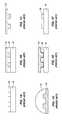
- a stamp substrate 10 having a resist 12 thereoncreates a pattern on a surface of the stamp substrate 10 .
- An elastomer casing 14conventionally formed from polydimethylsiloxane, is deposited over the stamp substrate 10 and resist 12 and cured.
- the stamp substrate 10 and resist 12are separated from the cured elastomer casing 14 to form a soft stamp 14 ′ with topographical features.
- the soft stamp 14 ′includes a pattern that corresponds to the pattern in the resist 12 , which pattern is to be formed on the semiconductor device.
- the soft stamp 14 ′is then wetted with an ink 16 and brought into contact with a receptor substrate 18 .
- the inkis physisorbed on the soft stamp 14 ′ and is transferred to the receptor substrate 18 to form SAMs 20 .
- FIG. 1FTheoretically, the SAMs 20 are formed only in regions where the ink 16 contacts the receptor substrate 18 .
- the physisorbed nature of the ink 16leads to poor resolution of the stamped features on the receptor substrate 18 as ink 16 not in contact with the receptor substrate 18 wicks down the soft stamp 14 ′ due to capillary action.
- Another disadvantageis that the stamped features are no smaller than the lithographically defined features of the soft stamp 14 ′.
- FIGS. 1A-1Care cross-sectional views of a soft stamp during various stages of fabrication according to conventional process techniques
- FIGS. 1D-1Fare cross-sectional views of a soft stamp during microcontact printing according to conventional process techniques
- FIG. 2is a flow chart of an embodiment of fabricating and using a stamp of the present invention
- FIG. 3is a cross-sectional view of an embodiment of a stamp of the present invention with an ink material chemisorbed to the stamp;
- FIG. 4is a cross-sectional view of a stamp-ink material-receptor substrate complex according to an embodiment of the present invention
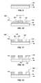
- FIGS. 5-18are cross-sectional views of embodiments of stamp structures or intermediate stamp structures of the present invention during various stages of fabrication
- FIG. 19is a cross-sectional view of an embodiment of a stamp of the present invention including self-assembled block copolymer domains.
- FIGS. 20A , 20 B and 20 Care cross-sectional views of an embodiment of a receptor substrate including self-assembled monolayers thereon.
- a stampmay be prepared or selected such that at least one region of a stamping surface of the stamp has chemical affinity for an ink material, as indicated at 1000 in FIG. 2 .
- chemical affinitymeans and includes the tendency of a molecule to associate with another molecule based on chemical forces between the molecules.
- the region of chemical affinity on the stamping surfaceforms a pattern that mirrors a desired pattern to be formed on a receptor substrate.
- the term “receptor substrate”means and includes semiconductor substrates, silicon wafers, silicon on insulator (“SOI”) substrates, silicon on sapphire (“SOS”) substrates, epitaxial layers of silicon on a base semiconductor foundation and other semiconductor materials such as silicon-germanium, germanium, gallium arsenide and indium phosphide.
- the receptor substrateincludes silicon dioxide.
- any electrically conductive, electrically nonconductive, or electrically semiconductive material forming a solid phase at room temperatureas long as the receptor substrate and the ink material are capable of chemically bonding.
- the stamping surfaceincludes at least a first region having chemical affinity for the ink material. Other regions of the stamping surface may lack chemical affinity for the ink material or may have a different chemical affinity for the ink material, such as substantially less chemical affinity.
- the region of chemical affinityprovides the stamping surface with at least one region of chemical differentiation, which has different chemical properties than the other regions of the stamping surface.
- the region of chemical differentiationenables the stamping surface to chemically react with at least a portion of the ink material.
- the region of chemical differentiationmay be formed by depositing a material having chemical affinity for the ink material on the stamp, or by modifying the deposited material or the stamping surface to include moieties or functional groups having chemical affinity for the ink material.
- the region of chemical differentiation on the stamping surfacemay include, for example, gold, thiol functional groups or amine functional groups.
- an embodiment of stamp 300may include the regions of chemical differentiation 52 and the stamp substrate 50 .
- the stamping surface of the stamp 300may be substantially planar with at least one region of chemical differentiation 52 thereon, with the remainder of the stamping surface lacking chemical affinity for the ink material.
- the stamping surfacemay include topographical features wherein peak tips of the topographical features have chemical affinity for the ink material. As such, the peak tips correspond to the regions of chemical differentiation 52 .
- the peak tipsmay be formed from a different material than the other portions of the stamp 300 .
- the regions of chemical differentiation 52include a region of gold.
- the regions of chemical differentiation 52include a region formed from another inorganic material, such as silicon dioxide, modified with thiol or amine functional groups.
- the regions of chemical differentiation 52include domains of a self-assembled block copolymer.
- the block copolymer surfacemay be modified to include, for example, gold, thiol or amine functional groups.
- the ink material (I-X-Y)is also shown in FIG. 3 , attached to the stamp 300 through the regions of chemical differentiation 52 . Additional details of the ink material and of fabricating the stamp 300 are described herein.
- the ink materialis selected such that the chemical affinity between the stamping surface and the ink material is less than the chemical affinity between the ink material and the receptor substrate.
- the ink materialmay be any material to be deposited on the receptor substrate and capable of forming a pattern, such as a SAM, on the receptor substrate.
- the ink materialmay be a small molecule with the ability to function as a SAM.
- the ink materialmay include at least one functional group that chemically reacts with the region of chemical differentiation 52 on the stamping surface.
- the ink materialmay also include at least one functional group that chemically reacts with the receptor substrate.
- the ink materialmay be mono-functional, bi-functional or more.
- the ink materialhas two or more functional groups on opposite ends of the ink material, providing orthogonal reactivity.
- orthogonal reactivitymeans and includes at least one functional group on the ink material that reacts in a first manner and at least one functional group on the ink material that is inert or reacts in a second, different manner under the same conditions.
- the ink materialmay have a composition of I-X-Y, where “I” includes a first functional group capable of binding to the region of chemical differentiation 52 , “X” is a spacer or linker molecule and “Y” includes a second functional group capable of binding to the receptor substrate. Any portion of I and Y may include the functional group capable of bonding to the stamping surface or the receptor substrate. For instance, a terminal portion of I or a terminal portion of Y may include the desired functional group, or an interior portion of I or an interior portion of Y may include the desired functional group. Additional ink materials other than those described herein may be used as long as portions “I” and “Y” are present in such a manner that they do not interfere with each other's respective binding or with the creation of the pattern on the receptor substrate.
- the spacer (X) of the ink materialmay be selected to provide a particular thickness of the resultant pattern on the receptor substrate. Any spacer that does not disrupt binding of the ink material to the region of chemical differentiation 52 and receptor substrate is suitable.
- the spacermay be a polar, nonpolar, positively charged, negatively charged, or uncharged molecule.
- a saturated or unsaturated, linear or branched alkyl, aryl, or other hydrocarbon spacermay be used, as well as corresponding halogenated hydrocarbons, especially fluorinated hydrocarbons.
- the ink materialmay be 2-aminoethanethiol, aminothiophenol, cysteine, homocysteine, leucinethiol, 2-butylaminoethanethiol, 2-cyclohexylaminoethanethiol, a mercapto alcohol, e.g., 2-mercaptoethanol (HS—CH 2 CH 2 OH) or 4-mercapto-1-butanol, acetylenic thiol, an aliphatic or aromatic thiol, lactic acid, hydroxybutyric acid, hydroxyisocaproic acid, hydroxyisophthallic acid, 8-hydroxy-7-iodo-5-quinolinesulfonic acid, hydroxymandelic acid, hydroxymethanesulfinic acid, a hydroxybenzoic acid, hydroxynapthalenesulfonic acid, hydroxypentadecanoic acid, hydroxyundecanoic acid, an acetylenic carboxy
- 2-mercaptoethanol
- the stamping surfaceis wetted with the ink material.
- Physisorbed ink materialis removed from the stamping surface while chemisorbed ink material remains on the regions of chemical differentiation 52 .
- the tam “physisorbed” and grammatical equivalents thereofmeans and includes the physical adsorption of a molecule, such as the ink material, to a surface, such as the stamping surface.
- the physisorbed ink materialmay be adhered to the stamping surface through weak intermolecular interactions, such as Van der Waals forces.
- the term “chemisorbed” and grammatical equivalents thereofmeans and includes the chemical adsorption of a molecule, such as the ink material, to a surface, such as the stamping surface.
- the chemisorbed ink materialmay be chemically bonded to the stamping surface, such as through hydrogen bonds, ionic bonds, dithiol linkages, electrostatic bonds or any other so-called “weak” chemical bond.
- the stampmay be washed under conditions that remove the physisorbed ink material, but do not remove the chemisorbed ink material due to the chemical affinity of the ink material for the regions of chemical differentiation 52 .
- the washis preferably a non-polar organic solvent that has at least some ability to solvate the ink material. Polar solvents tend to disrupt the chemisorbed ink.
- a washmay be performed for approximately 0.1 to 1 minute at a temperature up to the boiling point of the solvent or ink material.
- the ink materialmay be removed by heating the ink material-stamp complex so as to boil off the physisorbed ink.
- the ink material-stamp complexmay be exposed to a high vacuum so as to pull off physisorbed ink without removing the chemisorbed ink material.
- FIG. 3depicts an embodiment of a stamp 300 having chemisorbed ink material (I-X-Y) on the regions of chemical differentiation 52 . Thus, the ink material is only in contact with the regions of chemical differentiation 52 .
- the stamping surfacemay be wetted with the ink material under conditions, which enable the ink material to react chemically with the regions of chemical differentiation 52 .
- the ink materialmay be coated onto the stamping surface by any convenient method.
- the ink materialmay be directly contacted with the stamping surface or the ink material may be absorbed onto a piece of paper and the stamping surface may be pressed against the piece of paper.
- a cotton swab or the likemay be used to transfer ink material to the stamping surface. Ink material may be rapidly transferred to the stamping surface.
- the stamping surfaceFor example, contacting the stamping surface with ink material for a period of time of approximately 6 to 600 seconds is sufficient to enable the ink material to chemisorb to the region of chemical differentiation 52 . However, contact may be maintained for substantially longer periods of time to ensure that the ink material reacts with the region of chemical differentiation 52 .
- the “I” portion of the ink materialmay react with the stamping surface, forming hydrogen bonds, ionic bonds, dithiol linkages, electrostatic bonds, or any other so-called “weak” chemical bond.
- the stampincludes gold regions of chemical differentiation 52 thereon and reacts with the ink material having at least one sulfur-containing functional group, such as a thiol functional group.
- the ink materialmay be applied to the stamping surface using a non-aqueous medium.
- a non-aqueous mediumFor example, if the ink material and stamping surface interact via acid/base interaction, exposure to a polar solvent may interfere with the ink material binding to the stamping surface.
- the ink materialmay be dissolved in a solvent for transfer to the stamping surface.
- the ink materialmay be transferred to the stamping surface in a solvent at a concentration of less than 0.001 mM, preferably from about 1 to about 10 k mM. Any solvent within which the ink material is substantially soluble, and which allows the ink material to chemically bind to the stamping surface, may be used.
- the stamping surfacemay, optionally, be exposed to more than one ink material where the second ink material may be chemically distinct from the first ink material.
- the exposure to the second ink materialmay be substantially simultaneous with the introduction of the first ink material or may be separate.
- the second ink materialmay chemically react with second regions of chemical differentiation that are distinct from the regions of chemical differentiation 52 that bind to the first ink material.
- the stamp 300 having the ink material chemisorbed to the region of chemical differentiation 52is brought into contact with a receptor substrate 200 , forming a stamping surface-ink material-receptor substrate complex 400 .
- the receptor substrate 200may, optionally, include an additional material layer thereon to improve wettability of the receptor substrate 200 .
- the Y portion of the ink materialmay form a chemical bond with the receptor substrate 200 .
- the bonds between the ink material and the receptor substrate 200may be covalent, ionic or polar bonds.
- the chemical bonds between the stamping surface and the ink materialmay have a weaker bond strength than those between the ink material and the receptor substrate 200 .
- the stamp 300may be contacted with the receptor substrate 200 under appropriate conditions to transfer the ink material from the stamping surface to desired regions on the receptor substrate 200 .
- the temperature during ink material transfer to the receptor substratemay be selected to maximize the rate of binding without cleaving the ink material-receptor substrate or ink material-stamping surface bonds.
- the ink material-receptor substrate bondsmay form prior to cleaving the ink material-stamping surface bonds.
- Selection of the appropriate range of temperaturesis within the skill of one in the art and depends upon the particular ink material and receptor substrate. Generally, suitable temperatures will range from room temperature to near boiling point of the ink material.
- the stamping surface and the receptor surface 200may be contacted under conditions that enable chemical bonds to form between the receptor substrate 200 and the ink material.
- the stamping surface-ink material-receptor substrate complexremains intact for approximately 1 minute to 240 minutes. For example, 15 minutes may be adequate for microcontact printing using Huisgens-1,3-dipolar cycloaddition reaction.
- the stamping surface-ink material-receptor substrate complex 400may be exposed to conditions which eliminate or disrupt the chemical affinity between the regions of chemical differentiation 52 on the stamping surface and the ink material, while the chemical affinity between the ink material and the receptor substrate 200 may be substantially unaffected by the conditions.
- the bonds between the stamp 300 and the ink materialmay be cleaved thermally, oxidatively, electrochemically, or by exposure to a polar, protic solvent.
- the regions of chemical differentiation 52include gold or thiol groups
- the bonds between the stamp 300 and the ink materialmay be cleaved thermally, oxidatively, or electrochemically.
- the regions of chemical differentiation 52include acid/base groups
- the bonds between the stamp 300 and the ink materialmay be cleaved by exposure to a polar, protic solvent.
- an aqueous solutionis introduced into channels between the topographical features to cleave the bonds between the stamp 300 and the ink material.
- the aqueous solutionmay be introduced into voids 130 ′ to break the bonds between the ink material and the stamp 300 .
- the bonds between the ink material and the regions of chemical differentiation 52are cleaved by applying heat to the stamping surface-ink material-receptor substrate complex 400 .
- the bonds between the ink material and the regions of chemical differentiation 52are cleaved by contacting the stamping surface-ink material-receptor substrate complex 400 with a solution having a high ionic strength. In another embodiment, the bonds between the ink material and the regions of chemical differentiation 52 are cleaved by contacting the stamping surface-ink material-receptor substrate complex 400 with a solution having a high ionic strength and applying heat. The bonds between the ink material and the regions of chemical differentiation 52 may be cleaved without cleaving most of the bonds between the ink material and the receptor substrate 200 .
- the stamp 300may be removed from the receptor substrate 200 , leaving ink material (which may form, for example, SAMs) on portions of the receptor substrate 200 in contact with the regions of chemical differentiation 52 of the stamping surface.
- the stamp 300may then be prepared and re-inked for further receptor substrate stamping.
- the stamp 300may be exposed to hydrogen peroxide or bleach to oxidize the thiol functional groups to sulfonic acid, cleaving the ink material from the gold regions of chemical differentiation 52 .
- the gold-thiol bondsare relatively weak (20 Kcal/mol-35 Kcal/mol) as compared to potential C—N, C—O, Si—O or Si—N bonds between the ink material and the receptor substrate 200 , the gold-thiol bonds may be cleaved without disrupting the ink material/receptor substrate bonds.
- Other methods of cleaving the gold-thiol bondinclude thermal cleavage and electrochemical cleavage.
- the disulfide bonds between the stamp 300 and the ink materialmay be cleaved by reductive conditions including (1) exposure to metallic zinc; (2) electrochemical reduction or (3) exposure to other thiols (e.g., thiol-disulfide rearrangement discussed herein).
- Dithiothreitolis a particularly useful reagent for reducing disulfides to thiols in this manner.
- the stamp 300includes amine regions of chemical differentiation 52 (e.g., aminoalkyl(trialkoxy)silanes) and the ink contains carboxyl or other acid group
- the acid-base interactionmay be broken by exposure to a polar, protic solvent (e.g., water, methanol, ethanol, formic acid, hydrogen fluoride, ammonia or combinations thereof).
- a polar, protic solvente.g., water, methanol, ethanol, formic acid, hydrogen fluoride, ammonia or combinations thereof.
- applying the ink material to the stamp 300 and contacting the stamp 300 and the receptor substrate 200may occur in the absence of a polar, protic solvent.
- a polar aprotic solvente.g., dimethyl sulfoxide, dimethylformamide, or hexamethylphosphorotriamide
- a polar aprotic solventmay be present during the stamping, if miscible with polar, protic solvents that disrupt the stamp-ink material bond, which is dried after the stamping.
- Table 1is a non-limiting, exemplary list of materials that may be used in combination as the regions of chemical differentiation 52 , the receptor substrate 200 and the ink material.
- the ink materialmay react with the regions of chemical differentiation 52 and the receptor substrate 200 to form the stamping surface-ink material-receptor substrate complex 400 .
- the ink material/stamping surface and ink material/receptor substrate combinationmay be selected based on conventional understanding of chemical interactions and bond strengths.
- the stamp 300may be formed by any conventional method that produces the desired pattern on the stamping surface, which pattern mirrors the pattern to be formed on the receptor substrate 200 .
- the pattern on the stamping surfaceis defined by the regions of chemical differentiation 52 , which have chemical affinity for the ink material.
- the pattern on the stamp 300may be formed by conventional techniques, such as by using a mold or by photolithography or e-beam lithography.
- the pattern on the stamp 300may also be formed using block copolymers.
- the stamp 300is created lithographically, such as by using, for example, photoresist materials or e-beam resist materials.
- a film 70may be deposited on the stamp substrate 50 .
- the film 70may provide the regions of chemical differentiation 52 by using a material for film 70 that has chemical affinity for the ink material.
- the material used to form the film 70may be chemically modified to include functional groups having chemical affinity for the ink material.
- the film 70may be formed from gold, an inorganic material, such as silicon dioxide, or a block copolymer.
- a resist layer 180may be deposited over the film 70 and patterned by conventional photolithographic or e-beam lithographic techniques, forming openings 72 .
- Photoresist materials, e-beam resist materials and lithographic techniquesare well known in the art and, therefore, forming the pattern in the resist layer 180 is not discussed in detail herein.
- the resist materialmay be a positive or negative resist and may be an organic or an inorganic material including, but not limited to, polystyrene based resists, poly(meth)acrylate based resists, silsesquioxane materials (“SSQ”) and combinations thereof.
- the resist layer 180may be formed over the film 70 by a conventional coating technique including, but not limited to, dip coating, bar coating, spin coating, roll coating, spray coating, and flow coating depending on the material used in the resist layer 180 .
- the pattern in the resist layer 180may be transferred to the film 70 using resist layer 180 as a mask, as known in the art.
- the film 70may be etched to produce the stamping surface 70 ′ on the stamp substrate 50 . While the stamp 300 is illustrated in FIG. 6 as including topographical features, the stamp 300 may be substantially planar. If the material used as film 70 has affinity for the ink material, such as gold, the stamping surface 70 ′ may correspond to regions of chemical differentiation 52 .
- the stamping surface 70 ′may be modified to include a layer of gold or to include functional groups, such as thiol or amine groups, that have affinity for the ink material.
- the modified stamping surface 70 ′may correspond to the regions of chemical differentiation 52 .
- silicon dioxide or block copolymersare used as the material of film 70
- the film 70may be modified with a layer of gold or with thiol or amine groups to provide the regions of chemical differentiation 52 .
- the regions of chemical differentiation 52are formed from gold.
- goldmay be used as the material of film 70 or gold is used to coat another material used as film 70 .
- E-beam lithographymay be used to create the stamp 300 by depositing a resist layer 180 over the stamp substrate 50 . The pattern produced in the resist layer 180 may be transferred to the stamp substrate 50 as known in the art.
- a film 70 ′′′ including a chromium layer (75 nm) followed by a layer of gold (5 nm)is deposited over the resist layer 180 . Any metals deposited under the gold layer, such as the chromium layer, may have little or no affinity for thiol groups.
- the chromium layermay be used as an adhesive layer for the gold.
- the resist layer 180 and overlying metalmay then be removed, such as by ultrasonication for 20 minutes in toluene.
- the resulting stamp 300 ′′′′′′′ having gold regions of chemical differentiation 52 thereon(corresponding to the stamping surface 70 ′) may be dried, for example, in a nitrogen stream. Since gold has affinity for thiol groups, the stamp 300 may be used with an ink material having thiol functional groups to pattern the receptor substrate 200 .
- SAMs of ink material or gold regions of chemical differentiation 52may enable complete or substantially complete patterns of ink material to be formed on the receptor substrate 200 , such that a better transfer of the ink material to the receptor substrate 200 may occur relative to the stamps that do not form complete SAMs.
- the film 70is formed from an inorganic material including, or modified to include, exposed thiol or amine functional groups thereon.
- the film 70may be formed from silicon dioxide and coated with a mercaptopropyl(trialkoxy)silane compound (e.g., CAS Nos. 14814-09-6, 4420-74-0, available from Gelest Inc., Morrisville, Pa.).
- the coating of the mercaptopropyl(trialkoxy)silane compoundmay provide exposed thiol groups on the stamp 300 , which correspond to the regions of chemical differentiation 52 .
- a silicon dioxide filmmay be deposited on the stamp substrate 50 and patterned by conventional techniques to form topographic features.
- silicon dioxidemay be the material used for film 70 .
- the silicon oxide filmmay be patterned by (1) conventional photolithography (i.e., down to 60 nm) of photoresist followed by dry etch; (2) e-beam lithography (down to ⁇ 30 nm) of e-beam resist followed by dry etch; (3) graphoepitaxial self-assembly of a block copolymer and removal of one domain to form an etch mask followed by dry etch as further described herein; or (4) pitch multiplication.
- the silicon oxide filmmay be a thin coating on the stamp substrate 50 .
- the silicon oxide filmmay be between about 1-10 nm thick.
- the majority of the etchoccurs into a separate material that does not react with mercaptopropyl(trialkoxy)silane, such as silicon.
- This materialforms the non-reactive areas around the regions of chemical differentiation 52 .
- the patterned silicon oxide filmmay then be exposed to the mercaptopropyl(trialkoxy)silane compound so as to form a thiol-containing layer on the surface of the silicon dioxide.
- a thiolsilane monolayermay be deposited on the silicon oxide film prior to patterning such that the thiolsilane monolayer survives the etching process (e.g., the thiolsilane monolayer is covered by the resist during patterning) and such that the thiol groups are exclusively on the stamp tips and not on the sides of the topographical features.
- the thiolsilane monolayeris deposited over a patterned substrate, the thiolsilane monolayer will likely be deposited on the sidewalls of any topographical features of the stamp and the ink material may be deposited on the sidewalls of the topographical features.
- the thiolsilane monolayeris deposited prior to patterning, the thiolsilane monolayer, and thus the thiol groups, will be exclusively on the stamp tips.
- the film 70may be formed from silicon oxide and coated with an aminoalkyl(trialkoxy)silane compound (available from Gelest, Inc., Morrisville, Pa.).
- the coating of the aminoalkyl(trialkoxy)silane compoundmay provide exposed amine groups on the stamp 300 , which correspond to the regions of chemical differentiation 52 .
- the method of creating the stamp 300 coated with the aminoalkyl(trialkoxy)silane compoundmay follow the general method described above with respect to the stamp 300 coated with the mercaptopropyl(trialkoxy)silane compound.
- the patterned silicon oxide filmmay be exposed to the aminoalkyl(trialkoxy)silane compound to form an amine layer of the silicon oxide film surface.
- an aminosilane monolayeris formed on the silicon oxide film prior to patterning such that the aminosilane monolayer survives the etching process to create regions of chemical affinity including amine groups exclusively on the stamp tips and not on the sides of the topographical features.
- the film 70is formed from a block copolymer.
- the film 70 formed from the block copolymermay be modified with gold or at least one of thiol and amine functional groups to provide the stamping surface 70 ′, which corresponds to the regions of chemical differentiation 52 .
- one of the blocksinherently contains a thiol or amine functional group, for example, polyvinylpyridine.
- a first block of the block copolymermay be selected, or modified to include, at least one functional group that reacts with a first ink material, while the second block may be inert or, optionally, may include at least one functional group that reacts with a second functional group of a second ink material. Alternatively, or in addition to, the second block may be removed prior to contacting the stamping surface with the ink material.
- block copolymersare used for film 70 , one domain of the block domain may be selectively removed to form openings 72 as discussed herein. Alternatively, a planar device may be formed wherein one domain lacks affinity for the ink material.
- Films 70 formed from the block copolymermay self-assemble into periodic structures by microphase separation of the constituent blocks after annealing. Following self-assembly, one block of the block copolymer may be selectively removed, producing a patterned film formed from the remaining block. The patterned film may be used as an etch mask for patterning features onto the underlying substrate. Alternatively, one block of the block copolymer may have chemical affinity for the first ink material while the other block(s) may have chemical affinity for the second ink material.
- the stampis made from a PS-PMMA block copolymer
- the ink materialis alkynethiol-gold nanoparticles
- the receptor substrateis 11-azidoundecyl(trialkokysilane) on SiO 2 .
- the alkynethiol gold nanoparticleswill selectively absorb to the PS domains of the PS-PMMA block copolymer film by selective wetting of the PS over PMMA by the alkyne tails on the nanoparticles.
- Block copolymersare polymers that include at least one long sequence (i.e., “block”) of the same monmeric unit(s) covalently bound to at least one long sequence (i.e., “block”) of unlike type e.g., including differing monomeric unit(s).
- Block copolymersare conventionally named using the word “-block-” or “-b-” to separate each monomeric unit, while random copolymers are conventionally named using the term “-random-” or an “-r-” to separate each monomeric unit.
- block copolymersare contemplated herein including diblock copolymers (copolymers having two blocks), triblock copolymers (copolymers having three blocks), multiblock copolymers (copolymers having more than three blocks), and combinations thereof.
- each block of the block copolymermay differ from other blocks not only in terms of the structure of the monomeric units that form that block, but also in other properties including, for example, physical properties (e.g., mechanical strength, surface tension, wettability, and/or solubility) and chemical properties (e.g., solubility, chemical reactivity, susceptibility to removal techniques and/or susceptibility to cross-linking reactions).
- Film morphology, including the size and shape of the microphase-separated domainsmay be controlled by the molecular weight and volume fraction of the blocks in the diblock copolymer.
- the ratio of each block of a diblock copolymeris between about 40:60 and about 60:40 to create lamellar domains or alternating stripes of the blocks. Domain sizes of the blocks may be between about 5 nm and about 50 nm.
- the block copolymer used in creating the stamp 300 ′may be selected based on their chemical affinity toward the ink material.
- the blocks of the block copolymermay be polybutadiene-polybutylmethcrylate, polybutadiene-polydimethylsiloxane, poly(styrene-b-methyl methacrylate) (PS-b-PMMA), polybutadiene-polymethylmethacrylate, polybutadiene-polyvinylpyridine, polybutylmethacrylate-polybutylacrylate, polybutylmethacrylate-polyvinylpyridine, polybutadienepolyvinylpyridine, polyethyleneoxide-polyisoprene, polyethyleneoxide-polybutadiene, polyethyleneoxide-polystyrene, polyethylene-polyvinylpyridine, polyisoprene-polymethylmethacrylate, polyisoprene-polyvinylpyridine, polybutylacrylate-polymethylmethacrylate, polybutylacrylate-poly
- the block copolymermay be a diblock copolymer.
- block copolymers having three (a triblock copolymer) or more (a multiblock copolymer) blocksmay also be used.
- triblock copolymersinclude, but are not limited to, poly(styrene-block methyl methacrylate-block-ethylene oxide) and block copolymers having three or more blocks selected from the following: polystyrene, polymethylmethacrylate, polyethyleneoxide, polyisoprene, polybutadiene, poly lactic acid, polyvinylpyridine, and combinations thereof.
- the block copolymeris a diblock copolymer.
- Diblock copolymersmay be symmetric (i.e., the volume fraction of the first block is substantially the same as the volume fraction of the second block) or asymmetric (i.e., the volume fraction of the first block is substantially different than the volume fraction of the second block).
- each block of a symmetric diblock copolymerhas a volume fraction of from about 0.4 to about 0.6.
- each block of an asymmetric diblock copolymerhas a volume fraction less than about 0.4 or greater than about 0.6.
- the diblock copolymeris a symmetric diblock copolymer and is used for embodiments in which the diblock copolymer self-assembles to form lamellae (i.e., sheets of material interleaved with another material).
- Asymmetric diblock copolymersmay be used for embodiments in which the diblock copolymer self-assembles to form other morphologies including, for example, spheres, cylinders, gyroids, or combinations thereof.
- both the first and the second block copolymersmay be symmetric block copolymers.
- the stamp 300may be created using diblock copolymers, which are applied to the surface of the stamp substrate 50 by any suitable means. Any material, which may permit the diblock copolymer to orient in a substantially perpendicular manner, may be used for the stamp substrate 50 .
- substantially perpendicular lamellaerefers to a set of lamellae that are, on average, perpendicular to the surface.
- other materialsmay be used for the stamp substrate 50 if the surface of the stamp substrate 50 is treated with a material that may permit the diblock copolymer to orient substantially perpendicularly thereto.
- the stamp substrate 50is not limited to any particular material.
- the diblock copolymermay be applied to the stamp substrate 50 by conventional techniques including, for example, deposition methods, coating methods, transfer methods, and/or other available application methods.
- the diblock copolymermay be applied by spin coating, dip coating, spray coating, and combinations thereof In such methods, the diblock copolymer may be dissolved, dispersed, or suspended in a medium (e.g., a solvent).
- the solution, dispersion, or suspensionmay be deposited on the stamp substrate 50 , and the medium may be optionally removed (e.g., through evaporation at ambient or elevated temperature, and at ambient or reduced pressure) during or subsequent to deposition.
- the blocks of the diblock copolymermay microphase separate on a nanometer-scale length scale, forming a hexagonal array of pores in a thin polymer film.
- Other phase morphologies of the diblock copolymerinclude, but are not limited to, a spherical phase, a lamellar phase, etc.
- At least one region of chemical differentiationis formed on a stamp substrate, the at least one region of chemical differentiation exhibiting chemical affinity for at least one ink material.
- the at least one region of chemical differentiationmay include gold, a compound containing at least one thiol functional group or a compound containing at least one amine functional group.
- the at least one region of chemical differentiation on the stamp substratemay be formed by depositing a block copolymer on the stamp substrate and self-assembling the block copolymer into at least two domains having a perpendicular orientation to the stamp substrate. At least one of the domains of the self-assembled block copolymer may be optionally removed. At least one of the domains may be coated with gold, a compound containing thiol functional groups, a compound containing amine functional groups, or combinations thereof.
- the at least one region of chemical differentiationmay include topographical features.
- the stamp substrate 50is provided having a neutral wetting surface with respect to each block of the diblock copolymer. As such, no block of the block copolymer preferentially wets the surface of the stamp substrate 50 .
- the stamp substrate 50may be formed from one of the materials previously described. While the stamp substrate 50 is depicted as being substantially planar, the stamp substrate 50 may be patterned prior to deposition of the diblock copolymer. For example, the stamp substrate 50 may include trenches that serve as guides for the formation of self-assembled block copolymers therein. The trenches may be formed using conventional lithographic techniques or using block copolymers, as described in detail herein.
- the stamp substrate 50is chemically patterned to include a series of chemical regions of about the same size of each block in the block copolymer, which serve as guides for the formation of the self-assembled block copolymers therein.
- a symmetric diblock copolymermay be deposited on the stamp substrate 50 , forming film 70 ′′. If the stamp substrate 50 does not have a neutral wetting surface, a material layer 60 may be formed between the stamp substrate 50 and the film 70 ′′, providing the neutral wetting surface. While material layer 60 is shown in FIG. 9 , this layer is optional.
- the material layer 60is hydrogen-terminated silicon, which provides the neutral wetting surface for the diblock copolymer polystyrene-b-polymethylmethacrylate.
- the material layer 60includes a random copolymer and may be cross-linked using the same or different methods than used to cross-linking at least one block of the block copolymer. The cross-linked material layer 60 may be used, for example, to render the stamp substrate 50 neutral wetting with respect to each block of the block copolymer, enabling the block copolymer to self-assemble on the stamp substrate 50 .
- the diblock copolymeris a polystyrene-b-polymethylmethacrylate diblock copolymer
- a cross-linkable polystyrene-r-polymethylmethacrylate random copolymermay be used as the material layer 60 .
- the cross-linked material layer 60is preferably resistant to further processing encountered during the block copolymer self-assembly process.
- the diblock copolymermay be annealed to break up existing domains and allow the diblock copolymer to self-assemble.
- the diblock polymermay be annealed by thermal annealing, solvent annealing, or combinations thereof. During the annealing, the diblock polymer may form ordered domains having nanometer-scale dimensions.
- Thermal annealingmay include exposing the diblock copolymer to an elevated temperature (e.g., at or above the glass transition temperature of the diblock copolymer), and lowering the temperature to allow the self-assembled block copolymer to harden.
- the diblock polymermay be thermally annealed by heating the diblock copolymer to a temperature of from about 0° C. to about 250° C. for up to about 24 hours or longer, preferably under a vacuum or inert atmosphere.
- Solvent annealingmay include exposing the diblock copolymer to a solvent until the diblock copolymer swells. At least a portion of the solvent may then be removed, such as through evaporation.
- each block of the diblock copolymer in the film 70 ′′may self-assemble into a domain during the anneal.
- Symmetric diblock copolymersself-assemble into lamellar structures in which alternating lamellae each represent a domain including one block of the diblock copolymer.
- a distance between the middle of a first lamella and the middle of the next lamella of the same typeis the inherent periodicity (L o ) of the diblock copolymer, which is dependent on the length and/or molecular weight of the polymer chain for each block.
- the inherent periodicity of the diblock copolymermay be increased by increasing the length and/or molecular weight of the polymer chain for one or both diblocks of the diblock copolymer.
- the L omay be decreased by decreasing the length and/or molecular weight of the polymer chain for one or both block of the diblock copolymer.
- Diblock copolymers contemplated hereinmay have an L o from about 10 nm to about 100 nm.
- the L o of the first block copolymermay be the same as or different from the L o of the second block copolymer.
- the diblock copolymer in the film 70 ′′self-assembles during the anneal to form a set of alternating lamellae 110 and 120 that are substantially perpendicular to the stamp substrate 50 .
- the lamellae 110 , 120may have differentiated chemical affinities in that lamellae 110 may have affinity for a first ink material while lamellae 120 may be substantially inert or may have affinity for a second ink material.
- Each block of the diblock copolymermay be selected to provide the desired chemical affinity for the ink material(s), or one or more of the blocks may be modified with a functional group to provide the desired chemical affinity.
- the upper surface of the lamellae 110 , 120as shown in the stamp 300 ′ of FIG.
- the lamellae 110 , 120may correspond to the regions of chemical differentiation 52 .
- the upper surface of one of lamellae 110 or 120may be modified to include gold, thiol groups or amine groups to provide the regions of chemical differentiation 52 .
- lamellae 120maybe removed to create a pattern on the stamp 300 ′′, as shown in FIG. 11 .
- lamellae 110may be cross-linked, for example, by exposure to radiation, e.g., ultraviolet (UV) radiation.
- Cross-linked lamellaemay have, for example, improved mechanical properties and lower susceptibility to removal during further processing.
- the block of the block copolymer that forms lamellae 110may be susceptible to cross-linking without the addition of a cross-linking agent.
- the block copolymeris a polystyrene-b-polymethylmethacrylate diblock copolymer
- the polystyrene blockmay be cross-linked by exposure to UV radiation.
- the block of the block copolymer that forms lamellae 110may be made cross-linkable by including a small amount (e.g., 1 to 5 mole %) of a thermally cross-linkable monomer (e.g., a benzocyclobutane-containing monomer) or a photochemically cross-linkable monomer (e.g., divinyl benzene or azido-methylstyrene).
- a thermally cross-linkable monomere.g., a benzocyclobutane-containing monomer
- a photochemically cross-linkable monomere.g., divinyl benzene or azido-methylstyrene
- the cross-linking agentmay be added to the block of the block copolymer that forms lamellae 110 .
- cross-linking agentsinclude, for example, the combination of a cross-linker (e.g., 1,3,5-trimethyl-2,4,6-(triacetoxymethyl)benzene) and a thermal acid generator (e.g., cyclohexylmethyl(2-oxocycicohexyl)sulfonium trifluoromethanesulfonate).
- the lamellae 120which are not cross-linked, may be selectively removed, leaving the cross-linked lamellae 110 and voids 130 on the surface of the stamp 300 ′′.
- the voids 130are defined by sidewalls 150 of the cross-linked lamellae 110 .
- methods for removing uncross-linked lamellaeare known in the art including, for example, irradiation (e.g., UV or electron beam), ozone treatment, wet chemical processing methods, such as immersion in a solvent, and/or etching methods such as reactive ion etching and ion beam etching.
- the lamellae including the polystyrene blocksmay be selectively removed, for example, by acetic acid development after a blanket exposure to ultraviolet (UV) radiation.
- UV radiationultraviolet
- the resulting stamp 300 ′′may be used for printing or may be subjected to further processing, for example, wherein the stamp 300 ′′ functions as a mask.
- material 170may be selectively deposited over the cross-linked lamellae 110 .
- the material 170may have a different etch selectivity than lamellae 110 .
- the material 170may be gold that is deposited using a grazing angle deposition. Gold may be sputtered onto the surface at an angle of a few degrees above parallel to the stamping substrate 50 . The gold will be deposited above lamellae 110 and to a small extent within voids 130 at the top of the sidewalls.
- the bottom surface 135 of voids 130will be largely protected from gold deposition by the adjacent lamellae 110 and a stamp 300 ′′′ including gold regions of chemical differentiation 52 on the cross-linked lamellae 110 may be formed. ( FIG. 13 ).
- the cross-linked lamellae 110 of the stamp 300 ′′may also be used as a mask for further processing.
- the voids 130may be filled with a material prior to stamping the receptor substrate 200 .
- material 170may be deposited within the voids 130 and over the cross-linked lamellae 110 .
- the material 170may have a different etch selectivity than lamellae 110 .
- the material 170may be an inorganic material, such as silicon dioxide or gold.
- the material 170may be planarized, exposing the top surface of lamellae 110 .
- the lamellae 110may be selectively removed, leaving a pattern of the material 170 on the stamp substrate 50 and voids 130 , as shown in FIG.
- an inorganic materialsuch as gold may be deposited on the top surfaces of the material 170 or the top surfaces of the material 170 may be modified prior to selective etching of lamellae 110 to include thiol or amine functional groups, forming regions of chemical differentiation 52 on the material 170 .
- the voids 130 of FIG. 11may form trenches that serve as guides for self-assembly of the block copolymers.
- trenchesmay be formed by conventional lithography and used as guides for the self-assembly of the block copolymers.
- a second block copolymer 170 ′which may be the same as or different than the block copolymer used in film 70 ′′, may be deposited in the voids 130 .
- the voids 130have a bottom surface (an exposed surface of the stamp substrate 50 ) that is neutral wetting with respect to each block of the second block copolymer 170 ′.
- the material layer 60may, optionally, be deposited therein to render the stamp substrate 50 surface neutral wetting, as previously described.
- the sidewalls 150may be wetted by at least one block of the second block copolymer 170 ′ (e.g., one block of the second block copolymer 170 ′ is similar to, or the same as, the cross-linked block of the lamellae 110 ).
- the second block copolymer 170 ′may be annealed, by methods such as those previously described, to allow self-assembly within each void 130 to form a second set of alternating lamellae 142 and 144 , as shown in FIG. 16 .
- the lamellae 142 , 144may be oriented substantially perpendicular to the stamp substrate 50 and substantially in register with each sidewall 150 , forming stamp 300 ′′′′.
- lamellae 142may be cross-linked by methods such as those previously described.
- uncross-linked lamellae 144may be removed by methods such as those previously described, forming a pattern of lamellae 142 .
- the resulting patternmay be used, for example, as an etch mask to form sub-lithographic openings in the stamp substrate 50 .
- the term “sub-lithographic”means and includes having one or more sizes or dimensions that are less than the minimum sizes or dimensions obtainable using conventional lithography.
- the patternmay form stamp 300 ′′′′′. The stamps 300 ′′′′′, 300 ′′′′′ shown in FIGS.
- 16 and 17may be used for patterning the receptor substrate 200 , provided that two of lamellae 110 , 142 and 144 , as shown in FIG. 16 , have chemical affinity for the desired ink material.
- the ink materialmay bind to all three regions and no pattern would be transferred to the receptor substrate 200 .
- the ink materialmay bind to these two regions, forming a pattern, which may be transferred to the receptor substrate 200 .
- the lamellae 110 , 142 shown in FIG. 17may have chemical affinity for the same ink material or the lamellae 110 , 142 may have chemical affinity for different ink materials.
- the diblock copolymeris used with the stamp of FIG. 6 by depositing the diblock copolymer within openings 72 formed by film 70 .
- the diblock copolymeris annealed, forming alternating lamellae 210 , 220 that are substantially perpendicular to the stamp substrate 50 of the stamp 300 ′′′′′′. ( FIG. 18 ).
- the lamellae 210 , 220may provide regions of chemical differentiation in addition to those that are provided by film 70 ′.
- the upper surface thereofmay be modified to include gold, thiol groups or amine groups to provide the additional regions of chemical differentiation.
- one of the sets of lamellae in the openings 72may be cross-linked and removed, by methods such as those previously described, forming a desired pattern in the openings 72 .
- film 70is a silicon-containing layer such that film 70 has silicon-containing sidewalls 150 .
- the film 70may be formed from silicon dioxide (SiO 2 ), silicon nitride (Si 3 N 4 ), SSQ, Si, SiOC, SiON or combinations thereof.
- a homopolymer of one block of the diblock copolymermay be grafted to the silicon-containing sidewalls 150 so that openings 72 may be preferentially wetted by the same block of the diblock copolymer.
- the diblock copolymer to be self-assembled in the openings 72is a polystyrene-b-polymethylmethacrylate diblock copolymer
- a polystyrene homopolymermay be grafted to the silicon-containing sidewalls 150 so that the openings 72 may be wetted by the polystyrene block of the diblock copolymer.
- a polymethylmethacrylate homopolymermay be grafted to the silicon-containing sidewalls 150 so that openings 72 may be preferentially wetted by the polymethylmethacrylate block of the diblock copolymer.
- the homopolymersmay be grafted by a wide variety of methods known in the art including, for example, preparing homopolymers with end groups (e.g., hydroxyl groups) that may interact (e.g., by forming hydrogen and/or covalent bonds) with the silicon-containing sidewalls.
- end groupse.g., hydroxyl groups
- the first and second blocks of the diblock copolymer in these stampsprovide regions of chemical differentiation that react with the first and second ink materials, respectively.
- the first and second blocks of the diblock copolymer in these stampsform separate domains having sizes and morphologies that correspond to the stamp pattern.
- the first block of the diblock copolymeris selected, or modified to include, a functional group that reacts with the first ink material and the second block is selected, or modified to include, a functional group that reacts with the second ink material.
- the stamp substrate 50includes thereon a first domain 110 ′ selective to “I” (the first ink material) and a second domain 120 ′ selective to “I*” (the second ink material).
- the stamps 300 ′, 300 ′′′′, 300 ′′′′′, 300 ′′′′′′may be used to pattern the receptor substrate 200 with the first and second ink materials. While use of two ink materials is shown with respect to stamps 300 ′, 300 ′′′′, 300 ′′′′′, 300 ′′′′′′, the use of more than two ink materials may be contemplated if the stamp includes more than two distinct regions of chemical differentiation.
- the first and second ink materialmay be applied to the stamps during the same printing process or during a separate printing process.
- the stamp, ink material or receptor substratemay be formed from other materials and may include other combinations of materials, as previously described.
- the stampmay include gold regions of chemical differentiation and interact with the ink material via a gold-thiol bond.
- the stampmay interact with the stamping surface via disulfide bonds.
- a disulfide bondis relatively weak (between about 50 Kcal/mol and about 60 Kcal/mol).
- the ink materialmay include a free thiol (R—SH) functional group, in which case an oxidant, such as bromine, may be used to form the disulfide linkage to the regions of chemical differentiation on the stamp.
- an oxidantsuch as bromine
- the ink materialmay be present in excess in an oxidized dithiol form R—S—S—R, and a thiol-disulfide rearrangement reaction may be used to transfer the ink material to the stamp, according to the following reaction:
- Stamp-SiO 2propyl—SH+R—S—S—R ⁇ Stamp-SiO 2 —propyl—S—S—R+HS—R
- aminesmay be present in the ink material and may be employed to bond the receptor substrate and the ink material.
- the receptor substratemay be a SiO 2 receptor substrate grafted with a glycidoxypropyl(trialkoxy)silane compound, (e.g. CAS Nos.
- the ink materialmay include 2-aminoethanethiol, aminothiophenol, cysteine, homocysteine, leucinethiol, 2-butylaminoethanethiol, or 2-cyclohexylaminoethanethiol (all available from Sigma-Aldrich, Inc., St. Louis, Mo.).
- the receptor substratemay be SiO 2 grafted with a isocyanatopropyl(trialkoxy)silane compound (available from Gelest, Inc., Morrisville, Pa.) and the ink material may be 2-aminoethanethiol, aminothiophenol, cysteine, homocysteine, leucinethiol, 2-butylaminoethanethiol, or 2-cyclohexylaminoethanethiol (all available from Sigma-Aldrich, Inc., St. Louis, Mo.).
- the receptor substrate and the ink materialmay react to form urea linkers.
- any mercapto alcohole.g., 2-mercaptoethanol (HS—CH 2 CH 2 OH) or 4-mercapto-1-butanol, may be used to form urethane linkers.
- Huisgens-1,3-dipolar cycloadditionmay be employed using a SiO 2 receptor substrate grafted with 6-azidosulfonylhexyl (triethoxy)silane or 11-azidoundecyl group monolayers formed by grafting 11-bromoundecyl(triethoxy)silane (available from Gelest) to SiO2, then derivatizing with sodium azide (available from Gelest, Inc., Morrisville, Pa.).
- the ink materialmay be an acetylenic thiol and may be prepared, for example, by reaction of 1,4-butanedithiol or 1,2-ethanethiol with 0.5 eq.
- Nucleophilic attack on a Si—Cl surfaceis another chemistry that may be used to bond the receptor substrate and the ink material.
- the receptor substratemay be Si—Cl, which is formed from H-terminated silicon via C1 2 gas exposure at 80° C. or Cl 2 gas exposure with illumination with a tungsten lamp.
- the ink materialmay include 2-aminoethanethiol, aminothiophenol, cysteine, homocysteine, leucinethiol, 2-butylaminoethanethiol, or 2-cyclohexylaminoethanethiol (all available from Sigma-Aldrich, Inc., St. Louis, Mo.) or any mercapto alcohol, e.g., 2-mercaptoethanol (HS—CH 2 CH 2 OH) or 4-mercapto-1-butanol.
- the receptor substratemay be SiO 2 grafted with 6-azidosulfonylhexyl (triethoxy)silane available from Gelest, Inc., Morrisville, Pa. or SiO2 grafted with an azidoalkly as described herein.
- the ink materialmay be an aliphatic or aromatic thiol.
- the azido group on the surface of the receptor substratemay decompose to a nitrene above 110° C. and the nitrene may react with proximate functional groups of the ink material.
- the stampmay utilize an acid-base interaction with the ink material and the stamp may be formed of SiO 2 topographic features coated with material to create exposed amine groups, such as an aminoalkyl(trialkoxy)silane compound.
- the receptor substratemay be SiO 2 grafted with an isocyanatopropyl(trialkoxy)silane available from Gelest, Inc., Morrisville, Pa.
- the ink materialmay be, for example, lactic acid, hydroxybutyric acid, hydroxyisocaproic acid, hydroxyisophthallic acid, 8-hydroxy-7-iodo-5-quinolinesulfonic acid, hydroxymandelic acid, hydroxymethanesulfinic acid, hydroxybenzoic acids, hydroxynapthalenesulfonic acid, hydroxypentadecanoic acid, or hydroxyundecanoic acid.
- Huisgens-1,3-dipolar cycloadditionmay also be utilized with the stamp having aminoalkyl(trialkoxy)silane regions of chemical differentiation thereon.
- the receptor substratemay be SiO 2 grafted with 6-azidosulfonylhexyl (triethoxy)silane available from Gelest, Inc or derivatized with an azidoalkyl as known in the art.
- the ink materialmay be any acetylenic carboxylate or sulfonate, e.g. propiolic acid, 4-butynoic acid, 5-pentynoic acid, etc.
- the receptor substratemay be Si—Cl, which is formed as previously described.
- the ink materialmay be, by way of non-limiting example, lactic acid, hydroxybutyric acid, hydroxyisocaproic acid, hydroxyisophthallic acid, 8-hydroxy-7-iodo-5-quinolinesulfonic acid, hydroxymandelic acid, hydroxymethanesulfinic acid, hydroxybenzoic acids, hydroxynapthalenesulfonic acid, hydroxypentadecanoic acid, or hydroxyundecanoic acid.
- Nitrene insertionmay also be utilized with a stamp having aminoalkyl(trialkoxy)silane regions of chemical differentiation thereon.
- the receptor substratemay be SiO 2 grafted with 6-azidosulfonylhexyl (triethoxy)silane available from Gelest, Inc., Morrisville, Pa. or with an azidoalkyl, and the ink material may be any aliphatic or aromatic thiol moiety.
- the stamp ( 300 - 300 ′′′′′′′) produced by any of the above-mentioned embodimentsmay be used to pattern the receptor substrate 200 , such as by nanocontact chemical printing.
- the stampmay be used to print SAMs on a surface of the receptor substrate 200 .
- the pattern on the receptor substrate 200may have identical, or substantially identical, resolution to the pattern on the stamp.
- the pattern on the stampmay be used to produce features on the receptor substrate 200 that are sub-lithographic.
- the pattern on the stampmay have a pitch of between about 10 nm and about 100 nm, producing features between about 5 nm and about 50 nm on the receptor substrate 200.
- the pattern on the stampis about 14 nm or less, producing features on the receptor substrate 200 having a size of about 14 nm or less.
- the pattern formed on the receptor substrate 200may be a first SAM 210 .
- the ink material deposited on the receptor substrate 200 by the stampmay form the first SAM 210 that corresponds to the pattern on the stamping surface, thus providing a differentiated pattern on the receptor substrate 200 .
- the first SAM 210may have a thickness of less than about 20 ⁇ (2 nm), which is affected by the selection of the ink material and, in particular, the spacer thereof.
- the first SAM 210has a lateral width less than about 60 nm. In one embodiment, the first SAM 210 has a lateral width of about 14 nm.
- the lateral width of the SAMscorresponds to the feature size of the stamping surface.
- further processingmay proceed as desired.
- Conventional techniqueswhich are not described in detail herein, may be used to produce a semiconductor structure that includes the receptor substrate 200 and the first SAM 210 .
- portions of the receptor substrate 200 adjacent the first SAM 210may remain free of the ink material that produces the first SAM 210 .
- These exposed portions of the receptor substrate 200may be subjected to further etching or plating.
- the first SAM 210may be used as an etch mask on the receptor substrate 200 or may be used to guide selective deposition on the receptor substrate 200 .
- the first SAM 210may also be used to direct vapor deposition.
- oxidefor example, may be selectively deposited on portions of the receptor substrate 200 lacking the first SAM 210 .
- materialmay be deposited exclusively on the first SAM 210 or exclusively on portions of the receptor substrate 200 lacking the first SAM 210 .
- the receptor substrate 200may also be treated with a second ink material that is chemically distinct from the first ink material used to form the first SAM 210 , creating a second SAM 220 thereon, as shown in FIG. 20B .
- the second ink materialmay be one of the ink materials described herein.
- a block copolymer with domains selective to the first SAM 210 and second SAM 220 , respectively, and with domain sizes and morphologies that match stamp patternmay be deposited over the first SAM 210 and the second SAM 220 .
- Deposition and self-assembly of this diblock copolymermay proceed as previously discussed to form a second set of alternating lamellae 310 and 320 that are substantially perpendicular to the surface of the receptor substrate, as shown in FIG. 20C . Further processing may proceed as described herein. For example, one of the lamellae 310 , 320 may be removed and used as either an etch mask or a mask to guide deposition of further materials.
- the SAMs 210 , 220 patterned on the receptor substrate 200may be used for guiding selective deposition of materials and for chemical patterning of block copolymers cast onto it, which may in turn serve as etch masks. While the latter application may seem redundant given that the stamp may have been prepared using block copolymers, the advantage is that lithographic definition of features will be required for the stamp, whereas multiple patterned receptor substrates may be prepared from a single stamp without further lithography. For example, patterning a substrate using conventional lithographically and/or sub-lithographic techniques has been hampered by difficulties including, for example, high costs and/or incompatibility with high throughput production methods.
- a stampmay be prepared using conventional lithography, because the stamp may be used to pattern multiple substrates, the production cost per substrate is reduced and the rate of formation of block copolymers on the receptor substrate is greatly reduced.
Landscapes
- Engineering & Computer Science (AREA)
- Nanotechnology (AREA)
- Chemical & Material Sciences (AREA)
- Physics & Mathematics (AREA)
- General Physics & Mathematics (AREA)
- Crystallography & Structural Chemistry (AREA)
- Condensed Matter Physics & Semiconductors (AREA)
- Theoretical Computer Science (AREA)
- Mathematical Physics (AREA)
- Manufacturing & Machinery (AREA)
- Mechanical Engineering (AREA)
- Exposure Of Semiconductors, Excluding Electron Or Ion Beam Exposure (AREA)
- Manufacture Or Reproduction Of Printing Formes (AREA)
- Printing Plates And Materials Therefor (AREA)
- Laminated Bodies (AREA)
- Shaping Of Tube Ends By Bending Or Straightening (AREA)
Abstract
Description
- This application is a divisional of U.S. patent application Ser. No. 11/787,928, filed Apr. 18, 2007, pending, the disclosure of which is hereby incorporated herein by this reference in its entirety. This application is also related to U.S. patent application Ser. No. 11/766,663, filed Jun. 21, 2007, for DIBLOCK COPOLYMER FILMS FOR USE AS ANTIREFLECTION COATING, FOR POLYMER MIRRORS, AND FOR POLYMER BAND PASS FILTERS and U.S. patent application Ser. No. 12/259,921, filed Oct. 28, 2008, for METHODS FOR THE DOMAIN SPECIFIC STAINING OF SELF-ASSEMBLED BLOCK COPOLYMER FILMS WITH METAL OXIDES.
- Embodiments of the invention relate to semiconductor fabrication and, more specifically, to methods, a stamp and a system for patterning a substrate.
- As the development of nanoscale semiconductor devices and systems increase, new processes and materials are needed to fabricate such semiconductor devices and components. While feature sizes on the semiconductor devices are decreasing, the cost of lithographic tools is increasing exponentially. Further reductions in feature size are often restricted by the lower limit of dimensions that can be achieved using lithographic methods. Semiconductor devices having features of about 60 nanometers (nm) or less, which are referred to herein as “sub-lithographic” features, are difficult to produce using conventional lithography.
- Microcontact printing is one method for creating sub-lithographic features on semiconductor devices. The technique creates self-assembled monolayers (SAMs) on specific sites on a surface of a substrate of the semiconductor device. In a conventional process, a master mold with topographical features is prepared by photolithography or electron (e-beam) lithography. Referring to
FIG. 1A , astamp substrate 10 having aresist 12 thereon creates a pattern on a surface of thestamp substrate 10. Anelastomer casing 14, conventionally formed from polydimethylsiloxane, is deposited over thestamp substrate 10 and resist12 and cured. Thestamp substrate 10 andresist 12 are separated from the curedelastomer casing 14 to form asoft stamp 14′ with topographical features. (FIGS. 1B and 1C ) Thesoft stamp 14′ includes a pattern that corresponds to the pattern in theresist 12, which pattern is to be formed on the semiconductor device. Thesoft stamp 14′ is then wetted with anink 16 and brought into contact with areceptor substrate 18. (FIG. 1D ) The ink is physisorbed on thesoft stamp 14′ and is transferred to thereceptor substrate 18 to formSAMs 20. (FIG. 1F ) Theoretically, theSAMs 20 are formed only in regions where theink 16 contacts thereceptor substrate 18. However, the physisorbed nature of theink 16 leads to poor resolution of the stamped features on thereceptor substrate 18 asink 16 not in contact with thereceptor substrate 18 wicks down thesoft stamp 14′ due to capillary action. Another disadvantage is that the stamped features are no smaller than the lithographically defined features of thesoft stamp 14′. - Attempts have been made to prepare sub-lithographic features on semiconductor devices by other methods known in the art. For example, e-beam lithography and extreme ultraviolet (EUV) lithography have been used in attempts to prepare such sub-lithographic features. However, widespread use of such methods has been hampered by difficulties including, for example, high costs and/or incompatibility with high throughput production methods. Accordingly, improved methods and systems for preparing sub-lithographic features on semiconductor devices are desired, as are stamps for achieving same.
FIGS. 1A-1C are cross-sectional views of a soft stamp during various stages of fabrication according to conventional process techniques;FIGS. 1D-1F are cross-sectional views of a soft stamp during microcontact printing according to conventional process techniques;FIG. 2 is a flow chart of an embodiment of fabricating and using a stamp of the present invention;FIG. 3 is a cross-sectional view of an embodiment of a stamp of the present invention with an ink material chemisorbed to the stamp;FIG. 4 is a cross-sectional view of a stamp-ink material-receptor substrate complex according to an embodiment of the present invention;FIGS. 5-18 are cross-sectional views of embodiments of stamp structures or intermediate stamp structures of the present invention during various stages of fabrication;FIG. 19 is a cross-sectional view of an embodiment of a stamp of the present invention including self-assembled block copolymer domains; andFIGS. 20A ,20B and20C are cross-sectional views of an embodiment of a receptor substrate including self-assembled monolayers thereon.- The following description with reference to the drawings describes embodiments of devices and methods according to the invention. Such description is for illustrative purposes only and not for purposes of limiting the same. Other embodiments of the present invention are contemplated and encompassed thereby.
- An embodiment of a method of the present invention for patterning a substrate is disclosed, as are embodiments of a stamp and a patterning system of the present invention. According to one embodiment, a stamp may be prepared or selected such that at least one region of a stamping surface of the stamp has chemical affinity for an ink material, as indicated at1000 in
FIG. 2 . As used herein, the term “chemical affinity” means and includes the tendency of a molecule to associate with another molecule based on chemical forces between the molecules. The region of chemical affinity on the stamping surface forms a pattern that mirrors a desired pattern to be formed on a receptor substrate. As used herein, the term “receptor substrate” means and includes semiconductor substrates, silicon wafers, silicon on insulator (“SOI”) substrates, silicon on sapphire (“SOS”) substrates, epitaxial layers of silicon on a base semiconductor foundation and other semiconductor materials such as silicon-germanium, germanium, gallium arsenide and indium phosphide. In one embodiment, the receptor substrate includes silicon dioxide. However, a wide variety of materials may be used as the receptor substrate, such as any electrically conductive, electrically nonconductive, or electrically semiconductive material forming a solid phase at room temperature, as long as the receptor substrate and the ink material are capable of chemically bonding. - The stamping surface includes at least a first region having chemical affinity for the ink material. Other regions of the stamping surface may lack chemical affinity for the ink material or may have a different chemical affinity for the ink material, such as substantially less chemical affinity. The region of chemical affinity provides the stamping surface with at least one region of chemical differentiation, which has different chemical properties than the other regions of the stamping surface. The region of chemical differentiation enables the stamping surface to chemically react with at least a portion of the ink material. The region of chemical differentiation may be formed by depositing a material having chemical affinity for the ink material on the stamp, or by modifying the deposited material or the stamping surface to include moieties or functional groups having chemical affinity for the ink material. The region of chemical differentiation on the stamping surface may include, for example, gold, thiol functional groups or amine functional groups.
- As illustrated in
FIG. 3 , an embodiment ofstamp 300 may include the regions ofchemical differentiation 52 and thestamp substrate 50. The stamping surface of thestamp 300 may be substantially planar with at least one region ofchemical differentiation 52 thereon, with the remainder of the stamping surface lacking chemical affinity for the ink material. Alternatively, the stamping surface may include topographical features wherein peak tips of the topographical features have chemical affinity for the ink material. As such, the peak tips correspond to the regions ofchemical differentiation 52. The peak tips may be formed from a different material than the other portions of thestamp 300. Regardless of whether the stamping surface is substantially planar or includes topographical features, in one embodiment, the regions ofchemical differentiation 52 include a region of gold. In another embodiment, the regions ofchemical differentiation 52 include a region formed from another inorganic material, such as silicon dioxide, modified with thiol or amine functional groups. In another embodiment, the regions ofchemical differentiation 52 include domains of a self-assembled block copolymer. The block copolymer surface may be modified to include, for example, gold, thiol or amine functional groups. The ink material (I-X-Y) is also shown inFIG. 3 , attached to thestamp 300 through the regions ofchemical differentiation 52. Additional details of the ink material and of fabricating thestamp 300 are described herein. - As indicated at1020 of
FIG. 2 , the ink material is selected such that the chemical affinity between the stamping surface and the ink material is less than the chemical affinity between the ink material and the receptor substrate. The ink material may be any material to be deposited on the receptor substrate and capable of forming a pattern, such as a SAM, on the receptor substrate. By way of non-limiting example, the ink material may be a small molecule with the ability to function as a SAM. The ink material may include at least one functional group that chemically reacts with the region ofchemical differentiation 52 on the stamping surface. The ink material may also include at least one functional group that chemically reacts with the receptor substrate. The ink material may be mono-functional, bi-functional or more. In one embodiment, the ink material has two or more functional groups on opposite ends of the ink material, providing orthogonal reactivity. As used herein, the term “orthogonal reactivity” means and includes at least one functional group on the ink material that reacts in a first manner and at least one functional group on the ink material that is inert or reacts in a second, different manner under the same conditions. - The ink material may have a composition of I-X-Y, where “I” includes a first functional group capable of binding to the region of
chemical differentiation 52, “X” is a spacer or linker molecule and “Y” includes a second functional group capable of binding to the receptor substrate. Any portion of I and Y may include the functional group capable of bonding to the stamping surface or the receptor substrate. For instance, a terminal portion of I or a terminal portion of Y may include the desired functional group, or an interior portion of I or an interior portion of Y may include the desired functional group. Additional ink materials other than those described herein may be used as long as portions “I” and “Y” are present in such a manner that they do not interfere with each other's respective binding or with the creation of the pattern on the receptor substrate. - The spacer (X) of the ink material may be selected to provide a particular thickness of the resultant pattern on the receptor substrate. Any spacer that does not disrupt binding of the ink material to the region of
chemical differentiation 52 and receptor substrate is suitable. The spacer may be a polar, nonpolar, positively charged, negatively charged, or uncharged molecule. By way of non-limiting example, a saturated or unsaturated, linear or branched alkyl, aryl, or other hydrocarbon spacer may be used, as well as corresponding halogenated hydrocarbons, especially fluorinated hydrocarbons. By way of non-limiting example, the ink material may be 2-aminoethanethiol, aminothiophenol, cysteine, homocysteine, leucinethiol, 2-butylaminoethanethiol, 2-cyclohexylaminoethanethiol, a mercapto alcohol, e.g., 2-mercaptoethanol (HS—CH2CH2OH) or 4-mercapto-1-butanol, acetylenic thiol, an aliphatic or aromatic thiol, lactic acid, hydroxybutyric acid, hydroxyisocaproic acid, hydroxyisophthallic acid, 8-hydroxy-7-iodo-5-quinolinesulfonic acid, hydroxymandelic acid, hydroxymethanesulfinic acid, a hydroxybenzoic acid, hydroxynapthalenesulfonic acid, hydroxypentadecanoic acid, hydroxyundecanoic acid, an acetylenic carboxylate or sulfonate, e.g., propiolic acid, 4-butynoic acid, or 5-pentynoic acid, or combinations thereof. - As indicated at1030 and1040 of
FIG. 2 , the stamping surface is wetted with the ink material. Physisorbed ink material is removed from the stamping surface while chemisorbed ink material remains on the regions ofchemical differentiation 52. As used herein, the tam “physisorbed” and grammatical equivalents thereof means and includes the physical adsorption of a molecule, such as the ink material, to a surface, such as the stamping surface. The physisorbed ink material may be adhered to the stamping surface through weak intermolecular interactions, such as Van der Waals forces. As used herein, the term “chemisorbed” and grammatical equivalents thereof means and includes the chemical adsorption of a molecule, such as the ink material, to a surface, such as the stamping surface. The chemisorbed ink material may be chemically bonded to the stamping surface, such as through hydrogen bonds, ionic bonds, dithiol linkages, electrostatic bonds or any other so-called “weak” chemical bond. For example, the stamp may be washed under conditions that remove the physisorbed ink material, but do not remove the chemisorbed ink material due to the chemical affinity of the ink material for the regions ofchemical differentiation 52. - For hydrogen bonds, electrostatic or acid/base interaction, the wash is preferably a non-polar organic solvent that has at least some ability to solvate the ink material. Polar solvents tend to disrupt the chemisorbed ink. A wash may be performed for approximately 0.1 to 1 minute at a temperature up to the boiling point of the solvent or ink material. In some embodiments, the ink material may be removed by heating the ink material-stamp complex so as to boil off the physisorbed ink. Alternatively, the ink material-stamp complex may be exposed to a high vacuum so as to pull off physisorbed ink without removing the chemisorbed ink material.
FIG. 3 depicts an embodiment of astamp 300 having chemisorbed ink material (I-X-Y) on the regions ofchemical differentiation 52. Thus, the ink material is only in contact with the regions ofchemical differentiation 52. - The stamping surface may be wetted with the ink material under conditions, which enable the ink material to react chemically with the regions of
chemical differentiation 52. The ink material may be coated onto the stamping surface by any convenient method. By way of non-limiting example, the ink material may be directly contacted with the stamping surface or the ink material may be absorbed onto a piece of paper and the stamping surface may be pressed against the piece of paper. Alternately, a cotton swab or the like may be used to transfer ink material to the stamping surface. Ink material may be rapidly transferred to the stamping surface. For example, contacting the stamping surface with ink material for a period of time of approximately 6 to 600 seconds is sufficient to enable the ink material to chemisorb to the region ofchemical differentiation 52. However, contact may be maintained for substantially longer periods of time to ensure that the ink material reacts with the region ofchemical differentiation 52. The “I” portion of the ink material may react with the stamping surface, forming hydrogen bonds, ionic bonds, dithiol linkages, electrostatic bonds, or any other so-called “weak” chemical bond. In one embodiment, the stamp includes gold regions ofchemical differentiation 52 thereon and reacts with the ink material having at least one sulfur-containing functional group, such as a thiol functional group. - Depending on the nature of the bonds that form between the stamping surface and ink material, the ink material may be applied to the stamping surface using a non-aqueous medium. For example, if the ink material and stamping surface interact via acid/base interaction, exposure to a polar solvent may interfere with the ink material binding to the stamping surface. In other embodiments, the ink material may be dissolved in a solvent for transfer to the stamping surface. The ink material may be transferred to the stamping surface in a solvent at a concentration of less than 0.001 mM, preferably from about 1 to about 10 k mM. Any solvent within which the ink material is substantially soluble, and which allows the ink material to chemically bind to the stamping surface, may be used.
- The stamping surface may, optionally, be exposed to more than one ink material where the second ink material may be chemically distinct from the first ink material. The exposure to the second ink material may be substantially simultaneous with the introduction of the first ink material or may be separate. As described in more detail herein, the second ink material may chemically react with second regions of chemical differentiation that are distinct from the regions of
chemical differentiation 52 that bind to the first ink material. - As indicated at1050 of
FIG. 2 and illustrated inFIG. 4 , thestamp 300 having the ink material chemisorbed to the region ofchemical differentiation 52 is brought into contact with areceptor substrate 200, forming a stamping surface-ink material-receptor substrate complex 400. As described in detail below, thereceptor substrate 200 may, optionally, include an additional material layer thereon to improve wettability of thereceptor substrate 200. Upon contact, the Y portion of the ink material may form a chemical bond with thereceptor substrate 200. The bonds between the ink material and thereceptor substrate 200 may be covalent, ionic or polar bonds. The chemical bonds between the stamping surface and the ink material may have a weaker bond strength than those between the ink material and thereceptor substrate 200. Thestamp 300 may be contacted with thereceptor substrate 200 under appropriate conditions to transfer the ink material from the stamping surface to desired regions on thereceptor substrate 200. The temperature during ink material transfer to the receptor substrate may be selected to maximize the rate of binding without cleaving the ink material-receptor substrate or ink material-stamping surface bonds. Thus, the ink material-receptor substrate bonds may form prior to cleaving the ink material-stamping surface bonds. Selection of the appropriate range of temperatures is within the skill of one in the art and depends upon the particular ink material and receptor substrate. Generally, suitable temperatures will range from room temperature to near boiling point of the ink material. The stamping surface and thereceptor surface 200 may be contacted under conditions that enable chemical bonds to form between thereceptor substrate 200 and the ink material. In one embodiment, the stamping surface-ink material-receptor substrate complex remains intact for approximately 1 minute to 240 minutes. For example, 15 minutes may be adequate for microcontact printing using Huisgens-1,3-dipolar cycloaddition reaction. - As indicated at1060 of
FIG. 2 , the stamping surface-ink material-receptor substrate complex 400 may be exposed to conditions which eliminate or disrupt the chemical affinity between the regions ofchemical differentiation 52 on the stamping surface and the ink material, while the chemical affinity between the ink material and thereceptor substrate 200 may be substantially unaffected by the conditions. The bonds between thestamp 300 and the ink material may be cleaved thermally, oxidatively, electrochemically, or by exposure to a polar, protic solvent. By way of non-limiting example, if the regions ofchemical differentiation 52 include gold or thiol groups, the bonds between thestamp 300 and the ink material may be cleaved thermally, oxidatively, or electrochemically. If, however, the regions ofchemical differentiation 52 include acid/base groups, the bonds between thestamp 300 and the ink material may be cleaved by exposure to a polar, protic solvent. - In one embodiment, if the stamping surface includes topographical features, which correspond to the regions of
chemical differentiation 52, an aqueous solution is introduced into channels between the topographical features to cleave the bonds between thestamp 300 and the ink material. By way of non-limiting example, referring toFIG. 4 , the aqueous solution may be introduced intovoids 130′ to break the bonds between the ink material and thestamp 300. In another embodiment, the bonds between the ink material and the regions ofchemical differentiation 52 are cleaved by applying heat to the stamping surface-ink material-receptor substrate complex 400. In one embodiment, the bonds between the ink material and the regions ofchemical differentiation 52 are cleaved by contacting the stamping surface-ink material-receptor substrate complex 400 with a solution having a high ionic strength. In another embodiment, the bonds between the ink material and the regions ofchemical differentiation 52 are cleaved by contacting the stamping surface-ink material-receptor substrate complex 400 with a solution having a high ionic strength and applying heat. The bonds between the ink material and the regions ofchemical differentiation 52 may be cleaved without cleaving most of the bonds between the ink material and thereceptor substrate 200. Thestamp 300 may be removed from thereceptor substrate 200, leaving ink material (which may form, for example, SAMs) on portions of thereceptor substrate 200 in contact with the regions ofchemical differentiation 52 of the stamping surface. Thestamp 300 may then be prepared and re-inked for further receptor substrate stamping. - By way of non-limiting example, if the
stamp 300 has gold regions ofchemical differentiation 52 and the ink material includes thiol functional groups, thestamp 300 may be exposed to hydrogen peroxide or bleach to oxidize the thiol functional groups to sulfonic acid, cleaving the ink material from the gold regions ofchemical differentiation 52. Since the gold-thiol bonds are relatively weak (20 Kcal/mol-35 Kcal/mol) as compared to potential C—N, C—O, Si—O or Si—N bonds between the ink material and thereceptor substrate 200, the gold-thiol bonds may be cleaved without disrupting the ink material/receptor substrate bonds. Other methods of cleaving the gold-thiol bond include thermal cleavage and electrochemical cleavage. - By way of non-limiting example, if the
stamp 300 has regions ofchemical differentiation 52 that include thiol functional groups (e.g., mercaptopropyl(trialkoxy)silanes), the disulfide bonds between thestamp 300 and the ink material may be cleaved by reductive conditions including (1) exposure to metallic zinc; (2) electrochemical reduction or (3) exposure to other thiols (e.g., thiol-disulfide rearrangement discussed herein). Dithiothreitol is a particularly useful reagent for reducing disulfides to thiols in this manner. - By way of non-limiting example, if the
stamp 300 includes amine regions of chemical differentiation52 (e.g., aminoalkyl(trialkoxy)silanes) and the ink contains carboxyl or other acid group, the acid-base interaction may be broken by exposure to a polar, protic solvent (e.g., water, methanol, ethanol, formic acid, hydrogen fluoride, ammonia or combinations thereof). In this situation, applying the ink material to thestamp 300 and contacting thestamp 300 and thereceptor substrate 200 may occur in the absence of a polar, protic solvent. A polar aprotic solvent (e.g., dimethyl sulfoxide, dimethylformamide, or hexamethylphosphorotriamide) may be present during the stamping, if miscible with polar, protic solvents that disrupt the stamp-ink material bond, which is dried after the stamping. - Table 1 is a non-limiting, exemplary list of materials that may be used in combination as the regions of
chemical differentiation 52, thereceptor substrate 200 and the ink material. The ink material may react with the regions ofchemical differentiation 52 and thereceptor substrate 200 to form the stamping surface-ink material-receptor substrate complex 400. TABLE 1 Materials for the Regions of Chemical Differentiation, Inks, and Receptor Substrates Regions of Chemical Differentiation Ink Material Receptor Substrate Gold 2-aminoethanethiol, aminothiophenol, SiO2grafted with a cysteine, homocysteine, leucinethiol, glycidoxypropyl(trialkoxy)silane 2-butylaminoethanethiol, or 2-cyclohexylaminoethanethiol Gold To form urea linkers: SiO2grafted with an 2-aminoethanethiol, aminothiophenol, isocyanatopropyl(trialkoxy)silane cysteine, homocysteine, leucinethiol, 2-butylaminoethanethiol, or 2-cyclohexylaminoethanethiol to form urethane linkers: any mercapto alcohol, e.g., 2- mercaptoethanol (HS—CH2CH2OH) or 4-mercapto-1-butanol Gold Any acetylenic thiol SiO2grafted with 6-azidosulfonyl-hexyl(triethoxy) silane or SiO2 grafted with 11-bromoundecyl (triethoxy) silane and further reacted with sodium azide Gold 2-aminoethanethiol, aminothiophenol, Si—Cl from H-terminated silicon cysteine, homocysteine, leucinethiol, 2-butylaminoethanethiol, 2-cyclohexylaminoethanethiol, any mercapto alcohol, e.g., 2-mercaptoethanol (HS—CH2CH2OH) or 4-mercapto-1-butanol Gold Any aliphatic or aromatic thiol SiO2grafted with 6-azidosulfonyl-hexyl(triethoxy) silane or SiO2 grafted with 11-bromoundecyl (triethoxy) silane and further reacted with sodium azide Thiol Group 2-aminoethanethiol, aminothiophenol, SiO2grafted with a cysteine, homocysteine, leucinethiol, glycidoxy-propyl(trialkoxy) silane 2-butylaminoethanethiol, or 2-cyclohexylaminoethanethiol Thiol Group To form urea linkers: SiO2grafted with an 2-aminoethanethiol, aminothiophenol, isocyanatopropyl(trialkoxy) silane cysteine, homocysteine, leucinethiol, 2-butylaminoethanethiol, or 2-cyclohexylaminoethanethiol To form urethane linkers: any mercapto alcohol, e.g., 2-mercaptoethanol (HS—CH2CH2OH) or 4-mercapto-1-butanol Thiol Group Any acetylenic thiol e.g., N SiO2grafted with (2-mercaptoethyl) propiolamide 6-azidosulfonyl-hexyl(triethoxy) silane silane or SiO2 grafted with 11-bromoundecyl (triethoxy) silane and further reacted with sodium azide Thiol Group 2-aminoethanethiol, aminothiophenol, Si—Cl from H-terminated silicon cysteine, homocysteine, leucinethiol, 2-butylaminoethanethiol, 2-cyclohexylaminoethanethiol or any mercapto alcohol, e.g., 2-mercaptoethanol (HS—CH2CH2OH) or 4-mercapto-1-butanol Thiol Group Any aliphatic or aromatic thiol SiO2grafted with 6-azidosulfonyl-hexyl(triethoxy) silane or SiO2 grafted with 11-bromoundecyl (triethoxy) silane and further reacted with sodium azide Amine Group lactic acid, hydroxybutyric acid, SiO2grafted with an hydroxyisocaproic acid, isocyanatopropyl(trialkoxy) silane hydroxyisophthallic acid, 8-hydroxy-7-iodo-5-quinolinesulfonic acid, hydroxymandelic acid, hydroxymethanesulfinic acid, hydroxybenzoic acids, hydroxynapthalenesulfonic acid, hydroxypentadecanoic acid, or hydroxyundecanoic acid Amine Group any acetylenic carboxylate or sulfonate, SiO2grafted with e.g., propiolic acid, 4-butynoic acid, 6-azidosulfonyl-hexyl(triethoxy) 5-pentynoic acid, etc. silane silane or SiO2 grafted with 11-bromoundecyl (triethoxy) silane and further reacted with sodium azide Amine Group lactic acid, hydroxybutyric acid, Si—Cl from H-terminated silicon hydroxyisocaproic acid, hydroxyisophthallic acid, 8-hydroxy-7-iodo-5-quinolinesulfonic acid, hydroxymandelic acid, hydroxymethanesulfinic acid, hydroxybenzoic acids, hydroxynapthalenesulfonic acid, hydroxypentadecanoic acid, or hydroxyundecanoic acid Amine Group Any aliphatic or aromatic thiol SiO2grafted with 6-azidosulfonyl-hexyl(triethoxy) silane or SiO2 grafted with 11-bromoundecyl (triethoxy) silane and further reacted with sodium azide - Although Table 1 identifies certain ink materials having orthogonal reactivity, many functional groups in the ink materials are suitable for use with materials with which they are not categorized in Table 1. Any and all such combinations are within the scope of the present invention. The ink material/stamping surface and ink material/receptor substrate combination may be selected based on conventional understanding of chemical interactions and bond strengths. The
stamp 300 may be formed by any conventional method that produces the desired pattern on the stamping surface, which pattern mirrors the pattern to be formed on thereceptor substrate 200. The pattern on the stamping surface is defined by the regions ofchemical differentiation 52, which have chemical affinity for the ink material. By way of non-limiting example, the pattern on thestamp 300 may be formed by conventional techniques, such as by using a mold or by photolithography or e-beam lithography. The pattern on thestamp 300 may also be formed using block copolymers. In one embodiment, thestamp 300 is created lithographically, such as by using, for example, photoresist materials or e-beam resist materials. Referring toFIG. 5 , afilm 70 may be deposited on thestamp substrate 50. Thefilm 70 may provide the regions ofchemical differentiation 52 by using a material forfilm 70 that has chemical affinity for the ink material. Alternatively, the material used to form thefilm 70 may be chemically modified to include functional groups having chemical affinity for the ink material. By way of non-limiting example, thefilm 70 may be formed from gold, an inorganic material, such as silicon dioxide, or a block copolymer. - A resist
layer 180 may be deposited over thefilm 70 and patterned by conventional photolithographic or e-beam lithographic techniques, formingopenings 72. Photoresist materials, e-beam resist materials and lithographic techniques are well known in the art and, therefore, forming the pattern in the resistlayer 180 is not discussed in detail herein. The resist material may be a positive or negative resist and may be an organic or an inorganic material including, but not limited to, polystyrene based resists, poly(meth)acrylate based resists, silsesquioxane materials (“SSQ”) and combinations thereof. The resistlayer 180 may be formed over thefilm 70 by a conventional coating technique including, but not limited to, dip coating, bar coating, spin coating, roll coating, spray coating, and flow coating depending on the material used in the resistlayer 180. The pattern in the resistlayer 180 may be transferred to thefilm 70 using resistlayer 180 as a mask, as known in the art. As shown inFIG. 6 , thefilm 70 may be etched to produce the stampingsurface 70′ on thestamp substrate 50. While thestamp 300 is illustrated inFIG. 6 as including topographical features, thestamp 300 may be substantially planar. If the material used asfilm 70 has affinity for the ink material, such as gold, the stampingsurface 70′ may correspond to regions ofchemical differentiation 52. However, if the material used asfilm 70 does not have affinity for the ink material, the stampingsurface 70′ may be modified to include a layer of gold or to include functional groups, such as thiol or amine groups, that have affinity for the ink material. The modifiedstamping surface 70′ may correspond to the regions ofchemical differentiation 52. By way of non-limiting example, if silicon dioxide or block copolymers are used as the material offilm 70, thefilm 70 may be modified with a layer of gold or with thiol or amine groups to provide the regions ofchemical differentiation 52. - In one embodiment, the regions of
chemical differentiation 52 are formed from gold. In other words, gold may be used as the material offilm 70 or gold is used to coat another material used asfilm 70. In one embodiment, E-beam lithography may be used to create thestamp 300 by depositing a resistlayer 180 over thestamp substrate 50. The pattern produced in the resistlayer 180 may be transferred to thestamp substrate 50 as known in the art. Afilm 70′″ including a chromium layer (75 nm) followed by a layer of gold (5 nm) is deposited over the resistlayer 180. Any metals deposited under the gold layer, such as the chromium layer, may have little or no affinity for thiol groups. The chromium layer may be used as an adhesive layer for the gold. Referring toFIGS. 7 and 8 , the resistlayer 180 and overlying metal (film 70′″) may then be removed, such as by ultrasonication for 20 minutes in toluene. The resultingstamp 300′″″″ having gold regions ofchemical differentiation 52 thereon (corresponding to the stampingsurface 70′) may be dried, for example, in a nitrogen stream. Since gold has affinity for thiol groups, thestamp 300 may be used with an ink material having thiol functional groups to pattern thereceptor substrate 200. The formation of SAMs of ink material or gold regions ofchemical differentiation 52 may enable complete or substantially complete patterns of ink material to be formed on thereceptor substrate 200, such that a better transfer of the ink material to thereceptor substrate 200 may occur relative to the stamps that do not form complete SAMs. - In another embodiment, the
film 70 is formed from an inorganic material including, or modified to include, exposed thiol or amine functional groups thereon. By way of non-limiting example, thefilm 70 may be formed from silicon dioxide and coated with a mercaptopropyl(trialkoxy)silane compound (e.g., CAS Nos. 14814-09-6, 4420-74-0, available from Gelest Inc., Morrisville, Pa.). The coating of the mercaptopropyl(trialkoxy)silane compound may provide exposed thiol groups on thestamp 300, which correspond to the regions ofchemical differentiation 52. To form such a stamping surface, a silicon dioxide film may be deposited on thestamp substrate 50 and patterned by conventional techniques to form topographic features. In other words, silicon dioxide may be the material used forfilm 70. By way of non-limiting example, the silicon oxide film may be patterned by (1) conventional photolithography (i.e., down to 60 nm) of photoresist followed by dry etch; (2) e-beam lithography (down to ˜30 nm) of e-beam resist followed by dry etch; (3) graphoepitaxial self-assembly of a block copolymer and removal of one domain to form an etch mask followed by dry etch as further described herein; or (4) pitch multiplication. The silicon oxide film may be a thin coating on thestamp substrate 50. For example, the silicon oxide film may be between about 1-10 nm thick. In one embodiment, the majority of the etch occurs into a separate material that does not react with mercaptopropyl(trialkoxy)silane, such as silicon. This material forms the non-reactive areas around the regions ofchemical differentiation 52. The patterned silicon oxide film may then be exposed to the mercaptopropyl(trialkoxy)silane compound so as to form a thiol-containing layer on the surface of the silicon dioxide. In one embodiment, a thiolsilane monolayer may be deposited on the silicon oxide film prior to patterning such that the thiolsilane monolayer survives the etching process (e.g., the thiolsilane monolayer is covered by the resist during patterning) and such that the thiol groups are exclusively on the stamp tips and not on the sides of the topographical features. For example, if the thiolsilane monolayer is deposited over a patterned substrate, the thiolsilane monolayer will likely be deposited on the sidewalls of any topographical features of the stamp and the ink material may be deposited on the sidewalls of the topographical features. However, if the thiolsilane monolayer is deposited prior to patterning, the thiolsilane monolayer, and thus the thiol groups, will be exclusively on the stamp tips. - By way of non-limiting example, the
film 70 may be formed from silicon oxide and coated with an aminoalkyl(trialkoxy)silane compound (available from Gelest, Inc., Morrisville, Pa.). The coating of the aminoalkyl(trialkoxy)silane compound may provide exposed amine groups on thestamp 300, which correspond to the regions ofchemical differentiation 52. The method of creating thestamp 300 coated with the aminoalkyl(trialkoxy)silane compound may follow the general method described above with respect to thestamp 300 coated with the mercaptopropyl(trialkoxy)silane compound. The patterned silicon oxide film may be exposed to the aminoalkyl(trialkoxy)silane compound to form an amine layer of the silicon oxide film surface. In one embodiment, an aminosilane monolayer is formed on the silicon oxide film prior to patterning such that the aminosilane monolayer survives the etching process to create regions of chemical affinity including amine groups exclusively on the stamp tips and not on the sides of the topographical features. - In another embodiment, the
film 70 is formed from a block copolymer. Thefilm 70 formed from the block copolymer may be modified with gold or at least one of thiol and amine functional groups to provide the stampingsurface 70′, which corresponds to the regions ofchemical differentiation 52. In one embodiment, one of the blocks inherently contains a thiol or amine functional group, for example, polyvinylpyridine. When thefilm 70 on thestamp 300 is formed from a block copolymer, a first block of the block copolymer may be selected, or modified to include, at least one functional group that reacts with a first ink material, while the second block may be inert or, optionally, may include at least one functional group that reacts with a second functional group of a second ink material. Alternatively, or in addition to, the second block may be removed prior to contacting the stamping surface with the ink material. When block copolymers are used forfilm 70, one domain of the block domain may be selectively removed to formopenings 72 as discussed herein. Alternatively, a planar device may be formed wherein one domain lacks affinity for the ink material.Films 70 formed from the block copolymer may self-assemble into periodic structures by microphase separation of the constituent blocks after annealing. Following self-assembly, one block of the block copolymer may be selectively removed, producing a patterned film formed from the remaining block. The patterned film may be used as an etch mask for patterning features onto the underlying substrate. Alternatively, one block of the block copolymer may have chemical affinity for the first ink material while the other block(s) may have chemical affinity for the second ink material. In one embodiment, the stamp is made from a PS-PMMA block copolymer, the ink material is alkynethiol-gold nanoparticles and the receptor substrate is 11-azidoundecyl(trialkokysilane) on SiO2. The alkynethiol gold nanoparticles will selectively absorb to the PS domains of the PS-PMMA block copolymer film by selective wetting of the PS over PMMA by the alkyne tails on the nanoparticles. - Block copolymers are polymers that include at least one long sequence (i.e., “block”) of the same monmeric unit(s) covalently bound to at least one long sequence (i.e., “block”) of unlike type e.g., including differing monomeric unit(s). Block copolymers are conventionally named using the word “-block-” or “-b-” to separate each monomeric unit, while random copolymers are conventionally named using the term “-random-” or an “-r-” to separate each monomeric unit. A wide variety of block copolymers are contemplated herein including diblock copolymers (copolymers having two blocks), triblock copolymers (copolymers having three blocks), multiblock copolymers (copolymers having more than three blocks), and combinations thereof.
- If a diblock copolymer is used as the material of
film 70, each block of the block copolymer may differ from other blocks not only in terms of the structure of the monomeric units that form that block, but also in other properties including, for example, physical properties (e.g., mechanical strength, surface tension, wettability, and/or solubility) and chemical properties (e.g., solubility, chemical reactivity, susceptibility to removal techniques and/or susceptibility to cross-linking reactions). Film morphology, including the size and shape of the microphase-separated domains may be controlled by the molecular weight and volume fraction of the blocks in the diblock copolymer. By way of non-limiting example, the ratio of each block of a diblock copolymer is between about 40:60 and about 60:40 to create lamellar domains or alternating stripes of the blocks. Domain sizes of the blocks may be between about 5 nm and about 50 nm. The block copolymer used in creating thestamp 300′ may be selected based on their chemical affinity toward the ink material. - By way of non-limiting example, the blocks of the block copolymer may be polybutadiene-polybutylmethcrylate, polybutadiene-polydimethylsiloxane, poly(styrene-b-methyl methacrylate) (PS-b-PMMA), polybutadiene-polymethylmethacrylate, polybutadiene-polyvinylpyridine, polybutylmethacrylate-polybutylacrylate, polybutylmethacrylate-polyvinylpyridine, polybutadienepolyvinylpyridine, polyethyleneoxide-polyisoprene, polyethyleneoxide-polybutadiene, polyethyleneoxide-polystyrene, polyethylene-polyvinylpyridine, polyisoprene-polymethylmethacrylate, polyisoprene-polyvinylpyridine, polybutylacrylate-polymethylmethacrylate, polybutylacrylate-polyvinylpyridine, polyhexylacrylate-polyvinylpyridine, polyisobutylene-polybutylmethacrylate, polyisobutylene-polydimethoxysiloxane, polyisobutylene-polymethylmethacrylate, polyisobutylene-polyvinylpyridine, polyethylene-polymethylmethacrylate, polymethylmathacrylate-polybutylacrylate, polymethylmethacrylate-polybutylmethacrylate, polystyrene-polybutadiene, polystyrene-polybutylacrylate, polystyrene-polybutylmethacrylate, polystyrene-polybutylstyrene, polystyrene-polydimethoxysiloxane, polystyrene-polyvinylpyridine, polyvinylpyridine-polymethylmethacrylate, polystyrene-polyisoprene (PS-b-PI), polystyrene-b-lactic acid, or polyethyleneoxide-polymethylmethacrylate. As described in detail below, the block copolymer may be a diblock copolymer. However, block copolymers having three (a triblock copolymer) or more (a multiblock copolymer) blocks may also be used. Examples of triblock copolymers include, but are not limited to, poly(styrene-block methyl methacrylate-block-ethylene oxide) and block copolymers having three or more blocks selected from the following: polystyrene, polymethylmethacrylate, polyethyleneoxide, polyisoprene, polybutadiene, poly lactic acid, polyvinylpyridine, and combinations thereof.
- In one embodiment, the block copolymer is a diblock copolymer. Diblock copolymers may be symmetric (i.e., the volume fraction of the first block is substantially the same as the volume fraction of the second block) or asymmetric (i.e., the volume fraction of the first block is substantially different than the volume fraction of the second block). As used herein, each block of a symmetric diblock copolymer has a volume fraction of from about 0.4 to about 0.6. As used herein, each block of an asymmetric diblock copolymer has a volume fraction less than about 0.4 or greater than about 0.6. In one embodiment, the diblock copolymer is a symmetric diblock copolymer and is used for embodiments in which the diblock copolymer self-assembles to form lamellae (i.e., sheets of material interleaved with another material). Asymmetric diblock copolymers may be used for embodiments in which the diblock copolymer self-assembles to form other morphologies including, for example, spheres, cylinders, gyroids, or combinations thereof. For methods that include a first and a second block copolymer, both the first and the second block copolymers may be symmetric block copolymers.
- In one embodiment, the
stamp 300 may be created using diblock copolymers, which are applied to the surface of thestamp substrate 50 by any suitable means. Any material, which may permit the diblock copolymer to orient in a substantially perpendicular manner, may be used for thestamp substrate 50. As used herein, “substantially perpendicular” lamellae refers to a set of lamellae that are, on average, perpendicular to the surface. However, other materials may be used for thestamp substrate 50 if the surface of thestamp substrate 50 is treated with a material that may permit the diblock copolymer to orient substantially perpendicularly thereto. Thus, thestamp substrate 50 is not limited to any particular material. - The diblock copolymer may be applied to the
stamp substrate 50 by conventional techniques including, for example, deposition methods, coating methods, transfer methods, and/or other available application methods. The diblock copolymer may be applied by spin coating, dip coating, spray coating, and combinations thereof In such methods, the diblock copolymer may be dissolved, dispersed, or suspended in a medium (e.g., a solvent). The solution, dispersion, or suspension may be deposited on thestamp substrate 50, and the medium may be optionally removed (e.g., through evaporation at ambient or elevated temperature, and at ambient or reduced pressure) during or subsequent to deposition. - Depending on the properties of the blocks (e.g., molecular weight, block weight ratio, film thickness) and the process conditions (e.g., annealing conditions, surface treatment and the like), the blocks of the diblock copolymer may microphase separate on a nanometer-scale length scale, forming a hexagonal array of pores in a thin polymer film. Other phase morphologies of the diblock copolymer include, but are not limited to, a spherical phase, a lamellar phase, etc.
- Thus, in one embodiment, at least one region of chemical differentiation is formed on a stamp substrate, the at least one region of chemical differentiation exhibiting chemical affinity for at least one ink material. The at least one region of chemical differentiation may include gold, a compound containing at least one thiol functional group or a compound containing at least one amine functional group. The at least one region of chemical differentiation on the stamp substrate may be formed by depositing a block copolymer on the stamp substrate and self-assembling the block copolymer into at least two domains having a perpendicular orientation to the stamp substrate. At least one of the domains of the self-assembled block copolymer may be optionally removed. At least one of the domains may be coated with gold, a compound containing thiol functional groups, a compound containing amine functional groups, or combinations thereof. The at least one region of chemical differentiation may include topographical features.
- Referring to
FIG. 9 , thestamp substrate 50 is provided having a neutral wetting surface with respect to each block of the diblock copolymer. As such, no block of the block copolymer preferentially wets the surface of thestamp substrate 50. Thestamp substrate 50 may be formed from one of the materials previously described. While thestamp substrate 50 is depicted as being substantially planar, thestamp substrate 50 may be patterned prior to deposition of the diblock copolymer. For example, thestamp substrate 50 may include trenches that serve as guides for the formation of self-assembled block copolymers therein. The trenches may be formed using conventional lithographic techniques or using block copolymers, as described in detail herein. In one embodiment, thestamp substrate 50 is chemically patterned to include a series of chemical regions of about the same size of each block in the block copolymer, which serve as guides for the formation of the self-assembled block copolymers therein. A symmetric diblock copolymer may be deposited on thestamp substrate 50, formingfilm 70″. If thestamp substrate 50 does not have a neutral wetting surface, amaterial layer 60 may be formed between thestamp substrate 50 and thefilm 70″, providing the neutral wetting surface. Whilematerial layer 60 is shown inFIG. 9 , this layer is optional. - In one embodiment, the
material layer 60 is hydrogen-terminated silicon, which provides the neutral wetting surface for the diblock copolymer polystyrene-b-polymethylmethacrylate. In another embodiment, thematerial layer 60 includes a random copolymer and may be cross-linked using the same or different methods than used to cross-linking at least one block of the block copolymer. Thecross-linked material layer 60 may be used, for example, to render thestamp substrate 50 neutral wetting with respect to each block of the block copolymer, enabling the block copolymer to self-assemble on thestamp substrate 50. For example, if the diblock copolymer is a polystyrene-b-polymethylmethacrylate diblock copolymer, a cross-linkable polystyrene-r-polymethylmethacrylate random copolymer may be used as thematerial layer 60. Thecross-linked material layer 60 is preferably resistant to further processing encountered during the block copolymer self-assembly process. - Once the diblock copolymer is deposited on the stamp substrate50 (or on the material layer60), the diblock copolymer may be annealed to break up existing domains and allow the diblock copolymer to self-assemble. The diblock polymer may be annealed by thermal annealing, solvent annealing, or combinations thereof. During the annealing, the diblock polymer may form ordered domains having nanometer-scale dimensions. Thermal annealing may include exposing the diblock copolymer to an elevated temperature (e.g., at or above the glass transition temperature of the diblock copolymer), and lowering the temperature to allow the self-assembled block copolymer to harden. By way of non-limiting example, the diblock polymer may be thermally annealed by heating the diblock copolymer to a temperature of from about 0° C. to about 250° C. for up to about 24 hours or longer, preferably under a vacuum or inert atmosphere. Solvent annealing may include exposing the diblock copolymer to a solvent until the diblock copolymer swells. At least a portion of the solvent may then be removed, such as through evaporation.
- As shown in
FIG. 10 , each block of the diblock copolymer in thefilm 70″ may self-assemble into a domain during the anneal. Symmetric diblock copolymers self-assemble into lamellar structures in which alternating lamellae each represent a domain including one block of the diblock copolymer. A distance between the middle of a first lamella and the middle of the next lamella of the same type is the inherent periodicity (Lo) of the diblock copolymer, which is dependent on the length and/or molecular weight of the polymer chain for each block. Thus, the inherent periodicity of the diblock copolymer may be increased by increasing the length and/or molecular weight of the polymer chain for one or both diblocks of the diblock copolymer. Conversely, the Lomay be decreased by decreasing the length and/or molecular weight of the polymer chain for one or both block of the diblock copolymer. Diblock copolymers contemplated herein may have an Lofrom about 10 nm to about 100 nm. For methods that use a first and second block copolymer, the Loof the first block copolymer may be the same as or different from the Loof the second block copolymer. - The diblock copolymer in the
film 70″ self-assembles during the anneal to form a set of alternatinglamellae stamp substrate 50. Thelamellae lamellae 110 may have affinity for a first ink material whilelamellae 120 may be substantially inert or may have affinity for a second ink material. Each block of the diblock copolymer may be selected to provide the desired chemical affinity for the ink material(s), or one or more of the blocks may be modified with a functional group to provide the desired chemical affinity. The upper surface of thelamellae stamp 300′ ofFIG. 10 , may correspond to the regions ofchemical differentiation 52. Alternatively, if thelamellae lamellae chemical differentiation 52. - Alternatively,
lamellae 120 maybe removed to create a pattern on thestamp 300″, as shown inFIG. 11 . To remove thelamellae 120,lamellae 110 may be cross-linked, for example, by exposure to radiation, e.g., ultraviolet (UV) radiation. Cross-linked lamellae may have, for example, improved mechanical properties and lower susceptibility to removal during further processing. In some embodiments, the block of the block copolymer that formslamellae 110 may be susceptible to cross-linking without the addition of a cross-linking agent. For example, if the block copolymer is a polystyrene-b-polymethylmethacrylate diblock copolymer, the polystyrene block may be cross-linked by exposure to UV radiation. Alternatively, the block of the block copolymer that formslamellae 110 may be made cross-linkable by including a small amount (e.g., 1 to 5 mole %) of a thermally cross-linkable monomer (e.g., a benzocyclobutane-containing monomer) or a photochemically cross-linkable monomer (e.g., divinyl benzene or azido-methylstyrene). Alternatively, or in addition to, in some embodiments, the cross-linking agent may be added to the block of the block copolymer that formslamellae 110. A wide variety of cross-linking agents are known in the art and include, for example, the combination of a cross-linker (e.g., 1,3,5-trimethyl-2,4,6-(triacetoxymethyl)benzene) and a thermal acid generator (e.g., cyclohexylmethyl(2-oxocycicohexyl)sulfonium trifluoromethanesulfonate). - Referring to
FIG. 11 , thelamellae 120, which are not cross-linked, may be selectively removed, leaving thecross-linked lamellae 110 and voids130 on the surface of thestamp 300″. Thevoids 130 are defined by sidewalls150 of thecross-linked lamellae 110. A wide variety of methods for removing uncross-linked lamellae are known in the art including, for example, irradiation (e.g., UV or electron beam), ozone treatment, wet chemical processing methods, such as immersion in a solvent, and/or etching methods such as reactive ion etching and ion beam etching. For example, when the diblock copolymer is polystyrene-b-polymethylmethacrylate diblock copolymer and the lamellae including the polystyrene blocks are cross-linked, the lamellae including the uncross-linked polymethylmethacrylate block may be selectively removed, for example, by acetic acid development after a blanket exposure to ultraviolet (UV) radiation. The resultingstamp 300″ may be used for printing or may be subjected to further processing, for example, wherein thestamp 300″ functions as a mask. - In one embodiment, depicted in
FIG. 12 ,material 170 may be selectively deposited over thecross-linked lamellae 110. Thematerial 170 may have a different etch selectivity thanlamellae 110. By way of non-limiting example, thematerial 170 may be gold that is deposited using a grazing angle deposition. Gold may be sputtered onto the surface at an angle of a few degrees above parallel to the stampingsubstrate 50. The gold will be deposited abovelamellae 110 and to a small extent withinvoids 130 at the top of the sidewalls. However, the bottom surface135 ofvoids 130 will be largely protected from gold deposition by theadjacent lamellae 110 and astamp 300′″ including gold regions ofchemical differentiation 52 on thecross-linked lamellae 110 may be formed. (FIG. 13 ). - The
cross-linked lamellae 110 of thestamp 300″ may also be used as a mask for further processing. For example, thevoids 130 may be filled with a material prior to stamping thereceptor substrate 200. Referring toFIG. 12 ,material 170 may be deposited within thevoids 130 and over thecross-linked lamellae 110. Thematerial 170 may have a different etch selectivity thanlamellae 110. For example, thematerial 170 may be an inorganic material, such as silicon dioxide or gold. Thematerial 170 may be planarized, exposing the top surface oflamellae 110. Thelamellae 110 may be selectively removed, leaving a pattern of thematerial 170 on thestamp substrate 50 andvoids 130, as shown inFIG. 14 . Ifmaterial 170 does not create regions of chemical differentiation upon stampingsubstrate 50, an inorganic material such as gold may be deposited on the top surfaces of the material170 or the top surfaces of thematerial 170 may be modified prior to selective etching oflamellae 110 to include thiol or amine functional groups, forming regions ofchemical differentiation 52 on thematerial 170. - In another embodiment, the
voids 130 ofFIG. 11 may form trenches that serve as guides for self-assembly of the block copolymers. However, in the alternative, trenches may be formed by conventional lithography and used as guides for the self-assembly of the block copolymers. Referring toFIG. 15 , asecond block copolymer 170′, which may be the same as or different than the block copolymer used infilm 70″, may be deposited in thevoids 130. In one embodiment, thevoids 130 have a bottom surface (an exposed surface of the stamp substrate50) that is neutral wetting with respect to each block of thesecond block copolymer 170′. However, if thevoids 130 do not include a neutral wetting surface, thematerial layer 60 may, optionally, be deposited therein to render thestamp substrate 50 surface neutral wetting, as previously described. Thesidewalls 150 may be wetted by at least one block of thesecond block copolymer 170′ (e.g., one block of thesecond block copolymer 170′ is similar to, or the same as, the cross-linked block of the lamellae110). Thesecond block copolymer 170′ may be annealed, by methods such as those previously described, to allow self-assembly within each void130 to form a second set of alternatinglamellae FIG. 16 . Thelamellae stamp substrate 50 and substantially in register with eachsidewall 150, formingstamp 300″″. - Optionally,
lamellae 142 may be cross-linked by methods such as those previously described. Referring toFIGS. 16 and 17 , uncross-linkedlamellae 144 may be removed by methods such as those previously described, forming a pattern oflamellae 142. The resulting pattern may be used, for example, as an etch mask to form sub-lithographic openings in thestamp substrate 50. As used herein, the term “sub-lithographic” means and includes having one or more sizes or dimensions that are less than the minimum sizes or dimensions obtainable using conventional lithography. Alternatively, the pattern may formstamp 300′″″. Thestamps 300′″″,300′″″ shown inFIGS. 16 and 17 may be used for patterning thereceptor substrate 200, provided that two oflamellae FIG. 16 , have chemical affinity for the desired ink material. For example, with respect toFIG. 16 , if each oflamellae receptor substrate 200. However, if two oflamellae receptor substrate 200. Thelamellae FIG. 17 may have chemical affinity for the same ink material or thelamellae - In one embodiment, the diblock copolymer is used with the stamp of
FIG. 6 by depositing the diblock copolymer withinopenings 72 formed byfilm 70. The diblock copolymer is annealed, forming alternatinglamellae stamp substrate 50 of thestamp 300″″″. (FIG. 18 ). Thelamellae film 70′. Or, if the lamellae in theopenings 72 do not include chemical affinity for the ink materials, the upper surface thereof may be modified to include gold, thiol groups or amine groups to provide the additional regions of chemical differentiation. Alternatively, one of the sets of lamellae in theopenings 72 may be cross-linked and removed, by methods such as those previously described, forming a desired pattern in theopenings 72. In this embodiment,film 70 is a silicon-containing layer such thatfilm 70 has silicon-containingsidewalls 150. Thefilm 70 may be formed from silicon dioxide (SiO2), silicon nitride (Si3N4), SSQ, Si, SiOC, SiON or combinations thereof. Optionally, a homopolymer of one block of the diblock copolymer may be grafted to the silicon-containingsidewalls 150 so thatopenings 72 may be preferentially wetted by the same block of the diblock copolymer. For example, if the diblock copolymer to be self-assembled in theopenings 72 is a polystyrene-b-polymethylmethacrylate diblock copolymer, a polystyrene homopolymer may be grafted to the silicon-containingsidewalls 150 so that theopenings 72 may be wetted by the polystyrene block of the diblock copolymer. Alternatively, a polymethylmethacrylate homopolymer may be grafted to the silicon-containingsidewalls 150 so thatopenings 72 may be preferentially wetted by the polymethylmethacrylate block of the diblock copolymer. The homopolymers may be grafted by a wide variety of methods known in the art including, for example, preparing homopolymers with end groups (e.g., hydroxyl groups) that may interact (e.g., by forming hydrogen and/or covalent bonds) with the silicon-containing sidewalls. - If the stamp (such as, for example,
stamps 300′,300″″,300′″″,300″″″) has chemical affinity for more than one ink material, the first and second blocks of the diblock copolymer in these stamps provide regions of chemical differentiation that react with the first and second ink materials, respectively. The first and second blocks of the diblock copolymer in these stamps form separate domains having sizes and morphologies that correspond to the stamp pattern. The first block of the diblock copolymer is selected, or modified to include, a functional group that reacts with the first ink material and the second block is selected, or modified to include, a functional group that reacts with the second ink material. The diblock copolymer may then be annealed, by methods such as those previously described, producing the two domains. Referring toFIG. 19 , thestamp substrate 50 includes thereon afirst domain 110′ selective to “I” (the first ink material) and asecond domain 120′ selective to “I*” (the second ink material). Thestamps 300′,300″″,300′″″,300″″″ may be used to pattern thereceptor substrate 200 with the first and second ink materials. While use of two ink materials is shown with respect tostamps 300′,300″″,300′″″,300″″″, the use of more than two ink materials may be contemplated if the stamp includes more than two distinct regions of chemical differentiation. The first and second ink material may be applied to the stamps during the same printing process or during a separate printing process. - By way of non-limiting example, combinations of materials used as the regions of chemical differentiation of the stamp, the ink material and the receptor substrate are described herein. However, the stamp, ink material or receptor substrate, may be formed from other materials and may include other combinations of materials, as previously described. For example, the stamp may include gold regions of chemical differentiation and interact with the ink material via a gold-thiol bond. In an embodiment where the stamp includes SiO2topographic features coated with a mercaptopropyl(trialkoxy)silane compound, the ink material may interact with the stamping surface via disulfide bonds. A disulfide bond is relatively weak (between about 50 Kcal/mol and about 60 Kcal/mol). The ink material may include a free thiol (R—SH) functional group, in which case an oxidant, such as bromine, may be used to form the disulfide linkage to the regions of chemical differentiation on the stamp. Alternatively, the ink material may be present in excess in an oxidized dithiol form R—S—S—R, and a thiol-disulfide rearrangement reaction may be used to transfer the ink material to the stamp, according to the following reaction:
Stamp-SiO2—propyl—SH+R—S—S—R→Stamp-SiO2—propyl—S—S—R+HS—R- When the stamp includes gold regions of chemical differentiation or mercaptopropyl(trialkoxy)silane coated regions of chemical differentiation, amines may be present in the ink material and may be employed to bond the receptor substrate and the ink material. The receptor substrate may be a SiO2receptor substrate grafted with a glycidoxypropyl(trialkoxy)silane compound, (e.g. CAS Nos. 2602-34-8 and 2530-83-8 available from Gelest, Inc., Morrisville, Pa.) and the ink material may include 2-aminoethanethiol, aminothiophenol, cysteine, homocysteine, leucinethiol, 2-butylaminoethanethiol, or 2-cyclohexylaminoethanethiol (all available from Sigma-Aldrich, Inc., St. Louis, Mo.). In one embodiment, using urethane/urea chemistry, the receptor substrate may be SiO2grafted with a isocyanatopropyl(trialkoxy)silane compound (available from Gelest, Inc., Morrisville, Pa.) and the ink material may be 2-aminoethanethiol, aminothiophenol, cysteine, homocysteine, leucinethiol, 2-butylaminoethanethiol, or 2-cyclohexylaminoethanethiol (all available from Sigma-Aldrich, Inc., St. Louis, Mo.). The receptor substrate and the ink material may react to form urea linkers. Additionally, any mercapto alcohol, e.g., 2-mercaptoethanol (HS—CH2CH2OH) or 4-mercapto-1-butanol, may be used to form urethane linkers.
- In one embodiment, Huisgens-1,3-dipolar cycloaddition may be employed using a SiO2receptor substrate grafted with 6-azidosulfonylhexyl (triethoxy)silane or 11-azidoundecyl group monolayers formed by grafting 11-bromoundecyl(triethoxy)silane (available from Gelest) to SiO2, then derivatizing with sodium azide (available from Gelest, Inc., Morrisville, Pa.). The ink material may be an acetylenic thiol and may be prepared, for example, by reaction of 1,4-butanedithiol or 1,2-ethanethiol with 0.5 eq. of propargyl bromide to yield an acetylenic thiol (single thiol unit) or reacting a aminethanethiol with propidic anhydride to make N-(2-mercaptoethyl) propanolamide.
- Nucleophilic attack on a Si—Cl surface is another chemistry that may be used to bond the receptor substrate and the ink material. The receptor substrate may be Si—Cl, which is formed from H-terminated silicon via C12gas exposure at 80° C. or Cl2gas exposure with illumination with a tungsten lamp. The ink material may include 2-aminoethanethiol, aminothiophenol, cysteine, homocysteine, leucinethiol, 2-butylaminoethanethiol, or 2-cyclohexylaminoethanethiol (all available from Sigma-Aldrich, Inc., St. Louis, Mo.) or any mercapto alcohol, e.g., 2-mercaptoethanol (HS—CH2CH2OH) or 4-mercapto-1-butanol.
- Another embodiment of the ink material/receptor substrate that may be used with the stamp having gold regions or mercaptopropyl(trialkoxy)silane coated regions of chemical differentiation utilizes nitrene insertion. The receptor substrate may be SiO2grafted with 6-azidosulfonylhexyl (triethoxy)silane available from Gelest, Inc., Morrisville, Pa. or SiO2 grafted with an azidoalkly as described herein. The ink material may be an aliphatic or aromatic thiol. The azido group on the surface of the receptor substrate may decompose to a nitrene above 110° C. and the nitrene may react with proximate functional groups of the ink material.
- In one embodiment, the stamp may utilize an acid-base interaction with the ink material and the stamp may be formed of SiO2topographic features coated with material to create exposed amine groups, such as an aminoalkyl(trialkoxy)silane compound. When urethane bonding is utilized, the receptor substrate may be SiO2grafted with an isocyanatopropyl(trialkoxy)silane available from Gelest, Inc., Morrisville, Pa. The ink material may be, for example, lactic acid, hydroxybutyric acid, hydroxyisocaproic acid, hydroxyisophthallic acid, 8-hydroxy-7-iodo-5-quinolinesulfonic acid, hydroxymandelic acid, hydroxymethanesulfinic acid, hydroxybenzoic acids, hydroxynapthalenesulfonic acid, hydroxypentadecanoic acid, or hydroxyundecanoic acid.
- Huisgens-1,3-dipolar cycloaddition may also be utilized with the stamp having aminoalkyl(trialkoxy)silane regions of chemical differentiation thereon. The receptor substrate may be SiO2grafted with 6-azidosulfonylhexyl (triethoxy)silane available from Gelest, Inc or derivatized with an azidoalkyl as known in the art. The ink material may be any acetylenic carboxylate or sulfonate, e.g. propiolic acid, 4-butynoic acid, 5-pentynoic acid, etc.
- Using nucleophilic attack on Si—Cl surface, the receptor substrate may be Si—Cl, which is formed as previously described. The ink material may be, by way of non-limiting example, lactic acid, hydroxybutyric acid, hydroxyisocaproic acid, hydroxyisophthallic acid, 8-hydroxy-7-iodo-5-quinolinesulfonic acid, hydroxymandelic acid, hydroxymethanesulfinic acid, hydroxybenzoic acids, hydroxynapthalenesulfonic acid, hydroxypentadecanoic acid, or hydroxyundecanoic acid.
- Nitrene insertion may also be utilized with a stamp having aminoalkyl(trialkoxy)silane regions of chemical differentiation thereon. The receptor substrate may be SiO2grafted with 6-azidosulfonylhexyl (triethoxy)silane available from Gelest, Inc., Morrisville, Pa. or with an azidoalkyl, and the ink material may be any aliphatic or aromatic thiol moiety.
- The stamp (300-300′″″″) produced by any of the above-mentioned embodiments may be used to pattern the
receptor substrate 200, such as by nanocontact chemical printing. By way of non-limiting example, the stamp may be used to print SAMs on a surface of thereceptor substrate 200. The pattern on thereceptor substrate 200 may have identical, or substantially identical, resolution to the pattern on the stamp. In some embodiments, the pattern on the stamp may be used to produce features on thereceptor substrate 200 that are sub-lithographic. By way of non-limiting example, the pattern on the stamp may have a pitch of between about 10 nm and about 100 nm, producing features between about 5 nm and about 50 nm on thereceptor substrate 200. In another embodiment, the pattern on the stamp is about 14 nm or less, producing features on thereceptor substrate 200 having a size of about 14 nm or less. - As illustrated in
FIG. 20A , the pattern formed on thereceptor substrate 200 may be afirst SAM 210. The ink material deposited on thereceptor substrate 200 by the stamp may form thefirst SAM 210 that corresponds to the pattern on the stamping surface, thus providing a differentiated pattern on thereceptor substrate 200. Thefirst SAM 210 may have a thickness of less than about 20 Å (2 nm), which is affected by the selection of the ink material and, in particular, the spacer thereof. By way of non-limiting example, thefirst SAM 210 has a lateral width less than about 60 nm. In one embodiment, thefirst SAM 210 has a lateral width of about 14 nm. It will be understood that the lateral width of the SAMs corresponds to the feature size of the stamping surface. After thereceptor substrate 200 is patterned, further processing may proceed as desired. Conventional techniques, which are not described in detail herein, may be used to produce a semiconductor structure that includes thereceptor substrate 200 and thefirst SAM 210. By way of non-limiting example, portions of thereceptor substrate 200 adjacent thefirst SAM 210 may remain free of the ink material that produces thefirst SAM 210. These exposed portions of thereceptor substrate 200 may be subjected to further etching or plating. For example, thefirst SAM 210 may be used as an etch mask on thereceptor substrate 200 or may be used to guide selective deposition on thereceptor substrate 200. If desired, thefirst SAM 210 may also be used to direct vapor deposition. Thus, oxide, for example, may be selectively deposited on portions of thereceptor substrate 200 lacking thefirst SAM 210. Alternatively, or in addition to, material may be deposited exclusively on thefirst SAM 210 or exclusively on portions of thereceptor substrate 200 lacking thefirst SAM 210. - The
receptor substrate 200 may also be treated with a second ink material that is chemically distinct from the first ink material used to form thefirst SAM 210, creating asecond SAM 220 thereon, as shown inFIG. 20B . The second ink material may be one of the ink materials described herein. A block copolymer with domains selective to thefirst SAM 210 andsecond SAM 220, respectively, and with domain sizes and morphologies that match stamp pattern may be deposited over thefirst SAM 210 and thesecond SAM 220. Deposition and self-assembly of this diblock copolymer may proceed as previously discussed to form a second set of alternatinglamellae FIG. 20C . Further processing may proceed as described herein. For example, one of thelamellae - Thus, the
SAMs receptor substrate 200 may be used for guiding selective deposition of materials and for chemical patterning of block copolymers cast onto it, which may in turn serve as etch masks. While the latter application may seem redundant given that the stamp may have been prepared using block copolymers, the advantage is that lithographic definition of features will be required for the stamp, whereas multiple patterned receptor substrates may be prepared from a single stamp without further lithography. For example, patterning a substrate using conventional lithographically and/or sub-lithographic techniques has been hampered by difficulties including, for example, high costs and/or incompatibility with high throughput production methods. Further, the self-assembly of block copolymers to an underlying chemical pattern is rapid relative to other methods of “top-down” (i.e., graphoepitaxy) ordering and registration. Thus, even though, in some embodiments, a stamp may be prepared using conventional lithography, because the stamp may be used to pattern multiple substrates, the production cost per substrate is reduced and the rate of formation of block copolymers on the receptor substrate is greatly reduced. - While the invention is susceptible to various modifications as well as additional forms and implementations, specific embodiments have been shown by way of example in the drawings and have been described in detail herein. However, it should be understood that the invention is not limited to the particular embodiments disclosed. Rather, the invention encompasses all modifications, equivalents, and alternatives falling within the spirit and scope of the invention as defined by the following appended claims.
Claims (18)
Priority Applications (3)
| Application Number | Priority Date | Filing Date | Title |
|---|---|---|---|
| US13/157,838US8956713B2 (en) | 2007-04-18 | 2011-06-10 | Methods of forming a stamp and a stamp |
| US14/176,574US9276059B2 (en) | 2007-04-18 | 2014-02-10 | Semiconductor device structures including metal oxide structures |
| US15/044,713US9768021B2 (en) | 2007-04-18 | 2016-02-16 | Methods of forming semiconductor device structures including metal oxide structures |
Applications Claiming Priority (4)
| Application Number | Priority Date | Filing Date | Title |
|---|---|---|---|
| US11/787,928US7959975B2 (en) | 2007-04-18 | 2007-04-18 | Methods of patterning a substrate |
| US11/766,663US8294139B2 (en) | 2007-06-21 | 2007-06-21 | Multilayer antireflection coatings, structures and devices including the same and methods of making the same |
| US12/259,921US8097175B2 (en) | 2008-10-28 | 2008-10-28 | Method for selectively permeating a self-assembled block copolymer, method for forming metal oxide structures, method for forming a metal oxide pattern, and method for patterning a semiconductor structure |
| US13/157,838US8956713B2 (en) | 2007-04-18 | 2011-06-10 | Methods of forming a stamp and a stamp |
Related Parent Applications (1)
| Application Number | Title | Priority Date | Filing Date |
|---|---|---|---|
| US11/787,928DivisionUS7959975B2 (en) | 2007-04-18 | 2007-04-18 | Methods of patterning a substrate |
Publications (2)
| Publication Number | Publication Date |
|---|---|
| US20110232515A1true US20110232515A1 (en) | 2011-09-29 |
| US8956713B2 US8956713B2 (en) | 2015-02-17 |
Family
ID=39673184
Family Applications (2)
| Application Number | Title | Priority Date | Filing Date |
|---|---|---|---|
| US11/787,928Active2029-12-20US7959975B2 (en) | 2007-04-18 | 2007-04-18 | Methods of patterning a substrate |
| US13/157,838ActiveUS8956713B2 (en) | 2007-04-18 | 2011-06-10 | Methods of forming a stamp and a stamp |
Family Applications Before (1)
| Application Number | Title | Priority Date | Filing Date |
|---|---|---|---|
| US11/787,928Active2029-12-20US7959975B2 (en) | 2007-04-18 | 2007-04-18 | Methods of patterning a substrate |
Country Status (6)
| Country | Link |
|---|---|
| US (2) | US7959975B2 (en) |
| JP (1) | JP5333868B2 (en) |
| KR (1) | KR101148507B1 (en) |
| CN (1) | CN101657757B (en) |
| TW (1) | TWI400560B (en) |
| WO (1) | WO2008131032A1 (en) |
Cited By (22)
| Publication number | Priority date | Publication date | Assignee | Title |
|---|---|---|---|---|
| US20110240596A1 (en)* | 2007-02-08 | 2011-10-06 | Micron Technology, Inc. | Methods Using Block Co-Polymer Self-Assembly for Sub-Lithographic Patterning |
| US20130059438A1 (en)* | 2011-09-06 | 2013-03-07 | Semiconductor Manufacturing International (Beijing) Corporation | Method for forming pattern and mask pattern, and method for manufacturing semiconductor device |
| US8551808B2 (en) | 2007-06-21 | 2013-10-08 | Micron Technology, Inc. | Methods of patterning a substrate including multilayer antireflection coatings |
| US8557128B2 (en) | 2007-03-22 | 2013-10-15 | Micron Technology, Inc. | Sub-10 nm line features via rapid graphoepitaxial self-assembly of amphiphilic monolayers |
| US8609221B2 (en) | 2007-06-12 | 2013-12-17 | Micron Technology, Inc. | Alternating self-assembling morphologies of diblock copolymers controlled by variations in surfaces |
| US8633112B2 (en) | 2008-03-21 | 2014-01-21 | Micron Technology, Inc. | Thermal anneal of block copolymer films with top interface constrained to wet both blocks with equal preference |
| US8642157B2 (en) | 2008-02-13 | 2014-02-04 | Micron Technology, Inc. | One-dimensional arrays of block copolymer cylinders and applications thereof |
| US8641914B2 (en) | 2008-03-21 | 2014-02-04 | Micron Technology, Inc. | Methods of improving long range order in self-assembly of block copolymer films with ionic liquids |
| US8669645B2 (en) | 2008-10-28 | 2014-03-11 | Micron Technology, Inc. | Semiconductor structures including polymer material permeated with metal oxide |
| US8753738B2 (en) | 2007-03-06 | 2014-06-17 | Micron Technology, Inc. | Registered structure formation via the application of directed thermal energy to diblock copolymer films |
| US8785559B2 (en) | 2007-06-19 | 2014-07-22 | Micron Technology, Inc. | Crosslinkable graft polymer non-preferentially wetted by polystyrene and polyethylene oxide |
| US8900963B2 (en) | 2011-11-02 | 2014-12-02 | Micron Technology, Inc. | Methods of forming semiconductor device structures, and related structures |
| US8956713B2 (en) | 2007-04-18 | 2015-02-17 | Micron Technology, Inc. | Methods of forming a stamp and a stamp |
| US8993088B2 (en) | 2008-05-02 | 2015-03-31 | Micron Technology, Inc. | Polymeric materials in self-assembled arrays and semiconductor structures comprising polymeric materials |
| US8999492B2 (en) | 2008-02-05 | 2015-04-07 | Micron Technology, Inc. | Method to produce nanometer-sized features with directed assembly of block copolymers |
| US9050621B2 (en)* | 2013-01-24 | 2015-06-09 | Corning Incorporated | Surface nanofabrication methods using self-assembled polymer nanomasks |
| US9087699B2 (en) | 2012-10-05 | 2015-07-21 | Micron Technology, Inc. | Methods of forming an array of openings in a substrate, and related methods of forming a semiconductor device structure |
| US9142420B2 (en) | 2007-04-20 | 2015-09-22 | Micron Technology, Inc. | Extensions of self-assembled structures to increased dimensions via a “bootstrap” self-templating method |
| US9177795B2 (en) | 2013-09-27 | 2015-11-03 | Micron Technology, Inc. | Methods of forming nanostructures including metal oxides |
| US9229328B2 (en) | 2013-05-02 | 2016-01-05 | Micron Technology, Inc. | Methods of forming semiconductor device structures, and related semiconductor device structures |
| US20160085000A1 (en)* | 2014-09-22 | 2016-03-24 | The Chinese University Of Hong Kong | Positive microcontact printing |
| WO2016120944A1 (en)* | 2015-01-30 | 2016-08-04 | Canon Kabushiki Kaisha | Adhesion layer-forming composition, method of manufacturing cured product pattern, method of manufacturing optical component, method of manufacturing circuit board, method of manufacturing imprinting mold, and device component |
Families Citing this family (44)
| Publication number | Priority date | Publication date | Assignee | Title |
|---|---|---|---|---|
| US8133534B2 (en) | 2004-11-22 | 2012-03-13 | Wisconsin Alumni Research Foundation | Methods and compositions for forming patterns with isolated or discrete features using block copolymer materials |
| JP5377857B2 (en)* | 2004-11-22 | 2013-12-25 | ウィスコンシン・アラムナイ・リサーチ・ファウンデーション | Method and composition for non-periodic pattern copolymer films |
| US8168284B2 (en) | 2005-10-06 | 2012-05-01 | Wisconsin Alumni Research Foundation | Fabrication of complex three-dimensional structures based on directed assembly of self-assembling materials on activated two-dimensional templates |
| US8618221B2 (en)* | 2005-10-14 | 2013-12-31 | Wisconsin Alumni Research Foundation | Directed assembly of triblock copolymers |
| US8394483B2 (en) | 2007-01-24 | 2013-03-12 | Micron Technology, Inc. | Two-dimensional arrays of holes with sub-lithographic diameters formed by block copolymer self-assembly |
| WO2009079241A2 (en) | 2007-12-07 | 2009-06-25 | Wisconsin Alumni Research Foundation | Density multiplication and improved lithography by directed block copolymer assembly |
| KR101355167B1 (en)* | 2007-12-14 | 2014-01-28 | 삼성전자주식회사 | Method of forming fine pattern using block copolymer having at least three polymer block |
| KR20090083091A (en)* | 2008-01-29 | 2009-08-03 | 삼성전자주식회사 | Micro pattern formation method using block copolymer |
| US7696085B2 (en)* | 2008-02-20 | 2010-04-13 | International Business Machines Corporation | Dual damascene metal interconnect structure having a self-aligned via |
| US8133341B2 (en) | 2008-04-01 | 2012-03-13 | Wisconsin Alumni Research Foundation | Molecular transfer printing using block copolymers |
| US8114300B2 (en)* | 2008-04-21 | 2012-02-14 | Micron Technology, Inc. | Multi-layer method for formation of registered arrays of cylindrical pores in polymer films |
| US8202436B2 (en)* | 2009-12-18 | 2012-06-19 | Korea University Research And Business Foundation | Use of block copolymers for preparing conductive nanostructures |
| CN103069555B (en)* | 2010-08-18 | 2016-10-26 | 独立行政法人产业技术综合研究所 | Method for producing organic semiconductor thin film and organic semiconductor single crystal thin film |
| US8304493B2 (en) | 2010-08-20 | 2012-11-06 | Micron Technology, Inc. | Methods of forming block copolymers |
| US9299381B2 (en) | 2011-02-07 | 2016-03-29 | Wisconsin Alumni Research Foundation | Solvent annealing block copolymers on patterned substrates |
| JP5611884B2 (en)* | 2011-04-14 | 2014-10-22 | 東京エレクトロン株式会社 | Etching method, etching apparatus and storage medium |
| KR101999870B1 (en) | 2011-09-15 | 2019-10-02 | 위스콘신 얼럼나이 리서어치 화운데이션 | Directed assembly of block copolymer films between a chemically patterned surface and a second surface |
| JP5854795B2 (en)* | 2011-11-28 | 2016-02-09 | キヤノン株式会社 | Pattern formation method |
| NL2010004A (en)* | 2012-01-13 | 2013-07-16 | Asml Netherlands Bv | Self-assemblable polymer and methods for use in lithography. |
| US9372398B2 (en) | 2012-03-02 | 2016-06-21 | Wisconsin Alumni Research Foundation | Patterning in the directed assembly of block copolymers using triblock or multiblock copolymers |
| CN104364689B (en)* | 2012-03-05 | 2016-12-07 | 纳米精密产品股份有限公司 | Coupling device with structured reflective surface for coupling fiber input/output |
| CN103633029B (en)* | 2012-08-28 | 2016-11-23 | 中国科学院微电子研究所 | Semiconductor structure and manufacturing method thereof |
| JP5758363B2 (en)* | 2012-09-07 | 2015-08-05 | 株式会社東芝 | Pattern formation method |
| WO2014057846A1 (en)* | 2012-10-11 | 2014-04-17 | 株式会社ダイセル | Solvent composition for manufacturing electric device |
| DE102012112030A1 (en)* | 2012-12-10 | 2014-06-12 | Ev Group E. Thallner Gmbh | Method for microcontact embossing |
| JP2014170802A (en)* | 2013-03-01 | 2014-09-18 | Toshiba Corp | Pattern forming method |
| US8999623B2 (en) | 2013-03-14 | 2015-04-07 | Wiscousin Alumni Research Foundation | Degradable neutral layers for block copolymer lithography applications |
| US20150160072A1 (en)* | 2013-12-06 | 2015-06-11 | Rensselaer Polytechnic Institute | Oriented backscattering wide dynamic-range optical radiation sensor |
| US9275676B2 (en) | 2014-02-28 | 2016-03-01 | Seagate Technology Llc | Skew compensation in a patterned medium |
| US10011713B2 (en) | 2014-12-30 | 2018-07-03 | Dow Global Technologies Llc | Copolymer formulation for directed self assembly, methods of manufacture thereof and articles comprising the same |
| US10294359B2 (en) | 2014-12-30 | 2019-05-21 | Rohm And Haas Electronic Materials Llc | Copolymer formulation for directed self assembly, methods of manufacture thereof and articles comprising the same |
| US11021630B2 (en) | 2014-12-30 | 2021-06-01 | Rohm And Haas Electronic Materials Llc | Copolymer formulation for directed self assembly, methods of manufacture thereof and articles comprising the same |
| JP6632340B2 (en)* | 2015-01-30 | 2020-01-22 | キヤノン株式会社 | Adhesive layer forming composition, method for producing cured product pattern, method for producing optical component, method for producing circuit board, method for producing imprint mold, and device component |
| TWI612379B (en) | 2015-02-26 | 2018-01-21 | Rohm And Haas Electronic Materials Llc | Copolymer formulation for directed self-assembly, methods of manufacture thereof and articles comprising the same |
| US9269384B1 (en) | 2015-05-29 | 2016-02-23 | Seagate Technology Llc | Template misalignment and eccentricity error compensation for a patterned medium |
| US9864145B2 (en)* | 2015-08-12 | 2018-01-09 | Nanoprecision Products, Inc. | Multiplexer/demultiplexer using stamped optical bench with micro mirrors |
| US9880366B2 (en) | 2015-10-23 | 2018-01-30 | Nanoprecision Products, Inc. | Hermetic optical subassembly |
| US10322436B2 (en)* | 2016-10-06 | 2019-06-18 | Nano And Advanced Materials Institute Limited | Method of coating interior surfaces with riblets |
| KR101989600B1 (en)* | 2017-12-20 | 2019-09-30 | 한국세라믹기술원 | Method for forming functional pattern of multi-layer structure |
| JP7561123B2 (en)* | 2018-11-05 | 2024-10-03 | ラム リサーチ コーポレーション | Directional deposition in an etching chamber |
| CN111186209B (en)* | 2018-11-15 | 2022-03-29 | 广东聚华印刷显示技术有限公司 | Transfer printing mold, and preparation method and application of patterned film layer |
| US11718023B2 (en) | 2020-05-18 | 2023-08-08 | Qatar Foundation For Education, Science And Community Development | 3D printing based on self-assembled molecular building blocks for materials design and bio-applications |
| CN117957209A (en)* | 2021-09-07 | 2024-04-30 | 默克专利股份有限公司 | Selective self-assembled monolayers for DSA via spin coating |
| CN115373217B (en)* | 2022-04-07 | 2025-05-09 | 南京大学 | A method for preparing molecular patterned surface based on mechanochemical reaction |
Citations (89)
| Publication number | Priority date | Publication date | Assignee | Title |
|---|---|---|---|---|
| US4623674A (en)* | 1985-06-21 | 1986-11-18 | Union Carbide Corporation | Polymer/polyols of substituted styrenes and polyurethanes made therefrom |
| US4797357A (en)* | 1986-05-30 | 1989-01-10 | Eastman Kodak Company | Light-stable reducible compounds and analytical compositions, elements and methods utilizing same |
| US4877647A (en)* | 1986-04-17 | 1989-10-31 | Kansas State University Research Foundation | Method of coating substrates with solvated clusters of metal particles |
| US5328810A (en)* | 1990-05-07 | 1994-07-12 | Micron Technology, Inc. | Method for reducing, by a factor or 2-N, the minimum masking pitch of a photolithographic process |
| US5374367A (en)* | 1992-08-07 | 1994-12-20 | Fujikura Kasei Co., Ltd. | Electro-sensitive composition |
| US5382373A (en)* | 1992-10-30 | 1995-01-17 | Lord Corporation | Magnetorheological materials based on alloy particles |
| US5482656A (en)* | 1993-03-04 | 1996-01-09 | Kabushiki Kaisha Toshiba | Non-linear optical devices employing a polysilane composition and a polysilane composition therefor |
| US5512131A (en)* | 1993-10-04 | 1996-04-30 | President And Fellows Of Harvard College | Formation of microstamped patterns on surfaces and derivative articles |
| US5538655A (en)* | 1994-06-29 | 1996-07-23 | Arthur D. Little, Inc. | Molecular complexes for use as electrolyte components |
| US5580700A (en)* | 1992-11-25 | 1996-12-03 | Hoechst Celanese Corporation | Metal ion reduction in bottom anti-reflective coatings for use in semiconductor device formation |
| US5620850A (en)* | 1994-09-26 | 1997-04-15 | President And Fellows Of Harvard College | Molecular recognition at surfaces derivatized with self-assembled monolayers |
| US5622668A (en)* | 1992-02-07 | 1997-04-22 | The United States Of America As Represented By The Secretary Of The Air Force | Method for preparing oriented polymer structures and said structures |
| US5772905A (en)* | 1995-11-15 | 1998-06-30 | Regents Of The University Of Minnesota | Nanoimprint lithography |
| US5834583A (en)* | 1995-07-27 | 1998-11-10 | Circe Biomedical, Inc. | Block copolymers |
| US5849810A (en)* | 1993-08-06 | 1998-12-15 | Ciba Vision Corporation | Photocrosslinked polymers |
| US5879853A (en)* | 1996-01-18 | 1999-03-09 | Kabushiki Kaisha Toshiba | Top antireflective coating material and its process for DUV and VUV lithography systems |
| US5879582A (en)* | 1994-08-19 | 1999-03-09 | The Lubrizol Corporation | Electrorheological fluids of polar solids and organic semiconductors |
| US5891356A (en)* | 1990-08-30 | 1999-04-06 | Asahi Kasei Kogyo Kabushiki Kaisha | Homogeneous electrorheological fluid |
| US5904824A (en)* | 1997-03-07 | 1999-05-18 | Beckman Instruments, Inc. | Microfluidic electrophoresis device |
| US5925259A (en)* | 1995-08-04 | 1999-07-20 | International Business Machines Corporation | Lithographic surface or thin layer modification |
| US5948470A (en)* | 1997-04-28 | 1999-09-07 | Harrison; Christopher | Method of nanoscale patterning and products made thereby |
| US5958704A (en)* | 1997-03-12 | 1999-09-28 | Ddx, Inc. | Sensing system for specific substance and molecule detection |
| US6051869A (en)* | 1996-06-26 | 2000-04-18 | Intel Corporation | Silicon-rich block copolymers to achieve unbalanced vias |
| US6111323A (en)* | 1997-12-30 | 2000-08-29 | International Business Machines Corporation | Reworkable thermoplastic encapsulant |
| US6153495A (en)* | 1998-03-09 | 2000-11-28 | Intersil Corporation | Advanced methods for making semiconductor devices by low temperature direct bonding |
| US6207787B1 (en)* | 1994-07-27 | 2001-03-27 | International Business Machines Corporation | Antireflective coating for microlithography |
| US6270946B1 (en)* | 1999-03-18 | 2001-08-07 | Luna Innovations, Inc. | Non-lithographic process for producing nanoscale features on a substrate |
| US20010024768A1 (en)* | 1996-02-26 | 2001-09-27 | Matsushita Electric Industrial Co., Ltd. | Pattern forming material and pattern forming method |
| US6310138B1 (en)* | 1998-06-05 | 2001-10-30 | Asahi Kasei Kabushiki Kaisha | Hydrogenated block copolymer and polypropylene resin composition containing the same |
| US6309580B1 (en)* | 1995-11-15 | 2001-10-30 | Regents Of The University Of Minnesota | Release surfaces, particularly for use in nanoimprint lithography |
| US6312971B1 (en)* | 1999-08-31 | 2001-11-06 | E Ink Corporation | Solvent annealing process for forming a thin semiconductor film with advantageous properties |
| US20010049195A1 (en)* | 2000-02-25 | 2001-12-06 | Chartered Semiconductor Manufacturing Ltd. | Non-metallic barrier formations for copper damascene type interconnects |
| US6368871B1 (en)* | 1997-08-13 | 2002-04-09 | Cepheid | Non-planar microstructures for manipulation of fluid samples |
| US20020055239A1 (en)* | 2000-03-22 | 2002-05-09 | Mark Tuominen | Nanocylinder arrays |
| US6403382B1 (en)* | 1998-12-08 | 2002-06-11 | Regents Of The University Of Minnesota | Attachment chemistry for organic molecules to silicon |
| US6414164B1 (en)* | 2000-07-12 | 2002-07-02 | International Business Machines Corporation | Synthesis of soluble derivatives of sexithiophene and their use as the semiconducting channels in thin-film filed-effect transistors |
| US20020084429A1 (en)* | 2000-10-17 | 2002-07-04 | Craighead Harold G. | Electron-beam patterning of functionalized self-assembled monolayers |
| US6423465B1 (en)* | 2000-01-28 | 2002-07-23 | International Business Machines Corporation | Process for preparing a patterned continuous polymeric brush on a substrate surface |
| US6423474B1 (en)* | 2000-03-21 | 2002-07-23 | Micron Technology, Inc. | Use of DARC and BARC in flash memory processing |
| US20020158342A1 (en)* | 2001-03-14 | 2002-10-31 | Mark Tuominen | Nanofabrication |
| US20020158432A1 (en)* | 2001-04-30 | 2002-10-31 | Wain Amir Waheed | Infocart |
| US6503841B1 (en)* | 2000-07-07 | 2003-01-07 | Agere Systems Inc. | Oxide etch |
| US6506660B2 (en)* | 2000-11-15 | 2003-01-14 | International Business Machines Corporation | Semiconductor with nanoscale features |
| US20030010241A1 (en)* | 2001-03-28 | 2003-01-16 | Masamichi Fujihira | Patterning method with micro- contact printing and its printed product |
| US6518194B2 (en)* | 2000-12-28 | 2003-02-11 | Thomas Andrew Winningham | Intermediate transfer layers for nanoscale pattern transfer and nanostructure formation |
| US6517933B1 (en)* | 2000-01-18 | 2003-02-11 | Nano-Tex, Llc | Hybrid polymer materials |
| US6537920B1 (en)* | 2001-03-16 | 2003-03-25 | Advanced Micro Devices, Inc. | Formation of vertical transistors using block copolymer lithography |
| US20030068639A1 (en)* | 2001-08-31 | 2003-04-10 | Thomas Haneder | Detecting biochemical reactions |
| US6548830B1 (en)* | 1996-05-22 | 2003-04-15 | Sony Corporation | Semiconductor device formed of single crystal grains in a grid pattern |
| US20030077452A1 (en)* | 2001-07-17 | 2003-04-24 | Guire Patrick E. | Self assembling monolayer compositions |
| US20030080471A1 (en)* | 2001-10-29 | 2003-05-01 | Chou Stephen Y. | Lithographic method for molding pattern with nanoscale features |
| US20030091752A1 (en)* | 2001-10-05 | 2003-05-15 | Nealey Paul F. | Guided self-assembly of block copolymer films on interferometrically nanopatterned substrates |
| US6566248B1 (en)* | 2001-01-11 | 2003-05-20 | Advanced Micro Devices, Inc. | Graphoepitaxial conductor cores in integrated circuit interconnects |
| US6565763B1 (en)* | 1999-06-07 | 2003-05-20 | Kabushiki Kaisha Toshiba | Method for manufacturing porous structure and method for forming pattern |
| US6565764B2 (en)* | 2000-08-11 | 2003-05-20 | Kabushiki Kaisha Toshiba | Method of manufacturing a material having a fine structure |
| US6569528B2 (en)* | 2001-06-23 | 2003-05-27 | Pacific Corporation | Amphiphilic biodegradable block copolymers and self-assembled polymer aggregates formed from the same in aqueous milieu |
| US20030100822A1 (en)* | 2001-09-01 | 2003-05-29 | Seok Lew | Analyte measuring biosensor chip using image scanning system |
| US6573030B1 (en)* | 2000-02-17 | 2003-06-03 | Applied Materials, Inc. | Method for depositing an amorphous carbon layer |
| US20030108879A1 (en)* | 2001-01-10 | 2003-06-12 | Symyx Technologies, Inc. | Polymer brushes for immobilizing molecules to a surface or substrate having improved stability |
| US6592764B1 (en)* | 1997-12-09 | 2003-07-15 | The Regents Of The University Of California | Block copolymer processing for mesostructured inorganic oxide materials |
| US20030157248A1 (en)* | 2001-11-21 | 2003-08-21 | Watkins James J. | Mesoporous materials and methods |
| US20030180966A1 (en)* | 2002-03-20 | 2003-09-25 | Wisconsin Alumni Research Foundation | Optical imaging of nanostructured substrates |
| US20030178707A1 (en)* | 2002-03-21 | 2003-09-25 | Abbott Donald C. | Preplated stamped small outline no-lead leadframes having etched profiles |
| US20030180522A1 (en)* | 2002-03-22 | 2003-09-25 | Desimone Joseph M. | Methods of forming polymeric structures using carbon dioxide and polymeric structures formed thereby |
| US20030185741A1 (en)* | 2001-04-06 | 2003-10-02 | Krzysztof Matyjaszewski | Process for the preparation of nanostructured materials |
| US6630520B1 (en)* | 1998-11-24 | 2003-10-07 | Dow Global Technologies Inc. | Composition containing a cross-linkable matrix precursor and a poragen, and a porous matrix prepared therefrom |
| US6635912B2 (en)* | 2000-09-07 | 2003-10-21 | Nec Electronics Corporation | CMOS image sensor and manufacturing method thereof |
| US20030196748A1 (en)* | 2002-04-22 | 2003-10-23 | International Business Machines Corporation | Process of fabricating a precision microcontact printing stamp |
| US20030235930A1 (en)* | 2002-06-25 | 2003-12-25 | Lucent Technologies Inc. | Multi-impression nanofeature production |
| US6679996B1 (en)* | 1999-10-05 | 2004-01-20 | Hoya Corporation | Metal oxide pattern forming method |
| US6682660B2 (en)* | 1998-09-04 | 2004-01-27 | Mds Proteomics, Inc. | Ultrasonically generated paramagnetic polymer particles |
| US20040023287A1 (en)* | 2002-08-02 | 2004-02-05 | Oliver Harnack | Method of attaching hydrophilic species to hydrophilic macromolecules and immobilizing the hydrophilic macromolecules on a hydrophobic surface |
| US20040028875A1 (en)* | 2000-12-02 | 2004-02-12 | Van Rijn Cornelis Johannes Maria | Method of making a product with a micro or nano sized structure and product |
| US6699797B1 (en)* | 2002-12-17 | 2004-03-02 | Intel Corporation | Method of fabrication of low dielectric constant porous metal silicate films |
| US20040058059A1 (en)* | 2001-11-07 | 2004-03-25 | Linford Mathew Richard | Funtionalized patterned surfaces |
| US6713238B1 (en)* | 1998-10-09 | 2004-03-30 | Stephen Y. Chou | Microscale patterning and articles formed thereby |
| US20040076757A1 (en)* | 2002-07-17 | 2004-04-22 | Jacobson Joseph M. | Templated monolayer polymerization and replication |
| US20040084298A1 (en)* | 2002-10-31 | 2004-05-06 | Y.D. Yao | Fabrication of nanocomposite thin films for high density magnetic recording media |
| US20040127001A1 (en)* | 2002-12-27 | 2004-07-01 | International Business Machines Corporation | Robust ultra-low k interconnect structures using bridge-then-metallization fabrication sequence |
| US20040124092A1 (en)* | 2002-12-30 | 2004-07-01 | Black Charles T. | Inorganic nanoporous membranes and methods to form same |
| US20040125266A1 (en)* | 2002-10-30 | 2004-07-01 | Akihiro Miyauchi | Functioning substrate with a group of columnar micro pillars and its manufacturing method |
| US20040142578A1 (en)* | 2002-03-28 | 2004-07-22 | Ulrich Wiesner | Thin film nanostructures |
| US6767693B1 (en)* | 2002-07-30 | 2004-07-27 | Advanced Micro Devices, Inc. | Materials and methods for sub-lithographic patterning of contact, via, and trench structures in integrated circuit devices |
| US20040159633A1 (en)* | 1993-10-04 | 2004-08-19 | President & Fellows Of Harvard University | Methods of etching articles via micro contact printing |
| US6781166B2 (en)* | 1999-07-02 | 2004-08-24 | President & Fellows Of Harvard College | Nanoscopic wire-based devices and arrays |
| US6780492B2 (en)* | 1999-03-02 | 2004-08-24 | International Business Machines Corporation | Substrates prepared by chemical amplification of self-assembled monolayers with spatially localized polymer brushes |
| US20040163758A1 (en)* | 2000-04-21 | 2004-08-26 | International Business Machines Corporation | Patterning solution deposited thin films with self-assembled monolayers |
| US6797202B2 (en)* | 1996-09-06 | 2004-09-28 | Bridgestone Corporaton | Particles for electro-rheological fluid |
| US20040192013A1 (en)* | 2003-03-31 | 2004-09-30 | Ryu Myung Kwan | Method for fabricating single crystal silicon film |
Family Cites Families (203)
| Publication number | Priority date | Publication date | Assignee | Title |
|---|---|---|---|---|
| WO1990007575A1 (en) | 1988-12-30 | 1990-07-12 | Anderson David M | Stabilized microporous materials and hydrogel materials |
| US6096636A (en) | 1996-02-06 | 2000-08-01 | Micron Technology, Inc. | Methods of forming conductive lines |
| US6048623A (en)* | 1996-12-18 | 2000-04-11 | Kimberly-Clark Worldwide, Inc. | Method of contact printing on gold coated films |
| US6890624B1 (en) | 2000-04-25 | 2005-05-10 | Nanogram Corporation | Self-assembled structures |
| JP3321392B2 (en) | 1997-08-29 | 2002-09-03 | 科学技術振興事業団 | Double structure continuous porous body and method for producing the same |
| US6884842B2 (en) | 1997-10-14 | 2005-04-26 | Alnis Biosciences, Inc. | Molecular compounds having complementary surfaces to targets |
| CA2316834C (en) | 1998-01-07 | 2006-01-03 | Shearwater Polymers, Inc. | Degradable heterobifunctional poly(ethylene glycol) acrylates and gels and conjugates derived therefrom |
| EP1064310A1 (en) | 1998-03-18 | 2001-01-03 | University Of Rochester | Macromolecular self-assembly of microstructures, nanostructures, objects and mesoporous solids |
| US7282240B1 (en) | 1998-04-21 | 2007-10-16 | President And Fellows Of Harvard College | Elastomeric mask and use in fabrication of devices |
| US7074498B2 (en) | 2002-03-22 | 2006-07-11 | Borealis Technical Limited | Influence of surface geometry on metal properties |
| US6897073B2 (en)* | 1998-07-14 | 2005-05-24 | Zyomyx, Inc. | Non-specific binding resistant protein arrays and methods for making the same |
| JP4012173B2 (en) | 1999-06-07 | 2007-11-21 | 株式会社東芝 | Porous structure manufacturing method, porous structure forming material, pattern forming method, pattern forming material, electrochemical cell, and hollow fiber filter |
| JP4127682B2 (en) | 1999-06-07 | 2008-07-30 | 株式会社東芝 | Pattern formation method |
| US6998152B2 (en) | 1999-12-20 | 2006-02-14 | Micron Technology, Inc. | Chemical vapor deposition methods utilizing ionic liquids |
| US7163712B2 (en) | 2000-03-03 | 2007-01-16 | Duke University | Microstamping activated polymer surfaces |
| US6887332B1 (en)* | 2000-04-21 | 2005-05-03 | International Business Machines Corporation | Patterning solution deposited thin films with self-assembled monolayers |
| US7291284B2 (en) | 2000-05-26 | 2007-11-06 | Northwestern University | Fabrication of sub-50 nm solid-state nanostructures based on nanolithography |
| WO2002018080A1 (en) | 2000-08-03 | 2002-03-07 | Upepo & Maji Inc. | Metal colloidal solution composition and conductor or ink for forming semiconductor pattern comprising it and method for forming conductor or semiconductor pattern |
| AU2002220077A1 (en) | 2000-11-14 | 2002-05-27 | The Regents Of The University Of California | Inorganic/block copolymer-dye composites and dye doped mesoporous materials for optical and sensing applications |
| US6432811B1 (en) | 2000-12-20 | 2002-08-13 | Intel Corporation | Method of forming structural reinforcement of highly porous low k dielectric films by Cu diffusion barrier structures |
| FR2818650B1 (en) | 2000-12-21 | 2003-02-07 | Atofina | PROCESS FOR HYDROGENATION OF UNSATURATED BLOCK COPOLYMERS AND HYDROGEN BLOCK COPOLYMERS |
| US6913697B2 (en) | 2001-02-14 | 2005-07-05 | Science & Technology Corporation @ Unm | Nanostructured separation and analysis devices for biological membranes |
| WO2002079269A1 (en) | 2001-03-30 | 2002-10-10 | Uab Research Foundation | Polymer formation in room temperature ionic liquids |
| US20050120902A1 (en)* | 2001-04-25 | 2005-06-09 | David Adams | Edge transfer lithography |
| US6809210B2 (en) | 2001-06-12 | 2004-10-26 | Lucent Technologies Inc. | Method of solvating a metal in an aromatic organic liquid |
| EP1405355B1 (en)* | 2001-07-09 | 2020-02-26 | Flexenable Limited | Progressive aligned deposition |
| DE10145747A1 (en) | 2001-09-17 | 2003-04-03 | Solvent Innovation Gmbh | Ionic liquids |
| US20030108664A1 (en) | 2001-10-05 | 2003-06-12 | Kodas Toivo T. | Methods and compositions for the formation of recessed electrical features on a substrate |
| JP3967114B2 (en) | 2001-11-22 | 2007-08-29 | 株式会社東芝 | Processing method |
| US7087267B2 (en)* | 2001-11-29 | 2006-08-08 | International Business Machines Corporation | Materials and methods for immobilization of catalysts on surfaces and for selective electroless metallization |
| JP3782357B2 (en)* | 2002-01-18 | 2006-06-07 | 株式会社東芝 | Manufacturing method of semiconductor light emitting device |
| US7115305B2 (en) | 2002-02-01 | 2006-10-03 | California Institute Of Technology | Method of producing regular arrays of nano-scale objects using nano-structured block-copolymeric materials |
| US6958572B2 (en) | 2002-02-06 | 2005-10-25 | Ut-Battelle Llc | Controlled non-normal alignment of catalytically grown nanostructures in a large-scale synthesis process |
| JP2005517537A (en) | 2002-02-11 | 2005-06-16 | レンセラー・ポリテクニック・インスティチュート | Highly organized directional assembly of carbon nanotube structure |
| US7060774B2 (en)* | 2002-02-28 | 2006-06-13 | Merck Patent Gesellschaft | Prepolymer material, polymer material, imprinting process and their use |
| US6890703B2 (en) | 2002-03-06 | 2005-05-10 | International Business Machines Corporation | Preparation of crosslinked particles from polymers having activatible crosslinking groups |
| US6946332B2 (en) | 2002-03-15 | 2005-09-20 | Lucent Technologies Inc. | Forming nanoscale patterned thin film metal layers |
| US6872645B2 (en) | 2002-04-02 | 2005-03-29 | Nanosys, Inc. | Methods of positioning and/or orienting nanostructures |
| US7135241B2 (en)* | 2002-05-24 | 2006-11-14 | Board Of Regents, The University Of Texas System | Light-emitting block copolymers composition, process and use |
| US7307343B2 (en) | 2002-05-30 | 2007-12-11 | Air Products And Chemicals, Inc. | Low dielectric materials and methods for making same |
| US6753250B1 (en)* | 2002-06-12 | 2004-06-22 | Novellus Systems, Inc. | Method of fabricating low dielectric constant dielectric films |
| US6932934B2 (en) | 2002-07-11 | 2005-08-23 | Molecular Imprints, Inc. | Formation of discontinuous films during an imprint lithography process |
| US7077992B2 (en) | 2002-07-11 | 2006-07-18 | Molecular Imprints, Inc. | Step and repeat imprint lithography processes |
| US6908861B2 (en) | 2002-07-11 | 2005-06-21 | Molecular Imprints, Inc. | Method for imprint lithography using an electric field |
| US20050008828A1 (en) | 2002-07-25 | 2005-01-13 | Trustees Of Stevens Institute Of Technology | Patterned polymer microgel and method of forming same |
| EP1527374A2 (en)* | 2002-07-26 | 2005-05-04 | Koninklijke Philips Electronics N.V. | Micro-contact printing method |
| US6957608B1 (en) | 2002-08-02 | 2005-10-25 | Kovio, Inc. | Contact print methods |
| US6949456B2 (en) | 2002-10-31 | 2005-09-27 | Asm Japan K.K. | Method for manufacturing semiconductor device having porous structure with air-gaps |
| TW584670B (en) | 2002-10-31 | 2004-04-21 | Academia Sinica | Fabrication of nanocomposite thin films for high density magnetic recording media |
| US6911400B2 (en)* | 2002-11-05 | 2005-06-28 | International Business Machines Corporation | Nonlithographic method to produce self-aligned mask, articles produced by same and compositions for same |
| EP1558658B1 (en) | 2002-11-07 | 2012-12-19 | Rhodia Chimie | Controlled structure copolymer comprising an amphoteric or zwitterionic part |
| US7078276B1 (en) | 2003-01-08 | 2006-07-18 | Kovio, Inc. | Nanoparticles and method for making the same |
| US6940485B2 (en)* | 2003-01-15 | 2005-09-06 | Xerox Corporation | Flexible micron-thin display device |
| CA2515724A1 (en) | 2003-02-12 | 2004-08-26 | Nantero, Inc | Devices having vertically-disposed nanofabric articles and methods of making the same |
| TWI323479B (en) | 2003-02-12 | 2010-04-11 | Nantero Inc | Devices having horizontally-disposed nanofabric articles and methods of making the same |
| US7001795B2 (en)* | 2003-02-27 | 2006-02-21 | Micron Technology, Inc. | Total internal reflection (TIR) CMOS imager |
| TW582059B (en) | 2003-03-11 | 2004-04-01 | Ind Tech Res Inst | Organic component, method for forming organic semiconductor layer with aligned molecules, and method for forming organic component |
| US7326514B2 (en) | 2003-03-12 | 2008-02-05 | Cornell Research Foundation, Inc. | Organoelement resists for EUV lithography and methods of making the same |
| US7135523B2 (en) | 2003-03-14 | 2006-11-14 | Industrial Technology Research Institute | Nanoscale helical microstructures and channels from chiral poly(L-lactide) block containing block copolymers |
| US6812132B2 (en)* | 2003-03-21 | 2004-11-02 | Intel Corporation | Filling small dimension vias using supercritical carbon dioxide |
| US7112617B2 (en)* | 2003-04-22 | 2006-09-26 | International Business Machines Corporation | Patterned substrate with hydrophilic/hydrophobic contrast, and method of use |
| JP2004335962A (en) | 2003-05-12 | 2004-11-25 | Seiko Epson Corp | Thin-film pattern forming method, device and manufacturing method thereof, electro-optical device, and electronic apparatus |
| US20060124467A1 (en) | 2003-05-20 | 2006-06-15 | Industrial Technology Research Institute | Metal nanodot arrays and fabrication methods thereof |
| US7632544B2 (en) | 2003-05-20 | 2009-12-15 | Industrial Technology Research Institute | Nanopatterned templates from oriented degradable diblock copolymer thin films |
| EP1479738A1 (en) | 2003-05-20 | 2004-11-24 | DSM IP Assets B.V. | Hydrophobic coatings comprising reactive nano-particles |
| US6989426B2 (en) | 2003-06-12 | 2006-01-24 | The Hong Kong Polytechnic University | Methods for producing di-block polymers |
| US7009227B2 (en)* | 2003-06-16 | 2006-03-07 | Micron Technology, Inc. | Photodiode structure and image pixel structure |
| US7045851B2 (en)* | 2003-06-20 | 2006-05-16 | International Business Machines Corporation | Nonvolatile memory device using semiconductor nanocrystals and method of forming same |
| GB2403847B (en)* | 2003-07-01 | 2005-11-16 | Micron Technology Inc | Optical channels for multi-level metal optical imagers and method for manufacturing same |
| US20050238889A1 (en) | 2003-07-10 | 2005-10-27 | Nancy Iwamoto | Layered components, materials, methods of production and uses thereof |
| EP1511074B1 (en) | 2003-08-01 | 2015-01-28 | Imec | A method for selective removal of high-K material |
| GB0318817D0 (en) | 2003-08-11 | 2003-09-10 | Univ Cambridge Tech | Method of making a polymer device |
| US7361991B2 (en) | 2003-09-19 | 2008-04-22 | International Business Machines Corporation | Closed air gap interconnect structure |
| JP4668911B2 (en)* | 2003-09-23 | 2011-04-13 | ウィスコンシン アルムニ リサーチ ファンデイション | Use of liquid crystals to detect affinity microcontact printed biomolecules |
| US7374867B2 (en) | 2003-10-06 | 2008-05-20 | Intel Corporation | Enhancing photoresist performance using electric fields |
| WO2005084175A2 (en) | 2003-10-16 | 2005-09-15 | The Regents Of The University Of California | Nanostructures, nanogrooves, and nanowires |
| US7862849B2 (en)* | 2003-10-17 | 2011-01-04 | Massachusetts Institute Of Technology | Nanocontact printing |
| US7122482B2 (en) | 2003-10-27 | 2006-10-17 | Molecular Imprints, Inc. | Methods for fabricating patterned features utilizing imprint lithography |
| GB0325748D0 (en) | 2003-11-05 | 2003-12-10 | Koninkl Philips Electronics Nv | A method of forming a patterned layer on a substrate |
| US7056757B2 (en) | 2003-11-25 | 2006-06-06 | Georgia Tech Research Corporation | Methods of forming oxide masks with submicron openings and microstructures formed thereby |
| US20050133697A1 (en) | 2003-12-23 | 2005-06-23 | Potyrailo Radislav A. | Sensor devices containing co-polymer substrates for analysis of chemical and biological species in water and air |
| US7423164B2 (en) | 2003-12-31 | 2008-09-09 | Ut-Battelle, Llc | Synthesis of ionic liquids |
| US6989324B2 (en) | 2004-01-15 | 2006-01-24 | The Regents Of The University Of California | Fabrication method for arranging ultra-fine particles |
| US7056849B2 (en) | 2004-01-16 | 2006-06-06 | General Electric Company | Nanoscale ordered composites of covalent ceramics for high-temperature structural applications via block-copolymer-assisted assembly and method of making |
| US7405147B2 (en)* | 2004-01-30 | 2008-07-29 | International Business Machines Corporation | Device and methodology for reducing effective dielectric constant in semiconductor devices |
| DE102004006545B3 (en) | 2004-02-10 | 2005-08-11 | Infineon Technologies Ag | Method for expanding a trench in a semiconductor structure |
| US7030495B2 (en) | 2004-03-19 | 2006-04-18 | International Business Machines Corporation | Method for fabricating a self-aligned nanocolumnar airbridge and structure produced thereby |
| CN100429142C (en) | 2004-03-24 | 2008-10-29 | 哈尔滨工业大学 | Method for adjusting and controlling configuration of self-assembling block copolymer template oriented to nano micro machining |
| US7015113B2 (en) | 2004-04-01 | 2006-03-21 | Micron Technology, Inc. | Methods of forming trench isolation regions |
| US20060013956A1 (en) | 2004-04-20 | 2006-01-19 | Angelescu Dan E | Method and apparatus for providing shear-induced alignment of nanostructure in thin films |
| CN101427182B (en) | 2004-04-27 | 2011-10-19 | 伊利诺伊大学评议会 | Composite patterning equipment for soft lithography |
| US7244665B2 (en) | 2004-04-29 | 2007-07-17 | Micron Technology, Inc. | Wafer edge ring structures and methods of formation |
| US7625694B2 (en)* | 2004-05-06 | 2009-12-01 | Micron Technology, Inc. | Selective provision of a diblock copolymer material |
| WO2006076016A2 (en) | 2004-05-21 | 2006-07-20 | Krzysztof Matyjaszewski | Conducting polymers |
| CN103646848B (en) | 2004-06-04 | 2018-06-05 | 伊利诺伊大学评议会 | The method of assembling printable semiconductor elements and manufacture electronic device |
| WO2006003594A2 (en) | 2004-06-30 | 2006-01-12 | Koninklijke Philips Electronics N.V. | Soft lithographic stamp with a chemically patterned surface |
| EP1763704A2 (en) | 2004-06-30 | 2007-03-21 | Koninklijke Philips Electronics N.V. | Soft lithographic stamp with a chemically patterned surface |
| US7387939B2 (en) | 2004-07-19 | 2008-06-17 | Micron Technology, Inc. | Methods of forming semiconductor structures and capacitor devices |
| JP4389055B2 (en) | 2004-07-27 | 2009-12-24 | 独立行政法人産業技術総合研究所 | Highly oriented film of block copolymer-clay nanocomposite and method for producing the same |
| US8088293B2 (en) | 2004-07-29 | 2012-01-03 | Micron Technology, Inc. | Methods of forming reticles configured for imprint lithography |
| US20060030495A1 (en) | 2004-08-06 | 2006-02-09 | Gregg George L Jr | Bullet lubrication formula |
| JP2006055982A (en) | 2004-08-23 | 2006-03-02 | Ind Technol Res Inst | Nanopatterned templates from organized degradation diblock copolymer thin films |
| KR20060020830A (en) | 2004-09-01 | 2006-03-07 | 삼성코닝 주식회사 | Manufacturing method of low dielectric mesoporous thin film using surfactant as a template |
| US7115525B2 (en) | 2004-09-02 | 2006-10-03 | Micron Technology, Inc. | Method for integrated circuit fabrication using pitch multiplication |
| CN1301198C (en)* | 2004-09-08 | 2007-02-21 | 吉林大学 | Method of Microcontact Printing Using Colloidal Crystals as Ink |
| US20060057051A1 (en) | 2004-09-10 | 2006-03-16 | Sheng Dai | Highly ordered porous carbon materials having well defined nanostructures and method of synthesis |
| US20060060863A1 (en) | 2004-09-22 | 2006-03-23 | Jennifer Lu | System and method for controlling nanostructure growth |
| JP3926360B2 (en) | 2004-10-13 | 2007-06-06 | 株式会社東芝 | Pattern forming method and structure processing method using the same |
| US7196314B2 (en)* | 2004-11-09 | 2007-03-27 | Omnivision Technologies, Inc. | Image sensor and pixel having an anti-reflective coating over the photodiode |
| DE602004013338T2 (en)* | 2004-11-10 | 2009-06-10 | Sony Deutschland Gmbh | Stamp for soft lithography, in particular for the micro-contact printing method and method for its production |
| US7323387B2 (en) | 2004-11-12 | 2008-01-29 | Seagate Technology Llc | Method to make nano structure below 25 nanometer with high uniformity on large scale |
| JP5377857B2 (en)* | 2004-11-22 | 2013-12-25 | ウィスコンシン・アラムナイ・リサーチ・ファウンデーション | Method and composition for non-periodic pattern copolymer films |
| US20080032238A1 (en) | 2004-11-23 | 2008-02-07 | Lu Jennifer Q | System and method for controlling the size and/or distribution of catalyst nanoparticles for nanostructure growth |
| US20060128165A1 (en)* | 2004-12-13 | 2006-06-15 | 3M Innovative Properties Company | Method for patterning surface modification |
| US7666465B2 (en) | 2004-12-29 | 2010-02-23 | Intel Corporation | Introducing nanotubes in trenches and structures formed thereby |
| US8178165B2 (en) | 2005-01-21 | 2012-05-15 | The Regents Of The University Of California | Method for fabricating a long-range ordered periodic array of nano-features, and articles comprising same |
| DE102005005325B4 (en) | 2005-02-04 | 2011-12-15 | Adesto Technology Corp., Inc. | Method for producing a resistively switching non-volatile memory cell |
| US7341788B2 (en)* | 2005-03-11 | 2008-03-11 | International Business Machines Corporation | Materials having predefined morphologies and methods of formation thereof |
| US7514764B2 (en) | 2005-03-23 | 2009-04-07 | Wisconsin Alumni Research Foundation | Materials and methods for creating imaging layers |
| US7855046B2 (en) | 2005-04-07 | 2010-12-21 | The University Of North Carolina At Charlotte | Method and apparatus for fabricating shaped structures and shaped structures including one- , two- or three-dimensional patterns incorporated therein |
| KR100634327B1 (en) | 2005-04-13 | 2006-10-13 | 한국기계연구원 | Method for manufacturing electronic device using roll-to-roll rotation printing method and apparatus therefor |
| KR20060113463A (en) | 2005-04-27 | 2006-11-02 | 히다치 막셀 가부시키가이샤 | Surface modification method of polymer substrate, method of forming plating film on polymer substrate, method of manufacturing polymer member and coating member |
| US20060249784A1 (en)* | 2005-05-06 | 2006-11-09 | International Business Machines Corporation | Field effect transistor device including an array of channel elements and methods for forming |
| US7767129B2 (en) | 2005-05-11 | 2010-08-03 | Micron Technology, Inc. | Imprint templates for imprint lithography, and methods of patterning a plurality of substrates |
| US7371684B2 (en) | 2005-05-16 | 2008-05-13 | International Business Machines Corporation | Process for preparing electronics structures using a sacrificial multilayer hardmask scheme |
| US8399057B2 (en) | 2005-06-08 | 2013-03-19 | The Regents Of The University Of California | Ordered vertically oriented porous inorganic films produced through solution processing |
| US7396781B2 (en) | 2005-06-09 | 2008-07-08 | Micron Technology, Inc. | Method and apparatus for adjusting feature size and position |
| KR100668846B1 (en) | 2005-06-10 | 2007-01-16 | 주식회사 하이닉스반도체 | Manufacturing method of phase change memory device |
| AU2006282042B2 (en) | 2005-06-17 | 2011-12-22 | The University Of North Carolina At Chapel Hill | Nanoparticle fabrication methods, systems, and materials |
| US7771917B2 (en) | 2005-06-17 | 2010-08-10 | Micron Technology, Inc. | Methods of making templates for use in imprint lithography |
| US7507618B2 (en) | 2005-06-27 | 2009-03-24 | 3M Innovative Properties Company | Method for making electronic devices using metal oxide nanoparticles |
| US7118784B1 (en) | 2005-06-27 | 2006-10-10 | The Regents Of The University Of California | Method and apparatus for controlling nucleation in self-assembled films |
| US7776715B2 (en) | 2005-07-26 | 2010-08-17 | Micron Technology, Inc. | Reverse construction memory cell |
| US7306083B2 (en) | 2005-07-27 | 2007-12-11 | Gm Global Technology Operations, Inc. | Magnetorheological fluid device |
| US20080247987A1 (en) | 2005-08-04 | 2008-10-09 | Angiotech International Ag | Block Copolymer Compositions and Uses Thereof |
| US20070045642A1 (en)* | 2005-08-25 | 2007-03-01 | Micron Technology, Inc. | Solid-state imager and formation method using anti-reflective film for optical crosstalk reduction |
| US7456928B2 (en) | 2005-08-29 | 2008-11-25 | Micron Technology, Inc. | Systems and methods for controlling ambient pressure during processing of microfeature workpieces, including during immersion lithography |
| EP1760527B1 (en) | 2005-09-05 | 2012-06-06 | DWI an der RWTH Aachen e.V. | Photochemical method for manufacturing nanometrically surface-decorated substrates |
| JP4598639B2 (en) | 2005-09-27 | 2010-12-15 | Okiセミコンダクタ株式会社 | Manufacturing method of semiconductor device |
| US20070183035A1 (en)* | 2005-10-31 | 2007-08-09 | Koji Asakawa | Short-wavelength polarizing elements and the manufacture and use thereof |
| WO2007055041A1 (en) | 2005-11-10 | 2007-05-18 | National University Corporation Kyoto Institute Of Technology | Membrane of block copolymer with oriented cylinder structure and process for producing the same |
| US20070122749A1 (en)* | 2005-11-30 | 2007-05-31 | Fu Peng F | Method of nanopatterning, a resist film for use therein, and an article including the resist film |
| ATE392696T1 (en)* | 2006-01-18 | 2008-05-15 | Consiglio Nazionale Ricerche | NANOMETER DEVICE FOR MEASURING THE CONDUCTIVITY AND QUANTUM EFFECTS OF INDIVIDUAL MOLECULES AND METHOD FOR PRODUCTION AND USE |
| JP2009523632A (en) | 2006-01-20 | 2009-06-25 | プレックストロニクス インコーポレーティッド | Electrostatic coatings and articles containing polythiophene |
| JP2007194175A (en) | 2006-01-23 | 2007-08-02 | Seiko Epson Corp | Conductor pattern ink, conductor pattern, wiring board, electro-optical device, and electronic device |
| US7347953B2 (en) | 2006-02-02 | 2008-03-25 | International Business Machines Corporation | Methods for forming improved self-assembled patterns of block copolymers |
| US20080073743A1 (en)* | 2006-02-17 | 2008-03-27 | Lockheed Martin Corporation | Templated growth of semiconductor nanostructures, related devices and methods |
| US20070194403A1 (en) | 2006-02-23 | 2007-08-23 | International Business Machines Corporation | Methods for fabricating semiconductor device structures with reduced susceptibility to latch-up and semiconductor device structures formed by the methods |
| US20070208159A1 (en) | 2006-03-02 | 2007-09-06 | General Electric Company | Poly(arylene ether) block copolymer compositions, methods, and articles |
| US7579278B2 (en) | 2006-03-23 | 2009-08-25 | Micron Technology, Inc. | Topography directed patterning |
| US20070222995A1 (en) | 2006-03-27 | 2007-09-27 | Jennifer Lu | Artifact having a textured metal surface with nanometer-scale features and method for fabricating same |
| KR100753542B1 (en) | 2006-04-19 | 2007-08-30 | 삼성전자주식회사 | Resin composition, pattern forming method using same, and capacitor forming method |
| WO2007136351A1 (en) | 2006-05-22 | 2007-11-29 | Nanyang Technological University | Solution-processed inorganic films for organic thin film transistors |
| US7723009B2 (en)* | 2006-06-02 | 2010-05-25 | Micron Technology, Inc. | Topography based patterning |
| US20070289943A1 (en) | 2006-06-14 | 2007-12-20 | Jennifer Lu | Block copolymer mask for defining nanometer-scale structures |
| US7605081B2 (en) | 2006-06-19 | 2009-10-20 | International Business Machines Corporation | Sub-lithographic feature patterning using self-aligned self-assembly polymers |
| JP4673266B2 (en) | 2006-08-03 | 2011-04-20 | 日本電信電話株式会社 | Pattern forming method and mold |
| US20080038467A1 (en) | 2006-08-11 | 2008-02-14 | Eastman Kodak Company | Nanostructured pattern method of manufacture |
| JP4421582B2 (en)* | 2006-08-15 | 2010-02-24 | 株式会社東芝 | Pattern formation method |
| US20080047930A1 (en)* | 2006-08-23 | 2008-02-28 | Graciela Beatriz Blanchet | Method to form a pattern of functional material on a substrate |
| KR100739000B1 (en)* | 2006-09-11 | 2007-07-12 | 삼성전자주식회사 | Formation method of phase change memory device |
| KR100771886B1 (en) | 2006-09-27 | 2007-11-01 | 삼성전자주식회사 | Method for forming micro contact hole using block copolymer and method for manufacturing semiconductor device |
| US7658773B2 (en) | 2006-09-29 | 2010-02-09 | Qimonda Ag | Method for fabricating a solid electrolyte memory device and solid electrolyte memory device |
| TWI311337B (en) | 2006-10-02 | 2009-06-21 | Au Optronics Corporatio | Multi-domain vertical alignment pixel structure and fabrication method thereof |
| US7592247B2 (en)* | 2006-10-04 | 2009-09-22 | International Business Machines Corporation | Sub-lithographic local interconnects, and methods for forming same |
| US7553760B2 (en)* | 2006-10-19 | 2009-06-30 | International Business Machines Corporation | Sub-lithographic nano interconnect structures, and method for forming same |
| US8343578B2 (en)* | 2006-10-30 | 2013-01-01 | International Business Machines Corporation | Self-assembled lamellar microdomains and method of alignment |
| US7560222B2 (en) | 2006-10-31 | 2009-07-14 | International Business Machines Corporation | Si-containing polymers for nano-pattern device fabrication |
| US7514339B2 (en) | 2007-01-09 | 2009-04-07 | International Business Machines Corporation | Method for fabricating shallow trench isolation structures using diblock copolymer patterning |
| KR20080069000A (en) | 2007-01-22 | 2008-07-25 | 삼성전자주식회사 | Liquid crystal display |
| US8394483B2 (en) | 2007-01-24 | 2013-03-12 | Micron Technology, Inc. | Two-dimensional arrays of holes with sub-lithographic diameters formed by block copolymer self-assembly |
| US7767099B2 (en) | 2007-01-26 | 2010-08-03 | International Business Machines Corporaiton | Sub-lithographic interconnect patterning using self-assembling polymers |
| WO2008096335A2 (en) | 2007-02-07 | 2008-08-14 | Yeda Research And Development Co. Ltd. | Producing an array of nanoscale structures on a substrate surface via a self-assembled template |
| US7964107B2 (en) | 2007-02-08 | 2011-06-21 | Micron Technology, Inc. | Methods using block copolymer self-assembly for sub-lithographic patterning |
| US8083953B2 (en) | 2007-03-06 | 2011-12-27 | Micron Technology, Inc. | Registered structure formation via the application of directed thermal energy to diblock copolymer films |
| US8557128B2 (en) | 2007-03-22 | 2013-10-15 | Micron Technology, Inc. | Sub-10 nm line features via rapid graphoepitaxial self-assembly of amphiphilic monolayers |
| US20080233297A1 (en) | 2007-03-23 | 2008-09-25 | Xerox Corporation | Methods of forming a photoreceptor device having a self-assembled patterned binder layer |
| US7999160B2 (en) | 2007-03-23 | 2011-08-16 | International Business Machines Corporation | Orienting, positioning, and forming nanoscale structures |
| US7888228B2 (en) | 2007-04-05 | 2011-02-15 | Adesto Technology Corporation | Method of manufacturing an integrated circuit, an integrated circuit, and a memory module |
| US8097175B2 (en) | 2008-10-28 | 2012-01-17 | Micron Technology, Inc. | Method for selectively permeating a self-assembled block copolymer, method for forming metal oxide structures, method for forming a metal oxide pattern, and method for patterning a semiconductor structure |
| US7959975B2 (en) | 2007-04-18 | 2011-06-14 | Micron Technology, Inc. | Methods of patterning a substrate |
| US8294139B2 (en) | 2007-06-21 | 2012-10-23 | Micron Technology, Inc. | Multilayer antireflection coatings, structures and devices including the same and methods of making the same |
| US8372295B2 (en) | 2007-04-20 | 2013-02-12 | Micron Technology, Inc. | Extensions of self-assembled structures to increased dimensions via a “bootstrap” self-templating method |
| DE102007024653A1 (en) | 2007-05-26 | 2008-12-04 | Forschungszentrum Karlsruhe Gmbh | Stamp for microcontact printing and process for its preparation |
| US8404124B2 (en) | 2007-06-12 | 2013-03-26 | Micron Technology, Inc. | Alternating self-assembling morphologies of diblock copolymers controlled by variations in surfaces |
| US8080615B2 (en) | 2007-06-19 | 2011-12-20 | Micron Technology, Inc. | Crosslinkable graft polymer non-preferentially wetted by polystyrene and polyethylene oxide |
| KR101291223B1 (en) | 2007-08-09 | 2013-07-31 | 한국과학기술원 | Method of forming fine pattern using block copolymer |
| US7732533B2 (en) | 2007-08-31 | 2010-06-08 | Micron Technology, Inc. | Zwitterionic block copolymers and methods |
| US7989026B2 (en) | 2008-01-12 | 2011-08-02 | International Business Machines Corporation | Method of use of epoxy-containing cycloaliphatic acrylic polymers as orientation control layers for block copolymer thin films |
| US8999492B2 (en) | 2008-02-05 | 2015-04-07 | Micron Technology, Inc. | Method to produce nanometer-sized features with directed assembly of block copolymers |
| US8101261B2 (en) | 2008-02-13 | 2012-01-24 | Micron Technology, Inc. | One-dimensional arrays of block copolymer cylinders and applications thereof |
| US7696085B2 (en) | 2008-02-20 | 2010-04-13 | International Business Machines Corporation | Dual damascene metal interconnect structure having a self-aligned via |
| US7906031B2 (en) | 2008-02-22 | 2011-03-15 | International Business Machines Corporation | Aligning polymer films |
| US8168468B2 (en) | 2008-02-29 | 2012-05-01 | Freescale Semiconductor, Inc. | Method of making a semiconductor device including a bridgeable material |
| US8425982B2 (en) | 2008-03-21 | 2013-04-23 | Micron Technology, Inc. | Methods of improving long range order in self-assembly of block copolymer films with ionic liquids |
| US8426313B2 (en) | 2008-03-21 | 2013-04-23 | Micron Technology, Inc. | Thermal anneal of block copolymer films with top interface constrained to wet both blocks with equal preference |
| US8114300B2 (en) | 2008-04-21 | 2012-02-14 | Micron Technology, Inc. | Multi-layer method for formation of registered arrays of cylindrical pores in polymer films |
| US8114301B2 (en) | 2008-05-02 | 2012-02-14 | Micron Technology, Inc. | Graphoepitaxial self-assembly of arrays of downward facing half-cylinders |
| US8114468B2 (en) | 2008-06-18 | 2012-02-14 | Boise Technology, Inc. | Methods of forming a non-volatile resistive oxide memory array |
| US8088551B2 (en) | 2008-10-09 | 2012-01-03 | Micron Technology, Inc. | Methods of utilizing block copolymer to form patterns |
| US8173034B2 (en) | 2008-11-17 | 2012-05-08 | Micron Technology, Inc. | Methods of utilizing block copolymer to form patterns |
| US8314206B2 (en) | 2008-12-02 | 2012-11-20 | Micron Technology, Inc. | Block copolymer-comprising compositions and methods of purifying PS-b-PXVP |
| US8834956B2 (en) | 2009-06-22 | 2014-09-16 | Micron Technology, Inc. | Methods of utilizing block copolymer to form patterns |
- 2007
- 2007-04-18USUS11/787,928patent/US7959975B2/enactiveActive
- 2008
- 2008-04-16JPJP2010504227Apatent/JP5333868B2/enactiveActive
- 2008-04-16KRKR1020097023378Apatent/KR101148507B1/enactiveActive
- 2008-04-16WOPCT/US2008/060520patent/WO2008131032A1/enactiveApplication Filing
- 2008-04-16CNCN2008800122529Apatent/CN101657757B/enactiveActive
- 2008-04-18TWTW097114372Apatent/TWI400560B/enactive
- 2011
- 2011-06-10USUS13/157,838patent/US8956713B2/enactiveActive
Patent Citations (99)
| Publication number | Priority date | Publication date | Assignee | Title |
|---|---|---|---|---|
| US4623674A (en)* | 1985-06-21 | 1986-11-18 | Union Carbide Corporation | Polymer/polyols of substituted styrenes and polyurethanes made therefrom |
| US4877647A (en)* | 1986-04-17 | 1989-10-31 | Kansas State University Research Foundation | Method of coating substrates with solvated clusters of metal particles |
| US4797357A (en)* | 1986-05-30 | 1989-01-10 | Eastman Kodak Company | Light-stable reducible compounds and analytical compositions, elements and methods utilizing same |
| US5328810A (en)* | 1990-05-07 | 1994-07-12 | Micron Technology, Inc. | Method for reducing, by a factor or 2-N, the minimum masking pitch of a photolithographic process |
| US5891356A (en)* | 1990-08-30 | 1999-04-06 | Asahi Kasei Kogyo Kabushiki Kaisha | Homogeneous electrorheological fluid |
| US5622668A (en)* | 1992-02-07 | 1997-04-22 | The United States Of America As Represented By The Secretary Of The Air Force | Method for preparing oriented polymer structures and said structures |
| US5374367A (en)* | 1992-08-07 | 1994-12-20 | Fujikura Kasei Co., Ltd. | Electro-sensitive composition |
| US5382373A (en)* | 1992-10-30 | 1995-01-17 | Lord Corporation | Magnetorheological materials based on alloy particles |
| US5580700A (en)* | 1992-11-25 | 1996-12-03 | Hoechst Celanese Corporation | Metal ion reduction in bottom anti-reflective coatings for use in semiconductor device formation |
| US5482656A (en)* | 1993-03-04 | 1996-01-09 | Kabushiki Kaisha Toshiba | Non-linear optical devices employing a polysilane composition and a polysilane composition therefor |
| US5849810A (en)* | 1993-08-06 | 1998-12-15 | Ciba Vision Corporation | Photocrosslinked polymers |
| US5512131A (en)* | 1993-10-04 | 1996-04-30 | President And Fellows Of Harvard College | Formation of microstamped patterns on surfaces and derivative articles |
| US20040159633A1 (en)* | 1993-10-04 | 2004-08-19 | President & Fellows Of Harvard University | Methods of etching articles via micro contact printing |
| US5538655A (en)* | 1994-06-29 | 1996-07-23 | Arthur D. Little, Inc. | Molecular complexes for use as electrolyte components |
| US6207787B1 (en)* | 1994-07-27 | 2001-03-27 | International Business Machines Corporation | Antireflective coating for microlithography |
| US5879582A (en)* | 1994-08-19 | 1999-03-09 | The Lubrizol Corporation | Electrorheological fluids of polar solids and organic semiconductors |
| US5620850A (en)* | 1994-09-26 | 1997-04-15 | President And Fellows Of Harvard College | Molecular recognition at surfaces derivatized with self-assembled monolayers |
| US5834583A (en)* | 1995-07-27 | 1998-11-10 | Circe Biomedical, Inc. | Block copolymers |
| US5925259A (en)* | 1995-08-04 | 1999-07-20 | International Business Machines Corporation | Lithographic surface or thin layer modification |
| US6309580B1 (en)* | 1995-11-15 | 2001-10-30 | Regents Of The University Of Minnesota | Release surfaces, particularly for use in nanoimprint lithography |
| US5772905A (en)* | 1995-11-15 | 1998-06-30 | Regents Of The University Of Minnesota | Nanoimprint lithography |
| US5879853A (en)* | 1996-01-18 | 1999-03-09 | Kabushiki Kaisha Toshiba | Top antireflective coating material and its process for DUV and VUV lithography systems |
| US20010024768A1 (en)* | 1996-02-26 | 2001-09-27 | Matsushita Electric Industrial Co., Ltd. | Pattern forming material and pattern forming method |
| US6548830B1 (en)* | 1996-05-22 | 2003-04-15 | Sony Corporation | Semiconductor device formed of single crystal grains in a grid pattern |
| US20030143375A1 (en)* | 1996-05-22 | 2003-07-31 | Takashi Noguchi | Silicon thin film, group of silicon single crystal grains and formation process thereof, and semiconductor device, flash memory cell and fabrication process thereof |
| US6051869A (en)* | 1996-06-26 | 2000-04-18 | Intel Corporation | Silicon-rich block copolymers to achieve unbalanced vias |
| US6797202B2 (en)* | 1996-09-06 | 2004-09-28 | Bridgestone Corporaton | Particles for electro-rheological fluid |
| US5904824A (en)* | 1997-03-07 | 1999-05-18 | Beckman Instruments, Inc. | Microfluidic electrophoresis device |
| US5958704A (en)* | 1997-03-12 | 1999-09-28 | Ddx, Inc. | Sensing system for specific substance and molecule detection |
| US5948470A (en)* | 1997-04-28 | 1999-09-07 | Harrison; Christopher | Method of nanoscale patterning and products made thereby |
| US6143647A (en)* | 1997-07-24 | 2000-11-07 | Intel Corporation | Silicon-rich block copolymers to achieve unbalanced vias |
| US6368871B1 (en)* | 1997-08-13 | 2002-04-09 | Cepheid | Non-planar microstructures for manipulation of fluid samples |
| US6592764B1 (en)* | 1997-12-09 | 2003-07-15 | The Regents Of The University Of California | Block copolymer processing for mesostructured inorganic oxide materials |
| US6111323A (en)* | 1997-12-30 | 2000-08-29 | International Business Machines Corporation | Reworkable thermoplastic encapsulant |
| US6153495A (en)* | 1998-03-09 | 2000-11-28 | Intersil Corporation | Advanced methods for making semiconductor devices by low temperature direct bonding |
| US6310138B1 (en)* | 1998-06-05 | 2001-10-30 | Asahi Kasei Kabushiki Kaisha | Hydrogenated block copolymer and polypropylene resin composition containing the same |
| US20020167117A1 (en)* | 1998-06-30 | 2002-11-14 | Regents Of The University Of Minnesota | Release surfaces, particularly for use in nanoimprint lithography |
| US20030034329A1 (en)* | 1998-06-30 | 2003-02-20 | Chou Stephen Y. | Lithographic method for molding pattern with nanoscale depth |
| US6682660B2 (en)* | 1998-09-04 | 2004-01-27 | Mds Proteomics, Inc. | Ultrasonically generated paramagnetic polymer particles |
| US6713238B1 (en)* | 1998-10-09 | 2004-03-30 | Stephen Y. Chou | Microscale patterning and articles formed thereby |
| US6630520B1 (en)* | 1998-11-24 | 2003-10-07 | Dow Global Technologies Inc. | Composition containing a cross-linkable matrix precursor and a poragen, and a porous matrix prepared therefrom |
| US6403382B1 (en)* | 1998-12-08 | 2002-06-11 | Regents Of The University Of Minnesota | Attachment chemistry for organic molecules to silicon |
| US6780492B2 (en)* | 1999-03-02 | 2004-08-24 | International Business Machines Corporation | Substrates prepared by chemical amplification of self-assembled monolayers with spatially localized polymer brushes |
| US6270946B1 (en)* | 1999-03-18 | 2001-08-07 | Luna Innovations, Inc. | Non-lithographic process for producing nanoscale features on a substrate |
| US20030222048A1 (en)* | 1999-06-07 | 2003-12-04 | Kabushiki Kaisha Toshiba | Method for manufacturing porous structure and method for forming pattern |
| US6565763B1 (en)* | 1999-06-07 | 2003-05-20 | Kabushiki Kaisha Toshiba | Method for manufacturing porous structure and method for forming pattern |
| US6781166B2 (en)* | 1999-07-02 | 2004-08-24 | President & Fellows Of Harvard College | Nanoscopic wire-based devices and arrays |
| US6312971B1 (en)* | 1999-08-31 | 2001-11-06 | E Ink Corporation | Solvent annealing process for forming a thin semiconductor film with advantageous properties |
| US6679996B1 (en)* | 1999-10-05 | 2004-01-20 | Hoya Corporation | Metal oxide pattern forming method |
| US6517933B1 (en)* | 2000-01-18 | 2003-02-11 | Nano-Tex, Llc | Hybrid polymer materials |
| US6423465B1 (en)* | 2000-01-28 | 2002-07-23 | International Business Machines Corporation | Process for preparing a patterned continuous polymeric brush on a substrate surface |
| US6573030B1 (en)* | 2000-02-17 | 2003-06-03 | Applied Materials, Inc. | Method for depositing an amorphous carbon layer |
| US20010049195A1 (en)* | 2000-02-25 | 2001-12-06 | Chartered Semiconductor Manufacturing Ltd. | Non-metallic barrier formations for copper damascene type interconnects |
| US6423474B1 (en)* | 2000-03-21 | 2002-07-23 | Micron Technology, Inc. | Use of DARC and BARC in flash memory processing |
| US20020055239A1 (en)* | 2000-03-22 | 2002-05-09 | Mark Tuominen | Nanocylinder arrays |
| US20040163758A1 (en)* | 2000-04-21 | 2004-08-26 | International Business Machines Corporation | Patterning solution deposited thin films with self-assembled monolayers |
| US6503841B1 (en)* | 2000-07-07 | 2003-01-07 | Agere Systems Inc. | Oxide etch |
| US6414164B1 (en)* | 2000-07-12 | 2002-07-02 | International Business Machines Corporation | Synthesis of soluble derivatives of sexithiophene and their use as the semiconducting channels in thin-film filed-effect transistors |
| US6565764B2 (en)* | 2000-08-11 | 2003-05-20 | Kabushiki Kaisha Toshiba | Method of manufacturing a material having a fine structure |
| US6635912B2 (en)* | 2000-09-07 | 2003-10-21 | Nec Electronics Corporation | CMOS image sensor and manufacturing method thereof |
| US20020084429A1 (en)* | 2000-10-17 | 2002-07-04 | Craighead Harold G. | Electron-beam patterning of functionalized self-assembled monolayers |
| US6506660B2 (en)* | 2000-11-15 | 2003-01-14 | International Business Machines Corporation | Semiconductor with nanoscale features |
| US20040028875A1 (en)* | 2000-12-02 | 2004-02-12 | Van Rijn Cornelis Johannes Maria | Method of making a product with a micro or nano sized structure and product |
| US6518194B2 (en)* | 2000-12-28 | 2003-02-11 | Thomas Andrew Winningham | Intermediate transfer layers for nanoscale pattern transfer and nanostructure formation |
| US20030108879A1 (en)* | 2001-01-10 | 2003-06-12 | Symyx Technologies, Inc. | Polymer brushes for immobilizing molecules to a surface or substrate having improved stability |
| US6566248B1 (en)* | 2001-01-11 | 2003-05-20 | Advanced Micro Devices, Inc. | Graphoepitaxial conductor cores in integrated circuit interconnects |
| US20020158342A1 (en)* | 2001-03-14 | 2002-10-31 | Mark Tuominen | Nanofabrication |
| US6537920B1 (en)* | 2001-03-16 | 2003-03-25 | Advanced Micro Devices, Inc. | Formation of vertical transistors using block copolymer lithography |
| US20030010241A1 (en)* | 2001-03-28 | 2003-01-16 | Masamichi Fujihira | Patterning method with micro- contact printing and its printed product |
| US20030185741A1 (en)* | 2001-04-06 | 2003-10-02 | Krzysztof Matyjaszewski | Process for the preparation of nanostructured materials |
| US20020158432A1 (en)* | 2001-04-30 | 2002-10-31 | Wain Amir Waheed | Infocart |
| US6569528B2 (en)* | 2001-06-23 | 2003-05-27 | Pacific Corporation | Amphiphilic biodegradable block copolymers and self-assembled polymer aggregates formed from the same in aqueous milieu |
| US6689473B2 (en)* | 2001-07-17 | 2004-02-10 | Surmodics, Inc. | Self assembling monolayer compositions |
| US20030077452A1 (en)* | 2001-07-17 | 2003-04-24 | Guire Patrick E. | Self assembling monolayer compositions |
| US20030068639A1 (en)* | 2001-08-31 | 2003-04-10 | Thomas Haneder | Detecting biochemical reactions |
| US20030100822A1 (en)* | 2001-09-01 | 2003-05-29 | Seok Lew | Analyte measuring biosensor chip using image scanning system |
| US6746825B2 (en)* | 2001-10-05 | 2004-06-08 | Wisconsin Alumni Research Foundation | Guided self-assembly of block copolymer films on interferometrically nanopatterned substrates |
| US20030091752A1 (en)* | 2001-10-05 | 2003-05-15 | Nealey Paul F. | Guided self-assembly of block copolymer films on interferometrically nanopatterned substrates |
| US20040175628A1 (en)* | 2001-10-05 | 2004-09-09 | Wisconsin Alumni Research Foundation | Guided self-assembly of block copolymer films on interferometrically nanopatterned substrates |
| US20030080471A1 (en)* | 2001-10-29 | 2003-05-01 | Chou Stephen Y. | Lithographic method for molding pattern with nanoscale features |
| US20030080472A1 (en)* | 2001-10-29 | 2003-05-01 | Chou Stephen Y. | Lithographic method with bonded release layer for molding small patterns |
| US20040058059A1 (en)* | 2001-11-07 | 2004-03-25 | Linford Mathew Richard | Funtionalized patterned surfaces |
| US20030157248A1 (en)* | 2001-11-21 | 2003-08-21 | Watkins James J. | Mesoporous materials and methods |
| US20030180966A1 (en)* | 2002-03-20 | 2003-09-25 | Wisconsin Alumni Research Foundation | Optical imaging of nanostructured substrates |
| US20030178707A1 (en)* | 2002-03-21 | 2003-09-25 | Abbott Donald C. | Preplated stamped small outline no-lead leadframes having etched profiles |
| US20030180522A1 (en)* | 2002-03-22 | 2003-09-25 | Desimone Joseph M. | Methods of forming polymeric structures using carbon dioxide and polymeric structures formed thereby |
| US20040142578A1 (en)* | 2002-03-28 | 2004-07-22 | Ulrich Wiesner | Thin film nanostructures |
| US6656308B2 (en)* | 2002-04-22 | 2003-12-02 | International Business Machines Corporation | Process of fabricating a precision microcontact printing stamp |
| US20030196748A1 (en)* | 2002-04-22 | 2003-10-23 | International Business Machines Corporation | Process of fabricating a precision microcontact printing stamp |
| US20030235930A1 (en)* | 2002-06-25 | 2003-12-25 | Lucent Technologies Inc. | Multi-impression nanofeature production |
| US20040076757A1 (en)* | 2002-07-17 | 2004-04-22 | Jacobson Joseph M. | Templated monolayer polymerization and replication |
| US6767693B1 (en)* | 2002-07-30 | 2004-07-27 | Advanced Micro Devices, Inc. | Materials and methods for sub-lithographic patterning of contact, via, and trench structures in integrated circuit devices |
| US20040023287A1 (en)* | 2002-08-02 | 2004-02-05 | Oliver Harnack | Method of attaching hydrophilic species to hydrophilic macromolecules and immobilizing the hydrophilic macromolecules on a hydrophobic surface |
| US20040125266A1 (en)* | 2002-10-30 | 2004-07-01 | Akihiro Miyauchi | Functioning substrate with a group of columnar micro pillars and its manufacturing method |
| US20040084298A1 (en)* | 2002-10-31 | 2004-05-06 | Y.D. Yao | Fabrication of nanocomposite thin films for high density magnetic recording media |
| US6699797B1 (en)* | 2002-12-17 | 2004-03-02 | Intel Corporation | Method of fabrication of low dielectric constant porous metal silicate films |
| US20040127001A1 (en)* | 2002-12-27 | 2004-07-01 | International Business Machines Corporation | Robust ultra-low k interconnect structures using bridge-then-metallization fabrication sequence |
| US20040124092A1 (en)* | 2002-12-30 | 2004-07-01 | Black Charles T. | Inorganic nanoporous membranes and methods to form same |
| US20040192013A1 (en)* | 2003-03-31 | 2004-09-30 | Ryu Myung Kwan | Method for fabricating single crystal silicon film |
Non-Patent Citations (2)
| Title |
|---|
| Huang et al., "Stretchable gold conductors on elastomeric substrates," Applied Physics Letters, vol. 82, number 15, pg. 2404.* |
| Trimbach et al., "Block Copolymer Thermoplastic Elastomers for Microcontact Printing," Langmuir, 2003, vol. 19, pg. 10957.* |
Cited By (42)
| Publication number | Priority date | Publication date | Assignee | Title |
|---|---|---|---|---|
| US8562844B2 (en)* | 2007-02-08 | 2013-10-22 | Micron Technology, Inc. | Methods using block co-polymer self-assembly for sub-lithographic patterning |
| US8974678B2 (en) | 2007-02-08 | 2015-03-10 | Micron Technology, Inc. | Methods using block co-polymer self-assembly for sub-lithographic patterning |
| US20110240596A1 (en)* | 2007-02-08 | 2011-10-06 | Micron Technology, Inc. | Methods Using Block Co-Polymer Self-Assembly for Sub-Lithographic Patterning |
| US8753738B2 (en) | 2007-03-06 | 2014-06-17 | Micron Technology, Inc. | Registered structure formation via the application of directed thermal energy to diblock copolymer films |
| US8784974B2 (en) | 2007-03-22 | 2014-07-22 | Micron Technology, Inc. | Sub-10 NM line features via rapid graphoepitaxial self-assembly of amphiphilic monolayers |
| US8801894B2 (en) | 2007-03-22 | 2014-08-12 | Micron Technology, Inc. | Sub-10 NM line features via rapid graphoepitaxial self-assembly of amphiphilic monolayers |
| US8557128B2 (en) | 2007-03-22 | 2013-10-15 | Micron Technology, Inc. | Sub-10 nm line features via rapid graphoepitaxial self-assembly of amphiphilic monolayers |
| US9276059B2 (en) | 2007-04-18 | 2016-03-01 | Micron Technology, Inc. | Semiconductor device structures including metal oxide structures |
| US9768021B2 (en) | 2007-04-18 | 2017-09-19 | Micron Technology, Inc. | Methods of forming semiconductor device structures including metal oxide structures |
| US8956713B2 (en) | 2007-04-18 | 2015-02-17 | Micron Technology, Inc. | Methods of forming a stamp and a stamp |
| US9142420B2 (en) | 2007-04-20 | 2015-09-22 | Micron Technology, Inc. | Extensions of self-assembled structures to increased dimensions via a “bootstrap” self-templating method |
| US9257256B2 (en) | 2007-06-12 | 2016-02-09 | Micron Technology, Inc. | Templates including self-assembled block copolymer films |
| US8609221B2 (en) | 2007-06-12 | 2013-12-17 | Micron Technology, Inc. | Alternating self-assembling morphologies of diblock copolymers controlled by variations in surfaces |
| US8785559B2 (en) | 2007-06-19 | 2014-07-22 | Micron Technology, Inc. | Crosslinkable graft polymer non-preferentially wetted by polystyrene and polyethylene oxide |
| US8551808B2 (en) | 2007-06-21 | 2013-10-08 | Micron Technology, Inc. | Methods of patterning a substrate including multilayer antireflection coatings |
| US8999492B2 (en) | 2008-02-05 | 2015-04-07 | Micron Technology, Inc. | Method to produce nanometer-sized features with directed assembly of block copolymers |
| US11560009B2 (en) | 2008-02-05 | 2023-01-24 | Micron Technology, Inc. | Stamps including a self-assembled block copolymer material, and related methods |
| US10005308B2 (en) | 2008-02-05 | 2018-06-26 | Micron Technology, Inc. | Stamps and methods of forming a pattern on a substrate |
| US10828924B2 (en) | 2008-02-05 | 2020-11-10 | Micron Technology, Inc. | Methods of forming a self-assembled block copolymer material |
| US8642157B2 (en) | 2008-02-13 | 2014-02-04 | Micron Technology, Inc. | One-dimensional arrays of block copolymer cylinders and applications thereof |
| US11282741B2 (en) | 2008-03-21 | 2022-03-22 | Micron Technology, Inc. | Methods of forming a semiconductor device using block copolymer materials |
| US10153200B2 (en) | 2008-03-21 | 2018-12-11 | Micron Technology, Inc. | Methods of forming a nanostructured polymer material including block copolymer materials |
| US8641914B2 (en) | 2008-03-21 | 2014-02-04 | Micron Technology, Inc. | Methods of improving long range order in self-assembly of block copolymer films with ionic liquids |
| US8633112B2 (en) | 2008-03-21 | 2014-01-21 | Micron Technology, Inc. | Thermal anneal of block copolymer films with top interface constrained to wet both blocks with equal preference |
| US9315609B2 (en) | 2008-03-21 | 2016-04-19 | Micron Technology, Inc. | Thermal anneal of block copolymer films with top interface constrained to wet both blocks with equal preference |
| US9682857B2 (en) | 2008-03-21 | 2017-06-20 | Micron Technology, Inc. | Methods of improving long range order in self-assembly of block copolymer films with ionic liquids and materials produced therefrom |
| US8993088B2 (en) | 2008-05-02 | 2015-03-31 | Micron Technology, Inc. | Polymeric materials in self-assembled arrays and semiconductor structures comprising polymeric materials |
| US8669645B2 (en) | 2008-10-28 | 2014-03-11 | Micron Technology, Inc. | Semiconductor structures including polymer material permeated with metal oxide |
| US8828871B2 (en)* | 2011-09-06 | 2014-09-09 | Semiconductor Manufacturing International (Beijing) Corporation | Method for forming pattern and mask pattern, and method for manufacturing semiconductor device |
| US20130059438A1 (en)* | 2011-09-06 | 2013-03-07 | Semiconductor Manufacturing International (Beijing) Corporation | Method for forming pattern and mask pattern, and method for manufacturing semiconductor device |
| US9431605B2 (en) | 2011-11-02 | 2016-08-30 | Micron Technology, Inc. | Methods of forming semiconductor device structures |
| US8900963B2 (en) | 2011-11-02 | 2014-12-02 | Micron Technology, Inc. | Methods of forming semiconductor device structures, and related structures |
| US9087699B2 (en) | 2012-10-05 | 2015-07-21 | Micron Technology, Inc. | Methods of forming an array of openings in a substrate, and related methods of forming a semiconductor device structure |
| US9050621B2 (en)* | 2013-01-24 | 2015-06-09 | Corning Incorporated | Surface nanofabrication methods using self-assembled polymer nanomasks |
| US9229328B2 (en) | 2013-05-02 | 2016-01-05 | Micron Technology, Inc. | Methods of forming semiconductor device structures, and related semiconductor device structures |
| US10049874B2 (en) | 2013-09-27 | 2018-08-14 | Micron Technology, Inc. | Self-assembled nanostructures including metal oxides and semiconductor structures comprised thereof |
| US9177795B2 (en) | 2013-09-27 | 2015-11-03 | Micron Technology, Inc. | Methods of forming nanostructures including metal oxides |
| US11532477B2 (en) | 2013-09-27 | 2022-12-20 | Micron Technology, Inc. | Self-assembled nanostructures including metal oxides and semiconductor structures comprised thereof |
| US12400856B2 (en) | 2013-09-27 | 2025-08-26 | Micron Technology, Inc. | Methods of forming nanostructures including metal oxides using block copolymer materials |
| US9575226B2 (en)* | 2014-09-22 | 2017-02-21 | The Chinese University Of Hong Kong | Positive microcontact printing |
| US20160085000A1 (en)* | 2014-09-22 | 2016-03-24 | The Chinese University Of Hong Kong | Positive microcontact printing |
| WO2016120944A1 (en)* | 2015-01-30 | 2016-08-04 | Canon Kabushiki Kaisha | Adhesion layer-forming composition, method of manufacturing cured product pattern, method of manufacturing optical component, method of manufacturing circuit board, method of manufacturing imprinting mold, and device component |
Also Published As
| Publication number | Publication date |
|---|---|
| CN101657757A (en) | 2010-02-24 |
| JP5333868B2 (en) | 2013-11-06 |
| JP2010525577A (en) | 2010-07-22 |
| KR101148507B1 (en) | 2012-05-21 |
| US7959975B2 (en) | 2011-06-14 |
| US20080257187A1 (en) | 2008-10-23 |
| TWI400560B (en) | 2013-07-01 |
| KR20100009568A (en) | 2010-01-27 |
| CN101657757B (en) | 2013-01-16 |
| US8956713B2 (en) | 2015-02-17 |
| WO2008131032A1 (en) | 2008-10-30 |
| TW200900853A (en) | 2009-01-01 |
Similar Documents
| Publication | Publication Date | Title |
|---|---|---|
| US8956713B2 (en) | Methods of forming a stamp and a stamp | |
| US11560009B2 (en) | Stamps including a self-assembled block copolymer material, and related methods | |
| US20050263025A1 (en) | Micro-contact printing method | |
| US20030152703A1 (en) | Production of chemically patterned surfaces using polymer-on-polymer stamping | |
| KR20150013441A (en) | Methods of providing patterned chemical epitaxy templates for self-assemblable block copolymers for use in device lithography | |
| US6890598B2 (en) | Dithiocarboxlic acid self-assembled monolayers and methods for using same in microconact printing | |
| JP7340864B2 (en) | Solid surface modification method | |
| US7091127B2 (en) | Methods and apparatus for patterning a surface | |
| US20090272715A1 (en) | Nanofabrication based on sam growth | |
| KR100841457B1 (en) | Method of manufacturing a nanocircuit comprising an vanadium pentoxide nanowire pattern and a gold nanoparticle pattern | |
| Yu | Self-Assembled Monolayers as Wettability Modifiers | |
| AU2002331869A1 (en) | Methods and apparatus for patterning a surface |
Legal Events
| Date | Code | Title | Description |
|---|---|---|---|
| FEPP | Fee payment procedure | Free format text:PAYOR NUMBER ASSIGNED (ORIGINAL EVENT CODE: ASPN); ENTITY STATUS OF PATENT OWNER: LARGE ENTITY | |
| STCF | Information on status: patent grant | Free format text:PATENTED CASE | |
| CC | Certificate of correction | ||
| AS | Assignment | Owner name:U.S. BANK NATIONAL ASSOCIATION, AS COLLATERAL AGENT, CALIFORNIA Free format text:SECURITY INTEREST;ASSIGNOR:MICRON TECHNOLOGY, INC.;REEL/FRAME:038669/0001 Effective date:20160426 Owner name:U.S. BANK NATIONAL ASSOCIATION, AS COLLATERAL AGEN Free format text:SECURITY INTEREST;ASSIGNOR:MICRON TECHNOLOGY, INC.;REEL/FRAME:038669/0001 Effective date:20160426 | |
| AS | Assignment | Owner name:MORGAN STANLEY SENIOR FUNDING, INC., AS COLLATERAL AGENT, MARYLAND Free format text:PATENT SECURITY AGREEMENT;ASSIGNOR:MICRON TECHNOLOGY, INC.;REEL/FRAME:038954/0001 Effective date:20160426 Owner name:MORGAN STANLEY SENIOR FUNDING, INC., AS COLLATERAL Free format text:PATENT SECURITY AGREEMENT;ASSIGNOR:MICRON TECHNOLOGY, INC.;REEL/FRAME:038954/0001 Effective date:20160426 | |
| AS | Assignment | Owner name:U.S. BANK NATIONAL ASSOCIATION, AS COLLATERAL AGENT, CALIFORNIA Free format text:CORRECTIVE ASSIGNMENT TO CORRECT THE REPLACE ERRONEOUSLY FILED PATENT #7358718 WITH THE CORRECT PATENT #7358178 PREVIOUSLY RECORDED ON REEL 038669 FRAME 0001. ASSIGNOR(S) HEREBY CONFIRMS THE SECURITY INTEREST;ASSIGNOR:MICRON TECHNOLOGY, INC.;REEL/FRAME:043079/0001 Effective date:20160426 Owner name:U.S. BANK NATIONAL ASSOCIATION, AS COLLATERAL AGEN Free format text:CORRECTIVE ASSIGNMENT TO CORRECT THE REPLACE ERRONEOUSLY FILED PATENT #7358718 WITH THE CORRECT PATENT #7358178 PREVIOUSLY RECORDED ON REEL 038669 FRAME 0001. ASSIGNOR(S) HEREBY CONFIRMS THE SECURITY INTEREST;ASSIGNOR:MICRON TECHNOLOGY, INC.;REEL/FRAME:043079/0001 Effective date:20160426 | |
| AS | Assignment | Owner name:JPMORGAN CHASE BANK, N.A., AS COLLATERAL AGENT, ILLINOIS Free format text:SECURITY INTEREST;ASSIGNORS:MICRON TECHNOLOGY, INC.;MICRON SEMICONDUCTOR PRODUCTS, INC.;REEL/FRAME:047540/0001 Effective date:20180703 Owner name:JPMORGAN CHASE BANK, N.A., AS COLLATERAL AGENT, IL Free format text:SECURITY INTEREST;ASSIGNORS:MICRON TECHNOLOGY, INC.;MICRON SEMICONDUCTOR PRODUCTS, INC.;REEL/FRAME:047540/0001 Effective date:20180703 | |
| MAFP | Maintenance fee payment | Free format text:PAYMENT OF MAINTENANCE FEE, 4TH YEAR, LARGE ENTITY (ORIGINAL EVENT CODE: M1551) Year of fee payment:4 | |
| AS | Assignment | Owner name:MICRON TECHNOLOGY, INC., IDAHO Free format text:RELEASE BY SECURED PARTY;ASSIGNOR:U.S. BANK NATIONAL ASSOCIATION, AS COLLATERAL AGENT;REEL/FRAME:047243/0001 Effective date:20180629 | |
| AS | Assignment | Owner name:MICRON TECHNOLOGY, INC., IDAHO Free format text:RELEASE BY SECURED PARTY;ASSIGNOR:MORGAN STANLEY SENIOR FUNDING, INC., AS COLLATERAL AGENT;REEL/FRAME:050937/0001 Effective date:20190731 | |
| AS | Assignment | Owner name:MICRON TECHNOLOGY, INC., IDAHO Free format text:RELEASE BY SECURED PARTY;ASSIGNOR:JPMORGAN CHASE BANK, N.A., AS COLLATERAL AGENT;REEL/FRAME:051028/0001 Effective date:20190731 Owner name:MICRON SEMICONDUCTOR PRODUCTS, INC., IDAHO Free format text:RELEASE BY SECURED PARTY;ASSIGNOR:JPMORGAN CHASE BANK, N.A., AS COLLATERAL AGENT;REEL/FRAME:051028/0001 Effective date:20190731 | |
| MAFP | Maintenance fee payment | Free format text:PAYMENT OF MAINTENANCE FEE, 8TH YEAR, LARGE ENTITY (ORIGINAL EVENT CODE: M1552); ENTITY STATUS OF PATENT OWNER: LARGE ENTITY Year of fee payment:8 |