US20110228487A1 - Integrated Circuit Card - Google Patents
Integrated Circuit CardDownload PDFInfo
- Publication number
- US20110228487A1 US20110228487A1US12/796,867US79686710AUS2011228487A1US 20110228487 A1US20110228487 A1US 20110228487A1US 79686710 AUS79686710 AUS 79686710AUS 2011228487 A1US2011228487 A1US 2011228487A1
- Authority
- US
- United States
- Prior art keywords
- apertures
- core board
- conductive layer
- integrated circuit
- circuit card
- Prior art date
- Legal status (The legal status is an assumption and is not a legal conclusion. Google has not performed a legal analysis and makes no representation as to the accuracy of the status listed.)
- Granted
Links
- 229910000679solderInorganic materials0.000claimsabstractdescription39
- 239000002184metalSubstances0.000claimsdescription37
- 229910052751metalInorganic materials0.000claimsdescription37
- 239000004065semiconductorSubstances0.000claimsdescription17
- 238000004891communicationMethods0.000claimsdescription9
- MSNOMDLPLDYDME-UHFFFAOYSA-Ngold nickelChemical compound[Ni].[Au]MSNOMDLPLDYDME-UHFFFAOYSA-N0.000claimsdescription4
- 238000005530etchingMethods0.000claimsdescription3
- RYGMFSIKBFXOCR-UHFFFAOYSA-NCopperChemical compound[Cu]RYGMFSIKBFXOCR-UHFFFAOYSA-N0.000claimsdescription2
- BQCADISMDOOEFD-UHFFFAOYSA-NSilverChemical compound[Ag]BQCADISMDOOEFD-UHFFFAOYSA-N0.000claimsdescription2
- 229910052802copperInorganic materials0.000claimsdescription2
- 239000010949copperSubstances0.000claimsdescription2
- 230000006866deteriorationEffects0.000claimsdescription2
- 238000005553drillingMethods0.000claimsdescription2
- 230000003628erosive effectEffects0.000claimsdescription2
- 239000003755preservative agentSubstances0.000claimsdescription2
- 230000002335preservative effectEffects0.000claimsdescription2
- 238000007639printingMethods0.000claimsdescription2
- 229910052709silverInorganic materials0.000claimsdescription2
- 239000004332silverSubstances0.000claimsdescription2
- 239000000126substanceSubstances0.000claimsdescription2
- 239000000758substrateSubstances0.000description10
- 238000000034methodMethods0.000description3
- 239000000853adhesiveSubstances0.000description2
- 230000001070adhesive effectEffects0.000description2
- 238000009713electroplatingMethods0.000description2
- 238000005516engineering processMethods0.000description2
- 238000004806packaging method and processMethods0.000description1
Images


Classifications
- H—ELECTRICITY
- H01—ELECTRIC ELEMENTS
- H01L—SEMICONDUCTOR DEVICES NOT COVERED BY CLASS H10
- H01L23/00—Details of semiconductor or other solid state devices
- H01L23/28—Encapsulations, e.g. encapsulating layers, coatings, e.g. for protection
- H01L23/31—Encapsulations, e.g. encapsulating layers, coatings, e.g. for protection characterised by the arrangement or shape
- H01L23/3107—Encapsulations, e.g. encapsulating layers, coatings, e.g. for protection characterised by the arrangement or shape the device being completely enclosed
- H01L23/3121—Encapsulations, e.g. encapsulating layers, coatings, e.g. for protection characterised by the arrangement or shape the device being completely enclosed a substrate forming part of the encapsulation
- H—ELECTRICITY
- H01—ELECTRIC ELEMENTS
- H01L—SEMICONDUCTOR DEVICES NOT COVERED BY CLASS H10
- H01L23/00—Details of semiconductor or other solid state devices
- H01L23/48—Arrangements for conducting electric current to or from the solid state body in operation, e.g. leads, terminal arrangements ; Selection of materials therefor
- H01L23/488—Arrangements for conducting electric current to or from the solid state body in operation, e.g. leads, terminal arrangements ; Selection of materials therefor consisting of soldered or bonded constructions
- H01L23/498—Leads, i.e. metallisations or lead-frames on insulating substrates, e.g. chip carriers
- H01L23/49855—Leads, i.e. metallisations or lead-frames on insulating substrates, e.g. chip carriers for flat-cards, e.g. credit cards
- H—ELECTRICITY
- H01—ELECTRIC ELEMENTS
- H01L—SEMICONDUCTOR DEVICES NOT COVERED BY CLASS H10
- H01L2224/00—Indexing scheme for arrangements for connecting or disconnecting semiconductor or solid-state bodies and methods related thereto as covered by H01L24/00
- H01L2224/01—Means for bonding being attached to, or being formed on, the surface to be connected, e.g. chip-to-package, die-attach, "first-level" interconnects; Manufacturing methods related thereto
- H01L2224/42—Wire connectors; Manufacturing methods related thereto
- H01L2224/47—Structure, shape, material or disposition of the wire connectors after the connecting process
- H01L2224/48—Structure, shape, material or disposition of the wire connectors after the connecting process of an individual wire connector
- H01L2224/4805—Shape
- H01L2224/4809—Loop shape
- H01L2224/48091—Arched
- H—ELECTRICITY
- H01—ELECTRIC ELEMENTS
- H01L—SEMICONDUCTOR DEVICES NOT COVERED BY CLASS H10
- H01L2224/00—Indexing scheme for arrangements for connecting or disconnecting semiconductor or solid-state bodies and methods related thereto as covered by H01L24/00
- H01L2224/01—Means for bonding being attached to, or being formed on, the surface to be connected, e.g. chip-to-package, die-attach, "first-level" interconnects; Manufacturing methods related thereto
- H01L2224/42—Wire connectors; Manufacturing methods related thereto
- H01L2224/47—Structure, shape, material or disposition of the wire connectors after the connecting process
- H01L2224/48—Structure, shape, material or disposition of the wire connectors after the connecting process of an individual wire connector
- H01L2224/481—Disposition
- H01L2224/48151—Connecting between a semiconductor or solid-state body and an item not being a semiconductor or solid-state body, e.g. chip-to-substrate, chip-to-passive
- H01L2224/48221—Connecting between a semiconductor or solid-state body and an item not being a semiconductor or solid-state body, e.g. chip-to-substrate, chip-to-passive the body and the item being stacked
- H01L2224/48225—Connecting between a semiconductor or solid-state body and an item not being a semiconductor or solid-state body, e.g. chip-to-substrate, chip-to-passive the body and the item being stacked the item being non-metallic, e.g. insulating substrate with or without metallisation
- H01L2224/48227—Connecting between a semiconductor or solid-state body and an item not being a semiconductor or solid-state body, e.g. chip-to-substrate, chip-to-passive the body and the item being stacked the item being non-metallic, e.g. insulating substrate with or without metallisation connecting the wire to a bond pad of the item
- H01L2224/48228—Connecting between a semiconductor or solid-state body and an item not being a semiconductor or solid-state body, e.g. chip-to-substrate, chip-to-passive the body and the item being stacked the item being non-metallic, e.g. insulating substrate with or without metallisation connecting the wire to a bond pad of the item the bond pad being disposed in a recess of the surface of the item
- H—ELECTRICITY
- H01—ELECTRIC ELEMENTS
- H01L—SEMICONDUCTOR DEVICES NOT COVERED BY CLASS H10
- H01L2224/00—Indexing scheme for arrangements for connecting or disconnecting semiconductor or solid-state bodies and methods related thereto as covered by H01L24/00
- H01L2224/73—Means for bonding being of different types provided for in two or more of groups H01L2224/10, H01L2224/18, H01L2224/26, H01L2224/34, H01L2224/42, H01L2224/50, H01L2224/63, H01L2224/71
- H01L2224/732—Location after the connecting process
- H01L2224/73251—Location after the connecting process on different surfaces
- H01L2224/73265—Layer and wire connectors
- H—ELECTRICITY
- H01—ELECTRIC ELEMENTS
- H01L—SEMICONDUCTOR DEVICES NOT COVERED BY CLASS H10
- H01L2224/00—Indexing scheme for arrangements for connecting or disconnecting semiconductor or solid-state bodies and methods related thereto as covered by H01L24/00
- H01L2224/91—Methods for connecting semiconductor or solid state bodies including different methods provided for in two or more of groups H01L2224/80 - H01L2224/90
- H01L2224/92—Specific sequence of method steps
- H01L2224/922—Connecting different surfaces of the semiconductor or solid-state body with connectors of different types
- H01L2224/9222—Sequential connecting processes
- H01L2224/92242—Sequential connecting processes the first connecting process involving a layer connector
- H01L2224/92247—Sequential connecting processes the first connecting process involving a layer connector the second connecting process involving a wire connector
- H—ELECTRICITY
- H05—ELECTRIC TECHNIQUES NOT OTHERWISE PROVIDED FOR
- H05K—PRINTED CIRCUITS; CASINGS OR CONSTRUCTIONAL DETAILS OF ELECTRIC APPARATUS; MANUFACTURE OF ASSEMBLAGES OF ELECTRICAL COMPONENTS
- H05K2201/00—Indexing scheme relating to printed circuits covered by H05K1/00
- H05K2201/03—Conductive materials
- H05K2201/0302—Properties and characteristics in general
- H05K2201/0305—Solder used for other purposes than connections between PCB or components, e.g. for filling vias or for programmable patterns
- H—ELECTRICITY
- H05—ELECTRIC TECHNIQUES NOT OTHERWISE PROVIDED FOR
- H05K—PRINTED CIRCUITS; CASINGS OR CONSTRUCTIONAL DETAILS OF ELECTRIC APPARATUS; MANUFACTURE OF ASSEMBLAGES OF ELECTRICAL COMPONENTS
- H05K2201/00—Indexing scheme relating to printed circuits covered by H05K1/00
- H05K2201/03—Conductive materials
- H05K2201/0332—Structure of the conductor
- H05K2201/0388—Other aspects of conductors
- H05K2201/0394—Conductor crossing over a hole in the substrate or a gap between two separate substrate parts
- H—ELECTRICITY
- H05—ELECTRIC TECHNIQUES NOT OTHERWISE PROVIDED FOR
- H05K—PRINTED CIRCUITS; CASINGS OR CONSTRUCTIONAL DETAILS OF ELECTRIC APPARATUS; MANUFACTURE OF ASSEMBLAGES OF ELECTRICAL COMPONENTS
- H05K3/00—Apparatus or processes for manufacturing printed circuits
- H05K3/22—Secondary treatment of printed circuits
- H05K3/24—Reinforcing the conductive pattern
- H—ELECTRICITY
- H05—ELECTRIC TECHNIQUES NOT OTHERWISE PROVIDED FOR
- H05K—PRINTED CIRCUITS; CASINGS OR CONSTRUCTIONAL DETAILS OF ELECTRIC APPARATUS; MANUFACTURE OF ASSEMBLAGES OF ELECTRICAL COMPONENTS
- H05K3/00—Apparatus or processes for manufacturing printed circuits
- H05K3/40—Forming printed elements for providing electric connections to or between printed circuits
- H05K3/4038—Through-connections; Vertical interconnect access [VIA] connections
Definitions
- the present inventionrelates to an integrated circuit card and, more particularly, to an integrated circuit card made by surface mount technology, not wire bonding.
- the IC card 500includes a substrate 50 , a semiconductor die 60 , wires 70 and a package 80 .
- the substrate 50is a laminate including a core board 51 and a conductive layer 53 .
- the core board 51includes an upper side 511 and a lower side 512 .
- Apertures 52are defined in the core board 51 .
- the conductive layer 53is coated on the lower side 512 of the core board 51 . Regions of an upper side of the conductive layer 53 are exposed through the apertures 52 .
- a metal finish 55is coated on each of these regions of the upper side of the conductive layer 53 .
- One of the metal finishes 55is used as a die-mount pad 55 a .
- the other metal finishes 55are used as bonding pads 55 a .
- a metal finish 56is coated on a lower side of the conductive layer 53 .
- Apertures 54are defined in the conductive layer 53 and the metal finish 56 .
- the semiconductor die 60is provided on the die-mount pad 55 a via adhesive 6 .
- ball pads 61are provided on an active side of the semiconductor die 60 .
- Each of the ball pads 61is connected to a related one of the bonding pads 55 b through a related one of the wires 70 .
- the package 80is provided on the upper side 511 of the core board 51 and the bonding pads 55 b to seal the semiconductor die 60 and the wires 70 .
- the conventional IC card 500is made.
- the substrate 50is however expensive since it is made in a proprietary process.
- the present inventionis therefore intended to obviate or at least alleviate the problems encountered in prior art.
- the integrated circuit cardincludes a laminate, solder bumps, a semiconductor die and a package.
- the laminateincludes a core board, first and second conductive layers, a solder resist and metal finishes. Apertures are defined in the core board.
- the first conductive layeris coated on an upper side of the core board and made with apertures. Some of the apertures of the first conductive layer are in communication with the apertures of the core board.
- the second conductive layeris coated on a lower side of the core board.
- the solder resistis coated on the first conductive layer and made with apertures in communication with the apertures of the first conductive layer. Some of the metal finishes are coated on regions of the first conductive layer exposed through the apertures of the solder resist.
- the other metal finishesare coated on regions of the second conductive layer exposed through the apertures of the core board.
- Some of the solder bumpsare provided on the metal finishes located in the apertures of the solder resist that are not in communication with the apertures of the core board, and each of them includes a die-mount face.
- the other solder bumpsare provided on the metal finishes located in the apertures of the solder resist that are in communication with the apertures of the core board and the metal finishes located in the apertures of the core board.
- the semiconductor dieis provided on the die-mount faces.
- the packageis provided on the semiconductor die and a region of the solder resist around the semiconductor die.
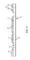
- FIG. 1is a cross-sectional view of a core board sandwiched between two conductive layers of an integrated circuit card according to the preferred embodiment of the present invention
- FIG. 2is a cross-sectional view showing apertures made in the conductive layers shown in FIG. 1 ;
- FIG. 3is a cross-sectional view showing apertures made in the core board shown in FIG. 2 ;
- FIG. 4is a cross-sectional view showing apertures made in a solder resist provided on the core board and one of the conductive layers shown in FIG. 3 ;
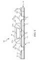
- FIG. 5is a cross-sectional view of metal finishes located in the apertures of the core board and the apertures of the solder resist shown in FIG. 4 ;
- FIG. 6is a cross-sectional view of solder bumps provided on the metal finishes shown in FIG. 5 ;
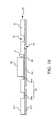
- FIG. 7is a cross-sectional view of a die provided on some of the solder bumps shown in FIG. 6 ;
- FIG. 8is a cross-sectional view of a package provided on the die and a region of the solder resist around the die shown in FIG. 7 ;
- FIG. 9is a cross-sectional view of a substrate of a conventional integrated circuit card
- FIG. 10is a cross-sectional view of a semiconductor die provided on the substrate shown in FIG. 9 ;
- FIG. 11is a cross-sectional view of wires for connecting the substrate to the semiconductor die shown in FIG. 10 ;
- FIG. 12is a cross-sectional view of a package provided on the substrate, semiconductor die and wires shown in FIG. 11 .
- the IC card 100includes a substrate 10 , solder bumps 20 , a semiconductor die 30 and a package 40 .
- the substrate 10is a laminate including a core board 11 and upper and lower metal layers 12 .
- the core board 11includes an upper side 111 and a lower side 112 .
- the upper and lower metal layers 12are preferably made of copper.
- the upper metal layer 12is coated on the upper side 111 of the core board 11 while the lower metal layer 12 is coated on the lower side 112 of the core board 11 .
- the upper metal layer 12is turned into a first conductive layer 12 a by etching for example.
- the lower metal layer 12is turned into a second conductive layer 12 b.
- apertures 13are defined in each of the first and second conductive layers 12 a and 12 b by etching for example. Regions of the upper side 111 of the core board 11 are exposed through the apertures 13 defined in the first conductive layer 12 a . Regions of the lower side 112 of the core board 11 are exposed through the apertures 13 defined in the second conductive layer 12 b.
- apertures 14are defined in the core board 11 by laser drilling for example.
- the upper metal layer 12can be electrically connected to the second conductive layer 12 b through the apertures 14 .
- a solder resist 15is coated on the first conductive layer 12 .
- Apertures 16are defined in the solder resist 15 . Regions of an upper side of the first conductive layer 12 a are exposed via the apertures 16 . Some of the apertures 16 are in communication with some of the apertures 14 . Regions of an upper side of the second conductive layer 12 b are exposed through the aligned apertures 16 and 14 .
- a metal finish 17is coated on each of the regions of the upper side of the first conductive layer 12 a exposed through some of the apertures 16 that are not aligned with the apertures 14 .
- Each of these metal finishes 17is used as a ball pad 17 a .
- a metal finish 17is coated on each of the regions of the upper side of the first conductive layer 12 a exposed through the other apertures 16 .
- a metal finish 17is coated on each of the regions of the upper side of the second conductive layer 12 b exposed through the apertures 14 .
- a metal finish 17(the “lower metal finish 17 ”) is coated on the lower side of the second conductive layer 12 b .
- Aperturesare defined in the lower metal finish 17 corresponding to the apertures 13 defined in the second conductive layer 12 b .
- the metal finishes 17are chemical nickel-gold layers, electroplated nickel-gold layers, immersed silver layers or organic solderability preservative layers (“OSP”) to avoid erosion and deterioration.
- OSPorganic solderability preservative layers
- the solder bumps 20are provided on the ball pads 17 a by printing for example. Some of the solder bumps 20 (the “solder bumps 20 a ”) are filled in some of the apertures 16 that are not aligned with the apertures 14 to cover the ball pads 17 a . Each of the solder bumps 20 a includes a die-mount face 201 a . The other solder bumps 20 (the “solder bumps 20 b ”) are filled in the aligned apertures 16 and 14 .
- the semiconductor die 30is provided on the die-mount faces 201 a of the solder bumps 20 a by adhesive for example.
- the package 40is provided on the die-mount faces 201 a of the solder bumps 20 a and a region of the upper side of the solder resist 15 around the solder bumps 20 a .
- the semiconductor die 30is sealed by the package 40 .
- the IC card 100is made of a laminate according to surface mount technology (“SMT”) instead of wire bonding. Furthermore, there is no need to use electroplating.
- the first conductive layer 12 ais connected to the second conductive 12 b via the solder bumps 20 b .
- cost of the laminateis low, and the throughput of the packaging is high.
- the resultant IC card 100is inexpensive.
Landscapes
- Engineering & Computer Science (AREA)
- Microelectronics & Electronic Packaging (AREA)
- Physics & Mathematics (AREA)
- Condensed Matter Physics & Semiconductors (AREA)
- General Physics & Mathematics (AREA)
- Computer Hardware Design (AREA)
- Power Engineering (AREA)
- Wire Bonding (AREA)
- Production Of Multi-Layered Print Wiring Board (AREA)
Abstract
Description
- 1. Field of Invention
- The present invention relates to an integrated circuit card and, more particularly, to an integrated circuit card made by surface mount technology, not wire bonding.
- 2. Related Prior Art
- Referring to
FIGS. 9 through 12 , there is shown a conventional integrated circuit (“IC”)card 500. TheIC card 500 includes asubstrate 50, asemiconductor die 60,wires 70 and apackage 80. - Referring to
FIG. 9 , thesubstrate 50 is a laminate including acore board 51 and aconductive layer 53. Thecore board 51 includes anupper side 511 and alower side 512.Apertures 52 are defined in thecore board 51. Theconductive layer 53 is coated on thelower side 512 of thecore board 51. Regions of an upper side of theconductive layer 53 are exposed through theapertures 52. Ametal finish 55 is coated on each of these regions of the upper side of theconductive layer 53. One of themetal finishes 55 is used as a die-mount pad 55a. Theother metal finishes 55 are used asbonding pads 55a. Ametal finish 56 is coated on a lower side of theconductive layer 53.Apertures 54 are defined in theconductive layer 53 and themetal finish 56. - Referring to
FIG. 10 , the semiconductor die60 is provided on the die-mount pad 55aviaadhesive 6. - Referring to
FIG. 11 ,ball pads 61 are provided on an active side of the semiconductor die60. Each of theball pads 61 is connected to a related one of thebonding pads 55bthrough a related one of thewires 70. - Referring to
FIG. 12 , thepackage 80 is provided on theupper side 511 of thecore board 51 and thebonding pads 55bto seal thesemiconductor die 60 and thewires 70. Thus, theconventional IC card 500 is made. Thesubstrate 50 is however expensive since it is made in a proprietary process. - To overcome the foregoing problem, there has been developed a process for making another conventional IC card from a laminate instead of the
substrate 50. In the laminate, a circuit provided on a metal layer is connected to a circuit provided on another metal layer by electroplating. Therefore, the laminate is still expensive. - The present invention is therefore intended to obviate or at least alleviate the problems encountered in prior art.
- It is the primary objective of the present invention to provide an inexpensive IC card.
- To achieve the foregoing objective, the integrated circuit card includes a laminate, solder bumps, a semiconductor die and a package. The laminate includes a core board, first and second conductive layers, a solder resist and metal finishes. Apertures are defined in the core board. The first conductive layer is coated on an upper side of the core board and made with apertures. Some of the apertures of the first conductive layer are in communication with the apertures of the core board. The second conductive layer is coated on a lower side of the core board. The solder resist is coated on the first conductive layer and made with apertures in communication with the apertures of the first conductive layer. Some of the metal finishes are coated on regions of the first conductive layer exposed through the apertures of the solder resist. The other metal finishes are coated on regions of the second conductive layer exposed through the apertures of the core board. Some of the solder bumps are provided on the metal finishes located in the apertures of the solder resist that are not in communication with the apertures of the core board, and each of them includes a die-mount face. The other solder bumps are provided on the metal finishes located in the apertures of the solder resist that are in communication with the apertures of the core board and the metal finishes located in the apertures of the core board. The semiconductor die is provided on the die-mount faces. The package is provided on the semiconductor die and a region of the solder resist around the semiconductor die.
- Other objectives, advantages and features of the present invention will be apparent from the following description referring to the attached drawings.
- The present invention will be described via detailed illustration of the preferred embodiment versus prior art referring to the drawings wherein:
FIG. 1 is a cross-sectional view of a core board sandwiched between two conductive layers of an integrated circuit card according to the preferred embodiment of the present invention;FIG. 2 is a cross-sectional view showing apertures made in the conductive layers shown inFIG. 1 ;FIG. 3 is a cross-sectional view showing apertures made in the core board shown inFIG. 2 ;FIG. 4 is a cross-sectional view showing apertures made in a solder resist provided on the core board and one of the conductive layers shown inFIG. 3 ;FIG. 5 is a cross-sectional view of metal finishes located in the apertures of the core board and the apertures of the solder resist shown inFIG. 4 ;FIG. 6 is a cross-sectional view of solder bumps provided on the metal finishes shown inFIG. 5 ;FIG. 7 is a cross-sectional view of a die provided on some of the solder bumps shown inFIG. 6 ;FIG. 8 is a cross-sectional view of a package provided on the die and a region of the solder resist around the die shown inFIG. 7 ;FIG. 9 is a cross-sectional view of a substrate of a conventional integrated circuit card;FIG. 10 is a cross-sectional view of a semiconductor die provided on the substrate shown inFIG. 9 ;FIG. 11 is a cross-sectional view of wires for connecting the substrate to the semiconductor die shown inFIG. 10 ; andFIG. 12 is a cross-sectional view of a package provided on the substrate, semiconductor die and wires shown inFIG. 11 .- Referring to
FIGS. 1 through 8 , there is shown a process for making an integrated circuit (“IC”)card 100 according to the preferred embodiment of the present invention. TheIC card 100 includes asubstrate 10,solder bumps 20, a semiconductor die30 and apackage 40. - Referring to
FIG. 1 , thesubstrate 10 is a laminate including acore board 11 and upper andlower metal layers 12. Thecore board 11 includes anupper side 111 and alower side 112. The upper andlower metal layers 12 are preferably made of copper. Theupper metal layer 12 is coated on theupper side 111 of thecore board 11 while thelower metal layer 12 is coated on thelower side 112 of thecore board 11. Theupper metal layer 12 is turned into a firstconductive layer 12aby etching for example. Similarly, thelower metal layer 12 is turned into a secondconductive layer 12b. - Referring to
FIG. 2 ,apertures 13 are defined in each of the first and secondconductive layers upper side 111 of thecore board 11 are exposed through theapertures 13 defined in the firstconductive layer 12a. Regions of thelower side 112 of thecore board 11 are exposed through theapertures 13 defined in the secondconductive layer 12b. - Referring to
FIG. 3 ,apertures 14 are defined in thecore board 11 by laser drilling for example. Theupper metal layer 12 can be electrically connected to the secondconductive layer 12bthrough theapertures 14. - Referring to
FIG. 4 , a solder resist15 is coated on the firstconductive layer 12.Apertures 16 are defined in the solder resist15. Regions of an upper side of the firstconductive layer 12aare exposed via theapertures 16. Some of theapertures 16 are in communication with some of theapertures 14. Regions of an upper side of the secondconductive layer 12bare exposed through the alignedapertures - Referring to
FIG. 5 , ametal finish 17 is coated on each of the regions of the upper side of the firstconductive layer 12aexposed through some of theapertures 16 that are not aligned with theapertures 14. Each of these metal finishes17 is used as aball pad 17a. Ametal finish 17 is coated on each of the regions of the upper side of the firstconductive layer 12aexposed through theother apertures 16. Ametal finish 17 is coated on each of the regions of the upper side of the secondconductive layer 12bexposed through theapertures 14. A metal finish17 (the “lower metal finish 17”) is coated on the lower side of the secondconductive layer 12b. Apertures are defined in thelower metal finish 17 corresponding to theapertures 13 defined in the secondconductive layer 12b. The metal finishes17 are chemical nickel-gold layers, electroplated nickel-gold layers, immersed silver layers or organic solderability preservative layers (“OSP”) to avoid erosion and deterioration. - Referring to
FIG. 6 , the solder bumps20 are provided on theball pads 17aby printing for example. Some of the solder bumps20 (the “solder bumps20a”) are filled in some of theapertures 16 that are not aligned with theapertures 14 to cover theball pads 17a. Each of the solder bumps20aincludes a die-mount face 201a. The other solder bumps20 (the “solder bumps20b”) are filled in the alignedapertures - Referring to
FIG. 7 , the semiconductor die30 is provided on the die-mount faces201aof the solder bumps20aby adhesive for example. - Referring to
FIG. 8 , thepackage 40 is provided on the die-mount faces201aof the solder bumps20aand a region of the upper side of the solder resist15 around the solder bumps20a. Thus, the semiconductor die30 is sealed by thepackage 40. - Advantageously, the
IC card 100 is made of a laminate according to surface mount technology (“SMT”) instead of wire bonding. Furthermore, there is no need to use electroplating. The firstconductive layer 12ais connected to the second conductive12bvia the solder bumps20b. Thus, cost of the laminate is low, and the throughput of the packaging is high. Hence, theresultant IC card 100 is inexpensive. - The present invention has been described via the detailed illustration of the preferred embodiment. Those skilled in the art can derive variations from the preferred embodiment without departing from the scope of the present invention. Therefore, the preferred embodiment shall not limit the scope of the present invention defined in the claims.
Claims (6)
Applications Claiming Priority (2)
| Application Number | Priority Date | Filing Date | Title |
|---|---|---|---|
| TW99205008 | 2010-03-22 | ||
| TW099205008 | 2010-03-22 |
Publications (2)
| Publication Number | Publication Date |
|---|---|
| US20110228487A1true US20110228487A1 (en) | 2011-09-22 |
| US8416576B2 US8416576B2 (en) | 2013-04-09 |
Family
ID=44647107
Family Applications (1)
| Application Number | Title | Priority Date | Filing Date |
|---|---|---|---|
| US12/796,867Active2031-03-20US8416576B2 (en) | 2010-03-22 | 2010-06-09 | Integrated circuit card |
Country Status (3)
| Country | Link |
|---|---|
| US (1) | US8416576B2 (en) |
| JP (1) | JP3163743U (en) |
| TW (1) | TWM397596U (en) |
Families Citing this family (2)
| Publication number | Priority date | Publication date | Assignee | Title |
|---|---|---|---|---|
| CN108601210A (en)* | 2018-03-16 | 2018-09-28 | 沈雪芳 | Printed circuit board and preparation method thereof |
| US11997799B2 (en)* | 2021-02-05 | 2024-05-28 | Shennan Circuits Co., Ltd. | Method for manufacturing printed circuit board |
Citations (21)
| Publication number | Priority date | Publication date | Assignee | Title |
|---|---|---|---|---|
| US5006673A (en)* | 1989-12-07 | 1991-04-09 | Motorola, Inc. | Fabrication of pad array carriers from a universal interconnect structure |
| US5347159A (en)* | 1990-09-24 | 1994-09-13 | Tessera, Inc. | Semiconductor chip assemblies with face-up mounting and rear-surface connection to substrate |
| US5386341A (en)* | 1993-11-01 | 1995-01-31 | Motorola, Inc. | Flexible substrate folded in a U-shape with a rigidizer plate located in the notch of the U-shape |
| US5780143A (en)* | 1995-03-01 | 1998-07-14 | Tokuyama Corporation | Circuit board |
| US5783870A (en)* | 1995-03-16 | 1998-07-21 | National Semiconductor Corporation | Method for connecting packages of a stacked ball grid array structure |
| US5798564A (en)* | 1995-12-21 | 1998-08-25 | Texas Instruments Incorporated | Multiple chip module apparatus having dual sided substrate |
| US5848467A (en)* | 1990-09-24 | 1998-12-15 | Tessera, Inc. | Methods of making semiconductor chip assemblies |
| US5901041A (en)* | 1997-12-02 | 1999-05-04 | Northern Telecom Limited | Flexible integrated circuit package |
| US5915170A (en)* | 1994-09-20 | 1999-06-22 | Tessera, Inc. | Multiple part compliant interface for packaging of a semiconductor chip and method therefor |
| US6265782B1 (en)* | 1996-10-08 | 2001-07-24 | Hitachi Chemical Co., Ltd. | Semiconductor device, semiconductor chip mounting substrate, methods of manufacturing the device and substrate, adhesive, and adhesive double coated film |
| US6376769B1 (en)* | 1999-05-18 | 2002-04-23 | Amerasia International Technology, Inc. | High-density electronic package, and method for making same |
| US6440542B1 (en)* | 1999-12-08 | 2002-08-27 | Ibiden Co., Ltd. | Copper-clad laminated board, and circuit board for printed wiring board and method for producing the same |
| US6586843B2 (en)* | 2001-11-08 | 2003-07-01 | Intel Corporation | Integrated circuit device with covalently bonded connection structure |
| US20040108600A1 (en)* | 2001-12-28 | 2004-06-10 | Jimmy Liang | Method and apparatus for flip chip device assembly by radiant heating |
| US7154046B2 (en)* | 1999-06-01 | 2006-12-26 | Amerasia International Technology, Inc. | Flexible dielectric electronic substrate and method for making same |
| US20080020503A1 (en)* | 2005-01-20 | 2008-01-24 | Sheats James R | Series interconnected optoelectronic device module assembly |
| US20080224248A1 (en)* | 2007-03-15 | 2008-09-18 | Advanced Chip Engineering Technology Inc. | Image sensor module having build-in package cavity and the method of the same |
| US7484293B2 (en)* | 2005-12-28 | 2009-02-03 | International Business Machines Corporation | Semiconductor package and manufacturing method therefor |
| US20100051341A1 (en)* | 2008-08-27 | 2010-03-04 | Hung-Hsiang Cheng | Circuit substrate having power/ground plane with grid holes |
| US20100096176A1 (en)* | 2001-04-26 | 2010-04-22 | Seung-Taek Lim | Contact structure of a wires and method manufacturing the same, and thin film transistor substrate including the contact structure and method manufacturing the same |
| US20100103634A1 (en)* | 2007-03-30 | 2010-04-29 | Takuo Funaya | Functional-device-embedded circuit board, method for manufacturing the same, and electronic equipment |
- 2010
- 2010-04-15TWTW099206170Upatent/TWM397596U/ennot_activeIP Right Cessation
- 2010-06-09USUS12/796,867patent/US8416576B2/enactiveActive
- 2010-08-19JPJP2010005540Upatent/JP3163743U/ennot_activeExpired - Fee Related
Patent Citations (23)
| Publication number | Priority date | Publication date | Assignee | Title |
|---|---|---|---|---|
| US5006673A (en)* | 1989-12-07 | 1991-04-09 | Motorola, Inc. | Fabrication of pad array carriers from a universal interconnect structure |
| US5950304A (en)* | 1990-09-24 | 1999-09-14 | Tessera, Inc. | Methods of making semiconductor chip assemblies |
| US5347159A (en)* | 1990-09-24 | 1994-09-13 | Tessera, Inc. | Semiconductor chip assemblies with face-up mounting and rear-surface connection to substrate |
| US5848467A (en)* | 1990-09-24 | 1998-12-15 | Tessera, Inc. | Methods of making semiconductor chip assemblies |
| US5386341A (en)* | 1993-11-01 | 1995-01-31 | Motorola, Inc. | Flexible substrate folded in a U-shape with a rigidizer plate located in the notch of the U-shape |
| US5915170A (en)* | 1994-09-20 | 1999-06-22 | Tessera, Inc. | Multiple part compliant interface for packaging of a semiconductor chip and method therefor |
| US5780143A (en)* | 1995-03-01 | 1998-07-14 | Tokuyama Corporation | Circuit board |
| US5783870A (en)* | 1995-03-16 | 1998-07-21 | National Semiconductor Corporation | Method for connecting packages of a stacked ball grid array structure |
| US5798564A (en)* | 1995-12-21 | 1998-08-25 | Texas Instruments Incorporated | Multiple chip module apparatus having dual sided substrate |
| US6265782B1 (en)* | 1996-10-08 | 2001-07-24 | Hitachi Chemical Co., Ltd. | Semiconductor device, semiconductor chip mounting substrate, methods of manufacturing the device and substrate, adhesive, and adhesive double coated film |
| US5901041A (en)* | 1997-12-02 | 1999-05-04 | Northern Telecom Limited | Flexible integrated circuit package |
| US6376769B1 (en)* | 1999-05-18 | 2002-04-23 | Amerasia International Technology, Inc. | High-density electronic package, and method for making same |
| US7154046B2 (en)* | 1999-06-01 | 2006-12-26 | Amerasia International Technology, Inc. | Flexible dielectric electronic substrate and method for making same |
| US6440542B1 (en)* | 1999-12-08 | 2002-08-27 | Ibiden Co., Ltd. | Copper-clad laminated board, and circuit board for printed wiring board and method for producing the same |
| US20100096176A1 (en)* | 2001-04-26 | 2010-04-22 | Seung-Taek Lim | Contact structure of a wires and method manufacturing the same, and thin film transistor substrate including the contact structure and method manufacturing the same |
| US6586843B2 (en)* | 2001-11-08 | 2003-07-01 | Intel Corporation | Integrated circuit device with covalently bonded connection structure |
| US20040108600A1 (en)* | 2001-12-28 | 2004-06-10 | Jimmy Liang | Method and apparatus for flip chip device assembly by radiant heating |
| US20080020503A1 (en)* | 2005-01-20 | 2008-01-24 | Sheats James R | Series interconnected optoelectronic device module assembly |
| US7484293B2 (en)* | 2005-12-28 | 2009-02-03 | International Business Machines Corporation | Semiconductor package and manufacturing method therefor |
| US20090047755A1 (en)* | 2005-12-28 | 2009-02-19 | International Business Machines Corporation | Semiconductor package and manufacturing method therefor |
| US20080224248A1 (en)* | 2007-03-15 | 2008-09-18 | Advanced Chip Engineering Technology Inc. | Image sensor module having build-in package cavity and the method of the same |
| US20100103634A1 (en)* | 2007-03-30 | 2010-04-29 | Takuo Funaya | Functional-device-embedded circuit board, method for manufacturing the same, and electronic equipment |
| US20100051341A1 (en)* | 2008-08-27 | 2010-03-04 | Hung-Hsiang Cheng | Circuit substrate having power/ground plane with grid holes |
Also Published As
| Publication number | Publication date |
|---|---|
| TWM397596U (en) | 2011-02-01 |
| US8416576B2 (en) | 2013-04-09 |
| JP3163743U (en) | 2010-10-28 |
Similar Documents
| Publication | Publication Date | Title |
|---|---|---|
| US7706148B2 (en) | Stack structure of circuit boards embedded with semiconductor chips | |
| US9179549B2 (en) | Packaging substrate having embedded passive component and fabrication method thereof | |
| US20110057323A1 (en) | Packaging structure having embedded semiconductor element and method for fabricating the same | |
| US20070158799A1 (en) | Interconnected IC packages with vertical SMT pads | |
| US20080246135A1 (en) | Stacked package module | |
| US9490221B2 (en) | Semiconductor device having multiple magnetic shield members | |
| JP2009141169A (en) | Semiconductor device | |
| US8008765B2 (en) | Semiconductor package having adhesive layer and method of manufacturing the same | |
| US20150035147A1 (en) | Fine Pitch stud POP Structure and Method | |
| US20060267215A1 (en) | Semiconductor device, semiconductor device mounting board, and method for mounting semiconductor device | |
| US8067698B2 (en) | Wiring substrate for use in semiconductor apparatus, method for fabricating the same, and semiconductor apparatus using the same | |
| US9305912B2 (en) | Stack package and method for manufacturing the same | |
| CN100426496C (en) | Semiconductor device and method for manufacturing the same | |
| US8063313B2 (en) | Printed circuit board and semiconductor package including the same | |
| US6855573B2 (en) | Integrated circuit package and manufacturing method therefor with unique interconnector | |
| US8416576B2 (en) | Integrated circuit card | |
| US9318354B2 (en) | Semiconductor package and fabrication method thereof | |
| US10201086B2 (en) | Electronic device | |
| KR100631997B1 (en) | Stack chip package | |
| JP2016063002A (en) | Semiconductor device and manufacturing method thereof | |
| US20090289358A1 (en) | Semiconductor device, method of manufacturing the same, and substrate | |
| US20090039493A1 (en) | Packaging substrate and application thereof | |
| KR102472045B1 (en) | Semiconductor package | |
| US20150171041A1 (en) | Chip element and chip package | |
| KR20020028473A (en) | Stack package |
Legal Events
| Date | Code | Title | Description |
|---|---|---|---|
| AS | Assignment | Owner name:MAO BANG ELECTRONIC CO., LTD., TAIWAN Free format text:ASSIGNMENT OF ASSIGNORS INTEREST;ASSIGNORS:CHU, TSE MIN;LIANG, JIMMY;REEL/FRAME:024509/0951 Effective date:20100607 | |
| AS | Assignment | Owner name:AFLASH TECHNOLOGY CO., LTD., TAIWAN Free format text:ASSIGNMENT OF ASSIGNORS INTEREST;ASSIGNOR:MAO BANG ELECTRONIC CO., LTD.;REEL/FRAME:026723/0208 Effective date:20110728 | |
| STCF | Information on status: patent grant | Free format text:PATENTED CASE | |
| FPAY | Fee payment | Year of fee payment:4 | |
| FEPP | Fee payment procedure | Free format text:7.5 YR SURCHARGE - LATE PMT W/IN 6 MO, SMALL ENTITY (ORIGINAL EVENT CODE: M2555); ENTITY STATUS OF PATENT OWNER: SMALL ENTITY | |
| MAFP | Maintenance fee payment | Free format text:PAYMENT OF MAINTENANCE FEE, 8TH YR, SMALL ENTITY (ORIGINAL EVENT CODE: M2552); ENTITY STATUS OF PATENT OWNER: SMALL ENTITY Year of fee payment:8 | |
| AS | Assignment | Owner name:XIAMEN MSSB TECHNOLOGY CO., LTD., CHINA Free format text:ASSIGNMENT OF ASSIGNORS INTEREST;ASSIGNOR:AFLASH TECHNOLOGY CO., LTD.;REEL/FRAME:056716/0488 Effective date:20210623 | |
| AS | Assignment | Owner name:TOP BUMPING SEMICONDUCTOR CO., LTD., CHINA Free format text:ASSIGNMENT OF ASSIGNORS INTEREST;ASSIGNOR:XIAMEN MSSB TECHNOLOGY CO., LTD.;REEL/FRAME:064208/0013 Effective date:20230703 | |
| FEPP | Fee payment procedure | Free format text:11.5 YR SURCHARGE- LATE PMT W/IN 6 MO, SMALL ENTITY (ORIGINAL EVENT CODE: M2556); ENTITY STATUS OF PATENT OWNER: SMALL ENTITY | |
| MAFP | Maintenance fee payment | Free format text:PAYMENT OF MAINTENANCE FEE, 12TH YR, SMALL ENTITY (ORIGINAL EVENT CODE: M2553); ENTITY STATUS OF PATENT OWNER: SMALL ENTITY Year of fee payment:12 |