US20110227846A1 - Touch panel and manufacturing method therefor - Google Patents
Touch panel and manufacturing method thereforDownload PDFInfo
- Publication number
- US20110227846A1 US20110227846A1US13/048,092US201113048092AUS2011227846A1US 20110227846 A1US20110227846 A1US 20110227846A1US 201113048092 AUS201113048092 AUS 201113048092AUS 2011227846 A1US2011227846 A1US 2011227846A1
- Authority
- US
- United States
- Prior art keywords
- print layer
- touch panel
- glass cover
- region
- conductive film
- Prior art date
- Legal status (The legal status is an assumption and is not a legal conclusion. Google has not performed a legal analysis and makes no representation as to the accuracy of the status listed.)
- Granted
Links
Images


Classifications
- G—PHYSICS
- G06—COMPUTING OR CALCULATING; COUNTING
- G06F—ELECTRIC DIGITAL DATA PROCESSING
- G06F3/00—Input arrangements for transferring data to be processed into a form capable of being handled by the computer; Output arrangements for transferring data from processing unit to output unit, e.g. interface arrangements
- G06F3/01—Input arrangements or combined input and output arrangements for interaction between user and computer
- G06F3/03—Arrangements for converting the position or the displacement of a member into a coded form
- G06F3/041—Digitisers, e.g. for touch screens or touch pads, characterised by the transducing means
- G06F3/044—Digitisers, e.g. for touch screens or touch pads, characterised by the transducing means by capacitive means
- G06F3/0443—Digitisers, e.g. for touch screens or touch pads, characterised by the transducing means by capacitive means using a single layer of sensing electrodes
- G—PHYSICS
- G06—COMPUTING OR CALCULATING; COUNTING
- G06F—ELECTRIC DIGITAL DATA PROCESSING
- G06F3/00—Input arrangements for transferring data to be processed into a form capable of being handled by the computer; Output arrangements for transferring data from processing unit to output unit, e.g. interface arrangements
- G06F3/01—Input arrangements or combined input and output arrangements for interaction between user and computer
- G06F3/03—Arrangements for converting the position or the displacement of a member into a coded form
- G06F3/041—Digitisers, e.g. for touch screens or touch pads, characterised by the transducing means
- G06F3/044—Digitisers, e.g. for touch screens or touch pads, characterised by the transducing means by capacitive means
- G06F3/0446—Digitisers, e.g. for touch screens or touch pads, characterised by the transducing means by capacitive means using a grid-like structure of electrodes in at least two directions, e.g. using row and column electrodes
- G—PHYSICS
- G06—COMPUTING OR CALCULATING; COUNTING
- G06F—ELECTRIC DIGITAL DATA PROCESSING
- G06F2203/00—Indexing scheme relating to G06F3/00 - G06F3/048
- G06F2203/041—Indexing scheme relating to G06F3/041 - G06F3/045
- G06F2203/04102—Flexible digitiser, i.e. constructional details for allowing the whole digitising part of a device to be flexed or rolled like a sheet of paper
- G—PHYSICS
- G06—COMPUTING OR CALCULATING; COUNTING
- G06F—ELECTRIC DIGITAL DATA PROCESSING
- G06F2203/00—Indexing scheme relating to G06F3/00 - G06F3/048
- G06F2203/041—Indexing scheme relating to G06F3/041 - G06F3/045
- G06F2203/04103—Manufacturing, i.e. details related to manufacturing processes specially suited for touch sensitive devices
- G—PHYSICS
- G06—COMPUTING OR CALCULATING; COUNTING
- G06F—ELECTRIC DIGITAL DATA PROCESSING
- G06F2203/00—Indexing scheme relating to G06F3/00 - G06F3/048
- G06F2203/041—Indexing scheme relating to G06F3/041 - G06F3/045
- G06F2203/04107—Shielding in digitiser, i.e. guard or shielding arrangements, mostly for capacitive touchscreens, e.g. driven shields, driven grounds
- G—PHYSICS
- G06—COMPUTING OR CALCULATING; COUNTING
- G06F—ELECTRIC DIGITAL DATA PROCESSING
- G06F2203/00—Indexing scheme relating to G06F3/00 - G06F3/048
- G06F2203/041—Indexing scheme relating to G06F3/041 - G06F3/045
- G06F2203/04111—Cross over in capacitive digitiser, i.e. details of structures for connecting electrodes of the sensing pattern where the connections cross each other, e.g. bridge structures comprising an insulating layer, or vias through substrate
- G—PHYSICS
- G06—COMPUTING OR CALCULATING; COUNTING
- G06F—ELECTRIC DIGITAL DATA PROCESSING
- G06F2203/00—Indexing scheme relating to G06F3/00 - G06F3/048
- G06F2203/041—Indexing scheme relating to G06F3/041 - G06F3/045
- G06F2203/04112—Electrode mesh in capacitive digitiser: electrode for touch sensing is formed of a mesh of very fine, normally metallic, interconnected lines that are almost invisible to see. This provides a quite large but transparent electrode surface, without need for ITO or similar transparent conductive material
Definitions
- This applicationrelates to a touch panel wherein an input position detecting electrode is formed on a glass cover and a manufacturing method for the touch panel.
- a touch panel of the capacitance typea light transmitting input position detecting electrode is formed on one face of a glass substrate.
- the input position detecting electrodeis formed in an inputting region at a central portion of the glass substrate while a peripheral wiring line is formed at a peripheral position of the glass substrate on the outer side of the inputting region.
- a light transmitting glass coveris adhered to the side of the glass substrate, for which an inputting operation is carried out, by a bonding agent.
- a touch panel of the type describedis disclosed, for example, in Japanese Patent Laid-Open No. 2009-259203.
- a touch panelis configured such that an input position detecting electrode and a peripheral wiring line are formed on a second face of a glass cover opposite to a first face for which an inputting operation is carried out, then a glass substrate separate from the glass cover can be omitted. Therefore, the touch panel of the configuration just described is advantageous in that reduction of the number of parts can be anticipated and reduction in thickness and weight can be anticipated.
- a touch panelis sometimes configured such that, in order to assure a good outward appearance thereof, a colored print layer is provided in a peripheral region of the second face side of the glass cover. Accordingly, it seems a possibly good structure to form a colored print layer on a lower layer side than the peripheral wiring line to hide the mounting portion of the flexible circuit board.
- the colored print layeris first formed on the overall peripheral region including the mounting region, and then the input position detecting electrode in the inputting region and a light transmitting conductor film, which configures the peripheral wiring line, are formed. Therefore, there is a problem that, upon formation of the light transmitting conductor film, the transparency of the light transmitting conductor film is degraded significantly by outgas generated from the colored print layer.
- a touch panelwhich can prevent significant degradation of the transparency of a light transmitting conductor film, which configures an input position detecting electrode, even in the case where a connecting portion of a flexible circuit board to a glass cover is hidden with the print layer on the lower layer side and a manufacturing method for the touch panel.
- a touch panelincluding a glass cover, a light transmitting conductive film formed on a second face side of the glass cover opposite to a first face of an inputting operation face side and configuring an input position detecting electrode in an inputting region and a peripheral wiring line extending in a peripheral region on the outer side with respect to the inputting region to a mounting region, a flexible circuit board electrically connected to an end portion of the peripheral wiring line in the mounting region, a light blocking print layer formed on the second face side of the glass cover in an overlapping relationship with an overlapping region between the flexible circuit board and the glass cover on a lower layer side with respect to the peripheral wiring line, and a colored print layer formed on the second face side of the glass cover in the peripheral region on the upper layer side of the peripheral wiring line.
- a manufacturing method for a touch panelincluding a light transmitting conductive film forming step of forming, on a second face side of a glass cover on the opposite side to a first face of an inputting operation face side, a light transmitting conductive film which configures an input position detecting electrode in an inputting region and a peripheral wiring line extending from a peripheral region on the outer side with respect to the inputting region to a mounting region, a mounting step of connecting a flexible circuit board to the mounting region, a first printing step of forming, prior to the light transmitting conductive film forming step, a light blocking print layer overlapping with an overlapping region between the flexible circuit board and the glass cover, and a second printing step of forming a colored print layer in the peripheral region after the light transmitting conductive film forming step.
- the “upper layer side” and the “lower layer side”are used to signify a positional relationship of a plurality of layers formed on the second face of the glass cover irrespective of the upward or downward direction of the touch panel. Therefore, the “lower layer side” signifies the side nearer to the glass cover, that is, the side formed at a preceding step, and the “upper layer side” signifies the side far from the glass cover, that is, the side to be formed at a succeeding step. Further, the “colored print layer” signifies any print layer other than a transparent print layer.
- the input position detecting electrode and the peripheral wiring lineare formed on the second face side on the opposite side to the first face of the input operation face side of the glass cover, and the structure wherein the input position detecting electrode and the peripheral wiring line are formed on a glass substrate separate from the glass cover is not adopted. Therefore, a glass substrate separate from the glass cover is not required, and consequently, reduction of the number of parts can be achieved and reduction in thickness and weight of the touch panel can be anticipated. Further, while the flexible circuit board is connected to the second face side of the glass cover, the light blocking print layer which overlaps with the overlapping region between the flexible circuit board and the glass cover is formed on the lower layer side with respect to the peripheral wiring line.
- the flexible circuit boardis not visible from the input operation face side, that is, from the first face side, of the glass cover.
- the colored print layeris formed in the peripheral region, the colored print layer is formed on the upper layer side with respect to the peripheral wiring line. Therefore, when the light transmitting conductive film which configures the input position detecting electrode and the peripheral wiring line is to be formed, what is formed on the glass cover is only the light blocking print layer from between the light blocking print layer and the colored print layer. Further, the light blocking print layer is formed in a narrow region which overlaps with the overlapping region between the flexible circuit board and the glass cover.
- the light transmitting conductive layerwhen the light transmitting conductive layer is formed, outgas to be generated from the print layers can be suppressed to the minimum, and consequently, the light transmitting conductive film can be formed so as to have high transparency. Therefore, the presence of the input position detecting electrode does not stand out, and when an image is displayed through the touch panel, the image can be displayed with high quality.
- the light blocking print layerhas a thickness smaller than that of the colored print layer.
- the light blocking print layerhas a thickness smaller than 10 ⁇ m. If the light blocking print layer is formed thin in this manner, then since outgas to be generated from the light blocking print layer when the light transmitting conductive film is to be formed can be suppressed to a small amount, the light transmitting conductive film can be formed with high transparency. Further, although the light blocking print layer is placed on the peripheral wiring line, since the thickness of the light blocking print layer is small, there is an advantage also in that an offset cut or disconnection of the wiring line arising from the light blocking print layer becomes less likely to occur.
- the colored print layerpartially overlaps with the light blocking print layer.
- the entire peripheral regioncan be used as a formation region for the colored print layer or the light blocking print layer. Consequently, since no gap is provided between the colored print layer and the light blocking print layer, the touch panel can be provided with improved outward appearance.
- the touch panelmay be configured such that the colored print layer covers a portion of the flexible circuit board which overlaps with the glass cover.
- the touch panelmay be configured such that the colored print layer partially overlaps with the light blocking print layer without overlapping with the flexible circuit board.
- the glass coveris made of tempered glass.
- reduction in thickness of the glass covercan be achieved. Therefore, the touch panel can be configured with a reduced thickness and weight.
- FIGS. 1A and 1Bare a schematic perspective view and a sectional view, respectively, showing an electro-optical apparatus with an inputting function which includes a touch panel according to an embodiment 1 of the present application;
- FIGS. 2A and 2Bare schematic plan views showing a configuration in plan of different portions of the touch panel of FIGS. 1A and 1B ;
- FIGS. 3A and 3Bare sectional views showing a cross sectional configuration of different portions of the touch panel of FIGS. 1A and 1B ;
- FIGS. 4A to 4E and 5 A to 5 Bare schematic sectional views illustrating different steps of a manufacturing method of the touch panel of FIGS. 1A and 1B ;
- FIGS. 6A and 6Bare schematic sectional views showing a touch panel according to an embodiment 2 of the present application.
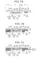
- FIGS. 7A to 7Care schematic sectional views showing a touch panel according to an embodiment 3 of the present application.
- FIGS. 8A to 8Care schematic perspective views showing different electronic equipments which include an electro-optical apparatus with an inputting function to which the present application is applied.
- the side nearer to the glass cover, that is, the side formed at a preceding stepis referred to as “lower face side” while the side far from the glass cover, that is, the side to be formed at a succeeding step, is referred to as “upper face side.”
- FIGS. 1A and 1Bshow an electro-optical apparatus with an inputting function which includes a touch panel according to an embodiment 1 of the present application. More particularly, FIGS. 1A and 1B are a perspective view and a sectional view, respectively, of the electro-optical apparatus with an inputting function.
- the electro-optical apparatus 100 with an inputting function in the present embodimentincludes an image production apparatus 5 which may be configured from a liquid crystal apparatus or the like, and a touch panel 1 disposed in an overlapping relationship on a face of the image production apparatus 5 from which display light is emitted.
- the image production apparatus 5 and the touch panel 1are adhered to each other by a bonding agent layer 85 or the like.
- the image production apparatus 5includes a liquid crystal panel in the form of an electro-optical panel 5 a as a display panel.
- both of the touch panel 1 and the electro-optical panel 5 ahave a rectangular shape in plan, and a central region when the touch panel 1 and the electro-optical apparatus 100 with an inputting function are viewed in plan is an inputting region 2 a . Meanwhile, a region in which the image production apparatus 5 and the electro-optical apparatus 100 with an inputting function overlap with the inputting region 2 a in plan is an image forming region.
- a mounting region 240is provided at an end portion 90 e of the touch panel 1 , and a flexible circuit board 35 is connected at an end portion thereof to the mounting region 240 .
- another flexible circuit board 73is connected at an end portion thereof to the side of the electro-optical panel 5 a on which the end portion 90 e of the touch panel 1 is positioned.
- the image production apparatus 5is an active matrix liquid crystal display apparatus of the transmission type or the semi-transmissive reflection type, and a backlight apparatus not shown is disposed on the opposite side of the electro-optical panel 5 a to the side on which the touch panel 1 is disposed, that is, on the side opposite to the display light emitting side.
- the backlight apparatusincludes, for example, a light transmitting light guide plate disposed in an overlapping relationship on the opposite side of the electro-optical panel 5 a to the side on which the touch panel 1 is disposed, and a light source such as a light emitting diode for emitting white light or the like toward a side end portion of the light guide plate.
- Light emitted from the light sourceis introduced into the side end portion of the light guide plate, propagates in the light guide plate and goes out from the light guide plate toward the electro-optical panel 5 a .
- a sheet-like optical membersuch as a light diffusing sheet or a prism sheet is sometimes interposed.
- a first polarizing plate 81is disposed in an overlapping relationship on the display light emitting side of the electro-optical panel 5 a
- a second polarizing plate 82is disposed in an overlapping relationship on the opposite side of the electro-optical panel 5 a
- the electro-optical panel 5 aincludes a light transmitting element substrate 50 disposed on the opposite side to the display light emitting side thereof, and a light transmitting opposing substrate 60 disposed in an opposing relationship on the element substrate 50 on the display light emitting side.
- the opposing substrate 60 and the element substrate 50are adhered to each other by a seal member 71 of a rectangular framework shape, and a liquid crystal layer 55 is held in a region surrounded by the seal member 71 between the opposing substrate 60 and the element substrate 50 .
- a plurality of pixel electrodes 58are formed from a light transmitting conductive film such as an ITO (Indium Tin Oxide) film or an IZO (Indium Zinc Oxide) film.
- a common electrode 68is formed from a light transmitting conductive film such as an ITO film. Further, a color filter is formed on the opposing substrate 60 .
- the common electrode 68is provided on the element substrate 50 side. Further, the element substrate 50 is sometimes disposed on the display light emitting side of the opposing substrate 60 . In an overhanging portion 59 of the element substrate 50 which overhangs from an edge of the opposing substrate 60 , a driving IC 75 is COG-mounted, and the flexible circuit board 73 is connected to the overhanging portion 59 . It is to be noted that, on the element substrate 50 , a driving circuit is sometimes formed together with switching elements on the element substrate 50 .
- the touch panel 1includes a glass cover 90 on the inputting operation face side thereof.
- the glass cover 90is made of chemically tempered glass.
- Such chemically tempered glassis obtained by immersing glass in molten potassium salt bath of a temperature of approximately 400° C. to carry out a chemically tempering process.
- sodium ionsare exchanged by potassium ions.
- the ion diameter of sodiumis 95 nm
- the ion diameter of potassiumis 133 nm.
- the potassium ionshave a greater ion diameter than the sodium ions. Therefore, the glass substrate is in a state in which the strength thereof is strengthened by the compression stress originating from the chemically tempered film on the surface thereof.
- the glass cover 90 in the present embodimentis approximately 0.2 mm thick and is very thin.
- a light blocking print layer 93On the second face 90 b side of the glass cover 90 positioned on the opposite side to the first face 90 a , although details are hereinafter described, a light blocking print layer 93 , a first light transmitting conductive film 4 a , an interlayer insulating film 23 , a second light transmitting conductive film 4 b and a top coat layer 96 are formed in this order from the lower layer side to the upper layer side. Further, in a peripheral region 2 b , a colored print layer 94 is formed on the upper layer side of the first light transmitting conductive film 4 a , and a region surrounded by the colored print layer 94 makes the inputting region 2 a.
- the first light transmitting conductive film 4 aforms a plurality of input position detecting electrodes 21 in the inputting region 2 a and a plurality of peripheral wiring lines 27 extending from the inputting region 2 a toward the mounting region 240 in the peripheral region 2 b .
- the flexible circuit board 35is connected on the second face 90 b side, and the flexible circuit board 35 is electrically connected to mounting terminals 24 formed from end portions of the peripheral wiring lines 27 .
- a conductive film for shielding formed from a light transmitting film on which a light transmitting conductive film such as an ITO film is formedis sometimes disposed.
- the conductive filmhas a function of preventing a potential variation on the image production apparatus 5 side from having an influence as noise on the input position detecting electrodes 21 . It is to be noted that, in the case where a sufficient distance can be assured between the image production apparatus 5 and the input position detecting electrodes 21 , the conductive film may be omitted.
- FIGS. 2A and 2Bshow a configuration in plan of different portions of the touch panel 1 according to the embodiment 1 of the present application. More particularly, FIG. 2A shows a configuration in plan of the colored print layer 94 and so forth formed on the glass cover 90 , and FIG. 2B shows a configuration in plan of the input position detecting electrodes 21 and so forth formed on the glass cover 90 . It is to be noted that, in FIG. 2B , the inputting region 2 a is indicated by L-shaped marks which individually represent the positions of the four corners thereof.
- a plurality of first electrodes 211 for input position detection extending in an X direction or first direction in the inputting region 2 a and a plurality of second electrodes 212 for input position detection extending in a Y direction or second direction crossing with the X direction in the inputting region 2 aare provided on the second face 90 b side of the glass cover 90 .
- the input position detecting electrodes 21are formed from the first electrodes 211 and the second electrodes 212 .
- peripheral wiring lines 27 extending from one side end portion of the first electrodes 211 and peripheral wiring lines 27 extending from one side end portion of the second electrodes 212are formed in the peripheral region 2 b on the second face 90 b of the glass cover 90 . End portions of the peripheral wiring lines 27 which are positioned in the mounting region 240 configure the mounting terminals 24 .
- FIGS. 3A and 3Bshow a cross sectional configuration of different portions of the touch panel 1 according to the embodiment 1 of the present application. More particularly, FIG. 3A is a cross sectional view of the touch panel 1 taken along line C-C′ of FIG. 2B , and FIG. 3B is a cross sectional view of the touch panel 1 taken along line D-D′ of FIG. 2B .
- the light blocking print layer 93 of a black color, first light transmitting conductive film 4 a , light transmitting interlayer insulating film 23 , second light transmitting conductive film 4 b and top coat layer 96 made of a light transmitting photosensitive resin or the likeare formed in this order from the lower layer side to the upper layer side on the second face 90 b side of the glass cover 90 . Further, in the peripheral region 2 b , the colored print layer 94 of a black color is formed on the upper face side of the first light transmitting conductive film 4 a.
- the first light transmitting conductive film 4 ais formed from a polycrystalline ITO film, and the interlayer insulating film 23 formed from a light transmitting insulating film such as a photosensitive resin film or a silicon oxide film is formed on the upper layer side of the first light transmitting conductive film 4 a .
- the second light transmitting conductive film 4 bis formed from a polycrystalline ITO film similarly to the first light transmitting conductive film 4 a.
- the first light transmitting conductive film 4 ais formed as a plurality of diamond-shaped regions in the inputting region 2 a , and such diamond-shaped regions configure pad portions 211 a and 212 a or large area portions of the input position detecting electrodes 21 , of first electrodes 211 and second electrodes 212 .
- the pad portions 211 a and 212 aare arrayed alternatively in the X direction and the Y direction. Those of the pad portions 211 a which are positioned adjacent each other in the X or first direction are connected to each other through a connecting portion 211 c , and a pad portion 211 a and a connecting portion 211 c configure a first electrode 211 which extends in the X direction.
- pad portions 212 aconfigure second electrodes 212 extending in the Y or second direction
- the interlayer insulating film 23is formed over the overall inputting region 2 a .
- the interlayer insulating film 23has contact holes 23 a formed therein.
- the contact holes 23 aare formed at positions at which they overlap with end portions of the pad portions 212 a opposing through the disconnection portions 218 a .
- the second light transmitting conductive film 4 bis formed as repeating electrodes 215 in a region thereof overlapping with the contact holes 23 a.
- the first electrodes 211 and the second electrodes 212are formed from the same conductive film, that is, from the first light transmitting conductive film 4 a , and besides extend in directions crossing with each other. Therefore, crossing portions 218 at which the first electrodes 211 and the second electrodes 212 cross with each other exist on the glass cover 90 .
- the first electrodes 211 from between the first electrodes 211 and the second electrodes 212extend in a mutually connected relationship in the X direction through the connecting portions 211 c formed from the second light transmitting conductive film 4 b also at the crossing portions 218 .
- the second electrodes 212have the disconnection portions 218 a configured at the crossing portions 218 thereof.
- the repeating electrodes 215are formed in the upper layer of the interlayer insulating film 23 .
- the repeating electrodes 215electrically connect those of the pad portions 212 a , which are adjacent each other with the disconnection portions 218 a interposed therebetween, to each other through the contact holes 23 a of the interlayer insulating film 23 . Therefore, the second electrodes 212 extend in the Y direction in a state in which they are electrically connected to each other in the Y direction. It is to be noted that, since the repeating electrodes 215 overlap with the connecting portions 211 c with the interlayer insulating film 23 interposed therebetween, there is no possibility that they may be short-circuited to each other.
- the peripheral wiring lines 27are formed from the first light transmitting conductive film 4 a on the second face 90 b side of the glass cover 90 , and the input position detecting electrodes 21 , that is, the first electrodes 211 and the second electrodes 212 , and the peripheral wiring lines 27 are electrically connected in a one-by-one corresponding relationship to each other.
- the top coat layer 96made of a photosensitive resin or the like is formed on the upper layer side of the second light transmitting conductive film 4 b .
- the top coat layer 96is formed over the overall area of the inputting region 2 a.
- the peripheral wiring lines 27are formed from the first light transmitting conductive film 4 a similarly to the input position detecting electrodes 21 . Therefore, the peripheral wiring lines 27 cannot be observed from the inputting operation face side, that is, from the first face 90 a side.
- the light blocking print layer 93 of a block coloris formed on the lower layer side with respect to the peripheral wiring line 27 , that is, to the first light transmitting conductive film 4 a side.
- the light blocking print layer 93is formed over a region greater than that of the overlapping region of the flexible circuit board 35 and the glass cover 90 . Therefore, the mounting terminals 24 formed from end portions of the peripheral wiring lines 27 and the flexible circuit board 35 can be electrically connected to each other, and the overlapping portion between the flexible circuit board 35 and the glass cover 90 is not visible as viewed from the inputting operation face side, that is, from the first face 90 a side.
- the touch panel 1is excellent in outward appearance when viewed from the inputting operation face side, that is, from the first face 90 a side.
- the colored print layer 94covers the area in which the flexible circuit board 35 and the glass cover 90 overlap with each other from the opposite side to the side on which the glass cover 90 is positioned, that is, from the upper layer side. Further, the colored print layer 94 overlaps with end portions of the light blocking print layer 93 without interposing the flexible circuit board 35 therebetween.
- the light blocking print layer 93 and the colored print layer 94have the same color, and in the present embodiment, both of the light blocking print layer 93 and the colored print layer 94 are a print layer of a black color. Therefore, although, when the touch panel 1 is viewed from the inputting operation face side, that is, from the first face 90 a side, both of the light blocking print layer 93 and the colored print layer 94 are visible, the light blocking print layer 93 and the colored print layer 94 look as an integral printed region. Therefore, the touch panel 1 is superior in outward appearance when it is viewed from the inputting operation face side, that is, from the first face 90 a side.
- the thickness of the light blocking print layer 93is smaller than that of the colored print layer 94 . More particularly, the thickness of the colored print layer 94 is greater than 10 ⁇ m, for example, is 30 to 50 ⁇ m while the thickness of the light blocking print layer 93 is smaller than 10 ⁇ m.
- the touch panel 1configured in such a manner as described above, if a position detection signal in the form of a rectangular pulse is outputted to an input position detecting electrode 21 , then if no capacitance is parasitic on the input position detecting electrode 21 , then a signal of a waveform same as that of the position detection signal applied to the input position detecting electrode 21 is detected. On the other hand, if a capacitance is parasitic on the input position detecting electrode 21 , then distortion in waveform is caused by the capacitance, and therefore, it can be detected whether or not a capacitance is parasitic on the input position detecting electrode 21 .
- the capacitance at the input position detecting electrode 21 in the proximity of which the finger is positionedincreases by an amount corresponding to the capacitance generated between the input position detecting electrode 21 and the finger. Therefore, the electrode in the proximity of which the finger is positioned can be specified.
- FIGS. 4A to 4E and 5 A and 5 Billustrate a manufacturing method of the touch panel 1 according to the embodiment 1 of the present application. It is to be noted that the left half in FIGS. 4A to 5B corresponds to the sectional view shown in FIG. 3A while the right half corresponds to the sectional view shown in FIG. 3B .
- a glass cover 90 made of optically tempered glassis prepared as seen in FIG. 4A , and then a light blocking print layer 93 of a black color is formed only in a partial region of the second face 90 b side of the glass cover 90 along the end portion 90 e of the glass cover 90 at a first printing step illustrated in FIG. 4B .
- the formation region of the light blocking print layer 93is a region in which a mounting region 240 is to be configured at a later step and which overlaps with an overlapping region between the flexible circuit board 35 and the glass cover 90 .
- the formation region of the light blocking print layer 93is a little greater than the overlapping region between the flexible circuit board 35 and the glass cover 90 , and the thickness of the light blocking print layer 93 is smaller than 10 ⁇ m.
- a film forming step, an patterning step and so forthare carried out repetitively for the second face 90 b side of the glass cover 90 to form a first light transmitting conductive film 4 a , an interlayer insulating film 23 and a second light transmitting conductive film 4 b . More particularly, first at a first light transmitting conductive film forming step illustrated in FIG. 4B , a film forming step and a patterning step of an ITO film are carried out for the second face 90 b of the glass cover 90 to form a first light transmitting conductive film 4 a from which input position detecting electrodes 21 and peripheral wiring lines 27 are to be configured.
- an interlayer insulating film 23 having contact holes 23 a thereinis formed.
- the interlayer insulating film 23is formed from a silicon oxide film
- a film forming step and a patterning step of a silicon oxide filmare carried out, but in the case where the interlayer insulating film 23 is formed from a photosensitive resin, an application step and an exposure and development step of the photosensitive resin are carried out.
- the interlayer insulating film 23is formed over a substantially overall area of the inputting region 2 a but is not formed in the peripheral region 2 b .
- a film forming step and a patterning step of an ITO filmare carried out to form a second light transmitting conductive film 4 b from which repeating electrodes 215 are to be configured.
- a resin application step and a solidification stepare carried out for the second face 90 b side of the glass cover 90 to form a top coat layer 96 .
- the top coat layer 96is formed over an overall area of the inputting region 2 a but is not formed in the peripheral region 2 b.
- a flexible circuit board 35is connected to the mounting region 240 . More particularly, the flexible circuit board 35 has a structure that a conductive layer 351 is formed on an insulating base film 350 , and the conductive layer 351 is electrically connected at end portions thereof to the mounting terminals 24 formed from end portions of the peripheral wiring lines 27 through solder, an anisotropic conductor film, conductive paste or the like.
- a colored print layer 94 of a black coloris formed in the peripheral region 2 b .
- the colored print layer 94is formed such that it covers the portion of the flexible circuit board 35 , which overlaps with the glass cover 90 , on the opposite side to the side on which the glass cover 90 is positioned.
- the thickness of the colored print layer 94is greater than 10 ⁇ m, for example, is 30 to 50 ⁇ m.
- the input position detecting electrodes 21 and the peripheral wiring lines 27are formed on the second face 90 b side of the glass cover 90 opposite to the inputting operation face side, and the structure wherein the input position detecting electrodes 21 and the peripheral wiring lines 27 are formed on a glass substrate separate from the glass cover 90 is not used. Therefore, reduction of the number of parts by omission of the glass substrate can be achieved, and reduction in thickness and weight of the touch panel 1 can be anticipated.
- the flexible circuit board 35is connected to the second face 90 b side of the glass cover 90 , the light blocking print layer 93 which overlaps with the entire overlapping region of the flexible circuit board 35 and the glass cover 90 is formed on the lower layer side of the peripheral wiring line 27 . Therefore, the flexible circuit board 35 is not visible from the inputting operation face side, that is, from the first face 90 a side, of the glass cover 90 , and consequently, the touch panel 1 is good in outward appearance.
- the colored print layer 94is formed in the peripheral region 2 b , the colored print layer 94 is formed on the upper layer side of the peripheral wiring line 27 . Therefore, when the first light transmitting conductive film 4 a which configures the input position detecting electrodes 21 and the peripheral wiring lines 27 is formed, what is formed on the glass cover 90 is only the light blocking print layer 93 from between the light blocking print layer 93 and the colored print layer 94 . Further, the light blocking print layer 93 is formed at a narrow portion which overlaps with the overlapping region between the flexible circuit board 35 and the glass cover 90 .
- the first light transmitting conductive film 4 awhen the first light transmitting conductive film 4 a is formed, outgas to be generated from the print layer can be suppressed to the minimum, and consequently, the first light transmitting conductive film 4 a can be formed with high transparency. More particularly, when the first light transmitting conductive film 4 a in the form of an ITO film is to be formed, in the case where no print layer exists at all, the transmission factor of the first light transmitting conductive film 4 a is equal to or higher than 92%. However, if the print layer exists over the overall area of the peripheral region 2 b , then the transmission factor of the first light transmitting conductive film 4 a drops to 86 to 88%.
- the transmission factor of the first light transmitting conductive film 4 ais 89 to 91%. Therefore, the presence of the input position detecting electrodes 21 does not stand out, and when an image is to be displayed through the touch panel 1 , it can be displayed with high quality.
- the thickness of the light blocking print layer 93is smaller than that of the colored print layer 94 and smaller than 10 ⁇ m. Therefore, when the first light transmitting conductive film 4 a is to be formed, outgas to be generated from the light blocking print layer 93 can be suppressed to a small amount, and consequently, the first light transmitting conductive film 4 a of a high transmission factor can be formed. Further, while the peripheral wiring lines 27 are swollen from the light blocking print layer 93 , since the thickness of the light blocking print layer 93 is small, there is an advantage that an offset cut or disconnection of wiring lines arising from the light blocking print layer 93 becomes less likely to occur.
- the entire inputting region 2 acan be used as a formation region for the colored print layer 94 or the light blocking print layer 93 , and a gap is not generated between the colored print layer 94 and the light blocking print layer 93 . Therefore, the outward appearance of the touch panel 1 can be improved.
- the colored print layer 94covers a portion of the flexible circuit board 35 which overlaps with the glass cover 90 , and the colored print layer 94 is formed after the flexible circuit board 35 is mounted. Therefore, there is no possibility that the colored print layer 94 may be deteriorated by heat when the flexible circuit board 35 is mounted.
- the glass cover 90is formed from tempered glass, the thickness of the glass cover 90 can be reduced to approximately 0.2 mm. Therefore, the touch panel can be configured with a reduced thickness and weight.
- FIGS. 6A and 6Bshow a touch panel 1 according to an embodiment 2 of the present application. It is to be noted that, since a basic configuration of the touch panel 1 of the present embodiment is similar to that of the touch panel 1 of the embodiment 1, like elements are denoted by like reference characters and overlapping description of them is omitted herein to avoid redundancy.
- the colored print layer 94covers the entire region of the flexible circuit board 35 which overlaps with the glass cover 90
- a different configurationmay be adopted wherein the colored print layer 94 overlaps but partially with the light blocking print layer 93 without overlapping with the flexible circuit board 35 .
- a colored print layer 94is formed in such a manner as to partially overlap with the light blocking print layer 93 without overlapping with the flexible circuit board 35 . Also in the case where such a configuration as just described is adopted, substantially similar effects to those by the embodiment 1 can be anticipated.
- FIGS. 7A to 7Cshow a touch panel 1 according to an embodiment 3 of the present application. It is to be noted that, since a basic configuration of the touch panel 1 of the present embodiment is similar to that of the touch panel 1 of the embodiment 1, like elements are denoted by like reference characters and overlapping description of them is omitted herein to avoid redundancy.
- the flexible circuit board 35may be mounted on the glass cover 90 after the colored print layer 94 is formed. More particularly, at the second printing step illustrated in FIG. 7B after the top coat layer forming step illustrated in FIG. 7A , the colored print layer 94 is formed in such a manner as to overlap with an end portion of the light blocking print layer 93 . Then, at the mounting step illustrated in FIG. 7C , the flexible circuit board 35 is mounted on the glass cover 90 . Also in the case where such a configuration as just described is adopted, substantially similar effects to those by the embodiment 1 can be anticipated.
- the input position detecting electrodes 21 and the peripheral wiring lines 27are configured from a common light transmitting conductive film, that is, from the first light transmitting conductive film 4 a made of ITO
- the input position detecting electrodes 21may be configured from the first light transmitting conductive film 4 a of ITO while the peripheral wiring lines 27 may be a separate light transmitting conductive film made of, for example, IZO.
- the input position detecting electrodes 21may be configured from the first light transmitting conductive film 4 a of ITO while the peripheral wiring lines 27 may be a light transmitting conductive film formed from a multilayer film of IZO/Au (gold)/IZO or a light transmitting conductive film formed from a multilayer film of ITO/Au (gold)/ITO.
- Such multilayer filmscan reduce the wiring line resistance of the peripheral wiring lines 27 .
- the input position detecting electrodes 21are formed from the first light transmitting conductive film 4 a and the repeating electrodes 215 are formed from the second light transmitting conductive film 4 b
- the present applicationmay be applied to a different touch panel wherein the repeating electrodes 215 are formed from the first light transmitting conductive film 4 a and the input position detecting electrodes 21 are formed from the second light transmitting conductive film 4 b.
- a liquid crystal apparatusis used as the image production apparatus 5
- an organic electroluminescence apparatusmay be used as the image production apparatus 5 .
- FIGS. 8A to 8Cshow electronic equipments which include the electro-optical apparatus 100 with an inputting function to which the present application is applied.
- FIG. 8Ashows a configuration of a personal computer of the mobile type which includes the electro-optical apparatus 100 with an inputting function.
- the personal computer 2000 shownincludes an electro-optical apparatus 100 with an inputting function as a display unit and a main body section 2010 .
- the main body section 2010includes a power supply switch 2001 and a keyboard 2002 .
- FIG. 8Bshows a configuration of a portable telephone set which includes an electro-optical apparatus 100 with an inputting function.
- the portable telephone set 3000includes a plurality of operation buttons 3001 , a scroll button 3002 , and an electro-optical apparatus 100 with an inputting function as a display unit. If the scroll button 3002 is operated, then a screen image displayed on the electro-optical apparatus 100 with an inputting function is scrolled.
- FIG. 8Cshows a configuration of a personal digital assistant (PDA) to which the electro-optical apparatus 100 with an inputting function is applied.
- the personal digital assistant 4000includes a plurality of operation buttons 4001 , a power supply switch 4002 and an electro-optical apparatus 100 with an inputting function as a display nit. If the power supply switch 4002 is operated, then various kinds of information such as an address book, a schedule table and so forth are displayed on the electro-optical apparatus 100 with an inputting function.
- the electro-optical apparatus 100 with an inputting functioncan be applied not only to the electronic equipments described above with reference to FIGS. 8A to 8C but also to various other electronic equipments including a digital still camera, a liquid crystal television set, a video tape recorder of the viewfinder type or the monitor direct-view type, a car navigation apparatus, a pager, an electronic notebook, a desk-top calculator, a word processor, a work station, a visual telephone set, a POS terminal and a bank terminal.
- the electro-optical apparatus 100 with an inputting function described abovecan be applied as a display section of such various electronic equipments.
Landscapes
- Engineering & Computer Science (AREA)
- General Engineering & Computer Science (AREA)
- Theoretical Computer Science (AREA)
- Human Computer Interaction (AREA)
- Physics & Mathematics (AREA)
- General Physics & Mathematics (AREA)
- Position Input By Displaying (AREA)
- User Interface Of Digital Computer (AREA)
- Microelectronics & Electronic Packaging (AREA)
- Computer Networks & Wireless Communication (AREA)
Abstract
Description
- The present application claims priority to Japanese Priority Patent Application JP 2010-060319 filed in the Japan Patent Office on Mar. 17, 2010, the entire content of which is hereby incorporated by reference.
- This application relates to a touch panel wherein an input position detecting electrode is formed on a glass cover and a manufacturing method for the touch panel.
- While various types of touch panels are known, for example, in a touch panel of the capacitance type, a light transmitting input position detecting electrode is formed on one face of a glass substrate. The input position detecting electrode is formed in an inputting region at a central portion of the glass substrate while a peripheral wiring line is formed at a peripheral position of the glass substrate on the outer side of the inputting region. Further, in the touch panel of the capacitance type, a light transmitting glass cover is adhered to the side of the glass substrate, for which an inputting operation is carried out, by a bonding agent. A touch panel of the type described is disclosed, for example, in Japanese Patent Laid-Open No. 2009-259203.
- If a touch panel is configured such that an input position detecting electrode and a peripheral wiring line are formed on a second face of a glass cover opposite to a first face for which an inputting operation is carried out, then a glass substrate separate from the glass cover can be omitted. Therefore, the touch panel of the configuration just described is advantageous in that reduction of the number of parts can be anticipated and reduction in thickness and weight can be anticipated.
- However, in the case where the peripheral wiring line is formed on the second face of the glass cover, a flexible circuit board is connected to the second face side of the glass cover. Therefore, when the touch panel is viewed from the input operation face, that is, from the first face, of the glass cover, a connecting portion of the flexible circuit board is visible, and there is a problem that the outward appearance of the touch panel is deteriorated significantly.
- Meanwhile, a touch panel is sometimes configured such that, in order to assure a good outward appearance thereof, a colored print layer is provided in a peripheral region of the second face side of the glass cover. Accordingly, it seems a possibly good structure to form a colored print layer on a lower layer side than the peripheral wiring line to hide the mounting portion of the flexible circuit board. However, in order to provide a colored print layer on the lower layer side than the peripheral wiring line on the glass cover, the colored print layer is first formed on the overall peripheral region including the mounting region, and then the input position detecting electrode in the inputting region and a light transmitting conductor film, which configures the peripheral wiring line, are formed. Therefore, there is a problem that, upon formation of the light transmitting conductor film, the transparency of the light transmitting conductor film is degraded significantly by outgas generated from the colored print layer.
- Therefore, it is desirable to provide a touch panel which can prevent significant degradation of the transparency of a light transmitting conductor film, which configures an input position detecting electrode, even in the case where a connecting portion of a flexible circuit board to a glass cover is hidden with the print layer on the lower layer side and a manufacturing method for the touch panel.
- According to an embodiment, there is provided a touch panel including a glass cover, a light transmitting conductive film formed on a second face side of the glass cover opposite to a first face of an inputting operation face side and configuring an input position detecting electrode in an inputting region and a peripheral wiring line extending in a peripheral region on the outer side with respect to the inputting region to a mounting region, a flexible circuit board electrically connected to an end portion of the peripheral wiring line in the mounting region, a light blocking print layer formed on the second face side of the glass cover in an overlapping relationship with an overlapping region between the flexible circuit board and the glass cover on a lower layer side with respect to the peripheral wiring line, and a colored print layer formed on the second face side of the glass cover in the peripheral region on the upper layer side of the peripheral wiring line.
- According to another embodiment, there is provided a manufacturing method for a touch panel, including a light transmitting conductive film forming step of forming, on a second face side of a glass cover on the opposite side to a first face of an inputting operation face side, a light transmitting conductive film which configures an input position detecting electrode in an inputting region and a peripheral wiring line extending from a peripheral region on the outer side with respect to the inputting region to a mounting region, a mounting step of connecting a flexible circuit board to the mounting region, a first printing step of forming, prior to the light transmitting conductive film forming step, a light blocking print layer overlapping with an overlapping region between the flexible circuit board and the glass cover, and a second printing step of forming a colored print layer in the peripheral region after the light transmitting conductive film forming step.
- In the touch panel and the manufacturing method for a touch panel, the “upper layer side” and the “lower layer side” are used to signify a positional relationship of a plurality of layers formed on the second face of the glass cover irrespective of the upward or downward direction of the touch panel. Therefore, the “lower layer side” signifies the side nearer to the glass cover, that is, the side formed at a preceding step, and the “upper layer side” signifies the side far from the glass cover, that is, the side to be formed at a succeeding step. Further, the “colored print layer” signifies any print layer other than a transparent print layer.
- In the present application, the input position detecting electrode and the peripheral wiring line are formed on the second face side on the opposite side to the first face of the input operation face side of the glass cover, and the structure wherein the input position detecting electrode and the peripheral wiring line are formed on a glass substrate separate from the glass cover is not adopted. Therefore, a glass substrate separate from the glass cover is not required, and consequently, reduction of the number of parts can be achieved and reduction in thickness and weight of the touch panel can be anticipated. Further, while the flexible circuit board is connected to the second face side of the glass cover, the light blocking print layer which overlaps with the overlapping region between the flexible circuit board and the glass cover is formed on the lower layer side with respect to the peripheral wiring line. Therefore, the flexible circuit board is not visible from the input operation face side, that is, from the first face side, of the glass cover. Further, while, on the second face side of the glass cover, the colored print layer is formed in the peripheral region, the colored print layer is formed on the upper layer side with respect to the peripheral wiring line. Therefore, when the light transmitting conductive film which configures the input position detecting electrode and the peripheral wiring line is to be formed, what is formed on the glass cover is only the light blocking print layer from between the light blocking print layer and the colored print layer. Further, the light blocking print layer is formed in a narrow region which overlaps with the overlapping region between the flexible circuit board and the glass cover. Therefore, when the light transmitting conductive layer is formed, outgas to be generated from the print layers can be suppressed to the minimum, and consequently, the light transmitting conductive film can be formed so as to have high transparency. Therefore, the presence of the input position detecting electrode does not stand out, and when an image is displayed through the touch panel, the image can be displayed with high quality.
- Preferably, the light blocking print layer has a thickness smaller than that of the colored print layer. Or preferably, the light blocking print layer has a thickness smaller than 10 μm. If the light blocking print layer is formed thin in this manner, then since outgas to be generated from the light blocking print layer when the light transmitting conductive film is to be formed can be suppressed to a small amount, the light transmitting conductive film can be formed with high transparency. Further, although the light blocking print layer is placed on the peripheral wiring line, since the thickness of the light blocking print layer is small, there is an advantage also in that an offset cut or disconnection of the wiring line arising from the light blocking print layer becomes less likely to occur.
- Preferably, the colored print layer partially overlaps with the light blocking print layer. In the case where the touch panel is configured in this manner, the entire peripheral region can be used as a formation region for the colored print layer or the light blocking print layer. Consequently, since no gap is provided between the colored print layer and the light blocking print layer, the touch panel can be provided with improved outward appearance.
- In this instance, the touch panel may be configured such that the colored print layer covers a portion of the flexible circuit board which overlaps with the glass cover.
- Or, the touch panel may be configured such that the colored print layer partially overlaps with the light blocking print layer without overlapping with the flexible circuit board.
- Preferably, the glass cover is made of tempered glass. With the configuration just described, reduction in thickness of the glass cover can be achieved. Therefore, the touch panel can be configured with a reduced thickness and weight.
- Additional features and advantages are described herein, and will be apparent from the following Detailed Description and the figures.
FIGS. 1A and 1B are a schematic perspective view and a sectional view, respectively, showing an electro-optical apparatus with an inputting function which includes a touch panel according to anembodiment 1 of the present application;FIGS. 2A and 2B are schematic plan views showing a configuration in plan of different portions of the touch panel ofFIGS. 1A and 1B ;FIGS. 3A and 3B are sectional views showing a cross sectional configuration of different portions of the touch panel ofFIGS. 1A and 1B ;FIGS. 4A to 4E and5A to5B are schematic sectional views illustrating different steps of a manufacturing method of the touch panel ofFIGS. 1A and 1B ;FIGS. 6A and 6B are schematic sectional views showing a touch panel according to anembodiment 2 of the present application;FIGS. 7A to 7C are schematic sectional views showing a touch panel according to an embodiment 3 of the present application; andFIGS. 8A to 8C are schematic perspective views showing different electronic equipments which include an electro-optical apparatus with an inputting function to which the present application is applied.- Embodiments of the present application will be described below in detail with reference to the drawings.
- In the following, preferred embodiments of the present application are described with reference to the accompanying drawings. It is to be noted that, in the figures referred to in the following description, in order to show various layers and members in respective sizes with which they can be recognized on the drawings, the scales of them are suitably made different from each other. Further, in
FIGS. 1A ,1B and3A to5B referred in the following description, the inputting operation face side is directed upwardly in order to facilitate correspondence among the figures. Therefore, the glass cover is shown such that the second face thereof is directed downwardly. However, in the description given hereinbelow of a positional relationship among a plurality of layers formed on the second face of the glass cover, the side nearer to the glass cover, that is, the side formed at a preceding step, is referred to as “lower face side” while the side far from the glass cover, that is, the side to be formed at a succeeding step, is referred to as “upper face side.” FIGS. 1A and 1B show an electro-optical apparatus with an inputting function which includes a touch panel according to anembodiment 1 of the present application. More particularly,FIGS. 1A and 1B are a perspective view and a sectional view, respectively, of the electro-optical apparatus with an inputting function.- Referring to
FIGS. 1A and 1B , the electro-optical apparatus 100 with an inputting function in the present embodiment includes animage production apparatus 5 which may be configured from a liquid crystal apparatus or the like, and atouch panel 1 disposed in an overlapping relationship on a face of theimage production apparatus 5 from which display light is emitted. Theimage production apparatus 5 and thetouch panel 1 are adhered to each other by abonding agent layer 85 or the like. Theimage production apparatus 5 includes a liquid crystal panel in the form of an electro-optical panel 5aas a display panel. In the present embodiment, both of thetouch panel 1 and the electro-optical panel 5ahave a rectangular shape in plan, and a central region when thetouch panel 1 and the electro-optical apparatus 100 with an inputting function are viewed in plan is an inputtingregion 2a. Meanwhile, a region in which theimage production apparatus 5 and the electro-optical apparatus 100 with an inputting function overlap with the inputtingregion 2ain plan is an image forming region. A mountingregion 240 is provided at anend portion 90eof thetouch panel 1, and aflexible circuit board 35 is connected at an end portion thereof to the mountingregion 240. Meanwhile, anotherflexible circuit board 73 is connected at an end portion thereof to the side of the electro-optical panel 5aon which theend portion 90eof thetouch panel 1 is positioned. - The
image production apparatus 5 is an active matrix liquid crystal display apparatus of the transmission type or the semi-transmissive reflection type, and a backlight apparatus not shown is disposed on the opposite side of the electro-optical panel 5ato the side on which thetouch panel 1 is disposed, that is, on the side opposite to the display light emitting side. The backlight apparatus includes, for example, a light transmitting light guide plate disposed in an overlapping relationship on the opposite side of the electro-optical panel 5ato the side on which thetouch panel 1 is disposed, and a light source such as a light emitting diode for emitting white light or the like toward a side end portion of the light guide plate. Light emitted from the light source is introduced into the side end portion of the light guide plate, propagates in the light guide plate and goes out from the light guide plate toward the electro-optical panel 5a. Between the light guide plate and the electro-optical panel 5a, a sheet-like optical member such as a light diffusing sheet or a prism sheet is sometimes interposed. - In the
image production apparatus 5, a firstpolarizing plate 81 is disposed in an overlapping relationship on the display light emitting side of the electro-optical panel 5a, and a secondpolarizing plate 82 is disposed in an overlapping relationship on the opposite side of the electro-optical panel 5a. The electro-optical panel 5aincludes a lighttransmitting element substrate 50 disposed on the opposite side to the display light emitting side thereof, and a lighttransmitting opposing substrate 60 disposed in an opposing relationship on theelement substrate 50 on the display light emitting side. The opposingsubstrate 60 and theelement substrate 50 are adhered to each other by aseal member 71 of a rectangular framework shape, and aliquid crystal layer 55 is held in a region surrounded by theseal member 71 between the opposingsubstrate 60 and theelement substrate 50. On the face of theelement substrate 50 opposing to the opposingsubstrate 60, a plurality ofpixel electrodes 58 are formed from a light transmitting conductive film such as an ITO (Indium Tin Oxide) film or an IZO (Indium Zinc Oxide) film. On the face of the opposingsubstrate 60 opposing to theelement substrate 50, acommon electrode 68 is formed from a light transmitting conductive film such as an ITO film. Further, a color filter is formed on the opposingsubstrate 60. It is to be noted that, in the case where theimage production apparatus 5 is of the IPS (In Plane Switching) type or the FFS (Fringe Field Switching) type, thecommon electrode 68 is provided on theelement substrate 50 side. Further, theelement substrate 50 is sometimes disposed on the display light emitting side of the opposingsubstrate 60. In an overhangingportion 59 of theelement substrate 50 which overhangs from an edge of the opposingsubstrate 60, a drivingIC 75 is COG-mounted, and theflexible circuit board 73 is connected to the overhangingportion 59. It is to be noted that, on theelement substrate 50, a driving circuit is sometimes formed together with switching elements on theelement substrate 50. - General Configuration of the
Touch Panel 1 - The
touch panel 1 includes aglass cover 90 on the inputting operation face side thereof. In the present embodiment, theglass cover 90 is made of chemically tempered glass. Such chemically tempered glass is obtained by immersing glass in molten potassium salt bath of a temperature of approximately 400° C. to carry out a chemically tempering process. In the chemically tempered glass, sodium ions are exchanged by potassium ions. Here, while the ion diameter of sodium is 95 nm, the ion diameter of potassium is 133 nm. Thus, the potassium ions have a greater ion diameter than the sodium ions. Therefore, the glass substrate is in a state in which the strength thereof is strengthened by the compression stress originating from the chemically tempered film on the surface thereof. Accordingly, theglass cover 90 in the present embodiment is approximately 0.2 mm thick and is very thin. - As seen in
FIG. 1B , on thesecond face 90bside of theglass cover 90 positioned on the opposite side to thefirst face 90a, although details are hereinafter described, a light blockingprint layer 93, a first light transmittingconductive film 4a, aninterlayer insulating film 23, a second light transmittingconductive film 4band atop coat layer 96 are formed in this order from the lower layer side to the upper layer side. Further, in aperipheral region 2b, acolored print layer 94 is formed on the upper layer side of the first light transmittingconductive film 4a, and a region surrounded by thecolored print layer 94 makes the inputtingregion 2a. - In the
touch panel 1 configured in such a manner as described above, from between the first light transmittingconductive film 4aand the second light transmittingconductive film 4b, the first light transmittingconductive film 4aforms a plurality of inputposition detecting electrodes 21 in the inputtingregion 2aand a plurality ofperipheral wiring lines 27 extending from the inputtingregion 2atoward the mountingregion 240 in theperipheral region 2b. Further, to theend portion 90efrom amongend portions glass cover 90, theflexible circuit board 35 is connected on thesecond face 90bside, and theflexible circuit board 35 is electrically connected to mountingterminals 24 formed from end portions of the peripheral wiring lines27. - Between the
touch panel 1 and the electro-optical panel 5a, a conductive film for shielding formed from a light transmitting film on which a light transmitting conductive film such as an ITO film is formed is sometimes disposed. The conductive film has a function of preventing a potential variation on theimage production apparatus 5 side from having an influence as noise on the inputposition detecting electrodes 21. It is to be noted that, in the case where a sufficient distance can be assured between theimage production apparatus 5 and the inputposition detecting electrodes 21, the conductive film may be omitted. - Configuration in Plan of the
Touch Panel 1 FIGS. 2A and 2B show a configuration in plan of different portions of thetouch panel 1 according to theembodiment 1 of the present application. More particularly,FIG. 2A shows a configuration in plan of thecolored print layer 94 and so forth formed on theglass cover 90, andFIG. 2B shows a configuration in plan of the inputposition detecting electrodes 21 and so forth formed on theglass cover 90. It is to be noted that, inFIG. 2B , the inputtingregion 2ais indicated by L-shaped marks which individually represent the positions of the four corners thereof.- Referring to
FIGS. 2A and 2B , in thetouch panel 1 of the present embodiment, a plurality of first electrodes211 for input position detection extending in an X direction or first direction in the inputtingregion 2aand a plurality of second electrodes212 for input position detection extending in a Y direction or second direction crossing with the X direction in the inputtingregion 2aare provided on thesecond face 90bside of theglass cover 90. The inputposition detecting electrodes 21 are formed from the first electrodes211 and the second electrodes212. Meanwhile,peripheral wiring lines 27 extending from one side end portion of the first electrodes211 andperipheral wiring lines 27 extending from one side end portion of the second electrodes212 are formed in theperipheral region 2bon thesecond face 90bof theglass cover 90. End portions of theperipheral wiring lines 27 which are positioned in the mountingregion 240 configure the mountingterminals 24. - Cross Sectional Structure of the
Touch Panel 1 FIGS. 3A and 3B show a cross sectional configuration of different portions of thetouch panel 1 according to theembodiment 1 of the present application. More particularly,FIG. 3A is a cross sectional view of thetouch panel 1 taken along line C-C′ ofFIG. 2B , andFIG. 3B is a cross sectional view of thetouch panel 1 taken along line D-D′ ofFIG. 2B .- Referring to
FIGS. 2A ,2B,3A and3B, the light blockingprint layer 93 of a black color, first light transmittingconductive film 4a, light transmittinginterlayer insulating film 23, second light transmittingconductive film 4bandtop coat layer 96 made of a light transmitting photosensitive resin or the like are formed in this order from the lower layer side to the upper layer side on thesecond face 90bside of theglass cover 90. Further, in theperipheral region 2b, thecolored print layer 94 of a black color is formed on the upper face side of the first light transmittingconductive film 4a. - The first light transmitting
conductive film 4ais formed from a polycrystalline ITO film, and theinterlayer insulating film 23 formed from a light transmitting insulating film such as a photosensitive resin film or a silicon oxide film is formed on the upper layer side of the first light transmittingconductive film 4a. In the present embodiment, also the second light transmittingconductive film 4bis formed from a polycrystalline ITO film similarly to the first light transmittingconductive film 4a. - The first light transmitting
conductive film 4ais formed as a plurality of diamond-shaped regions in the inputtingregion 2a, and such diamond-shaped regions configurepad portions position detecting electrodes 21, of first electrodes211 and second electrodes212. Thepad portions pad portions 211awhich are positioned adjacent each other in the X or first direction are connected to each other through a connectingportion 211c, and apad portion 211aand a connectingportion 211cconfigure a first electrode211 which extends in the X direction. In contrast, while thepad portions 212aconfigure second electrodes212 extending in the Y or second direction, those of thepad portions 212awhich are positioned adjacent each other in the Y direction, that is, portions overlapping with the connectingportions 211cform disconnection portions 218a. - The
interlayer insulating film 23 is formed over theoverall inputting region 2a. Theinterlayer insulating film 23 has contact holes23aformed therein. The contact holes23aare formed at positions at which they overlap with end portions of thepad portions 212aopposing through thedisconnection portions 218a. On the upper layer side of theinterlayer insulating film 23, the second light transmittingconductive film 4bis formed as repeatingelectrodes 215 in a region thereof overlapping with the contact holes23a. - In the
touch panel 1 configured in such a manner as described above, the first electrodes211 and the second electrodes212 are formed from the same conductive film, that is, from the first light transmittingconductive film 4a, and besides extend in directions crossing with each other. Therefore, crossingportions 218 at which the first electrodes211 and the second electrodes212 cross with each other exist on theglass cover 90. Here, the first electrodes211 from between the first electrodes211 and the second electrodes212 extend in a mutually connected relationship in the X direction through the connectingportions 211cformed from the second light transmittingconductive film 4balso at the crossingportions 218. In contrast, the second electrodes212 have thedisconnection portions 218aconfigured at the crossingportions 218 thereof. However, at the crossingportions 218, the repeatingelectrodes 215 are formed in the upper layer of theinterlayer insulating film 23. The repeatingelectrodes 215 electrically connect those of thepad portions 212a, which are adjacent each other with thedisconnection portions 218ainterposed therebetween, to each other through the contact holes23aof theinterlayer insulating film 23. Therefore, the second electrodes212 extend in the Y direction in a state in which they are electrically connected to each other in the Y direction. It is to be noted that, since the repeatingelectrodes 215 overlap with the connectingportions 211cwith theinterlayer insulating film 23 interposed therebetween, there is no possibility that they may be short-circuited to each other. - In the present embodiment, the
peripheral wiring lines 27 are formed from the first light transmittingconductive film 4aon thesecond face 90bside of theglass cover 90, and the inputposition detecting electrodes 21, that is, the first electrodes211 and the second electrodes212, and theperipheral wiring lines 27 are electrically connected in a one-by-one corresponding relationship to each other. - In the present embodiment, on the
second face 90bside of theglass cover 90, thetop coat layer 96 made of a photosensitive resin or the like is formed on the upper layer side of the second light transmittingconductive film 4b. Thetop coat layer 96 is formed over the overall area of the inputtingregion 2a. - Configuration of the Light
Blocking Print Layer 93 and theColored Print Layer 94 - In the
touch panel 1 of the present embodiment, theperipheral wiring lines 27 are formed from the first light transmittingconductive film 4asimilarly to the inputposition detecting electrodes 21. Therefore, theperipheral wiring lines 27 cannot be observed from the inputting operation face side, that is, from thefirst face 90aside. - In a region of the
second face 90bside of theglass cover 90 which overlaps with the overlapping region of theflexible circuit board 35 and theglass cover 90, the light blockingprint layer 93 of a block color is formed on the lower layer side with respect to theperipheral wiring line 27, that is, to the first light transmittingconductive film 4aside. The lightblocking print layer 93 is formed over a region greater than that of the overlapping region of theflexible circuit board 35 and theglass cover 90. Therefore, the mountingterminals 24 formed from end portions of theperipheral wiring lines 27 and theflexible circuit board 35 can be electrically connected to each other, and the overlapping portion between theflexible circuit board 35 and theglass cover 90 is not visible as viewed from the inputting operation face side, that is, from thefirst face 90aside. - Further, since the
colored print layer 94 of a black color is formed in theperipheral region 2b, thetouch panel 1 is excellent in outward appearance when viewed from the inputting operation face side, that is, from thefirst face 90aside. Here, thecolored print layer 94 covers the area in which theflexible circuit board 35 and theglass cover 90 overlap with each other from the opposite side to the side on which theglass cover 90 is positioned, that is, from the upper layer side. Further, thecolored print layer 94 overlaps with end portions of the lightblocking print layer 93 without interposing theflexible circuit board 35 therebetween. Further, the light blockingprint layer 93 and thecolored print layer 94 have the same color, and in the present embodiment, both of the lightblocking print layer 93 and thecolored print layer 94 are a print layer of a black color. Therefore, although, when thetouch panel 1 is viewed from the inputting operation face side, that is, from thefirst face 90aside, both of the lightblocking print layer 93 and thecolored print layer 94 are visible, the light blockingprint layer 93 and thecolored print layer 94 look as an integral printed region. Therefore, thetouch panel 1 is superior in outward appearance when it is viewed from the inputting operation face side, that is, from thefirst face 90aside. - In the
touch panel 1 configured in such a manner as described above, the thickness of the lightblocking print layer 93 is smaller than that of thecolored print layer 94. More particularly, the thickness of thecolored print layer 94 is greater than 10 μm, for example, is 30 to 50 μm while the thickness of the lightblocking print layer 93 is smaller than 10 μm. - Input Position Detection Method
- In the
touch panel 1 configured in such a manner as described above, if a position detection signal in the form of a rectangular pulse is outputted to an inputposition detecting electrode 21, then if no capacitance is parasitic on the inputposition detecting electrode 21, then a signal of a waveform same as that of the position detection signal applied to the inputposition detecting electrode 21 is detected. On the other hand, if a capacitance is parasitic on the inputposition detecting electrode 21, then distortion in waveform is caused by the capacitance, and therefore, it can be detected whether or not a capacitance is parasitic on the inputposition detecting electrode 21. Accordingly, if a finger is positioned in the proximity of any of the inputposition detecting electrodes 21 on thefirst face 90aside of theglass cover 90, that is, on the inputting operation face side, then the capacitance at the inputposition detecting electrode 21 in the proximity of which the finger is positioned increases by an amount corresponding to the capacitance generated between the inputposition detecting electrode 21 and the finger. Therefore, the electrode in the proximity of which the finger is positioned can be specified. - Manufacturing Method of the
Touch Panel 1 FIGS. 4A to 4E and5A and5B illustrate a manufacturing method of thetouch panel 1 according to theembodiment 1 of the present application. It is to be noted that the left half inFIGS. 4A to 5B corresponds to the sectional view shown inFIG. 3A while the right half corresponds to the sectional view shown inFIG. 3B .- In manufacture of the
touch panel 1 of the present embodiment, aglass cover 90 made of optically tempered glass is prepared as seen inFIG. 4A , and then a lightblocking print layer 93 of a black color is formed only in a partial region of thesecond face 90bside of theglass cover 90 along theend portion 90eof theglass cover 90 at a first printing step illustrated inFIG. 4B . The formation region of the lightblocking print layer 93 is a region in which a mountingregion 240 is to be configured at a later step and which overlaps with an overlapping region between theflexible circuit board 35 and theglass cover 90. Here, the formation region of the lightblocking print layer 93 is a little greater than the overlapping region between theflexible circuit board 35 and theglass cover 90, and the thickness of the lightblocking print layer 93 is smaller than 10 μm. - Then, at an electrode forming step illustrated in
FIGS. 4B to 4D , a film forming step, an patterning step and so forth are carried out repetitively for thesecond face 90bside of theglass cover 90 to form a first light transmittingconductive film 4a, aninterlayer insulating film 23 and a second light transmittingconductive film 4b. More particularly, first at a first light transmitting conductive film forming step illustrated inFIG. 4B , a film forming step and a patterning step of an ITO film are carried out for thesecond face 90bof theglass cover 90 to form a first light transmittingconductive film 4afrom which inputposition detecting electrodes 21 andperipheral wiring lines 27 are to be configured. Then, at an interlayer insulating film forming step illustrated inFIG. 4C , aninterlayer insulating film 23 having contact holes23atherein is formed. Here, in the case where theinterlayer insulating film 23 is formed from a silicon oxide film, a film forming step and a patterning step of a silicon oxide film are carried out, but in the case where theinterlayer insulating film 23 is formed from a photosensitive resin, an application step and an exposure and development step of the photosensitive resin are carried out. It is to be noted that theinterlayer insulating film 23 is formed over a substantially overall area of the inputtingregion 2abut is not formed in theperipheral region 2b. Then, at a second light transmitting conductive film forming step illustrated inFIG. 4D , a film forming step and a patterning step of an ITO film are carried out to form a second light transmittingconductive film 4bfrom which repeatingelectrodes 215 are to be configured. - Then at a top coat layer forming step illustrated in
FIG. 4E , a resin application step and a solidification step are carried out for thesecond face 90bside of theglass cover 90 to form atop coat layer 96. Here, thetop coat layer 96 is formed over an overall area of the inputtingregion 2abut is not formed in theperipheral region 2b. - Then at a mounting step illustrated in
FIG. 5A , aflexible circuit board 35 is connected to the mountingregion 240. More particularly, theflexible circuit board 35 has a structure that aconductive layer 351 is formed on an insulatingbase film 350, and theconductive layer 351 is electrically connected at end portions thereof to the mountingterminals 24 formed from end portions of theperipheral wiring lines 27 through solder, an anisotropic conductor film, conductive paste or the like. - Then at a second printing step illustrated in
FIG. 5B , acolored print layer 94 of a black color is formed in theperipheral region 2b. Thereupon, thecolored print layer 94 is formed such that it covers the portion of theflexible circuit board 35, which overlaps with theglass cover 90, on the opposite side to the side on which theglass cover 90 is positioned. The thickness of thecolored print layer 94 is greater than 10 μm, for example, is 30 to 50 μm. - Principal Effects of the Present Embodiment
- As described above, according to the
touch panel 1 and the manufacturing method for the same of the present embodiment, the inputposition detecting electrodes 21 and theperipheral wiring lines 27 are formed on thesecond face 90bside of theglass cover 90 opposite to the inputting operation face side, and the structure wherein the inputposition detecting electrodes 21 and theperipheral wiring lines 27 are formed on a glass substrate separate from theglass cover 90 is not used. Therefore, reduction of the number of parts by omission of the glass substrate can be achieved, and reduction in thickness and weight of thetouch panel 1 can be anticipated. - Further, although the
flexible circuit board 35 is connected to thesecond face 90bside of theglass cover 90, the light blockingprint layer 93 which overlaps with the entire overlapping region of theflexible circuit board 35 and theglass cover 90 is formed on the lower layer side of theperipheral wiring line 27. Therefore, theflexible circuit board 35 is not visible from the inputting operation face side, that is, from thefirst face 90aside, of theglass cover 90, and consequently, thetouch panel 1 is good in outward appearance. - On the other hand, while, on the
second face 90bside of theglass cover 90, thecolored print layer 94 is formed in theperipheral region 2b, thecolored print layer 94 is formed on the upper layer side of theperipheral wiring line 27. Therefore, when the first light transmittingconductive film 4awhich configures the inputposition detecting electrodes 21 and theperipheral wiring lines 27 is formed, what is formed on theglass cover 90 is only the light blockingprint layer 93 from between the lightblocking print layer 93 and thecolored print layer 94. Further, the light blockingprint layer 93 is formed at a narrow portion which overlaps with the overlapping region between theflexible circuit board 35 and theglass cover 90. Therefore, when the first light transmittingconductive film 4ais formed, outgas to be generated from the print layer can be suppressed to the minimum, and consequently, the first light transmittingconductive film 4acan be formed with high transparency. More particularly, when the first light transmittingconductive film 4ain the form of an ITO film is to be formed, in the case where no print layer exists at all, the transmission factor of the first light transmittingconductive film 4ais equal to or higher than 92%. However, if the print layer exists over the overall area of theperipheral region 2b, then the transmission factor of the first light transmittingconductive film 4adrops to 86 to 88%. However, in the present embodiment, when the first light transmittingconductive film 4ais to be formed, since the light blockingprint layer 93 as a print layer is formed only in the narrow region, the transmission factor of the first light transmittingconductive film 4ais 89 to 91%. Therefore, the presence of the inputposition detecting electrodes 21 does not stand out, and when an image is to be displayed through thetouch panel 1, it can be displayed with high quality. - Further, in the present embodiment, the thickness of the light
blocking print layer 93 is smaller than that of thecolored print layer 94 and smaller than 10 μm. Therefore, when the first light transmittingconductive film 4ais to be formed, outgas to be generated from the light blockingprint layer 93 can be suppressed to a small amount, and consequently, the first light transmittingconductive film 4aof a high transmission factor can be formed. Further, while theperipheral wiring lines 27 are swollen from the light blockingprint layer 93, since the thickness of the lightblocking print layer 93 is small, there is an advantage that an offset cut or disconnection of wiring lines arising from the light blockingprint layer 93 becomes less likely to occur. - Further, since part of the
colored print layer 94 overlaps with the light blockingprint layer 93, theentire inputting region 2acan be used as a formation region for thecolored print layer 94 or the light blockingprint layer 93, and a gap is not generated between thecolored print layer 94 and the light blockingprint layer 93. Therefore, the outward appearance of thetouch panel 1 can be improved. - Further, the
colored print layer 94 covers a portion of theflexible circuit board 35 which overlaps with theglass cover 90, and thecolored print layer 94 is formed after theflexible circuit board 35 is mounted. Therefore, there is no possibility that thecolored print layer 94 may be deteriorated by heat when theflexible circuit board 35 is mounted. - Further, since the
glass cover 90 is formed from tempered glass, the thickness of theglass cover 90 can be reduced to approximately 0.2 mm. Therefore, the touch panel can be configured with a reduced thickness and weight. FIGS. 6A and 6B show atouch panel 1 according to anembodiment 2 of the present application. It is to be noted that, since a basic configuration of thetouch panel 1 of the present embodiment is similar to that of thetouch panel 1 of theembodiment 1, like elements are denoted by like reference characters and overlapping description of them is omitted herein to avoid redundancy.- While, in the
embodiment 1 described hereinabove, thecolored print layer 94 covers the entire region of theflexible circuit board 35 which overlaps with theglass cover 90, a different configuration may be adopted wherein thecolored print layer 94 overlaps but partially with the light blockingprint layer 93 without overlapping with theflexible circuit board 35. More particularly, at a second printing step illustrated inFIG. 6B after aflexible circuit board 35 is mounted on aglass cover 90 at a mounting step illustrated inFIG. 6A , acolored print layer 94 is formed in such a manner as to partially overlap with the light blockingprint layer 93 without overlapping with theflexible circuit board 35. Also in the case where such a configuration as just described is adopted, substantially similar effects to those by theembodiment 1 can be anticipated. FIGS. 7A to 7C show atouch panel 1 according to an embodiment 3 of the present application. It is to be noted that, since a basic configuration of thetouch panel 1 of the present embodiment is similar to that of thetouch panel 1 of theembodiment 1, like elements are denoted by like reference characters and overlapping description of them is omitted herein to avoid redundancy.- While, in the
embodiments colored print layer 94 is formed after theflexible circuit board 35 is mounted on theglass cover 90, theflexible circuit board 35 may be mounted on theglass cover 90 after thecolored print layer 94 is formed. More particularly, at the second printing step illustrated inFIG. 7B after the top coat layer forming step illustrated inFIG. 7A , thecolored print layer 94 is formed in such a manner as to overlap with an end portion of the lightblocking print layer 93. Then, at the mounting step illustrated inFIG. 7C , theflexible circuit board 35 is mounted on theglass cover 90. Also in the case where such a configuration as just described is adopted, substantially similar effects to those by theembodiment 1 can be anticipated. - While, in the embodiments described above, the input
position detecting electrodes 21 and theperipheral wiring lines 27 are configured from a common light transmitting conductive film, that is, from the first light transmittingconductive film 4amade of ITO, the inputposition detecting electrodes 21 may be configured from the first light transmittingconductive film 4aof ITO while theperipheral wiring lines 27 may be a separate light transmitting conductive film made of, for example, IZO. Meanwhile, the inputposition detecting electrodes 21 may be configured from the first light transmittingconductive film 4aof ITO while theperipheral wiring lines 27 may be a light transmitting conductive film formed from a multilayer film of IZO/Au (gold)/IZO or a light transmitting conductive film formed from a multilayer film of ITO/Au (gold)/ITO. Such multilayer films can reduce the wiring line resistance of the peripheral wiring lines27. - While, in the embodiments described hereinabove, the input
position detecting electrodes 21 are formed from the first light transmittingconductive film 4aand the repeatingelectrodes 215 are formed from the second light transmittingconductive film 4b, the present application may be applied to a different touch panel wherein the repeatingelectrodes 215 are formed from the first light transmittingconductive film 4aand the inputposition detecting electrodes 21 are formed from the second light transmittingconductive film 4b. - While, in the embodiments described above, a liquid crystal apparatus is used as the
image production apparatus 5, alternatively an organic electroluminescence apparatus may be used as theimage production apparatus 5. - Examples of Incorporation into Electronic Equipment
- Electronic equipments wherein the electro-
optical apparatus 100 with an inputting function according to the embodiments described hereinabove are applied are described.FIGS. 8A to 8C show electronic equipments which include the electro-optical apparatus 100 with an inputting function to which the present application is applied. In particular,FIG. 8A shows a configuration of a personal computer of the mobile type which includes the electro-optical apparatus 100 with an inputting function. Referring toFIG. 8A , thepersonal computer 2000 shown includes an electro-optical apparatus 100 with an inputting function as a display unit and amain body section 2010. Themain body section 2010 includes apower supply switch 2001 and akeyboard 2002.FIG. 8B shows a configuration of a portable telephone set which includes an electro-optical apparatus 100 with an inputting function. Referring toFIG. 8B , theportable telephone set 3000 includes a plurality ofoperation buttons 3001, ascroll button 3002, and an electro-optical apparatus 100 with an inputting function as a display unit. If thescroll button 3002 is operated, then a screen image displayed on the electro-optical apparatus 100 with an inputting function is scrolled.FIG. 8C shows a configuration of a personal digital assistant (PDA) to which the electro-optical apparatus 100 with an inputting function is applied. Referring toFIG. 8C , the personaldigital assistant 4000 includes a plurality ofoperation buttons 4001, apower supply switch 4002 and an electro-optical apparatus 100 with an inputting function as a display nit. If thepower supply switch 4002 is operated, then various kinds of information such as an address book, a schedule table and so forth are displayed on the electro-optical apparatus 100 with an inputting function. - It is to be noted that the electro-
optical apparatus 100 with an inputting function can be applied not only to the electronic equipments described above with reference toFIGS. 8A to 8C but also to various other electronic equipments including a digital still camera, a liquid crystal television set, a video tape recorder of the viewfinder type or the monitor direct-view type, a car navigation apparatus, a pager, an electronic notebook, a desk-top calculator, a word processor, a work station, a visual telephone set, a POS terminal and a bank terminal. The electro-optical apparatus 100 with an inputting function described above can be applied as a display section of such various electronic equipments. - It should be understood that various changes and modifications to the presently preferred embodiments described herein will be apparent to those skilled in the art. Such changes and modifications can be made without departing from the spirit and scope and without diminishing its intended advantages. It is therefore intended that such changes and modifications be covered by the appended claims.
Claims (8)
Priority Applications (6)
| Application Number | Priority Date | Filing Date | Title |
|---|---|---|---|
| US14/190,954US9081434B2 (en) | 2010-03-17 | 2014-02-26 | Touch panel and manufacturing method therefor |
| US14/729,247US9507476B2 (en) | 2010-03-17 | 2015-06-03 | Touch panel and manufacturing method therefor |
| US15/341,515US10139972B2 (en) | 2010-03-17 | 2016-11-02 | Touch panel and manufacturing method therefor |
| US16/170,935US10613697B2 (en) | 2010-03-17 | 2018-10-25 | Touch panel and manufacturing method therefor |
| US16/823,550US11163409B2 (en) | 2010-03-17 | 2020-03-19 | Touch panel |
| US17/855,169US11822752B2 (en) | 2010-03-17 | 2022-06-30 | Display panel |
Applications Claiming Priority (2)
| Application Number | Priority Date | Filing Date | Title |
|---|---|---|---|
| JP2010060319AJP5370944B2 (en) | 2010-03-17 | 2010-03-17 | Touch panel and manufacturing method thereof |
| JPP2010-060319 | 2010-03-17 |
Related Child Applications (1)
| Application Number | Title | Priority Date | Filing Date |
|---|---|---|---|
| US14/190,954ContinuationUS9081434B2 (en) | 2010-03-17 | 2014-02-26 | Touch panel and manufacturing method therefor |
Publications (2)
| Publication Number | Publication Date |
|---|---|
| US20110227846A1true US20110227846A1 (en) | 2011-09-22 |
| US8692787B2 US8692787B2 (en) | 2014-04-08 |
Family
ID=44601841
Family Applications (8)
| Application Number | Title | Priority Date | Filing Date |
|---|---|---|---|
| US13/048,092Active2032-04-30US8692787B2 (en) | 2010-03-17 | 2011-03-15 | Touch panel and manufacturing method therefor |
| US14/190,954ActiveUS9081434B2 (en) | 2010-03-17 | 2014-02-26 | Touch panel and manufacturing method therefor |
| US14/729,247ActiveUS9507476B2 (en) | 2010-03-17 | 2015-06-03 | Touch panel and manufacturing method therefor |
| US15/341,515Active2031-05-18US10139972B2 (en) | 2010-03-17 | 2016-11-02 | Touch panel and manufacturing method therefor |
| US16/170,935ActiveUS10613697B2 (en) | 2010-03-17 | 2018-10-25 | Touch panel and manufacturing method therefor |
| US16/823,550ActiveUS11163409B2 (en) | 2010-03-17 | 2020-03-19 | Touch panel |
| US17/498,242AbandonedUS20220027016A1 (en) | 2010-03-17 | 2021-10-11 | Display panel |
| US17/855,169ActiveUS11822752B2 (en) | 2010-03-17 | 2022-06-30 | Display panel |
Family Applications After (7)
| Application Number | Title | Priority Date | Filing Date |
|---|---|---|---|
| US14/190,954ActiveUS9081434B2 (en) | 2010-03-17 | 2014-02-26 | Touch panel and manufacturing method therefor |
| US14/729,247ActiveUS9507476B2 (en) | 2010-03-17 | 2015-06-03 | Touch panel and manufacturing method therefor |
| US15/341,515Active2031-05-18US10139972B2 (en) | 2010-03-17 | 2016-11-02 | Touch panel and manufacturing method therefor |
| US16/170,935ActiveUS10613697B2 (en) | 2010-03-17 | 2018-10-25 | Touch panel and manufacturing method therefor |
| US16/823,550ActiveUS11163409B2 (en) | 2010-03-17 | 2020-03-19 | Touch panel |
| US17/498,242AbandonedUS20220027016A1 (en) | 2010-03-17 | 2021-10-11 | Display panel |
| US17/855,169ActiveUS11822752B2 (en) | 2010-03-17 | 2022-06-30 | Display panel |
Country Status (3)
| Country | Link |
|---|---|
| US (8) | US8692787B2 (en) |
| JP (1) | JP5370944B2 (en) |
| CN (1) | CN102193678B (en) |
Cited By (41)
| Publication number | Priority date | Publication date | Assignee | Title |
|---|---|---|---|---|
| US20130043081A1 (en)* | 2011-08-18 | 2013-02-21 | Sheng-Hsiung Chen | Multi-function touch panel |
| US20130194212A1 (en)* | 2012-01-30 | 2013-08-01 | Seungyong SHIN | Mobile terminal and method for fabricating the same |
| JP2013152562A (en)* | 2012-01-24 | 2013-08-08 | Japan Display West Co Ltd | Touch panel, manufacturing method of the same, display device and electronic apparatus |
| CN103336408A (en)* | 2013-06-14 | 2013-10-02 | 业成光电(深圳)有限公司 | Glass cover plate and manufacturing method thereof |
| US20130269988A1 (en)* | 2012-04-13 | 2013-10-17 | Wistron Corporation | Peripheral circuit of touch panel and manufacturing method thereof |
| US20140028931A1 (en)* | 2011-04-14 | 2014-01-30 | Kyocera Corporation | Display device having input function and electronic device |
| US20140118274A1 (en)* | 2012-10-29 | 2014-05-01 | Google Inc. | Masking an outer perimeter of a touch screen |
| US8716932B2 (en) | 2011-02-28 | 2014-05-06 | Apple Inc. | Displays with minimized borders |
| US20140184954A1 (en)* | 2012-11-06 | 2014-07-03 | Panasonic Liquid Crystal Display Co., Ltd. | Connecting a liquid crystal display to a circuit board using a flexible circuit board |
| US20140184933A1 (en)* | 2012-12-27 | 2014-07-03 | Samsung Electro-Mechanics Co., Ltd | Touch panel and producing method for via electrode |
| US8804347B2 (en) | 2011-09-09 | 2014-08-12 | Apple Inc. | Reducing the border area of a device |
| US20140226090A1 (en)* | 2011-11-18 | 2014-08-14 | Asahi Glass Company, Limited | Glass for chemical tempering and chemically tempered glass |
| US20150002761A1 (en)* | 2012-01-18 | 2015-01-01 | Kyocera Corporation | Input apparatus, display apparatus, and electronic apparatus |
| CN104423711A (en)* | 2013-09-09 | 2015-03-18 | Lg电子株式会社 | Touch panel and method of manufacturing conductive layer for touch panel |
| US20150220185A1 (en)* | 2014-02-05 | 2015-08-06 | Lg Innotek Co., Ltd. | Touch panel |
| US9110320B2 (en) | 2012-08-14 | 2015-08-18 | Apple Inc. | Display with bent inactive edge regions |
| EP2772836A4 (en)* | 2012-11-30 | 2015-08-26 | Lg Chemical Ltd | Touchscreen and method for manufacturing same |
| US9195108B2 (en) | 2012-08-21 | 2015-11-24 | Apple Inc. | Displays with bent signal lines |
| US9209207B2 (en) | 2013-04-09 | 2015-12-08 | Apple Inc. | Flexible display with bent edge regions |
| EP2784635A4 (en)* | 2011-11-27 | 2016-01-20 | Tpk Touch Solutions Xiamen Inc | TOUCH SENSING DEVICE AND METHOD OF MANUFACTURING THE SAME |
| US20160276421A1 (en)* | 2015-03-17 | 2016-09-22 | Japan Display Inc. | Display device |
| US20170005280A1 (en)* | 2015-06-30 | 2017-01-05 | Lg Display Co., Ltd. | Flexible organic light emitting display panel |
| US20170010720A1 (en)* | 2014-05-16 | 2017-01-12 | Fujifilm Corporation | Conductive sheet for touch panel and capacitive touch panel |
| US20170068365A1 (en)* | 2015-09-03 | 2017-03-09 | Mstar Semiconductor, Inc. | Touch display apparatus capable of fingerprint recognition and fingerprint recognition module |
| US9600112B2 (en) | 2014-10-10 | 2017-03-21 | Apple Inc. | Signal trace patterns for flexible substrates |
| US9601557B2 (en) | 2012-11-16 | 2017-03-21 | Apple Inc. | Flexible display |
| US20170168616A1 (en)* | 2015-06-19 | 2017-06-15 | Boe Technology Group Co., Ltd. | Substrate, touch display panel having the same, and method thereof |
| US20170185187A1 (en)* | 2014-09-08 | 2017-06-29 | Fujifilm Corporation | Conductive film for touch panel and touch panel |
| US20170237025A1 (en)* | 2016-02-12 | 2017-08-17 | Samsung Display Co., Ltd. | Display device |
| US9760227B2 (en) | 2013-01-30 | 2017-09-12 | Fujian Kechuang Photoelectric Co., Ltd. | OGS captive touch panel and method for manufacturing same |
| US20170353181A1 (en)* | 2016-06-01 | 2017-12-07 | Samsung Display Co., Ltd. | Touch panel, electronic device including same, and method for manufacturing touch panel |
| US20180182820A1 (en)* | 2016-12-22 | 2018-06-28 | Lg Display Co., Ltd. | Polarizer, display device, and method of manufacturing display device |
| US20190008014A1 (en)* | 2014-07-31 | 2019-01-03 | Semiconductor Energy Laboratory Co., Ltd. | Display device and electronic device |
| US10211276B2 (en) | 2016-03-17 | 2019-02-19 | Samsung Display Co., Ltd. | Display device including an organic layer having an uneven surface with a plurality of protrusions in a bending area |
| US10303015B2 (en)* | 2015-03-20 | 2019-05-28 | Fujifilm Corporation | Terminal connection structure of conductive film for touch panel and touch panel |
| US10310654B2 (en)* | 2015-07-07 | 2019-06-04 | Alps Alpine Co., Ltd. | Input device having flexible circuit board |
| US10411084B2 (en) | 2016-12-26 | 2019-09-10 | Lg Display Co., Ltd. | Flexible display device providing structures to minimize failure generated in bent portion |
| US20190332211A1 (en)* | 2018-04-25 | 2019-10-31 | Samsung Display Co., Ltd. | Electronic apparatus |
| CN110407483A (en)* | 2019-07-29 | 2019-11-05 | 恩利克(浙江)智能装备有限公司 | A kind of foldable ultra-thin glass cover sheet and production method with touch screen function |
| US10963076B2 (en) | 2016-03-24 | 2021-03-30 | Samsung Display Co., Ltd. | Display device |
| US20230022102A1 (en)* | 2021-07-26 | 2023-01-26 | Kabushiki Kaisha Tokai Rika Denki Seisakusho | Operation detection device |
Families Citing this family (59)
| Publication number | Priority date | Publication date | Assignee | Title |
|---|---|---|---|---|
| KR101879590B1 (en)* | 2011-07-29 | 2018-07-20 | 삼성전자주식회사 | Display window member for portable terminal and fabrication method thereof |
| CN103049121B (en)* | 2011-10-13 | 2016-04-06 | 宸鸿科技(厦门)有限公司 | Contactor control device and manufacture method thereof |
| TWI446244B (en)* | 2011-11-25 | 2014-07-21 | Wistron Corp | Touch panel border without color difference and manufacturing method thereof |
| KR101987338B1 (en)* | 2011-12-16 | 2019-06-11 | 엘지이노텍 주식회사 | Touch window |
| CN103164069B (en)* | 2011-12-19 | 2016-02-24 | 瀚宇彩晶股份有限公司 | Touch device and manufacturing method thereof |
| CN103176641A (en)* | 2011-12-25 | 2013-06-26 | 宸鸿科技(厦门)有限公司 | Touch panel and manufacturing method thereof |
| CN103186273B (en)* | 2011-12-29 | 2016-10-05 | 宸鸿科技(厦门)有限公司 | Contactor control device and manufacture method thereof |
| TWI495930B (en)* | 2012-05-15 | 2015-08-11 | Wistron Corp | Planar touch panel with single substrate |
| JP6038577B2 (en)* | 2012-05-18 | 2016-12-07 | 株式会社東海理化電機製作所 | Touch panel switch |
| JP2013246626A (en)* | 2012-05-25 | 2013-12-09 | Panasonic Corp | Touch panel and input device using the same |
| JP5880292B2 (en)* | 2012-06-01 | 2016-03-08 | 大日本印刷株式会社 | Front protective plate for display device with notification window, and display device |
| JP2015165340A (en)* | 2012-06-27 | 2015-09-17 | シャープ株式会社 | Touch panel, display device including touch panel, and method for manufacturing touch panel |
| JP2015180979A (en)* | 2012-07-31 | 2015-10-15 | シャープ株式会社 | Touch panel and manufacturing method of touch panel |
| JP5869446B2 (en)* | 2012-08-18 | 2016-02-24 | 京セラ株式会社 | Input device, display device, and electronic device |
| JP5887314B2 (en)* | 2012-09-19 | 2016-03-16 | 富士フイルム株式会社 | Capacitance type input device manufacturing method, capacitance type input device, and image display apparatus including the same |
| CN104641332A (en)* | 2012-09-24 | 2015-05-20 | 凸版印刷株式会社 | Transparent conductive film, manufacturing method of transparent conductive film, and touch panel |
| JP5960570B2 (en)* | 2012-10-05 | 2016-08-02 | 京セラ株式会社 | Input device, display device, and electronic device |
| JP5857013B2 (en)* | 2012-12-20 | 2016-02-10 | 富士フイルム株式会社 | SUBSTRATE WITH DECORATION MATERIAL AND ITS MANUFACTURING METHOD, TOUCH PANEL AND INFORMATION DISPLAY DEVICE |
| US20150301640A1 (en)* | 2012-12-26 | 2015-10-22 | Kyocera Corporation | Input device, display device, and electronic apparatus |
| CN103257767A (en)* | 2013-01-30 | 2013-08-21 | 福建科创光电有限公司 | Integrated capacitive sensing touch screen adopting two frame silk-screen and production method of integrated capacitive sensing touch screen |
| CN103246413B (en)* | 2013-01-30 | 2016-11-02 | 福建科创光电有限公司 | Integrated capacitor induction touch panel and preparation method thereof |
| CN104216547B (en)* | 2013-06-04 | 2017-12-01 | 宸鸿科技(厦门)有限公司 | A kind of contact panel and its manufacture method |
| TWI502440B (en) | 2013-09-25 | 2015-10-01 | Acer Inc | Touch panel and method of manufacturing same |
| CN104516562B (en)* | 2013-09-29 | 2017-10-27 | 宏碁股份有限公司 | Touch panel and its manufacturing method |
| TW201528085A (en)* | 2013-12-19 | 2015-07-16 | Atmel Corp | Touch sensor with plastic cover lens |
| JP6175368B2 (en)* | 2013-12-26 | 2017-08-02 | アルプス電気株式会社 | Sensor panel and method for manufacturing sensor panel |
| TWI522865B (en)* | 2014-05-26 | 2016-02-21 | 恆顥科技股份有限公司 | Touch panel having buffer layer and manufacturing method thereof |
| KR102304664B1 (en)* | 2014-09-30 | 2021-09-24 | 엘지디스플레이 주식회사 | Display Device |
| KR102404370B1 (en)* | 2015-10-02 | 2022-06-03 | 삼성디스플레이 주식회사 | Window and display device having the same |
| JP6202079B2 (en)* | 2015-12-11 | 2017-09-27 | 大日本印刷株式会社 | Front protective plate for display device with notification window, and display device |
| KR20180121568A (en) | 2016-03-09 | 2018-11-07 | 코닝 인코포레이티드 | Cold Forming of Composite Curved Glass Products |
| JP7051720B2 (en) | 2016-06-28 | 2022-04-11 | コーニング インコーポレイテッド | Laminating thin tempered glass on curved molded plastic surfaces for decorative and display cover applications |
| KR102597034B1 (en) | 2016-07-05 | 2023-11-01 | 코닝 인코포레이티드 | Cold-formed glass article and assembly process thereof |
| WO2018081068A1 (en) | 2016-10-25 | 2018-05-03 | Corning Incorporated | Cold-form glass lamination to a display |
| CN113157125A (en) | 2017-01-03 | 2021-07-23 | 康宁公司 | Vehicle interior system with curved cover glass and display or touch panel and method of forming same |
| US10712850B2 (en) | 2017-01-03 | 2020-07-14 | Corning Incorporated | Vehicle interior systems having a curved cover glass and a display or touch panel and methods for forming the same |
| US11016590B2 (en)* | 2017-01-03 | 2021-05-25 | Corning Incorporated | Vehicle interior systems having a curved cover glass and display or touch panel and methods for forming the same |
| JP2018186214A (en)* | 2017-04-27 | 2018-11-22 | セイコーエプソン株式会社 | Stretchable circuit board and strain sensor |
| JP7357546B2 (en) | 2017-05-15 | 2023-10-06 | コーニング インコーポレイテッド | Contoured glass article and method for making the same |
| CN117962601A (en) | 2017-07-18 | 2024-05-03 | 康宁公司 | Cold forming of complex curved glass articles |
| KR102574235B1 (en) | 2017-09-12 | 2023-09-11 | 코닝 인코포레이티드 | Tactile elements for deadfront glass and methods for manufacturing the same |
| TWI873668B (en) | 2017-09-13 | 2025-02-21 | 美商康寧公司 | Light guide-based deadfront for display, related methods and vehicle interior systems |
| US11065960B2 (en) | 2017-09-13 | 2021-07-20 | Corning Incorporated | Curved vehicle displays |
| TWI888167B (en) | 2017-10-10 | 2025-06-21 | 美商康寧公司 | Vehicle interior systems having a curved cover glass with improved reliability and methods for forming the same |
| KR102467371B1 (en)* | 2017-11-09 | 2022-11-14 | 엘지디스플레이 주식회사 | Electroluminescence display device and method of fabricating thereof |
| US11768369B2 (en) | 2017-11-21 | 2023-09-26 | Corning Incorporated | Aspheric mirror for head-up display system and methods for forming the same |
| TWI789463B (en) | 2017-11-30 | 2023-01-11 | 美商康寧公司 | Vacuum mold apparatus, systems, and methods for forming curved mirrors |
| WO2019108016A1 (en) | 2017-11-30 | 2019-06-06 | Corning Precision Materials Co., Ltd. | Systems and methods for vacuum-forming aspheric mirrors |
| JP2019117294A (en)* | 2017-12-27 | 2019-07-18 | シャープ株式会社 | Display device |
| CN111936891B (en) | 2018-03-02 | 2023-03-24 | 康宁公司 | Anti-reflective coating and article and method of forming the same |
| US11718071B2 (en) | 2018-03-13 | 2023-08-08 | Corning Incorporated | Vehicle interior systems having a crack resistant curved cover glass and methods for forming the same |
| CN112672984B (en) | 2018-07-12 | 2023-03-10 | 康宁公司 | Non-electric plate configured for color comparison |
| JP2021531187A (en) | 2018-07-16 | 2021-11-18 | コーニング インコーポレイテッド | Vehicle interior system with cold bent glass substrate and its formation method |
| EP3771695A1 (en) | 2019-07-31 | 2021-02-03 | Corning Incorporated | Method and system for cold-forming glass |
| WO2021118598A1 (en)* | 2019-12-13 | 2021-06-17 | Hewlett-Packard Development Company, L.P. | Electrical traces on panels |
| JP7321112B2 (en)* | 2020-02-10 | 2023-08-04 | 三菱電機株式会社 | Touch panel and display device provided with the same |
| US11772361B2 (en) | 2020-04-02 | 2023-10-03 | Corning Incorporated | Curved glass constructions and methods for forming same |
| US11625114B2 (en)* | 2020-10-30 | 2023-04-11 | Sharp Kabushiki Kaisha | Array substrate and display device |
| KR20230089603A (en)* | 2021-12-13 | 2023-06-21 | 삼성디스플레이 주식회사 | Display device and method of manufacturing for the same |
Citations (4)
| Publication number | Priority date | Publication date | Assignee | Title |
|---|---|---|---|---|
| US20080266273A1 (en)* | 2007-04-24 | 2008-10-30 | White Electronic Designs Corp. | Interactive display system |
| US20090244028A1 (en)* | 2008-03-25 | 2009-10-01 | Epson Imaging Devices Corporation | Capacitive input device, display device with input function, and electronic apparatus |
| US20090303195A1 (en)* | 2006-09-11 | 2009-12-10 | Asahi Yamato | Display device provided with touch panel |
| US20100013785A1 (en)* | 2007-03-01 | 2010-01-21 | Atsuhito Murai | Display panel substrate, display panel, display appratus, and method for manufacturing display panel substrate |
Family Cites Families (8)
| Publication number | Priority date | Publication date | Assignee | Title |
|---|---|---|---|---|
| TWI261797B (en)* | 2002-05-21 | 2006-09-11 | Seiko Epson Corp | Electro-optical device and electronic apparatus |
| JP3900123B2 (en)* | 2003-07-30 | 2007-04-04 | セイコーエプソン株式会社 | Liquid crystal display device and electronic device |
| JP5134327B2 (en)* | 2007-09-26 | 2013-01-30 | 株式会社ジャパンディスプレイイースト | Display device |
| JP4613979B2 (en)* | 2007-10-16 | 2011-01-19 | ソニー株式会社 | Touch panel, display device with input function, and electronic device |
| JP4693874B2 (en)* | 2008-06-30 | 2011-06-01 | 日本写真印刷株式会社 | Protection panel with touch input function for electronic device display window |
| JP2011053262A (en)* | 2009-08-31 | 2011-03-17 | Sony Corp | Electrooptical device |
| JP5451443B2 (en)* | 2010-02-15 | 2014-03-26 | 株式会社ジャパンディスプレイ | Method for manufacturing electrical solid state device |
| JP5520093B2 (en)* | 2010-03-16 | 2014-06-11 | 株式会社ジャパンディスプレイ | Manufacturing method of touch panel |
- 2010
- 2010-03-17JPJP2010060319Apatent/JP5370944B2/enactiveActive
- 2011
- 2011-03-10CNCN201110057058.6Apatent/CN102193678B/enactiveActive
- 2011-03-15USUS13/048,092patent/US8692787B2/enactiveActive
- 2014
- 2014-02-26USUS14/190,954patent/US9081434B2/enactiveActive
- 2015
- 2015-06-03USUS14/729,247patent/US9507476B2/enactiveActive
- 2016
- 2016-11-02USUS15/341,515patent/US10139972B2/enactiveActive
- 2018
- 2018-10-25USUS16/170,935patent/US10613697B2/enactiveActive
- 2020
- 2020-03-19USUS16/823,550patent/US11163409B2/enactiveActive
- 2021
- 2021-10-11USUS17/498,242patent/US20220027016A1/ennot_activeAbandoned
- 2022
- 2022-06-30USUS17/855,169patent/US11822752B2/enactiveActive
Patent Citations (4)
| Publication number | Priority date | Publication date | Assignee | Title |
|---|---|---|---|---|
| US20090303195A1 (en)* | 2006-09-11 | 2009-12-10 | Asahi Yamato | Display device provided with touch panel |
| US20100013785A1 (en)* | 2007-03-01 | 2010-01-21 | Atsuhito Murai | Display panel substrate, display panel, display appratus, and method for manufacturing display panel substrate |
| US20080266273A1 (en)* | 2007-04-24 | 2008-10-30 | White Electronic Designs Corp. | Interactive display system |
| US20090244028A1 (en)* | 2008-03-25 | 2009-10-01 | Epson Imaging Devices Corporation | Capacitive input device, display device with input function, and electronic apparatus |
Cited By (80)
| Publication number | Priority date | Publication date | Assignee | Title |
|---|---|---|---|---|
| US8716932B2 (en) | 2011-02-28 | 2014-05-06 | Apple Inc. | Displays with minimized borders |
| US20140028931A1 (en)* | 2011-04-14 | 2014-01-30 | Kyocera Corporation | Display device having input function and electronic device |
| US9151978B2 (en)* | 2011-04-14 | 2015-10-06 | Kyocera Corporation | Touch panel, display device having input function, and electronic device |
| US20130043081A1 (en)* | 2011-08-18 | 2013-02-21 | Sheng-Hsiung Chen | Multi-function touch panel |
| US8804347B2 (en) | 2011-09-09 | 2014-08-12 | Apple Inc. | Reducing the border area of a device |
| US9933875B2 (en) | 2011-09-09 | 2018-04-03 | Apple Inc. | Reducing the border area of a device |
| US9652096B2 (en) | 2011-09-09 | 2017-05-16 | Apple Inc. | Reducing the border area of a device |
| US10474268B2 (en) | 2011-09-09 | 2019-11-12 | Apple Inc. | Reducing the border area of a device |
| US10877615B2 (en) | 2011-09-09 | 2020-12-29 | Apple Inc. | Reducing the border area of a device |
| US20140226090A1 (en)* | 2011-11-18 | 2014-08-14 | Asahi Glass Company, Limited | Glass for chemical tempering and chemically tempered glass |
| US9896374B2 (en) | 2011-11-18 | 2018-02-20 | Asahi Glass Company, Limited | Glass for chemical tempering and chemically tempered glass |
| US9656906B2 (en)* | 2011-11-18 | 2017-05-23 | Asahi Glass Company, Limited | Glass for chemical tempering and chemically tempered glass |
| US10189739B2 (en) | 2011-11-18 | 2019-01-29 | AGC Inc. | Glass for chemical tempering and chemically tempered glass |
| EP2784635A4 (en)* | 2011-11-27 | 2016-01-20 | Tpk Touch Solutions Xiamen Inc | TOUCH SENSING DEVICE AND METHOD OF MANUFACTURING THE SAME |
| US20150002761A1 (en)* | 2012-01-18 | 2015-01-01 | Kyocera Corporation | Input apparatus, display apparatus, and electronic apparatus |
| US10159146B2 (en)* | 2012-01-18 | 2018-12-18 | Kyocera Corporation | Input apparatus, display apparatus, and electronic apparatus |
| JP2013152562A (en)* | 2012-01-24 | 2013-08-08 | Japan Display West Co Ltd | Touch panel, manufacturing method of the same, display device and electronic apparatus |
| US20130194212A1 (en)* | 2012-01-30 | 2013-08-01 | Seungyong SHIN | Mobile terminal and method for fabricating the same |
| EP2620848A3 (en)* | 2012-01-30 | 2014-10-08 | LG Electronics, Inc. | Mobile terminal and method for fabricating the same |
| US9250727B2 (en)* | 2012-01-30 | 2016-02-02 | Lg Electronics Inc. | Mobile terminal and method for fabricating the same |
| US20130269988A1 (en)* | 2012-04-13 | 2013-10-17 | Wistron Corporation | Peripheral circuit of touch panel and manufacturing method thereof |
| US9253892B2 (en)* | 2012-04-13 | 2016-02-02 | Wistron Corporation | Peripheral circuit of touch panel and manufacturing method thereof |
| US9110320B2 (en) | 2012-08-14 | 2015-08-18 | Apple Inc. | Display with bent inactive edge regions |
| US9195108B2 (en) | 2012-08-21 | 2015-11-24 | Apple Inc. | Displays with bent signal lines |
| US9939699B2 (en) | 2012-08-21 | 2018-04-10 | Apple Inc. | Displays with bent signal lines |
| WO2014070466A1 (en)* | 2012-10-29 | 2014-05-08 | Google Inc. | Masking an outer perimeter of a touch screen |
| US9323365B2 (en)* | 2012-10-29 | 2016-04-26 | Google Inc. | Masking an outer perimeter of a touch screen |
| US20140118274A1 (en)* | 2012-10-29 | 2014-05-01 | Google Inc. | Masking an outer perimeter of a touch screen |
| US9835888B2 (en)* | 2012-11-06 | 2017-12-05 | Panasonic Liquid Crystal Display Co., Ltd. | Connecting a liquid crystal display to a circuit board using a flexible circuit board |
| US20140184954A1 (en)* | 2012-11-06 | 2014-07-03 | Panasonic Liquid Crystal Display Co., Ltd. | Connecting a liquid crystal display to a circuit board using a flexible circuit board |
| US9601557B2 (en) | 2012-11-16 | 2017-03-21 | Apple Inc. | Flexible display |
| EP2772836A4 (en)* | 2012-11-30 | 2015-08-26 | Lg Chemical Ltd | Touchscreen and method for manufacturing same |
| US10019084B2 (en) | 2012-11-30 | 2018-07-10 | Lg Chem, Ltd. | Touchscreen and method for manufacturing same |
| US20140184933A1 (en)* | 2012-12-27 | 2014-07-03 | Samsung Electro-Mechanics Co., Ltd | Touch panel and producing method for via electrode |
| US9030432B2 (en)* | 2012-12-27 | 2015-05-12 | Samsung Electro-Mechanics Co., Ltd. | Touch panel and producing method for via electrode |
| US9760227B2 (en) | 2013-01-30 | 2017-09-12 | Fujian Kechuang Photoelectric Co., Ltd. | OGS captive touch panel and method for manufacturing same |
| US9640561B2 (en) | 2013-04-09 | 2017-05-02 | Apple Inc. | Flexible display with bent edge regions |
| US9209207B2 (en) | 2013-04-09 | 2015-12-08 | Apple Inc. | Flexible display with bent edge regions |
| CN103336408A (en)* | 2013-06-14 | 2013-10-02 | 业成光电(深圳)有限公司 | Glass cover plate and manufacturing method thereof |
| EP2846234A3 (en)* | 2013-09-09 | 2015-06-17 | LG Electronics, Inc. | Touch panel and method of manufacturing conductive layer for touch panel |
| CN104423711A (en)* | 2013-09-09 | 2015-03-18 | Lg电子株式会社 | Touch panel and method of manufacturing conductive layer for touch panel |
| US9736934B2 (en) | 2013-09-09 | 2017-08-15 | Lg Electronics Inc. | Touch panel and method of manufacturing conductive layer for touch panel |
| US20150220185A1 (en)* | 2014-02-05 | 2015-08-06 | Lg Innotek Co., Ltd. | Touch panel |
| US9946411B2 (en)* | 2014-02-05 | 2018-04-17 | Lg Innotek Co., Ltd. | Touch panel having double routing scheme |
| US10055076B2 (en)* | 2014-05-16 | 2018-08-21 | Fujifilm Corporation | Conductive sheet for touch panel and capacitive touch panel |
| US20170010720A1 (en)* | 2014-05-16 | 2017-01-12 | Fujifilm Corporation | Conductive sheet for touch panel and capacitive touch panel |
| US20190008014A1 (en)* | 2014-07-31 | 2019-01-03 | Semiconductor Energy Laboratory Co., Ltd. | Display device and electronic device |
| US10764973B2 (en)* | 2014-07-31 | 2020-09-01 | Semiconductor Energy Laboratory Co., Ltd. | Display device and electronic device |
| US11659636B2 (en) | 2014-07-31 | 2023-05-23 | Semiconductor Energy Laboratory Co., Ltd. | Display device and electronic device |
| US20170185187A1 (en)* | 2014-09-08 | 2017-06-29 | Fujifilm Corporation | Conductive film for touch panel and touch panel |
| US9600112B2 (en) | 2014-10-10 | 2017-03-21 | Apple Inc. | Signal trace patterns for flexible substrates |
| US9680133B2 (en) | 2015-03-17 | 2017-06-13 | Japan Display Inc. | Display device |
| US9543369B2 (en)* | 2015-03-17 | 2017-01-10 | Japan Display Inc. | Display device |
| US20160276421A1 (en)* | 2015-03-17 | 2016-09-22 | Japan Display Inc. | Display device |
| US10303015B2 (en)* | 2015-03-20 | 2019-05-28 | Fujifilm Corporation | Terminal connection structure of conductive film for touch panel and touch panel |
| US20170168616A1 (en)* | 2015-06-19 | 2017-06-15 | Boe Technology Group Co., Ltd. | Substrate, touch display panel having the same, and method thereof |
| US10133379B2 (en)* | 2015-06-19 | 2018-11-20 | Boe Technology Group Co., Ltd. | Substrate, touch display panel having the same, and method thereof |
| US20170005280A1 (en)* | 2015-06-30 | 2017-01-05 | Lg Display Co., Ltd. | Flexible organic light emitting display panel |
| US9768399B2 (en)* | 2015-06-30 | 2017-09-19 | Lg Display Co., Ltd. | Flexible organic light emitting display panel |
| US10381582B2 (en) | 2015-06-30 | 2019-08-13 | Lg Display Co., Ltd. | Flexible organic light emitting display panel |
| US10310654B2 (en)* | 2015-07-07 | 2019-06-04 | Alps Alpine Co., Ltd. | Input device having flexible circuit board |
| US10481710B2 (en)* | 2015-09-03 | 2019-11-19 | Ili Technology Corp. | Touch display apparatus capable of fingerprint recognition and fingerprint recognition module |
| US20170068365A1 (en)* | 2015-09-03 | 2017-03-09 | Mstar Semiconductor, Inc. | Touch display apparatus capable of fingerprint recognition and fingerprint recognition module |
| US10361385B2 (en)* | 2016-02-12 | 2019-07-23 | Samsung Display Co., Ltd. | Display device |
| US20170237025A1 (en)* | 2016-02-12 | 2017-08-17 | Samsung Display Co., Ltd. | Display device |
| US11264577B2 (en) | 2016-02-12 | 2022-03-01 | Samsung Display Co., Ltd | Display device |
| US12133452B2 (en) | 2016-02-12 | 2024-10-29 | Samsung Display Co., Ltd. | Display device |
| US10256284B2 (en) | 2016-03-17 | 2019-04-09 | Samsung Display Co., Ltd. | Display device |
| US10211276B2 (en) | 2016-03-17 | 2019-02-19 | Samsung Display Co., Ltd. | Display device including an organic layer having an uneven surface with a plurality of protrusions in a bending area |
| US10963076B2 (en) | 2016-03-24 | 2021-03-30 | Samsung Display Co., Ltd. | Display device |
| US10763857B2 (en)* | 2016-06-01 | 2020-09-01 | Samsung Display Co., Ltd. | Touch panel, electronic device including same, and method for manufacturing touch panel |
| US20170353181A1 (en)* | 2016-06-01 | 2017-12-07 | Samsung Display Co., Ltd. | Touch panel, electronic device including same, and method for manufacturing touch panel |
| US10847588B2 (en)* | 2016-12-22 | 2020-11-24 | Lg Display Co., Ltd. | Polarizer, display device, and method of manufacturing display device |
| US20180182820A1 (en)* | 2016-12-22 | 2018-06-28 | Lg Display Co., Ltd. | Polarizer, display device, and method of manufacturing display device |
| US10411084B2 (en) | 2016-12-26 | 2019-09-10 | Lg Display Co., Ltd. | Flexible display device providing structures to minimize failure generated in bent portion |
| US10949009B2 (en)* | 2018-04-25 | 2021-03-16 | Samsung Display Co., Ltd. | Electronic apparatus |
| US20190332211A1 (en)* | 2018-04-25 | 2019-10-31 | Samsung Display Co., Ltd. | Electronic apparatus |
| CN110407483A (en)* | 2019-07-29 | 2019-11-05 | 恩利克(浙江)智能装备有限公司 | A kind of foldable ultra-thin glass cover sheet and production method with touch screen function |
| US20230022102A1 (en)* | 2021-07-26 | 2023-01-26 | Kabushiki Kaisha Tokai Rika Denki Seisakusho | Operation detection device |
| US12086364B2 (en)* | 2021-07-26 | 2024-09-10 | Kabushiki Kaisha Tokai Rika Denki Seisakusho | Operation detection device |
Also Published As
| Publication number | Publication date |
|---|---|
| US9507476B2 (en) | 2016-11-29 |
| US9081434B2 (en) | 2015-07-14 |
| US20150268767A1 (en) | 2015-09-24 |
| US11163409B2 (en) | 2021-11-02 |
| CN102193678B (en) | 2016-01-20 |
| US10139972B2 (en) | 2018-11-27 |
| JP5370944B2 (en) | 2013-12-18 |
| US20140176832A1 (en) | 2014-06-26 |
| US20200218381A1 (en) | 2020-07-09 |
| US20170075454A1 (en) | 2017-03-16 |
| US11822752B2 (en) | 2023-11-21 |
| US10613697B2 (en) | 2020-04-07 |
| CN102193678A (en) | 2011-09-21 |
| US20220334675A1 (en) | 2022-10-20 |
| US8692787B2 (en) | 2014-04-08 |
| US20190064970A1 (en) | 2019-02-28 |
| JP2011197709A (en) | 2011-10-06 |
| US20220027016A1 (en) | 2022-01-27 |
Similar Documents
| Publication | Publication Date | Title |
|---|---|---|
| US11822752B2 (en) | Display panel | |
| JP5520093B2 (en) | Manufacturing method of touch panel | |
| US8780284B2 (en) | Capacitive input device and electro-optical apparatus with input function | |
| US10459554B2 (en) | Display device | |
| US8766935B2 (en) | Electrostatic capacitance-type input device and method of manufacturing thereof | |
| CN102193680B (en) | Touch panel and the electro-optical device with input function | |
| US9383845B2 (en) | Electrooptic device having input function | |
| JP5439114B2 (en) | Capacitance type input device and electro-optical device with input device | |
| US7663726B2 (en) | Liquid crystal apparatus and electronic apparatus | |
| JP5486969B2 (en) | Manufacturing method of touch panel | |
| JP5376461B2 (en) | Capacitive touch panel manufacturing method and capacitive touch panel | |
| JP2011159094A (en) | Method for manufacturing electric solid state device | |
| US8605040B2 (en) | Input device and display device with input function | |
| JP4915193B2 (en) | Liquid crystal devices and electronic equipment | |
| JP2007057885A (en) | Electrooptical device and electronic equipment | |
| JP2009198852A (en) | Electrooptical device and electronic equipment | |
| JP2007059519A (en) | Electro-optical device and electronic apparatus |
Legal Events
| Date | Code | Title | Description |
|---|---|---|---|
| AS | Assignment | Owner name:SONY CORPORATION, JAPAN Free format text:ASSIGNMENT OF ASSIGNORS INTEREST;ASSIGNOR:IMAZEKI, YOSHIKATSU;REEL/FRAME:029908/0448 Effective date:20110203 | |
| AS | Assignment | Owner name:JAPAN DISPLAY WEST INC., JAPAN Free format text:ASSIGNMENT OF ASSIGNORS INTEREST;ASSIGNOR:SONY CORPORATION;REEL/FRAME:030182/0522 Effective date:20130325 | |
| STCF | Information on status: patent grant | Free format text:PATENTED CASE | |
| FEPP | Fee payment procedure | Free format text:PAYOR NUMBER ASSIGNED (ORIGINAL EVENT CODE: ASPN); ENTITY STATUS OF PATENT OWNER: LARGE ENTITY | |
| MAFP | Maintenance fee payment | Free format text:PAYMENT OF MAINTENANCE FEE, 4TH YEAR, LARGE ENTITY (ORIGINAL EVENT CODE: M1551) Year of fee payment:4 | |
| MAFP | Maintenance fee payment | Free format text:PAYMENT OF MAINTENANCE FEE, 8TH YEAR, LARGE ENTITY (ORIGINAL EVENT CODE: M1552); ENTITY STATUS OF PATENT OWNER: LARGE ENTITY Year of fee payment:8 | |
| AS | Assignment | Owner name:JAPAN DISPLAY INC., JAPAN Free format text:MERGER AND CHANGE OF NAME;ASSIGNORS:JAPAN DISPLAY EAST INC.;JAPAN DISPLAY WEST INC.;REEL/FRAME:071935/0063 Effective date:20250625 | |
| AS | Assignment | Owner name:MAGNOLIA WHITE CORPORATION, JAPAN Free format text:ASSIGNMENT OF ASSIGNORS INTEREST;ASSIGNOR:JAPAN DISPLAY INC.;REEL/FRAME:072398/0001 Effective date:20250625 | |
| MAFP | Maintenance fee payment | Free format text:PAYMENT OF MAINTENANCE FEE, 12TH YEAR, LARGE ENTITY (ORIGINAL EVENT CODE: M1553); ENTITY STATUS OF PATENT OWNER: LARGE ENTITY Year of fee payment:12 |