US20110227028A1 - Bottom electrodes for use with metal oxide resistivity switching layers - Google Patents
Bottom electrodes for use with metal oxide resistivity switching layersDownload PDFInfo
- Publication number
- US20110227028A1 US20110227028A1US13/047,098US201113047098AUS2011227028A1US 20110227028 A1US20110227028 A1US 20110227028A1US 201113047098 AUS201113047098 AUS 201113047098AUS 2011227028 A1US2011227028 A1US 2011227028A1
- Authority
- US
- United States
- Prior art keywords
- silicide
- metal
- layer
- stack
- layer comprises
- Prior art date
- Legal status (The legal status is an assumption and is not a legal conclusion. Google has not performed a legal analysis and makes no representation as to the accuracy of the status listed.)
- Granted
Links
- 229910044991metal oxideInorganic materials0.000titleclaimsabstractdescription98
- 150000004706metal oxidesChemical class0.000titleclaimsabstractdescription98
- 230000015654memoryEffects0.000claimsabstractdescription138
- 229910021332silicideInorganic materials0.000claimsabstractdescription121
- 229910052751metalInorganic materials0.000claimsdescription120
- 239000002184metalSubstances0.000claimsdescription120
- 229910000577Silicon-germaniumInorganic materials0.000claimsdescription44
- 229910003087TiOxInorganic materials0.000claimsdescription44
- 229910052710siliconInorganic materials0.000claimsdescription44
- HLLICFJUWSZHRJ-UHFFFAOYSA-NtioxidazoleChemical compoundCCCOC1=CC=C2N=C(NC(=O)OC)SC2=C1HLLICFJUWSZHRJ-UHFFFAOYSA-N0.000claimsdescription44
- 239000010703siliconSubstances0.000claimsdescription42
- 239000010936titaniumSubstances0.000claimsdescription42
- FVBUAEGBCNSCDD-UHFFFAOYSA-Nsilicide(4-)Chemical compound[Si-4]FVBUAEGBCNSCDD-UHFFFAOYSA-N0.000claimsdescription40
- 238000000034methodMethods0.000claimsdescription36
- 150000004767nitridesChemical class0.000claimsdescription32
- 229910016909AlxOyInorganic materials0.000claimsdescription28
- 229910005855NiOxInorganic materials0.000claimsdescription28
- 229910003070TaOxInorganic materials0.000claimsdescription28
- 229910003134ZrOxInorganic materials0.000claimsdescription28
- 230000015572biosynthetic processEffects0.000claimsdescription27
- 229910021341titanium silicideInorganic materials0.000claimsdescription23
- -1hafnium nitrideChemical class0.000claimsdescription17
- NRTOMJZYCJJWKI-UHFFFAOYSA-NTitanium nitrideChemical compound[Ti]#NNRTOMJZYCJJWKI-UHFFFAOYSA-N0.000claimsdescription15
- 229910017052cobaltInorganic materials0.000claimsdescription15
- 239000010941cobaltSubstances0.000claimsdescription15
- GUTLYIVDDKVIGB-UHFFFAOYSA-Ncobalt atomChemical compound[Co]GUTLYIVDDKVIGB-UHFFFAOYSA-N0.000claimsdescription15
- 239000010955niobiumSubstances0.000claimsdescription15
- 229910052719titaniumInorganic materials0.000claimsdescription15
- 229910052715tantalumInorganic materials0.000claimsdescription14
- RTAQQCXQSZGOHL-UHFFFAOYSA-NTitaniumChemical compound[Ti]RTAQQCXQSZGOHL-UHFFFAOYSA-N0.000claimsdescription13
- 229910052735hafniumInorganic materials0.000claimsdescription12
- GUVRBAGPIYLISA-UHFFFAOYSA-Ntantalum atomChemical compound[Ta]GUVRBAGPIYLISA-UHFFFAOYSA-N0.000claimsdescription12
- WQJQOUPTWCFRMM-UHFFFAOYSA-Ntungsten disilicideChemical compound[Si]#[W]#[Si]WQJQOUPTWCFRMM-UHFFFAOYSA-N0.000claimsdescription12
- 229910021342tungsten silicideInorganic materials0.000claimsdescription12
- 229910021334nickel silicideInorganic materials0.000claimsdescription11
- RUFLMLWJRZAWLJ-UHFFFAOYSA-Nnickel silicideChemical compound[Ni]=[Si]=[Ni]RUFLMLWJRZAWLJ-UHFFFAOYSA-N0.000claimsdescription11
- 229910021420polycrystalline siliconInorganic materials0.000claimsdescription11
- MZLGASXMSKOWSE-UHFFFAOYSA-Ntantalum nitrideChemical compound[Ta]#NMZLGASXMSKOWSE-UHFFFAOYSA-N0.000claimsdescription11
- 229920005591polysiliconPolymers0.000claimsdescription10
- ZVWKZXLXHLZXLS-UHFFFAOYSA-Nzirconium nitrideChemical compound[Zr]#NZVWKZXLXHLZXLS-UHFFFAOYSA-N0.000claimsdescription10
- GWEVSGVZZGPLCZ-UHFFFAOYSA-NTitan oxideChemical compoundO=[Ti]=OGWEVSGVZZGPLCZ-UHFFFAOYSA-N0.000claimsdescription8
- 229910052804chromiumInorganic materials0.000claimsdescription8
- 239000011651chromiumSubstances0.000claimsdescription8
- 229910052758niobiumInorganic materials0.000claimsdescription8
- OGIDPMRJRNCKJF-UHFFFAOYSA-Ntitanium oxideInorganic materials[Ti]=OOGIDPMRJRNCKJF-UHFFFAOYSA-N0.000claimsdescription8
- 229910052720vanadiumInorganic materials0.000claimsdescription8
- 229910052726zirconiumInorganic materials0.000claimsdescription8
- 229910052750molybdenumInorganic materials0.000claimsdescription7
- VYZAMTAEIAYCRO-UHFFFAOYSA-NChromiumChemical compound[Cr]VYZAMTAEIAYCRO-UHFFFAOYSA-N0.000claimsdescription6
- QCWXUUIWCKQGHC-UHFFFAOYSA-NZirconiumChemical compound[Zr]QCWXUUIWCKQGHC-UHFFFAOYSA-N0.000claimsdescription6
- CFJRGWXELQQLSA-UHFFFAOYSA-NazanylidyneniobiumChemical compound[Nb]#NCFJRGWXELQQLSA-UHFFFAOYSA-N0.000claimsdescription6
- SKKMWRVAJNPLFY-UHFFFAOYSA-NazanylidynevanadiumChemical compound[V]#NSKKMWRVAJNPLFY-UHFFFAOYSA-N0.000claimsdescription6
- VBJZVLUMGGDVMO-UHFFFAOYSA-Nhafnium atomChemical compound[Hf]VBJZVLUMGGDVMO-UHFFFAOYSA-N0.000claimsdescription6
- GUCVJGMIXFAOAE-UHFFFAOYSA-Nniobium atomChemical compound[Nb]GUCVJGMIXFAOAE-UHFFFAOYSA-N0.000claimsdescription6
- LEONUFNNVUYDNQ-UHFFFAOYSA-Nvanadium atomChemical compound[V]LEONUFNNVUYDNQ-UHFFFAOYSA-N0.000claimsdescription6
- ZOKXTWBITQBERF-UHFFFAOYSA-NMolybdenumChemical compound[Mo]ZOKXTWBITQBERF-UHFFFAOYSA-N0.000claimsdescription5
- 229910052782aluminiumInorganic materials0.000claimsdescription5
- YXTPWUNVHCYOSP-UHFFFAOYSA-Nbis($l^{2}-silanylidene)molybdenumChemical compound[Si]=[Mo]=[Si]YXTPWUNVHCYOSP-UHFFFAOYSA-N0.000claimsdescription5
- 239000011733molybdenumSubstances0.000claimsdescription5
- 229910021344molybdenum silicideInorganic materials0.000claimsdescription5
- SJKRCWUQJZIWQB-UHFFFAOYSA-Nazane;chromiumChemical compoundN.[Cr]SJKRCWUQJZIWQB-UHFFFAOYSA-N0.000claimsdescription4
- XAGFODPZIPBFFR-UHFFFAOYSA-NaluminiumChemical compound[Al]XAGFODPZIPBFFR-UHFFFAOYSA-N0.000claimsdescription3
- QCLQZCOGUCNIOC-UHFFFAOYSA-NazanylidynelanthanumChemical compound[La]#NQCLQZCOGUCNIOC-UHFFFAOYSA-N0.000claimsdescription3
- GPBUGPUPKAGMDK-UHFFFAOYSA-NazanylidynemolybdenumChemical compound[Mo]#NGPBUGPUPKAGMDK-UHFFFAOYSA-N0.000claimsdescription3
- PMHQVHHXPFUNSP-UHFFFAOYSA-Mcopper(1+);methylsulfanylmethane;bromideChemical compoundBr[Cu].CSCPMHQVHHXPFUNSP-UHFFFAOYSA-M0.000claimsdescription3
- 229910052746lanthanumInorganic materials0.000claimsdescription3
- FZLIPJUXYLNCLC-UHFFFAOYSA-Nlanthanum atomChemical compound[La]FZLIPJUXYLNCLC-UHFFFAOYSA-N0.000claimsdescription3
- 239000000463materialSubstances0.000description90
- XUIMIQQOPSSXEZ-UHFFFAOYSA-NSiliconChemical compound[Si]XUIMIQQOPSSXEZ-UHFFFAOYSA-N0.000description38
- 239000004020conductorSubstances0.000description23
- 230000004888barrier functionEffects0.000description20
- 229910052721tungstenInorganic materials0.000description18
- 239000010937tungstenSubstances0.000description16
- QVGXLLKOCUKJST-UHFFFAOYSA-Natomic oxygenChemical compound[O]QVGXLLKOCUKJST-UHFFFAOYSA-N0.000description15
- 239000001301oxygenSubstances0.000description15
- 229910052760oxygenInorganic materials0.000description15
- 229910045601alloyInorganic materials0.000description14
- 239000000956alloySubstances0.000description14
- ATJFFYVFTNAWJD-UHFFFAOYSA-NTinChemical compound[Sn]ATJFFYVFTNAWJD-UHFFFAOYSA-N0.000description11
- 229910052732germaniumInorganic materials0.000description10
- 229910000449hafnium oxideInorganic materials0.000description10
- WIHZLLGSGQNAGK-UHFFFAOYSA-Nhafnium(4+);oxygen(2-)Chemical compound[O-2].[O-2].[Hf+4]WIHZLLGSGQNAGK-UHFFFAOYSA-N0.000description10
- PXHVJJICTQNCMI-UHFFFAOYSA-NnickelSubstances[Ni]PXHVJJICTQNCMI-UHFFFAOYSA-N0.000description10
- 238000000151depositionMethods0.000description9
- 239000004065semiconductorSubstances0.000description9
- VYPSYNLAJGMNEJ-UHFFFAOYSA-NSilicium dioxideChemical classO=[Si]=OVYPSYNLAJGMNEJ-UHFFFAOYSA-N0.000description8
- 150000002739metalsChemical class0.000description8
- WFKWXMTUELFFGS-UHFFFAOYSA-NtungstenChemical compound[W]WFKWXMTUELFFGS-UHFFFAOYSA-N0.000description8
- LEVVHYCKPQWKOP-UHFFFAOYSA-N[Si].[Ge]Chemical compound[Si].[Ge]LEVVHYCKPQWKOP-UHFFFAOYSA-N0.000description7
- 238000000137annealingMethods0.000description6
- 238000003491arrayMethods0.000description6
- 230000008021depositionEffects0.000description6
- 230000005641tunnelingEffects0.000description6
- 238000002425crystallisationMethods0.000description5
- 230000008025crystallizationEffects0.000description5
- 239000000758substrateSubstances0.000description5
- 229910052581Si3N4Inorganic materials0.000description4
- 239000010408filmSubstances0.000description4
- GNPVGFCGXDBREM-UHFFFAOYSA-Ngermanium atomChemical compound[Ge]GNPVGFCGXDBREM-UHFFFAOYSA-N0.000description4
- BPUBBGLMJRNUCC-UHFFFAOYSA-Noxygen(2-);tantalum(5+)Chemical compound[O-2].[O-2].[O-2].[O-2].[O-2].[Ta+5].[Ta+5]BPUBBGLMJRNUCC-UHFFFAOYSA-N0.000description4
- 229920002120photoresistant polymerPolymers0.000description4
- 230000002441reversible effectEffects0.000description4
- HQVNEWCFYHHQES-UHFFFAOYSA-Nsilicon nitrideChemical compoundN12[Si]34N5[Si]62N3[Si]51N64HQVNEWCFYHHQES-UHFFFAOYSA-N0.000description4
- 238000000231atomic layer depositionMethods0.000description3
- 239000003989dielectric materialSubstances0.000description3
- 230000002349favourable effectEffects0.000description3
- SCCCLDWUZODEKG-UHFFFAOYSA-NgermanideChemical compound[GeH3-]SCCCLDWUZODEKG-UHFFFAOYSA-N0.000description3
- CJNBYAVZURUTKZ-UHFFFAOYSA-Nhafnium(IV) oxideInorganic materialsO=[Hf]=OCJNBYAVZURUTKZ-UHFFFAOYSA-N0.000description3
- 229910052759nickelInorganic materials0.000description3
- 235000012239silicon dioxideNutrition0.000description3
- 239000000377silicon dioxideSubstances0.000description3
- IJGRMHOSHXDMSA-UHFFFAOYSA-NAtomic nitrogenChemical compoundN#NIJGRMHOSHXDMSA-UHFFFAOYSA-N0.000description2
- 229910052771TerbiumInorganic materials0.000description2
- WGLPBDUCMAPZCE-UHFFFAOYSA-NTrioxochromiumChemical classO=[Cr](=O)=OWGLPBDUCMAPZCE-UHFFFAOYSA-N0.000description2
- 229910052769YtterbiumInorganic materials0.000description2
- 229910021417amorphous siliconInorganic materials0.000description2
- CXOWYMLTGOFURZ-UHFFFAOYSA-NazanylidynechromiumChemical compound[Cr]#NCXOWYMLTGOFURZ-UHFFFAOYSA-N0.000description2
- 238000006243chemical reactionMethods0.000description2
- 229910052802copperInorganic materials0.000description2
- 238000011065in-situ storageMethods0.000description2
- 229910052741iridiumInorganic materials0.000description2
- MRELNEQAGSRDBK-UHFFFAOYSA-Nlanthanum(3+);oxygen(2-)Chemical class[O-2].[O-2].[O-2].[La+3].[La+3]MRELNEQAGSRDBK-UHFFFAOYSA-N0.000description2
- 238000004518low pressure chemical vapour depositionMethods0.000description2
- 229910052749magnesiumInorganic materials0.000description2
- 238000004519manufacturing processMethods0.000description2
- QGLKJKCYBOYXKC-UHFFFAOYSA-NnonaoxidotritungstenChemical compoundO=[W]1(=O)O[W](=O)(=O)O[W](=O)(=O)O1QGLKJKCYBOYXKC-UHFFFAOYSA-N0.000description2
- TWNQGVIAIRXVLR-UHFFFAOYSA-Noxo(oxoalumanyloxy)alumaneChemical classO=[Al]O[Al]=OTWNQGVIAIRXVLR-UHFFFAOYSA-N0.000description2
- RVTZCBVAJQQJTK-UHFFFAOYSA-Noxygen(2-);zirconium(4+)Chemical class[O-2].[O-2].[Zr+4]RVTZCBVAJQQJTK-UHFFFAOYSA-N0.000description2
- 229910052763palladiumInorganic materials0.000description2
- 238000005240physical vapour depositionMethods0.000description2
- 238000000623plasma-assisted chemical vapour depositionMethods0.000description2
- 229910052702rheniumInorganic materials0.000description2
- 229910052703rhodiumInorganic materials0.000description2
- 229910052707rutheniumInorganic materials0.000description2
- 229910052814silicon oxideInorganic materials0.000description2
- 238000004544sputter depositionMethods0.000description2
- 229910001936tantalum oxideInorganic materials0.000description2
- 229910001930tungsten oxideInorganic materials0.000description2
- 229910052727yttriumInorganic materials0.000description2
- 229910052725zincInorganic materials0.000description2
- OKTJSMMVPCPJKN-UHFFFAOYSA-NCarbonChemical compound[C]OKTJSMMVPCPJKN-UHFFFAOYSA-N0.000description1
- 229910020781SixOyInorganic materials0.000description1
- 229910052799carbonInorganic materials0.000description1
- 238000000576coating methodMethods0.000description1
- 239000012297crystallization seedSubstances0.000description1
- 230000007547defectEffects0.000description1
- 238000009792diffusion processMethods0.000description1
- 230000005684electric fieldEffects0.000description1
- 230000008030eliminationEffects0.000description1
- 238000003379elimination reactionMethods0.000description1
- 238000011066ex-situ storageMethods0.000description1
- 239000007789gasSubstances0.000description1
- 238000002513implantationMethods0.000description1
- 238000005468ion implantationMethods0.000description1
- 238000012986modificationMethods0.000description1
- 230000004048modificationEffects0.000description1
- 229910052757nitrogenInorganic materials0.000description1
- 230000001590oxidative effectEffects0.000description1
- 238000005498polishingMethods0.000description1
- 239000002243precursorSubstances0.000description1
- 238000003860storageMethods0.000description1
- 239000000126substanceSubstances0.000description1
- 239000010409thin filmSubstances0.000description1
Images


Classifications
- H—ELECTRICITY
- H10—SEMICONDUCTOR DEVICES; ELECTRIC SOLID-STATE DEVICES NOT OTHERWISE PROVIDED FOR
- H10B—ELECTRONIC MEMORY DEVICES
- H10B63/00—Resistance change memory devices, e.g. resistive RAM [ReRAM] devices
- H10B63/20—Resistance change memory devices, e.g. resistive RAM [ReRAM] devices comprising selection components having two electrodes, e.g. diodes
- H—ELECTRICITY
- H10—SEMICONDUCTOR DEVICES; ELECTRIC SOLID-STATE DEVICES NOT OTHERWISE PROVIDED FOR
- H10N—ELECTRIC SOLID-STATE DEVICES NOT OTHERWISE PROVIDED FOR
- H10N70/00—Solid-state devices having no potential barriers, and specially adapted for rectifying, amplifying, oscillating or switching
- H10N70/801—Constructional details of multistable switching devices
- H10N70/881—Switching materials
- H10N70/883—Oxides or nitrides
- H10N70/8833—Binary metal oxides, e.g. TaOx
- H—ELECTRICITY
- H10—SEMICONDUCTOR DEVICES; ELECTRIC SOLID-STATE DEVICES NOT OTHERWISE PROVIDED FOR
- H10N—ELECTRIC SOLID-STATE DEVICES NOT OTHERWISE PROVIDED FOR
- H10N70/00—Solid-state devices having no potential barriers, and specially adapted for rectifying, amplifying, oscillating or switching
- H—ELECTRICITY
- H10—SEMICONDUCTOR DEVICES; ELECTRIC SOLID-STATE DEVICES NOT OTHERWISE PROVIDED FOR
- H10B—ELECTRONIC MEMORY DEVICES
- H10B63/00—Resistance change memory devices, e.g. resistive RAM [ReRAM] devices
- H—ELECTRICITY
- H10—SEMICONDUCTOR DEVICES; ELECTRIC SOLID-STATE DEVICES NOT OTHERWISE PROVIDED FOR
- H10B—ELECTRONIC MEMORY DEVICES
- H10B63/00—Resistance change memory devices, e.g. resistive RAM [ReRAM] devices
- H10B63/80—Arrangements comprising multiple bistable or multi-stable switching components of the same type on a plane parallel to the substrate, e.g. cross-point arrays
- H10B63/84—Arrangements comprising multiple bistable or multi-stable switching components of the same type on a plane parallel to the substrate, e.g. cross-point arrays arranged in a direction perpendicular to the substrate, e.g. 3D cell arrays
- H—ELECTRICITY
- H10—SEMICONDUCTOR DEVICES; ELECTRIC SOLID-STATE DEVICES NOT OTHERWISE PROVIDED FOR
- H10N—ELECTRIC SOLID-STATE DEVICES NOT OTHERWISE PROVIDED FOR
- H10N70/00—Solid-state devices having no potential barriers, and specially adapted for rectifying, amplifying, oscillating or switching
- H10N70/011—Manufacture or treatment of multistable switching devices
- H10N70/061—Shaping switching materials
- H10N70/063—Shaping switching materials by etching of pre-deposited switching material layers, e.g. lithography
- H—ELECTRICITY
- H10—SEMICONDUCTOR DEVICES; ELECTRIC SOLID-STATE DEVICES NOT OTHERWISE PROVIDED FOR
- H10N—ELECTRIC SOLID-STATE DEVICES NOT OTHERWISE PROVIDED FOR
- H10N70/00—Solid-state devices having no potential barriers, and specially adapted for rectifying, amplifying, oscillating or switching
- H10N70/20—Multistable switching devices, e.g. memristors
- H10N70/24—Multistable switching devices, e.g. memristors based on migration or redistribution of ionic species, e.g. anions, vacancies
- H—ELECTRICITY
- H10—SEMICONDUCTOR DEVICES; ELECTRIC SOLID-STATE DEVICES NOT OTHERWISE PROVIDED FOR
- H10N—ELECTRIC SOLID-STATE DEVICES NOT OTHERWISE PROVIDED FOR
- H10N70/00—Solid-state devices having no potential barriers, and specially adapted for rectifying, amplifying, oscillating or switching
- H10N70/801—Constructional details of multistable switching devices
- H10N70/821—Device geometry
- H10N70/826—Device geometry adapted for essentially vertical current flow, e.g. sandwich or pillar type devices
- H—ELECTRICITY
- H10—SEMICONDUCTOR DEVICES; ELECTRIC SOLID-STATE DEVICES NOT OTHERWISE PROVIDED FOR
- H10N—ELECTRIC SOLID-STATE DEVICES NOT OTHERWISE PROVIDED FOR
- H10N70/00—Solid-state devices having no potential barriers, and specially adapted for rectifying, amplifying, oscillating or switching
- H10N70/801—Constructional details of multistable switching devices
- H10N70/841—Electrodes
- H—ELECTRICITY
- H10—SEMICONDUCTOR DEVICES; ELECTRIC SOLID-STATE DEVICES NOT OTHERWISE PROVIDED FOR
- H10N—ELECTRIC SOLID-STATE DEVICES NOT OTHERWISE PROVIDED FOR
- H10N70/00—Solid-state devices having no potential barriers, and specially adapted for rectifying, amplifying, oscillating or switching
- H10N70/801—Constructional details of multistable switching devices
- H10N70/881—Switching materials
- H10N70/883—Oxides or nitrides
Definitions
- the present inventionrelates to memory arrays and more particularly to bottom electrodes for use with metal oxide resistivity switching layers.
- Reversible resistivity-switching (RRS) materialssuch as metal oxides may be used as storage elements in memory arrays.
- RRSReversible resistivity-switching
- U.S. Pat. No. 7,812,404filed May 9, 2005 and titled “NON-VOLATILE MEMORY CELL COMPRISING A DIODE AND A RESISTANCE-SWITCHING MATERIAL”, which is hereby incorporated by reference herein in its entirety, describes a rewriteable non-volatile memory cell that includes a diode coupled in series with an RRS material such as a metal oxide or metal nitride.
- a metal-insulator-metal (MIM) stackincludes (1) a first conductive layer comprising a silicon-germanium (SiGe) alloy; (2) a resistivity-switching layer comprising a metal oxide layer formed above the first conductive layer; and (3) a second conductive layer formed above the resistivity-switching layer.
- a memory cellmay be formed from the MIM stack.
- a method of forming an MIM stackincludes (1) forming a first conductive layer comprising a SiGe alloy; (2) forming a resistivity-switching layer comprising a metal oxide layer above the first conductive layer; and (3) forming a second conductive layer above the resistivity-switching layer.
- a method of forming a memory cellincludes (1) forming an MIM stack having (a) a first conductive layer comprising a SiGe alloy; (b) a resistivity-switching layer comprising a metal oxide layer formed above the first conductive layer; and (c) a second conductive layer formed above the resistivity-switching layer; and (2) forming a steering element coupled to the MIM stack.
- an MIM stackin a fourth aspect of the invention, includes (1) a first conductive layer comprising a first metal-silicide layer and a second metal-silicide layer; (2) a resistivity-switching layer comprising a metal oxide layer formed above the first conductive layer; and (3) a second conductive layer formed above the resistivity-switching layer.
- a memory cellmay be formed from the MIM stack.
- a method of forming an MIM stackincludes (1) forming a first conductive layer comprising a first metal-silicide layer and a second metal-silicide layer; (2) forming a resistivity-switching layer comprising a metal oxide layer above the first conductive layer; and (3) forming a second conductive layer above the resistivity-switching layer.
- a memory cellmay be formed using the method.
- an MIMin a sixth aspect of the invention, includes (1) a first metal-silicide layer formed at a first temperature; (2) a second metal-silicide layer formed above the first metal-silicide layer and at a second temperature that is greater than the first temperature; (3) an n+ silicon or SiGe layer formed above the second metal-silicide layer; (4) a resistivity-switching layer comprising a metal oxide layer formed above the n+ silicon or SiGe layer; and (5) a second conductive layer formed above the resistivity-switching layer.
- a memory cellmay be formed from the MIM stack.
- a method of forming an MIM stackincludes (1) forming a first metal-silicide layer at a first temperature; (2) forming a second metal-silicide layer above the first metal-silicide layer at a second temperature that is greater than the first temperature; (3) forming an n+ silicon or SiGe layer above the second metal-silicide layer; (4) forming a resistivity-switching layer comprising a metal oxide layer above the n+ silicon or SiGe layer; and (5) forming a second conductive layer above the resistivity-switching layer.
- a memory cellmay be formed using the method.
- an MIM stackincludes (1) a first conductive layer comprising one or more of chromium, chromium nitride, hafnium, hafnium nitride, niobium, niobium nitride, vanadium, vanadium nitride, zirconium or zirconium nitride; (2) a resistivity-switching layer comprising a metal oxide layer formed above the first conductive layer; and (3) a second conductive layer formed above the resistivity-switching layer.
- a memory cellmay be formed from the MIM stack.
- a method of forming an MIM stackincludes (1) forming a first conductive layer comprising one or more of chromium, chromium nitride, hafnium, hafnium nitride, niobium, niobium nitride, vanadium, vanadium nitride, zirconium or zirconium nitride; (2) forming a resistivity-switching layer comprising a metal oxide layer above the first conductive layer; and (3) forming a second conductive layer above the resistivity-switching layer.
- a memory cellmay be formed using the method. Numerous other aspects are provided.
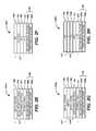
- FIGS. 1A-1Dare cross-sectional views of first exemplary metal-insulator-metal (MIM) stacks provided in accordance with the present invention.
- FIGS. 2A-2Hare cross-sectional views of second exemplary MIM stacks provided in accordance with the present invention.
- FIGS. 3A-3Dare cross-sectional views of third exemplary MIM stacks provided in accordance with the present invention.
- FIG. 4Ais a schematic illustration of an exemplary memory cell in accordance with this invention.
- FIG. 4Bis a simplified perspective view of another exemplary embodiment of a memory cell in accordance with this invention.
- FIG. 4Cis a simplified perspective view of yet another exemplary embodiment of a memory cell in accordance with this invention.
- FIG. 4Dis a simplified perspective view of a portion of a first memory level formed from a plurality of memory cells in accordance with this invention.
- FIG. 4Eis a simplified perspective view of a portion of a first monolithic three dimensional memory array that includes a first memory level positioned below a second memory level in accordance with the present invention.
- FIG. 4Fis a simplified perspective view of a portion of a second monolithic three dimensional memory array that includes a first memory level positioned below a second memory level in accordance with the present invention.
- FIGS. 5A-5Hare cross sectional views of exemplary memory cell stacks provided in accordance with the present invention.
- a metal-insulator-metal (MIM) stack formed from a reversible resistivity switching (RRS) material sandwiched between two metal or otherwise conducting layersmay serve as a resistance-switching element for a memory cell.
- the two conducting layersmay serve as the top and bottom electrodes of the resistance-switching element, and may be used to apply an electric field across the RRS material that changes the resistivity of the RRS material from a high value to a low value and vice versa.
- novel MIM stacksare provided that employ metal oxide resistivity-switching layers. Methods of forming such MIM stacks, as well as methods of employing such MIM stacks in three-dimensional (3D) memory arrays, are also provided.
- FIGS. 1A-1Dillustrate MIM stacks that employ SiGe bottom electrodes.
- FIGS. 2A-2Hillustrate MIM stacks that employ multi-layer metal-silicide bottom electrodes.
- FIGS. 3A-3Dillustrate MIM stacks that employ bottom electrodes with metal, metal nitrides or metal oxides specifically selected to promote oxygen vacancy formation in metal oxide switching layers.
- FIGS. 4A-5Hillustrate exemplary embodiments of memory cells and memory arrays that may use any of the above described MIM stacks and/or bottom electrodes.
- FIG. 1Aillustrates an MIM stack 100 a that includes a reversible resistivity switching (RRS) material 104 sandwiched between a top electrode 106 and a SiGe bottom electrode 108 .
- RTSreversible resistivity switching
- One or more additional layers 110such as a metal layer, a metal oxide layer, a metal/metal oxide layer stack, or the like, may be employed within the MIM stack 100 a as described further below.
- the RRS material 104may include, for example, HfO x , ZrO x , NiO x , TiO x , TaO x , NbO x , Al x O y , another metal oxide (MO x ) layer, any combination of these metal oxides, or another suitable switching material.
- the top electrode 106may include titanium nitride, tantalum nitride, tungsten nitride, combinations of the same, a metal/metal nitride stack such as Ti/TiN, Ta/TaN, W/WN or another similar layer.
- the top electrode 106may include heavily doped semiconductor such as n+ silicon or p+ silicon, heavily doped germanium, or heavily doped silicon-germanium. Other materials and/or configurations may be used for the top electrode 106 .
- an n+ Si bottom electrodemay improve the switching characteristics of a metal oxide such as HfO 2 by effectively lowering the free energy for forming oxygen vacancies within the metal oxide.
- a metal oxidesuch as HfO 2
- such an n+ Si electrodeis formed by depositing an amorphous or polysilicon n+ Si layer and then annealing the n+ Si layer to improve its crystallinity and surface properties prior to formation of a metal oxide layer over the n+ Si layer.
- Such an annealis generally achieved via a rapid thermal anneal (RTA) at a temperature of about 750° C.
- RTArapid thermal anneal
- use of such a high RTA temperature for each memory layermay exceed the thermal budget of the memory array.
- the bottom electrode of an MIM stackmay include a layer of SiGe alloy having, for example, between about 5 to about 35 atm % Ge and an n+ doping concentration of about 5 ⁇ 10 19 -5 ⁇ 10 21 atoms/cm 3 , in some embodiments about 2 ⁇ 10 20 atoms/cm 3 .
- a SiGe alloy layermay be formed at a substantially lower temperature than a polycrystalline n+ Si bottom electrode layer as the presence of Ge lowers the crystallization temperature.
- a polycrystalline SiGe alloy layermay be deposited at a temperature of about 600° C. or lower, and in some embodiments, about 550° C.
- an amorphous SiGe alloy layerbe deposited at a lower deposition temperature and crystallized using an RTA of about 600° C. or less, and in some embodiments, about 550° C. or less (depending on the atm % of Ge employed).
- SiGe bottom electrodes with about 5-35 atm % Gesignificantly reduce deposition and/or crystallization anneal temperatures while still providing ample Si for oxygen vacancy formation within metal oxide switching layers.
- Exemplary thicknesses for the SiGe bottom electrode 108range from about 2 to 100 nanometers.
- Other atm % of Ge, doping types, doping levels, annealing temperatures and/or layer thicknessesmay be used.
- the additional layer(s) 110may include, for example, titanium, titanium oxide, tantalum, tantalum oxide, tungsten, tungsten oxide, etc.
- the additional layer(s) 110may include a metal/metal oxide layer stack such as Ti/TiO x , Zr/ZrO x , Ni/NiO x , Al/Al x O y , Ta/TaO x , Nb/NbO x , Hf/HfO x , or any suitable layer stack.
- FIG. 1Billustrates a particular exemplary embodiment of the MIM stack 100 a of FIG. 1A , referred to as MIM stack 100 b in FIG. 1B .
- the bottom electrode 108is a SiGe alloy
- the RRS material 104is hafnium oxide
- the top electrode 106is titanium nitride
- a titanium or titanium oxide layeris provided as a buffer layer between the hafnium oxide switching material (RRS material 104 ) and the TiN top electrode 106 .
- the bottom electrode 108SiGe
- the Ti or TiO x layer 110may have a thickness of about 0.5-10 nanometers, and in some embodiments about 2 nanometers. When TiO x is employed, x may be about 1.2-2, and in some embodiments about 1.5.
- the hafnium oxide layer 104may have a thickness of about 3-12 nanometers, and in some embodiments about 5 nanometers, with x being about 1.2-2.0 and in some embodiments about 1.7.
- the TiN top electrode 106may have a thickness of about 2 to 100 nanometers, in other embodiments about 10-60 nanometers, and in some embodiments about 20 nanometers.
- the doping concentration of the n+ SiGe bottom electrode 108may be about 5 ⁇ 10 19 -5 ⁇ 10 21 atoms/cm 3 and in some embodiments about 2 ⁇ 10 20 atoms/cm 3 with about 5-35 atm % Ge. Other film thicknesses, x values, atm % of Ge and/or doping concentrations may be used.
- FIG. 1Cillustrates a cross-sectional view of another exemplary MIM stack 100 c having a SiGe bottom electrode 108 , RRS material 104 formed above the SiGe bottom electrode 108 , a metal/metal oxide layer stack 110 including metal oxide layer 110 a and metal layer 110 b formed above the RRS material 104 , and a top metal nitride electrode 106 formed above the metal/metal oxide layer stack 110 .
- the top electrode 106may include, for example, titanium nitride, tantalum nitride, tungsten nitride, combinations of the same, a metal/metal nitride stack such as Ti/TiN, Ta/TaN, W/WN or another similar barrier layer.
- the metal/metal oxide layer stack 110may include, for example, Ti/TiO x , Zr/ZrO x , Ni/NiO x , Al/Al x O y , Ta/TaO x , Nb/NbO x , Hf/HfO x or another similar layer stack.
- the RRS material 104may include, for example, HfO x , ZrO x , NiO x , TiO x , TaO x , NbO x or Al x O y , any combination of these metal oxides, or another suitable switching material.
- the metal/metal-oxide layer stack 110may be formed from a different material than is employed for the RRS material 104 .
- a Ti/TiO x layer stackmay be employed with a HfO x , ZrO x , NiO x , TaO x , NbO x or Al x O y switching material.
- a Zr/ZrO x layer stackmay be used with a HfO x , NiO x , TiO x , TaO x , NbO x or Al x O y switching material.
- a Ni/NiO x layer stackmay be used with a HfO x , ZrO x , TiO x , TaO x , NbO x or Al x O y switching material.
- An Al/Al x O y layer stackmay be employed with a HfO x , ZrO x , NiO x , TiO x , TaO x , or NbO x switching material.
- a Ta/TaO x layer stackmay be employed with a HfO x , TiO x , ZrO x , NiO x , NbO x or Al x O y switching material.
- a Nb/NbO x layer stackmay be employed with a HfO x , TiO x , ZrO x , NiO x , TaO x or Al x O y switching material.
- a Hf/HfO x layer stackmay be employed with a NbO x , TiO x , ZrO x , NiO x , TaO x or Al x O y switching material.
- the metal/metal oxide layer stack 110may be formed from a similar material to that employed for the RRS material 104 .
- a Ti/TiO x layer stackmay be employed with a TiO x switching layer.
- the metal oxide of the layer stackmay have a different crystalline structure or other property compared to that of the switching material (e.g., amorphous versus crystalline structure).
- the metal oxide layer of the metal/metal-oxide layer stack 110may serve as a “buffer” layer that allows formation/elimination of oxygen vacancies within the switching material to be more controllable and/or repeatable, which may improve the endurance/longevity of the switching material 104 .
- FIG. 1Dillustrates a particular exemplary embodiment of the MIM stack 100 c, referred to as MIM stack 100 d in FIG. 1D , in which the top electrode 106 is titanium nitride, the metal/metal oxide layer stack 110 is titanium over titanium oxide, the RRS material 104 is hafnium oxide and the bottom electrode 108 is n+ SiGe.
- the top electrode 106TiN
- TiNmay have a thickness of about 10-60 nanometers, and in some embodiments about 20 nanometers.
- the Ti layer 110 bmay have a thickness of about 0.5-10 nanometers, and in some embodiments about 2 nanometers.
- the TiO x layer 110 amay have a thickness of about 0.5-6 nanometers, and in some embodiments about 1 nanometer; and x may be about 1.2-2.0 and in some embodiments about 1.5.
- the hafnium oxide layer 104may have a thickness of about 3-12 nanometers, and in some embodiments about 5 nanometers; and x may be about 1.2-2 and in some embodiments about 1.7.
- the n+ SiGe layer 108may have a thickness of about 10-100 nanometers, and in some embodiments about 20 nanometers.
- the doping concentration of the n+ SiGe layer 106may be about 5 ⁇ 10 19 -5 ⁇ 10 21 atoms/cm 3 and in some embodiments about 2 ⁇ 10 20 atoms/cm 3 with about 5-35 atm % Ge. Other film thicknesses, x values, atm % of Ge and/or doping concentrations may be used.
- FIG. 2Aillustrates an MIM stack 200 a that includes an RRS material 104 sandwiched between a top electrode 106 and a bottom electrode 108 that includes a first metal-silicide layer 108 a and a second metal-silicide layer 108 b.
- One or more additional layers 110such as a metal layer, a metal oxide layer, a metal/metal oxide layer stack, or the like, may be employed within the MIM stack 200 a as described further below.
- the RRS material 104may include, for example, HfO x , ZrO x , NiO x , TiO x , TaO x , NbO x , Al x O y , another metal oxide (MO x ) layer, or another suitable switching material.
- the top electrode 106may include titanium nitride, tantalum nitride, tungsten nitride, combinations of the same, a metal/metal nitride stack such as Ti/TiN, Ta/TaN, W/WN or another similar layer.
- the top electrode 106may include heavily doped semiconductor such as n+ silicon or p+ silicon, heavily doped germanium, or heavily doped silicon-germanium. Other materials and/or configurations may be used for the top electrode 106 .
- n+ Si bottom electrodemay improve the switching characteristics of a metal oxide such as HfO 2 by effectively lowering the free energy for forming oxygen vacancies within the metal oxide.
- use of an n+ Si electrodetypically requires a relatively high temperature anneal (e.g., about 750° C.) to improve crystallinity and surface properties of the n+ Si electrode prior to formation of a metal oxide layer over the n+ Si layer.
- a relatively high temperature anneale.g., about 750° C.
- use of such a high temperature anneal for each memory layermay exceed the thermal budget of the memory array.
- the bottom electrode 108may include two or more layers of metal silicide.
- one or more of such metal silicide layersmay be formed at temperatures lower than 750° C., such as 600° C. or less, and in some embodiments, about 500-550° C. or less, depending on the type of silicide employed.
- cobalt silicidetypically may be formed at temperatures of about 300-800° C.
- nickel silicidetypically may be formed at temperatures of about 400-800° C., depending on factors such as the ratio of Co or Ni atoms to Si atoms.
- Titanium silicide and tungsten silicidetypically require higher formation temperatures ranging from about 500-900° C. for titanium silicide and about 1000° C. or more for tungsten silicide. In any case, use of metal silicides may still provide ample Si for oxygen vacancy formation.
- Exemplary materials that may be used for the first metal-silicide layer 108 a and/or the second metal-silicide layer 108 binclude titanium silicide, tantalum silicide, tungsten silicide, nickel silicide, cobalt silicide or molybdenum silicide, although other metal-silicides may be used.
- the lower (first) metal-silicide layer 108 amay be formed at a lower temperature than the upper (second) metal-silicide layer 108 b.
- the lower metal-silicide layer 108 amay serve as a crystallization seed layer or “template” for the upper metal-silicide layer 108 b, allowing the upper metal-silicide layer 108 b to be formed at a lower temperature.
- the first metal-silicide layer 108 amay include nickel silicide or cobalt silicide while the second metal-silicide layer 108 b may include titanium silicide.
- the first metal-silicide layer 108 amay include titanium silicide and the second metal-silicide layer 108 b may include tungsten silicide. Other combinations of silicide layers may be used.
- Exemplary thicknesses for the first and/or second metal-silicide layers 108 a and 108 brange from about 2 to about 50 nanometers. Other thicknesses may be used for either or both layers. While two metal-silicide layers are shown in FIG. 2A , it will be understood that more than two metal-silicide layers may be employed (e.g., 3, 4, 5, etc.).
- the additional layer(s) 110may include, for example, titanium, titanium oxide, tantalum, tantalum oxide, tungsten, tungsten oxide, etc.
- the additional layer(s) 110may include a metal/metal oxide layer stack such as Ti/TiO x , Zr/ZrO x , Ni/NiO x , Al/Al x O y , Ta/TaO x , Nb/NbO x , Hf/HfO x , or any suitable layer stack.
- FIG. 2Billustrates a particular exemplary embodiment of the MIM stack 200 a of FIG. 2A , referred to as MIM stack 200 b in FIG. 2B .
- the bottom electrode 108is a multi-layer metal-silicide stack
- the RRS material 104is hafnium oxide
- the top electrode 106is titanium nitride
- a titanium or titanium oxide layeris provided as a buffer layer between the hafnium oxide switching material (RRS material 104 ) and the TiN top electrode 106 .
- each metal-silicide layer 108 a or 108 b of the bottom electrode 108may have a thickness of about 2 to 50 nanometers, in other embodiments about 5-25 nanometers, and in some embodiments about 20 nanometers.
- the Ti or TiO x layer 110may have a thickness of about 0.5-10 nanometers, and in some embodiments about 2 nanometers. When TiO x is employed, x may be about 1.2-2, and in some embodiments about 1.5.
- the hafnium oxide layer 104may have a thickness of about 3-12 nanometers, and in some embodiments about 5 nanometers, with x being about 1.2-2.0 and in some embodiments about 1.7.
- the TiN top electrode 106may have a thickness of about 2 to 100 nanometers, in other embodiments about 10-60 nanometers, and in some embodiments about 20 nanometers. Other film thicknesses, x values and/or doping concentrations may be used.
- FIG. 2Cillustrates a cross-sectional view of another exemplary MIM stack 200 c having a multi-layer silicide bottom electrode 108 , RRS material 104 formed above the bottom electrode 108 , a metal/metal oxide layer stack 110 including metal oxide layer 110 a and metal layer 110 b formed above the RRS material 104 , and a top metal nitride electrode 106 formed above the metal/metal oxide layer stack 110 .
- the top electrode 106may include, for example, titanium nitride, tantalum nitride, tungsten nitride, combinations of the same, a metal/metal nitride stack such as Ti/TiN, Ta/TaN, W/WN or another similar barrier layer.
- the metal/metal oxide layer stack 110may include, for example, Ti/TiO x , Zr/ZrO x , Ni/NiO x , Al/Al x O y , Ta/TaO x , Nb/NbO x , Hf/HfO x or another similar layer stack.
- the RRS material 104may include, for example, HfO x , ZrO x , NiO x , TiO x , TaO x , NbO x or Al x O y or another suitable switching material.
- the metal/metal-oxide layer stack 110may be formed from a different material than is employed for the RRS material 104 .
- a Ti/TiO x layer stackmay be employed with a HfO x , ZrO x , NiO x , TaO x , NbO x or Al x O y switching material.
- a Zr/ZrO x layer stackmay be used with a HfO x , NiO x , TiO x , TaO x , NbO x or Al x O y switching material.
- a Ni/NiO x layer stackmay be used with a HfO x , ZrO x , TiO x , TaO x , NbO x or Al x O y switching material.
- An Al/Al x O y layer stackmay be employed with a HfO x , ZrO x , NiO x , TiO x , TaO x , or NbO x switching material.
- a Ta/TaO x layer stackmay be employed with a HfO x , TiO x , ZrO x , NiO x , NbO x or Al x O y switching material.
- a Nb/NbO x layer stackmay be employed with a HfO x , TiO x , ZrO x , NiO x , TaO x or Al x O y switching material.
- a Hf/HfO x layer stackmay be employed with a NbO x , TiO x , ZrO x , NiO x , TaO x or Al x O y switching material.
- the metal/metal oxide layer stack 110may be formed from a similar material to that employed for the RRS material 104 .
- a Ti/TiO x layer stackmay be employed with a TiO x switching layer.
- the metal oxide of the layer stackmay have a different crystalline structure or other property compared to that of the switching material (e.g., amorphous versus crystalline structure).
- FIG. 2Dillustrates a particular exemplary embodiment of the MIM stack 200 c, referred to as MIM stack 200 d in FIG. 2D , in which the top electrode 106 is titanium nitride, the metal/metal oxide layer stack 110 is titanium over titanium oxide, the RRS material 104 is hafnium oxide and the bottom electrode 108 is a multi-layer metal-silicide stack.
- the top electrode 106TiN
- TiNmay have a thickness of about 10-60 nanometers, and in some embodiments about 20 nanometers.
- the Ti layer 110 bmay have a thickness of about 0.5-10 nanometers, and in some embodiments about 2 nanometers.
- the TiO x layer 110 amay have a thickness of about 0.5-6 nanometers, and in some embodiments about 1 nanometer; and x may be about 1.2-2.0 and in some embodiments about 1.5.
- the hafnium oxide layer 104may have a thickness of about 3-12 nanometers, and in some embodiments about 5 nanometers; and x may be about 1.2-2 and in some embodiments about 1.7.
- Each metal-silicide layer 108 a or 108 bmay have a thickness of about 2-50 nanometers, and in some embodiments about 25 nanometers. Other film thicknesses, x values and/or doping concentrations may be used.
- FIG. 2Eillustrates an alternative exemplary embodiment of the MIM stack 200 a of FIG. 2A , referred to as MIM stack 200 e in FIG. 2E .
- the MIM stack 200 e of FIG. 2Eis similar to the MIM stack 200 a of FIG. 2A , but includes an additional metal (M), metal nitride (MN x ) or metal oxide (MO x ) layer 212 positioned between the RRS material 104 and the multi-layer metal-silicide layer stack 108 (and that may form part of the bottom electrode 108 ).
- Madditional metal
- MN xmetal nitride
- MO xmetal oxide
- the metal, metal nitride or metal oxide layer 212may include one or more of silicon, silicon nitride or oxide, aluminum, aluminum nitride or oxide, lanthanum, lanthanum nitride or oxide, molybdenum, molybdenum nitride or oxide, tantalum, tantalum nitride or oxide, chromium, chromium nitride or oxide, hafnium, hafnium nitride or oxide, niobium, niobium nitride or oxide, vanadium, vanadium nitride or oxide, zirconium, or zirconium nitride or oxide.
- an alloysuch as n+ SiGe may be used as the metal, metal nitride or metal oxide layer 212 .
- Other materialsmay also be employed.
- Certain metalsmay promote oxygen vacancy formation in metal oxides by making oxygen vacancy formation more energetically favorable, effectively reducing the Gibbs free energy of forming oxygen vacancies within the metal oxides. See, for example, Roberston et al., “Fermi level pinning by defects in HfO 2 -metal gate stacks,” Appl. Phys. Letters 91, 132912 (2007), which describes oxygen vacancy formation in a HfO 2 gate oxide/Si channel system.
- the additional metal, metal nitride or metal oxide layer 212may be selected so as to have a Gibbs free energy of formation per O between about ⁇ 3 and ⁇ 6 eV so as to promote oxygen vacancy formation within the metal oxide RRS material 104 .
- Exemplary metals that may be suitableinclude, for example, Yb, Tb, Y, So, La, Hf, Mg, Zr, Ta, Nb, V, Zn, W, Mo, Ti, Al, Cr, Si, Ni, Re, Co, Cu, Ru, Rh, Pd, and Ir.
- Metal nitrides (or metal oxides) of these metalsmay render oxygen vacancy formation energetically more favorable within resistivity-switching metal oxides.
- the additional metal, metal nitride or metal oxide layer 212may be formed from one or more metals, metal nitrides or metal oxides of the above-listed materials, or any other materials having a Gibbs free energy of formation per O between about ⁇ 3 and ⁇ 6 eV.
- Exemplary thicknesses for the metal, metal nitride or metal oxide layer 212may range from about 10 to about 100 angstroms. Other thicknesses may be used.
- FIGS. 2F-2Hillustrate MIM stacks 200 f - 200 h that are similar to the MIM stacks 200 b - 200 d of FIGS. 2B-2D , but include the metal, metal nitride or metal oxide layer 212 .
- FIGS. 3A-3Dillustrates alternative embodiments of the MIM stacks 200 e - 200 h of FIGS. 2E-2H , referred to as MIM stacks 300 a - d in FIGS. 3A-3D , in which a metal, metal nitride or metal oxide layer such as the metal, metal nitride or metal oxide layer 212 is used as the bottom electrode 108 without the first and second metal-silicide layers 108 a and 108 b.
- a metal, metal nitride or metal oxide layersuch as the metal, metal nitride or metal oxide layer 212 is used as the bottom electrode 108 without the first and second metal-silicide layers 108 a and 108 b.
- the metal, metal nitride or metal oxide bottom electrode 108may include one or more of silicon, silicon nitride or oxide, aluminum, aluminum nitride or oxide, lanthanum, lanthanum nitride or oxide, molybdenum, molybdenum nitride or oxide, tantalum, tantalum nitride or oxide, chromium, chromium nitride or oxide, hafnium, hafnium nitride or oxide, niobium, niobium nitride or oxide, vanadium, vanadium nitride or oxide, zirconium or zirconium nitride or oxide. Other materials may also be employed.
- the metal, metal nitride or metal oxide bottom electrode 108may be selected to promote oxygen vacancy formation in the metal oxide switching layer 104 .
- the metal, metal nitride or metal oxide bottom electrode 108may be selected so as to have a Gibbs free energy of formation per O between about ⁇ 3 and ⁇ 6 eV.
- Exemplary metals that may fall within this rangeinclude, for example, Yb, Tb, Y, So, La, Hf, Mg, Zr, Ta, Nb, V, Zn, W, Mo, Ti, Al, Cr, Si, Ni, Re, Co, Cu, Ru, Rh, Pd, and Ir.
- Metal nitrides (or metal oxides) of these metalsmay similarly render oxygen vacancy formation more energetically favorable within resistivity-switching metal oxides. Accordingly, in some embodiments, the metal, metal nitride or metal oxide bottom electrode 108 may be formed from one or more metals, metal nitrides or metal oxides of the above-listed materials, or any other materials having a Gibbs free energy of formation per O between about ⁇ 3 and ⁇ 6 eV.
- Exemplary thicknesses for the metal, metal nitride or metal oxide bottom electrode 108may range from about 10 to about 100 angstroms. Other thicknesses may be used.
- the metal, metal nitride or metal oxide bottom electrode 108may include chromium, chromium nitride, hafnium, hafnium nitride, niobium, niobium nitride, vanadium, vanadium nitride, zirconium or zirconium nitride.
- FIG. 4Ais a schematic illustration of an exemplary memory cell 400 in accordance with this invention.
- Memory cell 400includes MIM stack 402 coupled to a steering element 404 .
- MIM stack 402includes RRS material 104 (not separately shown) which has a resistivity that may be reversibly switched between two or more states, and may be similar to any of the MIM stacks described previously with reference to FIGS. 1A-3D .
- Steering element 404may include a thin film transistor, a diode, a metal-insulator-metal tunneling current device, a punch-through diode, a Schottky-diode or another similar steering element that exhibits non-ohmic conduction by selectively limiting the voltage across and/or the current flow through MIM stack 402 .
- memory cell 400may be used as part of a two or three dimensional memory array and data may be written to and/or read from memory cell 400 without affecting the state of other memory cells in the array.
- steering element 404may be omitted, and memory cell 400 may be used with a remotely located steering element.
- FIG. 4Bis a simplified perspective view of an exemplary embodiment of memory cell 400 in accordance with this invention in which steering element 404 is a diode.
- Memory cell 400includes MIM stack 402 (having RRS material 104 ) coupled in series with diode 404 between a first conductor 406 a and a second conductor 406 b.
- MIM stack 402may serve as a reversible resistance-switching element for the memory cell 400 .
- the MIM stack 402may be similar to any of MIM stacks of FIGS. 1A-3D , or any other suitable MIM stack, and may include a top conducting layer 106 and a bottom conducting layer 108 that surround RRS material 104 and serve as top and bottom electrodes for the MIM stack 402 .
- One or more additional layers 110such as a metal layer, a metal oxide layer, a metal/metal oxide layer stack, or the like, may be employed within the MIM stack 402 as described previously.
- a barrier layer 408may be formed between MIM stack 402 and diode 404
- a barrier layer 410may be formed between MIM stack 402 and second conductor 406 b
- An additional barrier layer 412may be formed between diode 404 and first conductor 406 a.
- Barrier layers 408 , 410 and 412may include titanium, titanium nitride, tantalum, tantalum nitride, tungsten, tungsten nitride, molybdenum, combinations of the same, or another similar barrier layer.
- Barrier layer 210may be separate from or part of second conductor 406 b and barrier layer 412 may be separate from or part of first conductor 406 a.
- Diode 404may include any suitable diode such as a vertical polycrystalline p-n or p-i-n diode, whether upward pointing with an n-region above a p-region of the diode or downward pointing with a p-region above an n-region of the diode, a p-n-p or n-p-n punch through diode, a Schottky diode or the like. Exemplary embodiments of diode 204 are described below with reference to FIGS. 5A-5H .
- the MIM stack 402is positioned above diode 404 .
- the MIM stack 402alternatively may be positioned below the diode 404 .
- First conductor 406 a and/or second conductor 406 bmay include any suitable conductive material such as tungsten, any appropriate metal, heavily doped semiconductor material, a conductive silicide, a conductive silicide-germanide, a conductive germanide, a highly conductive carbon or the like.
- first and second conductors 406 a and 406 bare line or rail-shaped and extend in different directions (e.g., substantially perpendicular to one another). Other conductor shapes and/or configurations may be used.
- barrier layers, adhesion layers, antireflection coatings and/or the likemay be used with first conductor 406 a and/or second conductor 406 b to improve device performance and/or aid in device fabrication.
- FIG. 4Dis a simplified perspective view of a portion of a first memory level 414 formed from a plurality of memory cells 400 , such as memory cells 400 of FIG. 4A or 4 B.
- RRS material 104conductive layers 106 and 108 , additional layer(s) 110 , diode 404 , and barrier layers 408 , 410 and 412 are not separately shown.
- Memory array 414is a “cross-point” array including a plurality of bit lines (second conductors 406 b ) and word lines (first conductors 406 a ) to which multiple memory cells are coupled (as shown). Other memory array configurations may be used, as may multiple levels of memory.
- FIG. 4Eis a simplified perspective view of a portion of a monolithic three dimensional memory array 416 a that includes a first memory level 418 positioned below a second memory level 420 .
- Memory levels 418 and 420each include a plurality of memory cells 400 in a cross-point array.
- additional layerse.g., an interlevel dielectric
- FIG. 4EOther memory array configurations may be used, as may additional levels of memory.
- all diodesmay “point” in the same direction (have the same “steering element” polarity orientation), such as upward or downward depending on whether p-i-n diodes having a p-doped region on the bottom or top of the diodes are employed, simplifying diode fabrication.
- the memory levelsmay be formed as described in U.S. Pat. No. 6,952,030, titled “High-Density Three-Dimensional Memory Cell,” which is hereby incorporated by reference herein in its entirety for all purposes.
- the second (top) conductors of a first memory levelmay be used as the first (bottom) conductors of a second memory level that is positioned above the first memory level as shown in FIG. 4F .
- the diodes on adjacent memory levelspreferably point in opposite directions as described in U.S. patent application Ser. No. 11/692,151, filed Mar.
- the diodes of first memory level 418may be upward pointing diodes as indicated by arrow D 1 (e.g., with p regions at the bottom of the diodes), whereas the diodes of second memory level 420 may be downward pointing diodes as indicated by arrow D 2 (e.g., with n regions at the bottom of the diodes), or vice versa.
- MIM stacks 402are bipolar, in embodiments in which conductors are shared between memory levels as in FIG. 4F , MIM stacks 402 may be arranged to have the same voltage polarity orientation within a memory level, but opposite voltage polarity orientations between adjacent memory levels. For example, the MIM stacks 402 of first memory level 418 may be positively oriented whereas the MIM stacks 402 of the second memory level 420 may be negatively oriented, or vice versa.
- the diodes 404may be oriented to be reversed biased during the set operations of the MIM stacks 402 . Alternatively, the diodes 404 may be oriented to be forward biased during the set operations of the MIM stacks 402 .
- a monolithic three dimensional memory arrayis one in which multiple memory levels are formed above a single substrate, such as a wafer, with no intervening substrates.
- the layers forming one memory levelare deposited or grown directly over the layers of an existing level or levels.
- stacked memorieshave been constructed by forming memory levels on separate substrates and adhering the memory levels atop each other, as in Leedy, U.S. Pat. No. 5,915,167, titled “Three Dimensional Structure Memory.”
- the substratesmay be thinned or removed from the memory levels before bonding, but as the memory levels are initially formed over separate substrates, such memories are not true monolithic three dimensional memory arrays.
- FIG. 5Ais a cross sectional view of a first memory cell 500 a provided in accordance with the present invention. Additional memory cells (not shown) may be provided at each memory level as described in FIGS. 4D-F .
- memory cell 500 aincludes a MIM stack 502 a coupled in series with a diode 504 a between bit line 506 a and word line 506 b.
- MIM stack 502 ahas a positive polarity orientation such that a positive voltage applied to word line 506 b relative to bit line 506 a may be employed to set the MIM stack 502 a.
- Diode 504 ais oriented so as to be reversed biased during such a set operation. In other embodiments, diode 504 a may be oriented so as to be forward biased while a set operation is performed on the MIM stack 502 a.
- MIM stack 502 amay include any of the MIM stacks previously described, or any other suitable MIM stack. In FIG. 5A , MIM stack 502 a is shown as being similar to MIM stack 100 d ( FIG. 1D ).
- Diode 504 amay include any two terminal, non-linear steering element such as a p-n or p-i-n junction diode, a punch through diode, a tunneling oxide device, a Schottky diode, or the like. In FIG. 5A , diode 504 a is shown as being a p-i-n junction diode.
- bit line 506 aincludes bit line 506 a.
- Bit line 506 amay be about 200 to about 2500 angstroms of any suitable conductive material such as tungsten or another appropriate metal, heavily doped semiconductor material, a conductive silicide, a conductive silicide-germanide, a conductive germanide, or the like.
- a plurality of bit lines 506 amay be formed as substantially parallel, substantially co-planar bit lines 506 a.
- Exemplary widths for bit lines 506 a and/or spacings between bit lines 506 arange from about 200 to about 2500 angstroms, although other conductor widths and/or spacings may be used.
- Bit lines 506 amay be separated from one another by dielectric material (not shown) such as silicon dioxide, silicon nitride, silicon oxynitride, low K dielectric, etc., and/or other dielectric materials.
- Barrier layer 512is formed over bit line 506 a.
- Barrier layer 512may be about 20 to about 500 angstroms, and in some embodiments about 100 angstroms, of titanium nitride or another suitable barrier layer such as tantalum nitride, tungsten nitride, tungsten, molybdenum, combinations of one or more barrier layers, barrier layers in combination with other layers such as titanium/titanium nitride, tantalum/tantalum nitride or tungsten/tungsten nitride stacks, or the like. Other barrier layer materials and/or thicknesses may be employed.
- the diode 504 ais formed from a polycrystalline semiconductor material such as polysilicon, a polycrystalline silicon-germanium alloy, polygermanium or any other suitable material.
- a heavily doped amorphous or polycrystalline p+ silicon layer 504 a - 1may be deposited on barrier layer 512 .
- CVD or another suitable processmay be employed to deposit p+ silicon layer 504 a - 1 .
- p+ silicon layer 504 a - 1may be formed, for example, from about 100 to about 1000 angstroms, in some embodiments about 100 angstroms, of p+ silicon with a doping concentration of about 10 21 cm ⁇ 3 . Other layer thicknesses and/or doping concentrations may be used. P+ silicon layer 504 a - 1 may be doped in situ, for example, by flowing an acceptor gas during deposition, or ex situ, for example, via implantation.
- a lightly doped, intrinsic and/or unintentionally doped amorphous or polycrystalline silicon layer 504 a - 2may be formed over p+ silicon layer 504 a - 1 .
- CVD or another suitable deposition methodmay be employed to deposit intrinsic silicon layer 504 a - 2 .
- intrinsic silicon layer 504 a - 2may be about 500 to about 4800 angstroms, in some embodiments about 2500 angstroms, in thickness. Other intrinsic layer thicknesses may be used.
- n+ silicon layer 504 a - 3may be deposited and doped by ion implantation or doped in situ during deposition to form an n+ silicon layer 504 a - 3 . Further, in some embodiments, a diffusion process may be employed. In at least one embodiment, the resultant n+ silicon layer 504 a - 3 may have a thickness of about 100 to about 1000 angstroms, in some embodiments about 100 angstroms, with a doping concentration of about 10 21 cm ⁇ 3 . Other layer thicknesses and/or doping concentrations may be used.
- a silicide-forming metal layer stack 508may be deposited over n+ silicon layer 504 a - 3 .
- exemplary silicide-forming metalsinclude sputter or otherwise deposited titanium or cobalt.
- a silicide-forming metal layer stack 508is formed from about 1-4 nanometers of titanium and about 15-25 nanometers of titanium nitride. Other silicide-forming metal layer materials and/or thicknesses may be used.
- a rapid thermal anneal (“RTA”) stepmay be performed to form a silicide region by reaction of silicide-forming metal such as Ti with n+ region 504 a - 3 .
- the RTAmay be performed at about 540° C. for about 1 minute, to cause silicide-forming metal and the deposited silicon of diode 504 a to interact to form a silicide layer, consuming all or a portion of the silicide-forming metal.
- a silicide layermay be formed by sputtering a silicide target or by co-sputtering silicide forming metal and silicon.
- silicide-forming materialssuch as titanium and/or cobalt react with deposited silicon during annealing to form a silicide layer.
- silicide layersmay serve as “crystallization templates” or “seeds” for adjacent deposited silicon as the deposited silicon crystallizes (e.g., a silicide layer may enhance the crystalline structure of silicon diode 504 a during annealing). Lower resistivity silicon thereby is provided. Similar results may be achieved for silicon-germanium alloy and/or germanium diodes.
- bottom electrode 108 of MIM stack 502 amay be formed.
- bottom electrode 108may include a layer of SiGe alloy having, for example, between about 5 to about 35 atm % Ge and an n+ doping concentration of about 5 ⁇ 10 19 -5 ⁇ 10 21 atoms/cm 3 , and in some embodiments about 2 ⁇ 10 20 atoms/cm 3 .
- SiGe bottom electrodes with about 5-35 atm % Gesignificantly reduce crystalline anneal temperatures while still providing ample Si for oxygen vacancy formation.
- low temperature processessuch as low pressure chemical vapor deposition (LPCVD) or plasma enhanced chemical vapor deposition (PECVD) may be employed to form the SiGe bottom electrode 108 .
- Exemplary temperature ranges at which the SiGe bottom electrode 108 may be formed (crystallized)are 600° C. or less, and in some embodiments 550° C. or less.
- Exemplary thicknesses for the SiGe bottom electrode 108range from about 2 to 100 nanometers. Other atm % of Ge, doping types, doping levels, formation temperatures and/or layer thicknesses may be used in other embodiments.
- RRS material 104may be formed by atomic layer deposition (ALD) or another suitable method.
- the RRS material 104may include HfO x , ZrO x , NiO x , TiO x , TaO x , NbO x , Al x O y , combinations of one or more of these metal oxides, or another suitable switching material.
- the RRS material 104may include HfO x having a thickness of about 3-12 nanometers, and in some embodiments about 5 nanometers, with x being about 1.2-2.0 and in some embodiments about 1.7. Other thickness ranges and/or x values may be used.
- a metal/metal oxide layer stack 110may be formed.
- the metal/metal oxide layer stack 110may include, for example, Ti/TiO x , Zr/ZrO x , Ni/NiO x , Al/Al x O y , Ta/TaO x , Nb/NbO x , Hf/HfO x or another similar layer stack.
- the metal/metal oxide layer stack 110may include Ti layer 110 b having a thickness of about 0.5-10 nanometers, and in some embodiments about 2 nanometers and TiO x layer 110 a having a thickness of about 0.5-6 nanometers, and in some embodiments about 1 nanometer; and x may be about 1.2-2.0 and in some embodiments about 1.5. Other thicknesses and/or x values may be used.
- the TiO x layer 110 amay be formed, for example, by depositing a layer of Ti over the HfO x layer 104 and then oxidizing the Ti to form the TiO x layer 110 a.
- a layer of Timay be deposited via PVD and then oxidized in the same ALD chamber used to form the HfO x layer 104 (e.g., by not flowing the Hf precursor).
- the Ti layer 110 bmay then be formed over the TiO x layer 110 a.
- Top electrode 106is formed over Ti layer 110 b.
- top electrode 106may include titanium nitride, tantalum nitride, tungsten nitride, combinations of the same, a metal/metal nitride stack such as Ti/TiN, Ta/TaN, W/WN or another similar barrier layer.
- the top electrode 106may include about 10-60 nanometers, and in some embodiments about 20 nanometers of TiN. Other layer thicknesses may be used.
- n+ SiGe layer 108 , HfO x layer 104 , TiO x layer 110 a, Ti Layer 110 b and/or TiN layer 106may be formed in a single cluster tool (e.g., without breaking vacuum) to improve the interfaces between the various layers.
- any suitable etch processmay be used.
- a hard mask processmay be employed as follows:
- the TiN top electrode 106may be etched using, for example, HBr, Cl 2 , and/or He; the Ti/TiO x metal layer stack 110 may be etched using, for example, CF 4 , Cl 2 , He, and/or N 2; the HfO x RRS material 104 may be etched using, for example, HBr, Cl 2 , He, and/or N 2 ; the n+ SiGe bottom electrode 108 may be etched using, for example, HBr, Cl 2 , He, O 2 and/or N 2 ; the Ti/TiN layer stack 508 may be etched using, for example, HBr, Cl 2 , and/or He; the polysilicon diode 504 a may be etched using, for example, HBr, Cl 2 , He, O 2 and/or N 2 ; and the TiN layer 512 may be etched using, for example, HBr, Cl 2 , and/or He. All of these etch processes may be performed
- the resulting pillar structure 514may be surrounded by a suitable dielectric to isolate it from other similar pillar structures (not shown) on the same memory level.
- a suitable dielectricFor example, approximately 200-7000 angstroms of silicon dioxide may be deposited and planarized using chemical mechanical polishing or an etchback process to remove excess dielectric material and form a planar surface for receiving word line 506 b.
- a thin silicon nitride linersuch as about 50 to 200 angstroms, may be deposited prior to silicon dioxide deposition.
- Word line 506 bmay be formed from any suitable conductive material such as tungsten, another suitable metal, heavily doped semiconductor material, a conductive silicide, a conductive silicide-germanide, a conductive germanide, or the like deposited by any suitable method (e.g., CVD, PVD, etc.). Other conductive layer materials may be used. For example, conductive material may be deposited and etched to form word line 506 b (and other word lines not separately shown). In at least one embodiment, such word lines are substantially parallel, substantially coplanar conductors that extend in a different direction than bit line(s) 506 a (as shown in FIG. 4F , for example).
- Word line 506 bmay be isolated from other word lines via a suitable dielectric fill and etchback process. Thereafter, an additional memory cell (not shown) may be formed over the word line 506 b in a manner similar to that used to form the memory cell 500 a.
- the resultant structuremay be annealed to crystallize the deposited semiconductor material of diode 504 a (and/or to form silicide regions by reaction of silicide-forming metal from layer 508 with silicon region(s) of the diode 504 a ).
- silicide layersmay serve as “crystallization templates” or “seeds” for adjacent deposited silicon as the deposited silicon crystallizes (e.g., a silicide layer may enhance the crystalline structure of silicon diodes during annealing at temperatures of about 600-800° C.). Lower resistivity diode material thereby is provided. Similar results may be achieved for silicon-germanium alloy and/or germanium diodes.
- a crystallization annealmay be performed for about 10 seconds to about 2 minutes in nitrogen at a temperature of about 600 to 800° C., and in some embodiments between about 650 and 750° C. Other annealing times, temperatures and/or environments may be used.
- FIG. 5Bis a cross sectional view of a second memory cell 500 b provided in accordance with the present invention.
- the second memory cell 500 b of FIG. 5Bis similar to the first memory cell 500 a of FIG. 5A , but employs a unipolar steering element in place of the bipolar steering element employed by the first memory cell 500 a.
- the diode 504 b in FIG. 5Bis a punch through diode rather than a p-i-n junction diode as is used in the memory cell 500 a of FIG. 5A .
- other steering elementsmay be used such as tunneling devices, Schottky diodes or the like.
- FIG. 5Cis a cross sectional view of a third memory cell 500 c provided in accordance with the present invention.
- the third memory cell 500 c of FIG. 5Cis similar to the first memory cell 500 a of FIG. 5A (and may be similarly formed), but employs a bi-layer metal-silicide bottom electrode 108 (as described previously with reference to FIGS. 2A-2D ).
- FIG. 5Dis a cross sectional view of a fourth memory cell 500 d provided in accordance with the present invention.
- the fourth memory cell 500 d of FIG. 5Dis similar to the third memory cell 500 c of FIG. 5C , but employs a unipolar steering element in place of the bipolar steering element employed by the third memory cell 500 c.
- the diode 504 d in FIG. 5Dis a punch through diode rather than a p-i-n junction diode as is used in the memory cell 500 c of FIG. 5C .
- other steering elementsmay be used such as tunneling devices, Schottky diodes or the like.
- FIG. 5Eis a cross sectional view of a fifth memory cell 500 e provided in accordance with the present invention.
- the fifth memory cell 500 e of FIG. 5Eis similar to the first memory cell 500 a of FIG. 5A (and may be similarly formed), but employs a metal-silicide bi-layer with an additional metal, metal nitride or metal oxide layer 112 for the bottom electrode (as described previously with reference to FIGS. 2E-2H ).
- FIG. 5Fis a cross sectional view of a sixth memory cell 500 f provided in accordance with the present invention.
- the sixth memory cell 500 f of FIG. 5Fis similar to the fifth memory cell 500 e of FIG. 5E , but employs a unipolar steering element in place of the bipolar steering element employed by the fifth memory cell 500 e.
- the diode 504 f in FIG. 5Fis a punch through diode rather than a p-i-n junction diode as is used in the memory cell 500 e of FIG. 5E .
- other steering elementsmay be used such as tunneling devices, Schottky diodes or the like.
- FIG. 5Gis a cross sectional view of a seventh memory cell 500 g provided in accordance with the present invention.
- the seventh memory cell 500 g of FIG. 5Gis similar to the first memory cell 500 a of FIG. 5A (and may be similarly formed), but employs a metal, metal nitride or metal oxide layer for the bottom electrode 108 (as described previously with reference to FIGS. 3A-3D ).
- FIG. 5His a cross sectional view of an eighth memory cell 500 h provided in accordance with the present invention.
- the eighth memory cell 500 h of FIG. 5His similar to the seventh memory cell 500 g of FIG. 5G , but employs a unipolar steering element in place of the bipolar steering element employed by the seventh memory cell 500 g.
- the diode 504 h in FIG. 5His a punch through diode rather than a p-i-n junction diode as is used in the memory cell 500 g of FIG. 5G .
- other steering elementsmay be used such as tunneling devices, Schottky diodes or the like.
- MIM stacksmay be placed above or below steering elements within any memory cells.
Landscapes
- Engineering & Computer Science (AREA)
- Manufacturing & Machinery (AREA)
- Semiconductor Memories (AREA)
Abstract
Description
- The present application claims priority to U.S. Provisional Patent Application Ser. No. 61/314,577, filed Mar. 16, 2010 and titled “ELECTRODES FOR USE WITH RESISTIVITY SWITCHING MATERIALS”, which is hereby incorporated by reference herein in its entirety for all purposes.
- The present invention relates to memory arrays and more particularly to bottom electrodes for use with metal oxide resistivity switching layers.
- Reversible resistivity-switching (RRS) materials such as metal oxides may be used as storage elements in memory arrays. For example, U.S. Pat. No. 7,812,404, filed May 9, 2005 and titled “NON-VOLATILE MEMORY CELL COMPRISING A DIODE AND A RESISTANCE-SWITCHING MATERIAL”, which is hereby incorporated by reference herein in its entirety, describes a rewriteable non-volatile memory cell that includes a diode coupled in series with an RRS material such as a metal oxide or metal nitride.
- However, fabricating memory devices from metal oxide rewriteable resistivity-switching materials with desirable switching characteristics is difficult; and improved memory devices that employ metal oxide resistivity-switching materials are desirable.
- In a first aspect of the invention, a metal-insulator-metal (MIM) stack is provided that includes (1) a first conductive layer comprising a silicon-germanium (SiGe) alloy; (2) a resistivity-switching layer comprising a metal oxide layer formed above the first conductive layer; and (3) a second conductive layer formed above the resistivity-switching layer. A memory cell may be formed from the MIM stack.
- In a second aspect of the invention, a method of forming an MIM stack is provided that includes (1) forming a first conductive layer comprising a SiGe alloy; (2) forming a resistivity-switching layer comprising a metal oxide layer above the first conductive layer; and (3) forming a second conductive layer above the resistivity-switching layer.
- In a third aspect of the invention, a method of forming a memory cell is provided that includes (1) forming an MIM stack having (a) a first conductive layer comprising a SiGe alloy; (b) a resistivity-switching layer comprising a metal oxide layer formed above the first conductive layer; and (c) a second conductive layer formed above the resistivity-switching layer; and (2) forming a steering element coupled to the MIM stack.
- In a fourth aspect of the invention, an MIM stack is provided that includes (1) a first conductive layer comprising a first metal-silicide layer and a second metal-silicide layer; (2) a resistivity-switching layer comprising a metal oxide layer formed above the first conductive layer; and (3) a second conductive layer formed above the resistivity-switching layer. A memory cell may be formed from the MIM stack.
- In a fifth aspect of the invention, a method of forming an MIM stack includes (1) forming a first conductive layer comprising a first metal-silicide layer and a second metal-silicide layer; (2) forming a resistivity-switching layer comprising a metal oxide layer above the first conductive layer; and (3) forming a second conductive layer above the resistivity-switching layer. A memory cell may be formed using the method.
- In a sixth aspect of the invention, an MIM is provided that includes (1) a first metal-silicide layer formed at a first temperature; (2) a second metal-silicide layer formed above the first metal-silicide layer and at a second temperature that is greater than the first temperature; (3) an n+ silicon or SiGe layer formed above the second metal-silicide layer; (4) a resistivity-switching layer comprising a metal oxide layer formed above the n+ silicon or SiGe layer; and (5) a second conductive layer formed above the resistivity-switching layer. A memory cell may be formed from the MIM stack.
- In a seventh aspect of the invention, a method of forming an MIM stack includes (1) forming a first metal-silicide layer at a first temperature; (2) forming a second metal-silicide layer above the first metal-silicide layer at a second temperature that is greater than the first temperature; (3) forming an n+ silicon or SiGe layer above the second metal-silicide layer; (4) forming a resistivity-switching layer comprising a metal oxide layer above the n+ silicon or SiGe layer; and (5) forming a second conductive layer above the resistivity-switching layer. A memory cell may be formed using the method.
- In an eighth aspect of the invention, an MIM stack is provided that includes (1) a first conductive layer comprising one or more of chromium, chromium nitride, hafnium, hafnium nitride, niobium, niobium nitride, vanadium, vanadium nitride, zirconium or zirconium nitride; (2) a resistivity-switching layer comprising a metal oxide layer formed above the first conductive layer; and (3) a second conductive layer formed above the resistivity-switching layer. A memory cell may be formed from the MIM stack.
- In a ninth aspect of the invention, a method of forming an MIM stack is provided that includes (1) forming a first conductive layer comprising one or more of chromium, chromium nitride, hafnium, hafnium nitride, niobium, niobium nitride, vanadium, vanadium nitride, zirconium or zirconium nitride; (2) forming a resistivity-switching layer comprising a metal oxide layer above the first conductive layer; and (3) forming a second conductive layer above the resistivity-switching layer. A memory cell may be formed using the method. Numerous other aspects are provided.
- Other features and aspects of this invention will become more fully apparent from the following detailed description, the appended claims and the accompanying drawings.
FIGS. 1A-1D are cross-sectional views of first exemplary metal-insulator-metal (MIM) stacks provided in accordance with the present invention.FIGS. 2A-2H are cross-sectional views of second exemplary MIM stacks provided in accordance with the present invention.FIGS. 3A-3D are cross-sectional views of third exemplary MIM stacks provided in accordance with the present invention.FIG. 4A is a schematic illustration of an exemplary memory cell in accordance with this invention.FIG. 4B is a simplified perspective view of another exemplary embodiment of a memory cell in accordance with this invention.FIG. 4C is a simplified perspective view of yet another exemplary embodiment of a memory cell in accordance with this invention.FIG. 4D is a simplified perspective view of a portion of a first memory level formed from a plurality of memory cells in accordance with this invention.FIG. 4E is a simplified perspective view of a portion of a first monolithic three dimensional memory array that includes a first memory level positioned below a second memory level in accordance with the present invention.FIG. 4F is a simplified perspective view of a portion of a second monolithic three dimensional memory array that includes a first memory level positioned below a second memory level in accordance with the present invention.FIGS. 5A-5H are cross sectional views of exemplary memory cell stacks provided in accordance with the present invention.- A metal-insulator-metal (MIM) stack formed from a reversible resistivity switching (RRS) material sandwiched between two metal or otherwise conducting layers may serve as a resistance-switching element for a memory cell. The two conducting layers may serve as the top and bottom electrodes of the resistance-switching element, and may be used to apply an electric field across the RRS material that changes the resistivity of the RRS material from a high value to a low value and vice versa.
- In accordance with embodiments of the present invention, novel MIM stacks are provided that employ metal oxide resistivity-switching layers. Methods of forming such MIM stacks, as well as methods of employing such MIM stacks in three-dimensional (3D) memory arrays, are also provided.
- These and other embodiments of the invention are described below with reference to
FIGS. 1A-5H . For example,FIGS. 1A-1D illustrate MIM stacks that employ SiGe bottom electrodes.FIGS. 2A-2H illustrate MIM stacks that employ multi-layer metal-silicide bottom electrodes.FIGS. 3A-3D illustrate MIM stacks that employ bottom electrodes with metal, metal nitrides or metal oxides specifically selected to promote oxygen vacancy formation in metal oxide switching layers.FIGS. 4A-5H illustrate exemplary embodiments of memory cells and memory arrays that may use any of the above described MIM stacks and/or bottom electrodes. - MIM Stacks with SiGe Bottom Electrodes
- In accordance with some embodiments of the invention, MIM stacks are provided that employ bottom electrodes comprised of a silicon germanium alloy. For example,
FIG. 1A illustrates anMIM stack 100athat includes a reversible resistivity switching (RRS)material 104 sandwiched between atop electrode 106 and aSiGe bottom electrode 108. One or moreadditional layers 110 such as a metal layer, a metal oxide layer, a metal/metal oxide layer stack, or the like, may be employed within theMIM stack 100aas described further below. - The
RRS material 104 may include, for example, HfOx, ZrOx, NiOx, TiOx, TaOx, NbOx, AlxOy, another metal oxide (MOx) layer, any combination of these metal oxides, or another suitable switching material. In some embodiments, thetop electrode 106 may include titanium nitride, tantalum nitride, tungsten nitride, combinations of the same, a metal/metal nitride stack such as Ti/TiN, Ta/TaN, W/WN or another similar layer. In other embodiments, thetop electrode 106 may include heavily doped semiconductor such as n+ silicon or p+ silicon, heavily doped germanium, or heavily doped silicon-germanium. Other materials and/or configurations may be used for thetop electrode 106. - Use of an n+ Si bottom electrode may improve the switching characteristics of a metal oxide such as HfO2by effectively lowering the free energy for forming oxygen vacancies within the metal oxide. Typically, such an n+ Si electrode is formed by depositing an amorphous or polysilicon n+ Si layer and then annealing the n+ Si layer to improve its crystallinity and surface properties prior to formation of a metal oxide layer over the n+ Si layer. Such an anneal is generally achieved via a rapid thermal anneal (RTA) at a temperature of about 750° C. However, when forming a multi layer, 3 dimensional memory array, use of such a high RTA temperature for each memory layer may exceed the thermal budget of the memory array.
- In accordance with some embodiments of the present invention, the bottom electrode of an MIM stack may include a layer of SiGe alloy having, for example, between about 5 to about 35 atm % Ge and an n+ doping concentration of about 5×10¹⁹-5×10²¹atoms/cm3, in some embodiments about 2×10²⁰atoms/cm3. Such a SiGe alloy layer may be formed at a substantially lower temperature than a polycrystalline n+ Si bottom electrode layer as the presence of Ge lowers the crystallization temperature. For example, in some embodiments, a polycrystalline SiGe alloy layer may be deposited at a temperature of about 600° C. or lower, and in some embodiments, about 550° C. or lower without requiring an additional high temperature anneal to improve crystallinity of the SiGe layer (depending on the atm % of Ge employed). Alternatively, an amorphous SiGe alloy layer be deposited at a lower deposition temperature and crystallized using an RTA of about 600° C. or less, and in some embodiments, about 550° C. or less (depending on the atm % of Ge employed).
- In particular embodiments, SiGe bottom electrodes with about 5-35 atm % Ge significantly reduce deposition and/or crystallization anneal temperatures while still providing ample Si for oxygen vacancy formation within metal oxide switching layers. Exemplary thicknesses for the
SiGe bottom electrode 108 range from about 2 to 100 nanometers. Other atm % of Ge, doping types, doping levels, annealing temperatures and/or layer thicknesses may be used. - In some embodiments, the additional layer(s)110 may include, for example, titanium, titanium oxide, tantalum, tantalum oxide, tungsten, tungsten oxide, etc. In yet other embodiments, the additional layer(s)110 may include a metal/metal oxide layer stack such as Ti/TiOx, Zr/ZrOx, Ni/NiOx, Al/AlxOy, Ta/TaOx, Nb/NbOx, Hf/HfOx, or any suitable layer stack.
FIG. 1B illustrates a particular exemplary embodiment of theMIM stack 100aofFIG. 1A , referred to asMIM stack 100binFIG. 1B . In theMIM stack 100bofFIG. 1B , thebottom electrode 108 is a SiGe alloy, theRRS material 104 is hafnium oxide, thetop electrode 106 is titanium nitride, and a titanium or titanium oxide layer is provided as a buffer layer between the hafnium oxide switching material (RRS material104) and theTiN top electrode 106. For example, the bottom electrode108 (SiGe) may have a thickness of about 2 to 100 nanometers, in other embodiments about 10-60 nanometers, and in some embodiments about 20 nanometers. The Ti or TiOxlayer110 may have a thickness of about 0.5-10 nanometers, and in some embodiments about 2 nanometers. When TiOxis employed, x may be about 1.2-2, and in some embodiments about 1.5. Thehafnium oxide layer 104 may have a thickness of about 3-12 nanometers, and in some embodiments about 5 nanometers, with x being about 1.2-2.0 and in some embodiments about 1.7. TheTiN top electrode 106 may have a thickness of about 2 to 100 nanometers, in other embodiments about 10-60 nanometers, and in some embodiments about 20 nanometers. The doping concentration of the n+SiGe bottom electrode 108 may be about 5×10¹⁹-5×10²¹atoms/cm3and in some embodiments about 2×10²⁰atoms/cm3with about 5-35 atm % Ge. Other film thicknesses, x values, atm % of Ge and/or doping concentrations may be used.FIG. 1C illustrates a cross-sectional view of anotherexemplary MIM stack 100chaving aSiGe bottom electrode 108,RRS material 104 formed above theSiGe bottom electrode 108, a metal/metaloxide layer stack 110 includingmetal oxide layer 110aandmetal layer 110bformed above theRRS material 104, and a topmetal nitride electrode 106 formed above the metal/metaloxide layer stack 110.- In general, the
top electrode 106 may include, for example, titanium nitride, tantalum nitride, tungsten nitride, combinations of the same, a metal/metal nitride stack such as Ti/TiN, Ta/TaN, W/WN or another similar barrier layer. The metal/metaloxide layer stack 110 may include, for example, Ti/TiOx, Zr/ZrOx, Ni/NiOx, Al/AlxOy, Ta/TaOx, Nb/NbOx, Hf/HfOxor another similar layer stack. TheRRS material 104 may include, for example, HfOx, ZrOx, NiOx, TiOx, TaOx, NbOxor AlxOy, any combination of these metal oxides, or another suitable switching material. - In some embodiments, the metal/metal-
oxide layer stack 110 may be formed from a different material than is employed for theRRS material 104. For example, a Ti/TiOxlayer stack may be employed with a HfOx, ZrOx, NiOx, TaOx, NbOxor AlxOyswitching material. A Zr/ZrOxlayer stack may be used with a HfOx, NiOx, TiOx, TaOx, NbOxor AlxOyswitching material. A Ni/NiOxlayer stack may be used with a HfOx, ZrOx, TiOx, TaOx, NbOxor AlxOyswitching material. An Al/AlxOylayer stack may be employed with a HfOx, ZrOx, NiOx, TiOx, TaOx, or NbOxswitching material. A Ta/TaOxlayer stack may be employed with a HfOx, TiOx, ZrOx, NiOx, NbOxor AlxOyswitching material. A Nb/NbOxlayer stack may be employed with a HfOx, TiOx, ZrOx, NiOx, TaOxor AlxOyswitching material. A Hf/HfOxlayer stack may be employed with a NbOx, TiOx, ZrOx, NiOx, TaOxor AlxOyswitching material. - In other embodiments, the metal/metal
oxide layer stack 110 may be formed from a similar material to that employed for theRRS material 104. For example, a Ti/TiOxlayer stack may be employed with a TiOxswitching layer. However, in such embodiments, the metal oxide of the layer stack may have a different crystalline structure or other property compared to that of the switching material (e.g., amorphous versus crystalline structure). The metal oxide layer of the metal/metal-oxide layer stack 110 may serve as a “buffer” layer that allows formation/elimination of oxygen vacancies within the switching material to be more controllable and/or repeatable, which may improve the endurance/longevity of the switchingmaterial 104. FIG. 1D illustrates a particular exemplary embodiment of theMIM stack 100c,referred to asMIM stack 100dinFIG. 1D , in which thetop electrode 106 is titanium nitride, the metal/metaloxide layer stack 110 is titanium over titanium oxide, theRRS material 104 is hafnium oxide and thebottom electrode 108 is n+ SiGe. For example, the top electrode106 (TiN) may have a thickness of about 10-60 nanometers, and in some embodiments about 20 nanometers. TheTi layer 110bmay have a thickness of about 0.5-10 nanometers, and in some embodiments about 2 nanometers. The TiOxlayer110amay have a thickness of about 0.5-6 nanometers, and in some embodiments about 1 nanometer; and x may be about 1.2-2.0 and in some embodiments about 1.5. Thehafnium oxide layer 104 may have a thickness of about 3-12 nanometers, and in some embodiments about 5 nanometers; and x may be about 1.2-2 and in some embodiments about 1.7. Then+ SiGe layer 108 may have a thickness of about 10-100 nanometers, and in some embodiments about 20 nanometers. The doping concentration of then+ SiGe layer 106 may be about 5×10¹⁹-5×10²¹atoms/cm3and in some embodiments about 2×10²⁰atoms/cm3with about 5-35 atm % Ge. Other film thicknesses, x values, atm % of Ge and/or doping concentrations may be used.- MIM Stacks with Multi-Layer Silicide Bottom Electrodes
- In accordance with some embodiments of the invention, MIM stacks are provided that employ bottom electrodes comprised of a two or more silicide layers. For example,
FIG. 2A illustrates anMIM stack 200athat includes anRRS material 104 sandwiched between atop electrode 106 and abottom electrode 108 that includes a first metal-silicide layer 108aand a second metal-silicide layer 108b.One or moreadditional layers 110 such as a metal layer, a metal oxide layer, a metal/metal oxide layer stack, or the like, may be employed within theMIM stack 200aas described further below. - The
RRS material 104 may include, for example, HfOx, ZrOx, NiOx, TiOx, TaOx, NbOx, AlxOy, another metal oxide (MOx) layer, or another suitable switching material. In some embodiments, thetop electrode 106 may include titanium nitride, tantalum nitride, tungsten nitride, combinations of the same, a metal/metal nitride stack such as Ti/TiN, Ta/TaN, W/WN or another similar layer. In other embodiments, thetop electrode 106 may include heavily doped semiconductor such as n+ silicon or p+ silicon, heavily doped germanium, or heavily doped silicon-germanium. Other materials and/or configurations may be used for thetop electrode 106. - As stated, use of an n+ Si bottom electrode may improve the switching characteristics of a metal oxide such as HfO2by effectively lowering the free energy for forming oxygen vacancies within the metal oxide. However, use of an n+ Si electrode typically requires a relatively high temperature anneal (e.g., about 750° C.) to improve crystallinity and surface properties of the n+ Si electrode prior to formation of a metal oxide layer over the n+ Si layer. When forming a multi layer, 3 dimensional memory array, use of such a high temperature anneal for each memory layer may exceed the thermal budget of the memory array.
- In accordance with embodiments of the present invention, the
bottom electrode 108 may include two or more layers of metal silicide. In some embodiments, one or more of such metal silicide layers may be formed at temperatures lower than 750° C., such as 600° C. or less, and in some embodiments, about 500-550° C. or less, depending on the type of silicide employed. For example, cobalt silicide typically may be formed at temperatures of about 300-800° C. and nickel silicide typically may be formed at temperatures of about 400-800° C., depending on factors such as the ratio of Co or Ni atoms to Si atoms. Titanium silicide and tungsten silicide typically require higher formation temperatures ranging from about 500-900° C. for titanium silicide and about 1000° C. or more for tungsten silicide. In any case, use of metal silicides may still provide ample Si for oxygen vacancy formation. - Exemplary materials that may be used for the first metal-
silicide layer 108aand/or the second metal-silicide layer 108binclude titanium silicide, tantalum silicide, tungsten silicide, nickel silicide, cobalt silicide or molybdenum silicide, although other metal-silicides may be used. In some embodiments, the lower (first) metal-silicide layer 108amay be formed at a lower temperature than the upper (second) metal-silicide layer 108b.In such instances, the lower metal-silicide layer 108amay serve as a crystallization seed layer or “template” for the upper metal-silicide layer 108b,allowing the upper metal-silicide layer 108bto be formed at a lower temperature. For instance, the first metal-silicide layer 108amay include nickel silicide or cobalt silicide while the second metal-silicide layer 108bmay include titanium silicide. Alternatively, the first metal-silicide layer 108amay include titanium silicide and the second metal-silicide layer 108bmay include tungsten silicide. Other combinations of silicide layers may be used. - Exemplary thicknesses for the first and/or second metal-
silicide layers FIG. 2A , it will be understood that more than two metal-silicide layers may be employed (e.g., 3, 4, 5, etc.). - In some embodiments, the additional layer(s)110 may include, for example, titanium, titanium oxide, tantalum, tantalum oxide, tungsten, tungsten oxide, etc. In yet other embodiments, the additional layer(s)110 may include a metal/metal oxide layer stack such as Ti/TiOx, Zr/ZrOx, Ni/NiOx, Al/AlxOy, Ta/TaOx, Nb/NbOx, Hf/HfOx, or any suitable layer stack.
FIG. 2B illustrates a particular exemplary embodiment of theMIM stack 200aofFIG. 2A , referred to asMIM stack 200binFIG. 2B . In theMIM stack 200bofFIG. 2B , thebottom electrode 108 is a multi-layer metal-silicide stack, theRRS material 104 is hafnium oxide, thetop electrode 106 is titanium nitride, and a titanium or titanium oxide layer is provided as a buffer layer between the hafnium oxide switching material (RRS material104) and theTiN top electrode 106. As an example, each metal-silicide layer bottom electrode 108 may have a thickness of about 2 to 50 nanometers, in other embodiments about 5-25 nanometers, and in some embodiments about 20 nanometers. The Ti or TiOxlayer110 may have a thickness of about 0.5-10 nanometers, and in some embodiments about 2 nanometers. When TiOxis employed, x may be about 1.2-2, and in some embodiments about 1.5. Thehafnium oxide layer 104 may have a thickness of about 3-12 nanometers, and in some embodiments about 5 nanometers, with x being about 1.2-2.0 and in some embodiments about 1.7. TheTiN top electrode 106 may have a thickness of about 2 to 100 nanometers, in other embodiments about 10-60 nanometers, and in some embodiments about 20 nanometers. Other film thicknesses, x values and/or doping concentrations may be used.FIG. 2C illustrates a cross-sectional view of anotherexemplary MIM stack 200chaving a multi-layersilicide bottom electrode 108,RRS material 104 formed above thebottom electrode 108, a metal/metaloxide layer stack 110 includingmetal oxide layer 110aandmetal layer 110bformed above theRRS material 104, and a topmetal nitride electrode 106 formed above the metal/metaloxide layer stack 110.- In general, the
top electrode 106 may include, for example, titanium nitride, tantalum nitride, tungsten nitride, combinations of the same, a metal/metal nitride stack such as Ti/TiN, Ta/TaN, W/WN or another similar barrier layer. The metal/metaloxide layer stack 110 may include, for example, Ti/TiOx, Zr/ZrOx, Ni/NiOx, Al/AlxOy, Ta/TaOx, Nb/NbOx, Hf/HfOxor another similar layer stack. TheRRS material 104 may include, for example, HfOx, ZrOx, NiOx, TiOx, TaOx, NbOxor AlxOyor another suitable switching material. - In some embodiments, the metal/metal-
oxide layer stack 110 may be formed from a different material than is employed for theRRS material 104. For example, a Ti/TiOxlayer stack may be employed with a HfOx, ZrOx, NiOx, TaOx, NbOxor AlxOyswitching material. A Zr/ZrOxlayer stack may be used with a HfOx, NiOx, TiOx, TaOx, NbOxor AlxOyswitching material. A Ni/NiOxlayer stack may be used with a HfOx, ZrOx, TiOx, TaOx, NbOxor AlxOyswitching material. An Al/AlxOylayer stack may be employed with a HfOx, ZrOx, NiOx, TiOx, TaOx, or NbOxswitching material. A Ta/TaOxlayer stack may be employed with a HfOx, TiOx, ZrOx, NiOx, NbOxor AlxOyswitching material. A Nb/NbOxlayer stack may be employed with a HfOx, TiOx, ZrOx, NiOx, TaOxor AlxOyswitching material. A Hf/HfOxlayer stack may be employed with a NbOx, TiOx, ZrOx, NiOx, TaOxor AlxOyswitching material. - In other embodiments, the metal/metal
oxide layer stack 110 may be formed from a similar material to that employed for theRRS material 104. For example, a Ti/TiOxlayer stack may be employed with a TiOxswitching layer. However, in such embodiments, the metal oxide of the layer stack may have a different crystalline structure or other property compared to that of the switching material (e.g., amorphous versus crystalline structure). FIG. 2D illustrates a particular exemplary embodiment of theMIM stack 200c,referred to asMIM stack 200dinFIG. 2D , in which thetop electrode 106 is titanium nitride, the metal/metaloxide layer stack 110 is titanium over titanium oxide, theRRS material 104 is hafnium oxide and thebottom electrode 108 is a multi-layer metal-silicide stack. For example, the top electrode106 (TiN) may have a thickness of about 10-60 nanometers, and in some embodiments about 20 nanometers. TheTi layer 110bmay have a thickness of about 0.5-10 nanometers, and in some embodiments about 2 nanometers. The TiOxlayer110amay have a thickness of about 0.5-6 nanometers, and in some embodiments about 1 nanometer; and x may be about 1.2-2.0 and in some embodiments about 1.5. Thehafnium oxide layer 104 may have a thickness of about 3-12 nanometers, and in some embodiments about 5 nanometers; and x may be about 1.2-2 and in some embodiments about 1.7. Each metal-silicide layer FIG. 2E illustrates an alternative exemplary embodiment of theMIM stack 200aofFIG. 2A , referred to asMIM stack 200einFIG. 2E . TheMIM stack 200eofFIG. 2E is similar to theMIM stack 200aofFIG. 2A , but includes an additional metal (M), metal nitride (MNx) or metal oxide (MOx)layer 212 positioned between theRRS material 104 and the multi-layer metal-silicide layer stack108 (and that may form part of the bottom electrode108). In some embodiments, the metal, metal nitride ormetal oxide layer 212 may include one or more of silicon, silicon nitride or oxide, aluminum, aluminum nitride or oxide, lanthanum, lanthanum nitride or oxide, molybdenum, molybdenum nitride or oxide, tantalum, tantalum nitride or oxide, chromium, chromium nitride or oxide, hafnium, hafnium nitride or oxide, niobium, niobium nitride or oxide, vanadium, vanadium nitride or oxide, zirconium, or zirconium nitride or oxide. In other embodiments an alloy such as n+ SiGe may be used as the metal, metal nitride ormetal oxide layer 212. Other materials may also be employed.- Certain metals may promote oxygen vacancy formation in metal oxides by making oxygen vacancy formation more energetically favorable, effectively reducing the Gibbs free energy of forming oxygen vacancies within the metal oxides. See, for example, Roberston et al., “Fermi level pinning by defects in HfO2-metal gate stacks,” Appl. Phys. Letters 91, 132912 (2007), which describes oxygen vacancy formation in a HfO2gate oxide/Si channel system.
- In some embodiments of the present invention, the additional metal, metal nitride or
metal oxide layer 212 may be selected so as to have a Gibbs free energy of formation per O between about −3 and −6 eV so as to promote oxygen vacancy formation within the metaloxide RRS material 104. Exemplary metals that may be suitable include, for example, Yb, Tb, Y, So, La, Hf, Mg, Zr, Ta, Nb, V, Zn, W, Mo, Ti, Al, Cr, Si, Ni, Re, Co, Cu, Ru, Rh, Pd, and Ir. Metal nitrides (or metal oxides) of these metals may render oxygen vacancy formation energetically more favorable within resistivity-switching metal oxides. Accordingly, in some embodiments, the additional metal, metal nitride ormetal oxide layer 212 may be formed from one or more metals, metal nitrides or metal oxides of the above-listed materials, or any other materials having a Gibbs free energy of formation per O between about −3 and −6 eV. - Exemplary thicknesses for the metal, metal nitride or
metal oxide layer 212 may range from about 10 to about 100 angstroms. Other thicknesses may be used. FIGS. 2F-2H illustrateMIM stacks 200f-200hthat are similar to the MIM stacks200b-200dofFIGS. 2B-2D , but include the metal, metal nitride ormetal oxide layer 212.FIGS. 3A-3D illustrates alternative embodiments of the MIM stacks200e-200hofFIGS. 2E-2H , referred to as MIM stacks300a-dinFIGS. 3A-3D , in which a metal, metal nitride or metal oxide layer such as the metal, metal nitride ormetal oxide layer 212 is used as thebottom electrode 108 without the first and second metal-silicide layers oxide bottom electrode 108 may include one or more of silicon, silicon nitride or oxide, aluminum, aluminum nitride or oxide, lanthanum, lanthanum nitride or oxide, molybdenum, molybdenum nitride or oxide, tantalum, tantalum nitride or oxide, chromium, chromium nitride or oxide, hafnium, hafnium nitride or oxide, niobium, niobium nitride or oxide, vanadium, vanadium nitride or oxide, zirconium or zirconium nitride or oxide. Other materials may also be employed.- As described above, the metal, metal nitride or metal
oxide bottom electrode 108 may be selected to promote oxygen vacancy formation in the metaloxide switching layer 104. For example, the metal, metal nitride or metaloxide bottom electrode 108 may be selected so as to have a Gibbs free energy of formation per O between about −3 and −6 eV. Exemplary metals that may fall within this range include, for example, Yb, Tb, Y, So, La, Hf, Mg, Zr, Ta, Nb, V, Zn, W, Mo, Ti, Al, Cr, Si, Ni, Re, Co, Cu, Ru, Rh, Pd, and Ir. Metal nitrides (or metal oxides) of these metals may similarly render oxygen vacancy formation more energetically favorable within resistivity-switching metal oxides. Accordingly, in some embodiments, the metal, metal nitride or metaloxide bottom electrode 108 may be formed from one or more metals, metal nitrides or metal oxides of the above-listed materials, or any other materials having a Gibbs free energy of formation per O between about −3 and −6 eV. - Exemplary thicknesses for the metal, metal nitride or metal
oxide bottom electrode 108 may range from about 10 to about 100 angstroms. Other thicknesses may be used. In one particular embodiment, the metal, metal nitride or metaloxide bottom electrode 108 may include chromium, chromium nitride, hafnium, hafnium nitride, niobium, niobium nitride, vanadium, vanadium nitride, zirconium or zirconium nitride. FIG. 4A is a schematic illustration of anexemplary memory cell 400 in accordance with this invention.Memory cell 400 includesMIM stack 402 coupled to asteering element 404.MIM stack 402 includes RRS material104 (not separately shown) which has a resistivity that may be reversibly switched between two or more states, and may be similar to any of the MIM stacks described previously with reference toFIGS. 1A-3D .Steering element 404 may include a thin film transistor, a diode, a metal-insulator-metal tunneling current device, a punch-through diode, a Schottky-diode or another similar steering element that exhibits non-ohmic conduction by selectively limiting the voltage across and/or the current flow throughMIM stack 402. In this manner,memory cell 400 may be used as part of a two or three dimensional memory array and data may be written to and/or read frommemory cell 400 without affecting the state of other memory cells in the array. In some embodiments, steeringelement 404 may be omitted, andmemory cell 400 may be used with a remotely located steering element.FIG. 4B is a simplified perspective view of an exemplary embodiment ofmemory cell 400 in accordance with this invention in whichsteering element 404 is a diode.Memory cell 400 includes MIM stack402 (having RRS material104) coupled in series withdiode 404 between afirst conductor 406aand asecond conductor 406b.- As described above with reference to
FIGS. 1A-3D ,MIM stack 402 may serve as a reversible resistance-switching element for thememory cell 400. TheMIM stack 402 may be similar to any of MIM stacks ofFIGS. 1A-3D , or any other suitable MIM stack, and may include atop conducting layer 106 and abottom conducting layer 108 that surroundRRS material 104 and serve as top and bottom electrodes for theMIM stack 402. One or moreadditional layers 110 such as a metal layer, a metal oxide layer, a metal/metal oxide layer stack, or the like, may be employed within theMIM stack 402 as described previously. - In some embodiments, a
barrier layer 408 may be formed betweenMIM stack 402 anddiode 404, and abarrier layer 410 may be formed betweenMIM stack 402 andsecond conductor 406b.Anadditional barrier layer 412 may be formed betweendiode 404 andfirst conductor 406a.Barrier layers408,410 and412 may include titanium, titanium nitride, tantalum, tantalum nitride, tungsten, tungsten nitride, molybdenum, combinations of the same, or another similar barrier layer. Barrier layer210 may be separate from or part ofsecond conductor 406bandbarrier layer 412 may be separate from or part offirst conductor 406a. Diode 404 may include any suitable diode such as a vertical polycrystalline p-n or p-i-n diode, whether upward pointing with an n-region above a p-region of the diode or downward pointing with a p-region above an n-region of the diode, a p-n-p or n-p-n punch through diode, a Schottky diode or the like. Exemplary embodiments of diode204 are described below with reference toFIGS. 5A-5H .- In the embodiment of
FIG. 4B , theMIM stack 402 is positioned abovediode 404. However, as shown inFIG. 4C , theMIM stack 402 alternatively may be positioned below thediode 404. First conductor 406aand/orsecond conductor 406bmay include any suitable conductive material such as tungsten, any appropriate metal, heavily doped semiconductor material, a conductive silicide, a conductive silicide-germanide, a conductive germanide, a highly conductive carbon or the like. In the embodiment ofFIG. 4B , first andsecond conductors first conductor 406aand/orsecond conductor 406bto improve device performance and/or aid in device fabrication.FIG. 4D is a simplified perspective view of a portion of afirst memory level 414 formed from a plurality ofmemory cells 400, such asmemory cells 400 ofFIG. 4A or4B. For simplicity,RRS material 104,conductive layers diode 404, andbarrier layers Memory array 414 is a “cross-point” array including a plurality of bit lines (second conductors 406b) and word lines (first conductors 406a) to which multiple memory cells are coupled (as shown). Other memory array configurations may be used, as may multiple levels of memory.FIG. 4E is a simplified perspective view of a portion of a monolithic threedimensional memory array 416athat includes afirst memory level 418 positioned below asecond memory level 420.Memory levels memory cells 400 in a cross-point array. Persons of ordinary skill in the art will understand that additional layers (e.g., an interlevel dielectric) may be present between first andsecond memory levels FIG. 4E for simplicity. Other memory array configurations may be used, as may additional levels of memory.- In the embodiment of
FIG. 4E , when a bipolar steering element such as a p-i-n diode is employed within eachmemory cell 400, all diodes may “point” in the same direction (have the same “steering element” polarity orientation), such as upward or downward depending on whether p-i-n diodes having a p-doped region on the bottom or top of the diodes are employed, simplifying diode fabrication. - In some embodiments, the memory levels may be formed as described in U.S. Pat. No. 6,952,030, titled “High-Density Three-Dimensional Memory Cell,” which is hereby incorporated by reference herein in its entirety for all purposes. For instance, the second (top) conductors of a first memory level may be used as the first (bottom) conductors of a second memory level that is positioned above the first memory level as shown in
FIG. 4F . In such embodiments, the diodes on adjacent memory levels preferably point in opposite directions as described in U.S. patent application Ser. No. 11/692,151, filed Mar. 27, 2007 and titled “Large Array Of Upward Pointing P-I-N Diodes Having Large And Uniform Current” (the “'151 Application”), which is hereby incorporated by reference herein in its entirety for all purposes. For example, as shown inmemory array 416binFIG. 4F , the diodes offirst memory level 418 may be upward pointing diodes as indicated by arrow D1 (e.g., with p regions at the bottom of the diodes), whereas the diodes ofsecond memory level 420 may be downward pointing diodes as indicated by arrow D2 (e.g., with n regions at the bottom of the diodes), or vice versa. - If the MIM stacks402 are bipolar, in embodiments in which conductors are shared between memory levels as in
FIG. 4F , MIM stacks402 may be arranged to have the same voltage polarity orientation within a memory level, but opposite voltage polarity orientations between adjacent memory levels. For example, the MIM stacks402 offirst memory level 418 may be positively oriented whereas the MIM stacks402 of thesecond memory level 420 may be negatively oriented, or vice versa. In some embodiments, thediodes 404 may be oriented to be reversed biased during the set operations of the MIM stacks402. Alternatively, thediodes 404 may be oriented to be forward biased during the set operations of the MIM stacks402. - A monolithic three dimensional memory array is one in which multiple memory levels are formed above a single substrate, such as a wafer, with no intervening substrates. The layers forming one memory level are deposited or grown directly over the layers of an existing level or levels. In contrast, stacked memories have been constructed by forming memory levels on separate substrates and adhering the memory levels atop each other, as in Leedy, U.S. Pat. No. 5,915,167, titled “Three Dimensional Structure Memory.” The substrates may be thinned or removed from the memory levels before bonding, but as the memory levels are initially formed over separate substrates, such memories are not true monolithic three dimensional memory arrays.
FIG. 5A is a cross sectional view of afirst memory cell 500aprovided in accordance with the present invention. Additional memory cells (not shown) may be provided at each memory level as described inFIGS. 4D-F .- With reference to
FIG. 5A ,memory cell 500aincludes aMIM stack 502acoupled in series with adiode 504abetweenbit line 506aandword line 506b.MIM stack 502ahas a positive polarity orientation such that a positive voltage applied toword line 506brelative tobit line 506amay be employed to set theMIM stack 502a.Diode 504ais oriented so as to be reversed biased during such a set operation. In other embodiments,diode 504amay be oriented so as to be forward biased while a set operation is performed on theMIM stack 502a. MIM stack 502amay include any of the MIM stacks previously described, or any other suitable MIM stack. InFIG. 5A , MIM stack502ais shown as being similar to MIM stack100d(FIG. 1D ).Diode 504amay include any two terminal, non-linear steering element such as a p-n or p-i-n junction diode, a punch through diode, a tunneling oxide device, a Schottky diode, or the like. InFIG. 5A ,diode 504ais shown as being a p-i-n junction diode.- With reference to
FIG. 5A ,memory cell 500aincludesbit line 506a.Bit line 506amay be about 200 to about 2500 angstroms of any suitable conductive material such as tungsten or another appropriate metal, heavily doped semiconductor material, a conductive silicide, a conductive silicide-germanide, a conductive germanide, or the like. In some embodiments, a plurality ofbit lines 506a(see for example,FIGS. 4D-F ) may be formed as substantially parallel, substantiallyco-planar bit lines 506a.Exemplary widths forbit lines 506aand/or spacings betweenbit lines 506arange from about 200 to about 2500 angstroms, although other conductor widths and/or spacings may be used.Bit lines 506amay be separated from one another by dielectric material (not shown) such as silicon dioxide, silicon nitride, silicon oxynitride, low K dielectric, etc., and/or other dielectric materials. Barrier layer 512 is formed overbit line 506a.Barrier layer 512 may be about 20 to about 500 angstroms, and in some embodiments about 100 angstroms, of titanium nitride or another suitable barrier layer such as tantalum nitride, tungsten nitride, tungsten, molybdenum, combinations of one or more barrier layers, barrier layers in combination with other layers such as titanium/titanium nitride, tantalum/tantalum nitride or tungsten/tungsten nitride stacks, or the like. Other barrier layer materials and/or thicknesses may be employed.- Semiconductor material used to form the
diode 504ais formed overbarrier layer 512. In the embodiment ofFIG. 5A , thediode 504ais formed from a polycrystalline semiconductor material such as polysilicon, a polycrystalline silicon-germanium alloy, polygermanium or any other suitable material. For example, a heavily doped amorphous or polycrystalline p+ silicon layer504a-1 may be deposited onbarrier layer 512. CVD or another suitable process may be employed to deposit p+ silicon layer504a-1. In at least one embodiment, p+ silicon layer504a-1 may be formed, for example, from about 100 to about 1000 angstroms, in some embodiments about 100 angstroms, of p+ silicon with a doping concentration of about 1021cm−3. Other layer thicknesses and/or doping concentrations may be used. P+ silicon layer504a-1 may be doped in situ, for example, by flowing an acceptor gas during deposition, or ex situ, for example, via implantation. - After deposition of p+ silicon layer504a-1, a lightly doped, intrinsic and/or unintentionally doped amorphous or polycrystalline silicon layer504a-2 may be formed over p+ silicon layer504a-1. CVD or another suitable deposition method may be employed to deposit intrinsic silicon layer504a-2. In at least one embodiment, intrinsic silicon layer504a-2 may be about 500 to about 4800 angstroms, in some embodiments about 2500 angstroms, in thickness. Other intrinsic layer thicknesses may be used.
- Additional silicon may be deposited and doped by ion implantation or doped in situ during deposition to form an n+ silicon layer504a-3. Further, in some embodiments, a diffusion process may be employed. In at least one embodiment, the resultant n+ silicon layer504a-3 may have a thickness of about 100 to about 1000 angstroms, in some embodiments about 100 angstroms, with a doping concentration of about 1021cm−3. Other layer thicknesses and/or doping concentrations may be used.
- Following formation of n+ silicon layer504a-3, a silicide-forming
metal layer stack 508 may be deposited over n+ silicon layer504a-3. Exemplary silicide-forming metals include sputter or otherwise deposited titanium or cobalt. In some embodiments, a silicide-formingmetal layer stack 508 is formed from about 1-4 nanometers of titanium and about 15-25 nanometers of titanium nitride. Other silicide-forming metal layer materials and/or thicknesses may be used. - A rapid thermal anneal (“RTA”) step may be performed to form a silicide region by reaction of silicide-forming metal such as Ti with n+ region504a-3. In some embodiments, the RTA may be performed at about 540° C. for about 1 minute, to cause silicide-forming metal and the deposited silicon of
diode 504ato interact to form a silicide layer, consuming all or a portion of the silicide-forming metal. - In other embodiments, a silicide layer may be formed by sputtering a silicide target or by co-sputtering silicide forming metal and silicon.
- As described in U.S. Pat. No. 7,176,064, titled “Memory Cell Comprising A Semiconductor Junction Diode Crystallized Adjacent To A Silicide,” which is hereby incorporated by reference herein in its entirety for all purposes, silicide-forming materials such as titanium and/or cobalt react with deposited silicon during annealing to form a silicide layer. The lattice spacing of titanium silicide and cobalt silicide are close to that of silicon, and it appears that such silicide layers may serve as “crystallization templates” or “seeds” for adjacent deposited silicon as the deposited silicon crystallizes (e.g., a silicide layer may enhance the crystalline structure of
silicon diode 504aduring annealing). Lower resistivity silicon thereby is provided. Similar results may be achieved for silicon-germanium alloy and/or germanium diodes. - Following formation of
metal layer stack 508,bottom electrode 108 ofMIM stack 502amay be formed. In some embodiments,bottom electrode 108 may include a layer of SiGe alloy having, for example, between about 5 to about 35 atm % Ge and an n+ doping concentration of about 5×10¹⁹-5×10²¹atoms/cm3, and in some embodiments about 2×10²⁰atoms/cm3. As stated, SiGe bottom electrodes with about 5-35 atm % Ge significantly reduce crystalline anneal temperatures while still providing ample Si for oxygen vacancy formation. In some embodiments, low temperature processes such as low pressure chemical vapor deposition (LPCVD) or plasma enhanced chemical vapor deposition (PECVD) may be employed to form theSiGe bottom electrode 108. Exemplary temperature ranges at which theSiGe bottom electrode 108 may be formed (crystallized) are 600° C. or less, and in some embodiments 550° C. or less. Exemplary thicknesses for theSiGe bottom electrode 108 range from about 2 to 100 nanometers. Other atm % of Ge, doping types, doping levels, formation temperatures and/or layer thicknesses may be used in other embodiments. - Following formation of the
bottom electrode 108,RRS material 104 may be formed by atomic layer deposition (ALD) or another suitable method. For example, theRRS material 104 may include HfOx, ZrOx, NiOx, TiOx, TaOx, NbOx, AlxOy, combinations of one or more of these metal oxides, or another suitable switching material. In the embodiment ofFIG. 5A , theRRS material 104 may include HfOxhaving a thickness of about 3-12 nanometers, and in some embodiments about 5 nanometers, with x being about 1.2-2.0 and in some embodiments about 1.7. Other thickness ranges and/or x values may be used. - Following formation of the
RRS material 104, a metal/metaloxide layer stack 110 may be formed. The metal/metaloxide layer stack 110 may include, for example, Ti/TiOx, Zr/ZrOx, Ni/NiOx, Al/AlxOy, Ta/TaOx, Nb/NbOx, Hf/HfOxor another similar layer stack. In the embodiment shown, the metal/metaloxide layer stack 110 may includeTi layer 110bhaving a thickness of about 0.5-10 nanometers, and in some embodiments about 2 nanometers and TiOxlayer110ahaving a thickness of about 0.5-6 nanometers, and in some embodiments about 1 nanometer; and x may be about 1.2-2.0 and in some embodiments about 1.5. Other thicknesses and/or x values may be used. - The TiOxlayer110amay be formed, for example, by depositing a layer of Ti over the HfOxlayer104 and then oxidizing the Ti to form the TiOxlayer110a.For example, a layer of Ti may be deposited via PVD and then oxidized in the same ALD chamber used to form the HfOxlayer104 (e.g., by not flowing the Hf precursor). The
Ti layer 110bmay then be formed over the TiOxlayer110a. Top electrode 106 is formed overTi layer 110b.For example,top electrode 106 may include titanium nitride, tantalum nitride, tungsten nitride, combinations of the same, a metal/metal nitride stack such as Ti/TiN, Ta/TaN, W/WN or another similar barrier layer. In the embodiment shown, thetop electrode 106 may include about 10-60 nanometers, and in some embodiments about 20 nanometers of TiN. Other layer thicknesses may be used. In some embodiments,n+ SiGe layer 108, HfOxlayer104, TiOxlayer110a,Ti Layer 110band/orTiN layer 106 may be formed in a single cluster tool (e.g., without breaking vacuum) to improve the interfaces between the various layers.- To etch the above described MIM stack and diode layers into a pillar structure514 (as shown in
FIGS. 4B-4F ), any suitable etch process may be used. In some embodiments, a hard mask process may be employed as follows: - (1) deposit a metal hard mask over the
top TiN electrode 106, such as about 500-1000 angstroms of W; - (2) deposit an oxide hard mask over the metal hard mask, such as about 1000-2000 angstroms of SixOy;
- (3) deposit a polysilicon hard mask over the oxide hard mask, such as about 500-2000 angstroms of polysilicon; and
- (4) deposit photoresist over the polysilicon hard mask, such as about 1000-3000 angstroms of photoresist.
The photoresist layer then may be exposed and developed, and the polysilicon hard mask layer may be etched using, for example, HBr, Cl2, O2, and/or He in a suitable high-density plasma etch chamber. Following stripping (asking) of the photoresist, the oxide hard mask may be etched through the patterned and etched polysilicon hard mask using, for example, C4F6, O2, and Ar in a suitable medium-density plasma etch chamber. The metal hard mask may then be etched through the patterned and etched oxide hard mask using, for example, NF3, Ar, N2, Cl2, He, and/or O2in a suitable high-density plasma etch chamber.
- (1) deposit a metal hard mask over the
- Thereafter, the
TiN top electrode 106 may be etched using, for example, HBr, Cl2, and/or He; the Ti/TiOxmetal layer stack 110 may be etched using, for example, CF4, Cl2, He, and/or N2;the HfOxRRS material104 may be etched using, for example, HBr, Cl2, He, and/or N2; the n+SiGe bottom electrode 108 may be etched using, for example, HBr, Cl2, He, O2and/or N2; the Ti/TiN layer stack 508 may be etched using, for example, HBr, Cl2, and/or He; thepolysilicon diode 504amay be etched using, for example, HBr, Cl2, He, O2and/or N2; and theTiN layer 512 may be etched using, for example, HBr, Cl2, and/or He. All of these etch processes may be performed, for example, in a suitable high-density plasma etch chamber. Other etch chemistries and/or processes may be employed. - The resulting
pillar structure 514 may be surrounded by a suitable dielectric to isolate it from other similar pillar structures (not shown) on the same memory level. For example, approximately 200-7000 angstroms of silicon dioxide may be deposited and planarized using chemical mechanical polishing or an etchback process to remove excess dielectric material and form a planar surface for receivingword line 506b.Additionally, a thin silicon nitride liner, such as about 50 to 200 angstroms, may be deposited prior to silicon dioxide deposition. Word line 506bmay be formed from any suitable conductive material such as tungsten, another suitable metal, heavily doped semiconductor material, a conductive silicide, a conductive silicide-germanide, a conductive germanide, or the like deposited by any suitable method (e.g., CVD, PVD, etc.). Other conductive layer materials may be used. For example, conductive material may be deposited and etched to formword line 506b(and other word lines not separately shown). In at least one embodiment, such word lines are substantially parallel, substantially coplanar conductors that extend in a different direction than bit line(s)506a(as shown inFIG. 4F , for example).Word line 506bmay be isolated from other word lines via a suitable dielectric fill and etchback process. Thereafter, an additional memory cell (not shown) may be formed over theword line 506bin a manner similar to that used to form thememory cell 500a.- Following formation of the
memory cell 500a(and/or any additional memory cell layers/levels to be formed abovememory cell stack 500a), the resultant structure may be annealed to crystallize the deposited semiconductor material ofdiode 504a(and/or to form silicide regions by reaction of silicide-forming metal fromlayer 508 with silicon region(s) of thediode 504a). As stated, the lattice spacing of titanium silicide and cobalt silicide are close to that of silicon, and it appears that silicide layers may serve as “crystallization templates” or “seeds” for adjacent deposited silicon as the deposited silicon crystallizes (e.g., a silicide layer may enhance the crystalline structure of silicon diodes during annealing at temperatures of about 600-800° C.). Lower resistivity diode material thereby is provided. Similar results may be achieved for silicon-germanium alloy and/or germanium diodes. - Thus in at least one embodiment, a crystallization anneal may be performed for about 10 seconds to about 2 minutes in nitrogen at a temperature of about 600 to 800° C., and in some embodiments between about 650 and 750° C. Other annealing times, temperatures and/or environments may be used.
FIG. 5B is a cross sectional view of asecond memory cell 500bprovided in accordance with the present invention. Thesecond memory cell 500bofFIG. 5B is similar to thefirst memory cell 500aofFIG. 5A , but employs a unipolar steering element in place of the bipolar steering element employed by thefirst memory cell 500a.For example, thediode 504binFIG. 5B is a punch through diode rather than a p-i-n junction diode as is used in thememory cell 500aofFIG. 5A . As stated, other steering elements may be used such as tunneling devices, Schottky diodes or the like.FIG. 5C is a cross sectional view of athird memory cell 500cprovided in accordance with the present invention. Thethird memory cell 500cofFIG. 5C is similar to thefirst memory cell 500aofFIG. 5A (and may be similarly formed), but employs a bi-layer metal-silicide bottom electrode108 (as described previously with reference toFIGS. 2A-2D ).FIG. 5D is a cross sectional view of afourth memory cell 500dprovided in accordance with the present invention. Thefourth memory cell 500dofFIG. 5D is similar to thethird memory cell 500cofFIG. 5C , but employs a unipolar steering element in place of the bipolar steering element employed by thethird memory cell 500c.For example, thediode 504dinFIG. 5D is a punch through diode rather than a p-i-n junction diode as is used in thememory cell 500cofFIG. 5C . As stated, other steering elements may be used such as tunneling devices, Schottky diodes or the like.FIG. 5E is a cross sectional view of afifth memory cell 500eprovided in accordance with the present invention. Thefifth memory cell 500eofFIG. 5E is similar to thefirst memory cell 500aofFIG. 5A (and may be similarly formed), but employs a metal-silicide bi-layer with an additional metal, metal nitride or metal oxide layer112 for the bottom electrode (as described previously with reference toFIGS. 2E-2H ).FIG. 5F is a cross sectional view of asixth memory cell 500fprovided in accordance with the present invention. Thesixth memory cell 500fofFIG. 5F is similar to thefifth memory cell 500eofFIG. 5E , but employs a unipolar steering element in place of the bipolar steering element employed by thefifth memory cell 500e.For example, thediode 504finFIG. 5F is a punch through diode rather than a p-i-n junction diode as is used in thememory cell 500eofFIG. 5E . As stated, other steering elements may be used such as tunneling devices, Schottky diodes or the like.FIG. 5G is a cross sectional view of aseventh memory cell 500gprovided in accordance with the present invention. Theseventh memory cell 500gofFIG. 5G is similar to thefirst memory cell 500aofFIG. 5A (and may be similarly formed), but employs a metal, metal nitride or metal oxide layer for the bottom electrode108 (as described previously with reference toFIGS. 3A-3D ).FIG. 5H is a cross sectional view of aneighth memory cell 500hprovided in accordance with the present invention. Theeighth memory cell 500hofFIG. 5H is similar to theseventh memory cell 500gofFIG. 5G , but employs a unipolar steering element in place of the bipolar steering element employed by theseventh memory cell 500g.For example, thediode 504hinFIG. 5H is a punch through diode rather than a p-i-n junction diode as is used in thememory cell 500gofFIG. 5G . As stated, other steering elements may be used such as tunneling devices, Schottky diodes or the like.- The foregoing description discloses only exemplary embodiments of the invention. Modifications of the above disclosed apparatus and methods which fall within the scope of the invention will be readily apparent to those of ordinary skill in the art. For instance, MIM stacks may be placed above or below steering elements within any memory cells.
- Accordingly, although the present invention has been disclosed in connection with exemplary embodiments thereof, it should be understood that other embodiments may fall within the spirit and scope of the invention, as defined by the following claims.
Claims (35)
Priority Applications (7)
| Application Number | Priority Date | Filing Date | Title |
|---|---|---|---|
| PCT/US2011/028396WO2011115926A1 (en) | 2010-03-16 | 2011-03-14 | Bottom electrodes for use with metal oxide resistivity switching layers |
| KR1020127024032AKR20130007572A (en) | 2010-03-16 | 2011-03-14 | Bottom electrode for use with metal oxide resistivity conversion layers |
| JP2013500132AJP2013522912A (en) | 2010-03-16 | 2011-03-14 | Bottom electrode for use with metal oxide resistivity switching layers |
| US13/047,098US8354660B2 (en) | 2010-03-16 | 2011-03-14 | Bottom electrodes for use with metal oxide resistivity switching layers |
| EP11712085.7AEP2548238B8 (en) | 2010-03-16 | 2011-03-14 | Method of forming bottom electrodes for use with metal oxide resistivity switching layers |
| TW100108967ATW201145633A (en) | 2010-03-16 | 2011-03-16 | Bottom electrodes for use with metal oxide resistivity switching layers |
| US13/740,766US20130126821A1 (en) | 2010-03-16 | 2013-01-14 | Bottom electrodes for use with metal oxide resistivity switching layers |
Applications Claiming Priority (2)
| Application Number | Priority Date | Filing Date | Title |
|---|---|---|---|
| US31457710P | 2010-03-16 | 2010-03-16 | |
| US13/047,098US8354660B2 (en) | 2010-03-16 | 2011-03-14 | Bottom electrodes for use with metal oxide resistivity switching layers |
Related Child Applications (1)
| Application Number | Title | Priority Date | Filing Date |
|---|---|---|---|
| US13/740,766ContinuationUS20130126821A1 (en) | 2010-03-16 | 2013-01-14 | Bottom electrodes for use with metal oxide resistivity switching layers |
Publications (2)
| Publication Number | Publication Date |
|---|---|
| US20110227028A1true US20110227028A1 (en) | 2011-09-22 |
| US8354660B2 US8354660B2 (en) | 2013-01-15 |
Family
ID=44646512
Family Applications (3)
| Application Number | Title | Priority Date | Filing Date |
|---|---|---|---|
| US13/047,020Active2031-11-04US8772749B2 (en) | 2010-03-16 | 2011-03-14 | Bottom electrodes for use with metal oxide resistivity switching layers |
| US13/047,098Expired - Fee RelatedUS8354660B2 (en) | 2010-03-16 | 2011-03-14 | Bottom electrodes for use with metal oxide resistivity switching layers |
| US13/740,766AbandonedUS20130126821A1 (en) | 2010-03-16 | 2013-01-14 | Bottom electrodes for use with metal oxide resistivity switching layers |
Family Applications Before (1)
| Application Number | Title | Priority Date | Filing Date |
|---|---|---|---|
| US13/047,020Active2031-11-04US8772749B2 (en) | 2010-03-16 | 2011-03-14 | Bottom electrodes for use with metal oxide resistivity switching layers |
Family Applications After (1)
| Application Number | Title | Priority Date | Filing Date |
|---|---|---|---|
| US13/740,766AbandonedUS20130126821A1 (en) | 2010-03-16 | 2013-01-14 | Bottom electrodes for use with metal oxide resistivity switching layers |
Country Status (6)
| Country | Link |
|---|---|
| US (3) | US8772749B2 (en) |
| EP (2) | EP2548238B8 (en) |
| JP (2) | JP2013522912A (en) |
| KR (2) | KR20130007572A (en) |
| TW (2) | TW201145633A (en) |
| WO (2) | WO2011115926A1 (en) |
Cited By (188)
| Publication number | Priority date | Publication date | Assignee | Title |
|---|---|---|---|---|
| US20110312151A1 (en)* | 2010-06-11 | 2011-12-22 | Crossbar Inc. | Pillar structure for memory device and method |
| US8374018B2 (en) | 2010-07-09 | 2013-02-12 | Crossbar, Inc. | Resistive memory using SiGe material |
| US8391049B2 (en) | 2010-09-29 | 2013-03-05 | Crossbar, Inc. | Resistor structure for a non-volatile memory device and method |
| US8394670B2 (en) | 2011-05-31 | 2013-03-12 | Crossbar, Inc. | Vertical diodes for non-volatile memory device |
| US8404553B2 (en) | 2010-08-23 | 2013-03-26 | Crossbar, Inc. | Disturb-resistant non-volatile memory device and method |
| US8441835B2 (en) | 2010-06-11 | 2013-05-14 | Crossbar, Inc. | Interface control for improved switching in RRAM |
| US8450209B2 (en) | 2010-11-05 | 2013-05-28 | Crossbar, Inc. | p+ Polysilicon material on aluminum for non-volatile memory device and method |
| US8450710B2 (en) | 2011-05-27 | 2013-05-28 | Crossbar, Inc. | Low temperature p+ silicon junction material for a non-volatile memory device |
| US8467227B1 (en) | 2010-11-04 | 2013-06-18 | Crossbar, Inc. | Hetero resistive switching material layer in RRAM device and method |
| US20130175490A1 (en)* | 2011-07-15 | 2013-07-11 | Haruka KUSAI | Nonvolatile semiconductor memory device and method of manufacturing the same |
| US8492195B2 (en) | 2010-08-23 | 2013-07-23 | Crossbar, Inc. | Method for forming stackable non-volatile resistive switching memory devices |
| US8546275B2 (en)* | 2011-09-19 | 2013-10-01 | Intermolecular, Inc. | Atomic layer deposition of hafnium and zirconium oxides for memory applications |
| US8558212B2 (en) | 2010-09-29 | 2013-10-15 | Crossbar, Inc. | Conductive path in switching material in a resistive random access memory device and control |
| US8659929B2 (en) | 2011-06-30 | 2014-02-25 | Crossbar, Inc. | Amorphous silicon RRAM with non-linear device and operation |
| US8658476B1 (en) | 2012-04-20 | 2014-02-25 | Crossbar, Inc. | Low temperature P+ polycrystalline silicon material for non-volatile memory device |
| US8716098B1 (en) | 2012-03-09 | 2014-05-06 | Crossbar, Inc. | Selective removal method and structure of silver in resistive switching device for a non-volatile memory device |
| US8765566B2 (en) | 2012-05-10 | 2014-07-01 | Crossbar, Inc. | Line and space architecture for a non-volatile memory device |
| US8791010B1 (en) | 2010-12-31 | 2014-07-29 | Crossbar, Inc. | Silver interconnects for stacked non-volatile memory device and method |
| US8796658B1 (en) | 2012-05-07 | 2014-08-05 | Crossbar, Inc. | Filamentary based non-volatile resistive memory device and method |
| US8809831B2 (en) | 2010-07-13 | 2014-08-19 | Crossbar, Inc. | On/off ratio for non-volatile memory device and method |
| US8815696B1 (en) | 2010-12-31 | 2014-08-26 | Crossbar, Inc. | Disturb-resistant non-volatile memory device using via-fill and etchback technique |
| US20140284545A1 (en)* | 2012-02-16 | 2014-09-25 | Intermolecular Inc. | In-Situ Nitride Initiation Layer For RRAM Metal Oxide Switching Material |
| US8846484B2 (en)* | 2012-02-15 | 2014-09-30 | Intermolecular, Inc. | ReRAM stacks preparation by using single ALD or PVD chamber |
| US8884261B2 (en) | 2010-08-23 | 2014-11-11 | Crossbar, Inc. | Device switching using layered device structure |
| US8889521B1 (en) | 2012-09-14 | 2014-11-18 | Crossbar, Inc. | Method for silver deposition for a non-volatile memory device |
| US8930174B2 (en) | 2010-12-28 | 2015-01-06 | Crossbar, Inc. | Modeling technique for resistive random access memory (RRAM) cells |
| US8934280B1 (en) | 2013-02-06 | 2015-01-13 | Crossbar, Inc. | Capacitive discharge programming for two-terminal memory cells |
| US8946673B1 (en) | 2012-08-24 | 2015-02-03 | Crossbar, Inc. | Resistive switching device structure with improved data retention for non-volatile memory device and method |
| US8946046B1 (en) | 2012-05-02 | 2015-02-03 | Crossbar, Inc. | Guided path for forming a conductive filament in RRAM |
| US8946669B1 (en) | 2012-04-05 | 2015-02-03 | Crossbar, Inc. | Resistive memory device and fabrication methods |
| US8947908B2 (en) | 2010-11-04 | 2015-02-03 | Crossbar, Inc. | Hetero-switching layer in a RRAM device and method |
| US8969845B2 (en) | 2010-10-14 | 2015-03-03 | Sandisk 3D Llc | Memory cells having storage elements that share material layers with steering elements and methods of forming the same |
| US8982647B2 (en) | 2012-11-14 | 2015-03-17 | Crossbar, Inc. | Resistive random access memory equalization and sensing |
| US9012307B2 (en) | 2010-07-13 | 2015-04-21 | Crossbar, Inc. | Two terminal resistive switching device structure and method of fabricating |
| US9087576B1 (en) | 2012-03-29 | 2015-07-21 | Crossbar, Inc. | Low temperature fabrication method for a three-dimensional memory device and structure |
| US9105576B2 (en) | 2010-10-14 | 2015-08-11 | Sandisk 3D Llc | Multi-level memory arrays with memory cells that employ bipolar storage elements and methods of forming the same |
| US9112145B1 (en) | 2013-01-31 | 2015-08-18 | Crossbar, Inc. | Rectified switching of two-terminal memory via real time filament formation |
| US9153623B1 (en) | 2010-12-31 | 2015-10-06 | Crossbar, Inc. | Thin film transistor steering element for a non-volatile memory device |
| US9191000B2 (en) | 2011-07-29 | 2015-11-17 | Crossbar, Inc. | Field programmable gate array utilizing two-terminal non-volatile memory |
| US9252191B2 (en) | 2011-07-22 | 2016-02-02 | Crossbar, Inc. | Seed layer for a p+ silicon germanium material for a non-volatile memory device and method |
| US9312483B2 (en) | 2012-09-24 | 2016-04-12 | Crossbar, Inc. | Electrode structure for a non-volatile memory device and method |
| US9324942B1 (en) | 2013-01-31 | 2016-04-26 | Crossbar, Inc. | Resistive memory cell with solid state diode |
| US9349605B1 (en) | 2015-08-07 | 2016-05-24 | Applied Materials, Inc. | Oxide etch selectivity systems and methods |
| US9368364B2 (en) | 2014-09-24 | 2016-06-14 | Applied Materials, Inc. | Silicon etch process with tunable selectivity to SiO2 and other materials |
| US9373517B2 (en) | 2012-08-02 | 2016-06-21 | Applied Materials, Inc. | Semiconductor processing with DC assisted RF power for improved control |
| US9373522B1 (en) | 2015-01-22 | 2016-06-21 | Applied Mateials, Inc. | Titanium nitride removal |
| US9378978B2 (en) | 2014-07-31 | 2016-06-28 | Applied Materials, Inc. | Integrated oxide recess and floating gate fin trimming |
| US9378969B2 (en) | 2014-06-19 | 2016-06-28 | Applied Materials, Inc. | Low temperature gas-phase carbon removal |
| US9384997B2 (en) | 2012-11-20 | 2016-07-05 | Applied Materials, Inc. | Dry-etch selectivity |
| US9385028B2 (en) | 2014-02-03 | 2016-07-05 | Applied Materials, Inc. | Air gap process |
| US9390937B2 (en) | 2012-09-20 | 2016-07-12 | Applied Materials, Inc. | Silicon-carbon-nitride selective etch |
| US9396989B2 (en) | 2014-01-27 | 2016-07-19 | Applied Materials, Inc. | Air gaps between copper lines |
| US9401475B1 (en) | 2010-08-23 | 2016-07-26 | Crossbar, Inc. | Method for silver deposition for a non-volatile memory device |
| US9406523B2 (en) | 2014-06-19 | 2016-08-02 | Applied Materials, Inc. | Highly selective doped oxide removal method |
| US9406379B2 (en) | 2013-01-03 | 2016-08-02 | Crossbar, Inc. | Resistive random access memory with non-linear current-voltage relationship |
| US9412790B1 (en) | 2012-12-04 | 2016-08-09 | Crossbar, Inc. | Scalable RRAM device architecture for a non-volatile memory device and method |
| US9412608B2 (en) | 2012-11-30 | 2016-08-09 | Applied Materials, Inc. | Dry-etch for selective tungsten removal |
| US9418858B2 (en) | 2011-10-07 | 2016-08-16 | Applied Materials, Inc. | Selective etch of silicon by way of metastable hydrogen termination |
| US9425058B2 (en) | 2014-07-24 | 2016-08-23 | Applied Materials, Inc. | Simplified litho-etch-litho-etch process |
| US9437817B2 (en) | 2012-08-06 | 2016-09-06 | Imec | Insulator material for use in RRAM |
| US9437451B2 (en) | 2012-09-18 | 2016-09-06 | Applied Materials, Inc. | Radical-component oxide etch |
| US9449845B2 (en) | 2012-12-21 | 2016-09-20 | Applied Materials, Inc. | Selective titanium nitride etching |
| US9449846B2 (en)* | 2015-01-28 | 2016-09-20 | Applied Materials, Inc. | Vertical gate separation |
| US9472412B2 (en) | 2013-12-02 | 2016-10-18 | Applied Materials, Inc. | Procedure for etch rate consistency |
| US9472417B2 (en) | 2013-11-12 | 2016-10-18 | Applied Materials, Inc. | Plasma-free metal etch |
| US9478432B2 (en) | 2014-09-25 | 2016-10-25 | Applied Materials, Inc. | Silicon oxide selective removal |
| US9478434B2 (en) | 2014-09-24 | 2016-10-25 | Applied Materials, Inc. | Chlorine-based hardmask removal |
| US9493879B2 (en) | 2013-07-12 | 2016-11-15 | Applied Materials, Inc. | Selective sputtering for pattern transfer |
| US9496167B2 (en) | 2014-07-31 | 2016-11-15 | Applied Materials, Inc. | Integrated bit-line airgap formation and gate stack post clean |
| US9499898B2 (en) | 2014-03-03 | 2016-11-22 | Applied Materials, Inc. | Layered thin film heater and method of fabrication |
| US9502258B2 (en) | 2014-12-23 | 2016-11-22 | Applied Materials, Inc. | Anisotropic gap etch |
| US9543359B2 (en) | 2011-05-31 | 2017-01-10 | Crossbar, Inc. | Switching device having a non-linear element |
| US9553102B2 (en) | 2014-08-19 | 2017-01-24 | Applied Materials, Inc. | Tungsten separation |
| US9564296B2 (en) | 2014-03-20 | 2017-02-07 | Applied Materials, Inc. | Radial waveguide systems and methods for post-match control of microwaves |
| US9564587B1 (en) | 2011-06-30 | 2017-02-07 | Crossbar, Inc. | Three-dimensional two-terminal memory with enhanced electric field and segmented interconnects |
| US9570678B1 (en) | 2010-06-08 | 2017-02-14 | Crossbar, Inc. | Resistive RAM with preferental filament formation region and methods |
| US9576809B2 (en) | 2013-11-04 | 2017-02-21 | Applied Materials, Inc. | Etch suppression with germanium |
| US9576616B2 (en) | 2012-10-10 | 2017-02-21 | Crossbar, Inc. | Non-volatile memory with overwrite capability and low write amplification |
| US9583701B1 (en) | 2012-08-14 | 2017-02-28 | Crossbar, Inc. | Methods for fabricating resistive memory device switching material using ion implantation |
| USRE46335E1 (en) | 2010-11-04 | 2017-03-07 | Crossbar, Inc. | Switching device having a non-linear element |
| US9601692B1 (en) | 2010-07-13 | 2017-03-21 | Crossbar, Inc. | Hetero-switching layer in a RRAM device and method |
| US9601690B1 (en) | 2011-06-30 | 2017-03-21 | Crossbar, Inc. | Sub-oxide interface layer for two-terminal memory |
| US9607856B2 (en) | 2013-03-05 | 2017-03-28 | Applied Materials, Inc. | Selective titanium nitride removal |
| US9620206B2 (en) | 2011-05-31 | 2017-04-11 | Crossbar, Inc. | Memory array architecture with two-terminal memory cells |
| US9627443B2 (en) | 2011-06-30 | 2017-04-18 | Crossbar, Inc. | Three-dimensional oblique two-terminal memory with enhanced electric field |
| US9633723B2 (en) | 2011-06-23 | 2017-04-25 | Crossbar, Inc. | High operating speed resistive random access memory |
| US9659753B2 (en) | 2014-08-07 | 2017-05-23 | Applied Materials, Inc. | Grooved insulator to reduce leakage current |
| US9659792B2 (en) | 2013-03-15 | 2017-05-23 | Applied Materials, Inc. | Processing systems and methods for halide scavenging |
| US9685608B2 (en) | 2012-04-13 | 2017-06-20 | Crossbar, Inc. | Reduced diffusion in metal electrode for two-terminal memory |
| US9691645B2 (en) | 2015-08-06 | 2017-06-27 | Applied Materials, Inc. | Bolted wafer chuck thermal management systems and methods for wafer processing systems |
| US9721789B1 (en) | 2016-10-04 | 2017-08-01 | Applied Materials, Inc. | Saving ion-damaged spacers |
| US9729155B2 (en) | 2011-07-29 | 2017-08-08 | Crossbar, Inc. | Field programmable gate array utilizing two-terminal non-volatile memory |
| US9728437B2 (en) | 2015-02-03 | 2017-08-08 | Applied Materials, Inc. | High temperature chuck for plasma processing systems |
| US9735358B2 (en) | 2012-08-14 | 2017-08-15 | Crossbar, Inc. | Noble metal / non-noble metal electrode for RRAM applications |
| US9741593B2 (en) | 2015-08-06 | 2017-08-22 | Applied Materials, Inc. | Thermal management systems and methods for wafer processing systems |
| US9741765B1 (en) | 2012-08-14 | 2017-08-22 | Crossbar, Inc. | Monolithically integrated resistive memory using integrated-circuit foundry compatible processes |
| US9754800B2 (en) | 2010-05-27 | 2017-09-05 | Applied Materials, Inc. | Selective etch for silicon films |
| US9768034B1 (en) | 2016-11-11 | 2017-09-19 | Applied Materials, Inc. | Removal methods for high aspect ratio structures |
| US9773648B2 (en) | 2013-08-30 | 2017-09-26 | Applied Materials, Inc. | Dual discharge modes operation for remote plasma |
| US9842744B2 (en) | 2011-03-14 | 2017-12-12 | Applied Materials, Inc. | Methods for etch of SiN films |
| US9865484B1 (en) | 2016-06-29 | 2018-01-09 | Applied Materials, Inc. | Selective etch using material modification and RF pulsing |
| US9881805B2 (en) | 2015-03-02 | 2018-01-30 | Applied Materials, Inc. | Silicon selective removal |
| US9885117B2 (en) | 2014-03-31 | 2018-02-06 | Applied Materials, Inc. | Conditioned semiconductor system parts |
| US9934942B1 (en) | 2016-10-04 | 2018-04-03 | Applied Materials, Inc. | Chamber with flow-through source |
| US9947549B1 (en) | 2016-10-10 | 2018-04-17 | Applied Materials, Inc. | Cobalt-containing material removal |
| US9966240B2 (en) | 2014-10-14 | 2018-05-08 | Applied Materials, Inc. | Systems and methods for internal surface conditioning assessment in plasma processing equipment |
| US9978564B2 (en) | 2012-09-21 | 2018-05-22 | Applied Materials, Inc. | Chemical control features in wafer process equipment |
| US10026621B2 (en) | 2016-11-14 | 2018-07-17 | Applied Materials, Inc. | SiN spacer profile patterning |
| US10043674B1 (en) | 2017-08-04 | 2018-08-07 | Applied Materials, Inc. | Germanium etching systems and methods |
| US10043684B1 (en) | 2017-02-06 | 2018-08-07 | Applied Materials, Inc. | Self-limiting atomic thermal etching systems and methods |
| US10049891B1 (en) | 2017-05-31 | 2018-08-14 | Applied Materials, Inc. | Selective in situ cobalt residue removal |
| US10056907B1 (en) | 2011-07-29 | 2018-08-21 | Crossbar, Inc. | Field programmable gate array utilizing two-terminal non-volatile memory |
| US10062575B2 (en) | 2016-09-09 | 2018-08-28 | Applied Materials, Inc. | Poly directional etch by oxidation |
| US10062578B2 (en) | 2011-03-14 | 2018-08-28 | Applied Materials, Inc. | Methods for etch of metal and metal-oxide films |
| US10062579B2 (en) | 2016-10-07 | 2018-08-28 | Applied Materials, Inc. | Selective SiN lateral recess |
| US10062585B2 (en) | 2016-10-04 | 2018-08-28 | Applied Materials, Inc. | Oxygen compatible plasma source |
| US10062587B2 (en) | 2012-07-18 | 2018-08-28 | Applied Materials, Inc. | Pedestal with multi-zone temperature control and multiple purge capabilities |
| US10128086B1 (en) | 2017-10-24 | 2018-11-13 | Applied Materials, Inc. | Silicon pretreatment for nitride removal |
| US10163696B2 (en) | 2016-11-11 | 2018-12-25 | Applied Materials, Inc. | Selective cobalt removal for bottom up gapfill |
| US10170336B1 (en) | 2017-08-04 | 2019-01-01 | Applied Materials, Inc. | Methods for anisotropic control of selective silicon removal |
| US10224210B2 (en) | 2014-12-09 | 2019-03-05 | Applied Materials, Inc. | Plasma processing system with direct outlet toroidal plasma source |
| US10242908B2 (en) | 2016-11-14 | 2019-03-26 | Applied Materials, Inc. | Airgap formation with damage-free copper |
| US10256112B1 (en) | 2017-12-08 | 2019-04-09 | Applied Materials, Inc. | Selective tungsten removal |
| US10256079B2 (en) | 2013-02-08 | 2019-04-09 | Applied Materials, Inc. | Semiconductor processing systems having multiple plasma configurations |
| US10283321B2 (en) | 2011-01-18 | 2019-05-07 | Applied Materials, Inc. | Semiconductor processing system and methods using capacitively coupled plasma |
| US10283324B1 (en) | 2017-10-24 | 2019-05-07 | Applied Materials, Inc. | Oxygen treatment for nitride etching |
| US10290801B2 (en) | 2014-02-07 | 2019-05-14 | Crossbar, Inc. | Scalable silicon based resistive memory device |
| US10297458B2 (en) | 2017-08-07 | 2019-05-21 | Applied Materials, Inc. | Process window widening using coated parts in plasma etch processes |
| US10319649B2 (en) | 2017-04-11 | 2019-06-11 | Applied Materials, Inc. | Optical emission spectroscopy (OES) for remote plasma monitoring |
| US10319600B1 (en) | 2018-03-12 | 2019-06-11 | Applied Materials, Inc. | Thermal silicon etch |
| US10319739B2 (en) | 2017-02-08 | 2019-06-11 | Applied Materials, Inc. | Accommodating imperfectly aligned memory holes |
| US10354889B2 (en) | 2017-07-17 | 2019-07-16 | Applied Materials, Inc. | Non-halogen etching of silicon-containing materials |
| US10403507B2 (en) | 2017-02-03 | 2019-09-03 | Applied Materials, Inc. | Shaped etch profile with oxidation |
| US10424485B2 (en) | 2013-03-01 | 2019-09-24 | Applied Materials, Inc. | Enhanced etching processes using remote plasma sources |
| US10431429B2 (en) | 2017-02-03 | 2019-10-01 | Applied Materials, Inc. | Systems and methods for radial and azimuthal control of plasma uniformity |
| US10465294B2 (en) | 2014-05-28 | 2019-11-05 | Applied Materials, Inc. | Oxide and metal removal |
| US10468267B2 (en) | 2017-05-31 | 2019-11-05 | Applied Materials, Inc. | Water-free etching methods |
| US10490406B2 (en) | 2018-04-10 | 2019-11-26 | Appled Materials, Inc. | Systems and methods for material breakthrough |
| US10497573B2 (en) | 2018-03-13 | 2019-12-03 | Applied Materials, Inc. | Selective atomic layer etching of semiconductor materials |
| US10504754B2 (en) | 2016-05-19 | 2019-12-10 | Applied Materials, Inc. | Systems and methods for improved semiconductor etching and component protection |
| US10504700B2 (en) | 2015-08-27 | 2019-12-10 | Applied Materials, Inc. | Plasma etching systems and methods with secondary plasma injection |
| US10522371B2 (en) | 2016-05-19 | 2019-12-31 | Applied Materials, Inc. | Systems and methods for improved semiconductor etching and component protection |
| US10541184B2 (en) | 2017-07-11 | 2020-01-21 | Applied Materials, Inc. | Optical emission spectroscopic techniques for monitoring etching |
| US10541246B2 (en) | 2017-06-26 | 2020-01-21 | Applied Materials, Inc. | 3D flash memory cells which discourage cross-cell electrical tunneling |
| US10546729B2 (en) | 2016-10-04 | 2020-01-28 | Applied Materials, Inc. | Dual-channel showerhead with improved profile |
| US10566206B2 (en) | 2016-12-27 | 2020-02-18 | Applied Materials, Inc. | Systems and methods for anisotropic material breakthrough |
| US10573496B2 (en) | 2014-12-09 | 2020-02-25 | Applied Materials, Inc. | Direct outlet toroidal plasma source |
| US10573527B2 (en) | 2018-04-06 | 2020-02-25 | Applied Materials, Inc. | Gas-phase selective etching systems and methods |
| US10593560B2 (en) | 2018-03-01 | 2020-03-17 | Applied Materials, Inc. | Magnetic induction plasma source for semiconductor processes and equipment |
| US10593523B2 (en) | 2014-10-14 | 2020-03-17 | Applied Materials, Inc. | Systems and methods for internal surface conditioning in plasma processing equipment |
| US10615047B2 (en) | 2018-02-28 | 2020-04-07 | Applied Materials, Inc. | Systems and methods to form airgaps |
| US10629473B2 (en) | 2016-09-09 | 2020-04-21 | Applied Materials, Inc. | Footing removal for nitride spacer |
| US10672642B2 (en) | 2018-07-24 | 2020-06-02 | Applied Materials, Inc. | Systems and methods for pedestal configuration |
| US10679870B2 (en) | 2018-02-15 | 2020-06-09 | Applied Materials, Inc. | Semiconductor processing chamber multistage mixing apparatus |
| US10699879B2 (en) | 2018-04-17 | 2020-06-30 | Applied Materials, Inc. | Two piece electrode assembly with gap for plasma control |
| US10727080B2 (en) | 2017-07-07 | 2020-07-28 | Applied Materials, Inc. | Tantalum-containing material removal |
| US10755941B2 (en) | 2018-07-06 | 2020-08-25 | Applied Materials, Inc. | Self-limiting selective etching systems and methods |
| US10854426B2 (en) | 2018-01-08 | 2020-12-01 | Applied Materials, Inc. | Metal recess for semiconductor structures |
| US10872778B2 (en) | 2018-07-06 | 2020-12-22 | Applied Materials, Inc. | Systems and methods utilizing solid-phase etchants |
| US10886137B2 (en) | 2018-04-30 | 2021-01-05 | Applied Materials, Inc. | Selective nitride removal |
| US10892198B2 (en) | 2018-09-14 | 2021-01-12 | Applied Materials, Inc. | Systems and methods for improved performance in semiconductor processing |
| US10903054B2 (en) | 2017-12-19 | 2021-01-26 | Applied Materials, Inc. | Multi-zone gas distribution systems and methods |
| US10920320B2 (en) | 2017-06-16 | 2021-02-16 | Applied Materials, Inc. | Plasma health determination in semiconductor substrate processing reactors |
| US10920319B2 (en) | 2019-01-11 | 2021-02-16 | Applied Materials, Inc. | Ceramic showerheads with conductive electrodes |
| US10943834B2 (en) | 2017-03-13 | 2021-03-09 | Applied Materials, Inc. | Replacement contact process |
| US10964512B2 (en) | 2018-02-15 | 2021-03-30 | Applied Materials, Inc. | Semiconductor processing chamber multistage mixing apparatus and methods |
| US11049755B2 (en) | 2018-09-14 | 2021-06-29 | Applied Materials, Inc. | Semiconductor substrate supports with embedded RF shield |
| US11062887B2 (en) | 2018-09-17 | 2021-07-13 | Applied Materials, Inc. | High temperature RF heater pedestals |
| US11068620B2 (en) | 2012-11-09 | 2021-07-20 | Crossbar, Inc. | Secure circuit integrated with memory layer |
| US11121002B2 (en) | 2018-10-24 | 2021-09-14 | Applied Materials, Inc. | Systems and methods for etching metals and metal derivatives |
| US11239061B2 (en) | 2014-11-26 | 2022-02-01 | Applied Materials, Inc. | Methods and systems to enhance process uniformity |
| US11257693B2 (en) | 2015-01-09 | 2022-02-22 | Applied Materials, Inc. | Methods and systems to improve pedestal temperature control |
| US11276590B2 (en) | 2017-05-17 | 2022-03-15 | Applied Materials, Inc. | Multi-zone semiconductor substrate supports |
| US11276559B2 (en) | 2017-05-17 | 2022-03-15 | Applied Materials, Inc. | Semiconductor processing chamber for multiple precursor flow |
| US11328909B2 (en) | 2017-12-22 | 2022-05-10 | Applied Materials, Inc. | Chamber conditioning and removal processes |
| US11417534B2 (en) | 2018-09-21 | 2022-08-16 | Applied Materials, Inc. | Selective material removal |
| US11437242B2 (en) | 2018-11-27 | 2022-09-06 | Applied Materials, Inc. | Selective removal of silicon-containing materials |
| WO2022240426A1 (en)* | 2021-05-12 | 2022-11-17 | Tetramem Inc. | Resistive random-access memory devices with multi-component electrodes |
| US11515157B2 (en)* | 2019-04-17 | 2022-11-29 | SK Hynix Inc. | Semiconductor device and method for fabricating the same |
| US11594428B2 (en) | 2015-02-03 | 2023-02-28 | Applied Materials, Inc. | Low temperature chuck for plasma processing systems |
| US11682560B2 (en) | 2018-10-11 | 2023-06-20 | Applied Materials, Inc. | Systems and methods for hafnium-containing film removal |
| US11721527B2 (en) | 2019-01-07 | 2023-08-08 | Applied Materials, Inc. | Processing chamber mixing systems |
| US12127487B2 (en) | 2020-07-06 | 2024-10-22 | Tetramem Inc. | Low current RRAM-based crossbar array circuits implemented with interface engineering technologies |
| US12213390B2 (en) | 2021-05-12 | 2025-01-28 | Tetramem Inc. | Resistive random-access memory devices with multi-component electrodes |
| US12302768B2 (en) | 2021-05-12 | 2025-05-13 | Tetramem Inc. | Resistive random-access memory devices with multi-component electrodes |
| US12340979B2 (en) | 2017-05-17 | 2025-06-24 | Applied Materials, Inc. | Semiconductor processing chamber for improved precursor flow |
| US12382847B2 (en) | 2020-07-06 | 2025-08-05 | Tetramem Inc. | Resistive random-access memory devices with multi-component electrodes and discontinuous interface layers |
| US12396375B2 (en) | 2020-07-06 | 2025-08-19 | Tetramem Inc. | Resistive random-access memory devices with engineered electronic defects and methods for making the same |
Families Citing this family (35)
| Publication number | Priority date | Publication date | Assignee | Title |
|---|---|---|---|---|
| EP2548238B8 (en)* | 2010-03-16 | 2015-06-17 | SanDisk 3D, LLC | Method of forming bottom electrodes for use with metal oxide resistivity switching layers |
| US9030859B2 (en)* | 2010-12-14 | 2015-05-12 | Sandisk 3D Llc | Three dimensional non-volatile storage with dual layers of select devices |
| JP2013069933A (en)* | 2011-09-22 | 2013-04-18 | Toshiba Corp | Nonvolatile semiconductor memory device |
| JP2013122985A (en)* | 2011-12-12 | 2013-06-20 | Toshiba Corp | Semiconductor memory device |
| US9269425B2 (en)* | 2011-12-30 | 2016-02-23 | Sandisk 3D Llc | Low forming voltage non-volatile storage device |
| JP2013235956A (en)* | 2012-05-09 | 2013-11-21 | Toshiba Corp | Semiconductor memory device |
| US20140054531A1 (en)* | 2012-08-24 | 2014-02-27 | Intermolecular, Inc. | Defect enhancement of a switching layer in a nonvolatile resistive memory element |
| US9129894B2 (en) | 2012-09-17 | 2015-09-08 | Intermolecular, Inc. | Embedded nonvolatile memory elements having resistive switching characteristics |
| US8872152B2 (en) | 2012-12-13 | 2014-10-28 | Intermolecular, Inc. | IL-free MIM stack for clean RRAM devices |
| TWI484679B (en)* | 2012-12-17 | 2015-05-11 | Winbond Electronics Corp | Non-volatile memory |
| US8860002B2 (en) | 2012-12-20 | 2014-10-14 | Intermolecular, Inc. | Limited maximum fields of electrode-switching layer interfaces in Re-RAM cells |
| US8796103B2 (en) | 2012-12-20 | 2014-08-05 | Intermolecular, Inc. | Forming nonvolatile memory elements by diffusing oxygen into electrodes |
| US9047940B2 (en) | 2013-01-10 | 2015-06-02 | Intermolecular, Inc. | Resistive random access memory cells having variable switching characteristics |
| WO2014138124A1 (en) | 2013-03-04 | 2014-09-12 | Sandisk 3D Llc | Vertical bit line non-volatile memory systems and methods of fabrication |
| US9165933B2 (en) | 2013-03-07 | 2015-10-20 | Sandisk 3D Llc | Vertical bit line TFT decoder for high voltage operation |
| EP2793279A1 (en)* | 2013-04-19 | 2014-10-22 | ETH Zurich | Strained multilayer resistive-switching memory elements |
| US9269898B2 (en)* | 2014-02-07 | 2016-02-23 | Crossbar, Inc. | Low temperature deposition for silicon-based conductive film |
| US9362338B2 (en) | 2014-03-03 | 2016-06-07 | Sandisk Technologies Inc. | Vertical thin film transistors in non-volatile storage systems |
| US9379246B2 (en) | 2014-03-05 | 2016-06-28 | Sandisk Technologies Inc. | Vertical thin film transistor selection devices and methods of fabrication |
| US9425390B2 (en)* | 2014-10-16 | 2016-08-23 | Micron Technology, Inc. | Select device for memory cell applications |
| US9246087B1 (en)* | 2014-11-24 | 2016-01-26 | Intermolecular, Inc. | Electron barrier height controlled interfaces of resistive switching layers in resistive random access memory cells |
| US9450023B1 (en) | 2015-04-08 | 2016-09-20 | Sandisk Technologies Llc | Vertical bit line non-volatile memory with recessed word lines |
| US9305974B1 (en) | 2015-04-16 | 2016-04-05 | Stmicroelectronics, Inc. | High density resistive random access memory (RRAM) |
| KR101735187B1 (en)* | 2015-06-30 | 2017-05-15 | 서울대학교산학협력단 | Variable resistor, non-volatile memory device using the same, and method of fabricating thereof |
| US10332957B2 (en)* | 2016-06-30 | 2019-06-25 | International Business Machines Corporation | Stacked capacitor with symmetric leakage and break-down behaviors |
| US10672604B2 (en) | 2016-09-20 | 2020-06-02 | The Board Of Trustees Of The Leland Stanford Junior University | Metal oxide-resistive memory using two-dimensional edge electrodes |
| US10762940B2 (en) | 2016-12-09 | 2020-09-01 | Integrated Magnetoelectronics Corporation | Narrow etched gaps or features in multi-period thin-film structures |
| US10510547B2 (en)* | 2017-09-13 | 2019-12-17 | Applied Materials, Inc. | Metal and metal-derived films |
| JP2019057544A (en)* | 2017-09-19 | 2019-04-11 | 東芝メモリ株式会社 | Memory element |
| KR102397393B1 (en) | 2017-11-28 | 2022-05-12 | 삼성전자주식회사 | Semiconductor devices |
| EP3721486B1 (en)* | 2017-12-06 | 2025-10-15 | Integrated Magnetoelectronics Corporation | Narrow etched gaps or features in multi-period thin-film structures |
| FR3090180A1 (en)* | 2018-12-14 | 2020-06-19 | Commissariat A L'energie Atomique Et Aux Energies Alternatives | OXRAM OXIDE-BASED RESISTIVE MEMORY CELL AND MANUFACTURING METHOD THEREOF |
| CN110854267B (en)* | 2019-12-09 | 2023-09-22 | 上海华力微电子有限公司 | Resistive random access memory and manufacturing method thereof |
| US20240074162A1 (en)* | 2022-08-30 | 2024-02-29 | Applied Materials, Inc. | Lanthanum nitride as a dram molybdenum liner |
| US20240313079A1 (en)* | 2023-03-16 | 2024-09-19 | Applied Materials, Inc. | Semiconductor devices containing bi-metallic silicide with reduced contact resistivity |
Citations (47)
| Publication number | Priority date | Publication date | Assignee | Title |
|---|---|---|---|---|
| US4954455A (en)* | 1984-12-18 | 1990-09-04 | Advanced Micro Devices | Semiconductor memory device having protection against alpha strike induced errors |
| US5915167A (en)* | 1997-04-04 | 1999-06-22 | Elm Technology Corporation | Three dimensional structure memory |
| US6343032B1 (en)* | 1999-07-07 | 2002-01-29 | Iowa State University Research Foundation, Inc. | Non-volatile spin dependent tunnel junction circuit |
| US20020064069A1 (en)* | 1999-03-19 | 2002-05-30 | Bernd Goebel | Memory cell configuration and method for fabricating it |
| US6509601B1 (en)* | 1998-07-31 | 2003-01-21 | Samsung Electronics Co., Ltd. | Semiconductor memory device having capacitor protection layer and method for manufacturing the same |
| US6542000B1 (en)* | 1999-07-30 | 2003-04-01 | Iowa State University Research Foundation, Inc. | Nonvolatile programmable logic devices |
| US6952030B2 (en)* | 2002-12-19 | 2005-10-04 | Matrix Semiconductor, Inc. | High-density three-dimensional memory cell |
| US7026689B2 (en)* | 2004-08-27 | 2006-04-11 | Taiwan Semiconductor Manufacturing Company | Metal gate structure for MOS devices |
| US20060250836A1 (en)* | 2005-05-09 | 2006-11-09 | Matrix Semiconductor, Inc. | Rewriteable memory cell comprising a diode and a resistance-switching material |
| US20060267019A1 (en)* | 2005-05-30 | 2006-11-30 | Samsung Electronics Co., Ltd. | Capacitor and methods of manufacturing the same |
| US7176064B2 (en)* | 2003-12-03 | 2007-02-13 | Sandisk 3D Llc | Memory cell comprising a semiconductor junction diode crystallized adjacent to a silicide |
| US20070069241A1 (en)* | 2005-07-01 | 2007-03-29 | Matrix Semiconductor, Inc. | Memory with high dielectric constant antifuses and method for using at low voltage |
| US20070080382A1 (en)* | 2005-10-07 | 2007-04-12 | Fujitsu Limited | Semiconductor device |
| US20070132049A1 (en)* | 2005-12-12 | 2007-06-14 | Stipe Barry C | Unipolar resistance random access memory (RRAM) device and vertically stacked architecture |
| US20070165434A1 (en)* | 2006-01-19 | 2007-07-19 | Samsung Electronics Co., Ltd. | Resistive RAM having at least one varistor and methods of operating the same |
| US7251152B2 (en)* | 2004-08-26 | 2007-07-31 | Infineon Technologies Ag | Memory circuit having memory cells which have a resistance memory element |
| US20070228414A1 (en)* | 2006-03-31 | 2007-10-04 | Sandisk 3D, Llc | Heterojunction device comprising a semiconductor and a resistivity-switching oxide or nitride |
| US20070246764A1 (en)* | 2006-03-31 | 2007-10-25 | Sandisk 3D, Llc | Low-temperature metal-induced crystallization of silicon-germanium films |
| US20080003793A1 (en)* | 2006-06-30 | 2008-01-03 | Sandisk 3D Llc | Ultrashallow semiconductor contact by outdiffusion from a solid source |
| US7319053B2 (en)* | 1998-11-16 | 2008-01-15 | Sandisk 3D Llc | Vertically stacked field programmable nonvolatile memory and method of fabrication |
| US20080070162A1 (en)* | 2006-08-25 | 2008-03-20 | Klaus-Dieter Ufert | Information storage elements and methods of manufacture thereof |
| US20080170428A1 (en)* | 2005-08-26 | 2008-07-17 | Fujitsu Limited | Nonvolatile semiconductor memory device and method of writing into the same |
| US20080211036A1 (en)* | 2007-03-02 | 2008-09-04 | Samsung Electronics Co., Ltd. | Bipolar Resistive Memory Device Having Tunneling Layer |
| US20080210924A1 (en)* | 2007-01-23 | 2008-09-04 | Samsung Electronics Co., Ltd | Phase change memory devices including phase change layer formed by selective growth methods and methods of manufacturing the same |
| US20080278990A1 (en)* | 2007-05-09 | 2008-11-13 | Pragati Kumar | Resistive-switching nonvolatile memory elements |
| US20090026434A1 (en)* | 2007-07-25 | 2009-01-29 | Malhotra Sandra G | Nonvolatile memory elements |
| US7532497B2 (en)* | 2005-06-20 | 2009-05-12 | Fujitsu Limited | Nonvolatile semiconductor memory device and method of writing into the same |
| US20090140229A1 (en)* | 2007-12-04 | 2009-06-04 | Ovonyx, Inc. | Active material devices with containment layer |
| US20090236581A1 (en)* | 2006-11-30 | 2009-09-24 | Fujitsu Limited | Resistance memory element, method of manufacturing resistance memory element and semiconductor memory device |
| US7629198B2 (en)* | 2007-03-05 | 2009-12-08 | Intermolecular, Inc. | Methods for forming nonvolatile memory elements with resistive-switching metal oxides |
| US20090303780A1 (en)* | 2008-06-09 | 2009-12-10 | Qimonda Ag | Integrated circuit including an array of diodes coupled to a layer of resistance changing material |
| US7648896B2 (en)* | 2004-09-29 | 2010-01-19 | Sandisk 3D Llc | Deposited semiconductor structure to minimize n-type dopant diffusion and method of making |
| US20100038791A1 (en)* | 2008-08-12 | 2010-02-18 | Industrial Technology Research Institute | Resistive random access memory and method for fabricating the same |
| US7668002B2 (en)* | 2005-07-29 | 2010-02-23 | Fujitsu Limited | Resistance memory element and nonvolatile semiconductor memory |
| US7678607B2 (en)* | 2007-02-05 | 2010-03-16 | Intermolecular, Inc. | Methods for forming resistive switching memory elements |
| US7705343B2 (en)* | 2005-05-31 | 2010-04-27 | Samsung Electronics Co., Ltd. | Phase change random access memory devices and methods of operating the same |
| US20100110765A1 (en)* | 2008-10-30 | 2010-05-06 | Seagate Technology Llc | Non-Volatile Memory Cell with Programmable Unipolar Switching Element |
| US20100110757A1 (en)* | 2008-10-31 | 2010-05-06 | Micron Technology, Inc. | Resistive memory |
| US20100118590A1 (en)* | 2008-11-07 | 2010-05-13 | Seagate Technology Llc | Bidirectional Non-Volatile Memory Array Architecture |
| US20100129947A1 (en)* | 2008-11-27 | 2010-05-27 | Samsung Electronics Co., Ltd. | Resistance-variable memory device, method for fabricating the same and memory system including the same |
| US7767499B2 (en)* | 2002-12-19 | 2010-08-03 | Sandisk 3D Llc | Method to form upward pointing p-i-n diodes having large and uniform current |
| US20100230655A1 (en)* | 2007-12-06 | 2010-09-16 | Fujitsu Limited | Variable resistance device, method for manufacturing variable resistance device, and semiconductor storage device using variable resistance device |
| US20100243983A1 (en)* | 2009-03-31 | 2010-09-30 | Tony Chiang | Controlled localized defect paths for resistive memories |
| US7808810B2 (en)* | 2006-03-31 | 2010-10-05 | Sandisk 3D Llc | Multilevel nonvolatile memory cell comprising a resistivity-switching oxide or nitride and an antifuse |
| US7812404B2 (en)* | 2005-05-09 | 2010-10-12 | Sandisk 3D Llc | Nonvolatile memory cell comprising a diode and a resistance-switching material |
| US20100315857A1 (en)* | 2009-06-12 | 2010-12-16 | Sonehara Takeshi | Resistance change memory |
| US8179711B2 (en)* | 2004-10-26 | 2012-05-15 | Samsung Electronics Co., Ltd. | Semiconductor memory device with stacked memory cell and method of manufacturing the stacked memory cell |
Family Cites Families (12)
| Publication number | Priority date | Publication date | Assignee | Title |
|---|---|---|---|---|
| WO1986004408A1 (en) | 1985-01-16 | 1986-07-31 | Clayview Pty. Ltd. | Navigation systems |
| JPH0239983Y2 (en) | 1985-09-03 | 1990-10-25 | ||
| JP4880867B2 (en) | 2002-04-10 | 2012-02-22 | セイコーインスツル株式会社 | THIN FILM MEMORY, ARRAY, ITS OPERATION METHOD AND MANUFACTURING METHOD |
| KR100533958B1 (en) | 2004-01-05 | 2005-12-06 | 삼성전자주식회사 | Phase-change memory device and method of manufacturing the same |
| KR20070028604A (en) | 2004-06-30 | 2007-03-12 | 코닌클리즈케 필립스 일렉트로닉스 엔.브이. | Electrical apparatus having a layer of conductive material contacted by nanowires and manufacturing method thereof |
| US20080237696A1 (en) | 2004-07-01 | 2008-10-02 | Chih-Hsin Wang | Alignment protection in non-volatile memory and array |
| WO2008075412A1 (en) | 2006-12-19 | 2008-06-26 | Fujitsu Limited | Resistance change device and process for producing the same |
| US20090095985A1 (en) | 2007-10-10 | 2009-04-16 | Samsung Electronics Co., Ltd. | Multi-layer electrode, cross point memory array and method of manufacturing the same |
| JP2010287582A (en) | 2007-10-15 | 2010-12-24 | Panasonic Corp | Nonvolatile memory element, manufacturing method thereof, and nonvolatile semiconductor device using the nonvolatile memory element |
| WO2010004705A1 (en) | 2008-07-11 | 2010-01-14 | パナソニック株式会社 | Nonvolatile memory element, method for manufacturing the nonvolatile memory element, and nonvolatile semiconductor device using the nonvolatile memory element |
| US8207064B2 (en)* | 2009-09-17 | 2012-06-26 | Sandisk 3D Llc | 3D polysilicon diode with low contact resistance and method for forming same |
| EP2548238B8 (en)* | 2010-03-16 | 2015-06-17 | SanDisk 3D, LLC | Method of forming bottom electrodes for use with metal oxide resistivity switching layers |
- 2011
- 2011-03-14EPEP11712085.7Apatent/EP2548238B8/enactiveActive
- 2011-03-14JPJP2013500132Apatent/JP2013522912A/ennot_activeWithdrawn
- 2011-03-14KRKR1020127024032Apatent/KR20130007572A/ennot_activeWithdrawn
- 2011-03-14USUS13/047,020patent/US8772749B2/enactiveActive
- 2011-03-14WOPCT/US2011/028396patent/WO2011115926A1/enactiveApplication Filing
- 2011-03-14USUS13/047,098patent/US8354660B2/ennot_activeExpired - Fee Related
- 2011-03-16TWTW100108967Apatent/TW201145633A/enunknown
- 2011-03-16JPJP2013500131Apatent/JP2013522911A/ennot_activeWithdrawn
- 2011-03-16EPEP11713107Apatent/EP2548239A1/ennot_activeWithdrawn
- 2011-03-16WOPCT/US2011/028394patent/WO2011115924A1/enactiveApplication Filing
- 2011-03-16TWTW100108969Apatent/TW201145634A/enunknown
- 2011-03-16KRKR1020127024030Apatent/KR20130007571A/ennot_activeWithdrawn
- 2013
- 2013-01-14USUS13/740,766patent/US20130126821A1/ennot_activeAbandoned
Patent Citations (49)
| Publication number | Priority date | Publication date | Assignee | Title |
|---|---|---|---|---|
| US4954455A (en)* | 1984-12-18 | 1990-09-04 | Advanced Micro Devices | Semiconductor memory device having protection against alpha strike induced errors |
| US5915167A (en)* | 1997-04-04 | 1999-06-22 | Elm Technology Corporation | Three dimensional structure memory |
| US6509601B1 (en)* | 1998-07-31 | 2003-01-21 | Samsung Electronics Co., Ltd. | Semiconductor memory device having capacitor protection layer and method for manufacturing the same |
| US7319053B2 (en)* | 1998-11-16 | 2008-01-15 | Sandisk 3D Llc | Vertically stacked field programmable nonvolatile memory and method of fabrication |
| US20020064069A1 (en)* | 1999-03-19 | 2002-05-30 | Bernd Goebel | Memory cell configuration and method for fabricating it |
| US6343032B1 (en)* | 1999-07-07 | 2002-01-29 | Iowa State University Research Foundation, Inc. | Non-volatile spin dependent tunnel junction circuit |
| US6542000B1 (en)* | 1999-07-30 | 2003-04-01 | Iowa State University Research Foundation, Inc. | Nonvolatile programmable logic devices |
| US6952030B2 (en)* | 2002-12-19 | 2005-10-04 | Matrix Semiconductor, Inc. | High-density three-dimensional memory cell |
| US7767499B2 (en)* | 2002-12-19 | 2010-08-03 | Sandisk 3D Llc | Method to form upward pointing p-i-n diodes having large and uniform current |
| US7176064B2 (en)* | 2003-12-03 | 2007-02-13 | Sandisk 3D Llc | Memory cell comprising a semiconductor junction diode crystallized adjacent to a silicide |
| US7251152B2 (en)* | 2004-08-26 | 2007-07-31 | Infineon Technologies Ag | Memory circuit having memory cells which have a resistance memory element |
| US7026689B2 (en)* | 2004-08-27 | 2006-04-11 | Taiwan Semiconductor Manufacturing Company | Metal gate structure for MOS devices |
| US7648896B2 (en)* | 2004-09-29 | 2010-01-19 | Sandisk 3D Llc | Deposited semiconductor structure to minimize n-type dopant diffusion and method of making |
| US8179711B2 (en)* | 2004-10-26 | 2012-05-15 | Samsung Electronics Co., Ltd. | Semiconductor memory device with stacked memory cell and method of manufacturing the stacked memory cell |
| US7812404B2 (en)* | 2005-05-09 | 2010-10-12 | Sandisk 3D Llc | Nonvolatile memory cell comprising a diode and a resistance-switching material |
| US20060250836A1 (en)* | 2005-05-09 | 2006-11-09 | Matrix Semiconductor, Inc. | Rewriteable memory cell comprising a diode and a resistance-switching material |
| US20060267019A1 (en)* | 2005-05-30 | 2006-11-30 | Samsung Electronics Co., Ltd. | Capacitor and methods of manufacturing the same |
| US7705343B2 (en)* | 2005-05-31 | 2010-04-27 | Samsung Electronics Co., Ltd. | Phase change random access memory devices and methods of operating the same |
| US7532497B2 (en)* | 2005-06-20 | 2009-05-12 | Fujitsu Limited | Nonvolatile semiconductor memory device and method of writing into the same |
| US20070069241A1 (en)* | 2005-07-01 | 2007-03-29 | Matrix Semiconductor, Inc. | Memory with high dielectric constant antifuses and method for using at low voltage |
| US7668002B2 (en)* | 2005-07-29 | 2010-02-23 | Fujitsu Limited | Resistance memory element and nonvolatile semiconductor memory |
| US20080170428A1 (en)* | 2005-08-26 | 2008-07-17 | Fujitsu Limited | Nonvolatile semiconductor memory device and method of writing into the same |
| US20070080382A1 (en)* | 2005-10-07 | 2007-04-12 | Fujitsu Limited | Semiconductor device |
| US20070132049A1 (en)* | 2005-12-12 | 2007-06-14 | Stipe Barry C | Unipolar resistance random access memory (RRAM) device and vertically stacked architecture |
| US20080304308A1 (en)* | 2005-12-12 | 2008-12-11 | Hitachi Global Storage Technologies Netherlands B.V. | Unipolar resistance random access memory (rram) device and vertically stacked architecture |
| US20070165434A1 (en)* | 2006-01-19 | 2007-07-19 | Samsung Electronics Co., Ltd. | Resistive RAM having at least one varistor and methods of operating the same |
| US7714313B2 (en)* | 2006-01-19 | 2010-05-11 | Samsung Electronics Co., Ltd. | Resistive RAM having at least one varistor and methods of operating the same |
| US7808810B2 (en)* | 2006-03-31 | 2010-10-05 | Sandisk 3D Llc | Multilevel nonvolatile memory cell comprising a resistivity-switching oxide or nitride and an antifuse |
| US20070228414A1 (en)* | 2006-03-31 | 2007-10-04 | Sandisk 3D, Llc | Heterojunction device comprising a semiconductor and a resistivity-switching oxide or nitride |
| US20070246764A1 (en)* | 2006-03-31 | 2007-10-25 | Sandisk 3D, Llc | Low-temperature metal-induced crystallization of silicon-germanium films |
| US20080003793A1 (en)* | 2006-06-30 | 2008-01-03 | Sandisk 3D Llc | Ultrashallow semiconductor contact by outdiffusion from a solid source |
| US20080070162A1 (en)* | 2006-08-25 | 2008-03-20 | Klaus-Dieter Ufert | Information storage elements and methods of manufacture thereof |
| US20090236581A1 (en)* | 2006-11-30 | 2009-09-24 | Fujitsu Limited | Resistance memory element, method of manufacturing resistance memory element and semiconductor memory device |
| US20080210924A1 (en)* | 2007-01-23 | 2008-09-04 | Samsung Electronics Co., Ltd | Phase change memory devices including phase change layer formed by selective growth methods and methods of manufacturing the same |
| US7678607B2 (en)* | 2007-02-05 | 2010-03-16 | Intermolecular, Inc. | Methods for forming resistive switching memory elements |
| US20080211036A1 (en)* | 2007-03-02 | 2008-09-04 | Samsung Electronics Co., Ltd. | Bipolar Resistive Memory Device Having Tunneling Layer |
| US7629198B2 (en)* | 2007-03-05 | 2009-12-08 | Intermolecular, Inc. | Methods for forming nonvolatile memory elements with resistive-switching metal oxides |
| US20080278990A1 (en)* | 2007-05-09 | 2008-11-13 | Pragati Kumar | Resistive-switching nonvolatile memory elements |
| US20090026434A1 (en)* | 2007-07-25 | 2009-01-29 | Malhotra Sandra G | Nonvolatile memory elements |
| US20090140229A1 (en)* | 2007-12-04 | 2009-06-04 | Ovonyx, Inc. | Active material devices with containment layer |
| US20100230655A1 (en)* | 2007-12-06 | 2010-09-16 | Fujitsu Limited | Variable resistance device, method for manufacturing variable resistance device, and semiconductor storage device using variable resistance device |
| US20090303780A1 (en)* | 2008-06-09 | 2009-12-10 | Qimonda Ag | Integrated circuit including an array of diodes coupled to a layer of resistance changing material |
| US20100038791A1 (en)* | 2008-08-12 | 2010-02-18 | Industrial Technology Research Institute | Resistive random access memory and method for fabricating the same |
| US20100110765A1 (en)* | 2008-10-30 | 2010-05-06 | Seagate Technology Llc | Non-Volatile Memory Cell with Programmable Unipolar Switching Element |
| US20100110757A1 (en)* | 2008-10-31 | 2010-05-06 | Micron Technology, Inc. | Resistive memory |
| US20100118590A1 (en)* | 2008-11-07 | 2010-05-13 | Seagate Technology Llc | Bidirectional Non-Volatile Memory Array Architecture |
| US20100129947A1 (en)* | 2008-11-27 | 2010-05-27 | Samsung Electronics Co., Ltd. | Resistance-variable memory device, method for fabricating the same and memory system including the same |
| US20100243983A1 (en)* | 2009-03-31 | 2010-09-30 | Tony Chiang | Controlled localized defect paths for resistive memories |
| US20100315857A1 (en)* | 2009-06-12 | 2010-12-16 | Sonehara Takeshi | Resistance change memory |
Cited By (262)
| Publication number | Priority date | Publication date | Assignee | Title |
|---|---|---|---|---|
| US9754800B2 (en) | 2010-05-27 | 2017-09-05 | Applied Materials, Inc. | Selective etch for silicon films |
| US9570678B1 (en) | 2010-06-08 | 2017-02-14 | Crossbar, Inc. | Resistive RAM with preferental filament formation region and methods |
| US8441835B2 (en) | 2010-06-11 | 2013-05-14 | Crossbar, Inc. | Interface control for improved switching in RRAM |
| US20110312151A1 (en)* | 2010-06-11 | 2011-12-22 | Crossbar Inc. | Pillar structure for memory device and method |
| US8599601B2 (en) | 2010-06-11 | 2013-12-03 | Crossbar, Inc. | Interface control for improved switching in RRAM |
| US8993397B2 (en) | 2010-06-11 | 2015-03-31 | Crossbar, Inc. | Pillar structure for memory device and method |
| US8519485B2 (en) | 2010-06-11 | 2013-08-27 | Crossbar, Inc. | Pillar structure for memory device and method |
| US8198144B2 (en)* | 2010-06-11 | 2012-06-12 | Crossbar, Inc. | Pillar structure for memory device and method |
| US8374018B2 (en) | 2010-07-09 | 2013-02-12 | Crossbar, Inc. | Resistive memory using SiGe material |
| US9036400B2 (en) | 2010-07-09 | 2015-05-19 | Crossbar, Inc. | Method and structure of monolithically integrated IC and resistive memory using IC foundry-compatible processes |
| US8750019B2 (en) | 2010-07-09 | 2014-06-10 | Crossbar, Inc. | Resistive memory using SiGe material |
| US9012307B2 (en) | 2010-07-13 | 2015-04-21 | Crossbar, Inc. | Two terminal resistive switching device structure and method of fabricating |
| US9601692B1 (en) | 2010-07-13 | 2017-03-21 | Crossbar, Inc. | Hetero-switching layer in a RRAM device and method |
| US8809831B2 (en) | 2010-07-13 | 2014-08-19 | Crossbar, Inc. | On/off ratio for non-volatile memory device and method |
| US9755143B2 (en) | 2010-07-13 | 2017-09-05 | Crossbar, Inc. | On/off ratio for nonvolatile memory device and method |
| US9590013B2 (en) | 2010-08-23 | 2017-03-07 | Crossbar, Inc. | Device switching using layered device structure |
| US8404553B2 (en) | 2010-08-23 | 2013-03-26 | Crossbar, Inc. | Disturb-resistant non-volatile memory device and method |
| US8648327B2 (en) | 2010-08-23 | 2014-02-11 | Crossbar, Inc. | Stackable non-volatile resistive switching memory devices |
| US9401475B1 (en) | 2010-08-23 | 2016-07-26 | Crossbar, Inc. | Method for silver deposition for a non-volatile memory device |
| US9035276B2 (en) | 2010-08-23 | 2015-05-19 | Crossbar, Inc. | Stackable non-volatile resistive switching memory device |
| US8884261B2 (en) | 2010-08-23 | 2014-11-11 | Crossbar, Inc. | Device switching using layered device structure |
| US8492195B2 (en) | 2010-08-23 | 2013-07-23 | Crossbar, Inc. | Method for forming stackable non-volatile resistive switching memory devices |
| US9412789B1 (en) | 2010-08-23 | 2016-08-09 | Crossbar, Inc. | Stackable non-volatile resistive switching memory device and method of fabricating the same |
| US10224370B2 (en) | 2010-08-23 | 2019-03-05 | Crossbar, Inc. | Device switching using layered device structure |
| US8391049B2 (en) | 2010-09-29 | 2013-03-05 | Crossbar, Inc. | Resistor structure for a non-volatile memory device and method |
| US9129887B2 (en) | 2010-09-29 | 2015-09-08 | Crossbar, Inc. | Resistor structure for a non-volatile memory device and method |
| US8912523B2 (en) | 2010-09-29 | 2014-12-16 | Crossbar, Inc. | Conductive path in switching material in a resistive random access memory device and control |
| US8558212B2 (en) | 2010-09-29 | 2013-10-15 | Crossbar, Inc. | Conductive path in switching material in a resistive random access memory device and control |
| US9105576B2 (en) | 2010-10-14 | 2015-08-11 | Sandisk 3D Llc | Multi-level memory arrays with memory cells that employ bipolar storage elements and methods of forming the same |
| US8969845B2 (en) | 2010-10-14 | 2015-03-03 | Sandisk 3D Llc | Memory cells having storage elements that share material layers with steering elements and methods of forming the same |
| US8981331B2 (en) | 2010-10-14 | 2015-03-17 | Sandisk 3D Llc | Memory cells having storage elements that share material layers with steering elements and methods of forming the same |
| US8467227B1 (en) | 2010-11-04 | 2013-06-18 | Crossbar, Inc. | Hetero resistive switching material layer in RRAM device and method |
| US8659933B2 (en) | 2010-11-04 | 2014-02-25 | Crossbar, Inc. | Hereto resistive switching material layer in RRAM device and method |
| USRE46335E1 (en) | 2010-11-04 | 2017-03-07 | Crossbar, Inc. | Switching device having a non-linear element |
| US8947908B2 (en) | 2010-11-04 | 2015-02-03 | Crossbar, Inc. | Hetero-switching layer in a RRAM device and method |
| US8450209B2 (en) | 2010-11-05 | 2013-05-28 | Crossbar, Inc. | p+ Polysilicon material on aluminum for non-volatile memory device and method |
| US8930174B2 (en) | 2010-12-28 | 2015-01-06 | Crossbar, Inc. | Modeling technique for resistive random access memory (RRAM) cells |
| US8791010B1 (en) | 2010-12-31 | 2014-07-29 | Crossbar, Inc. | Silver interconnects for stacked non-volatile memory device and method |
| US8815696B1 (en) | 2010-12-31 | 2014-08-26 | Crossbar, Inc. | Disturb-resistant non-volatile memory device using via-fill and etchback technique |
| US9153623B1 (en) | 2010-12-31 | 2015-10-06 | Crossbar, Inc. | Thin film transistor steering element for a non-volatile memory device |
| US9831289B2 (en) | 2010-12-31 | 2017-11-28 | Crossbar, Inc. | Disturb-resistant non-volatile memory device using via-fill and etchback technique |
| US10283321B2 (en) | 2011-01-18 | 2019-05-07 | Applied Materials, Inc. | Semiconductor processing system and methods using capacitively coupled plasma |
| US10062578B2 (en) | 2011-03-14 | 2018-08-28 | Applied Materials, Inc. | Methods for etch of metal and metal-oxide films |
| US9842744B2 (en) | 2011-03-14 | 2017-12-12 | Applied Materials, Inc. | Methods for etch of SiN films |
| US8450710B2 (en) | 2011-05-27 | 2013-05-28 | Crossbar, Inc. | Low temperature p+ silicon junction material for a non-volatile memory device |
| US9543359B2 (en) | 2011-05-31 | 2017-01-10 | Crossbar, Inc. | Switching device having a non-linear element |
| US9620206B2 (en) | 2011-05-31 | 2017-04-11 | Crossbar, Inc. | Memory array architecture with two-terminal memory cells |
| US8394670B2 (en) | 2011-05-31 | 2013-03-12 | Crossbar, Inc. | Vertical diodes for non-volatile memory device |
| US9633723B2 (en) | 2011-06-23 | 2017-04-25 | Crossbar, Inc. | High operating speed resistive random access memory |
| US9564587B1 (en) | 2011-06-30 | 2017-02-07 | Crossbar, Inc. | Three-dimensional two-terminal memory with enhanced electric field and segmented interconnects |
| US9627443B2 (en) | 2011-06-30 | 2017-04-18 | Crossbar, Inc. | Three-dimensional oblique two-terminal memory with enhanced electric field |
| US9601690B1 (en) | 2011-06-30 | 2017-03-21 | Crossbar, Inc. | Sub-oxide interface layer for two-terminal memory |
| US9570683B1 (en) | 2011-06-30 | 2017-02-14 | Crossbar, Inc. | Three-dimensional two-terminal memory with enhanced electric field and segmented interconnects |
| US8659929B2 (en) | 2011-06-30 | 2014-02-25 | Crossbar, Inc. | Amorphous silicon RRAM with non-linear device and operation |
| US20130175490A1 (en)* | 2011-07-15 | 2013-07-11 | Haruka KUSAI | Nonvolatile semiconductor memory device and method of manufacturing the same |
| US9087715B2 (en)* | 2011-07-15 | 2015-07-21 | Kabushiki Kaisha Toshiba | Nonvolatile semiconductor memory device and method of manufacturing the same |
| US9252191B2 (en) | 2011-07-22 | 2016-02-02 | Crossbar, Inc. | Seed layer for a p+ silicon germanium material for a non-volatile memory device and method |
| US9729155B2 (en) | 2011-07-29 | 2017-08-08 | Crossbar, Inc. | Field programmable gate array utilizing two-terminal non-volatile memory |
| US10056907B1 (en) | 2011-07-29 | 2018-08-21 | Crossbar, Inc. | Field programmable gate array utilizing two-terminal non-volatile memory |
| US9191000B2 (en) | 2011-07-29 | 2015-11-17 | Crossbar, Inc. | Field programmable gate array utilizing two-terminal non-volatile memory |
| US8546275B2 (en)* | 2011-09-19 | 2013-10-01 | Intermolecular, Inc. | Atomic layer deposition of hafnium and zirconium oxides for memory applications |
| US9418858B2 (en) | 2011-10-07 | 2016-08-16 | Applied Materials, Inc. | Selective etch of silicon by way of metastable hydrogen termination |
| US8846484B2 (en)* | 2012-02-15 | 2014-09-30 | Intermolecular, Inc. | ReRAM stacks preparation by using single ALD or PVD chamber |
| US20140284545A1 (en)* | 2012-02-16 | 2014-09-25 | Intermolecular Inc. | In-Situ Nitride Initiation Layer For RRAM Metal Oxide Switching Material |
| US8716098B1 (en) | 2012-03-09 | 2014-05-06 | Crossbar, Inc. | Selective removal method and structure of silver in resistive switching device for a non-volatile memory device |
| US9087576B1 (en) | 2012-03-29 | 2015-07-21 | Crossbar, Inc. | Low temperature fabrication method for a three-dimensional memory device and structure |
| US8946669B1 (en) | 2012-04-05 | 2015-02-03 | Crossbar, Inc. | Resistive memory device and fabrication methods |
| US9673255B2 (en) | 2012-04-05 | 2017-06-06 | Crossbar, Inc. | Resistive memory device and fabrication methods |
| US10910561B1 (en) | 2012-04-13 | 2021-02-02 | Crossbar, Inc. | Reduced diffusion in metal electrode for two-terminal memory |
| US9685608B2 (en) | 2012-04-13 | 2017-06-20 | Crossbar, Inc. | Reduced diffusion in metal electrode for two-terminal memory |
| US8658476B1 (en) | 2012-04-20 | 2014-02-25 | Crossbar, Inc. | Low temperature P+ polycrystalline silicon material for non-volatile memory device |
| US9793474B2 (en) | 2012-04-20 | 2017-10-17 | Crossbar, Inc. | Low temperature P+ polycrystalline silicon material for non-volatile memory device |
| US9972778B2 (en) | 2012-05-02 | 2018-05-15 | Crossbar, Inc. | Guided path for forming a conductive filament in RRAM |
| US8946046B1 (en) | 2012-05-02 | 2015-02-03 | Crossbar, Inc. | Guided path for forming a conductive filament in RRAM |
| US8796658B1 (en) | 2012-05-07 | 2014-08-05 | Crossbar, Inc. | Filamentary based non-volatile resistive memory device and method |
| US9385319B1 (en) | 2012-05-07 | 2016-07-05 | Crossbar, Inc. | Filamentary based non-volatile resistive memory device and method |
| US8765566B2 (en) | 2012-05-10 | 2014-07-01 | Crossbar, Inc. | Line and space architecture for a non-volatile memory device |
| US10062587B2 (en) | 2012-07-18 | 2018-08-28 | Applied Materials, Inc. | Pedestal with multi-zone temperature control and multiple purge capabilities |
| US10032606B2 (en) | 2012-08-02 | 2018-07-24 | Applied Materials, Inc. | Semiconductor processing with DC assisted RF power for improved control |
| US9373517B2 (en) | 2012-08-02 | 2016-06-21 | Applied Materials, Inc. | Semiconductor processing with DC assisted RF power for improved control |
| US9437817B2 (en) | 2012-08-06 | 2016-09-06 | Imec | Insulator material for use in RRAM |
| US10256403B2 (en) | 2012-08-06 | 2019-04-09 | Imec | Insulator material for use in RRAM |
| US9735358B2 (en) | 2012-08-14 | 2017-08-15 | Crossbar, Inc. | Noble metal / non-noble metal electrode for RRAM applications |
| US10096653B2 (en) | 2012-08-14 | 2018-10-09 | Crossbar, Inc. | Monolithically integrated resistive memory using integrated-circuit foundry compatible processes |
| US9583701B1 (en) | 2012-08-14 | 2017-02-28 | Crossbar, Inc. | Methods for fabricating resistive memory device switching material using ion implantation |
| US9741765B1 (en) | 2012-08-14 | 2017-08-22 | Crossbar, Inc. | Monolithically integrated resistive memory using integrated-circuit foundry compatible processes |
| US8946673B1 (en) | 2012-08-24 | 2015-02-03 | Crossbar, Inc. | Resistive switching device structure with improved data retention for non-volatile memory device and method |
| US8889521B1 (en) | 2012-09-14 | 2014-11-18 | Crossbar, Inc. | Method for silver deposition for a non-volatile memory device |
| US9437451B2 (en) | 2012-09-18 | 2016-09-06 | Applied Materials, Inc. | Radical-component oxide etch |
| US9390937B2 (en) | 2012-09-20 | 2016-07-12 | Applied Materials, Inc. | Silicon-carbon-nitride selective etch |
| US9978564B2 (en) | 2012-09-21 | 2018-05-22 | Applied Materials, Inc. | Chemical control features in wafer process equipment |
| US10354843B2 (en) | 2012-09-21 | 2019-07-16 | Applied Materials, Inc. | Chemical control features in wafer process equipment |
| US11264213B2 (en) | 2012-09-21 | 2022-03-01 | Applied Materials, Inc. | Chemical control features in wafer process equipment |
| US9312483B2 (en) | 2012-09-24 | 2016-04-12 | Crossbar, Inc. | Electrode structure for a non-volatile memory device and method |
| US9576616B2 (en) | 2012-10-10 | 2017-02-21 | Crossbar, Inc. | Non-volatile memory with overwrite capability and low write amplification |
| US12254124B1 (en) | 2012-11-09 | 2025-03-18 | Crossbar, Inc. | Secure circuit integrated with memory layer |
| US11836277B2 (en) | 2012-11-09 | 2023-12-05 | Crossbar, Inc. | Secure circuit integrated with memory layer |
| US11068620B2 (en) | 2012-11-09 | 2021-07-20 | Crossbar, Inc. | Secure circuit integrated with memory layer |
| US8982647B2 (en) | 2012-11-14 | 2015-03-17 | Crossbar, Inc. | Resistive random access memory equalization and sensing |
| US9384997B2 (en) | 2012-11-20 | 2016-07-05 | Applied Materials, Inc. | Dry-etch selectivity |
| US9412608B2 (en) | 2012-11-30 | 2016-08-09 | Applied Materials, Inc. | Dry-etch for selective tungsten removal |
| US9412790B1 (en) | 2012-12-04 | 2016-08-09 | Crossbar, Inc. | Scalable RRAM device architecture for a non-volatile memory device and method |
| US9449845B2 (en) | 2012-12-21 | 2016-09-20 | Applied Materials, Inc. | Selective titanium nitride etching |
| US9406379B2 (en) | 2013-01-03 | 2016-08-02 | Crossbar, Inc. | Resistive random access memory with non-linear current-voltage relationship |
| US9112145B1 (en) | 2013-01-31 | 2015-08-18 | Crossbar, Inc. | Rectified switching of two-terminal memory via real time filament formation |
| US9324942B1 (en) | 2013-01-31 | 2016-04-26 | Crossbar, Inc. | Resistive memory cell with solid state diode |
| US8934280B1 (en) | 2013-02-06 | 2015-01-13 | Crossbar, Inc. | Capacitive discharge programming for two-terminal memory cells |
| US10256079B2 (en) | 2013-02-08 | 2019-04-09 | Applied Materials, Inc. | Semiconductor processing systems having multiple plasma configurations |
| US11024486B2 (en) | 2013-02-08 | 2021-06-01 | Applied Materials, Inc. | Semiconductor processing systems having multiple plasma configurations |
| US10424485B2 (en) | 2013-03-01 | 2019-09-24 | Applied Materials, Inc. | Enhanced etching processes using remote plasma sources |
| US9607856B2 (en) | 2013-03-05 | 2017-03-28 | Applied Materials, Inc. | Selective titanium nitride removal |
| US9659792B2 (en) | 2013-03-15 | 2017-05-23 | Applied Materials, Inc. | Processing systems and methods for halide scavenging |
| US9704723B2 (en) | 2013-03-15 | 2017-07-11 | Applied Materials, Inc. | Processing systems and methods for halide scavenging |
| US9493879B2 (en) | 2013-07-12 | 2016-11-15 | Applied Materials, Inc. | Selective sputtering for pattern transfer |
| US9773648B2 (en) | 2013-08-30 | 2017-09-26 | Applied Materials, Inc. | Dual discharge modes operation for remote plasma |
| US9576809B2 (en) | 2013-11-04 | 2017-02-21 | Applied Materials, Inc. | Etch suppression with germanium |
| US9520303B2 (en) | 2013-11-12 | 2016-12-13 | Applied Materials, Inc. | Aluminum selective etch |
| US9711366B2 (en) | 2013-11-12 | 2017-07-18 | Applied Materials, Inc. | Selective etch for metal-containing materials |
| US9472417B2 (en) | 2013-11-12 | 2016-10-18 | Applied Materials, Inc. | Plasma-free metal etch |
| US9472412B2 (en) | 2013-12-02 | 2016-10-18 | Applied Materials, Inc. | Procedure for etch rate consistency |
| US9396989B2 (en) | 2014-01-27 | 2016-07-19 | Applied Materials, Inc. | Air gaps between copper lines |
| US9385028B2 (en) | 2014-02-03 | 2016-07-05 | Applied Materials, Inc. | Air gap process |
| US10290801B2 (en) | 2014-02-07 | 2019-05-14 | Crossbar, Inc. | Scalable silicon based resistive memory device |
| US9499898B2 (en) | 2014-03-03 | 2016-11-22 | Applied Materials, Inc. | Layered thin film heater and method of fabrication |
| US9564296B2 (en) | 2014-03-20 | 2017-02-07 | Applied Materials, Inc. | Radial waveguide systems and methods for post-match control of microwaves |
| US9837249B2 (en) | 2014-03-20 | 2017-12-05 | Applied Materials, Inc. | Radial waveguide systems and methods for post-match control of microwaves |
| US9903020B2 (en) | 2014-03-31 | 2018-02-27 | Applied Materials, Inc. | Generation of compact alumina passivation layers on aluminum plasma equipment components |
| US9885117B2 (en) | 2014-03-31 | 2018-02-06 | Applied Materials, Inc. | Conditioned semiconductor system parts |
| US10465294B2 (en) | 2014-05-28 | 2019-11-05 | Applied Materials, Inc. | Oxide and metal removal |
| US9406523B2 (en) | 2014-06-19 | 2016-08-02 | Applied Materials, Inc. | Highly selective doped oxide removal method |
| US9378969B2 (en) | 2014-06-19 | 2016-06-28 | Applied Materials, Inc. | Low temperature gas-phase carbon removal |
| US9425058B2 (en) | 2014-07-24 | 2016-08-23 | Applied Materials, Inc. | Simplified litho-etch-litho-etch process |
| US9773695B2 (en) | 2014-07-31 | 2017-09-26 | Applied Materials, Inc. | Integrated bit-line airgap formation and gate stack post clean |
| US9496167B2 (en) | 2014-07-31 | 2016-11-15 | Applied Materials, Inc. | Integrated bit-line airgap formation and gate stack post clean |
| US9378978B2 (en) | 2014-07-31 | 2016-06-28 | Applied Materials, Inc. | Integrated oxide recess and floating gate fin trimming |
| US9659753B2 (en) | 2014-08-07 | 2017-05-23 | Applied Materials, Inc. | Grooved insulator to reduce leakage current |
| US9553102B2 (en) | 2014-08-19 | 2017-01-24 | Applied Materials, Inc. | Tungsten separation |
| US9368364B2 (en) | 2014-09-24 | 2016-06-14 | Applied Materials, Inc. | Silicon etch process with tunable selectivity to SiO2 and other materials |
| US9478434B2 (en) | 2014-09-24 | 2016-10-25 | Applied Materials, Inc. | Chlorine-based hardmask removal |
| US9613822B2 (en) | 2014-09-25 | 2017-04-04 | Applied Materials, Inc. | Oxide etch selectivity enhancement |
| US9837284B2 (en) | 2014-09-25 | 2017-12-05 | Applied Materials, Inc. | Oxide etch selectivity enhancement |
| US9478432B2 (en) | 2014-09-25 | 2016-10-25 | Applied Materials, Inc. | Silicon oxide selective removal |
| US10593523B2 (en) | 2014-10-14 | 2020-03-17 | Applied Materials, Inc. | Systems and methods for internal surface conditioning in plasma processing equipment |
| US10490418B2 (en) | 2014-10-14 | 2019-11-26 | Applied Materials, Inc. | Systems and methods for internal surface conditioning assessment in plasma processing equipment |
| US10707061B2 (en) | 2014-10-14 | 2020-07-07 | Applied Materials, Inc. | Systems and methods for internal surface conditioning in plasma processing equipment |
| US10796922B2 (en) | 2014-10-14 | 2020-10-06 | Applied Materials, Inc. | Systems and methods for internal surface conditioning assessment in plasma processing equipment |
| US9966240B2 (en) | 2014-10-14 | 2018-05-08 | Applied Materials, Inc. | Systems and methods for internal surface conditioning assessment in plasma processing equipment |
| US11637002B2 (en) | 2014-11-26 | 2023-04-25 | Applied Materials, Inc. | Methods and systems to enhance process uniformity |
| US11239061B2 (en) | 2014-11-26 | 2022-02-01 | Applied Materials, Inc. | Methods and systems to enhance process uniformity |
| US10573496B2 (en) | 2014-12-09 | 2020-02-25 | Applied Materials, Inc. | Direct outlet toroidal plasma source |
| US10224210B2 (en) | 2014-12-09 | 2019-03-05 | Applied Materials, Inc. | Plasma processing system with direct outlet toroidal plasma source |
| US9502258B2 (en) | 2014-12-23 | 2016-11-22 | Applied Materials, Inc. | Anisotropic gap etch |
| US11257693B2 (en) | 2015-01-09 | 2022-02-22 | Applied Materials, Inc. | Methods and systems to improve pedestal temperature control |
| US9373522B1 (en) | 2015-01-22 | 2016-06-21 | Applied Mateials, Inc. | Titanium nitride removal |
| US9449846B2 (en)* | 2015-01-28 | 2016-09-20 | Applied Materials, Inc. | Vertical gate separation |
| US12009228B2 (en) | 2015-02-03 | 2024-06-11 | Applied Materials, Inc. | Low temperature chuck for plasma processing systems |
| US10468285B2 (en) | 2015-02-03 | 2019-11-05 | Applied Materials, Inc. | High temperature chuck for plasma processing systems |
| US9728437B2 (en) | 2015-02-03 | 2017-08-08 | Applied Materials, Inc. | High temperature chuck for plasma processing systems |
| US11594428B2 (en) | 2015-02-03 | 2023-02-28 | Applied Materials, Inc. | Low temperature chuck for plasma processing systems |
| US9881805B2 (en) | 2015-03-02 | 2018-01-30 | Applied Materials, Inc. | Silicon selective removal |
| US10147620B2 (en) | 2015-08-06 | 2018-12-04 | Applied Materials, Inc. | Bolted wafer chuck thermal management systems and methods for wafer processing systems |
| US11158527B2 (en) | 2015-08-06 | 2021-10-26 | Applied Materials, Inc. | Thermal management systems and methods for wafer processing systems |
| US10468276B2 (en) | 2015-08-06 | 2019-11-05 | Applied Materials, Inc. | Thermal management systems and methods for wafer processing systems |
| US9691645B2 (en) | 2015-08-06 | 2017-06-27 | Applied Materials, Inc. | Bolted wafer chuck thermal management systems and methods for wafer processing systems |
| US10607867B2 (en) | 2015-08-06 | 2020-03-31 | Applied Materials, Inc. | Bolted wafer chuck thermal management systems and methods for wafer processing systems |
| US9741593B2 (en) | 2015-08-06 | 2017-08-22 | Applied Materials, Inc. | Thermal management systems and methods for wafer processing systems |
| US10424463B2 (en) | 2015-08-07 | 2019-09-24 | Applied Materials, Inc. | Oxide etch selectivity systems and methods |
| US9349605B1 (en) | 2015-08-07 | 2016-05-24 | Applied Materials, Inc. | Oxide etch selectivity systems and methods |
| US10424464B2 (en) | 2015-08-07 | 2019-09-24 | Applied Materials, Inc. | Oxide etch selectivity systems and methods |
| US10504700B2 (en) | 2015-08-27 | 2019-12-10 | Applied Materials, Inc. | Plasma etching systems and methods with secondary plasma injection |
| US11476093B2 (en) | 2015-08-27 | 2022-10-18 | Applied Materials, Inc. | Plasma etching systems and methods with secondary plasma injection |
| US10522371B2 (en) | 2016-05-19 | 2019-12-31 | Applied Materials, Inc. | Systems and methods for improved semiconductor etching and component protection |
| US10504754B2 (en) | 2016-05-19 | 2019-12-10 | Applied Materials, Inc. | Systems and methods for improved semiconductor etching and component protection |
| US11735441B2 (en) | 2016-05-19 | 2023-08-22 | Applied Materials, Inc. | Systems and methods for improved semiconductor etching and component protection |
| US12057329B2 (en) | 2016-06-29 | 2024-08-06 | Applied Materials, Inc. | Selective etch using material modification and RF pulsing |
| US9865484B1 (en) | 2016-06-29 | 2018-01-09 | Applied Materials, Inc. | Selective etch using material modification and RF pulsing |
| US10062575B2 (en) | 2016-09-09 | 2018-08-28 | Applied Materials, Inc. | Poly directional etch by oxidation |
| US10629473B2 (en) | 2016-09-09 | 2020-04-21 | Applied Materials, Inc. | Footing removal for nitride spacer |
| US10546729B2 (en) | 2016-10-04 | 2020-01-28 | Applied Materials, Inc. | Dual-channel showerhead with improved profile |
| US9721789B1 (en) | 2016-10-04 | 2017-08-01 | Applied Materials, Inc. | Saving ion-damaged spacers |
| US9934942B1 (en) | 2016-10-04 | 2018-04-03 | Applied Materials, Inc. | Chamber with flow-through source |
| US10224180B2 (en) | 2016-10-04 | 2019-03-05 | Applied Materials, Inc. | Chamber with flow-through source |
| US11049698B2 (en) | 2016-10-04 | 2021-06-29 | Applied Materials, Inc. | Dual-channel showerhead with improved profile |
| US10062585B2 (en) | 2016-10-04 | 2018-08-28 | Applied Materials, Inc. | Oxygen compatible plasma source |
| US10541113B2 (en) | 2016-10-04 | 2020-01-21 | Applied Materials, Inc. | Chamber with flow-through source |
| US10062579B2 (en) | 2016-10-07 | 2018-08-28 | Applied Materials, Inc. | Selective SiN lateral recess |
| US10319603B2 (en) | 2016-10-07 | 2019-06-11 | Applied Materials, Inc. | Selective SiN lateral recess |
| US9947549B1 (en) | 2016-10-10 | 2018-04-17 | Applied Materials, Inc. | Cobalt-containing material removal |
| US10186428B2 (en) | 2016-11-11 | 2019-01-22 | Applied Materials, Inc. | Removal methods for high aspect ratio structures |
| US9768034B1 (en) | 2016-11-11 | 2017-09-19 | Applied Materials, Inc. | Removal methods for high aspect ratio structures |
| US10770346B2 (en) | 2016-11-11 | 2020-09-08 | Applied Materials, Inc. | Selective cobalt removal for bottom up gapfill |
| US10163696B2 (en) | 2016-11-11 | 2018-12-25 | Applied Materials, Inc. | Selective cobalt removal for bottom up gapfill |
| US10242908B2 (en) | 2016-11-14 | 2019-03-26 | Applied Materials, Inc. | Airgap formation with damage-free copper |
| US10600639B2 (en) | 2016-11-14 | 2020-03-24 | Applied Materials, Inc. | SiN spacer profile patterning |
| US10026621B2 (en) | 2016-11-14 | 2018-07-17 | Applied Materials, Inc. | SiN spacer profile patterning |
| US10566206B2 (en) | 2016-12-27 | 2020-02-18 | Applied Materials, Inc. | Systems and methods for anisotropic material breakthrough |
| US10431429B2 (en) | 2017-02-03 | 2019-10-01 | Applied Materials, Inc. | Systems and methods for radial and azimuthal control of plasma uniformity |
| US10403507B2 (en) | 2017-02-03 | 2019-09-03 | Applied Materials, Inc. | Shaped etch profile with oxidation |
| US10903052B2 (en) | 2017-02-03 | 2021-01-26 | Applied Materials, Inc. | Systems and methods for radial and azimuthal control of plasma uniformity |
| US10043684B1 (en) | 2017-02-06 | 2018-08-07 | Applied Materials, Inc. | Self-limiting atomic thermal etching systems and methods |
| US10319739B2 (en) | 2017-02-08 | 2019-06-11 | Applied Materials, Inc. | Accommodating imperfectly aligned memory holes |
| US10529737B2 (en) | 2017-02-08 | 2020-01-07 | Applied Materials, Inc. | Accommodating imperfectly aligned memory holes |
| US10325923B2 (en) | 2017-02-08 | 2019-06-18 | Applied Materials, Inc. | Accommodating imperfectly aligned memory holes |
| US10943834B2 (en) | 2017-03-13 | 2021-03-09 | Applied Materials, Inc. | Replacement contact process |
| US10319649B2 (en) | 2017-04-11 | 2019-06-11 | Applied Materials, Inc. | Optical emission spectroscopy (OES) for remote plasma monitoring |
| US11915950B2 (en) | 2017-05-17 | 2024-02-27 | Applied Materials, Inc. | Multi-zone semiconductor substrate supports |
| US12340979B2 (en) | 2017-05-17 | 2025-06-24 | Applied Materials, Inc. | Semiconductor processing chamber for improved precursor flow |
| US11276559B2 (en) | 2017-05-17 | 2022-03-15 | Applied Materials, Inc. | Semiconductor processing chamber for multiple precursor flow |
| US11361939B2 (en) | 2017-05-17 | 2022-06-14 | Applied Materials, Inc. | Semiconductor processing chamber for multiple precursor flow |
| US11276590B2 (en) | 2017-05-17 | 2022-03-15 | Applied Materials, Inc. | Multi-zone semiconductor substrate supports |
| US10468267B2 (en) | 2017-05-31 | 2019-11-05 | Applied Materials, Inc. | Water-free etching methods |
| US10049891B1 (en) | 2017-05-31 | 2018-08-14 | Applied Materials, Inc. | Selective in situ cobalt residue removal |
| US10497579B2 (en) | 2017-05-31 | 2019-12-03 | Applied Materials, Inc. | Water-free etching methods |
| US10920320B2 (en) | 2017-06-16 | 2021-02-16 | Applied Materials, Inc. | Plasma health determination in semiconductor substrate processing reactors |
| US10541246B2 (en) | 2017-06-26 | 2020-01-21 | Applied Materials, Inc. | 3D flash memory cells which discourage cross-cell electrical tunneling |
| US10727080B2 (en) | 2017-07-07 | 2020-07-28 | Applied Materials, Inc. | Tantalum-containing material removal |
| US10541184B2 (en) | 2017-07-11 | 2020-01-21 | Applied Materials, Inc. | Optical emission spectroscopic techniques for monitoring etching |
| US10354889B2 (en) | 2017-07-17 | 2019-07-16 | Applied Materials, Inc. | Non-halogen etching of silicon-containing materials |
| US10043674B1 (en) | 2017-08-04 | 2018-08-07 | Applied Materials, Inc. | Germanium etching systems and methods |
| US10170336B1 (en) | 2017-08-04 | 2019-01-01 | Applied Materials, Inc. | Methods for anisotropic control of selective silicon removal |
| US10593553B2 (en) | 2017-08-04 | 2020-03-17 | Applied Materials, Inc. | Germanium etching systems and methods |
| US11101136B2 (en) | 2017-08-07 | 2021-08-24 | Applied Materials, Inc. | Process window widening using coated parts in plasma etch processes |
| US10297458B2 (en) | 2017-08-07 | 2019-05-21 | Applied Materials, Inc. | Process window widening using coated parts in plasma etch processes |
| US10283324B1 (en) | 2017-10-24 | 2019-05-07 | Applied Materials, Inc. | Oxygen treatment for nitride etching |
| US10128086B1 (en) | 2017-10-24 | 2018-11-13 | Applied Materials, Inc. | Silicon pretreatment for nitride removal |
| US10256112B1 (en) | 2017-12-08 | 2019-04-09 | Applied Materials, Inc. | Selective tungsten removal |
| US12148597B2 (en) | 2017-12-19 | 2024-11-19 | Applied Materials, Inc. | Multi-zone gas distribution systems and methods |
| US10903054B2 (en) | 2017-12-19 | 2021-01-26 | Applied Materials, Inc. | Multi-zone gas distribution systems and methods |
| US11328909B2 (en) | 2017-12-22 | 2022-05-10 | Applied Materials, Inc. | Chamber conditioning and removal processes |
| US10861676B2 (en) | 2018-01-08 | 2020-12-08 | Applied Materials, Inc. | Metal recess for semiconductor structures |
| US10854426B2 (en) | 2018-01-08 | 2020-12-01 | Applied Materials, Inc. | Metal recess for semiconductor structures |
| US10679870B2 (en) | 2018-02-15 | 2020-06-09 | Applied Materials, Inc. | Semiconductor processing chamber multistage mixing apparatus |
| US10964512B2 (en) | 2018-02-15 | 2021-03-30 | Applied Materials, Inc. | Semiconductor processing chamber multistage mixing apparatus and methods |
| US10699921B2 (en) | 2018-02-15 | 2020-06-30 | Applied Materials, Inc. | Semiconductor processing chamber multistage mixing apparatus |
| US10615047B2 (en) | 2018-02-28 | 2020-04-07 | Applied Materials, Inc. | Systems and methods to form airgaps |
| US10593560B2 (en) | 2018-03-01 | 2020-03-17 | Applied Materials, Inc. | Magnetic induction plasma source for semiconductor processes and equipment |
| US10319600B1 (en) | 2018-03-12 | 2019-06-11 | Applied Materials, Inc. | Thermal silicon etch |
| US11004689B2 (en) | 2018-03-12 | 2021-05-11 | Applied Materials, Inc. | Thermal silicon etch |
| US10497573B2 (en) | 2018-03-13 | 2019-12-03 | Applied Materials, Inc. | Selective atomic layer etching of semiconductor materials |
| US10573527B2 (en) | 2018-04-06 | 2020-02-25 | Applied Materials, Inc. | Gas-phase selective etching systems and methods |
| US10490406B2 (en) | 2018-04-10 | 2019-11-26 | Appled Materials, Inc. | Systems and methods for material breakthrough |
| US10699879B2 (en) | 2018-04-17 | 2020-06-30 | Applied Materials, Inc. | Two piece electrode assembly with gap for plasma control |
| US10886137B2 (en) | 2018-04-30 | 2021-01-05 | Applied Materials, Inc. | Selective nitride removal |
| US10755941B2 (en) | 2018-07-06 | 2020-08-25 | Applied Materials, Inc. | Self-limiting selective etching systems and methods |
| US10872778B2 (en) | 2018-07-06 | 2020-12-22 | Applied Materials, Inc. | Systems and methods utilizing solid-phase etchants |
| US10672642B2 (en) | 2018-07-24 | 2020-06-02 | Applied Materials, Inc. | Systems and methods for pedestal configuration |
| US10892198B2 (en) | 2018-09-14 | 2021-01-12 | Applied Materials, Inc. | Systems and methods for improved performance in semiconductor processing |
| US11049755B2 (en) | 2018-09-14 | 2021-06-29 | Applied Materials, Inc. | Semiconductor substrate supports with embedded RF shield |
| US11062887B2 (en) | 2018-09-17 | 2021-07-13 | Applied Materials, Inc. | High temperature RF heater pedestals |
| US11417534B2 (en) | 2018-09-21 | 2022-08-16 | Applied Materials, Inc. | Selective material removal |
| US11682560B2 (en) | 2018-10-11 | 2023-06-20 | Applied Materials, Inc. | Systems and methods for hafnium-containing film removal |
| US11121002B2 (en) | 2018-10-24 | 2021-09-14 | Applied Materials, Inc. | Systems and methods for etching metals and metal derivatives |
| US11437242B2 (en) | 2018-11-27 | 2022-09-06 | Applied Materials, Inc. | Selective removal of silicon-containing materials |
| US11721527B2 (en) | 2019-01-07 | 2023-08-08 | Applied Materials, Inc. | Processing chamber mixing systems |
| US10920319B2 (en) | 2019-01-11 | 2021-02-16 | Applied Materials, Inc. | Ceramic showerheads with conductive electrodes |
| US11515157B2 (en)* | 2019-04-17 | 2022-11-29 | SK Hynix Inc. | Semiconductor device and method for fabricating the same |
| US12127487B2 (en) | 2020-07-06 | 2024-10-22 | Tetramem Inc. | Low current RRAM-based crossbar array circuits implemented with interface engineering technologies |
| US12382847B2 (en) | 2020-07-06 | 2025-08-05 | Tetramem Inc. | Resistive random-access memory devices with multi-component electrodes and discontinuous interface layers |
| US12396375B2 (en) | 2020-07-06 | 2025-08-19 | Tetramem Inc. | Resistive random-access memory devices with engineered electronic defects and methods for making the same |
| US12213390B2 (en) | 2021-05-12 | 2025-01-28 | Tetramem Inc. | Resistive random-access memory devices with multi-component electrodes |
| US12302768B2 (en) | 2021-05-12 | 2025-05-13 | Tetramem Inc. | Resistive random-access memory devices with multi-component electrodes |
| WO2022240426A1 (en)* | 2021-05-12 | 2022-11-17 | Tetramem Inc. | Resistive random-access memory devices with multi-component electrodes |
Also Published As
| Publication number | Publication date |
|---|---|
| KR20130007571A (en) | 2013-01-18 |
| JP2013522911A (en) | 2013-06-13 |
| EP2548238A1 (en) | 2013-01-23 |
| US8772749B2 (en) | 2014-07-08 |
| EP2548239A1 (en) | 2013-01-23 |
| JP2013522912A (en) | 2013-06-13 |
| TW201145633A (en) | 2011-12-16 |
| KR20130007572A (en) | 2013-01-18 |
| WO2011115924A1 (en) | 2011-09-22 |
| TW201145634A (en) | 2011-12-16 |
| US20110227020A1 (en) | 2011-09-22 |
| US8354660B2 (en) | 2013-01-15 |
| US20130126821A1 (en) | 2013-05-23 |
| EP2548238B1 (en) | 2015-04-22 |
| EP2548238B8 (en) | 2015-06-17 |
| WO2011115926A1 (en) | 2011-09-22 |
Similar Documents
| Publication | Publication Date | Title |
|---|---|---|
| US8354660B2 (en) | Bottom electrodes for use with metal oxide resistivity switching layers | |
| US8969845B2 (en) | Memory cells having storage elements that share material layers with steering elements and methods of forming the same | |
| US9105576B2 (en) | Multi-level memory arrays with memory cells that employ bipolar storage elements and methods of forming the same | |
| US8373150B2 (en) | Memory cell that employs a selectively grown reversible resistance-switching element and methods of forming the same | |
| US7759771B2 (en) | Resistance random access memory and method of manufacturing the same | |
| CN103003971B (en) | Memory cell with resistance-switching layers including breakdown layer | |
| US8679901B2 (en) | Memory cell that includes a sidewall collar for pillar isolation and methods of forming the same | |
| US20140252298A1 (en) | Methods and apparatus for metal oxide reversible resistance-switching memory devices | |
| US20130292634A1 (en) | Resistance-switching memory cells having reduced metal migration and low current operation and methods of forming the same | |
| US20120091418A1 (en) | Bipolar storage elements for use in memory cells and methods of forming the same | |
| US20110210306A1 (en) | Memory cell that includes a carbon-based memory element and methods of forming the same | |
| WO2012118791A1 (en) | Methods for increasing bottom electrode performance in carbon- based memory devices, using titanium - rich titanium nitride |
Legal Events
| Date | Code | Title | Description |
|---|---|---|---|
| AS | Assignment | Owner name:SANDISK 3D LLC, CALIFORNIA Free format text:ASSIGNMENT OF ASSIGNORS INTEREST;ASSIGNORS:SEKAR, DEEPAK CHANDRA;KREUPL, FRANZ;MAKALA, RAGHUVEER S.;SIGNING DATES FROM 20110401 TO 20110402;REEL/FRAME:026077/0233 | |
| STCF | Information on status: patent grant | Free format text:PATENTED CASE | |
| AS | Assignment | Owner name:SANDISK TECHNOLOGIES INC., TEXAS Free format text:ASSIGNMENT OF ASSIGNORS INTEREST;ASSIGNOR:SANDISK 3D LLC.;REEL/FRAME:038300/0665 Effective date:20160324 | |
| AS | Assignment | Owner name:SANDISK TECHNOLOGIES INC., TEXAS Free format text:CORRECTIVE ASSIGNMENT TO CORRECT THE INCORRECT LISTED PATENT NUMBER 8853569 TO THE CORRECT PATENT NUMBER 8883569 PREVIOUSLY RECORDED ON REEL 038300 FRAME 0665. ASSIGNOR(S) HEREBY CONFIRMS THE ASSIGNMENT;ASSIGNOR:SANDISK 3D LLC;REEL/FRAME:038520/0552 Effective date:20160324 | |
| AS | Assignment | Owner name:SANDISK TECHNOLOGIES LLC, TEXAS Free format text:CHANGE OF NAME;ASSIGNOR:SANDISK TECHNOLOGIES INC;REEL/FRAME:038807/0850 Effective date:20160516 | |
| FPAY | Fee payment | Year of fee payment:4 | |
| MAFP | Maintenance fee payment | Free format text:PAYMENT OF MAINTENANCE FEE, 8TH YEAR, LARGE ENTITY (ORIGINAL EVENT CODE: M1552); ENTITY STATUS OF PATENT OWNER: LARGE ENTITY Year of fee payment:8 | |
| FEPP | Fee payment procedure | Free format text:MAINTENANCE FEE REMINDER MAILED (ORIGINAL EVENT CODE: REM.); ENTITY STATUS OF PATENT OWNER: LARGE ENTITY | |
| LAPS | Lapse for failure to pay maintenance fees | Free format text:PATENT EXPIRED FOR FAILURE TO PAY MAINTENANCE FEES (ORIGINAL EVENT CODE: EXP.); ENTITY STATUS OF PATENT OWNER: LARGE ENTITY | |
| STCH | Information on status: patent discontinuation | Free format text:PATENT EXPIRED DUE TO NONPAYMENT OF MAINTENANCE FEES UNDER 37 CFR 1.362 | |
| FP | Lapsed due to failure to pay maintenance fee | Effective date:20250115 |