US20110215436A1 - Semiconductor devices including a diode structure over a conductive strap and methods of forming such semiconductor devices - Google Patents
Semiconductor devices including a diode structure over a conductive strap and methods of forming such semiconductor devicesDownload PDFInfo
- Publication number
- US20110215436A1 US20110215436A1US12/715,743US71574310AUS2011215436A1US 20110215436 A1US20110215436 A1US 20110215436A1US 71574310 AUS71574310 AUS 71574310AUS 2011215436 A1US2011215436 A1US 2011215436A1
- Authority
- US
- United States
- Prior art keywords
- semiconductor substrate
- doped region
- diode
- conductive
- bottom electrode
- Prior art date
- Legal status (The legal status is an assumption and is not a legal conclusion. Google has not performed a legal analysis and makes no representation as to the accuracy of the status listed.)
- Granted
Links
- 239000004065semiconductorSubstances0.000titleclaimsabstractdescription191
- 238000000034methodMethods0.000titleclaimsabstractdescription67
- 239000000463materialSubstances0.000claimsabstractdescription232
- 239000004020conductorSubstances0.000claimsabstractdescription88
- 239000012212insulatorSubstances0.000claimsabstractdescription52
- 239000002210silicon-based materialSubstances0.000claimsabstractdescription36
- 229910021419crystalline siliconInorganic materials0.000claimsabstractdescription34
- 239000000758substrateSubstances0.000claimsdescription125
- 239000002243precursorSubstances0.000claimsdescription28
- 150000002500ionsChemical class0.000claimsdescription21
- 230000008878couplingEffects0.000claimsdescription3
- 238000010168coupling processMethods0.000claimsdescription3
- 238000005859coupling reactionMethods0.000claimsdescription3
- 235000012431wafersNutrition0.000description42
- 239000007789gasSubstances0.000description25
- NRTOMJZYCJJWKI-UHFFFAOYSA-NTitanium nitrideChemical compound[Ti]#NNRTOMJZYCJJWKI-UHFFFAOYSA-N0.000description23
- 230000008569processEffects0.000description18
- 229910021420polycrystalline siliconInorganic materials0.000description17
- 229920005591polysiliconPolymers0.000description17
- 238000000151depositionMethods0.000description15
- 239000002019doping agentSubstances0.000description14
- 238000005229chemical vapour depositionMethods0.000description12
- 238000001020plasma etchingMethods0.000description12
- 238000000231atomic layer depositionMethods0.000description11
- 238000000059patterningMethods0.000description11
- RTAQQCXQSZGOHL-UHFFFAOYSA-NTitaniumChemical compound[Ti]RTAQQCXQSZGOHL-UHFFFAOYSA-N0.000description10
- 238000004519manufacturing processMethods0.000description10
- 239000010936titaniumSubstances0.000description10
- 229910052719titaniumInorganic materials0.000description10
- YCKRFDGAMUMZLT-UHFFFAOYSA-NFluorine atomChemical compound[F]YCKRFDGAMUMZLT-UHFFFAOYSA-N0.000description9
- 229910052731fluorineInorganic materials0.000description9
- 239000011737fluorineSubstances0.000description9
- 238000005240physical vapour depositionMethods0.000description9
- 239000000203mixtureSubstances0.000description8
- TXEYQDLBPFQVAA-UHFFFAOYSA-NtetrafluoromethaneChemical compoundFC(F)(F)FTXEYQDLBPFQVAA-UHFFFAOYSA-N0.000description8
- 229910052721tungstenInorganic materials0.000description7
- 239000010937tungstenSubstances0.000description7
- 229910052751metalInorganic materials0.000description6
- 239000002184metalSubstances0.000description6
- 238000012545processingMethods0.000description6
- -1tungsten nitrideChemical class0.000description6
- XUIMIQQOPSSXEZ-UHFFFAOYSA-NSiliconChemical compound[Si]XUIMIQQOPSSXEZ-UHFFFAOYSA-N0.000description5
- 230000006870functionEffects0.000description5
- 239000007943implantSubstances0.000description5
- 229910052710siliconInorganic materials0.000description5
- 239000010703siliconSubstances0.000description5
- 238000012546transferMethods0.000description5
- WKBOTKDWSSQWDR-UHFFFAOYSA-NBromine atomChemical compound[Br]WKBOTKDWSSQWDR-UHFFFAOYSA-N0.000description4
- OKTJSMMVPCPJKN-UHFFFAOYSA-NCarbonChemical compound[C]OKTJSMMVPCPJKN-UHFFFAOYSA-N0.000description4
- ZAMOUSCENKQFHK-UHFFFAOYSA-NChlorine atomChemical compound[Cl]ZAMOUSCENKQFHK-UHFFFAOYSA-N0.000description4
- VYPSYNLAJGMNEJ-UHFFFAOYSA-NSilicium dioxideChemical compoundO=[Si]=OVYPSYNLAJGMNEJ-UHFFFAOYSA-N0.000description4
- 229910003481amorphous carbonInorganic materials0.000description4
- QVGXLLKOCUKJST-UHFFFAOYSA-Natomic oxygenChemical compound[O]QVGXLLKOCUKJST-UHFFFAOYSA-N0.000description4
- 230000015572biosynthetic processEffects0.000description4
- GDTBXPJZTBHREO-UHFFFAOYSA-NbromineSubstancesBrBrGDTBXPJZTBHREO-UHFFFAOYSA-N0.000description4
- 229910052794bromiumInorganic materials0.000description4
- 229910052799carbonInorganic materials0.000description4
- 150000004770chalcogenidesChemical class0.000description4
- 239000000460chlorineSubstances0.000description4
- 229910052801chlorineInorganic materials0.000description4
- 239000003989dielectric materialSubstances0.000description4
- 239000001301oxygenSubstances0.000description4
- 229910052760oxygenInorganic materials0.000description4
- 229920002120photoresistant polymerPolymers0.000description4
- WFKWXMTUELFFGS-UHFFFAOYSA-NtungstenChemical compound[W]WFKWXMTUELFFGS-UHFFFAOYSA-N0.000description4
- 238000007796conventional methodMethods0.000description3
- 238000005516engineering processMethods0.000description3
- 238000005530etchingMethods0.000description3
- 239000011521glassSubstances0.000description3
- 230000008018meltingEffects0.000description3
- 238000002844meltingMethods0.000description3
- 230000004048modificationEffects0.000description3
- 238000012986modificationMethods0.000description3
- 150000004767nitridesChemical class0.000description3
- 238000000623plasma-assisted chemical vapour depositionMethods0.000description3
- 229910021341titanium silicideInorganic materials0.000description3
- WQJQOUPTWCFRMM-UHFFFAOYSA-Ntungsten disilicideChemical compound[Si]#[W]#[Si]WQJQOUPTWCFRMM-UHFFFAOYSA-N0.000description3
- 229910021342tungsten silicideInorganic materials0.000description3
- XKRFYHLGVUSROY-UHFFFAOYSA-NArgonChemical compound[Ar]XKRFYHLGVUSROY-UHFFFAOYSA-N0.000description2
- 239000005380borophosphosilicate glassSubstances0.000description2
- 239000005388borosilicate glassSubstances0.000description2
- 230000008859changeEffects0.000description2
- 230000003247decreasing effectEffects0.000description2
- 230000008021depositionEffects0.000description2
- 238000010586diagramMethods0.000description2
- 239000001257hydrogenSubstances0.000description2
- 229910052739hydrogenInorganic materials0.000description2
- 239000012535impuritySubstances0.000description2
- 238000011065in-situ storageMethods0.000description2
- 238000002955isolationMethods0.000description2
- 229910044991metal oxideInorganic materials0.000description2
- 150000004706metal oxidesChemical class0.000description2
- 239000012782phase change materialSubstances0.000description2
- 239000005360phosphosilicate glassSubstances0.000description2
- 229910021332silicideInorganic materials0.000description2
- FVBUAEGBCNSCDD-UHFFFAOYSA-Nsilicide(4-)Chemical compound[Si-4]FVBUAEGBCNSCDD-UHFFFAOYSA-N0.000description2
- 239000000377silicon dioxideSubstances0.000description2
- 235000012239silicon dioxideNutrition0.000description2
- 239000007784solid electrolyteSubstances0.000description2
- 229910052715tantalumInorganic materials0.000description2
- GUVRBAGPIYLISA-UHFFFAOYSA-Ntantalum atomChemical compound[Ta]GUVRBAGPIYLISA-UHFFFAOYSA-N0.000description2
- 230000000007visual effectEffects0.000description2
- VHUUQVKOLVNVRT-UHFFFAOYSA-NAmmonium hydroxideChemical compound[NH4+].[OH-]VHUUQVKOLVNVRT-UHFFFAOYSA-N0.000description1
- JBRZTFJDHDCESZ-UHFFFAOYSA-NAsGaChemical compound[As]#[Ga]JBRZTFJDHDCESZ-UHFFFAOYSA-N0.000description1
- ZOXJGFHDIHLPTG-UHFFFAOYSA-NBoronChemical compound[B]ZOXJGFHDIHLPTG-UHFFFAOYSA-N0.000description1
- QPLDLSVMHZLSFG-UHFFFAOYSA-NCopper oxideChemical compound[Cu]=OQPLDLSVMHZLSFG-UHFFFAOYSA-N0.000description1
- 239000005751Copper oxideSubstances0.000description1
- KRHYYFGTRYWZRS-UHFFFAOYSA-NFluoraneChemical compoundFKRHYYFGTRYWZRS-UHFFFAOYSA-N0.000description1
- 229910001218Gallium arsenideInorganic materials0.000description1
- UFHFLCQGNIYNRP-UHFFFAOYSA-NHydrogenChemical compound[H][H]UFHFLCQGNIYNRP-UHFFFAOYSA-N0.000description1
- GPXJNWSHGFTCBW-UHFFFAOYSA-NIndium phosphideChemical compound[In]#PGPXJNWSHGFTCBW-UHFFFAOYSA-N0.000description1
- GWEVSGVZZGPLCZ-UHFFFAOYSA-NTitan oxideChemical compoundO=[Ti]=OGWEVSGVZZGPLCZ-UHFFFAOYSA-N0.000description1
- 230000003213activating effectEffects0.000description1
- 230000004913activationEffects0.000description1
- 238000001994activationMethods0.000description1
- 229910052782aluminiumInorganic materials0.000description1
- XAGFODPZIPBFFR-UHFFFAOYSA-NaluminiumChemical compound[Al]XAGFODPZIPBFFR-UHFFFAOYSA-N0.000description1
- 229910021417amorphous siliconInorganic materials0.000description1
- 229910052787antimonyInorganic materials0.000description1
- WATWJIUSRGPENY-UHFFFAOYSA-Nantimony atomChemical compound[Sb]WATWJIUSRGPENY-UHFFFAOYSA-N0.000description1
- 229910052786argonInorganic materials0.000description1
- 229910052785arsenicInorganic materials0.000description1
- RQNWIZPPADIBDY-UHFFFAOYSA-Narsenic atomChemical compound[As]RQNWIZPPADIBDY-UHFFFAOYSA-N0.000description1
- 229910052796boronInorganic materials0.000description1
- 210000004556brainAnatomy0.000description1
- 230000001413cellular effectEffects0.000description1
- 239000000919ceramicSubstances0.000description1
- 238000003776cleavage reactionMethods0.000description1
- 238000004581coalescenceMethods0.000description1
- 239000011248coating agentSubstances0.000description1
- 238000000576coating methodMethods0.000description1
- 230000000295complement effectEffects0.000description1
- 229910000431copper oxideInorganic materials0.000description1
- 230000006378damageEffects0.000description1
- 230000001419dependent effectEffects0.000description1
- 238000009792diffusion processMethods0.000description1
- 230000000694effectsEffects0.000description1
- 230000005611electricityEffects0.000description1
- 238000009313farmingMethods0.000description1
- 238000007667floatingMethods0.000description1
- 229910052732germaniumInorganic materials0.000description1
- GNPVGFCGXDBREM-UHFFFAOYSA-Ngermanium atomChemical compound[Ge]GNPVGFCGXDBREM-UHFFFAOYSA-N0.000description1
- 238000000227grindingMethods0.000description1
- 238000010438heat treatmentMethods0.000description1
- BHEPBYXIRTUNPN-UHFFFAOYSA-Nhydridophosphorus(.) (triplet)Chemical compound[PH]BHEPBYXIRTUNPN-UHFFFAOYSA-N0.000description1
- 229910000040hydrogen fluorideInorganic materials0.000description1
- 238000002513implantationMethods0.000description1
- 238000005468ion implantationMethods0.000description1
- 238000004518low pressure chemical vapour depositionMethods0.000description1
- 239000007769metal materialSubstances0.000description1
- 150000002739metalsChemical class0.000description1
- 229910021421monocrystalline siliconInorganic materials0.000description1
- 230000006855networkingEffects0.000description1
- 229910000480nickel oxideInorganic materials0.000description1
- 229910052756noble gasInorganic materials0.000description1
- 150000002835noble gasesChemical class0.000description1
- QGLKJKCYBOYXKC-UHFFFAOYSA-NnonaoxidotritungstenChemical compoundO=[W]1(=O)O[W](=O)(=O)O[W](=O)(=O)O1QGLKJKCYBOYXKC-UHFFFAOYSA-N0.000description1
- GNRSAWUEBMWBQH-UHFFFAOYSA-NoxonickelChemical compound[Ni]=OGNRSAWUEBMWBQH-UHFFFAOYSA-N0.000description1
- BPUBBGLMJRNUCC-UHFFFAOYSA-Noxygen(2-);tantalum(5+)Chemical compound[O-2].[O-2].[O-2].[O-2].[O-2].[Ta+5].[Ta+5]BPUBBGLMJRNUCC-UHFFFAOYSA-N0.000description1
- 230000008707rearrangementEffects0.000description1
- 229910052594sapphireInorganic materials0.000description1
- 239000010980sapphireSubstances0.000description1
- 230000007017scissionEffects0.000description1
- 229910052814silicon oxideInorganic materials0.000description1
- 238000004528spin coatingMethods0.000description1
- 239000000126substanceSubstances0.000description1
- MZLGASXMSKOWSE-UHFFFAOYSA-Ntantalum nitrideChemical compound[Ta]#NMZLGASXMSKOWSE-UHFFFAOYSA-N0.000description1
- 229910001936tantalum oxideInorganic materials0.000description1
- 238000005979thermal decomposition reactionMethods0.000description1
- 230000003685thermal hair damageEffects0.000description1
- OGIDPMRJRNCKJF-UHFFFAOYSA-Ntitanium oxideInorganic materials[Ti]=OOGIDPMRJRNCKJF-UHFFFAOYSA-N0.000description1
- 229910052723transition metalInorganic materials0.000description1
- 150000003624transition metalsChemical class0.000description1
- 229910001930tungsten oxideInorganic materials0.000description1
- 238000001039wet etchingMethods0.000description1
- 229910052727yttriumInorganic materials0.000description1
Images


Classifications
- H—ELECTRICITY
- H01—ELECTRIC ELEMENTS
- H01L—SEMICONDUCTOR DEVICES NOT COVERED BY CLASS H10
- H01L21/00—Processes or apparatus adapted for the manufacture or treatment of semiconductor or solid state devices or of parts thereof
- H01L21/70—Manufacture or treatment of devices consisting of a plurality of solid state components formed in or on a common substrate or of parts thereof; Manufacture of integrated circuit devices or of parts thereof
- H01L21/71—Manufacture of specific parts of devices defined in group H01L21/70
- H01L21/76—Making of isolation regions between components
- H01L21/762—Dielectric regions, e.g. EPIC dielectric isolation, LOCOS; Trench refilling techniques, SOI technology, use of channel stoppers
- H—ELECTRICITY
- H10—SEMICONDUCTOR DEVICES; ELECTRIC SOLID-STATE DEVICES NOT OTHERWISE PROVIDED FOR
- H10B—ELECTRONIC MEMORY DEVICES
- H10B63/00—Resistance change memory devices, e.g. resistive RAM [ReRAM] devices
- H10B63/20—Resistance change memory devices, e.g. resistive RAM [ReRAM] devices comprising selection components having two electrodes, e.g. diodes
- H—ELECTRICITY
- H10—SEMICONDUCTOR DEVICES; ELECTRIC SOLID-STATE DEVICES NOT OTHERWISE PROVIDED FOR
- H10B—ELECTRONIC MEMORY DEVICES
- H10B63/00—Resistance change memory devices, e.g. resistive RAM [ReRAM] devices
- H10B63/30—Resistance change memory devices, e.g. resistive RAM [ReRAM] devices comprising selection components having three or more electrodes, e.g. transistors
- H—ELECTRICITY
- H10—SEMICONDUCTOR DEVICES; ELECTRIC SOLID-STATE DEVICES NOT OTHERWISE PROVIDED FOR
- H10D—INORGANIC ELECTRIC SEMICONDUCTOR DEVICES
- H10D8/00—Diodes
- H—ELECTRICITY
- H10—SEMICONDUCTOR DEVICES; ELECTRIC SOLID-STATE DEVICES NOT OTHERWISE PROVIDED FOR
- H10N—ELECTRIC SOLID-STATE DEVICES NOT OTHERWISE PROVIDED FOR
- H10N70/00—Solid-state devices having no potential barriers, and specially adapted for rectifying, amplifying, oscillating or switching
- H10N70/011—Manufacture or treatment of multistable switching devices
- H10N70/061—Shaping switching materials
- H10N70/063—Shaping switching materials by etching of pre-deposited switching material layers, e.g. lithography
- H—ELECTRICITY
- H10—SEMICONDUCTOR DEVICES; ELECTRIC SOLID-STATE DEVICES NOT OTHERWISE PROVIDED FOR
- H10N—ELECTRIC SOLID-STATE DEVICES NOT OTHERWISE PROVIDED FOR
- H10N70/00—Solid-state devices having no potential barriers, and specially adapted for rectifying, amplifying, oscillating or switching
- H10N70/20—Multistable switching devices, e.g. memristors
- H10N70/231—Multistable switching devices, e.g. memristors based on solid-state phase change, e.g. between amorphous and crystalline phases, Ovshinsky effect
- H—ELECTRICITY
- H10—SEMICONDUCTOR DEVICES; ELECTRIC SOLID-STATE DEVICES NOT OTHERWISE PROVIDED FOR
- H10N—ELECTRIC SOLID-STATE DEVICES NOT OTHERWISE PROVIDED FOR
- H10N70/00—Solid-state devices having no potential barriers, and specially adapted for rectifying, amplifying, oscillating or switching
- H10N70/801—Constructional details of multistable switching devices
- H10N70/821—Device geometry
- H10N70/826—Device geometry adapted for essentially vertical current flow, e.g. sandwich or pillar type devices
- H—ELECTRICITY
- H10—SEMICONDUCTOR DEVICES; ELECTRIC SOLID-STATE DEVICES NOT OTHERWISE PROVIDED FOR
- H10N—ELECTRIC SOLID-STATE DEVICES NOT OTHERWISE PROVIDED FOR
- H10N70/00—Solid-state devices having no potential barriers, and specially adapted for rectifying, amplifying, oscillating or switching
- H10N70/801—Constructional details of multistable switching devices
- H10N70/881—Switching materials
- H10N70/882—Compounds of sulfur, selenium or tellurium, e.g. chalcogenides
- H10N70/8828—Tellurides, e.g. GeSbTe
- H—ELECTRICITY
- H10—SEMICONDUCTOR DEVICES; ELECTRIC SOLID-STATE DEVICES NOT OTHERWISE PROVIDED FOR
- H10N—ELECTRIC SOLID-STATE DEVICES NOT OTHERWISE PROVIDED FOR
- H10N70/00—Solid-state devices having no potential barriers, and specially adapted for rectifying, amplifying, oscillating or switching
- H10N70/801—Constructional details of multistable switching devices
- H10N70/881—Switching materials
- H10N70/883—Oxides or nitrides
- H10N70/8833—Binary metal oxides, e.g. TaOx
Definitions
- the present inventionin various embodiments, relates generally to semiconductor structures including a diode and methods of forming such semiconductor structures. More specifically, embodiments of the present invention relate to a diode structure having a conductive strap, devices including such a diode structure, and methods of forming such a diode structure.
- Microchipsare commonly viewed as the so-called “brains” of most electronic devices.
- a microchipcomprises a small silicon wafer upon which are built thousands of microscopic electronic devices that are integrally configured to form electronic circuits. The circuits are interconnected in a unique way to perform a desired function.
- a recent trendis to vertically stack semiconductor devices on a single substrate.
- the stacking of semiconductor devicesadds an additional degree of complexity to arranging the components of the semiconductor device.
- the processing conditions for fabrication of stacked or superimposed devicesmust be controlled so as not to damage components in underlying devices.
- individual devicesmay be formed having high aspect ratios (i.e., the ratio of height to width).
- these high aspect ratioscan increase the risk of the breakage of the device because of the limited surface area of the bond between the device to the substrate.
- interconnectssuch as bit lines and word lines, may also need to decrease in size, e.g., width. In some cases, the size of the device may be so small that it becomes impractical, if not impossible, to form interconnects of the desired size on the device.
- a diodefunctions as a type of electrical gate or switch.
- An ideal diodewill allow an electrical current to flow through the diode in one direction but will not allow the electrical current to flow through the diode in the opposite direction. In conventional diodes, however, a small amount of current flows in the opposite direction. This is referred to as current leakage.
- Conventional diodesare typically formed from a silicon material that is modified through a doping process. Doping is a process in which ions are diffused or implanted within the silicon and then activated. There are two general types of dopants: P-type dopants and N-type dopants. P-type dopants produce positive charged holes. In contrast, N-type dopants produce extra electrons with negative charges. In general, a semiconductor diode is formed when a material doped with a P-type dopant is placed adjacent to a material with an N-type dopant.
- diodesare configured by positioning the two opposing doped materials side-by-side on a microchip.
- This side-by-side positioninguses a relatively large amount of surface area on a microchip. As a result, larger microchips are required.
- each side of the diodemust have an electrical connection that either brings electricity to or from the diode.
- the minimal size of each side of the diodeis in part limited in that each side must be large enough to accommodate an electrical connection. Since conventional diodes have a side-by-side configuration with each side requiring a separate electrical connection, the ability to miniaturize such diodes is limited. In addition, the requirement of having side-by-side electrical connections on a single diode increases the size and complexity of the microchip.
- a method of forming a vertical semiconductor deviceincluding a diode which provides high I on /I off performance and provides for easy accessibility of an electrical contact, such as a conductive strap, to the diode. Additionally, there is a need for a method of forming such diodes as part of a semiconductor device wherein the diode may be formed over a first electronic device without damaging the first electronic device.
- FIGS. 1-8are partial perspective views of a semiconductor device including a diode and a conductive strap during various processing acts in accordance with one embodiment of the disclosure
- FIGS. 9-14are partial perspective views of a semiconductor device including a diode and a conductive strap during various processing acts in accordance with one embodiment of the disclosure.
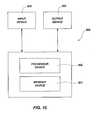
- FIG. 15is a schematic block diagram illustrating one embodiment of an electronic system that includes a semiconductor device including a diode and a conductive strap of the disclosure.
- the diode structureincludes, for example, a conductive strap formed over an insulator material and a diode formed of a single crystalline silicon material formed over the conductive strap.
- the diodemay be a vertical diode structure having a first doped region formed over the conductive strap and a second doped region formed over the first doped region.
- a memory cellmay be formed over the diode.
- Methods of forming such structuresinclude forming a base structure including a second semiconductor substrate having a first doped region and a second doped region, a conductive material, an adhesion material, and an insulator material over a first semiconductor substrate. A portion of the second semiconductor substrate, the conductive material, and the adhesion material may be removed to form the conductive strap and the diode structure.
- the diode structures formed in accordance with the various embodiments of the disclosureare formed of a single crystalline silicon material.
- conventional diodesare formed of a polysilicon material.
- Such conventional diodesexhibit poor I on /I off performance due to the low carrier mobility in the polysilicon material and current leaks, which typically form at the boundaries of the silicon grains.
- the I on /I off performance of the diodemay be improved as the single crystalline silicon material has greater ion mobility than polysilicon material.
- current leaksare less likely to form within the single crystalline silicon material.
- the diodes formed from the single crystalline silicon materialmay be smaller than a diode formed of polysilicon material.
- the methods for forming the diode structures in accordance with various embodiments of the disclosureinclude forming a second semiconductor substrate overlying a conductive material. Because the conductive material, which may be used to form a conductive strap, is buried beneath the second semiconductor substrate, the diode structure may be formed in the second semiconductor substrate in relatively few process acts, as described in greater detail below. For example, in one embodiment, a cross point array including a plurality of diodes having a memory cell formed on each diode may be formed in as few as two patterning and etching acts.
- the diode structuresare formed over the conductive strap, the diode structures may be self-aligned with the conductive strap and, thus, contact resistance caused by misalignment between the diode and the conductive strap may be reduced.
- the memory cell and the diodemay also be self aligned, thus decreasing contact resistance caused by misalignment between the diode and the memory cell.
- the diode structures formed in accordance with various embodiments of the disclosuremay be used to fabricate a variety of semiconductor devices, such as an integrated circuit including a logic device formed in/on the first semiconductor substrate and a memory device including the diode structure formed in/on the second semiconductor substrate. Since a logic device may be formed on the first semiconductor substrate before the memory device including the diode structure is formed, the memory device is not exposed to the processing conditions used for the formation of the logic device. By forming such vertical integrated circuits, the cell size may be reduced, which provides for increased cache memory density.
- the diode structures formed in accordance with various embodiments of the disclosuremay be used to form, for example, flash memory, imagers, and phase change memory (PCRAM).
- PCRAMphase change memory
- the materials described hereinmay be formed by any suitable technique including, but not limited to, spin coating, blanket coating, chemical vapor deposition (“CVD”), plasma enhanced chemical vapor deposition (“PECVD”), atomic layer deposition (“ALD”), plasma enhanced ALD, or physical vapor deposition (“PVD”).
- CVDchemical vapor deposition
- PECVDplasma enhanced chemical vapor deposition
- ALDatomic layer deposition
- PVDphysical vapor deposition
- materialsmay be grown in situ.
- a technique suitable for depositing or growing a particular materialmay be selected by a person of ordinary skill in the art. While the materials described and illustrated herein may be formed as layers, the materials are not limited thereto and may be formed in other three-dimensional configurations.
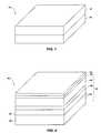
- FIGS. 1 through 8are partial perspective views of a method of forming an embodiment of a semiconductor device 100 ( FIG. 8 ) of the present invention.
- the semiconductor device 100may be formed using a semiconductor structure 34 ( FIG. 4 ), also referred to herein as a base structure 34 , which is formed by bonding an acceptor wafer 10 ( FIG. 1 ) and a donor wafer 16 ( FIG. 2 ). Forming such base structures 34 are described in detail in U.S. patent application Ser. No.
- FIGS. 1 through 4illustrate one example of a method of forming the base structure 34
- any of the methods described in U.S. patent application Ser. No. 12/______, or other known methods,may be utilized to form the base structure 34 .
- FIG. 1depicts the acceptor wafer 10 .
- the acceptor wafer 10may include a first semiconductor substrate 12 having an insulator material 14 formed thereon.
- the first semiconductor substrate 12may include a fabrication substrate, such as a full or partial wafer of semiconductor material (e.g., silicon, gallium arsenide, indium phosphide, etc.), a full or partial silicon-on-insulator (SOI) type substrate, such as a silicon-on-glass (SOG), silicon-on-ceramic (SOC), or silicon-on-sapphire (SOS) substrate, or any other known, suitable fabrication substrate.
- SOIsilicon-on-insulator
- SOIsilicon-on-insulator
- SOIsilicon-on-insulator
- SOIsilicon-on-insulator
- SOIsilicon-on-insulator
- SOIsilicon-on-insulator
- SOIsilicon-on-insulator
- SOIsilicon-on-insulator
- SOIsilicon-on-insulator
- SOIsilicon-
- the first semiconductor substrate 12may be doped or undoped.
- An at least partially fabricated logic devicesuch as a CMOS (complementary metal-oxide semiconductor) device, may optionally be present on the first semiconductor substrate 12 and may be formed by conventional techniques.
- the first semiconductor substrate 12is bulk crystalline silicon.
- the insulator material 14may be a dielectric material including, by way of non-limiting example, silicon dioxide, borophosphosilicate glass (BPSG), borosilicate glass (BSG), phosphosilicate glass (PSG), or the like. In one embodiment, the insulator material 14 is an oxide. The insulator material 14 may be from about 500 ⁇ thick to about 2 ⁇ m thick, such as from about 1000 ⁇ to about 2000 ⁇ . Techniques for deposition and in situ growth of such dielectric materials are known in the art and may include, for example, chemical vapor deposition (CVD), such as low pressure CVD or plasma enhanced CVD, atomic layer deposition (ALD), spin-on deposition, thermal decomposition, or thermal growth.
- CVDchemical vapor deposition
- ALDatomic layer deposition
- spin-on depositionthermal decomposition, or thermal growth.
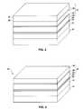
- FIG. 2is a partial perspective view of one embodiment of the donor wafer 16 used to form the base structure 34 ( FIG. 4 ).
- the donor wafer 16may include a precursor semiconductor substrate 18 formed of a single crystalline silicon material.
- a conductive material 20 and an adhesion material 22may be formed over the precursor semiconductor substrate 18 .
- the precursor semiconductor substrate 18may, initially, be doped or undoped.
- the precursor semiconductor substrate 18may initially be a single crystalline silicon material that is undoped or intrinsically doped.
- the precursor semiconductor substrate 18may then be doped, or further doped, to include a first doped region 24 , a second doped region 26 , and a lightly doped region 28 . These doped regions may ultimately form the diode.
- the first doped region 24 and the second doped region 26may be doped with P-type or N-type dopants such that the first doped region 24 and the second doped region 26 are oppositely doped.
- the first doped region 24is an N-type single crystalline silicon material and the second doped region 26 is a P-type single crystalline silicon material.
- the first doped region 24is a P-type single crystalline silicon material and the second doped region 26 is an N-type single crystalline silicon material.
- a lightly doped region 28may be formed between the first doped region 24 and the second doped region 26 .
- the lightly doped region 28may be doped with the same dopant as the second doped region 26 , but the lightly doped region 28 may have a lower concentration of dopant than the second doped region 26 .
- the second doped region 26may be doped with a higher concentration of the P-type dopant and the lightly doped region 28 may be doped with a lower concentration of the P-type dopant.
- a Schottky diodemay be formed at an interface between the first doped region 24 and the conductive material 20 , as known in the art.
- doped regions 24 , 26 , and 28are described as being formed before the donor wafer 16 and acceptor wafer 10 are bonded, doping of the precursor semiconductor substrate 18 to form these regions may be conducted after the donor wafer 16 and the acceptor wafer 10 are bonded.
- the doped regions 24 , 26 , and 28may be formed by a doping technique known in the art, such as diffusion or ion implantation techniques.
- a doping techniqueknown in the art, such as diffusion or ion implantation techniques.
- the first doped region 24may be formed by implanting ions of an N-type impurity, such as arsenic (As), phosphorous (P) or antimony (Sb), into the precursor semiconductor substrate 18 .
- an N-type impuritysuch as arsenic (As), phosphorous (P) or antimony (Sb)
- the second doped region 26is a P-type single crystalline silicon material
- the second doped region 26may be formed by implanting ions of a P-type impurity, such as boron (B), into the precursor semiconductor substrate 18 .
- the depth to which the ions are implanted into the precursor semiconductor substrate 18is at least partially a function of the implant dose and energy.
- the depth of the implanted ions within the precursor semiconductor substrate 18may correspond to a desired thickness of the first doped region 24 and the second doped region 26 .
- the first doped region 24 and the second doped region 26may be formed before or after the conductive material 20 and the adhesion material 22 have been formed on the donor wafer 16 .
- the lightly doped region 28may be doped using the same dopant as the second doped region 26 , except that a lower concentration of the dopant is implanted, such as by adjusting the implant dose or implant energy.
- the conductive material 20may be a low resistivity conductive material including, but not limited to, a phase change material, titanium, titanium silicide, titanium oxide, titanium nitride, tantalum, tantalum silicide, tantalum oxide, tantalum nitride, tungsten, tungsten silicide, tungsten oxide, tungsten nitride, other metals, metal silicide, metal oxide, or metal nitride materials, or combinations thereof, including multiple, different conductive materials.
- the conductive material 20is formed from titanium nitride because titanium nitride has good adherence or adhesion to many materials, such as the single crystalline silicon material used as the precursor semiconductor substrate 18 .
- Titanium nitridealso has a high melting point (about 3000° C.), which makes it unaffected by high processing temperatures. Titanium nitride also makes excellent ohmic contact with other conductive materials. Titanium nitride is also commonly used in semiconductor fabrication and, therefore, may easily be incorporated into conventional fabrication processes.
- the conductive material 20is a titanium-rich titanium nitride, such as metal mode titanium nitride (MMTiN).
- MMTiNmetal mode titanium nitride
- the conductive material 20may also be formed from multiple conductive materials. By way of non-limiting example, the conductive material 20 may be formed from a metal, such as titanium, tungsten or aluminum, with a layer of titanium material formed thereon.
- the thickness of the conductive material 20may be optimized, depending on the material, to provide a low ohmic contact.
- the conductive material 20is titanium nitride, such as MMTiN
- the conductive material 20may have a thickness of from about 10 nm to about 50 nm.
- the conductive material 20may be formed by a deposition technique known in the art, such as, for example, ALD, CVD, or PVD.
- the adhesion material 22may include, for example, an amorphous material, such as an amorphous silicon material or an amorphous germanium material.
- the adhesion material 22may be formed over the conductive material 20 by a deposition technique known in the art, such as, for example, ALD, CVD, or PVD. In one embodiment, the adhesion material 22 may be formed on the conductive material 20 by PVD, followed by chemical-mechanical planarization (CMP).
- CMPchemical-mechanical planarization
- the adhesion material 22may be of sufficient thickness to adhere to the insulator material 14 of the acceptor wafer 10 as described in greater detail below. For example, the thickness of the adhesion material 22 may be from about 10 nm to about 50 nm.
- the donor wafer 16may also include a cleave portion 30 formed by implanting an atomic species into the precursor semiconductor substrate 18 .
- the atomic speciesmay be hydrogen ions, ions of rare gases, also termed inert or noble gases, or ions of fluorine.
- the atomic speciesmay be implanted into the precursor semiconductor substrate 18 of the donor wafer 16 to fowl an implanted zone 32 .
- the atomic speciesmay be implanted into the precursor semiconductor substrate 18 prior to formation of the conductive material 20 thereon, after formation of the conductive material 20 thereon, or after formation of the adhesion material 22 thereon.
- the implanted zone 32may be formed at a desired depth in the precursor semiconductor substrate 18 , which is dependent on parameters such as implant dose and energy of the atomic species, as known in the art.
- the location of the implanted zone 32may correspond to a height of a diode 48 ultimately formed from the precursor semiconductor substrate 18 , as shown in FIG. 7 .
- the implanted zone 32may include microbubbles or microcavities including the implanted atomic species, which provide a weakened region within the precursor semiconductor substrate 18 .
- the donor wafer 16may be thermally treated at a temperature above that at which implantation is effected, but below the melting temperature of the conductive material 20 , to effect crystalline rearrangement in the donor wafer 16 and coalescence of the microbubbles or microcavities.
- the donor wafer 16may be cleaved at the implanted zone 32 , forming the second semiconductor substrate 18 ′ on the base structure 34 ( FIG. 4 ) and cleave portion 30 .
- the term “second semiconductor substrate”is used herein to refer to the semiconductor structure after removal of the cleave portion 30
- the term “precursor semiconductor substrate”is used herein to refer to the semiconductor structure before removal of the cleave portion 30 .
- the donor wafer 16( FIG. 2 ) may be superposed onto the acceptor wafer 10 ( FIG. 1 ) such that the adhesion material 22 of the donor wafer 16 is in contact with the insulator material 14 of the acceptor wafer 10 .
- the adhesion material 22 of the donor wafer 16may then be bonded to the insulator material 14 of the acceptor wafer 10 by exposure to heat.
- at least one of the adhesion material 22 and the insulator material 14may, optionally, be treated to improve the bond strength between the adhesion material 22 and the insulator material 14 .
- Such treatment techniquesare known in the art and may include chemical, plasma, or implant activations.
- the insulator material 14may be treated with a dilute ammonia hydroxide or hydrogen fluoride solution.
- the adhesion material 22may also be exposed to a plasma of, for example, argon, to form a plasma-activated surface. Activating at least one of the adhesion material 22 and the insulator material 14 may increase the kinetics of the subsequent bonding therebetween
- the adhesion material 22 of the donor wafer 16may be contacted and bonded with the insulator material 14 of the acceptor wafer 10 to form a precursor of the base structure 34 ( FIG. 4 ).
- the adhesion material 22may be bonded to the insulator material 14 by, for example, heating the base structure 34 to a temperature of less than about 600° C., such as from about 300° C. to about 400° C. If the insulator material 14 is formed from silicon dioxide, silicon-oxide bonds may form between the adhesion material 22 and the insulator material 14 . Because the conductive material 20 may be formed of a metal or other heat sensitive material, the temperature to which the base structure 34 is exposed may be less than the melting point of the conductive material 20 .
- the adhesion material 22 and the insulator material 14may also be bonded without heat, such as at ambient temperature (from about 20° C. to about 25° C.). Pressure may also be applied to the donor wafer 16 and the acceptor wafer 10 to bond the adhesion material 22 to the insulator material 14 . Once the donor wafer 16 is bonded to the acceptor wafer 10 , the conductive material 20 from the donor wafer 16 may form a buried conductive material, which is disposed between the insulator material 14 and the precursor semiconductor substrate 18 .
- the cleave portion 30may then be removed from the precursor semiconductor substrate 18 to form the base structure 34 shown in FIG. 4 .
- the cleave portion 30may be removed by techniques known in the art, such as by applying a shear force to the implanted zone 32 or by applying heat or a jet gas stream at the implanted zone 32 .
- the hydrogen or other ions implanted in implanted zone 32produce a weakened region in the precursor semiconductor substrate 18 , which is susceptible to cleavage.
- the remaining portion of the precursor semiconductor substrate 18 (second semiconductor substrate 18 ′)may have a thickness, for example, of from about 50 nm to about 500 nm (from about 500 ⁇ to about 5000 ⁇ ).
- the second semiconductor substrate 18 ′ of the base structure 34may be smoothed according to conventional techniques such as, for example, one or more of grinding, wet etching, and chemical-mechanical planarization (CMP).
- the base structure 34may be formed by modification of SMART-CUT® layer transfer technology.
- the SMART-CUT® layer transfer technologyis described in detail in, for example, U.S. Pat. No. RE 39,484 to Bruel, U.S. Pat. No. 6,303,468 to Aspar et al., U.S. Pat. No. 6,335,258 to Aspar et al., U.S. Pat. No. 6,756,286 to Moriceau et al., U.S. Pat. No. 6,809,044 to Aspar et al., U.S. Pat. No. 6,946,365 to Aspar et al., and U.S. Patent Application Publication No.
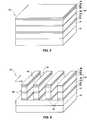
- a bottom electrode 36 , a memory medium 38 , and a top electrode 40may be formed over the second semiconductor substrate 18 ′. If the second semiconductor substrate 18 ′ were not previously doped, as described above, the second semiconductor substrate 18 ′ may be doped prior to forming the bottom electrode 36 , the memory medium 38 , and the top electrode 40 .
- the bottom electrode 36may be formed from a conductive material, such as titanium, titanium silicide, titanium nitride, tungsten, tungsten silicide, tungsten nitride, or combinations thereof.
- the bottom electrode 36is MMTi, titanium, MMTi/titanium nitride, or titanium/titanium nitride.
- the bottom electrode 36may be formed over the second semiconductor substrate 18 ′ using a deposition technique known in the art, such as, for example, ALD, CVD, or PVD.
- the memory medium 38may be formed of any medium capable of holding distinct detectable states.
- the memory medium 38may be formed of a transition metal material, such as nickel oxide or copper oxide, a phase change material, such as a chalcogenide material, or a resistive oxide material.
- the memory medium 38includes a conductive oxide material, a solid electrolyte material, an antifuse oxide material, an ovonic material, or a ferroelectric material.
- the memory medium 38may also be formed by a deposition technique known in the art, such as, ALD, CVD, or PVD.
- the top electrode 40may be formed of a conductive material similar to the bottom electrode 36 .
- a two mask processmay be used to define a cross point array including at least one diode 48 having a memory cell 46 thereon formed over a conductive strap 42 .
- the top electrode 40 , the memory medium 38 , the bottom electrode 36 , the second semiconductor substrate 18 ′, the conductive material 20 , and the adhesion 22 materialmay be patterned using a single mask to form pillars 45 having at least one first trench 44 there between. As shown in FIG.
- the top electrode 40 , the memory medium 38 , the bottom electrode 36 , the second semiconductor substrate 18 ′, the conductive material 20 , and the adhesion material 22may be patterned and etched in a first direction Y, as described in greater detail below.
- the conductive material 20 underlying the pillars 45forms the conductive strap 42 , which may also function as a word line in the semiconductor device 100 ( FIG. 8 ).
- the pillars 45may be formed by depositing a mask material (not shown) over the top electrode 40 and patterning the mask material to form apertures through which surfaces of the top electrode 40 are exposed.
- the mask materialmay include, for example, a photoresist material, an oxide material, transparent carbon, or amorphous carbon. Methods of forming and patterning the mask material are known in the art and, therefore, are not described in detail herein.
- the pattern in the mask materialmay then be transferred to the underlying materials using dry or wet etch techniques.
- an anisotropic reactive ion (i.e., plasma) etching or reactive ion etching (RIE) processmay be used.
- the etch techniquemay be selected by a person of ordinary skill in the art based on the material to be removed. Multiple materials may also be removed simultaneously, depending on the similarity in materials. The techniques for removing the underlying materials are conventional and, therefore, are not described in detail herein.
- the removed portions of the top electrode 40 , the memory medium 38 , the bottom electrode 36 , the second semiconductor substrate 18 ′, the conductive material 20 , and the adhesion material 22may form the at least one first trench 44 .
- the portions of each of the top electrode 40 , the memory medium 38 , the bottom electrode 36 , the second semiconductor substrate 18 ′, the conductive material 20 , and the adhesion material 22 remaining under the mask materialform the pillars 45 .
- the conductive material 20 at the bottom of the pillars 45forms the conductive strap 42 .
- a portion of the insulator material 14may also be etched in order to ensure complete electrical isolation of adjacent conductive straps 42 from one another.
- the remaining portions of the mask material overlying the pillars 45may then be removed.
- the at least one first trench 44may be formed extending in a first direction Y through each of the top electrode 40 , the memory medium 38 , the bottom electrode 36 , the second semiconductor substrate 18 ′, the conductive material 20 , and the adhesion material 22 .
- the top electrode 40 , the bottom electrode 36 , and the conductive material 20are each formed from titanium nitride
- a mixture of bromine-containing gas and a fluorine-containing gas or a mixture of a fluorine-containing gas and a chlorine-containing gasmay be used to remove each of these titanium nitride materials and the adhesion material 22 selective to the mask material and the insulator material 14 .
- the second semiconductor substrate 18 ′may be selectively removed using a reactive ion etching (RIE) process using oxygen (O 2 ) gas and tetrafluoromethane (CF 4 ) gas.
- RIEreactive ion etching
- a fill materialmay be formed in the at least one first trench 44 and subject to CMP so that an upper surface 43 of the base structure 34 is substantially planar.
- the fill materialmay include, for example, a dielectric material such as an oxide material, a nitride material, or a spin-on-glass (SOG) material, and may be deposited using a chemical vapor deposition process.
- portions of the top electrode 40 , the memory medium 38 , the bottom electrode 36 , and the second semiconductor substrate 18 ′may be patterned using a second mask to form at least one diode 48 having a memory cell 46 formed thereon.
- the diode 48includes the first doped region 24 , the lightly doped region 28 , and the second doped region 26 .
- the memory cell 46includes the bottom electrode 36 , the memory medium 38 , and the top electrode 40 .
- At least one second trench 47may be formed between adjacent diodes 48 over a common conductive strap 42 .
- the lightly doped region 28 and a portion of the first doped region 24may be patterned and etched in a second direction X to form at least one second trench 47 , as described in greater detail below.
- the second direction Xmay be substantially perpendicular to the first direction Y.
- the diode 48is self-aligned with the conductive strap 42 thus eliminating the need for a separate electrical contact between the diode 48 and the conductive strap 42 .
- each diode 48may be from about 2:1 to about 20:1 and, more particularly, from about 5:1 to about 10:1.
- the width of each diode 48may be from about 5 nm to about 50 nm and, more particularly, from about 10 nm to about 20 nm. Because the diode 48 is formed of a single crystalline silicon material rather than a polysilicon material, the diode 48 may have a smaller width and height than a diode formed of polysilicon material.
- diodes formed of a polysilicon materialhave a lower carrier mobility than and experience a greater occurrence of leaks along the grain boundary, thus providing a lower performance than a diode formed of a single crystal silicon material. Additionally, because the diode 48 is formed of a single crystalline silicon material, the diode 48 may have a greater ability to transfer ions than a diode formed from polysilicon and, therefore, will have a greater I on /I off performance than a polysilicon diode.
- Each diode 48 and memory cell 46may be formed by depositing a mask material (not shown) over the top electrode 40 and the fill material (not shown) and patterning the mask material to form apertures through which surfaces of the top electrode 40 are exposed.
- surfaces of the fill material (not shown)may also be exposed through the mask material.
- the mask materialmay include, for example, a photoresist material, an oxide material, transparent carbon or amorphous carbon. Methods of forming and patterning the mask material are known in the art and, therefore, are not described in detail herein.
- Portions of the top electrode 40 , the memory medium 38 , the bottom electrode 36 , and the second semiconductor substrate 18 ′ including the second doped region 26 , the partially doped region 28 , and a portion of the first doped region 24 that are exposed through the apertures in the mask materialmay be removed to fowl each diode 48 and memory cell 46 .
- the top electrode 40 and the bottom electrode 26are each formed from titanium nitride
- a mixture of bromine-containing gas and a fluorine-containing gas or a mixture of a fluorine-containing gas and a chlorine-containing gasmay be used to remove each of the titanium nitride materials selective to the mask material and the insulator material 14 .
- the second semiconductor substrate 18 ′may be selectively removed using a reactive ion etching (RIE) process using oxygen (O 2 ) gas and tetrafluoromethane (CF 4 ) gas.
- RIEreactive ion etching
- An additional fill materialmay be formed in any etched portions of the at least one first trench 44 and the at least one second trench 47 and subject to CMP so that the upper surface 43 of the base structure 34 and the fill material are substantially planar with one another.
- At least one bit line 50may be formed over the top electrode 40 of the memory cell 46 .
- the at least one bit line 50may electrically couple more than one of the memory cell 46 .
- the bit line 50may extend in the second direction X over adjacent memory cells 46 , electrically coupling memory cells 46 on at least two distinct conductive straps 42 .
- the bit line 50may be formed by depositing a conductive material over the semiconductor base 34 ( FIG. 7 ) and patterning the conductive material to form substantially straight and substantially parallel bit lines 50 .
- the bit line 50may patterned and etched, as known in the art, in the second direction X to expose the at least one second trench 47 .
- the resulting semiconductor device 100 shown in FIG. 8includes a cross-point diode memory array including the first semiconductor substrate 12 , the insulator material 14 , the adhesion material 22 bonded to the insulator material 14 , the conductive material 20 over the adhesion material 22 , wherein the conductive material 20 and the adhesion material 22 form at least two conductive straps 42 , a plurality of diodes 48 formed over the at least two conductive straps 42 , a memory cell 46 formed on each of the plurality of diodes 48 , and a bit line 50 formed over the memory cells 46 .
- FIGS. 9-14illustrate another method of forming a semiconductor device 200 ( FIG. 14 ) of the present invention.
- FIG. 9illustrates a base structure 34 , which is a substantial duplication of FIG. 4 and may be formed as described above regarding FIGS. 1-4 .
- the base structure 34includes a first semiconductor substrate 12 , an insulator material 14 , an adhesion material 22 , a conductive material 20 , and a second semiconductor substrate 18 ′ including a first doped region 24 , a lightly doped region 28 , and a second doped region 26 .
- a bottom electrode 52may be formed over the second semiconductor substrate 18 ′. If the second semiconductor substrate 18 ′ was not previously doped, as described above, the second semiconductor substrate 18 ′ may be doped prior to forming the bottom electrode 52 .
- the bottom electrode 52may be formed from a conductive material, such as titanium, titanium silicide, titanium nitride, tungsten, tungsten silicide, tungsten nitride, or combinations thereof.
- the bottom electrode 52is MMTi, titanium, MMTi/titanium nitride, or titanium/titanium nitride.
- the bottom electrode 52may be formed on the second semiconductor substrate 18 ′ using a deposition technique known in the art, such as, for example, ALD, CVD, or PVD.
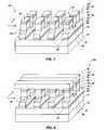
- a two mask processmay be used to define a cross point array including at least one diode 62 having a bottom electrode 52 thereon formed over a conductive strap 54 .
- the bottom electrode 52 , the second semiconductor substrate 18 ′, the conductive material 20 , and the adhesion material 22may be removed using a first mask to form pillars 58 having trenches 56 there between.
- the bottom electrode 52 , the second semiconductor substrate 18 ′, the conductive material 20 , and the adhesion material 22may be patterned and etched in a first direction Y as described in greater detail below.
- the conductive material 20 underlying the pillars 58forms the conductive strap 54 , which may also function as a word line in the semiconductor device 200 ( FIG. 14 ).
- the pillars 58may be formed by depositing a mask material (not shown) over the bottom electrode 52 and patterning the mask material to form apertures through which surfaces of the bottom electrode 52 are exposed.
- the mask materialmay include, for example, a photoresist material, an oxide material, transparent carbon or amorphous carbon. Methods of forming and patterning the mask material are known in the art and, therefore, are not described in detail herein.
- the pattern in the mask materialmay then be transferred to the underlying materials using dry or wet etch techniques.
- an anisotropic reactive ion (i.e., plasma) etching or reactive ion etching (RIE) processmay be used.
- the etch techniquemay be selected by a person of ordinary skill in the art based on the material to be removed. Multiple materials may also be removed simultaneously, depending on the similarity in materials. The techniques for removing the underlying materials are conventional and, therefore, are not described in detail herein.
- the removed portions of the bottom electrode 52 , the second semiconductor substrate 18 ′, the conductive material 20 , and the adhesion material 22may form the trenches 56 .
- the portions of each of the bottom electrode 52 , the second semiconductor substrate 18 ′, the conductive material 20 , and the adhesion material 22 remaining under the mask materialform the pillars 58 .
- the conductive material 20 at the bottom of the pillars 58forms the conductive strap 54 .
- a portion of the insulator material 14may also be etched in order to ensure complete electrical isolation of adjacent conductive straps 54 from one another. The remaining portions of the mask material overlying the pillars 58 may then be removed.
- the trenches 56may be formed extending in a first direction Y through each of the bottom electrode 52 , the second semiconductor substrate 18 ′, the conductive material 20 , and the adhesion material 22 .
- the bottom electrode 52 and the conductive material 20are each formed from titanium nitride
- a mixture of bromine-containing gas and a fluorine-containing gas or a mixture of a fluorine-containing gas and a chlorine-containing gasmay be used to selectively remove each of these titanium nitride materials and the adhesion material 22 selective to the mask material and the insulator material 14 .
- the second semiconductor substrate 18 ′may be selectively removed using a reactive ion etching (RIE) process using oxygen (O 2 ) gas and tetrafluoromethane (CF 4 ) plasma.
- a fill material(not shown) may be formed in the trenches 56 and subject to CMP so than an upper surface 60 of the semiconductor base 34 is substantially planar.
- the fill materialmay include, for example, a dielectric material such as an oxide material, a nitride material, or a spin-on-glass (SOG) material, and may be deposited using a chemical vapor deposition process.
- portions of the bottom electrode 52 and the second semiconductor substrate 18 ′may be removed using a second mask to form at least one diode 62 having the bottom electrode 52 formed thereon.
- a trench 64may be formed between adjacent diodes 62 over a common conductive strap 54 .
- the bottom electrode 52 and the second semiconductor substrate 18 ′ including the second doped region 26the lightly doped region 28 and a portion of the first doped region 24 may be patterned and etched in a second direction X to form the trench 64 as described in greater detail below.
- the second direction Xmay be substantially perpendicular to the first direction Y.
- each diode 62is self aligned with the conductive strap 54 , thus eliminating the need for a separate electrical contact between the diode 62 and the conductive strap 54 .
- the aspect ratio of each diode 62may be from about 5:1 to about 40:1 and, more particularly, from about 20:1 to about 30:1.
- the width of each diode 62may be about 5 nm to about 40 nm and, more particularly, from about 10 nm to about 20 nm. Because the diode 62 is formed of a single crystalline silicon material rather than a polysilicon material, the diode 62 may have a smaller width and height than a diode formed of polysilicon material.
- the diode 62is formed of a single crystalline silicon material, the diode 62 may have a greater ability to transfer ions than a diode formed from polysilicon, and, therefore, will have a greater I on /I off performance than a polysilicon diode.
- Each diode 62may be formed by depositing a mask material (not shown) over the bottom electrode 52 and the fill material (not shown) and patterning the mask material to form apertures through which surfaces of the bottom electrode 52 are exposed.
- surfaces of the fill material (not shown)may also be exposed through the mask material.
- the mask materialmay include, for example, a photoresist material, an oxide material, transparent carbon or amorphous carbon. Methods of forming and patterning the mask material are known in the art and, therefore, are not described in detail herein.
- Portions of the bottom electrode 52 and the second semiconductor substrate 18 ′ including the second doped region 26 , the partially doped region 28 , and a portion of the first doped region 24 that are exposed through the apertures in the mask materialmay be removed to form each diode 62 having the bottom electrode 52 formed thereon.
- the bottom electrode 52is formed from titanium nitride
- a mixture of bromine-containing gas and a fluorine-containing gas or a mixture of a fluorine-containing gas and a chlorine-containing gasmay be used to selectively remove the titanium nitride materials selective to the mask material and the insulator material 14 .
- the second semiconductor substrate 18 ′may be selectively removed using a reactive ion etching (RIE) process using oxygen (O 2 ) gas and tetrafluoromethane (CF 4 ) gas.
- RIEreactive ion etching
- An additional fill materialmay be formed in any etched portions of the trenches 56 and the trenches 64 and subject to CMP so that the upper surface 60 of the semiconductor structure and the fill material are substantially planar with one another.
- a memory medium 66may be formed over the bottom electrode 52 .
- the memory medium 66may be formed of any medium known in the art capable of holding a distinct detectable state or holding a charge.
- the memory medium 66may be formed of a phase change or resistant material such as a chalcogenide material.
- Additional examples of the memory medium 66include a conductive oxide material, a solid electrolyte material, an antifuse oxide material, an ovonic material, and a ferroelectric material.
- the memory medium 66may be formed by a deposition technique known in the art, such as, for example ALD, CVD, or PVD. In one embodiment, the memory medium 66 may be blanket deposited over the upper surface 60 ( FIGS. 11 and 12 ) of the semiconductor structure. The memory medium 66 may then be patterned and etched as known in the art and as previously described herein such that the memory medium 66 is formed over each of the bottom electrodes 52 .
- At least one bit line 68may be formed over the memory medium 66 .
- the bit line 68may act as both a bit line and a top electrode.
- the bottom electrode 52 , the memory medium 66 , and the bit line 68may form a memory cell 70 .
- the at least one bit line 68may electrically couple more than one memory cell 70 .
- the bit line 68may extend in the second direction X over adjacent memory cells 70 , electrically coupling memory cells 70 on two distinct conductive straps 54 .
- the bit line 68may be formed by depositing a conductive material over the base structure 34 and patterning the conductive material to form substantially straight and substantially parallel bit lines 68 .
- a fill material(not shown) may be deposited in the trenches 56 and the trenches 64 as previously described and the bit line 68 may be blanket deposited over the pillars 58 and the fill material. The bit line 68 may then be patterned and etched, as known in the art, in the second direction X to expose the trenches 64 .
- the resulting semiconductor device 200 shown in FIG. 14includes a cross-point diode memory array including the first semiconductor substrate 12 , the insulator material 14 , the adhesion material 22 bonded to the insulator material 14 , the conductive material 20 over the adhesion material 22 , wherein the conductive material 20 and the adhesion material 22 form at least two conductive straps 54 , a plurality of diodes 62 formed over the at least two conductive straps 54 , memory cells 70 formed on each of the plurality of diodes 62 , wherein the top electrode of the memory cell 70 is the bit line 68 .
- the semiconductor device 200 formed according to FIGS. 9-14may be substantially similar to the semiconductor device 100 formed according to FIGS. 1-8 with the exception that in the semiconductor device 200 , the bit line 68 is the top electrode of the memory cell 70 while in the semiconductor device 100 , the bit line 50 is electrically coupled to the top electrode 40 of the memory cell 46 .
- FIG. 15is a block diagram of an illustrative electronic system 300 according to the present invention.
- the electronic system 300may include, for example, a computer or computer hardware component, a server or other networking hardware component, a cellular telephone, a digital camera, a personal digital assistant (PDA), portable media (e.g., music) player, etc.
- the electronic system 300includes at least one memory device 301 .
- the electronic system 300may further include at least one electronic signal processor device 302 (often referred to as a “microprocessor”).
- At least one of the electronic signal processor device 302 and the at least one memory device 301may include, for example, an embodiment of the semiconductor device 100 , 200 described above.
- at least one of the electronic signal processor device 302 and the at least one memory device 301may include an embodiment of a semiconductor device including a diode structure over a conductive material as previously described in relation to the semiconductor devices 100 , 200 shown in FIGS. 8 and 14 , respectively.
- the electronic system 300may further include one or more input devices 304 for inputting information into the electronic system 300 by a user, such as, for example, a mouse or other pointing device, a keyboard, a touchpad, a button, or a control panel.
- the electronic system 300may further include one or more output devices 306 for outputting information (e.g., visual or audio output) to a user such as, for example, a monitor, a display, a printer, an audio output jack, a speaker, etc.
- the input device 304 and the output device 306may include a single touchscreen device that can be used both to input information to the electronic system 300 and to output visual information to a user.
- the one or more input devices 304 and output devices 306may communicate electrically with at least one of the memory device 301 and the electronic signal processor device 302 .
- the present inventionincludes semiconductor devices including diode structures having a conductive strap and methods for forming such devices.
- Such devicesmay include a conductive material over an insulator material, at least one diode comprising a single crystalline silicon material over the conductive material, the diode having a first doped region overlying the conductive material and a second doped region overlying the first doped region wherein the conductivity of the first doped region is opposite the conductivity of the second doped region, and a memory cell over the second doped region.
- the memory cellmay include a bottom electrode, a memory medium, and a top electrode.
- the top electrodemay be a bit line. In other embodiments, a bit line may be electrically coupled to the memory cell.
- the present inventionincludes a semiconductor device that includes an insulator material on a first semiconductor substrate, an adhesion material bonded to the insulator material, a conductive material over the adhesion material, wherein the conductive material and the adhesion material are patterned to form at least one conductive strap, at least one diode over the conductive strap, and a memory cell on the at least one diode.
- the conductive strapmay comprise a word line.
- the present inventionincludes a semiconductor device including a first semiconductor substrate having an insulator material thereon, an adhesion material bonded to the insulator material, a conductive material over the adhesion material, wherein the conductive material and the adhesion material are patterned to form at least two conductive straps, a plurality of diodes on each of the at least two conductive straps, each diode comprising a single crystalline silicon material, and a plurality of memory cells, one memory cell of the plurality of memory cells being on each of the plurality of diodes.
- the present inventionincludes methods for fabricating a semiconductor device that include forming a base comprising a second semiconductor substrate comprising a single crystalline silicon material having a first doped region and a second doped region, a conductive material, an adhesion material, and an insulator material overlying a first semiconductor substrate, forming a top electrode, a memory medium, and a bottom electrode over the second semiconductor substrate, removing a portion of the top electrode, the memory medium, the bottom electrode, the second semiconductor substrate, the conductive material, and the adhesion material to form at least one conductive strap having a pillar of the top electrode, the memory medium, the bottom electrode and the second semiconductor substrate thereon, and removing another portion of the top electrode, the memory medium, the bottom electrode, and the second semiconductor substrate to form at least one diode over the at least one conductive strap having a memory cell on the at least one diode.
- the present inventionincludes methods of forming a semiconductor device that include forming a base comprising a second semiconductor substrate comprising a single crystalline silicon material having a first doped region and a second doped region, a conductive material, an adhesion material, and an insulator material overlying a first semiconductor substrate, forming a bottom electrode over the second semiconductor substrate, removing a portion of the bottom electrode, the second semiconductor substrate, the conductive material, and the adhesion material to form at least one conductive strap having a pillar of the bottom electrode and the second semiconductor substrate thereon, and removing another portion of the bottom electrode, and the second semiconductor substrate to form at least one diode over the at least one conductive strap having a portion of the bottom electrode on the at least one diode, forming a memory medium over each portion of the bottom electrode, and forming at bit line over the memory medium.
Landscapes
- Engineering & Computer Science (AREA)
- Manufacturing & Machinery (AREA)
- Physics & Mathematics (AREA)
- Condensed Matter Physics & Semiconductors (AREA)
- General Physics & Mathematics (AREA)
- Computer Hardware Design (AREA)
- Microelectronics & Electronic Packaging (AREA)
- Power Engineering (AREA)
- Semiconductor Memories (AREA)
Abstract
Description
- The present application is related to co-pending U.S. patent application Ser. No. 12/______ filed on even date herewith and titled “SEMICONDUCTOR-METAL-ON-INSULATOR STRUCTURES, METHODS OF FORMING SUCH STRUCTURES, AND SEMICONDUCTOR DEVICES INCLUDING SUCH STRUCTURES” (attorney docket number 2269-9742US); co-pending U.S. patent application Ser. No. 12/______ filed on even date herewith and titled “FLOATING BODY CELL STRUCTURES, DEVICES INCLUDING SAME AND METHODS FOR FORMING SAME (attorney docket number 2269-9743US); co-pending U.S. patent application Ser. No. 12/______ filed on even date herewith and titled “THYRISTOR-BASED MEMORY CELLS, DEVICES AND SYSTEMS INCLUDING THE SAME AND METHODS FOR FORMING THE SAME” (attorney docket number 2269-9804US); and co-pending U.S. patent application Ser. No. 12/______ filed on even date herewith and titled “SEMICONDUCTOR CELLS, ARRAYS, DEVICES AND SYSTEMS HAVING A BURIED CONDUCTIVE LINE AND METHODS FOR FORMING SAME” (attorney docket number 2269-9819US), the disclosure of each of which is incorporated herein in its entirety by reference.
- The present invention, in various embodiments, relates generally to semiconductor structures including a diode and methods of forming such semiconductor structures. More specifically, embodiments of the present invention relate to a diode structure having a conductive strap, devices including such a diode structure, and methods of forming such a diode structure.
- One of the common trends in the electronics industry is the miniaturization of electronic devices. This is especially true for electronic devices operated through the use of semiconductor microchips. Microchips are commonly viewed as the so-called “brains” of most electronic devices. In general, a microchip comprises a small silicon wafer upon which are built thousands of microscopic electronic devices that are integrally configured to form electronic circuits. The circuits are interconnected in a unique way to perform a desired function.
- With the desire to decrease the size of electronic devices, it is also necessary to decrease the size of the microchip and electronic devices thereon. This movement has increased the number and complexity of circuits on a single microchip.
- Conventionally, electronic devices are formed side-by-side in a single plane on a common substrate, such as a silicon wafer. This side-by-side positioning, however, uses a relatively large amount of surface area or so-called “real estate” on the substrate. As a result, larger substrates are required.
- A recent trend is to vertically stack semiconductor devices on a single substrate. However, the stacking of semiconductor devices adds an additional degree of complexity to arranging the components of the semiconductor device. Furthermore, the processing conditions for fabrication of stacked or superimposed devices must be controlled so as not to damage components in underlying devices. In addition to stacking semiconductor devices, individual devices may be formed having high aspect ratios (i.e., the ratio of height to width). However, these high aspect ratios can increase the risk of the breakage of the device because of the limited surface area of the bond between the device to the substrate. Similarly, as the size of the devices decrease, interconnects, such as bit lines and word lines, may also need to decrease in size, e.g., width. In some cases, the size of the device may be so small that it becomes impractical, if not impossible, to form interconnects of the desired size on the device.
- One common type of electronic device found on a microchip is a diode. A diode functions as a type of electrical gate or switch. An ideal diode will allow an electrical current to flow through the diode in one direction but will not allow the electrical current to flow through the diode in the opposite direction. In conventional diodes, however, a small amount of current flows in the opposite direction. This is referred to as current leakage.
- Conventional diodes are typically formed from a silicon material that is modified through a doping process. Doping is a process in which ions are diffused or implanted within the silicon and then activated. There are two general types of dopants: P-type dopants and N-type dopants. P-type dopants produce positive charged holes. In contrast, N-type dopants produce extra electrons with negative charges. In general, a semiconductor diode is formed when a material doped with a P-type dopant is placed adjacent to a material with an N-type dopant.
- Conventionally, diodes are configured by positioning the two opposing doped materials side-by-side on a microchip. This side-by-side positioning, however, uses a relatively large amount of surface area on a microchip. As a result, larger microchips are required.
- Furthermore, for a diode to operate, each side of the diode must have an electrical connection that either brings electricity to or from the diode. The minimal size of each side of the diode is in part limited in that each side must be large enough to accommodate an electrical connection. Since conventional diodes have a side-by-side configuration with each side requiring a separate electrical connection, the ability to miniaturize such diodes is limited. In addition, the requirement of having side-by-side electrical connections on a single diode increases the size and complexity of the microchip.
- In order to rectify some of these shortcomings, various attempts have been made to form a vertical diode structure. For example, U.S. patent application Ser. No. 12/434,212 to Gonzalez et al. titled Method of Making Semiconductor Structures Including Vertical Diode Structures, hereinafter referred to as “Gonzalez” and the disclosure of which is incorporated herein in its entirety by reference, describes one method of making a vertical diode structure. However, such vertical diode structures are formed using a polysilicon material which has a poor Ion/Ioffperformance due to the low carrier mobility through the polysilicon material. Current leaks may also form at a grain boundary of the polysilicon material, thus also decreasing the Ion/Ioffperformance of the diode. The method of farming such vertical diodes, as described in Gonzalez, also does not provide an adequate means of forming an electrical contact for the diode when the diode is miniaturized, such as when the width of the diode is less than about 20 nm.
- Accordingly, there is a need for a method of forming a vertical semiconductor device including a diode which provides high Ion/Ioffperformance and provides for easy accessibility of an electrical contact, such as a conductive strap, to the diode. Additionally, there is a need for a method of forming such diodes as part of a semiconductor device wherein the diode may be formed over a first electronic device without damaging the first electronic device.
FIGS. 1-8 are partial perspective views of a semiconductor device including a diode and a conductive strap during various processing acts in accordance with one embodiment of the disclosure;FIGS. 9-14 are partial perspective views of a semiconductor device including a diode and a conductive strap during various processing acts in accordance with one embodiment of the disclosure; andFIG. 15 is a schematic block diagram illustrating one embodiment of an electronic system that includes a semiconductor device including a diode and a conductive strap of the disclosure.- A diode structure over a conductive strap, devices including such structures, and methods of forming such a structure are disclosed. The diode structure includes, for example, a conductive strap formed over an insulator material and a diode formed of a single crystalline silicon material formed over the conductive strap. The diode may be a vertical diode structure having a first doped region formed over the conductive strap and a second doped region formed over the first doped region. A memory cell may be formed over the diode. Methods of forming such structures include forming a base structure including a second semiconductor substrate having a first doped region and a second doped region, a conductive material, an adhesion material, and an insulator material over a first semiconductor substrate. A portion of the second semiconductor substrate, the conductive material, and the adhesion material may be removed to form the conductive strap and the diode structure.
- The diode structures formed in accordance with the various embodiments of the disclosure are formed of a single crystalline silicon material. In contrast, conventional diodes are formed of a polysilicon material. Such conventional diodes exhibit poor Ion/Ioffperformance due to the low carrier mobility in the polysilicon material and current leaks, which typically form at the boundaries of the silicon grains. By forming the diode from a single crystalline silicon material, the Ion/Ioffperformance of the diode may be improved as the single crystalline silicon material has greater ion mobility than polysilicon material. In addition, current leaks are less likely to form within the single crystalline silicon material. Additionally, because single crystalline silicon material is stronger than polysilicon material, the diodes formed from the single crystalline silicon material may be smaller than a diode formed of polysilicon material.
- The methods for forming the diode structures in accordance with various embodiments of the disclosure include forming a second semiconductor substrate overlying a conductive material. Because the conductive material, which may be used to form a conductive strap, is buried beneath the second semiconductor substrate, the diode structure may be formed in the second semiconductor substrate in relatively few process acts, as described in greater detail below. For example, in one embodiment, a cross point array including a plurality of diodes having a memory cell formed on each diode may be formed in as few as two patterning and etching acts. Furthermore, because the diode structures are formed over the conductive strap, the diode structures may be self-aligned with the conductive strap and, thus, contact resistance caused by misalignment between the diode and the conductive strap may be reduced. The memory cell and the diode may also be self aligned, thus decreasing contact resistance caused by misalignment between the diode and the memory cell.
- The diode structures formed in accordance with various embodiments of the disclosure may be used to fabricate a variety of semiconductor devices, such as an integrated circuit including a logic device formed in/on the first semiconductor substrate and a memory device including the diode structure formed in/on the second semiconductor substrate. Since a logic device may be formed on the first semiconductor substrate before the memory device including the diode structure is formed, the memory device is not exposed to the processing conditions used for the formation of the logic device. By forming such vertical integrated circuits, the cell size may be reduced, which provides for increased cache memory density. The diode structures formed in accordance with various embodiments of the disclosure may be used to form, for example, flash memory, imagers, and phase change memory (PCRAM).
- The following description provides specific details, such as material types and processing conditions, in order to provide a thorough description of embodiments of the present invention. However, a person of ordinary skill in the art will understand that the embodiments of the present invention may be practiced without employing these specific details and in conjunction with conventional fabrication techniques. In addition, the description provided herein does not form a complete process flow for manufacturing a semiconductor device including the diode structure. Only those process acts and structures necessary to understand the embodiments of the present invention are described in detail below. Additional acts to form a complete semiconductor device including the diode structure according to an embodiment of the invention may be performed by conventional techniques.
- The materials described herein may be formed by any suitable technique including, but not limited to, spin coating, blanket coating, chemical vapor deposition (“CVD”), plasma enhanced chemical vapor deposition (“PECVD”), atomic layer deposition (“ALD”), plasma enhanced ALD, or physical vapor deposition (“PVD”). Alternatively, materials may be grown in situ. A technique suitable for depositing or growing a particular material may be selected by a person of ordinary skill in the art. While the materials described and illustrated herein may be formed as layers, the materials are not limited thereto and may be formed in other three-dimensional configurations.
- In the following detailed description, reference is made to the accompanying drawings, which form a part hereof, and in which is shown, by way of illustration, specific embodiments in which the invention may be practiced. These embodiments are described in sufficient detail to enable a person of ordinary skill in the art to practice the invention. However, other embodiments may be utilized, and structural, logical, and electrical changes may be made without departing from the scope of the invention. The illustrations presented herein are not meant to be actual views of any particular system, logic device, memory cell, or semiconductor device, but are merely idealized representations which are employed to describe the present invention. The drawings presented herein are not necessarily drawn to scale. Additionally, elements common between drawings may retain the same numerical designation.
- Referring now to the drawings, where like elements are designated by like reference numerals,
FIGS. 1 through 8 are partial perspective views of a method of forming an embodiment of a semiconductor device100 (FIG. 8 ) of the present invention. The semiconductor device100 (FIG. 8 ) may be formed using a semiconductor structure34 (FIG. 4 ), also referred to herein as abase structure 34, which is formed by bonding an acceptor wafer10 (FIG. 1 ) and a donor wafer16 (FIG. 2 ). Formingsuch base structures 34 are described in detail in U.S. patent application Ser. No. 12/______ filed on even date herewith and titled “SEMICONDUCTOR-METAL-ON-INSULATOR STRUCTURES, METHODS OF FORMING SUCH STRUCTURES, AND SEMICONDUCTOR DEVICES INCLUDING SUCH STRUCTURES” (attorney docket number 2269-9742US). WhileFIGS. 1 through 4 illustrate one example of a method of forming thebase structure 34, any of the methods described in U.S. patent application Ser. No. 12/______, or other known methods, may be utilized to form thebase structure 34. FIG. 1 depicts theacceptor wafer 10. Theacceptor wafer 10 may include afirst semiconductor substrate 12 having aninsulator material 14 formed thereon. Thefirst semiconductor substrate 12 may include a fabrication substrate, such as a full or partial wafer of semiconductor material (e.g., silicon, gallium arsenide, indium phosphide, etc.), a full or partial silicon-on-insulator (SOI) type substrate, such as a silicon-on-glass (SOG), silicon-on-ceramic (SOC), or silicon-on-sapphire (SOS) substrate, or any other known, suitable fabrication substrate. As used herein, the term “wafer” includes conventional wafers as well as other bulk semiconductor substrates. Thefirst semiconductor substrate 12 may be doped or undoped. An at least partially fabricated logic device (not shown), such as a CMOS (complementary metal-oxide semiconductor) device, may optionally be present on thefirst semiconductor substrate 12 and may be formed by conventional techniques. In one embodiment, thefirst semiconductor substrate 12 is bulk crystalline silicon.- The
insulator material 14 may be a dielectric material including, by way of non-limiting example, silicon dioxide, borophosphosilicate glass (BPSG), borosilicate glass (BSG), phosphosilicate glass (PSG), or the like. In one embodiment, theinsulator material 14 is an oxide. Theinsulator material 14 may be from about 500 Å thick to about 2 μm thick, such as from about 1000 Å to about 2000 Å. Techniques for deposition and in situ growth of such dielectric materials are known in the art and may include, for example, chemical vapor deposition (CVD), such as low pressure CVD or plasma enhanced CVD, atomic layer deposition (ALD), spin-on deposition, thermal decomposition, or thermal growth. FIG. 2 is a partial perspective view of one embodiment of thedonor wafer 16 used to form the base structure34 (FIG. 4 ). Thedonor wafer 16 may include aprecursor semiconductor substrate 18 formed of a single crystalline silicon material. Aconductive material 20 and anadhesion material 22 may be formed over theprecursor semiconductor substrate 18. Theprecursor semiconductor substrate 18 may, initially, be doped or undoped. By way of example, theprecursor semiconductor substrate 18 may initially be a single crystalline silicon material that is undoped or intrinsically doped. Theprecursor semiconductor substrate 18 may then be doped, or further doped, to include a firstdoped region 24, a seconddoped region 26, and a lightly dopedregion 28. These doped regions may ultimately form the diode. The firstdoped region 24 and the seconddoped region 26 may be doped with P-type or N-type dopants such that the firstdoped region 24 and the seconddoped region 26 are oppositely doped. For example, in one embodiment, the firstdoped region 24 is an N-type single crystalline silicon material and the seconddoped region 26 is a P-type single crystalline silicon material. Alternatively, in another embodiment, the firstdoped region 24 is a P-type single crystalline silicon material and the seconddoped region 26 is an N-type single crystalline silicon material. A lightly dopedregion 28 may be formed between the firstdoped region 24 and the seconddoped region 26. The lightly dopedregion 28 may be doped with the same dopant as the seconddoped region 26, but the lightly dopedregion 28 may have a lower concentration of dopant than the seconddoped region 26. For example, the seconddoped region 26 may be doped with a higher concentration of the P-type dopant and the lightly dopedregion 28 may be doped with a lower concentration of the P-type dopant. If the firstdoped region 24 is an N-type single crystalline silicon material, a Schottky diode may be formed at an interface between the firstdoped region 24 and theconductive material 20, as known in the art. While the dopedregions donor wafer 16 andacceptor wafer 10 are bonded, doping of theprecursor semiconductor substrate 18 to form these regions may be conducted after thedonor wafer 16 and theacceptor wafer 10 are bonded.- The doped
regions doped region 24 is an N-type single crystalline silicon material, the firstdoped region 24 may be formed by implanting ions of an N-type impurity, such as arsenic (As), phosphorous (P) or antimony (Sb), into theprecursor semiconductor substrate 18. If the seconddoped region 26 is a P-type single crystalline silicon material, the seconddoped region 26 may be formed by implanting ions of a P-type impurity, such as boron (B), into theprecursor semiconductor substrate 18. As known in the art, the depth to which the ions are implanted into theprecursor semiconductor substrate 18 is at least partially a function of the implant dose and energy. The depth of the implanted ions within theprecursor semiconductor substrate 18 may correspond to a desired thickness of the firstdoped region 24 and the seconddoped region 26. The firstdoped region 24 and the seconddoped region 26 may be formed before or after theconductive material 20 and theadhesion material 22 have been formed on thedonor wafer 16. The lightly dopedregion 28 may be doped using the same dopant as the seconddoped region 26, except that a lower concentration of the dopant is implanted, such as by adjusting the implant dose or implant energy. - The
conductive material 20 may be a low resistivity conductive material including, but not limited to, a phase change material, titanium, titanium silicide, titanium oxide, titanium nitride, tantalum, tantalum silicide, tantalum oxide, tantalum nitride, tungsten, tungsten silicide, tungsten oxide, tungsten nitride, other metals, metal silicide, metal oxide, or metal nitride materials, or combinations thereof, including multiple, different conductive materials. In one embodiment, theconductive material 20 is formed from titanium nitride because titanium nitride has good adherence or adhesion to many materials, such as the single crystalline silicon material used as theprecursor semiconductor substrate 18. Titanium nitride also has a high melting point (about 3000° C.), which makes it unaffected by high processing temperatures. Titanium nitride also makes excellent ohmic contact with other conductive materials. Titanium nitride is also commonly used in semiconductor fabrication and, therefore, may easily be incorporated into conventional fabrication processes. In one embodiment, theconductive material 20 is a titanium-rich titanium nitride, such as metal mode titanium nitride (MMTiN). Theconductive material 20 may also be formed from multiple conductive materials. By way of non-limiting example, theconductive material 20 may be formed from a metal, such as titanium, tungsten or aluminum, with a layer of titanium material formed thereon. The thickness of theconductive material 20 may be optimized, depending on the material, to provide a low ohmic contact. For example, if theconductive material 20 is titanium nitride, such as MMTiN, theconductive material 20 may have a thickness of from about 10 nm to about 50 nm. Theconductive material 20 may be formed by a deposition technique known in the art, such as, for example, ALD, CVD, or PVD. - The
adhesion material 22 may include, for example, an amorphous material, such as an amorphous silicon material or an amorphous germanium material. Theadhesion material 22 may be formed over theconductive material 20 by a deposition technique known in the art, such as, for example, ALD, CVD, or PVD. In one embodiment, theadhesion material 22 may be formed on theconductive material 20 by PVD, followed by chemical-mechanical planarization (CMP). Theadhesion material 22 may be of sufficient thickness to adhere to theinsulator material 14 of theacceptor wafer 10 as described in greater detail below. For example, the thickness of theadhesion material 22 may be from about 10 nm to about 50 nm. - The
donor wafer 16 may also include acleave portion 30 formed by implanting an atomic species into theprecursor semiconductor substrate 18. The atomic species may be hydrogen ions, ions of rare gases, also termed inert or noble gases, or ions of fluorine. The atomic species may be implanted into theprecursor semiconductor substrate 18 of thedonor wafer 16 to fowl an implantedzone 32. The atomic species may be implanted into theprecursor semiconductor substrate 18 prior to formation of theconductive material 20 thereon, after formation of theconductive material 20 thereon, or after formation of theadhesion material 22 thereon. The implantedzone 32 may be formed at a desired depth in theprecursor semiconductor substrate 18, which is dependent on parameters such as implant dose and energy of the atomic species, as known in the art. The location of the implantedzone 32 may correspond to a height of adiode 48 ultimately formed from theprecursor semiconductor substrate 18, as shown inFIG. 7 . The implantedzone 32 may include microbubbles or microcavities including the implanted atomic species, which provide a weakened region within theprecursor semiconductor substrate 18. Thedonor wafer 16 may be thermally treated at a temperature above that at which implantation is effected, but below the melting temperature of theconductive material 20, to effect crystalline rearrangement in thedonor wafer 16 and coalescence of the microbubbles or microcavities. As described below, thedonor wafer 16 may be cleaved at the implantedzone 32, forming thesecond semiconductor substrate 18′ on the base structure34 (FIG. 4 ) and cleaveportion 30. For convenience and clarity, the term “second semiconductor substrate” is used herein to refer to the semiconductor structure after removal of thecleave portion 30, while the term “precursor semiconductor substrate” is used herein to refer to the semiconductor structure before removal of thecleave portion 30. - As shown in
FIG. 3 , the donor wafer16 (FIG. 2 ) may be superposed onto the acceptor wafer10 (FIG. 1 ) such that theadhesion material 22 of thedonor wafer 16 is in contact with theinsulator material 14 of theacceptor wafer 10. Theadhesion material 22 of thedonor wafer 16 may then be bonded to theinsulator material 14 of theacceptor wafer 10 by exposure to heat. Prior to bonding thedonor wafer 16 to theacceptor wafer 10, at least one of theadhesion material 22 and theinsulator material 14 may, optionally, be treated to improve the bond strength between theadhesion material 22 and theinsulator material 14. Such treatment techniques are known in the art and may include chemical, plasma, or implant activations. For example, theinsulator material 14 may be treated with a dilute ammonia hydroxide or hydrogen fluoride solution. Theadhesion material 22 may also be exposed to a plasma of, for example, argon, to form a plasma-activated surface. Activating at least one of theadhesion material 22 and theinsulator material 14 may increase the kinetics of the subsequent bonding therebetween - As shown in
FIG. 3 , theadhesion material 22 of thedonor wafer 16 may be contacted and bonded with theinsulator material 14 of theacceptor wafer 10 to form a precursor of the base structure34 (FIG. 4 ). Theadhesion material 22 may be bonded to theinsulator material 14 by, for example, heating thebase structure 34 to a temperature of less than about 600° C., such as from about 300° C. to about 400° C. If theinsulator material 14 is formed from silicon dioxide, silicon-oxide bonds may form between theadhesion material 22 and theinsulator material 14. Because theconductive material 20 may be formed of a metal or other heat sensitive material, the temperature to which thebase structure 34 is exposed may be less than the melting point of theconductive material 20. Theadhesion material 22 and theinsulator material 14 may also be bonded without heat, such as at ambient temperature (from about 20° C. to about 25° C.). Pressure may also be applied to thedonor wafer 16 and theacceptor wafer 10 to bond theadhesion material 22 to theinsulator material 14. Once thedonor wafer 16 is bonded to theacceptor wafer 10, theconductive material 20 from thedonor wafer 16 may form a buried conductive material, which is disposed between theinsulator material 14 and theprecursor semiconductor substrate 18. - The
cleave portion 30 may then be removed from theprecursor semiconductor substrate 18 to form thebase structure 34 shown inFIG. 4 . Thecleave portion 30 may be removed by techniques known in the art, such as by applying a shear force to the implantedzone 32 or by applying heat or a jet gas stream at the implantedzone 32. The hydrogen or other ions implanted in implantedzone 32 produce a weakened region in theprecursor semiconductor substrate 18, which is susceptible to cleavage. The remaining portion of the precursor semiconductor substrate18 (second semiconductor substrate 18′) may have a thickness, for example, of from about 50 nm to about 500 nm (from about 500 Å to about 5000 Å). Thesecond semiconductor substrate 18′ of thebase structure 34 may be smoothed according to conventional techniques such as, for example, one or more of grinding, wet etching, and chemical-mechanical planarization (CMP). - The
base structure 34 may be formed by modification of SMART-CUT® layer transfer technology. The SMART-CUT® layer transfer technology is described in detail in, for example, U.S. Pat. No. RE 39,484 to Bruel, U.S. Pat. No. 6,303,468 to Aspar et al., U.S. Pat. No. 6,335,258 to Aspar et al., U.S. Pat. No. 6,756,286 to Moriceau et al., U.S. Pat. No. 6,809,044 to Aspar et al., U.S. Pat. No. 6,946,365 to Aspar et al., and U.S. Patent Application Publication No. 2006/0099776 to DuPont. However, other processes suitable for manufacturing a semiconductor substrate having a buried conductive material may also be used, if sufficiently low process temperatures are maintained. In conventional implementation of the SMART-CUT® layer transfer technology, donor wafers and acceptor wafers are bonded together using a high temperature anneal. The temperature used to bond the donor and acceptor wafers is from about 1000° C. to about 1300° C. However, due to the presence of theconductive material 20 in the semiconductor structures described herein, the semiconductor structures of the present invention may, in some embodiments, be unable to withstand exposure to such temperatures without thermal damage. Accordingly, as described above, lower temperatures may be used to bond anacceptor wafer 10 anddonor wafer 16. - As shown in
FIG. 5 , abottom electrode 36, amemory medium 38, and atop electrode 40 may be formed over thesecond semiconductor substrate 18′. If thesecond semiconductor substrate 18′ were not previously doped, as described above, thesecond semiconductor substrate 18′ may be doped prior to forming thebottom electrode 36, thememory medium 38, and thetop electrode 40. Thebottom electrode 36 may be formed from a conductive material, such as titanium, titanium silicide, titanium nitride, tungsten, tungsten silicide, tungsten nitride, or combinations thereof. In one embodiment, thebottom electrode 36 is MMTi, titanium, MMTi/titanium nitride, or titanium/titanium nitride. Thebottom electrode 36 may be formed over thesecond semiconductor substrate 18′ using a deposition technique known in the art, such as, for example, ALD, CVD, or PVD. Thememory medium 38 may be formed of any medium capable of holding distinct detectable states. By way of non-limiting example, thememory medium 38 may be formed of a transition metal material, such as nickel oxide or copper oxide, a phase change material, such as a chalcogenide material, or a resistive oxide material. For example, thememory medium 38 may be formed of a chalcogenide material having the formula GexSbyTezwherein the ratio of x:y:z=2:2:5, commonly referred to as GST. Additional examples of thememory medium 38 include a conductive oxide material, a solid electrolyte material, an antifuse oxide material, an ovonic material, or a ferroelectric material. Thememory medium 38 may also be formed by a deposition technique known in the art, such as, ALD, CVD, or PVD. Thetop electrode 40 may be formed of a conductive material similar to thebottom electrode 36. - As shown in
FIGS. 6 and 7 , a two mask process may be used to define a cross point array including at least onediode 48 having amemory cell 46 thereon formed over aconductive strap 42. Referring toFIG. 6 , thetop electrode 40, thememory medium 38, thebottom electrode 36, thesecond semiconductor substrate 18′, theconductive material 20, and theadhesion 22 material may be patterned using a single mask to formpillars 45 having at least onefirst trench 44 there between. As shown inFIG. 6 , thetop electrode 40, thememory medium 38, thebottom electrode 36, thesecond semiconductor substrate 18′, theconductive material 20, and theadhesion material 22 may be patterned and etched in a first direction Y, as described in greater detail below. Theconductive material 20 underlying thepillars 45 forms theconductive strap 42, which may also function as a word line in the semiconductor device100 (FIG. 8 ). - The
pillars 45 may be formed by depositing a mask material (not shown) over thetop electrode 40 and patterning the mask material to form apertures through which surfaces of thetop electrode 40 are exposed. The mask material may include, for example, a photoresist material, an oxide material, transparent carbon, or amorphous carbon. Methods of forming and patterning the mask material are known in the art and, therefore, are not described in detail herein. The pattern in the mask material may then be transferred to the underlying materials using dry or wet etch techniques. By way of non-limiting example, an anisotropic reactive ion (i.e., plasma) etching or reactive ion etching (RIE) process may be used. The etch technique may be selected by a person of ordinary skill in the art based on the material to be removed. Multiple materials may also be removed simultaneously, depending on the similarity in materials. The techniques for removing the underlying materials are conventional and, therefore, are not described in detail herein. The removed portions of thetop electrode 40, thememory medium 38, thebottom electrode 36, thesecond semiconductor substrate 18′, theconductive material 20, and theadhesion material 22 may form the at least onefirst trench 44. The portions of each of thetop electrode 40, thememory medium 38, thebottom electrode 36, thesecond semiconductor substrate 18′, theconductive material 20, and theadhesion material 22 remaining under the mask material form thepillars 45. Theconductive material 20 at the bottom of thepillars 45 forms theconductive strap 42. A portion of theinsulator material 14 may also be etched in order to ensure complete electrical isolation of adjacentconductive straps 42 from one another. The remaining portions of the mask material overlying thepillars 45 may then be removed. By way of non-limiting example, the at least onefirst trench 44 may be formed extending in a first direction Y through each of thetop electrode 40, thememory medium 38, thebottom electrode 36, thesecond semiconductor substrate 18′, theconductive material 20, and theadhesion material 22. For example, if thetop electrode 40, thebottom electrode 36, and theconductive material 20 are each formed from titanium nitride, a mixture of bromine-containing gas and a fluorine-containing gas or a mixture of a fluorine-containing gas and a chlorine-containing gas may be used to remove each of these titanium nitride materials and theadhesion material 22 selective to the mask material and theinsulator material 14. Thesecond semiconductor substrate 18′ may be selectively removed using a reactive ion etching (RIE) process using oxygen (O2) gas and tetrafluoromethane (CF4) gas. A fill material (not shown) may be formed in the at least onefirst trench 44 and subject to CMP so that anupper surface 43 of thebase structure 34 is substantially planar. The fill material may include, for example, a dielectric material such as an oxide material, a nitride material, or a spin-on-glass (SOG) material, and may be deposited using a chemical vapor deposition process. - As shown in
FIG. 7 , portions of thetop electrode 40, thememory medium 38, thebottom electrode 36, and thesecond semiconductor substrate 18′ may be patterned using a second mask to form at least onediode 48 having amemory cell 46 formed thereon. Thediode 48 includes the firstdoped region 24, the lightly dopedregion 28, and the seconddoped region 26. Thememory cell 46 includes thebottom electrode 36, thememory medium 38, and thetop electrode 40. At least onesecond trench 47 may be formed betweenadjacent diodes 48 over a commonconductive strap 42. To form thediodes 48, thetop electrode 40, thememory medium 38, thebottom electrode 36, and thesecond semiconductor substrate 18′ including the seconddoped region 26, the lightly dopedregion 28 and a portion of the firstdoped region 24 may be patterned and etched in a second direction X to form at least onesecond trench 47, as described in greater detail below. The second direction X may be substantially perpendicular to the first direction Y. As shown inFIG. 7 , thediode 48 is self-aligned with theconductive strap 42 thus eliminating the need for a separate electrical contact between thediode 48 and theconductive strap 42. Similarly, thememory cell 46 is self-aligned with thediode 48, which eliminates the need for a separate electrical contact between thememory cell 46 and thediode 48. The aspect ratio of eachdiode 48 may be from about 2:1 to about 20:1 and, more particularly, from about 5:1 to about 10:1. The width of eachdiode 48 may be from about 5 nm to about 50 nm and, more particularly, from about 10 nm to about 20 nm. Because thediode 48 is formed of a single crystalline silicon material rather than a polysilicon material, thediode 48 may have a smaller width and height than a diode formed of polysilicon material. - Conventional diodes formed of a polysilicon material have a lower carrier mobility than and experience a greater occurrence of leaks along the grain boundary, thus providing a lower performance than a diode formed of a single crystal silicon material. Additionally, because the
diode 48 is formed of a single crystalline silicon material, thediode 48 may have a greater ability to transfer ions than a diode formed from polysilicon and, therefore, will have a greater Ion/Ioffperformance than a polysilicon diode. - Each
diode 48 andmemory cell 46 may be formed by depositing a mask material (not shown) over thetop electrode 40 and the fill material (not shown) and patterning the mask material to form apertures through which surfaces of thetop electrode 40 are exposed. Optionally, surfaces of the fill material (not shown) may also be exposed through the mask material. The mask material may include, for example, a photoresist material, an oxide material, transparent carbon or amorphous carbon. Methods of forming and patterning the mask material are known in the art and, therefore, are not described in detail herein. Portions of thetop electrode 40, thememory medium 38, thebottom electrode 36, and thesecond semiconductor substrate 18′ including the seconddoped region 26, the partially dopedregion 28, and a portion of the firstdoped region 24 that are exposed through the apertures in the mask material may be removed to fowl eachdiode 48 andmemory cell 46. For example, if thetop electrode 40 and thebottom electrode 26 are each formed from titanium nitride, a mixture of bromine-containing gas and a fluorine-containing gas or a mixture of a fluorine-containing gas and a chlorine-containing gas may be used to remove each of the titanium nitride materials selective to the mask material and theinsulator material 14. Thesecond semiconductor substrate 18′ may be selectively removed using a reactive ion etching (RIE) process using oxygen (O2) gas and tetrafluoromethane (CF4) gas. An additional fill material (not shown) may be formed in any etched portions of the at least onefirst trench 44 and the at least onesecond trench 47 and subject to CMP so that theupper surface 43 of thebase structure 34 and the fill material are substantially planar with one another. - As shown in
FIG. 8 , at least onebit line 50 may be formed over thetop electrode 40 of thememory cell 46. In one embodiment, the at least onebit line 50 may electrically couple more than one of thememory cell 46. For example, thebit line 50 may extend in the second direction X overadjacent memory cells 46, electricallycoupling memory cells 46 on at least two distinctconductive straps 42. Thebit line 50 may be formed by depositing a conductive material over the semiconductor base34 (FIG. 7 ) and patterning the conductive material to form substantially straight and substantially parallel bit lines50. Thebit line 50 may patterned and etched, as known in the art, in the second direction X to expose the at least onesecond trench 47. - The resulting
semiconductor device 100 shown inFIG. 8 includes a cross-point diode memory array including thefirst semiconductor substrate 12, theinsulator material 14, theadhesion material 22 bonded to theinsulator material 14, theconductive material 20 over theadhesion material 22, wherein theconductive material 20 and theadhesion material 22 form at least twoconductive straps 42, a plurality ofdiodes 48 formed over the at least twoconductive straps 42, amemory cell 46 formed on each of the plurality ofdiodes 48, and abit line 50 formed over thememory cells 46. FIGS. 9-14 illustrate another method of forming a semiconductor device200 (FIG. 14 ) of the present invention.FIG. 9 illustrates abase structure 34, which is a substantial duplication ofFIG. 4 and may be formed as described above regardingFIGS. 1-4 . As shown inFIG. 9 , thebase structure 34 includes afirst semiconductor substrate 12, aninsulator material 14, anadhesion material 22, aconductive material 20, and asecond semiconductor substrate 18′ including a firstdoped region 24, a lightly dopedregion 28, and a seconddoped region 26.- As shown in
FIG. 10 , abottom electrode 52 may be formed over thesecond semiconductor substrate 18′. If thesecond semiconductor substrate 18′ was not previously doped, as described above, thesecond semiconductor substrate 18′ may be doped prior to forming thebottom electrode 52. Thebottom electrode 52 may be formed from a conductive material, such as titanium, titanium silicide, titanium nitride, tungsten, tungsten silicide, tungsten nitride, or combinations thereof. In one embodiment, thebottom electrode 52 is MMTi, titanium, MMTi/titanium nitride, or titanium/titanium nitride. Thebottom electrode 52 may be formed on thesecond semiconductor substrate 18′ using a deposition technique known in the art, such as, for example, ALD, CVD, or PVD. - As shown in
FIGS. 11 and 12 , a two mask process may be used to define a cross point array including at least onediode 62 having abottom electrode 52 thereon formed over aconductive strap 54. Referring toFIG. 11 , thebottom electrode 52, thesecond semiconductor substrate 18′, theconductive material 20, and theadhesion material 22 may be removed using a first mask to formpillars 58 havingtrenches 56 there between. To form thepillars 58, thebottom electrode 52, thesecond semiconductor substrate 18′, theconductive material 20, and theadhesion material 22 may be patterned and etched in a first direction Y as described in greater detail below. Theconductive material 20 underlying thepillars 58 forms theconductive strap 54, which may also function as a word line in the semiconductor device200 (FIG. 14 ). - The
pillars 58 may be formed by depositing a mask material (not shown) over thebottom electrode 52 and patterning the mask material to form apertures through which surfaces of thebottom electrode 52 are exposed. The mask material may include, for example, a photoresist material, an oxide material, transparent carbon or amorphous carbon. Methods of forming and patterning the mask material are known in the art and, therefore, are not described in detail herein. The pattern in the mask material may then be transferred to the underlying materials using dry or wet etch techniques. By way of non-limiting example, an anisotropic reactive ion (i.e., plasma) etching or reactive ion etching (RIE) process may be used. The etch technique may be selected by a person of ordinary skill in the art based on the material to be removed. Multiple materials may also be removed simultaneously, depending on the similarity in materials. The techniques for removing the underlying materials are conventional and, therefore, are not described in detail herein. The removed portions of thebottom electrode 52, thesecond semiconductor substrate 18′, theconductive material 20, and theadhesion material 22 may form thetrenches 56. The portions of each of thebottom electrode 52, thesecond semiconductor substrate 18′, theconductive material 20, and theadhesion material 22 remaining under the mask material form thepillars 58. Theconductive material 20 at the bottom of thepillars 58 forms theconductive strap 54. A portion of theinsulator material 14 may also be etched in order to ensure complete electrical isolation of adjacentconductive straps 54 from one another. The remaining portions of the mask material overlying thepillars 58 may then be removed. By way of non-limiting example, thetrenches 56 may be formed extending in a first direction Y through each of thebottom electrode 52, thesecond semiconductor substrate 18′, theconductive material 20, and theadhesion material 22. For example, if thebottom electrode 52 and theconductive material 20 are each formed from titanium nitride, a mixture of bromine-containing gas and a fluorine-containing gas or a mixture of a fluorine-containing gas and a chlorine-containing gas may be used to selectively remove each of these titanium nitride materials and theadhesion material 22 selective to the mask material and theinsulator material 14. Thesecond semiconductor substrate 18′ may be selectively removed using a reactive ion etching (RIE) process using oxygen (O2) gas and tetrafluoromethane (CF4) plasma. A fill material (not shown) may be formed in thetrenches 56 and subject to CMP so than anupper surface 60 of thesemiconductor base 34 is substantially planar. The fill material may include, for example, a dielectric material such as an oxide material, a nitride material, or a spin-on-glass (SOG) material, and may be deposited using a chemical vapor deposition process. - As shown in
FIG. 12 , portions of thebottom electrode 52 and thesecond semiconductor substrate 18′ may be removed using a second mask to form at least onediode 62 having thebottom electrode 52 formed thereon. Atrench 64 may be formed betweenadjacent diodes 62 over a commonconductive strap 54. To form thediodes 62, thebottom electrode 52 and thesecond semiconductor substrate 18′ including the seconddoped region 26, the lightly dopedregion 28 and a portion of the firstdoped region 24 may be patterned and etched in a second direction X to form thetrench 64 as described in greater detail below. The second direction X may be substantially perpendicular to the first direction Y. As shown inFIG. 12 , thediode 62 is self aligned with theconductive strap 54, thus eliminating the need for a separate electrical contact between thediode 62 and theconductive strap 54. The aspect ratio of eachdiode 62 may be from about 5:1 to about 40:1 and, more particularly, from about 20:1 to about 30:1. The width of eachdiode 62 may be about 5 nm to about 40 nm and, more particularly, from about 10 nm to about 20 nm. Because thediode 62 is formed of a single crystalline silicon material rather than a polysilicon material, thediode 62 may have a smaller width and height than a diode formed of polysilicon material. Additionally, because thediode 62 is formed of a single crystalline silicon material, thediode 62 may have a greater ability to transfer ions than a diode formed from polysilicon, and, therefore, will have a greater Ion/Ioffperformance than a polysilicon diode. - Each
diode 62 may be formed by depositing a mask material (not shown) over thebottom electrode 52 and the fill material (not shown) and patterning the mask material to form apertures through which surfaces of thebottom electrode 52 are exposed. Optionally, surfaces of the fill material (not shown) may also be exposed through the mask material. The mask material may include, for example, a photoresist material, an oxide material, transparent carbon or amorphous carbon. Methods of forming and patterning the mask material are known in the art and, therefore, are not described in detail herein. Portions of thebottom electrode 52 and thesecond semiconductor substrate 18′ including the seconddoped region 26, the partially dopedregion 28, and a portion of the firstdoped region 24 that are exposed through the apertures in the mask material may be removed to form eachdiode 62 having thebottom electrode 52 formed thereon. For example, if thebottom electrode 52 is formed from titanium nitride, a mixture of bromine-containing gas and a fluorine-containing gas or a mixture of a fluorine-containing gas and a chlorine-containing gas may be used to selectively remove the titanium nitride materials selective to the mask material and theinsulator material 14. Thesecond semiconductor substrate 18′ may be selectively removed using a reactive ion etching (RIE) process using oxygen (O2) gas and tetrafluoromethane (CF4) gas. An additional fill material (not shown) may be formed in any etched portions of thetrenches 56 and thetrenches 64 and subject to CMP so that theupper surface 60 of the semiconductor structure and the fill material are substantially planar with one another. - As shown in
FIG. 13 , amemory medium 66 may be formed over thebottom electrode 52. Thememory medium 66 may be formed of any medium known in the art capable of holding a distinct detectable state or holding a charge. In one embodiment, thememory medium 66 may be formed of a phase change or resistant material such as a chalcogenide material. For example, thememory medium 66 may be formed of a chalcogenide material having the formula GexSbyTezwherein the ratio of x:y:z=2:2:5, commonly referred to as GST. Additional examples of thememory medium 66 include a conductive oxide material, a solid electrolyte material, an antifuse oxide material, an ovonic material, and a ferroelectric material. Thememory medium 66 may be formed by a deposition technique known in the art, such as, for example ALD, CVD, or PVD. In one embodiment, thememory medium 66 may be blanket deposited over the upper surface60 (FIGS. 11 and 12 ) of the semiconductor structure. Thememory medium 66 may then be patterned and etched as known in the art and as previously described herein such that thememory medium 66 is formed over each of thebottom electrodes 52. - As shown in
FIG. 14 , at least onebit line 68 may be formed over thememory medium 66. Thebit line 68 may act as both a bit line and a top electrode. Thebottom electrode 52, thememory medium 66, and thebit line 68 may form amemory cell 70. The at least onebit line 68 may electrically couple more than onememory cell 70. For example, thebit line 68 may extend in the second direction X overadjacent memory cells 70, electricallycoupling memory cells 70 on two distinctconductive straps 54. Thebit line 68 may be formed by depositing a conductive material over thebase structure 34 and patterning the conductive material to form substantially straight and substantially parallel bit lines68. In one embodiment, a fill material (not shown) may be deposited in thetrenches 56 and thetrenches 64 as previously described and thebit line 68 may be blanket deposited over thepillars 58 and the fill material. Thebit line 68 may then be patterned and etched, as known in the art, in the second direction X to expose thetrenches 64. - The resulting
semiconductor device 200 shown inFIG. 14 includes a cross-point diode memory array including thefirst semiconductor substrate 12, theinsulator material 14, theadhesion material 22 bonded to theinsulator material 14, theconductive material 20 over theadhesion material 22, wherein theconductive material 20 and theadhesion material 22 form at least twoconductive straps 54, a plurality ofdiodes 62 formed over the at least twoconductive straps 54,memory cells 70 formed on each of the plurality ofdiodes 62, wherein the top electrode of thememory cell 70 is thebit line 68. Thesemiconductor device 200 formed according toFIGS. 9-14 may be substantially similar to thesemiconductor device 100 formed according toFIGS. 1-8 with the exception that in thesemiconductor device 200, thebit line 68 is the top electrode of thememory cell 70 while in thesemiconductor device 100, thebit line 50 is electrically coupled to thetop electrode 40 of thememory cell 46. - Semiconductor devices like those previously described herein may be used in embodiments of electronic systems of the present invention. For example,
FIG. 15 is a block diagram of an illustrativeelectronic system 300 according to the present invention. Theelectronic system 300 may include, for example, a computer or computer hardware component, a server or other networking hardware component, a cellular telephone, a digital camera, a personal digital assistant (PDA), portable media (e.g., music) player, etc. Theelectronic system 300 includes at least onememory device 301. Theelectronic system 300 may further include at least one electronic signal processor device302 (often referred to as a “microprocessor”). At least one of the electronicsignal processor device 302 and the at least onememory device 301 may include, for example, an embodiment of thesemiconductor device signal processor device 302 and the at least onememory device 301 may include an embodiment of a semiconductor device including a diode structure over a conductive material as previously described in relation to thesemiconductor devices FIGS. 8 and 14 , respectively. Theelectronic system 300 may further include one ormore input devices 304 for inputting information into theelectronic system 300 by a user, such as, for example, a mouse or other pointing device, a keyboard, a touchpad, a button, or a control panel. Theelectronic system 300 may further include one ormore output devices 306 for outputting information (e.g., visual or audio output) to a user such as, for example, a monitor, a display, a printer, an audio output jack, a speaker, etc. In some embodiments, theinput device 304 and theoutput device 306 may include a single touchscreen device that can be used both to input information to theelectronic system 300 and to output visual information to a user. The one ormore input devices 304 andoutput devices 306 may communicate electrically with at least one of thememory device 301 and the electronicsignal processor device 302. - In some embodiments, the present invention includes semiconductor devices including diode structures having a conductive strap and methods for forming such devices. Such devices may include a conductive material over an insulator material, at least one diode comprising a single crystalline silicon material over the conductive material, the diode having a first doped region overlying the conductive material and a second doped region overlying the first doped region wherein the conductivity of the first doped region is opposite the conductivity of the second doped region, and a memory cell over the second doped region. The memory cell may include a bottom electrode, a memory medium, and a top electrode. In some embodiments, the top electrode may be a bit line. In other embodiments, a bit line may be electrically coupled to the memory cell.
- In additional embodiments, the present invention includes a semiconductor device that includes an insulator material on a first semiconductor substrate, an adhesion material bonded to the insulator material, a conductive material over the adhesion material, wherein the conductive material and the adhesion material are patterned to form at least one conductive strap, at least one diode over the conductive strap, and a memory cell on the at least one diode. The conductive strap may comprise a word line.
- In additional embodiments, the present invention includes a semiconductor device including a first semiconductor substrate having an insulator material thereon, an adhesion material bonded to the insulator material, a conductive material over the adhesion material, wherein the conductive material and the adhesion material are patterned to form at least two conductive straps, a plurality of diodes on each of the at least two conductive straps, each diode comprising a single crystalline silicon material, and a plurality of memory cells, one memory cell of the plurality of memory cells being on each of the plurality of diodes.
- In yet further embodiments, the present invention includes methods for fabricating a semiconductor device that include forming a base comprising a second semiconductor substrate comprising a single crystalline silicon material having a first doped region and a second doped region, a conductive material, an adhesion material, and an insulator material overlying a first semiconductor substrate, forming a top electrode, a memory medium, and a bottom electrode over the second semiconductor substrate, removing a portion of the top electrode, the memory medium, the bottom electrode, the second semiconductor substrate, the conductive material, and the adhesion material to form at least one conductive strap having a pillar of the top electrode, the memory medium, the bottom electrode and the second semiconductor substrate thereon, and removing another portion of the top electrode, the memory medium, the bottom electrode, and the second semiconductor substrate to form at least one diode over the at least one conductive strap having a memory cell on the at least one diode.
- In yet further embodiments, the present invention includes methods of forming a semiconductor device that include forming a base comprising a second semiconductor substrate comprising a single crystalline silicon material having a first doped region and a second doped region, a conductive material, an adhesion material, and an insulator material overlying a first semiconductor substrate, forming a bottom electrode over the second semiconductor substrate, removing a portion of the bottom electrode, the second semiconductor substrate, the conductive material, and the adhesion material to form at least one conductive strap having a pillar of the bottom electrode and the second semiconductor substrate thereon, and removing another portion of the bottom electrode, and the second semiconductor substrate to form at least one diode over the at least one conductive strap having a portion of the bottom electrode on the at least one diode, forming a memory medium over each portion of the bottom electrode, and forming at bit line over the memory medium.
- While the invention is susceptible to various modifications and alternative forms, specific embodiments have been shown by way of example in the drawings and have been described in detail herein. However, the invention is not intended to be limited to the particular forms disclosed. Rather, the invention is to cover all modifications, equivalents, and alternatives falling within the scope of the invention as defined by the following appended claims and their legal equivalents.
Claims (23)
Priority Applications (5)
| Application Number | Priority Date | Filing Date | Title |
|---|---|---|---|
| US12/715,704US9608119B2 (en) | 2010-03-02 | 2010-03-02 | Semiconductor-metal-on-insulator structures, methods of forming such structures, and semiconductor devices including such structures |
| US13/965,463US8980699B2 (en) | 2010-03-02 | 2013-08-13 | Thyristor-based memory cells, devices and systems including the same and methods for forming the same |
| US14/642,866US9343462B2 (en) | 2010-03-02 | 2015-03-10 | Thyristor-based memory cells, devices and systems including the same and methods for forming the same |
| US15/464,060US10325926B2 (en) | 2010-03-02 | 2017-03-20 | Semiconductor-metal-on-insulator structures, methods of forming such structures, and semiconductor devices including such structures |
| US15/481,301US10157769B2 (en) | 2010-03-02 | 2017-04-06 | Semiconductor devices including a diode structure over a conductive strap and methods of forming such semiconductor devices |
Applications Claiming Priority (4)
| Application Number | Priority Date | Filing Date | Title |
|---|---|---|---|
| US12/715,889US8288795B2 (en) | 2010-03-02 | 2010-03-02 | Thyristor based memory cells, devices and systems including the same and methods for forming the same |
| US12/715,704US9608119B2 (en) | 2010-03-02 | 2010-03-02 | Semiconductor-metal-on-insulator structures, methods of forming such structures, and semiconductor devices including such structures |
| US12/715,843US8513722B2 (en) | 2010-03-02 | 2010-03-02 | Floating body cell structures, devices including same, and methods for forming same |
| US12/715,922US8507966B2 (en) | 2010-03-02 | 2010-03-02 | Semiconductor cells, arrays, devices and systems having a buried conductive line and methods for forming the same |
Related Child Applications (1)
| Application Number | Title | Priority Date | Filing Date |
|---|---|---|---|
| US15/481,301DivisionUS10157769B2 (en) | 2010-03-02 | 2017-04-06 | Semiconductor devices including a diode structure over a conductive strap and methods of forming such semiconductor devices |
Publications (2)
| Publication Number | Publication Date |
|---|---|
| US20110215436A1true US20110215436A1 (en) | 2011-09-08 |
| US9646869B2 US9646869B2 (en) | 2017-05-09 |
Family
ID=58670315
Family Applications (1)
| Application Number | Title | Priority Date | Filing Date |
|---|---|---|---|
| US12/715,743Active2030-10-14US9646869B2 (en) | 2010-03-02 | 2010-03-02 | Semiconductor devices including a diode structure over a conductive strap and methods of forming such semiconductor devices |
Country Status (1)
| Country | Link |
|---|---|
| US (1) | US9646869B2 (en) |
Cited By (30)
| Publication number | Priority date | Publication date | Assignee | Title |
|---|---|---|---|---|
| US20130126816A1 (en)* | 2011-11-17 | 2013-05-23 | Micron Technology, Inc. | Memory Arrays and Methods of Forming Memory Cells |
| US20140061570A1 (en)* | 2012-08-30 | 2014-03-06 | Shosuke Fujii | Memory device and method for manufacturing the same |
| US8728940B2 (en) | 2012-01-26 | 2014-05-20 | Micron Technology, Inc. | Memory arrays and methods of forming same |
| US8809145B2 (en) | 2010-03-02 | 2014-08-19 | Micron Technology, Inc. | Semiconductor cells, arrays, devices and systems having a buried conductive line and methods for forming the same |
| US8841715B2 (en) | 2010-03-02 | 2014-09-23 | Micron Technology, Inc. | Floating body cell structures, devices including same, and methods for forming same |
| US8885382B2 (en) | 2012-06-29 | 2014-11-11 | Intel Corporation | Compact socket connection to cross-point array |
| US8975148B2 (en) | 2011-11-17 | 2015-03-10 | Micron Technology, Inc. | Memory arrays and methods of forming memory cells |
| US20150069630A1 (en)* | 2013-09-12 | 2015-03-12 | Micron Technology, Inc. | Memory cell formed by improved cmp process |
| US20150069316A1 (en)* | 2013-09-09 | 2015-03-12 | Taiwan Semiconductor Manufacturing Company Ltd. | Resistive random access memory and manufacturing method thereof |
| US8980699B2 (en) | 2010-03-02 | 2015-03-17 | Micron Technology, Inc. | Thyristor-based memory cells, devices and systems including the same and methods for forming the same |
| US8994489B2 (en) | 2011-10-19 | 2015-03-31 | Micron Technology, Inc. | Fuses, and methods of forming and using fuses |
| US9076963B2 (en) | 2012-04-30 | 2015-07-07 | Micron Technology, Inc. | Phase change memory cells and methods of forming phase change memory cells |
| US9118004B2 (en) | 2011-03-23 | 2015-08-25 | Micron Technology, Inc. | Memory cells and methods of forming memory cells |
| US9129983B2 (en) | 2011-02-11 | 2015-09-08 | Micron Technology, Inc. | Memory cells, memory arrays, methods of forming memory cells, and methods of forming a shared doped semiconductor region of a vertically oriented thyristor and a vertically oriented access transistor |
| US9136467B2 (en) | 2012-04-30 | 2015-09-15 | Micron Technology, Inc. | Phase change memory cells and methods of forming phase change memory cells |
| US9257431B2 (en) | 2013-09-25 | 2016-02-09 | Micron Technology, Inc. | Memory cell with independently-sized electrode |
| US9269795B2 (en) | 2011-07-26 | 2016-02-23 | Micron Technology, Inc. | Circuit structures, memory circuitry, and methods |
| US9299930B2 (en) | 2011-11-17 | 2016-03-29 | Micron Technology, Inc. | Memory cells, integrated devices, and methods of forming memory cells |
| US9343506B2 (en) | 2014-06-04 | 2016-05-17 | Micron Technology, Inc. | Memory arrays with polygonal memory cells having specific sidewall orientations |
| US9361966B2 (en) | 2011-03-08 | 2016-06-07 | Micron Technology, Inc. | Thyristors |
| US9362494B2 (en) | 2014-06-02 | 2016-06-07 | Micron Technology, Inc. | Array of cross point memory cells and methods of forming an array of cross point memory cells |
| US9553262B2 (en) | 2013-02-07 | 2017-01-24 | Micron Technology, Inc. | Arrays of memory cells and methods of forming an array of memory cells |
| US9608119B2 (en) | 2010-03-02 | 2017-03-28 | Micron Technology, Inc. | Semiconductor-metal-on-insulator structures, methods of forming such structures, and semiconductor devices including such structures |
| US9646869B2 (en) | 2010-03-02 | 2017-05-09 | Micron Technology, Inc. | Semiconductor devices including a diode structure over a conductive strap and methods of forming such semiconductor devices |
| US9881971B2 (en) | 2014-04-01 | 2018-01-30 | Micron Technology, Inc. | Memory arrays |
| US10373956B2 (en) | 2011-03-01 | 2019-08-06 | Micron Technology, Inc. | Gated bipolar junction transistors, memory arrays, and methods of forming gated bipolar junction transistors |
| US10497712B2 (en)* | 2017-03-16 | 2019-12-03 | Toshiba Memory Corporation | Semiconductor memory |
| TWI690062B (en)* | 2017-03-16 | 2020-04-01 | 日商東芝記憶體股份有限公司 | Semiconductor memory |
| CN115117111A (en)* | 2021-03-22 | 2022-09-27 | 凌北卿 | Non-volatile memory element with schottky diode |
| US20230044721A1 (en)* | 2021-08-06 | 2023-02-09 | Southern University Of Science And Technology | Memory Device |
Families Citing this family (5)
| Publication number | Priority date | Publication date | Assignee | Title |
|---|---|---|---|---|
| US10923593B1 (en)* | 2019-08-09 | 2021-02-16 | Micron Technology, Inc. | Transistor and methods of forming transistors |
| US11024736B2 (en) | 2019-08-09 | 2021-06-01 | Micron Technology, Inc. | Transistor and methods of forming integrated circuitry |
| US10964811B2 (en) | 2019-08-09 | 2021-03-30 | Micron Technology, Inc. | Transistor and methods of forming transistors |
| CN120500079A (en) | 2019-08-09 | 2025-08-15 | 美光科技公司 | Transistor and method of forming transistor |
| US11637175B2 (en) | 2020-12-09 | 2023-04-25 | Micron Technology, Inc. | Vertical transistors |
Citations (86)
| Publication number | Priority date | Publication date | Assignee | Title |
|---|---|---|---|---|
| US5102821A (en)* | 1990-12-20 | 1992-04-07 | Texas Instruments Incorporated | SOI/semiconductor heterostructure fabrication by wafer bonding of polysilicon to titanium |
| US5260233A (en)* | 1992-11-06 | 1993-11-09 | International Business Machines Corporation | Semiconductor device and wafer structure having a planar buried interconnect by wafer bonding |
| US5563084A (en)* | 1994-09-22 | 1996-10-08 | Fraunhofer-Gesellschaft zur F orderung der angewandten Forschung e.V. | Method of making a three-dimensional integrated circuit |
| US5600160A (en)* | 1993-04-14 | 1997-02-04 | Hvistendahl; Douglas D. | Multichannel field effect device |
| US5904507A (en)* | 1998-02-23 | 1999-05-18 | National Semiconductor Corporation | Programmable anti-fuses using laser writing |
| US5909618A (en)* | 1997-07-08 | 1999-06-01 | Micron Technology, Inc. | Method of making memory cell with vertical transistor and buried word and body lines |
| US5936274A (en)* | 1997-07-08 | 1999-08-10 | Micron Technology, Inc. | High density flash memory |
| US6137128A (en)* | 1998-06-09 | 2000-10-24 | International Business Machines Corporation | Self-isolated and self-aligned 4F-square vertical fet-trench dram cells |
| US6191476B1 (en)* | 1992-10-21 | 2001-02-20 | Seiko Instruments Inc. | Semiconductor device |
| US6225166B1 (en)* | 1999-05-03 | 2001-05-01 | United Microelectronics Corp. | Method of manufacturing electrostatic discharge protective circuit |
| US6229161B1 (en)* | 1998-06-05 | 2001-05-08 | Stanford University | Semiconductor capacitively-coupled NDR device and its applications in high-density high-speed memories and in power switches |
| US6255731B1 (en)* | 1997-07-30 | 2001-07-03 | Canon Kabushiki Kaisha | SOI bonding structure |
| US6294418B1 (en)* | 1998-02-24 | 2001-09-25 | Micron Technology, Inc. | Circuits and methods using vertical complementary transistors |
| US20010024841A1 (en)* | 1998-05-13 | 2001-09-27 | Noble Wendell P. | High density vertical sram cell using bipolar latchup induced by gated diode breakdown |
| US6303468B1 (en)* | 1997-08-12 | 2001-10-16 | Commissariat A L'energie Atomique | Method for making a thin film of solid material |
| US6335258B1 (en)* | 1996-11-05 | 2002-01-01 | Commissariat A L'energie Atomique | Method for making a thin film on a support and resulting structure including an additional thinning stage before heat treatment causes micro-cavities to separate substrate element |
| US6352894B1 (en)* | 1998-03-23 | 2002-03-05 | Siemens Aktiengesellschaft | Method of forming DRAM cell arrangement |
| US6355501B1 (en)* | 2000-09-21 | 2002-03-12 | International Business Machines Corporation | Three-dimensional chip stacking assembly |
| US6355520B1 (en)* | 1999-08-16 | 2002-03-12 | Infineon Technologies Ag | Method for fabricating 4F2 memory cells with improved gate conductor structure |
| US6365488B1 (en)* | 1998-03-05 | 2002-04-02 | Industrial Technology Research Institute | Method of manufacturing SOI wafer with buried layer |
| US20020070454A1 (en)* | 2000-11-30 | 2002-06-13 | Seiko Epson Corporation | SOI substrate, element substrate, semiconductor device, electro-optical apparatus, electronic equipment, method of manufacturing the SOI substrate, method of manufacturing the element substrate, and method of manufacturing the electro-optical apparatus |
| US20020081753A1 (en)* | 1999-10-26 | 2002-06-27 | International Business Machines Corporation | Formation of arrays of microelectronic elements |
| US20020158254A1 (en)* | 2001-04-30 | 2002-10-31 | International Business Machines Corporation | Memory system capable of operating at high temperatures and method for fabricating the same |
| US20020163019A1 (en)* | 1990-10-15 | 2002-11-07 | Mohsen Amr M. | Interconnect substrate with circuits for field-programmability and testing of multichip modules and hybrid circuits |
| US6492662B2 (en)* | 2001-04-16 | 2002-12-10 | Ibm Corporation | T-RAM structure having dual vertical devices and method for fabricating the same |
| US6501581B1 (en)* | 1998-11-06 | 2002-12-31 | Ericsson Inc. | Adaptor and method for use with a light-communication device |
| US6525953B1 (en)* | 2001-08-13 | 2003-02-25 | Matrix Semiconductor, Inc. | Vertically-stacked, field-programmable, nonvolatile memory and method of fabrication |
| US6593624B2 (en)* | 2001-09-25 | 2003-07-15 | Matrix Semiconductor, Inc. | Thin film transistors with vertically offset drain regions |
| US6600173B2 (en)* | 2000-08-30 | 2003-07-29 | Cornell Research Foundation, Inc. | Low temperature semiconductor layering and three-dimensional electronic circuits using the layering |
| US20030235710A1 (en)* | 2002-06-19 | 2003-12-25 | International Business Machines Corporation | Structures with improved adhesion to Si and C containing dielectrics and method for preparing the same |
| US6713791B2 (en)* | 2001-01-26 | 2004-03-30 | Ibm Corporation | T-RAM array having a planar cell structure and method for fabricating the same |
| US6744094B2 (en)* | 2001-08-24 | 2004-06-01 | Micron Technology Inc. | Floating gate transistor with horizontal gate layers stacked next to vertical body |
| US6756286B1 (en)* | 1997-12-30 | 2004-06-29 | Commissariat A L'energie Atomique | Method for transferring a thin film comprising a step of generating inclusions |
| US20040130015A1 (en)* | 2002-12-25 | 2004-07-08 | Mitsuhiko Ogihara | Semiconductor apparatus having adhesion layer and semiconductor thin film |
| US6768156B1 (en)* | 2003-02-10 | 2004-07-27 | Micron Technology, Inc. | Non-volatile random access memory cells associated with thin film constructions |
| US6809044B1 (en)* | 1999-06-30 | 2004-10-26 | Commissariat A L'energie Atomique | Method for making a thin film using pressurization |
| US20040214379A1 (en)* | 2000-08-14 | 2004-10-28 | Matrix Semiconductor, Inc. | Rail stack array of charge storage devices and method of making same |
| US6815781B2 (en)* | 2001-09-25 | 2004-11-09 | Matrix Semiconductor, Inc. | Inverted staggered thin film transistor with salicided source/drain structures and method of making same |
| US20040233761A1 (en)* | 1998-10-30 | 2004-11-25 | Schwabe Nikolai Franz Gregoe | Magnetic storage device |
| US20040262635A1 (en)* | 2003-06-24 | 2004-12-30 | Sang-Yun Lee | Three-dimensional integrated circuit structure and method of making same |
| US20050001232A1 (en)* | 2003-07-02 | 2005-01-06 | Micron Technology, Inc. | High-performance one-transistor memory cell |
| US6841813B2 (en)* | 2001-08-13 | 2005-01-11 | Matrix Semiconductor, Inc. | TFT mask ROM and method for making same |
| US20050062079A1 (en)* | 2003-09-18 | 2005-03-24 | Chao-I Wu | [methods for forming pn junction, one-time programmable read-only memory and fabricating processes thereof] |
| US6882008B1 (en)* | 2003-10-30 | 2005-04-19 | Kabushiki Kaisha Toshiba | Semiconductor integrated circuit device |
| US6888199B2 (en)* | 2003-10-07 | 2005-05-03 | International Business Machines Corporation | High-density split-gate FinFET |
| US20050146955A1 (en)* | 2003-11-11 | 2005-07-07 | Takeshi Kajiyama | Resistance change memory having organic semiconductor layer |
| US6940748B2 (en)* | 2002-05-16 | 2005-09-06 | Micron Technology, Inc. | Stacked 1T-nMTJ MRAM structure |
| US6953953B1 (en)* | 2002-10-01 | 2005-10-11 | T-Ram, Inc. | Deep trench isolation for thyristor-based semiconductor device |
| US20050230356A1 (en)* | 2002-04-02 | 2005-10-20 | Nanosys, Inc. | Methods of making, positioning and orienting nanostructures, nanostructure arrays and nanostructure devices |
| US20060034116A1 (en)* | 2004-08-13 | 2006-02-16 | Lam Chung H | Cross point array cell with series connected semiconductor diode and phase change storage media |
| US20060071074A1 (en)* | 2004-09-29 | 2006-04-06 | Matrix Semiconductor, Inc. | Doped polysilicon via connecting polysilicon layers |
| US20060125011A1 (en)* | 2004-03-31 | 2006-06-15 | Chang Peter L | Memory with split gate devices and method of fabrication |
| US20060197115A1 (en)* | 2003-04-03 | 2006-09-07 | Haruki Toda | Phase change memory device |
| US20070045709A1 (en)* | 2005-08-29 | 2007-03-01 | Taiwan Semiconductor Manufacturing Co., Ltd. | Vertical flash memory |
| US20070080385A1 (en)* | 2005-10-10 | 2007-04-12 | Samsung Electronics Co., Ltd. | Semiconductor device having vertical transistor and method of fabricating the same |
| US20070125954A1 (en)* | 2003-11-04 | 2007-06-07 | Juergen Frosien | Beam optical component for charged particle beams |
| US7268373B1 (en)* | 2003-11-12 | 2007-09-11 | T-Ram Semiconductor, Inc. | Thyristor-based memory and its method of operation |
| US7326969B1 (en)* | 2004-12-02 | 2008-02-05 | T-Ram Semiconductor, Inc. | Semiconductor device incorporating thyristor-based memory and strained silicon |
| US7338862B2 (en)* | 2005-03-31 | 2008-03-04 | Samsung Electronics Co., Ltd. | Methods of fabricating a single transistor floating body DRAM cell having recess channel transistor structure |
| US20080124867A1 (en)* | 2006-09-14 | 2008-05-29 | Micron Technology, Inc. | Methods of forming vertical transistors |
| US20080211023A1 (en)* | 2007-01-17 | 2008-09-04 | Kabushiki Kaisha Toshiba | Semiconductor memory device and manufacturing method of semiconductor memory device |
| US20080233694A1 (en)* | 2004-12-20 | 2008-09-25 | Hong-Jyh Li | Transistor Device and Method of Manufacture Thereof |
| US20080299753A1 (en)* | 2005-09-01 | 2008-12-04 | Figura Thomas A | Peripheral Gate Stacks and Recessed Array Gates |
| US20080296712A1 (en)* | 2004-06-30 | 2008-12-04 | Commissariat A L'energie Atomique | Assembling Two Substrates by Molecular Adhesion |
| US20090010056A1 (en)* | 2002-11-20 | 2009-01-08 | The Regents Of The University Of California | Method and apparatus for capacitorless double-gate storage |
| US20090014813A1 (en)* | 2007-07-09 | 2009-01-15 | Chao Donald Y | Metal Gates of PMOS Devices Having High Work Functions |
| US20090028522A1 (en)* | 2005-04-11 | 2009-01-29 | Kabushiki Kaisha Toshiba | Automatic recording/reproducing method and automatic recording/reproducing apparatus |
| US7488627B1 (en)* | 2003-11-12 | 2009-02-10 | T-Ram Semiconductor, Inc. | Thyristor-based memory and its method of operation |
| US20090173984A1 (en)* | 2008-01-08 | 2009-07-09 | Qimonda Ag | Integrated circuit and method of manufacturing an integrated circuit |
| US7615436B2 (en)* | 2001-03-28 | 2009-11-10 | Sandisk 3D Llc | Two mask floating gate EEPROM and method of making |
| US7629551B2 (en)* | 2006-01-11 | 2009-12-08 | Alcatel-Lucent Usa Inc. | Automatic recycling of exhaust tubes for fiber optics |
| US7663188B2 (en)* | 2007-07-27 | 2010-02-16 | Hynix Semiconductor Inc. | Vertical floating body cell of a semiconductor device and method for fabricating the same |
| US20100044670A1 (en)* | 2008-08-19 | 2010-02-25 | Peiching Ling | Semiconductor device structures having single-crystalline switching device on conducting lines and methods thereof |
| US7786505B1 (en)* | 2005-12-16 | 2010-08-31 | T-Ram Semiconductor, Inc. | Reduction of charge leakage from a thyristor-based memory cell |
| US7838360B2 (en)* | 2005-05-13 | 2010-11-23 | Micron Technology, Inc. | Memory array with surrounding gate access transistors and capacitors with global and staggered local bit lines |
| US7897440B1 (en)* | 2001-03-22 | 2011-03-01 | T-Ram Semiconductor, Inc. | Vertical thyristor-based memory with trench isolation and method of fabrication thereof |
| US7929343B2 (en)* | 2009-04-07 | 2011-04-19 | Micron Technology, Inc. | Methods, devices, and systems relating to memory cells having a floating body |
| US20110215371A1 (en)* | 2010-03-02 | 2011-09-08 | Micron Technology, Inc. | Thyristor based memory cells, devices and systems including the same and methods for forming the same |
| US20110215396A1 (en)* | 2010-03-02 | 2011-09-08 | Micron Technology, Inc. | Semiconductor cells, arrays, devices and systems having a buried conductive line and methods for forming the same |
| US20110215408A1 (en)* | 2010-03-02 | 2011-09-08 | Micron Technology, Inc. | Floating body cell structures, devices including same, and methods for forming same |
| US20110215407A1 (en)* | 2010-03-02 | 2011-09-08 | Micron Technology, Inc. | Semiconductor-metal-on-insulator structures, methods of forming such structures, and semiconductor devices including such structures |
| US8018058B2 (en)* | 2004-06-21 | 2011-09-13 | Besang Inc. | Semiconductor memory device |
| US8084316B2 (en)* | 2005-05-03 | 2011-12-27 | Samsung Electronics Co., Ltd. | Method of fabricating single transistor floating-body DRAM devices having vertical channel transistor structures |
| US8102025B2 (en)* | 2006-02-24 | 2012-01-24 | Denso Corporation | Semiconductor device having IGBT and diode |
| US8148780B2 (en)* | 2009-03-24 | 2012-04-03 | Micron Technology, Inc. | Devices and systems relating to a memory cell having a floating body |
| US8558220B2 (en)* | 2007-12-31 | 2013-10-15 | Sandisk 3D Llc | Memory cell that employs a selectively fabricated carbon nano-tube reversible resistance-switching element formed over a bottom conductor and methods of forming the same |
Family Cites Families (166)
| Publication number | Priority date | Publication date | Assignee | Title |
|---|---|---|---|---|
| US3988771A (en) | 1974-05-28 | 1976-10-26 | General Electric Company | Spatial control of lifetime in semiconductor device |
| US4487639A (en) | 1980-09-26 | 1984-12-11 | Texas Instruments Incorporated | Localized epitaxy for VLSI devices |
| US5106776A (en) | 1988-06-01 | 1992-04-21 | Texas Instruments Incorporated | Method of making high performance composed pillar dRAM cell |
| JPH0750772B2 (en) | 1989-01-24 | 1995-05-31 | 富士通株式会社 | Semiconductor device and manufacturing method thereof |
| JPH0464249A (en) | 1990-07-04 | 1992-02-28 | Fujitsu Ltd | Manufacture of soi substrate |
| JP3081967B2 (en) | 1990-11-21 | 2000-08-28 | 富士通株式会社 | Method for manufacturing silicon-on-insulator substrate |
| US5098861A (en) | 1991-01-08 | 1992-03-24 | Unitrode Corporation | Method of processing a semiconductor substrate including silicide bonding |
| JPH04283914A (en) | 1991-03-12 | 1992-10-08 | Fujitsu Ltd | Cladded semiconductor substrate and production method thereof |
| WO1992017900A1 (en) | 1991-04-03 | 1992-10-15 | Eastman Kodak Company | HIGH DURABILITY MASK FOR DRY ETCHING OF GaAs |
| FR2681472B1 (en) | 1991-09-18 | 1993-10-29 | Commissariat Energie Atomique | PROCESS FOR PRODUCING THIN FILMS OF SEMICONDUCTOR MATERIAL. |
| US5465249A (en) | 1991-11-26 | 1995-11-07 | Cree Research, Inc. | Nonvolatile random access memory device having transistor and capacitor made in silicon carbide substrate |
| US5412598A (en) | 1992-04-27 | 1995-05-02 | The University Of British Columbia | Bistable four layer device, memory cell, and method for storing and retrieving binary information |
| JPH06104446A (en) | 1992-09-22 | 1994-04-15 | Toshiba Corp | Semiconductor device |
| US5510630A (en) | 1993-10-18 | 1996-04-23 | Westinghouse Electric Corporation | Non-volatile random access memory cell constructed of silicon carbide |
| US5471039A (en) | 1994-06-22 | 1995-11-28 | Panda Eng. Inc. | Electronic validation machine for documents |
| JPH0888153A (en) | 1994-09-19 | 1996-04-02 | Toshiba Corp | Laminated structure wafer and method for forming the same |
| FR2729008B1 (en) | 1994-12-30 | 1997-03-21 | Sgs Thomson Microelectronics | INTEGRATED POWER CIRCUIT |
| US5981992A (en) | 1995-06-07 | 1999-11-09 | International Business Machines Corporation | Mechanical supports for very thin stacked capacitor plates |
| US6750091B1 (en) | 1996-03-01 | 2004-06-15 | Micron Technology | Diode formation method |
| US5920105A (en) | 1996-09-19 | 1999-07-06 | Fujitsu Limited | Compound semiconductor field effect transistor having an amorphous gas gate insulation layer |
| US7888764B2 (en) | 2003-06-24 | 2011-02-15 | Sang-Yun Lee | Three-dimensional integrated circuit structure |
| US7470598B2 (en) | 2004-06-21 | 2008-12-30 | Sang-Yun Lee | Semiconductor layer structure and method of making the same |
| JPH10150176A (en) | 1996-11-15 | 1998-06-02 | Tadahiro Omi | Semiconductor substrate and manufacturing method thereof |
| US5874760A (en) | 1997-01-22 | 1999-02-23 | International Business Machines Corporation | 4F-square memory cell having vertical floating-gate transistors with self-aligned shallow trench isolation |
| US6225151B1 (en) | 1997-06-09 | 2001-05-01 | Advanced Micro Devices, Inc. | Nitrogen liner beneath transistor source/drain regions to retard dopant diffusion |
| JP4623451B2 (en) | 1997-07-30 | 2011-02-02 | 忠弘 大見 | Semiconductor substrate and manufacturing method thereof |
| US5963469A (en) | 1998-02-24 | 1999-10-05 | Micron Technology, Inc. | Vertical bipolar read access for low voltage memory cell |
| US6225165B1 (en) | 1998-05-13 | 2001-05-01 | Micron Technology, Inc. | High density SRAM cell with latched vertical transistors |
| JP4476390B2 (en) | 1998-09-04 | 2010-06-09 | 株式会社半導体エネルギー研究所 | Method for manufacturing semiconductor device |
| US6245663B1 (en) | 1998-09-30 | 2001-06-12 | Conexant Systems, Inc. | IC interconnect structures and methods for making same |
| US5977579A (en) | 1998-12-03 | 1999-11-02 | Micron Technology, Inc. | Trench dram cell with vertical device and buried word lines |
| JP2000208771A (en) | 1999-01-11 | 2000-07-28 | Hitachi Ltd | Semiconductor device, liquid crystal display device, and manufacturing method thereof |
| US6288954B1 (en) | 1999-01-19 | 2001-09-11 | Micron Technology, Inc. | Integrated circuit having an on-board reference generator |
| JP3911585B2 (en) | 1999-05-18 | 2007-05-09 | 富士通株式会社 | Semiconductor device and manufacturing method thereof |
| US6902987B1 (en) | 2000-02-16 | 2005-06-07 | Ziptronix, Inc. | Method for low temperature bonding and bonded structure |
| KR100392166B1 (en) | 2000-03-17 | 2003-07-22 | 가부시끼가이샤 도시바 | Semiconductor device and method for manufacturing the same |
| US6797604B2 (en) | 2000-05-08 | 2004-09-28 | International Business Machines Corporation | Method for manufacturing device substrate with metal back-gate and structure formed thereby |
| JP2002359247A (en) | 2000-07-10 | 2002-12-13 | Canon Inc | Semiconductor member, semiconductor device, and manufacturing method thereof |
| US6621725B2 (en) | 2000-08-17 | 2003-09-16 | Kabushiki Kaisha Toshiba | Semiconductor memory device with floating storage bulk region and method of manufacturing the same |
| FR2818010B1 (en) | 2000-12-08 | 2003-09-05 | Commissariat Energie Atomique | METHOD OF MAKING A THIN LAYER INVOLVING THE INTRODUCTION OF GAS SPECIES |
| JP2002184993A (en) | 2000-12-11 | 2002-06-28 | Sony Corp | Semiconductor device |
| US6576944B2 (en) | 2000-12-14 | 2003-06-10 | Infineon Technologies Ag | Self-aligned nitride pattern for improved process window |
| US6635550B2 (en) | 2000-12-20 | 2003-10-21 | Texas Instruments Incorporated | Semiconductor on insulator device architecture and method of construction |
| US6570208B2 (en) | 2001-01-18 | 2003-05-27 | International Business Machines Corporation | 6F2 Trench EDRAM cell with double-gated vertical MOSFET and self-aligned STI |
| US6891205B1 (en) | 2001-03-22 | 2005-05-10 | T-Ram, Inc. | Stability in thyristor-based memory device |
| US6759282B2 (en) | 2001-06-12 | 2004-07-06 | International Business Machines Corporation | Method and structure for buried circuits and devices |
| DE10128718B4 (en) | 2001-06-13 | 2005-10-06 | Infineon Technologies Ag | Trench capacitor of a DRAM memory cell with metallic collarbear and non-metallic conduction bridge to the select transistor |
| US6906354B2 (en) | 2001-06-13 | 2005-06-14 | International Business Machines Corporation | T-RAM cell having a buried vertical thyristor and a pseudo-TFT transfer gate and method for fabricating the same |
| JP3647777B2 (en) | 2001-07-06 | 2005-05-18 | 株式会社東芝 | Method of manufacturing field effect transistor and integrated circuit element |
| JP2003030980A (en) | 2001-07-13 | 2003-01-31 | Toshiba Corp | Semiconductor storage device |
| JP4369230B2 (en) | 2001-11-07 | 2009-11-18 | 新電元工業株式会社 | Surge protection semiconductor device |
| US6576532B1 (en) | 2001-11-30 | 2003-06-10 | Motorola Inc. | Semiconductor device and method therefor |
| US7081663B2 (en) | 2002-01-18 | 2006-07-25 | National Semiconductor Corporation | Gate-enhanced junction varactor with gradual capacitance variation |
| JP4951202B2 (en) | 2002-05-07 | 2012-06-13 | エーエスエム アメリカ インコーポレイテッド | Method for manufacturing silicon-on-insulator structure |
| US7042749B2 (en) | 2002-05-16 | 2006-05-09 | Micron Technology, Inc. | Stacked 1T-nmemory cell structure |
| US6781907B2 (en) | 2002-06-06 | 2004-08-24 | Micron Technology, Inc. | Temperature compensated T-RAM memory device and method |
| US6914286B2 (en) | 2002-06-27 | 2005-07-05 | Samsung Electronics Co., Ltd. | Semiconductor memory devices using sidewall spacers |
| KR100738065B1 (en) | 2002-07-10 | 2007-07-10 | 삼성전자주식회사 | Memory element having one transistor and one resistor with data storage means and driving method thereof |
| JP3621695B2 (en) | 2002-07-29 | 2005-02-16 | 株式会社東芝 | Semiconductor device and element forming substrate |
| US6838723B2 (en) | 2002-08-29 | 2005-01-04 | Micron Technology, Inc. | Merged MOS-bipolar capacitor memory cell |
| US7224024B2 (en) | 2002-08-29 | 2007-05-29 | Micron Technology, Inc. | Single transistor vertical memory gain cell |
| TWI320571B (en) | 2002-09-12 | 2010-02-11 | Qs Semiconductor Australia Pty Ltd | Dynamic nonvolatile random access memory ne transistor cell and random access memory array |
| US6690039B1 (en) | 2002-10-01 | 2004-02-10 | T-Ram, Inc. | Thyristor-based device that inhibits undesirable conductive channel formation |
| US6965129B1 (en) | 2002-11-06 | 2005-11-15 | T-Ram, Inc. | Thyristor-based device having dual control ports |
| US6713810B1 (en) | 2003-02-10 | 2004-03-30 | Micron Technology, Inc. | Non-volatile devices, and electronic systems comprising non-volatile devices |
| US6812504B2 (en) | 2003-02-10 | 2004-11-02 | Micron Technology, Inc. | TFT-based random access memory cells comprising thyristors |
| JP2004247545A (en) | 2003-02-14 | 2004-09-02 | Nissan Motor Co Ltd | Semiconductor device and manufacturing method thereof |
| US6956256B2 (en) | 2003-03-04 | 2005-10-18 | Micron Technology Inc. | Vertical gain cell |
| US6845034B2 (en) | 2003-03-11 | 2005-01-18 | Micron Technology, Inc. | Electronic systems, constructions for detecting properties of objects, and assemblies for identifying persons |
| JP4062262B2 (en) | 2003-03-20 | 2008-03-19 | 松下電器産業株式会社 | Head support device and disk device using the same |
| US20040228168A1 (en) | 2003-05-13 | 2004-11-18 | Richard Ferrant | Semiconductor memory device and method of operating same |
| US6958513B2 (en) | 2003-06-06 | 2005-10-25 | Chih-Hsin Wang | Floating-gate memory cell having trench structure with ballistic-charge injector, and the array of memory cells |
| JP3933608B2 (en) | 2003-06-30 | 2007-06-20 | 株式会社東芝 | Semiconductor memory device and semiconductor integrated circuit |
| US6921692B2 (en) | 2003-07-07 | 2005-07-26 | Micron Technology, Inc. | Methods of forming memory circuitry |
| US7018873B2 (en) | 2003-08-13 | 2006-03-28 | International Business Machines Corporation | Method of making a device threshold control of front-gate silicon-on-insulator MOSFET using a self-aligned back-gate |
| US7205185B2 (en) | 2003-09-15 | 2007-04-17 | International Busniess Machines Corporation | Self-aligned planar double-gate process by self-aligned oxidation |
| US7195959B1 (en) | 2004-10-04 | 2007-03-27 | T-Ram Semiconductor, Inc. | Thyristor-based semiconductor device and method of fabrication |
| US7180135B1 (en) | 2003-10-06 | 2007-02-20 | George Mason Intellectual Properties, Inc. | Double gate (DG) SOI ratioed logic with intrinsically on symmetric DG-MOSFET load |
| JP2005150393A (en) | 2003-11-14 | 2005-06-09 | Sharp Corp | Light emitting / receiving element submount |
| US7015092B2 (en) | 2003-12-18 | 2006-03-21 | Infineon Technologies North America Corp. | Methods for forming vertical gate transistors providing improved isolation and alignment of vertical gate contacts |
| US6878991B1 (en) | 2004-01-30 | 2005-04-12 | Micron Technology, Inc. | Vertical device 4F2 EEPROM memory |
| US20060010056A1 (en) | 2004-02-12 | 2006-01-12 | De La Motte Alain L | System and method for high-yield returns in riskless-principal interest rate/yield arbitrage |
| US7075146B2 (en) | 2004-02-24 | 2006-07-11 | Micron Technology, Inc. | 4F2 EEPROM NROM memory arrays with vertical devices |
| US6995456B2 (en) | 2004-03-12 | 2006-02-07 | International Business Machines Corporation | High-performance CMOS SOI devices on hybrid crystal-oriented substrates |
| US20080211061A1 (en) | 2004-04-21 | 2008-09-04 | California Institute Of Technology | Method For the Fabrication of GaAs/Si and Related Wafer Bonded Virtual Substrates |
| JP4429798B2 (en) | 2004-05-12 | 2010-03-10 | 富士通マイクロエレクトロニクス株式会社 | System LSI using fin-type channel FET and manufacturing method thereof |
| US7112997B1 (en) | 2004-05-19 | 2006-09-26 | Altera Corporation | Apparatus and methods for multi-gate silicon-on-insulator transistors |
| US7141476B2 (en) | 2004-06-18 | 2006-11-28 | Freescale Semiconductor, Inc. | Method of forming a transistor with a bottom gate |
| KR20070028604A (en) | 2004-06-30 | 2007-03-12 | 코닌클리즈케 필립스 일렉트로닉스 엔.브이. | Electrical apparatus having a layer of conductive material contacted by nanowires and manufacturing method thereof |
| US7518182B2 (en) | 2004-07-20 | 2009-04-14 | Micron Technology, Inc. | DRAM layout with vertical FETs and method of formation |
| US7145186B2 (en) | 2004-08-24 | 2006-12-05 | Micron Technology, Inc. | Memory cell with trenched gated thyristor |
| US7365385B2 (en) | 2004-08-30 | 2008-04-29 | Micron Technology, Inc. | DRAM layout with vertical FETs and method of formation |
| US7271052B1 (en) | 2004-09-02 | 2007-09-18 | Micron Technology, Inc. | Long retention time single transistor vertical memory gain cell |
| US7259415B1 (en) | 2004-09-02 | 2007-08-21 | Micron Technology, Inc. | Long retention time single transistor vertical memory gain cell |
| CN1606170A (en) | 2004-09-24 | 2005-04-13 | 中国科学院物理研究所 | Transistor based on double barrier tunnel junction resonant tunneling effect |
| US7476939B2 (en) | 2004-11-04 | 2009-01-13 | Innovative Silicon Isi Sa | Memory cell having an electrically floating body transistor and programming technique therefor |
| EP1667223B1 (en) | 2004-11-09 | 2009-01-07 | S.O.I. Tec Silicon on Insulator Technologies S.A. | Method for manufacturing compound material wafers |
| US7173312B2 (en) | 2004-12-15 | 2007-02-06 | International Business Machines Corporation | Structure and method to generate local mechanical gate stress for MOSFET channel mobility modification |
| US7816728B2 (en) | 2005-04-12 | 2010-10-19 | International Business Machines Corporation | Structure and method of fabricating high-density trench-based non-volatile random access SONOS memory cells for SOC applications |
| US7279740B2 (en) | 2005-05-12 | 2007-10-09 | Micron Technology, Inc. | Band-engineered multi-gated non-volatile memory device with enhanced attributes |
| JP4696964B2 (en) | 2005-07-15 | 2011-06-08 | ソニー株式会社 | Semiconductor device for memory |
| US7579623B2 (en) | 2005-07-22 | 2009-08-25 | Translucent, Inc. | Stacked transistors and process |
| US7768051B2 (en) | 2005-07-25 | 2010-08-03 | Micron Technology, Inc. | DRAM including a vertical surround gate transistor |
| US7776715B2 (en) | 2005-07-26 | 2010-08-17 | Micron Technology, Inc. | Reverse construction memory cell |
| US7538000B2 (en) | 2005-07-28 | 2009-05-26 | Freescale Semiconductor, Inc. | Method of forming double gate transistors having varying gate dielectric thicknesses |
| US20070047364A1 (en) | 2005-08-31 | 2007-03-01 | International Business Machines Corporation | Methods and apparatus for varying a supply voltage or reference voltage using independent control of diode voltage in asymmetrical double-gate devices |
| US7227233B2 (en) | 2005-09-12 | 2007-06-05 | International Business Machines Corporation | Silicon-on-insulator (SOI) Read Only Memory (ROM) array and method of making a SOI ROM |
| JP4599259B2 (en) | 2005-09-20 | 2010-12-15 | 株式会社東芝 | Magnetic element and magnetic signal processing apparatus using the same |
| KR100660881B1 (en) | 2005-10-12 | 2006-12-26 | 삼성전자주식회사 | Semiconductor device with vertical channel transistor and manufacturing method thereof |
| KR100663368B1 (en) | 2005-12-07 | 2007-01-02 | 삼성전자주식회사 | Semiconductor memory device and data writing and reading method thereof |
| US7439594B2 (en) | 2006-03-16 | 2008-10-21 | Micron Technology, Inc. | Stacked non-volatile memory with silicon carbide-based amorphous silicon thin film transistors |
| US8501581B2 (en) | 2006-03-29 | 2013-08-06 | Micron Technology, Inc. | Methods of forming semiconductor constructions |
| US8008144B2 (en) | 2006-05-11 | 2011-08-30 | Micron Technology, Inc. | Dual work function recessed access device and methods of forming |
| US20080003778A1 (en) | 2006-06-13 | 2008-01-03 | Rensselaer Polytechnic Institute | Low-temperature welding with nano structures |
| JP2008010503A (en) | 2006-06-27 | 2008-01-17 | Toshiba Corp | Semiconductor memory device and manufacturing method thereof |
| KR100745934B1 (en) | 2006-06-30 | 2007-08-02 | 주식회사 하이닉스반도체 | Semiconductor element and formation method thereof |
| US7589995B2 (en) | 2006-09-07 | 2009-09-15 | Micron Technology, Inc. | One-transistor memory cell with bias gate |
| US7851859B2 (en) | 2006-11-01 | 2010-12-14 | Samsung Electronics Co., Ltd. | Single transistor memory device having source and drain insulating regions and method of fabricating the same |
| US7592209B2 (en) | 2006-11-13 | 2009-09-22 | Intel Corporation | Integration of a floating body memory on SOI with logic transistors on bulk substrate |
| US7619917B2 (en) | 2006-11-28 | 2009-11-17 | Qimonda North America Corp. | Memory cell with trigger element |
| US8217435B2 (en) | 2006-12-22 | 2012-07-10 | Intel Corporation | Floating body memory cell having gates favoring different conductivity type regions |
| US7888742B2 (en) | 2007-01-10 | 2011-02-15 | International Business Machines Corporation | Self-aligned metal-semiconductor alloy and metallization for sub-lithographic source and drain contacts |
| US8368137B2 (en) | 2007-06-26 | 2013-02-05 | Sandisk Technologies Inc. | Dual bit line metal layers for non-volatile memory |
| US7816216B2 (en) | 2007-07-09 | 2010-10-19 | Micron Technology, Inc. | Semiconductor device comprising transistor structures and methods for forming same |
| US7969808B2 (en) | 2007-07-20 | 2011-06-28 | Samsung Electronics Co., Ltd. | Memory cell structures, memory arrays, memory devices, memory controllers, and memory systems, and methods of manufacturing and operating the same |
| JP4580966B2 (en) | 2007-08-24 | 2010-11-17 | 株式会社東芝 | Laminated body having Heusler alloy, spin MOS field effect transistor and tunnel magnetoresistive element using the laminated body |
| US9129845B2 (en) | 2007-09-19 | 2015-09-08 | Micron Technology, Inc. | Buried low-resistance metal word lines for cross-point variable-resistance material memories |
| US7439149B1 (en) | 2007-09-26 | 2008-10-21 | International Business Machines Corporation | Structure and method for forming SOI trench memory with single-sided strap |
| US20090108351A1 (en) | 2007-10-26 | 2009-04-30 | International Business Machines Corporation | Finfet memory device with dual separate gates and method of operation |
| US7719869B2 (en) | 2007-11-19 | 2010-05-18 | Qimonda Ag | Memory cell array comprising floating body memory cells |
| KR20090054245A (en) | 2007-11-26 | 2009-05-29 | 삼성전자주식회사 | Floating Body DRAM Device and Manufacturing Method Thereof |
| DE102007057728B4 (en) | 2007-11-30 | 2014-04-30 | Infineon Technologies Ag | Method for producing a semiconductor device with a short circuit structure |
| US7940558B2 (en) | 2007-12-21 | 2011-05-10 | Qimonda Ag | Integrated circuit comprising a thyristor and method of controlling a memory cell comprising a thyristor |
| KR100950472B1 (en) | 2007-12-28 | 2010-03-31 | 주식회사 하이닉스반도체 | Manufacturing Method of Semiconductor Device Having 4F2 Transistor |
| US7795691B2 (en) | 2008-01-25 | 2010-09-14 | Cree, Inc. | Semiconductor transistor with P type re-grown channel layer |
| US8014195B2 (en) | 2008-02-06 | 2011-09-06 | Micron Technology, Inc. | Single transistor memory cell |
| US7742324B2 (en) | 2008-02-19 | 2010-06-22 | Micron Technology, Inc. | Systems and devices including local data lines and methods of using, making, and operating the same |
| US20090246952A1 (en) | 2008-03-28 | 2009-10-01 | Tokyo Electron Limited | Method of forming a cobalt metal nitride barrier film |
| US8030634B2 (en) | 2008-03-31 | 2011-10-04 | Macronix International Co., Ltd. | Memory array with diode driver and method for fabricating the same |
| US7910451B2 (en) | 2008-04-04 | 2011-03-22 | International Business Machines Corporation | Simultaneous buried strap and buried contact via formation for SOI deep trench capacitor |
| KR20090132872A (en) | 2008-06-23 | 2009-12-31 | 삼성전자주식회사 | Semiconductor Devices and Semiconductor Substrates |
| CN101621036B (en) | 2008-07-02 | 2011-08-17 | 中芯国际集成电路制造(上海)有限公司 | Semiconductor device with amorphous silicon MAS memory cell structure and method for manufacturing same |
| KR101498873B1 (en) | 2008-07-08 | 2015-03-04 | 삼성전자주식회사 | Method for operating an memory device having characters of DRAM and Non-volatile memory |
| KR101159879B1 (en) | 2008-07-14 | 2012-06-25 | 에스케이하이닉스 주식회사 | High integrated semiconductor memory device |
| US8130537B2 (en) | 2008-09-09 | 2012-03-06 | Qimonda Ag | Phase change memory cell with MOSFET driven bipolar access device |
| KR20100070835A (en) | 2008-12-18 | 2010-06-28 | 삼성전자주식회사 | Memory cell having thyristor and memory device havign its |
| US8614131B2 (en) | 2009-02-03 | 2013-12-24 | Taiwan Semiconductor Manufacturing Company, Ltd. | Self-aligned static random access memory (SRAM) on metal gate |
| KR101554531B1 (en) | 2009-02-12 | 2015-09-21 | 삼성전자주식회사 | Semiconductor device and manufacturing method thereof |
| US8405121B2 (en) | 2009-02-12 | 2013-03-26 | Infineon Technologies Ag | Semiconductor devices |
| KR101073643B1 (en) | 2009-02-19 | 2011-10-14 | 서울대학교산학협력단 | High performance 1T-DRAM cell device and manufacturing method thereof |
| KR101077453B1 (en) | 2009-03-31 | 2011-10-26 | 주식회사 하이닉스반도체 | Method for Forming Pattern of Semiconductor device |
| US8508994B2 (en) | 2009-04-30 | 2013-08-13 | Micron Technology, Inc. | Semiconductor device with floating gate and electrically floating body |
| US8183126B2 (en) | 2009-07-13 | 2012-05-22 | Seagate Technology Llc | Patterning embedded control lines for vertically stacked semiconductor elements |
| US10566462B2 (en) | 2009-07-30 | 2020-02-18 | Infineon Technologies Austria Ag | Bipolar semiconductor device and manufacturing method |
| US8836036B2 (en) | 2010-01-05 | 2014-09-16 | Globalfoundries Singapore Pte. Ltd. | Method for fabricating semiconductor devices using stress engineering |
| US9646869B2 (en) | 2010-03-02 | 2017-05-09 | Micron Technology, Inc. | Semiconductor devices including a diode structure over a conductive strap and methods of forming such semiconductor devices |
| KR20110102738A (en) | 2010-03-11 | 2011-09-19 | 삼성전자주식회사 | Vertical channel transistors and manufacturing method thereof |
| KR101670451B1 (en) | 2010-03-12 | 2016-10-31 | 삼성전자주식회사 | Buried electric wiring line substrate, method of forming the same, semiconductor device and method of manufacturing the same |
| US8598621B2 (en) | 2011-02-11 | 2013-12-03 | Micron Technology, Inc. | Memory cells, memory arrays, methods of forming memory cells, and methods of forming a shared doped semiconductor region of a vertically oriented thyristor and a vertically oriented access transistor |
| US8435859B2 (en) | 2011-02-16 | 2013-05-07 | Micron Technology, Inc. | Methods of forming electrical contacts |
| US8952418B2 (en) | 2011-03-01 | 2015-02-10 | Micron Technology, Inc. | Gated bipolar junction transistors |
| US8519431B2 (en) | 2011-03-08 | 2013-08-27 | Micron Technology, Inc. | Thyristors |
| JP5630565B2 (en) | 2011-03-09 | 2014-11-26 | 富士通株式会社 | Information processing apparatus and cache control method |
| US8518812B2 (en) | 2011-05-23 | 2013-08-27 | Micron Technology, Inc. | Methods of forming electrical contacts |
| US8772848B2 (en) | 2011-07-26 | 2014-07-08 | Micron Technology, Inc. | Circuit structures, memory circuitry, and methods |
| US8962465B2 (en) | 2012-10-15 | 2015-02-24 | Micron Technology, Inc. | Methods of forming gated devices |
- 2010
- 2010-03-02USUS12/715,743patent/US9646869B2/enactiveActive
Patent Citations (101)
| Publication number | Priority date | Publication date | Assignee | Title |
|---|---|---|---|---|
| US20020163019A1 (en)* | 1990-10-15 | 2002-11-07 | Mohsen Amr M. | Interconnect substrate with circuits for field-programmability and testing of multichip modules and hybrid circuits |
| US5102821A (en)* | 1990-12-20 | 1992-04-07 | Texas Instruments Incorporated | SOI/semiconductor heterostructure fabrication by wafer bonding of polysilicon to titanium |
| US6191476B1 (en)* | 1992-10-21 | 2001-02-20 | Seiko Instruments Inc. | Semiconductor device |
| US5260233A (en)* | 1992-11-06 | 1993-11-09 | International Business Machines Corporation | Semiconductor device and wafer structure having a planar buried interconnect by wafer bonding |
| US5600160A (en)* | 1993-04-14 | 1997-02-04 | Hvistendahl; Douglas D. | Multichannel field effect device |
| US5563084A (en)* | 1994-09-22 | 1996-10-08 | Fraunhofer-Gesellschaft zur F orderung der angewandten Forschung e.V. | Method of making a three-dimensional integrated circuit |
| US6335258B1 (en)* | 1996-11-05 | 2002-01-01 | Commissariat A L'energie Atomique | Method for making a thin film on a support and resulting structure including an additional thinning stage before heat treatment causes micro-cavities to separate substrate element |
| US5909618A (en)* | 1997-07-08 | 1999-06-01 | Micron Technology, Inc. | Method of making memory cell with vertical transistor and buried word and body lines |
| US5936274A (en)* | 1997-07-08 | 1999-08-10 | Micron Technology, Inc. | High density flash memory |
| US6255731B1 (en)* | 1997-07-30 | 2001-07-03 | Canon Kabushiki Kaisha | SOI bonding structure |
| US6303468B1 (en)* | 1997-08-12 | 2001-10-16 | Commissariat A L'energie Atomique | Method for making a thin film of solid material |
| US6756286B1 (en)* | 1997-12-30 | 2004-06-29 | Commissariat A L'energie Atomique | Method for transferring a thin film comprising a step of generating inclusions |
| US5904507A (en)* | 1998-02-23 | 1999-05-18 | National Semiconductor Corporation | Programmable anti-fuses using laser writing |
| US6294418B1 (en)* | 1998-02-24 | 2001-09-25 | Micron Technology, Inc. | Circuits and methods using vertical complementary transistors |
| US6365488B1 (en)* | 1998-03-05 | 2002-04-02 | Industrial Technology Research Institute | Method of manufacturing SOI wafer with buried layer |
| US6352894B1 (en)* | 1998-03-23 | 2002-03-05 | Siemens Aktiengesellschaft | Method of forming DRAM cell arrangement |
| US20010024841A1 (en)* | 1998-05-13 | 2001-09-27 | Noble Wendell P. | High density vertical sram cell using bipolar latchup induced by gated diode breakdown |
| US6229161B1 (en)* | 1998-06-05 | 2001-05-08 | Stanford University | Semiconductor capacitively-coupled NDR device and its applications in high-density high-speed memories and in power switches |
| US20040159853A1 (en)* | 1998-06-05 | 2004-08-19 | Farid Nemati | Thyristor-type memory device |
| US6137128A (en)* | 1998-06-09 | 2000-10-24 | International Business Machines Corporation | Self-isolated and self-aligned 4F-square vertical fet-trench dram cells |
| US20040233761A1 (en)* | 1998-10-30 | 2004-11-25 | Schwabe Nikolai Franz Gregoe | Magnetic storage device |
| US6501581B1 (en)* | 1998-11-06 | 2002-12-31 | Ericsson Inc. | Adaptor and method for use with a light-communication device |
| US6225166B1 (en)* | 1999-05-03 | 2001-05-01 | United Microelectronics Corp. | Method of manufacturing electrostatic discharge protective circuit |
| US6809044B1 (en)* | 1999-06-30 | 2004-10-26 | Commissariat A L'energie Atomique | Method for making a thin film using pressurization |
| US6355520B1 (en)* | 1999-08-16 | 2002-03-12 | Infineon Technologies Ag | Method for fabricating 4F2 memory cells with improved gate conductor structure |
| US20020081753A1 (en)* | 1999-10-26 | 2002-06-27 | International Business Machines Corporation | Formation of arrays of microelectronic elements |
| US20120223380A1 (en)* | 2000-08-14 | 2012-09-06 | Sandisk 3D Llc | Dense arrays and charge storage devices |
| US6881994B2 (en)* | 2000-08-14 | 2005-04-19 | Matrix Semiconductor, Inc. | Monolithic three dimensional array of charge storage devices containing a planarized surface |
| US6992349B2 (en)* | 2000-08-14 | 2006-01-31 | Matrix Semiconductor, Inc. | Rail stack array of charge storage devices and method of making same |
| US7129538B2 (en)* | 2000-08-14 | 2006-10-31 | Sandisk 3D Llc | Dense arrays and charge storage devices |
| US20070029607A1 (en)* | 2000-08-14 | 2007-02-08 | Sandisk 3D Llc | Dense arrays and charge storage devices |
| US20040214379A1 (en)* | 2000-08-14 | 2004-10-28 | Matrix Semiconductor, Inc. | Rail stack array of charge storage devices and method of making same |
| US7825455B2 (en)* | 2000-08-14 | 2010-11-02 | Sandisk 3D Llc | Three terminal nonvolatile memory device with vertical gated diode |
| US20110156044A1 (en)* | 2000-08-14 | 2011-06-30 | Sandisk 3D Llc | Dense arrays and charge storage devices |
| US6600173B2 (en)* | 2000-08-30 | 2003-07-29 | Cornell Research Foundation, Inc. | Low temperature semiconductor layering and three-dimensional electronic circuits using the layering |
| US6355501B1 (en)* | 2000-09-21 | 2002-03-12 | International Business Machines Corporation | Three-dimensional chip stacking assembly |
| US20020070454A1 (en)* | 2000-11-30 | 2002-06-13 | Seiko Epson Corporation | SOI substrate, element substrate, semiconductor device, electro-optical apparatus, electronic equipment, method of manufacturing the SOI substrate, method of manufacturing the element substrate, and method of manufacturing the electro-optical apparatus |
| US6713791B2 (en)* | 2001-01-26 | 2004-03-30 | Ibm Corporation | T-RAM array having a planar cell structure and method for fabricating the same |
| US7897440B1 (en)* | 2001-03-22 | 2011-03-01 | T-Ram Semiconductor, Inc. | Vertical thyristor-based memory with trench isolation and method of fabrication thereof |
| US7615436B2 (en)* | 2001-03-28 | 2009-11-10 | Sandisk 3D Llc | Two mask floating gate EEPROM and method of making |
| US6492662B2 (en)* | 2001-04-16 | 2002-12-10 | Ibm Corporation | T-RAM structure having dual vertical devices and method for fabricating the same |
| US7029956B2 (en)* | 2001-04-30 | 2006-04-18 | International Business Machines Corp. | Memory system capable of operating at high temperatures and method for fabricating the same |
| US20020158254A1 (en)* | 2001-04-30 | 2002-10-31 | International Business Machines Corporation | Memory system capable of operating at high temperatures and method for fabricating the same |
| US7525137B2 (en)* | 2001-08-13 | 2009-04-28 | Sandisk Corporation | TFT mask ROM and method for making same |
| US7250646B2 (en)* | 2001-08-13 | 2007-07-31 | Sandisk 3D, Llc. | TFT mask ROM and method for making same |
| US6841813B2 (en)* | 2001-08-13 | 2005-01-11 | Matrix Semiconductor, Inc. | TFT mask ROM and method for making same |
| US6525953B1 (en)* | 2001-08-13 | 2003-02-25 | Matrix Semiconductor, Inc. | Vertically-stacked, field-programmable, nonvolatile memory and method of fabrication |
| US6744094B2 (en)* | 2001-08-24 | 2004-06-01 | Micron Technology Inc. | Floating gate transistor with horizontal gate layers stacked next to vertical body |
| US6593624B2 (en)* | 2001-09-25 | 2003-07-15 | Matrix Semiconductor, Inc. | Thin film transistors with vertically offset drain regions |
| US6815781B2 (en)* | 2001-09-25 | 2004-11-09 | Matrix Semiconductor, Inc. | Inverted staggered thin film transistor with salicided source/drain structures and method of making same |
| US20050230356A1 (en)* | 2002-04-02 | 2005-10-20 | Nanosys, Inc. | Methods of making, positioning and orienting nanostructures, nanostructure arrays and nanostructure devices |
| US6940748B2 (en)* | 2002-05-16 | 2005-09-06 | Micron Technology, Inc. | Stacked 1T-nMTJ MRAM structure |
| US20030235710A1 (en)* | 2002-06-19 | 2003-12-25 | International Business Machines Corporation | Structures with improved adhesion to Si and C containing dielectrics and method for preparing the same |
| US6764774B2 (en)* | 2002-06-19 | 2004-07-20 | International Business Machines Corporation | Structures with improved adhesion to Si and C containing dielectrics and method for preparing the same |
| US6953953B1 (en)* | 2002-10-01 | 2005-10-11 | T-Ram, Inc. | Deep trench isolation for thyristor-based semiconductor device |
| US20090010056A1 (en)* | 2002-11-20 | 2009-01-08 | The Regents Of The University Of California | Method and apparatus for capacitorless double-gate storage |
| US20040130015A1 (en)* | 2002-12-25 | 2004-07-08 | Mitsuhiko Ogihara | Semiconductor apparatus having adhesion layer and semiconductor thin film |
| US6768156B1 (en)* | 2003-02-10 | 2004-07-27 | Micron Technology, Inc. | Non-volatile random access memory cells associated with thin film constructions |
| US20060197115A1 (en)* | 2003-04-03 | 2006-09-07 | Haruki Toda | Phase change memory device |
| US7052941B2 (en)* | 2003-06-24 | 2006-05-30 | Sang-Yun Lee | Method for making a three-dimensional integrated circuit structure |
| US20040262635A1 (en)* | 2003-06-24 | 2004-12-30 | Sang-Yun Lee | Three-dimensional integrated circuit structure and method of making same |
| US20050001232A1 (en)* | 2003-07-02 | 2005-01-06 | Micron Technology, Inc. | High-performance one-transistor memory cell |
| US20050062079A1 (en)* | 2003-09-18 | 2005-03-24 | Chao-I Wu | [methods for forming pn junction, one-time programmable read-only memory and fabricating processes thereof] |
| US6888199B2 (en)* | 2003-10-07 | 2005-05-03 | International Business Machines Corporation | High-density split-gate FinFET |
| US6882008B1 (en)* | 2003-10-30 | 2005-04-19 | Kabushiki Kaisha Toshiba | Semiconductor integrated circuit device |
| US20070125954A1 (en)* | 2003-11-04 | 2007-06-07 | Juergen Frosien | Beam optical component for charged particle beams |
| US20050146955A1 (en)* | 2003-11-11 | 2005-07-07 | Takeshi Kajiyama | Resistance change memory having organic semiconductor layer |
| US7488627B1 (en)* | 2003-11-12 | 2009-02-10 | T-Ram Semiconductor, Inc. | Thyristor-based memory and its method of operation |
| US7268373B1 (en)* | 2003-11-12 | 2007-09-11 | T-Ram Semiconductor, Inc. | Thyristor-based memory and its method of operation |
| US20060125011A1 (en)* | 2004-03-31 | 2006-06-15 | Chang Peter L | Memory with split gate devices and method of fabrication |
| US8018058B2 (en)* | 2004-06-21 | 2011-09-13 | Besang Inc. | Semiconductor memory device |
| US20080296712A1 (en)* | 2004-06-30 | 2008-12-04 | Commissariat A L'energie Atomique | Assembling Two Substrates by Molecular Adhesion |
| US20060034116A1 (en)* | 2004-08-13 | 2006-02-16 | Lam Chung H | Cross point array cell with series connected semiconductor diode and phase change storage media |
| US20060071074A1 (en)* | 2004-09-29 | 2006-04-06 | Matrix Semiconductor, Inc. | Doped polysilicon via connecting polysilicon layers |
| US7326969B1 (en)* | 2004-12-02 | 2008-02-05 | T-Ram Semiconductor, Inc. | Semiconductor device incorporating thyristor-based memory and strained silicon |
| US20080233694A1 (en)* | 2004-12-20 | 2008-09-25 | Hong-Jyh Li | Transistor Device and Method of Manufacture Thereof |
| US20080128802A1 (en)* | 2005-03-31 | 2008-06-05 | Zong-Liang Huo | Single transistor floating body dram cell having recess channel transistor structure |
| US7338862B2 (en)* | 2005-03-31 | 2008-03-04 | Samsung Electronics Co., Ltd. | Methods of fabricating a single transistor floating body DRAM cell having recess channel transistor structure |
| US20090028522A1 (en)* | 2005-04-11 | 2009-01-29 | Kabushiki Kaisha Toshiba | Automatic recording/reproducing method and automatic recording/reproducing apparatus |
| US8084316B2 (en)* | 2005-05-03 | 2011-12-27 | Samsung Electronics Co., Ltd. | Method of fabricating single transistor floating-body DRAM devices having vertical channel transistor structures |
| US7838360B2 (en)* | 2005-05-13 | 2010-11-23 | Micron Technology, Inc. | Memory array with surrounding gate access transistors and capacitors with global and staggered local bit lines |
| US20070045709A1 (en)* | 2005-08-29 | 2007-03-01 | Taiwan Semiconductor Manufacturing Co., Ltd. | Vertical flash memory |
| US20080299753A1 (en)* | 2005-09-01 | 2008-12-04 | Figura Thomas A | Peripheral Gate Stacks and Recessed Array Gates |
| US20070080385A1 (en)* | 2005-10-10 | 2007-04-12 | Samsung Electronics Co., Ltd. | Semiconductor device having vertical transistor and method of fabricating the same |
| US7786505B1 (en)* | 2005-12-16 | 2010-08-31 | T-Ram Semiconductor, Inc. | Reduction of charge leakage from a thyristor-based memory cell |
| US7629551B2 (en)* | 2006-01-11 | 2009-12-08 | Alcatel-Lucent Usa Inc. | Automatic recycling of exhaust tubes for fiber optics |
| US8102025B2 (en)* | 2006-02-24 | 2012-01-24 | Denso Corporation | Semiconductor device having IGBT and diode |
| US20080124867A1 (en)* | 2006-09-14 | 2008-05-29 | Micron Technology, Inc. | Methods of forming vertical transistors |
| US20080211023A1 (en)* | 2007-01-17 | 2008-09-04 | Kabushiki Kaisha Toshiba | Semiconductor memory device and manufacturing method of semiconductor memory device |
| US20090014813A1 (en)* | 2007-07-09 | 2009-01-15 | Chao Donald Y | Metal Gates of PMOS Devices Having High Work Functions |
| US7663188B2 (en)* | 2007-07-27 | 2010-02-16 | Hynix Semiconductor Inc. | Vertical floating body cell of a semiconductor device and method for fabricating the same |
| US8558220B2 (en)* | 2007-12-31 | 2013-10-15 | Sandisk 3D Llc | Memory cell that employs a selectively fabricated carbon nano-tube reversible resistance-switching element formed over a bottom conductor and methods of forming the same |
| US20090173984A1 (en)* | 2008-01-08 | 2009-07-09 | Qimonda Ag | Integrated circuit and method of manufacturing an integrated circuit |
| US20100044670A1 (en)* | 2008-08-19 | 2010-02-25 | Peiching Ling | Semiconductor device structures having single-crystalline switching device on conducting lines and methods thereof |
| US8148780B2 (en)* | 2009-03-24 | 2012-04-03 | Micron Technology, Inc. | Devices and systems relating to a memory cell having a floating body |
| US7929343B2 (en)* | 2009-04-07 | 2011-04-19 | Micron Technology, Inc. | Methods, devices, and systems relating to memory cells having a floating body |
| US20110215407A1 (en)* | 2010-03-02 | 2011-09-08 | Micron Technology, Inc. | Semiconductor-metal-on-insulator structures, methods of forming such structures, and semiconductor devices including such structures |
| US20110215408A1 (en)* | 2010-03-02 | 2011-09-08 | Micron Technology, Inc. | Floating body cell structures, devices including same, and methods for forming same |
| US20110215396A1 (en)* | 2010-03-02 | 2011-09-08 | Micron Technology, Inc. | Semiconductor cells, arrays, devices and systems having a buried conductive line and methods for forming the same |
| US20110215371A1 (en)* | 2010-03-02 | 2011-09-08 | Micron Technology, Inc. | Thyristor based memory cells, devices and systems including the same and methods for forming the same |
| US8501559B2 (en)* | 2010-03-02 | 2013-08-06 | Micron Technology, Inc. | Semiconductor cells, arrays, devices and systems having a buried conductive line and methods for forming the same |
Cited By (56)
| Publication number | Priority date | Publication date | Assignee | Title |
|---|---|---|---|---|
| US10157769B2 (en) | 2010-03-02 | 2018-12-18 | Micron Technology, Inc. | Semiconductor devices including a diode structure over a conductive strap and methods of forming such semiconductor devices |
| US9608119B2 (en) | 2010-03-02 | 2017-03-28 | Micron Technology, Inc. | Semiconductor-metal-on-insulator structures, methods of forming such structures, and semiconductor devices including such structures |
| US8809145B2 (en) | 2010-03-02 | 2014-08-19 | Micron Technology, Inc. | Semiconductor cells, arrays, devices and systems having a buried conductive line and methods for forming the same |
| US8841715B2 (en) | 2010-03-02 | 2014-09-23 | Micron Technology, Inc. | Floating body cell structures, devices including same, and methods for forming same |
| US8859359B2 (en) | 2010-03-02 | 2014-10-14 | Micron Technology, Inc. | Floating body cell structures, devices including same, and methods for forming same |
| US8866209B2 (en) | 2010-03-02 | 2014-10-21 | Micron Technology, Inc. | Semiconductor cells, arrays, devices and systems having a buried conductive line and methods for forming the same |
| US10325926B2 (en) | 2010-03-02 | 2019-06-18 | Micron Technology, Inc. | Semiconductor-metal-on-insulator structures, methods of forming such structures, and semiconductor devices including such structures |
| US9646869B2 (en) | 2010-03-02 | 2017-05-09 | Micron Technology, Inc. | Semiconductor devices including a diode structure over a conductive strap and methods of forming such semiconductor devices |
| US8980699B2 (en) | 2010-03-02 | 2015-03-17 | Micron Technology, Inc. | Thyristor-based memory cells, devices and systems including the same and methods for forming the same |
| US9129983B2 (en) | 2011-02-11 | 2015-09-08 | Micron Technology, Inc. | Memory cells, memory arrays, methods of forming memory cells, and methods of forming a shared doped semiconductor region of a vertically oriented thyristor and a vertically oriented access transistor |
| US10373956B2 (en) | 2011-03-01 | 2019-08-06 | Micron Technology, Inc. | Gated bipolar junction transistors, memory arrays, and methods of forming gated bipolar junction transistors |
| US10886273B2 (en) | 2011-03-01 | 2021-01-05 | Micron Technology, Inc. | Gated bipolar junction transistors, memory arrays, and methods of forming gated bipolar junction transistors |
| US9691465B2 (en) | 2011-03-08 | 2017-06-27 | Micron Technology, Inc. | Thyristors, methods of programming thyristors, and methods of forming thyristors |
| US9361966B2 (en) | 2011-03-08 | 2016-06-07 | Micron Technology, Inc. | Thyristors |
| US9118004B2 (en) | 2011-03-23 | 2015-08-25 | Micron Technology, Inc. | Memory cells and methods of forming memory cells |
| US9236566B2 (en) | 2011-03-23 | 2016-01-12 | Micron Technology, Inc. | Memory cells and methods of forming memory cells |
| US9269795B2 (en) | 2011-07-26 | 2016-02-23 | Micron Technology, Inc. | Circuit structures, memory circuitry, and methods |
| US10290456B2 (en) | 2011-10-19 | 2019-05-14 | Micron Technology, Inc. | Methods of forming and using fuses |
| US8994489B2 (en) | 2011-10-19 | 2015-03-31 | Micron Technology, Inc. | Fuses, and methods of forming and using fuses |
| US11222762B2 (en) | 2011-10-19 | 2022-01-11 | Micron Technology, Inc. | Fuses, and methods of forming and using fuses |
| US9514905B2 (en) | 2011-10-19 | 2016-12-06 | Micron Technology, Inc. | Fuses, and methods of forming and using fuses |
| US9299930B2 (en) | 2011-11-17 | 2016-03-29 | Micron Technology, Inc. | Memory cells, integrated devices, and methods of forming memory cells |
| US20130126816A1 (en)* | 2011-11-17 | 2013-05-23 | Micron Technology, Inc. | Memory Arrays and Methods of Forming Memory Cells |
| US8975148B2 (en) | 2011-11-17 | 2015-03-10 | Micron Technology, Inc. | Memory arrays and methods of forming memory cells |
| US10069067B2 (en) | 2011-11-17 | 2018-09-04 | Micron Technology, Inc. | Memory arrays and methods of forming memory cells |
| US9893277B2 (en) | 2011-11-17 | 2018-02-13 | Micron Technology, Inc. | Memory arrays and methods of forming memory cells |
| US9252188B2 (en)* | 2011-11-17 | 2016-02-02 | Micron Technology, Inc. | Methods of forming memory cells |
| US9570677B2 (en) | 2011-11-17 | 2017-02-14 | Micron Technology, Inc. | Memory cells, integrated devices, and methods of forming memory cells |
| US8728940B2 (en) | 2012-01-26 | 2014-05-20 | Micron Technology, Inc. | Memory arrays and methods of forming same |
| US9343670B2 (en) | 2012-01-26 | 2016-05-17 | Micron Technology, Inc. | Memory arrays and methods of forming same |
| US9773977B2 (en) | 2012-04-30 | 2017-09-26 | Micron Technology, Inc. | Phase change memory cells |
| US9076963B2 (en) | 2012-04-30 | 2015-07-07 | Micron Technology, Inc. | Phase change memory cells and methods of forming phase change memory cells |
| US9136467B2 (en) | 2012-04-30 | 2015-09-15 | Micron Technology, Inc. | Phase change memory cells and methods of forming phase change memory cells |
| US8885382B2 (en) | 2012-06-29 | 2014-11-11 | Intel Corporation | Compact socket connection to cross-point array |
| US20140061570A1 (en)* | 2012-08-30 | 2014-03-06 | Shosuke Fujii | Memory device and method for manufacturing the same |
| US9680094B2 (en)* | 2012-08-30 | 2017-06-13 | Kabushiki Kaisha Toshiba | Memory device and method for manufacturing the same |
| US9553262B2 (en) | 2013-02-07 | 2017-01-24 | Micron Technology, Inc. | Arrays of memory cells and methods of forming an array of memory cells |
| US20150069316A1 (en)* | 2013-09-09 | 2015-03-12 | Taiwan Semiconductor Manufacturing Company Ltd. | Resistive random access memory and manufacturing method thereof |
| US9608204B2 (en)* | 2013-09-09 | 2017-03-28 | Taiwan Semiconductor Manufacturing Company Ltd. | Resistive random access memory and manufacturing method thereof |
| US20150069630A1 (en)* | 2013-09-12 | 2015-03-12 | Micron Technology, Inc. | Memory cell formed by improved cmp process |
| US9443763B2 (en)* | 2013-09-12 | 2016-09-13 | Micron Technology, Inc. | Methods for forming interconnections between top electrodes in memory cells by a two-step chemical-mechanical polishing (CMP) process |
| US10777743B2 (en) | 2013-09-25 | 2020-09-15 | Micron Technology, Inc. | Memory cell with independently-sized electrode |
| US9831428B2 (en) | 2013-09-25 | 2017-11-28 | Micron Technology, Inc. | Memory cell with independently-sized electrode |
| US9257431B2 (en) | 2013-09-25 | 2016-02-09 | Micron Technology, Inc. | Memory cell with independently-sized electrode |
| US10332934B2 (en) | 2014-04-01 | 2019-06-25 | Micron Technology, Inc. | Memory arrays and methods of forming memory arrays |
| US9881971B2 (en) | 2014-04-01 | 2018-01-30 | Micron Technology, Inc. | Memory arrays |
| US9362494B2 (en) | 2014-06-02 | 2016-06-07 | Micron Technology, Inc. | Array of cross point memory cells and methods of forming an array of cross point memory cells |
| US9917253B2 (en) | 2014-06-04 | 2018-03-13 | Micron Technology, Inc. | Methods of forming memory arrays |
| US9673393B2 (en) | 2014-06-04 | 2017-06-06 | Micron Technology, Inc. | Methods of forming memory arrays |
| US9343506B2 (en) | 2014-06-04 | 2016-05-17 | Micron Technology, Inc. | Memory arrays with polygonal memory cells having specific sidewall orientations |
| US10497712B2 (en)* | 2017-03-16 | 2019-12-03 | Toshiba Memory Corporation | Semiconductor memory |
| TWI690062B (en)* | 2017-03-16 | 2020-04-01 | 日商東芝記憶體股份有限公司 | Semiconductor memory |
| CN115117111A (en)* | 2021-03-22 | 2022-09-27 | 凌北卿 | Non-volatile memory element with schottky diode |
| TWI838615B (en)* | 2021-03-22 | 2024-04-11 | 凌北卿 | Non-volatile memory device having schottky diode |
| US20230044721A1 (en)* | 2021-08-06 | 2023-02-09 | Southern University Of Science And Technology | Memory Device |
| US12439590B2 (en)* | 2021-08-06 | 2025-10-07 | Southern University Of Science And Technology | Memory device |
Also Published As
| Publication number | Publication date |
|---|---|
| US9646869B2 (en) | 2017-05-09 |
Similar Documents
| Publication | Publication Date | Title |
|---|---|---|
| US10157769B2 (en) | Semiconductor devices including a diode structure over a conductive strap and methods of forming such semiconductor devices | |
| US9646869B2 (en) | Semiconductor devices including a diode structure over a conductive strap and methods of forming such semiconductor devices | |
| US9343462B2 (en) | Thyristor-based memory cells, devices and systems including the same and methods for forming the same | |
| US10325926B2 (en) | Semiconductor-metal-on-insulator structures, methods of forming such structures, and semiconductor devices including such structures | |
| TWI787541B (en) | Interconnect structure of three-dimensional memory devices | |
| JP7311646B2 (en) | Three-dimensional memory device and method of forming the same | |
| CN111801802A (en) | three-dimensional memory device | |
| TW202335180A (en) | Semiconductor structure | |
| CN111788686B (en) | Three-dimensional memory device and method for forming the same | |
| US12183740B2 (en) | Stacked field-effect transistors | |
| TW202221908A (en) | Method for forming three-dimensional memory device | |
| CN113366638B (en) | Three-dimensional memory device and method for forming the same |
Legal Events
| Date | Code | Title | Description |
|---|---|---|---|
| AS | Assignment | Owner name:MICRON TECHNOLOGY, INC., IDAHO Free format text:ASSIGNMENT OF ASSIGNORS INTEREST;ASSIGNORS:TANG, SANH D.;ZHANG, MING;SIGNING DATES FROM 20100224 TO 20100225;REEL/FRAME:024014/0083 | |
| AS | Assignment | Owner name:U.S. BANK NATIONAL ASSOCIATION, AS COLLATERAL AGENT, CALIFORNIA Free format text:SECURITY INTEREST;ASSIGNOR:MICRON TECHNOLOGY, INC.;REEL/FRAME:038669/0001 Effective date:20160426 Owner name:U.S. BANK NATIONAL ASSOCIATION, AS COLLATERAL AGEN Free format text:SECURITY INTEREST;ASSIGNOR:MICRON TECHNOLOGY, INC.;REEL/FRAME:038669/0001 Effective date:20160426 | |
| AS | Assignment | Owner name:MORGAN STANLEY SENIOR FUNDING, INC., AS COLLATERAL AGENT, MARYLAND Free format text:PATENT SECURITY AGREEMENT;ASSIGNOR:MICRON TECHNOLOGY, INC.;REEL/FRAME:038954/0001 Effective date:20160426 Owner name:MORGAN STANLEY SENIOR FUNDING, INC., AS COLLATERAL Free format text:PATENT SECURITY AGREEMENT;ASSIGNOR:MICRON TECHNOLOGY, INC.;REEL/FRAME:038954/0001 Effective date:20160426 | |
| FEPP | Fee payment procedure | Free format text:PAYOR NUMBER ASSIGNED (ORIGINAL EVENT CODE: ASPN); ENTITY STATUS OF PATENT OWNER: LARGE ENTITY | |
| STCF | Information on status: patent grant | Free format text:PATENTED CASE | |
| AS | Assignment | Owner name:U.S. BANK NATIONAL ASSOCIATION, AS COLLATERAL AGENT, CALIFORNIA Free format text:CORRECTIVE ASSIGNMENT TO CORRECT THE REPLACE ERRONEOUSLY FILED PATENT #7358718 WITH THE CORRECT PATENT #7358178 PREVIOUSLY RECORDED ON REEL 038669 FRAME 0001. ASSIGNOR(S) HEREBY CONFIRMS THE SECURITY INTEREST;ASSIGNOR:MICRON TECHNOLOGY, INC.;REEL/FRAME:043079/0001 Effective date:20160426 Owner name:U.S. BANK NATIONAL ASSOCIATION, AS COLLATERAL AGEN Free format text:CORRECTIVE ASSIGNMENT TO CORRECT THE REPLACE ERRONEOUSLY FILED PATENT #7358718 WITH THE CORRECT PATENT #7358178 PREVIOUSLY RECORDED ON REEL 038669 FRAME 0001. ASSIGNOR(S) HEREBY CONFIRMS THE SECURITY INTEREST;ASSIGNOR:MICRON TECHNOLOGY, INC.;REEL/FRAME:043079/0001 Effective date:20160426 | |
| AS | Assignment | Owner name:JPMORGAN CHASE BANK, N.A., AS COLLATERAL AGENT, ILLINOIS Free format text:SECURITY INTEREST;ASSIGNORS:MICRON TECHNOLOGY, INC.;MICRON SEMICONDUCTOR PRODUCTS, INC.;REEL/FRAME:047540/0001 Effective date:20180703 Owner name:JPMORGAN CHASE BANK, N.A., AS COLLATERAL AGENT, IL Free format text:SECURITY INTEREST;ASSIGNORS:MICRON TECHNOLOGY, INC.;MICRON SEMICONDUCTOR PRODUCTS, INC.;REEL/FRAME:047540/0001 Effective date:20180703 | |
| AS | Assignment | Owner name:MICRON TECHNOLOGY, INC., IDAHO Free format text:RELEASE BY SECURED PARTY;ASSIGNOR:U.S. BANK NATIONAL ASSOCIATION, AS COLLATERAL AGENT;REEL/FRAME:047243/0001 Effective date:20180629 | |
| AS | Assignment | Owner name:MICRON TECHNOLOGY, INC., IDAHO Free format text:RELEASE BY SECURED PARTY;ASSIGNOR:MORGAN STANLEY SENIOR FUNDING, INC., AS COLLATERAL AGENT;REEL/FRAME:050937/0001 Effective date:20190731 | |
| AS | Assignment | Owner name:MICRON TECHNOLOGY, INC., IDAHO Free format text:RELEASE BY SECURED PARTY;ASSIGNOR:JPMORGAN CHASE BANK, N.A., AS COLLATERAL AGENT;REEL/FRAME:051028/0001 Effective date:20190731 Owner name:MICRON SEMICONDUCTOR PRODUCTS, INC., IDAHO Free format text:RELEASE BY SECURED PARTY;ASSIGNOR:JPMORGAN CHASE BANK, N.A., AS COLLATERAL AGENT;REEL/FRAME:051028/0001 Effective date:20190731 | |
| MAFP | Maintenance fee payment | Free format text:PAYMENT OF MAINTENANCE FEE, 4TH YEAR, LARGE ENTITY (ORIGINAL EVENT CODE: M1551); ENTITY STATUS OF PATENT OWNER: LARGE ENTITY Year of fee payment:4 | |
| MAFP | Maintenance fee payment | Free format text:PAYMENT OF MAINTENANCE FEE, 8TH YEAR, LARGE ENTITY (ORIGINAL EVENT CODE: M1552); ENTITY STATUS OF PATENT OWNER: LARGE ENTITY Year of fee payment:8 |