US20110215408A1 - Floating body cell structures, devices including same, and methods for forming same - Google Patents
Floating body cell structures, devices including same, and methods for forming sameDownload PDFInfo
- Publication number
- US20110215408A1 US20110215408A1US12/715,843US71584310AUS2011215408A1US 20110215408 A1US20110215408 A1US 20110215408A1US 71584310 AUS71584310 AUS 71584310AUS 2011215408 A1US2011215408 A1US 2011215408A1
- Authority
- US
- United States
- Prior art keywords
- floating body
- floating
- body cell
- gate
- back gate
- Prior art date
- Legal status (The legal status is an assumption and is not a legal conclusion. Google has not performed a legal analysis and makes no representation as to the accuracy of the status listed.)
- Granted
Links
Images


Classifications
- H—ELECTRICITY
- H10—SEMICONDUCTOR DEVICES; ELECTRIC SOLID-STATE DEVICES NOT OTHERWISE PROVIDED FOR
- H10B—ELECTRONIC MEMORY DEVICES
- H10B12/00—Dynamic random access memory [DRAM] devices
- H10B12/20—DRAM devices comprising floating-body transistors, e.g. floating-body cells
- H—ELECTRICITY
- H10—SEMICONDUCTOR DEVICES; ELECTRIC SOLID-STATE DEVICES NOT OTHERWISE PROVIDED FOR
- H10B—ELECTRONIC MEMORY DEVICES
- H10B12/00—Dynamic random access memory [DRAM] devices
- H10B12/01—Manufacture or treatment
- H10B12/02—Manufacture or treatment for one transistor one-capacitor [1T-1C] memory cells
- H10B12/05—Making the transistor
- H10B12/056—Making the transistor the transistor being a FinFET
- H—ELECTRICITY
- H10—SEMICONDUCTOR DEVICES; ELECTRIC SOLID-STATE DEVICES NOT OTHERWISE PROVIDED FOR
- H10B—ELECTRONIC MEMORY DEVICES
- H10B12/00—Dynamic random access memory [DRAM] devices
- H10B12/30—DRAM devices comprising one-transistor - one-capacitor [1T-1C] memory cells
- H10B12/36—DRAM devices comprising one-transistor - one-capacitor [1T-1C] memory cells the transistor being a FinFET
- H—ELECTRICITY
- H10—SEMICONDUCTOR DEVICES; ELECTRIC SOLID-STATE DEVICES NOT OTHERWISE PROVIDED FOR
- H10D—INORGANIC ELECTRIC SEMICONDUCTOR DEVICES
- H10D30/00—Field-effect transistors [FET]
- H10D30/60—Insulated-gate field-effect transistors [IGFET]
- H10D30/711—Insulated-gate field-effect transistors [IGFET] having floating bodies
- H—ELECTRICITY
- H10—SEMICONDUCTOR DEVICES; ELECTRIC SOLID-STATE DEVICES NOT OTHERWISE PROVIDED FOR
- H10D—INORGANIC ELECTRIC SEMICONDUCTOR DEVICES
- H10D64/00—Electrodes of devices having potential barriers
- H10D64/20—Electrodes characterised by their shapes, relative sizes or dispositions
- H10D64/27—Electrodes not carrying the current to be rectified, amplified, oscillated or switched, e.g. gates
- H10D64/311—Gate electrodes for field-effect devices
- H10D64/411—Gate electrodes for field-effect devices for FETs
- H10D64/511—Gate electrodes for field-effect devices for FETs for IGFETs
- H10D64/512—Disposition of the gate electrodes, e.g. buried gates
- H10D64/513—Disposition of the gate electrodes, e.g. buried gates within recesses in the substrate, e.g. trench gates, groove gates or buried gates
- H—ELECTRICITY
- H10—SEMICONDUCTOR DEVICES; ELECTRIC SOLID-STATE DEVICES NOT OTHERWISE PROVIDED FOR
- H10D—INORGANIC ELECTRIC SEMICONDUCTOR DEVICES
- H10D86/00—Integrated devices formed in or on insulating or conducting substrates, e.g. formed in silicon-on-insulator [SOI] substrates or on stainless steel or glass substrates
- H10D86/01—Manufacture or treatment
- H10D86/011—Manufacture or treatment comprising FinFETs
- H—ELECTRICITY
- H10—SEMICONDUCTOR DEVICES; ELECTRIC SOLID-STATE DEVICES NOT OTHERWISE PROVIDED FOR
- H10D—INORGANIC ELECTRIC SEMICONDUCTOR DEVICES
- H10D86/00—Integrated devices formed in or on insulating or conducting substrates, e.g. formed in silicon-on-insulator [SOI] substrates or on stainless steel or glass substrates
- H10D86/201—Integrated devices formed in or on insulating or conducting substrates, e.g. formed in silicon-on-insulator [SOI] substrates or on stainless steel or glass substrates the substrates comprising an insulating layer on a semiconductor body, e.g. SOI
- H10D86/215—Integrated devices formed in or on insulating or conducting substrates, e.g. formed in silicon-on-insulator [SOI] substrates or on stainless steel or glass substrates the substrates comprising an insulating layer on a semiconductor body, e.g. SOI comprising FinFETs
Definitions
- a dynamic random access memory (DRAM) cellincluding a transistor and a capacitor, has a small cell size and a high operation speed.
- capacitor integration and scalinghamper reduction of DRAM cell area.
- CMOScomplementary metal oxide semiconductor
- the thickness of the SOI substrateis reduced as the cell size becomes smaller.
- the amount of charge accumulated in the floating bodyis decreased and the cell may be more susceptible to noise during operation. That is, the floating body effect is decreased, reducing the operating margin of the device.
- FIGS. 20-22illustrate electrical circuit diagrams, each representing a portion of a floating body cell device in accordance with embodiments of the present disclosure.
- Methods of forming such structuresinclude forming a base comprising a semiconductive material, a dielectric material, a gate material, and an amorphous silicon material overlying a wafer, removing a portion of the semiconductive material to form a plurality of floating bodies protruding from a surface of the base material, removing another portion of the semiconductive material to form a void in each of the plurality of floating bodies, exposing the plurality of floating bodies to at least one dopant to form a source region and a drain region in upper regions of each of the plurality of floating bodies and forming a gate associated with at least one of the plurality of floating bodies.
- a local back gatemay be desired for programming and cell operation purposes.
- chargeis stored at the bottom of the floating body cell near the back gate and is, thus, isolated from the source region and the drain region. Accordingly, charge loss during operation is minimized providing longer retention, improved reliability and decreased disturbance.
- the semiconductor structure 140may, optionally, include the doped region 125 and the metal 127 , as shown in broken lines.
- the electrically insulative material 130may be formed over a handle wafer 144 .
- the term “wafer”means any structure that includes a semiconductor type material including, for example, silicon, germanium, gallium arsenide, indium phosphide, and other III-V or II-VI type semiconductive materials. Wafers include, for example, not only conventional wafers but also other bulk semiconductor substrates such as, by way of non-limiting example, silicon-on-insulator (SOI) type substrates, silicon-on-sapphire (SOS) type substrates, and epitaxial layers of silicon supported by another material.
- SOIsilicon-on-insulator
- SOSsilicon-on-sapphire
- the conductive materialmay be titanium nitride material, a titanium silicide material, a tungsten silicide material or a tantalum nitride material and may be formed over and in contact with the back gate dielectric 126 using a CVD process, a PVD process, a sputtering process or a plating process.
- the back gate electrode 124may have a thickness of from about 100 ⁇ to about 600 ⁇ .
- the amorphous silicon material 128may be formed over and in contact with the back gate dielectric 126 using, for example, a PVD process or a CVD process.
- the amorphous silicon material 128may have a thickness of from about 100 ⁇ to about 400 ⁇ .
- the back gate electrode 124is titanium nitride
- the amorphous silicon material 128is amorphous polysilicon
- an anisotropic etching process using a mixture of a fluorine-containing gas and a chlorine-containing gasmay be used to remove the amorphous silicon material with respect to the mask material 156 .
- the trenches 158may be formed using a conventional pitch-doubling process, by techniques known in the art.
- Spacers 176 including a dielectric materialmay be formed on sidewalls of the gate dielectric material 172 above the conductive material 174 using a conventional spacer etching process. Referring to FIG. 17 B 2 , an anisotropic etching process may be performed to remove a portion of the conductive material 174 to form the gates 170 . After forming the gates 170 , the spacers 176 may be removed using, for example, a conventional selective etching process.
- the gates 170are configured in a comb-like structure extending along at least one of the rows in a direction X and terminating at or near an end thereof, each of the gates 170 being disposed on opposite sidewalls of the floating body cells 104 in the row.
- Contacts 178may be electrically coupled to each of the gates 170 , for example, at a terminal portion thereof, so that the gates 170 are independently connected. Accordingly, as shown in FIGS. 18A and 18B , the gates 170 may be configured to form single-gate, dual-gate and triple-gate floating body cells 104 .
- FIG. 21illustrates a floating body cell structure 400 including a plurality of floating body cells 104 , each of which is electrically coupled to a gate 132 , a bit line 118 and a local back gate 123 .
- the local back gates 123may have a comb-like configuration, such as that shown in FIG. 18B , to provide two distinct addresses for each of the local back gates 123 .
Landscapes
- Engineering & Computer Science (AREA)
- Manufacturing & Machinery (AREA)
- Semiconductor Memories (AREA)
- Thin Film Transistor (AREA)
- Non-Volatile Memory (AREA)
Abstract
Description
- This application is related to co-pending U.S. patent application Ser. No. 12/______ filed on even date herewith and titled “SEMICONDUCTOR-METAL-ON-INSULATOR STRUCTURES, METHODS OF FORMING SUCH STRUCTURES, AND SEMICONDUCTOR DEVICES INCLUDING SUCH STRUCTURES” (attorney docket number 2269-9742US); co-pending U.S. patent application Ser. No. 12/______ filed on even date herewith and titled “SEMICONDUCTOR DEVICES INCLUDING A DIODE STRUCTURE OVER A CONDUCTIVE STRAP, AND METHODS OF FORMING SUCH SEMICONDUCTOR DEVICES” (attorney docket number 2269-9803US); co-pending U.S. patent application Ser. No. 12/______ filed on even date herewith and titled “THYRISTOR-BASED MEMORY CELLS, DEVICES AND SYSTEMS INCLUDING THE SAME AND METHODS FOR FORMING THE SAME” (attorney docket number 2269-9804US); and co-pending U.S. patent application Ser. No. 12/______ filed on even date herewith and titled “SEMICONDUCTOR CELLS, ARRAYS, DEVICES AND SYSTEMS HAVING A BURIED CONDUCTIVE LINE AND METHODS FOR FORMING THE SAME” (attorney docket number 2269-9819US), the disclosure of each of which is incorporated herein in its entirety by reference.
- Embodiments of the present invention relate to methods, structures, and devices for increasing memory density and, more specifically, to devices comprising multi-gate floating body cell structures, devices including such structures, and methods for forming such devices.
- A dynamic random access memory (DRAM) cell, including a transistor and a capacitor, has a small cell size and a high operation speed. However, capacitor integration and scaling hamper reduction of DRAM cell area. For each DRAM memory generation, a constant capacitance value is targeted and requires a complicated stack or a deep-trench capacitor that leads to additional process steps and lessens compatibility with conventional, complementary metal oxide semiconductor (CMOS) structures.
- In order to solve scaling problems, an alternative solution has been proposed where the conventional storage capacitor is replaced by a thin-film body of a silicon-on-insulator (SOI) metal-oxide-semiconductor field-effect-transistor (MOSFET). The memory storage mechanism for such a structure is based on the threshold voltage shift produced by majority carrier excess (accumulation) or deficit (depletion) in a floating-body. The cell utilizes the floating-body effect to store charge under the channel of an SOI transistor, which changes the transistor's threshold voltage, as a storage element. Since there is no body contact to instantly adjust a majority charge carrier concentration, equilibrium is established only after a relatively “long” period of time, which renders SOI memories attractive in terms of retention and refresh time.
- As floating body cell size becomes smaller, the volume of the floating body decreases and the area between the source and the drain becomes closer, less charge is stored in the floating body resulting in charge loss being swept out by a forward bias effect caused by Shockley-Read Hall (SRH) recombination. Such charge loss may result in a decrease or loss of charge retention in the cell. In order to prevent this phenomenon in the conventional construction, the thickness of the SOI substrate is reduced as the cell size becomes smaller. However, as the thickness of the SOI substrate is reduced, the amount of charge accumulated in the floating body is decreased and the cell may be more susceptible to noise during operation. That is, the floating body effect is decreased, reducing the operating margin of the device.
- There is a need for methods, structures and devices for increasing density and reliability in floating body transistors.
FIGS. 1-3 illustrate perspective views of a portion of a floating body cell device in accordance with embodiments of the present disclosure;FIGS. 4-14 illustrate cross-sectional, perspective and top plan views of a portion of a floating body cell structure during various stages of fabrication in accordance with the embodiments of the present disclosure illustrated inFIGS. 1-3 ;FIG. 15 illustrates a perspective view of a portion of a floating body cell device in accordance with another embodiment of the present disclosure;FIGS. 16-19 illustrate cross-sectional and perspective views of a portion of a floating body cell structure during various stages of fabrication in accordance with the embodiment of the present disclosure illustrated inFIG. 15 ;FIGS. 20-22 illustrate electrical circuit diagrams, each representing a portion of a floating body cell device in accordance with embodiments of the present disclosure; andFIG. 23 illustrates a simplified block diagram of a system implemented according to one or more embodiments described herein.- A multi-gate floating body cell structure, a device including such a structure and methods for forming such a structure are disclosed. Such structures include, for example, at least one floating body cell disposed on a back gate and another gate associated with the at least one floating body cell. The another gate may be disposed within the at least one floating body or on sidewalls thereof. The structures and devices may be used in numerous semiconductor devices, such as, dynamic random access memory (DRAM), zero capacitor random access memory (Z-RAM), and embedded dynamic random access memory (eDRAM). The structures and devices may further be used in a system such as, central processing units (CPUs), a system-on-a-chip (SOC), sensors, imagers, micro electro-mechanical systems (MEMS) and nano electro-mechanical systems (NEMS). Methods of forming such structures include forming a base comprising a semiconductive material, a dielectric material, a gate material, and an amorphous silicon material overlying a wafer, removing a portion of the semiconductive material to form a plurality of floating bodies protruding from a surface of the base material, removing another portion of the semiconductive material to form a void in each of the plurality of floating bodies, exposing the plurality of floating bodies to at least one dopant to form a source region and a drain region in upper regions of each of the plurality of floating bodies and forming a gate associated with at least one of the plurality of floating bodies.
- The structures formed in accordance with the various embodiments of the present disclosure include a plurality of floating body cells, each of which is disposed on a back gate and is associated with another gate. Each of the floating body cells of the plurality may include a source region and drain region spaced apart from the back gate by a volume of semiconductive material and a channel coupled by the back gate. The volume of semiconductive material between the back gate electrode and each of the source region and the drain region may substantially increase charge storage within the floating body cells, minimizing signal fluctuation. Additionally, the back gate may function as a capacitor in the device and, thus, provides longer retention time and increased memory density by reducing the area required by the device. The back gate may be formed as a local back gate, each of which may be independently biased, or as a global back gate. For example, a local back gate may be desired for programming and cell operation purposes. As configured, charge is stored at the bottom of the floating body cell near the back gate and is, thus, isolated from the source region and the drain region. Accordingly, charge loss during operation is minimized providing longer retention, improved reliability and decreased disturbance.
- The structures and devices formed in accordance with various embodiments of the present disclosure may be stacked with a variety of memory devices, such as a complementary metal-oxide semiconductor (CMOS) device. Integrating the structures and devices formed in accordance with various embodiments of the present disclosure may reduce the cell size and provide increased cache memory density.
- The following description provides specific details, such as material types and processing conditions, in order to provide a thorough description of embodiments of the present disclosure and implementation thereof. However, a person of ordinary skill in the art will understand that the embodiments of the present disclosure may be practiced without employing these specific details and in conjunction with conventional fabrication techniques. In addition, the description provided herein does not form a complete process flow for manufacturing a semiconductor device including the floating body cell structure. Only those process acts and structures necessary to understand the embodiments of the present invention are described in detail herein. Additional acts to form a complete semiconductor device including the floating body cell structure according to an embodiment of the invention may be performed by conventional techniques.
- The materials described herein may be formed by any suitable technique including, but not limited to, spin coating, blanket coating, chemical vapor deposition (“CVD”), plasma enhanced chemical vapor deposition (“PECVD”), atomic layer deposition (“ALD”), plasma enhanced ALD, or physical vapor deposition (“PVD”). Alternatively, materials may be grown in situ. A technique suitable for depositing or growing a particular material may be selected by a person of ordinary skill in the art. While the materials described and illustrated herein may be formed as layers, the materials are not limited thereto and may be formed in other three-dimensional configurations.
- In the following detailed description, reference is made to the accompanying drawings, which form a part hereof, and in which is shown, by way of illustration, specific embodiments in which the invention may be practiced. These embodiments are described in sufficient detail to enable a person of ordinary skill in the art to practice the invention. However, other embodiments may be utilized, and structural, logical, and electrical changes may be made without departing from the scope of the invention. The illustrations presented herein are not meant to be actual views of any particular system, logic device, memory cell, or floating body cell structure, but are merely idealized representations that are employed to describe the embodiments of the present invention. The drawings presented herein are not necessarily drawn to scale. Additionally, elements common between drawings may retain the same numerical designation.
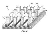
FIGS. 1-3 are perspective views illustrating embodiments of floatingbody cell structures body cells 104, the details of forming such are described in detail below. In some embodiments, the floatingbody cell structure 100 may be used to form a vertical multi-gate floating body cell device. Eachfloating body cell 104 in the array may include a volume ofsemiconductive material 102. The volume ofsemiconductor material 102 may includespillars 108 defined avoid 110, such as a u-shaped trench. An upper portion of thepillars 108 of each volume ofsemiconductive material 102 may be doped differently than remaining portions thereof to form asource region 112 and adrain region 114. By way of non-limiting example, thesource region 112 and thedrain region 114 may be doped with an n-type material, and the remaining portions of the volume ofsemiconductive material 102 may be doped with a p-type material. Thesource region 112 and drainregion 114 may, respectively, be electrically coupled to an access line, such ascommon source line 116 and a data/sense line, such asbit line 118, as will be described in further detail. By way of non-limiting example, acontact plug 119 may be disposed between at least one of thesource region 112 and thedrain region 114 and the associatedcommon source line 116 orbit line 118. Although thecontact plug 119 is shown inFIG. 1 as being disposed between thedrain regions 114 and thebit lines 118, thecontact plug 119 may additionally, or alternatively, be disposed between thesource regions 112 and the common source lines116.- As a non-limiting example, each of the floating
body cells 104 may be aligned with one another in an array that includes a plurality of rows extending in a first direction X and a plurality of columns extending in a second direction Y. The floatingbody cell structures FIGS. 1-3 each include two (2) rows and three (3) columns. However, as configured, the floatingbody cell structures body cells 104 aligned in the first direction X may be substantially perpendicular the columns of floatingbody cells 104 aligned in the second direction Y. - The floating
body cells 104 may be disposed on aback gate 123 that may include, for example, adielectric material 126, aconductive material 124 and anamorphous silicon material 128. For ease of description,conductive material 124 will hereinafter be referred to asback gate electrode 124 and thedielectric material 126 will hereinafter be referred to asback gate dielectric 126. The floatingbody cells 104 may each be electrically coupled to theback gate 123. Optionally, each of theback gate electrodes 124 may include ametal 127 and a dopedregion 125. Theback gate electrodes 124 may be formed from, for example, a titanium-rich titanium nitride material, such as metal mode titanium nitride (MMTiN), a tantalum nitride material or a tantalum silicide material. Theback gate dielectric 126 and themetal 127 form a metal-insulator-metal (MIM) structure that may function as a capacitor in the floatingbody cell structures metal 127 and the dielectric constant (k-value) of theback gate dielectric 126, and the thicknesses of theback gate dielectric 126 and themetal 127. Increasing capacitance in this manner may provide increased retention times in the floatingbody structures - The
back gate electrode 124 may overlie anamorphous silicon material 128 disposed on an electricallyinsulative material 130, which may be formed on, for example, a wafer (not shown). In some embodiments, theback gate 123 of each of the floatingbody cells 104 may be configured as a local back gate, having sidewalls continuous and aligned with those of the floatingbody cells 104, as shown inFIGS. 1 and 2 . A single floatingbody cell 104 may be disposed on theback gate 123 or, optionally, multiple floatingbody cells 104 may be disposed on theback gate 123. Theback gate 123 may be patterned as a plurality of local back gates that may be independently biased during operation of the cell or may be patterned as a global back gate. For example, as shown inFIG. 1 , theback gate 123 may be a local back gate that extends in the first direction X along at least one of the rows and the plurality of floatingbody cells 104 aligned in that row may be disposed thereon. In other embodiments, as shown inFIG. 2 , theback gate 123 may be a local back gate that extends in the second direction Y along at least one of the columns and the plurality of floatingbody cells 104 arranged in that column may be disposed thereon. As a non-limiting example, each of theback gates 123 may be aligned substantially parallel to an overlying one of the bit lines118. In additional embodiments, as shown inFIG. 3 , theback gate 123 of the floatingbody cell structure 100 may be a global back gate upon which the plurality of floatingbody cells 104, aligned in both the first direction X and the second direction Y, may be disposed. - A
conductive element 132 may be disposed within thevoid 110 of each floatingbody cells 104. For the ease of description, theconductive element 132 is hereinafter referred to as buriedgate electrode 132. Anotherdielectric material 134 may be disposed between the buriedgate electrode 132 and the semiconductive material exposed within the void110 in the floatingbody cell 104. For the ease of description, thedielectric material 134 is hereinafter referred to as buriedgate dielectric 134. The buried gate dielectric134 may, optionally, terminate below or at the respective interfaces between thechannel region 106 of each of the floatingbody cells 104 and thesource region 112 and thedrain region 114 in the upper portions of thepillars 108. Electromagnetic fields emanating from the buriedgate electrode 132 may establish a channel through the associated floatingbody cell 104, which enables a current to flow from thesource region 112 to thedrain region 114. - During use and operation of floating
body cell 104, the majority carrier is stored at a location within the floatingbody cells 104 isolated from each of the buriedgate electrode 132, thesource region 112 and thedrain region 114. As a result, charge retention and reliability may be enhanced compared to conventional floating body cell structures. As configured, a thickness of the volume ofsemiconductive material 102 may be varied to further distance the location of the stored charge from the buriedgate electrode 132, thesource region 112 and thedrain region 114, as described in greater detail herein. Moreover, as configured, the volume ofsemiconductive material 102 may be formed to have a larger storage volume in comparison to a floating body of conventional structures. This enables increased charge storage within the floatingbody cell 104 and, therefore, may minimize signal fluctuation due to lost charge. As a result, floatingbody cell 104 may provide an enhanced signal, longer retention and increased reliability in comparison to conventional structures. - In some embodiments, the floating
body cell structures body cell structures body cell structures - With reference to
FIGS. 4-14 , a method of forming floatingbody cell structures body cells 104, such as those shown inFIGS. 1-3 , will now be described, wherein like elements are designated by like numerals. Referring toFIG. 4 , asemiconductor structure 140 may be provided that includes asemiconductive material 142 overlying and contacting theback gate dielectric 126, theback gate dielectric 126 overlying and contacting theback gate contact 124, theback gate electrode 124 overlying and contacting theamorphous silicon material 128, and theamorphous silicon material 128 overlying and contacting the electricallyinsulative material 130. Thesemiconductor structure 140 may, optionally, include the dopedregion 125 and themetal 127, as shown in broken lines. In some embodiments, the electricallyinsulative material 130 may be formed over ahandle wafer 144. As used herein, the term “wafer” means any structure that includes a semiconductor type material including, for example, silicon, germanium, gallium arsenide, indium phosphide, and other III-V or II-VI type semiconductive materials. Wafers include, for example, not only conventional wafers but also other bulk semiconductor substrates such as, by way of non-limiting example, silicon-on-insulator (SOI) type substrates, silicon-on-sapphire (SOS) type substrates, and epitaxial layers of silicon supported by another material. Furthermore, when reference is made to a “wafer” in the following description, previous process steps may have been utilized to at least partially form elements or components of a circuit or device in or over a surface of the wafer. In some embodiments, the electricallyinsulative material 130 may be disposed over memory elements (not shown), such as a complementary metal oxide semiconductor structure (CMOS) device, formed in or on thehandle wafer 144. Theelectrically insulative material 130 may include, for example, a buried oxide (BOX) material. - The
semiconductor structure 140 may be formed, for example, by transferring theamorphous silicon material 128, theback gate contact 124, theback gate dielectric 126 and thesemiconductive material 142 to the electricallyinsulative material 130 overlying thehandle wafer 144 by a process described herein using a modification of so-called SMART-CUT® layer transfer technology. Such processes are described in detail in, for example, U.S. Pat. No. RE 39,484 to Bruel, U.S. Pat. No. 6,303,468 to Aspar et al., U.S. Pat. No. 6,335,258 to Aspar et al., U.S. Pat. No. 6,756,286 to Moriceau et al., U.S. Pat. No. 6,809,044 to Aspar et al., U.S. Pat. No. 6,946,365 to Aspar et al., and U.S. Patent Application Publication No. 2006/0099776 to Dupont. However, other processes suitable for manufacturing thesemiconductor substrate 140 may also be used. In conventional implementation of the SMART-CUT® layer transfer technology, donor wafers and acceptor wafers are bonded together using a high temperature anneal. The temperature used to bond the donor and acceptor wafers is from about 1000° C. to about 1300° C. However, due to the presence of theback gate contact 123, it may be advantageous to fabricate thesemiconductor structure 140 at decreased temperatures to prevent thermal damage to theback gate contact 123. Accordingly, as described herein, thesemiconductor structure 140 may be formed using substantially reduced temperatures in comparison to those required by conventional SMART-CUT® layer transfer technology. - Referring to
FIG. 5 , aworkpiece 146 may be formed by respectively depositing theback gate dielectric 126, theback gate electrode 124 and theamorphous silicon material 128 over thesemiconductive material 142, which may comprise a portion of, for example, a donor wafer. Optionally, theworkpiece 146 may include themetal 127 and the dopedregion 125. The dopedregion 125 may be formed using conventional methods, such as an ion implantation process or a high temperature diffusion process and may have a thickness between about 10 nm and about 50 nm. Themetal 127, if present, may comprise a titanium nitride material, such as metal mode titanium nitride (MMTiN), a titanium silicide material, a tantalum nitride material or a tungsten silicide material. Themetal 127 may be formed over and in contact with the dopedregion 125 using a CVD process, a PVD process, a sputtering process or a plating process and may have a thickness between about 10 nm to about 30 nm. Theback gate dielectric 126 may include, for example, an oxide material, a high k dielectric material or a nitride material and may be formed over and in contact with thesemiconductive material 142 or themetal 127, if present, using a CVD process or by decomposing tetraethyl orthosilicate (TEOS). As a non-limiting example, theback gate dielectric 126 may have a thickness of from about 20 Å to about 70 Å. Theback gate electrode 124 may include a conductive material, such as a metal material. The conductive material may be titanium nitride material, a titanium silicide material, a tungsten silicide material or a tantalum nitride material and may be formed over and in contact with theback gate dielectric 126 using a CVD process, a PVD process, a sputtering process or a plating process. By way of non-limiting example, theback gate electrode 124 may have a thickness of from about 100 Å to about 600 Å. Theamorphous silicon material 128 may be formed over and in contact with theback gate dielectric 126 using, for example, a PVD process or a CVD process. As a non-limiting example, theamorphous silicon material 128 may have a thickness of from about 100 Å to about 400 Å. - An atomic species may be implanted into the
semiconductive material 142 to form atransfer region 150. The atomic species may be hydrogen ions, ions of rare gases, also termed inert or noble gases, or ions of fluorine. The atomic species may be implanted into thesemiconductive material 142 to form an implantedzone 152, which is shown in thesemiconductive material 142 in broken lines. The atomic species may be implanted into thesemiconductive material 142 prior to formation of one or all of theback gate dielectric 126, theback gate electrode 124 and theamorphous silicon material 128 thereon or after formation of theback gate dielectric 126, theback gate electrode 124 and theamorphous silicon material 128 thereon. As known in the art, the depth at which the ions are implanted into thesemiconductive material 142 is at least partially a function of the energy with which the ions are implanted into thesemiconductive material 142. The implantedzone 152 may be formed at a desired depth in thesemiconductive material 142, which is dependent on parameters, such as implant dose and energy of the atomic species, as known in the art. A depth D of the implantedzone 152 within thesemiconductor structure 142 may correspond to a desired thickness and/or volume of the floatingbody cells 104 shown inFIGS. 1-3 . The volume of the floatingbodies 102 and the amount of charge that may be stored therein may be increased by increasing the depth D and, thus, the thickness of thesemiconductive material 142. Furthermore, by increasing the thickness of the floatingbody cells 104, the charge stored therein may be further isolated from conductive elements of the floatingbody cell structures gate electrode 132, thesource regions 112 and drain regions114). By isolating the stored charge from the conductive elements, charge loss may be decreased and, thus, the floatingbody cells 104 may provide increased retention and improved reliability. As a non-limiting example, the atomic species may be implanted into thesemiconductive material 142 with an energy selected to form the implantedzone 152 at a depth D of between about 100 nm and about 350 nm (about 1000 Å to about 3500 Å). - The implanted
zone 152 includes a layer of microbubbles or microcavities comprising the implanted ion species, and provides a weakened structure within thesemiconductive material 142. Thesemiconductive material 142 may then be thermally treated at a temperature above that at which implantation is effected to effect crystalline rearrangement in the wafer and coalescence of the microbubbles or microcavities. Optionally, the attachment surface (not shown) may be formed by exposing the major surface of theamorphous silicon material 128 of thesemiconductive material 142 to a reactive ion etching (RIE) plasma including an inert gas (e.g., argon, oxygen, or nitrogen) to form a plasma-activated material, or by exposing the surface to a dilute ammonia hydroxide or hydrogen fluoride solution. Forming an attachment surface on theamorphous silicon material 128 may increase the kinetics of a subsequent bonding act with theelectrically insulative material 130 overlying thehandle wafer 144, due to the increased mobility of the ionic species (e.g., hydrogen). - As shown in
FIG. 6 , theworkpiece 146 may be superposed on theelectrically insulative material 130 overlying thehandle wafer 144 so that the electricallyinsulative material 130 is in contact with theamorphous silicon material 128 of theworkpiece 146. Theamorphous silicon material 128 of theworkpiece 146 may be bonded to the electricallyinsulative material 130. By way of non-limiting example, theamorphous silicon material 126 and theelectrically insulative material 130 may also be bonded without heat at ambient temperature (from about 20° C. to about 25° C.). Pressure may also be applied to at least one of theworkpiece 146 and thehandle wafer 144 to bond theamorphous silicon material 128 to the electricallyinsulative material 130. As another non-limiting example, theamorphous silicon material 126 may be bonded to theinsulator material 104 by heating thesemiconductor structure 140 to a temperature of less than about 600° C., such as from about 300° C. to about 400° C. If the electricallyinsulative material 130 is formed from silicon dioxide, silicon-oxide bonds may form between theamorphous silicon material 128 and theinsulator material 130. Because theback gate electrode 124 may be formed of a metal or other heat sensitive material, the temperature to which thesemiconductor structure 140 is exposed may be less than the melting point of theback gate contact 124. - To form the
semiconductor structure 140 shown inFIG. 4 , thetransfer region 150 may be removed from thesemiconductive material 142, along the implanted zone shown inFIG. 6 . Thetransfer region 150 may be removed by techniques known in the art, such as by applying a shear force to the implantedzone 152 or by applying heat or a jet gas stream at the implantedzone 152. The atomic species in the implantedzone 152 produce a weakened region in thesemiconductive material 142 of theworkpiece 146, which is susceptible to cleavage. - The
back gate dielectric 126, theback gate contact 124, and theamorphous silicon material 128 and a portion of thesemiconductive material 142 below the implantedzone 152 may remain bonded to the electricallyinsulative material 130 to form thesemiconductor structure 140 shown inFIG. 4 . After separation of thesemiconductive material 142, an exposedsurface 154 thereof may be undesirably rough. To remedy this deficiency, the exposedsurface 154 of thesemiconductive material 142 may be smoothed to a desired degree in order to facilitate further processing as described, according to techniques known in the art, for example, one or more of grinding, wet etching, and CMP. FIG. 7 shows thesemiconductor structure 140 ofFIG. 4 after amask material 156 has been deposited on thesemiconductive material 142 and patterned to form apertures through which surfaces154 of thesemiconductive material 142 are exposed. Themask material 156 may include, for example, a photoresist material, an oxide material, transparent carbon or amorphous carbon. Methods of forming and patterning themask material 156 are known in the art and, therefore, are not described in detail herein. For the sake of simplicity, thehandle wafer 144 underlying the electricallyinsulative material 130 has been omitted from the remaining figures.- As shown in
FIG. 8A , portions of thesemiconductive material 142 exposed through the apertures in themask material 156 may be removed to formtrenches 158 between remaining portions of thesemiconductive material 142. The remaining portions of themask material 156 may then be removed. By way of non-limiting example, thetrenches 158 may be formed extending through thesemiconductive material 142 in the second direction Y. A reactive ion etching (RIE) process to selectively remove thesemiconductive material 142 with respect to themask material 156 and theback gate dielectric 126. In some embodiments, as shown inFIG. 8B , after removing the portions of thesemiconductive material 142, portions of each of theback gate dielectric 126, theback gate electrode 124 and theamorphous silicon material 128 may be removed in situ through thesame mask material 156, to form an individual orsingle back gate 123 such as that shown in the floatingbody cell structure 101 ofFIG. 2 .FIG. 2 shows continuous124,126,128 portions of theback gate dielectric 126, theback gate electrode 124 and theamorphous silicon material 128 may be removed using, for example, an anisotropic reactive ion (i.e., plasma) etching process, to expose the underlying electricallyinsulative material 130. For example, if theback gate dielectric 126 is formed from silicon dioxide, a reactive ion etching (RIE) process using a nitrogen trifluoride (CF3)-based gas, a chlorine (Cl)-based gas or a bromide (Br)-based gas may be performed to selectively remove theback gate 123 from the silicon dioxide with respect to themask material 156. If theback gate electrode 124 is titanium nitride, an anisotropic etching process using a tetrafluoromethane (CF4) gas, a mixture of a bromine-containing gas and a fluorine-containing gas or a mixture of a fluorine-containing gas and a chlorine-containing gas to remove the titanium nitride with respect to themask material 156. If theamorphous silicon material 128 is amorphous polysilicon, an anisotropic etching process using a mixture of a fluorine-containing gas and a chlorine-containing gas may be used to remove the amorphous silicon material with respect to themask material 156. In other embodiments, thetrenches 158 may be formed using a conventional pitch-doubling process, by techniques known in the art. FIG. 9 shows thesemiconductor structure 140 after depositing afill material 160 in thetrenches 158. WhileFIG. 9 showstrenches 158 extending through theback gate dielectric 126, theback gate contact 124, and theamorphous silicon material 128, thechannels 128 to be filled may be as shown inFIG. 8A . By way of non-limiting example, thefill material 160 may include a dielectric material such as an oxide material or a nitride material, and may be deposited using a chemical vapor deposition process or a spin-on dielectric process.FIGS. 10-13 are cross-sectional views of thesemiconductor structure 140 shown inFIG. 9 , taken along section line9-9, after asacrificial mask material 162 has been deposited thereover and a plurality ofopenings 164 have been formed. Thesacrificial mask material 162 may be formed over thesemiconductive material 142 and the fill material (not shown) and the plurality ofopenings 164 may be formed by removing portions of thesacrificial mask material 162 and thesemiconductive material 142. Each of the plurality ofopenings 164 may be formed extending in the second direction Y. As a non-limiting example, thesacrificial mask material 162 may be formed from an amorphous silicon material or a dielectric material using a CVD process. By way of non-limiting example, theopenings 164 may be performed by providing a photoresist material (not shown) over thesacrificial mask material 162 and removing portions of the photoresist material overlying regions ofsacrificial mask material 162 and thesemiconductive material 142 that are to be removed. An anisotropic etching process (e.g., a dry reactive ion or plasma etching process) may then be used to etch the regions of thesacrificial mask material 162 and thesemiconductive material 142 exposed through the photoresist material to formopenings 164 that expose regions of thesacrificial mask material 162. For example, if thesacrificial mask material 162 and thesemiconductive material 142 are formed from polysilicon, a reactive ion etching process using a fluorine (Fl)-based gas may be performed to selectively remove the amorphous silicon material, forming theopenings 164 between portions of thesemiconductive material 142. As a non-limiting example, theopenings 164 may be formed to have a dimension D1 of 0.5 F and the remaining portions of thesemiconductive material 142 may have a dimension D2 of 1.5 F. Additionally, theback gates 123, as shown inFIG. 1 , may be formed by removing a portion of each of theback gate dielectric 126, theback gate electrode 124 and theamorphous silicon material 130 after removing thesemiconductive material 142 such that theopenings 164 extend through each of these materials leaving theback gate 123 intact. After forming theopenings 164, the remaining photoresist material may be removed using a conventional ashing process. Theopenings 164 may also be formed using a conventional pitch-doubling process, by techniques known in the art.- As shown in
FIG. 11 , anotherfill material 166 such as an oxide material or a nitride material may be deposited in theopenings 164. By way of non-limiting example, thefill material 166 may be deposited using a CVD process, a PECVD process or spin-on dielectric process. Thus, thesemiconductive material 142 is completely physically isolated from the surrounding environment. - As shown in
FIG. 12 , a portion of each of thesacrificial material 162 and thesemiconductive material 142 may be removed to form thevoids 110 in thesemiconductive material 142. If thesemiconductive material 142 is formed from a crystalline silicon material, a plasma including a mixture of sulfur hexafluoride (SF6) gas, oxygen gas and helium (He) gas, or a mixture of sulfur hexafluoride gas and trifluoromethane (CHF3) gas, may be introduced to thesemiconductor structure 140 to form thevoids 110.FIG. 11 depicts thevoids 110 as having a u-shaped profile; however, voids having various other profiles may also be formed, as will be recognized by one of ordinary skill in the art. FIG. 13 shows thesemiconductor structure 140 after the buriedgate electrodes 132 have been formed in each of thevoids 110. As a non-limiting example, a CMP process may be used to remove portions of thefill material 166 and thesacrificial material 162 so that anupper surface 168 of thesemiconductor structure 140 is substantially planar. The buriedgate electrodes 132 may be formed from a conductive material such as, tungsten, titanium nitride or tantalum nitride, and may be deposited using a conventional CVD process, PVD process or ALD process. By way of non-limiting example, the conductive material may be formed over thesemiconductor structure 140 and removed after deposition using a conventional CMP process, RIE process or wet etching process to form the buriedgate electrodes 132. The buried gate dielectric134 may be deposited over sidewalls of thesemiconductive material 142 exposed in each of thevoids 110 before forming the buriedgate electrodes 132.FIG. 14 shows thesemiconductor structure 140 after forming the buriedgate electrodes 132 in thevoids 110 and anotherfill material 163 thereover. As shown inFIG. 14 ,source regions 112 anddrain regions 114 may be formed in exposed regions of thepillars 108 of the volume ofsemiconductive material 102. Thesource regions 112 anddrain regions 114 may include a silicon material that is doped with an n-type dopant, such as phosphorous or arsenic, (i.e., n-type silicon material). Exposed portions of thesemiconductive material 142 may be doped using conventional methods, such as an ion implantation process or plasma ion process or a high temperature diffusion process. Thesource regions 112 and thedrain regions 114 may be spaced apart from theback gate electrode 124 by thesemiconductive material 142. As another example, a thin film of a n-type material (not shown) may be deposited over surfaces of thesemiconductor structure 140 and a thermal anneal may be performed during which n-type dopants migrate into thesemiconductive material 142 to form n-type silicon for thesource regions 112 anddrain regions 114. Thesource regions 112 anddrain regions 114 may, optionally, be formed before forming the buriedgate electrodes 132.- Referring back to
FIGS. 1-3 , after forming thesource regions 112 and thedrain regions 114, thecommon source lines 116 may be formed over thesource regions 112 aligned in each of the rows and thebit lines 118 may be formed over thedrain regions 114 aligned in each of the columns. In some embodiments, thecommon source lines 116 and thebit lines 118 may be formed by depositing a conductive reactive material over thesemiconductor structure common source lines 116 may be formed in the direction X, each of thecommon sources lines 116 disposed above and substantially parallel to one of the buriedgate electrodes 132. The bit lines118 may be formed extending in the direction Y. Optionally, thecontact plug 119 may be formed on at least one of thedrain regions 114 and thesource regions 112 to elevate that contact before forming the associatedcommon source line 116 orbit line 118. For example, thecontact plug 119 may be formed by depositing and patterning a doped amorphous silicon material. Optionally, thecontact plug 119 may be replaced by a metal material, such as titanium nitride/tungsten, or the contact plug may be filled with the conductive reactive material during formation of the conductive lines. FIG. 15 is a perspective view illustrating another embodiment of a floatingbody cell structure 200 that includes a plurality of floatingbody cells 104, the details of forming such will be described in detail. For the purposes of illustrating the floatingbody cells 104, a portion of thegate 170 has been removed, as shown in broken lines. In some embodiments, the floatingbody cell structure 200 may be used to form a vertical multi-gate floating body cell device. Each floatingbody cell 104 in the floatingbody cell structure 200 may include a floatingbody cell 104 formed from a volume of semiconductive material that includes achannel region 106 extending betweenpillars 108, which are separated by avoid 110, such as, a u-shaped trench, as described with respect toFIGS. 1-3 . Thesource regions 112 and thedrain regions 114 may be formed in the upper regions of thepillars 108 and may, respectively, be electrically coupled to an access line, such ascommon source line 116 and a data/sense line, such asbit line 118. By way of non-limiting example, thecommon source line 116 and thebit line 118 may, respectively, be formed directly on thesource regions 112 and thedrain regions 114, as shown inFIG. 18 . Additionally, acontact plug 119 may be disposed between thesource regions 112 and the associatedcommon source line 116 to elevate the contact or between thedrain regions 114 and the associatedbit line 118.- The floating
body cells 104 may be arranged as described with respect toFIGS. 1-3 , wherein the floatingbody cells 104 are aligned in a plurality of rows in the first direction X and the plurality of columns in the second direction Y substantially perpendicular to the first direction X.FIG. 4 shows theback gate 123 as a local back gate disposed under rows of floatingbody cells 104 and extending in a direction parallel to floatingbody cells 104. The sidewalls of theback gate 123 are shown as being continuous and aligned with those of the floatingbody cells 104. In other embodiments, theback gate 123 may be configured as described with respect toFIGS. 2 and 3 . - At least one
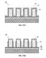
conductive element 170 may be disposed on opposite vertical surfaces (i.e., sidewalls) of each of the floatingbody cells 104. For the ease of description, theconductive element 170 is hereinafter referred to asgate 170. Anotherdielectric material 172 may be disposed between thegate 170 and the sidewalls of the floatingbody cells 104. For the ease of description, thedielectric material 172 is hereinafter referred to asgate dielectric 172. Each of the floatingbody cells 104 of the floatingbody cell structure 200 may be electrically coupled to theback gate 123 and thegates 170 disposed on two sidewalls of the floatingbody cells 104 so that the floatingbody cell 104 includes three gates, or may be electrically coupled to theback gate 123 and thegate 170 disposed on a single sidewall of the floatingbody cells 104 so that the floatingbody cell 104 includes two gates. Electromagnetic fields emanating from thegates 170 may establish a channel through the associated floatingbody 104, which enables a current to flow from thesource region 112 to thedrain region 114. FIGS. 16-20 illustrate embodiments of a method of forming the floatingbody cell structure 200 shown inFIG. 15 . Referring toFIG. 16 , asemiconductor structure 240 that includes an array of floatingbody cells 104, each including a volume ofsemiconductive material 102 disposed on theback gate 123 may be formed using methods such as those described with respect toFIGS. 4-12 . Theback gate 123 may include backgate dielectric 126, backgate electrode 124 andamorphous silicon material 128 and may be disposed on an electricallyinsulative material 130 overlying a wafer (not shown). As previously described, other logic elements (not shown), such as a complementary metal oxide semiconductor structure (CMOS) device, may be formed in or on the wafer. Although thetrenches 158 are illustrated as terminating within the electricallyinsulative material 130, thetrenches 158 may, optionally, be formed to terminate on theback gate dielectric 126, such as those described with respect toFIG. 8A .- FIGS.17A1-17B2 are cross-sectional views of the
semiconductor structure 140 shown inFIG. 16 , taken along section line16-16. After forming thetrenches 158, thegates 170 may be formed on sidewalls of the floatingbody cells 104, as described with respect to FIGS.17A1-17B2. As shown in FIG.17A1, agate dielectric material 172 and aconductive material 174 may be formed oversemiconductor structure 240. By way of non-limiting example, thegate dielectric material 172 may be an oxide material, a nitride material or a high k dielectric material formed using, for example, a chemical vapor deposition process or a thermal oxidation process. For example, if thegate dielectric material 172 is silicon dioxide, thesemiconductor structure 240 may be exposed to an oxygen gas at a temperature of from about 900° C. to about 1175° C. to form the silicon dioxide on sidewalls of the floatingbody cells 104. Theconductive material 174 may then be formed over thegate dielectric material 172. As a non-limiting example, theconductive material 174 may be formed from titanium nitride, tantalum nitride or tungsten and may be deposited using a chemical vapor deposition process. Referring to FIG.17A2, an anisotropic dry etching process or a wet etching process may be performed to remove portions of theconductive material 174 and thegate dielectric material 172 to form thegates 170. - In other embodiments, the
gates 170 may be formed on the sidewalls of the floatingbody cells 104 as shown with respect to FIGS.17B1 and17B2. Referring to FIG.17B1, after forming thegate dielectric material 172 over thesemiconductive material 142, the remaining portions of thetrenches 158 between regions of thesemiconductive material 142 may be filled with theconductive material 174 and theconductive material 174 may be recessed back to a desired thickness. By way of non-limiting example, theconductive material 174 may be formed from titanium nitride, tantalum nitride or tungsten and may be deposited using a chemical vapor deposition process.Spacers 176 including a dielectric material may be formed on sidewalls of thegate dielectric material 172 above theconductive material 174 using a conventional spacer etching process. Referring to FIG.17B2, an anisotropic etching process may be performed to remove a portion of theconductive material 174 to form thegates 170. After forming thegates 170, thespacers 176 may be removed using, for example, a conventional selective etching process. FIGS. 18A and 18B are top down views of thesemiconductor structure 240 shown in FIGS.17A2 and17B2 illustrating the configuration of thegates 170. Thegates 170 may be formed to electrically connect pluralities of the floatingbody cells 104 with one another. As a non-limiting example, thegates 170 may extend along the columns of floatingbody cells 104 in direction Y. As shown inFIG. 18A , each of thegates 170 may substantially circumscribe the plurality of floatingbody cells 104 in a single one of the columns, vertical surfaces (i.e., sidewalls) of each of the floatingbody cells 104 being contacted by thegate 170. Referring toFIG. 18B , another embodiment is shown wherein thegates 170 are configured in a comb-like structure extending along at least one of the rows in a direction X and terminating at or near an end thereof, each of thegates 170 being disposed on opposite sidewalls of the floatingbody cells 104 in the row.Contacts 178 may be electrically coupled to each of thegates 170, for example, at a terminal portion thereof, so that thegates 170 are independently connected. Accordingly, as shown inFIGS. 18A and 18B , thegates 170 may be configured to form single-gate, dual-gate and triple-gate floatingbody cells 104.- As shown in
FIG. 19 , after forming thegates 170,source regions 112 anddrain regions 114 may be formed in the upper portion of thepillars 108 of floatingbody cells 104 by exposing thesemiconductor structure 240 to an n-type dopant or a p-type dopant, as described with respect toFIG. 14 . Thecommon source lines 116 may then be formed over thesource regions 112 of the floatingbody cells 104 and thebit lines 118 may be formed over thedrain regions 114 of the floatingbody cells 104 to form thesemiconductor structure 240 shown inFIG. 18 . Thecommon source lines 116 andbit lines 118 may be formed by depositing a conductive material and pattering the conductive material to form conductive lines extending in the first direction X, substantially perpendicular to thegates 170. Since thecommon source lines 116 andbit lines 118 are parallel to another, thecommon source lines 116 andbit lines 118 may be formed using a conventional damascene process. For example, a sacrificial dielectric material (not shown) may be deposited over thesemiconductor structure 240 and a pattern of apertures may be formed therein in locations at which thecommon source lines 116 andbit lines 118 are to be formed using a conventional lithographic process. A conductive material may be deposited over thesemiconductor structure 240 to fill the apertures and a chemical mechanical polishing process may be used to remove a portion of the conductive material overlying the dielectric material to form thecommon source lines 116 and bit lines118. Optionally, a doped material (not shown) may be formed on at least one of thesource regions 112 anddrain regions 114 before forming the associatedcommon source line 116 orbit line 118. FIGS. 20-22 are electrical circuit diagrams, each of which illustrates a floating body cell structure that includes a plurality of floating body cells, such as those described with respect toFIGS. 1-3 and15. As shown inFIG. 20 , the floatingbody cell structure 300 may include a plurality of floatingbody cells 104, each of which is electrically coupled to agate 132, abit line 118 and aglobal back gate 123, such as theback gate 123 shown inFIG. 2 . Theglobal back gate 123 and thegate 132 may each be operably coupled to a bias voltage enabling the floatingbody cells 104 associated with theglobal back gate 123 to be simultaneously biased.FIG. 21 illustrates a floatingbody cell structure 400 including a plurality of floatingbody cells 104, each of which is electrically coupled to agate 132, abit line 118 and alocal back gate 123. Thelocal back gates 123 may have a comb-like configuration, such as that shown inFIG. 18B , to provide two distinct addresses for each of thelocal back gates 123.FIG. 22 illustrates a floatingbody cell structure 500 including a plurality of floatingbody cells 104, each of which is electrically coupled to agate 132, abit line 118 and alocal back gate 123, such as theback gates 123 shown inFIGS. 2 and 15 . Each of thelocal back gates 123 may be operably coupled to a bias voltage that may be used to individually bias each of theback gates 123.- It should be noted that, during the various stages of fabrication, the floating
body cell structures FIGS. 1 through 3 , may be integrated or vertically stacked with other semiconductor structures having a similar structure or with a memory element or device, such as a CMOS device. For example, the CMOS device may be formed over or beneath one of the floatingbody cell structures body cell structures FIGS. 4-6 . FIG. 23 illustrates a simplified block diagram of anelectronic system 2300 implemented according to one or more embodiments described herein. Theelectronic system 2300 includes at least oneinput device 2302, at least oneoutput device 2304, a memory access device, such as one ormore processors 2306, such as a system-on-chip (SOC), a central processing unit (CPU), processors and the like that may, and one ormore memory devices 2308. Thememory devices 2308 include at least one embodiment of the devices or methods described herein. Theelectronic system 2300 may be part of a number of computing, processing, and consumer products. As non-limiting examples, some of these products may include personal computers, handheld devices, cameras, phones, wireless devices, displays, chip sets, set top boxes, games, and vehicles.- In some embodiments, the present invention includes floating body cell structures, devices including such structures and method for forming such structures. The floating body cell structures may include a back gate, at least one floating body and another gate associated with the at least one floating body. The at least one floating body may include a semiconductive material and may extend from the back gate to a source region and a drain region. The source region and the drain region may be spaced apart from the back gate by the at least one floating body. The at least one floating body may include a void in the semiconductive material, each of the source region and the drain region disposed opposite the back gate. The another gate may be disposed within the void in the at least one floating body to form a double-gate floating body cell structure or may be disposed on at least one surface of the at least one floating body to form a triple-gate floating body cell structure. A gate dielectric may be disposed between the back gate and the at least one floating body and an amorphous silicon material underlying the back gate and disposed over a wafer. The back gate may be a local back gate comprising sidewalls continuous and aligned with sidewalls of the at least one floating body or a global back gate in which a plurality of floating body cells are disposed in an array. The floating body cell structure may further include a bit line electrically coupled to the back gate and operably coupled to a bias voltage for independently biasing the back gate. The floating body cell structure may further include a common source line electrically coupling the source region of the at least one floating body cell to a source region of at least another floating body and a bit line electrically coupling the drain region of the at least one floating body cell to a drain region of the at least another floating body.
- In additional embodiments, the present invention includes a floating body cell device that includes a plurality of floating bodies, each comprising a semiconductive material and extending from a back gate to a source region and a drain region and another gate associated with the plurality of floating bodies and operably coupled to a voltage source and a common source line electrically coupling the source regions of the plurality of floating bodies and a bit line electrically coupling the drain regions of the plurality of floating bodies. The device may be integrated in at least one of a dynamic random access memory, a zero capacitor random access memory, a central processing unit, a system-on-a-chip and embedded dynamic random access memory integrated therewith. The plurality of floating bodies may be aligned in a first direction to form a plurality of rows and a second direction substantially perpendicular to the first direction to fat m a plurality of columns.
- In yet further embodiments, a floating body cell device includes a plurality of floating bodies aligned in a first direction to form a plurality of rows and aligned in a second direction substantially perpendicular to the first direction to form a plurality of columns, at least one back gate associated with the plurality of the floating bodies and at least another gate associated with the plurality of floating bodies and operably coupled to a voltage source. Each of the floating bodies of the plurality of floating bodies may include a volume of semiconductive material having pillars extending from a base portion thereof and separated by a u-shaped trench, an upper portion of each of the pillars comprising a doped region. The at least one back gate may include a conductive material disposed over an amorphous silicon material on an electrically insulative material. The at least another gate may include a conductive material disposed on each of the plurality of floating bodies that may extend, for example, in the first direction, electrically coupling the plurality of floating bodies in at least one of the plurality of rows. The at least another gate may include a conductive material disposed within the u-shaped trench and, for example, may extend in the second direction, electrically coupling the plurality of floating bodies in at least one of the plurality of columns. The at least one back gate may be configured to be biased independent of the another gate. The floating body cell structure may be disposed over and integrated with a memory device, such as a CMOS device, or may be vertically stacked in a number of tiers to increase density.
- In yet further embodiments, the present invention includes methods of forming a floating body cell device that include forming a base comprising a semiconductive material, a dielectric material, a gate material, and an amorphous silicon material overlying a wafer, removing a portion of the semiconductive material to form a plurality of floating bodies protruding from a surface of the base, removing another portion of the semiconductive material to form a void in each of the plurality of floating bodies, exposing the plurality of floating bodies to at least one dopant to form a source region and a drain region in upper regions of each of the plurality of floating bodies and forming a gate associated with at least one of the plurality of floating bodies. The base may be formed by forming a donor wafer comprising a dielectric material, a gate material and an amorphous silicon material overlying a crystalline silicon wafer, implanting ions a predetermined depth into the crystalline silicon wafer, attaching the amorphous silicon material of the donor wafer to an electrically insulative material overlying a handle wafer; and separating a portion of the donor wafer to leave a portion of the crystalline silicon wafer so that the dielectric material, the gate material, and the amorphous silicon material overlying a surface of the electrically insulative material of the handle wafer.
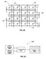
- In yet further embodiments, the present invention includes a system that includes at least one memory device and at least one floating body cell device operably coupled to the at least one memory device. The at least one floating body cell device may include an array of floating bodies, each of which includes a volume of semiconductive material having pillars extending from a base portion thereof and separated by a u-shaped trench, an upper portion of each of the pillars comprising a doped region, at least one back gate associated with the array of the floating bodies and at least another gate associated with the plurality of floating bodies and operably coupled to a voltage source. The system may include at least one of a central processing unit and a system-on-a-chip. The at least one memory device may include at least one of a dynamic random access memory, a zero capacitor random access memory, and an embedded dynamic random access memory. The at least one memory device and the at least one floating body cell device may be superposed with one another within the system.
- While the invention is susceptible to various modifications and alternative forms, specific embodiments have been shown by way of example in the drawings and have been described in detail herein. However, the invention is not intended to be limited to the particular forms disclosed. Rather, the invention is to cover all modifications, equivalents, and alternatives falling within the scope of the invention as defined by the following appended claims and their legal equivalents.
Claims (30)
Priority Applications (16)
| Application Number | Priority Date | Filing Date | Title |
|---|---|---|---|
| US12/715,743US9646869B2 (en) | 2010-03-02 | 2010-03-02 | Semiconductor devices including a diode structure over a conductive strap and methods of forming such semiconductor devices |
| US12/715,843US8513722B2 (en) | 2010-03-02 | 2010-03-02 | Floating body cell structures, devices including same, and methods for forming same |
| US12/715,704US9608119B2 (en) | 2010-03-02 | 2010-03-02 | Semiconductor-metal-on-insulator structures, methods of forming such structures, and semiconductor devices including such structures |
| PCT/US2011/024387WO2011109149A2 (en) | 2010-03-02 | 2011-02-10 | Floating body cell structures, devices including same, and methods for forming same |
| CN201180011589.XACN102822972B (en) | 2010-03-02 | 2011-02-10 | Floating body cell structures, devices incorporating same and methods for forming same |
| JP2012556084AJP2013521651A (en) | 2010-03-02 | 2011-02-10 | Floating body cell, device including floating body cell, and method for forming floating body cell. |
| SG2012062246ASG183450A1 (en) | 2010-03-02 | 2011-02-10 | Floating body cell structures, devices including same, and methods for forming same |
| EP11751053.7AEP2543068A4 (en) | 2010-03-02 | 2011-02-10 | FLOATING BODY CELL STRUCTURES, DEVICES COMPRISING SAME, AND METHODS OF FORMING THE SAME |
| KR1020127025450AKR101471734B1 (en) | 2010-03-02 | 2011-02-10 | Floating body cell structures, devices including same, and methods for forming same |
| TW100106776ATWI503874B (en) | 2010-03-02 | 2011-03-01 | Floating body unit structure, apparatus including the same, and method for forming the same |
| US13/609,997US8530295B2 (en) | 2010-03-02 | 2012-09-11 | Floating body cell structures, devices including same, and methods for forming same |
| US13/952,742US8841715B2 (en) | 2010-03-02 | 2013-07-29 | Floating body cell structures, devices including same, and methods for forming same |
| US13/953,450US8859359B2 (en) | 2010-03-02 | 2013-07-29 | Floating body cell structures, devices including same, and methods for forming same |
| US13/965,463US8980699B2 (en) | 2010-03-02 | 2013-08-13 | Thyristor-based memory cells, devices and systems including the same and methods for forming the same |
| US14/642,866US9343462B2 (en) | 2010-03-02 | 2015-03-10 | Thyristor-based memory cells, devices and systems including the same and methods for forming the same |
| US15/464,060US10325926B2 (en) | 2010-03-02 | 2017-03-20 | Semiconductor-metal-on-insulator structures, methods of forming such structures, and semiconductor devices including such structures |
Applications Claiming Priority (1)
| Application Number | Priority Date | Filing Date | Title |
|---|---|---|---|
| US12/715,843US8513722B2 (en) | 2010-03-02 | 2010-03-02 | Floating body cell structures, devices including same, and methods for forming same |
Related Child Applications (2)
| Application Number | Title | Priority Date | Filing Date |
|---|---|---|---|
| US13/609,997DivisionUS8530295B2 (en) | 2010-03-02 | 2012-09-11 | Floating body cell structures, devices including same, and methods for forming same |
| US13/952,742ContinuationUS8841715B2 (en) | 2010-03-02 | 2013-07-29 | Floating body cell structures, devices including same, and methods for forming same |
Publications (2)
| Publication Number | Publication Date |
|---|---|
| US20110215408A1true US20110215408A1 (en) | 2011-09-08 |
| US8513722B2 US8513722B2 (en) | 2013-08-20 |
Family
ID=44530577
Family Applications (4)
| Application Number | Title | Priority Date | Filing Date |
|---|---|---|---|
| US12/715,843Active2030-09-25US8513722B2 (en) | 2010-03-02 | 2010-03-02 | Floating body cell structures, devices including same, and methods for forming same |
| US13/609,997ActiveUS8530295B2 (en) | 2010-03-02 | 2012-09-11 | Floating body cell structures, devices including same, and methods for forming same |
| US13/952,742ActiveUS8841715B2 (en) | 2010-03-02 | 2013-07-29 | Floating body cell structures, devices including same, and methods for forming same |
| US13/953,450ActiveUS8859359B2 (en) | 2010-03-02 | 2013-07-29 | Floating body cell structures, devices including same, and methods for forming same |
Family Applications After (3)
| Application Number | Title | Priority Date | Filing Date |
|---|---|---|---|
| US13/609,997ActiveUS8530295B2 (en) | 2010-03-02 | 2012-09-11 | Floating body cell structures, devices including same, and methods for forming same |
| US13/952,742ActiveUS8841715B2 (en) | 2010-03-02 | 2013-07-29 | Floating body cell structures, devices including same, and methods for forming same |
| US13/953,450ActiveUS8859359B2 (en) | 2010-03-02 | 2013-07-29 | Floating body cell structures, devices including same, and methods for forming same |
Country Status (8)
| Country | Link |
|---|---|
| US (4) | US8513722B2 (en) |
| EP (1) | EP2543068A4 (en) |
| JP (1) | JP2013521651A (en) |
| KR (1) | KR101471734B1 (en) |
| CN (1) | CN102822972B (en) |
| SG (1) | SG183450A1 (en) |
| TW (1) | TWI503874B (en) |
| WO (1) | WO2011109149A2 (en) |
Cited By (27)
| Publication number | Priority date | Publication date | Assignee | Title |
|---|---|---|---|---|
| US20110215436A1 (en)* | 2010-03-02 | 2011-09-08 | Micron Technology, Inc. | Semiconductor devices including a diode structure over a conductive strap and methods of forming such semiconductor devices |
| US20110298040A1 (en)* | 2010-06-03 | 2011-12-08 | Hynix Semiconductor Inc. | Semiconductor device and method of manufacturing the same |
| US20120214285A1 (en)* | 2011-02-22 | 2012-08-23 | Jaydip Guha | Methods Of Forming A Vertical Transistor And At Least A Conductive Line Electrically Coupled Therewith, Methods Of Forming Memory Cells, And Methods Of Forming Arrays Of Memory Cells |
| US8569831B2 (en) | 2011-05-27 | 2013-10-29 | Micron Technology, Inc. | Integrated circuit arrays and semiconductor constructions |
| US8809145B2 (en) | 2010-03-02 | 2014-08-19 | Micron Technology, Inc. | Semiconductor cells, arrays, devices and systems having a buried conductive line and methods for forming the same |
| US8841715B2 (en) | 2010-03-02 | 2014-09-23 | Micron Technology, Inc. | Floating body cell structures, devices including same, and methods for forming same |
| US20140301126A1 (en)* | 2011-02-16 | 2014-10-09 | Micron Technology, Inc. | Memory Arrays and Methods of Forming Electrical Contacts |
| US8980699B2 (en) | 2010-03-02 | 2015-03-17 | Micron Technology, Inc. | Thyristor-based memory cells, devices and systems including the same and methods for forming the same |
| US9006060B2 (en) | 2012-08-21 | 2015-04-14 | Micron Technology, Inc. | N-type field effect transistors, arrays comprising N-type vertically-oriented transistors, methods of forming an N-type field effect transistor, and methods of forming an array comprising vertically-oriented N-type transistors |
| US9036391B2 (en) | 2012-03-06 | 2015-05-19 | Micron Technology, Inc. | Arrays of vertically-oriented transistors, memory arrays including vertically-oriented transistors, and memory cells |
| US9093367B2 (en) | 2010-11-03 | 2015-07-28 | Micron Technology, Inc. | Methods of forming doped regions in semiconductor substrates |
| US9111853B2 (en) | 2013-03-15 | 2015-08-18 | Micron Technology, Inc. | Methods of forming doped elements of semiconductor device structures |
| US9129983B2 (en) | 2011-02-11 | 2015-09-08 | Micron Technology, Inc. | Memory cells, memory arrays, methods of forming memory cells, and methods of forming a shared doped semiconductor region of a vertically oriented thyristor and a vertically oriented access transistor |
| US9129896B2 (en) | 2012-08-21 | 2015-09-08 | Micron Technology, Inc. | Arrays comprising vertically-oriented transistors, integrated circuitry comprising a conductive line buried in silicon-comprising semiconductor material, methods of forming a plurality of conductive lines buried in silicon-comprising semiconductor material, and methods of forming an array comprising vertically-oriented transistors |
| US9269795B2 (en) | 2011-07-26 | 2016-02-23 | Micron Technology, Inc. | Circuit structures, memory circuitry, and methods |
| US9337201B2 (en) | 2010-11-01 | 2016-05-10 | Micron Technology, Inc. | Memory cells, arrays of memory cells, and methods of forming memory cells |
| US9361966B2 (en) | 2011-03-08 | 2016-06-07 | Micron Technology, Inc. | Thyristors |
| US9443763B2 (en) | 2013-09-12 | 2016-09-13 | Micron Technology, Inc. | Methods for forming interconnections between top electrodes in memory cells by a two-step chemical-mechanical polishing (CMP) process |
| US9478550B2 (en) | 2012-08-27 | 2016-10-25 | Micron Technology, Inc. | Arrays of vertically-oriented transistors, and memory arrays including vertically-oriented transistors |
| US9608119B2 (en) | 2010-03-02 | 2017-03-28 | Micron Technology, Inc. | Semiconductor-metal-on-insulator structures, methods of forming such structures, and semiconductor devices including such structures |
| US20180006169A1 (en)* | 2016-07-01 | 2018-01-04 | Semiconductor Manufacturing International (Shanghai) Corporation | Method for fabricating nanopillar solar cell using graphene |
| CN108511511A (en)* | 2017-02-28 | 2018-09-07 | 东芝存储器株式会社 | Semiconductor device and manufacturing method thereof |
| US10361218B2 (en)* | 2017-02-28 | 2019-07-23 | Toshiba Memory Corporation | Semiconductor device and method for manufacturing same |
| US10373956B2 (en) | 2011-03-01 | 2019-08-06 | Micron Technology, Inc. | Gated bipolar junction transistors, memory arrays, and methods of forming gated bipolar junction transistors |
| CN113972275A (en)* | 2020-07-23 | 2022-01-25 | 美光科技公司 | Apparatus including vertical transistors having gate electrodes at least partially recessed within channel regions, and related methods and systems |
| US20220302212A1 (en)* | 2020-05-08 | 2022-09-22 | Micron Technology, Inc. | Three-dimensional memory arrays, and methods of forming the same |
| US20240021710A1 (en)* | 2018-10-30 | 2024-01-18 | Taiwan Semiconductor Manufacturing Co., Ltd. | Semiconductor device and method for manufacturing the same |
Families Citing this family (14)
| Publication number | Priority date | Publication date | Assignee | Title |
|---|---|---|---|---|
| DE102006012738A1 (en) | 2006-03-17 | 2007-09-20 | Infineon Technologies Ag | Benefits of a composite board with semiconductor chips and plastic housing composition as well as methods and molding for the production thereof |
| JP2013030557A (en) | 2011-07-27 | 2013-02-07 | Elpida Memory Inc | Method of manufacturing semiconductor device |
| GB201215512D0 (en) | 2012-08-31 | 2012-10-17 | Ibm | Four terminal nano-electromechanical switch with a single mechanical contact |
| GB2505467A (en) | 2012-08-31 | 2014-03-05 | Ibm | Dynamic logic gate comprising a nano-electro-mechanical switch |
| GB2527435B (en)* | 2013-03-27 | 2020-08-26 | Murata Manufacturing Co | Wireless power supply apparatus |
| US9773888B2 (en) | 2014-02-26 | 2017-09-26 | Micron Technology, Inc. | Vertical access devices, semiconductor device structures, and related methods |
| US11177389B2 (en)* | 2019-07-30 | 2021-11-16 | Micron Technology, Inc. | Integrated transistors having gate material passing through a pillar of semiconductor material, and methods of forming integrated transistors |
| CN120500079A (en) | 2019-08-09 | 2025-08-15 | 美光科技公司 | Transistor and method of forming transistor |
| US10964811B2 (en) | 2019-08-09 | 2021-03-30 | Micron Technology, Inc. | Transistor and methods of forming transistors |
| US11024736B2 (en) | 2019-08-09 | 2021-06-01 | Micron Technology, Inc. | Transistor and methods of forming integrated circuitry |
| US10923593B1 (en)* | 2019-08-09 | 2021-02-16 | Micron Technology, Inc. | Transistor and methods of forming transistors |
| US11563010B2 (en)* | 2019-10-29 | 2023-01-24 | Micron Technology, Inc. | Integrated assemblies, and methods of forming integrated assemblies |
| US11646372B2 (en) | 2020-09-19 | 2023-05-09 | International Business Machines Corporation | Vertical transistor floating body one transistor DRAM memory cell |
| US11637175B2 (en) | 2020-12-09 | 2023-04-25 | Micron Technology, Inc. | Vertical transistors |
Citations (85)
| Publication number | Priority date | Publication date | Assignee | Title |
|---|---|---|---|---|
| US5102821A (en)* | 1990-12-20 | 1992-04-07 | Texas Instruments Incorporated | SOI/semiconductor heterostructure fabrication by wafer bonding of polysilicon to titanium |
| US5260233A (en)* | 1992-11-06 | 1993-11-09 | International Business Machines Corporation | Semiconductor device and wafer structure having a planar buried interconnect by wafer bonding |
| US5563084A (en)* | 1994-09-22 | 1996-10-08 | Fraunhofer-Gesellschaft zur F orderung der angewandten Forschung e.V. | Method of making a three-dimensional integrated circuit |
| US5904507A (en)* | 1998-02-23 | 1999-05-18 | National Semiconductor Corporation | Programmable anti-fuses using laser writing |
| US5909618A (en)* | 1997-07-08 | 1999-06-01 | Micron Technology, Inc. | Method of making memory cell with vertical transistor and buried word and body lines |
| US6137128A (en)* | 1998-06-09 | 2000-10-24 | International Business Machines Corporation | Self-isolated and self-aligned 4F-square vertical fet-trench dram cells |
| US6191476B1 (en)* | 1992-10-21 | 2001-02-20 | Seiko Instruments Inc. | Semiconductor device |
| US6229161B1 (en)* | 1998-06-05 | 2001-05-08 | Stanford University | Semiconductor capacitively-coupled NDR device and its applications in high-density high-speed memories and in power switches |
| US20010002062A1 (en)* | 1998-05-13 | 2001-05-31 | Noble Wendell P. | High density SRAM cell with latched vertical transistors |
| US6255731B1 (en)* | 1997-07-30 | 2001-07-03 | Canon Kabushiki Kaisha | SOI bonding structure |
| US20010024841A1 (en)* | 1998-05-13 | 2001-09-27 | Noble Wendell P. | High density vertical sram cell using bipolar latchup induced by gated diode breakdown |
| US6303468B1 (en)* | 1997-08-12 | 2001-10-16 | Commissariat A L'energie Atomique | Method for making a thin film of solid material |
| US6335258B1 (en)* | 1996-11-05 | 2002-01-01 | Commissariat A L'energie Atomique | Method for making a thin film on a support and resulting structure including an additional thinning stage before heat treatment causes micro-cavities to separate substrate element |
| US6355501B1 (en)* | 2000-09-21 | 2002-03-12 | International Business Machines Corporation | Three-dimensional chip stacking assembly |
| US6355520B1 (en)* | 1999-08-16 | 2002-03-12 | Infineon Technologies Ag | Method for fabricating 4F2 memory cells with improved gate conductor structure |
| US6365488B1 (en)* | 1998-03-05 | 2002-04-02 | Industrial Technology Research Institute | Method of manufacturing SOI wafer with buried layer |
| US20020070454A1 (en)* | 2000-11-30 | 2002-06-13 | Seiko Epson Corporation | SOI substrate, element substrate, semiconductor device, electro-optical apparatus, electronic equipment, method of manufacturing the SOI substrate, method of manufacturing the element substrate, and method of manufacturing the electro-optical apparatus |
| US20020158254A1 (en)* | 2001-04-30 | 2002-10-31 | International Business Machines Corporation | Memory system capable of operating at high temperatures and method for fabricating the same |
| US20020163019A1 (en)* | 1990-10-15 | 2002-11-07 | Mohsen Amr M. | Interconnect substrate with circuits for field-programmability and testing of multichip modules and hybrid circuits |
| US6492662B2 (en)* | 2001-04-16 | 2002-12-10 | Ibm Corporation | T-RAM structure having dual vertical devices and method for fabricating the same |
| US6559471B2 (en)* | 2000-12-08 | 2003-05-06 | Motorola, Inc. | Quantum well infrared photodetector and method for fabricating same |
| US6600173B2 (en)* | 2000-08-30 | 2003-07-29 | Cornell Research Foundation, Inc. | Low temperature semiconductor layering and three-dimensional electronic circuits using the layering |
| US6713791B2 (en)* | 2001-01-26 | 2004-03-30 | Ibm Corporation | T-RAM array having a planar cell structure and method for fabricating the same |
| US6744094B2 (en)* | 2001-08-24 | 2004-06-01 | Micron Technology Inc. | Floating gate transistor with horizontal gate layers stacked next to vertical body |
| US6756286B1 (en)* | 1997-12-30 | 2004-06-29 | Commissariat A L'energie Atomique | Method for transferring a thin film comprising a step of generating inclusions |
| US6809044B1 (en)* | 1999-06-30 | 2004-10-26 | Commissariat A L'energie Atomique | Method for making a thin film using pressurization |
| US20040214379A1 (en)* | 2000-08-14 | 2004-10-28 | Matrix Semiconductor, Inc. | Rail stack array of charge storage devices and method of making same |
| US20050001232A1 (en)* | 2003-07-02 | 2005-01-06 | Micron Technology, Inc. | High-performance one-transistor memory cell |
| US6888199B2 (en)* | 2003-10-07 | 2005-05-03 | International Business Machines Corporation | High-density split-gate FinFET |
| US6906354B2 (en)* | 2001-06-13 | 2005-06-14 | International Business Machines Corporation | T-RAM cell having a buried vertical thyristor and a pseudo-TFT transfer gate and method for fabricating the same |
| US6946365B2 (en)* | 2000-12-08 | 2005-09-20 | Commissariat A L'energie Atomique | Method for producing a thin film comprising introduction of gaseous species |
| US6953953B1 (en)* | 2002-10-01 | 2005-10-11 | T-Ram, Inc. | Deep trench isolation for thyristor-based semiconductor device |
| US20050230356A1 (en)* | 2002-04-02 | 2005-10-20 | Nanosys, Inc. | Methods of making, positioning and orienting nanostructures, nanostructure arrays and nanostructure devices |
| US6995456B2 (en)* | 2004-03-12 | 2006-02-07 | International Business Machines Corporation | High-performance CMOS SOI devices on hybrid crystal-oriented substrates |
| US20060034116A1 (en)* | 2004-08-13 | 2006-02-16 | Lam Chung H | Cross point array cell with series connected semiconductor diode and phase change storage media |
| US20060071074A1 (en)* | 2004-09-29 | 2006-04-06 | Matrix Semiconductor, Inc. | Doped polysilicon via connecting polysilicon layers |
| US20060099776A1 (en)* | 2004-11-09 | 2006-05-11 | Frederic Dupont | Methods for fabricating compound material wafers |
| US7052941B2 (en)* | 2003-06-24 | 2006-05-30 | Sang-Yun Lee | Method for making a three-dimensional integrated circuit structure |
| US20060125011A1 (en)* | 2004-03-31 | 2006-06-15 | Chang Peter L | Memory with split gate devices and method of fabrication |
| US7075146B2 (en)* | 2004-02-24 | 2006-07-11 | Micron Technology, Inc. | 4F2 EEPROM NROM memory arrays with vertical devices |
| US20060197115A1 (en)* | 2003-04-03 | 2006-09-07 | Haruki Toda | Phase change memory device |
| US7120046B1 (en)* | 2005-05-13 | 2006-10-10 | Micron Technology, Inc. | Memory array with surrounding gate access transistors and capacitors with global and staggered local bit lines |
| US20060227601A1 (en)* | 2004-08-24 | 2006-10-12 | Micron Technology, Inc. | Memory cell with trenched gated thyristor |
| US7157771B2 (en)* | 2004-01-30 | 2007-01-02 | Micron Technology, Inc. | Vertical device 4F2 EEPROM memory |
| US20070023805A1 (en)* | 2005-07-26 | 2007-02-01 | Wells David H | Reverse construction memory cell |
| USRE39484E1 (en)* | 1991-09-18 | 2007-02-06 | Commissariat A L'energie Atomique | Process for the production of thin semiconductor material films |
| US20070045709A1 (en)* | 2005-08-29 | 2007-03-01 | Taiwan Semiconductor Manufacturing Co., Ltd. | Vertical flash memory |
| US7268969B2 (en)* | 2004-06-30 | 2007-09-11 | Hitachi Global Storage Technologies Netherlands B.V. | Repeatable timing mark position error correction in self-servowrite |
| US7271052B1 (en)* | 2004-09-02 | 2007-09-18 | Micron Technology, Inc. | Long retention time single transistor vertical memory gain cell |
| US20070215954A1 (en)* | 2006-03-16 | 2007-09-20 | Micron Technology, Inc. | Stacked non-volatile memory with silicon carbide-based amorphous silicon thin film transistors |
| US7279740B2 (en)* | 2005-05-12 | 2007-10-09 | Micron Technology, Inc. | Band-engineered multi-gated non-volatile memory device with enhanced attributes |
| US20070252175A1 (en)* | 2006-03-29 | 2007-11-01 | Micron Technology, Inc. | Floating body transistor constructions, semiconductor constructions, and methods of forming semiconductor constructions |
| US20070264771A1 (en)* | 2006-05-11 | 2007-11-15 | Venkatesan Ananthan | Dual work function recessed access device and methods of forming |
| US7323380B2 (en)* | 2002-08-29 | 2008-01-29 | Micron Technology, Inc. | Single transistor vertical memory gain cell |
| US7359229B2 (en)* | 2003-05-13 | 2008-04-15 | Innovative Silicon S.A. | Semiconductor memory device and method of operating same |
| US7358120B2 (en)* | 2005-09-12 | 2008-04-15 | International Business Machines Corporation | Silicon-on-insulator (SOI) read only memory (ROM) array and method of making a SOI ROM |
| US7368352B2 (en)* | 2005-10-12 | 2008-05-06 | Samsung Electronics Co., Ltd. | Semiconductor devices having transistors with vertical channels and method of fabricating the same |
| US20080124867A1 (en)* | 2006-09-14 | 2008-05-29 | Micron Technology, Inc. | Methods of forming vertical transistors |
| US20080128802A1 (en)* | 2005-03-31 | 2008-06-05 | Zong-Liang Huo | Single transistor floating body dram cell having recess channel transistor structure |
| US7415690B2 (en)* | 2004-05-19 | 2008-08-19 | Altera Corporation | Apparatus and methods for multi-gate silicon-on-insulator transistors |
| US20080211023A1 (en)* | 2007-01-17 | 2008-09-04 | Kabushiki Kaisha Toshiba | Semiconductor memory device and manufacturing method of semiconductor memory device |
| US20080237776A1 (en)* | 2004-08-30 | 2008-10-02 | Abbott Todd R | DRAM layout with vertical FETs and method of formation |
| US7456439B1 (en)* | 2001-03-22 | 2008-11-25 | T-Ram Semiconductor, Inc. | Vertical thyristor-based memory with trench isolation and its method of fabrication |
| US20090003025A1 (en)* | 2007-06-26 | 2009-01-01 | Nima Mokhlesi | Dual bit line metal layers for non-volatile memory |
| US20090010056A1 (en)* | 2002-11-20 | 2009-01-08 | The Regents Of The University Of California | Method and apparatus for capacitorless double-gate storage |
| US7476939B2 (en)* | 2004-11-04 | 2009-01-13 | Innovative Silicon Isi Sa | Memory cell having an electrically floating body transistor and programming technique therefor |
| US20090022003A1 (en)* | 2007-07-20 | 2009-01-22 | Song Ki-Whan | Memory cell structures, memory arrays, memory devices, memory controllers, and memory systems, and methods of manufacturing and operating the same |
| US20090026522A1 (en)* | 2007-07-09 | 2009-01-29 | Venkatesan Ananthan | Semiconductor device comprising transistor structures and methods for forming same |
| US7488627B1 (en)* | 2003-11-12 | 2009-02-10 | T-Ram Semiconductor, Inc. | Thyristor-based memory and its method of operation |
| US20090072341A1 (en)* | 2007-09-19 | 2009-03-19 | Micron Technology, Inc. | Buried low-resistance metal word lines for cross-point variable-resistance material memories |
| US20090079030A1 (en)* | 2007-09-26 | 2009-03-26 | International Business Machines Corporation | Forming SOI Trench Memory with Single-Sided Buried Strap |
| US7518182B2 (en)* | 2004-07-20 | 2009-04-14 | Micron Technology, Inc. | DRAM layout with vertical FETs and method of formation |
| US20090108351A1 (en)* | 2007-10-26 | 2009-04-30 | International Business Machines Corporation | Finfet memory device with dual separate gates and method of operation |
| US7538000B2 (en)* | 2005-07-28 | 2009-05-26 | Freescale Semiconductor, Inc. | Method of forming double gate transistors having varying gate dielectric thicknesses |
| US20090170261A1 (en)* | 2007-12-28 | 2009-07-02 | Hynix Semiconductor Inc. | Method for manufacturing semiconductor device having 4f2 transistor |
| US20090173984A1 (en)* | 2008-01-08 | 2009-07-09 | Qimonda Ag | Integrated circuit and method of manufacturing an integrated circuit |
| US20090201723A1 (en)* | 2008-02-06 | 2009-08-13 | Serguei Okhonin | Single Transistor Memory Cell |
| US20090200536A1 (en)* | 2004-06-30 | 2009-08-13 | Koninklijke Philips Electronics N.V. | Method for manufacturing an electric device with a layer of conductive material contracted by nanowire |
| US20090207681A1 (en)* | 2008-02-19 | 2009-08-20 | Micron Technology, Inc. | Systems and devices including local data lines and methods of using, making, and operating the same |
| US20090213648A1 (en)* | 2007-12-21 | 2009-08-27 | Qimonda Ag | Integrated Circuit Comprising a Thyristor and Method of Controlling a Memory Cell Comprising a Thyristor |
| US20090218656A1 (en)* | 1996-03-01 | 2009-09-03 | Micron Technology, Inc. | Methods of making semiconductor structures including vertical diode structures |
| US7589995B2 (en)* | 2006-09-07 | 2009-09-15 | Micron Technology, Inc. | One-transistor memory cell with bias gate |
| US7592209B2 (en)* | 2006-11-13 | 2009-09-22 | Intel Corporation | Integration of a floating body memory on SOI with logic transistors on bulk substrate |
| US20090242865A1 (en)* | 2008-03-31 | 2009-10-01 | Macronix International Co., Ltd | Memory array with diode driver and method for fabricating the same |
| US7619917B2 (en)* | 2006-11-28 | 2009-11-17 | Qimonda North America Corp. | Memory cell with trigger element |
Family Cites Families (89)
| Publication number | Priority date | Publication date | Assignee | Title |
|---|---|---|---|---|
| US3988771A (en) | 1974-05-28 | 1976-10-26 | General Electric Company | Spatial control of lifetime in semiconductor device |
| DE3507484C2 (en) | 1985-03-02 | 1993-10-28 | Teves Gmbh Alfred | Hydraulic brake system |
| JPS6379605A (en) | 1986-09-24 | 1988-04-09 | フランスベッド株式会社 | bed device |
| US5106776A (en) | 1988-06-01 | 1992-04-21 | Texas Instruments Incorporated | Method of making high performance composed pillar dRAM cell |
| JPH0750772B2 (en) | 1989-01-24 | 1995-05-31 | 富士通株式会社 | Semiconductor device and manufacturing method thereof |
| JP3081967B2 (en) | 1990-11-21 | 2000-08-28 | 富士通株式会社 | Method for manufacturing silicon-on-insulator substrate |
| JPH04283914A (en) | 1991-03-12 | 1992-10-08 | Fujitsu Ltd | Cladded semiconductor substrate and production method thereof |
| US5465249A (en) | 1991-11-26 | 1995-11-07 | Cree Research, Inc. | Nonvolatile random access memory device having transistor and capacitor made in silicon carbide substrate |
| US5412598A (en) | 1992-04-27 | 1995-05-02 | The University Of British Columbia | Bistable four layer device, memory cell, and method for storing and retrieving binary information |
| JPH06104446A (en) | 1992-09-22 | 1994-04-15 | Toshiba Corp | Semiconductor device |
| US5510630A (en) | 1993-10-18 | 1996-04-23 | Westinghouse Electric Corporation | Non-volatile random access memory cell constructed of silicon carbide |
| JPH0888153A (en) | 1994-09-19 | 1996-04-02 | Toshiba Corp | Laminated structure wafer and method for forming the same |
| FR2729008B1 (en) | 1994-12-30 | 1997-03-21 | Sgs Thomson Microelectronics | INTEGRATED POWER CIRCUIT |
| US8018058B2 (en) | 2004-06-21 | 2011-09-13 | Besang Inc. | Semiconductor memory device |
| JPH10150176A (en) | 1996-11-15 | 1998-06-02 | Tadahiro Omi | Semiconductor substrate and manufacturing method thereof |
| US5874760A (en) | 1997-01-22 | 1999-02-23 | International Business Machines Corporation | 4F-square memory cell having vertical floating-gate transistors with self-aligned shallow trench isolation |
| US6225151B1 (en) | 1997-06-09 | 2001-05-01 | Advanced Micro Devices, Inc. | Nitrogen liner beneath transistor source/drain regions to retard dopant diffusion |
| US5936274A (en)* | 1997-07-08 | 1999-08-10 | Micron Technology, Inc. | High density flash memory |
| JP4623451B2 (en) | 1997-07-30 | 2011-02-02 | 忠弘 大見 | Semiconductor substrate and manufacturing method thereof |
| US6242775B1 (en) | 1998-02-24 | 2001-06-05 | Micron Technology, Inc. | Circuits and methods using vertical complementary transistors |
| US5963469A (en) | 1998-02-24 | 1999-10-05 | Micron Technology, Inc. | Vertical bipolar read access for low voltage memory cell |
| EP0945901A1 (en) | 1998-03-23 | 1999-09-29 | Siemens Aktiengesellschaft | DRAM cell array with vertical transistors and process of manufacture |
| JP4476390B2 (en) | 1998-09-04 | 2010-06-09 | 株式会社半導体エネルギー研究所 | Method for manufacturing semiconductor device |
| US6797604B2 (en)* | 2000-05-08 | 2004-09-28 | International Business Machines Corporation | Method for manufacturing device substrate with metal back-gate and structure formed thereby |
| US6891205B1 (en) | 2001-03-22 | 2005-05-10 | T-Ram, Inc. | Stability in thyristor-based memory device |
| US6897514B2 (en) | 2001-03-28 | 2005-05-24 | Matrix Semiconductor, Inc. | Two mask floating gate EEPROM and method of making |
| JP2003030980A (en) | 2001-07-13 | 2003-01-31 | Toshiba Corp | Semiconductor storage device |
| US6841813B2 (en) | 2001-08-13 | 2005-01-11 | Matrix Semiconductor, Inc. | TFT mask ROM and method for making same |
| JP4715065B2 (en)* | 2001-09-06 | 2011-07-06 | ソニー株式会社 | Semiconductor device and manufacturing method thereof |
| US6815781B2 (en) | 2001-09-25 | 2004-11-09 | Matrix Semiconductor, Inc. | Inverted staggered thin film transistor with salicided source/drain structures and method of making same |
| JP4369230B2 (en) | 2001-11-07 | 2009-11-18 | 新電元工業株式会社 | Surge protection semiconductor device |
| US7081663B2 (en) | 2002-01-18 | 2006-07-25 | National Semiconductor Corporation | Gate-enhanced junction varactor with gradual capacitance variation |
| US7042749B2 (en) | 2002-05-16 | 2006-05-09 | Micron Technology, Inc. | Stacked 1T-nmemory cell structure |
| US6940748B2 (en) | 2002-05-16 | 2005-09-06 | Micron Technology, Inc. | Stacked 1T-nMTJ MRAM structure |
| JP2004003398A (en) | 2002-05-31 | 2004-01-08 | Shin Caterpillar Mitsubishi Ltd | Construction machine |
| US6781907B2 (en) | 2002-06-06 | 2004-08-24 | Micron Technology, Inc. | Temperature compensated T-RAM memory device and method |
| US6838723B2 (en) | 2002-08-29 | 2005-01-04 | Micron Technology, Inc. | Merged MOS-bipolar capacitor memory cell |
| TWI320571B (en) | 2002-09-12 | 2010-02-11 | Qs Semiconductor Australia Pty Ltd | Dynamic nonvolatile random access memory ne transistor cell and random access memory array |
| US6690039B1 (en) | 2002-10-01 | 2004-02-10 | T-Ram, Inc. | Thyristor-based device that inhibits undesirable conductive channel formation |
| US6965129B1 (en) | 2002-11-06 | 2005-11-15 | T-Ram, Inc. | Thyristor-based device having dual control ports |
| US6812504B2 (en) | 2003-02-10 | 2004-11-02 | Micron Technology, Inc. | TFT-based random access memory cells comprising thyristors |
| JP2004247545A (en) | 2003-02-14 | 2004-09-02 | Nissan Motor Co Ltd | Semiconductor device and manufacturing method thereof |
| US6956256B2 (en)* | 2003-03-04 | 2005-10-18 | Micron Technology Inc. | Vertical gain cell |
| US7195959B1 (en) | 2004-10-04 | 2007-03-27 | T-Ram Semiconductor, Inc. | Thyristor-based semiconductor device and method of fabrication |
| US7180135B1 (en) | 2003-10-06 | 2007-02-20 | George Mason Intellectual Properties, Inc. | Double gate (DG) SOI ratioed logic with intrinsically on symmetric DG-MOSFET load |
| JP4044510B2 (en) | 2003-10-30 | 2008-02-06 | 株式会社東芝 | Semiconductor integrated circuit device |
| US7268373B1 (en) | 2003-11-12 | 2007-09-11 | T-Ram Semiconductor, Inc. | Thyristor-based memory and its method of operation |
| JP4429798B2 (en)* | 2004-05-12 | 2010-03-10 | 富士通マイクロエレクトロニクス株式会社 | System LSI using fin-type channel FET and manufacturing method thereof |
| US8399934B2 (en) | 2004-12-20 | 2013-03-19 | Infineon Technologies Ag | Transistor device |
| US7259415B1 (en) | 2004-09-02 | 2007-08-21 | Micron Technology, Inc. | Long retention time single transistor vertical memory gain cell |
| US7326969B1 (en) | 2004-12-02 | 2008-02-05 | T-Ram Semiconductor, Inc. | Semiconductor device incorporating thyristor-based memory and strained silicon |
| US7173312B2 (en) | 2004-12-15 | 2007-02-06 | International Business Machines Corporation | Structure and method to generate local mechanical gate stress for MOSFET channel mobility modification |
| KR100702014B1 (en)* | 2005-05-03 | 2007-03-30 | 삼성전자주식회사 | Single Transistor Floating Body DRAM Devices with Vertical Channel Transistor Structure and Manufacturing Methods Thereof |
| JP4696964B2 (en) | 2005-07-15 | 2011-06-08 | ソニー株式会社 | Semiconductor device for memory |
| US20070047364A1 (en)* | 2005-08-31 | 2007-03-01 | International Business Machines Corporation | Methods and apparatus for varying a supply voltage or reference voltage using independent control of diode voltage in asymmetrical double-gate devices |
| US7416943B2 (en) | 2005-09-01 | 2008-08-26 | Micron Technology, Inc. | Peripheral gate stacks and recessed array gates |
| KR100675285B1 (en) | 2005-10-10 | 2007-01-29 | 삼성전자주식회사 | Semiconductor device having vertical transistor and manufacturing method thereof |
| KR100663368B1 (en) | 2005-12-07 | 2007-01-02 | 삼성전자주식회사 | Semiconductor memory device and data writing and reading method thereof |
| US7786505B1 (en) | 2005-12-16 | 2010-08-31 | T-Ram Semiconductor, Inc. | Reduction of charge leakage from a thyristor-based memory cell |
| JP5011748B2 (en) | 2006-02-24 | 2012-08-29 | 株式会社デンソー | Semiconductor device |
| US8501561B2 (en) | 2006-03-07 | 2013-08-06 | Infineon Technologies Ag | Method for producing a semiconductor component arrangement comprising a trench transistor |
| JP2008010503A (en) | 2006-06-27 | 2008-01-17 | Toshiba Corp | Semiconductor memory device and manufacturing method thereof |
| US7851859B2 (en)* | 2006-11-01 | 2010-12-14 | Samsung Electronics Co., Ltd. | Single transistor memory device having source and drain insulating regions and method of fabricating the same |
| US8217435B2 (en)* | 2006-12-22 | 2012-07-10 | Intel Corporation | Floating body memory cell having gates favoring different conductivity type regions |
| US8159035B2 (en) | 2007-07-09 | 2012-04-17 | Taiwan Semiconductor Manufacturing Co., Ltd. | Metal gates of PMOS devices having high work functions |
| KR100881825B1 (en) | 2007-07-27 | 2009-02-03 | 주식회사 하이닉스반도체 | Semiconductor device and manufacturing method thereof |
| US7719869B2 (en)* | 2007-11-19 | 2010-05-18 | Qimonda Ag | Memory cell array comprising floating body memory cells |
| KR20090054245A (en) | 2007-11-26 | 2009-05-29 | 삼성전자주식회사 | Floating Body DRAM Device and Manufacturing Method Thereof |
| DE102007057728B4 (en) | 2007-11-30 | 2014-04-30 | Infineon Technologies Ag | Method for producing a semiconductor device with a short circuit structure |
| US8558220B2 (en) | 2007-12-31 | 2013-10-15 | Sandisk 3D Llc | Memory cell that employs a selectively fabricated carbon nano-tube reversible resistance-switching element formed over a bottom conductor and methods of forming the same |
| US7795691B2 (en) | 2008-01-25 | 2010-09-14 | Cree, Inc. | Semiconductor transistor with P type re-grown channel layer |
| CN101621036B (en)* | 2008-07-02 | 2011-08-17 | 中芯国际集成电路制造(上海)有限公司 | Semiconductor device with amorphous silicon MAS memory cell structure and method for manufacturing same |
| KR101498873B1 (en) | 2008-07-08 | 2015-03-04 | 삼성전자주식회사 | Method for operating an memory device having characters of DRAM and Non-volatile memory |
| KR101159879B1 (en) | 2008-07-14 | 2012-06-25 | 에스케이하이닉스 주식회사 | High integrated semiconductor memory device |
| US8130537B2 (en) | 2008-09-09 | 2012-03-06 | Qimonda Ag | Phase change memory cell with MOSFET driven bipolar access device |
| KR20100070835A (en) | 2008-12-18 | 2010-06-28 | 삼성전자주식회사 | Memory cell having thyristor and memory device havign its |
| US8405121B2 (en) | 2009-02-12 | 2013-03-26 | Infineon Technologies Ag | Semiconductor devices |
| KR101073643B1 (en) | 2009-02-19 | 2011-10-14 | 서울대학교산학협력단 | High performance 1T-DRAM cell device and manufacturing method thereof |
| US8148780B2 (en) | 2009-03-24 | 2012-04-03 | Micron Technology, Inc. | Devices and systems relating to a memory cell having a floating body |
| US7929343B2 (en) | 2009-04-07 | 2011-04-19 | Micron Technology, Inc. | Methods, devices, and systems relating to memory cells having a floating body |
| US8508994B2 (en) | 2009-04-30 | 2013-08-13 | Micron Technology, Inc. | Semiconductor device with floating gate and electrically floating body |
| US10566462B2 (en) | 2009-07-30 | 2020-02-18 | Infineon Technologies Austria Ag | Bipolar semiconductor device and manufacturing method |
| US8513722B2 (en) | 2010-03-02 | 2013-08-20 | Micron Technology, Inc. | Floating body cell structures, devices including same, and methods for forming same |
| US9646869B2 (en) | 2010-03-02 | 2017-05-09 | Micron Technology, Inc. | Semiconductor devices including a diode structure over a conductive strap and methods of forming such semiconductor devices |
| US8288795B2 (en) | 2010-03-02 | 2012-10-16 | Micron Technology, Inc. | Thyristor based memory cells, devices and systems including the same and methods for forming the same |
| US9608119B2 (en) | 2010-03-02 | 2017-03-28 | Micron Technology, Inc. | Semiconductor-metal-on-insulator structures, methods of forming such structures, and semiconductor devices including such structures |
| US8507966B2 (en) | 2010-03-02 | 2013-08-13 | Micron Technology, Inc. | Semiconductor cells, arrays, devices and systems having a buried conductive line and methods for forming the same |
| US8598621B2 (en) | 2011-02-11 | 2013-12-03 | Micron Technology, Inc. | Memory cells, memory arrays, methods of forming memory cells, and methods of forming a shared doped semiconductor region of a vertically oriented thyristor and a vertically oriented access transistor |
| US8952418B2 (en) | 2011-03-01 | 2015-02-10 | Micron Technology, Inc. | Gated bipolar junction transistors |
- 2010
- 2010-03-02USUS12/715,843patent/US8513722B2/enactiveActive
- 2011
- 2011-02-10SGSG2012062246Apatent/SG183450A1/enunknown
- 2011-02-10CNCN201180011589.XApatent/CN102822972B/enactiveActive
- 2011-02-10KRKR1020127025450Apatent/KR101471734B1/ennot_activeExpired - Fee Related
- 2011-02-10WOPCT/US2011/024387patent/WO2011109149A2/enactiveApplication Filing
- 2011-02-10EPEP11751053.7Apatent/EP2543068A4/ennot_activeWithdrawn
- 2011-02-10JPJP2012556084Apatent/JP2013521651A/ennot_activeCeased
- 2011-03-01TWTW100106776Apatent/TWI503874B/ennot_activeIP Right Cessation
- 2012
- 2012-09-11USUS13/609,997patent/US8530295B2/enactiveActive
- 2013
- 2013-07-29USUS13/952,742patent/US8841715B2/enactiveActive
- 2013-07-29USUS13/953,450patent/US8859359B2/enactiveActive
Patent Citations (91)
| Publication number | Priority date | Publication date | Assignee | Title |
|---|---|---|---|---|
| US20020163019A1 (en)* | 1990-10-15 | 2002-11-07 | Mohsen Amr M. | Interconnect substrate with circuits for field-programmability and testing of multichip modules and hybrid circuits |
| US5102821A (en)* | 1990-12-20 | 1992-04-07 | Texas Instruments Incorporated | SOI/semiconductor heterostructure fabrication by wafer bonding of polysilicon to titanium |
| USRE39484E1 (en)* | 1991-09-18 | 2007-02-06 | Commissariat A L'energie Atomique | Process for the production of thin semiconductor material films |
| US6191476B1 (en)* | 1992-10-21 | 2001-02-20 | Seiko Instruments Inc. | Semiconductor device |
| US5260233A (en)* | 1992-11-06 | 1993-11-09 | International Business Machines Corporation | Semiconductor device and wafer structure having a planar buried interconnect by wafer bonding |
| US5563084A (en)* | 1994-09-22 | 1996-10-08 | Fraunhofer-Gesellschaft zur F orderung der angewandten Forschung e.V. | Method of making a three-dimensional integrated circuit |
| US20090218656A1 (en)* | 1996-03-01 | 2009-09-03 | Micron Technology, Inc. | Methods of making semiconductor structures including vertical diode structures |
| US6335258B1 (en)* | 1996-11-05 | 2002-01-01 | Commissariat A L'energie Atomique | Method for making a thin film on a support and resulting structure including an additional thinning stage before heat treatment causes micro-cavities to separate substrate element |
| US5909618A (en)* | 1997-07-08 | 1999-06-01 | Micron Technology, Inc. | Method of making memory cell with vertical transistor and buried word and body lines |
| US6255731B1 (en)* | 1997-07-30 | 2001-07-03 | Canon Kabushiki Kaisha | SOI bonding structure |
| US6303468B1 (en)* | 1997-08-12 | 2001-10-16 | Commissariat A L'energie Atomique | Method for making a thin film of solid material |
| US6756286B1 (en)* | 1997-12-30 | 2004-06-29 | Commissariat A L'energie Atomique | Method for transferring a thin film comprising a step of generating inclusions |
| US5904507A (en)* | 1998-02-23 | 1999-05-18 | National Semiconductor Corporation | Programmable anti-fuses using laser writing |
| US6365488B1 (en)* | 1998-03-05 | 2002-04-02 | Industrial Technology Research Institute | Method of manufacturing SOI wafer with buried layer |
| US20010024841A1 (en)* | 1998-05-13 | 2001-09-27 | Noble Wendell P. | High density vertical sram cell using bipolar latchup induced by gated diode breakdown |
| US20010002062A1 (en)* | 1998-05-13 | 2001-05-31 | Noble Wendell P. | High density SRAM cell with latched vertical transistors |
| US6229161B1 (en)* | 1998-06-05 | 2001-05-08 | Stanford University | Semiconductor capacitively-coupled NDR device and its applications in high-density high-speed memories and in power switches |
| US20040159853A1 (en)* | 1998-06-05 | 2004-08-19 | Farid Nemati | Thyristor-type memory device |
| US6137128A (en)* | 1998-06-09 | 2000-10-24 | International Business Machines Corporation | Self-isolated and self-aligned 4F-square vertical fet-trench dram cells |
| US6809044B1 (en)* | 1999-06-30 | 2004-10-26 | Commissariat A L'energie Atomique | Method for making a thin film using pressurization |
| US6355520B1 (en)* | 1999-08-16 | 2002-03-12 | Infineon Technologies Ag | Method for fabricating 4F2 memory cells with improved gate conductor structure |
| US20040214379A1 (en)* | 2000-08-14 | 2004-10-28 | Matrix Semiconductor, Inc. | Rail stack array of charge storage devices and method of making same |
| US6600173B2 (en)* | 2000-08-30 | 2003-07-29 | Cornell Research Foundation, Inc. | Low temperature semiconductor layering and three-dimensional electronic circuits using the layering |
| US6355501B1 (en)* | 2000-09-21 | 2002-03-12 | International Business Machines Corporation | Three-dimensional chip stacking assembly |
| US20020070454A1 (en)* | 2000-11-30 | 2002-06-13 | Seiko Epson Corporation | SOI substrate, element substrate, semiconductor device, electro-optical apparatus, electronic equipment, method of manufacturing the SOI substrate, method of manufacturing the element substrate, and method of manufacturing the electro-optical apparatus |
| US6559471B2 (en)* | 2000-12-08 | 2003-05-06 | Motorola, Inc. | Quantum well infrared photodetector and method for fabricating same |
| US6946365B2 (en)* | 2000-12-08 | 2005-09-20 | Commissariat A L'energie Atomique | Method for producing a thin film comprising introduction of gaseous species |
| US6713791B2 (en)* | 2001-01-26 | 2004-03-30 | Ibm Corporation | T-RAM array having a planar cell structure and method for fabricating the same |
| US7456439B1 (en)* | 2001-03-22 | 2008-11-25 | T-Ram Semiconductor, Inc. | Vertical thyristor-based memory with trench isolation and its method of fabrication |
| US6492662B2 (en)* | 2001-04-16 | 2002-12-10 | Ibm Corporation | T-RAM structure having dual vertical devices and method for fabricating the same |
| US20020158254A1 (en)* | 2001-04-30 | 2002-10-31 | International Business Machines Corporation | Memory system capable of operating at high temperatures and method for fabricating the same |
| US6906354B2 (en)* | 2001-06-13 | 2005-06-14 | International Business Machines Corporation | T-RAM cell having a buried vertical thyristor and a pseudo-TFT transfer gate and method for fabricating the same |
| US7410867B2 (en)* | 2001-08-24 | 2008-08-12 | Micron Technology, Inc. | Vertical transistor with horizontal gate layers |
| US6744094B2 (en)* | 2001-08-24 | 2004-06-01 | Micron Technology Inc. | Floating gate transistor with horizontal gate layers stacked next to vertical body |
| US7115939B2 (en)* | 2001-08-24 | 2006-10-03 | Micron Technology Inc. | Floating gate transistor with horizontal gate layers stacked next to vertical body |
| US7579240B2 (en)* | 2001-08-24 | 2009-08-25 | Micron Technology, Inc. | Method of making vertical transistor with horizontal gate layers |
| US7491608B2 (en)* | 2001-08-24 | 2009-02-17 | Micron Technology, Inc. | Vertical transistor with horizontal gate layers |
| US20050230356A1 (en)* | 2002-04-02 | 2005-10-20 | Nanosys, Inc. | Methods of making, positioning and orienting nanostructures, nanostructure arrays and nanostructure devices |
| US7323380B2 (en)* | 2002-08-29 | 2008-01-29 | Micron Technology, Inc. | Single transistor vertical memory gain cell |
| US6953953B1 (en)* | 2002-10-01 | 2005-10-11 | T-Ram, Inc. | Deep trench isolation for thyristor-based semiconductor device |
| US20090010056A1 (en)* | 2002-11-20 | 2009-01-08 | The Regents Of The University Of California | Method and apparatus for capacitorless double-gate storage |
| US20060197115A1 (en)* | 2003-04-03 | 2006-09-07 | Haruki Toda | Phase change memory device |
| US7359229B2 (en)* | 2003-05-13 | 2008-04-15 | Innovative Silicon S.A. | Semiconductor memory device and method of operating same |
| US7052941B2 (en)* | 2003-06-24 | 2006-05-30 | Sang-Yun Lee | Method for making a three-dimensional integrated circuit structure |
| US20050001232A1 (en)* | 2003-07-02 | 2005-01-06 | Micron Technology, Inc. | High-performance one-transistor memory cell |
| US6888199B2 (en)* | 2003-10-07 | 2005-05-03 | International Business Machines Corporation | High-density split-gate FinFET |
| US7488627B1 (en)* | 2003-11-12 | 2009-02-10 | T-Ram Semiconductor, Inc. | Thyristor-based memory and its method of operation |
| US7157771B2 (en)* | 2004-01-30 | 2007-01-02 | Micron Technology, Inc. | Vertical device 4F2 EEPROM memory |
| US7075146B2 (en)* | 2004-02-24 | 2006-07-11 | Micron Technology, Inc. | 4F2 EEPROM NROM memory arrays with vertical devices |
| US6995456B2 (en)* | 2004-03-12 | 2006-02-07 | International Business Machines Corporation | High-performance CMOS SOI devices on hybrid crystal-oriented substrates |
| US20060125011A1 (en)* | 2004-03-31 | 2006-06-15 | Chang Peter L | Memory with split gate devices and method of fabrication |
| US7415690B2 (en)* | 2004-05-19 | 2008-08-19 | Altera Corporation | Apparatus and methods for multi-gate silicon-on-insulator transistors |
| US7268969B2 (en)* | 2004-06-30 | 2007-09-11 | Hitachi Global Storage Technologies Netherlands B.V. | Repeatable timing mark position error correction in self-servowrite |
| US20090200536A1 (en)* | 2004-06-30 | 2009-08-13 | Koninklijke Philips Electronics N.V. | Method for manufacturing an electric device with a layer of conductive material contracted by nanowire |
| US7518182B2 (en)* | 2004-07-20 | 2009-04-14 | Micron Technology, Inc. | DRAM layout with vertical FETs and method of formation |
| US20060034116A1 (en)* | 2004-08-13 | 2006-02-16 | Lam Chung H | Cross point array cell with series connected semiconductor diode and phase change storage media |
| US20060227601A1 (en)* | 2004-08-24 | 2006-10-12 | Micron Technology, Inc. | Memory cell with trenched gated thyristor |
| US7440310B2 (en)* | 2004-08-24 | 2008-10-21 | Micron Technology, Inc. | Memory cell with trenched gated thyristor |
| US20080237776A1 (en)* | 2004-08-30 | 2008-10-02 | Abbott Todd R | DRAM layout with vertical FETs and method of formation |
| US7271052B1 (en)* | 2004-09-02 | 2007-09-18 | Micron Technology, Inc. | Long retention time single transistor vertical memory gain cell |
| US20060071074A1 (en)* | 2004-09-29 | 2006-04-06 | Matrix Semiconductor, Inc. | Doped polysilicon via connecting polysilicon layers |
| US7476939B2 (en)* | 2004-11-04 | 2009-01-13 | Innovative Silicon Isi Sa | Memory cell having an electrically floating body transistor and programming technique therefor |
| US20060099776A1 (en)* | 2004-11-09 | 2006-05-11 | Frederic Dupont | Methods for fabricating compound material wafers |
| US20080128802A1 (en)* | 2005-03-31 | 2008-06-05 | Zong-Liang Huo | Single transistor floating body dram cell having recess channel transistor structure |
| US7279740B2 (en)* | 2005-05-12 | 2007-10-09 | Micron Technology, Inc. | Band-engineered multi-gated non-volatile memory device with enhanced attributes |
| US7120046B1 (en)* | 2005-05-13 | 2006-10-10 | Micron Technology, Inc. | Memory array with surrounding gate access transistors and capacitors with global and staggered local bit lines |
| US20070023805A1 (en)* | 2005-07-26 | 2007-02-01 | Wells David H | Reverse construction memory cell |
| US7538000B2 (en)* | 2005-07-28 | 2009-05-26 | Freescale Semiconductor, Inc. | Method of forming double gate transistors having varying gate dielectric thicknesses |
| US20070045709A1 (en)* | 2005-08-29 | 2007-03-01 | Taiwan Semiconductor Manufacturing Co., Ltd. | Vertical flash memory |
| US7358120B2 (en)* | 2005-09-12 | 2008-04-15 | International Business Machines Corporation | Silicon-on-insulator (SOI) read only memory (ROM) array and method of making a SOI ROM |
| US7368352B2 (en)* | 2005-10-12 | 2008-05-06 | Samsung Electronics Co., Ltd. | Semiconductor devices having transistors with vertical channels and method of fabricating the same |
| US20070215954A1 (en)* | 2006-03-16 | 2007-09-20 | Micron Technology, Inc. | Stacked non-volatile memory with silicon carbide-based amorphous silicon thin film transistors |
| US20070252175A1 (en)* | 2006-03-29 | 2007-11-01 | Micron Technology, Inc. | Floating body transistor constructions, semiconductor constructions, and methods of forming semiconductor constructions |
| US20070264771A1 (en)* | 2006-05-11 | 2007-11-15 | Venkatesan Ananthan | Dual work function recessed access device and methods of forming |
| US7589995B2 (en)* | 2006-09-07 | 2009-09-15 | Micron Technology, Inc. | One-transistor memory cell with bias gate |
| US20080124867A1 (en)* | 2006-09-14 | 2008-05-29 | Micron Technology, Inc. | Methods of forming vertical transistors |
| US7592209B2 (en)* | 2006-11-13 | 2009-09-22 | Intel Corporation | Integration of a floating body memory on SOI with logic transistors on bulk substrate |
| US7619917B2 (en)* | 2006-11-28 | 2009-11-17 | Qimonda North America Corp. | Memory cell with trigger element |
| US20080211023A1 (en)* | 2007-01-17 | 2008-09-04 | Kabushiki Kaisha Toshiba | Semiconductor memory device and manufacturing method of semiconductor memory device |
| US20090003025A1 (en)* | 2007-06-26 | 2009-01-01 | Nima Mokhlesi | Dual bit line metal layers for non-volatile memory |
| US20090026522A1 (en)* | 2007-07-09 | 2009-01-29 | Venkatesan Ananthan | Semiconductor device comprising transistor structures and methods for forming same |
| US20090022003A1 (en)* | 2007-07-20 | 2009-01-22 | Song Ki-Whan | Memory cell structures, memory arrays, memory devices, memory controllers, and memory systems, and methods of manufacturing and operating the same |
| US20090072341A1 (en)* | 2007-09-19 | 2009-03-19 | Micron Technology, Inc. | Buried low-resistance metal word lines for cross-point variable-resistance material memories |
| US20090079030A1 (en)* | 2007-09-26 | 2009-03-26 | International Business Machines Corporation | Forming SOI Trench Memory with Single-Sided Buried Strap |
| US20090108351A1 (en)* | 2007-10-26 | 2009-04-30 | International Business Machines Corporation | Finfet memory device with dual separate gates and method of operation |
| US20090213648A1 (en)* | 2007-12-21 | 2009-08-27 | Qimonda Ag | Integrated Circuit Comprising a Thyristor and Method of Controlling a Memory Cell Comprising a Thyristor |
| US20090170261A1 (en)* | 2007-12-28 | 2009-07-02 | Hynix Semiconductor Inc. | Method for manufacturing semiconductor device having 4f2 transistor |
| US20090173984A1 (en)* | 2008-01-08 | 2009-07-09 | Qimonda Ag | Integrated circuit and method of manufacturing an integrated circuit |
| US20090201723A1 (en)* | 2008-02-06 | 2009-08-13 | Serguei Okhonin | Single Transistor Memory Cell |
| US20090207681A1 (en)* | 2008-02-19 | 2009-08-20 | Micron Technology, Inc. | Systems and devices including local data lines and methods of using, making, and operating the same |
| US20090242865A1 (en)* | 2008-03-31 | 2009-10-01 | Macronix International Co., Ltd | Memory array with diode driver and method for fabricating the same |
Cited By (52)
| Publication number | Priority date | Publication date | Assignee | Title |
|---|---|---|---|---|
| US10157769B2 (en) | 2010-03-02 | 2018-12-18 | Micron Technology, Inc. | Semiconductor devices including a diode structure over a conductive strap and methods of forming such semiconductor devices |
| US9646869B2 (en) | 2010-03-02 | 2017-05-09 | Micron Technology, Inc. | Semiconductor devices including a diode structure over a conductive strap and methods of forming such semiconductor devices |
| US9608119B2 (en) | 2010-03-02 | 2017-03-28 | Micron Technology, Inc. | Semiconductor-metal-on-insulator structures, methods of forming such structures, and semiconductor devices including such structures |
| US8980699B2 (en) | 2010-03-02 | 2015-03-17 | Micron Technology, Inc. | Thyristor-based memory cells, devices and systems including the same and methods for forming the same |
| US10325926B2 (en) | 2010-03-02 | 2019-06-18 | Micron Technology, Inc. | Semiconductor-metal-on-insulator structures, methods of forming such structures, and semiconductor devices including such structures |
| US20110215436A1 (en)* | 2010-03-02 | 2011-09-08 | Micron Technology, Inc. | Semiconductor devices including a diode structure over a conductive strap and methods of forming such semiconductor devices |
| US8866209B2 (en) | 2010-03-02 | 2014-10-21 | Micron Technology, Inc. | Semiconductor cells, arrays, devices and systems having a buried conductive line and methods for forming the same |
| US8809145B2 (en) | 2010-03-02 | 2014-08-19 | Micron Technology, Inc. | Semiconductor cells, arrays, devices and systems having a buried conductive line and methods for forming the same |
| US8841715B2 (en) | 2010-03-02 | 2014-09-23 | Micron Technology, Inc. | Floating body cell structures, devices including same, and methods for forming same |
| US8859359B2 (en) | 2010-03-02 | 2014-10-14 | Micron Technology, Inc. | Floating body cell structures, devices including same, and methods for forming same |
| US20110298040A1 (en)* | 2010-06-03 | 2011-12-08 | Hynix Semiconductor Inc. | Semiconductor device and method of manufacturing the same |
| US9337201B2 (en) | 2010-11-01 | 2016-05-10 | Micron Technology, Inc. | Memory cells, arrays of memory cells, and methods of forming memory cells |
| US9093367B2 (en) | 2010-11-03 | 2015-07-28 | Micron Technology, Inc. | Methods of forming doped regions in semiconductor substrates |
| US9129983B2 (en) | 2011-02-11 | 2015-09-08 | Micron Technology, Inc. | Memory cells, memory arrays, methods of forming memory cells, and methods of forming a shared doped semiconductor region of a vertically oriented thyristor and a vertically oriented access transistor |
| US9343114B2 (en)* | 2011-02-16 | 2016-05-17 | Micron Technology, Inc. | Memory arrays and methods of forming electrical contacts |
| US20140301126A1 (en)* | 2011-02-16 | 2014-10-09 | Micron Technology, Inc. | Memory Arrays and Methods of Forming Electrical Contacts |
| US8450175B2 (en)* | 2011-02-22 | 2013-05-28 | Micron Technology, Inc. | Methods of forming a vertical transistor and at least a conductive line electrically coupled therewith |
| US8790977B2 (en) | 2011-02-22 | 2014-07-29 | Micron Technology, Inc. | Methods of forming a vertical transistor, methods of forming memory cells, and methods of forming arrays of memory cells |
| US8609488B2 (en) | 2011-02-22 | 2013-12-17 | Micron Technology, Inc. | Methods of forming a vertical transistor and at least a conductive line electrically coupled therewith |
| US9054216B2 (en) | 2011-02-22 | 2015-06-09 | Micron Technology, Inc. | Methods of forming a vertical transistor |
| US20120214285A1 (en)* | 2011-02-22 | 2012-08-23 | Jaydip Guha | Methods Of Forming A Vertical Transistor And At Least A Conductive Line Electrically Coupled Therewith, Methods Of Forming Memory Cells, And Methods Of Forming Arrays Of Memory Cells |
| US10373956B2 (en) | 2011-03-01 | 2019-08-06 | Micron Technology, Inc. | Gated bipolar junction transistors, memory arrays, and methods of forming gated bipolar junction transistors |
| US10886273B2 (en) | 2011-03-01 | 2021-01-05 | Micron Technology, Inc. | Gated bipolar junction transistors, memory arrays, and methods of forming gated bipolar junction transistors |
| US9691465B2 (en) | 2011-03-08 | 2017-06-27 | Micron Technology, Inc. | Thyristors, methods of programming thyristors, and methods of forming thyristors |
| US9361966B2 (en) | 2011-03-08 | 2016-06-07 | Micron Technology, Inc. | Thyristors |
| US8871589B2 (en) | 2011-05-27 | 2014-10-28 | Micron Technology, Inc. | Methods of forming semiconductor constructions |
| US9318493B2 (en) | 2011-05-27 | 2016-04-19 | Micron Technology, Inc. | Memory arrays, semiconductor constructions, and methods of forming semiconductor constructions |
| US8569831B2 (en) | 2011-05-27 | 2013-10-29 | Micron Technology, Inc. | Integrated circuit arrays and semiconductor constructions |
| US9269795B2 (en) | 2011-07-26 | 2016-02-23 | Micron Technology, Inc. | Circuit structures, memory circuitry, and methods |
| US9036391B2 (en) | 2012-03-06 | 2015-05-19 | Micron Technology, Inc. | Arrays of vertically-oriented transistors, memory arrays including vertically-oriented transistors, and memory cells |
| US9472663B2 (en) | 2012-08-21 | 2016-10-18 | Micron Technology, Inc. | N-type field effect transistors, arrays comprising N-type vertically-oriented transistors, methods of forming an N-type field effect transistor, and methods of forming an array comprising vertically-oriented N-type transistors |
| US9129896B2 (en) | 2012-08-21 | 2015-09-08 | Micron Technology, Inc. | Arrays comprising vertically-oriented transistors, integrated circuitry comprising a conductive line buried in silicon-comprising semiconductor material, methods of forming a plurality of conductive lines buried in silicon-comprising semiconductor material, and methods of forming an array comprising vertically-oriented transistors |
| US9006060B2 (en) | 2012-08-21 | 2015-04-14 | Micron Technology, Inc. | N-type field effect transistors, arrays comprising N-type vertically-oriented transistors, methods of forming an N-type field effect transistor, and methods of forming an array comprising vertically-oriented N-type transistors |
| US9478550B2 (en) | 2012-08-27 | 2016-10-25 | Micron Technology, Inc. | Arrays of vertically-oriented transistors, and memory arrays including vertically-oriented transistors |
| US9773677B2 (en) | 2013-03-15 | 2017-09-26 | Micron Technology, Inc. | Semiconductor device structures with doped elements and methods of formation |
| US9111853B2 (en) | 2013-03-15 | 2015-08-18 | Micron Technology, Inc. | Methods of forming doped elements of semiconductor device structures |
| US9443763B2 (en) | 2013-09-12 | 2016-09-13 | Micron Technology, Inc. | Methods for forming interconnections between top electrodes in memory cells by a two-step chemical-mechanical polishing (CMP) process |
| US20180006169A1 (en)* | 2016-07-01 | 2018-01-04 | Semiconductor Manufacturing International (Shanghai) Corporation | Method for fabricating nanopillar solar cell using graphene |
| US11139405B2 (en)* | 2016-07-01 | 2021-10-05 | Semiconductor Manufacturing International (Shanghai) Corporation | Method for fabricating nanopillar solar cell using graphene |
| CN108511511A (en)* | 2017-02-28 | 2018-09-07 | 东芝存储器株式会社 | Semiconductor device and manufacturing method thereof |
| US10361218B2 (en)* | 2017-02-28 | 2019-07-23 | Toshiba Memory Corporation | Semiconductor device and method for manufacturing same |
| US10651199B2 (en)* | 2017-02-28 | 2020-05-12 | Toshiba Memory Corporation | Semiconductor device and method for manufacturing same |
| US10985181B2 (en)* | 2017-02-28 | 2021-04-20 | Toshiba Memory Corporation | Semiconductor device and method for manufacturing same |
| US12207470B2 (en)* | 2017-02-28 | 2025-01-21 | Kioxia Corporation | Semiconductor device and method for manufacturing same |
| US20240147725A1 (en)* | 2017-02-28 | 2024-05-02 | Kioxia Corporation | Semiconductor device and method for manufacturing same |
| US11515327B2 (en)* | 2017-02-28 | 2022-11-29 | Kioxia Corporation | Semiconductor device and method for manufacturing same |
| US11910608B2 (en)* | 2017-02-28 | 2024-02-20 | Kioxia Corporation | Semiconductor device and method for manufacturing same |
| US20240021710A1 (en)* | 2018-10-30 | 2024-01-18 | Taiwan Semiconductor Manufacturing Co., Ltd. | Semiconductor device and method for manufacturing the same |
| US12356646B2 (en)* | 2018-10-30 | 2025-07-08 | Taiwan Semiconductor Manufacturing Co., Ltd. | Semiconductor device and method for manufacturing the same |
| US11616098B2 (en)* | 2020-05-08 | 2023-03-28 | Micron Technology, Inc. | Three-dimensional memory arrays, and methods of forming the same |
| US20220302212A1 (en)* | 2020-05-08 | 2022-09-22 | Micron Technology, Inc. | Three-dimensional memory arrays, and methods of forming the same |
| CN113972275A (en)* | 2020-07-23 | 2022-01-25 | 美光科技公司 | Apparatus including vertical transistors having gate electrodes at least partially recessed within channel regions, and related methods and systems |
Also Published As
| Publication number | Publication date |
|---|---|
| EP2543068A2 (en) | 2013-01-09 |
| TW201145364A (en) | 2011-12-16 |
| WO2011109149A3 (en) | 2011-11-17 |
| CN102822972A (en) | 2012-12-12 |
| US8530295B2 (en) | 2013-09-10 |
| JP2013521651A (en) | 2013-06-10 |
| US8859359B2 (en) | 2014-10-14 |
| US20130011977A1 (en) | 2013-01-10 |
| SG183450A1 (en) | 2012-09-27 |
| US8513722B2 (en) | 2013-08-20 |
| TWI503874B (en) | 2015-10-11 |
| US8841715B2 (en) | 2014-09-23 |
| US20130307042A1 (en) | 2013-11-21 |
| EP2543068A4 (en) | 2014-07-09 |
| KR101471734B1 (en) | 2014-12-10 |
| KR20120123588A (en) | 2012-11-08 |
| CN102822972B (en) | 2016-06-08 |
| US20130309820A1 (en) | 2013-11-21 |
| WO2011109149A2 (en) | 2011-09-09 |
Similar Documents
| Publication | Publication Date | Title |
|---|---|---|
| US8513722B2 (en) | Floating body cell structures, devices including same, and methods for forming same | |
| US8809145B2 (en) | Semiconductor cells, arrays, devices and systems having a buried conductive line and methods for forming the same | |
| US9343462B2 (en) | Thyristor-based memory cells, devices and systems including the same and methods for forming the same | |
| CN110383477B (en) | Device having a main body connection cord coupled to an access device | |
| US20210375930A1 (en) | Ferroelectric memory device and method of forming the same | |
| US10504961B2 (en) | Methods of forming integrated circuitry | |
| US10964370B2 (en) | Semiconductor storage element, semiconductor storage device, and semiconductor system | |
| US8227301B2 (en) | Semiconductor device structures with floating body charge storage and methods for forming such semiconductor device structures | |
| US20070284612A1 (en) | Semiconductor devices with one-sided buried straps |
Legal Events
| Date | Code | Title | Description |
|---|---|---|---|
| AS | Assignment | Owner name:MICRON TECHNOLOGY, INC., IDAHO Free format text:ASSIGNMENT OF ASSIGNORS INTEREST;ASSIGNORS:TANG, SANH D.;ZAHURAK, JOHN K.;JUENGLING, WERNER;SIGNING DATES FROM 20100224 TO 20100225;REEL/FRAME:024014/0864 | |
| FEPP | Fee payment procedure | Free format text:PAYOR NUMBER ASSIGNED (ORIGINAL EVENT CODE: ASPN); ENTITY STATUS OF PATENT OWNER: LARGE ENTITY | |
| STCF | Information on status: patent grant | Free format text:PATENTED CASE | |
| CC | Certificate of correction | ||
| AS | Assignment | Owner name:U.S. BANK NATIONAL ASSOCIATION, AS COLLATERAL AGENT, CALIFORNIA Free format text:SECURITY INTEREST;ASSIGNOR:MICRON TECHNOLOGY, INC.;REEL/FRAME:038669/0001 Effective date:20160426 Owner name:U.S. BANK NATIONAL ASSOCIATION, AS COLLATERAL AGEN Free format text:SECURITY INTEREST;ASSIGNOR:MICRON TECHNOLOGY, INC.;REEL/FRAME:038669/0001 Effective date:20160426 | |
| AS | Assignment | Owner name:MORGAN STANLEY SENIOR FUNDING, INC., AS COLLATERAL AGENT, MARYLAND Free format text:PATENT SECURITY AGREEMENT;ASSIGNOR:MICRON TECHNOLOGY, INC.;REEL/FRAME:038954/0001 Effective date:20160426 Owner name:MORGAN STANLEY SENIOR FUNDING, INC., AS COLLATERAL Free format text:PATENT SECURITY AGREEMENT;ASSIGNOR:MICRON TECHNOLOGY, INC.;REEL/FRAME:038954/0001 Effective date:20160426 | |
| FPAY | Fee payment | Year of fee payment:4 | |
| AS | Assignment | Owner name:U.S. BANK NATIONAL ASSOCIATION, AS COLLATERAL AGENT, CALIFORNIA Free format text:CORRECTIVE ASSIGNMENT TO CORRECT THE REPLACE ERRONEOUSLY FILED PATENT #7358718 WITH THE CORRECT PATENT #7358178 PREVIOUSLY RECORDED ON REEL 038669 FRAME 0001. ASSIGNOR(S) HEREBY CONFIRMS THE SECURITY INTEREST;ASSIGNOR:MICRON TECHNOLOGY, INC.;REEL/FRAME:043079/0001 Effective date:20160426 Owner name:U.S. BANK NATIONAL ASSOCIATION, AS COLLATERAL AGEN Free format text:CORRECTIVE ASSIGNMENT TO CORRECT THE REPLACE ERRONEOUSLY FILED PATENT #7358718 WITH THE CORRECT PATENT #7358178 PREVIOUSLY RECORDED ON REEL 038669 FRAME 0001. ASSIGNOR(S) HEREBY CONFIRMS THE SECURITY INTEREST;ASSIGNOR:MICRON TECHNOLOGY, INC.;REEL/FRAME:043079/0001 Effective date:20160426 | |
| AS | Assignment | Owner name:JPMORGAN CHASE BANK, N.A., AS COLLATERAL AGENT, ILLINOIS Free format text:SECURITY INTEREST;ASSIGNORS:MICRON TECHNOLOGY, INC.;MICRON SEMICONDUCTOR PRODUCTS, INC.;REEL/FRAME:047540/0001 Effective date:20180703 Owner name:JPMORGAN CHASE BANK, N.A., AS COLLATERAL AGENT, IL Free format text:SECURITY INTEREST;ASSIGNORS:MICRON TECHNOLOGY, INC.;MICRON SEMICONDUCTOR PRODUCTS, INC.;REEL/FRAME:047540/0001 Effective date:20180703 | |
| AS | Assignment | Owner name:MICRON TECHNOLOGY, INC., IDAHO Free format text:RELEASE BY SECURED PARTY;ASSIGNOR:U.S. BANK NATIONAL ASSOCIATION, AS COLLATERAL AGENT;REEL/FRAME:047243/0001 Effective date:20180629 | |
| AS | Assignment | Owner name:MICRON TECHNOLOGY, INC., IDAHO Free format text:RELEASE BY SECURED PARTY;ASSIGNOR:MORGAN STANLEY SENIOR FUNDING, INC., AS COLLATERAL AGENT;REEL/FRAME:050937/0001 Effective date:20190731 | |
| AS | Assignment | Owner name:MICRON SEMICONDUCTOR PRODUCTS, INC., IDAHO Free format text:RELEASE BY SECURED PARTY;ASSIGNOR:JPMORGAN CHASE BANK, N.A., AS COLLATERAL AGENT;REEL/FRAME:051028/0001 Effective date:20190731 Owner name:MICRON TECHNOLOGY, INC., IDAHO Free format text:RELEASE BY SECURED PARTY;ASSIGNOR:JPMORGAN CHASE BANK, N.A., AS COLLATERAL AGENT;REEL/FRAME:051028/0001 Effective date:20190731 | |
| MAFP | Maintenance fee payment | Free format text:PAYMENT OF MAINTENANCE FEE, 8TH YEAR, LARGE ENTITY (ORIGINAL EVENT CODE: M1552); ENTITY STATUS OF PATENT OWNER: LARGE ENTITY Year of fee payment:8 | |
| MAFP | Maintenance fee payment | Free format text:PAYMENT OF MAINTENANCE FEE, 12TH YEAR, LARGE ENTITY (ORIGINAL EVENT CODE: M1553); ENTITY STATUS OF PATENT OWNER: LARGE ENTITY Year of fee payment:12 |