US20110210444A1 - 3D Semiconductor Package Using An Interposer - Google Patents
3D Semiconductor Package Using An InterposerDownload PDFInfo
- Publication number
- US20110210444A1 US20110210444A1US12/813,212US81321210AUS2011210444A1US 20110210444 A1US20110210444 A1US 20110210444A1US 81321210 AUS81321210 AUS 81321210AUS 2011210444 A1US2011210444 A1US 2011210444A1
- Authority
- US
- United States
- Prior art keywords
- interposer
- substrate
- die
- cavity
- semiconductor device
- Prior art date
- Legal status (The legal status is an assumption and is not a legal conclusion. Google has not performed a legal analysis and makes no representation as to the accuracy of the status listed.)
- Granted
Links
- 239000004065semiconductorSubstances0.000titleclaimsabstractdescription26
- 239000000758substrateSubstances0.000claimsabstractdescription98
- 238000000034methodMethods0.000claimsdescription36
- 239000000463materialSubstances0.000claimsdescription20
- 229910000679solderInorganic materials0.000claimsdescription10
- XUIMIQQOPSSXEZ-UHFFFAOYSA-NSiliconChemical group[Si]XUIMIQQOPSSXEZ-UHFFFAOYSA-N0.000claimsdescription9
- 239000010703siliconSubstances0.000claimsdescription9
- 229910052710siliconInorganic materials0.000claimsdescription9
- 239000000945fillerSubstances0.000claimsdescription3
- 238000004806packaging method and processMethods0.000abstractdescription5
- 239000010410layerSubstances0.000description19
- 230000008569processEffects0.000description17
- RYGMFSIKBFXOCR-UHFFFAOYSA-NCopperChemical compound[Cu]RYGMFSIKBFXOCR-UHFFFAOYSA-N0.000description7
- 239000004020conductorSubstances0.000description7
- 239000010949copperSubstances0.000description7
- 229910052802copperInorganic materials0.000description7
- 230000006872improvementEffects0.000description5
- PXHVJJICTQNCMI-UHFFFAOYSA-NNickelChemical compound[Ni]PXHVJJICTQNCMI-UHFFFAOYSA-N0.000description4
- 230000001070adhesive effectEffects0.000description4
- 229910052782aluminiumInorganic materials0.000description4
- XAGFODPZIPBFFR-UHFFFAOYSA-NaluminiumChemical compound[Al]XAGFODPZIPBFFR-UHFFFAOYSA-N0.000description4
- 230000008901benefitEffects0.000description4
- 238000005530etchingMethods0.000description4
- 230000009467reductionEffects0.000description4
- 239000000853adhesiveSubstances0.000description3
- 230000015572biosynthetic processEffects0.000description3
- 239000000356contaminantSubstances0.000description3
- 230000005496eutecticsEffects0.000description3
- 239000000499gelSubstances0.000description3
- 230000017525heat dissipationEffects0.000description3
- 230000010354integrationEffects0.000description3
- 238000004519manufacturing processMethods0.000description3
- 239000000203mixtureSubstances0.000description3
- 238000002161passivationMethods0.000description3
- 239000011241protective layerSubstances0.000description3
- 239000000126substanceSubstances0.000description3
- 239000010936titaniumSubstances0.000description3
- 229910000881Cu alloyInorganic materials0.000description2
- 239000004593EpoxySubstances0.000description2
- 239000004642PolyimideSubstances0.000description2
- BQCADISMDOOEFD-UHFFFAOYSA-NSilverChemical compound[Ag]BQCADISMDOOEFD-UHFFFAOYSA-N0.000description2
- RTAQQCXQSZGOHL-UHFFFAOYSA-NTitaniumChemical compound[Ti]RTAQQCXQSZGOHL-UHFFFAOYSA-N0.000description2
- 230000004888barrier functionEffects0.000description2
- 238000005229chemical vapour depositionMethods0.000description2
- 238000005336crackingMethods0.000description2
- 238000009792diffusion processMethods0.000description2
- 239000011521glassSubstances0.000description2
- PCHJSUWPFVWCPO-UHFFFAOYSA-NgoldChemical compound[Au]PCHJSUWPFVWCPO-UHFFFAOYSA-N0.000description2
- 229910052737goldInorganic materials0.000description2
- 239000010931goldSubstances0.000description2
- 239000007788liquidSubstances0.000description2
- 229910052759nickelInorganic materials0.000description2
- 238000007747platingMethods0.000description2
- 229920001721polyimidePolymers0.000description2
- 229920002379silicone rubberPolymers0.000description2
- 229910052709silverInorganic materials0.000description2
- 239000004332silverSubstances0.000description2
- 229910052719titaniumInorganic materials0.000description2
- WFKWXMTUELFFGS-UHFFFAOYSA-NtungstenChemical compound[W]WFKWXMTUELFFGS-UHFFFAOYSA-N0.000description2
- 229910052721tungstenInorganic materials0.000description2
- 239000010937tungstenSubstances0.000description2
- VYZAMTAEIAYCRO-UHFFFAOYSA-NChromiumChemical compound[Cr]VYZAMTAEIAYCRO-UHFFFAOYSA-N0.000description1
- VYPSYNLAJGMNEJ-UHFFFAOYSA-NSilicium dioxideChemical compoundO=[Si]=OVYPSYNLAJGMNEJ-UHFFFAOYSA-N0.000description1
- 229910007637SnAgInorganic materials0.000description1
- ATJFFYVFTNAWJD-UHFFFAOYSA-NTinChemical compound[Sn]ATJFFYVFTNAWJD-UHFFFAOYSA-N0.000description1
- 230000004075alterationEffects0.000description1
- 239000003990capacitorSubstances0.000description1
- 230000001419dependent effectEffects0.000description1
- 238000000151depositionMethods0.000description1
- 239000003989dielectric materialSubstances0.000description1
- 229920001971elastomerPolymers0.000description1
- 239000000806elastomerSubstances0.000description1
- 238000007772electroless platingMethods0.000description1
- 239000008393encapsulating agentSubstances0.000description1
- 239000003292glueSubstances0.000description1
- 238000002955isolationMethods0.000description1
- 238000001459lithographyMethods0.000description1
- 238000001465metallisationMethods0.000description1
- 238000003801millingMethods0.000description1
- 150000004767nitridesChemical class0.000description1
- TWNQGVIAIRXVLR-UHFFFAOYSA-Noxo(oxoalumanyloxy)alumaneChemical compoundO=[Al]O[Al]=OTWNQGVIAIRXVLR-UHFFFAOYSA-N0.000description1
- 230000037361pathwayEffects0.000description1
- 238000000206photolithographyMethods0.000description1
- 238000005498polishingMethods0.000description1
- 229920000642polymerPolymers0.000description1
- 238000007639printingMethods0.000description1
- 229910052814silicon oxideInorganic materials0.000description1
- 238000004088simulationMethods0.000description1
- 238000004544sputter depositionMethods0.000description1
- 238000006467substitution reactionMethods0.000description1
- MAKDTFFYCIMFQP-UHFFFAOYSA-Ntitanium tungstenChemical compound[Ti].[W]MAKDTFFYCIMFQP-UHFFFAOYSA-N0.000description1
- 238000001039wet etchingMethods0.000description1
Images


Classifications
- H—ELECTRICITY
- H01—ELECTRIC ELEMENTS
- H01L—SEMICONDUCTOR DEVICES NOT COVERED BY CLASS H10
- H01L25/00—Assemblies consisting of a plurality of semiconductor or other solid state devices
- H01L25/50—Multistep manufacturing processes of assemblies consisting of devices, the devices being individual devices of subclass H10D or integrated devices of class H10
- H—ELECTRICITY
- H01—ELECTRIC ELEMENTS
- H01L—SEMICONDUCTOR DEVICES NOT COVERED BY CLASS H10
- H01L23/00—Details of semiconductor or other solid state devices
- H01L23/12—Mountings, e.g. non-detachable insulating substrates
- H01L23/13—Mountings, e.g. non-detachable insulating substrates characterised by the shape
- H—ELECTRICITY
- H01—ELECTRIC ELEMENTS
- H01L—SEMICONDUCTOR DEVICES NOT COVERED BY CLASS H10
- H01L23/00—Details of semiconductor or other solid state devices
- H01L23/48—Arrangements for conducting electric current to or from the solid state body in operation, e.g. leads, terminal arrangements ; Selection of materials therefor
- H01L23/488—Arrangements for conducting electric current to or from the solid state body in operation, e.g. leads, terminal arrangements ; Selection of materials therefor consisting of soldered or bonded constructions
- H01L23/498—Leads, i.e. metallisations or lead-frames on insulating substrates, e.g. chip carriers
- H01L23/49827—Via connections through the substrates, e.g. pins going through the substrate, coaxial cables
- H—ELECTRICITY
- H01—ELECTRIC ELEMENTS
- H01L—SEMICONDUCTOR DEVICES NOT COVERED BY CLASS H10
- H01L24/00—Arrangements for connecting or disconnecting semiconductor or solid-state bodies; Methods or apparatus related thereto
- H01L24/93—Batch processes
- H01L24/95—Batch processes at chip-level, i.e. with connecting carried out on a plurality of singulated devices, i.e. on diced chips
- H01L24/97—Batch processes at chip-level, i.e. with connecting carried out on a plurality of singulated devices, i.e. on diced chips the devices being connected to a common substrate, e.g. interposer, said common substrate being separable into individual assemblies after connecting
- H—ELECTRICITY
- H01—ELECTRIC ELEMENTS
- H01L—SEMICONDUCTOR DEVICES NOT COVERED BY CLASS H10
- H01L2224/00—Indexing scheme for arrangements for connecting or disconnecting semiconductor or solid-state bodies and methods related thereto as covered by H01L24/00
- H01L2224/01—Means for bonding being attached to, or being formed on, the surface to be connected, e.g. chip-to-package, die-attach, "first-level" interconnects; Manufacturing methods related thereto
- H01L2224/10—Bump connectors; Manufacturing methods related thereto
- H01L2224/15—Structure, shape, material or disposition of the bump connectors after the connecting process
- H01L2224/16—Structure, shape, material or disposition of the bump connectors after the connecting process of an individual bump connector
- H01L2224/161—Disposition
- H01L2224/16151—Disposition the bump connector connecting between a semiconductor or solid-state body and an item not being a semiconductor or solid-state body, e.g. chip-to-substrate, chip-to-passive
- H01L2224/16221—Disposition the bump connector connecting between a semiconductor or solid-state body and an item not being a semiconductor or solid-state body, e.g. chip-to-substrate, chip-to-passive the body and the item being stacked
- H01L2224/16225—Disposition the bump connector connecting between a semiconductor or solid-state body and an item not being a semiconductor or solid-state body, e.g. chip-to-substrate, chip-to-passive the body and the item being stacked the item being non-metallic, e.g. insulating substrate with or without metallisation
- H—ELECTRICITY
- H01—ELECTRIC ELEMENTS
- H01L—SEMICONDUCTOR DEVICES NOT COVERED BY CLASS H10
- H01L2224/00—Indexing scheme for arrangements for connecting or disconnecting semiconductor or solid-state bodies and methods related thereto as covered by H01L24/00
- H01L2224/01—Means for bonding being attached to, or being formed on, the surface to be connected, e.g. chip-to-package, die-attach, "first-level" interconnects; Manufacturing methods related thereto
- H01L2224/26—Layer connectors, e.g. plate connectors, solder or adhesive layers; Manufacturing methods related thereto
- H01L2224/31—Structure, shape, material or disposition of the layer connectors after the connecting process
- H01L2224/32—Structure, shape, material or disposition of the layer connectors after the connecting process of an individual layer connector
- H01L2224/321—Disposition
- H01L2224/32151—Disposition the layer connector connecting between a semiconductor or solid-state body and an item not being a semiconductor or solid-state body, e.g. chip-to-substrate, chip-to-passive
- H01L2224/32221—Disposition the layer connector connecting between a semiconductor or solid-state body and an item not being a semiconductor or solid-state body, e.g. chip-to-substrate, chip-to-passive the body and the item being stacked
- H01L2224/32225—Disposition the layer connector connecting between a semiconductor or solid-state body and an item not being a semiconductor or solid-state body, e.g. chip-to-substrate, chip-to-passive the body and the item being stacked the item being non-metallic, e.g. insulating substrate with or without metallisation
- H—ELECTRICITY
- H01—ELECTRIC ELEMENTS
- H01L—SEMICONDUCTOR DEVICES NOT COVERED BY CLASS H10
- H01L2224/00—Indexing scheme for arrangements for connecting or disconnecting semiconductor or solid-state bodies and methods related thereto as covered by H01L24/00
- H01L2224/73—Means for bonding being of different types provided for in two or more of groups H01L2224/10, H01L2224/18, H01L2224/26, H01L2224/34, H01L2224/42, H01L2224/50, H01L2224/63, H01L2224/71
- H01L2224/732—Location after the connecting process
- H01L2224/73201—Location after the connecting process on the same surface
- H01L2224/73203—Bump and layer connectors
- H01L2224/73204—Bump and layer connectors the bump connector being embedded into the layer connector
- H—ELECTRICITY
- H01—ELECTRIC ELEMENTS
- H01L—SEMICONDUCTOR DEVICES NOT COVERED BY CLASS H10
- H01L2224/00—Indexing scheme for arrangements for connecting or disconnecting semiconductor or solid-state bodies and methods related thereto as covered by H01L24/00
- H01L2224/93—Batch processes
- H01L2224/95—Batch processes at chip-level, i.e. with connecting carried out on a plurality of singulated devices, i.e. on diced chips
- H01L2224/97—Batch processes at chip-level, i.e. with connecting carried out on a plurality of singulated devices, i.e. on diced chips the devices being connected to a common substrate, e.g. interposer, said common substrate being separable into individual assemblies after connecting
- H—ELECTRICITY
- H01—ELECTRIC ELEMENTS
- H01L—SEMICONDUCTOR DEVICES NOT COVERED BY CLASS H10
- H01L23/00—Details of semiconductor or other solid state devices
- H01L23/34—Arrangements for cooling, heating, ventilating or temperature compensation ; Temperature sensing arrangements
- H01L23/36—Selection of materials, or shaping, to facilitate cooling or heating, e.g. heatsinks
- H01L23/367—Cooling facilitated by shape of device
- H01L23/3677—Wire-like or pin-like cooling fins or heat sinks
- H—ELECTRICITY
- H01—ELECTRIC ELEMENTS
- H01L—SEMICONDUCTOR DEVICES NOT COVERED BY CLASS H10
- H01L23/00—Details of semiconductor or other solid state devices
- H01L23/34—Arrangements for cooling, heating, ventilating or temperature compensation ; Temperature sensing arrangements
- H01L23/42—Fillings or auxiliary members in containers or encapsulations selected or arranged to facilitate heating or cooling
- H—ELECTRICITY
- H01—ELECTRIC ELEMENTS
- H01L—SEMICONDUCTOR DEVICES NOT COVERED BY CLASS H10
- H01L23/00—Details of semiconductor or other solid state devices
- H01L23/48—Arrangements for conducting electric current to or from the solid state body in operation, e.g. leads, terminal arrangements ; Selection of materials therefor
- H01L23/488—Arrangements for conducting electric current to or from the solid state body in operation, e.g. leads, terminal arrangements ; Selection of materials therefor consisting of soldered or bonded constructions
- H01L23/498—Leads, i.e. metallisations or lead-frames on insulating substrates, e.g. chip carriers
- H01L23/49833—Leads, i.e. metallisations or lead-frames on insulating substrates, e.g. chip carriers the chip support structure consisting of a plurality of insulating substrates
- H—ELECTRICITY
- H01—ELECTRIC ELEMENTS
- H01L—SEMICONDUCTOR DEVICES NOT COVERED BY CLASS H10
- H01L24/00—Arrangements for connecting or disconnecting semiconductor or solid-state bodies; Methods or apparatus related thereto
- H01L24/01—Means for bonding being attached to, or being formed on, the surface to be connected, e.g. chip-to-package, die-attach, "first-level" interconnects; Manufacturing methods related thereto
- H01L24/10—Bump connectors ; Manufacturing methods related thereto
- H01L24/15—Structure, shape, material or disposition of the bump connectors after the connecting process
- H01L24/16—Structure, shape, material or disposition of the bump connectors after the connecting process of an individual bump connector
- H—ELECTRICITY
- H01—ELECTRIC ELEMENTS
- H01L—SEMICONDUCTOR DEVICES NOT COVERED BY CLASS H10
- H01L2924/00—Indexing scheme for arrangements or methods for connecting or disconnecting semiconductor or solid-state bodies as covered by H01L24/00
- H01L2924/01—Chemical elements
- H01L2924/01078—Platinum [Pt]
- H—ELECTRICITY
- H01—ELECTRIC ELEMENTS
- H01L—SEMICONDUCTOR DEVICES NOT COVERED BY CLASS H10
- H01L2924/00—Indexing scheme for arrangements or methods for connecting or disconnecting semiconductor or solid-state bodies as covered by H01L24/00
- H01L2924/01—Chemical elements
- H01L2924/01079—Gold [Au]
- H—ELECTRICITY
- H01—ELECTRIC ELEMENTS
- H01L—SEMICONDUCTOR DEVICES NOT COVERED BY CLASS H10
- H01L2924/00—Indexing scheme for arrangements or methods for connecting or disconnecting semiconductor or solid-state bodies as covered by H01L24/00
- H01L2924/013—Alloys
- H01L2924/0132—Binary Alloys
- H01L2924/01322—Eutectic Alloys, i.e. obtained by a liquid transforming into two solid phases
- H—ELECTRICITY
- H01—ELECTRIC ELEMENTS
- H01L—SEMICONDUCTOR DEVICES NOT COVERED BY CLASS H10
- H01L2924/00—Indexing scheme for arrangements or methods for connecting or disconnecting semiconductor or solid-state bodies as covered by H01L24/00
- H01L2924/10—Details of semiconductor or other solid state devices to be connected
- H01L2924/11—Device type
- H01L2924/12—Passive devices, e.g. 2 terminal devices
- H01L2924/1204—Optical Diode
- H01L2924/12042—LASER
- H—ELECTRICITY
- H01—ELECTRIC ELEMENTS
- H01L—SEMICONDUCTOR DEVICES NOT COVERED BY CLASS H10
- H01L2924/00—Indexing scheme for arrangements or methods for connecting or disconnecting semiconductor or solid-state bodies as covered by H01L24/00
- H01L2924/10—Details of semiconductor or other solid state devices to be connected
- H01L2924/11—Device type
- H01L2924/14—Integrated circuits
- H—ELECTRICITY
- H01—ELECTRIC ELEMENTS
- H01L—SEMICONDUCTOR DEVICES NOT COVERED BY CLASS H10
- H01L2924/00—Indexing scheme for arrangements or methods for connecting or disconnecting semiconductor or solid-state bodies as covered by H01L24/00
- H01L2924/15—Details of package parts other than the semiconductor or other solid state devices to be connected
- H01L2924/151—Die mounting substrate
- H01L2924/153—Connection portion
- H01L2924/1532—Connection portion the connection portion being formed on the die mounting surface of the substrate
Definitions
- This disclosurerelates generally to semiconductor devices and, more particularly, to 3D semiconductor packages using an interposer.
- 3D ICsIn an attempt to further increase circuit density, three-dimensional (3D) ICs have been investigated.
- 3D ICsIn a typical formation process of a 3D IC, two dies are bonded together and electrical connections are formed between each die and contact pads on a substrate. For example, one attempt involved bonding two dies on top of each other. The stacked dies were then bonded to a carrier substrate and wire bonds electrically coupled contact pads on each die to contact pads on the carrier substrate.
- PoPpackaging-on-packaging
- interposertechniques for stacking dies to reduce form factor.
- PoPtypically includes one packaged die placed over another packaged die, wherein the dies are electrically coupled by solder bumps. The bottom die is then electrically coupled to a packaging substrate.
- PoP packagesare difficult to decrease the form factor. Additionally, packages utilizing an interposer are limited by the pin count to the substrate.
- an interposerhaving a first die electrically coupled to a first side of the interposer and a second die electrically coupled to a second side of the interposer.
- Conductive bumps on the interposerelectrically couple the interposer to a substrate, which may be a packaging substrate, a high-density interconnect, a printed circuit board, or the like.
- the substratehas a cavity such that the second die, which is electrically coupled to the interposer, is positioned within the cavity.
- the use of a cavitymay allow smaller conductive bumps to be used, thereby allowing a higher number of conductive bumps to be used.
- a thermal padmay be placed within the cavity and/or the substrate may comprise a heat conductive pad to aid in the dissipation of the heat from the second die.
- FIGS. 1 a - 1 dillustrate various features and characteristics of various embodiments
- FIGS. 2-9illustrate various intermediate steps of forming an embodiment
- FIG. 10is a plot representing thermal characteristics that may be obtained with various embodiments.
- FIGS. 11 a and 11 bcompare stress characteristics of stacked die configurations with and without an interposer.
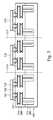
- FIG. 1 athere is shown a cross-section view of an interposer 102 with a first integrated circuit die 104 attached to a first side of the interposer 102 via a first set of conductive bumps 106 and a second integrated circuit die 108 attached to a second side of the interposer 102 via a second set of conductive bumps 110 in accordance with an embodiment.
- the first set of conductive bumps 106 and the second set of conductive bumps 110may comprise, for example, microbumps having a diameter of about 5 microns to about 50 microns.
- the interposer 102is further attached to a substrate 112 , which may be, for example, a packaging substrate, another die/wafer, a printed-circuit board, a high-density interconnect, or the like.
- a substrate 112which may be, for example, a packaging substrate, another die/wafer, a printed-circuit board, a high-density interconnect, or the like.
- Through substrate vias (TSVs) 114 in the interposer 102provide an electrical connection between the first integrated circuit die 104 and the second integrated circuit die 108 , as well as between the substrate 112 and one or both of the first integrated circuit die 104 and the second integrated circuit die 108 via a third set of conductive bumps 116 .
- TSVs 118 in the substrate 112provide an electrical connection between the third set of conductive bumps 116 and a set of conductive balls 120 , which may in turn be connected to another substrate (not shown).
- the substrate 112may be any suitable substrate, such as a 1/2/1 laminate substrate, a 4-layer laminate substrate, or the like.
- Redistribution lines (RDLs), indicated generally by lines 122 , within the substrate 112allow for a different pin configuration as well as a larger conductive ball 120 .
- the substrate 112also includes a cavity 224 such that the second integrated circuit die 108 extends into the cavity 224 formed in the underlying substrate 112 .
- the size of the third set of conductive bumpsmay be smaller than what would be possible using a substrate without a cavity, because the size of the third set of conductive bumps no longer needs to be greater than the thickness of the second integrated circuit die 108 .
- the size of the third set of conductive bumpsmay be smaller, it may be possible to increase the pin count available for a same size of interposer 102 . As a result, a thinner overall package may be possible.
- the first integrated circuit die 104 and the second integrated circuit die 108may be any suitable integrated circuit die for a particular application.
- one of the first integrated circuit die 104 and the second integrated circuit die 108may be a memory chip, such as a DRAM, SRAM, NVRAM, and/or the like, while the other die may be a logic circuit.
- the second integrated circuit die 108may comprise a DRAM die having a thickness of about 100 ⁇ m
- the third set of conductive bumps 116may have a thickness of about such as about 80 ⁇ m diameter bumps (about 60 ⁇ m collapsed).
- the third set of conductive bumps 116may be required to have a larger size, such as about 150 ⁇ m, which may collapse to have a thickness of about 120 ⁇ m.
- the larger conductive balls 120may have a diameter of about 250 ⁇ m.
- the resulting packagemay have a total height H from the conductive balls 120 to a top surface of the first integrated circuit die 104 of about 0.87 mm, as compared to a total height of about 0.93 mm when using a substrate without a cavity.
- the cavity 224may optionally be filled with a thermal pad or gap filler material 226 .
- the thermal pad 226may be a conformable material suitable to fill the gap between the second integrated circuit die 108 and the substrate 112 .
- the thermal pad 226may be a thermally conductive material to conduct heat away from the second integrated circuit die.
- the thermal pad 226is formed of a Therm-A-GapTM Gels or Interface Materials produced by Chomerics, div. of Parker Hannifin Corp. These materials may, for example, comprise an elastomer with metallic fillers. Other materials, such as a thermal interface material or a polymer may also be used.
- FIG. 1 aalso illustrates an optional heat conductive pad 228 in the substrate 112 .
- the heat conductive pad 228may be, for example, a copper pad.
- the heat conductive pad 228may have a thickness dependent upon the particular device and the need or desire for additional heat dissipation.
- FIG. 1 aillustrates an embodiment in which the heat conductive pad 228 occupies about 30% of the volume of the substrate below the second integrated circuit die 108 .
- FIGS. 1 b and 1 cillustrate embodiments in which the heat conductive pad 228 occupies a greater amount, such as 60% and 100%, respectively.
- the RDL 122 along the bottom side of the substrate 112may not extend under the second integrated circuit die 108 .
- FIG. 1 acompare the embodiment illustrated in FIG. 1 a , in which the RDL 122 extends between the cavity 224 and a bottom of the substrate 112 , to FIG. 1 c , in which the RDL 122 is omitted between the cavity 224 and a bottom of the substrate 112 due to the size of the heat conductive pad 228 .
- thermal vias 230may be used as illustrated in FIG. 1 d .
- thermal vias 230such as those illustrated in FIG. 1 d may exhibit performance characteristics similar to a 100% heat conductive pad, but with less heat conductive material (e.g., copper) content and, as a result, may be more cost effective.
- FIGS. 1 a - 1 dalso illustrate an underfill material 124 placed between the various components, e.g., the first integrated circuit die 104 , the second integrated circuit die 108 , the interposer 102 , and the substrate 112 .
- An encapsulant or overmold 126may also be formed over the components to protect the components from the environment and external contaminants.
- FIGS. 2-9illustrate a method of forming a semiconductor device such as those illustrated above with reference to FIGS. 1 a - 1 d . It should be noted that the method illustrated in FIGS. 2-9 illustrates a method in which a first die is connected to a first side of an interposer first, followed by forming conductive bumps on a second side of the interposer, placing a second die on the second side of the interposer, and finally, attaching the interposer to a substrate having a cavity formed therein. It should be appreciated that this order is provided for illustrative purposes only, and that other sequences may be used.
- the embodiment discussed belowassumes that the multiple dies are placed on each side of the interposer, and then the interposer is singulated for placement on a substrate. Other processes, including singulating the interposer prior to placing the first die and/or the second die on the interposer, may be used.
- the interposer 202comprises a substrate 206 , one or more dielectric layers 208 , interconnections 210 , contact pads 212 , and through substrate vias 214 .
- the substrate 206is similar to the doped silicon substrate used to form an integrated circuit die. While the substrate 206 may be formed of other materials, it is believed that using silicon substrates for the interposer may reduce the stress because the coefficient of thermal expansion (CTE) mismatch between the silicon substrates and the silicon typically used for the dies is lower than with substrates formed of different materials.
- CTEcoefficient of thermal expansion
- the dielectric layers 208can be an oxide dielectric or other dielectric materials in which the interconnections 210 may be formed from a conductive material such as aluminum and copper.
- the interconnections 210may include, for example, multiple layers of redistribution lines and vias interconnecting adjacent layers of redistribution lines.
- the interconnectionsmay be formed, for example, of copper, nickel, aluminum, tungsten, titanium, combinations thereof, and/or the like.
- the through substrate vias 214when completed in subsequent processing steps, provide electrically conductive pathways between the contact pads 212 on a first side of the interposer 202 and a second side of the interposer 202 , via the interconnections 210 .
- the through substrate vias 214may be formed by any appropriate method. For example, openings may be formed extending into the substrate 206 by, for example, one or more etching processes, milling, laser techniques, or the like. The openings may be lined with diffusion barrier layers, adhesion layers, isolation layers, and/or the like, and filled with a conductive material.
- the diffusion barrier layersmay comprise one or more layers of TaN, Ta, TiN, Ti, CoW, or the like, and the conductive material may comprise, for example, copper, tungsten, aluminum, silver, combinations thereof, and/or the like, formed by an electro-chemical plating process, thereby forming the through substrate vias 214 .
- interposer 202illustrates an interposer prior to dicing to form separate packages.
- lines 216illustrate boundaries, e.g., scribe lines, at which the interposer 202 may be diced upon completion.
- two contact pads 212 and two through substrate vias 214 for each packageare shown for illustrative purposes only, and that actual devices may have more or less contact pads 212 and through substrate vias 214 .
- FIG. 3illustrates placement of first dies 318 onto the interposer 202 in accordance with an embodiment.
- the first dies 318may include any suitable circuitry for a particular application.
- the first dies 318are electrically coupled to the interposer 202 in a flip-chip configuration such that contact pads on the first dies 318 face the interposer 202 .
- the contact pads of the first dies 318are electrically coupled to the contact pads on the interposer 202 via conductive bumps 320 , which may be formed by lead free solder, eutectic lead, or the like.
- An optional underfill material 322may be injected or otherwise formed in the space between the first dies 318 and the interposer 202 .
- the underfill material 322may, for example, comprise a liquid epoxy, deformable gel, silicon rubber, or the like, that is dispensed between the first dies 318 and the interposer 202 , and then cured to harden. This underfill material 322 is used, among other things, to reduce cracking in the conductive bumps 320 and to protect the joints from contaminants.
- FIG. 4illustrates attaching a carrier substrate 424 and thinning a backside of the interposer 202 in accordance with an embodiment.
- the carrier substrate 424may be attached using an adhesive 426 .
- the carrier substrate 424provides temporary mechanical and structural support during subsequent processing steps. In this manner, damage to the interposer 202 is reduced or prevented.
- the carrier substrate 424may comprise, for example, glass, silicon oxide, aluminum oxide, and the like.
- the adhesive 426may be any suitable adhesive, such as an ultraviolet (UV) glue, which loses its adhesive property when exposed to UV lights.
- UVultraviolet
- a thinning process performed on a backside of the interposer 202exposes the through substrate vias 214 .
- the thinning processmay be performed using an etching process and/or a planarization process, such as a chemical mechanical polishing (CMP) process.
- CMPchemical mechanical polishing
- a planarizing processsuch as a CMP
- one or more wet etching processes having a high etch-rate selectivity between the material of the liner and the interposer 202may be performed, thereby leaving the through substrate vias 214 protruding from the backside of the interposer 202 as illustrated in FIG.
- the etch processmay be, for example, a dry etch process using HBr/O 2 , HBr/Cl 2 /O 2 , SF 6 /CL 2 , SF 6 plasma, or the like.
- a protective layer 428such as a spin-on glass (SOG) layer is formed. Thereafter, one or more etching steps may be performed to recess the protective layer 428 and to remove the liner, if present.
- the etching processesmay have a high etch-rate selectivity between the material of the protective layer 428 /liner and the material of the through substrate vias 214 . It should be noted, however, that in other embodiments, the through substrate vias 214 may not protrude from the backside of the interposer 202 ; any suitable configuration of through substrate vias 214 and the associated interconnects may be used.
- FIG. 5illustrates formation of a stress buffer layer 530 and a backside RDL 532 in accordance with an embodiment.
- the stress buffer layer 530may be formed, for example, of a solder resist material or low-temperature polyimide deposited and etched back to expose the through substrate vias 214 . Thereafter the backside RDL 532 may be formed.
- the backside RDL 532may be formed of any suitable conductive material, such as copper, copper alloys, aluminum, silver, gold, combinations thereof, and/or the like, formed by any suitable technique, such as electro-chemical plating (ECP), electroless plating, other deposition methods such as sputtering, printing, and chemical vapor deposition (CVD) methods, or the like.
- ECPelectro-chemical plating
- CVDchemical vapor deposition
- a passivation layer 634is blanket formed and patterned to form openings, in which an under bump metallization (UBM) structure 636 and a presolder 638 are formed.
- the passivation layer 634may be formed of nitrides, oxides, polyimide, and the like.
- the openings in the passivation layer 634may be formed using photo-lithography techniques such that the openings expose portions of the backside RDL 532 .
- the UBM structures 636are formed of one or more layers of conductive materials and provide an electrical connection between the backside RDL 532 and the solder bumps to be formed in subsequent processing steps.
- the UBM structures 636may be formed, for example, of one or more layers of chrome, a chrome-copper alloy, copper, gold, titanium, titanium tungsten, nickel, combinations thereof, or the like. Once completed, the presolder may be applied to the UBM structures 636 .
- FIG. 7illustrates conductive bumps 740 placed on select ones of the UBM structures 636 in accordance with an embodiment.
- the conductive bumps 740may be formed of a eutectic solder, lead free solder, or the like.
- dieswill be attached to the UBM structures 636 to which the conductive bumps 740 have not been placed.
- the conductive bumps 740may be slightly larger than if a die were not attached on both sides of the interposer 202 , although as discussed above, the use of a cavity in the underlying substrate may reduce or eliminate the need for a larger bump size.
- the size of the UBM structures 636 coupled to the conductive bumps 740may be larger to accommodate the larger size of the conductive bumps 740 as compared to those used to attach dies in subsequent processing steps.
- FIG. 8illustrates placement of second dies 842 among the conductive bumps 740 in accordance with an embodiment.
- the second dies 842may include any suitable circuitry for a particular application.
- second dies 842are electrically coupled to the interposer 202 in a flip-chip configuration such that contact pads on the second dies 842 face the interposer 202 .
- the contact pads of the second dies 842are electrically coupled to the contact pads on the interposer via conductive bumps 844 , which may be formed by lead free solder, eutectic lead, or the like.
- An optional underfill material 846may be injected or otherwise formed in the space between second dies 842 and the interposer 202 , similar to the underfill material 322 used between the first dies 318 and the interposer 202 , to reduce cracking in the conductive bumps 740 and to protect the joints from contaminants.
- the underfill material 846may, for example, comprise a liquid epoxy, deformable gel, silicon rubber, or the like, that is dispensed between second dies 842 and the interposer 202 , and then cured to harden.
- FIG. 9illustrates the structure illustrated in FIG. 8 after the interposer 202 has been diced and attached to a substrate 952 having a cavity 954 formed therein, such as the substrate discussed above with reference to FIGS. 1 a - 1 d .
- the second die 842is positioned such that the second die 842 extends into the cavity 954 .
- the use of a substrate having a cavityallows for smaller conductive bumps 740 to be used, and hence, a smaller overall package size.
- FIG. 9also illustrates an optional heat dissipation layer 956 , which helps dissipate heat away from the second die 842 .
- the heat dissipation layer 956may, for example, comprise the thermal pad 226 , the heat conductive pad 228 , and/or the thermal vias 230 .
- the substrate 952may be formed by any suitable methods.
- embodiments such as those discussed abovemay reduce the stress between the dies and the substrate. It is believed that the reduction is due in part to the CTE mismatch being close to zero between the first die 318 , the second die 842 , and the interposer 202 , particularly when a silicon interposer is being used. This type of configuration tends to thermally isolate the first die 318 and the second die 842 from the substrate 952 . Furthermore, the connection between the substrate 952 and the interposer 202 is via conductive bumps 740 , which are generally larger. Due to the large size, the stress is dispersed over a greater area, thereby creating a stronger joint.
- FIG. 10illustrates results that may be obtained by embodiments such as those discussed herein.
- the operating temperature of a structure wherein the first die is a logic die operating at 2.0 W and the second die is a DRAM die operating at 0 . 4 Wmay be reduce from 64° C. to less than about 58° C. It should be appreciated that since the operating temperature is reduced, power consumption is also reduced.
- FIGS. 11 a and 11 billustrate a comparison between a stacked die configuration with and without an interposer, wherein the simulation scenario used a thermal cycle between 221° C. and 25° C., micro-bumps of about 20 ⁇ , and lead-free (e.g., SnAg) solder.
- FIG. 11 aillustrates stress that may be seen in a configuration in which a first die 1102 is attached to a substrate 1104 , e.g., a 1/2/1 laminate substrate, and a second die 1106 is placed directly on the first die 1102 .
- a significant amount of stressmay be seen in the connection between the first die 1102 and the second die 1106 .
- a significant amount of stressmay also be seen in the connection between the substrate 1104 and the first die 1102 .
- FIG. 11 billustrates the stress that may be seen in an embodiment such as that discussed above with reference to FIG. 1 .
- the first die 1102 and the second die 1106are connected to opposing sides of an interposer 1108 .
- the maximum amount of stress in the example illustrated in FIG. 11 amay be reduced to about 0.845 a.u. compared to a maximum stress of about 2.5 a.u., about a 66% reduction in the maximum stress level. It is believed that this reduction is due in part to the CTE mismatch being close to zero between the first die 1102 , the second die 1106 , and the interposer 1108 , particularly when a silicon interposer is being used.
- This type of configurationtends to thermally isolate the first die 1102 and the second die 1106 from the substrate 1104 .
Landscapes
- Engineering & Computer Science (AREA)
- Microelectronics & Electronic Packaging (AREA)
- Computer Hardware Design (AREA)
- Power Engineering (AREA)
- Physics & Mathematics (AREA)
- Condensed Matter Physics & Semiconductors (AREA)
- General Physics & Mathematics (AREA)
- Manufacturing & Machinery (AREA)
- Wire Bonding (AREA)
- Cooling Or The Like Of Semiconductors Or Solid State Devices (AREA)
Abstract
Description
- This application claims the benefit of U.S. Provisional Application Ser. No. 61/308,561, filed Feb. 26, 2010, and entitled “3D Semiconductor Device Using An Interposer,” which application is hereby incorporated herein by reference.
- This disclosure relates generally to semiconductor devices and, more particularly, to 3D semiconductor packages using an interposer.
- Since the invention of the integrated circuit (IC), the semiconductor industry has experienced continued rapid growth due to continuous improvements in the integration density of various electronic components (i.e., transistors, diodes, resistors, capacitors, etc.). For the most part, this improvement in integration density has come from repeated reductions in minimum feature size, which allows more components to be integrated into a given area.
- These integration improvements are essentially two-dimensional (2D) in nature, in that the volume occupied by the integrated components is essentially on the surface of the semiconductor wafer. Although dramatic improvement in lithography has resulted in considerable improvement in 2D IC formation, there are physical limits to the density that can be achieved in two dimensions. One of these limits is the minimum size needed to make these components. Also, when more devices are put into one chip, more complex designs are required.
- In an attempt to further increase circuit density, three-dimensional (3D) ICs have been investigated. In a typical formation process of a 3D IC, two dies are bonded together and electrical connections are formed between each die and contact pads on a substrate. For example, one attempt involved bonding two dies on top of each other. The stacked dies were then bonded to a carrier substrate and wire bonds electrically coupled contact pads on each die to contact pads on the carrier substrate.
- Another 3D package utilized packaging-on-packaging (PoP) or interposer techniques for stacking dies to reduce form factor. PoP typically includes one packaged die placed over another packaged die, wherein the dies are electrically coupled by solder bumps. The bottom die is then electrically coupled to a packaging substrate. PoP packages, however, are difficult to decrease the form factor. Additionally, packages utilizing an interposer are limited by the pin count to the substrate.
- These and other problems are generally reduced, solved, or circumvented, and technical advantages are generally achieved, by embodiments discussed herein, which provides a 3D semiconductor package using an interposer.
- In accordance with an embodiment, an interposer is provided having a first die electrically coupled to a first side of the interposer and a second die electrically coupled to a second side of the interposer. Conductive bumps on the interposer electrically couple the interposer to a substrate, which may be a packaging substrate, a high-density interconnect, a printed circuit board, or the like. The substrate has a cavity such that the second die, which is electrically coupled to the interposer, is positioned within the cavity. The use of a cavity may allow smaller conductive bumps to be used, thereby allowing a higher number of conductive bumps to be used. A thermal pad may be placed within the cavity and/or the substrate may comprise a heat conductive pad to aid in the dissipation of the heat from the second die.
- Other embodiments are disclosed.
- For a more complete understanding of the embodiments, and the advantages thereof, reference is now made to the following descriptions taken in conjunction with the accompanying drawings, in which:
FIGS. 1 a-1dillustrate various features and characteristics of various embodiments;FIGS. 2-9 illustrate various intermediate steps of forming an embodiment;FIG. 10 is a plot representing thermal characteristics that may be obtained with various embodiments; andFIGS. 11 aand11bcompare stress characteristics of stacked die configurations with and without an interposer.- The making and using of the embodiments of the disclosure are discussed in detail below. It should be appreciated, however, that the embodiments provide many applicable inventive concepts that can be embodied in a wide variety of specific contexts. The specific embodiments discussed are merely illustrative of specific ways to make and use the embodiments, and do not limit the scope of the disclosure.
- Referring first to
FIG. 1 a, there is shown a cross-section view of aninterposer 102 with a firstintegrated circuit die 104 attached to a first side of theinterposer 102 via a first set ofconductive bumps 106 and a secondintegrated circuit die 108 attached to a second side of theinterposer 102 via a second set ofconductive bumps 110 in accordance with an embodiment. The first set ofconductive bumps 106 and the second set ofconductive bumps 110 may comprise, for example, microbumps having a diameter of about 5 microns to about 50 microns. - The
interposer 102 is further attached to asubstrate 112, which may be, for example, a packaging substrate, another die/wafer, a printed-circuit board, a high-density interconnect, or the like. Through substrate vias (TSVs)114 in theinterposer 102 provide an electrical connection between the first integrated circuit die104 and the secondintegrated circuit die 108, as well as between thesubstrate 112 and one or both of the firstintegrated circuit die 104 and the second integrated circuit die108 via a third set ofconductive bumps 116.TSVs 118 in thesubstrate 112 provide an electrical connection between the third set ofconductive bumps 116 and a set ofconductive balls 120, which may in turn be connected to another substrate (not shown). - The
substrate 112 may be any suitable substrate, such as a 1/2/1 laminate substrate, a 4-layer laminate substrate, or the like. Redistribution lines (RDLs), indicated generally bylines 122, within thesubstrate 112 allow for a different pin configuration as well as a largerconductive ball 120. - The
substrate 112 also includes acavity 224 such that the secondintegrated circuit die 108 extends into thecavity 224 formed in theunderlying substrate 112. As a result of thecavity 224, the size of the third set of conductive bumps may be smaller than what would be possible using a substrate without a cavity, because the size of the third set of conductive bumps no longer needs to be greater than the thickness of the second integratedcircuit die 108. It should also be noted that because the size of the third set of conductive bumps may be smaller, it may be possible to increase the pin count available for a same size ofinterposer 102. As a result, a thinner overall package may be possible. - The first integrated circuit die104 and the second
integrated circuit die 108 may be any suitable integrated circuit die for a particular application. For example, one of the firstintegrated circuit die 104 and the secondintegrated circuit die 108 may be a memory chip, such as a DRAM, SRAM, NVRAM, and/or the like, while the other die may be a logic circuit. In an embodiment such as this example, the second integratedcircuit die 108 may comprise a DRAM die having a thickness of about 100 μm, the third set ofconductive bumps 116 may have a thickness of about such as about 80 μm diameter bumps (about 60 μm collapsed). In contrast, if a substrate is used without a cavity, the third set ofconductive bumps 116 may be required to have a larger size, such as about 150 μm, which may collapse to have a thickness of about 120 μm. The largerconductive balls 120 may have a diameter of about 250 μm. Thus, as a result of thecavity 224, the resulting package may have a total height H from theconductive balls 120 to a top surface of the first integratedcircuit die 104 of about 0.87 mm, as compared to a total height of about 0.93 mm when using a substrate without a cavity. - The
cavity 224 may optionally be filled with a thermal pad orgap filler material 226. Thethermal pad 226 may be a conformable material suitable to fill the gap between the second integratedcircuit die 108 and thesubstrate 112. Thethermal pad 226 may be a thermally conductive material to conduct heat away from the second integrated circuit die. In an embodiment, thethermal pad 226 is formed of a Therm-A-Gap™ Gels or Interface Materials produced by Chomerics, div. of Parker Hannifin Corp. These materials may, for example, comprise an elastomer with metallic fillers. Other materials, such as a thermal interface material or a polymer may also be used. FIG. 1 aalso illustrates an optional heatconductive pad 228 in thesubstrate 112. The heatconductive pad 228 may be, for example, a copper pad. The heatconductive pad 228 may have a thickness dependent upon the particular device and the need or desire for additional heat dissipation. For example,FIG. 1 aillustrates an embodiment in which the heatconductive pad 228 occupies about 30% of the volume of the substrate below the second integratedcircuit die 108.FIGS. 1 band1cillustrate embodiments in which the heatconductive pad 228 occupies a greater amount, such as 60% and 100%, respectively. It should be noted that depending upon the size of the heatconductive pad 228, theRDL 122 along the bottom side of thesubstrate 112 may not extend under the second integrated circuit die108. For example, compare the embodiment illustrated inFIG. 1 a, in which theRDL 122 extends between thecavity 224 and a bottom of thesubstrate 112, toFIG. 1 c, in which theRDL 122 is omitted between thecavity 224 and a bottom of thesubstrate 112 due to the size of the heatconductive pad 228.- In yet another embodiment,
thermal vias 230 may be used as illustrated inFIG. 1 d. In some embodiments,thermal vias 230 such as those illustrated inFIG. 1 dmay exhibit performance characteristics similar to a 100% heat conductive pad, but with less heat conductive material (e.g., copper) content and, as a result, may be more cost effective. FIGS. 1 a-1dalso illustrate anunderfill material 124 placed between the various components, e.g., the first integrated circuit die104, the second integrated circuit die108, theinterposer 102, and thesubstrate 112. An encapsulant orovermold 126 may also be formed over the components to protect the components from the environment and external contaminants.FIGS. 2-9 illustrate a method of forming a semiconductor device such as those illustrated above with reference toFIGS. 1 a-1d. It should be noted that the method illustrated inFIGS. 2-9 illustrates a method in which a first die is connected to a first side of an interposer first, followed by forming conductive bumps on a second side of the interposer, placing a second die on the second side of the interposer, and finally, attaching the interposer to a substrate having a cavity formed therein. It should be appreciated that this order is provided for illustrative purposes only, and that other sequences may be used. It should also be noted that the embodiment discussed below assumes that the multiple dies are placed on each side of the interposer, and then the interposer is singulated for placement on a substrate. Other processes, including singulating the interposer prior to placing the first die and/or the second die on the interposer, may be used.- Referring first to
FIG. 2 , aninterposer 202 is shown in accordance with an embodiment. In an embodiment, theinterposer 202 comprises asubstrate 206, one or moredielectric layers 208,interconnections 210,contact pads 212, and throughsubstrate vias 214. In general, thesubstrate 206 is similar to the doped silicon substrate used to form an integrated circuit die. While thesubstrate 206 may be formed of other materials, it is believed that using silicon substrates for the interposer may reduce the stress because the coefficient of thermal expansion (CTE) mismatch between the silicon substrates and the silicon typically used for the dies is lower than with substrates formed of different materials. - The
dielectric layers 208 can be an oxide dielectric or other dielectric materials in which theinterconnections 210 may be formed from a conductive material such as aluminum and copper. Theinterconnections 210 may include, for example, multiple layers of redistribution lines and vias interconnecting adjacent layers of redistribution lines. The interconnections may be formed, for example, of copper, nickel, aluminum, tungsten, titanium, combinations thereof, and/or the like. - The through
substrate vias 214, when completed in subsequent processing steps, provide electrically conductive pathways between thecontact pads 212 on a first side of theinterposer 202 and a second side of theinterposer 202, via theinterconnections 210. The throughsubstrate vias 214 may be formed by any appropriate method. For example, openings may be formed extending into thesubstrate 206 by, for example, one or more etching processes, milling, laser techniques, or the like. The openings may be lined with diffusion barrier layers, adhesion layers, isolation layers, and/or the like, and filled with a conductive material. The diffusion barrier layers, for example, may comprise one or more layers of TaN, Ta, TiN, Ti, CoW, or the like, and the conductive material may comprise, for example, copper, tungsten, aluminum, silver, combinations thereof, and/or the like, formed by an electro-chemical plating process, thereby forming the throughsubstrate vias 214. - It should be noted that the
interposer 202 illustrates an interposer prior to dicing to form separate packages. InFIG. 2 ,lines 216 illustrate boundaries, e.g., scribe lines, at which theinterposer 202 may be diced upon completion. It should also be noted that twocontact pads 212 and two throughsubstrate vias 214 for each package are shown for illustrative purposes only, and that actual devices may have more orless contact pads 212 and throughsubstrate vias 214. FIG. 3 illustrates placement of first dies318 onto theinterposer 202 in accordance with an embodiment. The first dies318 may include any suitable circuitry for a particular application. In an embodiment, the first dies318 are electrically coupled to theinterposer 202 in a flip-chip configuration such that contact pads on the first dies318 face theinterposer 202. The contact pads of the first dies318 are electrically coupled to the contact pads on theinterposer 202 viaconductive bumps 320, which may be formed by lead free solder, eutectic lead, or the like.- An
optional underfill material 322 may be injected or otherwise formed in the space between the first dies318 and theinterposer 202. Theunderfill material 322 may, for example, comprise a liquid epoxy, deformable gel, silicon rubber, or the like, that is dispensed between the first dies318 and theinterposer 202, and then cured to harden. Thisunderfill material 322 is used, among other things, to reduce cracking in theconductive bumps 320 and to protect the joints from contaminants. FIG. 4 illustrates attaching acarrier substrate 424 and thinning a backside of theinterposer 202 in accordance with an embodiment. Thecarrier substrate 424 may be attached using an adhesive426. Generally, thecarrier substrate 424 provides temporary mechanical and structural support during subsequent processing steps. In this manner, damage to theinterposer 202 is reduced or prevented. Thecarrier substrate 424 may comprise, for example, glass, silicon oxide, aluminum oxide, and the like. The adhesive426 may be any suitable adhesive, such as an ultraviolet (UV) glue, which loses its adhesive property when exposed to UV lights.- After attaching the
carrier substrate 424 to theinterposer 202, a thinning process performed on a backside of theinterposer 202 exposes the throughsubstrate vias 214. The thinning process may be performed using an etching process and/or a planarization process, such as a chemical mechanical polishing (CMP) process. For example, initially a planarizing process, such as a CMP, may be performed to initially expose the liner of the throughsubstrate vias 214. Thereafter, one or more wet etching processes having a high etch-rate selectivity between the material of the liner and theinterposer 202 may be performed, thereby leaving the throughsubstrate vias 214 protruding from the backside of theinterposer 202 as illustrated inFIG. 4 . In embodiments in which theinterposer 202 comprises silicon, the etch process may be, for example, a dry etch process using HBr/O2, HBr/Cl2/O2, SF6/CL2, SF6plasma, or the like. - After recessing the backside of the
interposer 202, aprotective layer 428, such as a spin-on glass (SOG) layer is formed. Thereafter, one or more etching steps may be performed to recess theprotective layer 428 and to remove the liner, if present. The etching processes may have a high etch-rate selectivity between the material of theprotective layer 428/liner and the material of the throughsubstrate vias 214. It should be noted, however, that in other embodiments, the throughsubstrate vias 214 may not protrude from the backside of theinterposer 202; any suitable configuration of throughsubstrate vias 214 and the associated interconnects may be used. FIG. 5 illustrates formation of astress buffer layer 530 and abackside RDL 532 in accordance with an embodiment. Thestress buffer layer 530 may be formed, for example, of a solder resist material or low-temperature polyimide deposited and etched back to expose the throughsubstrate vias 214. Thereafter thebackside RDL 532 may be formed. Thebackside RDL 532 may be formed of any suitable conductive material, such as copper, copper alloys, aluminum, silver, gold, combinations thereof, and/or the like, formed by any suitable technique, such as electro-chemical plating (ECP), electroless plating, other deposition methods such as sputtering, printing, and chemical vapor deposition (CVD) methods, or the like. A mask (not shown) may also be used.- Next, as shown in
FIG. 6 , apassivation layer 634 is blanket formed and patterned to form openings, in which an under bump metallization (UBM)structure 636 and apresolder 638 are formed. Thepassivation layer 634 may be formed of nitrides, oxides, polyimide, and the like. The openings in thepassivation layer 634 may be formed using photo-lithography techniques such that the openings expose portions of thebackside RDL 532. TheUBM structures 636 are formed of one or more layers of conductive materials and provide an electrical connection between thebackside RDL 532 and the solder bumps to be formed in subsequent processing steps. TheUBM structures 636 may be formed, for example, of one or more layers of chrome, a chrome-copper alloy, copper, gold, titanium, titanium tungsten, nickel, combinations thereof, or the like. Once completed, the presolder may be applied to theUBM structures 636. FIG. 7 illustratesconductive bumps 740 placed on select ones of theUBM structures 636 in accordance with an embodiment. Theconductive bumps 740 may be formed of a eutectic solder, lead free solder, or the like. As will be discussed in greater detail below, dies will be attached to theUBM structures 636 to which theconductive bumps 740 have not been placed. In order to allow room for the dies, theconductive bumps 740 may be slightly larger than if a die were not attached on both sides of theinterposer 202, although as discussed above, the use of a cavity in the underlying substrate may reduce or eliminate the need for a larger bump size. The size of theUBM structures 636 coupled to theconductive bumps 740 may be larger to accommodate the larger size of theconductive bumps 740 as compared to those used to attach dies in subsequent processing steps.FIG. 8 illustrates placement of second dies842 among theconductive bumps 740 in accordance with an embodiment. The second dies842 may include any suitable circuitry for a particular application. In an embodiment, second dies842 are electrically coupled to theinterposer 202 in a flip-chip configuration such that contact pads on the second dies842 face theinterposer 202. The contact pads of the second dies842 are electrically coupled to the contact pads on the interposer viaconductive bumps 844, which may be formed by lead free solder, eutectic lead, or the like.- An
optional underfill material 846 may be injected or otherwise formed in the space between second dies842 and theinterposer 202, similar to theunderfill material 322 used between the first dies318 and theinterposer 202, to reduce cracking in theconductive bumps 740 and to protect the joints from contaminants. Theunderfill material 846 may, for example, comprise a liquid epoxy, deformable gel, silicon rubber, or the like, that is dispensed between second dies842 and theinterposer 202, and then cured to harden. FIG. 9 illustrates the structure illustrated inFIG. 8 after theinterposer 202 has been diced and attached to asubstrate 952 having acavity 954 formed therein, such as the substrate discussed above with reference toFIGS. 1 a-1d. In this embodiment, thesecond die 842 is positioned such that thesecond die 842 extends into thecavity 954. As discussed above, the use of a substrate having a cavity allows for smallerconductive bumps 740 to be used, and hence, a smaller overall package size.FIG. 9 also illustrates an optionalheat dissipation layer 956, which helps dissipate heat away from thesecond die 842. Theheat dissipation layer 956 may, for example, comprise thethermal pad 226, the heatconductive pad 228, and/or thethermal vias 230. Thesubstrate 952 may be formed by any suitable methods.- It has been found that embodiments such as those discussed above may reduce the stress between the dies and the substrate. It is believed that the reduction is due in part to the CTE mismatch being close to zero between the
first die 318, thesecond die 842, and theinterposer 202, particularly when a silicon interposer is being used. This type of configuration tends to thermally isolate thefirst die 318 and thesecond die 842 from thesubstrate 952. Furthermore, the connection between thesubstrate 952 and theinterposer 202 is viaconductive bumps 740, which are generally larger. Due to the large size, the stress is dispersed over a greater area, thereby creating a stronger joint. - It has also been found that embodiments such as those discussed above may reduce the operating temperature of the semiconductor device, particularly when both the thermal pad and thermal heat sink are used. For example,
FIG. 10 illustrates results that may be obtained by embodiments such as those discussed herein. As illustrated inFIG. 10 , the operating temperature of a structure wherein the first die is a logic die operating at 2.0 W and the second die is a DRAM die operating at0.4 W may be reduce from 64° C. to less than about 58° C. It should be appreciated that since the operating temperature is reduced, power consumption is also reduced. FIGS. 11 aand11billustrate a comparison between a stacked die configuration with and without an interposer, wherein the simulation scenario used a thermal cycle between 221° C. and 25° C., micro-bumps of about 20 μ, and lead-free (e.g., SnAg) solder. In particular,FIG. 11 aillustrates stress that may be seen in a configuration in which afirst die 1102 is attached to asubstrate 1104, e.g., a 1/2/1 laminate substrate, and asecond die 1106 is placed directly on thefirst die 1102. As can be seen, a significant amount of stress may be seen in the connection between thefirst die 1102 and thesecond die 1106. A significant amount of stress may also be seen in the connection between thesubstrate 1104 and thefirst die 1102.- In comparison,
FIG. 11 billustrates the stress that may be seen in an embodiment such as that discussed above with reference toFIG. 1 . In this case thefirst die 1102 and thesecond die 1106 are connected to opposing sides of aninterposer 1108. As a result of this type of configuration, the maximum amount of stress in the example illustrated inFIG. 11 amay be reduced to about 0.845 a.u. compared to a maximum stress of about 2.5 a.u., about a 66% reduction in the maximum stress level. It is believed that this reduction is due in part to the CTE mismatch being close to zero between thefirst die 1102, thesecond die 1106, and theinterposer 1108, particularly when a silicon interposer is being used. This type of configuration tends to thermally isolate thefirst die 1102 and thesecond die 1106 from thesubstrate 1104. - While these results do not utilize a cavity as discussed above with reference to
FIGS. 1 a-1d, it is expected that the use of a substrate with a cavity will have similar stress characteristics, but with a smaller overall package size. - Although the present disclosure and its advantages have been described in detail, it should be understood that various changes, substitutions, and alterations can be made herein without departing from the spirit and scope of the embodiments as defined by the appended claims. Moreover, the scope of the present application is not intended to be limited to the particular embodiments of the process, machine, manufacture, composition of matter, means, methods, and steps described in the specification. As one of ordinary skill in the art will readily appreciate from the disclosure, processes, machines, manufacture, compositions of matter, means, methods, or steps, presently existing or later to be developed, that perform substantially the same function or achieve substantially the same result as the corresponding embodiments described herein may be utilized according to the present disclosure. Accordingly, the appended claims are intended to include within their scope such processes, machines, manufacture, compositions of matter, means, methods, or steps.
Claims (20)
1. A semiconductor device comprising:
a first die;
a second die;
an interposer, the first die being electrically coupled to a first side of the interposer, the second die being electrically coupled to a second side of the interposer; and
a substrate, the substrate being electrically coupled to the second side of the interposer, wherein the substrate includes a cavity, the second die being positioned within the cavity.
2. The semiconductor device ofclaim 1 , further comprising a thermal pad layer along a bottom of the cavity.
3. The semiconductor device ofclaim 1 , wherein the substrate further comprises a heat conductive layer under the cavity.
4. The semiconductor device ofclaim 3 , wherein the heat conductive layer extends from a surface of the cavity to an opposing side of the substrate.
5. The semiconductor device ofclaim 1 , wherein the substrate is electrically coupled to the second side of the interposer using solder bumps having a diameter of 80 μm or less.
6. The semiconductor device ofclaim 5 , wherein the solder bumps have a collapsed height of 60 μm or less.
7. The semiconductor device ofclaim 1 , wherein the interposer is a silicon interposer.
8. The semiconductor device ofclaim 1 , wherein the substrate is a 1/2/1 laminate substrate.
9. The semiconductor device ofclaim 1 , wherein one of the first die and the second die comprises a logic circuit and the other of the first die and the second die is a memory.
10. A semiconductor device comprising:
an interposer having bond pads on a first side and a second side;
a first die attached to the bond pads on the first side of the interposer by a first plurality of conductive bumps;
a second die attached to the bond pads on the second side of the interposer by a second plurality of conductive bumps; and
a substrate, the substrate being attached to the bond pads on the second side of the interposer by a third plurality of conductive bumps, the substrate having a cavity, the second die being positioned within the cavity.
11. The semiconductor device ofclaim 10 , further comprising a thermal gap filler material in the cavity between the second die and the substrate.
12. The semiconductor device ofclaim 10 , wherein the substrate further comprises a heat conductive layer under the cavity.
13. The semiconductor device ofclaim 12 , wherein the heat conductive layer extends from a surface of the cavity to an opposing side of the substrate.
14. The semiconductor device ofclaim 10 , wherein the interposer is a silicon interposer.
15. The semiconductor device ofclaim 10 , wherein the substrate is a 1/2/1 laminate substrate.
16. A method of forming a semiconductor device, the method comprising:
providing one or more first dies;
providing one or more second dies;
providing an interposer, the interposer having bond pads on a first side and a second side;
attaching the one or more first dies to the first side of the interposer using conductive bumps;
attaching the one or more second dies to the second side of the interposer using conductive bumps; and
attaching the interposer to a substrate such that at least one of the one or more second dies is positioned within a cavity in the substrate.
17. The method ofclaim 16 , further comprising attaching a carrier substrate to the first side of the interposer and the one or more first dies prior to the attaching one or more second dies and removing the carrier substrate after the attaching one or more second dies.
18. The method ofclaim 16 , further comprising forming a thermal pad layer in the cavity.
19. The method ofclaim 16 , wherein the substrate includes a heat conductive pad layer under the cavity.
20. The method ofclaim 19 , wherein the heat conductive pad layer extends from the cavity to an opposing side of the substrate.
Priority Applications (7)
| Application Number | Priority Date | Filing Date | Title |
|---|---|---|---|
| US12/813,212US8519537B2 (en) | 2010-02-26 | 2010-06-10 | 3D semiconductor package interposer with die cavity |
| TW099131598ATWI415244B (en) | 2010-02-26 | 2010-09-17 | Semiconductor device and method for forming the same |
| CN2010105021415ACN102169875B (en) | 2010-02-26 | 2010-09-30 | Semiconductor device and manufacturing method thereof |
| US13/899,815US8865521B2 (en) | 2010-02-26 | 2013-05-22 | 3D semiconductor package interposer with die cavity |
| US14/249,637US9385095B2 (en) | 2010-02-26 | 2014-04-10 | 3D semiconductor package interposer with die cavity |
| US15/154,770US9780072B2 (en) | 2010-02-26 | 2016-05-13 | 3D semiconductor package interposer with die cavity |
| US15/722,983US10446520B2 (en) | 2010-02-26 | 2017-10-02 | 3D semiconductor package interposer with die cavity |
Applications Claiming Priority (2)
| Application Number | Priority Date | Filing Date | Title |
|---|---|---|---|
| US30856110P | 2010-02-26 | 2010-02-26 | |
| US12/813,212US8519537B2 (en) | 2010-02-26 | 2010-06-10 | 3D semiconductor package interposer with die cavity |
Related Child Applications (1)
| Application Number | Title | Priority Date | Filing Date |
|---|---|---|---|
| US13/899,815DivisionUS8865521B2 (en) | 2010-02-26 | 2013-05-22 | 3D semiconductor package interposer with die cavity |
Publications (2)
| Publication Number | Publication Date |
|---|---|
| US20110210444A1true US20110210444A1 (en) | 2011-09-01 |
| US8519537B2 US8519537B2 (en) | 2013-08-27 |
Family
ID=44504861
Family Applications (2)
| Application Number | Title | Priority Date | Filing Date |
|---|---|---|---|
| US12/813,212Active2030-09-01US8519537B2 (en) | 2010-02-26 | 2010-06-10 | 3D semiconductor package interposer with die cavity |
| US13/899,815ActiveUS8865521B2 (en) | 2010-02-26 | 2013-05-22 | 3D semiconductor package interposer with die cavity |
Family Applications After (1)
| Application Number | Title | Priority Date | Filing Date |
|---|---|---|---|
| US13/899,815ActiveUS8865521B2 (en) | 2010-02-26 | 2013-05-22 | 3D semiconductor package interposer with die cavity |
Country Status (2)
| Country | Link |
|---|---|
| US (2) | US8519537B2 (en) |
| TW (1) | TWI415244B (en) |
Cited By (66)
| Publication number | Priority date | Publication date | Assignee | Title |
|---|---|---|---|---|
| US20110089552A1 (en)* | 2009-10-16 | 2011-04-21 | Park Hyungsang | Integrated circuit packaging system with package-on-package stacking and method of manufacture thereof |
| US20120106117A1 (en)* | 2010-11-02 | 2012-05-03 | Georgia Tech Research Corporation | Ultra-thin interposer assemblies with through vias |
| US20120214302A1 (en)* | 2011-02-21 | 2012-08-23 | Jeong Seyoung | Semiconductor devices and methods of fabricating the same |
| US20130082372A1 (en)* | 2011-09-30 | 2013-04-04 | Taiwan Semiconductor Manufacturing Company, Ltd. | Package on Packaging Structure and Methods of Making Same |
| WO2013066799A1 (en)* | 2011-11-04 | 2013-05-10 | Ati Technologies Ulc | Semiconductor substrate with molded support layer |
| WO2013137710A1 (en)* | 2012-03-13 | 2013-09-19 | Intel Corporation (A Corporation Of Delaware) | Microelectronic device attachment on a reverse microelectronic package |
| US20140004647A1 (en)* | 2011-06-09 | 2014-01-02 | Optiz, Inc. | Method Of Forming 3D Integrated Microelectronic Assembly With Stress Reducing Interconnects |
| US20140106508A1 (en)* | 2010-03-18 | 2014-04-17 | Marvell World Trade Ltd. | Structures embedded within core material and methods of manufacturing thereof |
| US20140252561A1 (en)* | 2013-03-08 | 2014-09-11 | Qualcomm Incorporated | Via-enabled package-on-package |
| US20140319696A1 (en)* | 2013-04-30 | 2014-10-30 | Taiwan Semiconductor Manufacturing Company, Ltd. | 3D Packages and Methods for Forming the Same |
| US8905632B2 (en) | 2011-11-29 | 2014-12-09 | Cisco Technology, Inc. | Interposer configuration with thermally isolated regions for temperature-sensitive opto-electronic components |
| US20150031184A1 (en)* | 2013-01-23 | 2015-01-29 | Taiwan Semiconductor Manufacturing Company, Ltd. | Methods of manufacturing a package |
| US20150083601A1 (en)* | 2013-09-25 | 2015-03-26 | Seagate Technology Llc | Near field transducers including electrodeposited plasmonic materials and methods of forming |
| US9018040B2 (en) | 2013-09-30 | 2015-04-28 | International Business Machines Corporation | Power distribution for 3D semiconductor package |
| US20150162258A1 (en)* | 2013-12-11 | 2015-06-11 | Taiwan Semiconductor Manufacturing Company, Ltd. | Underfill Pattern with Gap |
| WO2014180316A3 (en)* | 2013-05-10 | 2015-07-09 | Huawei Technologies Co., Ltd. | Thermal management in2.5d semiconductor packaging cross-reference to related applications |
| EP2887393A3 (en)* | 2013-12-19 | 2015-11-25 | Broadcom Corporation | Compliant dielectric layer for semiconductor device |
| US20160013235A1 (en)* | 2012-09-07 | 2016-01-14 | Taiwan Semiconductor Manufacturing Company, Ltd. | Methods and Apparatus for Sensor Module |
| US20160035632A1 (en)* | 2014-01-21 | 2016-02-04 | International Business Machines Corporation | Semiconductor tsv device package to which other semiconductor device package can be later attached |
| US9257412B2 (en)* | 2012-09-12 | 2016-02-09 | Taiwan Semiconductor Manufacturing Company, Ltd. | Stress reduction apparatus |
| WO2016032804A1 (en)* | 2014-08-26 | 2016-03-03 | Xilinx, Inc. | Multi-chip silicon substrate-less chip packaging |
| WO2016089844A1 (en)* | 2014-12-04 | 2016-06-09 | Invensas Corporation | Encapsulated integrated circuit assembly with interposer and manufacturing method thereof |
| US20160240457A1 (en)* | 2015-02-18 | 2016-08-18 | Altera Corporation | Integrated circuit packages with dual-sided stacking structure |
| US9449945B2 (en) | 2013-03-08 | 2016-09-20 | Taiwan Semiconductor Manufacturing Company, Ltd. | Filter and capacitor using redistribution layer and micro bump layer |
| US9460990B1 (en)* | 2015-04-13 | 2016-10-04 | SK Hynix Inc. | Substrates and semiconductor packages including the same, electronic systems including the semiconductor packages, and memory cards including the semiconductor packages |
| US20160343648A1 (en)* | 2015-05-22 | 2016-11-24 | Volkswagen Ag | Interposer and semiconductor module for use in automotive applicatons |
| US9526175B2 (en) | 2012-04-24 | 2016-12-20 | Intel Corporation | Suspended inductor microelectronic structures |
| US20170047309A1 (en)* | 2015-08-12 | 2017-02-16 | Samsung Electronics Co., Ltd. | Fabricating method of semiconductor device |
| FR3046697A1 (en)* | 2016-01-08 | 2017-07-14 | St Microelectronics Crolles 2 Sas | THREE-DIMENSIONAL INTEGRATED PHOTONIC STRUCTURE WITH IMPROVED OPTICAL PROPERTIES |
| US20170250166A1 (en)* | 2014-02-14 | 2017-08-31 | Taiwan Semiconductor Manufacturing Company, Ltd. | Thermal performance structure for semiconductor packages and method of forming same |
| US20170265306A1 (en)* | 2012-03-13 | 2017-09-14 | Intel Corporation | Microelectronic device attachment on a reverse microelectronic package |
| US9768090B2 (en) | 2014-02-14 | 2017-09-19 | Taiwan Semiconductor Manufacturing Company, Ltd. | Substrate design for semiconductor packages and method of forming same |
| US20170278779A1 (en)* | 2016-03-23 | 2017-09-28 | Dyi-chung Hu | Package substrate with embedded circuit |
| US9780072B2 (en) | 2010-02-26 | 2017-10-03 | Taiwan Semiconductor Manufacturing Company, Ltd. | 3D semiconductor package interposer with die cavity |
| CN107611045A (en)* | 2017-09-29 | 2018-01-19 | 中芯长电半导体(江阴)有限公司 | A kind of three-dimensional chip encapsulating structure and its method for packing |
| US20180082981A1 (en)* | 2016-09-19 | 2018-03-22 | General Electric Company | Integrated circuit devices and methods of assembling the same |
| US9935090B2 (en) | 2014-02-14 | 2018-04-03 | Taiwan Semiconductor Manufacturing Company, Ltd. | Substrate design for semiconductor packages and method of forming same |
| WO2018063512A1 (en)* | 2016-09-30 | 2018-04-05 | Intel IP Corporation | Interconnect structure for a microelectronic device |
| US10026671B2 (en) | 2014-02-14 | 2018-07-17 | Taiwan Semiconductor Manufacturing Company, Ltd. | Substrate design for semiconductor packages and method of forming same |
| US10056267B2 (en) | 2014-02-14 | 2018-08-21 | Taiwan Semiconductor Manufacturing Company, Ltd. | Substrate design for semiconductor packages and method of forming same |
| JP2018133382A (en)* | 2017-02-14 | 2018-08-23 | 三菱電機株式会社 | Semiconductor package |
| US20180374827A1 (en)* | 2015-05-27 | 2018-12-27 | Bridge Semiconductor Corporation | Semiconductor assembly with three dimensional integration and method of making the same |
| US20180374821A1 (en)* | 2017-06-23 | 2018-12-27 | Taiwan Semiconductor Manufacturing Company Ltd. | Semiconductor structure and manufacturing method thereof |
| TWI648802B (en)* | 2016-09-02 | 2019-01-21 | 美商R&D線路公司 | Method and structure of 3D wire module |
| US20190074264A1 (en)* | 2017-09-07 | 2019-03-07 | Advanced Semiconductor Engineering, Inc. | Semiconductor package structure and method for manufacturing the same |
| CN109935604A (en)* | 2019-02-26 | 2019-06-25 | 厦门云天半导体科技有限公司 | A kind of integrate is routed three-dimensional chip encapsulating structure of pinboard and preparation method thereof again |
| US10361177B2 (en)* | 2017-08-28 | 2019-07-23 | Samsung Electronics Co., Ltd | Semiconductor package having a molding layer including a molding cavity and method of fabricating the same |
| US20190304959A1 (en)* | 2018-03-29 | 2019-10-03 | Taiwan Semiconductor Manufacturing Company, Ltd. | Electronics Card Including Multi-Chip Module |
| US20190355680A1 (en)* | 2018-05-21 | 2019-11-21 | Taiwan Semiconductor Manufacturing Company, Ltd. | Semiconductor Device and Method of Manufacture |
| US10629522B2 (en) | 2017-02-08 | 2020-04-21 | Micron Technology, Inc. | Semiconductor package and method for fabricating the same |
| EP3644359A1 (en)* | 2018-10-23 | 2020-04-29 | AT & S Austria Technologie & Systemtechnik Aktiengesellschaft | Z-axis interconnection with protruding component |
| US10840134B2 (en) | 2016-03-02 | 2020-11-17 | Taiwan Semiconductor Manufacturing Company, Ltd. | Interconnect structure and method |
| KR20210017857A (en)* | 2019-08-09 | 2021-02-17 | 삼성전기주식회사 | Electronic component module and manufacturing method thereof |
| US11083086B2 (en)* | 2018-02-07 | 2021-08-03 | Ibiden Co., Ltd. | Printed wiring board and method for manufacturing printed wiring board |
| KR20210128899A (en)* | 2020-04-16 | 2021-10-27 | 타이완 세미콘덕터 매뉴팩쳐링 컴퍼니 리미티드 | Semicondutor packages and methods of forming same |
| US11183461B2 (en)* | 2016-11-29 | 2021-11-23 | Taiwan Semiconductor Manufacturing Company Ltd. | Semiconductor structure and manufacturing method thereof |
| US11374127B2 (en) | 2016-08-02 | 2022-06-28 | Taiwan Semiconductor Manufacturing Company, Ltd. | Multi-layer film device and method |
| US20220301889A1 (en)* | 2014-06-13 | 2022-09-22 | Taiwan Semiconductor Manufacturing Co., Ltd. | Integrated Circuit Packages and Methods of Forming Same |
| US11488842B2 (en)* | 2014-04-02 | 2022-11-01 | Taiwan Semiconductor Manufacturing Company, Ltd. | Method of making semiconductor device package including conformal metal cap contacting each semiconductor die |
| US20220415810A1 (en)* | 2018-09-07 | 2022-12-29 | Advanced Semiconductor Engineering, Inc. | Semiconductor device package |
| US11776917B2 (en)* | 2020-07-16 | 2023-10-03 | Advanced Semiconductor Engineering Korea, Inc. | Electronic package |
| DE102014019634B4 (en) | 2014-01-17 | 2023-10-19 | Taiwan Semiconductor Mfg. Co., Ltd. | Integrated circuit package and method of forming same |
| US11798932B2 (en) | 2011-08-16 | 2023-10-24 | Intel Corporation | Offset interposers for large-bottom packages and large-die package-on-package structures |
| US20230421117A1 (en)* | 2022-06-24 | 2023-12-28 | Wolfspeed, Inc. | Packages with backside mounted die and exposed die interconnects and methods of fabricating the same |
| US11901274B2 (en)* | 2015-09-25 | 2024-02-13 | Intel Corporation | Packaged integrated circuit device with recess structure |
| US12119282B2 (en) | 2018-09-07 | 2024-10-15 | Advanced Semiconductor Engineering, Inc. | Method of making a semiconductor device package |
Families Citing this family (56)
| Publication number | Priority date | Publication date | Assignee | Title |
|---|---|---|---|---|
| SG130055A1 (en) | 2005-08-19 | 2007-03-20 | Micron Technology Inc | Microelectronic devices, stacked microelectronic devices, and methods for manufacturing microelectronic devices |
| US9502360B2 (en)* | 2012-01-11 | 2016-11-22 | Taiwan Semiconductor Manufacturing Company, Ltd. | Stress compensation layer for 3D packaging |
| CN103620776B (en)* | 2012-01-30 | 2017-02-08 | 松下电器产业株式会社 | Semiconductor device |
| US8749072B2 (en)* | 2012-02-24 | 2014-06-10 | Broadcom Corporation | Semiconductor package with integrated selectively conductive film interposer |
| US9026872B2 (en)* | 2012-08-16 | 2015-05-05 | Xilinx, Inc. | Flexible sized die for use in multi-die integrated circuit |
| TWI497616B (en)* | 2012-11-08 | 2015-08-21 | 矽品精密工業股份有限公司 | Method of forming semiconductor package |
| US9030017B2 (en)* | 2012-11-13 | 2015-05-12 | Invensas Corporation | Z-connection using electroless plating |
| US9196575B1 (en)* | 2013-02-04 | 2015-11-24 | Altera Corporation | Integrated circuit package with cavity in substrate |
| JP6207190B2 (en)* | 2013-03-22 | 2017-10-04 | ルネサスエレクトロニクス株式会社 | Manufacturing method of semiconductor device |
| US9547034B2 (en) | 2013-07-03 | 2017-01-17 | Xilinx, Inc. | Monolithic integrated circuit die having modular die regions stitched together |
| EP3019442A4 (en) | 2013-07-08 | 2017-01-25 | Motion Engine Inc. | Mems device and method of manufacturing |
| US10273147B2 (en) | 2013-07-08 | 2019-04-30 | Motion Engine Inc. | MEMS components and method of wafer-level manufacturing thereof |
| US20150014852A1 (en)* | 2013-07-12 | 2015-01-15 | Yueli Liu | Package assembly configurations for multiple dies and associated techniques |
| WO2015013828A1 (en) | 2013-08-02 | 2015-02-05 | Motion Engine Inc. | Mems motion sensor and method of manufacturing |
| WO2015103688A1 (en) | 2014-01-09 | 2015-07-16 | Motion Engine Inc. | Integrated mems system |
| US10038259B2 (en)* | 2014-02-06 | 2018-07-31 | Xilinx, Inc. | Low insertion loss package pin structure and method |
| US9401287B2 (en) | 2014-02-07 | 2016-07-26 | Altera Corporation | Methods for packaging integrated circuits |
| US10354984B2 (en) | 2015-05-27 | 2019-07-16 | Bridge Semiconductor Corporation | Semiconductor assembly with electromagnetic shielding and thermally enhanced characteristics and method of making the same |
| US10121768B2 (en) | 2015-05-27 | 2018-11-06 | Bridge Semiconductor Corporation | Thermally enhanced face-to-face semiconductor assembly with built-in heat spreader and method of making the same |
| US11291146B2 (en) | 2014-03-07 | 2022-03-29 | Bridge Semiconductor Corp. | Leadframe substrate having modulator and crack inhibiting structure and flip chip assembly using the same |
| US9355997B2 (en) | 2014-03-12 | 2016-05-31 | Invensas Corporation | Integrated circuit assemblies with reinforcement frames, and methods of manufacture |
| US20150262902A1 (en) | 2014-03-12 | 2015-09-17 | Invensas Corporation | Integrated circuits protected by substrates with cavities, and methods of manufacture |
| US20170030788A1 (en) | 2014-04-10 | 2017-02-02 | Motion Engine Inc. | Mems pressure sensor |
| US9165793B1 (en) | 2014-05-02 | 2015-10-20 | Invensas Corporation | Making electrical components in handle wafers of integrated circuit packages |
| WO2015184531A1 (en) | 2014-06-02 | 2015-12-10 | Motion Engine Inc. | Multi-mass mems motion sensor |
| US9741649B2 (en) | 2014-06-04 | 2017-08-22 | Invensas Corporation | Integrated interposer solutions for 2D and 3D IC packaging |
| US9412806B2 (en) | 2014-06-13 | 2016-08-09 | Invensas Corporation | Making multilayer 3D capacitors using arrays of upstanding rods or ridges |
| US9915869B1 (en) | 2014-07-01 | 2018-03-13 | Xilinx, Inc. | Single mask set used for interposer fabrication of multiple products |
| RU2659980C2 (en)* | 2014-07-02 | 2018-07-04 | Интел Корпорейшн | Electronic assembly, which includes the electronic devices that are stacked onto each other |
| US9252127B1 (en) | 2014-07-10 | 2016-02-02 | Invensas Corporation | Microelectronic assemblies with integrated circuits and interposers with cavities, and methods of manufacture |
| KR102198858B1 (en) | 2014-07-24 | 2021-01-05 | 삼성전자 주식회사 | Semiconductor package stack structure having interposer substrate |
| US9373564B2 (en) | 2014-08-07 | 2016-06-21 | Industrial Technology Research Institute | Semiconductor device, manufacturing method and stacking structure thereof |
| KR102307490B1 (en)* | 2014-10-27 | 2021-10-05 | 삼성전자주식회사 | Semiconductor package |
| US11287486B2 (en) | 2014-12-09 | 2022-03-29 | Motion Engine, Inc. | 3D MEMS magnetometer and associated methods |
| CN105518860A (en)* | 2014-12-19 | 2016-04-20 | 英特尔Ip公司 | Stack type semiconductor device package with improved interconnection bandwidth |
| RU2584575C1 (en)* | 2014-12-25 | 2016-05-20 | Общество с ограниченной ответственностью "ЗЕЛНАС" | Interposer and method of making same |
| CA3220839A1 (en) | 2015-01-15 | 2016-07-21 | Motion Engine Inc. | 3d mems device with hermetic cavity |
| US9564416B2 (en) | 2015-02-13 | 2017-02-07 | Taiwan Semiconductor Manufacturing Company, Ltd. | Package structures and methods of forming the same |
| US9478500B2 (en)* | 2015-02-17 | 2016-10-25 | Advanced Semiconductor Engineering, Inc. | Interposer substrate, semiconductor structure and fabricating process thereof |
| US9711488B2 (en)* | 2015-03-13 | 2017-07-18 | Mediatek Inc. | Semiconductor package assembly |
| US9543192B2 (en)* | 2015-05-18 | 2017-01-10 | Globalfoundries Singapore Pte. Ltd. | Stitched devices |
| US9478504B1 (en) | 2015-06-19 | 2016-10-25 | Invensas Corporation | Microelectronic assemblies with cavities, and methods of fabrication |
| US10096573B2 (en) | 2015-07-28 | 2018-10-09 | Bridge Semiconductor Corporation | Face-to-face semiconductor assembly having semiconductor device in dielectric recess |
| US10269767B2 (en) | 2015-07-31 | 2019-04-23 | Taiwan Semiconductor Manufacturing Company, Ltd. | Multi-chip packages with multi-fan-out scheme and methods of manufacturing the same |
| US9881850B2 (en)* | 2015-09-18 | 2018-01-30 | Taiwan Semiconductor Manufacturing Company, Ltd. | Package structures and method of forming the same |
| KR102413441B1 (en) | 2015-11-12 | 2022-06-28 | 삼성전자주식회사 | Semiconductor package |
| US10504874B2 (en)* | 2016-08-01 | 2019-12-10 | Taiwan Semiconductor Manufacturing Company Limited | Structures and methods for providing electrical isolation in semiconductor devices |
| US10658334B2 (en)* | 2016-08-18 | 2020-05-19 | Taiwan Semiconductor Manufacturing Co., Ltd. | Method for forming a package structure including a package layer surrounding first connectors beside an integrated circuit die and second connectors below the integrated circuit die |
| KR20190056190A (en) | 2017-11-16 | 2019-05-24 | 에스케이하이닉스 주식회사 | Semiconductor package with thermal transfer plate and method manufacturing the same |
| US11264332B2 (en) | 2018-11-28 | 2022-03-01 | Micron Technology, Inc. | Interposers for microelectronic devices |
| US11476241B2 (en)* | 2019-03-19 | 2022-10-18 | Micron Technology, Inc. | Interposer, microelectronic device assembly including same and methods of fabrication |
| US11610864B2 (en) | 2019-09-09 | 2023-03-21 | Taiwan Semiconductor Manufacturing Co., Ltd. | Chip package structure and method of forming the same |
| US11164855B2 (en)* | 2019-09-17 | 2021-11-02 | Taiwan Semiconductor Manufacturing Company, Ltd. | Package structure with a heat dissipating element and method of manufacturing the same |
| KR102816598B1 (en) | 2020-09-04 | 2025-06-04 | 삼성전자주식회사 | Semiconductor package and method of manufacturing the same |
| CN112234026A (en)* | 2020-10-14 | 2021-01-15 | 天津津航计算技术研究所 | 3D chip package |
| US11502060B2 (en) | 2020-11-20 | 2022-11-15 | Rockwell Collins, Inc. | Microelectronics package with enhanced thermal dissipation |
Citations (61)
| Publication number | Priority date | Publication date | Assignee | Title |
|---|---|---|---|---|
| US4811082A (en)* | 1986-11-12 | 1989-03-07 | International Business Machines Corporation | High performance integrated circuit packaging structure |
| US4990462A (en)* | 1989-04-12 | 1991-02-05 | Advanced Micro Devices, Inc. | Method for coplanar integration of semiconductor ic devices |
| US5075253A (en)* | 1989-04-12 | 1991-12-24 | Advanced Micro Devices, Inc. | Method of coplanar integration of semiconductor IC devices |
| US5380681A (en)* | 1994-03-21 | 1995-01-10 | United Microelectronics Corporation | Three-dimensional multichip package and methods of fabricating |
| US6002177A (en)* | 1995-12-27 | 1999-12-14 | International Business Machines Corporation | High density integrated circuit packaging with chip stacking and via interconnections |
| US6229216B1 (en)* | 1999-01-11 | 2001-05-08 | Intel Corporation | Silicon interposer and multi-chip-module (MCM) with through substrate vias |
| US6271059B1 (en)* | 1999-01-04 | 2001-08-07 | International Business Machines Corporation | Chip interconnection structure using stub terminals |
| US6279815B1 (en)* | 1998-06-17 | 2001-08-28 | International Business Machines Corporation | Stacked chip process carrier |
| US6355501B1 (en)* | 2000-09-21 | 2002-03-12 | International Business Machines Corporation | Three-dimensional chip stacking assembly |
| US6434016B2 (en)* | 1999-06-18 | 2002-08-13 | Intel Corporation | Apparatus for interconnecting multiple devices on a circuit board |
| US6448661B1 (en)* | 2001-02-09 | 2002-09-10 | Samsung Electornics Co., Ltd. | Three-dimensional multi-chip package having chip selection pads and manufacturing method thereof |
| US6461895B1 (en)* | 1999-01-05 | 2002-10-08 | Intel Corporation | Process for making active interposer for high performance packaging applications |
| US6570248B1 (en)* | 1998-08-31 | 2003-05-27 | Micron Technology, Inc. | Structure and method for a high-performance electronic packaging assembly |
| US6600222B1 (en)* | 2002-07-17 | 2003-07-29 | Intel Corporation | Stacked microelectronic packages |
| US6607938B2 (en)* | 2001-07-19 | 2003-08-19 | Samsung Electronics Co., Ltd. | Wafer level stack chip package and method for manufacturing same |
| US6661085B2 (en)* | 2002-02-06 | 2003-12-09 | Intel Corporation | Barrier structure against corrosion and contamination in three-dimensional (3-D) wafer-to-wafer vertical stack |
| US6762076B2 (en)* | 2002-02-20 | 2004-07-13 | Intel Corporation | Process of vertically stacking multiple wafers supporting different active integrated circuit (IC) devices |
| US6790748B2 (en)* | 2002-12-19 | 2004-09-14 | Intel Corporation | Thinning techniques for wafer-to-wafer vertical stacks |
| US6879041B2 (en)* | 2002-04-17 | 2005-04-12 | Renesas Technology Corp. | Semiconductor device with joint structure having lead-free solder layer over nickel layer |
| US6887769B2 (en)* | 2002-02-06 | 2005-05-03 | Intel Corporation | Dielectric recess for wafer-to-wafer and die-to-die metal bonding and method of fabricating the same |
| US6908785B2 (en)* | 2001-12-06 | 2005-06-21 | Samsung Electronics Co., Ltd. | Multi-chip package (MCP) with a conductive bar and method for manufacturing the same |
| US6908565B2 (en)* | 2002-12-24 | 2005-06-21 | Intel Corporation | Etch thinning techniques for wafer-to-wafer vertical stacks |
| US6924551B2 (en)* | 2003-05-28 | 2005-08-02 | Intel Corporation | Through silicon via, folded flex microelectronic package |
| US6943067B2 (en)* | 2002-01-08 | 2005-09-13 | Advanced Micro Devices, Inc. | Three-dimensional integrated semiconductor devices |
| US6946384B2 (en)* | 2003-06-06 | 2005-09-20 | Intel Corporation | Stacked device underfill and a method of fabrication |
| US6975016B2 (en)* | 2002-02-06 | 2005-12-13 | Intel Corporation | Wafer bonding using a flexible bladder press and thinned wafers for three-dimensional (3D) wafer-to-wafer vertical stack integration, and application thereof |
| US7087538B2 (en)* | 2004-08-16 | 2006-08-08 | Intel Corporation | Method to fill the gap between coupled wafers |
| US7151099B2 (en)* | 1998-07-31 | 2006-12-19 | Ed. Geistlich Soehne Ag Fuer Chemische Industrie | Use of taurolidine and/or taurultam for treatment of abdominal cancer and/or for the prevention of metastases |
| US7215033B2 (en)* | 2003-11-19 | 2007-05-08 | Samsung Electronics Co., Ltd. | Wafer level stack structure for system-in-package and method thereof |
| US7217994B2 (en)* | 2004-12-01 | 2007-05-15 | Kyocera Wireless Corp. | Stack package for high density integrated circuits |
| US7276799B2 (en)* | 2003-08-26 | 2007-10-02 | Samsung Electronics Co., Ltd. | Chip stack package and manufacturing method thereof |
| US7279795B2 (en)* | 2005-12-29 | 2007-10-09 | Intel Corporation | Stacked die semiconductor package |
| US7307005B2 (en)* | 2004-06-30 | 2007-12-11 | Intel Corporation | Wafer bonding with highly compliant plate having filler material enclosed hollow core |
| US20070289127A1 (en)* | 2006-04-20 | 2007-12-20 | Amitec- Advanced Multilayer Interconnect Technologies Ltd | Coreless cavity substrates for chip packaging and their fabrication |
| US7317256B2 (en)* | 2005-06-01 | 2008-01-08 | Intel Corporation | Electronic packaging including die with through silicon via |
| US7320928B2 (en)* | 2003-06-20 | 2008-01-22 | Intel Corporation | Method of forming a stacked device filler |
| US20080116589A1 (en)* | 2006-11-17 | 2008-05-22 | Zong-Fu Li | Ball grid array package assembly with integrated voltage regulator |
| US7402442B2 (en)* | 2005-12-21 | 2008-07-22 | International Business Machines Corporation | Physically highly secure multi-chip assembly |
| US7402515B2 (en)* | 2005-06-28 | 2008-07-22 | Intel Corporation | Method of forming through-silicon vias with stress buffer collars and resulting devices |
| US7410884B2 (en)* | 2005-11-21 | 2008-08-12 | Intel Corporation | 3D integrated circuits using thick metal for backside connections and offset bumps |
| US7432592B2 (en)* | 2005-10-13 | 2008-10-07 | Intel Corporation | Integrated micro-channels for 3D through silicon architectures |
| US20080265434A1 (en)* | 2004-06-30 | 2008-10-30 | Nec Electronics Corporation | Semiconductor device having a sealing resin and method of manufacturing the same |
| US20080272477A1 (en)* | 2007-05-04 | 2008-11-06 | Stats Chippac, Ltd. | Package-on-Package Using Through-Hole Via Die on Saw Streets |
| US20080283992A1 (en)* | 2007-05-17 | 2008-11-20 | Texas Instruments Incorporated | Multi layer low cost cavity substrate fabrication for pop packages |
| US20080315372A1 (en)* | 2007-06-20 | 2008-12-25 | Stats Chippac, Ltd. | Wafer Level Integration Package |
| US7494845B2 (en)* | 2004-06-22 | 2009-02-24 | Samsung Electronics Co., Ltd. | Method of forming a thin wafer stack for a wafer level package |
| US7528494B2 (en)* | 2005-11-03 | 2009-05-05 | International Business Machines Corporation | Accessible chip stack and process of manufacturing thereof |
| US20090121326A1 (en)* | 2007-11-09 | 2009-05-14 | Jong Hoon Kim | Semiconductor package module |
| US7557597B2 (en)* | 2005-06-03 | 2009-07-07 | International Business Machines Corporation | Stacked chip security |
| US7576435B2 (en)* | 2007-04-27 | 2009-08-18 | Taiwan Semiconductor Manufacturing Company, Ltd. | Low-cost and ultra-fine integrated circuit packaging technique |
| US20090230531A1 (en)* | 2008-03-13 | 2009-09-17 | Stats Chippac, Ltd. | Semiconductor Package with Penetrable Encapsulant Joining Semiconductor Die and Method Thereof |
| US7632719B2 (en)* | 2002-11-15 | 2009-12-15 | Fairchild Korea Semiconductor, Ltd | Wafer-level chip scale package and method for fabricating and using the same |
| US20090309212A1 (en)* | 2008-06-11 | 2009-12-17 | Stats Chippac, Ltd. | Semiconductor Device and Method of Forming Stress Relief Layer Between Die and Interconnect Structure |
| US7659632B2 (en)* | 2006-11-03 | 2010-02-09 | Taiwan Seminconductor Manufacturing Co., Ltd. | Solder bump structure and method of manufacturing same |
| US20100102428A1 (en)* | 2008-10-28 | 2010-04-29 | Samsung Electronics Co., Ltd | Semiconductor package |
| US20100244219A1 (en)* | 2009-03-26 | 2010-09-30 | Reza Argenty Pagaila | Integrated circuit packaging system with package stacking and method of manufacture thereof |
| US7834450B2 (en)* | 2007-08-20 | 2010-11-16 | Samsung Electronics Co., Ltd. | Semiconductor package having memory devices stacked on logic device |
| US20110024888A1 (en)* | 2009-07-31 | 2011-02-03 | Stats Chippac, Ltd. | Semiconductor Device and Method of Mounting Die with TSV in Cavity of Substrate for Electrical Interconnect of FI-POP |
| US20110278732A1 (en)* | 2010-05-13 | 2011-11-17 | Taiwan Semiconductor Manufacturing Company, Ltd. | Interconnect Structures for Substrate |
| US20110285005A1 (en)* | 2010-05-18 | 2011-11-24 | Taiwan Semiconductor Manufacturing Company, Ltd. | Package systems having interposers |
| US20110304999A1 (en)* | 2010-06-10 | 2011-12-15 | Taiwan Semiconductor Manufacturing Company, Ltd. | Interposer-on-Glass Package Structures |
Family Cites Families (8)
| Publication number | Priority date | Publication date | Assignee | Title |
|---|---|---|---|---|
| US5818404A (en)* | 1996-03-04 | 1998-10-06 | Motorola, Inc. | Integrated electro-optical package |
| CN1332888A (en)* | 1998-12-30 | 2002-01-23 | 因芬尼昂技术股份公司 | vertically integrated semiconductor device |
| JP4339309B2 (en) | 1999-11-30 | 2009-10-07 | 富士通マイクロエレクトロニクス株式会社 | Semiconductor device |
| US7345350B2 (en) | 2003-09-23 | 2008-03-18 | Micron Technology, Inc. | Process and integration scheme for fabricating conductive components, through-vias and semiconductor components including conductive through-wafer vias |
| US7098542B1 (en)* | 2003-11-07 | 2006-08-29 | Xilinx, Inc. | Multi-chip configuration to connect flip-chips to flip-chips |
| KR100570514B1 (en) | 2004-06-18 | 2006-04-13 | 삼성전자주식회사 | Wafer Level Chip Stack Package Manufacturing Method |
| KR20090056044A (en)* | 2007-11-29 | 2009-06-03 | 삼성전자주식회사 | Semiconductor device package and method of manufacturing same |
| KR101479506B1 (en)* | 2008-06-30 | 2015-01-07 | 삼성전자주식회사 | Embedded Wiring Board, Semiconductor Package Including Embedded Wiring Board, and Method of Fabricating the Same |
- 2010
- 2010-06-10USUS12/813,212patent/US8519537B2/enactiveActive
- 2010-09-17TWTW099131598Apatent/TWI415244B/enactive
- 2013
- 2013-05-22USUS13/899,815patent/US8865521B2/enactiveActive
Patent Citations (70)
| Publication number | Priority date | Publication date | Assignee | Title |
|---|---|---|---|---|
| US4811082A (en)* | 1986-11-12 | 1989-03-07 | International Business Machines Corporation | High performance integrated circuit packaging structure |
| US4990462A (en)* | 1989-04-12 | 1991-02-05 | Advanced Micro Devices, Inc. | Method for coplanar integration of semiconductor ic devices |
| US5075253A (en)* | 1989-04-12 | 1991-12-24 | Advanced Micro Devices, Inc. | Method of coplanar integration of semiconductor IC devices |
| US5380681A (en)* | 1994-03-21 | 1995-01-10 | United Microelectronics Corporation | Three-dimensional multichip package and methods of fabricating |
| US5481133A (en)* | 1994-03-21 | 1996-01-02 | United Microelectronics Corporation | Three-dimensional multichip package |
| US6187678B1 (en)* | 1995-12-27 | 2001-02-13 | International Business Machines Corporation | High density integrated circuit packaging with chip stacking and via interconnections |
| US6236115B1 (en)* | 1995-12-27 | 2001-05-22 | International Business Machines Corporation | High density integrated circuit packaging with chip stacking and via interconnections |
| US6002177A (en)* | 1995-12-27 | 1999-12-14 | International Business Machines Corporation | High density integrated circuit packaging with chip stacking and via interconnections |
| US6279815B1 (en)* | 1998-06-17 | 2001-08-28 | International Business Machines Corporation | Stacked chip process carrier |
| US7151099B2 (en)* | 1998-07-31 | 2006-12-19 | Ed. Geistlich Soehne Ag Fuer Chemische Industrie | Use of taurolidine and/or taurultam for treatment of abdominal cancer and/or for the prevention of metastases |
| US6570248B1 (en)* | 1998-08-31 | 2003-05-27 | Micron Technology, Inc. | Structure and method for a high-performance electronic packaging assembly |
| US6271059B1 (en)* | 1999-01-04 | 2001-08-07 | International Business Machines Corporation | Chip interconnection structure using stub terminals |
| US6461895B1 (en)* | 1999-01-05 | 2002-10-08 | Intel Corporation | Process for making active interposer for high performance packaging applications |
| US6562653B1 (en)* | 1999-01-11 | 2003-05-13 | Intel Corporation | Silicon interposer and multi-chip-module (MCM) with through substrate vias |
| US6229216B1 (en)* | 1999-01-11 | 2001-05-08 | Intel Corporation | Silicon interposer and multi-chip-module (MCM) with through substrate vias |
| US6434016B2 (en)* | 1999-06-18 | 2002-08-13 | Intel Corporation | Apparatus for interconnecting multiple devices on a circuit board |
| US6355501B1 (en)* | 2000-09-21 | 2002-03-12 | International Business Machines Corporation | Three-dimensional chip stacking assembly |
| US6448661B1 (en)* | 2001-02-09 | 2002-09-10 | Samsung Electornics Co., Ltd. | Three-dimensional multi-chip package having chip selection pads and manufacturing method thereof |
| US6607938B2 (en)* | 2001-07-19 | 2003-08-19 | Samsung Electronics Co., Ltd. | Wafer level stack chip package and method for manufacturing same |
| US7531890B2 (en)* | 2001-12-06 | 2009-05-12 | Samsung Electronics Co., Ltd. | Multi-chip package (MCP) with a conductive bar and method for manufacturing the same |
| US6908785B2 (en)* | 2001-12-06 | 2005-06-21 | Samsung Electronics Co., Ltd. | Multi-chip package (MCP) with a conductive bar and method for manufacturing the same |
| US6943067B2 (en)* | 2002-01-08 | 2005-09-13 | Advanced Micro Devices, Inc. | Three-dimensional integrated semiconductor devices |
| US6661085B2 (en)* | 2002-02-06 | 2003-12-09 | Intel Corporation | Barrier structure against corrosion and contamination in three-dimensional (3-D) wafer-to-wafer vertical stack |
| US7056807B2 (en)* | 2002-02-06 | 2006-06-06 | Intel Corporation | Barrier structure against corrosion and contamination in three-dimensional (3-D) wafer-to-wafer vertical stack |
| US6887769B2 (en)* | 2002-02-06 | 2005-05-03 | Intel Corporation | Dielectric recess for wafer-to-wafer and die-to-die metal bonding and method of fabricating the same |
| US7037804B2 (en)* | 2002-02-06 | 2006-05-02 | Intel Corporation | Wafer bonding using a flexible bladder press for three dimensional (3D) vertical stack integration |
| US6975016B2 (en)* | 2002-02-06 | 2005-12-13 | Intel Corporation | Wafer bonding using a flexible bladder press and thinned wafers for three-dimensional (3D) wafer-to-wafer vertical stack integration, and application thereof |
| US7157787B2 (en)* | 2002-02-20 | 2007-01-02 | Intel Corporation | Process of vertically stacking multiple wafers supporting different active integrated circuit (IC) devices |
| US6762076B2 (en)* | 2002-02-20 | 2004-07-13 | Intel Corporation | Process of vertically stacking multiple wafers supporting different active integrated circuit (IC) devices |
| US6879041B2 (en)* | 2002-04-17 | 2005-04-12 | Renesas Technology Corp. | Semiconductor device with joint structure having lead-free solder layer over nickel layer |
| US6600222B1 (en)* | 2002-07-17 | 2003-07-29 | Intel Corporation | Stacked microelectronic packages |
| US7632719B2 (en)* | 2002-11-15 | 2009-12-15 | Fairchild Korea Semiconductor, Ltd | Wafer-level chip scale package and method for fabricating and using the same |
| US6790748B2 (en)* | 2002-12-19 | 2004-09-14 | Intel Corporation | Thinning techniques for wafer-to-wafer vertical stacks |
| US6908565B2 (en)* | 2002-12-24 | 2005-06-21 | Intel Corporation | Etch thinning techniques for wafer-to-wafer vertical stacks |
| US6924551B2 (en)* | 2003-05-28 | 2005-08-02 | Intel Corporation | Through silicon via, folded flex microelectronic package |
| US6946384B2 (en)* | 2003-06-06 | 2005-09-20 | Intel Corporation | Stacked device underfill and a method of fabrication |
| US7320928B2 (en)* | 2003-06-20 | 2008-01-22 | Intel Corporation | Method of forming a stacked device filler |
| US7276799B2 (en)* | 2003-08-26 | 2007-10-02 | Samsung Electronics Co., Ltd. | Chip stack package and manufacturing method thereof |
| US7215033B2 (en)* | 2003-11-19 | 2007-05-08 | Samsung Electronics Co., Ltd. | Wafer level stack structure for system-in-package and method thereof |
| US7494845B2 (en)* | 2004-06-22 | 2009-02-24 | Samsung Electronics Co., Ltd. | Method of forming a thin wafer stack for a wafer level package |
| US20100314749A1 (en)* | 2004-06-30 | 2010-12-16 | Nec Electronics Corporation | Semiconductor device having a sealing resin and method of manufacturing the same |
| US7307005B2 (en)* | 2004-06-30 | 2007-12-11 | Intel Corporation | Wafer bonding with highly compliant plate having filler material enclosed hollow core |
| US20080265434A1 (en)* | 2004-06-30 | 2008-10-30 | Nec Electronics Corporation | Semiconductor device having a sealing resin and method of manufacturing the same |
| US7087538B2 (en)* | 2004-08-16 | 2006-08-08 | Intel Corporation | Method to fill the gap between coupled wafers |
| US7217994B2 (en)* | 2004-12-01 | 2007-05-15 | Kyocera Wireless Corp. | Stack package for high density integrated circuits |
| US7317256B2 (en)* | 2005-06-01 | 2008-01-08 | Intel Corporation | Electronic packaging including die with through silicon via |
| US7557597B2 (en)* | 2005-06-03 | 2009-07-07 | International Business Machines Corporation | Stacked chip security |
| US7402515B2 (en)* | 2005-06-28 | 2008-07-22 | Intel Corporation | Method of forming through-silicon vias with stress buffer collars and resulting devices |
| US7432592B2 (en)* | 2005-10-13 | 2008-10-07 | Intel Corporation | Integrated micro-channels for 3D through silicon architectures |
| US7528494B2 (en)* | 2005-11-03 | 2009-05-05 | International Business Machines Corporation | Accessible chip stack and process of manufacturing thereof |
| US7410884B2 (en)* | 2005-11-21 | 2008-08-12 | Intel Corporation | 3D integrated circuits using thick metal for backside connections and offset bumps |
| US7402442B2 (en)* | 2005-12-21 | 2008-07-22 | International Business Machines Corporation | Physically highly secure multi-chip assembly |
| US7279795B2 (en)* | 2005-12-29 | 2007-10-09 | Intel Corporation | Stacked die semiconductor package |
| US20070289127A1 (en)* | 2006-04-20 | 2007-12-20 | Amitec- Advanced Multilayer Interconnect Technologies Ltd | Coreless cavity substrates for chip packaging and their fabrication |
| US7659632B2 (en)* | 2006-11-03 | 2010-02-09 | Taiwan Seminconductor Manufacturing Co., Ltd. | Solder bump structure and method of manufacturing same |
| US20080116589A1 (en)* | 2006-11-17 | 2008-05-22 | Zong-Fu Li | Ball grid array package assembly with integrated voltage regulator |
| US7576435B2 (en)* | 2007-04-27 | 2009-08-18 | Taiwan Semiconductor Manufacturing Company, Ltd. | Low-cost and ultra-fine integrated circuit packaging technique |
| US20080272477A1 (en)* | 2007-05-04 | 2008-11-06 | Stats Chippac, Ltd. | Package-on-Package Using Through-Hole Via Die on Saw Streets |
| US20080283992A1 (en)* | 2007-05-17 | 2008-11-20 | Texas Instruments Incorporated | Multi layer low cost cavity substrate fabrication for pop packages |
| US20080315372A1 (en)* | 2007-06-20 | 2008-12-25 | Stats Chippac, Ltd. | Wafer Level Integration Package |
| US7834450B2 (en)* | 2007-08-20 | 2010-11-16 | Samsung Electronics Co., Ltd. | Semiconductor package having memory devices stacked on logic device |
| US20090121326A1 (en)* | 2007-11-09 | 2009-05-14 | Jong Hoon Kim | Semiconductor package module |
| US20090230531A1 (en)* | 2008-03-13 | 2009-09-17 | Stats Chippac, Ltd. | Semiconductor Package with Penetrable Encapsulant Joining Semiconductor Die and Method Thereof |
| US20090309212A1 (en)* | 2008-06-11 | 2009-12-17 | Stats Chippac, Ltd. | Semiconductor Device and Method of Forming Stress Relief Layer Between Die and Interconnect Structure |
| US20100102428A1 (en)* | 2008-10-28 | 2010-04-29 | Samsung Electronics Co., Ltd | Semiconductor package |
| US20100244219A1 (en)* | 2009-03-26 | 2010-09-30 | Reza Argenty Pagaila | Integrated circuit packaging system with package stacking and method of manufacture thereof |
| US20110024888A1 (en)* | 2009-07-31 | 2011-02-03 | Stats Chippac, Ltd. | Semiconductor Device and Method of Mounting Die with TSV in Cavity of Substrate for Electrical Interconnect of FI-POP |
| US20110278732A1 (en)* | 2010-05-13 | 2011-11-17 | Taiwan Semiconductor Manufacturing Company, Ltd. | Interconnect Structures for Substrate |
| US20110285005A1 (en)* | 2010-05-18 | 2011-11-24 | Taiwan Semiconductor Manufacturing Company, Ltd. | Package systems having interposers |
| US20110304999A1 (en)* | 2010-06-10 | 2011-12-15 | Taiwan Semiconductor Manufacturing Company, Ltd. | Interposer-on-Glass Package Structures |
Cited By (134)
| Publication number | Priority date | Publication date | Assignee | Title |
|---|---|---|---|---|
| US20110089552A1 (en)* | 2009-10-16 | 2011-04-21 | Park Hyungsang | Integrated circuit packaging system with package-on-package stacking and method of manufacture thereof |
| US8592973B2 (en)* | 2009-10-16 | 2013-11-26 | Stats Chippac Ltd. | Integrated circuit packaging system with package-on-package stacking and method of manufacture thereof |
| US10446520B2 (en) | 2010-02-26 | 2019-10-15 | Taiwan Semiconductor Manufacturing Company, Ltd. | 3D semiconductor package interposer with die cavity |
| US9780072B2 (en) | 2010-02-26 | 2017-10-03 | Taiwan Semiconductor Manufacturing Company, Ltd. | 3D semiconductor package interposer with die cavity |
| US20140106508A1 (en)* | 2010-03-18 | 2014-04-17 | Marvell World Trade Ltd. | Structures embedded within core material and methods of manufacturing thereof |
| US9087835B2 (en)* | 2010-03-18 | 2015-07-21 | Marvell World Trade Ltd. | Structures embedded within core material and methods of manufacturing thereof |
| US20120106117A1 (en)* | 2010-11-02 | 2012-05-03 | Georgia Tech Research Corporation | Ultra-thin interposer assemblies with through vias |
| US9167694B2 (en)* | 2010-11-02 | 2015-10-20 | Georgia Tech Research Corporation | Ultra-thin interposer assemblies with through vias |
| US20120214302A1 (en)* | 2011-02-21 | 2012-08-23 | Jeong Seyoung | Semiconductor devices and methods of fabricating the same |
| US9793165B2 (en)* | 2011-02-21 | 2017-10-17 | Samsung Electronics Co., Ltd. | Methods of fabricating semiconductor devices |
| US9230947B2 (en)* | 2011-06-09 | 2016-01-05 | Optiz, Inc. | Method of forming 3D integrated microelectronic assembly with stress reducing interconnects |
| US20140004647A1 (en)* | 2011-06-09 | 2014-01-02 | Optiz, Inc. | Method Of Forming 3D Integrated Microelectronic Assembly With Stress Reducing Interconnects |
| US11798932B2 (en) | 2011-08-16 | 2023-10-24 | Intel Corporation | Offset interposers for large-bottom packages and large-die package-on-package structures |
| US11978730B2 (en) | 2011-08-16 | 2024-05-07 | Intel Corporation | Offset interposers for large-bottom packages and large-die package-on-package structures |
| US20240222350A1 (en)* | 2011-08-16 | 2024-07-04 | Intel Corporation | Offset interposers for large-bottom packages and large-die package-on- package structures |
| US12107082B2 (en) | 2011-08-16 | 2024-10-01 | Intel Corporation | Offset interposers for large-bottom packages and large-die package-on-package structures |
| US8946888B2 (en)* | 2011-09-30 | 2015-02-03 | Taiwan Semiconductor Manufacturing Company, Ltd. | Package on packaging structure and methods of making same |
| US20130082372A1 (en)* | 2011-09-30 | 2013-04-04 | Taiwan Semiconductor Manufacturing Company, Ltd. | Package on Packaging Structure and Methods of Making Same |
| US9583474B2 (en) | 2011-09-30 | 2017-02-28 | Taiwan Semiconductor Manufacturing Company, Ltd. | Package on packaging structure and methods of making same |
| WO2013066799A1 (en)* | 2011-11-04 | 2013-05-10 | Ati Technologies Ulc | Semiconductor substrate with molded support layer |
| US9031107B2 (en) | 2011-11-29 | 2015-05-12 | Cisco Technology, Inc. | Interposer configuration with thermally isolated regions for temperature-sensitive opto-electronic components |
| US8905632B2 (en) | 2011-11-29 | 2014-12-09 | Cisco Technology, Inc. | Interposer configuration with thermally isolated regions for temperature-sensitive opto-electronic components |
| US20140293563A1 (en)* | 2012-03-13 | 2014-10-02 | Howe Yin Loo | Microelectronic device attachment on a reverse microelectronic package |
| WO2013137710A1 (en)* | 2012-03-13 | 2013-09-19 | Intel Corporation (A Corporation Of Delaware) | Microelectronic device attachment on a reverse microelectronic package |
| DE112012006033B4 (en) | 2012-03-13 | 2024-09-12 | Intel Corp. | Mounting a microelectronic device on an inverted microelectronic package |
| US20170265306A1 (en)* | 2012-03-13 | 2017-09-14 | Intel Corporation | Microelectronic device attachment on a reverse microelectronic package |
| US9699904B2 (en)* | 2012-03-13 | 2017-07-04 | Intel Corporation | Microelectronic device attachment on a reverse microelectronic package |
| US10136516B2 (en)* | 2012-03-13 | 2018-11-20 | Intel Corporation | Microelectronic device attachment on a reverse microelectronic package |
| US9526175B2 (en) | 2012-04-24 | 2016-12-20 | Intel Corporation | Suspended inductor microelectronic structures |
| US20160013235A1 (en)* | 2012-09-07 | 2016-01-14 | Taiwan Semiconductor Manufacturing Company, Ltd. | Methods and Apparatus for Sensor Module |
| US10714525B2 (en) | 2012-09-07 | 2020-07-14 | Taiwan Semiconductor Manufacturing Company, Ltd. | Methods and apparatus for sensor module |
| US10269851B2 (en)* | 2012-09-07 | 2019-04-23 | Taiwan Semiconductor Manufacturing Company, Ltd. | Methods and apparatus for sensor module |
| US12113055B2 (en) | 2012-09-12 | 2024-10-08 | Taiwan Semiconductor Manufacturing Company, Ltd. | Stress reduction apparatus and method |
| US10692848B2 (en) | 2012-09-12 | 2020-06-23 | Taiwan Semiconductor Manufacturing Company, Ltd. | Stress reduction apparatus and method |
| US9257412B2 (en)* | 2012-09-12 | 2016-02-09 | Taiwan Semiconductor Manufacturing Company, Ltd. | Stress reduction apparatus |
| US11244940B2 (en) | 2012-09-12 | 2022-02-08 | Taiwan Semiconductor Manufacturing Company, Ltd. | Stress reduction apparatus and method |
| US20150031184A1 (en)* | 2013-01-23 | 2015-01-29 | Taiwan Semiconductor Manufacturing Company, Ltd. | Methods of manufacturing a package |
| US9653531B2 (en)* | 2013-01-23 | 2017-05-16 | Taiwan Semiconductor Manufacturing Company, Ltd. | Methods of manufacturing a package |
| US10714441B2 (en) | 2013-03-08 | 2020-07-14 | Taiwan Semiconductor Manufacturing Company, Ltd. | Filter and capacitor using redistribution layer and micro bump layer |
| US20140252561A1 (en)* | 2013-03-08 | 2014-09-11 | Qualcomm Incorporated | Via-enabled package-on-package |
| CN105027282A (en)* | 2013-03-08 | 2015-11-04 | 高通股份有限公司 | Through Hole Enabled Stacked Package |
| US9449945B2 (en) | 2013-03-08 | 2016-09-20 | Taiwan Semiconductor Manufacturing Company, Ltd. | Filter and capacitor using redistribution layer and micro bump layer |
| US9960133B2 (en) | 2013-03-08 | 2018-05-01 | Taiwan Semiconductor Manufacturing Company, Ltd. | Filter and capacitor using redistribution layer and micro bump layer |
| US11410952B2 (en) | 2013-03-08 | 2022-08-09 | Taiwan Semiconductor Manufacturing Company, Ltd. | Filter and capacitor using redistribution layer and micro bump layer |
| US20140319696A1 (en)* | 2013-04-30 | 2014-10-30 | Taiwan Semiconductor Manufacturing Company, Ltd. | 3D Packages and Methods for Forming the Same |
| US9553070B2 (en)* | 2013-04-30 | 2017-01-24 | Taiwan Semiconductor Manufacturing Company, Ltd. | 3D packages and methods for forming the same |
| WO2014180316A3 (en)* | 2013-05-10 | 2015-07-09 | Huawei Technologies Co., Ltd. | Thermal management in2.5d semiconductor packaging cross-reference to related applications |
| US20150083601A1 (en)* | 2013-09-25 | 2015-03-26 | Seagate Technology Llc | Near field transducers including electrodeposited plasmonic materials and methods of forming |
| US10100422B2 (en)* | 2013-09-25 | 2018-10-16 | Seagate Technology Llc | Near field transducers including electrodeposited plasmonic materials and methods of forming |
| US20190048487A1 (en)* | 2013-09-25 | 2019-02-14 | Seagate Technology Llc | Near field transducers including electrodeposited plasmonic materials and methods of forming |
| US11015256B2 (en) | 2013-09-25 | 2021-05-25 | Seagate Technology Llc | Near field transducers including electrodeposited plasmonic materials and methods of forming |
| US9018040B2 (en) | 2013-09-30 | 2015-04-28 | International Business Machines Corporation | Power distribution for 3D semiconductor package |
| US20150162258A1 (en)* | 2013-12-11 | 2015-06-11 | Taiwan Semiconductor Manufacturing Company, Ltd. | Underfill Pattern with Gap |
| US9627346B2 (en)* | 2013-12-11 | 2017-04-18 | Taiwan Semiconductor Manufacturing Company, Ltd. | Underfill pattern with gap |
| US9431370B2 (en) | 2013-12-19 | 2016-08-30 | Broadcom Corporation | Compliant dielectric layer for semiconductor device |
| EP2887393A3 (en)* | 2013-12-19 | 2015-11-25 | Broadcom Corporation | Compliant dielectric layer for semiconductor device |
| DE102014019634B4 (en) | 2014-01-17 | 2023-10-19 | Taiwan Semiconductor Mfg. Co., Ltd. | Integrated circuit package and method of forming same |
| US9721852B2 (en) | 2014-01-21 | 2017-08-01 | International Business Machines Corporation | Semiconductor TSV device package to which other semiconductor device package can be later attached |
| US20160035632A1 (en)* | 2014-01-21 | 2016-02-04 | International Business Machines Corporation | Semiconductor tsv device package to which other semiconductor device package can be later attached |
| US9818653B2 (en)* | 2014-01-21 | 2017-11-14 | International Business Machines Corporation | Semiconductor TSV device package to which other semiconductor device package can be later attached |
| US11158614B2 (en)* | 2014-02-14 | 2021-10-26 | Taiwan Semiconductor Manufacturing Company, Ltd. | Thermal performance structure for semiconductor packages and method of forming same |
| US10026671B2 (en) | 2014-02-14 | 2018-07-17 | Taiwan Semiconductor Manufacturing Company, Ltd. | Substrate design for semiconductor packages and method of forming same |
| US10056267B2 (en) | 2014-02-14 | 2018-08-21 | Taiwan Semiconductor Manufacturing Company, Ltd. | Substrate design for semiconductor packages and method of forming same |
| US9768090B2 (en) | 2014-02-14 | 2017-09-19 | Taiwan Semiconductor Manufacturing Company, Ltd. | Substrate design for semiconductor packages and method of forming same |
| US20170250166A1 (en)* | 2014-02-14 | 2017-08-31 | Taiwan Semiconductor Manufacturing Company, Ltd. | Thermal performance structure for semiconductor packages and method of forming same |
| US10714359B2 (en)* | 2014-02-14 | 2020-07-14 | Taiwan Semiconductor Manufacturing Company, Ltd. | Substrate design for semiconductor packages and method of forming same |
| US10867949B2 (en) | 2014-02-14 | 2020-12-15 | Taiwan Semiconductor Manufacturing Company, Ltd. | Substrate design for semiconductor packages and method of forming same |
| US9935090B2 (en) | 2014-02-14 | 2018-04-03 | Taiwan Semiconductor Manufacturing Company, Ltd. | Substrate design for semiconductor packages and method of forming same |
| US11488842B2 (en)* | 2014-04-02 | 2022-11-01 | Taiwan Semiconductor Manufacturing Company, Ltd. | Method of making semiconductor device package including conformal metal cap contacting each semiconductor die |
| US20220301889A1 (en)* | 2014-06-13 | 2022-09-22 | Taiwan Semiconductor Manufacturing Co., Ltd. | Integrated Circuit Packages and Methods of Forming Same |
| WO2016032804A1 (en)* | 2014-08-26 | 2016-03-03 | Xilinx, Inc. | Multi-chip silicon substrate-less chip packaging |
| US10468351B2 (en) | 2014-08-26 | 2019-11-05 | Xilinx, Inc. | Multi-chip silicon substrate-less chip packaging |
| US9548273B2 (en)* | 2014-12-04 | 2017-01-17 | Invensas Corporation | Integrated circuit assemblies with rigid layers used for protection against mechanical thinning and for other purposes, and methods of fabricating such assemblies |
| WO2016089844A1 (en)* | 2014-12-04 | 2016-06-09 | Invensas Corporation | Encapsulated integrated circuit assembly with interposer and manufacturing method thereof |
| US9824974B2 (en) | 2014-12-04 | 2017-11-21 | Invensas Corporation | Integrated circuit assemblies with rigid layers used for protection against mechanical thinning and for other purposes, and methods of fabricating such assemblies |
| US20160240457A1 (en)* | 2015-02-18 | 2016-08-18 | Altera Corporation | Integrated circuit packages with dual-sided stacking structure |
| CN105895599A (en)* | 2015-02-18 | 2016-08-24 | 阿尔特拉公司 | Integrated circuit packages with dual-sided stacking structurE |
| US9460990B1 (en)* | 2015-04-13 | 2016-10-04 | SK Hynix Inc. | Substrates and semiconductor packages including the same, electronic systems including the semiconductor packages, and memory cards including the semiconductor packages |
| US10236270B2 (en)* | 2015-05-22 | 2019-03-19 | Volkswagen Ag | Interposer and semiconductor module for use in automotive applications |
| US20160343648A1 (en)* | 2015-05-22 | 2016-11-24 | Volkswagen Ag | Interposer and semiconductor module for use in automotive applicatons |
| US20180374827A1 (en)* | 2015-05-27 | 2018-12-27 | Bridge Semiconductor Corporation | Semiconductor assembly with three dimensional integration and method of making the same |
| US20170047309A1 (en)* | 2015-08-12 | 2017-02-16 | Samsung Electronics Co., Ltd. | Fabricating method of semiconductor device |
| US11901274B2 (en)* | 2015-09-25 | 2024-02-13 | Intel Corporation | Packaged integrated circuit device with recess structure |
| US10012792B2 (en) | 2016-01-08 | 2018-07-03 | Stmicroelectronics (Crolles 2) Sas | Three-dimensional integrated photonic structure with improved optical properties |
| FR3046697A1 (en)* | 2016-01-08 | 2017-07-14 | St Microelectronics Crolles 2 Sas | THREE-DIMENSIONAL INTEGRATED PHOTONIC STRUCTURE WITH IMPROVED OPTICAL PROPERTIES |
| US11328952B2 (en) | 2016-03-02 | 2022-05-10 | Taiwan Semiconductor Manufacturing Company, Ltd. | Interconnect structure and method |
| US10840134B2 (en) | 2016-03-02 | 2020-11-17 | Taiwan Semiconductor Manufacturing Company, Ltd. | Interconnect structure and method |
| US10236245B2 (en)* | 2016-03-23 | 2019-03-19 | Dyi-chung Hu | Package substrate with embedded circuit |
| US20170278779A1 (en)* | 2016-03-23 | 2017-09-28 | Dyi-chung Hu | Package substrate with embedded circuit |
| US12166128B2 (en) | 2016-08-02 | 2024-12-10 | Taiwan Semiconductor Manufacturing Company, Ltd. | Multi-layer film device and method |
| US11374127B2 (en) | 2016-08-02 | 2022-06-28 | Taiwan Semiconductor Manufacturing Company, Ltd. | Multi-layer film device and method |
| US11777035B2 (en) | 2016-08-02 | 2023-10-03 | Taiwan Semiconductor Manufacturing Company, Ltd | Multi-layer film device and method |
| TWI648802B (en)* | 2016-09-02 | 2019-01-21 | 美商R&D線路公司 | Method and structure of 3D wire module |
| US10068879B2 (en)* | 2016-09-19 | 2018-09-04 | General Electric Company | Three-dimensional stacked integrated circuit devices and methods of assembling the same |
| EP3297023B1 (en)* | 2016-09-19 | 2025-07-16 | GE Intellectual Property Licensing, LLC | Integrated circuit devices and methods of assembling the same |
| US20180082981A1 (en)* | 2016-09-19 | 2018-03-22 | General Electric Company | Integrated circuit devices and methods of assembling the same |
| KR20190050777A (en)* | 2016-09-30 | 2019-05-13 | 인텔 아이피 코포레이션 | Interconnect structures for microelectronic devices |
| US10366968B2 (en) | 2016-09-30 | 2019-07-30 | Intel IP Corporation | Interconnect structure for a microelectronic device |
| WO2018063512A1 (en)* | 2016-09-30 | 2018-04-05 | Intel IP Corporation | Interconnect structure for a microelectronic device |
| KR102617627B1 (en)* | 2016-09-30 | 2023-12-27 | 인텔 코포레이션 | Interconnection structures for microelectronic devices |
| US11183461B2 (en)* | 2016-11-29 | 2021-11-23 | Taiwan Semiconductor Manufacturing Company Ltd. | Semiconductor structure and manufacturing method thereof |
| US10629522B2 (en) | 2017-02-08 | 2020-04-21 | Micron Technology, Inc. | Semiconductor package and method for fabricating the same |
| JP2018133382A (en)* | 2017-02-14 | 2018-08-23 | 三菱電機株式会社 | Semiconductor package |
| US10304800B2 (en)* | 2017-06-23 | 2019-05-28 | Taiwan Semiconductor Manufacturing Company Ltd. | Packaging with substrates connected by conductive bumps |
| US20180374821A1 (en)* | 2017-06-23 | 2018-12-27 | Taiwan Semiconductor Manufacturing Company Ltd. | Semiconductor structure and manufacturing method thereof |
| US10361177B2 (en)* | 2017-08-28 | 2019-07-23 | Samsung Electronics Co., Ltd | Semiconductor package having a molding layer including a molding cavity and method of fabricating the same |
| US20190074264A1 (en)* | 2017-09-07 | 2019-03-07 | Advanced Semiconductor Engineering, Inc. | Semiconductor package structure and method for manufacturing the same |
| US10332862B2 (en)* | 2017-09-07 | 2019-06-25 | Advanced Semiconductor Engineering, Inc. | Semiconductor package structure and method for manufacturing the same |
| US10840219B2 (en) | 2017-09-07 | 2020-11-17 | Advanced Semiconductor Engineering, Inc. | Semiconductor package structure and method for manufacturing the same |
| CN107611045A (en)* | 2017-09-29 | 2018-01-19 | 中芯长电半导体(江阴)有限公司 | A kind of three-dimensional chip encapsulating structure and its method for packing |
| US11083086B2 (en)* | 2018-02-07 | 2021-08-03 | Ibiden Co., Ltd. | Printed wiring board and method for manufacturing printed wiring board |
| US10916529B2 (en)* | 2018-03-29 | 2021-02-09 | Taiwan Semiconductor Manufacturing Company, Ltd. | Electronics card including multi-chip module |
| US20190304959A1 (en)* | 2018-03-29 | 2019-10-03 | Taiwan Semiconductor Manufacturing Company, Ltd. | Electronics Card Including Multi-Chip Module |
| US12199080B2 (en) | 2018-03-29 | 2025-01-14 | Taiwan Semiconductor Manufacturing Company, Ltd. | Electronics card including multi-chip module |
| TWI736866B (en)* | 2018-03-29 | 2021-08-21 | 台灣積體電路製造股份有限公司 | Package and method of manufacturing the same |
| US11658164B2 (en) | 2018-03-29 | 2023-05-23 | Taiwan Semiconductor Manufacturing Company, Ltd. | Electronics card including multi-chip module |
| US20190355680A1 (en)* | 2018-05-21 | 2019-11-21 | Taiwan Semiconductor Manufacturing Company, Ltd. | Semiconductor Device and Method of Manufacture |
| US11996372B2 (en) | 2018-05-21 | 2024-05-28 | Taiwan Semiconductor Manufacturing Company, Ltd. | Semiconductor device and method of manufacture |
| US11063007B2 (en)* | 2018-05-21 | 2021-07-13 | Taiwan Semiconductor Manufacturing Company, Ltd. | Semiconductor device and method of manufacture |
| US12165984B2 (en)* | 2018-09-07 | 2024-12-10 | Advanced Semiconductor Engineering, Inc. | Semiconductor device package |
| US12119282B2 (en) | 2018-09-07 | 2024-10-15 | Advanced Semiconductor Engineering, Inc. | Method of making a semiconductor device package |
| US20220415810A1 (en)* | 2018-09-07 | 2022-12-29 | Advanced Semiconductor Engineering, Inc. | Semiconductor device package |
| US11864319B2 (en) | 2018-10-23 | 2024-01-02 | AT&SAustria Technologie &Systemtechnik AG | Z-axis interconnection with protruding component |
| EP3644359A1 (en)* | 2018-10-23 | 2020-04-29 | AT & S Austria Technologie & Systemtechnik Aktiengesellschaft | Z-axis interconnection with protruding component |
| CN109935604A (en)* | 2019-02-26 | 2019-06-25 | 厦门云天半导体科技有限公司 | A kind of integrate is routed three-dimensional chip encapsulating structure of pinboard and preparation method thereof again |
| KR102377811B1 (en)* | 2019-08-09 | 2022-03-22 | 삼성전기주식회사 | Electronic component module and manufacturing method thereof |
| KR20210017857A (en)* | 2019-08-09 | 2021-02-17 | 삼성전기주식회사 | Electronic component module and manufacturing method thereof |
| US11191150B2 (en) | 2019-08-09 | 2021-11-30 | Samsung Electro-Mechanics Co., Ltd. | Electronic component module and method for manufacturing the same |
| KR20210128899A (en)* | 2020-04-16 | 2021-10-27 | 타이완 세미콘덕터 매뉴팩쳐링 컴퍼니 리미티드 | Semicondutor packages and methods of forming same |
| US11810793B2 (en) | 2020-04-16 | 2023-11-07 | Taiwan Semiconductor Manufacturing Co., Ltd. | Semiconductor packages and methods of forming same |
| US11495472B2 (en)* | 2020-04-16 | 2022-11-08 | Taiwan Semiconductor Manufacturing Co., Ltd. | Semicondutor packages and methods of forming same |
| KR102538818B1 (en)* | 2020-04-16 | 2023-05-31 | 타이완 세미콘덕터 매뉴팩쳐링 컴퍼니 리미티드 | Semicondutor packages and methods of forming same |
| US11776917B2 (en)* | 2020-07-16 | 2023-10-03 | Advanced Semiconductor Engineering Korea, Inc. | Electronic package |
| US20230421117A1 (en)* | 2022-06-24 | 2023-12-28 | Wolfspeed, Inc. | Packages with backside mounted die and exposed die interconnects and methods of fabricating the same |
Also Published As
| Publication number | Publication date |
|---|---|
| TW201130102A (en) | 2011-09-01 |
| US8519537B2 (en) | 2013-08-27 |
| US8865521B2 (en) | 2014-10-21 |
| TWI415244B (en) | 2013-11-11 |
| US20130252378A1 (en) | 2013-09-26 |
Similar Documents
| Publication | Publication Date | Title |
|---|---|---|
| US8519537B2 (en) | 3D semiconductor package interposer with die cavity | |
| US10446520B2 (en) | 3D semiconductor package interposer with die cavity | |
| KR102367630B1 (en) | Integrated circuit package and method | |
| CN109427702B (en) | Heat dissipation device and method | |
| KR102401309B1 (en) | Semiconductor devices and methods of forming the same | |
| US20200126938A1 (en) | 3D Packages and Methods for Forming the Same | |
| US10269586B2 (en) | Package structure and methods of forming same | |
| CN102169875B (en) | Semiconductor device and manufacturing method thereof | |
| US12424576B2 (en) | Integrated circuit package and method | |
| EP3945547A1 (en) | Heat dissipation in semiconductor packages | |
| KR20200002557A (en) | Semiconductor device package and method | |
| KR102455197B1 (en) | Integrated circuit package and method | |
| TW201818514A (en) | Package structures and methods of forming the same | |
| KR102765584B1 (en) | Package structure, semiconductor device and manufacturing method thereof | |
| KR102573008B1 (en) | Semiconductor devices and methods of manufacture | |
| US20230378012A1 (en) | Integrated Circuit Packages and Methods of Forming the Same | |
| KR102871160B1 (en) | Semicondcutor packages and methods of forming thereof | |
| US20250300131A1 (en) | Package structure and method of fabricating the same | |
| KR20240174998A (en) | Semiconductor device and method | |
| KR20250100570A (en) | Integrated circuit packages with thermal reservoir dies and methods of forming the same | |
| CN119275115A (en) | Semiconductor packaging structure and method for forming the same |
Legal Events
| Date | Code | Title | Description |
|---|---|---|---|
| AS | Assignment | Owner name:TAIWAN SEMICONDUCTOR MANUFACTURING COMPANY, LTD., Free format text:ASSIGNMENT OF ASSIGNORS INTEREST;ASSIGNORS:JENG, SHIN-PUU;CHEN, KIM HONG;HOU, SHANG-YUN;AND OTHERS;SIGNING DATES FROM 20100426 TO 20100429;REEL/FRAME:024518/0354 | |
| STCF | Information on status: patent grant | Free format text:PATENTED CASE | |
| FPAY | Fee payment | Year of fee payment:4 | |
| MAFP | Maintenance fee payment | Free format text:PAYMENT OF MAINTENANCE FEE, 8TH YEAR, LARGE ENTITY (ORIGINAL EVENT CODE: M1552); ENTITY STATUS OF PATENT OWNER: LARGE ENTITY Year of fee payment:8 | |
| MAFP | Maintenance fee payment | Free format text:PAYMENT OF MAINTENANCE FEE, 12TH YEAR, LARGE ENTITY (ORIGINAL EVENT CODE: M1553); ENTITY STATUS OF PATENT OWNER: LARGE ENTITY Year of fee payment:12 |