US20110204505A1 - Semiconductor Device and Method of Forming TMV and TSV in WLCSP Using Same Carrier - Google Patents
Semiconductor Device and Method of Forming TMV and TSV in WLCSP Using Same CarrierDownload PDFInfo
- Publication number
- US20110204505A1 US20110204505A1US12/710,995US71099510AUS2011204505A1US 20110204505 A1US20110204505 A1US 20110204505A1US 71099510 AUS71099510 AUS 71099510AUS 2011204505 A1US2011204505 A1US 2011204505A1
- Authority
- US
- United States
- Prior art keywords
- vias
- conductive
- semiconductor die
- encapsulant
- over
- Prior art date
- Legal status (The legal status is an assumption and is not a legal conclusion. Google has not performed a legal analysis and makes no representation as to the accuracy of the status listed.)
- Granted
Links
Images


Classifications
- H—ELECTRICITY
- H01—ELECTRIC ELEMENTS
- H01L—SEMICONDUCTOR DEVICES NOT COVERED BY CLASS H10
- H01L23/00—Details of semiconductor or other solid state devices
- H01L23/52—Arrangements for conducting electric current within the device in operation from one component to another, i.e. interconnections, e.g. wires, lead frames
- H01L23/538—Arrangements for conducting electric current within the device in operation from one component to another, i.e. interconnections, e.g. wires, lead frames the interconnection structure between a plurality of semiconductor chips being formed on, or in, insulating substrates
- H01L23/5384—Conductive vias through the substrate with or without pins, e.g. buried coaxial conductors
- H—ELECTRICITY
- H01—ELECTRIC ELEMENTS
- H01L—SEMICONDUCTOR DEVICES NOT COVERED BY CLASS H10
- H01L21/00—Processes or apparatus adapted for the manufacture or treatment of semiconductor or solid state devices or of parts thereof
- H01L21/02—Manufacture or treatment of semiconductor devices or of parts thereof
- H01L21/04—Manufacture or treatment of semiconductor devices or of parts thereof the devices having potential barriers, e.g. a PN junction, depletion layer or carrier concentration layer
- H01L21/50—Assembly of semiconductor devices using processes or apparatus not provided for in a single one of the groups H01L21/18 - H01L21/326 or H10D48/04 - H10D48/07 e.g. sealing of a cap to a base of a container
- H01L21/56—Encapsulations, e.g. encapsulation layers, coatings
- H01L21/568—Temporary substrate used as encapsulation process aid
- H—ELECTRICITY
- H01—ELECTRIC ELEMENTS
- H01L—SEMICONDUCTOR DEVICES NOT COVERED BY CLASS H10
- H01L21/00—Processes or apparatus adapted for the manufacture or treatment of semiconductor or solid state devices or of parts thereof
- H01L21/70—Manufacture or treatment of devices consisting of a plurality of solid state components formed in or on a common substrate or of parts thereof; Manufacture of integrated circuit devices or of parts thereof
- H01L21/71—Manufacture of specific parts of devices defined in group H01L21/70
- H01L21/768—Applying interconnections to be used for carrying current between separate components within a device comprising conductors and dielectrics
- H01L21/76898—Applying interconnections to be used for carrying current between separate components within a device comprising conductors and dielectrics formed through a semiconductor substrate
- H—ELECTRICITY
- H01—ELECTRIC ELEMENTS
- H01L—SEMICONDUCTOR DEVICES NOT COVERED BY CLASS H10
- H01L23/00—Details of semiconductor or other solid state devices
- H01L23/28—Encapsulations, e.g. encapsulating layers, coatings, e.g. for protection
- H01L23/31—Encapsulations, e.g. encapsulating layers, coatings, e.g. for protection characterised by the arrangement or shape
- H01L23/3107—Encapsulations, e.g. encapsulating layers, coatings, e.g. for protection characterised by the arrangement or shape the device being completely enclosed
- H01L23/3121—Encapsulations, e.g. encapsulating layers, coatings, e.g. for protection characterised by the arrangement or shape the device being completely enclosed a substrate forming part of the encapsulation
- H01L23/3128—Encapsulations, e.g. encapsulating layers, coatings, e.g. for protection characterised by the arrangement or shape the device being completely enclosed a substrate forming part of the encapsulation the substrate having spherical bumps for external connection
- H—ELECTRICITY
- H01—ELECTRIC ELEMENTS
- H01L—SEMICONDUCTOR DEVICES NOT COVERED BY CLASS H10
- H01L23/00—Details of semiconductor or other solid state devices
- H01L23/48—Arrangements for conducting electric current to or from the solid state body in operation, e.g. leads, terminal arrangements ; Selection of materials therefor
- H01L23/481—Internal lead connections, e.g. via connections, feedthrough structures
- H—ELECTRICITY
- H01—ELECTRIC ELEMENTS
- H01L—SEMICONDUCTOR DEVICES NOT COVERED BY CLASS H10
- H01L23/00—Details of semiconductor or other solid state devices
- H01L23/48—Arrangements for conducting electric current to or from the solid state body in operation, e.g. leads, terminal arrangements ; Selection of materials therefor
- H01L23/488—Arrangements for conducting electric current to or from the solid state body in operation, e.g. leads, terminal arrangements ; Selection of materials therefor consisting of soldered or bonded constructions
- H01L23/498—Leads, i.e. metallisations or lead-frames on insulating substrates, e.g. chip carriers
- H01L23/49811—Additional leads joined to the metallisation on the insulating substrate, e.g. pins, bumps, wires, flat leads
- H01L23/49816—Spherical bumps on the substrate for external connection, e.g. ball grid arrays [BGA]
- H—ELECTRICITY
- H01—ELECTRIC ELEMENTS
- H01L—SEMICONDUCTOR DEVICES NOT COVERED BY CLASS H10
- H01L23/00—Details of semiconductor or other solid state devices
- H01L23/52—Arrangements for conducting electric current within the device in operation from one component to another, i.e. interconnections, e.g. wires, lead frames
- H01L23/538—Arrangements for conducting electric current within the device in operation from one component to another, i.e. interconnections, e.g. wires, lead frames the interconnection structure between a plurality of semiconductor chips being formed on, or in, insulating substrates
- H01L23/5389—Arrangements for conducting electric current within the device in operation from one component to another, i.e. interconnections, e.g. wires, lead frames the interconnection structure between a plurality of semiconductor chips being formed on, or in, insulating substrates the chips being integrally enclosed by the interconnect and support structures
- H—ELECTRICITY
- H01—ELECTRIC ELEMENTS
- H01L—SEMICONDUCTOR DEVICES NOT COVERED BY CLASS H10
- H01L24/00—Arrangements for connecting or disconnecting semiconductor or solid-state bodies; Methods or apparatus related thereto
- H01L24/01—Means for bonding being attached to, or being formed on, the surface to be connected, e.g. chip-to-package, die-attach, "first-level" interconnects; Manufacturing methods related thereto
- H01L24/10—Bump connectors ; Manufacturing methods related thereto
- H—ELECTRICITY
- H01—ELECTRIC ELEMENTS
- H01L—SEMICONDUCTOR DEVICES NOT COVERED BY CLASS H10
- H01L24/00—Arrangements for connecting or disconnecting semiconductor or solid-state bodies; Methods or apparatus related thereto
- H01L24/01—Means for bonding being attached to, or being formed on, the surface to be connected, e.g. chip-to-package, die-attach, "first-level" interconnects; Manufacturing methods related thereto
- H01L24/18—High density interconnect [HDI] connectors; Manufacturing methods related thereto
- H01L24/19—Manufacturing methods of high density interconnect preforms
- H—ELECTRICITY
- H01—ELECTRIC ELEMENTS
- H01L—SEMICONDUCTOR DEVICES NOT COVERED BY CLASS H10
- H01L24/00—Arrangements for connecting or disconnecting semiconductor or solid-state bodies; Methods or apparatus related thereto
- H01L24/93—Batch processes
- H01L24/95—Batch processes at chip-level, i.e. with connecting carried out on a plurality of singulated devices, i.e. on diced chips
- H01L24/97—Batch processes at chip-level, i.e. with connecting carried out on a plurality of singulated devices, i.e. on diced chips the devices being connected to a common substrate, e.g. interposer, said common substrate being separable into individual assemblies after connecting
- H—ELECTRICITY
- H01—ELECTRIC ELEMENTS
- H01L—SEMICONDUCTOR DEVICES NOT COVERED BY CLASS H10
- H01L25/00—Assemblies consisting of a plurality of semiconductor or other solid state devices
- H01L25/03—Assemblies consisting of a plurality of semiconductor or other solid state devices all the devices being of a type provided for in a single subclass of subclasses H10B, H10D, H10F, H10H, H10K or H10N, e.g. assemblies of rectifier diodes
- H01L25/10—Assemblies consisting of a plurality of semiconductor or other solid state devices all the devices being of a type provided for in a single subclass of subclasses H10B, H10D, H10F, H10H, H10K or H10N, e.g. assemblies of rectifier diodes the devices having separate containers
- H01L25/105—Assemblies consisting of a plurality of semiconductor or other solid state devices all the devices being of a type provided for in a single subclass of subclasses H10B, H10D, H10F, H10H, H10K or H10N, e.g. assemblies of rectifier diodes the devices having separate containers the devices being integrated devices of class H10
- H—ELECTRICITY
- H01—ELECTRIC ELEMENTS
- H01L—SEMICONDUCTOR DEVICES NOT COVERED BY CLASS H10
- H01L2224/00—Indexing scheme for arrangements for connecting or disconnecting semiconductor or solid-state bodies and methods related thereto as covered by H01L24/00
- H01L2224/01—Means for bonding being attached to, or being formed on, the surface to be connected, e.g. chip-to-package, die-attach, "first-level" interconnects; Manufacturing methods related thereto
- H01L2224/02—Bonding areas; Manufacturing methods related thereto
- H01L2224/04—Structure, shape, material or disposition of the bonding areas prior to the connecting process
- H01L2224/04105—Bonding areas formed on an encapsulation of the semiconductor or solid-state body, e.g. bonding areas on chip-scale packages
- H—ELECTRICITY
- H01—ELECTRIC ELEMENTS
- H01L—SEMICONDUCTOR DEVICES NOT COVERED BY CLASS H10
- H01L2224/00—Indexing scheme for arrangements for connecting or disconnecting semiconductor or solid-state bodies and methods related thereto as covered by H01L24/00
- H01L2224/01—Means for bonding being attached to, or being formed on, the surface to be connected, e.g. chip-to-package, die-attach, "first-level" interconnects; Manufacturing methods related thereto
- H01L2224/10—Bump connectors; Manufacturing methods related thereto
- H01L2224/12—Structure, shape, material or disposition of the bump connectors prior to the connecting process
- H01L2224/12105—Bump connectors formed on an encapsulation of the semiconductor or solid-state body, e.g. bumps on chip-scale packages
- H—ELECTRICITY
- H01—ELECTRIC ELEMENTS
- H01L—SEMICONDUCTOR DEVICES NOT COVERED BY CLASS H10
- H01L2224/00—Indexing scheme for arrangements for connecting or disconnecting semiconductor or solid-state bodies and methods related thereto as covered by H01L24/00
- H01L2224/01—Means for bonding being attached to, or being formed on, the surface to be connected, e.g. chip-to-package, die-attach, "first-level" interconnects; Manufacturing methods related thereto
- H01L2224/18—High density interconnect [HDI] connectors; Manufacturing methods related thereto
- H01L2224/23—Structure, shape, material or disposition of the high density interconnect connectors after the connecting process
- H01L2224/25—Structure, shape, material or disposition of the high density interconnect connectors after the connecting process of a plurality of high density interconnect connectors
- H01L2224/251—Disposition
- H01L2224/2518—Disposition being disposed on at least two different sides of the body, e.g. dual array
- H—ELECTRICITY
- H01—ELECTRIC ELEMENTS
- H01L—SEMICONDUCTOR DEVICES NOT COVERED BY CLASS H10
- H01L2224/00—Indexing scheme for arrangements for connecting or disconnecting semiconductor or solid-state bodies and methods related thereto as covered by H01L24/00
- H01L2224/01—Means for bonding being attached to, or being formed on, the surface to be connected, e.g. chip-to-package, die-attach, "first-level" interconnects; Manufacturing methods related thereto
- H01L2224/42—Wire connectors; Manufacturing methods related thereto
- H01L2224/47—Structure, shape, material or disposition of the wire connectors after the connecting process
- H01L2224/48—Structure, shape, material or disposition of the wire connectors after the connecting process of an individual wire connector
- H01L2224/481—Disposition
- H01L2224/48151—Connecting between a semiconductor or solid-state body and an item not being a semiconductor or solid-state body, e.g. chip-to-substrate, chip-to-passive
- H01L2224/48221—Connecting between a semiconductor or solid-state body and an item not being a semiconductor or solid-state body, e.g. chip-to-substrate, chip-to-passive the body and the item being stacked
- H01L2224/48245—Connecting between a semiconductor or solid-state body and an item not being a semiconductor or solid-state body, e.g. chip-to-substrate, chip-to-passive the body and the item being stacked the item being metallic
- H01L2224/48247—Connecting between a semiconductor or solid-state body and an item not being a semiconductor or solid-state body, e.g. chip-to-substrate, chip-to-passive the body and the item being stacked the item being metallic connecting the wire to a bond pad of the item
- H—ELECTRICITY
- H01—ELECTRIC ELEMENTS
- H01L—SEMICONDUCTOR DEVICES NOT COVERED BY CLASS H10
- H01L2224/00—Indexing scheme for arrangements for connecting or disconnecting semiconductor or solid-state bodies and methods related thereto as covered by H01L24/00
- H01L2224/73—Means for bonding being of different types provided for in two or more of groups H01L2224/10, H01L2224/18, H01L2224/26, H01L2224/34, H01L2224/42, H01L2224/50, H01L2224/63, H01L2224/71
- H01L2224/732—Location after the connecting process
- H01L2224/73251—Location after the connecting process on different surfaces
- H01L2224/73259—Bump and HDI connectors
- H—ELECTRICITY
- H01—ELECTRIC ELEMENTS
- H01L—SEMICONDUCTOR DEVICES NOT COVERED BY CLASS H10
- H01L2224/00—Indexing scheme for arrangements for connecting or disconnecting semiconductor or solid-state bodies and methods related thereto as covered by H01L24/00
- H01L2224/73—Means for bonding being of different types provided for in two or more of groups H01L2224/10, H01L2224/18, H01L2224/26, H01L2224/34, H01L2224/42, H01L2224/50, H01L2224/63, H01L2224/71
- H01L2224/732—Location after the connecting process
- H01L2224/73251—Location after the connecting process on different surfaces
- H01L2224/73265—Layer and wire connectors
- H—ELECTRICITY
- H01—ELECTRIC ELEMENTS
- H01L—SEMICONDUCTOR DEVICES NOT COVERED BY CLASS H10
- H01L2224/00—Indexing scheme for arrangements for connecting or disconnecting semiconductor or solid-state bodies and methods related thereto as covered by H01L24/00
- H01L2224/93—Batch processes
- H01L2224/95—Batch processes at chip-level, i.e. with connecting carried out on a plurality of singulated devices, i.e. on diced chips
- H01L2224/97—Batch processes at chip-level, i.e. with connecting carried out on a plurality of singulated devices, i.e. on diced chips the devices being connected to a common substrate, e.g. interposer, said common substrate being separable into individual assemblies after connecting
- H—ELECTRICITY
- H01—ELECTRIC ELEMENTS
- H01L—SEMICONDUCTOR DEVICES NOT COVERED BY CLASS H10
- H01L2225/00—Details relating to assemblies covered by the group H01L25/00 but not provided for in its subgroups
- H01L2225/03—All the devices being of a type provided for in the same main group of the same subclass of class H10, e.g. assemblies of rectifier diodes
- H01L2225/10—All the devices being of a type provided for in the same main group of the same subclass of class H10, e.g. assemblies of rectifier diodes the devices having separate containers
- H01L2225/1005—All the devices being of a type provided for in the same main group of the same subclass of class H10, e.g. assemblies of rectifier diodes the devices having separate containers the devices being integrated devices of class H10
- H01L2225/1011—All the devices being of a type provided for in the same main group of the same subclass of class H10, e.g. assemblies of rectifier diodes the devices having separate containers the devices being integrated devices of class H10 the containers being in a stacked arrangement
- H01L2225/1017—All the devices being of a type provided for in the same main group of the same subclass of class H10, e.g. assemblies of rectifier diodes the devices having separate containers the devices being integrated devices of class H10 the containers being in a stacked arrangement the lowermost container comprising a device support
- H01L2225/1035—All the devices being of a type provided for in the same main group of the same subclass of class H10, e.g. assemblies of rectifier diodes the devices having separate containers the devices being integrated devices of class H10 the containers being in a stacked arrangement the lowermost container comprising a device support the device being entirely enclosed by the support, e.g. high-density interconnect [HDI]
- H—ELECTRICITY
- H01—ELECTRIC ELEMENTS
- H01L—SEMICONDUCTOR DEVICES NOT COVERED BY CLASS H10
- H01L2225/00—Details relating to assemblies covered by the group H01L25/00 but not provided for in its subgroups
- H01L2225/03—All the devices being of a type provided for in the same main group of the same subclass of class H10, e.g. assemblies of rectifier diodes
- H01L2225/10—All the devices being of a type provided for in the same main group of the same subclass of class H10, e.g. assemblies of rectifier diodes the devices having separate containers
- H01L2225/1005—All the devices being of a type provided for in the same main group of the same subclass of class H10, e.g. assemblies of rectifier diodes the devices having separate containers the devices being integrated devices of class H10
- H01L2225/1011—All the devices being of a type provided for in the same main group of the same subclass of class H10, e.g. assemblies of rectifier diodes the devices having separate containers the devices being integrated devices of class H10 the containers being in a stacked arrangement
- H01L2225/1041—Special adaptations for top connections of the lowermost container, e.g. redistribution layer, integral interposer
- H—ELECTRICITY
- H01—ELECTRIC ELEMENTS
- H01L—SEMICONDUCTOR DEVICES NOT COVERED BY CLASS H10
- H01L2225/00—Details relating to assemblies covered by the group H01L25/00 but not provided for in its subgroups
- H01L2225/03—All the devices being of a type provided for in the same main group of the same subclass of class H10, e.g. assemblies of rectifier diodes
- H01L2225/10—All the devices being of a type provided for in the same main group of the same subclass of class H10, e.g. assemblies of rectifier diodes the devices having separate containers
- H01L2225/1005—All the devices being of a type provided for in the same main group of the same subclass of class H10, e.g. assemblies of rectifier diodes the devices having separate containers the devices being integrated devices of class H10
- H01L2225/1011—All the devices being of a type provided for in the same main group of the same subclass of class H10, e.g. assemblies of rectifier diodes the devices having separate containers the devices being integrated devices of class H10 the containers being in a stacked arrangement
- H01L2225/1047—Details of electrical connections between containers
- H01L2225/1058—Bump or bump-like electrical connections, e.g. balls, pillars, posts
- H—ELECTRICITY
- H01—ELECTRIC ELEMENTS
- H01L—SEMICONDUCTOR DEVICES NOT COVERED BY CLASS H10
- H01L24/00—Arrangements for connecting or disconnecting semiconductor or solid-state bodies; Methods or apparatus related thereto
- H01L24/01—Means for bonding being attached to, or being formed on, the surface to be connected, e.g. chip-to-package, die-attach, "first-level" interconnects; Manufacturing methods related thereto
- H01L24/42—Wire connectors; Manufacturing methods related thereto
- H01L24/47—Structure, shape, material or disposition of the wire connectors after the connecting process
- H01L24/48—Structure, shape, material or disposition of the wire connectors after the connecting process of an individual wire connector
- H—ELECTRICITY
- H01—ELECTRIC ELEMENTS
- H01L—SEMICONDUCTOR DEVICES NOT COVERED BY CLASS H10
- H01L2924/00—Indexing scheme for arrangements or methods for connecting or disconnecting semiconductor or solid-state bodies as covered by H01L24/00
- H01L2924/0001—Technical content checked by a classifier
- H01L2924/00014—Technical content checked by a classifier the subject-matter covered by the group, the symbol of which is combined with the symbol of this group, being disclosed without further technical details
- H—ELECTRICITY
- H01—ELECTRIC ELEMENTS
- H01L—SEMICONDUCTOR DEVICES NOT COVERED BY CLASS H10
- H01L2924/00—Indexing scheme for arrangements or methods for connecting or disconnecting semiconductor or solid-state bodies as covered by H01L24/00
- H01L2924/01—Chemical elements
- H01L2924/01004—Beryllium [Be]
- H—ELECTRICITY
- H01—ELECTRIC ELEMENTS
- H01L—SEMICONDUCTOR DEVICES NOT COVERED BY CLASS H10
- H01L2924/00—Indexing scheme for arrangements or methods for connecting or disconnecting semiconductor or solid-state bodies as covered by H01L24/00
- H01L2924/01—Chemical elements
- H01L2924/01006—Carbon [C]
- H—ELECTRICITY
- H01—ELECTRIC ELEMENTS
- H01L—SEMICONDUCTOR DEVICES NOT COVERED BY CLASS H10
- H01L2924/00—Indexing scheme for arrangements or methods for connecting or disconnecting semiconductor or solid-state bodies as covered by H01L24/00
- H01L2924/01—Chemical elements
- H01L2924/01013—Aluminum [Al]
- H—ELECTRICITY
- H01—ELECTRIC ELEMENTS
- H01L—SEMICONDUCTOR DEVICES NOT COVERED BY CLASS H10
- H01L2924/00—Indexing scheme for arrangements or methods for connecting or disconnecting semiconductor or solid-state bodies as covered by H01L24/00
- H01L2924/01—Chemical elements
- H01L2924/01023—Vanadium [V]
- H—ELECTRICITY
- H01—ELECTRIC ELEMENTS
- H01L—SEMICONDUCTOR DEVICES NOT COVERED BY CLASS H10
- H01L2924/00—Indexing scheme for arrangements or methods for connecting or disconnecting semiconductor or solid-state bodies as covered by H01L24/00
- H01L2924/01—Chemical elements
- H01L2924/01024—Chromium [Cr]
- H—ELECTRICITY
- H01—ELECTRIC ELEMENTS
- H01L—SEMICONDUCTOR DEVICES NOT COVERED BY CLASS H10
- H01L2924/00—Indexing scheme for arrangements or methods for connecting or disconnecting semiconductor or solid-state bodies as covered by H01L24/00
- H01L2924/01—Chemical elements
- H01L2924/01029—Copper [Cu]
- H—ELECTRICITY
- H01—ELECTRIC ELEMENTS
- H01L—SEMICONDUCTOR DEVICES NOT COVERED BY CLASS H10
- H01L2924/00—Indexing scheme for arrangements or methods for connecting or disconnecting semiconductor or solid-state bodies as covered by H01L24/00
- H01L2924/01—Chemical elements
- H01L2924/01046—Palladium [Pd]
- H—ELECTRICITY
- H01—ELECTRIC ELEMENTS
- H01L—SEMICONDUCTOR DEVICES NOT COVERED BY CLASS H10
- H01L2924/00—Indexing scheme for arrangements or methods for connecting or disconnecting semiconductor or solid-state bodies as covered by H01L24/00
- H01L2924/01—Chemical elements
- H01L2924/01047—Silver [Ag]
- H—ELECTRICITY
- H01—ELECTRIC ELEMENTS
- H01L—SEMICONDUCTOR DEVICES NOT COVERED BY CLASS H10
- H01L2924/00—Indexing scheme for arrangements or methods for connecting or disconnecting semiconductor or solid-state bodies as covered by H01L24/00
- H01L2924/01—Chemical elements
- H01L2924/01073—Tantalum [Ta]
- H—ELECTRICITY
- H01—ELECTRIC ELEMENTS
- H01L—SEMICONDUCTOR DEVICES NOT COVERED BY CLASS H10
- H01L2924/00—Indexing scheme for arrangements or methods for connecting or disconnecting semiconductor or solid-state bodies as covered by H01L24/00
- H01L2924/01—Chemical elements
- H01L2924/01074—Tungsten [W]
- H—ELECTRICITY
- H01—ELECTRIC ELEMENTS
- H01L—SEMICONDUCTOR DEVICES NOT COVERED BY CLASS H10
- H01L2924/00—Indexing scheme for arrangements or methods for connecting or disconnecting semiconductor or solid-state bodies as covered by H01L24/00
- H01L2924/01—Chemical elements
- H01L2924/01078—Platinum [Pt]
- H—ELECTRICITY
- H01—ELECTRIC ELEMENTS
- H01L—SEMICONDUCTOR DEVICES NOT COVERED BY CLASS H10
- H01L2924/00—Indexing scheme for arrangements or methods for connecting or disconnecting semiconductor or solid-state bodies as covered by H01L24/00
- H01L2924/01—Chemical elements
- H01L2924/01079—Gold [Au]
- H—ELECTRICITY
- H01—ELECTRIC ELEMENTS
- H01L—SEMICONDUCTOR DEVICES NOT COVERED BY CLASS H10
- H01L2924/00—Indexing scheme for arrangements or methods for connecting or disconnecting semiconductor or solid-state bodies as covered by H01L24/00
- H01L2924/01—Chemical elements
- H01L2924/01082—Lead [Pb]
- H—ELECTRICITY
- H01—ELECTRIC ELEMENTS
- H01L—SEMICONDUCTOR DEVICES NOT COVERED BY CLASS H10
- H01L2924/00—Indexing scheme for arrangements or methods for connecting or disconnecting semiconductor or solid-state bodies as covered by H01L24/00
- H01L2924/013—Alloys
- H01L2924/0132—Binary Alloys
- H01L2924/01322—Eutectic Alloys, i.e. obtained by a liquid transforming into two solid phases
- H—ELECTRICITY
- H01—ELECTRIC ELEMENTS
- H01L—SEMICONDUCTOR DEVICES NOT COVERED BY CLASS H10
- H01L2924/00—Indexing scheme for arrangements or methods for connecting or disconnecting semiconductor or solid-state bodies as covered by H01L24/00
- H01L2924/013—Alloys
- H01L2924/014—Solder alloys
- H—ELECTRICITY
- H01—ELECTRIC ELEMENTS
- H01L—SEMICONDUCTOR DEVICES NOT COVERED BY CLASS H10
- H01L2924/00—Indexing scheme for arrangements or methods for connecting or disconnecting semiconductor or solid-state bodies as covered by H01L24/00
- H01L2924/049—Nitrides composed of metals from groups of the periodic table
- H01L2924/0494—4th Group
- H01L2924/04941—TiN
- H—ELECTRICITY
- H01—ELECTRIC ELEMENTS
- H01L—SEMICONDUCTOR DEVICES NOT COVERED BY CLASS H10
- H01L2924/00—Indexing scheme for arrangements or methods for connecting or disconnecting semiconductor or solid-state bodies as covered by H01L24/00
- H01L2924/095—Indexing scheme for arrangements or methods for connecting or disconnecting semiconductor or solid-state bodies as covered by H01L24/00 with a principal constituent of the material being a combination of two or more materials provided in the groups H01L2924/013 - H01L2924/0715
- H01L2924/097—Glass-ceramics, e.g. devitrified glass
- H01L2924/09701—Low temperature co-fired ceramic [LTCC]
- H—ELECTRICITY
- H01—ELECTRIC ELEMENTS
- H01L—SEMICONDUCTOR DEVICES NOT COVERED BY CLASS H10
- H01L2924/00—Indexing scheme for arrangements or methods for connecting or disconnecting semiconductor or solid-state bodies as covered by H01L24/00
- H01L2924/10—Details of semiconductor or other solid state devices to be connected
- H01L2924/11—Device type
- H01L2924/12—Passive devices, e.g. 2 terminal devices
- H01L2924/1204—Optical Diode
- H01L2924/12041—LED
- H—ELECTRICITY
- H01—ELECTRIC ELEMENTS
- H01L—SEMICONDUCTOR DEVICES NOT COVERED BY CLASS H10
- H01L2924/00—Indexing scheme for arrangements or methods for connecting or disconnecting semiconductor or solid-state bodies as covered by H01L24/00
- H01L2924/10—Details of semiconductor or other solid state devices to be connected
- H01L2924/11—Device type
- H01L2924/12—Passive devices, e.g. 2 terminal devices
- H01L2924/1204—Optical Diode
- H01L2924/12042—LASER
- H—ELECTRICITY
- H01—ELECTRIC ELEMENTS
- H01L—SEMICONDUCTOR DEVICES NOT COVERED BY CLASS H10
- H01L2924/00—Indexing scheme for arrangements or methods for connecting or disconnecting semiconductor or solid-state bodies as covered by H01L24/00
- H01L2924/10—Details of semiconductor or other solid state devices to be connected
- H01L2924/11—Device type
- H01L2924/13—Discrete devices, e.g. 3 terminal devices
- H01L2924/1304—Transistor
- H01L2924/1306—Field-effect transistor [FET]
- H01L2924/13091—Metal-Oxide-Semiconductor Field-Effect Transistor [MOSFET]
- H—ELECTRICITY
- H01—ELECTRIC ELEMENTS
- H01L—SEMICONDUCTOR DEVICES NOT COVERED BY CLASS H10
- H01L2924/00—Indexing scheme for arrangements or methods for connecting or disconnecting semiconductor or solid-state bodies as covered by H01L24/00
- H01L2924/10—Details of semiconductor or other solid state devices to be connected
- H01L2924/11—Device type
- H01L2924/14—Integrated circuits
- H01L2924/143—Digital devices
- H01L2924/1433—Application-specific integrated circuit [ASIC]
- H—ELECTRICITY
- H01—ELECTRIC ELEMENTS
- H01L—SEMICONDUCTOR DEVICES NOT COVERED BY CLASS H10
- H01L2924/00—Indexing scheme for arrangements or methods for connecting or disconnecting semiconductor or solid-state bodies as covered by H01L24/00
- H01L2924/15—Details of package parts other than the semiconductor or other solid state devices to be connected
- H01L2924/151—Die mounting substrate
- H01L2924/153—Connection portion
- H01L2924/1531—Connection portion the connection portion being formed only on the surface of the substrate opposite to the die mounting surface
- H01L2924/15311—Connection portion the connection portion being formed only on the surface of the substrate opposite to the die mounting surface being a ball array, e.g. BGA
- H—ELECTRICITY
- H01—ELECTRIC ELEMENTS
- H01L—SEMICONDUCTOR DEVICES NOT COVERED BY CLASS H10
- H01L2924/00—Indexing scheme for arrangements or methods for connecting or disconnecting semiconductor or solid-state bodies as covered by H01L24/00
- H01L2924/15—Details of package parts other than the semiconductor or other solid state devices to be connected
- H01L2924/181—Encapsulation
- H—ELECTRICITY
- H01—ELECTRIC ELEMENTS
- H01L—SEMICONDUCTOR DEVICES NOT COVERED BY CLASS H10
- H01L2924/00—Indexing scheme for arrangements or methods for connecting or disconnecting semiconductor or solid-state bodies as covered by H01L24/00
- H01L2924/19—Details of hybrid assemblies other than the semiconductor or other solid state devices to be connected
- H01L2924/1901—Structure
- H01L2924/1904—Component type
- H01L2924/19041—Component type being a capacitor
- H—ELECTRICITY
- H01—ELECTRIC ELEMENTS
- H01L—SEMICONDUCTOR DEVICES NOT COVERED BY CLASS H10
- H01L2924/00—Indexing scheme for arrangements or methods for connecting or disconnecting semiconductor or solid-state bodies as covered by H01L24/00
- H01L2924/30—Technical effects
- H01L2924/301—Electrical effects
- H01L2924/30105—Capacitance
Definitions
- the present inventionrelates in general to semiconductor devices and, more particularly, to a semiconductor device and method of forming TMVs and TSVs in a WLCSP in the same direction during the same manufacturing process using the same carrier.
- Semiconductor devicesare commonly found in modern electronic products. Semiconductor devices vary in the number and density of electrical components. Discrete semiconductor devices generally contain one type of electrical component, e.g., light emitting diode (LED), small signal transistor, resistor, capacitor, inductor, and power metal oxide semiconductor field effect transistor (MOSFET). Integrated semiconductor devices typically contain hundreds to millions of electrical components. Examples of integrated semiconductor devices include microcontrollers, microprocessors, charged-coupled devices (CCDs), solar cells, and digital micro-mirror devices (DMDs).
- LEDlight emitting diode
- MOSFETpower metal oxide semiconductor field effect transistor
- Semiconductor devicesperform a wide range of functions such as high-speed calculations, transmitting and receiving electromagnetic signals, controlling electronic devices, transforming sunlight to electricity, and creating visual projections for television displays.
- Semiconductor devicesare found in the fields of entertainment, communications, power conversion, networks, computers, and consumer products. Semiconductor devices are also found in military applications, aviation, automotive, industrial controllers, and office equipment.
- Semiconductor devicesexploit the electrical properties of semiconductor materials.
- the atomic structure of semiconductor materialallows its electrical conductivity to be manipulated by the application of an electric field or base current or through the process of doping. Doping introduces impurities into the semiconductor material to manipulate and control the conductivity of the semiconductor device.
- a semiconductor devicecontains active and passive electrical structures.
- Active structuresincluding bipolar and field effect transistors, control the flow of electrical current. By varying levels of doping and application of an electric field or base current, the transistor either promotes or restricts the flow of electrical current.
- Passive structuresincluding resistors, capacitors, and inductors, create a relationship between voltage and current necessary to perform a variety of electrical functions.
- the passive and active structuresare electrically connected to form circuits, which enable the semiconductor device to perform high-speed calculations and other useful functions.
- One goal of semiconductor manufacturingis to produce smaller semiconductor devices. Smaller devices typically consume less power, have higher performance, and can be produced more efficiently. In addition, smaller semiconductor devices have a smaller footprint, which is desirable for smaller end products.
- a smaller die sizemay be achieved by improvements in the front-end process resulting in die with smaller, higher density active and passive components. Back-end processes may result in semiconductor device packages with a smaller footprint by improvements in electrical interconnection and packaging materials.
- Semiconductor devicesoften require vertical interconnect structures, for example, when stacking devices for efficient integration.
- the electrical interconnection between semiconductor devices, such as fan-out wafer level chip scale package (FO-WLCSP) containing semiconductor die, on multiple levels and external devicescan be accomplished with conductive through silicon vias (TSV), conductive through hole vias (THV), conductive through mold vias (TMV), Cu-plated conductive pillars, and conductive bumps.
- TSVthrough silicon vias
- THVconductive through hole vias
- TMVconductive through mold vias
- Cu-plated conductive pillarsand conductive bumps.
- the conductive TSVis formed first, prior to singulation while in wafer form, using a first carrier for support.
- the conductive TMVis formed later in the process, after encapsulation, using a different carrier for support.
- a build-up interconnect structureis typically formed over the semiconductor die. Additional processing steps are required to form vias in the build-up layers to reroute TSV for interconnection to the upper semiconductor device. After forming TSVs in the semiconductor die, conductive vias must be formed in the passivation layer over the TSVs to electrically connect the TSVs to upper conductive layers.
- the manufacturing processrequires more time, material, and steps, which adds cost and greater risk of introducing defects in the semiconductor device or the entire wafer. For example, since the TSV are formed while in wafer form, the semiconductor wafer is subject to damage.
- the present inventionis a method of manufacturing a semiconductor device comprising the steps of providing a temporary carrier, mounting a semiconductor die over the temporary carrier, depositing an encapsulant over the semiconductor die and temporary carrier, forming a first insulating layer over the semiconductor die and encapsulant, forming a plurality of first vias through the first insulating layer and semiconductor die while mounted to the temporary carrier, forming a plurality of second vias through the first insulating layer and encapsulant while the semiconductor die is mounted to the temporary carrier, depositing electrically conductive material in the first vias to form conductive TSV, depositing electrically conductive material in the second vias to form conductive TMV, forming a first interconnect structure over the first insulating layer and electrically connected to the conductive TSV and conductive TMV, removing the temporary carrier, and forming a second interconnect structure over the semiconductor die and encapsulant opposite
- the present inventionis a method of manufacturing a semiconductor device comprising the steps of providing a carrier, mounting a semiconductor die over the carrier, depositing an encapsulant over the semiconductor die and carrier, forming a plurality of first vias through the semiconductor die while mounted to the carrier, forming a plurality of second vias through the encapsulant in the same direction as the first vias, depositing electrically conductive material in the first vias to form first conductive vias and in the second vias to form second conductive vias, forming a first interconnect structure over the encapsulant and electrically connected to the first conductive vias and second conductive vias, removing the carrier, and forming a second interconnect structure over the encapsulant opposite the first interconnect structure and electrically connected to the first conductive and second conductive vias.
- the present inventionis a method of manufacturing a semiconductor device comprising the steps of providing a carrier, mounting a semiconductor die over the carrier with an active surface of the semiconductor die oriented toward the carrier, depositing an encapsulant over the semiconductor die and carrier, removing the carrier, forming a first interconnect structure over the encapsulant and active surface of the semiconductor die, forming a plurality of first vias through the semiconductor die and a portion of the first interconnect structure, forming a plurality of second vias through the encapsulant and a portion of the first interconnect structure in the same direction as the first vias, depositing electrically conductive material in the first vias to form first conductive vias and in the second vias to form second conductive vias, and forming a second interconnect structure over the encapsulant opposite the first interconnect structure and electrically connected to the first conductive vias and second conductive vias.
- the present inventionis a semiconductor device comprising a semiconductor die and encapsulant deposited over the semiconductor die.
- a first conductive viais formed through the semiconductor die.
- a second conductive viais formed through the encapsulant in the same direction as the first conductive via.
- a first interconnect structureis formed over the encapsulant and electrically connected to the first conductive via and second conductive via.
- a second interconnect structureis formed over the encapsulant opposite the first interconnect structure and electrically connected to the first conductive via and second conductive via.
- FIG. 1illustrates a PCB with different types of packages mounted to its surface
- FIGS. 2 a - 2 cillustrate further detail of the semiconductor packages mounted to the PCB
- FIGS. 3 a - 3 jillustrate a process of forming TMVs and TSVs in a WLCSP in the same direction during the same manufacturing process using the same carrier;
- FIG. 4illustrates the stackable WLCSP with TMVs and TSVs
- FIG. 5illustrates the TSVs electrically connected to the active surface of the die
- FIG. 6illustrates the encapsulant covering the back surface of the semiconductor die
- FIG. 7illustrates the TMVs and TSVs conformally formed in the vias and then filled with photoresist material
- FIG. 8illustrates bumped semiconductor die mounted to contact pads on the carrier
- FIG. 9illustrates bumped semiconductor die mounted to contact pads on the carrier and the TSVs electrically connected to the active surface of the die
- FIG. 10illustrates bumped semiconductor die mounted to contact pads on the carrier with underfill material
- FIG. 11illustrates using the lower build-up interconnect structure as support to form the TMVs and TSVs during the same manufacturing process in the same direction;
- FIG. 12illustrates stacked WLCSP interconnected by the TMVs, TSVs, and interconnect structures.
- Front-end manufacturinginvolves the formation of a plurality of die on the surface of a semiconductor wafer.
- Each die on the wafercontains active and passive electrical components, which are electrically connected to form functional electrical circuits.
- Active electrical componentssuch as transistors and diodes, have the ability to control the flow of electrical current.
- Passive electrical componentssuch as capacitors, inductors, resistors, and transformers, create a relationship between voltage and current necessary to perform electrical circuit functions.
- Passive and active componentsare formed over the surface of the semiconductor wafer by a series of process steps including doping, deposition, photolithography, etching, and planarization.
- Dopingintroduces impurities into the semiconductor material by techniques such as ion implantation or thermal diffusion.
- the doping processmodifies the electrical conductivity of semiconductor material in active devices, transforming the semiconductor material into an insulator, conductor, or dynamically changing the semiconductor material conductivity in response to an electric field or base current.
- Transistorscontain regions of varying types and degrees of doping arranged as necessary to enable the transistor to promote or restrict the flow of electrical current upon the application of the electric field or base current.
- Active and passive componentsare formed by layers of materials with different electrical properties.
- the layerscan be formed by a variety of deposition techniques determined in part by the type of material being deposited. For example, thin film deposition may involve chemical vapor deposition (CVD), physical vapor deposition (PVD), electrolytic plating, and electroless plating processes.
- CVDchemical vapor deposition
- PVDphysical vapor deposition
- electrolytic platingelectroless plating processes.
- Each layeris generally patterned to form portions of active components, passive components, or electrical connections between components.
- the layerscan be patterned using photolithography, which involves the deposition of light sensitive material, e.g., photoresist, over the layer to be patterned.
- a patternis transferred from a photomask to the photoresist using light.
- the portion of the photoresist pattern subjected to lightis removed using a solvent, exposing portions of the underlying layer to be patterned.
- the remainder of the photoresistis removed, leaving behind a patterned layer.
- some types of materialsare patterned by directly depositing the material into the areas or voids formed by a previous deposition/etch process using techniques such as electroless and electrolytic plating.
- Back-end manufacturingrefers to cutting or singulating the finished wafer into the individual die and then packaging the die for structural support and environmental isolation.
- the waferis scored and broken along non-functional regions of the wafer called saw streets or scribes.
- the waferis singulated using a laser cutting tool or saw blade.
- the individual dieare mounted to a package substrate that includes pins or contact pads for interconnection with other system components.
- Contact pads formed over the semiconductor dieare then connected to contact pads within the package.
- the electrical connectionscan be made with solder bumps, stud bumps, conductive paste, or wirebonds.
- An encapsulant or other molding materialis deposited over the package to provide physical support and electrical isolation.
- the finished packageis then inserted into an electrical system and the functionality of the semiconductor device is made available to the other system components.
- FIG. 1illustrates electronic device 50 having a chip carrier substrate or printed circuit board (PCB) 52 with a plurality of semiconductor packages mounted on its surface.
- Electronic device 50may have one type of semiconductor package, or multiple types of semiconductor packages, depending on the application. The different types of semiconductor packages are shown in FIG. 1 for purposes of illustration.
- Electronic device 50may be a stand-alone system that uses the semiconductor packages to perform one or more electrical functions. Alternatively, electronic device 50 may be a subcomponent of a larger system. For example, electronic device 50 may be a graphics card, network interface card, or other signal processing card that can be inserted into a computer.
- the semiconductor packagecan include microprocessors, memories, application specific integrated circuits (ASIC), logic circuits, analog circuits, RF circuits, discrete devices, or other semiconductor die or electrical components.
- PCB 52provides a general substrate for structural support and electrical interconnect of the semiconductor packages mounted on the PCB.
- Conductive signal traces 54are formed over a surface or within layers of PCB 52 using evaporation, electrolytic plating, electroless plating, screen printing, or other suitable metal deposition process. Signal traces 54 provide for electrical communication between each of the semiconductor packages, mounted components, and other external system components. Traces 54 also provide power and ground connections to each of the semiconductor packages.
- a semiconductor devicehas two packaging levels.
- First level packagingis a technique for mechanically and electrically attaching the semiconductor die to an intermediate carrier.
- Second level packaginginvolves mechanically and electrically attaching the intermediate carrier to the PCB.
- a semiconductor devicemay only have the first level packaging where the die is mechanically and electrically mounted directly to the PCB.
- first level packagingincluding wire bond package 56 and flip chip 58
- second level packagingincluding ball grid array (BGA) 60 , bump chip carrier (BCC) 62 , dual in-line package (DIP) 64 , land grid array (LGA) 66 , multi-chip module (MCM) 68 , quad flat non-leaded package (QFN) 70 , and quad flat package 72 .
- BGAball grid array
- BCCbump chip carrier
- DIPdual in-line package
- LGAland grid array
- MCMmulti-chip module
- QFNquad flat non-leaded package
- quad flat package 72quad flat package
- FIGS. 2 a - 2 cshow exemplary semiconductor packages.
- FIG. 2 aillustrates further detail of DIP 64 mounted on PCB 52 .
- Semiconductor die 74includes an active region containing analog or digital circuits implemented as active devices, passive devices, conductive layers, and dielectric layers formed within the die and are electrically interconnected according to the electrical design of the die.
- the circuitmay include one or more transistors, diodes, inductors, capacitors, resistors, and other circuit elements formed within the active region of semiconductor die 74 .
- Contact pads 76are one or more layers of conductive material, such as aluminum (Al), copper (Cu), tin (Sn), nickel (Ni), gold (Au), or silver (Ag), and are electrically connected to the circuit elements formed within semiconductor die 74 .
- semiconductor die 74is mounted to an intermediate carrier 78 using a gold-silicon eutectic layer or adhesive material such as thermal epoxy or epoxy resin.
- the package bodyincludes an insulative packaging material such as polymer or ceramic.
- Conductor leads 80 and wire bonds 82provide electrical interconnect between semiconductor die 74 and PCB 52 .
- Encapsulant 84is deposited over the package for environmental protection by preventing moisture and particles from entering the package and contaminating die 74 or wire bonds 82 .
- FIG. 2 billustrates further detail of BCC 62 mounted on PCB 52 .
- Semiconductor die 88is mounted over carrier 90 using an underfill or epoxy-resin adhesive material 92 .
- Wire bonds 94provide first level packaging interconnect between contact pads 96 and 98 .
- Molding compound or encapsulant 100is deposited over semiconductor die 88 and wire bonds 94 to provide physical support and electrical isolation for the device.
- Contact pads 102are formed over a surface of PCB 52 using a suitable metal deposition process such as electrolytic plating or electroless plating to prevent oxidation.
- Contact pads 102are electrically connected to one or more conductive signal traces 54 in PCB 52 .
- Bumps 104are formed between contact pads 98 of BCC 62 and contact pads 102 of PCB 52 .
- BGA 60is electrically and mechanically connected to PCB 52 with a BGA style second level packaging using bumps 112 .
- Semiconductor die 58is electrically connected to conductive signal traces 54 in PCB 52 through bumps 110 , signal lines 114 , and bumps 112 .
- a molding compound or encapsulant 116is deposited over semiconductor die 58 and carrier 106 to provide physical support and electrical isolation for the device.
- the flip chip semiconductor deviceprovides a short electrical conduction path from the active devices on semiconductor die 58 to conduction tracks on PCB 52 in order to reduce signal propagation distance, lower capacitance, and improve overall circuit performance.
- the semiconductor die 58can be mechanically and electrically connected directly to PCB 52 using flip chip style first level packaging without intermediate carrier 106 .
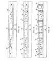
- FIGS. 3 a - 3 jillustrate a process of forming TMVs and TSVs in a WLCSP in the same direction during the same manufacturing process using the same carrier.
- a sacrificial or temporary substrate or carrier 120contains base material such as silicon, polymer, polymer composite, metal, ceramic, glass, glass epoxy, beryllium oxide, tape, or other suitable low-cost, rigid material for structural support.
- An optional interface layer 122can be formed over carrier 120 as a temporary double-sided adhesive tape or bonding film or etch-stop layer.
- semiconductor die or components 124are mounted to carrier 120 with contact pads 126 oriented downward over the carrier.
- Semiconductor die 124has an active region 128 containing analog or digital circuits implemented as active devices, passive devices, conductive layers, and dielectric layers formed within the die and electrically interconnected according to the electrical design and function of the die.
- the circuitmay include one or more transistors, diodes, and other circuit elements formed within active surface 128 to implement analog circuits or digital circuits, such as digital signal processor (DSP), ASIC, memory, or other signal processing circuit.
- DSPdigital signal processor
- Semiconductor die 124may also contain IPD, such as inductors, capacitors, and resistors, for RF signal processing.
- IPDsuch as inductors, capacitors, and resistors, for RF signal processing.
- Semiconductor die 124can be a flipchip type device or wire bond type device. In another embodiment, a discrete component can be mounted over interface layer 122 and carrier 120 .
- FIG. 3 cshows an encapsulant or molding compound 130 deposited over semiconductor die 124 and carrier 120 using a paste printing, compressive molding, transfer molding, liquid encapsulant molding, vacuum lamination, or other suitable applicator.
- Encapsulant 130can be polymer composite material, such as epoxy resin with filler, epoxy acrylate with filler, or polymer with proper filler.
- Encapsulant 130is non-conductive and environmentally protects the semiconductor device from external elements and contaminants.
- Encapsulant 130is planarized to expose back surface 132 of semiconductor die 124 , opposite active surface 128 .
- an insulating or passivation layer 134is formed over back surface 132 of semiconductor die 124 and encapsulant 130 using PVD, CVD, printing, spin coating, spray coating, or thermal oxidation process.
- the insulating layer 134can be one or more layers of silicon dioxide (SiO2), silicon nitride (Si3N4), silicon oxynitride (SiON), tantalum pentoxide (Ta2O5), aluminum oxide (Al2O3), or other material having similar insulating and structural properties.
- a plurality of vias 136is formed through insulating layer 134 and semiconductor die 124 , while the die is mounted to carrier 120 , using laser drilling, mechanical drilling, or deep reactive ion etching (DRIE) process.
- the vias 136are formed from insulating layer 134 and backside 132 , after depositing encapsulant 130 , with active surface 128 of semiconductor die 124 facing down.
- the vias 136extend through the silicon region of semiconductor die 124 to contact pads 126 .
- a plurality of vias 138is formed through insulating layer 134 and encapsulant 130 , while semiconductor die 124 is mounted to carrier 120 , using laser drilling, mechanical drilling, or DRIE.
- the vias 138are formed from the same side as vias 136 and extend to interface layer 122 .
- the vias 136 and 138are formed simultaneously or consecutively from the same side during the same manufacturing process using the same carrier 120 .
- An optional insulating or dielectric layer 140can be formed on the sidewalls of vias 136 and 138 using PVD, CVD, or thermal oxidation process.
- the insulating layer 140can be one or more layers of SiO2, Si3N4, SiON, Ta2O5, Al2O3, polyimide, benzocyclobutene (BCE), polybenzoxazoles (PBO), or other suitable dielectric material. The remaining description continues without optional insulating layer 140 .
- An electrically conductive layer 146is formed over insulating layer 134 , TMVs 142 , and TSVs 144 using patterning and PVD, CVD, electrolytic plating, electroless plating process, or other suitable metal deposition process.
- Conductive layer 146can be one or more layers of Al, Cu, Sn, Ni, Au, Ag, or other suitable electrically conductive material.
- the individual portions of conductive layer 146are electrically connected to TMVs 142 and TSVs 144 and operate as a redistribution layer (RDL) to extend the electrical connectivity for the TMVs and TSVs.
- RDLredistribution layer
- a photoresist layer 148is deposited and patterned over insulating layer 134 and conductive layer 146 . A portion of photoresist layer 148 is removed to expose conductive layer 146 .
- An optional conductive layer 147is formed over conductive layer 146 using patterning and PVD, CVD, electrolytic plating, electroless plating process, or other suitable metal deposition process.
- Conductive layer 147can be one or more layers of Al, Cu, Sn, Ni, Au, Ag, or other suitable electrically conductive material.
- Conductive layer 147forms a multi-layer under bump metallization (UBM) including a barrier layer and adhesion layer.
- UBMunder bump metallization
- the barrier layercontains Ni, titanium tungsten (TiW), chromium copper (CrCu), nickel vanadium (NiV), platinum (Pt), or palladium (Pd).
- the adhesion layercontains Al, titanium (Ti), chromium (Cr), or titanium nitride (TiN).
- UBM 147provides a low resistive interconnect, as well as a barrier to Cu or solder diffusion. Alternatively, wire-bondable pads may also be formed over conductive layer 146 . Conductive layer 146 , photoresist layer 148 , and UBM 147 constitute a build-up interconnect structure 149 .
- the build-up interconnect structure 150further includes an electrically conductive layer 156 formed over insulating layer 152 and conductive layer 154 using patterning and PVD, CVD, electrolytic plating, electroless plating process, or other suitable metal deposition process.
- Conductive layer 156can be one or more layers of Al, Cu, Sn, Ni, Au, Ag, or other suitable electrically conductive material.
- the individual portions of conductive layer 156are electrically connected to TMVs 142 and TSVs 144 and operate as an RDL to extend the electrical connectivity for the TMVs and TSVs.
- An insulating or passivation layer 158is formed over insulating layer 152 and conductive layer 156 by PVD, CVD, printing, spin coating, spray coating, or thermal oxidation.
- the insulating layer 158can be one or more layers of SiO2, Si3N4, SiON, Ta2O5, Al2O3, or other material having similar insulating and structural properties. A portion of insulating layer 158 is removed by an etching process to expose conductive layer 156 .
- An electrically conductive bump materialis deposited over conductive layer 156 using an evaporation, electrolytic plating, electroless plating, ball drop, or screen printing process.
- the bump materialcan be Al, Sn, Ni, Au, Ag, Pb, Bi, Cu, solder, and combinations thereof, with an optional flux solution.
- the bump materialcan be eutectic Sn/Pb, high-lead solder, or lead-free solder.
- the bump materialis bonded to conductive layer 156 using a suitable attachment or bonding process. In one embodiment, the bump material is ref lowed by heating the material above its melting point to form spherical balls or bumps 160 .
- bumps 160are ref lowed a second time to improve electrical contact to conductive layer 156 .
- the bumpscan also be compression bonded to conductive layer 156 .
- Bumps 160represent one type of interconnect structure that can be formed over conductive layer 156 .
- the interconnect structurecan also use bond wires, conductive paste, stud bump, micro bump, or other electrical interconnect.
- FIG. 4shows WLCSP 164 after singulation.
- Build-up interconnect structure 149is electrically connected to contact pads 126 of semiconductor die 124 and conductive layers 154 and 156 of build-up interconnect structure 150 through conductive TMVs 142 and TSVs 144 .
- TMVs 142 and TSVs 144are formed from the same side during the same manufacturing process after depositing encapsulant 130 . Since TSV 144 is formed after encapsulation, the same carrier 120 is used to form both TMVs 142 and TSVs 144 . The separate manufacturing processes and different carriers noted in the background are no longer necessary.
- TSVs 144In addition, the formation of vias in the passivation layer over the TSVs mandated in the prior art can be avoided.
- the vias 136 used to form TSVs 144extend through passivation layer 134 , thus saving a process step required in the prior art.
- the continuous structure of TMVs 142 and TSVs 144reduces contact resistance, increases conductivity, and improves signal integrity. Accordingly, forming TMVs 142 and TSV 144 from the same side during the same manufacturing process using the same carrier 120 simplifies the manufacturing, reduces cost, and reduces risk of defects.
- the formation of TSVs 144 after mounting semiconductor die 124 to carrier 120 and after depositing encapsulant 130reduces device failures due to TSV formation defects in the wafer level.
- FIG. 5shows an embodiment similar to FIG. 4 with TSVs 144 electrically connected to circuit nodes within active surface 128 to provide additional vertical (z-direction) interconnect to increase input/output (I/O) count and density to upper stacked semiconductor devices.
- TSVs 144are also electrically connected to portions of conductive layer 154 and conductive layer 156 . Other portions of conductive layer 156 and conductive layer 154 are electrically connected to contact pads 126 .
- FIG. 6shows an embodiment similar to FIG. 4 with encapsulant 130 covering back surface 132 of semiconductor die 124 .
- the insulating layer 134 described in FIG. 3 dcan be omitted as encapsulant 130 provides electrical and structural isolation.
- a photoresist or insulating layer 170is deposited and patterned over insulating layer 134 and conductive layer 168 .
- Photoresist 170fills the remaining area of vias 136 and 138 over conductive layer 166 .
- a portion of photoresist layer 170is removed to expose conductive layer 168 .
- An optional UBM 171is formed over conductive layer 168 .
- Conductive layer 168 , photoresist layer 170 , and UBM 171constitute a build-up interconnect structure 173 . The remainder of the process follows FIG. 3 g - 3 j.
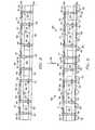
- FIG. 8shows an embodiment similar to FIG. 4 with bumps 172 formed on contact pads 126 , and contact pads 174 formed on carrier 120 , prior to mounting semiconductor die 124 to carrier 120 .
- Semiconductor die 124 with bumps 172is mounted to contact pads 174 .
- Contact pads 174are electrically connected to conductive layer 154 .
- Bumps 172provide finer interconnect pitch and increases I/O density.
- Encapsulant 130underfills semiconductor die 124 .
- FIG. 9shows an embodiment similar to FIG. 8 with TSVs 144 electrically connected to circuit nodes within active surface 128 to provide additional vertical (z-direction) interconnect to increase I/O count and density to upper stacked semiconductor devices.
- TSVs 144extend through encapsulant 130 to electrically connect to portions of conductive layer 154 and conductive layer 156 . Other portions of conductive layer 156 and conductive layer 154 are electrically connected to bumps 172 and contact pads 126 and 174 .
- FIG. 10shows an embodiment similar to FIG. 9 with an underfill material 176 , such as epoxy resin, deposited under semiconductor die 124 .
- TSVs 144are electrically connected to circuit nodes within active surface 128 to provide additional vertical (z-direction) interconnect to increase I/O count and density to upper stacked semiconductor devices.
- TSVs 144extend through underfill material 176 to electrically connect to portions of conductive layer 154 and conductive layer 156 . Other portions of conductive layer 156 and conductive layer 154 are electrically connected to contact pads 126 .
- FIG. 11shows an embodiment continuing from FIG. 3 c with carrier 120 and interface layer 122 removed by chemical etching, mechanical peel-off, CMP, mechanical grinding, thermal bake, laser scanning, or wet stripping.
- a build-up interconnect structure 180is formed over active surface 128 and encapsulant 130 .
- the build-up interconnect structure 180includes an insulating or passivation layer 182 formed by PVD, CVD, printing, spin coating, spray coating, or thermal oxidation.
- the insulating layer 182can be one or more layers of SiO2, Si3N4, SiON, Ta2O5, Al2O3, or other material having similar insulating and structural properties.
- a portion of insulating layer 182is removed by an etching process to expose contact pads 126 .
- An electrically conductive layer 184is formed in the removed portion of insulating layer 182 using patterning and PVD, CVD, electrolytic plating, electroless plating process, or other suitable metal deposition process.
- Conductive layer 184can be one or more layers of Al, Cu, Sn, Ni, Au, Ag, or other suitable electrically conductive material.
- Conductive layer 184is electrically connected to contact pads 126 .
- An electrically conductive layer 186is formed over insulating layer 182 using patterning and PVD, CVD, electrolytic plating, electroless plating process, or other suitable metal deposition process.
- Conductive layer 186can be one or more layers of Al, Cu, Sn, Ni, Au, Ag, or other suitable electrically conductive material. The individual portions of conductive layer 186 operate as an RDL to extend the electrical connectivity.
- the insulating layer 188can be one or more layers of SiO2, Si3N4, SiON, Ta2O5, Al2O3, or other material having similar insulating and structural properties. A portion of insulating layer 188 is removed by an etching process to expose conductive layer 186 .
- An electrically conductive bump materialis deposited over conductive layer 186 using an evaporation, electrolytic plating, electroless plating, ball drop, or screen printing process.
- the bump materialcan be Al, Sn, Ni, Au, Ag, Pb, Bi, Cu, solder, and combinations thereof, with an optional flux solution.
- the bump materialcan be eutectic Sn/Pb, high-lead solder, or lead-free solder.
- the bump materialis bonded to conductive layer 186 using a suitable attachment or bonding process. In one embodiment, the bump material is ref lowed by heating the material above its melting point to form spherical balls or bumps 190 .
- bumps 190are ref lowed a second time to improve electrical contact to conductive layer 186 .
- the bumpscan also be compression bonded to conductive layer 186 .
- Bumps 190represent one type of interconnect structure that can be formed over conductive layer 186 .
- the interconnect structurecan also use bond wires, conductive paste, stud bump, micro bump, or other electrical interconnect.
- An insulating or passivation layer 191is formed over back surface 132 of semiconductor die 124 and encapsulant 130 using PVD, CVD, printing, spin coating, spray coating, or thermal oxidation process.
- the insulating layer 191can be one or more layers of SiO2, Si3N4, SiON, Ta2O5, Al2O3, or other material having similar insulating and structural properties.
- a plurality of viasis formed through insulating layer 191 and semiconductor die 124 and insulating layer 182 using laser drilling, mechanical drilling, or DRIE, similar to FIG. 3 e .
- the viasare formed after depositing encapsulant 130 with active surface 128 of semiconductor die 124 facing down.
- the viasextend through insulating layer 191 and the silicon region of semiconductor die 124 and insulating layer 182 to conductive layer 186 .
- a plurality of viasis formed through insulating layer 191 and encapsulant 130 and insulating layer 182 using laser drilling, mechanical drilling, or DRIE, similar to FIG. 3 f .
- the viasare formed from the same side and extend to conductive layer 186 .
- the viasare formed simultaneously or consecutively from the same side during the same manufacturing process using the same carrier 120 .
- An optional insulating or dielectric layercan be formed on the sidewalls of the vias using PVD, CVD, or thermal oxidation process.
- the insulating layercan be one or more layers of SiO2, Si3N4, SiON, Ta2O5, Al2O3, polyimide, BCB, PBO, or other suitable dielectric material.
- the vias through encapsulant 130are filled with Al, Cu, Sn, Ni, Au, Ag, Ti, W, poly-silicon, or other suitable electrically conductive material using electrolytic plating, electroless plating process, or other suitable metal deposition process to form conductive TMVs 192 .
- TMVs 192are electrically connected to portions of conductive layer 186 .
- the vias through semiconductor die 124are filled with Al, Cu, Sn, Ni, Au, Ag, Ti, W, poly-silicon, or other suitable electrically conductive material using electrolytic plating, electroless plating process, or other suitable metal deposition process to form conductive TSVs 194 .
- TSVs 194are electrically connected to other portions of conductive layer 186 .
- An electrically conductive layer 196is formed over insulating layer 191 , TMVs 192 , and TSVs 194 using patterning and PVD, CVD, electrolytic plating, electroless plating process, or other suitable metal deposition process.
- Conductive layer 196can be one or more layers of Al, Cu, Sn, Ni, Au, Ag, or other suitable electrically conductive material.
- Conductive layer 196is electrically connected to TMVs 192 and TSVs 194 and operates as an RDL to extend the electrical connectivity for the TMVs and TSVs.
- UBM 200provides a low resistive interconnect, as well as a barrier to Cu or solder diffusion. Alternatively, wire-bondable pads may also be formed over conductive layer 196 . Conductive layer 196 , photoresist layer 198 , and UBM 200 constitute a build-up interconnect structure 202 .
- build-up interconnect structure 202is electrically connected to contact pads 126 of semiconductor die 124 and conductive layers 184 and 186 of build-up interconnect structure 180 through conductive TMVs 192 and TSVs 194 .
- TMVs 192 and TSVs 194are formed from the same side during the same manufacturing process after depositing encapsulant 130 . Since TSV 194 is formed after encapsulation, the same support structure, i.e., build-up interconnect structure 180 , is used to form both TMVs 192 and TSVs 194 .
- the separate manufacturing processes and different carriers noted in the backgroundare no longer necessary.
- the formation of vias in the passivation layer over TSVs mandated in the prior artcan be avoided.
- TSVs 194extend through passivation layer 191 , thus saving a process step required in the prior art.
- the continuous structure of TMVs 192 and TSVs 194reduces contact resistance, increases conductivity, and improves signal integrity. Accordingly, forming TMVs 192 and TSV 194 from the same side during the same manufacturing process using the same support structure simplifies the manufacturing, reduces cost, and reduces risk of defects.
- the formation of TSVs 194 after mounting semiconductor die 124 to carrier 120 and after depositing encapsulant 130reduces device failures due to TSV formation defects in the wafer level.
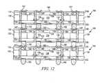
- FIG. 12shows stacked WLCSP 164 from FIG. 4 electrically interconnected in the z-direction by conductive layer 146 , UBM 147 , TMVs 142 , TSVs 144 , bumps 160 , and conductive layers 154 and 156 of build-up interconnect structure 150 .
Landscapes
- Engineering & Computer Science (AREA)
- Microelectronics & Electronic Packaging (AREA)
- Power Engineering (AREA)
- Computer Hardware Design (AREA)
- Physics & Mathematics (AREA)
- Condensed Matter Physics & Semiconductors (AREA)
- General Physics & Mathematics (AREA)
- Manufacturing & Machinery (AREA)
- Internal Circuitry In Semiconductor Integrated Circuit Devices (AREA)
- Semiconductor Integrated Circuits (AREA)
Abstract
Description
- The present invention relates in general to semiconductor devices and, more particularly, to a semiconductor device and method of forming TMVs and TSVs in a WLCSP in the same direction during the same manufacturing process using the same carrier.
- Semiconductor devices are commonly found in modern electronic products. Semiconductor devices vary in the number and density of electrical components. Discrete semiconductor devices generally contain one type of electrical component, e.g., light emitting diode (LED), small signal transistor, resistor, capacitor, inductor, and power metal oxide semiconductor field effect transistor (MOSFET). Integrated semiconductor devices typically contain hundreds to millions of electrical components. Examples of integrated semiconductor devices include microcontrollers, microprocessors, charged-coupled devices (CCDs), solar cells, and digital micro-mirror devices (DMDs).
- Semiconductor devices perform a wide range of functions such as high-speed calculations, transmitting and receiving electromagnetic signals, controlling electronic devices, transforming sunlight to electricity, and creating visual projections for television displays. Semiconductor devices are found in the fields of entertainment, communications, power conversion, networks, computers, and consumer products. Semiconductor devices are also found in military applications, aviation, automotive, industrial controllers, and office equipment.
- Semiconductor devices exploit the electrical properties of semiconductor materials. The atomic structure of semiconductor material allows its electrical conductivity to be manipulated by the application of an electric field or base current or through the process of doping. Doping introduces impurities into the semiconductor material to manipulate and control the conductivity of the semiconductor device.
- A semiconductor device contains active and passive electrical structures. Active structures, including bipolar and field effect transistors, control the flow of electrical current. By varying levels of doping and application of an electric field or base current, the transistor either promotes or restricts the flow of electrical current. Passive structures, including resistors, capacitors, and inductors, create a relationship between voltage and current necessary to perform a variety of electrical functions. The passive and active structures are electrically connected to form circuits, which enable the semiconductor device to perform high-speed calculations and other useful functions.
- Semiconductor devices are generally manufactured using two complex manufacturing processes, i.e., front-end manufacturing, and back-end manufacturing, each involving potentially hundreds of steps. Front-end manufacturing involves the formation of a plurality of die on the surface of a semiconductor wafer. Each die is typically identical and contains circuits formed by electrically connecting active and passive components. Back-end manufacturing involves singulating individual die from the finished wafer and packaging the die to provide structural support and environmental isolation.
- One goal of semiconductor manufacturing is to produce smaller semiconductor devices. Smaller devices typically consume less power, have higher performance, and can be produced more efficiently. In addition, smaller semiconductor devices have a smaller footprint, which is desirable for smaller end products. A smaller die size may be achieved by improvements in the front-end process resulting in die with smaller, higher density active and passive components. Back-end processes may result in semiconductor device packages with a smaller footprint by improvements in electrical interconnection and packaging materials.
- Semiconductor devices often require vertical interconnect structures, for example, when stacking devices for efficient integration. The electrical interconnection between semiconductor devices, such as fan-out wafer level chip scale package (FO-WLCSP) containing semiconductor die, on multiple levels and external devices can be accomplished with conductive through silicon vias (TSV), conductive through hole vias (THV), conductive through mold vias (TMV), Cu-plated conductive pillars, and conductive bumps. These vertical interconnect structures are costly and time consuming during the manufacturing process, and susceptible to defects during formation.
- In particular, in a WLCSP, the conductive TSV is formed first, prior to singulation while in wafer form, using a first carrier for support. The conductive TMV is formed later in the process, after encapsulation, using a different carrier for support. A build-up interconnect structure is typically formed over the semiconductor die. Additional processing steps are required to form vias in the build-up layers to reroute TSV for interconnection to the upper semiconductor device. After forming TSVs in the semiconductor die, conductive vias must be formed in the passivation layer over the TSVs to electrically connect the TSVs to upper conductive layers. Since the TSV and TMV are formed by separate processes on different carriers, the manufacturing process requires more time, material, and steps, which adds cost and greater risk of introducing defects in the semiconductor device or the entire wafer. For example, since the TSV are formed while in wafer form, the semiconductor wafer is subject to damage.
- A need exists for a simple and cost-effective process to form TSV and TMV in a WLCSP. Accordingly, in one embodiment, the present invention is a method of manufacturing a semiconductor device comprising the steps of providing a temporary carrier, mounting a semiconductor die over the temporary carrier, depositing an encapsulant over the semiconductor die and temporary carrier, forming a first insulating layer over the semiconductor die and encapsulant, forming a plurality of first vias through the first insulating layer and semiconductor die while mounted to the temporary carrier, forming a plurality of second vias through the first insulating layer and encapsulant while the semiconductor die is mounted to the temporary carrier, depositing electrically conductive material in the first vias to form conductive TSV, depositing electrically conductive material in the second vias to form conductive TMV, forming a first interconnect structure over the first insulating layer and electrically connected to the conductive TSV and conductive TMV, removing the temporary carrier, and forming a second interconnect structure over the semiconductor die and encapsulant opposite the first interconnect structure and electrically connected to the conductive TSV and conductive TMV.
- In another embodiment, the present invention is a method of manufacturing a semiconductor device comprising the steps of providing a carrier, mounting a semiconductor die over the carrier, depositing an encapsulant over the semiconductor die and carrier, forming a plurality of first vias through the semiconductor die while mounted to the carrier, forming a plurality of second vias through the encapsulant in the same direction as the first vias, depositing electrically conductive material in the first vias to form first conductive vias and in the second vias to form second conductive vias, forming a first interconnect structure over the encapsulant and electrically connected to the first conductive vias and second conductive vias, removing the carrier, and forming a second interconnect structure over the encapsulant opposite the first interconnect structure and electrically connected to the first conductive and second conductive vias.
- In another embodiment, the present invention is a method of manufacturing a semiconductor device comprising the steps of providing a carrier, mounting a semiconductor die over the carrier with an active surface of the semiconductor die oriented toward the carrier, depositing an encapsulant over the semiconductor die and carrier, removing the carrier, forming a first interconnect structure over the encapsulant and active surface of the semiconductor die, forming a plurality of first vias through the semiconductor die and a portion of the first interconnect structure, forming a plurality of second vias through the encapsulant and a portion of the first interconnect structure in the same direction as the first vias, depositing electrically conductive material in the first vias to form first conductive vias and in the second vias to form second conductive vias, and forming a second interconnect structure over the encapsulant opposite the first interconnect structure and electrically connected to the first conductive vias and second conductive vias.
- In another embodiment, the present invention is a semiconductor device comprising a semiconductor die and encapsulant deposited over the semiconductor die. A first conductive via is formed through the semiconductor die. A second conductive via is formed through the encapsulant in the same direction as the first conductive via. A first interconnect structure is formed over the encapsulant and electrically connected to the first conductive via and second conductive via. A second interconnect structure is formed over the encapsulant opposite the first interconnect structure and electrically connected to the first conductive via and second conductive via.
FIG. 1 illustrates a PCB with different types of packages mounted to its surface;FIGS. 2 a-2cillustrate further detail of the semiconductor packages mounted to the PCB;FIGS. 3 a-3jillustrate a process of forming TMVs and TSVs in a WLCSP in the same direction during the same manufacturing process using the same carrier;FIG. 4 illustrates the stackable WLCSP with TMVs and TSVs;FIG. 5 illustrates the TSVs electrically connected to the active surface of the die;FIG. 6 illustrates the encapsulant covering the back surface of the semiconductor die;FIG. 7 illustrates the TMVs and TSVs conformally formed in the vias and then filled with photoresist material;FIG. 8 illustrates bumped semiconductor die mounted to contact pads on the carrier;FIG. 9 illustrates bumped semiconductor die mounted to contact pads on the carrier and the TSVs electrically connected to the active surface of the die;FIG. 10 illustrates bumped semiconductor die mounted to contact pads on the carrier with underfill material;FIG. 11 illustrates using the lower build-up interconnect structure as support to form the TMVs and TSVs during the same manufacturing process in the same direction; andFIG. 12 illustrates stacked WLCSP interconnected by the TMVs, TSVs, and interconnect structures.- The present invention is described in one or more embodiments in the following description with reference to the figures, in which like numerals represent the same or similar elements. While the invention is described in terms of the best mode for achieving the invention's objectives, it will be appreciated by those skilled in the art that it is intended to cover alternatives, modifications, and equivalents as may be included within the spirit and scope of the invention as defined by the appended claims and their equivalents as supported by the following disclosure and drawings.
- Semiconductor devices are generally manufactured using two complex manufacturing processes: front-end manufacturing and back-end manufacturing. Front-end manufacturing involves the formation of a plurality of die on the surface of a semiconductor wafer. Each die on the wafer contains active and passive electrical components, which are electrically connected to form functional electrical circuits. Active electrical components, such as transistors and diodes, have the ability to control the flow of electrical current. Passive electrical components, such as capacitors, inductors, resistors, and transformers, create a relationship between voltage and current necessary to perform electrical circuit functions.
- Passive and active components are formed over the surface of the semiconductor wafer by a series of process steps including doping, deposition, photolithography, etching, and planarization. Doping introduces impurities into the semiconductor material by techniques such as ion implantation or thermal diffusion. The doping process modifies the electrical conductivity of semiconductor material in active devices, transforming the semiconductor material into an insulator, conductor, or dynamically changing the semiconductor material conductivity in response to an electric field or base current. Transistors contain regions of varying types and degrees of doping arranged as necessary to enable the transistor to promote or restrict the flow of electrical current upon the application of the electric field or base current.
- Active and passive components are formed by layers of materials with different electrical properties. The layers can be formed by a variety of deposition techniques determined in part by the type of material being deposited. For example, thin film deposition may involve chemical vapor deposition (CVD), physical vapor deposition (PVD), electrolytic plating, and electroless plating processes. Each layer is generally patterned to form portions of active components, passive components, or electrical connections between components.
- The layers can be patterned using photolithography, which involves the deposition of light sensitive material, e.g., photoresist, over the layer to be patterned. A pattern is transferred from a photomask to the photoresist using light. The portion of the photoresist pattern subjected to light is removed using a solvent, exposing portions of the underlying layer to be patterned. The remainder of the photoresist is removed, leaving behind a patterned layer. Alternatively, some types of materials are patterned by directly depositing the material into the areas or voids formed by a previous deposition/etch process using techniques such as electroless and electrolytic plating.
- Depositing a thin film of material over an existing pattern can exaggerate the underlying pattern and create a non-uniformly flat surface. A uniformly flat surface is required to produce smaller and more densely packed active and passive components. Planarization can be used to remove material from the surface of the wafer and produce a uniformly flat surface. Planarization involves polishing the surface of the wafer with a polishing pad. An abrasive material and corrosive chemical are added to the surface of the wafer during polishing. The combined mechanical action of the abrasive and corrosive action of the chemical removes any irregular topography, resulting in a uniformly flat surface.
- Back-end manufacturing refers to cutting or singulating the finished wafer into the individual die and then packaging the die for structural support and environmental isolation. To singulate the die, the wafer is scored and broken along non-functional regions of the wafer called saw streets or scribes. The wafer is singulated using a laser cutting tool or saw blade. After singulation, the individual die are mounted to a package substrate that includes pins or contact pads for interconnection with other system components. Contact pads formed over the semiconductor die are then connected to contact pads within the package. The electrical connections can be made with solder bumps, stud bumps, conductive paste, or wirebonds. An encapsulant or other molding material is deposited over the package to provide physical support and electrical isolation. The finished package is then inserted into an electrical system and the functionality of the semiconductor device is made available to the other system components.
FIG. 1 illustrateselectronic device 50 having a chip carrier substrate or printed circuit board (PCB)52 with a plurality of semiconductor packages mounted on its surface.Electronic device 50 may have one type of semiconductor package, or multiple types of semiconductor packages, depending on the application. The different types of semiconductor packages are shown inFIG. 1 for purposes of illustration.Electronic device 50 may be a stand-alone system that uses the semiconductor packages to perform one or more electrical functions. Alternatively,electronic device 50 may be a subcomponent of a larger system. For example,electronic device 50 may be a graphics card, network interface card, or other signal processing card that can be inserted into a computer. The semiconductor package can include microprocessors, memories, application specific integrated circuits (ASIC), logic circuits, analog circuits, RF circuits, discrete devices, or other semiconductor die or electrical components.- In
FIG. 1 ,PCB 52 provides a general substrate for structural support and electrical interconnect of the semiconductor packages mounted on the PCB. Conductive signal traces54 are formed over a surface or within layers ofPCB 52 using evaporation, electrolytic plating, electroless plating, screen printing, or other suitable metal deposition process. Signal traces54 provide for electrical communication between each of the semiconductor packages, mounted components, and other external system components.Traces 54 also provide power and ground connections to each of the semiconductor packages. - In some embodiments, a semiconductor device has two packaging levels. First level packaging is a technique for mechanically and electrically attaching the semiconductor die to an intermediate carrier. Second level packaging involves mechanically and electrically attaching the intermediate carrier to the PCB. In other embodiments, a semiconductor device may only have the first level packaging where the die is mechanically and electrically mounted directly to the PCB.
- For the purpose of illustration, several types of first level packaging, including
wire bond package 56 andflip chip 58, are shown onPCB 52. Additionally, several types of second level packaging, including ball grid array (BGA)60, bump chip carrier (BCC)62, dual in-line package (DIP)64, land grid array (LGA)66, multi-chip module (MCM)68, quad flat non-leaded package (QFN)70, and quadflat package 72, are shown mounted onPCB 52. Depending upon the system requirements, any combination of semiconductor packages, configured with any combination of first and second level packaging styles, as well as other electronic components, can be connected toPCB 52. In some embodiments,electronic device 50 includes a single attached semiconductor package, while other embodiments call for multiple interconnected packages. By combining one or more semiconductor packages over a single substrate, manufacturers can incorporate pre-made components into electronic devices and systems. Because the semiconductor packages include sophisticated functionality, electronic devices can be manufactured using cheaper components and a streamlined manufacturing process. The resulting devices are less likely to fail and less expensive to manufacture resulting in a lower cost for consumers. FIGS. 2 a-2cshow exemplary semiconductor packages.FIG. 2 aillustrates further detail ofDIP 64 mounted onPCB 52. Semiconductor die74 includes an active region containing analog or digital circuits implemented as active devices, passive devices, conductive layers, and dielectric layers formed within the die and are electrically interconnected according to the electrical design of the die. For example, the circuit may include one or more transistors, diodes, inductors, capacitors, resistors, and other circuit elements formed within the active region of semiconductor die74. Contactpads 76 are one or more layers of conductive material, such as aluminum (Al), copper (Cu), tin (Sn), nickel (Ni), gold (Au), or silver (Ag), and are electrically connected to the circuit elements formed within semiconductor die74. During assembly ofDIP 64, semiconductor die74 is mounted to anintermediate carrier 78 using a gold-silicon eutectic layer or adhesive material such as thermal epoxy or epoxy resin. The package body includes an insulative packaging material such as polymer or ceramic. Conductor leads80 andwire bonds 82 provide electrical interconnect between semiconductor die74 andPCB 52.Encapsulant 84 is deposited over the package for environmental protection by preventing moisture and particles from entering the package and contaminating die74 or wire bonds82.FIG. 2 billustrates further detail ofBCC 62 mounted onPCB 52. Semiconductor die88 is mounted overcarrier 90 using an underfill or epoxy-resin adhesive material 92.Wire bonds 94 provide first level packaging interconnect betweencontact pads encapsulant 100 is deposited over semiconductor die88 andwire bonds 94 to provide physical support and electrical isolation for the device. Contactpads 102 are formed over a surface ofPCB 52 using a suitable metal deposition process such as electrolytic plating or electroless plating to prevent oxidation. Contactpads 102 are electrically connected to one or more conductive signal traces54 inPCB 52.Bumps 104 are formed betweencontact pads 98 ofBCC 62 andcontact pads 102 ofPCB 52.- In
FIG. 2 c, semiconductor die58 is mounted face down tointermediate carrier 106 with a flip chip style first level packaging.Active region 108 of semiconductor die58 contains analog or digital circuits implemented as active devices, passive devices, conductive layers, and dielectric layers formed according to the electrical design of the die. For example, the circuit may include one or more transistors, diodes, inductors, capacitors, resistors, and other circuit elements withinactive region 108. Semiconductor die58 is electrically and mechanically connected tocarrier 106 throughbumps 110. BGA 60 is electrically and mechanically connected toPCB 52 with a BGA style second levelpackaging using bumps 112. Semiconductor die58 is electrically connected to conductive signal traces54 inPCB 52 throughbumps 110,signal lines 114, and bumps112. A molding compound orencapsulant 116 is deposited over semiconductor die58 andcarrier 106 to provide physical support and electrical isolation for the device. The flip chip semiconductor device provides a short electrical conduction path from the active devices on semiconductor die58 to conduction tracks onPCB 52 in order to reduce signal propagation distance, lower capacitance, and improve overall circuit performance. In another embodiment, the semiconductor die58 can be mechanically and electrically connected directly toPCB 52 using flip chip style first level packaging withoutintermediate carrier 106.FIGS. 3 a-3jillustrate a process of forming TMVs and TSVs in a WLCSP in the same direction during the same manufacturing process using the same carrier. InFIG. 3 a, a sacrificial or temporary substrate orcarrier 120 contains base material such as silicon, polymer, polymer composite, metal, ceramic, glass, glass epoxy, beryllium oxide, tape, or other suitable low-cost, rigid material for structural support. Anoptional interface layer 122 can be formed overcarrier 120 as a temporary double-sided adhesive tape or bonding film or etch-stop layer.- In
FIG. 3 b, semiconductor die orcomponents 124 are mounted tocarrier 120 withcontact pads 126 oriented downward over the carrier. Semiconductor die124 has anactive region 128 containing analog or digital circuits implemented as active devices, passive devices, conductive layers, and dielectric layers formed within the die and electrically interconnected according to the electrical design and function of the die. For example, the circuit may include one or more transistors, diodes, and other circuit elements formed withinactive surface 128 to implement analog circuits or digital circuits, such as digital signal processor (DSP), ASIC, memory, or other signal processing circuit. Semiconductor die124 may also contain IPD, such as inductors, capacitors, and resistors, for RF signal processing. Semiconductor die124 can be a flipchip type device or wire bond type device. In another embodiment, a discrete component can be mounted overinterface layer 122 andcarrier 120. FIG. 3 cshows an encapsulant ormolding compound 130 deposited over semiconductor die124 andcarrier 120 using a paste printing, compressive molding, transfer molding, liquid encapsulant molding, vacuum lamination, or other suitable applicator.Encapsulant 130 can be polymer composite material, such as epoxy resin with filler, epoxy acrylate with filler, or polymer with proper filler.Encapsulant 130 is non-conductive and environmentally protects the semiconductor device from external elements and contaminants.Encapsulant 130 is planarized to expose backsurface 132 of semiconductor die124, oppositeactive surface 128.- In
FIG. 3 d, an insulating orpassivation layer 134 is formed overback surface 132 of semiconductor die124 andencapsulant 130 using PVD, CVD, printing, spin coating, spray coating, or thermal oxidation process. The insulatinglayer 134 can be one or more layers of silicon dioxide (SiO2), silicon nitride (Si3N4), silicon oxynitride (SiON), tantalum pentoxide (Ta2O5), aluminum oxide (Al2O3), or other material having similar insulating and structural properties. - In
FIG. 3 e, a plurality ofvias 136 is formed through insulatinglayer 134 and semiconductor die124, while the die is mounted tocarrier 120, using laser drilling, mechanical drilling, or deep reactive ion etching (DRIE) process. Thevias 136 are formed from insulatinglayer 134 andbackside 132, after depositingencapsulant 130, withactive surface 128 of semiconductor die124 facing down. Thevias 136 extend through the silicon region of semiconductor die124 to contactpads 126. Likewise, inFIG. 3 f, a plurality ofvias 138 is formed through insulatinglayer 134 andencapsulant 130, while semiconductor die124 is mounted tocarrier 120, using laser drilling, mechanical drilling, or DRIE. Thevias 138 are formed from the same side asvias 136 and extend to interfacelayer 122. Thevias same carrier 120. - An optional insulating or
dielectric layer 140 can be formed on the sidewalls ofvias layer 140 can be one or more layers of SiO2, Si3N4, SiON, Ta2O5, Al2O3, polyimide, benzocyclobutene (BCE), polybenzoxazoles (PBO), or other suitable dielectric material. The remaining description continues without optional insulatinglayer 140. - In
FIG. 3 g, thevias 138 are filled with Al, Cu, Sn, Ni, Au, Ag, titanium (Ti), W, poly-silicon, or other suitable electrically conductive material using electrolytic plating, electroless plating process, or other suitable metal deposition process to form conductive through mold vias (TMV)142. Thevias 136 are filled with Al, Cu, Sn, Ni, Au, Ag, Ti, W, poly-silicon, or other suitable electrically conductive material using electrolytic plating, electroless plating process, or other suitable metal deposition process to form conductive through silicon vias (TSV)144.TSVs 144 are electrically connected to contactpads 126. - An electrically
conductive layer 146 is formed overinsulating layer 134,TMVs 142, andTSVs 144 using patterning and PVD, CVD, electrolytic plating, electroless plating process, or other suitable metal deposition process.Conductive layer 146 can be one or more layers of Al, Cu, Sn, Ni, Au, Ag, or other suitable electrically conductive material. The individual portions ofconductive layer 146 are electrically connected to TMVs142 andTSVs 144 and operate as a redistribution layer (RDL) to extend the electrical connectivity for the TMVs and TSVs. - In
FIG. 3 h, aphotoresist layer 148 is deposited and patterned overinsulating layer 134 andconductive layer 146. A portion ofphotoresist layer 148 is removed to exposeconductive layer 146. An optionalconductive layer 147 is formed overconductive layer 146 using patterning and PVD, CVD, electrolytic plating, electroless plating process, or other suitable metal deposition process.Conductive layer 147 can be one or more layers of Al, Cu, Sn, Ni, Au, Ag, or other suitable electrically conductive material.Conductive layer 147 forms a multi-layer under bump metallization (UBM) including a barrier layer and adhesion layer. In one embodiment, the barrier layer contains Ni, titanium tungsten (TiW), chromium copper (CrCu), nickel vanadium (NiV), platinum (Pt), or palladium (Pd). The adhesion layer contains Al, titanium (Ti), chromium (Cr), or titanium nitride (TiN).UBM 147 provides a low resistive interconnect, as well as a barrier to Cu or solder diffusion. Alternatively, wire-bondable pads may also be formed overconductive layer 146.Conductive layer 146,photoresist layer 148, andUBM 147 constitute a build-upinterconnect structure 149. - In
FIG. 3 i,carrier 120 andinterface layer 122 are removed by chemical etching, mechanical peel-off, CMP, mechanical grinding, thermal bake, laser scanning, or wet stripping. A build-upinterconnect structure 150 is formed overactive surface 128 andencapsulant 130. The build-upinterconnect structure 150 includes an insulating orpassivation layer 152 formed by PVD, CVD, printing, spin coating, spray coating, or thermal oxidation. The insulatinglayer 152 can be one or more layers of SiO2, Si3N4, SiON, Ta2O5, Al2O3, or other material having similar insulating and structural properties. A portion of insulatinglayer 152 is removed by an etching process to exposeTMVs 142 andTSVs 144. An electricallyconductive layer 154 is formed in the removed portion of insulatinglayer 152 using patterning and PVD, CVD, electrolytic plating, electroless plating process, or other suitable metal deposition process.Conductive layer 154 can be one or more layers of Al, Cu, Sn, Ni, Au, Ag, or other suitable electrically conductive material. The individual portions ofconductive layer 154 are electrically connected to TMVs142 andTSVs 144. - In
FIG. 3 j, the build-upinterconnect structure 150 further includes an electricallyconductive layer 156 formed overinsulating layer 152 andconductive layer 154 using patterning and PVD, CVD, electrolytic plating, electroless plating process, or other suitable metal deposition process.Conductive layer 156 can be one or more layers of Al, Cu, Sn, Ni, Au, Ag, or other suitable electrically conductive material. The individual portions ofconductive layer 156 are electrically connected to TMVs142 andTSVs 144 and operate as an RDL to extend the electrical connectivity for the TMVs and TSVs. - An insulating or
passivation layer 158 is formed overinsulating layer 152 andconductive layer 156 by PVD, CVD, printing, spin coating, spray coating, or thermal oxidation. The insulatinglayer 158 can be one or more layers of SiO2, Si3N4, SiON, Ta2O5, Al2O3, or other material having similar insulating and structural properties. A portion of insulatinglayer 158 is removed by an etching process to exposeconductive layer 156. - An electrically conductive bump material is deposited over
conductive layer 156 using an evaporation, electrolytic plating, electroless plating, ball drop, or screen printing process. The bump material can be Al, Sn, Ni, Au, Ag, Pb, Bi, Cu, solder, and combinations thereof, with an optional flux solution. For example, the bump material can be eutectic Sn/Pb, high-lead solder, or lead-free solder. The bump material is bonded toconductive layer 156 using a suitable attachment or bonding process. In one embodiment, the bump material is ref lowed by heating the material above its melting point to form spherical balls or bumps160. In some applications, bumps160 are ref lowed a second time to improve electrical contact toconductive layer 156. The bumps can also be compression bonded toconductive layer 156.Bumps 160 represent one type of interconnect structure that can be formed overconductive layer 156. The interconnect structure can also use bond wires, conductive paste, stud bump, micro bump, or other electrical interconnect. - Semiconductor die124 are singulated with saw blade or
laser cutting device 162 into individualstackable WLCSP 164.FIG. 4 showsWLCSP 164 after singulation. Build-upinterconnect structure 149 is electrically connected to contactpads 126 of semiconductor die124 andconductive layers interconnect structure 150 throughconductive TMVs 142 andTSVs 144.TMVs 142 andTSVs 144 are formed from the same side during the same manufacturing process after depositingencapsulant 130. SinceTSV 144 is formed after encapsulation, thesame carrier 120 is used to form bothTMVs 142 andTSVs 144. The separate manufacturing processes and different carriers noted in the background are no longer necessary. In addition, the formation of vias in the passivation layer over the TSVs mandated in the prior art can be avoided. Thevias 136 used to formTSVs 144 extend throughpassivation layer 134, thus saving a process step required in the prior art. The continuous structure ofTMVs 142 andTSVs 144 reduces contact resistance, increases conductivity, and improves signal integrity. Accordingly, formingTMVs 142 andTSV 144 from the same side during the same manufacturing process using thesame carrier 120 simplifies the manufacturing, reduces cost, and reduces risk of defects. The formation ofTSVs 144 after mounting semiconductor die124 tocarrier 120 and after depositingencapsulant 130 reduces device failures due to TSV formation defects in the wafer level. FIG. 5 shows an embodiment similar toFIG. 4 withTSVs 144 electrically connected to circuit nodes withinactive surface 128 to provide additional vertical (z-direction) interconnect to increase input/output (I/O) count and density to upper stacked semiconductor devices.TSVs 144 are also electrically connected to portions ofconductive layer 154 andconductive layer 156. Other portions ofconductive layer 156 andconductive layer 154 are electrically connected to contactpads 126.FIG. 6 shows an embodiment similar toFIG. 4 withencapsulant 130 covering backsurface 132 of semiconductor die124. The insulatinglayer 134 described inFIG. 3 dcan be omitted asencapsulant 130 provides electrical and structural isolation.FIG. 7 shows an embodiment continuing fromFIG. 3 fwithconductive layer 166 conformally formed on the sidewalls ofvias Conductive layer 166 can be one or more layers of Al, Cu, Sn, Ni, Au, Ag, or other suitable electrically conductive material.- An electrically
conductive layer 168 is formed overinsulating layer 134 using patterning and PVD, CVD, electrolytic plating, electroless plating process, or other suitable metal deposition process.Conductive layer 168 can be one or more layers of Al, Cu, Sn, Ni, Au, Ag, or other suitable electrically conductive material.Conductive layer 168 is electrically connected toconductive layer 166 formed invias - A photoresist or insulating
layer 170 is deposited and patterned overinsulating layer 134 andconductive layer 168.Photoresist 170 fills the remaining area ofvias conductive layer 166. A portion ofphotoresist layer 170 is removed to exposeconductive layer 168. Anoptional UBM 171 is formed overconductive layer 168.Conductive layer 168,photoresist layer 170, andUBM 171 constitute a build-upinterconnect structure 173. The remainder of the process followsFIG. 3 g-3j. FIG. 8 shows an embodiment similar toFIG. 4 withbumps 172 formed oncontact pads 126, andcontact pads 174 formed oncarrier 120, prior to mounting semiconductor die124 tocarrier 120. Semiconductor die124 withbumps 172 is mounted to contactpads 174. Contactpads 174 are electrically connected toconductive layer 154.Bumps 172 provide finer interconnect pitch and increases I/O density.Encapsulant 130 underfills semiconductor die124.FIG. 9 shows an embodiment similar toFIG. 8 withTSVs 144 electrically connected to circuit nodes withinactive surface 128 to provide additional vertical (z-direction) interconnect to increase I/O count and density to upper stacked semiconductor devices.TSVs 144 extend throughencapsulant 130 to electrically connect to portions ofconductive layer 154 andconductive layer 156. Other portions ofconductive layer 156 andconductive layer 154 are electrically connected tobumps 172 andcontact pads FIG. 10 shows an embodiment similar toFIG. 9 with anunderfill material 176, such as epoxy resin, deposited under semiconductor die124.TSVs 144 are electrically connected to circuit nodes withinactive surface 128 to provide additional vertical (z-direction) interconnect to increase I/O count and density to upper stacked semiconductor devices.TSVs 144 extend throughunderfill material 176 to electrically connect to portions ofconductive layer 154 andconductive layer 156. Other portions ofconductive layer 156 andconductive layer 154 are electrically connected to contactpads 126.FIG. 11 shows an embodiment continuing fromFIG. 3 cwithcarrier 120 andinterface layer 122 removed by chemical etching, mechanical peel-off, CMP, mechanical grinding, thermal bake, laser scanning, or wet stripping. A build-upinterconnect structure 180 is formed overactive surface 128 andencapsulant 130. The build-upinterconnect structure 180 includes an insulating orpassivation layer 182 formed by PVD, CVD, printing, spin coating, spray coating, or thermal oxidation. The insulatinglayer 182 can be one or more layers of SiO2, Si3N4, SiON, Ta2O5, Al2O3, or other material having similar insulating and structural properties. A portion of insulatinglayer 182 is removed by an etching process to exposecontact pads 126. An electricallyconductive layer 184 is formed in the removed portion of insulatinglayer 182 using patterning and PVD, CVD, electrolytic plating, electroless plating process, or other suitable metal deposition process.Conductive layer 184 can be one or more layers of Al, Cu, Sn, Ni, Au, Ag, or other suitable electrically conductive material.Conductive layer 184 is electrically connected to contactpads 126.- An electrically
conductive layer 186 is formed overinsulating layer 182 using patterning and PVD, CVD, electrolytic plating, electroless plating process, or other suitable metal deposition process.Conductive layer 186 can be one or more layers of Al, Cu, Sn, Ni, Au, Ag, or other suitable electrically conductive material. The individual portions ofconductive layer 186 operate as an RDL to extend the electrical connectivity. - An insulating or
passivation layer 188 formed overinsulating layer 182 andconductive layer 186 by PVD, CVD, printing, spin coating, spray coating, or thermal oxidation. The insulatinglayer 188 can be one or more layers of SiO2, Si3N4, SiON, Ta2O5, Al2O3, or other material having similar insulating and structural properties. A portion of insulatinglayer 188 is removed by an etching process to exposeconductive layer 186. - An electrically conductive bump material is deposited over
conductive layer 186 using an evaporation, electrolytic plating, electroless plating, ball drop, or screen printing process. The bump material can be Al, Sn, Ni, Au, Ag, Pb, Bi, Cu, solder, and combinations thereof, with an optional flux solution. For example, the bump material can be eutectic Sn/Pb, high-lead solder, or lead-free solder. The bump material is bonded toconductive layer 186 using a suitable attachment or bonding process. In one embodiment, the bump material is ref lowed by heating the material above its melting point to form spherical balls or bumps190. In some applications, bumps190 are ref lowed a second time to improve electrical contact toconductive layer 186. The bumps can also be compression bonded toconductive layer 186.Bumps 190 represent one type of interconnect structure that can be formed overconductive layer 186. The interconnect structure can also use bond wires, conductive paste, stud bump, micro bump, or other electrical interconnect. - An insulating or
passivation layer 191 is formed overback surface 132 of semiconductor die124 andencapsulant 130 using PVD, CVD, printing, spin coating, spray coating, or thermal oxidation process. The insulatinglayer 191 can be one or more layers of SiO2, Si3N4, SiON, Ta2O5, Al2O3, or other material having similar insulating and structural properties. - A plurality of vias is formed through insulating
layer 191 and semiconductor die124 and insulatinglayer 182 using laser drilling, mechanical drilling, or DRIE, similar toFIG. 3 e. The vias are formed after depositingencapsulant 130 withactive surface 128 of semiconductor die124 facing down. The vias extend through insulatinglayer 191 and the silicon region of semiconductor die124 and insulatinglayer 182 toconductive layer 186. Likewise, a plurality of vias is formed through insulatinglayer 191 andencapsulant 130 and insulatinglayer 182 using laser drilling, mechanical drilling, or DRIE, similar toFIG. 3 f. The vias are formed from the same side and extend toconductive layer 186. The vias are formed simultaneously or consecutively from the same side during the same manufacturing process using thesame carrier 120. - An optional insulating or dielectric layer can be formed on the sidewalls of the vias using PVD, CVD, or thermal oxidation process. The insulating layer can be one or more layers of SiO2, Si3N4, SiON, Ta2O5, Al2O3, polyimide, BCB, PBO, or other suitable dielectric material.
- The vias through
encapsulant 130 are filled with Al, Cu, Sn, Ni, Au, Ag, Ti, W, poly-silicon, or other suitable electrically conductive material using electrolytic plating, electroless plating process, or other suitable metal deposition process to formconductive TMVs 192.TMVs 192 are electrically connected to portions ofconductive layer 186. The vias through semiconductor die124 are filled with Al, Cu, Sn, Ni, Au, Ag, Ti, W, poly-silicon, or other suitable electrically conductive material using electrolytic plating, electroless plating process, or other suitable metal deposition process to formconductive TSVs 194.TSVs 194 are electrically connected to other portions ofconductive layer 186. - An electrically
conductive layer 196 is formed overinsulating layer 191,TMVs 192, andTSVs 194 using patterning and PVD, CVD, electrolytic plating, electroless plating process, or other suitable metal deposition process.Conductive layer 196 can be one or more layers of Al, Cu, Sn, Ni, Au, Ag, or other suitable electrically conductive material.Conductive layer 196 is electrically connected to TMVs192 andTSVs 194 and operates as an RDL to extend the electrical connectivity for the TMVs and TSVs. - A
photoresist layer 198 is deposited and patterned overinsulating layer 191 andconductive layer 196. A portion ofphotoresist layer 198 is removed to exposeconductive layer 196. An optionalconductive layer 200 is formed overconductive layer 198 using patterning and PVD, CVD, electrolytic plating, electroless plating process, or other suitable metal deposition process.Conductive layer 200 can be one or more layers of Al, Cu, Sn, Ni, Au, Ag, or other suitable electrically conductive material.Conductive layer 200 forms a multi-layer UBM including a barrier layer and adhesion layer. In one embodiment, the barrier layer contains Ni, TiW, CrCu, NiV, Pt, or Pd. The adhesion layer contains Al, Ti, Cr, or TiN.UBM 200 provides a low resistive interconnect, as well as a barrier to Cu or solder diffusion. Alternatively, wire-bondable pads may also be formed overconductive layer 196.Conductive layer 196,photoresist layer 198, andUBM 200 constitute a build-upinterconnect structure 202. - In
WLCSP 204, build-upinterconnect structure 202 is electrically connected to contactpads 126 of semiconductor die124 andconductive layers interconnect structure 180 throughconductive TMVs 192 andTSVs 194.TMVs 192 andTSVs 194 are formed from the same side during the same manufacturing process after depositingencapsulant 130. SinceTSV 194 is formed after encapsulation, the same support structure, i.e., build-upinterconnect structure 180, is used to form bothTMVs 192 andTSVs 194. The separate manufacturing processes and different carriers noted in the background are no longer necessary. In addition, the formation of vias in the passivation layer over TSVs mandated in the prior art can be avoided. The vias used to formTSVs 194 extend throughpassivation layer 191, thus saving a process step required in the prior art. The continuous structure ofTMVs 192 andTSVs 194 reduces contact resistance, increases conductivity, and improves signal integrity. Accordingly, formingTMVs 192 andTSV 194 from the same side during the same manufacturing process using the same support structure simplifies the manufacturing, reduces cost, and reduces risk of defects. The formation ofTSVs 194 after mounting semiconductor die124 tocarrier 120 and after depositingencapsulant 130 reduces device failures due to TSV formation defects in the wafer level. FIG. 12 shows stackedWLCSP 164 fromFIG. 4 electrically interconnected in the z-direction byconductive layer 146,UBM 147,TMVs 142,TSVs 144, bumps160, andconductive layers interconnect structure 150.- While one or more embodiments of the present invention have been illustrated in detail, the skilled artisan will appreciate that modifications and adaptations to those embodiments may be made without departing from the scope of the present invention as set forth in the following claims.
Claims (25)
Priority Applications (6)
| Application Number | Priority Date | Filing Date | Title |
|---|---|---|---|
| US12/710,995US8822281B2 (en) | 2010-02-23 | 2010-02-23 | Semiconductor device and method of forming TMV and TSV in WLCSP using same carrier |
| SG2013052758ASG192490A1 (en) | 2010-02-23 | 2011-01-20 | Semiconductor device and method of forming tmv and tsv in wlcsp using same carrier |
| SG2011003985ASG173952A1 (en) | 2010-02-23 | 2011-01-20 | Semiconductor device and method of forming tmv and tsv in wlcsp using same carrier |
| TW100105582ATWI531011B (en) | 2010-02-23 | 2011-02-21 | Semiconductor device and method of forming tmv and tsv in wlcsp using same carrier |
| CN201110043183.1ACN102163561B (en) | 2010-02-23 | 2011-02-23 | Semiconducter device and use same vehicle form the method for TMV and TSV in WLCSP |
| US14/326,237US9224693B2 (en) | 2010-02-23 | 2014-07-08 | Semiconductor device and method of forming TMV and TSV in WLCSP using same carrier |
Applications Claiming Priority (1)
| Application Number | Priority Date | Filing Date | Title |
|---|---|---|---|
| US12/710,995US8822281B2 (en) | 2010-02-23 | 2010-02-23 | Semiconductor device and method of forming TMV and TSV in WLCSP using same carrier |
Related Child Applications (1)
| Application Number | Title | Priority Date | Filing Date |
|---|---|---|---|
| US14/326,237DivisionUS9224693B2 (en) | 2010-02-23 | 2014-07-08 | Semiconductor device and method of forming TMV and TSV in WLCSP using same carrier |
Publications (2)
| Publication Number | Publication Date |
|---|---|
| US20110204505A1true US20110204505A1 (en) | 2011-08-25 |
| US8822281B2 US8822281B2 (en) | 2014-09-02 |
Family
ID=44464715
Family Applications (2)
| Application Number | Title | Priority Date | Filing Date |
|---|---|---|---|
| US12/710,995Active2031-01-13US8822281B2 (en) | 2010-02-23 | 2010-02-23 | Semiconductor device and method of forming TMV and TSV in WLCSP using same carrier |
| US14/326,237ActiveUS9224693B2 (en) | 2010-02-23 | 2014-07-08 | Semiconductor device and method of forming TMV and TSV in WLCSP using same carrier |
Family Applications After (1)
| Application Number | Title | Priority Date | Filing Date |
|---|---|---|---|
| US14/326,237ActiveUS9224693B2 (en) | 2010-02-23 | 2014-07-08 | Semiconductor device and method of forming TMV and TSV in WLCSP using same carrier |
Country Status (4)
| Country | Link |
|---|---|
| US (2) | US8822281B2 (en) |
| CN (1) | CN102163561B (en) |
| SG (2) | SG173952A1 (en) |
| TW (1) | TWI531011B (en) |
Cited By (104)
| Publication number | Priority date | Publication date | Assignee | Title |
|---|---|---|---|---|
| US20110221054A1 (en)* | 2010-03-15 | 2011-09-15 | Stats Chippac, Ltd. | Semiconductor Device and Method of Forming Conductive Vias Through Interconnect Structures and Encapsulant of WLCSP |
| US20110237027A1 (en)* | 2010-03-24 | 2011-09-29 | Samsung Electronics Co., Ltd. | Method Of Forming Package-On-Package And Device Related Thereto |
| US20110291283A1 (en)* | 2010-05-25 | 2011-12-01 | Chi Heejo | Integrated circuit package system with embedded die superstructure and method of manufacture thereof |
| US20110291265A1 (en)* | 2010-05-27 | 2011-12-01 | Sin-Hyun Jin | Semiconductor integrated circuit having a multi-chip structure |
| US20110291288A1 (en)* | 2010-05-26 | 2011-12-01 | Taiwan Semiconductor Manufacturing Company, Ltd. | Package systems having interposers |
| US20110298130A1 (en)* | 2010-06-08 | 2011-12-08 | Samsung Electronics Co., Ltd. | Semiconductor devices with through-silicon vias |
| US20120018885A1 (en)* | 2010-07-26 | 2012-01-26 | Go Eun Lee | Semiconductor apparatus having through vias |
| US20120074581A1 (en)* | 2010-09-24 | 2012-03-29 | Guzek John S | Die-stacking using through-silicon vias on bumpless build-up layer substrates including embedded-dice, and processes of forming same |
| US20120091584A1 (en)* | 2010-10-19 | 2012-04-19 | Hynix Semiconductor Inc. | Bump for semiconductor package, semiconductor package having bump, and stacked semiconductor package |
| US20120168933A1 (en)* | 2010-12-30 | 2012-07-05 | Industrial Technology Research Institute | Wafer level molding structure |
| US20120205800A1 (en)* | 2010-05-20 | 2012-08-16 | Advanced Semiconductor Engineering, Inc. | Packaging structure |
| US20130020572A1 (en)* | 2011-07-19 | 2013-01-24 | ISC8 Inc. | Cap Chip and Reroute Layer for Stacked Microelectronic Module |
| US20130082346A1 (en)* | 2010-08-13 | 2013-04-04 | Taiwan Semiconductor Manufacturing Company, Ltd. | Seal ring structure with a metal pad |
| WO2013062590A1 (en)* | 2011-10-28 | 2013-05-02 | Intel Corporation | 3d interconnect structure comprising through-silicon vias combined with fine pitch backside metal redistribution lines fabricated using a dual damascene type approach |
| US20140048954A1 (en)* | 2010-12-02 | 2014-02-20 | Tessera, Inc. | Stacked microelectronic assembly with tsvs formed in stages with plural active chips |
| US20140131887A1 (en)* | 2012-11-13 | 2014-05-15 | Delta Electronics, Inc. | Package structure and method of forming the same |
| US20140175661A1 (en)* | 2012-12-20 | 2014-06-26 | Stats Chippac, Ltd. | Semiconductor Device and Method of Making Bumpless Flipchip Interconnect Structures |
| US20140225246A1 (en)* | 2013-02-13 | 2014-08-14 | Qualcomm Incorporated | Dual substrate, power distribution and thermal solution for direct stacked integrated devices |
| US8836142B2 (en) | 2012-07-05 | 2014-09-16 | Samsung Electronics Co., Ltd. | Semiconductor devices |
| US20140291844A1 (en)* | 2013-03-29 | 2014-10-02 | Amkor Technology, Inc | Semiconductor device and manufacturing method thereof |
| US8883561B2 (en) | 2011-04-30 | 2014-11-11 | Stats Chippac, Ltd. | Semiconductor device and method of embedding TSV semiconductor die within encapsulant with TMV for vertical interconnect in POP |
| US20140377913A1 (en)* | 2012-01-04 | 2014-12-25 | Mediatek Inc. | Molded interposer package and method for fabricating the same |
| US20150108656A1 (en)* | 2013-10-18 | 2015-04-23 | Rambus Inc. | Stacked die package |
| US9040346B2 (en) | 2012-05-03 | 2015-05-26 | Infineon Technologies Ag | Semiconductor package and methods of formation thereof |
| CN104681520A (en)* | 2013-09-26 | 2015-06-03 | 通用电气公司 | Embedded semiconductor device package and method of manufacturing thereof |
| US9087701B2 (en) | 2011-04-30 | 2015-07-21 | Stats Chippac, Ltd. | Semiconductor device and method of embedding TSV semiconductor die within substrate for vertical interconnect in POP |
| US20150241045A1 (en)* | 2014-02-25 | 2015-08-27 | Grote Industries, Llc | Dual polarity led lighting device |
| US9142428B2 (en) | 2011-01-21 | 2015-09-22 | Stats Chippac, Ltd. | Semiconductor device and method of forming FO-WLCSP with multiple encapsulants |
| DE102014112407A1 (en)* | 2014-04-30 | 2015-11-05 | Taiwan Semiconductor Manufacturing Company, Ltd. | 3D housing with stacked chips |
| US9269692B2 (en) | 2010-12-02 | 2016-02-23 | Tessera, Inc. | Stacked microelectronic assembly with TSVS formed in stages and carrier above chip |
| WO2016064697A1 (en)* | 2014-10-23 | 2016-04-28 | Glo Ab | Wafer scale integration of red, green, and blue leds |
| US9331021B2 (en) | 2014-04-30 | 2016-05-03 | Taiwan Semiconductor Manufacturing Company, Ltd. | Chip-on-wafer package and method of forming same |
| US9391043B2 (en) | 2012-11-20 | 2016-07-12 | Amkor Technology, Inc. | Semiconductor device and manufacturing method thereof |
| US9397073B1 (en)* | 2015-03-23 | 2016-07-19 | Globalfoundries Inc. | Method of using a back-end-of-line connection structure to distribute current envenly among multiple TSVs in a series for delivery to a top die |
| US9449837B2 (en) | 2014-05-09 | 2016-09-20 | Taiwan Semiconductor Manufacturing Company, Ltd. | 3D chip-on-wafer-on-substrate structure with via last process |
| WO2016118209A3 (en)* | 2014-11-05 | 2016-10-27 | Massachusetts Institute Of Technology | Multi-layer semiconductor devices fabricated using a combination of substrate and via structures and fabrication techniques |
| JP2016225656A (en)* | 2016-09-21 | 2016-12-28 | 株式会社豊田自動織機 | Electronic apparatus |
| US9543242B1 (en) | 2013-01-29 | 2017-01-10 | Amkor Technology, Inc. | Semiconductor package and fabricating method thereof |
| US9548254B2 (en) | 2006-11-22 | 2017-01-17 | Tessera, Inc. | Packaged semiconductor chips with array |
| US9640437B2 (en) | 2010-07-23 | 2017-05-02 | Tessera, Inc. | Methods of forming semiconductor elements using micro-abrasive particle stream |
| US9666520B2 (en) | 2014-04-30 | 2017-05-30 | Taiwan Semiconductor Manufactuing Company, Ltd. | 3D stacked-chip package |
| US20170154881A1 (en)* | 2015-11-30 | 2017-06-01 | Taiwan Semiconductor Manufacturing Company Ltd. | Semiconductor device and method of manufacturing the same |
| US9704842B2 (en) | 2013-11-04 | 2017-07-11 | Amkor Technology, Inc. | Interposer, manufacturing method thereof, semiconductor package using the same, and method for fabricating the semiconductor package |
| CN106952833A (en)* | 2015-10-09 | 2017-07-14 | 台湾积体电路制造股份有限公司 | The method and structure that three-dimensional chip is stacked |
| US9711379B2 (en) | 2014-04-30 | 2017-07-18 | Taiwan Semiconductor Manufacturing Company, Ltd. | 3D stacked-chip package |
| US9721872B1 (en)* | 2011-02-18 | 2017-08-01 | Amkor Technology, Inc. | Methods and structures for increasing the allowable die size in TMV packages |
| TWI595662B (en)* | 2011-10-01 | 2017-08-11 | 英特爾公司 | Source/drain contacts for non-planar transistors (2) |
| US9754918B2 (en) | 2014-05-09 | 2017-09-05 | Taiwan Semiconductor Manufacturing Company, Ltd. | 3D chip-on-wafer-on-substrate structure with via last process |
| WO2017161199A1 (en)* | 2016-03-18 | 2017-09-21 | Qualcomm Incorporated | Backside drill embedded die substrate |
| US9780075B2 (en) | 2014-08-11 | 2017-10-03 | Massachusetts Institute Of Technology | Interconnect structures for assembly of multi-layer semiconductor devices |
| US9786633B2 (en) | 2014-04-23 | 2017-10-10 | Massachusetts Institute Of Technology | Interconnect structures for fine pitch assembly of semiconductor structures and related techniques |
| US20170365567A1 (en)* | 2016-06-20 | 2017-12-21 | Samsung Electro-Mechanics Co., Ltd. | Fan-out semiconductor package |
| US20180061668A1 (en)* | 2014-12-03 | 2018-03-01 | Taiwan Semiconductor Manufacturing Company, Ltd. | Integrated Circuit Package Pad and Methods of Forming |
| US9960328B2 (en) | 2016-09-06 | 2018-05-01 | Amkor Technology, Inc. | Semiconductor device and manufacturing method thereof |
| US10056352B2 (en) | 2014-07-11 | 2018-08-21 | Intel IP Corporation | High density chip-to-chip connection |
| US10085368B2 (en) | 2014-11-27 | 2018-09-25 | Kabushiki Kaisha Toyota Jidoshokki | Electronic device |
| US20180286823A1 (en)* | 2017-03-30 | 2018-10-04 | Taiwan Semiconductor Manufacturing Co., Ltd. | Package structure and method of forming package structure |
| US10121754B2 (en) | 2015-11-05 | 2018-11-06 | Massachusetts Institute Of Technology | Interconnect structures and methods for fabricating interconnect structures |
| US10134972B2 (en) | 2015-07-23 | 2018-11-20 | Massachusetts Institute Of Technology | Qubit and coupler circuit structures and coupling techniques |
| US10163859B2 (en)* | 2015-10-21 | 2018-12-25 | Taiwan Semiconductor Manufacturing Co., Ltd. | Structure and formation method for chip package |
| US20190088583A1 (en)* | 2017-09-19 | 2019-03-21 | Toshiba Memory Corporation | Semiconductor device |
| US10242968B2 (en) | 2015-11-05 | 2019-03-26 | Massachusetts Institute Of Technology | Interconnect structure and semiconductor structures for assembly of cryogenic electronic packages |
| US10354942B2 (en) | 2010-09-17 | 2019-07-16 | Tessera, Inc. | Staged via formation from both sides of chip |
| US10381541B2 (en) | 2016-10-11 | 2019-08-13 | Massachusetts Institute Of Technology | Cryogenic electronic packages and methods for fabricating cryogenic electronic packages |
| US20190341376A1 (en)* | 2014-01-17 | 2019-11-07 | Taiwan Semiconductor Manufacturing Company, Ltd. | Integrated Circuit Package and Methods of Forming Same |
| US10497691B2 (en)* | 2018-04-30 | 2019-12-03 | SK Hynix Inc. | Methods of stacking semiconductor dies |
| US20190393195A1 (en)* | 2016-05-17 | 2019-12-26 | Taiwan Semiconductor Manufacturing Company, Ltd. | Device and Method for UBM/RDL Routing |
| CN110998836A (en)* | 2017-09-25 | 2020-04-10 | 英特尔公司 | Monolithic chip stacking using dies with double-sided interconnect layers |
| US20200126950A1 (en)* | 2018-10-19 | 2020-04-23 | Micron Technology, Inc. | Semiconductor device packages with enhanced heat management and related systems |
| US10658424B2 (en) | 2015-07-23 | 2020-05-19 | Massachusetts Institute Of Technology | Superconducting integrated circuit |
| US20200211948A1 (en)* | 2018-05-10 | 2020-07-02 | Advanced Semiconductor Engineering, Inc. | Substrate, semiconductor device package and method of manufacturing the same |
| US10769546B1 (en) | 2015-04-27 | 2020-09-08 | Rigetti & Co, Inc. | Microwave integrated quantum circuits with cap wafer and methods for making the same |
| US10833052B2 (en) | 2016-10-06 | 2020-11-10 | Micron Technology, Inc. | Microelectronic package utilizing embedded bridge through-silicon-via interconnect component and related methods |
| US10886232B2 (en)* | 2019-05-10 | 2021-01-05 | Applied Materials, Inc. | Package structure and fabrication methods |
| US10937726B1 (en) | 2019-11-27 | 2021-03-02 | Applied Materials, Inc. | Package structure with embedded core |
| US10964641B2 (en)* | 2014-12-03 | 2021-03-30 | Taiwan Semiconductor Manufacturing Company, Ltd. | Method of forming semiconductor packages having through package vias |
| US20210193636A1 (en)* | 2018-09-07 | 2021-06-24 | Samsung Electronics Co., Ltd. | Semiconductor package and method of fabricating the same |
| US11063169B2 (en) | 2019-05-10 | 2021-07-13 | Applied Materials, Inc. | Substrate structuring methods |
| US11164857B2 (en) | 2014-07-08 | 2021-11-02 | Taiwan Semiconductor Manufacturing Company | Semiconductor device packages, packaging methods, and packaged semiconductor devices |
| US20210343659A1 (en)* | 2017-11-01 | 2021-11-04 | Samsung Electronics Co., Ltd. | Fan-out semiconductor package |
| US11232951B1 (en) | 2020-07-14 | 2022-01-25 | Applied Materials, Inc. | Method and apparatus for laser drilling blind vias |
| US11257790B2 (en) | 2020-03-10 | 2022-02-22 | Applied Materials, Inc. | High connectivity device stacking |
| US20220068861A1 (en)* | 2011-12-15 | 2022-03-03 | Intel Corporation | Packaged semiconductor die with bumpless die-package interface for bumpless build-up layer (bbul) packages |
| US20220122944A1 (en)* | 2012-09-10 | 2022-04-21 | Taiwan Semiconductor Manufacturing Co., Ltd. | Semiconductor Device with Discrete Blocks |
| US11342256B2 (en) | 2019-01-24 | 2022-05-24 | Applied Materials, Inc. | Method of fine redistribution interconnect formation for advanced packaging applications |
| US11404318B2 (en) | 2020-11-20 | 2022-08-02 | Applied Materials, Inc. | Methods of forming through-silicon vias in substrates for advanced packaging |
| US11400545B2 (en) | 2020-05-11 | 2022-08-02 | Applied Materials, Inc. | Laser ablation for package fabrication |
| US20220302003A1 (en)* | 2021-03-18 | 2022-09-22 | Taiwan Semiconductor Manufacturing Company Limited | Chip package structure including a silicon substrate interposer and methods for forming the same |
| US11454884B2 (en) | 2020-04-15 | 2022-09-27 | Applied Materials, Inc. | Fluoropolymer stamp fabrication method |
| US11462530B2 (en) | 2015-11-10 | 2022-10-04 | Taiwan Semiconductor Manufacturing Company, Ltd. | Multi-stack package-on-package structures |
| CN115332088A (en)* | 2022-10-14 | 2022-11-11 | 北京华封集芯电子有限公司 | Package based on interposer and manufacturing method |
| US11521937B2 (en) | 2020-11-16 | 2022-12-06 | Applied Materials, Inc. | Package structures with built-in EMI shielding |
| US11543376B2 (en)* | 2016-08-16 | 2023-01-03 | Seoul National University R&Db Foundation | Method for manufacturing sample for thin film property measurement and analysis, and sample manufactured thereby |
| US20230170318A1 (en)* | 2020-12-21 | 2023-06-01 | Siplp Microelectronics (chongqing) Co., Ltd. | Semiconductor packaging method and semiconductor packaging structure |
| US11676832B2 (en) | 2020-07-24 | 2023-06-13 | Applied Materials, Inc. | Laser ablation system for package fabrication |
| US11705365B2 (en) | 2021-05-18 | 2023-07-18 | Applied Materials, Inc. | Methods of micro-via formation for advanced packaging |
| US11770982B1 (en) | 2017-06-19 | 2023-09-26 | Rigetti & Co, Llc | Microwave integrated quantum circuits with cap wafers and their methods of manufacture |
| US20230343686A1 (en)* | 2019-12-24 | 2023-10-26 | Rockley Photonics Limited | Packaging of three-dimensional integrated circuit by encapsulation with copper posts and double sided redistribution layer |
| US11931855B2 (en) | 2019-06-17 | 2024-03-19 | Applied Materials, Inc. | Planarization methods for packaging substrates |
| US11961764B2 (en) | 2012-10-02 | 2024-04-16 | STATS ChipPAC Pte. Ltd. | Semiconductor device and method of making a wafer-level chip-scale package |
| US12094729B2 (en) | 2012-10-02 | 2024-09-17 | STATS ChipPAC Pte. Ltd. | Semiconductor device with encapsulant deposited along sides and surface edge of semiconductor die in embedded WLCSP |
| US20240332261A1 (en)* | 2017-11-01 | 2024-10-03 | Taiwan Semiconductor Manufacturing Company, Ltd. | Package structure and method of forming the same |
| US12170242B2 (en) | 2012-10-19 | 2024-12-17 | Taiwan Semiconductor Manufacturing Company, Ltd. | Fan-out wafer level package structure |
| US12183684B2 (en) | 2021-10-26 | 2024-12-31 | Applied Materials, Inc. | Semiconductor device packaging methods |
Families Citing this family (36)
| Publication number | Priority date | Publication date | Assignee | Title |
|---|---|---|---|---|
| US7682924B2 (en) | 2007-08-13 | 2010-03-23 | Micron Technology, Inc. | Methods of forming a plurality of capacitors |
| US9324659B2 (en)* | 2011-08-01 | 2016-04-26 | Stats Chippac, Ltd. | Semiconductor device and method of forming POP with stacked semiconductor die and bumps formed directly on the lower die |
| CN102983122A (en)* | 2011-09-05 | 2013-03-20 | 联咏科技股份有限公司 | Stacked-type semiconductor package structure and manufacturing method thereof |
| US9484319B2 (en)* | 2011-12-23 | 2016-11-01 | STATS ChipPAC Pte. Ltd. | Semiconductor device and method of forming extended semiconductor device with fan-out interconnect structure to reduce complexity of substrate |
| US8791723B2 (en)* | 2012-08-17 | 2014-07-29 | Alpha And Omega Semiconductor Incorporated | Three-dimensional high voltage gate driver integrated circuit |
| US10622310B2 (en) | 2012-09-26 | 2020-04-14 | Ping-Jung Yang | Method for fabricating glass substrate package |
| KR102015812B1 (en)* | 2012-10-05 | 2019-08-30 | 한국전자통신연구원 | A circuit board, method for fabricating the same, and semiconductor package including thereof |
| US9704780B2 (en)* | 2012-12-11 | 2017-07-11 | STATS ChipPAC, Pte. Ltd. | Semiconductor device and method of forming low profile fan-out package with vertical interconnection units |
| US9721862B2 (en)* | 2013-01-03 | 2017-08-01 | STATS ChipPAC Pte. Ltd. | Semiconductor device and method of using a standardized carrier to form embedded wafer level chip scale packages |
| JP5862584B2 (en)* | 2013-03-08 | 2016-02-16 | 株式会社村田製作所 | Module, method for manufacturing the module, and electronic device including the module |
| TWI566348B (en)* | 2014-09-03 | 2017-01-11 | 矽品精密工業股份有限公司 | Package structure and method of manufacture |
| US9666559B2 (en) | 2014-09-05 | 2017-05-30 | Invensas Corporation | Multichip modules and methods of fabrication |
| US9978729B2 (en)* | 2015-03-06 | 2018-05-22 | Mediatek Inc. | Semiconductor package assembly |
| KR101665242B1 (en) | 2015-03-20 | 2016-10-11 | 앰코 테크놀로지 코리아 주식회사 | Semiconductor package and manufacturing method thereof |
| CN105097720B (en)* | 2015-06-30 | 2017-12-08 | 通富微电子股份有限公司 | The forming method of encapsulating structure |
| CN105097721B (en)* | 2015-06-30 | 2017-12-08 | 通富微电子股份有限公司 | The forming method of encapsulating structure |
| US9899285B2 (en)* | 2015-07-30 | 2018-02-20 | Semtech Corporation | Semiconductor device and method of forming small Z semiconductor package |
| US9627365B1 (en) | 2015-11-30 | 2017-04-18 | Taiwan Semiconductor Manufacturing Company, Ltd. | Tri-layer CoWoS structure |
| US20190206833A1 (en)* | 2015-12-23 | 2019-07-04 | Intel IP Corporation | Eplb/ewlb based pop for hbm or customized package stack |
| US10001611B2 (en)* | 2016-03-04 | 2018-06-19 | Inphi Corporation | Optical transceiver by FOWLP and DoP multichip integration |
| US9831148B2 (en)* | 2016-03-11 | 2017-11-28 | Taiwan Semiconductor Manufacturing Company, Ltd. | Integrated fan-out package including voltage regulators and methods forming same |
| US9659911B1 (en)* | 2016-04-20 | 2017-05-23 | Powertech Technology Inc. | Package structure and manufacturing method thereof |
| CN108076584B (en)* | 2016-11-15 | 2020-04-14 | 鹏鼎控股(深圳)股份有限公司 | Flexible circuit board, circuit board element and manufacturing method of flexible circuit board |
| CN106898557B (en)* | 2017-03-03 | 2019-06-18 | 中芯长电半导体(江阴)有限公司 | It is integrated with the packaging method of the packaging part of power transmission system |
| US10515888B2 (en)* | 2017-09-18 | 2019-12-24 | Taiwan Semiconductor Manufacturing Company Ltd. | Semiconductor device and method for manufacturing the same |
| CN109950214A (en)* | 2017-12-20 | 2019-06-28 | 安世有限公司 | Chip-scale packaged semiconductor device and method of making the same |
| US20190214367A1 (en)* | 2018-01-10 | 2019-07-11 | Powertech Technology Inc. | Stacked package and a manufacturing method of the same |
| TWI699012B (en)* | 2018-02-21 | 2020-07-11 | 華立捷科技股份有限公司 | Package structure and package method of a light-emitting chip |
| US10460959B2 (en) | 2018-03-15 | 2019-10-29 | Powertech Technology Inc. | Package structure and manufacturing method thereof |
| US10504873B1 (en)* | 2018-06-25 | 2019-12-10 | Taiwan Semiconductor Manufacturing Co., Ltd. | 3DIC structure with protective structure and method of fabricating the same and package |
| CN110010500B (en)* | 2018-10-10 | 2021-01-26 | 浙江集迈科微电子有限公司 | Highly integrated radio frequency chip system-in-package process |
| CN111128982B (en)* | 2018-10-30 | 2021-08-24 | 联嘉光电股份有限公司 | Fan-out wafer-level light-emitting diode packaging method and structure thereof |
| TWI720489B (en)* | 2019-05-21 | 2021-03-01 | 台灣積體電路製造股份有限公司 | Semiconductor device |
| US11300727B2 (en)* | 2019-07-31 | 2022-04-12 | Advanced Semiconductor Engineering, Inc. | Optical communication package structure and method for manufacturing the same |
| TWI746310B (en)* | 2020-12-11 | 2021-11-11 | 矽品精密工業股份有限公司 | Electronic package and manufacturing method thereof |
| CN114725033A (en)* | 2022-03-11 | 2022-07-08 | 艾司博国际有限公司 | Chip stack package structure with TSV interconnect and its manufacturing method |
Citations (9)
| Publication number | Priority date | Publication date | Assignee | Title |
|---|---|---|---|---|
| US5250843A (en)* | 1991-03-27 | 1993-10-05 | Integrated System Assemblies Corp. | Multichip integrated circuit modules |
| US5353498A (en)* | 1993-02-08 | 1994-10-11 | General Electric Company | Method for fabricating an integrated circuit module |
| US5841193A (en)* | 1996-05-20 | 1998-11-24 | Epic Technologies, Inc. | Single chip modules, repairable multichip modules, and methods of fabrication thereof |
| US20070069376A1 (en)* | 2005-09-29 | 2007-03-29 | Infineon Technologies Ag | Component with chip through-contacts |
| US20080272476A1 (en)* | 2007-05-04 | 2008-11-06 | Stats Chippac, Ltd. | Through-Hole Via On Saw Streets |
| US20080272465A1 (en)* | 2007-05-04 | 2008-11-06 | Stats Chippac, Ltd. | Semiconductor Die with Through-Hole Via on Saw Streets and Through-Hole Via in Active Area of Die |
| US7619901B2 (en)* | 2007-06-25 | 2009-11-17 | Epic Technologies, Inc. | Integrated structures and fabrication methods thereof implementing a cell phone or other electronic system |
| US20100193928A1 (en)* | 2009-02-02 | 2010-08-05 | Infineon Technologies Ag | Semiconductor device |
| US20110095395A1 (en)* | 2009-10-23 | 2011-04-28 | Maxim Integrated Products, Inc. | Inductors and Methods for Integrated Circuits |
Family Cites Families (5)
| Publication number | Priority date | Publication date | Assignee | Title |
|---|---|---|---|---|
| AU2692100A (en) | 1999-02-25 | 2000-09-14 | Seiko Epson Corporation | Method for machining work by laser beam |
| US7514775B2 (en)* | 2006-10-09 | 2009-04-07 | Taiwan Semiconductor Manufacturing Co., Ltd. | Stacked structures and methods of fabricating stacked structures |
| US7791175B2 (en)* | 2007-12-20 | 2010-09-07 | Mosaid Technologies Incorporated | Method for stacking serially-connected integrated circuits and multi-chip device made from same |
| KR101501739B1 (en)* | 2008-03-21 | 2015-03-11 | 삼성전자주식회사 | Method of Fabricating Semiconductor Packages |
| US7618846B1 (en)* | 2008-06-16 | 2009-11-17 | Stats Chippac, Ltd. | Semiconductor device and method of forming shielding along a profile disposed in peripheral region around the device |
- 2010
- 2010-02-23USUS12/710,995patent/US8822281B2/enactiveActive
- 2011
- 2011-01-20SGSG2011003985Apatent/SG173952A1/enunknown
- 2011-01-20SGSG2013052758Apatent/SG192490A1/enunknown
- 2011-02-21TWTW100105582Apatent/TWI531011B/enactive
- 2011-02-23CNCN201110043183.1Apatent/CN102163561B/enactiveActive
- 2014
- 2014-07-08USUS14/326,237patent/US9224693B2/enactiveActive
Patent Citations (9)
| Publication number | Priority date | Publication date | Assignee | Title |
|---|---|---|---|---|
| US5250843A (en)* | 1991-03-27 | 1993-10-05 | Integrated System Assemblies Corp. | Multichip integrated circuit modules |
| US5353498A (en)* | 1993-02-08 | 1994-10-11 | General Electric Company | Method for fabricating an integrated circuit module |
| US5841193A (en)* | 1996-05-20 | 1998-11-24 | Epic Technologies, Inc. | Single chip modules, repairable multichip modules, and methods of fabrication thereof |
| US20070069376A1 (en)* | 2005-09-29 | 2007-03-29 | Infineon Technologies Ag | Component with chip through-contacts |
| US20080272476A1 (en)* | 2007-05-04 | 2008-11-06 | Stats Chippac, Ltd. | Through-Hole Via On Saw Streets |
| US20080272465A1 (en)* | 2007-05-04 | 2008-11-06 | Stats Chippac, Ltd. | Semiconductor Die with Through-Hole Via on Saw Streets and Through-Hole Via in Active Area of Die |
| US7619901B2 (en)* | 2007-06-25 | 2009-11-17 | Epic Technologies, Inc. | Integrated structures and fabrication methods thereof implementing a cell phone or other electronic system |
| US20100193928A1 (en)* | 2009-02-02 | 2010-08-05 | Infineon Technologies Ag | Semiconductor device |
| US20110095395A1 (en)* | 2009-10-23 | 2011-04-28 | Maxim Integrated Products, Inc. | Inductors and Methods for Integrated Circuits |
Cited By (246)
| Publication number | Priority date | Publication date | Assignee | Title |
|---|---|---|---|---|
| US9548254B2 (en) | 2006-11-22 | 2017-01-17 | Tessera, Inc. | Packaged semiconductor chips with array |
| US8951839B2 (en)* | 2010-03-15 | 2015-02-10 | Stats Chippac, Ltd. | Semiconductor device and method of forming conductive vias through interconnect structures and encapsulant of WLCSP |
| US10141222B2 (en) | 2010-03-15 | 2018-11-27 | STATS ChipPAC Pte. Ltd. | Semiconductor device and method of forming conductive vias through interconnect structures and encapsulant of WLCSP |
| US20110221054A1 (en)* | 2010-03-15 | 2011-09-15 | Stats Chippac, Ltd. | Semiconductor Device and Method of Forming Conductive Vias Through Interconnect Structures and Encapsulant of WLCSP |
| US8293580B2 (en)* | 2010-03-24 | 2012-10-23 | Samsung Electronics Co., Ltd. | Method of forming package-on-package and device related thereto |
| US20110237027A1 (en)* | 2010-03-24 | 2011-09-29 | Samsung Electronics Co., Ltd. | Method Of Forming Package-On-Package And Device Related Thereto |
| US8970025B2 (en) | 2010-03-24 | 2015-03-03 | Samsung Electronics Co., Ltd. | Stacked packages having through hole vias |
| US8754515B2 (en) | 2010-03-24 | 2014-06-17 | Samsung Electronics Co., Ltd. | Stacked packages having through hole vias |
| US20120205800A1 (en)* | 2010-05-20 | 2012-08-16 | Advanced Semiconductor Engineering, Inc. | Packaging structure |
| US20110291283A1 (en)* | 2010-05-25 | 2011-12-01 | Chi Heejo | Integrated circuit package system with embedded die superstructure and method of manufacture thereof |
| US8455300B2 (en)* | 2010-05-25 | 2013-06-04 | Stats Chippac Ltd. | Integrated circuit package system with embedded die superstructure and method of manufacture thereof |
| US11081372B2 (en) | 2010-05-26 | 2021-08-03 | Taiwan Semiconductor Manufacturing Company, Ltd. | Package system for integrated circuits |
| US20110291288A1 (en)* | 2010-05-26 | 2011-12-01 | Taiwan Semiconductor Manufacturing Company, Ltd. | Package systems having interposers |
| US10515829B2 (en) | 2010-05-26 | 2019-12-24 | Taiwan Semiconductor Manufacturing Company, Ltd. | Package system for integrated circuits |
| US9048233B2 (en)* | 2010-05-26 | 2015-06-02 | Taiwan Semiconductor Manufacturing Company, Ltd. | Package systems having interposers |
| US9570324B2 (en) | 2010-05-26 | 2017-02-14 | Taiwan Semiconductor Manufacturing Company, Ltd. | Method of manufacturing package system |
| US20110291265A1 (en)* | 2010-05-27 | 2011-12-01 | Sin-Hyun Jin | Semiconductor integrated circuit having a multi-chip structure |
| US8310033B2 (en)* | 2010-05-27 | 2012-11-13 | Hynix Semiconductor Inc. | Semiconductor integrated circuit having a multi-chip structure |
| US20110298130A1 (en)* | 2010-06-08 | 2011-12-08 | Samsung Electronics Co., Ltd. | Semiconductor devices with through-silicon vias |
| US9640437B2 (en) | 2010-07-23 | 2017-05-02 | Tessera, Inc. | Methods of forming semiconductor elements using micro-abrasive particle stream |
| US20120018885A1 (en)* | 2010-07-26 | 2012-01-26 | Go Eun Lee | Semiconductor apparatus having through vias |
| US8884416B2 (en)* | 2010-07-26 | 2014-11-11 | Samsung Electronics Co., Ltd. | Semiconductor apparatus having through vias configured to isolate power supplied to a memory chip from data signals supplied to the memory chip |
| US9812409B2 (en)* | 2010-08-13 | 2017-11-07 | Taiwan Semiconductor Manufacturing Company, Ltd. | Seal ring structure with a metal pad |
| US9035445B2 (en)* | 2010-08-13 | 2015-05-19 | Taiwan Semicondutor Manufacturing Company, Ltd. | Seal ring structure with a metal pad |
| US20130082346A1 (en)* | 2010-08-13 | 2013-04-04 | Taiwan Semiconductor Manufacturing Company, Ltd. | Seal ring structure with a metal pad |
| US20150249057A1 (en)* | 2010-08-13 | 2015-09-03 | Taiwan Semiconductor Manufacturing Company, Ltd. | Seal Ring Structure With A Metal Pad |
| US10354942B2 (en) | 2010-09-17 | 2019-07-16 | Tessera, Inc. | Staged via formation from both sides of chip |
| US20120074581A1 (en)* | 2010-09-24 | 2012-03-29 | Guzek John S | Die-stacking using through-silicon vias on bumpless build-up layer substrates including embedded-dice, and processes of forming same |
| US8786066B2 (en)* | 2010-09-24 | 2014-07-22 | Intel Corporation | Die-stacking using through-silicon vias on bumpless build-up layer substrates including embedded-dice, and processes of forming same |
| US9406618B2 (en) | 2010-09-24 | 2016-08-02 | Intel Corporation | Die-stacking using through-silicon vias on bumpless build-up layer substrates including embedded-dice, and processes of forming same |
| US8823183B2 (en)* | 2010-10-19 | 2014-09-02 | SK Hynix Inc. | Bump for semiconductor package, semiconductor package having bump, and stacked semiconductor package |
| US20120091584A1 (en)* | 2010-10-19 | 2012-04-19 | Hynix Semiconductor Inc. | Bump for semiconductor package, semiconductor package having bump, and stacked semiconductor package |
| US9620437B2 (en) | 2010-12-02 | 2017-04-11 | Tessera, Inc. | Stacked microelectronic assembly with TSVS formed in stages and carrier above chip |
| US9269692B2 (en) | 2010-12-02 | 2016-02-23 | Tessera, Inc. | Stacked microelectronic assembly with TSVS formed in stages and carrier above chip |
| US9368476B2 (en) | 2010-12-02 | 2016-06-14 | Tessera, Inc. | Stacked microelectronic assembly with TSVs formed in stages with plural active chips |
| US9099296B2 (en)* | 2010-12-02 | 2015-08-04 | Tessera, Inc. | Stacked microelectronic assembly with TSVS formed in stages with plural active chips |
| US20140048954A1 (en)* | 2010-12-02 | 2014-02-20 | Tessera, Inc. | Stacked microelectronic assembly with tsvs formed in stages with plural active chips |
| US8384215B2 (en)* | 2010-12-30 | 2013-02-26 | Industrial Technology Research Institute | Wafer level molding structure |
| US20120168933A1 (en)* | 2010-12-30 | 2012-07-05 | Industrial Technology Research Institute | Wafer level molding structure |
| US9142428B2 (en) | 2011-01-21 | 2015-09-22 | Stats Chippac, Ltd. | Semiconductor device and method of forming FO-WLCSP with multiple encapsulants |
| US11488892B2 (en) | 2011-02-18 | 2022-11-01 | Amkor Technology Singapore Holding Pte. Ltd. | Methods and structures for increasing the allowable die size in TMV packages |
| US10347562B1 (en) | 2011-02-18 | 2019-07-09 | Amkor Technology, Inc. | Methods and structures for increasing the allowable die size in TMV packages |
| US9721872B1 (en)* | 2011-02-18 | 2017-08-01 | Amkor Technology, Inc. | Methods and structures for increasing the allowable die size in TMV packages |
| US8883561B2 (en) | 2011-04-30 | 2014-11-11 | Stats Chippac, Ltd. | Semiconductor device and method of embedding TSV semiconductor die within encapsulant with TMV for vertical interconnect in POP |
| US9087701B2 (en) | 2011-04-30 | 2015-07-21 | Stats Chippac, Ltd. | Semiconductor device and method of embedding TSV semiconductor die within substrate for vertical interconnect in POP |
| US9728507B2 (en)* | 2011-07-19 | 2017-08-08 | Pfg Ip Llc | Cap chip and reroute layer for stacked microelectronic module |
| US20130020572A1 (en)* | 2011-07-19 | 2013-01-24 | ISC8 Inc. | Cap Chip and Reroute Layer for Stacked Microelectronic Module |
| US9853156B2 (en) | 2011-10-01 | 2017-12-26 | Intel Corporation | Source/drain contacts for non-planar transistors |
| TWI595662B (en)* | 2011-10-01 | 2017-08-11 | 英特爾公司 | Source/drain contacts for non-planar transistors (2) |
| US10770591B2 (en) | 2011-10-01 | 2020-09-08 | Intel Corporation | Source/drain contacts for non-planar transistors |
| US10283640B2 (en) | 2011-10-01 | 2019-05-07 | Intel Corporation | Source/drain contacts for non-planar transistors |
| WO2013062590A1 (en)* | 2011-10-28 | 2013-05-02 | Intel Corporation | 3d interconnect structure comprising through-silicon vias combined with fine pitch backside metal redistribution lines fabricated using a dual damascene type approach |
| US20130285257A1 (en)* | 2011-10-28 | 2013-10-31 | Kevin J. Lee | 3d interconnect structure comprising through-silicon vias combined with fine pitch backside metal redistribution lines fabricated using a dual damascene type approach |
| US9142510B2 (en)* | 2011-10-28 | 2015-09-22 | Intel Corporation | 3D interconnect structure comprising through-silicon vias combined with fine pitch backside metal redistribution lines fabricated using a dual damascene type approach |
| US9530740B2 (en) | 2011-10-28 | 2016-12-27 | Intel Corporation | 3D interconnect structure comprising through-silicon vias combined with fine pitch backside metal redistribution lines fabricated using a dual damascene type approach |
| US20220068861A1 (en)* | 2011-12-15 | 2022-03-03 | Intel Corporation | Packaged semiconductor die with bumpless die-package interface for bumpless build-up layer (bbul) packages |
| US20140377913A1 (en)* | 2012-01-04 | 2014-12-25 | Mediatek Inc. | Molded interposer package and method for fabricating the same |
| US9040359B2 (en)* | 2012-01-04 | 2015-05-26 | Mediatek Inc. | Molded interposer package and method for fabricating the same |
| US9040346B2 (en) | 2012-05-03 | 2015-05-26 | Infineon Technologies Ag | Semiconductor package and methods of formation thereof |
| US8836142B2 (en) | 2012-07-05 | 2014-09-16 | Samsung Electronics Co., Ltd. | Semiconductor devices |
| US20220122944A1 (en)* | 2012-09-10 | 2022-04-21 | Taiwan Semiconductor Manufacturing Co., Ltd. | Semiconductor Device with Discrete Blocks |
| US11855045B2 (en)* | 2012-09-10 | 2023-12-26 | Taiwan Semiconductor Manufacturing Company, Ltd. | Semiconductor device with discrete blocks |
| US12334476B2 (en) | 2012-09-10 | 2025-06-17 | Taiwan Semiconductor Manufacturing Company, Ltd. | Semiconductor device with discrete blocks |
| US11961764B2 (en) | 2012-10-02 | 2024-04-16 | STATS ChipPAC Pte. Ltd. | Semiconductor device and method of making a wafer-level chip-scale package |
| US12094729B2 (en) | 2012-10-02 | 2024-09-17 | STATS ChipPAC Pte. Ltd. | Semiconductor device with encapsulant deposited along sides and surface edge of semiconductor die in embedded WLCSP |
| US12170242B2 (en) | 2012-10-19 | 2024-12-17 | Taiwan Semiconductor Manufacturing Company, Ltd. | Fan-out wafer level package structure |
| US20140131887A1 (en)* | 2012-11-13 | 2014-05-15 | Delta Electronics, Inc. | Package structure and method of forming the same |
| US9209164B2 (en)* | 2012-11-13 | 2015-12-08 | Delta Electronics, Inc. | Interconnection structure of package structure and method of forming the same |
| US9391043B2 (en) | 2012-11-20 | 2016-07-12 | Amkor Technology, Inc. | Semiconductor device and manufacturing method thereof |
| US11527496B2 (en) | 2012-11-20 | 2022-12-13 | Amkor Technology Singapore Holding Pte. Ltd. | Semiconductor device comprising semiconductor die and interposer and manufacturing method thereof |
| US10679952B2 (en) | 2012-11-20 | 2020-06-09 | Amkor Technology, Inc. | Semiconductor device having an encapsulated front side and interposer and manufacturing method thereof |
| US9728514B2 (en) | 2012-11-20 | 2017-08-08 | Amkor Technology, Inc. | Semiconductor device and manufacturing method thereof |
| TWI602272B (en)* | 2012-12-20 | 2017-10-11 | 史達晶片有限公司 | Semiconductor device and method of making bumpless flipchip interconnect structures |
| US20140175661A1 (en)* | 2012-12-20 | 2014-06-26 | Stats Chippac, Ltd. | Semiconductor Device and Method of Making Bumpless Flipchip Interconnect Structures |
| US9240331B2 (en)* | 2012-12-20 | 2016-01-19 | Stats Chippac, Ltd. | Semiconductor device and method of making bumpless flipchip interconnect structures |
| US9852976B2 (en) | 2013-01-29 | 2017-12-26 | Amkor Technology, Inc. | Semiconductor package and fabricating method thereof |
| US9543242B1 (en) | 2013-01-29 | 2017-01-10 | Amkor Technology, Inc. | Semiconductor package and fabricating method thereof |
| US20140225246A1 (en)* | 2013-02-13 | 2014-08-14 | Qualcomm Incorporated | Dual substrate, power distribution and thermal solution for direct stacked integrated devices |
| US20140291844A1 (en)* | 2013-03-29 | 2014-10-02 | Amkor Technology, Inc | Semiconductor device and manufacturing method thereof |
| US9704747B2 (en)* | 2013-03-29 | 2017-07-11 | Amkor Technology, Inc. | Semiconductor device and manufacturing method thereof |
| EP2854168A3 (en)* | 2013-09-26 | 2015-08-05 | General Electric Company | Embedded semiconductor device package and method of manufacturing thereof |
| US9209151B2 (en) | 2013-09-26 | 2015-12-08 | General Electric Company | Embedded semiconductor device package and method of manufacturing thereof |
| US9391027B2 (en) | 2013-09-26 | 2016-07-12 | General Electric Company | Embedded semiconductor device package and method of manufacturing thereof |
| CN104681520A (en)* | 2013-09-26 | 2015-06-03 | 通用电气公司 | Embedded semiconductor device package and method of manufacturing thereof |
| US10026666B2 (en)* | 2013-10-18 | 2018-07-17 | Rambus Inc. | Stacked die package with aligned active and passive through-silicon vias |
| US20150108656A1 (en)* | 2013-10-18 | 2015-04-23 | Rambus Inc. | Stacked die package |
| US9704842B2 (en) | 2013-11-04 | 2017-07-11 | Amkor Technology, Inc. | Interposer, manufacturing method thereof, semiconductor package using the same, and method for fabricating the semiconductor package |
| US10943858B2 (en) | 2013-11-19 | 2021-03-09 | Amkor Technology Singapore Holding Pte. Ltd. | Semiconductor package and fabricating method thereof |
| US10192816B2 (en) | 2013-11-19 | 2019-01-29 | Amkor Technology, Inc. | Semiconductor package and fabricating method thereof |
| US11652038B2 (en) | 2013-11-19 | 2023-05-16 | Amkor Technology Singapore Holding Pte. Ltd. | Semiconductor package with front side and back side redistribution structures and fabricating method thereof |
| US12159823B2 (en) | 2013-11-19 | 2024-12-03 | Amkor Technology Singapore Holding Pte. Ltd. | Semiconductor package with front side and back side redistribution structures and fabricating method thereof |
| US11152344B2 (en)* | 2014-01-17 | 2021-10-19 | Taiwan Semiconductor Manufacturing Company, Ltd. | Integrated circuit package and methods of forming same |
| US20190341376A1 (en)* | 2014-01-17 | 2019-11-07 | Taiwan Semiconductor Manufacturing Company, Ltd. | Integrated Circuit Package and Methods of Forming Same |
| US20150241045A1 (en)* | 2014-02-25 | 2015-08-27 | Grote Industries, Llc | Dual polarity led lighting device |
| US9615417B2 (en)* | 2014-02-25 | 2017-04-04 | Grote Industries, Llc | Dual polarity LED lighting device |
| US9786633B2 (en) | 2014-04-23 | 2017-10-10 | Massachusetts Institute Of Technology | Interconnect structures for fine pitch assembly of semiconductor structures and related techniques |
| DE102014112407B4 (en)* | 2014-04-30 | 2016-12-29 | Taiwan Semiconductor Manufacturing Company, Ltd. | 3D package with stacked chips and method of making the same |
| US10971417B2 (en) | 2014-04-30 | 2021-04-06 | Taiwan Semiconductor Manufacturing Company, Ltd. | 3D stacked-chip package |
| US9806055B2 (en) | 2014-04-30 | 2017-10-31 | Taiwan Semiconductor Manufacturing Company, Ltd. | Chip-on-wafer package and method of forming same |
| US10373885B2 (en) | 2014-04-30 | 2019-08-06 | Taiwan Semiconductor Manufacturing Company, Ltd. | 3D stacked-chip package |
| US9666520B2 (en) | 2014-04-30 | 2017-05-30 | Taiwan Semiconductor Manufactuing Company, Ltd. | 3D stacked-chip package |
| DE102014112407A1 (en)* | 2014-04-30 | 2015-11-05 | Taiwan Semiconductor Manufacturing Company, Ltd. | 3D housing with stacked chips |
| US10096571B2 (en) | 2014-04-30 | 2018-10-09 | Taiwan Semiconductor Manufacturing Company, Ltd. | Chip-on-wafer package and method of forming same |
| US9711379B2 (en) | 2014-04-30 | 2017-07-18 | Taiwan Semiconductor Manufacturing Company, Ltd. | 3D stacked-chip package |
| US9331021B2 (en) | 2014-04-30 | 2016-05-03 | Taiwan Semiconductor Manufacturing Company, Ltd. | Chip-on-wafer package and method of forming same |
| US9754918B2 (en) | 2014-05-09 | 2017-09-05 | Taiwan Semiconductor Manufacturing Company, Ltd. | 3D chip-on-wafer-on-substrate structure with via last process |
| US9449837B2 (en) | 2014-05-09 | 2016-09-20 | Taiwan Semiconductor Manufacturing Company, Ltd. | 3D chip-on-wafer-on-substrate structure with via last process |
| US9698081B2 (en) | 2014-05-09 | 2017-07-04 | Taiwan Semiconductor Manufacturing Company, Ltd. | 3D chip-on-wafer-on-substrate structure with via last process |
| US10157882B2 (en) | 2014-05-09 | 2018-12-18 | Taiwan Semiconductor Manufacturing Company, Ltd. | 3D chip-on-wafer-on-substrate structure with via last process |
| US10535631B2 (en) | 2014-05-09 | 2020-01-14 | Taiwan Semiconductor Manufacturing Company, Ltd. | 3D Chip-on-wager-on-substrate structure with via last process |
| US12119338B2 (en) | 2014-07-08 | 2024-10-15 | Taiwan Semiconductor Manufacturing Company | Semiconductor device packages, packaging methods, and packaged semiconductor devices |
| US11164857B2 (en) | 2014-07-08 | 2021-11-02 | Taiwan Semiconductor Manufacturing Company | Semiconductor device packages, packaging methods, and packaged semiconductor devices |
| US11817445B2 (en) | 2014-07-08 | 2023-11-14 | Taiwan Semiconductor Manufacturing Company | Semiconductor device packages, packaging methods, and packaged semiconductor devices |
| US11270989B2 (en)* | 2014-07-08 | 2022-03-08 | Taiwan Semiconductor Manufacturing Company, Ltd. | Semiconductor device packages, packaging methods, and packaged semiconductor devices |
| KR101934953B1 (en)* | 2014-07-11 | 2019-01-04 | 인텔 아이피 코포레이션 | High density chip-to-chip connection |
| US10056352B2 (en) | 2014-07-11 | 2018-08-21 | Intel IP Corporation | High density chip-to-chip connection |
| US10229897B2 (en) | 2014-08-11 | 2019-03-12 | Massachusetts Institute Of Technology | Multi-layer semiconductor structure and methods for fabricating multi-layer semiconductor structures |
| US10418350B2 (en) | 2014-08-11 | 2019-09-17 | Massachusetts Institute Of Technology | Semiconductor structures for assembly in multi-layer semiconductor devices including at least one semiconductor structure |
| US10079224B2 (en) | 2014-08-11 | 2018-09-18 | Massachusetts Institute Of Technology | Interconnect structures for assembly of semiconductor structures including at least one integrated circuit structure |
| US9780075B2 (en) | 2014-08-11 | 2017-10-03 | Massachusetts Institute Of Technology | Interconnect structures for assembly of multi-layer semiconductor devices |
| WO2016064697A1 (en)* | 2014-10-23 | 2016-04-28 | Glo Ab | Wafer scale integration of red, green, and blue leds |
| US20170040296A1 (en)* | 2014-11-05 | 2017-02-09 | Massachusetts Institute Of Technology | Multi-Layer Semiconductor Devices Fabricated Using a Combination of Substrate and Via Structures and Fabrication Techniques |
| US9881904B2 (en)* | 2014-11-05 | 2018-01-30 | Massachusetts Institute Of Technology | Multi-layer semiconductor devices fabricated using a combination of substrate and via structures and fabrication techniques |
| WO2016118209A3 (en)* | 2014-11-05 | 2016-10-27 | Massachusetts Institute Of Technology | Multi-layer semiconductor devices fabricated using a combination of substrate and via structures and fabrication techniques |
| US9812429B2 (en) | 2014-11-05 | 2017-11-07 | Massachusetts Institute Of Technology | Interconnect structures for assembly of multi-layer semiconductor devices |
| US10085368B2 (en) | 2014-11-27 | 2018-09-25 | Kabushiki Kaisha Toyota Jidoshokki | Electronic device |
| US11837550B2 (en)* | 2014-12-03 | 2023-12-05 | Taiwan Semiconductor Manufacturing Company Ltd | Method of forming semiconductor packages having through package vias |
| US11721559B2 (en) | 2014-12-03 | 2023-08-08 | Taiwan Semiconductor Manufacturing Company, Ltd. | Integrated circuit package pad and methods of forming |
| US20210233854A1 (en)* | 2014-12-03 | 2021-07-29 | Taiwan Semiconductor Manufacturing Co., Ltd. | Method of Forming Semiconductor Packages Having Through Package Vias |
| US11342196B2 (en) | 2014-12-03 | 2022-05-24 | Taiwan Semiconductor Manufacturing Company, Ltd. | Integrated circuit package pad and methods of forming |
| US10510556B2 (en) | 2014-12-03 | 2019-12-17 | Taiwan Semiconductor Manufacturing Company, Ltd. | Integrated circuit package pad and methods of forming |
| US10283375B2 (en)* | 2014-12-03 | 2019-05-07 | Taiwan Semiconductor Manufacturing Company, Ltd. | Integrated circuit package pad and methods of forming |
| US10964641B2 (en)* | 2014-12-03 | 2021-03-30 | Taiwan Semiconductor Manufacturing Company, Ltd. | Method of forming semiconductor packages having through package vias |
| US12107051B2 (en) | 2014-12-03 | 2024-10-01 | Taiwan Semiconductor Manufacturing Company, Ltd. | Method of forming semiconductor packages having through package vias |
| US20180061668A1 (en)* | 2014-12-03 | 2018-03-01 | Taiwan Semiconductor Manufacturing Company, Ltd. | Integrated Circuit Package Pad and Methods of Forming |
| US10796927B2 (en) | 2014-12-03 | 2020-10-06 | Taiwan Semiconductor Manufacturing Company, Ltd. | Integrated circuit package pad and methods of forming |
| US9397073B1 (en)* | 2015-03-23 | 2016-07-19 | Globalfoundries Inc. | Method of using a back-end-of-line connection structure to distribute current envenly among multiple TSVs in a series for delivery to a top die |
| US10769546B1 (en) | 2015-04-27 | 2020-09-08 | Rigetti & Co, Inc. | Microwave integrated quantum circuits with cap wafer and methods for making the same |
| US11574230B1 (en) | 2015-04-27 | 2023-02-07 | Rigetti & Co, Llc | Microwave integrated quantum circuits with vias and methods for making the same |
| US10658424B2 (en) | 2015-07-23 | 2020-05-19 | Massachusetts Institute Of Technology | Superconducting integrated circuit |
| US10134972B2 (en) | 2015-07-23 | 2018-11-20 | Massachusetts Institute Of Technology | Qubit and coupler circuit structures and coupling techniques |
| TWI617004B (en)* | 2015-10-09 | 2018-03-01 | 台灣積體電路製造股份有限公司 | Method and structure of three-dimensional chip stacking |
| US9773768B2 (en) | 2015-10-09 | 2017-09-26 | Taiwan Semiconductor Manufacturing Company, Ltd. | Method and structure of three-dimensional chip stacking |
| CN106952833A (en)* | 2015-10-09 | 2017-07-14 | 台湾积体电路制造股份有限公司 | The method and structure that three-dimensional chip is stacked |
| US10515940B2 (en) | 2015-10-09 | 2019-12-24 | Taiwan Semiconductor Manufacturing Company, Ltd. | Method and structure of three-dimensional chip stacking |
| US10867985B2 (en) | 2015-10-09 | 2020-12-15 | Taiwan Semiconductor Manufacturing Company, Ltd. | Method and structure of three-dimensional chip stacking |
| US10163859B2 (en)* | 2015-10-21 | 2018-12-25 | Taiwan Semiconductor Manufacturing Co., Ltd. | Structure and formation method for chip package |
| US10840217B2 (en) | 2015-10-21 | 2020-11-17 | Taiwan Semiconductor Manufacturing Co., Ltd. | Stacked chip package and methods of manufacture thereof |
| US11664349B2 (en) | 2015-10-21 | 2023-05-30 | Taiwan Semiconductor Manufacturing Co., Ltd. | Stacked chip package and methods of manufacture thereof |
| US10242968B2 (en) | 2015-11-05 | 2019-03-26 | Massachusetts Institute Of Technology | Interconnect structure and semiconductor structures for assembly of cryogenic electronic packages |
| US10199553B1 (en) | 2015-11-05 | 2019-02-05 | Massachusetts Institute Of Technology | Shielded through via structures and methods for fabricating shielded through via structures |
| US10121754B2 (en) | 2015-11-05 | 2018-11-06 | Massachusetts Institute Of Technology | Interconnect structures and methods for fabricating interconnect structures |
| US10396269B2 (en) | 2015-11-05 | 2019-08-27 | Massachusetts Institute Of Technology | Interconnect structures for assembly of semiconductor structures including superconducting integrated circuits |
| US11462531B2 (en)* | 2015-11-10 | 2022-10-04 | Taiwan Semiconductor Manufacturing Company, Ltd. | Multi-stack package-on-package structures |
| US11462530B2 (en) | 2015-11-10 | 2022-10-04 | Taiwan Semiconductor Manufacturing Company, Ltd. | Multi-stack package-on-package structures |
| US20170154881A1 (en)* | 2015-11-30 | 2017-06-01 | Taiwan Semiconductor Manufacturing Company Ltd. | Semiconductor device and method of manufacturing the same |
| US10141291B2 (en)* | 2015-11-30 | 2018-11-27 | Taiwan Semiconductor Manufacturing Company Ltd. | Semiconductor device and method of manufacturing the same |
| US10325855B2 (en) | 2016-03-18 | 2019-06-18 | Qualcomm Incorporated | Backside drill embedded die substrate |
| KR20180124932A (en)* | 2016-03-18 | 2018-11-21 | 퀄컴 인코포레이티드 | Backside Drill Embedded Die Board |
| KR102213034B1 (en) | 2016-03-18 | 2021-02-04 | 퀄컴 인코포레이티드 | Embedded die substrate and method of manufacturing embedded die substrate |
| CN109075154A (en)* | 2016-03-18 | 2018-12-21 | 高通股份有限公司 | The embedded tube core substrate of back side drilling |
| WO2017161199A1 (en)* | 2016-03-18 | 2017-09-21 | Qualcomm Incorporated | Backside drill embedded die substrate |
| US20210143131A1 (en)* | 2016-05-17 | 2021-05-13 | Taiwan Semiconductor Manufacturing Co., Ltd. | Device and Method for UBM/RDL Routing |
| US20190393195A1 (en)* | 2016-05-17 | 2019-12-26 | Taiwan Semiconductor Manufacturing Company, Ltd. | Device and Method for UBM/RDL Routing |
| US12322727B2 (en)* | 2016-05-17 | 2025-06-03 | Taiwan Semiconductor Manufacturing Company, Ltd. | Device and method for UBM/RDL routing |
| US12394754B2 (en)* | 2016-05-17 | 2025-08-19 | Taiwan Semiconductor Manufacturing Company, Ltd. | Device and method for UBM/RDL routing |
| US20170365567A1 (en)* | 2016-06-20 | 2017-12-21 | Samsung Electro-Mechanics Co., Ltd. | Fan-out semiconductor package |
| US11543376B2 (en)* | 2016-08-16 | 2023-01-03 | Seoul National University R&Db Foundation | Method for manufacturing sample for thin film property measurement and analysis, and sample manufactured thereby |
| US10490716B2 (en) | 2016-09-06 | 2019-11-26 | Amkor Technology, Inc. | Semiconductor device with optically-transmissive layer and manufacturing method thereof |
| US10784422B2 (en) | 2016-09-06 | 2020-09-22 | Amkor Technology, Inc. | Semiconductor device with optically-transmissive layer and manufacturing method thereof |
| US11942581B2 (en) | 2016-09-06 | 2024-03-26 | Amkor Technology Singapore Holding Pte. Ltd. | Semiconductor device with transmissive layer and manufacturing method thereof |
| US9960328B2 (en) | 2016-09-06 | 2018-05-01 | Amkor Technology, Inc. | Semiconductor device and manufacturing method thereof |
| US11437552B2 (en) | 2016-09-06 | 2022-09-06 | Amkor Technology Singapore Holding Pte. Ltd. | Semiconductor device with transmissive layer and manufacturing method thereof |
| JP2016225656A (en)* | 2016-09-21 | 2016-12-28 | 株式会社豊田自動織機 | Electronic apparatus |
| US11901334B2 (en) | 2016-10-06 | 2024-02-13 | Micron Technology, Inc. | Microelectronic devices including embedded bridge interconnect structures |
| US10833052B2 (en) | 2016-10-06 | 2020-11-10 | Micron Technology, Inc. | Microelectronic package utilizing embedded bridge through-silicon-via interconnect component and related methods |
| US10586909B2 (en) | 2016-10-11 | 2020-03-10 | Massachusetts Institute Of Technology | Cryogenic electronic packages and assemblies |
| US10381541B2 (en) | 2016-10-11 | 2019-08-13 | Massachusetts Institute Of Technology | Cryogenic electronic packages and methods for fabricating cryogenic electronic packages |
| US12431446B2 (en) | 2017-03-30 | 2025-09-30 | Taiwan Semiconductor Manufacturing Co., Ltd. | Package structure |
| US20180286823A1 (en)* | 2017-03-30 | 2018-10-04 | Taiwan Semiconductor Manufacturing Co., Ltd. | Package structure and method of forming package structure |
| US12009322B2 (en) | 2017-03-30 | 2024-06-11 | Taiwan Semiconductor Manufacturing Co., Ltd. | Package structure with through-via in molding compound and dielectric layer |
| US10672729B2 (en)* | 2017-03-30 | 2020-06-02 | Taiwan Semiconductor Manufacturing Co., Ltd. | Package structure and method of forming package structure |
| US11251141B2 (en) | 2017-03-30 | 2022-02-15 | Taiwan Semiconductor Manufacturing Co., Ltd. | Package structure |
| US12207569B1 (en) | 2017-06-19 | 2025-01-21 | Rigetti & Co, Llc | Microwave integrated quantum circuits with cap wafers and their methods of manufacture |
| US11770982B1 (en) | 2017-06-19 | 2023-09-26 | Rigetti & Co, Llc | Microwave integrated quantum circuits with cap wafers and their methods of manufacture |
| JP2019054216A (en)* | 2017-09-19 | 2019-04-04 | 東芝メモリ株式会社 | Semiconductor device |
| US20190088583A1 (en)* | 2017-09-19 | 2019-03-21 | Toshiba Memory Corporation | Semiconductor device |
| US10593617B2 (en)* | 2017-09-19 | 2020-03-17 | Toshiba Memory Corporation | Semiconductor device |
| CN110998836A (en)* | 2017-09-25 | 2020-04-10 | 英特尔公司 | Monolithic chip stacking using dies with double-sided interconnect layers |
| US12362325B2 (en) | 2017-09-25 | 2025-07-15 | Intel Corporation | Monolithic chip stacking using a die with double-sided interconnect layers |
| US20210343659A1 (en)* | 2017-11-01 | 2021-11-04 | Samsung Electronics Co., Ltd. | Fan-out semiconductor package |
| US20240332261A1 (en)* | 2017-11-01 | 2024-10-03 | Taiwan Semiconductor Manufacturing Company, Ltd. | Package structure and method of forming the same |
| US11862574B2 (en)* | 2017-11-01 | 2024-01-02 | Samsung Electronics Co., Ltd. | Fan-out semiconductor package |
| US10497691B2 (en)* | 2018-04-30 | 2019-12-03 | SK Hynix Inc. | Methods of stacking semiconductor dies |
| US11776885B2 (en) | 2018-05-10 | 2023-10-03 | Advanced Semiconductor Engineering, Inc. | Substrate, semiconductor device package and method of manufacturing the same |
| US11088061B2 (en)* | 2018-05-10 | 2021-08-10 | Advanced Semiconductor Engineering, Inc. | Substrate, semiconductor device package and method of manufacturing the same |
| US12165963B2 (en) | 2018-05-10 | 2024-12-10 | Advanced Semiconductor Engineering, Inc. | Substrate, semiconductor device package and method of manufacturing the same |
| US20200211948A1 (en)* | 2018-05-10 | 2020-07-02 | Advanced Semiconductor Engineering, Inc. | Substrate, semiconductor device package and method of manufacturing the same |
| US12009350B2 (en) | 2018-09-07 | 2024-06-11 | Samsung Electronics Co., Ltd. | Semiconductor package and method of fabricating the same |
| US11626393B2 (en)* | 2018-09-07 | 2023-04-11 | Samsung Electronics Co., Ltd. | Semiconductor package and method of fabricating the same |
| US20210193636A1 (en)* | 2018-09-07 | 2021-06-24 | Samsung Electronics Co., Ltd. | Semiconductor package and method of fabricating the same |
| US11152333B2 (en)* | 2018-10-19 | 2021-10-19 | Micron Technology, Inc. | Semiconductor device packages with enhanced heat management and related systems |
| US20200126950A1 (en)* | 2018-10-19 | 2020-04-23 | Micron Technology, Inc. | Semiconductor device packages with enhanced heat management and related systems |
| US11342256B2 (en) | 2019-01-24 | 2022-05-24 | Applied Materials, Inc. | Method of fine redistribution interconnect formation for advanced packaging applications |
| US12051653B2 (en) | 2019-05-10 | 2024-07-30 | Applied Materials, Inc. | Reconstituted substrate for radio frequency applications |
| US11063169B2 (en) | 2019-05-10 | 2021-07-13 | Applied Materials, Inc. | Substrate structuring methods |
| US11715700B2 (en) | 2019-05-10 | 2023-08-01 | Applied Materials, Inc. | Reconstituted substrate structure and fabrication methods for heterogeneous packaging integration |
| US11264333B2 (en) | 2019-05-10 | 2022-03-01 | Applied Materials, Inc. | Reconstituted substrate structure and fabrication methods for heterogeneous packaging integration |
| US12354968B2 (en) | 2019-05-10 | 2025-07-08 | Applied Materials, Inc. | Reconstituted substrate structure and fabrication methods for heterogeneous packaging integration |
| US11264331B2 (en) | 2019-05-10 | 2022-03-01 | Applied Materials, Inc. | Package structure and fabrication methods |
| US11837680B2 (en)* | 2019-05-10 | 2023-12-05 | Applied Materials, Inc. | Substrate structuring methods |
| US11362235B2 (en) | 2019-05-10 | 2022-06-14 | Applied Materials, Inc. | Substrate structuring methods |
| US11398433B2 (en) | 2019-05-10 | 2022-07-26 | Applied Materials, Inc. | Reconstituted substrate structure and fabrication methods for heterogeneous packaging integration |
| US11417605B2 (en) | 2019-05-10 | 2022-08-16 | Applied Materials, Inc. | Reconstituted substrate for radio frequency applications |
| US20220278248A1 (en)* | 2019-05-10 | 2022-09-01 | Applied Materials, Inc. | Substrate structuring methods |
| US11887934B2 (en) | 2019-05-10 | 2024-01-30 | Applied Materials, Inc. | Package structure and fabrication methods |
| US11521935B2 (en) | 2019-05-10 | 2022-12-06 | Applied Materials, Inc. | Package structure and fabrication methods |
| US10886232B2 (en)* | 2019-05-10 | 2021-01-05 | Applied Materials, Inc. | Package structure and fabrication methods |
| US11476202B2 (en) | 2019-05-10 | 2022-10-18 | Applied Materials, Inc. | Reconstituted substrate structure and fabrication methods for heterogeneous packaging integration |
| US11931855B2 (en) | 2019-06-17 | 2024-03-19 | Applied Materials, Inc. | Planarization methods for packaging substrates |
| US12087679B2 (en) | 2019-11-27 | 2024-09-10 | Applied Materials, Inc. | Package core assembly and fabrication methods |
| US12374611B2 (en) | 2019-11-27 | 2025-07-29 | Applied Materials, Inc. | Package core assembly and fabrication methods |
| US11862546B2 (en) | 2019-11-27 | 2024-01-02 | Applied Materials, Inc. | Package core assembly and fabrication methods |
| US11881447B2 (en) | 2019-11-27 | 2024-01-23 | Applied Materials, Inc. | Package core assembly and fabrication methods |
| US10937726B1 (en) | 2019-11-27 | 2021-03-02 | Applied Materials, Inc. | Package structure with embedded core |
| US12347763B2 (en)* | 2019-12-24 | 2025-07-01 | Rockley Photonics Limited | Packaging of three-dimensional integrated circuit by encapsulation with copper posts and double sided redistribution layer |
| US20230343686A1 (en)* | 2019-12-24 | 2023-10-26 | Rockley Photonics Limited | Packaging of three-dimensional integrated circuit by encapsulation with copper posts and double sided redistribution layer |
| US11257790B2 (en) | 2020-03-10 | 2022-02-22 | Applied Materials, Inc. | High connectivity device stacking |
| US12388049B2 (en) | 2020-03-10 | 2025-08-12 | Applied Materials, Inc. | High connectivity device stacking |
| US11742330B2 (en) | 2020-03-10 | 2023-08-29 | Applied Materials, Inc. | High connectivity device stacking |
| US11454884B2 (en) | 2020-04-15 | 2022-09-27 | Applied Materials, Inc. | Fluoropolymer stamp fabrication method |
| US11927885B2 (en) | 2020-04-15 | 2024-03-12 | Applied Materials, Inc. | Fluoropolymer stamp fabrication method |
| US11400545B2 (en) | 2020-05-11 | 2022-08-02 | Applied Materials, Inc. | Laser ablation for package fabrication |
| US11232951B1 (en) | 2020-07-14 | 2022-01-25 | Applied Materials, Inc. | Method and apparatus for laser drilling blind vias |
| US12358073B2 (en) | 2020-07-14 | 2025-07-15 | Applied Materials, Inc. | Method and apparatus for laser drilling blind vias |
| US11676832B2 (en) | 2020-07-24 | 2023-06-13 | Applied Materials, Inc. | Laser ablation system for package fabrication |
| US11521937B2 (en) | 2020-11-16 | 2022-12-06 | Applied Materials, Inc. | Package structures with built-in EMI shielding |
| US11404318B2 (en) | 2020-11-20 | 2022-08-02 | Applied Materials, Inc. | Methods of forming through-silicon vias in substrates for advanced packaging |
| US12374586B2 (en) | 2020-11-20 | 2025-07-29 | Applied Materials, Inc. | Methods of TSV formation for advanced packaging |
| US20230170318A1 (en)* | 2020-12-21 | 2023-06-01 | Siplp Microelectronics (chongqing) Co., Ltd. | Semiconductor packaging method and semiconductor packaging structure |
| US11646255B2 (en)* | 2021-03-18 | 2023-05-09 | Taiwan Semiconductor Manufacturing Company Limited | Chip package structure including a silicon substrate interposer and methods for forming the same |
| US12014976B2 (en) | 2021-03-18 | 2024-06-18 | Taiwan Semiconductor Manufacturing Company Limited | Chip package structure including a silicon substrate interposer and methods for forming the same |
| US20220302003A1 (en)* | 2021-03-18 | 2022-09-22 | Taiwan Semiconductor Manufacturing Company Limited | Chip package structure including a silicon substrate interposer and methods for forming the same |
| US11705365B2 (en) | 2021-05-18 | 2023-07-18 | Applied Materials, Inc. | Methods of micro-via formation for advanced packaging |
| US12183684B2 (en) | 2021-10-26 | 2024-12-31 | Applied Materials, Inc. | Semiconductor device packaging methods |
| CN115332088A (en)* | 2022-10-14 | 2022-11-11 | 北京华封集芯电子有限公司 | Package based on interposer and manufacturing method |
Also Published As
| Publication number | Publication date |
|---|---|
| US9224693B2 (en) | 2015-12-29 |
| CN102163561B (en) | 2016-06-15 |
| SG192490A1 (en) | 2013-08-30 |
| US8822281B2 (en) | 2014-09-02 |
| CN102163561A (en) | 2011-08-24 |
| TW201145416A (en) | 2011-12-16 |
| SG173952A1 (en) | 2011-09-29 |
| US20140319678A1 (en) | 2014-10-30 |
| TWI531011B (en) | 2016-04-21 |
Similar Documents
| Publication | Publication Date | Title |
|---|---|---|
| US9224693B2 (en) | Semiconductor device and method of forming TMV and TSV in WLCSP using same carrier | |
| US9842775B2 (en) | Semiconductor device and method of forming a thin wafer without a carrier | |
| US10170385B2 (en) | Semiconductor device and method of forming stacked vias within interconnect structure for FO-WLCSP | |
| US9824975B2 (en) | Semiconductor device and method of forming stepped interconnect layer for stacked semiconductor die | |
| US9530738B2 (en) | Semiconductor device and method of forming interconnect structure and mounting semiconductor die in recessed encapsulant | |
| US8895440B2 (en) | Semiconductor die and method of forming Fo-WLCSP vertical interconnect using TSV and TMV | |
| US8357564B2 (en) | Semiconductor device and method of forming prefabricated multi-die leadframe for electrical interconnect of stacked semiconductor die | |
| US8343810B2 (en) | Semiconductor device and method of forming Fo-WLCSP having conductive layers and conductive vias separated by polymer layers | |
| US8796846B2 (en) | Semiconductor device with a vertical interconnect structure for 3-D FO-WLCSP | |
| US8409926B2 (en) | Semiconductor device and method of forming insulating layer around semiconductor die | |
| US8575018B2 (en) | Semiconductor device and method of forming bump structure with multi-layer UBM around bump formation area | |
| US20150091145A1 (en) | Semiconductor Device and Method of Forming Conductive Vias Through Interconnect Structures and Encapsulant of WLCSP | |
| US11127666B2 (en) | Semiconductor device and method of forming openings through insulating layer over encapsulant for enhanced adhesion of interconnect structure |
Legal Events
| Date | Code | Title | Description |
|---|---|---|---|
| AS | Assignment | Owner name:STATS CHIPPAC, LTD., SINGAPORE Free format text:ASSIGNMENT OF ASSIGNORS INTEREST;ASSIGNORS:PAGAILA, REZA A.;LIN, YAOJIAN;YOON, SEUNG UK;REEL/FRAME:023978/0864 Effective date:20100219 | |
| STCF | Information on status: patent grant | Free format text:PATENTED CASE | |
| AS | Assignment | Owner name:CITICORP INTERNATIONAL LIMITED, AS COMMON SECURITY AGENT, HONG KONG Free format text:SECURITY INTEREST;ASSIGNORS:STATS CHIPPAC, INC.;STATS CHIPPAC LTD.;REEL/FRAME:036288/0748 Effective date:20150806 Owner name:CITICORP INTERNATIONAL LIMITED, AS COMMON SECURITY Free format text:SECURITY INTEREST;ASSIGNORS:STATS CHIPPAC, INC.;STATS CHIPPAC LTD.;REEL/FRAME:036288/0748 Effective date:20150806 | |
| AS | Assignment | Owner name:STATS CHIPPAC PTE. LTE., SINGAPORE Free format text:CHANGE OF NAME;ASSIGNOR:STATS CHIPPAC LTD.;REEL/FRAME:038378/0208 Effective date:20160329 | |
| MAFP | Maintenance fee payment | Free format text:PAYMENT OF MAINTENANCE FEE, 4TH YEAR, LARGE ENTITY (ORIGINAL EVENT CODE: M1551) Year of fee payment:4 | |
| AS | Assignment | Owner name:STATS CHIPPAC, INC., CALIFORNIA Free format text:RELEASE BY SECURED PARTY;ASSIGNOR:CITICORP INTERNATIONAL LIMITED, AS COMMON SECURITY AGENT;REEL/FRAME:051285/0318 Effective date:20190503 Owner name:STATS CHIPPAC PTE. LTD. FORMERLY KNOWN AS STATS CH Free format text:RELEASE BY SECURED PARTY;ASSIGNOR:CITICORP INTERNATIONAL LIMITED, AS COMMON SECURITY AGENT;REEL/FRAME:051285/0318 Effective date:20190503 Owner name:STATS CHIPPAC PTE. LTD. FORMERLY KNOWN AS STATS CHIPPAC LTD., SINGAPORE Free format text:RELEASE BY SECURED PARTY;ASSIGNOR:CITICORP INTERNATIONAL LIMITED, AS COMMON SECURITY AGENT;REEL/FRAME:051285/0318 Effective date:20190503 | |
| AS | Assignment | Owner name:JCET SEMICONDUCTOR (SHAOXING) CO., LTD., CHINA Free format text:ASSIGNMENT OF ASSIGNORS INTEREST;ASSIGNOR:STATS CHIPPAC PTE. LTD.;REEL/FRAME:051365/0680 Effective date:20191128 | |
| MAFP | Maintenance fee payment | Free format text:PAYMENT OF MAINTENANCE FEE, 8TH YEAR, LARGE ENTITY (ORIGINAL EVENT CODE: M1552); ENTITY STATUS OF PATENT OWNER: LARGE ENTITY Year of fee payment:8 | |
| AS | Assignment | Owner name:STATS CHIPPAC PTE. LTD., SINGAPORE Free format text:CORRECTIVE ASSIGNMENT TO CORRECT THE CORRECT THE SPELLING OF ASSIGNEE'S NAME FROM "STATS CHIPPAC PTE. LTE." TO "STATS CHIPPAC PTE. LTD." PREVIOUSLY RECORDED AT REEL: 038378 FRAME: 0208. ASSIGNOR(S) HEREBY CONFIRMS THE ASSIGNMENT;ASSIGNOR:STATS CHIPPAC LTD.;REEL/FRAME:064803/0387 Effective date:20160329 |