US20110204472A1 - Semiconductor Device and Method of Forming 3D Inductor from Prefabricated Pillar Frame - Google Patents
Semiconductor Device and Method of Forming 3D Inductor from Prefabricated Pillar FrameDownload PDFInfo
- Publication number
- US20110204472A1 US20110204472A1US13/098,419US201113098419AUS2011204472A1US 20110204472 A1US20110204472 A1US 20110204472A1US 201113098419 AUS201113098419 AUS 201113098419AUS 2011204472 A1US2011204472 A1US 2011204472A1
- Authority
- US
- United States
- Prior art keywords
- inductor
- over
- interconnect
- semiconductor
- pillars
- Prior art date
- Legal status (The legal status is an assumption and is not a legal conclusion. Google has not performed a legal analysis and makes no representation as to the accuracy of the status listed.)
- Abandoned
Links
Images


Classifications
- H—ELECTRICITY
- H01—ELECTRIC ELEMENTS
- H01L—SEMICONDUCTOR DEVICES NOT COVERED BY CLASS H10
- H01L23/00—Details of semiconductor or other solid state devices
- H01L23/52—Arrangements for conducting electric current within the device in operation from one component to another, i.e. interconnections, e.g. wires, lead frames
- H01L23/538—Arrangements for conducting electric current within the device in operation from one component to another, i.e. interconnections, e.g. wires, lead frames the interconnection structure between a plurality of semiconductor chips being formed on, or in, insulating substrates
- H01L23/5389—Arrangements for conducting electric current within the device in operation from one component to another, i.e. interconnections, e.g. wires, lead frames the interconnection structure between a plurality of semiconductor chips being formed on, or in, insulating substrates the chips being integrally enclosed by the interconnect and support structures
- H—ELECTRICITY
- H01—ELECTRIC ELEMENTS
- H01L—SEMICONDUCTOR DEVICES NOT COVERED BY CLASS H10
- H01L23/00—Details of semiconductor or other solid state devices
- H01L23/48—Arrangements for conducting electric current to or from the solid state body in operation, e.g. leads, terminal arrangements ; Selection of materials therefor
- H01L23/488—Arrangements for conducting electric current to or from the solid state body in operation, e.g. leads, terminal arrangements ; Selection of materials therefor consisting of soldered or bonded constructions
- H01L23/498—Leads, i.e. metallisations or lead-frames on insulating substrates, e.g. chip carriers
- H01L23/49822—Multilayer substrates
- H—ELECTRICITY
- H01—ELECTRIC ELEMENTS
- H01L—SEMICONDUCTOR DEVICES NOT COVERED BY CLASS H10
- H01L23/00—Details of semiconductor or other solid state devices
- H01L23/52—Arrangements for conducting electric current within the device in operation from one component to another, i.e. interconnections, e.g. wires, lead frames
- H01L23/538—Arrangements for conducting electric current within the device in operation from one component to another, i.e. interconnections, e.g. wires, lead frames the interconnection structure between a plurality of semiconductor chips being formed on, or in, insulating substrates
- H01L23/5384—Conductive vias through the substrate with or without pins, e.g. buried coaxial conductors
- H—ELECTRICITY
- H01—ELECTRIC ELEMENTS
- H01L—SEMICONDUCTOR DEVICES NOT COVERED BY CLASS H10
- H01L23/00—Details of semiconductor or other solid state devices
- H01L23/52—Arrangements for conducting electric current within the device in operation from one component to another, i.e. interconnections, e.g. wires, lead frames
- H01L23/538—Arrangements for conducting electric current within the device in operation from one component to another, i.e. interconnections, e.g. wires, lead frames the interconnection structure between a plurality of semiconductor chips being formed on, or in, insulating substrates
- H01L23/5385—Assembly of a plurality of insulating substrates
- H—ELECTRICITY
- H01—ELECTRIC ELEMENTS
- H01L—SEMICONDUCTOR DEVICES NOT COVERED BY CLASS H10
- H01L23/00—Details of semiconductor or other solid state devices
- H01L23/552—Protection against radiation, e.g. light or electromagnetic waves
- H—ELECTRICITY
- H01—ELECTRIC ELEMENTS
- H01L—SEMICONDUCTOR DEVICES NOT COVERED BY CLASS H10
- H01L23/00—Details of semiconductor or other solid state devices
- H01L23/58—Structural electrical arrangements for semiconductor devices not otherwise provided for, e.g. in combination with batteries
- H01L23/64—Impedance arrangements
- H01L23/645—Inductive arrangements
- H—ELECTRICITY
- H01—ELECTRIC ELEMENTS
- H01L—SEMICONDUCTOR DEVICES NOT COVERED BY CLASS H10
- H01L24/00—Arrangements for connecting or disconnecting semiconductor or solid-state bodies; Methods or apparatus related thereto
- H01L24/01—Means for bonding being attached to, or being formed on, the surface to be connected, e.g. chip-to-package, die-attach, "first-level" interconnects; Manufacturing methods related thereto
- H01L24/18—High density interconnect [HDI] connectors; Manufacturing methods related thereto
- H01L24/19—Manufacturing methods of high density interconnect preforms
- H—ELECTRICITY
- H01—ELECTRIC ELEMENTS
- H01L—SEMICONDUCTOR DEVICES NOT COVERED BY CLASS H10
- H01L24/00—Arrangements for connecting or disconnecting semiconductor or solid-state bodies; Methods or apparatus related thereto
- H01L24/01—Means for bonding being attached to, or being formed on, the surface to be connected, e.g. chip-to-package, die-attach, "first-level" interconnects; Manufacturing methods related thereto
- H01L24/18—High density interconnect [HDI] connectors; Manufacturing methods related thereto
- H01L24/20—Structure, shape, material or disposition of high density interconnect preforms
- H—ELECTRICITY
- H01—ELECTRIC ELEMENTS
- H01L—SEMICONDUCTOR DEVICES NOT COVERED BY CLASS H10
- H01L24/00—Arrangements for connecting or disconnecting semiconductor or solid-state bodies; Methods or apparatus related thereto
- H01L24/93—Batch processes
- H01L24/95—Batch processes at chip-level, i.e. with connecting carried out on a plurality of singulated devices, i.e. on diced chips
- H01L24/97—Batch processes at chip-level, i.e. with connecting carried out on a plurality of singulated devices, i.e. on diced chips the devices being connected to a common substrate, e.g. interposer, said common substrate being separable into individual assemblies after connecting
- H—ELECTRICITY
- H01—ELECTRIC ELEMENTS
- H01L—SEMICONDUCTOR DEVICES NOT COVERED BY CLASS H10
- H01L21/00—Processes or apparatus adapted for the manufacture or treatment of semiconductor or solid state devices or of parts thereof
- H01L21/02—Manufacture or treatment of semiconductor devices or of parts thereof
- H01L21/04—Manufacture or treatment of semiconductor devices or of parts thereof the devices having potential barriers, e.g. a PN junction, depletion layer or carrier concentration layer
- H01L21/50—Assembly of semiconductor devices using processes or apparatus not provided for in a single one of the groups H01L21/18 - H01L21/326 or H10D48/04 - H10D48/07 e.g. sealing of a cap to a base of a container
- H01L21/56—Encapsulations, e.g. encapsulation layers, coatings
- H01L21/568—Temporary substrate used as encapsulation process aid
- H—ELECTRICITY
- H01—ELECTRIC ELEMENTS
- H01L—SEMICONDUCTOR DEVICES NOT COVERED BY CLASS H10
- H01L2224/00—Indexing scheme for arrangements for connecting or disconnecting semiconductor or solid-state bodies and methods related thereto as covered by H01L24/00
- H01L2224/01—Means for bonding being attached to, or being formed on, the surface to be connected, e.g. chip-to-package, die-attach, "first-level" interconnects; Manufacturing methods related thereto
- H01L2224/02—Bonding areas; Manufacturing methods related thereto
- H01L2224/04—Structure, shape, material or disposition of the bonding areas prior to the connecting process
- H01L2224/0401—Bonding areas specifically adapted for bump connectors, e.g. under bump metallisation [UBM]
- H—ELECTRICITY
- H01—ELECTRIC ELEMENTS
- H01L—SEMICONDUCTOR DEVICES NOT COVERED BY CLASS H10
- H01L2224/00—Indexing scheme for arrangements for connecting or disconnecting semiconductor or solid-state bodies and methods related thereto as covered by H01L24/00
- H01L2224/01—Means for bonding being attached to, or being formed on, the surface to be connected, e.g. chip-to-package, die-attach, "first-level" interconnects; Manufacturing methods related thereto
- H01L2224/02—Bonding areas; Manufacturing methods related thereto
- H01L2224/04—Structure, shape, material or disposition of the bonding areas prior to the connecting process
- H01L2224/04105—Bonding areas formed on an encapsulation of the semiconductor or solid-state body, e.g. bonding areas on chip-scale packages
- H—ELECTRICITY
- H01—ELECTRIC ELEMENTS
- H01L—SEMICONDUCTOR DEVICES NOT COVERED BY CLASS H10
- H01L2224/00—Indexing scheme for arrangements for connecting or disconnecting semiconductor or solid-state bodies and methods related thereto as covered by H01L24/00
- H01L2224/01—Means for bonding being attached to, or being formed on, the surface to be connected, e.g. chip-to-package, die-attach, "first-level" interconnects; Manufacturing methods related thereto
- H01L2224/10—Bump connectors; Manufacturing methods related thereto
- H01L2224/12—Structure, shape, material or disposition of the bump connectors prior to the connecting process
- H01L2224/12105—Bump connectors formed on an encapsulation of the semiconductor or solid-state body, e.g. bumps on chip-scale packages
- H—ELECTRICITY
- H01—ELECTRIC ELEMENTS
- H01L—SEMICONDUCTOR DEVICES NOT COVERED BY CLASS H10
- H01L2224/00—Indexing scheme for arrangements for connecting or disconnecting semiconductor or solid-state bodies and methods related thereto as covered by H01L24/00
- H01L2224/01—Means for bonding being attached to, or being formed on, the surface to be connected, e.g. chip-to-package, die-attach, "first-level" interconnects; Manufacturing methods related thereto
- H01L2224/10—Bump connectors; Manufacturing methods related thereto
- H01L2224/15—Structure, shape, material or disposition of the bump connectors after the connecting process
- H01L2224/16—Structure, shape, material or disposition of the bump connectors after the connecting process of an individual bump connector
- H01L2224/161—Disposition
- H01L2224/16151—Disposition the bump connector connecting between a semiconductor or solid-state body and an item not being a semiconductor or solid-state body, e.g. chip-to-substrate, chip-to-passive
- H01L2224/16221—Disposition the bump connector connecting between a semiconductor or solid-state body and an item not being a semiconductor or solid-state body, e.g. chip-to-substrate, chip-to-passive the body and the item being stacked
- H01L2224/16225—Disposition the bump connector connecting between a semiconductor or solid-state body and an item not being a semiconductor or solid-state body, e.g. chip-to-substrate, chip-to-passive the body and the item being stacked the item being non-metallic, e.g. insulating substrate with or without metallisation
- H—ELECTRICITY
- H01—ELECTRIC ELEMENTS
- H01L—SEMICONDUCTOR DEVICES NOT COVERED BY CLASS H10
- H01L2224/00—Indexing scheme for arrangements for connecting or disconnecting semiconductor or solid-state bodies and methods related thereto as covered by H01L24/00
- H01L2224/01—Means for bonding being attached to, or being formed on, the surface to be connected, e.g. chip-to-package, die-attach, "first-level" interconnects; Manufacturing methods related thereto
- H01L2224/18—High density interconnect [HDI] connectors; Manufacturing methods related thereto
- H01L2224/20—Structure, shape, material or disposition of high density interconnect preforms
- H—ELECTRICITY
- H01—ELECTRIC ELEMENTS
- H01L—SEMICONDUCTOR DEVICES NOT COVERED BY CLASS H10
- H01L2224/00—Indexing scheme for arrangements for connecting or disconnecting semiconductor or solid-state bodies and methods related thereto as covered by H01L24/00
- H01L2224/01—Means for bonding being attached to, or being formed on, the surface to be connected, e.g. chip-to-package, die-attach, "first-level" interconnects; Manufacturing methods related thereto
- H01L2224/18—High density interconnect [HDI] connectors; Manufacturing methods related thereto
- H01L2224/23—Structure, shape, material or disposition of the high density interconnect connectors after the connecting process
- H01L2224/24—Structure, shape, material or disposition of the high density interconnect connectors after the connecting process of an individual high density interconnect connector
- H01L2224/241—Disposition
- H01L2224/24151—Connecting between a semiconductor or solid-state body and an item not being a semiconductor or solid-state body, e.g. chip-to-substrate, chip-to-passive
- H01L2224/24153—Connecting between a semiconductor or solid-state body and an item not being a semiconductor or solid-state body, e.g. chip-to-substrate, chip-to-passive the body and the item being arranged next to each other, e.g. on a common substrate
- H01L2224/24195—Connecting between a semiconductor or solid-state body and an item not being a semiconductor or solid-state body, e.g. chip-to-substrate, chip-to-passive the body and the item being arranged next to each other, e.g. on a common substrate the item being a discrete passive component
- H—ELECTRICITY
- H01—ELECTRIC ELEMENTS
- H01L—SEMICONDUCTOR DEVICES NOT COVERED BY CLASS H10
- H01L2224/00—Indexing scheme for arrangements for connecting or disconnecting semiconductor or solid-state bodies and methods related thereto as covered by H01L24/00
- H01L2224/01—Means for bonding being attached to, or being formed on, the surface to be connected, e.g. chip-to-package, die-attach, "first-level" interconnects; Manufacturing methods related thereto
- H01L2224/26—Layer connectors, e.g. plate connectors, solder or adhesive layers; Manufacturing methods related thereto
- H01L2224/31—Structure, shape, material or disposition of the layer connectors after the connecting process
- H01L2224/32—Structure, shape, material or disposition of the layer connectors after the connecting process of an individual layer connector
- H01L2224/321—Disposition
- H01L2224/32135—Disposition the layer connector connecting between different semiconductor or solid-state bodies, i.e. chip-to-chip
- H01L2224/32145—Disposition the layer connector connecting between different semiconductor or solid-state bodies, i.e. chip-to-chip the bodies being stacked
- H—ELECTRICITY
- H01—ELECTRIC ELEMENTS
- H01L—SEMICONDUCTOR DEVICES NOT COVERED BY CLASS H10
- H01L2224/00—Indexing scheme for arrangements for connecting or disconnecting semiconductor or solid-state bodies and methods related thereto as covered by H01L24/00
- H01L2224/01—Means for bonding being attached to, or being formed on, the surface to be connected, e.g. chip-to-package, die-attach, "first-level" interconnects; Manufacturing methods related thereto
- H01L2224/26—Layer connectors, e.g. plate connectors, solder or adhesive layers; Manufacturing methods related thereto
- H01L2224/31—Structure, shape, material or disposition of the layer connectors after the connecting process
- H01L2224/32—Structure, shape, material or disposition of the layer connectors after the connecting process of an individual layer connector
- H01L2224/321—Disposition
- H01L2224/32151—Disposition the layer connector connecting between a semiconductor or solid-state body and an item not being a semiconductor or solid-state body, e.g. chip-to-substrate, chip-to-passive
- H01L2224/32221—Disposition the layer connector connecting between a semiconductor or solid-state body and an item not being a semiconductor or solid-state body, e.g. chip-to-substrate, chip-to-passive the body and the item being stacked
- H01L2224/32225—Disposition the layer connector connecting between a semiconductor or solid-state body and an item not being a semiconductor or solid-state body, e.g. chip-to-substrate, chip-to-passive the body and the item being stacked the item being non-metallic, e.g. insulating substrate with or without metallisation
- H—ELECTRICITY
- H01—ELECTRIC ELEMENTS
- H01L—SEMICONDUCTOR DEVICES NOT COVERED BY CLASS H10
- H01L2224/00—Indexing scheme for arrangements for connecting or disconnecting semiconductor or solid-state bodies and methods related thereto as covered by H01L24/00
- H01L2224/01—Means for bonding being attached to, or being formed on, the surface to be connected, e.g. chip-to-package, die-attach, "first-level" interconnects; Manufacturing methods related thereto
- H01L2224/42—Wire connectors; Manufacturing methods related thereto
- H01L2224/47—Structure, shape, material or disposition of the wire connectors after the connecting process
- H01L2224/48—Structure, shape, material or disposition of the wire connectors after the connecting process of an individual wire connector
- H01L2224/4805—Shape
- H01L2224/4809—Loop shape
- H01L2224/48091—Arched
- H—ELECTRICITY
- H01—ELECTRIC ELEMENTS
- H01L—SEMICONDUCTOR DEVICES NOT COVERED BY CLASS H10
- H01L2224/00—Indexing scheme for arrangements for connecting or disconnecting semiconductor or solid-state bodies and methods related thereto as covered by H01L24/00
- H01L2224/73—Means for bonding being of different types provided for in two or more of groups H01L2224/10, H01L2224/18, H01L2224/26, H01L2224/34, H01L2224/42, H01L2224/50, H01L2224/63, H01L2224/71
- H01L2224/732—Location after the connecting process
- H01L2224/73201—Location after the connecting process on the same surface
- H01L2224/73203—Bump and layer connectors
- H01L2224/73204—Bump and layer connectors the bump connector being embedded into the layer connector
- H—ELECTRICITY
- H01—ELECTRIC ELEMENTS
- H01L—SEMICONDUCTOR DEVICES NOT COVERED BY CLASS H10
- H01L2224/00—Indexing scheme for arrangements for connecting or disconnecting semiconductor or solid-state bodies and methods related thereto as covered by H01L24/00
- H01L2224/73—Means for bonding being of different types provided for in two or more of groups H01L2224/10, H01L2224/18, H01L2224/26, H01L2224/34, H01L2224/42, H01L2224/50, H01L2224/63, H01L2224/71
- H01L2224/732—Location after the connecting process
- H01L2224/73251—Location after the connecting process on different surfaces
- H01L2224/73267—Layer and HDI connectors
- H—ELECTRICITY
- H01—ELECTRIC ELEMENTS
- H01L—SEMICONDUCTOR DEVICES NOT COVERED BY CLASS H10
- H01L2224/00—Indexing scheme for arrangements for connecting or disconnecting semiconductor or solid-state bodies and methods related thereto as covered by H01L24/00
- H01L2224/93—Batch processes
- H01L2224/95—Batch processes at chip-level, i.e. with connecting carried out on a plurality of singulated devices, i.e. on diced chips
- H01L2224/97—Batch processes at chip-level, i.e. with connecting carried out on a plurality of singulated devices, i.e. on diced chips the devices being connected to a common substrate, e.g. interposer, said common substrate being separable into individual assemblies after connecting
- H—ELECTRICITY
- H01—ELECTRIC ELEMENTS
- H01L—SEMICONDUCTOR DEVICES NOT COVERED BY CLASS H10
- H01L2225/00—Details relating to assemblies covered by the group H01L25/00 but not provided for in its subgroups
- H01L2225/03—All the devices being of a type provided for in the same main group of the same subclass of class H10, e.g. assemblies of rectifier diodes
- H01L2225/04—All the devices being of a type provided for in the same main group of the same subclass of class H10, e.g. assemblies of rectifier diodes the devices not having separate containers
- H01L2225/065—All the devices being of a type provided for in the same main group of the same subclass of class H10
- H01L2225/06503—Stacked arrangements of devices
- H01L2225/06555—Geometry of the stack, e.g. form of the devices, geometry to facilitate stacking
- H01L2225/06558—Geometry of the stack, e.g. form of the devices, geometry to facilitate stacking the devices having passive surfaces facing each other, i.e. in a back-to-back arrangement
- H—ELECTRICITY
- H01—ELECTRIC ELEMENTS
- H01L—SEMICONDUCTOR DEVICES NOT COVERED BY CLASS H10
- H01L24/00—Arrangements for connecting or disconnecting semiconductor or solid-state bodies; Methods or apparatus related thereto
- H01L24/01—Means for bonding being attached to, or being formed on, the surface to be connected, e.g. chip-to-package, die-attach, "first-level" interconnects; Manufacturing methods related thereto
- H01L24/42—Wire connectors; Manufacturing methods related thereto
- H01L24/47—Structure, shape, material or disposition of the wire connectors after the connecting process
- H01L24/48—Structure, shape, material or disposition of the wire connectors after the connecting process of an individual wire connector
- H—ELECTRICITY
- H01—ELECTRIC ELEMENTS
- H01L—SEMICONDUCTOR DEVICES NOT COVERED BY CLASS H10
- H01L2924/00—Indexing scheme for arrangements or methods for connecting or disconnecting semiconductor or solid-state bodies as covered by H01L24/00
- H01L2924/0001—Technical content checked by a classifier
- H01L2924/00014—Technical content checked by a classifier the subject-matter covered by the group, the symbol of which is combined with the symbol of this group, being disclosed without further technical details
- H—ELECTRICITY
- H01—ELECTRIC ELEMENTS
- H01L—SEMICONDUCTOR DEVICES NOT COVERED BY CLASS H10
- H01L2924/00—Indexing scheme for arrangements or methods for connecting or disconnecting semiconductor or solid-state bodies as covered by H01L24/00
- H01L2924/01—Chemical elements
- H01L2924/01004—Beryllium [Be]
- H—ELECTRICITY
- H01—ELECTRIC ELEMENTS
- H01L—SEMICONDUCTOR DEVICES NOT COVERED BY CLASS H10
- H01L2924/00—Indexing scheme for arrangements or methods for connecting or disconnecting semiconductor or solid-state bodies as covered by H01L24/00
- H01L2924/01—Chemical elements
- H01L2924/01006—Carbon [C]
- H—ELECTRICITY
- H01—ELECTRIC ELEMENTS
- H01L—SEMICONDUCTOR DEVICES NOT COVERED BY CLASS H10
- H01L2924/00—Indexing scheme for arrangements or methods for connecting or disconnecting semiconductor or solid-state bodies as covered by H01L24/00
- H01L2924/01—Chemical elements
- H01L2924/01013—Aluminum [Al]
- H—ELECTRICITY
- H01—ELECTRIC ELEMENTS
- H01L—SEMICONDUCTOR DEVICES NOT COVERED BY CLASS H10
- H01L2924/00—Indexing scheme for arrangements or methods for connecting or disconnecting semiconductor or solid-state bodies as covered by H01L24/00
- H01L2924/01—Chemical elements
- H01L2924/01029—Copper [Cu]
- H—ELECTRICITY
- H01—ELECTRIC ELEMENTS
- H01L—SEMICONDUCTOR DEVICES NOT COVERED BY CLASS H10
- H01L2924/00—Indexing scheme for arrangements or methods for connecting or disconnecting semiconductor or solid-state bodies as covered by H01L24/00
- H01L2924/01—Chemical elements
- H01L2924/01047—Silver [Ag]
- H—ELECTRICITY
- H01—ELECTRIC ELEMENTS
- H01L—SEMICONDUCTOR DEVICES NOT COVERED BY CLASS H10
- H01L2924/00—Indexing scheme for arrangements or methods for connecting or disconnecting semiconductor or solid-state bodies as covered by H01L24/00
- H01L2924/01—Chemical elements
- H01L2924/01073—Tantalum [Ta]
- H—ELECTRICITY
- H01—ELECTRIC ELEMENTS
- H01L—SEMICONDUCTOR DEVICES NOT COVERED BY CLASS H10
- H01L2924/00—Indexing scheme for arrangements or methods for connecting or disconnecting semiconductor or solid-state bodies as covered by H01L24/00
- H01L2924/01—Chemical elements
- H01L2924/01078—Platinum [Pt]
- H—ELECTRICITY
- H01—ELECTRIC ELEMENTS
- H01L—SEMICONDUCTOR DEVICES NOT COVERED BY CLASS H10
- H01L2924/00—Indexing scheme for arrangements or methods for connecting or disconnecting semiconductor or solid-state bodies as covered by H01L24/00
- H01L2924/01—Chemical elements
- H01L2924/01079—Gold [Au]
- H—ELECTRICITY
- H01—ELECTRIC ELEMENTS
- H01L—SEMICONDUCTOR DEVICES NOT COVERED BY CLASS H10
- H01L2924/00—Indexing scheme for arrangements or methods for connecting or disconnecting semiconductor or solid-state bodies as covered by H01L24/00
- H01L2924/01—Chemical elements
- H01L2924/01082—Lead [Pb]
- H—ELECTRICITY
- H01—ELECTRIC ELEMENTS
- H01L—SEMICONDUCTOR DEVICES NOT COVERED BY CLASS H10
- H01L2924/00—Indexing scheme for arrangements or methods for connecting or disconnecting semiconductor or solid-state bodies as covered by H01L24/00
- H01L2924/013—Alloys
- H01L2924/0132—Binary Alloys
- H01L2924/01322—Eutectic Alloys, i.e. obtained by a liquid transforming into two solid phases
- H—ELECTRICITY
- H01—ELECTRIC ELEMENTS
- H01L—SEMICONDUCTOR DEVICES NOT COVERED BY CLASS H10
- H01L2924/00—Indexing scheme for arrangements or methods for connecting or disconnecting semiconductor or solid-state bodies as covered by H01L24/00
- H01L2924/013—Alloys
- H01L2924/014—Solder alloys
- H—ELECTRICITY
- H01—ELECTRIC ELEMENTS
- H01L—SEMICONDUCTOR DEVICES NOT COVERED BY CLASS H10
- H01L2924/00—Indexing scheme for arrangements or methods for connecting or disconnecting semiconductor or solid-state bodies as covered by H01L24/00
- H01L2924/095—Indexing scheme for arrangements or methods for connecting or disconnecting semiconductor or solid-state bodies as covered by H01L24/00 with a principal constituent of the material being a combination of two or more materials provided in the groups H01L2924/013 - H01L2924/0715
- H01L2924/097—Glass-ceramics, e.g. devitrified glass
- H01L2924/09701—Low temperature co-fired ceramic [LTCC]
- H—ELECTRICITY
- H01—ELECTRIC ELEMENTS
- H01L—SEMICONDUCTOR DEVICES NOT COVERED BY CLASS H10
- H01L2924/00—Indexing scheme for arrangements or methods for connecting or disconnecting semiconductor or solid-state bodies as covered by H01L24/00
- H01L2924/10—Details of semiconductor or other solid state devices to be connected
- H01L2924/11—Device type
- H01L2924/12—Passive devices, e.g. 2 terminal devices
- H01L2924/1204—Optical Diode
- H01L2924/12041—LED
- H—ELECTRICITY
- H01—ELECTRIC ELEMENTS
- H01L—SEMICONDUCTOR DEVICES NOT COVERED BY CLASS H10
- H01L2924/00—Indexing scheme for arrangements or methods for connecting or disconnecting semiconductor or solid-state bodies as covered by H01L24/00
- H01L2924/10—Details of semiconductor or other solid state devices to be connected
- H01L2924/11—Device type
- H01L2924/12—Passive devices, e.g. 2 terminal devices
- H01L2924/1204—Optical Diode
- H01L2924/12042—LASER
- H—ELECTRICITY
- H01—ELECTRIC ELEMENTS
- H01L—SEMICONDUCTOR DEVICES NOT COVERED BY CLASS H10
- H01L2924/00—Indexing scheme for arrangements or methods for connecting or disconnecting semiconductor or solid-state bodies as covered by H01L24/00
- H01L2924/10—Details of semiconductor or other solid state devices to be connected
- H01L2924/11—Device type
- H01L2924/13—Discrete devices, e.g. 3 terminal devices
- H01L2924/1304—Transistor
- H01L2924/1306—Field-effect transistor [FET]
- H01L2924/13091—Metal-Oxide-Semiconductor Field-Effect Transistor [MOSFET]
- H—ELECTRICITY
- H01—ELECTRIC ELEMENTS
- H01L—SEMICONDUCTOR DEVICES NOT COVERED BY CLASS H10
- H01L2924/00—Indexing scheme for arrangements or methods for connecting or disconnecting semiconductor or solid-state bodies as covered by H01L24/00
- H01L2924/10—Details of semiconductor or other solid state devices to be connected
- H01L2924/11—Device type
- H01L2924/14—Integrated circuits
- H01L2924/143—Digital devices
- H01L2924/1433—Application-specific integrated circuit [ASIC]
- H—ELECTRICITY
- H01—ELECTRIC ELEMENTS
- H01L—SEMICONDUCTOR DEVICES NOT COVERED BY CLASS H10
- H01L2924/00—Indexing scheme for arrangements or methods for connecting or disconnecting semiconductor or solid-state bodies as covered by H01L24/00
- H01L2924/15—Details of package parts other than the semiconductor or other solid state devices to be connected
- H01L2924/151—Die mounting substrate
- H01L2924/1517—Multilayer substrate
- H01L2924/15172—Fan-out arrangement of the internal vias
- H01L2924/15174—Fan-out arrangement of the internal vias in different layers of the multilayer substrate
- H—ELECTRICITY
- H01—ELECTRIC ELEMENTS
- H01L—SEMICONDUCTOR DEVICES NOT COVERED BY CLASS H10
- H01L2924/00—Indexing scheme for arrangements or methods for connecting or disconnecting semiconductor or solid-state bodies as covered by H01L24/00
- H01L2924/15—Details of package parts other than the semiconductor or other solid state devices to be connected
- H01L2924/151—Die mounting substrate
- H01L2924/153—Connection portion
- H01L2924/1531—Connection portion the connection portion being formed only on the surface of the substrate opposite to the die mounting surface
- H01L2924/15311—Connection portion the connection portion being formed only on the surface of the substrate opposite to the die mounting surface being a ball array, e.g. BGA
- H—ELECTRICITY
- H01—ELECTRIC ELEMENTS
- H01L—SEMICONDUCTOR DEVICES NOT COVERED BY CLASS H10
- H01L2924/00—Indexing scheme for arrangements or methods for connecting or disconnecting semiconductor or solid-state bodies as covered by H01L24/00
- H01L2924/15—Details of package parts other than the semiconductor or other solid state devices to be connected
- H01L2924/181—Encapsulation
- H—ELECTRICITY
- H01—ELECTRIC ELEMENTS
- H01L—SEMICONDUCTOR DEVICES NOT COVERED BY CLASS H10
- H01L2924/00—Indexing scheme for arrangements or methods for connecting or disconnecting semiconductor or solid-state bodies as covered by H01L24/00
- H01L2924/19—Details of hybrid assemblies other than the semiconductor or other solid state devices to be connected
- H01L2924/1901—Structure
- H01L2924/1904—Component type
- H01L2924/19041—Component type being a capacitor
- H—ELECTRICITY
- H01—ELECTRIC ELEMENTS
- H01L—SEMICONDUCTOR DEVICES NOT COVERED BY CLASS H10
- H01L2924/00—Indexing scheme for arrangements or methods for connecting or disconnecting semiconductor or solid-state bodies as covered by H01L24/00
- H01L2924/19—Details of hybrid assemblies other than the semiconductor or other solid state devices to be connected
- H01L2924/1901—Structure
- H01L2924/1904—Component type
- H01L2924/19042—Component type being an inductor
- H—ELECTRICITY
- H01—ELECTRIC ELEMENTS
- H01L—SEMICONDUCTOR DEVICES NOT COVERED BY CLASS H10
- H01L2924/00—Indexing scheme for arrangements or methods for connecting or disconnecting semiconductor or solid-state bodies as covered by H01L24/00
- H01L2924/19—Details of hybrid assemblies other than the semiconductor or other solid state devices to be connected
- H01L2924/1901—Structure
- H01L2924/1904—Component type
- H01L2924/19043—Component type being a resistor
- H—ELECTRICITY
- H01—ELECTRIC ELEMENTS
- H01L—SEMICONDUCTOR DEVICES NOT COVERED BY CLASS H10
- H01L2924/00—Indexing scheme for arrangements or methods for connecting or disconnecting semiconductor or solid-state bodies as covered by H01L24/00
- H01L2924/19—Details of hybrid assemblies other than the semiconductor or other solid state devices to be connected
- H01L2924/191—Disposition
- H01L2924/19101—Disposition of discrete passive components
- H01L2924/19105—Disposition of discrete passive components in a side-by-side arrangement on a common die mounting substrate
- H—ELECTRICITY
- H01—ELECTRIC ELEMENTS
- H01L—SEMICONDUCTOR DEVICES NOT COVERED BY CLASS H10
- H01L2924/00—Indexing scheme for arrangements or methods for connecting or disconnecting semiconductor or solid-state bodies as covered by H01L24/00
- H01L2924/30—Technical effects
- H01L2924/301—Electrical effects
- H01L2924/30105—Capacitance
- H—ELECTRICITY
- H01—ELECTRIC ELEMENTS
- H01L—SEMICONDUCTOR DEVICES NOT COVERED BY CLASS H10
- H01L2924/00—Indexing scheme for arrangements or methods for connecting or disconnecting semiconductor or solid-state bodies as covered by H01L24/00
- H01L2924/30—Technical effects
- H01L2924/301—Electrical effects
- H01L2924/3011—Impedance
- H—ELECTRICITY
- H01—ELECTRIC ELEMENTS
- H01L—SEMICONDUCTOR DEVICES NOT COVERED BY CLASS H10
- H01L2924/00—Indexing scheme for arrangements or methods for connecting or disconnecting semiconductor or solid-state bodies as covered by H01L24/00
- H01L2924/30—Technical effects
- H01L2924/301—Electrical effects
- H01L2924/3025—Electromagnetic shielding
Definitions
- the present inventionrelates in general to semiconductor devices and, more particularly, to a semiconductor device and method of forming a 3D inductor from a prefabricated pillar frame.
- Semiconductor devicesare commonly found in modern electronic products. Semiconductor devices vary in the number and density of electrical components. Discrete semiconductor devices generally contain one type of electrical component, e.g., light emitting diode (LED), small signal transistor, resistor, capacitor, inductor, and power metal oxide semiconductor field effect transistor (MOSFET). Integrated semiconductor devices typically contain hundreds to millions of electrical components. Examples of integrated semiconductor devices include microcontrollers, microprocessors, charged-coupled devices (CCDs), solar cells, and digital micro-mirror devices (DMDs).
- LEDlight emitting diode
- MOSFETpower metal oxide semiconductor field effect transistor
- Semiconductor devicesperform a wide range of functions such as high-speed calculations, transmitting and receiving electromagnetic signals, controlling electronic devices, transforming sunlight to electricity, and creating visual projections for television displays.
- Semiconductor devicesare found in the fields of entertainment, communications, power conversion, networks, computers, and consumer products. Semiconductor devices are also found in military applications, aviation, automotive, industrial controllers, and office equipment.
- Semiconductor devicesexploit the electrical properties of semiconductor materials.
- the atomic structure of semiconductor materialallows its electrical conductivity to be manipulated by the application of an electric field or through the process of doping. Doping introduces impurities into the semiconductor material to manipulate and control the conductivity of the semiconductor device.
- a semiconductor devicecontains active and passive electrical structures.
- Active structuresincluding bipolar and field effect transistors, control the flow of electrical current. By varying levels of doping and application of an electric field or base current, the transistor either promotes or restricts the flow of electrical current.
- Passive structuresincluding resistors, capacitors, and inductors, create a relationship between voltage and current necessary to perform a variety of electrical functions.
- the passive and active structuresare electrically connected to form circuits, which enable the semiconductor device to perform high-speed calculations and other useful functions.
- Front-end manufacturinginvolves the formation of a plurality of die on the surface of a semiconductor wafer. Each die is typically identical and contains circuits formed by electrically connecting active and passive components.
- Back-end manufacturinginvolves singulating individual die from the finished wafer and packaging the die to provide structural support and environmental isolation.
- One goal of semiconductor manufacturingis to produce smaller semiconductor devices. Smaller devices typically consume less power, have higher performance, and can be produced more efficiently. In addition, smaller semiconductor devices have a smaller footprint, which is desirable for smaller end products.
- a smaller die sizemay be achieved by improvements in the front-end process resulting in die with smaller, higher density active and passive components. Back-end processes may result in semiconductor device packages with a smaller footprint by improvements in electrical interconnection and packaging materials.
- IPDsintegrated passive devices
- RFradio frequency
- An integrated three dimensional (3D) inductorcan be made by forming through mold via (TMV) in the encapsulant around a ferromagnetic core material, as described in US Publication 20080135977.
- TMVthrough mold via
- the TMVsare plated to form metal inductor pillars which are electrically connected in a coiled arrangement around the ferromagnetic core.
- the lithography and plating processes needed to form the inductor pillarsare time consuming and costly.
- the present inventionis a method of making a semiconductor device comprising the steps of providing a carrier, mounting a semiconductor component over the carrier, forming an inductor core over the carrier, and mounting a pillar frame over the carrier and semiconductor component.
- the pillar frameincludes a plurality of bodies with a first portion of the bodies being disposed around the inductor core.
- the methodfurther includes the steps of depositing an encapsulant around the semiconductor component, plurality of bodies, and inductor core, removing a portion of the pillar frame while leaving the first portion of the bodies to form inductor pillars, forming a first interconnect structure over a first surface of the encapsulant, removing the carrier, and forming a second interconnect structure over a second surface of the encapsulant opposite the first interconnect structure.
- the first and second interconnect structuresare electrically connected to the inductor pillars to form a 3D inductor.
- the present inventionis a method of making a semiconductor device comprising the steps of providing a carrier, mounting a semiconductor component over the carrier, mounting a pillar frame over the carrier and semiconductor component, depositing an encapsulant over the semiconductor component and pillar frame, and removing a portion of the pillar frame.
- a first remaining portion of the pillar frameprovides inductor pillars.
- the methodfurther includes the steps of forming a first interconnect structure over a first surface of the encapsulant, removing the carrier, and forming a second interconnect structure over a second surface of the encapsulant opposite the first interconnect structure.
- the first and second interconnect structuresare electrically connected to the inductor pillars to form a 3D inductor.
- the present inventionis a method of making a semiconductor device comprising the steps of providing a carrier, mounting a semiconductor component over the carrier, mounting a pillar frame over the carrier and semiconductor component, depositing an encapsulant over the semiconductor component and pillar frame, removing a portion of the pillar frame, and forming a first interconnect structure over a first surface of the encapsulant.
- a first remaining portion of the pillar frameprovides inductor pillars.
- the first interconnect structureis electrically connected to the inductor pillars to form a 3D inductor.
- the present inventionis a semiconductor device comprising a semiconductor component and inductor core disposed in proximity to the semiconductor component.
- a pillar frameis mounted over the semiconductor component and inductor core.
- An encapsulantis deposited over the semiconductor component, pillar frame, and inductor core. A portion of the pillar frame is removed to form inductor pillars around the inductor core.
- a first interconnect structureis formed over a first surface of the encapsulant.
- a second interconnect structureis formed over a second surface of the encapsulant opposite the first interconnect structure. The first and second interconnect structures are electrically connected to the inductor pillars to form one or more 3D inductors.
- FIG. 1illustrates a PCB with different types of packages mounted to its surface
- FIGS. 2 a - 2 cillustrate further detail of the representative semiconductor packages mounted to the PCB
- FIGS. 3 a - 3 killustrate a process of using a prefabricated pillar frame to form interconnect pillars and inductor pillars around an inductor core;
- FIG. 4illustrates the semiconductor device with 3D inductors and without interconnect pillars
- FIG. 5illustrates the semiconductor device having multiple 3D inductors
- FIG. 6illustrates stacked semiconductor die with 3D inductors and interconnect pillars
- FIG. 7illustrates side-by-side semiconductor die with 3D inductors and interconnect pillars
- FIG. 8illustrates the semiconductor device with 3D inductors and a shielding layer formed over the semiconductor die
- FIG. 9illustrates the semiconductor device with 3D inductors and capacitor and resistor formed in build-up interconnect structure.
- FIG. 10illustrates the semiconductor device with 3D inductors and discrete semiconductor components formed over the build-up interconnect layer.
- Front-end manufacturinginvolves the formation of a plurality of die on the surface of a semiconductor wafer.
- Each die on the wafercontains active and passive electrical components, which are electrically connected to form functional electrical circuits.
- Active electrical componentssuch as transistors and diodes, have the ability to control the flow of electrical current.
- Passive electrical componentssuch as capacitors, inductors, resistors, and transformers, create a relationship between voltage and current necessary to perform electrical circuit functions.
- Passive and active componentsare formed over the surface of the semiconductor wafer by a series of process steps including doping, deposition, photolithography, etching, and planarization.
- Dopingintroduces impurities into the semiconductor material by techniques such as ion implantation or thermal diffusion.
- the doping processmodifies the electrical conductivity of semiconductor material in active devices, transforming the semiconductor material into an insulator, conductor, or dynamically changing the semiconductor material conductivity in response to an electric field or base current.
- Transistorscontain regions of varying types and degrees of doping arranged as necessary to enable the transistor to promote or restrict the flow of electrical current upon the application of the electric field or base current.
- Active and passive componentsare formed by layers of materials with different electrical properties.
- the layerscan be formed by a variety of deposition techniques determined in part by the type of material being deposited. For example, thin film deposition may involve chemical vapor deposition (CVD), physical vapor deposition (PVD), electrolytic plating, and electroless plating processes.
- CVDchemical vapor deposition
- PVDphysical vapor deposition
- electrolytic platingelectroless plating processes.
- Each layeris generally patterned to form portions of active components, passive components, or electrical connections between components.
- the layerscan be patterned using photolithography, which involves the deposition of light sensitive material, e.g., photoresist, over the layer to be patterned.
- a patternis transferred from a photomask to the photoresist using light.
- the portion of the photoresist pattern subjected to lightis removed using a solvent, exposing portions of the underlying layer to be patterned.
- the remainder of the photoresistis removed, leaving behind a patterned layer.
- some types of materialsare patterned by directly depositing the material into the areas or voids formed by a previous deposition/etch process using techniques such as electroless and electrolytic plating.
- Planarizationcan be used to remove material from the surface of the wafer and produce a uniformly flat surface. Planarization involves polishing the surface of the wafer with a polishing pad. An abrasive material and corrosive chemical are added to the surface of the wafer during polishing. The combined mechanical action of the abrasive and corrosive action of the chemical removes any irregular topography, resulting in a uniformly flat surface.
- Back-end manufacturingrefers to cutting or singulating the finished wafer into the individual die and then packaging the die for structural support and environmental isolation.
- the waferis scored and broken along non-functional regions of the wafer called saw streets or scribes.
- the waferis singulated using a laser cutting tool or saw blade.
- the individual dieare mounted to a package substrate that includes pins or contact pads for interconnection with other system components.
- Contact pads formed over the semiconductor dieare then connected to contact pads within the package.
- the electrical connectionscan be made with solder bumps, stud bumps, conductive paste, or wirebonds.
- An encapsulant or other molding materialis deposited over the package to provide physical support and electrical isolation.
- the finished packageis then inserted into an electrical system and the functionality of the semiconductor device is made available to the other system components.
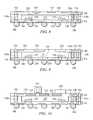
- FIG. 1illustrates electronic device 50 having a chip carrier substrate or PCB 52 with a plurality of semiconductor packages mounted on its surface.
- Electronic device 50may have one type of semiconductor package, or multiple types of semiconductor packages, depending on the application. The different types of semiconductor packages are shown in FIG. 1 for purposes of illustration.
- Electronic device 50may be a stand-alone system that uses the semiconductor packages to perform one or more electrical functions. Alternatively, electronic device 50 may be a subcomponent of a larger system. For example, electronic device 50 may be a graphics card, network interface card, or other signal processing card that can be inserted into a computer.
- the semiconductor packagecan include microprocessors, memories, application specific integrated circuits (ASICs), logic circuits, analog circuits, RF circuits, discrete devices, or other semiconductor die or electrical components.
- PCB 52provides a general substrate for structural support and electrical interconnect of the semiconductor packages mounted on the PCB.
- Conductive signal traces 54are formed over a surface or within layers of PCB 52 using evaporation, electrolytic plating, electroless plating, screen printing, or other suitable metal deposition process. Signal traces 54 provide for electrical communication between each of the semiconductor packages, mounted components, and other external system components. Traces 54 also provide power and ground connections to each of the semiconductor packages.
- a semiconductor devicehas two packaging levels.
- First level packagingis a technique for mechanically and electrically attaching the semiconductor die to an intermediate carrier.
- Second level packaginginvolves mechanically and electrically attaching the intermediate carrier to the PCB.
- a semiconductor devicemay only have the first level packaging where the die is mechanically and electrically mounted directly to the PCB.
- first level packagingincluding wire bond package 56 and flip chip 58
- second level packagingincluding ball grid array (BGA) 60 , bump chip carrier (BCC) 62 , dual in-line package (DIP) 64 , land grid array (LGA) 66 , multi-chip module (MCM) 68 , quad flat non-leaded package (QFN) 70 , and quad flat package 72 .
- BGAball grid array
- BCCbump chip carrier
- DIPdual in-line package
- LGAland grid array
- MCMmulti-chip module
- QFNquad flat non-leaded package
- quad flat package 72quad flat package
- electronic device 50includes a single attached semiconductor package, while other embodiments call for multiple interconnected packages.
- manufacturerscan incorporate pre-made components into electronic devices and systems. Because the semiconductor packages include sophisticated functionality, electronic devices can be manufactured using cheaper components and a streamlined manufacturing process. The resulting devices are less likely to fail and less expensive to manufacture resulting in a lower cost for consumers.
- FIGS. 2 a - 2 cshow exemplary semiconductor packages.
- FIG. 2 aillustrates further detail of DIP 64 mounted on PCB 52 .
- Semiconductor die 74includes an active region containing analog or digital circuits implemented as active devices, passive devices, conductive layers, and dielectric layers formed within the die and are electrically interconnected according to the electrical design of the die.
- the circuitmay include one or more transistors, diodes, inductors, capacitors, resistors, and other circuit elements formed within the active region of semiconductor die 74 .
- Contact pads 76are one or more layers of conductive material, such as aluminum (Al), copper (Cu), tin (Sn), nickel (Ni), gold (Au), or silver (Ag), and are electrically connected to the circuit elements formed within semiconductor die 74 .
- semiconductor die 74is mounted to an intermediate carrier 78 using a gold-silicon eutectic layer or adhesive material such as thermal epoxy.
- the package bodyincludes an insulative packaging material such as polymer or ceramic.
- Conductor leads 80 and wire bonds 82provide electrical interconnect between semiconductor die 74 and PCB 52 .
- Encapsulant 84is deposited over the package for environmental protection by preventing moisture and particles from entering the package and contaminating die 74 or wire bonds 82 .
- FIG. 2 billustrates further detail of BCC 62 mounted on PCB 52 .
- Semiconductor die 88is mounted over carrier 90 using an underfill or epoxy-resin adhesive material 92 .
- Wire bonds 94provide first level packing interconnect between contact pads 96 and 98 .
- Molding compound or encapsulant 100is deposited over semiconductor die 88 and wire bonds 94 to provide physical support and electrical isolation for the device.
- Contact pads 102are formed over a surface of PCB 52 using a suitable metal deposition such electrolytic plating or electroless plating to prevent oxidation.
- Contact pads 102are electrically connected to one or more conductive signal traces 54 in PCB 52 .
- Bumps 104are formed between contact pads 98 of BCC 62 and contact pads 102 of PCB 52 .
- semiconductor die 58is mounted face down to intermediate carrier 106 with a flip chip style first level packaging.
- Active region 108 of semiconductor die 58contains analog or digital circuits implemented as active devices, passive devices, conductive layers, and dielectric layers formed according to the electrical design of the die.
- the circuitmay include one or more transistors, diodes, inductors, capacitors, resistors, and other circuit elements within active region 108 .
- Semiconductor die 58is electrically and mechanically connected to carrier 106 through bumps 110 .
- BGA 60is electrically and mechanically connected to PCB 52 with a BGA style second level packaging using bumps 112 .
- Semiconductor die 58is electrically connected to conductive signal traces 54 in PCB 52 through bumps 110 , signal lines 114 , and bumps 112 .
- a molding compound or encapsulant 116is deposited over semiconductor die 58 and carrier 106 to provide physical support and electrical isolation for the device.
- the flip chip semiconductor deviceprovides a short electrical conduction path from the active devices on semiconductor die 58 to conduction tracks on PCB 52 in order to reduce signal propagation distance, lower capacitance, and improve overall circuit performance.
- the semiconductor die 58can be mechanically and electrically connected directly to PCB 52 using flip chip style first level packaging without intermediate carrier 106 .
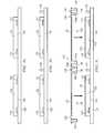
- FIGS. 3 a - 3 killustrate a process of forming a semiconductor device having 3D inductors made with a prefabricated pillar frame placed over semiconductor die and inductor core.
- a sacrificial or temporary reusable substrate or carrier 120contains base material such as silicon, polymer, polymer composite, metal, ceramic, glass, glass epoxy, beryllium oxide, tape, or other suitable low-cost, rigid material for structural support.
- Semiconductor die or components 122are mounted to carrier 120 with contact pads 124 oriented downward over the carrier.
- Semiconductor die 122each include an active region 126 containing analog or digital circuits implemented as active devices, passive devices, conductive layers, and dielectric layers formed within the die and electrically interconnected according to the electrical design and function of the die.
- the circuitmay include one or more transistors, diodes, and other circuit elements formed within active surface 126 to implement baseband analog circuits or digital circuits, such as digital signal processor (DSP), ASIC, memory, or other signal processing circuit.
- DSPdigital signal processor
- Semiconductor die 122may also contain IPD, such as inductors, capacitors, and resistors, for RF signal processing.
- IPDsuch as inductors, capacitors, and resistors, for RF signal processing.
- Semiconductor die 122can be a flipchip type device or wire bond type device. In another embodiment, a discrete component can be mounted over carrier 120 .
- a preformed inductor core 128is mounted over carrier 120 between semiconductor die 122 .
- the inductor core 128is typically surface mounted at designated locations on carrier 120 .
- inductor core 128can be deposited by PVD, CVD, or other suitable deposition process.
- the inductor core 128can be suitable either crystalline or non-crystalline ferromagnetic material or ferromagnetic composite material.
- inductor core 128can include alloys such as FeOFe2O3, NiOFe2O3, CuOFe2O3, or MgOFe2O3.
- a prefabricated pillar frame 130is mounted over semiconductor die 122 and inductor core 128 , as shown in FIGS. 3 c - 3 d.
- prefabricated pillar frame 130is made with Cu using leadframe technology.
- Pillar frame 130includes a flat plate 132 with a plurality of bodies 134 a - 134 f integrated with plate 132 and separated by cavities 136 .
- Bodies 134 a - 134 fare sufficiently thick to extend down to carrier 120 when pillar frame 130 is mounted over semiconductor die 122 .
- An optional adhesive or thermal interface material 138provides a secure physical contact between plate 132 and a back surface of semiconductor die 122 .
- a plurality of openings 140is formed through plate 132 into cavities 136 .
- the prefabricated pillar frame 130is simple to manufacture and cost effective in comparison to the plated TMV pillars discussed in the background.
- FIG. 3 dshows pillar frame 130 mounted over semiconductor die 122 .
- Bodies 134 a and 134 dare vertical (z-direction) interconnect pillars.
- the inductor core 128is disposed in cavity 136 between bodies 134 b - 134 c and between bodies 134 e - 134 f.
- Bodies 134 b, 134 c, 134 e, and 134 fare inductor pillars around inductor core 128 .
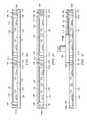
- FIG. 3 eshows an encapsulant or molding compound 146 deposited over semiconductor die 122 and prefabricated pillar frame 130 using a paste printing, compressive molding, transfer molding, liquid encapsulant molding, vacuum lamination, or other suitable applicator.
- the encapsulation processdisperses encapsulant 146 through openings 140 into cavities 136 below pillar frame 130 .
- Encapsulant 146can be polymer composite material, such as epoxy resin with filler, epoxy acrylate with filler, or polymer with proper filler.
- Encapsulant 146is non-conductive and environmentally protects the semiconductor device from external elements and contaminants.
- Encapsulant 146encloses semiconductor die 122 , inductor core 128 , and bodies 134 a - 34 f.
- grinder 148removes a portion of pillar frame 130 , including plate 132 and adhesive layer 138 , to planarize the surface and expose encapsulant 146 in cavities 136 .
- the remaining portion of pillar frame 130 between semiconductor die 122becomes conductive pillars or posts 134 a and 134 d for vertical z-direction interconnection, and inductor pillars 134 b, 134 c, 134 e, and 134 f for RF signal processing.
- the grindingcan be done after removing the sacrificial substrate or temporary carrier 120 .
- FIG. 3 gshows a top view of interconnect pillars 134 a around semiconductor die 122 and inductor pillars 134 b - 134 c around inductor core 128 , all enclosed in encapsulant 146 .
- a build-up interconnect structure 149is formed over the back surface of semiconductor die 122 , encapsulant 146 , interconnect pillars 134 a and 134 d, and inductor pillars 134 b - 134 c and 134 e - 134 f.
- the build-up interconnect structure 149includes at least one insulating or passivation layer.
- passivation layer 150is formed with PVD, CVD, printing, sintering, or thermal oxidation.
- the passivation layer 150can be dielectric polymer insulation materials, such as low temperature cured photosensitive resist.
- passivation layer 150can be one or more layers of silicon dioxide (SiO2), silicon nitride (Si3N4), silicon oxynitride (SiON), tantalum pentoxide (Ta2O5), aluminum oxide (Al2O3), or other material having similar insulating and structural properties.
- a portion of passivation layer 150is removed by an etching process to expose interconnect pillars 134 a and 134 d, and inductor pillars 134 b - 134 c and 134 e - 134 f.
- the build-up interconnect structure 149further includes at least one electrically conductive layer 152 formed over or between passivation layers, for example, over passivation layer 150 .
- Conductive layer 152can be one or more layers of Al, Cu, Sn, Ni, Au, Ag, or other suitable electrically conductive material.
- Conductive layer 152is electrically connected to interconnect pillars 134 a and 134 d to provide vertical, z-direction interconnect.
- Conductive layer 152is also electrically connected between rows of inductor pillars 134 b - 134 c and 134 e - 134 f, as shown in FIG. 3 j , to provide an integrated 3D inductor coiled around inductor core 128 .
- carrier 120is removed by chemical etching, mechanical peel-off, CMP, mechanical grinding, thermal bake, laser scanning, or wet stripping.
- a build-up interconnect structure 153is formed over the front surface of semiconductor die 122 , encapsulant 146 , interconnect pillars 134 a and 134 d, and inductor pillars 134 b - 134 c and 134 e - 134 f.
- the build-up interconnect structure 153includes at least one insulating or passivation layer 154 formed with PVD, CVD, printing, sintering, or thermal oxidation.
- the passivation layer 154can be dielectric polymer insulation materials, such as low temperature cured photosensitive resist.
- passivation layer 154can be one or more layers of SiO2, Si3N4, SiON, Ta2O5, Al2O3, or other material having similar insulating and structural properties. A portion of passivation layer 154 is removed by an etching process to expose interconnect pillars 134 a and 134 d, and inductor pillars 134 b - 134 c and 134 e - 134 f.
- the build-up interconnect structure 153further includes at least one electrically conductive layer 156 formed over or between passivation layers, for example over passivation layer 154 , interconnect pillars 134 a and 134 d, and inductor pillars 134 b - 134 c and 134 e - 134 f using patterning with PVD, CVD, sputtering, electrolytic plating, electroless plating process, or other suitable metal deposition process.
- Conductive layer 156can be one or more layers of Al, Cu, Sn, Ni, Au, Ag, or other suitable electrically conductive material.
- Conductive layer 156is electrically connected to interconnect pillars 134 a and 134 d to provide vertical, z-direction interconnect.
- Conductive layer 156is also electrically connected between rows of inductor pillars 134 b - 134 c and 134 e - 134 f, as shown in FIG. 3 j , to provide an integrated 3D inductor coiled around inductor core 128 .
- Conductive layer 156is electrically connected to contact pads 124 .
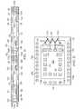
- semiconductor die or components 158are mounted over build-up interconnect structure 149 .
- Solder bumps 160are electrically connected to conductive layer 152 .
- An optional underfill material 162is deposited between semiconductor die 158 and conductive layer 152 .
- Semiconductor die 158each include a substrate and active region containing analog or digital circuits implemented as active devices, passive devices, conductive layers, and dielectric layers formed within the die and electrically interconnected according to the electrical design and function of the die.
- the circuitmay include one or more transistors, diodes, and other circuit elements formed within its active surface to implement baseband analog circuits or digital circuits, such as DSP, ASIC, memory, or other signal processing circuit.
- Semiconductor die 158may also contain IPD, such as inductors, capacitors, and resistors, for RF signal processing.
- IPDinductors, capacitors, and resistors
- Semiconductor die 158can be a flipchip type device or wire bond type device.
- a discrete semiconductor componentcan be mounted over semiconductor die 122 .
- the discrete semiconductor componentcan be a resistor, capacitor, inductor, or active semiconductor device.
- An electrically conductive materialis deposited over conductive layer 156 using an evaporation, electrolytic plating, electroless plating, ball drop, or screen printing process.
- the conductive materialcan be Al, Sn, Ni, Au, Ag, Pb, Bi, Cu, solder, and combinations thereof, with an optional flux material.
- the conductive materialcan be eutectic Sn/Pb, high-lead solder, or lead-free solder.
- the conductive materialis bonded to conductive layer 156 using a suitable attachment or bonding process. In one embodiment, the conductive material is reflowed by heating the material above its melting point to form spherical balls or bumps 166 .
- bumps 166are reflowed a second time to improve electrical contact to conductive layer 156 .
- the bumpscan also be compression bonded to conductive layer 156 .
- Bumps 166represent one type of interconnect structure that can be formed over conductive layer 156 .
- the interconnect structurecan also use bond wires, conductive paste, stud bump, micro bump, or other electrical interconnect.
- the structureis singulated with saw blade or laser cutting tool 164 into individual semiconductor devices 168 .
- the IPDs in semiconductor device 168including the 3D inductor, provide the electrical characteristics needed for high frequency applications, such as resonators, high-pass filters, low-pass filters, band-pass filters, symmetric Hi-Q resonant transformers, matching networks, and tuning capacitors.
- the IPDscan be used as front-end wireless RF components, which can be positioned between the antenna and transceiver.
- the inductorcan be a hi-Q balun, transformer, or coil, operating up to 100 Gigahertz. In some applications, multiple baluns are formed on a same substrate, allowing multi-band operation.
- balunsare used in a quad-band for mobile phones or other global system for mobile (GSM) communications, each balun dedicated for a frequency band of operation of the quad-band device.
- GSMglobal system for mobile
- a typical RF systemrequires multiple IPDs and other high frequency circuits in one or more semiconductor packages to perform the necessary electrical functions.
- FIG. 4shows an embodiment of the semiconductor device having the 3D inductor made with the prefabricated pillar frame, without the interconnect pillars.
- the inductor pillars 170 a and 170 bare formed around inductor core 172 , using a process similar to FIGS. 3 a - 3 k.
- the build-up interconnect layer 149can be optional if passivation layer 150 is part of the encapsulation and conductive layer 152 is fabricated in lead frame technology by half etching other portions of the frame.
- FIG. 5shows an embodiment of the semiconductor device with multiple 3D inductors made with the prefabricated pillar frame.
- the inductor pillars 180 a and 180 bare formed around inductor core 182
- inductor pillars 180 c and 180 dare formed around inductor core 184 , using a process similar to FIGS. 3 a - 3 k .
- the build-up interconnect layer 149can be optional if passivation 150 is part of the encapsulation and conductive layer 152 is fabricated in lead frame technology by half etching other portions of the frame.
- FIG. 6shows an embodiment of the semiconductor device having stacked semiconductor die and multiple 3D inductors made with the prefabricated pillar frame.
- a back surface of semiconductor die 190is mounted to a back surface of semiconductor die 192 with an adhesive 193 .
- Contact pads 194 of semiconductor die 190are oriented upward and electrically connect to conductive layer 152 of build-up interconnect structure 149 .
- Contact pads 196 of semiconductor die 192are oriented downward and electrically connect to conductive layer 156 of build-up interconnect structure 153 .
- the inductor pillars 198 a and 198 bare formed around inductor core 200
- inductor pillars 198 c and 198 dare formed around inductor core 202 , using a process similar to FIGS. 3 a - 3 k.
- FIG. 7shows an embodiment of the semiconductor device having side-by-side semiconductor die 206 and multiple 3D inductors made with the prefabricated pillar frame.
- Contact pads 208 of semiconductor die 206are oriented downward and electrically connect to conductive layer 156 of build-up interconnect structure 153 .
- the inductor pillars 210 a and 210 bare formed around inductor core 212
- inductor pillars 210 c and 210 dare formed around inductor core 214 , using a process similar to FIGS. 3 a - 3 k.
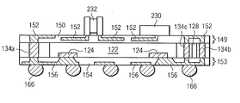
- FIG. 8shows an embodiment of the semiconductor device with the 3D inductor made with the prefabricated pillar frame and a shielding layer 220 formed over semiconductor die 122 to reduce inter-device interference of the IPD.
- Shielding layer 220can be Cu, Al, ferrite or carbonyl iron, stainless steel, nickel silver, low-carbon steel, silicon-iron steel, foil, epoxy, conductive resin, and other metals and composites capable of blocking or absorbing EMI, RFI, and other inter-device interference.
- Shielding layer 220can also be a non-metal material such as carbon-black or aluminum flake to reduce the effects of EMI and RFI. Shielding layer 220 thermally contacts the backside of semiconductor die 122 .
- Shielding layer 220is electrically connected to a low-impedance ground point through conductive layer 152 , interconnect pillars 134 a, and solder bump 166 . Shielding layer 220 also dissipates heat generated by semiconductor die 122 .
- the semiconductor device with the 3D inductor made with the prefabricated pillar framefurther includes a thin film capacitor 222 is formed in build-up interconnect layer 149 , and thin film capacitor 224 is formed in build-up interconnect layer 153 .
- a thin film resistor 226is formed in build-up interconnect layer 149
- thin film resistor 228is formed in build-up interconnect layer 153 .
- the thin film capacitors 222 - 224 and thin film resistor 226 - 228constitute additional IPDs that can be formed in build-up interconnect structures 149 and 153 .
- the semiconductor device with 3D inductor made with the prefabricated pillar framefurther includes discrete semiconductor components 230 and 232 are formed over build-up interconnect layer 149 and electrically connected to conductive layer 152 .
Landscapes
- Engineering & Computer Science (AREA)
- Power Engineering (AREA)
- Computer Hardware Design (AREA)
- Microelectronics & Electronic Packaging (AREA)
- Physics & Mathematics (AREA)
- General Physics & Mathematics (AREA)
- Condensed Matter Physics & Semiconductors (AREA)
- Health & Medical Sciences (AREA)
- Electromagnetism (AREA)
- Toxicology (AREA)
- Manufacturing & Machinery (AREA)
- Semiconductor Integrated Circuits (AREA)
- Structures Or Materials For Encapsulating Or Coating Semiconductor Devices Or Solid State Devices (AREA)
- Production Of Multi-Layered Print Wiring Board (AREA)
Abstract
Description
- The present application is a continuation of U.S. patent application Ser. No. 12/467,908, filed May 18, 2009, and claims priority to the foregoing parent application pursuant to 35 U.S.C. §120.
- The present invention relates in general to semiconductor devices and, more particularly, to a semiconductor device and method of forming a 3D inductor from a prefabricated pillar frame.
- Semiconductor devices are commonly found in modern electronic products. Semiconductor devices vary in the number and density of electrical components. Discrete semiconductor devices generally contain one type of electrical component, e.g., light emitting diode (LED), small signal transistor, resistor, capacitor, inductor, and power metal oxide semiconductor field effect transistor (MOSFET). Integrated semiconductor devices typically contain hundreds to millions of electrical components. Examples of integrated semiconductor devices include microcontrollers, microprocessors, charged-coupled devices (CCDs), solar cells, and digital micro-mirror devices (DMDs).
- Semiconductor devices perform a wide range of functions such as high-speed calculations, transmitting and receiving electromagnetic signals, controlling electronic devices, transforming sunlight to electricity, and creating visual projections for television displays. Semiconductor devices are found in the fields of entertainment, communications, power conversion, networks, computers, and consumer products. Semiconductor devices are also found in military applications, aviation, automotive, industrial controllers, and office equipment.
- Semiconductor devices exploit the electrical properties of semiconductor materials. The atomic structure of semiconductor material allows its electrical conductivity to be manipulated by the application of an electric field or through the process of doping. Doping introduces impurities into the semiconductor material to manipulate and control the conductivity of the semiconductor device.
- A semiconductor device contains active and passive electrical structures. Active structures, including bipolar and field effect transistors, control the flow of electrical current. By varying levels of doping and application of an electric field or base current, the transistor either promotes or restricts the flow of electrical current. Passive structures, including resistors, capacitors, and inductors, create a relationship between voltage and current necessary to perform a variety of electrical functions. The passive and active structures are electrically connected to form circuits, which enable the semiconductor device to perform high-speed calculations and other useful functions.
- Semiconductor devices are generally manufactured using two complex manufacturing processes, i.e., front-end manufacturing, and back-end manufacturing, each involving potentially hundreds of steps. Front-end manufacturing involves the formation of a plurality of die on the surface of a semiconductor wafer. Each die is typically identical and contains circuits formed by electrically connecting active and passive components. Back-end manufacturing involves singulating individual die from the finished wafer and packaging the die to provide structural support and environmental isolation.
- One goal of semiconductor manufacturing is to produce smaller semiconductor devices. Smaller devices typically consume less power, have higher performance, and can be produced more efficiently. In addition, smaller semiconductor devices have a smaller footprint, which is desirable for smaller end products. A smaller die size may be achieved by improvements in the front-end process resulting in die with smaller, higher density active and passive components. Back-end processes may result in semiconductor device packages with a smaller footprint by improvements in electrical interconnection and packaging materials.
- Another goal of semiconductor manufacturing is to produce higher performance semiconductor devices. Increases in device performance can be accomplished by forming active components that are capable of operating at higher speeds. In high frequency applications, such as radio frequency (RF) wireless communications, integrated passive devices (IPDs) are often contained within the semiconductor device. Examples of IPDs include resistors, capacitors, and inductors. A typical RF system requires multiple IPDs in one or more semiconductor packages to perform the necessary electrical functions.
- An integrated three dimensional (3D) inductor can be made by forming through mold via (TMV) in the encapsulant around a ferromagnetic core material, as described in US Publication 20080135977. The TMVs are plated to form metal inductor pillars which are electrically connected in a coiled arrangement around the ferromagnetic core. The lithography and plating processes needed to form the inductor pillars are time consuming and costly.
- A need exists for 3D inductors without using costly lithography and plating processes to form the inductor pillars. Accordingly, in one embodiment, the present invention is a method of making a semiconductor device comprising the steps of providing a carrier, mounting a semiconductor component over the carrier, forming an inductor core over the carrier, and mounting a pillar frame over the carrier and semiconductor component. The pillar frame includes a plurality of bodies with a first portion of the bodies being disposed around the inductor core. The method further includes the steps of depositing an encapsulant around the semiconductor component, plurality of bodies, and inductor core, removing a portion of the pillar frame while leaving the first portion of the bodies to form inductor pillars, forming a first interconnect structure over a first surface of the encapsulant, removing the carrier, and forming a second interconnect structure over a second surface of the encapsulant opposite the first interconnect structure. The first and second interconnect structures are electrically connected to the inductor pillars to form a 3D inductor.
- In another embodiment, the present invention is a method of making a semiconductor device comprising the steps of providing a carrier, mounting a semiconductor component over the carrier, mounting a pillar frame over the carrier and semiconductor component, depositing an encapsulant over the semiconductor component and pillar frame, and removing a portion of the pillar frame. A first remaining portion of the pillar frame provides inductor pillars. The method further includes the steps of forming a first interconnect structure over a first surface of the encapsulant, removing the carrier, and forming a second interconnect structure over a second surface of the encapsulant opposite the first interconnect structure. The first and second interconnect structures are electrically connected to the inductor pillars to form a 3D inductor.
- In another embodiment, the present invention is a method of making a semiconductor device comprising the steps of providing a carrier, mounting a semiconductor component over the carrier, mounting a pillar frame over the carrier and semiconductor component, depositing an encapsulant over the semiconductor component and pillar frame, removing a portion of the pillar frame, and forming a first interconnect structure over a first surface of the encapsulant. A first remaining portion of the pillar frame provides inductor pillars. The first interconnect structure is electrically connected to the inductor pillars to form a 3D inductor.
- In another embodiment, the present invention is a semiconductor device comprising a semiconductor component and inductor core disposed in proximity to the semiconductor component. A pillar frame is mounted over the semiconductor component and inductor core. An encapsulant is deposited over the semiconductor component, pillar frame, and inductor core. A portion of the pillar frame is removed to form inductor pillars around the inductor core. A first interconnect structure is formed over a first surface of the encapsulant. A second interconnect structure is formed over a second surface of the encapsulant opposite the first interconnect structure. The first and second interconnect structures are electrically connected to the inductor pillars to form one or more 3D inductors.
FIG. 1 illustrates a PCB with different types of packages mounted to its surface;FIGS. 2 a-2cillustrate further detail of the representative semiconductor packages mounted to the PCB;FIGS. 3 a-3killustrate a process of using a prefabricated pillar frame to form interconnect pillars and inductor pillars around an inductor core;FIG. 4 illustrates the semiconductor device with 3D inductors and without interconnect pillars;FIG. 5 illustrates the semiconductor device having multiple 3D inductors;FIG. 6 illustrates stacked semiconductor die with 3D inductors and interconnect pillars;FIG. 7 illustrates side-by-side semiconductor die with 3D inductors and interconnect pillars;FIG. 8 illustrates the semiconductor device with 3D inductors and a shielding layer formed over the semiconductor die;FIG. 9 illustrates the semiconductor device with 3D inductors and capacitor and resistor formed in build-up interconnect structure; andFIG. 10 illustrates the semiconductor device with 3D inductors and discrete semiconductor components formed over the build-up interconnect layer.- The present invention is described in one or more embodiments in the following description with reference to the figures, in which like numerals represent the same or similar elements. While the invention is described in terms of the best mode for achieving the invention's objectives, it will be appreciated by those skilled in the art that it is intended to cover alternatives, modifications, and equivalents as may be included within the spirit and scope of the invention as defined by the appended claims and their equivalents as supported by the following disclosure and drawings.
- Semiconductor devices are generally manufactured using two complex manufacturing processes: front-end manufacturing and back-end manufacturing. Front-end manufacturing involves the formation of a plurality of die on the surface of a semiconductor wafer. Each die on the wafer contains active and passive electrical components, which are electrically connected to form functional electrical circuits. Active electrical components, such as transistors and diodes, have the ability to control the flow of electrical current. Passive electrical components, such as capacitors, inductors, resistors, and transformers, create a relationship between voltage and current necessary to perform electrical circuit functions.
- Passive and active components are formed over the surface of the semiconductor wafer by a series of process steps including doping, deposition, photolithography, etching, and planarization. Doping introduces impurities into the semiconductor material by techniques such as ion implantation or thermal diffusion. The doping process modifies the electrical conductivity of semiconductor material in active devices, transforming the semiconductor material into an insulator, conductor, or dynamically changing the semiconductor material conductivity in response to an electric field or base current. Transistors contain regions of varying types and degrees of doping arranged as necessary to enable the transistor to promote or restrict the flow of electrical current upon the application of the electric field or base current.
- Active and passive components are formed by layers of materials with different electrical properties. The layers can be formed by a variety of deposition techniques determined in part by the type of material being deposited. For example, thin film deposition may involve chemical vapor deposition (CVD), physical vapor deposition (PVD), electrolytic plating, and electroless plating processes. Each layer is generally patterned to form portions of active components, passive components, or electrical connections between components.
- The layers can be patterned using photolithography, which involves the deposition of light sensitive material, e.g., photoresist, over the layer to be patterned. A pattern is transferred from a photomask to the photoresist using light. The portion of the photoresist pattern subjected to light is removed using a solvent, exposing portions of the underlying layer to be patterned. The remainder of the photoresist is removed, leaving behind a patterned layer. Alternatively, some types of materials are patterned by directly depositing the material into the areas or voids formed by a previous deposition/etch process using techniques such as electroless and electrolytic plating.
- Depositing a thin film of material over an existing pattern can exaggerate the underlying pattern and create a non-uniformly flat surface. A uniformly flat surface is required to produce smaller and more densely packed active and passive components. Planarization can be used to remove material from the surface of the wafer and produce a uniformly flat surface. Planarization involves polishing the surface of the wafer with a polishing pad. An abrasive material and corrosive chemical are added to the surface of the wafer during polishing. The combined mechanical action of the abrasive and corrosive action of the chemical removes any irregular topography, resulting in a uniformly flat surface.
- Back-end manufacturing refers to cutting or singulating the finished wafer into the individual die and then packaging the die for structural support and environmental isolation. To singulate the die, the wafer is scored and broken along non-functional regions of the wafer called saw streets or scribes. The wafer is singulated using a laser cutting tool or saw blade. After singulation, the individual die are mounted to a package substrate that includes pins or contact pads for interconnection with other system components. Contact pads formed over the semiconductor die are then connected to contact pads within the package. The electrical connections can be made with solder bumps, stud bumps, conductive paste, or wirebonds. An encapsulant or other molding material is deposited over the package to provide physical support and electrical isolation. The finished package is then inserted into an electrical system and the functionality of the semiconductor device is made available to the other system components.
FIG. 1 illustrateselectronic device 50 having a chip carrier substrate orPCB 52 with a plurality of semiconductor packages mounted on its surface.Electronic device 50 may have one type of semiconductor package, or multiple types of semiconductor packages, depending on the application. The different types of semiconductor packages are shown inFIG. 1 for purposes of illustration.Electronic device 50 may be a stand-alone system that uses the semiconductor packages to perform one or more electrical functions. Alternatively,electronic device 50 may be a subcomponent of a larger system. For example,electronic device 50 may be a graphics card, network interface card, or other signal processing card that can be inserted into a computer. The semiconductor package can include microprocessors, memories, application specific integrated circuits (ASICs), logic circuits, analog circuits, RF circuits, discrete devices, or other semiconductor die or electrical components.- In
FIG. 1 ,PCB 52 provides a general substrate for structural support and electrical interconnect of the semiconductor packages mounted on the PCB. Conductive signal traces54 are formed over a surface or within layers ofPCB 52 using evaporation, electrolytic plating, electroless plating, screen printing, or other suitable metal deposition process. Signal traces54 provide for electrical communication between each of the semiconductor packages, mounted components, and other external system components.Traces 54 also provide power and ground connections to each of the semiconductor packages. - In some embodiments, a semiconductor device has two packaging levels. First level packaging is a technique for mechanically and electrically attaching the semiconductor die to an intermediate carrier. Second level packaging involves mechanically and electrically attaching the intermediate carrier to the PCB. In other embodiments, a semiconductor device may only have the first level packaging where the die is mechanically and electrically mounted directly to the PCB.
- For the purpose of illustration, several types of first level packaging, including
wire bond package 56 andflip chip 58, are shown onPCB 52. Additionally, several types of second level packaging, including ball grid array (BGA)60, bump chip carrier (BCC)62, dual in-line package (DIP)64, land grid array (LGA)66, multi-chip module (MCM)68, quad flat non-leaded package (QFN)70, and quadflat package 72, are shown mounted onPCB 52. Depending upon the system requirements, any combination of semiconductor packages, configured with any combination of first and second level packaging styles, as well as other electronic components, can be connected toPCB 52. In some embodiments,electronic device 50 includes a single attached semiconductor package, while other embodiments call for multiple interconnected packages. By combining one or more semiconductor packages over a single substrate, manufacturers can incorporate pre-made components into electronic devices and systems. Because the semiconductor packages include sophisticated functionality, electronic devices can be manufactured using cheaper components and a streamlined manufacturing process. The resulting devices are less likely to fail and less expensive to manufacture resulting in a lower cost for consumers. FIGS. 2 a-2cshow exemplary semiconductor packages.FIG. 2 aillustrates further detail ofDIP 64 mounted onPCB 52. Semiconductor die74 includes an active region containing analog or digital circuits implemented as active devices, passive devices, conductive layers, and dielectric layers formed within the die and are electrically interconnected according to the electrical design of the die. For example, the circuit may include one or more transistors, diodes, inductors, capacitors, resistors, and other circuit elements formed within the active region of semiconductor die74. Contactpads 76 are one or more layers of conductive material, such as aluminum (Al), copper (Cu), tin (Sn), nickel (Ni), gold (Au), or silver (Ag), and are electrically connected to the circuit elements formed within semiconductor die74. During assembly ofDIP 64, semiconductor die74 is mounted to anintermediate carrier 78 using a gold-silicon eutectic layer or adhesive material such as thermal epoxy. The package body includes an insulative packaging material such as polymer or ceramic. Conductor leads80 andwire bonds 82 provide electrical interconnect between semiconductor die74 andPCB 52.Encapsulant 84 is deposited over the package for environmental protection by preventing moisture and particles from entering the package and contaminating die74 or wire bonds82.FIG. 2 billustrates further detail ofBCC 62 mounted onPCB 52. Semiconductor die88 is mounted overcarrier 90 using an underfill or epoxy-resin adhesive material 92.Wire bonds 94 provide first level packing interconnect betweencontact pads encapsulant 100 is deposited over semiconductor die88 andwire bonds 94 to provide physical support and electrical isolation for the device. Contactpads 102 are formed over a surface ofPCB 52 using a suitable metal deposition such electrolytic plating or electroless plating to prevent oxidation. Contactpads 102 are electrically connected to one or more conductive signal traces54 inPCB 52.Bumps 104 are formed betweencontact pads 98 ofBCC 62 andcontact pads 102 ofPCB 52.- In
FIG. 2 c, semiconductor die58 is mounted face down tointermediate carrier 106 with a flip chip style first level packaging.Active region 108 of semiconductor die58 contains analog or digital circuits implemented as active devices, passive devices, conductive layers, and dielectric layers formed according to the electrical design of the die. For example, the circuit may include one or more transistors, diodes, inductors, capacitors, resistors, and other circuit elements withinactive region 108. Semiconductor die58 is electrically and mechanically connected tocarrier 106 throughbumps 110. BGA 60 is electrically and mechanically connected toPCB 52 with a BGA style second levelpackaging using bumps 112. Semiconductor die58 is electrically connected to conductive signal traces54 inPCB 52 throughbumps 110,signal lines 114, and bumps112. A molding compound orencapsulant 116 is deposited over semiconductor die58 andcarrier 106 to provide physical support and electrical isolation for the device. The flip chip semiconductor device provides a short electrical conduction path from the active devices on semiconductor die58 to conduction tracks onPCB 52 in order to reduce signal propagation distance, lower capacitance, and improve overall circuit performance. In another embodiment, the semiconductor die58 can be mechanically and electrically connected directly toPCB 52 using flip chip style first level packaging withoutintermediate carrier 106.FIGS. 3 a-3killustrate a process of forming a semiconductor device having 3D inductors made with a prefabricated pillar frame placed over semiconductor die and inductor core. InFIG. 3 a, a sacrificial or temporary reusable substrate orcarrier 120 contains base material such as silicon, polymer, polymer composite, metal, ceramic, glass, glass epoxy, beryllium oxide, tape, or other suitable low-cost, rigid material for structural support.- Semiconductor die or
components 122 are mounted tocarrier 120 withcontact pads 124 oriented downward over the carrier. Semiconductor die122 each include anactive region 126 containing analog or digital circuits implemented as active devices, passive devices, conductive layers, and dielectric layers formed within the die and electrically interconnected according to the electrical design and function of the die. For example, the circuit may include one or more transistors, diodes, and other circuit elements formed withinactive surface 126 to implement baseband analog circuits or digital circuits, such as digital signal processor (DSP), ASIC, memory, or other signal processing circuit. Semiconductor die122 may also contain IPD, such as inductors, capacitors, and resistors, for RF signal processing. Semiconductor die122 can be a flipchip type device or wire bond type device. In another embodiment, a discrete component can be mounted overcarrier 120. - A preformed
inductor core 128 is mounted overcarrier 120 between semiconductor die122. Theinductor core 128 is typically surface mounted at designated locations oncarrier 120. Alternatively,inductor core 128 can be deposited by PVD, CVD, or other suitable deposition process. Theinductor core 128 can be suitable either crystalline or non-crystalline ferromagnetic material or ferromagnetic composite material. In other embodiment,inductor core 128 can include alloys such as FeOFe2O3, NiOFe2O3, CuOFe2O3, or MgOFe2O3. - A
prefabricated pillar frame 130 is mounted over semiconductor die122 andinductor core 128, as shown inFIGS. 3 c-3d.In one embodiment,prefabricated pillar frame 130 is made with Cu using leadframe technology.Pillar frame 130 includes aflat plate 132 with a plurality of bodies134a-134fintegrated withplate 132 and separated bycavities 136. Bodies134a-134fare sufficiently thick to extend down tocarrier 120 whenpillar frame 130 is mounted over semiconductor die122. An optional adhesive orthermal interface material 138 provides a secure physical contact betweenplate 132 and a back surface of semiconductor die122. A plurality ofopenings 140 is formed throughplate 132 intocavities 136. Theprefabricated pillar frame 130 is simple to manufacture and cost effective in comparison to the plated TMV pillars discussed in the background. FIG. 3 dshowspillar frame 130 mounted over semiconductor die122.Bodies inductor core 128 is disposed incavity 136 betweenbodies 134b-134cand between bodies134e-134f.Bodies inductor core 128.FIG. 3 eshows an encapsulant ormolding compound 146 deposited over semiconductor die122 andprefabricated pillar frame 130 using a paste printing, compressive molding, transfer molding, liquid encapsulant molding, vacuum lamination, or other suitable applicator. The encapsulation process disperses encapsulant146 throughopenings 140 intocavities 136 belowpillar frame 130.Encapsulant 146 can be polymer composite material, such as epoxy resin with filler, epoxy acrylate with filler, or polymer with proper filler.Encapsulant 146 is non-conductive and environmentally protects the semiconductor device from external elements and contaminants.Encapsulant 146 encloses semiconductor die122,inductor core 128, and bodies134a-34f.- In
FIG. 3 f,grinder 148 removes a portion ofpillar frame 130, includingplate 132 andadhesive layer 138, to planarize the surface and exposeencapsulant 146 incavities 136. The remaining portion ofpillar frame 130 between semiconductor die122 becomes conductive pillars orposts inductor pillars temporary carrier 120.FIG. 3 gshows a top view ofinterconnect pillars 134aaround semiconductor die122 andinductor pillars 134b-134caroundinductor core 128, all enclosed inencapsulant 146. - In
FIG. 3 h, a build-upinterconnect structure 149 is formed over the back surface of semiconductor die122,encapsulant 146,interconnect pillars inductor pillars 134b-134cand134e-134f.The build-upinterconnect structure 149 includes at least one insulating or passivation layer. For example,passivation layer 150 is formed with PVD, CVD, printing, sintering, or thermal oxidation. Thepassivation layer 150 can be dielectric polymer insulation materials, such as low temperature cured photosensitive resist. Alternatively,passivation layer 150 can be one or more layers of silicon dioxide (SiO2), silicon nitride (Si3N4), silicon oxynitride (SiON), tantalum pentoxide (Ta2O5), aluminum oxide (Al2O3), or other material having similar insulating and structural properties. A portion ofpassivation layer 150 is removed by an etching process to exposeinterconnect pillars inductor pillars 134b-134cand134e-134f. - The build-up
interconnect structure 149 further includes at least one electricallyconductive layer 152 formed over or between passivation layers, for example, overpassivation layer 150.Conductive interconnect pillars inductor pillars 134b-134cand134e-134fusing patterning with PVD, CVD, sputtering, electrolytic plating, electroless plating process, or other suitable metal deposition process.Conductive layer 152 can be one or more layers of Al, Cu, Sn, Ni, Au, Ag, or other suitable electrically conductive material.Conductive layer 152 is electrically connected to interconnectpillars Conductive layer 152 is also electrically connected between rows ofinductor pillars 134b-134cand134e-134f,as shown inFIG. 3 j, to provide an integrated 3D inductor coiled aroundinductor core 128. - In
FIG. 3 i,carrier 120 is removed by chemical etching, mechanical peel-off, CMP, mechanical grinding, thermal bake, laser scanning, or wet stripping. A build-upinterconnect structure 153 is formed over the front surface of semiconductor die122,encapsulant 146,interconnect pillars inductor pillars 134b-134cand134e-134f.The build-upinterconnect structure 153 includes at least one insulating orpassivation layer 154 formed with PVD, CVD, printing, sintering, or thermal oxidation. Thepassivation layer 154 can be dielectric polymer insulation materials, such as low temperature cured photosensitive resist. Alternatively,passivation layer 154 can be one or more layers of SiO2, Si3N4, SiON, Ta2O5, Al2O3, or other material having similar insulating and structural properties. A portion ofpassivation layer 154 is removed by an etching process to exposeinterconnect pillars inductor pillars 134b-134cand134e-134f. - The build-up
interconnect structure 153 further includes at least one electricallyconductive layer 156 formed over or between passivation layers, for example overpassivation layer 154,interconnect pillars inductor pillars 134b-134cand134e-134fusing patterning with PVD, CVD, sputtering, electrolytic plating, electroless plating process, or other suitable metal deposition process.Conductive layer 156 can be one or more layers of Al, Cu, Sn, Ni, Au, Ag, or other suitable electrically conductive material.Conductive layer 156 is electrically connected to interconnectpillars Conductive layer 156 is also electrically connected between rows ofinductor pillars 134b-134cand134e-134f,as shown inFIG. 3 j, to provide an integrated 3D inductor coiled aroundinductor core 128.Conductive layer 156 is electrically connected to contactpads 124. - In
FIG. 3 k, semiconductor die orcomponents 158 are mounted over build-upinterconnect structure 149. Solder bumps160 are electrically connected toconductive layer 152. Anoptional underfill material 162 is deposited between semiconductor die158 andconductive layer 152. Semiconductor die158 each include a substrate and active region containing analog or digital circuits implemented as active devices, passive devices, conductive layers, and dielectric layers formed within the die and electrically interconnected according to the electrical design and function of the die. For example, the circuit may include one or more transistors, diodes, and other circuit elements formed within its active surface to implement baseband analog circuits or digital circuits, such as DSP, ASIC, memory, or other signal processing circuit. Semiconductor die158 may also contain IPD, such as inductors, capacitors, and resistors, for RF signal processing. Semiconductor die158 can be a flipchip type device or wire bond type device. In another embodiment, a discrete semiconductor component can be mounted over semiconductor die122. The discrete semiconductor component can be a resistor, capacitor, inductor, or active semiconductor device. - An electrically conductive material is deposited over
conductive layer 156 using an evaporation, electrolytic plating, electroless plating, ball drop, or screen printing process. The conductive material can be Al, Sn, Ni, Au, Ag, Pb, Bi, Cu, solder, and combinations thereof, with an optional flux material. For example, the conductive material can be eutectic Sn/Pb, high-lead solder, or lead-free solder. The conductive material is bonded toconductive layer 156 using a suitable attachment or bonding process. In one embodiment, the conductive material is reflowed by heating the material above its melting point to form spherical balls or bumps166. In some applications, bumps166 are reflowed a second time to improve electrical contact toconductive layer 156. The bumps can also be compression bonded toconductive layer 156.Bumps 166 represent one type of interconnect structure that can be formed overconductive layer 156. The interconnect structure can also use bond wires, conductive paste, stud bump, micro bump, or other electrical interconnect. - The structure is singulated with saw blade or
laser cutting tool 164 intoindividual semiconductor devices 168. The IPDs insemiconductor device 168, including the 3D inductor, provide the electrical characteristics needed for high frequency applications, such as resonators, high-pass filters, low-pass filters, band-pass filters, symmetric Hi-Q resonant transformers, matching networks, and tuning capacitors. The IPDs can be used as front-end wireless RF components, which can be positioned between the antenna and transceiver. The inductor can be a hi-Q balun, transformer, or coil, operating up to 100 Gigahertz. In some applications, multiple baluns are formed on a same substrate, allowing multi-band operation. For example, two or more baluns are used in a quad-band for mobile phones or other global system for mobile (GSM) communications, each balun dedicated for a frequency band of operation of the quad-band device. A typical RF system requires multiple IPDs and other high frequency circuits in one or more semiconductor packages to perform the necessary electrical functions. FIG. 4 shows an embodiment of the semiconductor device having the 3D inductor made with the prefabricated pillar frame, without the interconnect pillars. Theinductor pillars inductor core 172, using a process similar toFIGS. 3 a-3k.The build-upinterconnect layer 149 can be optional ifpassivation layer 150 is part of the encapsulation andconductive layer 152 is fabricated in lead frame technology by half etching other portions of the frame.FIG. 5 shows an embodiment of the semiconductor device with multiple 3D inductors made with the prefabricated pillar frame. Theinductor pillars inductor core 182, andinductor pillars inductor core 184, using a process similar toFIGS. 3 a-3k. The build-upinterconnect layer 149 can be optional ifpassivation 150 is part of the encapsulation andconductive layer 152 is fabricated in lead frame technology by half etching other portions of the frame.FIG. 6 shows an embodiment of the semiconductor device having stacked semiconductor die and multiple 3D inductors made with the prefabricated pillar frame. A back surface of semiconductor die190 is mounted to a back surface of semiconductor die192 with an adhesive193. Contactpads 194 of semiconductor die190 are oriented upward and electrically connect toconductive layer 152 of build-upinterconnect structure 149. Contactpads 196 of semiconductor die192 are oriented downward and electrically connect toconductive layer 156 of build-upinterconnect structure 153. Theinductor pillars inductor core 200, andinductor pillars inductor core 202, using a process similar toFIGS. 3 a-3k.FIG. 7 shows an embodiment of the semiconductor device having side-by-side semiconductor die206 and multiple 3D inductors made with the prefabricated pillar frame. Contactpads 208 of semiconductor die206 are oriented downward and electrically connect toconductive layer 156 of build-upinterconnect structure 153. Theinductor pillars inductor core 212, andinductor pillars inductor core 214, using a process similar toFIGS. 3 a-3k.FIG. 8 shows an embodiment of the semiconductor device with the 3D inductor made with the prefabricated pillar frame and ashielding layer 220 formed over semiconductor die122 to reduce inter-device interference of the IPD.Shielding layer 220 can be Cu, Al, ferrite or carbonyl iron, stainless steel, nickel silver, low-carbon steel, silicon-iron steel, foil, epoxy, conductive resin, and other metals and composites capable of blocking or absorbing EMI, RFI, and other inter-device interference.Shielding layer 220 can also be a non-metal material such as carbon-black or aluminum flake to reduce the effects of EMI and RFI.Shielding layer 220 thermally contacts the backside of semiconductor die122.Shielding layer 220 is electrically connected to a low-impedance ground point throughconductive layer 152,interconnect pillars 134a,andsolder bump 166.Shielding layer 220 also dissipates heat generated by semiconductor die122.- In
FIG. 9 , the semiconductor device with the 3D inductor made with the prefabricated pillar frame further includes athin film capacitor 222 is formed in build-upinterconnect layer 149, andthin film capacitor 224 is formed in build-upinterconnect layer 153. In addition, athin film resistor 226 is formed in build-upinterconnect layer 149, andthin film resistor 228 is formed in build-upinterconnect layer 153. The thin film capacitors222-224 and thin film resistor226-228 constitute additional IPDs that can be formed in build-upinterconnect structures - In
FIG. 10 , the semiconductor device with 3D inductor made with the prefabricated pillar frame further includesdiscrete semiconductor components interconnect layer 149 and electrically connected toconductive layer 152. - While one or more embodiments of the present invention have been illustrated in detail, the skilled artisan will appreciate that modifications and adaptations to those embodiments may be made without departing from the scope of the present invention as set forth in the following claims.
Claims (25)
Priority Applications (1)
| Application Number | Priority Date | Filing Date | Title |
|---|---|---|---|
| US13/098,419US20110204472A1 (en) | 2009-05-18 | 2011-04-30 | Semiconductor Device and Method of Forming 3D Inductor from Prefabricated Pillar Frame |
Applications Claiming Priority (2)
| Application Number | Priority Date | Filing Date | Title |
|---|---|---|---|
| US12/467,908US7955942B2 (en) | 2009-05-18 | 2009-05-18 | Semiconductor device and method of forming a 3D inductor from prefabricated pillar frame |
| US13/098,419US20110204472A1 (en) | 2009-05-18 | 2011-04-30 | Semiconductor Device and Method of Forming 3D Inductor from Prefabricated Pillar Frame |
Related Parent Applications (1)
| Application Number | Title | Priority Date | Filing Date |
|---|---|---|---|
| US12/467,908ContinuationUS7955942B2 (en) | 2009-05-18 | 2009-05-18 | Semiconductor device and method of forming a 3D inductor from prefabricated pillar frame |
Publications (1)
| Publication Number | Publication Date |
|---|---|
| US20110204472A1true US20110204472A1 (en) | 2011-08-25 |
Family
ID=43067825
Family Applications (2)
| Application Number | Title | Priority Date | Filing Date |
|---|---|---|---|
| US12/467,908Active2029-12-03US7955942B2 (en) | 2009-05-18 | 2009-05-18 | Semiconductor device and method of forming a 3D inductor from prefabricated pillar frame |
| US13/098,419AbandonedUS20110204472A1 (en) | 2009-05-18 | 2011-04-30 | Semiconductor Device and Method of Forming 3D Inductor from Prefabricated Pillar Frame |
Family Applications Before (1)
| Application Number | Title | Priority Date | Filing Date |
|---|---|---|---|
| US12/467,908Active2029-12-03US7955942B2 (en) | 2009-05-18 | 2009-05-18 | Semiconductor device and method of forming a 3D inductor from prefabricated pillar frame |
Country Status (3)
| Country | Link |
|---|---|
| US (2) | US7955942B2 (en) |
| SG (2) | SG166725A1 (en) |
| TW (1) | TWI550763B (en) |
Cited By (6)
| Publication number | Priority date | Publication date | Assignee | Title |
|---|---|---|---|---|
| US20120181673A1 (en)* | 2009-08-21 | 2012-07-19 | Stats Chippac, Ltd. | Semiconductor Device and Method of Stacking Die on Leadframe Electrically Connected by Conductive Pillars |
| US9136213B2 (en) | 2012-08-02 | 2015-09-15 | Infineon Technologies Ag | Integrated system and method of making the integrated system |
| US9240380B2 (en) | 2009-08-21 | 2016-01-19 | Stats Chippac, Ltd. | Semiconductor device and method of forming interposer frame over semiconductor die to provide vertical interconnect |
| US20200066830A1 (en)* | 2018-08-21 | 2020-02-27 | Intel Corporation | Magnetic core inductors on package substrates |
| USRE48111E1 (en) | 2009-08-21 | 2020-07-21 | JCET Semiconductor (Shaoxing) Co. Ltd. | Semiconductor device and method of forming interposer frame over semiconductor die to provide vertical interconnect |
| WO2021173817A1 (en)* | 2020-02-28 | 2021-09-02 | Qualcomm Incorporated | Voltage regulation integrated circuit (ic) with circuit components in an integrated three-dimensional (3d) inductor core and related methods of fabrication |
Families Citing this family (57)
| Publication number | Priority date | Publication date | Assignee | Title |
|---|---|---|---|---|
| TWI343103B (en)* | 2007-06-13 | 2011-06-01 | Siliconware Precision Industries Co Ltd | Heat dissipation type package structure and fabrication method thereof |
| TWI411075B (en) | 2010-03-22 | 2013-10-01 | Advanced Semiconductor Eng | Semiconductor package and manufacturing method thereof |
| KR101680082B1 (en)* | 2010-05-07 | 2016-11-29 | 삼성전자 주식회사 | Wafer level package and methods for fabricating the same |
| US8105872B2 (en)* | 2010-06-02 | 2012-01-31 | Stats Chippac, Ltd. | Semiconductor device and method of forming prefabricated EMI shielding frame with cavities containing penetrable material over semiconductor die |
| TWI426587B (en)* | 2010-08-12 | 2014-02-11 | 矽品精密工業股份有限公司 | Chip scale package and fabrication method thereof |
| US8076184B1 (en) | 2010-08-16 | 2011-12-13 | Stats Chippac, Ltd. | Semiconductor device and method of forming wafer-level multi-row etched leadframe with base leads and embedded semiconductor die |
| US8097490B1 (en)* | 2010-08-27 | 2012-01-17 | Stats Chippac, Ltd. | Semiconductor device and method of forming stepped interconnect layer for stacked semiconductor die |
| US9406658B2 (en)* | 2010-12-17 | 2016-08-02 | Advanced Semiconductor Engineering, Inc. | Embedded component device and manufacturing methods thereof |
| US9190297B2 (en)* | 2011-08-11 | 2015-11-17 | Stats Chippac, Ltd. | Semiconductor device and method of forming a stackable semiconductor package with vertically-oriented discrete electrical devices as interconnect structures |
| US8432017B2 (en)* | 2011-09-28 | 2013-04-30 | Chipbond Technology Corporation | Method for fabricating a three-dimensional inductor carrier with metal core and structure thereof |
| WO2013089754A1 (en)* | 2011-12-15 | 2013-06-20 | Intel Corporation | Packaged semiconductor die with bumpless die-package interface for bumpless build-up layer (bbul) packages |
| US9991190B2 (en) | 2012-05-18 | 2018-06-05 | Taiwan Semiconductor Manufacturing Company, Ltd. | Packaging with interposer frame |
| KR101947722B1 (en)* | 2012-06-07 | 2019-04-25 | 삼성전자주식회사 | stack semiconductor package and method of manufacturing the same |
| US9559039B2 (en) | 2012-09-17 | 2017-01-31 | STATS ChipPAC Pte. Ltd. | Semiconductor device and method of using substrate having base and conductive posts to form vertical interconnect structure in embedded die package |
| US9343442B2 (en) | 2012-09-20 | 2016-05-17 | Taiwan Semiconductor Manufacturing Company, Ltd. | Passive devices in package-on-package structures and methods for forming the same |
| US9368438B2 (en)* | 2012-12-28 | 2016-06-14 | Taiwan Semiconductor Manufacturing Company, Ltd. | Package on package (PoP) bonding structures |
| US9203373B2 (en) | 2013-01-11 | 2015-12-01 | Qualcomm Incorporated | Diplexer design using through glass via technology |
| US9935166B2 (en)* | 2013-03-15 | 2018-04-03 | Qualcomm Incorporated | Capacitor with a dielectric between a via and a plate of the capacitor |
| US9634640B2 (en) | 2013-05-06 | 2017-04-25 | Qualcomm Incorporated | Tunable diplexers in three-dimensional (3D) integrated circuits (IC) (3DIC) and related components and methods |
| US9264013B2 (en) | 2013-06-04 | 2016-02-16 | Qualcomm Incorporated | Systems for reducing magnetic coupling in integrated circuits (ICS), and related components and methods |
| US20150076700A1 (en)* | 2013-09-18 | 2015-03-19 | Weng Foong Yap | System-in-packages containing embedded surface mount devices and methods for the fabrication thereof |
| US9754928B2 (en) | 2014-07-17 | 2017-09-05 | Taiwan Semiconductor Manufacturing Company, Ltd. | SMD, IPD, and/or wire mount in a package |
| US9613910B2 (en)* | 2014-07-17 | 2017-04-04 | Taiwan Semiconductor Manufacturing Company, Ltd. | Anti-fuse on and/or in package |
| US9704739B2 (en)* | 2014-07-30 | 2017-07-11 | Taiwan Semiconductor Manufacturing Company, Ltd. | Semiconductor device packages, packaging methods, and packaged semiconductor devices |
| KR102384863B1 (en)* | 2015-09-09 | 2022-04-08 | 삼성전자주식회사 | Semiconductor chip package and method of manufacturing the same |
| US10720788B2 (en)* | 2015-10-09 | 2020-07-21 | Taiwan Semiconductor Manufacturing Company, Ltd. | Wireless charging devices having wireless charging coils and methods of manufacture thereof |
| US9799636B2 (en) | 2015-11-12 | 2017-10-24 | Nxp Usa, Inc. | Packaged devices with multiple planes of embedded electronic devices |
| US10074472B2 (en) | 2015-12-15 | 2018-09-11 | Taiwan Semiconductor Manufacturing Company, Ltd. | InFO coil on metal plate with slot |
| US9761570B1 (en) | 2016-06-28 | 2017-09-12 | Nxp Usa, Inc. | Electronic component package with multple electronic components |
| KR20180007874A (en)* | 2016-07-14 | 2018-01-24 | 삼성전기주식회사 | Coil component and method of fabricating the same |
| US10332841B2 (en) | 2016-07-20 | 2019-06-25 | Taiwan Semiconductor Manufacturing Company, Ltd. | System on integrated chips and methods of forming the same |
| US10269732B2 (en)* | 2016-07-20 | 2019-04-23 | Taiwan Semiconductor Manufacturing Company, Ltd. | Info package with integrated antennas or inductors |
| TWI594338B (en)* | 2016-08-09 | 2017-08-01 | 矽品精密工業股份有限公司 | Electronic stack-up structure and the manufacture thereof |
| US10256219B2 (en)* | 2016-09-08 | 2019-04-09 | Intel Corporation | Forming embedded circuit elements in semiconductor package assembles and structures formed thereby |
| US20180114786A1 (en)* | 2016-10-21 | 2018-04-26 | Powertech Technology Inc. | Method of forming package-on-package structure |
| US9953931B1 (en)* | 2016-10-25 | 2018-04-24 | Advanced Semiconductor Engineering, Inc | Semiconductor device package and a method of manufacturing the same |
| CN106558574A (en)* | 2016-11-18 | 2017-04-05 | 华为技术有限公司 | Chip-packaging structure and method |
| US10062683B1 (en)* | 2017-02-27 | 2018-08-28 | Qualcomm Incorporated | Compound semiconductor transistor and high-Q passive device single chip integration |
| TWI645527B (en)* | 2018-03-06 | 2018-12-21 | 矽品精密工業股份有限公司 | Electronic package and method for fabricating the same |
| US10433425B1 (en) | 2018-08-01 | 2019-10-01 | Qualcomm Incorporated | Three-dimensional high quality passive structure with conductive pillar technology |
| US11031345B2 (en)* | 2018-08-14 | 2021-06-08 | Medtronic, Inc. | Integrated circuit package and method of forming same |
| US11342256B2 (en) | 2019-01-24 | 2022-05-24 | Applied Materials, Inc. | Method of fine redistribution interconnect formation for advanced packaging applications |
| IT201900006736A1 (en) | 2019-05-10 | 2020-11-10 | Applied Materials Inc | PACKAGE MANUFACTURING PROCEDURES |
| IT201900006740A1 (en) | 2019-05-10 | 2020-11-10 | Applied Materials Inc | SUBSTRATE STRUCTURING PROCEDURES |
| US11931855B2 (en) | 2019-06-17 | 2024-03-19 | Applied Materials, Inc. | Planarization methods for packaging substrates |
| US11854967B2 (en)* | 2019-08-29 | 2023-12-26 | Taiwan Semiconductor Manufacturing Company, Ltd. | Semiconductor packages |
| US11862546B2 (en) | 2019-11-27 | 2024-01-02 | Applied Materials, Inc. | Package core assembly and fabrication methods |
| US11257790B2 (en) | 2020-03-10 | 2022-02-22 | Applied Materials, Inc. | High connectivity device stacking |
| TWI732517B (en)* | 2020-04-09 | 2021-07-01 | 矽品精密工業股份有限公司 | Electronic package and manufacturing method thereof |
| US11454884B2 (en) | 2020-04-15 | 2022-09-27 | Applied Materials, Inc. | Fluoropolymer stamp fabrication method |
| US11400545B2 (en) | 2020-05-11 | 2022-08-02 | Applied Materials, Inc. | Laser ablation for package fabrication |
| US11232951B1 (en) | 2020-07-14 | 2022-01-25 | Applied Materials, Inc. | Method and apparatus for laser drilling blind vias |
| US11676832B2 (en) | 2020-07-24 | 2023-06-13 | Applied Materials, Inc. | Laser ablation system for package fabrication |
| US11521937B2 (en) | 2020-11-16 | 2022-12-06 | Applied Materials, Inc. | Package structures with built-in EMI shielding |
| US11404318B2 (en) | 2020-11-20 | 2022-08-02 | Applied Materials, Inc. | Methods of forming through-silicon vias in substrates for advanced packaging |
| US11705365B2 (en) | 2021-05-18 | 2023-07-18 | Applied Materials, Inc. | Methods of micro-via formation for advanced packaging |
| US12183684B2 (en) | 2021-10-26 | 2024-12-31 | Applied Materials, Inc. | Semiconductor device packaging methods |
Citations (17)
| Publication number | Priority date | Publication date | Assignee | Title |
|---|---|---|---|---|
| US3881244A (en)* | 1972-06-02 | 1975-05-06 | Texas Instruments Inc | Method of making a solid state inductor |
| US5250843A (en)* | 1991-03-27 | 1993-10-05 | Integrated System Assemblies Corp. | Multichip integrated circuit modules |
| US5353498A (en)* | 1993-02-08 | 1994-10-11 | General Electric Company | Method for fabricating an integrated circuit module |
| US5841193A (en)* | 1996-05-20 | 1998-11-24 | Epic Technologies, Inc. | Single chip modules, repairable multichip modules, and methods of fabrication thereof |
| US20030112114A1 (en)* | 2001-12-13 | 2003-06-19 | International Business Machines Corporation | Embedded inductor and method of making |
| US20030235940A1 (en)* | 2002-06-21 | 2003-12-25 | Akio Nakamura | Manufacturing method of semiconductor device |
| US20040124961A1 (en)* | 2002-12-16 | 2004-07-01 | Alps Electric Co., Ltd. | Printed inductor capable of raising Q value |
| US20050088269A1 (en)* | 2003-10-24 | 2005-04-28 | Rohm Company, Ltd. | Semiconductor device |
| US7081803B2 (en)* | 2003-01-31 | 2006-07-25 | Tdk Corporation | Inductance element, laminated electronic component, laminated electronic component module and method for producing these element, component and module |
| US20070085648A1 (en)* | 2005-10-19 | 2007-04-19 | Samsung Electronics Co., Ltd. | High efficiency inductor, method for manufacturing the inductor, and packaging structure using the inductor |
| US7229908B1 (en)* | 2004-06-04 | 2007-06-12 | National Semiconductor Corporation | System and method for manufacturing an out of plane integrated circuit inductor |
| US20070236319A1 (en)* | 2006-04-04 | 2007-10-11 | Tsun-Lai Hsu | Inductor structure |
| US20080135977A1 (en)* | 2006-12-07 | 2008-06-12 | Infineon Technologies Ag | Semiconductor component including a semiconductor chip and a passive component |
| US20080316714A1 (en)* | 2007-06-25 | 2008-12-25 | Epic Technologies, Inc. | Integrated structures and fabrication methods thereof implementing a cell phone or other electronic system |
| US20090085704A1 (en)* | 2007-10-01 | 2009-04-02 | Infineon Technologies Austria Ag | Chip inductor |
| US20090188104A1 (en)* | 2008-01-25 | 2009-07-30 | Taiwan Semiconductor Manufacturing Co., Ltd. | Method of Manufacturing a Coil Inductor |
| US20100308434A1 (en)* | 2009-04-08 | 2010-12-09 | Elpida Memory, Inc. | Semiconductor device and semiconductor device manufacturing method |
- 2009
- 2009-05-18USUS12/467,908patent/US7955942B2/enactiveActive
- 2010
- 2010-04-12SGSG201002541-9Apatent/SG166725A1/enunknown
- 2010-04-12SGSG2012050530Apatent/SG183008A1/enunknown
- 2010-05-05TWTW099114336Apatent/TWI550763B/enactive
- 2011
- 2011-04-30USUS13/098,419patent/US20110204472A1/ennot_activeAbandoned
Patent Citations (18)
| Publication number | Priority date | Publication date | Assignee | Title |
|---|---|---|---|---|
| US3881244A (en)* | 1972-06-02 | 1975-05-06 | Texas Instruments Inc | Method of making a solid state inductor |
| US5250843A (en)* | 1991-03-27 | 1993-10-05 | Integrated System Assemblies Corp. | Multichip integrated circuit modules |
| US5353498A (en)* | 1993-02-08 | 1994-10-11 | General Electric Company | Method for fabricating an integrated circuit module |
| US5841193A (en)* | 1996-05-20 | 1998-11-24 | Epic Technologies, Inc. | Single chip modules, repairable multichip modules, and methods of fabrication thereof |
| US20030112114A1 (en)* | 2001-12-13 | 2003-06-19 | International Business Machines Corporation | Embedded inductor and method of making |
| US20030235940A1 (en)* | 2002-06-21 | 2003-12-25 | Akio Nakamura | Manufacturing method of semiconductor device |
| US20040124961A1 (en)* | 2002-12-16 | 2004-07-01 | Alps Electric Co., Ltd. | Printed inductor capable of raising Q value |
| US7081803B2 (en)* | 2003-01-31 | 2006-07-25 | Tdk Corporation | Inductance element, laminated electronic component, laminated electronic component module and method for producing these element, component and module |
| US20050088269A1 (en)* | 2003-10-24 | 2005-04-28 | Rohm Company, Ltd. | Semiconductor device |
| US7229908B1 (en)* | 2004-06-04 | 2007-06-12 | National Semiconductor Corporation | System and method for manufacturing an out of plane integrated circuit inductor |
| US20070085648A1 (en)* | 2005-10-19 | 2007-04-19 | Samsung Electronics Co., Ltd. | High efficiency inductor, method for manufacturing the inductor, and packaging structure using the inductor |
| US20070236319A1 (en)* | 2006-04-04 | 2007-10-11 | Tsun-Lai Hsu | Inductor structure |
| US20080135977A1 (en)* | 2006-12-07 | 2008-06-12 | Infineon Technologies Ag | Semiconductor component including a semiconductor chip and a passive component |
| US20080316714A1 (en)* | 2007-06-25 | 2008-12-25 | Epic Technologies, Inc. | Integrated structures and fabrication methods thereof implementing a cell phone or other electronic system |
| US7619901B2 (en)* | 2007-06-25 | 2009-11-17 | Epic Technologies, Inc. | Integrated structures and fabrication methods thereof implementing a cell phone or other electronic system |
| US20090085704A1 (en)* | 2007-10-01 | 2009-04-02 | Infineon Technologies Austria Ag | Chip inductor |
| US20090188104A1 (en)* | 2008-01-25 | 2009-07-30 | Taiwan Semiconductor Manufacturing Co., Ltd. | Method of Manufacturing a Coil Inductor |
| US20100308434A1 (en)* | 2009-04-08 | 2010-12-09 | Elpida Memory, Inc. | Semiconductor device and semiconductor device manufacturing method |
Cited By (14)
| Publication number | Priority date | Publication date | Assignee | Title |
|---|---|---|---|---|
| USRE48408E1 (en) | 2009-08-21 | 2021-01-26 | Jcet Semiconductor (Shaoxing) Co., Ltd. | Semiconductor device and method of forming interposer frame over semiconductor die to provide vertical interconnect |
| USRE48111E1 (en) | 2009-08-21 | 2020-07-21 | JCET Semiconductor (Shaoxing) Co. Ltd. | Semiconductor device and method of forming interposer frame over semiconductor die to provide vertical interconnect |
| US9177901B2 (en)* | 2009-08-21 | 2015-11-03 | Stats Chippac, Ltd. | Semiconductor device and method of stacking die on leadframe electrically connected by conductive pillars |
| US9240380B2 (en) | 2009-08-21 | 2016-01-19 | Stats Chippac, Ltd. | Semiconductor device and method of forming interposer frame over semiconductor die to provide vertical interconnect |
| US20120181673A1 (en)* | 2009-08-21 | 2012-07-19 | Stats Chippac, Ltd. | Semiconductor Device and Method of Stacking Die on Leadframe Electrically Connected by Conductive Pillars |
| US9893045B2 (en) | 2009-08-21 | 2018-02-13 | STATS ChipPAC Pte. Ltd. | Semiconductor device and method of forming interposer frame over semiconductor die to provide vertical interconnect |
| DE102013108352B4 (en)* | 2012-08-02 | 2021-02-11 | Infineon Technologies Ag | Integrated system |
| US9136213B2 (en) | 2012-08-02 | 2015-09-15 | Infineon Technologies Ag | Integrated system and method of making the integrated system |
| US9704843B2 (en)* | 2012-08-02 | 2017-07-11 | Infineon Technologies Ag | Integrated system and method of making the integrated system |
| US10224317B2 (en) | 2012-08-02 | 2019-03-05 | Infineon Technologies Ag | Integrated system and method of making the integrated system |
| US20200066830A1 (en)* | 2018-08-21 | 2020-02-27 | Intel Corporation | Magnetic core inductors on package substrates |
| US12336196B2 (en)* | 2018-08-21 | 2025-06-17 | Intel Corporation | Magnetic core inductors on package substrates |
| US11320847B2 (en) | 2020-02-28 | 2022-05-03 | Qualcomm Incorporated | Voltage regulation integrated circuit (IC) with circuit components in an integrated three-dimensional (3D) inductor core and related methods of fabrication |
| WO2021173817A1 (en)* | 2020-02-28 | 2021-09-02 | Qualcomm Incorporated | Voltage regulation integrated circuit (ic) with circuit components in an integrated three-dimensional (3d) inductor core and related methods of fabrication |
Also Published As
| Publication number | Publication date |
|---|---|
| TW201101420A (en) | 2011-01-01 |
| SG166725A1 (en) | 2010-12-29 |
| US20100289126A1 (en) | 2010-11-18 |
| SG183008A1 (en) | 2012-08-30 |
| US7955942B2 (en) | 2011-06-07 |
| TWI550763B (en) | 2016-09-21 |
Similar Documents
| Publication | Publication Date | Title |
|---|---|---|
| US7955942B2 (en) | Semiconductor device and method of forming a 3D inductor from prefabricated pillar frame | |
| US9406619B2 (en) | Semiconductor device including pre-fabricated shielding frame disposed over semiconductor die | |
| US9401347B2 (en) | Semiconductor device and method of forming a shielding layer over a semiconductor die disposed in a cavity of an interconnect structure and grounded through the die TSV | |
| US10643952B2 (en) | Semiconductor device and method of forming EMI shielding layer with conductive material around semiconductor die | |
| US9583446B2 (en) | Semiconductor device and method of forming a shielding layer between stacked semiconductor die | |
| US9305897B2 (en) | Semiconductor package and method of mounting semiconductor die to opposite sides of TSV substrate | |
| US8492196B2 (en) | Semiconductor device and method of forming prefabricated EMI shielding frame with cavities containing penetrable material over semiconductor die | |
| US9685403B2 (en) | Semiconductor device and method of forming shielding layer over semiconductor die mounted to TSV interposer | |
| US8288209B1 (en) | Semiconductor device and method of using leadframe bodies to form openings through encapsulant for vertical interconnect of semiconductor die | |
| US9257356B2 (en) | Semiconductor device and method of forming an IPD beneath a semiconductor die with direct connection to external devices | |
| US8159047B2 (en) | Semiconductor device and method of forming three-dimensional vertically oriented integrated capacitors | |
| US8350368B2 (en) | Semiconductor device and method of forming shielding layer after encapsulation and grounded through interconnect structure | |
| US8263437B2 (en) | Semiconductor device and method of forming an IPD over a high-resistivity encapsulant separated from other IPDS and baseband circuit | |
| US20140001627A1 (en) | Semiconductor Device and Method of Embedding Thermally Conductive Layer in Interconnect Structure for Heat Dissipation |
Legal Events
| Date | Code | Title | Description |
|---|---|---|---|
| AS | Assignment | Owner name:CITICORP INTERNATIONAL LIMITED, AS COMMON SECURITY AGENT, HONG KONG Free format text:SECURITY INTEREST;ASSIGNORS:STATS CHIPPAC, INC.;STATS CHIPPAC LTD.;REEL/FRAME:036288/0748 Effective date:20150806 Owner name:CITICORP INTERNATIONAL LIMITED, AS COMMON SECURITY Free format text:SECURITY INTEREST;ASSIGNORS:STATS CHIPPAC, INC.;STATS CHIPPAC LTD.;REEL/FRAME:036288/0748 Effective date:20150806 | |
| STCB | Information on status: application discontinuation | Free format text:ABANDONED -- AFTER EXAMINER'S ANSWER OR BOARD OF APPEALS DECISION | |
| AS | Assignment | Owner name:STATS CHIPPAC PTE. LTE., SINGAPORE Free format text:CHANGE OF NAME;ASSIGNOR:STATS CHIPPAC LTD.;REEL/FRAME:038378/0427 Effective date:20160329 | |
| AS | Assignment | Owner name:STATS CHIPPAC, INC., CALIFORNIA Free format text:RELEASE BY SECURED PARTY;ASSIGNOR:CITICORP INTERNATIONAL LIMITED, AS COMMON SECURITY AGENT;REEL/FRAME:053476/0094 Effective date:20190503 Owner name:STATS CHIPPAC PTE. LTD. FORMERLY KNOWN AS STATS CHIPPAC LTD., SINGAPORE Free format text:RELEASE BY SECURED PARTY;ASSIGNOR:CITICORP INTERNATIONAL LIMITED, AS COMMON SECURITY AGENT;REEL/FRAME:053476/0094 Effective date:20190503 |