US20110201194A1 - Direct IMS (Injection Molded Solder) Without a Mask for Forming Solder Bumps on Substrates - Google Patents
Direct IMS (Injection Molded Solder) Without a Mask for Forming Solder Bumps on SubstratesDownload PDFInfo
- Publication number
- US20110201194A1 US20110201194A1US12/706,212US70621210AUS2011201194A1US 20110201194 A1US20110201194 A1US 20110201194A1US 70621210 AUS70621210 AUS 70621210AUS 2011201194 A1US2011201194 A1US 2011201194A1
- Authority
- US
- United States
- Prior art keywords
- solder
- pads
- substrate
- wet
- resist layer
- Prior art date
- Legal status (The legal status is an assumption and is not a legal conclusion. Google has not performed a legal analysis and makes no representation as to the accuracy of the status listed.)
- Granted
Links
- 229910000679solderInorganic materials0.000titleclaimsabstractdescription292
- 239000000758substrateSubstances0.000titleclaimsabstractdescription136
- 238000002347injectionMethods0.000titleclaimsabstractdescription20
- 239000007924injectionSubstances0.000titleclaimsabstractdescription20
- IJGRMHOSHXDMSA-UHFFFAOYSA-NAtomic nitrogenChemical compoundN#NIJGRMHOSHXDMSA-UHFFFAOYSA-N0.000claimsabstractdescription41
- 229910052757nitrogenInorganic materials0.000claimsabstractdescription20
- 238000007711solidificationMethods0.000claimsabstractdescription18
- 230000008023solidificationEffects0.000claimsabstractdescription18
- 239000007789gasSubstances0.000claimsabstractdescription12
- 238000010438heat treatmentMethods0.000claimsabstractdescription8
- 238000000034methodMethods0.000claimsdescription81
- 239000000463materialSubstances0.000claimsdescription18
- 238000004891communicationMethods0.000claimsdescription6
- 239000012530fluidSubstances0.000claimsdescription6
- 230000002093peripheral effectEffects0.000claimsdescription4
- 230000008569processEffects0.000description28
- 239000011805ballSubstances0.000description26
- 239000011295pitchSubstances0.000description16
- 230000004907fluxEffects0.000description14
- RYGMFSIKBFXOCR-UHFFFAOYSA-NCopperChemical compound[Cu]RYGMFSIKBFXOCR-UHFFFAOYSA-N0.000description12
- 229910052802copperInorganic materials0.000description12
- 239000010949copperSubstances0.000description12
- 238000013461designMethods0.000description11
- 235000012431wafersNutrition0.000description7
- 229910052751metalInorganic materials0.000description6
- 239000002184metalSubstances0.000description6
- 238000009736wettingMethods0.000description6
- 238000004519manufacturing processMethods0.000description5
- 230000008018meltingEffects0.000description4
- 238000002844meltingMethods0.000description4
- BDAGIHXWWSANSR-UHFFFAOYSA-Nmethanoic acidNatural productsOC=OBDAGIHXWWSANSR-UHFFFAOYSA-N0.000description4
- XUIMIQQOPSSXEZ-UHFFFAOYSA-NSiliconChemical compound[Si]XUIMIQQOPSSXEZ-UHFFFAOYSA-N0.000description3
- 229910052710siliconInorganic materials0.000description3
- 239000010703siliconSubstances0.000description3
- 238000003860storageMethods0.000description3
- OSWFIVFLDKOXQC-UHFFFAOYSA-N4-(3-methoxyphenyl)anilineChemical compoundCOC1=CC=CC(C=2C=CC(N)=CC=2)=C1OSWFIVFLDKOXQC-UHFFFAOYSA-N0.000description2
- PXHVJJICTQNCMI-UHFFFAOYSA-NNickelChemical compound[Ni]PXHVJJICTQNCMI-UHFFFAOYSA-N0.000description2
- 238000010420art techniqueMethods0.000description2
- 239000007795chemical reaction productSubstances0.000description2
- 230000007423decreaseEffects0.000description2
- 230000008021depositionEffects0.000description2
- 235000019253formic acidNutrition0.000description2
- 239000011806microballSubstances0.000description2
- 239000000203mixtureSubstances0.000description2
- 238000004806packaging method and processMethods0.000description2
- 239000004033plasticSubstances0.000description2
- 229920003023plasticPolymers0.000description2
- 238000007639printingMethods0.000description2
- 239000000047productSubstances0.000description2
- 229920005989resinPolymers0.000description2
- 239000011347resinSubstances0.000description2
- JYEUMXHLPRZUAT-UHFFFAOYSA-N1,2,3-triazineChemical compoundC1=CN=NN=C1JYEUMXHLPRZUAT-UHFFFAOYSA-N0.000description1
- XQUPVDVFXZDTLT-UHFFFAOYSA-N1-[4-[[4-(2,5-dioxopyrrol-1-yl)phenyl]methyl]phenyl]pyrrole-2,5-dioneChemical compoundO=C1C=CC(=O)N1C(C=C1)=CC=C1CC1=CC=C(N2C(C=CC2=O)=O)C=C1XQUPVDVFXZDTLT-UHFFFAOYSA-N0.000description1
- RNFJDJUURJAICM-UHFFFAOYSA-N2,2,4,4,6,6-hexaphenoxy-1,3,5-triaza-2$l^{5},4$l^{5},6$l^{5}-triphosphacyclohexa-1,3,5-trieneChemical compoundN=1P(OC=2C=CC=CC=2)(OC=2C=CC=CC=2)=NP(OC=2C=CC=CC=2)(OC=2C=CC=CC=2)=NP=1(OC=1C=CC=CC=1)OC1=CC=CC=C1RNFJDJUURJAICM-UHFFFAOYSA-N0.000description1
- 239000004593EpoxySubstances0.000description1
- ZOKXTWBITQBERF-UHFFFAOYSA-NMolybdenumChemical compound[Mo]ZOKXTWBITQBERF-UHFFFAOYSA-N0.000description1
- 229920006364Rulon (plastic)Polymers0.000description1
- 229910007637SnAgInorganic materials0.000description1
- 229910008433SnCUInorganic materials0.000description1
- 229910007116SnPbInorganic materials0.000description1
- 229920006362Teflon®Polymers0.000description1
- 238000005299abrasionMethods0.000description1
- 230000009471actionEffects0.000description1
- 230000001464adherent effectEffects0.000description1
- 229910052782aluminiumInorganic materials0.000description1
- XAGFODPZIPBFFR-UHFFFAOYSA-NaluminiumChemical compound[Al]XAGFODPZIPBFFR-UHFFFAOYSA-N0.000description1
- 238000003491arrayMethods0.000description1
- QVGXLLKOCUKJST-UHFFFAOYSA-Natomic oxygenChemical compound[O]QVGXLLKOCUKJST-UHFFFAOYSA-N0.000description1
- 239000005441auroraSubstances0.000description1
- 230000015572biosynthetic processEffects0.000description1
- 239000000919ceramicSubstances0.000description1
- 238000005260corrosionMethods0.000description1
- 230000007797corrosionEffects0.000description1
- 230000008030eliminationEffects0.000description1
- 238000003379elimination reactionMethods0.000description1
- 238000005516engineering processMethods0.000description1
- 230000005496eutecticsEffects0.000description1
- 239000003063flame retardantSubstances0.000description1
- NBVXSUQYWXRMNV-UHFFFAOYSA-NfluoromethaneChemical compoundFCNBVXSUQYWXRMNV-UHFFFAOYSA-N0.000description1
- 229920002313fluoropolymerPolymers0.000description1
- 239000004811fluoropolymerSubstances0.000description1
- 239000011521glassSubstances0.000description1
- 239000003365glass fiberSubstances0.000description1
- PCHJSUWPFVWCPO-UHFFFAOYSA-NgoldChemical compound[Au]PCHJSUWPFVWCPO-UHFFFAOYSA-N0.000description1
- 229910052737goldInorganic materials0.000description1
- 239000010931goldSubstances0.000description1
- 239000001257hydrogenSubstances0.000description1
- 229910052739hydrogenInorganic materials0.000description1
- 125000004435hydrogen atomChemical class[H]*0.000description1
- 239000013067intermediate productSubstances0.000description1
- 239000002648laminated materialSubstances0.000description1
- 238000005272metallurgyMethods0.000description1
- 150000002739metalsChemical class0.000description1
- 238000012986modificationMethods0.000description1
- 230000004048modificationEffects0.000description1
- 229910052750molybdenumInorganic materials0.000description1
- 239000011733molybdenumSubstances0.000description1
- 229910052759nickelInorganic materials0.000description1
- 230000003647oxidationEffects0.000description1
- 238000007254oxidation reactionMethods0.000description1
- 239000001301oxygenSubstances0.000description1
- 229910052760oxygenInorganic materials0.000description1
- 229920003192poly(bis maleimide)Polymers0.000description1
- 229920001721polyimidePolymers0.000description1
- 229920001296polysiloxanePolymers0.000description1
- 239000000843powderSubstances0.000description1
- 238000012545processingMethods0.000description1
- 239000004065semiconductorSubstances0.000description1
- 229920002379silicone rubberPolymers0.000description1
- 239000004945silicone rubberSubstances0.000description1
- 229910001220stainless steelInorganic materials0.000description1
- 239000010935stainless steelSubstances0.000description1
- 238000012876topographyMethods0.000description1
- 238000012795verificationMethods0.000description1
- 238000001039wet etchingMethods0.000description1
Images


Classifications
- H—ELECTRICITY
- H01—ELECTRIC ELEMENTS
- H01L—SEMICONDUCTOR DEVICES NOT COVERED BY CLASS H10
- H01L21/00—Processes or apparatus adapted for the manufacture or treatment of semiconductor or solid state devices or of parts thereof
- H01L21/02—Manufacture or treatment of semiconductor devices or of parts thereof
- H01L21/04—Manufacture or treatment of semiconductor devices or of parts thereof the devices having potential barriers, e.g. a PN junction, depletion layer or carrier concentration layer
- H01L21/48—Manufacture or treatment of parts, e.g. containers, prior to assembly of the devices, using processes not provided for in a single one of the groups H01L21/18 - H01L21/326 or H10D48/04 - H10D48/07
- H01L21/4814—Conductive parts
- H01L21/4846—Leads on or in insulating or insulated substrates, e.g. metallisation
- H01L21/4853—Connection or disconnection of other leads to or from a metallisation, e.g. pins, wires, bumps
- H—ELECTRICITY
- H01—ELECTRIC ELEMENTS
- H01L—SEMICONDUCTOR DEVICES NOT COVERED BY CLASS H10
- H01L23/00—Details of semiconductor or other solid state devices
- H01L23/48—Arrangements for conducting electric current to or from the solid state body in operation, e.g. leads, terminal arrangements ; Selection of materials therefor
- H01L23/488—Arrangements for conducting electric current to or from the solid state body in operation, e.g. leads, terminal arrangements ; Selection of materials therefor consisting of soldered or bonded constructions
- H01L23/498—Leads, i.e. metallisations or lead-frames on insulating substrates, e.g. chip carriers
- H01L23/49811—Additional leads joined to the metallisation on the insulating substrate, e.g. pins, bumps, wires, flat leads
- H01L23/49816—Spherical bumps on the substrate for external connection, e.g. ball grid arrays [BGA]
- H—ELECTRICITY
- H01—ELECTRIC ELEMENTS
- H01L—SEMICONDUCTOR DEVICES NOT COVERED BY CLASS H10
- H01L24/00—Arrangements for connecting or disconnecting semiconductor or solid-state bodies; Methods or apparatus related thereto
- H01L24/01—Means for bonding being attached to, or being formed on, the surface to be connected, e.g. chip-to-package, die-attach, "first-level" interconnects; Manufacturing methods related thereto
- H01L24/10—Bump connectors ; Manufacturing methods related thereto
- H01L24/11—Manufacturing methods
- H—ELECTRICITY
- H01—ELECTRIC ELEMENTS
- H01L—SEMICONDUCTOR DEVICES NOT COVERED BY CLASS H10
- H01L24/00—Arrangements for connecting or disconnecting semiconductor or solid-state bodies; Methods or apparatus related thereto
- H01L24/74—Apparatus for manufacturing arrangements for connecting or disconnecting semiconductor or solid-state bodies
- H01L24/741—Apparatus for manufacturing means for bonding, e.g. connectors
- H01L24/742—Apparatus for manufacturing bump connectors
- H—ELECTRICITY
- H05—ELECTRIC TECHNIQUES NOT OTHERWISE PROVIDED FOR
- H05K—PRINTED CIRCUITS; CASINGS OR CONSTRUCTIONAL DETAILS OF ELECTRIC APPARATUS; MANUFACTURE OF ASSEMBLAGES OF ELECTRICAL COMPONENTS
- H05K3/00—Apparatus or processes for manufacturing printed circuits
- H05K3/30—Assembling printed circuits with electric components, e.g. with resistor
- H05K3/32—Assembling printed circuits with electric components, e.g. with resistor electrically connecting electric components or wires to printed circuits
- H05K3/34—Assembling printed circuits with electric components, e.g. with resistor electrically connecting electric components or wires to printed circuits by soldering
- H05K3/3452—Solder masks
- H—ELECTRICITY
- H05—ELECTRIC TECHNIQUES NOT OTHERWISE PROVIDED FOR
- H05K—PRINTED CIRCUITS; CASINGS OR CONSTRUCTIONAL DETAILS OF ELECTRIC APPARATUS; MANUFACTURE OF ASSEMBLAGES OF ELECTRICAL COMPONENTS
- H05K3/00—Apparatus or processes for manufacturing printed circuits
- H05K3/30—Assembling printed circuits with electric components, e.g. with resistor
- H05K3/32—Assembling printed circuits with electric components, e.g. with resistor electrically connecting electric components or wires to printed circuits
- H05K3/34—Assembling printed circuits with electric components, e.g. with resistor electrically connecting electric components or wires to printed circuits by soldering
- H05K3/3457—Solder materials or compositions; Methods of application thereof
- H05K3/3468—Applying molten solder
- H—ELECTRICITY
- H05—ELECTRIC TECHNIQUES NOT OTHERWISE PROVIDED FOR
- H05K—PRINTED CIRCUITS; CASINGS OR CONSTRUCTIONAL DETAILS OF ELECTRIC APPARATUS; MANUFACTURE OF ASSEMBLAGES OF ELECTRICAL COMPONENTS
- H05K3/00—Apparatus or processes for manufacturing printed circuits
- H05K3/30—Assembling printed circuits with electric components, e.g. with resistor
- H05K3/32—Assembling printed circuits with electric components, e.g. with resistor electrically connecting electric components or wires to printed circuits
- H05K3/34—Assembling printed circuits with electric components, e.g. with resistor electrically connecting electric components or wires to printed circuits by soldering
- H05K3/3457—Solder materials or compositions; Methods of application thereof
- H05K3/3478—Applying solder preforms; Transferring prefabricated solder patterns
- H—ELECTRICITY
- H01—ELECTRIC ELEMENTS
- H01L—SEMICONDUCTOR DEVICES NOT COVERED BY CLASS H10
- H01L2224/00—Indexing scheme for arrangements for connecting or disconnecting semiconductor or solid-state bodies and methods related thereto as covered by H01L24/00
- H01L2224/01—Means for bonding being attached to, or being formed on, the surface to be connected, e.g. chip-to-package, die-attach, "first-level" interconnects; Manufacturing methods related thereto
- H01L2224/02—Bonding areas; Manufacturing methods related thereto
- H01L2224/04—Structure, shape, material or disposition of the bonding areas prior to the connecting process
- H01L2224/0401—Bonding areas specifically adapted for bump connectors, e.g. under bump metallisation [UBM]
- H—ELECTRICITY
- H01—ELECTRIC ELEMENTS
- H01L—SEMICONDUCTOR DEVICES NOT COVERED BY CLASS H10
- H01L2224/00—Indexing scheme for arrangements for connecting or disconnecting semiconductor or solid-state bodies and methods related thereto as covered by H01L24/00
- H01L2224/01—Means for bonding being attached to, or being formed on, the surface to be connected, e.g. chip-to-package, die-attach, "first-level" interconnects; Manufacturing methods related thereto
- H01L2224/02—Bonding areas; Manufacturing methods related thereto
- H01L2224/04—Structure, shape, material or disposition of the bonding areas prior to the connecting process
- H01L2224/05—Structure, shape, material or disposition of the bonding areas prior to the connecting process of an individual bonding area
- H01L2224/0554—External layer
- H01L2224/05599—Material
- H01L2224/056—Material with a principal constituent of the material being a metal or a metalloid, e.g. boron [B], silicon [Si], germanium [Ge], arsenic [As], antimony [Sb], tellurium [Te] and polonium [Po], and alloys thereof
- H01L2224/05638—Material with a principal constituent of the material being a metal or a metalloid, e.g. boron [B], silicon [Si], germanium [Ge], arsenic [As], antimony [Sb], tellurium [Te] and polonium [Po], and alloys thereof the principal constituent melting at a temperature of greater than or equal to 950°C and less than 1550°C
- H01L2224/05647—Copper [Cu] as principal constituent
- H—ELECTRICITY
- H01—ELECTRIC ELEMENTS
- H01L—SEMICONDUCTOR DEVICES NOT COVERED BY CLASS H10
- H01L2224/00—Indexing scheme for arrangements for connecting or disconnecting semiconductor or solid-state bodies and methods related thereto as covered by H01L24/00
- H01L2224/01—Means for bonding being attached to, or being formed on, the surface to be connected, e.g. chip-to-package, die-attach, "first-level" interconnects; Manufacturing methods related thereto
- H01L2224/10—Bump connectors; Manufacturing methods related thereto
- H01L2224/1012—Auxiliary members for bump connectors, e.g. spacers
- H01L2224/10122—Auxiliary members for bump connectors, e.g. spacers being formed on the semiconductor or solid-state body to be connected
- H01L2224/10145—Flow barriers
- H—ELECTRICITY
- H01—ELECTRIC ELEMENTS
- H01L—SEMICONDUCTOR DEVICES NOT COVERED BY CLASS H10
- H01L2224/00—Indexing scheme for arrangements for connecting or disconnecting semiconductor or solid-state bodies and methods related thereto as covered by H01L24/00
- H01L2224/01—Means for bonding being attached to, or being formed on, the surface to be connected, e.g. chip-to-package, die-attach, "first-level" interconnects; Manufacturing methods related thereto
- H01L2224/10—Bump connectors; Manufacturing methods related thereto
- H01L2224/11—Manufacturing methods
- H01L2224/113—Manufacturing methods by local deposition of the material of the bump connector
- H01L2224/1131—Manufacturing methods by local deposition of the material of the bump connector in liquid form
- H—ELECTRICITY
- H01—ELECTRIC ELEMENTS
- H01L—SEMICONDUCTOR DEVICES NOT COVERED BY CLASS H10
- H01L2224/00—Indexing scheme for arrangements for connecting or disconnecting semiconductor or solid-state bodies and methods related thereto as covered by H01L24/00
- H01L2224/01—Means for bonding being attached to, or being formed on, the surface to be connected, e.g. chip-to-package, die-attach, "first-level" interconnects; Manufacturing methods related thereto
- H01L2224/10—Bump connectors; Manufacturing methods related thereto
- H01L2224/11—Manufacturing methods
- H01L2224/1147—Manufacturing methods using a lift-off mask
- H01L2224/11472—Profile of the lift-off mask
- H—ELECTRICITY
- H01—ELECTRIC ELEMENTS
- H01L—SEMICONDUCTOR DEVICES NOT COVERED BY CLASS H10
- H01L2224/00—Indexing scheme for arrangements for connecting or disconnecting semiconductor or solid-state bodies and methods related thereto as covered by H01L24/00
- H01L2224/01—Means for bonding being attached to, or being formed on, the surface to be connected, e.g. chip-to-package, die-attach, "first-level" interconnects; Manufacturing methods related thereto
- H01L2224/10—Bump connectors; Manufacturing methods related thereto
- H01L2224/11—Manufacturing methods
- H01L2224/1147—Manufacturing methods using a lift-off mask
- H01L2224/1148—Permanent masks, i.e. masks left in the finished device, e.g. passivation layers
- H—ELECTRICITY
- H01—ELECTRIC ELEMENTS
- H01L—SEMICONDUCTOR DEVICES NOT COVERED BY CLASS H10
- H01L2224/00—Indexing scheme for arrangements for connecting or disconnecting semiconductor or solid-state bodies and methods related thereto as covered by H01L24/00
- H01L2224/01—Means for bonding being attached to, or being formed on, the surface to be connected, e.g. chip-to-package, die-attach, "first-level" interconnects; Manufacturing methods related thereto
- H01L2224/10—Bump connectors; Manufacturing methods related thereto
- H01L2224/11—Manufacturing methods
- H01L2224/118—Post-treatment of the bump connector
- H01L2224/11848—Thermal treatments, e.g. annealing, controlled cooling
- H01L2224/11849—Reflowing
- H—ELECTRICITY
- H01—ELECTRIC ELEMENTS
- H01L—SEMICONDUCTOR DEVICES NOT COVERED BY CLASS H10
- H01L2224/00—Indexing scheme for arrangements for connecting or disconnecting semiconductor or solid-state bodies and methods related thereto as covered by H01L24/00
- H01L2224/01—Means for bonding being attached to, or being formed on, the surface to be connected, e.g. chip-to-package, die-attach, "first-level" interconnects; Manufacturing methods related thereto
- H01L2224/10—Bump connectors; Manufacturing methods related thereto
- H01L2224/12—Structure, shape, material or disposition of the bump connectors prior to the connecting process
- H01L2224/13—Structure, shape, material or disposition of the bump connectors prior to the connecting process of an individual bump connector
- H01L2224/13001—Core members of the bump connector
- H01L2224/1302—Disposition
- H01L2224/13021—Disposition the bump connector being disposed in a recess of the surface
- H—ELECTRICITY
- H01—ELECTRIC ELEMENTS
- H01L—SEMICONDUCTOR DEVICES NOT COVERED BY CLASS H10
- H01L2224/00—Indexing scheme for arrangements for connecting or disconnecting semiconductor or solid-state bodies and methods related thereto as covered by H01L24/00
- H01L2224/01—Means for bonding being attached to, or being formed on, the surface to be connected, e.g. chip-to-package, die-attach, "first-level" interconnects; Manufacturing methods related thereto
- H01L2224/10—Bump connectors; Manufacturing methods related thereto
- H01L2224/12—Structure, shape, material or disposition of the bump connectors prior to the connecting process
- H01L2224/13—Structure, shape, material or disposition of the bump connectors prior to the connecting process of an individual bump connector
- H01L2224/13001—Core members of the bump connector
- H01L2224/1302—Disposition
- H01L2224/13022—Disposition the bump connector being at least partially embedded in the surface
- H—ELECTRICITY
- H01—ELECTRIC ELEMENTS
- H01L—SEMICONDUCTOR DEVICES NOT COVERED BY CLASS H10
- H01L2224/00—Indexing scheme for arrangements for connecting or disconnecting semiconductor or solid-state bodies and methods related thereto as covered by H01L24/00
- H01L2224/01—Means for bonding being attached to, or being formed on, the surface to be connected, e.g. chip-to-package, die-attach, "first-level" interconnects; Manufacturing methods related thereto
- H01L2224/10—Bump connectors; Manufacturing methods related thereto
- H01L2224/12—Structure, shape, material or disposition of the bump connectors prior to the connecting process
- H01L2224/13—Structure, shape, material or disposition of the bump connectors prior to the connecting process of an individual bump connector
- H01L2224/13001—Core members of the bump connector
- H01L2224/13099—Material
- H01L2224/131—Material with a principal constituent of the material being a metal or a metalloid, e.g. boron [B], silicon [Si], germanium [Ge], arsenic [As], antimony [Sb], tellurium [Te] and polonium [Po], and alloys thereof
- H—ELECTRICITY
- H01—ELECTRIC ELEMENTS
- H01L—SEMICONDUCTOR DEVICES NOT COVERED BY CLASS H10
- H01L2224/00—Indexing scheme for arrangements for connecting or disconnecting semiconductor or solid-state bodies and methods related thereto as covered by H01L24/00
- H01L2224/01—Means for bonding being attached to, or being formed on, the surface to be connected, e.g. chip-to-package, die-attach, "first-level" interconnects; Manufacturing methods related thereto
- H01L2224/10—Bump connectors; Manufacturing methods related thereto
- H01L2224/12—Structure, shape, material or disposition of the bump connectors prior to the connecting process
- H01L2224/14—Structure, shape, material or disposition of the bump connectors prior to the connecting process of a plurality of bump connectors
- H01L2224/1401—Structure
- H01L2224/1403—Bump connectors having different sizes, e.g. different diameters, heights or widths
- H—ELECTRICITY
- H01—ELECTRIC ELEMENTS
- H01L—SEMICONDUCTOR DEVICES NOT COVERED BY CLASS H10
- H01L2224/00—Indexing scheme for arrangements for connecting or disconnecting semiconductor or solid-state bodies and methods related thereto as covered by H01L24/00
- H01L2224/74—Apparatus for manufacturing arrangements for connecting or disconnecting semiconductor or solid-state bodies and for methods related thereto
- H01L2224/741—Apparatus for manufacturing means for bonding, e.g. connectors
- H01L2224/742—Apparatus for manufacturing bump connectors
- H—ELECTRICITY
- H01—ELECTRIC ELEMENTS
- H01L—SEMICONDUCTOR DEVICES NOT COVERED BY CLASS H10
- H01L23/00—Details of semiconductor or other solid state devices
- H01L23/28—Encapsulations, e.g. encapsulating layers, coatings, e.g. for protection
- H01L23/31—Encapsulations, e.g. encapsulating layers, coatings, e.g. for protection characterised by the arrangement or shape
- H01L23/3157—Partial encapsulation or coating
- H—ELECTRICITY
- H01—ELECTRIC ELEMENTS
- H01L—SEMICONDUCTOR DEVICES NOT COVERED BY CLASS H10
- H01L24/00—Arrangements for connecting or disconnecting semiconductor or solid-state bodies; Methods or apparatus related thereto
- H01L24/01—Means for bonding being attached to, or being formed on, the surface to be connected, e.g. chip-to-package, die-attach, "first-level" interconnects; Manufacturing methods related thereto
- H01L24/02—Bonding areas ; Manufacturing methods related thereto
- H01L24/04—Structure, shape, material or disposition of the bonding areas prior to the connecting process
- H01L24/05—Structure, shape, material or disposition of the bonding areas prior to the connecting process of an individual bonding area
- H—ELECTRICITY
- H01—ELECTRIC ELEMENTS
- H01L—SEMICONDUCTOR DEVICES NOT COVERED BY CLASS H10
- H01L24/00—Arrangements for connecting or disconnecting semiconductor or solid-state bodies; Methods or apparatus related thereto
- H01L24/01—Means for bonding being attached to, or being formed on, the surface to be connected, e.g. chip-to-package, die-attach, "first-level" interconnects; Manufacturing methods related thereto
- H01L24/10—Bump connectors ; Manufacturing methods related thereto
- H01L24/12—Structure, shape, material or disposition of the bump connectors prior to the connecting process
- H01L24/13—Structure, shape, material or disposition of the bump connectors prior to the connecting process of an individual bump connector
- H—ELECTRICITY
- H01—ELECTRIC ELEMENTS
- H01L—SEMICONDUCTOR DEVICES NOT COVERED BY CLASS H10
- H01L2924/00—Indexing scheme for arrangements or methods for connecting or disconnecting semiconductor or solid-state bodies as covered by H01L24/00
- H01L2924/01—Chemical elements
- H01L2924/01005—Boron [B]
- H—ELECTRICITY
- H01—ELECTRIC ELEMENTS
- H01L—SEMICONDUCTOR DEVICES NOT COVERED BY CLASS H10
- H01L2924/00—Indexing scheme for arrangements or methods for connecting or disconnecting semiconductor or solid-state bodies as covered by H01L24/00
- H01L2924/01—Chemical elements
- H01L2924/01006—Carbon [C]
- H—ELECTRICITY
- H01—ELECTRIC ELEMENTS
- H01L—SEMICONDUCTOR DEVICES NOT COVERED BY CLASS H10
- H01L2924/00—Indexing scheme for arrangements or methods for connecting or disconnecting semiconductor or solid-state bodies as covered by H01L24/00
- H01L2924/01—Chemical elements
- H01L2924/01013—Aluminum [Al]
- H—ELECTRICITY
- H01—ELECTRIC ELEMENTS
- H01L—SEMICONDUCTOR DEVICES NOT COVERED BY CLASS H10
- H01L2924/00—Indexing scheme for arrangements or methods for connecting or disconnecting semiconductor or solid-state bodies as covered by H01L24/00
- H01L2924/01—Chemical elements
- H01L2924/01029—Copper [Cu]
- H—ELECTRICITY
- H01—ELECTRIC ELEMENTS
- H01L—SEMICONDUCTOR DEVICES NOT COVERED BY CLASS H10
- H01L2924/00—Indexing scheme for arrangements or methods for connecting or disconnecting semiconductor or solid-state bodies as covered by H01L24/00
- H01L2924/01—Chemical elements
- H01L2924/01033—Arsenic [As]
- H—ELECTRICITY
- H01—ELECTRIC ELEMENTS
- H01L—SEMICONDUCTOR DEVICES NOT COVERED BY CLASS H10
- H01L2924/00—Indexing scheme for arrangements or methods for connecting or disconnecting semiconductor or solid-state bodies as covered by H01L24/00
- H01L2924/01—Chemical elements
- H01L2924/01038—Strontium [Sr]
- H—ELECTRICITY
- H01—ELECTRIC ELEMENTS
- H01L—SEMICONDUCTOR DEVICES NOT COVERED BY CLASS H10
- H01L2924/00—Indexing scheme for arrangements or methods for connecting or disconnecting semiconductor or solid-state bodies as covered by H01L24/00
- H01L2924/01—Chemical elements
- H01L2924/01042—Molybdenum [Mo]
- H—ELECTRICITY
- H01—ELECTRIC ELEMENTS
- H01L—SEMICONDUCTOR DEVICES NOT COVERED BY CLASS H10
- H01L2924/00—Indexing scheme for arrangements or methods for connecting or disconnecting semiconductor or solid-state bodies as covered by H01L24/00
- H01L2924/01—Chemical elements
- H01L2924/01074—Tungsten [W]
- H—ELECTRICITY
- H01—ELECTRIC ELEMENTS
- H01L—SEMICONDUCTOR DEVICES NOT COVERED BY CLASS H10
- H01L2924/00—Indexing scheme for arrangements or methods for connecting or disconnecting semiconductor or solid-state bodies as covered by H01L24/00
- H01L2924/01—Chemical elements
- H01L2924/01075—Rhenium [Re]
- H—ELECTRICITY
- H01—ELECTRIC ELEMENTS
- H01L—SEMICONDUCTOR DEVICES NOT COVERED BY CLASS H10
- H01L2924/00—Indexing scheme for arrangements or methods for connecting or disconnecting semiconductor or solid-state bodies as covered by H01L24/00
- H01L2924/01—Chemical elements
- H01L2924/01079—Gold [Au]
- H—ELECTRICITY
- H01—ELECTRIC ELEMENTS
- H01L—SEMICONDUCTOR DEVICES NOT COVERED BY CLASS H10
- H01L2924/00—Indexing scheme for arrangements or methods for connecting or disconnecting semiconductor or solid-state bodies as covered by H01L24/00
- H01L2924/01—Chemical elements
- H01L2924/01082—Lead [Pb]
- H—ELECTRICITY
- H01—ELECTRIC ELEMENTS
- H01L—SEMICONDUCTOR DEVICES NOT COVERED BY CLASS H10
- H01L2924/00—Indexing scheme for arrangements or methods for connecting or disconnecting semiconductor or solid-state bodies as covered by H01L24/00
- H01L2924/01—Chemical elements
- H01L2924/01087—Francium [Fr]
- H—ELECTRICITY
- H01—ELECTRIC ELEMENTS
- H01L—SEMICONDUCTOR DEVICES NOT COVERED BY CLASS H10
- H01L2924/00—Indexing scheme for arrangements or methods for connecting or disconnecting semiconductor or solid-state bodies as covered by H01L24/00
- H01L2924/013—Alloys
- H01L2924/0132—Binary Alloys
- H01L2924/01322—Eutectic Alloys, i.e. obtained by a liquid transforming into two solid phases
- H—ELECTRICITY
- H01—ELECTRIC ELEMENTS
- H01L—SEMICONDUCTOR DEVICES NOT COVERED BY CLASS H10
- H01L2924/00—Indexing scheme for arrangements or methods for connecting or disconnecting semiconductor or solid-state bodies as covered by H01L24/00
- H01L2924/013—Alloys
- H01L2924/014—Solder alloys
- H—ELECTRICITY
- H01—ELECTRIC ELEMENTS
- H01L—SEMICONDUCTOR DEVICES NOT COVERED BY CLASS H10
- H01L2924/00—Indexing scheme for arrangements or methods for connecting or disconnecting semiconductor or solid-state bodies as covered by H01L24/00
- H01L2924/10—Details of semiconductor or other solid state devices to be connected
- H01L2924/11—Device type
- H01L2924/14—Integrated circuits
- H—ELECTRICITY
- H05—ELECTRIC TECHNIQUES NOT OTHERWISE PROVIDED FOR
- H05K—PRINTED CIRCUITS; CASINGS OR CONSTRUCTIONAL DETAILS OF ELECTRIC APPARATUS; MANUFACTURE OF ASSEMBLAGES OF ELECTRICAL COMPONENTS
- H05K2201/00—Indexing scheme relating to printed circuits covered by H05K1/00
- H05K2201/09—Shape and layout
- H05K2201/09009—Substrate related
- H05K2201/09036—Recesses or grooves in insulating substrate
- H—ELECTRICITY
- H05—ELECTRIC TECHNIQUES NOT OTHERWISE PROVIDED FOR
- H05K—PRINTED CIRCUITS; CASINGS OR CONSTRUCTIONAL DETAILS OF ELECTRIC APPARATUS; MANUFACTURE OF ASSEMBLAGES OF ELECTRICAL COMPONENTS
- H05K2201/00—Indexing scheme relating to printed circuits covered by H05K1/00
- H05K2201/09—Shape and layout
- H05K2201/09818—Shape or layout details not covered by a single group of H05K2201/09009 - H05K2201/09809
- H05K2201/09827—Tapered, e.g. tapered hole, via or groove
- H—ELECTRICITY
- H05—ELECTRIC TECHNIQUES NOT OTHERWISE PROVIDED FOR
- H05K—PRINTED CIRCUITS; CASINGS OR CONSTRUCTIONAL DETAILS OF ELECTRIC APPARATUS; MANUFACTURE OF ASSEMBLAGES OF ELECTRICAL COMPONENTS
- H05K2201/00—Indexing scheme relating to printed circuits covered by H05K1/00
- H05K2201/09—Shape and layout
- H05K2201/09818—Shape or layout details not covered by a single group of H05K2201/09009 - H05K2201/09809
- H05K2201/09845—Stepped hole, via, edge, bump or conductor
- H—ELECTRICITY
- H05—ELECTRIC TECHNIQUES NOT OTHERWISE PROVIDED FOR
- H05K—PRINTED CIRCUITS; CASINGS OR CONSTRUCTIONAL DETAILS OF ELECTRIC APPARATUS; MANUFACTURE OF ASSEMBLAGES OF ELECTRICAL COMPONENTS
- H05K2203/00—Indexing scheme relating to apparatus or processes for manufacturing printed circuits covered by H05K3/00
- H05K2203/01—Tools for processing; Objects used during processing
- H05K2203/0104—Tools for processing; Objects used during processing for patterning or coating
- H05K2203/0126—Dispenser, e.g. for solder paste, for supplying conductive paste for screen printing or for filling holes
- H—ELECTRICITY
- H05—ELECTRIC TECHNIQUES NOT OTHERWISE PROVIDED FOR
- H05K—PRINTED CIRCUITS; CASINGS OR CONSTRUCTIONAL DETAILS OF ELECTRIC APPARATUS; MANUFACTURE OF ASSEMBLAGES OF ELECTRICAL COMPONENTS
- H05K2203/00—Indexing scheme relating to apparatus or processes for manufacturing printed circuits covered by H05K3/00
- H05K2203/04—Soldering or other types of metallurgic bonding
- H05K2203/043—Reflowing of solder coated conductors, not during connection of components, e.g. reflowing solder paste
- H—ELECTRICITY
- H05—ELECTRIC TECHNIQUES NOT OTHERWISE PROVIDED FOR
- H05K—PRINTED CIRCUITS; CASINGS OR CONSTRUCTIONAL DETAILS OF ELECTRIC APPARATUS; MANUFACTURE OF ASSEMBLAGES OF ELECTRICAL COMPONENTS
- H05K2203/00—Indexing scheme relating to apparatus or processes for manufacturing printed circuits covered by H05K3/00
- H05K2203/05—Patterning and lithography; Masks; Details of resist
- H05K2203/0548—Masks
- H05K2203/0557—Non-printed masks
- H—ELECTRICITY
- H05—ELECTRIC TECHNIQUES NOT OTHERWISE PROVIDED FOR
- H05K—PRINTED CIRCUITS; CASINGS OR CONSTRUCTIONAL DETAILS OF ELECTRIC APPARATUS; MANUFACTURE OF ASSEMBLAGES OF ELECTRICAL COMPONENTS
- H05K2203/00—Indexing scheme relating to apparatus or processes for manufacturing printed circuits covered by H05K3/00
- H05K2203/05—Patterning and lithography; Masks; Details of resist
- H05K2203/0562—Details of resist
- H05K2203/0594—Insulating resist or coating with special shaped edges
Definitions
- the present inventiongenerally relates to the electrical and electronic arts and, more particularly, to injection molded solder techniques, solder mask design methods, and solder deposition on substrates.
- J-W Nah et al.‘A Study on Coining Processes of Solder Bumps on Organic Substrates,’ IEEE Transactions on electronics packaging manufacturing, Vol. 26, No. 2, April 2003, p. 166, shows a current high volume manufacturing method of forming solder bumps on laminates.
- the solder paste stencil printing methodhas been used for forming solder bumps on organic substrates for a long time.
- an organic substrate 1002is provided with a plurality of pads 1006 and a solder resist layer 1004 .
- a stencil mask 1008is aligned therewith.
- solder paste 1012is dispensed through the holes in mask 1008 using a squeeze knife or blade 1010 .
- FIG. 1Ddepicts upstanding solder paste regions 1014 .
- FIG. 1Edepicts reflow wherein regions 1014 become rounded bumps 1016 with flux residue 1018 thereon. The same is cleaned away in FIG. 1F leaving solder balls 1016 with a projecting height above the resist shown at 1020 .
- FIGS. 1A-1Fthus illustrate a prior-art technique for forming solder bumps on substrates.
- Solder pasteis stencil printed through a mask aligned to the substrate solder resist (SR) openings.
- the maskenables deposition of solder paste material that stands above the SR after mask removal.
- solder paste stencil printing methodis limited to substrates with pitches greater than or equal to 150 microns because the high volume percentage of flux (around 50 volume %) in the solder paste hinders formation of high volume solder bumps without solder bridging.
- U.S. Pat. No. 6,213,386 of Inoue et al., entitled ‘Method of forming bumps,’discloses wherein solder balls and a tool having a large number of through-holes are used, and under the condition that the through-holes of the tool are aligned with the pads of the semiconductor device, the solder balls are charged into the through-holes, pressed to be fixed on the pads, and then reflowed to form bumps.
- FIGS. 2A-2Hillustrate a prior-art pre-formed solder ball mounting method for fine pitch applications under 150 microns pitch. Elements similar to those in FIGS. 1A-1F have received the same reference character.
- an organic substrate 1002is provided with a plurality of pads 1006 and a solder resist layer 1004 .
- a mask for flux 2020is aligned therewith.
- tacky flux 2002is applied, and as in FIG. 2C , mask 2020 with adherent flux 2002 is removed, leaving flux portions 2004 on pads 1006 .
- a mask 2006 for solder ball dispensingis aligned with the pads, as in FIG. 2D , and in FIG.
- FIGS. 2G and 2Hdepict reflow and flux cleansing and are similar to FIGS. 1E and 1F .
- FIGS. 2A-2Hthus illustrate another prior-art technique for forming solder bumps on substrates; the so-called micro ball mounting method wherein two masks are used: one to dispense tacky flux and the other to place preformed solder balls on the pads of the substrate.
- the tacky fluxmakes the balls stick to the bottom of the SR opening.
- Solder balls 2008may be expensive and flux application and solder ball dispensing may be somewhat complex. Furthermore, this type of technology needs additional steps to form uniform height solder bumps on different size pads.
- An exemplary methodincludes the step of obtaining an assembly comprising a substrate; a plurality of wet-able pads formed on a surface of the substrate; and a solder resist layer deposited on the surface of the substrate and having an outer surface. At least the solder resist layer is formed with recessed regions defining volumes adjacent the wet-able pads.
- the methodalso includes directly injecting molten solder into the volumes adjacent the wet-able pads, such that the volumes adjacent the wet-able pads are filled with solder; allowing the solder to solidify, whereby the solder forms a plurality of solder structures adhered to the wet-able pads; and re-heating the substrate and the solder after the solidification, to re-flow the solder into generally spherical balls extending above the outer surface of the solder resist layer.
- the volumes adjacent the wet-able padsare configured and dimensioned to receive sufficient solder in the injecting step such that the generally spherical balls extend above the outer surface of the solder resist layer as a result of the re-heating step.
- another exemplary methodincludes the step of obtaining an assembly comprising a substrate; a plurality of wet-able pads formed on a surface of the substrate; and a solder resist layer deposited on the surface of the substrate and having an outer surface. At least the solder resist layer is formed with recessed regions defining volumes adjacent the wet-able pads.
- Additional stepsinclude directly injecting molten solder into the volumes adjacent the wet-able pads, such that the volumes adjacent the wet-able pads are filled with solder, the injecting being carried out in one of a nitrogen environment and a forming gas environment; and allowing the solder to solidify, whereby the solder forms a plurality of at least partially spherical solder structures adhered to the wet-able pads, the solidification being carried out in the one of the nitrogen environment and the forming gas environment.
- the volumes adjacent the wet-able padsare configured and dimensioned to receive sufficient solder in the injecting step such that the generally spherical solder structures extend above the outer surface of the solder resist layer as a result of the solidification step.
- FIGS. 1A-1Fschematically depict a prior-art solder paste stencil method (a high volume manufacturing method for forming solder bumps on substrates);
- FIGS. 2A-2Hschematically depict a prior-art micro ball mounting method for forming solder bumps on substrates
- FIGS. 3A-3Fschematically depict a substrate IMS with mask process of U.S. patent application Ser. No. 12/269,240;
- FIGS. 4A-4Cschematically depict, at a high level, an exemplary direct substrate IMS process without mask, according to an aspect of the invention
- FIGS. 5A-5Mschematically depict an exemplary direct substrate IMS process without mask exercised with an SMD (solder mask defined) substrate having wide-open SR, according to another aspect of the invention (with a baseline for comparison);
- FIGS. 6A-6Gschematically depict an exemplary direct substrate IMS process without mask exercised with an NSMD (non solder mask defined) substrate having a deep SR opening, according to still another aspect of the invention (with a baseline for comparison);
- NSMDnon solder mask defined
- FIGS. 7A-7Cschematically depict a direct substrate IMS process without mask (exercised in a nitrogen environment) according to a further aspect of the invention.
- FIGS. 8A-8Eschematically depictdirect substrate IMS without mask, on a laminate having the industry standard SR opening.
- FIGS. 3A-3Fdepict certain techniques of the '240 application. Attention should now be given to FIGS. 3A and 3B .
- a mask 102includes a plurality of through holes 104 arranged in a desired pattern. The mask 104 is located adjacent a substrate 106 .
- the substratemay be, for example, an organic substrate with a plurality of wet-able pads 108 (for example, copper, gold, nickel, and the like) located in recesses.
- the maskmay be, for example, a polyimide film or a thin material that does not react with solder (e.g., non-wetting metals such as molybdenum, stainless steel, aluminum, and the like).
- soldere.g., non-wetting metals such as molybdenum, stainless steel, aluminum, and the like.
- the mask 102is aligned to the substrate 106 so that holes 104 align with pads 108 .
- holes 104are preferably not of uniform diameter, but rather frustoconical, with the larger diameter adjacent substrate 106 as seen in FIG. 3B .
- the assembly in FIG. 3Bis ready to receive solder.
- Non-limiting examples of organic substratesinclude laminate materials made of glass fibers in an epoxy; for example, FR-4 (flame retardant type 4) and BT-resin (Bismaleimide Triazine resin).
- FR-4flame retardant type 4
- BT-resinBismaleimide Triazine resin
- wet-able pads 108 depicted in the figuresrepresent wet-able pads and also encompass ball-limiting metallurgy, in the case of a silicon substrate.
- a solder fill processis shown in FIG. 3C , wherein fill head 112 dispenses solder 114 into the holes 104 and the recessed regions with pads of wet-able material 108 to form solder structures 110 .
- the recessed regionsmay be such that the top surface of the pads of wet-able material is recessed below the top surface of the substrate 106 by a distance X of about 5-15 microns. This results in a “shoulder” of solder material.
- Fill head 112is provided with compliant material 116 for purposes to be discussed below. As seen in FIGS.
- the mask 102(also referred to herein as a “decal” or “decal layer”) is peeled away onto a reel 118 with the aid of a peel roller 3004 (peel roller 3004 may be provided to aid in peeling mask 102 from substrates 106 ). Because holes 104 are frustoconical with the wide side towards substrate 106 , they are not re-entrant, and decal 102 peels relatively easily, without undue mechanical stress on structures 110 or substrate 106 . Optionally, as seen in FIG. 3F , a reflow process is conducted such that solder structures 110 become substantially hemispherical solder bumps 120 .
- substrate 106may be formed, for example, from a base substrate with solder resist (SR). Wet-able pads (e.g., copper) are shown at 108 .
- the upper surface of the solder resistis not perfectly flat, but includes topographical features. These will prevent a perfect seal with decal mask 102 , thus resulting in a small gap with concomitant leakage of solder during the IMS process.
- Fill head 112which may be, for example, glass or metal, is provided with compliant material 116 , which spreads out (distributes uniformly, or nearly so) the compressive force between (i) head 112 and (ii) decal 102 on substrate 106 , resulting in good contact between mask 102 and substrate 106 , such that gaps that would cause undesirable leakage are reduced or eliminated.
- the mask 102is sufficiently flexible to track the topography of the substrate 106 , under the influence of the compressive force that is distributed by compliant material 116 .
- Compliant material 116may include, for example, a bulk compressible layer with a thin low-friction layer adjacent mask 102 .
- compliant materials for the bulk compressible layerare silicone rubber and silicone closed cell sponge.
- materials for the low-friction layerare fluoropolymers such as Teflon® (registered mark of E. I. Du Pont De Nemours And Company, Wilmington, Del., USA) and Rulon® TFE Fluorocarbon (registered mark of Saint-Gobain Performance Plastics Corporation, Aurora, Ohio USA).
- Teflon®registered mark of E. I. Du Pont De Nemours And Company, Wilmington, Del., USA
- Rulon® TFE Fluorocarbonregistered mark of Saint-Gobain Performance Plastics Corporation, Aurora, Ohio USA.
- the low-friction layermay be just thick enough to resist abrasion, for example.
- the total thickness of the low friction layer plus the bulk compressible layermay be, for example, from about 1/32 inch to about 1 ⁇ 4 inch, with a preferred thickness of about 1/16 inch (from about 0.79 mm to about 6.35 mm, with a preferred thickness of about 1.59 mm).
- the contact pressuremay be about 10 to about 60 pounds per square inch (PSI) with a preferred value of about 15 PSI (about 68.9 to about 414 kilo-Pascals with a preferred value of about 103 kilo-Pascals).
- FIGS. 3A-3Fthus illustrate injection of molten solder with a mask process.
- Solder bumpsare formed on the pads of the substrate with the mask ensuring enough solder volume above the SR surface.
- the direct injection of molten solder with a flexible maskhas demonstrated 80 micron pitch solder bumping on a substrate.
- Such techniquesadvantageously provide simple molten solder injection with a flexible film mask for forming high volume solder bumps on very fine pitch laminates which have less than 80 micron pitch.
- Embodiments of such methodmay use a mask which requires an alignment step between the film mask and the laminate when the industry standard panel sized substrate is used.
- One or more embodiments of the present inventionprovide a method for forming solder bumps on organic substrates by using direct IMS on substrates without a mask.
- SRsolder resist
- an SR openingthat is wider than the wet-able metal pad is fabricated.
- This openingcan accept a larger volume of injected solder material than a standard SR pad opening.
- the soldermoves from the non-wetting, pure SR area to the wet-able metal area. Therefore, a higher volume solder bump which has a height above the SR surface can be achieved.
- a nitrogen environment during the IMS processserves to make the solder “ball-up” during the solidification of the injected molten solder.
- the presence of a nitrogen environmenthas the potential to eliminate the subsequent reflow process typically used in other cases. This reduces the number of process steps and thus cost.
- solder paste of certain prior-art processesleads to SR openings which are only about 50% volume filled by solder since the solder paste includes about 50 volume percent solder powder and about 50 volume percent flux. After reflow of this solder paste, only about 50 volume percent of the solder paste remains to make the solder bump in the SR opening over the solder pad.
- a fill process maskhas heretofore been a requirement. The mask adds volume to the SR opening and must be thick enough to raise the solder remaining after reflow above the SR surface.
- a base substrate with solder resistis referred to as a substrate; however, in the remainder of this application, the base substrate is referred to simply as a substrate, for brevity.
- FIGS. 4A-4Cschematically depict, at a high level, an exemplary direct substrate IMS process without mask, according to an aspect of the invention.
- enough solder volumeis provided above the SR surface by direct IMS. This is achieved by proper design of the SR opening 4019 .
- the “wide open” SRallows a greater volume of molten solder to be injected on the pads.
- the subsequent solder reflow processmakes spherical solder bumps 4016 which protrude above the SR surface sufficiently to ensure good flip chip assembly yield, as shown at 4021 .
- FIGS. 4A-4CThe process shown in FIGS. 4A-4C is simple, and does not require a mask or an alignment step. Any size substrate 4002 can be used, up to and including a panel size.
- the top surface of the SRmay project a height h above the top of the pads 4006 .
- the diameter of the “wide open” SR at the bottom, adjacent pads 4006is designated as w 2
- the diameter of the “wide open” SR at the topis designated as w 1 .
- the angle with the verticalis designated as a.
- the value of hmay be between 5 microns and 25 microns.
- the valuedepends on the application and/or the pitch of the substrates.
- the value of w 2depends on the pitch of the substrates. For example, a 200 microns pitch substrate has around 100 microns diameter w 2 and a 150 microns pitch substrate has around 80 microns diameter w 2 .
- the value of w 1can decide the height of the solder bump over the SR after the solder reflow. If the pitch is defined as p (as in FIG. 4A ), a workable range, in one or more embodiments, is w 1 ⁇ w 2 ⁇ p.
- the IMS processis shown in FIG. 4B .
- the above-described head 112 with compliant material 116may be used to dispense solder 114 , in a non-limiting example.
- solder reflowis carried out with flux or in a formic acid environment, yielding solder balls 4016 .
- FIGS. 4D-4Fare similar to FIGS. 4A-4C , but show a case where pads of different size are used, resulting in different sizes and/or shapes of solder balls 4016 .
- FIG. 5Ashows a baseline similar to FIG. 1A for comparison purposes.
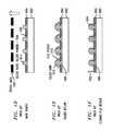
- FIGS. 5B-5Mdepict various exemplary designs of SR openings for forming high volume IMS solder bumps on pads without a mask in the case of SMD (solder mask defined) substrates, according to aspects of the invention.
- FIGS. 5B-5Dare generally similar to FIGS. 4A-4C , with top views depicted at the right side of the figure.
- the openings 5019 in the SRare circular in the top view.
- the openings 5019are funnel-shaped in the side view, with a short straight region 5021 .
- the value of w 1can decide the height of the solder bump over the SR after the solder reflow. It is generally acceptable if there is not any overlap among the neighboring SR openings.
- FIGS. 5E-5Gare similar to FIGS. 5B-5D , but for an embodiment where openings 5023 are “stepped” having small-diameter region 5025 near pad 4006 and large-diameter region 5027 .
- the openings 5023 in the SR with regions 5025 , 5027are circular in the top view.
- the openingscan be sized using principles similar to those above; it is generally acceptable if there is not any overlap among the neighboring SR openings.
- FIGS. 5H-5Jare similar to FIGS. 5B-5D , but for an embodiment where openings 5029 have offset “reservoirs” 5031 .
- the main portions 5033 of the openings 5029 in the SRare circular in the top view.
- the reservoir regions 5031are in fluid communication with the main portions 5033 .
- the openingscan be sized using principles similar to those above; it is generally acceptable if there is not any overlap among the neighboring SR openings.
- FIGS. 5K-5Mare similar to FIGS. 5B-5D , but for an embodiment where openings 5035 have a plurality of offset “reservoirs” 5037 .
- the main portions 5039 of the openings 5035 in the SR, as well as the reservoirs 5037are circular in the top view.
- the reservoir regions 5037are in fluid communication with the main portions 5039 .
- the openingscan be sized using principles similar to those above; it is generally acceptable if there is not any overlap among the neighboring SR openings.
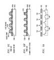
- FIG. 6Ashows a baseline aspect somewhat similar to FIG. 1A for comparison purposes, but wherein the pads 6006 are within large openings 6049 in the SR 6051 , such that portions of the surface of substrate 6002 are visible adjacent pads 6006 .
- NSMDnod solder mask defined
- FIGS. 6B-6Gillustrate various exemplary designs of deep SR openings for forming high volume IMS solder bumps on the pads without a mask in the case of NSMD (non solder mask defined) substrates, according to aspects of the invention.
- openings 6053are larger than pads 6006 , as for openings 6049 in FIG. 6A ; however, a surrounding trench 6055 is formed in the substrate itself.
- the solderhas an adhesion (wetting) with the copper pads but it does not have an adhesion with the solder resist.
- FIGS. 6D and 6Gnote that the solder covers the side wall of the copper pads.
- the trenchis filled with solder 114 , as in FIG. 6C , and due to surface tension, after reflow, the structure depicted in FIG. 6D is obtained, with solder balls 4016 .
- the trenches 6055 and pads 6006are circular in the top views.
- FIGS. 6E-6Gare similar to FIGS. 6B-6D , except that the trenches 6057 do not extend around the complete circumference of the pads 6006 . Purely for example, trenches 6057 extending over half the circumference of the pads 6006 are shown.
- FIGS. 6B-6Dshow three steps of as received, IMS, and reflow
- FIGS. 6E-6Gshows examples of different SR designs.
- the SRdoes not cover the copper pads as in the SMD type.
- FIG. 6Ein the top view, the top of substrate 6002 and the bottom of trench 6057 in substrate 6002 are visible surrounding pads 6006 .
- FIG. 6Fthe entire opening 6049 , including trench 6057 , is filled with solder 114 . Due to surface tension, after reflow, the structure depicted in FIG. 6G is obtained, with solder balls 4016 . The solder is only wetting on the copper pads, but it is not wetting on the SR after the reflow.
- FIG. 6Gin the top view, the top of substrate 6002 and the bottom of trench 6057 in substrate 6002 are again visible.
- solder-receiving volumes for the embodiments of FIGS. 6 and 7can also be sized using similar techniques to those set forth above; overlap among the neighboring SR openings should be avoided. Also, the depth can define the height of the solder bumps over SR after reflow. For any of the embodiments herein, the skilled artisan, given the teachings herein, will be able to perform geometric calculations to size the solder-receiving volumes such that the solder balls or blobs project above the surface of the solder resist at completion.
- the approximate shape of the solder balls or blobswill be known based on the tendency to assume spherical shapes under surface tension, together with knowledge of which surfaces wet and which do not; the solder-receiving volumes are configured and dimensioned to have sufficient volume such that the volume of solder therein, upon reflow or solidification in Nitrogen or forming gas environment, will form a shape of ball or blob that projects as desired.
- the skilled persongiven the teachings herein can easily calculate the relation between the opening volume of SR and the height of solder over SR.
- FIGS. 7A-7Care similar to FIGS. 4A-4C , except that they show a case where the process is carried out in a nitrogen environment 7069 in which the molten solder forms spheres (“balls-up”) before solidification.
- Solder head 112 with compliant portion 116 delivering solder 114can be implemented, for example, as described above.
- nitrogena forming gas environment can be used.
- the forming gasis a mixture of Nitrogen (N 2 ) and Hydrogen (H 2 ); generally, 90% N 2 and 10% H 2 .
- the nitrogen environmentenables the solder to become generally spherical before solidification as at 7071 in FIG. 7C . This leads to a solidified solder bump that is higher than the solder resist surface without an additional solder reflow process.
- a wide SR openingcan help to increase the height of the substrate solder bump.
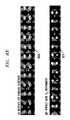
- FIGS. 8A-8Epresent exemplary successful experimental verification of techniques as shown in FIGS. 7A-7C .
- the as-received OSP finished substrate 8081shows the pads 8006 to be below the SR surface.
- “OSP”is Organic Solderability Preservative—OSP is coated on the top of copper pads. OSP provides oxidation resistance and corrosion resistance of copper pads before a solder bump is formed on the copper pads.
- the IMS bumped substrate 8083shows the solder bumps 8071 to be above the SR surface. A 150 micron pitch was employed for experimental purposes. Note that FIG. 8D and FIG. 8E are the same picture, but FIG. 8D is 50 times magnification and FIG. 8E is 100 times magnification.
- one or more embodiments of the inventionintentionally form “wide-open” solder resist openings, as opposed to techniques where angled SR openings may occur naturally but unintentionally during a wet etching process.
- a method of forming high volume solder bumps on a substrateincludes carrying out an injection molded solder process without a mask, and providing a substrate having a plurality of wet-able metal pads in recessed regions.
- the substratehas solder resist openings above the pads that are wider than the metal pads.
- a substratehaving a plurality of wet-able pads in recessed regions and having wide-open solder resists defining volumes.
- Molten solderis directly injected into the volumes with the wet-able pads and the wide open solder resists, such that the volumes with the wet-able pads and the wide open solder resists are filled with solder.
- the solderis allowed to solidify, whereby the solder forms a plurality of solder structures adhered to the wet-able pads but not adhered to the wide open solder resists.
- the solidified solderis reflowed with flux or in a formic acid environment to “spheroid-ize” the solder on the wet-able pads.
- a method of injection molded solder without a mask in a nitrogen (or forming gas) environmentfor forming solder bumps which have a greater height than the solder resist of the laminates.
- a substratehaving a plurality of wet-able pads in recessed regions defining volumes.
- Molten solderis directly injected into the volumes with the wet-able pads in the nitrogen environment, such that the volumes with the wet-able pads are filled with solder.
- the solderis allowed to solidify in the nitrogen environment, whereby the solder forms round top structures adhered to the wet-able pads.
- the solidified solder heightis higher than the solder resist.
- a method for forming solder bumps on a substrate without a maskis provided.
- a substratehas wet-able pads in recessed regions and a wide open solder resist which defines volumes.
- Molten solderis directly injected into the volumes and filled with solder. The solder is allowed to solidify and adhered to the wettable pads but not adhered to the wide open solder resist.
- a following reflow processforms high volume solder bumps on the wettable pads.
- the molten solder injection process and the solidifying of solder in a nitrogen environmentforms “spheroid-ized” solder bumps with a height greater than the solder resist without an additional reflow process.
- One or more embodiments of the inventionmay employ almost any kind of solder, although very high melting temperature solder such as 97Pb3Sn may not be desirable for reasons as set forth below.
- Eutectic SnPb (37Pb63Sn) and Pb-free solder(pure Sn, SnAgCu, SnAg, SnCu, SnBi, SnIn, etc.) are non-limiting examples of suitable solders.
- the melting temperature of 97Pb3Snis 320° C., so the organic substrate could be decomposed if using same, even though the time for molten solder injection is short. Any types of solders which have melting temperatures below 285° C. are believed to be particularly advantageous.
- the temperature of solderis above its melting temperature. Any type of substrates which has recessed pads may be employed.
- the oxygen concentration in the Nitrogen environmentis preferably less than 10,000 ppm.
- the Nitrogendoes not have to be perfectly pure and the forming gas does not have to have the exact composition as described elsewhere, as long as the basic functionality shown in FIGS. 7B and 7C can be obtained.
- an exemplary methodincludes the step (see, e.g., FIGS. 4A , 5 B, 5 E, 5 H, 5 K, 6 B, 6 E) of obtaining an assembly comprising a substrate 4002 , 6002 ; a plurality of wet-able pads 4006 , 6006 formed on a surface of the substrate; and a solder resist layer 4004 , 6051 deposited on the surface of the substrate and having an outer surface (upmost surface in the figures). At least the solder resist layer is formed with recessed regions defining volumes 4019 , 5019 , 5023 , 5029 , 5035 , 6049 adjacent the wet-able pads.
- the methodalso includes (see, e.g., FIGS. 4B , 5 C, 5 F, 5 I, 5 L, 6 C, 6 F) directly injecting molten solder into the volumes adjacent the wet-able pads, such that the volumes adjacent the wet-able pads are filled with solder; and allowing the solder to solidify.
- the solderforms a plurality of solder structures (solder-filled volumes in FIGS. 4B , 5 C, 5 F, 5 I, 5 L, 6 C, 6 F where solder has solidified) adhered to the wet-able pads.
- a further stepincludes re-heating the substrate and the solder after the solidification, to re-flow the solder into generally spherical balls 4016 , extending above the outer surface of the solder resist layer.
- “Generally spherical”means spherical or sphere-like under the action of surface tension, with a possible flattened region adjacent the pad; the solder has a spherical shape due to its surface tension—one side which contacts the wetting pads (copper pad) has flattened shape but the other side which is free has spherical shape.
- the volumes adjacent the wet-able padsare configured and dimensioned to receive sufficient solder in the injecting step such that the generally spherical balls extend above the outer surface of the solder resist layer as a result of the re-heating step.
- the solder ballsextend above the outer surface of the solder resist layer by about 15 microns ⁇ about 45 microns. This range is appropriate for stencil printed solder bumps in a 150 micron pitch substrate. If the pitch of the substrate decreases, the required solder height above SR might be shorter. Therefore, in another aspect, the solder balls extend above the outer surface of the solder resist layer by about 5 microns ⁇ about 45 microns.
- the step of directly injecting the molten solderis carried out with an injection molded solder fill head 112 , and the fill head comprises compliant material 116 interposed between the fill head and the solder resist layer to accommodate topographical features of the solder resist.
- the substratecomprises an organic substrate.
- the step of directly injecting the molten solderis carried out with an injection molded solder fill head 112 , and an additional step includes causing relative motion between (i) the head and (ii) the substrate, during the injecting.
- the substrateis a solder-mask-defined substrate.
- the volumes 4019 , 5019 adjacent the wet-able pads 4019 , 5019are at least partially frustoconical (e.g., frustoconical, or part is frustoconical and part is cylindrical), having smaller diameters adjacent the pads and larger diameters opposite the pads.
- the volumes 5023 adjacent the wet-able padshave a stepped cylindrical configuration, having a smaller diameter cylinder 5025 adjacent the pads and a larger diameter cylinder 5027 opposite the pads.
- the volumes 5029 , 5035 adjacent the wet-able padshave a central cylindrical portion 5033 , 5039 adjacent the pads and at least one peripheral reservoir portion 5031 , 5037 in fluid communication with the central cylindrical portion.
- the volumes adjacent the wet-able padshave at least four of the peripheral reservoir portions 5037 in fluid communication with the central cylindrical portion 5039 .
- the substrateis a non-solder-mask-defined substrate.
- the substrate 6002in the step of obtaining the assembly, is also formed with recessed regions 6055 , 6057 , and the recessed regions of the substrate cooperatively define the volumes 6049 together with the recessed regions of the solder resist layer 6051 .
- the recessed regions 6055 , 6057 of the substratecomprise trenches extending at least partially about the pads (partial in FIGS. 6E-6G , completely surrounding in FIGS. 6B-6D ).
- another exemplary methodincludes the step (see FIG. 7A ) of obtaining an assembly comprising a substrate 7002 ; a plurality of wet-able pads 7006 formed on a surface of the substrate; and a solder resist layer 7004 deposited on the surface of the substrate and having an outer surface. At least the solder resist layer is formed with recessed regions (not separately numbered—voides over pads 7006 ) defining volumes adjacent the wet-able pads.
- An additional stepincludes directly injecting molten solder 114 into the volumes adjacent the wet-able pads, such that the volumes adjacent the wet-able pads are filled with solder.
- the injectingis carried out in one of a nitrogen environment and a forming gas environment, as per 7069 .
- An additional stepincludes allowing the solder to solidify, whereby the solder forms a plurality of at least partially spherical solder structures 7071 adhered to the wet-able pads.
- the solidificationis carried out in the aforementioned nitrogen or forming gas environment, as seen in FIG. 7C .
- the volumes adjacent the wet-able padsare configured and dimensioned to receive sufficient solder in the injecting step such that the generally spherical solder structures 7071 extend above the outer surface of the solder resist layer as a result of the solidification step.
- the solder balls 7071extend above the outer surface of the solder resist layer by about 15 microns ⁇ about 45 microns. This range is appropriate for stencil printed solder bumps in a 150 micron pitch substrate. If the pitch of the substrate decreases, the required solder height above SR might be shorter. Therefore, in another aspect, the solder balls extend above the outer surface of the solder resist layer by about 5 microns ⁇ about 45 microns.
- the step of directly injecting the molten solder 114can be carried out with an injection molded solder fill head 112 .
- the fill headcan include compliant material 116 interposed between the fill head and the solder resist layer to accommodate topographical features of the solder resist 7004 .
- the substrateis an organic substrate.
- the step of directly injecting the molten solderis carried out with an injection molded solder fill head 112 , and an additional step includes causing relative motion between (i) the head and (ii) the substrate, during the injecting.
- the methods described abovecan be used in the fabrication and packaging of integrated circuit chips; in particular, techniques set forth herein can be used to make arrays of solder balls for attachment to an integrated circuit chip.
- the chip designcan be created, for example, in a graphical computer programming language, and stored in a computer storage medium (such as a disk, tape, physical hard drive, or virtual hard drive such as in a storage access network). If the designer does not fabricate chips or the photolithographic masks used to fabricate chips, the designer may transmit the resulting design by physical means (e.g., by providing a copy of the storage medium storing the design) or electronically (e.g., through the Internet) to such entities, directly or indirectly.
- physical meanse.g., by providing a copy of the storage medium storing the design
- electronicallye.g., through the Internet
- the stored designcan then be converted into an appropriate format such as, for example, Graphic Design System II (GDSII), for the fabrication of photolithographic masks, which typically include multiple copies of the chip design in question that are to be formed on a wafer.
- GDSIIGraphic Design System II
- the photolithographic maskscan be utilized to define areas of the wafer (and/or the layers thereon) to be etched or otherwise processed.
- Resulting integrated circuit chipscan be distributed by the fabricator in raw wafer form (that is, as a single wafer that has multiple unpackaged chips), as a bare die or in a packaged form.
- the chipcan be mounted in a single chip package (such as a plastic carrier, with leads that are affixed to a mother board or other higher level carrier) or in a multi-chip package (such as a ceramic carrier that has either or both surface interconnections or buried interconnections).
- the chipmay then be integrated with other chips, discrete circuit elements and/or other signal processing devices as part of either (a) an intermediate product, such as a mother board, or (b) an end product.
- the end productcan be any product that includes integrated circuit chips, ranging from toys and other low-end or consumer electronic applications to advanced computer products, having a display, a keyboard or other input device, and a central processor.
- the techniques set for the hereincan be used for interconnecting the chip on chips or chip stacks for 3D applications, chips on wafers, chips on package or package on package.
Landscapes
- Engineering & Computer Science (AREA)
- Microelectronics & Electronic Packaging (AREA)
- Computer Hardware Design (AREA)
- Power Engineering (AREA)
- Manufacturing & Machinery (AREA)
- Physics & Mathematics (AREA)
- Condensed Matter Physics & Semiconductors (AREA)
- General Physics & Mathematics (AREA)
- Ceramic Engineering (AREA)
- Electric Connection Of Electric Components To Printed Circuits (AREA)
- Wire Bonding (AREA)
Abstract
Description
- The present invention generally relates to the electrical and electronic arts and, more particularly, to injection molded solder techniques, solder mask design methods, and solder deposition on substrates.
- J-W Nah et al., ‘A Study on Coining Processes of Solder Bumps on Organic Substrates,’ IEEE Transactions on electronics packaging manufacturing, Vol. 26, No. 2, April 2003, p. 166, shows a current high volume manufacturing method of forming solder bumps on laminates. The solder paste stencil printing method has been used for forming solder bumps on organic substrates for a long time. As seen in
FIGS. 1A and 1B , anorganic substrate 1002 is provided with a plurality ofpads 1006 and asolder resist layer 1004. Astencil mask 1008 is aligned therewith. As inFIG. 1C ,solder paste 1012 is dispensed through the holes inmask 1008 using a squeeze knife orblade 1010. The mask is removed as inFIG. 1D leaving upstandingsolder paste regions 1014.FIG. 1E depicts reflow whereinregions 1014 becomerounded bumps 1016 withflux residue 1018 thereon. The same is cleaned away inFIG. 1F leavingsolder balls 1016 with a projecting height above the resist shown at1020. FIGS. 1A-1F thus illustrate a prior-art technique for forming solder bumps on substrates. Solder paste is stencil printed through a mask aligned to the substrate solder resist (SR) openings. The mask enables deposition of solder paste material that stands above the SR after mask removal.- However, commercial applications of the solder paste stencil printing method are limited to substrates with pitches greater than or equal to 150 microns because the high volume percentage of flux (around 50 volume %) in the solder paste hinders formation of high volume solder bumps without solder bridging.
- U.S. Pat. No. 6,213,386 of Inoue et al., entitled ‘Method of forming bumps,’ discloses wherein solder balls and a tool having a large number of through-holes are used, and under the condition that the through-holes of the tool are aligned with the pads of the semiconductor device, the solder balls are charged into the through-holes, pressed to be fixed on the pads, and then reflowed to form bumps.
FIGS. 2A-2H illustrate a prior-art pre-formed solder ball mounting method for fine pitch applications under 150 microns pitch. Elements similar to those inFIGS. 1A-1F have received the same reference character. As seen inFIG. 2A , anorganic substrate 1002 is provided with a plurality ofpads 1006 and asolder resist layer 1004. A mask forflux 2020 is aligned therewith. As inFIG. 2B ,tacky flux 2002 is applied, and as inFIG. 2C ,mask 2020 withadherent flux 2002 is removed, leavingflux portions 2004 onpads 1006. Amask 2006 for solder ball dispensing is aligned with the pads, as inFIG. 2D , and inFIG. 2E , preformedsolder balls 2008 are located in openings in themask 2006, in contact withflux portions 2004, which retain them when themask 2006 is removed as inFIG. 2F .FIGS. 2G and 2H depict reflow and flux cleansing and are similar toFIGS. 1E and 1F .FIGS. 2A-2H thus illustrate another prior-art technique for forming solder bumps on substrates; the so-called micro ball mounting method wherein two masks are used: one to dispense tacky flux and the other to place preformed solder balls on the pads of the substrate. The tacky flux makes the balls stick to the bottom of the SR opening.Solder balls 2008 may be expensive and flux application and solder ball dispensing may be somewhat complex. Furthermore, this type of technology needs additional steps to form uniform height solder bumps on different size pads.- Principles of the present invention provide techniques for direct IMS (injection molded solder) without a mask for forming solder bumps on substrates. An exemplary method includes the step of obtaining an assembly comprising a substrate; a plurality of wet-able pads formed on a surface of the substrate; and a solder resist layer deposited on the surface of the substrate and having an outer surface. At least the solder resist layer is formed with recessed regions defining volumes adjacent the wet-able pads. The method also includes directly injecting molten solder into the volumes adjacent the wet-able pads, such that the volumes adjacent the wet-able pads are filled with solder; allowing the solder to solidify, whereby the solder forms a plurality of solder structures adhered to the wet-able pads; and re-heating the substrate and the solder after the solidification, to re-flow the solder into generally spherical balls extending above the outer surface of the solder resist layer. The volumes adjacent the wet-able pads are configured and dimensioned to receive sufficient solder in the injecting step such that the generally spherical balls extend above the outer surface of the solder resist layer as a result of the re-heating step.
- In another aspect, another exemplary method includes the step of obtaining an assembly comprising a substrate; a plurality of wet-able pads formed on a surface of the substrate; and a solder resist layer deposited on the surface of the substrate and having an outer surface. At least the solder resist layer is formed with recessed regions defining volumes adjacent the wet-able pads. Additional steps include directly injecting molten solder into the volumes adjacent the wet-able pads, such that the volumes adjacent the wet-able pads are filled with solder, the injecting being carried out in one of a nitrogen environment and a forming gas environment; and allowing the solder to solidify, whereby the solder forms a plurality of at least partially spherical solder structures adhered to the wet-able pads, the solidification being carried out in the one of the nitrogen environment and the forming gas environment. The volumes adjacent the wet-able pads are configured and dimensioned to receive sufficient solder in the injecting step such that the generally spherical solder structures extend above the outer surface of the solder resist layer as a result of the solidification step.
- These and other objects, features and advantages of the present invention will become apparent from the following detailed description of illustrative embodiments thereof, which is to be read in connection with the accompanying drawings (note that section lining is generally omitted from the drawings, except with respect to
mask 102 inFIGS. 3A-3D , in order to avoid clutter). FIGS. 1A-1F schematically depict a prior-art solder paste stencil method (a high volume manufacturing method for forming solder bumps on substrates);FIGS. 2A-2H schematically depict a prior-art micro ball mounting method for forming solder bumps on substrates;FIGS. 3A-3F schematically depict a substrate IMS with mask process of U.S. patent application Ser. No. 12/269,240;FIGS. 4A-4C schematically depict, at a high level, an exemplary direct substrate IMS process without mask, according to an aspect of the invention;FIGS. 5A-5M schematically depict an exemplary direct substrate IMS process without mask exercised with an SMD (solder mask defined) substrate having wide-open SR, according to another aspect of the invention (with a baseline for comparison);FIGS. 6A-6G schematically depict an exemplary direct substrate IMS process without mask exercised with an NSMD (non solder mask defined) substrate having a deep SR opening, according to still another aspect of the invention (with a baseline for comparison);FIGS. 7A-7C schematically depict a direct substrate IMS process without mask (exercised in a nitrogen environment) according to a further aspect of the invention; andFIGS. 8A-8E schematically depictdirect substrate IMS without mask, on a laminate having the industry standard SR opening.- Initially, the complete disclosure of U.S. patent application Ser. No. 12/269,240 of Gruber et al., filed Nov. 12, 2008, entitled “Injection Molded Solder Method for Forming Solder Bumps on Substrates” (“the '240 application”) is expressly incorporated herein by reference in its entirety for all purposes.
FIGS. 3A-3F depict certain techniques of the '240 application. Attention should now be given toFIGS. 3A and 3B . As seen therein, amask 102 includes a plurality of throughholes 104 arranged in a desired pattern. Themask 104 is located adjacent asubstrate 106. The substrate may be, for example, an organic substrate with a plurality of wet-able pads108 (for example, copper, gold, nickel, and the like) located in recesses. The mask may be, for example, a polyimide film or a thin material that does not react with solder (e.g., non-wetting metals such as molybdenum, stainless steel, aluminum, and the like). As shown inFIG. 3A , themask 102 is aligned to thesubstrate 106 so thatholes 104 align withpads 108. Note that holes104 are preferably not of uniform diameter, but rather frustoconical, with the larger diameteradjacent substrate 106 as seen inFIG. 3B . The assembly inFIG. 3B is ready to receive solder. - Non-limiting examples of organic substrates include laminate materials made of glass fibers in an epoxy; for example, FR-4 (flame retardant type 4) and BT-resin (Bismaleimide Triazine resin). Furthermore, it should be noted that techniques of the '240 application are not limited to organic substrates;
element 106 is also representative of a silicon wafer, as aspects of the '240 application can also be employed to create solder bumps on silicon wafers. Thus, the wet-able pads 108 depicted in the figures represent wet-able pads and also encompass ball-limiting metallurgy, in the case of a silicon substrate. - A solder fill process is shown in
FIG. 3C , whereinfill head 112 dispensessolder 114 into theholes 104 and the recessed regions with pads of wet-able material 108 to formsolder structures 110. As best seen inFIG. 3C , the recessed regions may be such that the top surface of the pads of wet-able material is recessed below the top surface of thesubstrate 106 by a distance X of about 5-15 microns. This results in a “shoulder” of solder material.Fill head 112 is provided withcompliant material 116 for purposes to be discussed below. As seen inFIGS. 3D and 3E , after solder solidification, the mask102 (also referred to herein as a “decal” or “decal layer”) is peeled away onto areel 118 with the aid of a peel roller3004 (peelroller 3004 may be provided to aid in peelingmask 102 from substrates106). Becauseholes 104 are frustoconical with the wide side towardssubstrate 106, they are not re-entrant, anddecal 102 peels relatively easily, without undue mechanical stress onstructures 110 orsubstrate 106. Optionally, as seen inFIG. 3F , a reflow process is conducted such thatsolder structures 110 become substantially hemispherical solder bumps120. - With regard to
compliant material 116, note thatsubstrate 106 may be formed, for example, from a base substrate with solder resist (SR). Wet-able pads (e.g., copper) are shown at108. The upper surface of the solder resist is not perfectly flat, but includes topographical features. These will prevent a perfect seal withdecal mask 102, thus resulting in a small gap with concomitant leakage of solder during the IMS process.Fill head 112, which may be, for example, glass or metal, is provided withcompliant material 116, which spreads out (distributes uniformly, or nearly so) the compressive force between (i)head 112 and (ii)decal 102 onsubstrate 106, resulting in good contact betweenmask 102 andsubstrate 106, such that gaps that would cause undesirable leakage are reduced or eliminated. Themask 102 is sufficiently flexible to track the topography of thesubstrate 106, under the influence of the compressive force that is distributed bycompliant material 116. Compliant material 116 may include, for example, a bulk compressible layer with a thin low-friction layeradjacent mask 102. Non-limiting examples of compliant materials for the bulk compressible layer are silicone rubber and silicone closed cell sponge. Non-limiting examples of materials for the low-friction layer are fluoropolymers such as Teflon® (registered mark of E. I. Du Pont De Nemours And Company, Wilmington, Del., USA) and Rulon® TFE Fluorocarbon (registered mark of Saint-Gobain Performance Plastics Corporation, Aurora, Ohio USA). The low-friction layer may be just thick enough to resist abrasion, for example. The total thickness of the low friction layer plus the bulk compressible layer may be, for example, from about 1/32 inch to about ¼ inch, with a preferred thickness of about 1/16 inch (from about 0.79 mm to about 6.35 mm, with a preferred thickness of about 1.59 mm). The contact pressure may be about 10 to about 60 pounds per square inch (PSI) with a preferred value of about 15 PSI (about 68.9 to about 414 kilo-Pascals with a preferred value of about 103 kilo-Pascals).FIGS. 3A-3F thus illustrate injection of molten solder with a mask process. Solder bumps are formed on the pads of the substrate with the mask ensuring enough solder volume above the SR surface. The direct injection of molten solder with a flexible mask has demonstrated 80 micron pitch solder bumping on a substrate. Such techniques advantageously provide simple molten solder injection with a flexible film mask for forming high volume solder bumps on very fine pitch laminates which have less than 80 micron pitch. Embodiments of such method may use a mask which requires an alignment step between the film mask and the laminate when the industry standard panel sized substrate is used.- One or more embodiments of the present invention provide a method for forming solder bumps on organic substrates by using direct IMS on substrates without a mask. By manipulation of the opening in the solder resist (SR) it is possible to enable variations in the volume of solder bumps. Therefore, there is no issue with alignment between holes in a mask and pads on a substrate. Since mask alignment is a time-consuming process step, the elimination of this step lowers process cost and makes the process more reliable.
- In another aspect, an SR opening that is wider than the wet-able metal pad is fabricated. This opening can accept a larger volume of injected solder material than a standard SR pad opening. During the subsequent reflow process the solder moves from the non-wetting, pure SR area to the wet-able metal area. Therefore, a higher volume solder bump which has a height above the SR surface can be achieved.
- In some instances, a nitrogen environment during the IMS process serves to make the solder “ball-up” during the solidification of the injected molten solder. Thus, the presence of a nitrogen environment has the potential to eliminate the subsequent reflow process typically used in other cases. This reduces the number of process steps and thus cost.
- The solder paste of certain prior-art processes leads to SR openings which are only about 50% volume filled by solder since the solder paste includes about 50 volume percent solder powder and about 50 volume percent flux. After reflow of this solder paste, only about 50 volume percent of the solder paste remains to make the solder bump in the SR opening over the solder pad. To raise the solder volume, a fill process mask has heretofore been a requirement. The mask adds volume to the SR opening and must be thick enough to raise the solder remaining after reflow above the SR surface.
- For the avoidance of doubt, note that in the '240 application, a base substrate with solder resist (SR) is referred to as a substrate; however, in the remainder of this application, the base substrate is referred to simply as a substrate, for brevity.
FIGS. 4A-4C schematically depict, at a high level, an exemplary direct substrate IMS process without mask, according to an aspect of the invention. Noteorganic substrate 4002 withpads 4006 andSR 4004. In the exemplary method for forming solder bumps, enough solder volume is provided above the SR surface by direct IMS. This is achieved by proper design of theSR opening 4019. The “wide open” SR allows a greater volume of molten solder to be injected on the pads. The subsequent solder reflow process makesspherical solder bumps 4016 which protrude above the SR surface sufficiently to ensure good flip chip assembly yield, as shown at4021.- The process shown in
FIGS. 4A-4C is simple, and does not require a mask or an alignment step. Anysize substrate 4002 can be used, up to and including a panel size. As seen inFIG. 4A , the top surface of the SR may project a height h above the top of thepads 4006. The diameter of the “wide open” SR at the bottom,adjacent pads 4006 is designated as w2, while the diameter of the “wide open” SR at the top is designated as w1. The angle with the vertical is designated as a. - The value of h, by way of example and not limitation, may be between 5 microns and 25 microns. The value depends on the application and/or the pitch of the substrates. The value of w2depends on the pitch of the substrates. For example, a 200 microns pitch substrate has around 100 microns diameter w2and a 150 microns pitch substrate has around 80 microns diameter w2. The value of w1can decide the height of the solder bump over the SR after the solder reflow. If the pitch is defined as p (as in
FIG. 4A ), a workable range, in one or more embodiments, is w1<w2<p. - The IMS process is shown in
FIG. 4B . The above-describedhead 112 withcompliant material 116 may be used to dispensesolder 114, in a non-limiting example. InFIG. 4C , solder reflow is carried out with flux or in a formic acid environment, yieldingsolder balls 4016. FIGS. 4D-4F are similar toFIGS. 4A-4C , but show a case where pads of different size are used, resulting in different sizes and/or shapes ofsolder balls 4016.FIG. 5A shows a baseline similar toFIG. 1A for comparison purposes. Refer, for example, to US Patent Publication 2009-0146316.FIGS. 5B-5M depict various exemplary designs of SR openings for forming high volume IMS solder bumps on pads without a mask in the case of SMD (solder mask defined) substrates, according to aspects of the invention.FIGS. 5B-5D are generally similar toFIGS. 4A-4C , with top views depicted at the right side of the figure. Theopenings 5019 in the SR are circular in the top view. Furthermore, theopenings 5019 are funnel-shaped in the side view, with a shortstraight region 5021.- In
FIGS. 5B-5D , as above, the value of w1can decide the height of the solder bump over the SR after the solder reflow. It is generally acceptable if there is not any overlap among the neighboring SR openings. FIGS. 5E-5G are similar toFIGS. 5B-5D , but for an embodiment whereopenings 5023 are “stepped” having small-diameter region 5025 nearpad 4006 and large-diameter region 5027. Theopenings 5023 in the SR withregions FIGS. 5H-5J are similar toFIGS. 5B-5D , but for an embodiment whereopenings 5029 have offset “reservoirs”5031. Themain portions 5033 of theopenings 5029 in the SR are circular in the top view. Thereservoir regions 5031 are in fluid communication with themain portions 5033. The openings can be sized using principles similar to those above; it is generally acceptable if there is not any overlap among the neighboring SR openings.FIGS. 5K-5M are similar toFIGS. 5B-5D , but for an embodiment whereopenings 5035 have a plurality of offset “reservoirs”5037. Themain portions 5039 of theopenings 5035 in the SR, as well as thereservoirs 5037, are circular in the top view. Thereservoir regions 5037 are in fluid communication with themain portions 5039. The openings can be sized using principles similar to those above; it is generally acceptable if there is not any overlap among the neighboring SR openings.FIG. 6A shows a baseline aspect somewhat similar toFIG. 1A for comparison purposes, but wherein thepads 6006 are withinlarge openings 6049 in theSR 6051, such that portions of the surface ofsubstrate 6002 are visibleadjacent pads 6006. Refer, for example, to US Patent Publication 2009-0184419, which is one example of NSMD (nod solder mask defined) substrates. ‘Non-solder-mask-defined’ means that thecopper pads 6006 of the substrates are not covered by the solder resist6049. ‘SMD (solder mask defined)’ means that the copper pads are covered by the solder resist.FIGS. 6B-6G illustrate various exemplary designs of deep SR openings for forming high volume IMS solder bumps on the pads without a mask in the case of NSMD (non solder mask defined) substrates, according to aspects of the invention. InFIGS. 6B-6D ,openings 6053 are larger thanpads 6006, as foropenings 6049 inFIG. 6A ; however, a surroundingtrench 6055 is formed in the substrate itself. The solder has an adhesion (wetting) with the copper pads but it does not have an adhesion with the solder resist. InFIGS. 6D and 6G , note that the solder covers the side wall of the copper pads. The trench is filled withsolder 114, as inFIG. 6C , and due to surface tension, after reflow, the structure depicted inFIG. 6D is obtained, withsolder balls 4016. Thetrenches 6055 andpads 6006 are circular in the top views.FIGS. 6E-6G are similar toFIGS. 6B-6D , except that thetrenches 6057 do not extend around the complete circumference of thepads 6006. Purely for example,trenches 6057 extending over half the circumference of thepads 6006 are shown.- Note
FIGS. 6B-6D show three steps of as received, IMS, and reflow, whileFIGS. 6E-6G shows examples of different SR designs. As far as an “NSMD type substrate,” in the NSMD case, the SR does not cover the copper pads as in the SMD type. - In
FIG. 6E , in the top view, the top ofsubstrate 6002 and the bottom oftrench 6057 insubstrate 6002 are visible surroundingpads 6006. InFIG. 6F , theentire opening 6049, includingtrench 6057, is filled withsolder 114. Due to surface tension, after reflow, the structure depicted inFIG. 6G is obtained, withsolder balls 4016. The solder is only wetting on the copper pads, but it is not wetting on the SR after the reflow. InFIG. 6G , in the top view, the top ofsubstrate 6002 and the bottom oftrench 6057 insubstrate 6002 are again visible. - Note that the solder-receiving volumes for the embodiments of
FIGS. 6 and 7 can also be sized using similar techniques to those set forth above; overlap among the neighboring SR openings should be avoided. Also, the depth can define the height of the solder bumps over SR after reflow. For any of the embodiments herein, the skilled artisan, given the teachings herein, will be able to perform geometric calculations to size the solder-receiving volumes such that the solder balls or blobs project above the surface of the solder resist at completion. For example, the approximate shape of the solder balls or blobs will be known based on the tendency to assume spherical shapes under surface tension, together with knowledge of which surfaces wet and which do not; the solder-receiving volumes are configured and dimensioned to have sufficient volume such that the volume of solder therein, upon reflow or solidification in Nitrogen or forming gas environment, will form a shape of ball or blob that projects as desired. Thus, the skilled person, given the teachings herein can easily calculate the relation between the opening volume of SR and the height of solder over SR. FIGS. 7A-7C are similar toFIGS. 4A-4C , except that they show a case where the process is carried out in anitrogen environment 7069 in which the molten solder forms spheres (“balls-up”) before solidification. Notesubstrate 7002,SR 7004, and generally straight-walled cylindrical openings inSR 7004 nearpads 7006.Solder head 112 withcompliant portion 116 deliveringsolder 114 can be implemented, for example, as described above. Instead of nitrogen a forming gas environment can be used. The forming gas is a mixture of Nitrogen (N2) and Hydrogen (H2); generally, 90% N2and 10% H2. The nitrogen environment enables the solder to become generally spherical before solidification as at7071 inFIG. 7C . This leads to a solidified solder bump that is higher than the solder resist surface without an additional solder reflow process. A wide SR opening can help to increase the height of the substrate solder bump.FIGS. 8A-8E present exemplary successful experimental verification of techniques as shown inFIGS. 7A-7C . The as-received OSP finishedsubstrate 8081 shows thepads 8006 to be below the SR surface. “OSP” is Organic Solderability Preservative—OSP is coated on the top of copper pads. OSP provides oxidation resistance and corrosion resistance of copper pads before a solder bump is formed on the copper pads. The IMS bumpedsubstrate 8083 shows the solder bumps8071 to be above the SR surface. A 150 micron pitch was employed for experimental purposes. Note thatFIG. 8D andFIG. 8E are the same picture, butFIG. 8D is 50 times magnification andFIG. 8E is 100 times magnification.- It should be noted that one or more embodiments of the invention intentionally form “wide-open” solder resist openings, as opposed to techniques where angled SR openings may occur naturally but unintentionally during a wet etching process.
- In one aspect, a method of forming high volume solder bumps on a substrate includes carrying out an injection molded solder process without a mask, and providing a substrate having a plurality of wet-able metal pads in recessed regions. The substrate has solder resist openings above the pads that are wider than the metal pads.
- In some cases, a substrate is obtained, having a plurality of wet-able pads in recessed regions and having wide-open solder resists defining volumes. Molten solder is directly injected into the volumes with the wet-able pads and the wide open solder resists, such that the volumes with the wet-able pads and the wide open solder resists are filled with solder. The solder is allowed to solidify, whereby the solder forms a plurality of solder structures adhered to the wet-able pads but not adhered to the wide open solder resists. The solidified solder is reflowed with flux or in a formic acid environment to “spheroid-ize” the solder on the wet-able pads.
- In another aspect, a method of injection molded solder without a mask in a nitrogen (or forming gas) environment is provided, for forming solder bumps which have a greater height than the solder resist of the laminates.
- In some cases, a substrate is obtained, having a plurality of wet-able pads in recessed regions defining volumes. Molten solder is directly injected into the volumes with the wet-able pads in the nitrogen environment, such that the volumes with the wet-able pads are filled with solder. The solder is allowed to solidify in the nitrogen environment, whereby the solder forms round top structures adhered to the wet-able pads. The solidified solder height is higher than the solder resist.
- In one or more instances, a method for forming solder bumps on a substrate without a mask is provided. A substrate has wet-able pads in recessed regions and a wide open solder resist which defines volumes. Molten solder is directly injected into the volumes and filled with solder. The solder is allowed to solidify and adhered to the wettable pads but not adhered to the wide open solder resist. A following reflow process forms high volume solder bumps on the wettable pads. In addition, the molten solder injection process and the solidifying of solder in a nitrogen environment forms “spheroid-ized” solder bumps with a height greater than the solder resist without an additional reflow process.
- One or more embodiments of the invention may employ almost any kind of solder, although very high melting temperature solder such as 97Pb3Sn may not be desirable for reasons as set forth below. Eutectic SnPb (37Pb63Sn) and Pb-free solder (pure Sn, SnAgCu, SnAg, SnCu, SnBi, SnIn, etc.) are non-limiting examples of suitable solders. The melting temperature of 97Pb3Sn is 320° C., so the organic substrate could be decomposed if using same, even though the time for molten solder injection is short. Any types of solders which have melting temperatures below 285° C. are believed to be particularly advantageous. When the solder is injected, the temperature of solder is above its melting temperature. Any type of substrates which has recessed pads may be employed. The oxygen concentration in the Nitrogen environment is preferably less than 10,000 ppm. The Nitrogen does not have to be perfectly pure and the forming gas does not have to have the exact composition as described elsewhere, as long as the basic functionality shown in
FIGS. 7B and 7C can be obtained. - Given the discussion thus far, it will be appreciated that, in general terms, an exemplary method, according to an aspect of the invention, includes the step (see, e.g.,
FIGS. 4A ,5B,5E,5H,5K,6B,6E) of obtaining an assembly comprising asubstrate able pads layer regions defining volumes FIGS. 4B ,5C,5F,5I,5L,6C,6F) directly injecting molten solder into the volumes adjacent the wet-able pads, such that the volumes adjacent the wet-able pads are filled with solder; and allowing the solder to solidify. The solder forms a plurality of solder structures (solder-filled volumes inFIGS. 4B ,5C,5F,5I,5L,6C,6F where solder has solidified) adhered to the wet-able pads. With reference toFIGS. 4C ,5D,5G,5J,5M,6D,6G, a further step includes re-heating the substrate and the solder after the solidification, to re-flow the solder into generallyspherical balls 4016, extending above the outer surface of the solder resist layer. “Generally spherical” means spherical or sphere-like under the action of surface tension, with a possible flattened region adjacent the pad; the solder has a spherical shape due to its surface tension—one side which contacts the wetting pads (copper pad) has flattened shape but the other side which is free has spherical shape. - The volumes adjacent the wet-able pads are configured and dimensioned to receive sufficient solder in the injecting step such that the generally spherical balls extend above the outer surface of the solder resist layer as a result of the re-heating step.
- As seen, for example, at4021, in some cases, the solder balls extend above the outer surface of the solder resist layer by about 15 microns˜about 45 microns. This range is appropriate for stencil printed solder bumps in a 150 micron pitch substrate. If the pitch of the substrate decreases, the required solder height above SR might be shorter. Therefore, in another aspect, the solder balls extend above the outer surface of the solder resist layer by about 5 microns˜about 45 microns.
- In some instances, the step of directly injecting the molten solder is carried out with an injection molded
solder fill head 112, and the fill head comprisescompliant material 116 interposed between the fill head and the solder resist layer to accommodate topographical features of the solder resist. - In at least some instances, the substrate comprises an organic substrate.
- In one or more embodiments, the step of directly injecting the molten solder is carried out with an injection molded
solder fill head 112, and an additional step includes causing relative motion between (i) the head and (ii) the substrate, during the injecting. - In some instances, in the step of obtaining the assembly, the substrate is a solder-mask-defined substrate.
- As seen in
FIGS. 4A-4F and5B-5D, in some cases, in the step of obtaining the assembly, thevolumes able pads - As seen in
FIGS. 5E-5G , in some cases, in the step of obtaining the assembly, thevolumes 5023 adjacent the wet-able pads have a stepped cylindrical configuration, having asmaller diameter cylinder 5025 adjacent the pads and alarger diameter cylinder 5027 opposite the pads. - As seen in
FIGS. 5H-5M , in some cases, in the step of obtaining the assembly, thevolumes cylindrical portion peripheral reservoir portion - As in
FIGS. 5K-5M , in some cases, in the step of obtaining the assembly, the volumes adjacent the wet-able pads have at least four of theperipheral reservoir portions 5037 in fluid communication with the centralcylindrical portion 5039. - In some instances, in the step of obtaining the assembly, the substrate is a non-solder-mask-defined substrate.
- In some cases, such as in
FIGS. 6B-6G , in the step of obtaining the assembly, thesubstrate 6002 is also formed with recessedregions volumes 6049 together with the recessed regions of the solder resistlayer 6051. - As shown in the example of
FIGS. 6B-6G , in some cases, in the step of obtaining the assembly, the recessedregions FIGS. 6E-6G , completely surrounding inFIGS. 6B-6D ). - Furthermore, given the discussion thus far, it will be appreciated that, in general terms, another exemplary method, according to another aspect of the invention, includes the step (see
FIG. 7A ) of obtaining an assembly comprising asubstrate 7002; a plurality of wet-able pads 7006 formed on a surface of the substrate; and a solder resistlayer 7004 deposited on the surface of the substrate and having an outer surface. At least the solder resist layer is formed with recessed regions (not separately numbered—voides over pads7006) defining volumes adjacent the wet-able pads. An additional step (seeFIG. 7B ) includes directly injectingmolten solder 114 into the volumes adjacent the wet-able pads, such that the volumes adjacent the wet-able pads are filled with solder. The injecting is carried out in one of a nitrogen environment and a forming gas environment, as per7069. An additional step includes allowing the solder to solidify, whereby the solder forms a plurality of at least partiallyspherical solder structures 7071 adhered to the wet-able pads. The solidification is carried out in the aforementioned nitrogen or forming gas environment, as seen inFIG. 7C . The volumes adjacent the wet-able pads are configured and dimensioned to receive sufficient solder in the injecting step such that the generallyspherical solder structures 7071 extend above the outer surface of the solder resist layer as a result of the solidification step. - In some instances, as a result of the solidification step, the
solder balls 7071 extend above the outer surface of the solder resist layer by about 15 microns˜about 45 microns. This range is appropriate for stencil printed solder bumps in a 150 micron pitch substrate. If the pitch of the substrate decreases, the required solder height above SR might be shorter. Therefore, in another aspect, the solder balls extend above the outer surface of the solder resist layer by about 5 microns˜about 45 microns. - The step of directly injecting the
molten solder 114 can be carried out with an injection moldedsolder fill head 112. The fill head can includecompliant material 116 interposed between the fill head and the solder resist layer to accommodate topographical features of the solder resist7004. - In at least some instances, the substrate is an organic substrate.
- In one or more embodiments, the step of directly injecting the molten solder is carried out with an injection molded
solder fill head 112, and an additional step includes causing relative motion between (i) the head and (ii) the substrate, during the injecting. - The methods described above can be used in the fabrication and packaging of integrated circuit chips; in particular, techniques set forth herein can be used to make arrays of solder balls for attachment to an integrated circuit chip. The chip design can be created, for example, in a graphical computer programming language, and stored in a computer storage medium (such as a disk, tape, physical hard drive, or virtual hard drive such as in a storage access network). If the designer does not fabricate chips or the photolithographic masks used to fabricate chips, the designer may transmit the resulting design by physical means (e.g., by providing a copy of the storage medium storing the design) or electronically (e.g., through the Internet) to such entities, directly or indirectly. The stored design can then be converted into an appropriate format such as, for example, Graphic Design System II (GDSII), for the fabrication of photolithographic masks, which typically include multiple copies of the chip design in question that are to be formed on a wafer. The photolithographic masks can be utilized to define areas of the wafer (and/or the layers thereon) to be etched or otherwise processed.
- Resulting integrated circuit chips can be distributed by the fabricator in raw wafer form (that is, as a single wafer that has multiple unpackaged chips), as a bare die or in a packaged form. In the latter case, the chip can be mounted in a single chip package (such as a plastic carrier, with leads that are affixed to a mother board or other higher level carrier) or in a multi-chip package (such as a ceramic carrier that has either or both surface interconnections or buried interconnections). In any case, the chip may then be integrated with other chips, discrete circuit elements and/or other signal processing devices as part of either (a) an intermediate product, such as a mother board, or (b) an end product. The end product can be any product that includes integrated circuit chips, ranging from toys and other low-end or consumer electronic applications to advanced computer products, having a display, a keyboard or other input device, and a central processor. The techniques set for the herein can be used for interconnecting the chip on chips or chip stacks for 3D applications, chips on wafers, chips on package or package on package.
- It will be appreciated and should be understood that the exemplary embodiments of the invention described above can be implemented in a number of different fashions. Given the teachings of the invention provided herein, one of ordinary skill in the related art will be able to contemplate other implementations of the invention.
- Although illustrative embodiments of the present invention have been described herein with reference to the accompanying drawings, it is to be understood that the invention is not limited to those precise embodiments, and that various other changes and modifications may be made by one skilled in the art without departing from the scope or spirit of the invention.
Claims (19)
Priority Applications (4)
| Application Number | Priority Date | Filing Date | Title |
|---|---|---|---|
| US12/706,212US8492262B2 (en) | 2010-02-16 | 2010-02-16 | Direct IMS (injection molded solder) without a mask for forming solder bumps on substrates |
| JP2012552885AJP5753544B2 (en) | 2010-02-16 | 2011-01-19 | Direct IMS (injection molding solder) without using a mask to form solder bumps on the substrate |
| PCT/US2011/021626WO2011102929A2 (en) | 2010-02-16 | 2011-01-19 | Direct ims (injection molded solder) without a mask for formaing solder bumps on substrates |
| GB1214867.2AGB2491739B (en) | 2010-02-16 | 2011-01-19 | Direct IMS (Injection Molded Solder) without mask for forming solder bumps on substrates |
Applications Claiming Priority (1)
| Application Number | Priority Date | Filing Date | Title |
|---|---|---|---|
| US12/706,212US8492262B2 (en) | 2010-02-16 | 2010-02-16 | Direct IMS (injection molded solder) without a mask for forming solder bumps on substrates |
Publications (2)
| Publication Number | Publication Date |
|---|---|
| US20110201194A1true US20110201194A1 (en) | 2011-08-18 |
| US8492262B2 US8492262B2 (en) | 2013-07-23 |
Family
ID=44369938
Family Applications (1)
| Application Number | Title | Priority Date | Filing Date |
|---|---|---|---|
| US12/706,212ActiveUS8492262B2 (en) | 2010-02-16 | 2010-02-16 | Direct IMS (injection molded solder) without a mask for forming solder bumps on substrates |
Country Status (4)
| Country | Link |
|---|---|
| US (1) | US8492262B2 (en) |
| JP (1) | JP5753544B2 (en) |
| GB (1) | GB2491739B (en) |
| WO (1) | WO2011102929A2 (en) |
Cited By (13)
| Publication number | Priority date | Publication date | Assignee | Title |
|---|---|---|---|---|
| US20100018054A1 (en)* | 2006-09-22 | 2010-01-28 | Levante James J | Conductive elastomeric and mechanical pin and contact system |
| US20110272819A1 (en)* | 2010-05-07 | 2011-11-10 | Samsung Electronics Co., Ltd. | Wafer level package and methods of fabricating the same |
| US20130025913A1 (en)* | 2011-07-27 | 2013-01-31 | Samsung Electro-Mechanics Co., Ltd. | Method for surface-treating printed circuit board and printed circuit board |
| WO2013036948A1 (en)* | 2011-09-09 | 2013-03-14 | Qualcomm Incorporated | Soldering relief method and semiconductor device employing same |
| US20140048931A1 (en)* | 2012-08-16 | 2014-02-20 | Qualcomm Incorporated | Solder on trace technology for interconnect attachment |
| US8742603B2 (en) | 2010-05-20 | 2014-06-03 | Qualcomm Incorporated | Process for improving package warpage and connection reliability through use of a backside mold configuration (BSMC) |
| US8828860B2 (en) | 2012-08-30 | 2014-09-09 | International Business Machines Corporation | Double solder bumps on substrates for low temperature flip chip bonding |
| US8912045B2 (en) | 2012-06-12 | 2014-12-16 | International Business Machines Corporation | Three dimensional flip chip system and method |
| US20150001706A1 (en)* | 2013-06-27 | 2015-01-01 | Kabirkumar Mirpuri | Systems and methods for avoiding protrusions in injection molded solder |
| US20160211242A1 (en)* | 2015-01-19 | 2016-07-21 | International Business Machines Corporation | Reduced volume interconnect for three-dimensional chip stack |
| CN107533987A (en)* | 2015-04-16 | 2018-01-02 | Jsr株式会社 | Manufacture method of solder electrode and application thereof |
| CN107533991A (en)* | 2015-05-08 | 2018-01-02 | Jsr株式会社 | Manufacture method of solder electrode and application thereof |
| CN112713092A (en)* | 2019-10-25 | 2021-04-27 | 美光科技公司 | Two-step Soldermask-Defined Design |
Families Citing this family (9)
| Publication number | Priority date | Publication date | Assignee | Title |
|---|---|---|---|---|
| US8586408B2 (en)* | 2011-11-08 | 2013-11-19 | Taiwan Semiconductor Manufacturing Company, Ltd. | Contact and method of formation |
| US9343420B2 (en) | 2014-02-14 | 2016-05-17 | Globalfoundries Inc. | Universal solder joints for 3D packaging |
| CN106463425B (en) | 2014-06-20 | 2020-06-23 | Jsr株式会社 | Method for manufacturing solder electrode and laminate, and electronic component |
| US9263378B1 (en) | 2014-08-04 | 2016-02-16 | International Business Machines Corporation | Ball grid array and land grid array assemblies fabricated using temporary resist |
| JP6154048B2 (en)* | 2016-06-10 | 2017-06-28 | 株式会社タムラ製作所 | Method of forming solder bump |
| US10037967B1 (en) | 2017-03-09 | 2018-07-31 | International Business Machines Corporation | Injection molded solder bumping |
| US11766729B2 (en) | 2017-09-28 | 2023-09-26 | International Business Machines Corporation | Molten solder injection head with vacuum filter and differential gauge system |
| TWI690947B (en)* | 2018-11-30 | 2020-04-11 | 台灣愛司帝科技股份有限公司 | Layout method, layout structure of conductive substance and LED display including the same |
| US10879202B1 (en)* | 2019-07-26 | 2020-12-29 | International Business Machines Corporation | System and method for forming solder bumps |
Citations (22)
| Publication number | Priority date | Publication date | Assignee | Title |
|---|---|---|---|---|
| US5244143A (en)* | 1992-04-16 | 1993-09-14 | International Business Machines Corporation | Apparatus and method for injection molding solder and applications thereof |
| US5268072A (en)* | 1992-08-31 | 1993-12-07 | International Business Machines Corporation | Etching processes for avoiding edge stress in semiconductor chip solder bumps |
| US5388327A (en)* | 1993-09-15 | 1995-02-14 | Lsi Logic Corporation | Fabrication of a dissolvable film carrier containing conductive bump contacts for placement on a semiconductor device package |
| US5478700A (en)* | 1993-12-21 | 1995-12-26 | International Business Machines Corporation | Method for applying bonding agents to pad and/or interconnection sites in the manufacture of electrical circuits using a bonding agent injection head |
| US5673846A (en)* | 1995-08-24 | 1997-10-07 | International Business Machines Corporation | Solder anchor decal and method |
| US5872051A (en)* | 1995-08-02 | 1999-02-16 | International Business Machines Corporation | Process for transferring material to semiconductor chip conductive pads using a transfer substrate |
| US6153505A (en)* | 1998-04-27 | 2000-11-28 | International Business Machines Corporation | Plastic solder array using injection molded solder |
| US6213386B1 (en)* | 1998-05-29 | 2001-04-10 | Hitachi, Ltd. | Method of forming bumps |
| US6231333B1 (en)* | 1995-08-24 | 2001-05-15 | International Business Machines Corporation | Apparatus and method for vacuum injection molding |
| US6444561B1 (en)* | 2000-10-02 | 2002-09-03 | Industrial Technology Research Institute | Method for forming solder bumps for flip-chip bonding by using perpendicularly laid masking strips |
| US6454154B1 (en)* | 2000-05-31 | 2002-09-24 | Honeywell Advanced Circuits, Inc. | Filling device |
| US6486054B1 (en)* | 2002-01-28 | 2002-11-26 | Taiwan Semiconductor Manufacturing Company | Method to achieve robust solder bump height |
| US20030166331A1 (en)* | 2002-02-27 | 2003-09-04 | Ho-Ming Tong | Bump fabrication process |
| US20040110366A1 (en)* | 1997-05-27 | 2004-06-10 | Mackay John | Forming solder balls on substrates |
| US6750549B1 (en)* | 2002-12-31 | 2004-06-15 | Intel Corporation | Variable pad diameter on the land side for improving the co-planarity of ball grid array packages |
| JP2004228226A (en)* | 2003-01-21 | 2004-08-12 | Gisei Rin | Integrated circuit package carrier |
| US20070096338A1 (en)* | 2005-09-12 | 2007-05-03 | Samsung Electronics Co., Ltd. | Semiconductor package having non-solder mask defined bonding pads and solder mask defined bonding pads, printed circuit board and semiconductor module having the same |
| US7410833B2 (en)* | 2004-03-31 | 2008-08-12 | International Business Machines Corporation | Interconnections for flip-chip using lead-free solders and having reaction barrier layers |
| US20090093111A1 (en)* | 2007-10-09 | 2009-04-09 | International Business Machines Corporation | Sprocket opening alignment process and apparatus for multilayer solder decal |
| US20090146316A1 (en)* | 2007-12-05 | 2009-06-11 | International Business Machines Corporation | Flip-chip assembly with organic chip carrier having mushroom-plated solder resist opening |
| US20090184419A1 (en)* | 2005-05-16 | 2009-07-23 | Stats Chippac, Ltd. | Flip Chip Interconnect Solder Mask |
| US20100116871A1 (en)* | 2008-11-12 | 2010-05-13 | International Business Machines Corporation | Injection molded solder method for forming solder bumps on substrates |
Family Cites Families (14)
| Publication number | Priority date | Publication date | Assignee | Title |
|---|---|---|---|---|
| JPH01161850A (en)* | 1987-12-18 | 1989-06-26 | Hitachi Ltd | Manufacturing method of semiconductor device |
| JPH03241756A (en)* | 1990-02-20 | 1991-10-28 | Matsushita Electric Ind Co Ltd | Apparatus and method of mounting semiconductor integrated circuit |
| JP2788694B2 (en)* | 1992-09-25 | 1998-08-20 | ローム株式会社 | Method of forming bump electrode in electronic component |
| JP3364266B2 (en)* | 1993-03-17 | 2003-01-08 | ローム株式会社 | Bump formation method |
| JPH11145173A (en)* | 1997-11-07 | 1999-05-28 | Sony Corp | Manufacture of semiconductor device |
| JP2004103928A (en)* | 2002-09-11 | 2004-04-02 | Fujitsu Ltd | Method for forming substrate and solder ball and mounting structure thereof |
| US7332424B2 (en)* | 2004-08-16 | 2008-02-19 | International Business Machines Corporation | Fluxless solder transfer and reflow process |
| US7410090B2 (en)* | 2006-04-21 | 2008-08-12 | International Business Machines Corporation | Conductive bonding material fill techniques |
| JP2009044150A (en)* | 2007-08-06 | 2009-02-26 | Internatl Business Mach Corp <Ibm> | Solder mold having groove for ventilation, method for forming and using the mould |
| JP2009135241A (en)* | 2007-11-30 | 2009-06-18 | Panasonic Corp | Circuit board, manufacturing method thereof, and semiconductor device using the same |
| US7745321B2 (en)* | 2008-01-11 | 2010-06-29 | Qimonda Ag | Solder contacts and methods of forming same |
| JP2009188264A (en)* | 2008-02-07 | 2009-08-20 | Renesas Technology Corp | Bump formation method |
| JP5179920B2 (en)* | 2008-03-28 | 2013-04-10 | 日本特殊陶業株式会社 | Multilayer wiring board |
| US8293634B2 (en) | 2008-08-07 | 2012-10-23 | International Business Machines Corporation | Structures and methods for improving solder bump connections in semiconductor devices |
- 2010
- 2010-02-16USUS12/706,212patent/US8492262B2/enactiveActive
- 2011
- 2011-01-19WOPCT/US2011/021626patent/WO2011102929A2/enactiveApplication Filing
- 2011-01-19GBGB1214867.2Apatent/GB2491739B/ennot_activeExpired - Fee Related
- 2011-01-19JPJP2012552885Apatent/JP5753544B2/ennot_activeExpired - Fee Related
Patent Citations (22)
| Publication number | Priority date | Publication date | Assignee | Title |
|---|---|---|---|---|
| US5244143A (en)* | 1992-04-16 | 1993-09-14 | International Business Machines Corporation | Apparatus and method for injection molding solder and applications thereof |
| US5268072A (en)* | 1992-08-31 | 1993-12-07 | International Business Machines Corporation | Etching processes for avoiding edge stress in semiconductor chip solder bumps |
| US5388327A (en)* | 1993-09-15 | 1995-02-14 | Lsi Logic Corporation | Fabrication of a dissolvable film carrier containing conductive bump contacts for placement on a semiconductor device package |
| US5478700A (en)* | 1993-12-21 | 1995-12-26 | International Business Machines Corporation | Method for applying bonding agents to pad and/or interconnection sites in the manufacture of electrical circuits using a bonding agent injection head |
| US5872051A (en)* | 1995-08-02 | 1999-02-16 | International Business Machines Corporation | Process for transferring material to semiconductor chip conductive pads using a transfer substrate |
| US5673846A (en)* | 1995-08-24 | 1997-10-07 | International Business Machines Corporation | Solder anchor decal and method |
| US6231333B1 (en)* | 1995-08-24 | 2001-05-15 | International Business Machines Corporation | Apparatus and method for vacuum injection molding |
| US20040110366A1 (en)* | 1997-05-27 | 2004-06-10 | Mackay John | Forming solder balls on substrates |
| US6153505A (en)* | 1998-04-27 | 2000-11-28 | International Business Machines Corporation | Plastic solder array using injection molded solder |
| US6213386B1 (en)* | 1998-05-29 | 2001-04-10 | Hitachi, Ltd. | Method of forming bumps |
| US6454154B1 (en)* | 2000-05-31 | 2002-09-24 | Honeywell Advanced Circuits, Inc. | Filling device |
| US6444561B1 (en)* | 2000-10-02 | 2002-09-03 | Industrial Technology Research Institute | Method for forming solder bumps for flip-chip bonding by using perpendicularly laid masking strips |
| US6486054B1 (en)* | 2002-01-28 | 2002-11-26 | Taiwan Semiconductor Manufacturing Company | Method to achieve robust solder bump height |
| US20030166331A1 (en)* | 2002-02-27 | 2003-09-04 | Ho-Ming Tong | Bump fabrication process |
| US6750549B1 (en)* | 2002-12-31 | 2004-06-15 | Intel Corporation | Variable pad diameter on the land side for improving the co-planarity of ball grid array packages |
| JP2004228226A (en)* | 2003-01-21 | 2004-08-12 | Gisei Rin | Integrated circuit package carrier |
| US7410833B2 (en)* | 2004-03-31 | 2008-08-12 | International Business Machines Corporation | Interconnections for flip-chip using lead-free solders and having reaction barrier layers |
| US20090184419A1 (en)* | 2005-05-16 | 2009-07-23 | Stats Chippac, Ltd. | Flip Chip Interconnect Solder Mask |
| US20070096338A1 (en)* | 2005-09-12 | 2007-05-03 | Samsung Electronics Co., Ltd. | Semiconductor package having non-solder mask defined bonding pads and solder mask defined bonding pads, printed circuit board and semiconductor module having the same |
| US20090093111A1 (en)* | 2007-10-09 | 2009-04-09 | International Business Machines Corporation | Sprocket opening alignment process and apparatus for multilayer solder decal |
| US20090146316A1 (en)* | 2007-12-05 | 2009-06-11 | International Business Machines Corporation | Flip-chip assembly with organic chip carrier having mushroom-plated solder resist opening |
| US20100116871A1 (en)* | 2008-11-12 | 2010-05-13 | International Business Machines Corporation | Injection molded solder method for forming solder bumps on substrates |
Cited By (30)
| Publication number | Priority date | Publication date | Assignee | Title |
|---|---|---|---|---|
| US20100018054A1 (en)* | 2006-09-22 | 2010-01-28 | Levante James J | Conductive elastomeric and mechanical pin and contact system |
| US20110272819A1 (en)* | 2010-05-07 | 2011-11-10 | Samsung Electronics Co., Ltd. | Wafer level package and methods of fabricating the same |
| US8779576B2 (en)* | 2010-05-07 | 2014-07-15 | Samsung Electronics Co., Ltd. | Wafer level package and methods of fabricating the same |
| US8742603B2 (en) | 2010-05-20 | 2014-06-03 | Qualcomm Incorporated | Process for improving package warpage and connection reliability through use of a backside mold configuration (BSMC) |
| US20130025913A1 (en)* | 2011-07-27 | 2013-01-31 | Samsung Electro-Mechanics Co., Ltd. | Method for surface-treating printed circuit board and printed circuit board |
| US8915419B2 (en)* | 2011-07-27 | 2014-12-23 | Samsung Electro-Mechanics Co., Ltd. | Method for surface-treating printed circuit board and printed circuit board |
| WO2013036948A1 (en)* | 2011-09-09 | 2013-03-14 | Qualcomm Incorporated | Soldering relief method and semiconductor device employing same |
| US8841168B2 (en) | 2011-09-09 | 2014-09-23 | Qualcomm Incorporated | Soldering relief method and semiconductor device employing same |
| JP2014528166A (en)* | 2011-09-09 | 2014-10-23 | クアルコム,インコーポレイテッド | Soldering relaxation method and semiconductor device using the same |
| US8461676B2 (en) | 2011-09-09 | 2013-06-11 | Qualcomm Incorporated | Soldering relief method and semiconductor device employing same |
| KR101610349B1 (en)* | 2011-09-09 | 2016-04-08 | 퀄컴 인코포레이티드 | Soldering relief method and semiconductor device employing same |
| US8912045B2 (en) | 2012-06-12 | 2014-12-16 | International Business Machines Corporation | Three dimensional flip chip system and method |
| US20140048931A1 (en)* | 2012-08-16 | 2014-02-20 | Qualcomm Incorporated | Solder on trace technology for interconnect attachment |
| US9461008B2 (en)* | 2012-08-16 | 2016-10-04 | Qualcomm Incorporated | Solder on trace technology for interconnect attachment |
| US8987132B2 (en) | 2012-08-30 | 2015-03-24 | International Business Machines Corporation | Double solder bumps on substrates for low temperature flip chip bonding |
| US8828860B2 (en) | 2012-08-30 | 2014-09-09 | International Business Machines Corporation | Double solder bumps on substrates for low temperature flip chip bonding |
| US9295166B2 (en) | 2012-08-30 | 2016-03-22 | Globalfoundries Inc. | Double solder bumps on substrates for low temperature flip chip bonding |
| US9095081B1 (en) | 2012-08-30 | 2015-07-28 | International Business Machines Corporation | Double solder bumps on substrates for low temperature flip chip bonding |
| US20150001706A1 (en)* | 2013-06-27 | 2015-01-01 | Kabirkumar Mirpuri | Systems and methods for avoiding protrusions in injection molded solder |
| US9543273B2 (en)* | 2015-01-19 | 2017-01-10 | International Business Machines Corporation | Reduced volume interconnect for three-dimensional chip stack |
| CN105810603A (en)* | 2015-01-19 | 2016-07-27 | 国际商业机器公司 | Reduced volume interconnect for chip stack and interconnect thereof |
| US20160211242A1 (en)* | 2015-01-19 | 2016-07-21 | International Business Machines Corporation | Reduced volume interconnect for three-dimensional chip stack |
| CN105810603B (en)* | 2015-01-19 | 2019-01-18 | 国际商业机器公司 | Form the method and its interconnection of the interconnection of the volume reduction stacked for chip |
| CN107533987A (en)* | 2015-04-16 | 2018-01-02 | Jsr株式会社 | Manufacture method of solder electrode and application thereof |
| CN107533991A (en)* | 2015-05-08 | 2018-01-02 | Jsr株式会社 | Manufacture method of solder electrode and application thereof |
| CN112713092A (en)* | 2019-10-25 | 2021-04-27 | 美光科技公司 | Two-step Soldermask-Defined Design |
| US20210121969A1 (en)* | 2019-10-25 | 2021-04-29 | Micron Technology, Inc. | Two-step solder-mask-defined design |
| US11207744B2 (en)* | 2019-10-25 | 2021-12-28 | Micron Technology, Inc. | Two-step solder-mask-defined design |
| TWI760899B (en)* | 2019-10-25 | 2022-04-11 | 美商美光科技公司 | Two-step solder-mask-defined design |
| US12269106B2 (en) | 2019-10-25 | 2025-04-08 | Lodestar Licensing Group Llc | Two-step solder-mask-defined design |
Also Published As
| Publication number | Publication date |
|---|---|
| WO2011102929A3 (en) | 2012-02-02 |
| US8492262B2 (en) | 2013-07-23 |
| WO2011102929A2 (en) | 2011-08-25 |
| GB201214867D0 (en) | 2012-10-03 |
| JP2013520011A (en) | 2013-05-30 |
| GB2491739B (en) | 2014-09-03 |
| GB2491739A (en) | 2012-12-12 |
| JP5753544B2 (en) | 2015-07-22 |
Similar Documents
| Publication | Publication Date | Title |
|---|---|---|
| US8492262B2 (en) | Direct IMS (injection molded solder) without a mask for forming solder bumps on substrates | |
| US8921221B2 (en) | IMS (injection molded solder) with two resist layers forming solder bumps on substrates | |
| JP4618260B2 (en) | Conductor pattern forming method, semiconductor device manufacturing method, and semiconductor device | |
| US7726545B2 (en) | Flip chip mounting process and bump-forming process using electrically-conductive particles as nuclei | |
| US6909194B2 (en) | Electronic assembly having semiconductor component with polymer support member and method of fabrication | |
| US6271107B1 (en) | Semiconductor with polymeric layer | |
| US9013037B2 (en) | Semiconductor package with improved pillar bump process and structure | |
| TWI524486B (en) | Solder in cavity interconnection structures | |
| US7476564B2 (en) | Flip-chip packaging process using copper pillar as bump structure | |
| US9330999B2 (en) | Multi-component integrated heat spreader for multi-chip packages | |
| US7694869B2 (en) | Universal mold for injection molding of solder | |
| US8162203B1 (en) | Spherical solder reflow method | |
| Nah et al. | Wafer IMS (injection molded solder)—A new fine pitch solder bumping technology on wafers with solder alloy composition flexibility | |
| US7810702B2 (en) | Solder standoffs for injection molding of solder | |
| US9837292B2 (en) | Underfill dispensing with controlled fillet profile | |
| US8742578B2 (en) | Solder volume compensation with C4 process | |
| US8836094B1 (en) | Package device including an opening in a flexible substrate and methods of forming the same | |
| US9674952B1 (en) | Method of making copper pillar with solder cap | |
| US7506794B1 (en) | High-temperature alloy standoffs for injection molding of solder | |
| JP4702271B2 (en) | Method for forming conductive bump | |
| US20100032831A1 (en) | Bump structure foe semiconductor device | |
| Nah et al. | Injection molded solder-A new fine pitch substrate bumping method | |
| CN115732426A (en) | electronic packaging | |
| Nah et al. | Mask and mask-less injection molded solder (IMS) technology for fine pitch substrate bumping | |
| JP2006108182A (en) | Semiconductor device, its mounter and its manufacturing method |
Legal Events
| Date | Code | Title | Description |
|---|---|---|---|
| AS | Assignment | Owner name:INTERNATIONAL BUSINESS MACHINES CORPORATION, NEW Y Free format text:ASSIGNMENT OF ASSIGNORS INTEREST;ASSIGNORS:GRUBER, PETER A.;LAURO, PAUL A.;NAH, JAE-WOONG;SIGNING DATES FROM 20100325 TO 20100329;REEL/FRAME:024323/0546 | |
| STCF | Information on status: patent grant | Free format text:PATENTED CASE | |
| AS | Assignment | Owner name:GLOBALFOUNDRIES U.S. 2 LLC, NEW YORK Free format text:ASSIGNMENT OF ASSIGNORS INTEREST;ASSIGNOR:INTERNATIONAL BUSINESS MACHINES CORPORATION;REEL/FRAME:036550/0001 Effective date:20150629 | |
| AS | Assignment | Owner name:GLOBALFOUNDRIES INC., CAYMAN ISLANDS Free format text:ASSIGNMENT OF ASSIGNORS INTEREST;ASSIGNORS:GLOBALFOUNDRIES U.S. 2 LLC;GLOBALFOUNDRIES U.S. INC.;REEL/FRAME:036779/0001 Effective date:20150910 | |
| FPAY | Fee payment | Year of fee payment:4 | |
| AS | Assignment | Owner name:WILMINGTON TRUST, NATIONAL ASSOCIATION, DELAWARE Free format text:SECURITY AGREEMENT;ASSIGNOR:GLOBALFOUNDRIES INC.;REEL/FRAME:049490/0001 Effective date:20181127 | |
| AS | Assignment | Owner name:GLOBALFOUNDRIES U.S. INC., CALIFORNIA Free format text:ASSIGNMENT OF ASSIGNORS INTEREST;ASSIGNOR:GLOBALFOUNDRIES INC.;REEL/FRAME:054633/0001 Effective date:20201022 | |
| AS | Assignment | Owner name:GLOBALFOUNDRIES INC., CAYMAN ISLANDS Free format text:RELEASE BY SECURED PARTY;ASSIGNOR:WILMINGTON TRUST, NATIONAL ASSOCIATION;REEL/FRAME:054636/0001 Effective date:20201117 | |
| MAFP | Maintenance fee payment | Free format text:PAYMENT OF MAINTENANCE FEE, 8TH YEAR, LARGE ENTITY (ORIGINAL EVENT CODE: M1552); ENTITY STATUS OF PATENT OWNER: LARGE ENTITY Year of fee payment:8 | |
| AS | Assignment | Owner name:GLOBALFOUNDRIES U.S. INC., NEW YORK Free format text:RELEASE BY SECURED PARTY;ASSIGNOR:WILMINGTON TRUST, NATIONAL ASSOCIATION;REEL/FRAME:056987/0001 Effective date:20201117 | |
| MAFP | Maintenance fee payment | Free format text:PAYMENT OF MAINTENANCE FEE, 12TH YEAR, LARGE ENTITY (ORIGINAL EVENT CODE: M1553); ENTITY STATUS OF PATENT OWNER: LARGE ENTITY Year of fee payment:12 |