US20110193178A1 - Bottom-Notched SiGe FinFET Formation Using Condensation - Google Patents
Bottom-Notched SiGe FinFET Formation Using CondensationDownload PDFInfo
- Publication number
- US20110193178A1 US20110193178A1US12/702,862US70286210AUS2011193178A1US 20110193178 A1US20110193178 A1US 20110193178A1US 70286210 AUS70286210 AUS 70286210AUS 2011193178 A1US2011193178 A1US 2011193178A1
- Authority
- US
- United States
- Prior art keywords
- germanium
- integrated circuit
- circuit structure
- sige
- substrate
- Prior art date
- Legal status (The legal status is an assumption and is not a legal conclusion. Google has not performed a legal analysis and makes no representation as to the accuracy of the status listed.)
- Granted
Links
Images


Classifications
- H—ELECTRICITY
- H10—SEMICONDUCTOR DEVICES; ELECTRIC SOLID-STATE DEVICES NOT OTHERWISE PROVIDED FOR
- H10D—INORGANIC ELECTRIC SEMICONDUCTOR DEVICES
- H10D30/00—Field-effect transistors [FET]
- H10D30/01—Manufacture or treatment
- H10D30/021—Manufacture or treatment of FETs having insulated gates [IGFET]
- H10D30/024—Manufacture or treatment of FETs having insulated gates [IGFET] of fin field-effect transistors [FinFET]
- H—ELECTRICITY
- H10—SEMICONDUCTOR DEVICES; ELECTRIC SOLID-STATE DEVICES NOT OTHERWISE PROVIDED FOR
- H10D—INORGANIC ELECTRIC SEMICONDUCTOR DEVICES
- H10D30/00—Field-effect transistors [FET]
- H10D30/60—Insulated-gate field-effect transistors [IGFET]
- H10D30/62—Fin field-effect transistors [FinFET]
- H10D30/6212—Fin field-effect transistors [FinFET] having fin-shaped semiconductor bodies having non-rectangular cross-sections
Definitions
- This disclosurerelates generally to semiconductor devices, and particularly to structures and formation methods of fin field-effect transistors (FinFETs) having silicon germanium fins.
- FinFETsfin field-effect transistors
- Germaniumis a commonly known semiconductor material.
- the electron mobility and hole mobility of germaniumare greater than that of silicon, hence making germanium an excellent material in the formation of integrated circuits.
- silicongained more popularity since its oxide (silicon oxide) is readily usable in the gate dielectric of metal-oxide-semiconductor (MOS) transistors.
- MOSmetal-oxide-semiconductor
- the gate dielectrics of the MOS transistorscan be conveniently formed by thermal oxidation of silicon substrates.
- the oxides of germaniumare either soluble in water or may evaporate at temperatures above 425 C, and hence are not compatible with traditional IC processing.
- germanium-on-insulator (GOI) structuresmay be used.
- the price of GOI substrates (and strained GOI (SGOI) substrates)is significantly higher than that of silicon substrates and it is not practical for foundries to buy GOI substrates or SGOI substrates.
- the technology and materials for processing silicon germanium, for example, selecting and controlling the chemicals for processing silicon germaniumare still being explored.
- silicon germanium finsmay also be formed by forming shallow trench isolation (STI) regions in the silicon substrate, recessing the portions of the silicon substrate between the STI regions to form recesses, epitaxially growing silicon germanium in the recesses, and then recessing the STI regions so that the epitaxially grown silicon germanium becomes silicon germanium fins.
- STIshallow trench isolation
- CMPchemical mechanical polish
- an integrated circuit structureincludes a substrate and a germanium-containing semiconductor fin over the substrate.
- the germanium-containing semiconductor finhas an upper portion having a first width, and a neck region under the upper portion and having a second width smaller than the first width.
- FIGS. 1 through 11Bare cross-sectional views of intermediate stages in the manufacturing of a fin field-effect transistor (FinFET) in accordance with an embodiment
- FIGS. 12 through 18are cross-sectional views of intermediate stages in the manufacturing of a FinFET in accordance with alternative embodiments.
- FinFETfin field-effect transistor
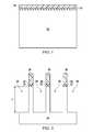
- semiconductor substrate 30is provided.
- semiconductor substrate 30is a bulk silicon substrate.
- Other commonly used materialssuch as carbon, germanium, gallium, arsenic, nitrogen, indium, phosphorus, and the like, may also be included in semiconductor substrate 30 .
- Semiconductor substrate 30may be in the form of a single-crystal material or a compound material.
- Pad layer 32 and mask layer 34are formed on semiconductor substrate 30 .
- Pad layer 32is preferably a thin film formed through a thermal process and thus including silicon oxide. It is used to buffer semiconductor substrate 30 and mask layer 34 so that less stress is generated. Pad layer 32 may also act as an etch stop layer for etching mask layer 34 .
- mask layer 34is formed of silicon nitride using low-pressure chemical vapor deposition (LPCVD). In other embodiments, mask layer 34 is formed by thermal nitridation of silicon, plasma enhanced chemical vapor deposition (PECVD), or plasma anodic nitridation using nitrogen-hydrogen.
- PECVDplasma enhanced chemical vapor deposition
- Mask layer 34may have a thickness of about 60 nm to about 120 nm. It is noted, however, that the dimensions recited throughout the description are merely examples, and may change if the integrated circuits are formed using different technologies.
- photoresist 36is applied on mask layer 34 , and is then patterned, forming openings 38 in photoresist 36 .
- Mask layer 34 and pad layer 32are then etched through openings 38 , exposing underlying semiconductor substrate 30 .
- semiconductor substrate 30is etched, so that openings 38 extend into semiconductor substrate 30 .
- the recessing depth D 1 of semiconductor substrate 30is between about 100 nm and about 300 nm.
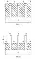
- openings 38are filled with dielectric material 39 , for example, silicon oxide formed by sub-atmospheric chemical vapor deposition (SA-CVD).
- dielectric layer 39is formed by high-density plasma chemical vapor deposition (HDP-CVD) or spin on (with spin-on glass (SOG)).
- a chemical mechanical polish (CMP)is then performed to planarize the surface of the wafer, forming shallow trench isolation (STI) regions 40 , and the resulting structure is shown in FIG. 4 .
- Mask layer 34may be used as a CMP stop layer.
- STI regions 40define substrate portions 41 of silicon substrate 30 (refer to FIG. 3 ).
- Substrate portions 41are also referred to extension portions of substrate 30 (with the portion of substrate 30 underlying STI regions 40 being treated as a substrate).
- width W 1 of substrate portion 41is between about 5 nm and about 30 nm.
- the remaining portions of mask layer 34 and pad layer 32are removed.
- the exposed STI regions 40are recessed and the resulting structure is shown in FIG. 6 .
- top portions 42 of substrate extension portions 41are above the top surface of remaining STI regions 40 to form fins 42 .
- the recessing depth D 2 of the recessesis between about 20 nm and about 90 nm.
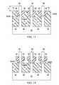
- silicon germanium (SiGe) layer 44is selectively formed on fins 42 , for example, through an epitaxial growth.
- the silicon germanium in SiGe layer 44may be expressed as Si 1-x Ge x , wherein x is the atomic percentage of germanium. In an exemplary embodiment, x is between about 0.15 and about 0.45. Thickness T of SiGe layer 44 may be between about 10 nm and about 30 nm.
- an optional isotropic etchis performed using an etchant attacking STI regions 40 , but not substrate portions 42 / 41 and SiGe layer 44 . Accordingly, SiGe layer 44 acts as a mask.
- the resulting undercuts 50extend under SiGe layer 44 , and the sidewalls of substrate portions 41 are exposed. Height H of undercuts 50 may be between about 2 nm and about 5 nm, although a greater or a smaller height may also apply. In alternative embodiments, the step performed in FIG. 8 may be skipped, and no undercut is formed.
- a condensation stepis performed.
- the condensationmay be preformed at a temperature between about 850° C. and 1100° C. in an oxygen-containing environment (such as an oven), in which oxygen-containing gases, such as O 2 , are introduced.
- oxygen-containing gasessuch as O 2
- the condensationresults in the formation of silicon oxide layer 52 from the outer SiGe film due to the presence of oxygen.
- Germanium atoms in the SiGe filmmigrate inwardly to form SiGe fins 54 .
- the silicon germanium in SiGe fins 54may be expressed as Si 1-y Ge y , wherein y is the atomic percentage of germanium. Germanium percentage y may be between about 20 and about 80 percent.
- germanium percentage ymay be close to 1, which means that SiGe fins 54 are formed of substantially pure germanium. With the condensation step being controlled, the germanium percentage y may be greater than the germanium percentage x in SiGe layer 44 ( FIG. 7 ). This may be achieved, for example, by adjusting the thickness of SiGe layer 44 and the process conditions of the condensation. The germanium percentage y may be increased by increasing the thickness of SiGe layer 44 and increasing germanium percentage x in SiGe layer 44 .
- SiGe fins 54are bottom-notched and include neck regions 54 ′ that are narrower than the upper portions of SiGe fins 54 .
- width W 3 of silicon SiGe neck regions 54 ′may be less than about 50 percent, or even less than about 20 percent of the width W 2 of a top portion of silicon SiGe fins 54 . Further, width W 3 may be less than about 5 nm. Alternatively, no neck region 54 ′ exists (width W 3 is equal to zero). Further, in neck regions 54 ′, the atomic percentage of germanium decrease from top to bottom, and at some point, neck regions 54 ′ merge with substrate portions 41 .
- germanium percentagedecreases, which means that the germanium percentages in outer portions of SiGe fins 54 may be higher than the germanium percentages in inner portions (including the center) of SiGe fins 54 .
- FIG. 9Billustrates an alternative embodiment, wherein close to undercut regions 50 ( FIG. 8 ), the portions of silicon oxide layer 52 on opposite sides of neck regions 54 ′ merge together, so that silicon oxide layer 52 extends directly underlying neck regions 54 ′, and SiGe fins 54 are electrically insulated from the respective underlying substrate portions 41 .
- a uniform SiGe concentration fincan be formed.
- oxide layer 52is removed, for example, by an isotropic etch, and the resulting structure is shown, in which SiGe fins 54 are exposed.
- FinFET 60may be formed based on SiGe fins 54 , as is shown in FIGS. 11A and 11B .
- FIG. 11Billustrates a cross-sectional view taken from a plane crossing line 11 B- 11 B in FIG. 11A .
- the resulting FinFET 60may include lightly doped source and drain regions 62 , source and drain regions 64 , gate spacers 66 , gate dielectric 68 , and gate electrodes 69 .
- Gate dielectric 68may be formed of a high-k dielectric material, for example, with a k value greater than about 7.
- FIGS. 12 through 15illustrate cross-sectional views of intermediate stages in the manufacturing of another embodiment.
- the materials and formation details of the components in this embodimentare essentially the same as the like components, which are denoted by like reference numerals, in the embodiment shown in FIGS. 1 through 11B .
- the formation details of the embodiment shown in FIGS. 12 through 15may thus be found in the discussion of the embodiment shown in FIGS. 1 through 11B .
- the initial steps of this embodimentare essentially the same as shown in FIGS. 1 through 9B .
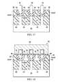
- sacrificial dielectric material 70is filled into the gaps between (as shown in FIG. 9A ) SiGe fins 54 and oxide layer 52 .
- high aspect ratio process (HARP) oxideis used to fill sacrificial dielectric material 70 , although sacrificial dielectric material 70 may also be filled using other methods with a good gap-filling ability, such as spin-on, sub-atmospheric chemical vapor deposition (SA-CVD), and even high-density plasma CVD (HDP-CVD).
- SA-CVDsub-atmospheric chemical vapor deposition
- HDP-CVDhigh-density plasma CVD
- the top surface of sacrificial dielectric material 70is lower than the top surface of oxide layer 52 .
- the filling of dielectric material 70is performed until the top surface of sacrificial dielectric material 70 is higher than the top surface of oxide layer 52 .
- a CMP and/or an etch-backis then performed to lower the surface of sacrificial dielectric material 70 to form the structure as shown in FIG. 12 .
- Sacrificial dielectric material 70may have a high etching selectivity with oxide layer 52 , so that oxide layer 52 remains un-removed.
- the exposed upper portions of oxide layer 52 not protected by sacrificial dielectric material 70are etched, and SiGe fins 54 are exposed.
- the height H′ of SiGe fins 54may be adjusted by adjusting the height of remaining lower portions of oxide layer 52 .
- sacrificial dielectric material 70is removed, for example, using an isotropic etch.
- the lower portions of dielectric layer 52remain to protect the sidewalls of lower portions of SiGe fins 54 , so that SiGe fins 54 are less likely to be broken.
- FinFET 60is formed based on SiGe fin(s) 54 .
- FIGS. 16 through 18illustrate cross-sectional views of intermediate stages in the manufacturing of yet another embodiment.
- dielectric material 80is filled into the gaps between SiGe fins 54 and oxide layer 52 , until the top surface of dielectric material 80 is higher than the top surface of oxide layer 52 .
- spin-onis used to fill dielectric material into the gaps shown in FIG. 9A or 9 B, although other methods having good gap-filling ability may also be used.
- a CMPis then performed to lower the surface of dielectric material 80 .
- Dielectric material 80may be formed of an oxide, such as silicon oxide, although other dielectric materials may also be used.
- a selective etch backis performed to recess oxide layer 52 and dielectric material 80 , resulting in the structure as shown in FIG. 17 .
- the recessing of oxide layer 52 and dielectric material 80may be performed simultaneously.
- the top portions of SiGe fins 54are thus exposed.
- the recessing depthmay be adjusted to adjust the height of SiGe fins 54 , which will be used to form FinFETs.
- FinFET 60is formed on SiGe fin(s) 54 .
- the germanium percentage in SiGe finsmay be freely tuned, and can be much higher than the as-deposited germanium concentration in the deposited SiGe films. Also, the dislocation defects in the condensed SiGe fins may also be reduced as compared to the defects in the SiGe formed by epitaxial growth.
- the neck regions in the SiGe finsmay significantly reduce, and possibly eliminate, the punch-through currents in the resulting FinFETs.
- the channel regions of the FinFETsdo not require high impurity (well) concentrations, and the fin heights may be increased in order to increase the drive currents of the FinFETs without incurring the penalty of increased leakage currents.
Landscapes
- Insulated Gate Type Field-Effect Transistor (AREA)
Abstract
Description
- This disclosure relates generally to semiconductor devices, and particularly to structures and formation methods of fin field-effect transistors (FinFETs) having silicon germanium fins.
- Germanium is a commonly known semiconductor material. The electron mobility and hole mobility of germanium are greater than that of silicon, hence making germanium an excellent material in the formation of integrated circuits. However, in the past, silicon gained more popularity since its oxide (silicon oxide) is readily usable in the gate dielectric of metal-oxide-semiconductor (MOS) transistors. The gate dielectrics of the MOS transistors can be conveniently formed by thermal oxidation of silicon substrates. The oxides of germanium, on the other hand, are either soluble in water or may evaporate at temperatures above 425 C, and hence are not compatible with traditional IC processing.
- With the use of high-k dielectric materials in the gate dielectrics of MOS transistors, the convenience provided by the silicon oxide is no longer a big advantage, and hence germanium is reexamined for use in integrated circuits. Recent studies of using germanium in Fin field-effect transistors (FinFETs) have been reported.
- To reduce the leakage of MOS transistors and to increase the drive currents of germanium FinFETs, germanium-on-insulator (GOI) structures may be used. However, the price of GOI substrates (and strained GOI (SGOI) substrates) is significantly higher than that of silicon substrates and it is not practical for foundries to buy GOI substrates or SGOI substrates. Further, the technology and materials for processing silicon germanium, for example, selecting and controlling the chemicals for processing silicon germanium, are still being explored.
- Conventionally, silicon germanium fins may also be formed by forming shallow trench isolation (STI) regions in the silicon substrate, recessing the portions of the silicon substrate between the STI regions to form recesses, epitaxially growing silicon germanium in the recesses, and then recessing the STI regions so that the epitaxially grown silicon germanium becomes silicon germanium fins. This approach, however, involves performing the chemical mechanical polish (CMP) on the silicon germanium, and hence also involves high manufacturing costs and the use of immature technology.
- In accordance with one aspect of the embodiment, an integrated circuit structure includes a substrate and a germanium-containing semiconductor fin over the substrate. The germanium-containing semiconductor fin has an upper portion having a first width, and a neck region under the upper portion and having a second width smaller than the first width.
- Other embodiments are also disclosed.
- For a more complete understanding of the embodiments, and the advantages thereof, reference is now made to the following descriptions taken in conjunction with the accompanying drawings, in which:
FIGS. 1 through 11B are cross-sectional views of intermediate stages in the manufacturing of a fin field-effect transistor (FinFET) in accordance with an embodiment; andFIGS. 12 through 18 are cross-sectional views of intermediate stages in the manufacturing of a FinFET in accordance with alternative embodiments.- The making and using of the embodiments of the disclosure are discussed in detail below. It should be appreciated, however, that the embodiments provide many applicable inventive concepts that can be embodied in a wide variety of specific contexts. The specific embodiments discussed are merely illustrative and do not limit the scope of the disclosure.
- A novel fin field-effect transistor (FinFET) and the method for forming the same are provided. The variations of the embodiment are discussed. Throughout the various views and illustrative embodiments, like reference numbers are used to designate like elements.
- Referring to
FIG. 1 ,semiconductor substrate 30 is provided. In an embodiment,semiconductor substrate 30 is a bulk silicon substrate. Other commonly used materials, such as carbon, germanium, gallium, arsenic, nitrogen, indium, phosphorus, and the like, may also be included insemiconductor substrate 30.Semiconductor substrate 30 may be in the form of a single-crystal material or a compound material. Pad layer 32 andmask layer 34 are formed onsemiconductor substrate 30.Pad layer 32 is preferably a thin film formed through a thermal process and thus including silicon oxide. It is used to buffersemiconductor substrate 30 andmask layer 34 so that less stress is generated.Pad layer 32 may also act as an etch stop layer foretching mask layer 34. In an embodiment,mask layer 34 is formed of silicon nitride using low-pressure chemical vapor deposition (LPCVD). In other embodiments,mask layer 34 is formed by thermal nitridation of silicon, plasma enhanced chemical vapor deposition (PECVD), or plasma anodic nitridation using nitrogen-hydrogen.Mask layer 34 may have a thickness of about 60 nm to about 120 nm. It is noted, however, that the dimensions recited throughout the description are merely examples, and may change if the integrated circuits are formed using different technologies.- Referring to
FIG. 2 ,photoresist 36 is applied onmask layer 34, and is then patterned, formingopenings 38 inphotoresist 36.Mask layer 34 andpad layer 32 are then etched throughopenings 38, exposingunderlying semiconductor substrate 30. Next,semiconductor substrate 30 is etched, so thatopenings 38 extend intosemiconductor substrate 30. In an exemplary embodiment, the recessing depth D1 ofsemiconductor substrate 30 is between about 100 nm and about 300 nm. - In an embodiment, as shown in
FIG. 3 ,openings 38 are filled withdielectric material 39, for example, silicon oxide formed by sub-atmospheric chemical vapor deposition (SA-CVD). In other embodiments,dielectric layer 39 is formed by high-density plasma chemical vapor deposition (HDP-CVD) or spin on (with spin-on glass (SOG)). A chemical mechanical polish (CMP) is then performed to planarize the surface of the wafer, forming shallow trench isolation (STI)regions 40, and the resulting structure is shown inFIG. 4 .Mask layer 34 may be used as a CMP stop layer. STIregions 40 definesubstrate portions 41 of silicon substrate30 (refer toFIG. 3 ).Substrate portions 41 are also referred to extension portions of substrate30 (with the portion ofsubstrate 30underlying STI regions 40 being treated as a substrate). In an exemplary embodiment, width W1 ofsubstrate portion 41 is between about 5 nm and about 30 nm. - Referring to
FIG. 5 , the remaining portions ofmask layer 34 andpad layer 32 are removed. Next, the exposedSTI regions 40 are recessed and the resulting structure is shown inFIG. 6 . As a result,top portions 42 ofsubstrate extension portions 41 are above the top surface ofremaining STI regions 40 to formfins 42. In an exemplary embodiment, the recessing depth D2 of the recesses is between about 20 nm and about 90 nm. - Referring to
FIG. 7 , silicon germanium (SiGe)layer 44 is selectively formed onfins 42, for example, through an epitaxial growth. The silicon germanium inSiGe layer 44 may be expressed as Si1-xGex, wherein x is the atomic percentage of germanium. In an exemplary embodiment, x is between about 0.15 and about 0.45. Thickness T ofSiGe layer 44 may be between about 10 nm and about 30 nm. - In an embodiment, referring to
FIG. 8 , an optional isotropic etch is performed using an etchant attackingSTI regions 40, but notsubstrate portions 42/41 andSiGe layer 44. Accordingly, SiGelayer 44 acts as a mask. The resultingundercuts 50 extend underSiGe layer 44, and the sidewalls ofsubstrate portions 41 are exposed. Height H ofundercuts 50 may be between about 2 nm and about 5 nm, although a greater or a smaller height may also apply. In alternative embodiments, the step performed inFIG. 8 may be skipped, and no undercut is formed. - Referring to
FIGS. 9A and 9B , a condensation step is performed. The condensation may be preformed at a temperature between about 850° C. and 1100° C. in an oxygen-containing environment (such as an oven), in which oxygen-containing gases, such as O2, are introduced. The condensation results in the formation ofsilicon oxide layer 52 from the outer SiGe film due to the presence of oxygen. Germanium atoms in the SiGe film migrate inwardly to formSiGe fins 54. The silicon germanium inSiGe fins 54 may be expressed as Si1-yGey, wherein y is the atomic percentage of germanium. Germanium percentage y may be between about 20 and about 80 percent. In an exemplary embodiment, germanium percentage y may be close to 1, which means thatSiGe fins 54 are formed of substantially pure germanium. With the condensation step being controlled, the germanium percentage y may be greater than the germanium percentage x in SiGe layer44 (FIG. 7 ). This may be achieved, for example, by adjusting the thickness ofSiGe layer 44 and the process conditions of the condensation. The germanium percentage y may be increased by increasing the thickness ofSiGe layer 44 and increasing germanium percentage x inSiGe layer 44. - Due to the existence of undercuts50 (refer to
FIG. 8 ),SiGe fins 54 are bottom-notched and includeneck regions 54′ that are narrower than the upper portions ofSiGe fins 54. In an embodiment, width W3 of siliconSiGe neck regions 54′ may be less than about 50 percent, or even less than about 20 percent of the width W2 of a top portion ofsilicon SiGe fins 54. Further, width W3 may be less than about 5 nm. Alternatively, noneck region 54′ exists (width W3 is equal to zero). Further, inneck regions 54′, the atomic percentage of germanium decrease from top to bottom, and at some point,neck regions 54′ merge withsubstrate portions 41. Further, as an effect of the migration of germanium atoms from outside to inside, in the upper portions ofSiGe fins 54, for example, in the directions ofarrows 56, the germanium percentage decreases, which means that the germanium percentages in outer portions ofSiGe fins 54 may be higher than the germanium percentages in inner portions (including the center) ofSiGe fins 54. FIG. 9B illustrates an alternative embodiment, wherein close to undercut regions50 (FIG. 8 ), the portions ofsilicon oxide layer 52 on opposite sides ofneck regions 54′ merge together, so thatsilicon oxide layer 52 extends directly underlyingneck regions 54′, andSiGe fins 54 are electrically insulated from the respectiveunderlying substrate portions 41. With this embodiment, a uniform SiGe concentration fin can be formed. By completely shutting off the Ge downward diffusion path (with width W3 being 0) followed by a high temperature anneal, Ge atoms can be uniformly distributed inside the SiGe fin.- In
FIG. 10 ,oxide layer 52 is removed, for example, by an isotropic etch, and the resulting structure is shown, in whichSiGe fins 54 are exposed. Next,FinFET 60 may be formed based onSiGe fins 54, as is shown inFIGS. 11A and 11B .FIG. 11B illustrates a cross-sectional view taken from aplane crossing line 11B-11B inFIG. 11A . The resultingFinFET 60 may include lightly doped source and drainregions 62, source and drainregions 64,gate spacers 66,gate dielectric 68, andgate electrodes 69.Gate dielectric 68 may be formed of a high-k dielectric material, for example, with a k value greater than about 7. The processes for formingcomponents FIGS. 12 through 15 illustrate cross-sectional views of intermediate stages in the manufacturing of another embodiment. Unless specified otherwise, the materials and formation details of the components in this embodiment are essentially the same as the like components, which are denoted by like reference numerals, in the embodiment shown inFIGS. 1 through 11B . The formation details of the embodiment shown inFIGS. 12 through 15 may thus be found in the discussion of the embodiment shown inFIGS. 1 through 11B . The initial steps of this embodiment are essentially the same as shown inFIGS. 1 through 9B .- Next, referring to
FIG. 12 , sacrificialdielectric material 70 is filled into the gaps between (as shown inFIG. 9A )SiGe fins 54 andoxide layer 52. In an embodiment, high aspect ratio process (HARP) oxide is used to fill sacrificialdielectric material 70, although sacrificialdielectric material 70 may also be filled using other methods with a good gap-filling ability, such as spin-on, sub-atmospheric chemical vapor deposition (SA-CVD), and even high-density plasma CVD (HDP-CVD). In an embodiment, as shown inFIG. 12 , the top surface of sacrificialdielectric material 70 is lower than the top surface ofoxide layer 52. In alternative embodiments, the filling ofdielectric material 70 is performed until the top surface of sacrificialdielectric material 70 is higher than the top surface ofoxide layer 52. A CMP and/or an etch-back is then performed to lower the surface of sacrificialdielectric material 70 to form the structure as shown inFIG. 12 . Sacrificialdielectric material 70 may have a high etching selectivity withoxide layer 52, so thatoxide layer 52 remains un-removed. - Referring to
FIG. 13 , the exposed upper portions ofoxide layer 52 not protected by sacrificialdielectric material 70 are etched, andSiGe fins 54 are exposed. The height H′ ofSiGe fins 54 may be adjusted by adjusting the height of remaining lower portions ofoxide layer 52. InFIG. 14 , sacrificialdielectric material 70 is removed, for example, using an isotropic etch. In this embodiment, the lower portions ofdielectric layer 52 remain to protect the sidewalls of lower portions ofSiGe fins 54, so thatSiGe fins 54 are less likely to be broken. Next, as shown in the cross-sectional view ofFIG. 15 ,FinFET 60 is formed based on SiGe fin(s)54. FIGS. 16 through 18 illustrate cross-sectional views of intermediate stages in the manufacturing of yet another embodiment. Again, unless specified otherwise, the materials and formation details of the components in this embodiment are essentially the same as the like components, which are denoted by like reference numerals in the embodiment shown inFIGS. 1 through 11B . Next, referring toFIG. 16 ,dielectric material 80 is filled into the gaps betweenSiGe fins 54 andoxide layer 52, until the top surface ofdielectric material 80 is higher than the top surface ofoxide layer 52. In an embodiment, spin-on is used to fill dielectric material into the gaps shown inFIG. 9A or9B, although other methods having good gap-filling ability may also be used. A CMP is then performed to lower the surface ofdielectric material 80.Dielectric material 80 may be formed of an oxide, such as silicon oxide, although other dielectric materials may also be used.- Referring to
FIG. 17 , a selective etch back is performed to recessoxide layer 52 anddielectric material 80, resulting in the structure as shown inFIG. 17 . The recessing ofoxide layer 52 anddielectric material 80 may be performed simultaneously. The top portions ofSiGe fins 54 are thus exposed. The recessing depth may be adjusted to adjust the height ofSiGe fins 54, which will be used to form FinFETs. Next, as shown in the cross-sectional view ofFIG. 18 ,FinFET 60 is formed on SiGe fin(s)54. - In the embodiments, with the condensation approach, the germanium percentage in SiGe fins may be freely tuned, and can be much higher than the as-deposited germanium concentration in the deposited SiGe films. Also, the dislocation defects in the condensed SiGe fins may also be reduced as compared to the defects in the SiGe formed by epitaxial growth.
- The neck regions in the SiGe fins may significantly reduce, and possibly eliminate, the punch-through currents in the resulting FinFETs. As a result, the channel regions of the FinFETs do not require high impurity (well) concentrations, and the fin heights may be increased in order to increase the drive currents of the FinFETs without incurring the penalty of increased leakage currents.
- Although the embodiments and their advantages have been described in detail, it should be understood that various changes, substitutions, and alterations can be made herein without departing from the spirit and scope of the embodiments as defined by the appended claims. Moreover, the scope of the present application is not intended to be limited to the particular embodiments of the process, machine, manufacture, and composition of matter, means, methods and steps described in the specification. As one of ordinary skill in the art will readily appreciate from the disclosure, processes, machines, manufacture, compositions of matter, means, methods, or steps, presently existing or later to be developed, that perform substantially the same function or achieve substantially the same result as the corresponding embodiments described herein may be utilized according to the disclosure. Accordingly, the appended claims are intended to include within their scope such processes, machines, manufacture, compositions of matter, means, methods, or steps. In addition, each claim constitutes a separate embodiment, and the combination of various claims and embodiments are within the scope of the disclosure.
Claims (18)
1. An integrated circuit structure comprising:
a substrate; and
a germanium-containing semiconductor fin over the substrate, wherein the germanium-containing semiconductor fin comprises an upper portion having a first width, and a neck region under the upper portion and having a second width smaller than the first width.
2. The integrated circuit structure ofclaim 1 further comprising:
two insulation regions on opposite sides of the germanium-containing semiconductor fin; and
an extension portion of the substrate between and adjoining the two insulation regions, wherein the extension portion is directly underlying the germanium-containing semiconductor fin.
3. The integrated circuit structure ofclaim 2 , wherein top surfaces of the two insulation regions are lower than a bottom end of the neck region.
4. The integrated circuit structure ofclaim 2 , wherein a bottom end of the neck region adjoins the extension portion of the substrate.
5. The integrated circuit structure ofclaim 2 further comprising a silicon oxide region electrically insulating a bottom end of the neck region from the extension portion of the substrate.
6. The integrated circuit structure ofclaim 1 further comprising:
a gate dielectric of a FinFET on a top surface and sidewalls of the germanium-containing semiconductor fin; and
a gate electrode of the FinFET on the gate dielectric.
7. The integrated circuit structure ofclaim 1 , wherein the substrate is a silicon substrate, and wherein the germanium-containing semiconductor fin comprises silicon germanium.
8. The integrated circuit structure ofclaim 1 , wherein the germanium-containing semiconductor fin has a germanium atomic percentage higher than about 15 percent.
9. The integrated circuit structure ofclaim 1 , wherein the second width is less than about 5 nm.
10. An integrated circuit structure comprising:
a silicon substrate;
a silicon germanium (SiGe) fin over the silicon substrate, wherein the SiGe fin comprises an upper portion having a first width, and a lower portion comprising a neck region having a second width smaller than the first width;
two insulation regions on opposite sides of the SiGe fin;
an extension portion of the silicon substrate between and adjoining the two insulation regions, wherein the extension portion is directly underlying the SiGe fin;
a silicon oxide layer on sidewalls of the lower portion of the SiGe fin and not on sidewalls of the upper portion of the SiGe fin;
a gate dielectric of a FinFET on a top surface and sidewalls of the SiGe fin, wherein the gate dielectric comprises a bottom end contacting a top end of the silicon oxide layer; and
a gate electrode of the FinFET on the gate dielectric.
11. The integrated circuit structure ofclaim 10 , wherein top surfaces of the insulation regions are lower than a bottom end of the neck region.
12. The integrated circuit structure ofclaim 10 , wherein the SiGe fin has a germanium atomic percentage between about 20 percent and about 80 percent.
13. The integrated circuit structure ofclaim 10 , wherein the second width is less than about 5 nm.
14. The integrated circuit structure ofclaim 10 , wherein a bottom end of the neck region adjoins the extension portion of the silicon substrate.
15. The integrated circuit structure ofclaim 10 further comprising a silicon oxide region separating a bottom end of the neck region from the extension portion of the silicon substrate.
16. An integrated circuit structure comprising:
a silicon substrate; and
a silicon germanium (SiGe) fin over the silicon substrate; and
an oxide region between, and adjoining, a portion of the silicon substrate.
17. The integrated circuit structure ofclaim 16 further comprising two insulation regions in the silicon substrate, with the portion of the silicon substrate between and adjoining the two insulation regions, and wherein the oxide region is over the two insulation regions.
18. The integrated circuit structure ofclaim 16 wherein the oxide region further extends to sidewalls of the SiGe fin.
Priority Applications (2)
| Application Number | Priority Date | Filing Date | Title |
|---|---|---|---|
| US12/702,862US8395195B2 (en) | 2010-02-09 | 2010-02-09 | Bottom-notched SiGe FinFET formation using condensation |
| US13/794,458US8703565B2 (en) | 2010-02-09 | 2013-03-11 | Bottom-notched SiGe FinFET formation using condensation |
Applications Claiming Priority (1)
| Application Number | Priority Date | Filing Date | Title |
|---|---|---|---|
| US12/702,862US8395195B2 (en) | 2010-02-09 | 2010-02-09 | Bottom-notched SiGe FinFET formation using condensation |
Related Child Applications (1)
| Application Number | Title | Priority Date | Filing Date |
|---|---|---|---|
| US13/794,458ContinuationUS8703565B2 (en) | 2010-02-09 | 2013-03-11 | Bottom-notched SiGe FinFET formation using condensation |
Publications (2)
| Publication Number | Publication Date |
|---|---|
| US20110193178A1true US20110193178A1 (en) | 2011-08-11 |
| US8395195B2 US8395195B2 (en) | 2013-03-12 |
Family
ID=44353019
Family Applications (2)
| Application Number | Title | Priority Date | Filing Date |
|---|---|---|---|
| US12/702,862Active2030-11-11US8395195B2 (en) | 2010-02-09 | 2010-02-09 | Bottom-notched SiGe FinFET formation using condensation |
| US13/794,458Expired - Fee RelatedUS8703565B2 (en) | 2010-02-09 | 2013-03-11 | Bottom-notched SiGe FinFET formation using condensation |
Family Applications After (1)
| Application Number | Title | Priority Date | Filing Date |
|---|---|---|---|
| US13/794,458Expired - Fee RelatedUS8703565B2 (en) | 2010-02-09 | 2013-03-11 | Bottom-notched SiGe FinFET formation using condensation |
Country Status (1)
| Country | Link |
|---|---|
| US (2) | US8395195B2 (en) |
Cited By (83)
| Publication number | Priority date | Publication date | Assignee | Title |
|---|---|---|---|---|
| US20130015591A1 (en)* | 2011-07-12 | 2013-01-17 | Invensas Corporation | Memory module in a package |
| CN103000524A (en)* | 2011-09-13 | 2013-03-27 | 中芯国际集成电路制造(上海)有限公司 | Fin field-effect transistor and manufacturing method thereof |
| US20130109152A1 (en)* | 2010-02-09 | 2013-05-02 | Taiwan Semiconductor Manufacturing Co., Ltd. | Method of making lower parasitic capacitance finfet |
| US20130168748A1 (en)* | 2011-12-29 | 2013-07-04 | Wayne BAO | Fin fet structure with dual-stress spacers and method for forming the same |
| US8513073B1 (en) | 2012-08-27 | 2013-08-20 | International Business Machines Corporation | Silicon germanium channel with silicon buffer regions for fin field effect transistor device |
| US8525327B2 (en) | 2011-10-03 | 2013-09-03 | Invensas Corporation | Stub minimization for assemblies without wirebonds to package substrate |
| CN103378156A (en)* | 2012-04-26 | 2013-10-30 | 台湾积体电路制造股份有限公司 | Multi-gate devices with replaced-channels and methods for forming the same |
| US8653646B2 (en) | 2011-10-03 | 2014-02-18 | Invensas Corporation | Stub minimization using duplicate sets of terminals for wirebond assemblies without windows |
| US8659142B2 (en) | 2011-10-03 | 2014-02-25 | Invensas Corporation | Stub minimization for wirebond assemblies without windows |
| US8659139B2 (en) | 2011-10-03 | 2014-02-25 | Invensas Corporation | Stub minimization using duplicate sets of signal terminals in assemblies without wirebonds to package substrate |
| US8669147B2 (en)* | 2012-06-11 | 2014-03-11 | Globalfoundries Inc. | Methods of forming high mobility fin channels on three dimensional semiconductor devices |
| US8670261B2 (en) | 2011-10-03 | 2014-03-11 | Invensas Corporation | Stub minimization using duplicate sets of signal terminals |
| US20140084351A1 (en)* | 2012-09-27 | 2014-03-27 | Taiwan Semiconductor Manufacturing Co., Ltd. | Replacement channels for semiconductor devices and methods for forming the same using dopant concentration boost |
| US20140099774A1 (en)* | 2012-10-05 | 2014-04-10 | Imec | Method for Producing Strained Ge Fin Structures |
| EP2709156A3 (en)* | 2012-09-14 | 2014-04-23 | Imec | Band engineered semiconductor device and method for manufacturing thereof |
| WO2014071653A1 (en)* | 2012-11-09 | 2014-05-15 | 中国科学院微电子研究所 | Semiconductor device and manufacturing method therefor |
| CN103811325A (en)* | 2012-11-13 | 2014-05-21 | 中芯国际集成电路制造(上海)有限公司 | Fin type field effect transistor forming method |
| EP2738814A1 (en)* | 2012-11-30 | 2014-06-04 | STMicroelectronics Inc | Finfet device with isolated channel |
| US8759982B2 (en) | 2011-07-12 | 2014-06-24 | Tessera, Inc. | Deskewed multi-die packages |
| US20140197457A1 (en)* | 2013-01-14 | 2014-07-17 | Taiwan Semiconductor Manufacturing Company Ltd. | FinFET Device and Method of Fabricating Same |
| US8787034B2 (en) | 2012-08-27 | 2014-07-22 | Invensas Corporation | Co-support system and microelectronic assembly |
| US8823165B2 (en) | 2011-07-12 | 2014-09-02 | Invensas Corporation | Memory module in a package |
| CN104051502A (en)* | 2013-03-14 | 2014-09-17 | 国际商业机器公司 | Formation of Bulk SiGe Fins with Dielectric Isolation by Anodization |
| US8848392B2 (en) | 2012-08-27 | 2014-09-30 | Invensas Corporation | Co-support module and microelectronic assembly |
| US8848391B2 (en) | 2012-08-27 | 2014-09-30 | Invensas Corporation | Co-support component and microelectronic assembly |
| CN104103520A (en)* | 2013-04-11 | 2014-10-15 | 国际商业机器公司 | Method for forming FinFET device and FinFET structure |
| US8917532B2 (en) | 2011-10-03 | 2014-12-23 | Invensas Corporation | Stub minimization with terminal grids offset from center of package |
| US20140374838A1 (en)* | 2013-06-21 | 2014-12-25 | Taiwan Semiconductor Manufacturing Company, Ltd. | FinFETs with Nitride Liners and Methods of Forming the Same |
| US8956942B2 (en) | 2012-12-21 | 2015-02-17 | Stmicroelectronics, Inc. | Method of forming a fully substrate-isolated FinFET transistor |
| WO2015026428A1 (en)* | 2013-08-21 | 2015-02-26 | Tel Epion Inc. | Gcib etching method for adjusting fin height of finfet devices |
| US8981547B2 (en) | 2011-10-03 | 2015-03-17 | Invensas Corporation | Stub minimization for multi-die wirebond assemblies with parallel windows |
| US20150115216A1 (en)* | 2012-12-20 | 2015-04-30 | Intel Corporation | Conversion of thin transistor elements from silicon to silicon germanium |
| US20150132901A1 (en)* | 2013-01-14 | 2015-05-14 | Taiwan Semiconductor Manufacturing Company, Ltd. | Semiconductor Device and Fabricating the Same |
| US9070423B2 (en) | 2013-06-11 | 2015-06-30 | Invensas Corporation | Single package dual channel memory with co-support |
| US20150187909A1 (en)* | 2013-12-30 | 2015-07-02 | Global Foundries, Inc. | Methods for fabricating multiple-gate integrated circuits |
| WO2015102884A1 (en)* | 2014-01-03 | 2015-07-09 | Qualcomm Incorporated | Silicon germanium finfet formation by ge condensation |
| US20150214226A1 (en)* | 2014-01-24 | 2015-07-30 | Taiwan Semiconductor Manufacturing Company, Ltd. | Method and structure for gap filling improvement |
| US9099423B2 (en) | 2013-07-12 | 2015-08-04 | Asm Ip Holding B.V. | Doped semiconductor films and processing |
| US20150221726A1 (en)* | 2014-02-04 | 2015-08-06 | Globalfoundries Inc. | Finfet with isolated source and drain |
| US9123555B2 (en) | 2013-10-25 | 2015-09-01 | Invensas Corporation | Co-support for XFD packaging |
| US9153692B2 (en) | 2013-04-09 | 2015-10-06 | Samsung Electronics Co., Ltd. | Semiconductor device having a stress film on a side surface of a fin |
| US20150303305A1 (en)* | 2014-04-16 | 2015-10-22 | Taiwan Semiconductor Manufacturing Company, Ltd. | FinFET Device with High-K Metal Gate Stack |
| KR20150119814A (en)* | 2014-04-16 | 2015-10-26 | 타이완 세미콘덕터 매뉴팩쳐링 컴퍼니 리미티드 | A method and structure for finfet device |
| US20150311320A1 (en)* | 2014-04-25 | 2015-10-29 | International Business Machines Corporation | Fin formation in fin field effect transistors |
| CN105280558A (en)* | 2014-06-27 | 2016-01-27 | 台湾积体电路制造股份有限公司 | Structure and method for FinFET device |
| US9281296B2 (en) | 2014-07-31 | 2016-03-08 | Invensas Corporation | Die stacking techniques in BGA memory package for small footprint CPU and memory motherboard design |
| US9281378B2 (en) | 2012-01-24 | 2016-03-08 | Taiwan Semiconductor Manufacturing Company, Ltd. | Fin recess last process for FinFET fabrication |
| US20160079427A1 (en)* | 2014-06-27 | 2016-03-17 | Taiwan Semiconductor Manufacturing Company, Ltd. | Structure and method for sram finfet device |
| US9299809B2 (en)* | 2012-12-17 | 2016-03-29 | Globalfoundries Inc. | Methods of forming fins for a FinFET device wherein the fins have a high germanium content |
| US9343300B1 (en) | 2015-04-15 | 2016-05-17 | Globalfoundries Inc. | Methods of forming source/drain regions for a PMOS transistor device with a germanium-containing channel region |
| US9349837B2 (en) | 2012-11-09 | 2016-05-24 | Taiwan Semiconductor Manufacturing Company, Ltd. | Recessing STI to increase Fin height in Fin-first process |
| US9368477B2 (en) | 2012-08-27 | 2016-06-14 | Invensas Corporation | Co-support circuit panel and microelectronic packages |
| US20160197147A1 (en)* | 2014-09-05 | 2016-07-07 | International Business Machines Corporation | High germanium content silicon germanium fins |
| US9406749B2 (en)* | 2014-10-02 | 2016-08-02 | Taiwan Semiconductor Manufacturing Company Limited | Method of manufacturing a horizontal gate-all-around transistor having a fin |
| US9443962B2 (en) | 2012-11-09 | 2016-09-13 | Taiwan Semiconductor Manufacturing Company, Ltd. | Recessing STI to increase fin height in fin-first process |
| US9466696B2 (en) | 2012-01-24 | 2016-10-11 | Taiwan Semiconductor Manufacturing Company, Ltd. | FinFETs and methods for forming the same |
| US9472573B2 (en)* | 2014-12-30 | 2016-10-18 | International Business Machines Corporation | Silicon-germanium fin formation |
| US20160307899A1 (en)* | 2013-09-16 | 2016-10-20 | Stmicroelectronics, Inc. | Method to induce strain in finfet channels from an adjacent region |
| US9484080B1 (en) | 2015-11-09 | 2016-11-01 | Invensas Corporation | High-bandwidth memory application with controlled impedance loading |
| US9525068B1 (en)* | 2013-03-15 | 2016-12-20 | Altera Corporation | Variable gate width FinFET |
| US9679613B1 (en) | 2016-05-06 | 2017-06-13 | Invensas Corporation | TFD I/O partition for high-speed, high-density applications |
| US9691437B2 (en) | 2014-09-25 | 2017-06-27 | Invensas Corporation | Compact microelectronic assembly having reduced spacing between controller and memory packages |
| US9698058B2 (en) | 2014-04-25 | 2017-07-04 | Taiwan Semiconductor Manufacturing Company, Ltd. | Structure and method for FinFET device |
| US9721955B2 (en) | 2014-04-25 | 2017-08-01 | Taiwan Semiconductor Manufacturing Company, Ltd. | Structure and method for SRAM FinFET device having an oxide feature |
| US9761667B2 (en)* | 2015-07-30 | 2017-09-12 | International Business Machines Corporation | Semiconductor structure with a silicon germanium alloy fin and silicon germanium alloy pad structure |
| US20170309623A1 (en)* | 2016-04-21 | 2017-10-26 | Globalfoundries Inc. | Method, apparatus, and system for increasing drive current of finfet device |
| US9831342B2 (en) | 2013-07-29 | 2017-11-28 | Stmicroelectronics | Method to induce strain in 3-D microfabricated structures |
| GB2522826B (en)* | 2012-12-20 | 2017-12-06 | Intel Corp | Epitaxial film on nanoscale structure |
| US9935011B2 (en) | 2013-01-14 | 2018-04-03 | Taiwan Semiconductor Manufacturing Company, Ltd. | Fin spacer protected source and drain regions in FinFETs |
| EP3382761A1 (en)* | 2017-03-29 | 2018-10-03 | IMEC vzw | Integration of silicon-germanium semiconductor structures |
| US10446669B2 (en)* | 2017-11-30 | 2019-10-15 | Taiwan Semiconductor Manufacturing Co., Ltd. | Source and drain surface treatment for multi-gate field effect transistors |
| US20200083358A1 (en)* | 2013-03-08 | 2020-03-12 | Taiwan Semiconductor Manufacturing Company, Ltd. | FinFETs and Methods for Forming the Same |
| US10622480B2 (en)* | 2013-01-14 | 2020-04-14 | Taiwan Semiconductor Manufacturing Company, Ltd. | Forming gate stacks of FinFETs through oxidation |
| US10727301B2 (en)* | 2013-12-30 | 2020-07-28 | Taiwan Semiconductor Manufacturing Company, Ltd. | Semiconductor liner of semiconductor device |
| CN112086503A (en)* | 2019-06-13 | 2020-12-15 | 中芯国际集成电路制造(上海)有限公司 | Semiconductor structure and method of forming the same |
| CN112635560A (en)* | 2019-10-08 | 2021-04-09 | 联华电子股份有限公司 | Fin-shaped transistor structure and manufacturing method thereof |
| CN112670179A (en)* | 2019-10-15 | 2021-04-16 | 中芯国际集成电路制造(上海)有限公司 | Semiconductor structure and forming method thereof |
| CN112786452A (en)* | 2019-11-08 | 2021-05-11 | 中芯国际集成电路制造(上海)有限公司 | Semiconductor structure and forming method thereof |
| CN112864247A (en)* | 2019-11-26 | 2021-05-28 | 中芯国际集成电路制造(上海)有限公司 | Semiconductor structure and forming method thereof |
| US11024708B1 (en)* | 2019-11-14 | 2021-06-01 | Institute of Microelectronics, Chinese Academy of Sciences | Semiconductor device and method for manufacturing the same |
| US20210366715A1 (en)* | 2018-10-31 | 2021-11-25 | Taiwan Semiconductor Manufacturing Co., Ltd. | Semiconductor Device and Method |
| TWI841037B (en)* | 2022-11-04 | 2024-05-01 | 南亞科技股份有限公司 | Semiconductor device and manufacturing method thereof |
| US12243871B2 (en)* | 2018-09-18 | 2025-03-04 | Taiwan Semiconductor Manufacturing Co., Ltd. | Integrated circuits with capacitors |
Families Citing this family (120)
| Publication number | Priority date | Publication date | Assignee | Title |
|---|---|---|---|---|
| US8367498B2 (en) | 2010-10-18 | 2013-02-05 | Taiwan Semiconductor Manufacturing Company, Ltd. | Fin-like field effect transistor (FinFET) device and method of manufacturing same |
| JP5646416B2 (en)* | 2011-09-01 | 2014-12-24 | 株式会社東芝 | Manufacturing method of semiconductor device |
| US8987835B2 (en)* | 2012-03-27 | 2015-03-24 | Taiwan Semiconductor Manufacturing Company, Ltd. | FinFET with a buried semiconductor material between two fins |
| US9287178B2 (en) | 2012-10-01 | 2016-03-15 | Globalfoundries Inc. | Multi-gate field effect transistor (FET) including isolated fin body |
| US8946014B2 (en)* | 2012-12-28 | 2015-02-03 | Taiwan Semiconductor Manufacturing Company, Ltd. | FinFET device structure and methods of making same |
| US8753940B1 (en)* | 2013-03-15 | 2014-06-17 | Globalfoundries Inc. | Methods of forming isolation structures and fins on a FinFET semiconductor device |
| US8969155B2 (en)* | 2013-05-10 | 2015-03-03 | International Business Machines Corporation | Fin structure with varying isolation thickness |
| US8975168B2 (en)* | 2013-05-28 | 2015-03-10 | Stmicroelectronics, Inc. | Method for the formation of fin structures for FinFET devices |
| US9252016B2 (en)* | 2013-09-04 | 2016-02-02 | Globalfoundries Inc. | Stacked nanowire |
| US9553012B2 (en) | 2013-09-13 | 2017-01-24 | Taiwan Semiconductor Manufacturing Company Ltd. | Semiconductor structure and the manufacturing method thereof |
| US9418902B2 (en)* | 2013-10-10 | 2016-08-16 | Globalfoundries Inc. | Forming isolated fins from a substrate |
| US9716176B2 (en) | 2013-11-26 | 2017-07-25 | Samsung Electronics Co., Ltd. | FinFET semiconductor devices including recessed source-drain regions on a bottom semiconductor layer and methods of fabricating the same |
| CN104752214B (en)* | 2013-12-30 | 2018-06-01 | 中芯国际集成电路制造(上海)有限公司 | The forming method of fin field effect pipe |
| US9548303B2 (en) | 2014-03-13 | 2017-01-17 | Taiwan Semiconductor Manufacturing Company, Ltd. | FinFET devices with unique fin shape and the fabrication thereof |
| US9985030B2 (en)* | 2014-04-07 | 2018-05-29 | International Business Machines Corporation | FinFET semiconductor device having integrated SiGe fin |
| US9524986B2 (en) | 2014-06-26 | 2016-12-20 | Globalfoundries Inc. | Trapping dislocations in high-mobility fins below isolation layer |
| KR102219678B1 (en) | 2014-08-12 | 2021-02-25 | 삼성전자주식회사 | Semiconductor device and method for manufacturing the same |
| US9391201B2 (en) | 2014-11-25 | 2016-07-12 | Taiwan Semiconductor Manufacturing Company, Ltd. | Source/drain structure and manufacturing the same |
| US9349652B1 (en) | 2014-12-12 | 2016-05-24 | Taiwan Semiconductor Manufacturing Company, Ltd. | Method of forming semiconductor device with different threshold voltages |
| US9455141B2 (en) | 2014-12-18 | 2016-09-27 | GlobalFoundries, Inc. | Silicon-germanium fin of height above critical thickness |
| US9780214B2 (en) | 2014-12-22 | 2017-10-03 | Taiwan Semiconductor Manufacturing Co., Ltd. | Semiconductor device including Fin- FET and manufacturing method thereof |
| US10141310B2 (en) | 2014-12-23 | 2018-11-27 | Taiwan Semiconductor Manufacturing Company, Ltd. | Short channel effect suppression |
| US10134871B2 (en) | 2014-12-23 | 2018-11-20 | Taiwan Semiconductor Manufacturing Company, Ltd. | Doping of high-K dielectric oxide by wet chemical treatment |
| US9768301B2 (en) | 2014-12-23 | 2017-09-19 | Taiwan Semiconductor Manufacturing Company, Ltd. | Short channel effect suppression |
| US9515071B2 (en) | 2014-12-24 | 2016-12-06 | Taiwan Semiconductor Manufacturing Company, Ltd. | Asymmetric source/drain depths |
| US9425250B2 (en) | 2014-12-30 | 2016-08-23 | Taiwan Semiconductor Manufacturing Company, Ltd. | Transistor with wurtzite channel |
| US9647090B2 (en) | 2014-12-30 | 2017-05-09 | Taiwan Semiconductor Manufacturing Company, Ltd. | Surface passivation for germanium-based semiconductor structure |
| US9614057B2 (en) | 2014-12-30 | 2017-04-04 | International Business Machines Corporation | Enriched, high mobility strained fin having bottom dielectric isolation |
| US9601626B2 (en) | 2015-01-23 | 2017-03-21 | Taiwan Semiconductor Manufacturing Co., Ltd. | Semiconductor device including fin structure with two channel layers and manufacturing method thereof |
| US9484201B2 (en) | 2015-02-23 | 2016-11-01 | International Business Machines Corporation | Epitaxial silicon germanium fin formation using sacrificial silicon fin templates |
| US9406529B1 (en) | 2015-03-05 | 2016-08-02 | International Business Machines Corporation | Formation of FinFET junction |
| US9443729B1 (en) | 2015-03-31 | 2016-09-13 | Taiwan Semiconductor Manufacturing Company, Ltd. | Method for forming FinFET devices |
| KR102270916B1 (en) | 2015-04-06 | 2021-06-29 | 삼성전자주식회사 | Semiconductor device and method of fabricating the same |
| US9590102B2 (en) | 2015-04-15 | 2017-03-07 | Taiwan Semiconductor Manufacturing Co., Ltd. | Semiconductor device and manufacturing method thereof |
| US9680014B2 (en) | 2015-04-17 | 2017-06-13 | Taiwan Semiconductor Manufacturing Co., Ltd. | Semiconductor device including Fin structures and manufacturing method thereof |
| US9570557B2 (en) | 2015-04-29 | 2017-02-14 | Taiwan Semiconductor Manufacturing Co., Ltd. | Tilt implantation for STI formation in FinFET structures |
| US9461110B1 (en) | 2015-04-30 | 2016-10-04 | Taiwan Semiconductor Manufacturing Company, Ltd. | FETs and methods of forming FETs |
| US9773786B2 (en)* | 2015-04-30 | 2017-09-26 | Taiwan Semiconductor Manufacturing Company, Ltd. | FETs and methods of forming FETs |
| US9954107B2 (en) | 2015-05-05 | 2018-04-24 | International Business Machines Corporation | Strained FinFET source drain isolation |
| US10269968B2 (en) | 2015-06-03 | 2019-04-23 | Taiwan Semiconductor Manufacturing Co., Ltd. | Semiconductor device including fin structures and manufacturing method thereof |
| US9449975B1 (en) | 2015-06-15 | 2016-09-20 | Taiwan Semiconductor Manufacturing Company, Ltd. | FinFET devices and methods of forming |
| US9647071B2 (en) | 2015-06-15 | 2017-05-09 | Taiwan Semiconductor Manufacturing Company, Ltd. | FINFET structures and methods of forming the same |
| US9583572B2 (en) | 2015-06-25 | 2017-02-28 | International Business Machines Corporation | FinFET devices having silicon germanium channel fin structures with uniform thickness |
| US9425313B1 (en) | 2015-07-07 | 2016-08-23 | Taiwan Semiconductor Manufacturing Co., Ltd. | Semiconductor device and manufacturing method thereof |
| US9425259B1 (en) | 2015-07-17 | 2016-08-23 | Samsung Electronics Co., Ltd. | Semiconductor device having a fin |
| US9953881B2 (en) | 2015-07-20 | 2018-04-24 | Taiwan Semiconductor Manufacturing Company, Ltd. | Method of forming a FinFET device |
| US9362311B1 (en) | 2015-07-24 | 2016-06-07 | Samsung Electronics Co., Ltd. | Method of fabricating semiconductor device |
| US20170033184A1 (en)* | 2015-07-27 | 2017-02-02 | International Business Machines Corporation | Semiconductor device including fin having condensed channel region |
| TWI655774B (en) | 2015-08-12 | 2019-04-01 | 聯華電子股份有限公司 | Semiconductor device and method for fabricating the same |
| US9472620B1 (en) | 2015-09-04 | 2016-10-18 | Taiwan Semiconductor Manufacturing Co., Ltd. | Semiconductor device including fin structures and manufacturing method thereof |
| US9680017B2 (en) | 2015-09-16 | 2017-06-13 | Taiwan Semiconductor Manufacturing Co., Ltd. | Semiconductor device including Fin FET and manufacturing method thereof |
| US9680018B2 (en) | 2015-09-21 | 2017-06-13 | International Business Machines Corporation | Method of forming high-germanium content silicon germanium alloy fins on insulator |
| US10109742B2 (en)* | 2015-09-30 | 2018-10-23 | Taiwan Semiconductor Manufacturing Co., Ltd. | Semiconductor device including fin structures and manufacturing method thereof |
| US9595599B1 (en) | 2015-10-06 | 2017-03-14 | International Business Machines Corporation | Dielectric isolated SiGe fin on bulk substrate |
| US10121858B2 (en) | 2015-10-30 | 2018-11-06 | Taiwan Semiconductor Manufacturing Company, Ltd. | Elongated semiconductor structure planarization |
| US9960273B2 (en) | 2015-11-16 | 2018-05-01 | Taiwan Semiconductor Manufacturing Company, Ltd. | Integrated circuit structure with substrate isolation and un-doped channel |
| US12165869B2 (en) | 2015-11-16 | 2024-12-10 | Taiwan Semiconductor Manufacturing Co., Ltd. | Transistors comprising a vertical stack of elongated semiconductor features |
| US10032627B2 (en) | 2015-11-16 | 2018-07-24 | Taiwan Semiconductor Manufacturing Company, Ltd. | Method for forming stacked nanowire transistors |
| US10297448B2 (en)* | 2015-11-30 | 2019-05-21 | International Business Machines Corporation | SiGe fins formed on a substrate |
| US9887269B2 (en) | 2015-11-30 | 2018-02-06 | Taiwan Semiconductor Manufacturing Company, Ltd. | Multi-gate device and method of fabrication thereof |
| US9564317B1 (en) | 2015-12-02 | 2017-02-07 | Taiwan Semiconductor Manufacturing Company, Ltd. | Method of forming a nanowire |
| US9716146B2 (en) | 2015-12-15 | 2017-07-25 | Taiwan Semiconductor Manufacturing Company, Ltd. | Integrated circuit structure and method with solid phase diffusion |
| US10079302B2 (en) | 2015-12-28 | 2018-09-18 | International Business Machines Corporation | Silicon germanium fin immune to epitaxy defect |
| US9899269B2 (en) | 2015-12-30 | 2018-02-20 | Taiwan Semiconductor Manufacturing Company, Ltd | Multi-gate device and method of fabrication thereof |
| US9660033B1 (en) | 2016-01-13 | 2017-05-23 | Taiwan Semiconductor Manufactuing Company, Ltd. | Multi-gate device and method of fabrication thereof |
| US9876098B2 (en) | 2016-01-15 | 2018-01-23 | Taiwan Semiconductor Manufacturing Company, Ltd. | Method of forming a gate spacer |
| US10038095B2 (en) | 2016-01-28 | 2018-07-31 | Taiwan Semiconductor Manufacturing Co., Ltd. | V-shape recess profile for embedded source/drain epitaxy |
| US10453925B2 (en) | 2016-01-29 | 2019-10-22 | Taiwan Semiconductor Manufacturing Co., Ltd. | Epitaxial growth methods and structures thereof |
| US9786765B2 (en) | 2016-02-16 | 2017-10-10 | Globalfoundries Inc. | FINFET having notched fins and method of forming same |
| US10340383B2 (en) | 2016-03-25 | 2019-07-02 | Taiwan Semiconductor Manufacturing Co., Ltd. | Semiconductor device having stressor layer |
| US11018254B2 (en) | 2016-03-31 | 2021-05-25 | International Business Machines Corporation | Fabrication of vertical fin transistor with multiple threshold voltages |
| US9595605B1 (en) | 2016-04-07 | 2017-03-14 | International Business Machines Corporation | Vertical single electron transistor formed by condensation |
| US10068920B2 (en) | 2016-04-14 | 2018-09-04 | Globalfoundries Inc. | Silicon germanium fins on insulator formed by lateral recrystallization |
| US10170620B2 (en) | 2016-05-18 | 2019-01-01 | International Business Machines Corporation | Substantially defect free relaxed heterogeneous semiconductor fins on bulk substrates |
| US10164061B2 (en) | 2016-05-19 | 2018-12-25 | Taiwan Semiconductor Manufacturing Co., Ltd. | Method of fabricating non-volatile memory device array |
| US10734522B2 (en) | 2016-06-15 | 2020-08-04 | Taiwan Semiconductor Manufacturing Co., Ltd. | Structure and formation method of semiconductor device structure with gate stacks |
| US10008414B2 (en) | 2016-06-28 | 2018-06-26 | Taiwan Semiconductor Manufacturing Co., Ltd. | System and method for widening Fin widths for small pitch FinFET devices |
| US9620628B1 (en) | 2016-07-07 | 2017-04-11 | Taiwan Semiconductor Manufacturing Co., Ltd. | Methods of forming contact feature |
| US10269938B2 (en) | 2016-07-15 | 2019-04-23 | Taiwan Semiconductor Manufacturing Co., Ltd. | Semiconductor device structure having a doped passivation layer |
| US10217741B2 (en) | 2016-08-03 | 2019-02-26 | Taiwan Semiconductor Manufacturing Company, Ltd. | Fin structure and method of forming same through two-step etching processes |
| US9853150B1 (en) | 2016-08-15 | 2017-12-26 | Taiwan Semiconductor Manufacturing Co., Ltd. | Method of fabricating epitaxial gate dielectrics and semiconductor device of the same |
| CN107919327B (en)* | 2016-10-10 | 2020-09-08 | 中芯国际集成电路制造(上海)有限公司 | Semiconductor structure and forming method thereof |
| US9865589B1 (en) | 2016-10-31 | 2018-01-09 | Taiwan Semiconductor Manufacturing Co., Ltd. | System and method of fabricating ESD FinFET with improved metal landing in the drain |
| US11152362B2 (en)* | 2016-11-10 | 2021-10-19 | Taiwan Semiconductor Manufacturing Co., Ltd. | Fin field effect transistor (FinFET) device structure |
| US9847334B1 (en) | 2016-11-18 | 2017-12-19 | Taiwan Semiconductor Manufacturing Co., Ltd. | Structure and formation method of semiconductor device with channel layer |
| US10879240B2 (en) | 2016-11-18 | 2020-12-29 | Taiwan Semiconductor Manufacturing Co., Ltd. | Fin field effect transistor (FinFET) device structure |
| US10134870B2 (en) | 2016-11-28 | 2018-11-20 | Taiwan Semiconductor Manufacturing Co., Ltd. | Semiconductor structure and method of manufacturing the same |
| US10290546B2 (en) | 2016-11-29 | 2019-05-14 | Taiwan Semiconductor Manufacturing Co., Ltd. | Threshold voltage adjustment for a gate-all-around semiconductor structure |
| US10062782B2 (en) | 2016-11-29 | 2018-08-28 | Taiwan Semiconductor Manufacturing Co., Ltd. | Method of manufacturing a semiconductor device with multilayered channel structure |
| US11011634B2 (en) | 2016-11-30 | 2021-05-18 | Taiwan Semiconductor Manufacturing Co., Ltd. | Elongated source/drain region structure in finFET device |
| US9865595B1 (en) | 2016-12-14 | 2018-01-09 | Taiwan Semiconductor Manufacturing Co., Ltd. | FinFET device with epitaxial structures that wrap around the fins and the method of fabricating the same |
| US9899273B1 (en) | 2016-12-15 | 2018-02-20 | Taiwan Semiconductor Manufacturing Co., Ltd. | Semiconductor structure with dopants diffuse protection and method for forming the same |
| US10707208B2 (en) | 2017-02-27 | 2020-07-07 | International Business Machines Corporation | Fabrication of fin field effect transistors utilizing different fin channel materials while maintaining consistent fin widths |
| US10522643B2 (en) | 2017-04-26 | 2019-12-31 | Taiwan Semiconductor Manufacturing Co., Ltd. | Device and method for tuning threshold voltage by implementing different work function metals in different segments of a gate |
| US10522417B2 (en) | 2017-04-27 | 2019-12-31 | Taiwan Semiconductor Manufacturing Co., Ltd. | FinFET device with different liners for PFET and NFET and method of fabricating thereof |
| US10461196B2 (en)* | 2017-07-28 | 2019-10-29 | Globalfoundries Inc. | Control of length in gate region during processing of VFET structures |
| US10453753B2 (en) | 2017-08-31 | 2019-10-22 | Taiwan Semiconductor Manufacturing Co., Ltd. | Using a metal-containing layer as an etching stop layer and to pattern source/drain regions of a FinFET |
| US10276697B1 (en) | 2017-10-27 | 2019-04-30 | Taiwan Semiconductor Manufacturing Co., Ltd. | Negative capacitance FET with improved reliability performance |
| US10522557B2 (en) | 2017-10-30 | 2019-12-31 | Taiwan Semiconductor Manufacturing Co., Ltd. | Surface topography by forming spacer-like components |
| US10396184B2 (en)* | 2017-11-15 | 2019-08-27 | Taiwan Semiconductor Manufacturing Co., Ltd. | Integrated circuit device fins |
| US10366915B2 (en) | 2017-11-15 | 2019-07-30 | Taiwan Semiconductor Manufacturing Co., Ltd. | FinFET devices with embedded air gaps and the fabrication thereof |
| US10510894B2 (en) | 2017-11-30 | 2019-12-17 | Taiwan Semiconductor Manufacturing Co., Ltd. | Isolation structure having different distances to adjacent FinFET devices |
| US10854615B2 (en) | 2018-03-30 | 2020-12-01 | Taiwan Semiconductor Manufacturing Co., Ltd. | FinFET having non-merging epitaxially grown source/drains |
| US10636709B2 (en) | 2018-04-10 | 2020-04-28 | International Business Machines Corporation | Semiconductor fins with dielectric isolation at fin bottom |
| US11398476B2 (en)* | 2018-05-16 | 2022-07-26 | Taiwan Semiconductor Manufacturing Co., Ltd. | Structure and formation method of semiconductor device with hybrid fins |
| US10665697B2 (en) | 2018-06-15 | 2020-05-26 | Taiwan Semiconductor Manufacturing Company, Ltd. | Semiconductor device and method |
| US11302535B2 (en) | 2018-06-27 | 2022-04-12 | Taiwan Semiconductor Manufacturing Co., Ltd. | Performing annealing process to improve fin quality of a FinFET semiconductor |
| US10388771B1 (en) | 2018-06-28 | 2019-08-20 | Taiwan Semiconductor Manufacturing Co., Ltd. | Method and device for forming cut-metal-gate feature |
| US10790352B2 (en) | 2018-06-28 | 2020-09-29 | Taiwan Semiconductor Manufacturing Co., Ltd. | High density capacitor implemented using FinFET |
| US10886226B2 (en) | 2018-07-31 | 2021-01-05 | Taiwan Semiconductor Manufacturing Co, Ltd. | Conductive contact having staircase barrier layers |
| US10998241B2 (en) | 2018-09-19 | 2021-05-04 | Taiwan Semiconductor Manufacturing Co., Ltd. | Selective dual silicide formation using a maskless fabrication process flow |
| DE102019118061A1 (en) | 2018-09-19 | 2020-03-19 | Taiwan Semiconductor Manufacturing Co., Ltd. | SELECTIVE DOUBLE SILICIDE MANUFACTURING USING A MASKLESS MANUFACTURING PROCESS |
| US10971605B2 (en) | 2018-10-22 | 2021-04-06 | Taiwan Semiconductor Manufacturing Co., Ltd. | Dummy dielectric fin design for parasitic capacitance reduction |
| US11024650B2 (en) | 2019-04-26 | 2021-06-01 | Taiwan Semiconductor Manufacturing Company, Ltd. | FinFET device and a method for fabricating the same |
| US11728344B2 (en) | 2019-06-28 | 2023-08-15 | Taiwan Semiconductor Manufacturing Co., Ltd. | Hybrid SRAM design with nano-structures |
| US11469238B2 (en) | 2019-09-26 | 2022-10-11 | Taiwan Semiconductor Manufacturing Co., Ltd. | Non-interleaving N-well and P-well pickup region design for IC devices |
| US11424165B2 (en)* | 2019-10-16 | 2022-08-23 | Taiwan Semiconductor Manufacturing Co., Ltd. | Method of manufacturing semiconductor devices having different gate dielectric thickness within one transistor |
| US12046479B2 (en) | 2020-08-13 | 2024-07-23 | Taiwan Semiconductor Manufacturing Company, Ltd. | Nitride-containing STI liner for SiGe channel |
| US12419097B2 (en) | 2021-10-20 | 2025-09-16 | Taiwan Semiconductor Manufacturing Co., Ltd | Semiconductor device structure and method for forming the same |
| US12389627B2 (en) | 2021-12-16 | 2025-08-12 | Globalfoundries U.S. Inc. | Silicon germanium fins and integration methods |
Citations (18)
| Publication number | Priority date | Publication date | Assignee | Title |
|---|---|---|---|---|
| US6706571B1 (en)* | 2002-10-22 | 2004-03-16 | Advanced Micro Devices, Inc. | Method for forming multiple structures in a semiconductor device |
| US20040099885A1 (en)* | 2002-11-26 | 2004-05-27 | Taiwan Semiconductor Manufacturing Co., Ltd. | CMOS SRAM cell configured using multiple-gate transistors |
| US20040217433A1 (en)* | 2003-04-29 | 2004-11-04 | Yee-Chia Yeo | Doping of semiconductor fin devices |
| US6858478B2 (en)* | 2002-08-23 | 2005-02-22 | Intel Corporation | Tri-gate devices and methods of fabrication |
| US20050153490A1 (en)* | 2003-12-16 | 2005-07-14 | Jae-Man Yoon | Method of forming fin field effect transistor |
| US7190050B2 (en)* | 2005-07-01 | 2007-03-13 | Synopsys, Inc. | Integrated circuit on corrugated substrate |
| US20070122953A1 (en)* | 2005-07-01 | 2007-05-31 | Synopsys, Inc. | Enhanced Segmented Channel MOS Transistor with High-Permittivity Dielectric Isolation Material |
| US20070120156A1 (en)* | 2005-07-01 | 2007-05-31 | Synopsys, Inc. | Enhanced Segmented Channel MOS Transistor with Multi Layer Regions |
| US20070122954A1 (en)* | 2005-07-01 | 2007-05-31 | Synopsys, Inc. | Sequential Selective Epitaxial Growth |
| US20070128782A1 (en)* | 2005-07-01 | 2007-06-07 | Synopsys, Inc. | Enhanced Segmented Channel MOS Transistor with Narrowed Base Regions |
| US7247887B2 (en)* | 2005-07-01 | 2007-07-24 | Synopsys, Inc. | Segmented channel MOS transistor |
| US7265008B2 (en)* | 2005-07-01 | 2007-09-04 | Synopsys, Inc. | Method of IC production using corrugated substrate |
| US20080296632A1 (en)* | 2007-05-30 | 2008-12-04 | Synopsys, Inc. | Stress-Enhanced Performance Of A FinFet Using Surface/Channel Orientations And Strained Capping Layers |
| US7605448B2 (en)* | 2004-09-10 | 2009-10-20 | Renesas Technology Corp. | Semiconductor device with seal ring |
| US20090278196A1 (en)* | 2008-05-06 | 2009-11-12 | Cheng-Hung Chang | FinFETs having dielectric punch-through stoppers |
| US7635632B2 (en)* | 2004-04-16 | 2009-12-22 | Taiwan Semiconductor Manufacturing Co., Ltd. | Gate electrode for a semiconductor fin device |
| US7728360B2 (en)* | 2002-12-06 | 2010-06-01 | Taiwan Semiconductor Manufacturing Co., Ltd. | Multiple-gate transistor structure |
| US20110227165A1 (en)* | 2009-11-09 | 2011-09-22 | International Business Machines Corporation | High-k/metal gate cmos finfet with improved pfet threshold voltage |
Family Cites Families (2)
| Publication number | Priority date | Publication date | Assignee | Title |
|---|---|---|---|---|
| EP1519420A2 (en)* | 2003-09-25 | 2005-03-30 | Interuniversitaire Microelectronica Centrum vzw ( IMEC) | Multiple gate semiconductor device and method for forming same |
| US7709312B2 (en)* | 2006-09-29 | 2010-05-04 | Intel Corporation | Methods for inducing strain in non-planar transistor structures |
- 2010
- 2010-02-09USUS12/702,862patent/US8395195B2/enactiveActive
- 2013
- 2013-03-11USUS13/794,458patent/US8703565B2/ennot_activeExpired - Fee Related
Patent Citations (27)
| Publication number | Priority date | Publication date | Assignee | Title |
|---|---|---|---|---|
| US6858478B2 (en)* | 2002-08-23 | 2005-02-22 | Intel Corporation | Tri-gate devices and methods of fabrication |
| US6706571B1 (en)* | 2002-10-22 | 2004-03-16 | Advanced Micro Devices, Inc. | Method for forming multiple structures in a semiconductor device |
| US20040099885A1 (en)* | 2002-11-26 | 2004-05-27 | Taiwan Semiconductor Manufacturing Co., Ltd. | CMOS SRAM cell configured using multiple-gate transistors |
| US7728360B2 (en)* | 2002-12-06 | 2010-06-01 | Taiwan Semiconductor Manufacturing Co., Ltd. | Multiple-gate transistor structure |
| US20040217433A1 (en)* | 2003-04-29 | 2004-11-04 | Yee-Chia Yeo | Doping of semiconductor fin devices |
| US7074656B2 (en)* | 2003-04-29 | 2006-07-11 | Taiwan Semiconductor Manufacturing Company, Ltd. | Doping of semiconductor fin devices |
| US20060220133A1 (en)* | 2003-04-29 | 2006-10-05 | Yee-Chia Yeo | Doping of semiconductor fin devices |
| US8053839B2 (en)* | 2003-04-29 | 2011-11-08 | Taiwan Semiconductor Manufacturing Company, Ltd. | Doping of semiconductor fin devices |
| US20100176424A1 (en)* | 2003-04-29 | 2010-07-15 | Taiwan Semiconductor Manufacturing Company, Ltd. | Doping of Semiconductor Fin Devices |
| US20050153490A1 (en)* | 2003-12-16 | 2005-07-14 | Jae-Man Yoon | Method of forming fin field effect transistor |
| US7635632B2 (en)* | 2004-04-16 | 2009-12-22 | Taiwan Semiconductor Manufacturing Co., Ltd. | Gate electrode for a semiconductor fin device |
| US7605448B2 (en)* | 2004-09-10 | 2009-10-20 | Renesas Technology Corp. | Semiconductor device with seal ring |
| US20070132053A1 (en)* | 2005-07-01 | 2007-06-14 | Synopsys Inc. | Integrated Circuit On Corrugated Substrate |
| US20070122954A1 (en)* | 2005-07-01 | 2007-05-31 | Synopsys, Inc. | Sequential Selective Epitaxial Growth |
| US7265008B2 (en)* | 2005-07-01 | 2007-09-04 | Synopsys, Inc. | Method of IC production using corrugated substrate |
| US20080290470A1 (en)* | 2005-07-01 | 2008-11-27 | Synopsys, Inc. | Integrated Circuit On Corrugated Substrate |
| US7190050B2 (en)* | 2005-07-01 | 2007-03-13 | Synopsys, Inc. | Integrated circuit on corrugated substrate |
| US7508031B2 (en)* | 2005-07-01 | 2009-03-24 | Synopsys, Inc. | Enhanced segmented channel MOS transistor with narrowed base regions |
| US7528465B2 (en)* | 2005-07-01 | 2009-05-05 | Synopsys, Inc. | Integrated circuit on corrugated substrate |
| US20090181477A1 (en)* | 2005-07-01 | 2009-07-16 | Synopsys, Inc. | Integrated Circuit On Corrugated Substrate |
| US20070128782A1 (en)* | 2005-07-01 | 2007-06-07 | Synopsys, Inc. | Enhanced Segmented Channel MOS Transistor with Narrowed Base Regions |
| US20070122953A1 (en)* | 2005-07-01 | 2007-05-31 | Synopsys, Inc. | Enhanced Segmented Channel MOS Transistor with High-Permittivity Dielectric Isolation Material |
| US7247887B2 (en)* | 2005-07-01 | 2007-07-24 | Synopsys, Inc. | Segmented channel MOS transistor |
| US20070120156A1 (en)* | 2005-07-01 | 2007-05-31 | Synopsys, Inc. | Enhanced Segmented Channel MOS Transistor with Multi Layer Regions |
| US20080296632A1 (en)* | 2007-05-30 | 2008-12-04 | Synopsys, Inc. | Stress-Enhanced Performance Of A FinFet Using Surface/Channel Orientations And Strained Capping Layers |
| US20090278196A1 (en)* | 2008-05-06 | 2009-11-12 | Cheng-Hung Chang | FinFETs having dielectric punch-through stoppers |
| US20110227165A1 (en)* | 2009-11-09 | 2011-09-22 | International Business Machines Corporation | High-k/metal gate cmos finfet with improved pfet threshold voltage |
Cited By (192)
| Publication number | Priority date | Publication date | Assignee | Title |
|---|---|---|---|---|
| US8697539B2 (en)* | 2010-02-09 | 2014-04-15 | Taiwan Semiconductor Manufacturing Co., Ltd. | Method of making lower parasitic capacitance FinFET |
| US20130109152A1 (en)* | 2010-02-09 | 2013-05-02 | Taiwan Semiconductor Manufacturing Co., Ltd. | Method of making lower parasitic capacitance finfet |
| US20130015591A1 (en)* | 2011-07-12 | 2013-01-17 | Invensas Corporation | Memory module in a package |
| US9508629B2 (en) | 2011-07-12 | 2016-11-29 | Invensas Corporation | Memory module in a package |
| US8513817B2 (en)* | 2011-07-12 | 2013-08-20 | Invensas Corporation | Memory module in a package |
| US8823165B2 (en) | 2011-07-12 | 2014-09-02 | Invensas Corporation | Memory module in a package |
| US9287216B2 (en) | 2011-07-12 | 2016-03-15 | Invensas Corporation | Memory module in a package |
| US8759982B2 (en) | 2011-07-12 | 2014-06-24 | Tessera, Inc. | Deskewed multi-die packages |
| CN103000524A (en)* | 2011-09-13 | 2013-03-27 | 中芯国际集成电路制造(上海)有限公司 | Fin field-effect transistor and manufacturing method thereof |
| US10692842B2 (en) | 2011-10-03 | 2020-06-23 | Invensas Corporation | Microelectronic package including microelectronic elements having stub minimization for wirebond assemblies without windows |
| US9679876B2 (en) | 2011-10-03 | 2017-06-13 | Invensas Corporation | Microelectronic package having at least two microelectronic elements that are horizontally spaced apart from each other |
| US8659139B2 (en) | 2011-10-03 | 2014-02-25 | Invensas Corporation | Stub minimization using duplicate sets of signal terminals in assemblies without wirebonds to package substrate |
| US8659143B2 (en) | 2011-10-03 | 2014-02-25 | Invensas Corporation | Stub minimization for wirebond assemblies without windows |
| US8659140B2 (en) | 2011-10-03 | 2014-02-25 | Invensas Corporation | Stub minimization using duplicate sets of signal terminals in assemblies without wirebonds to package substrate |
| US8659141B2 (en) | 2011-10-03 | 2014-02-25 | Invensas Corporation | Stub minimization using duplicate sets of terminals for wirebond assemblies without windows |
| US9281271B2 (en) | 2011-10-03 | 2016-03-08 | Invensas Corporation | Stub minimization using duplicate sets of signal terminals having modulo-x symmetry in assemblies without wirebonds to package substrate |
| US8670261B2 (en) | 2011-10-03 | 2014-03-11 | Invensas Corporation | Stub minimization using duplicate sets of signal terminals |
| US10643977B2 (en) | 2011-10-03 | 2020-05-05 | Invensas Corporation | Microelectronic package having stub minimization using symmetrically-positioned duplicate sets of terminals for wirebond assemblies without windows |
| US9224431B2 (en) | 2011-10-03 | 2015-12-29 | Invensas Corporation | Stub minimization using duplicate sets of signal terminals |
| US8653646B2 (en) | 2011-10-03 | 2014-02-18 | Invensas Corporation | Stub minimization using duplicate sets of terminals for wirebond assemblies without windows |
| US9214455B2 (en) | 2011-10-03 | 2015-12-15 | Invensas Corporation | Stub minimization with terminal grids offset from center of package |
| US10090280B2 (en) | 2011-10-03 | 2018-10-02 | Invensas Corporation | Microelectronic package including microelectronic elements having stub minimization for wirebond assemblies without windows |
| US10032752B2 (en) | 2011-10-03 | 2018-07-24 | Invensas Corporation | Microelectronic package having stub minimization using symmetrically-positioned duplicate sets of terminals for wirebond assemblies without windows |
| US9679838B2 (en) | 2011-10-03 | 2017-06-13 | Invensas Corporation | Stub minimization for assemblies without wirebonds to package substrate |
| US9423824B2 (en) | 2011-10-03 | 2016-08-23 | Invensas Corporation | Stub minimization for multi-die wirebond assemblies with parallel windows |
| US8629545B2 (en) | 2011-10-03 | 2014-01-14 | Invensas Corporation | Stub minimization for assemblies without wirebonds to package substrate |
| US8659142B2 (en) | 2011-10-03 | 2014-02-25 | Invensas Corporation | Stub minimization for wirebond assemblies without windows |
| US9373565B2 (en) | 2011-10-03 | 2016-06-21 | Invensas Corporation | Stub minimization for assemblies without wirebonds to package substrate |
| US8525327B2 (en) | 2011-10-03 | 2013-09-03 | Invensas Corporation | Stub minimization for assemblies without wirebonds to package substrate |
| US9530458B2 (en) | 2011-10-03 | 2016-12-27 | Invensas Corporation | Stub minimization using duplicate sets of signal terminals |
| US9377824B2 (en) | 2011-10-03 | 2016-06-28 | Invensas Corporation | Microelectronic assembly including memory packages connected to circuit panel, the memory packages having stub minimization for wirebond assemblies without windows |
| US9287195B2 (en) | 2011-10-03 | 2016-03-15 | Invensas Corporation | Stub minimization using duplicate sets of terminals having modulo-x symmetry for wirebond assemblies without windows |
| US8981547B2 (en) | 2011-10-03 | 2015-03-17 | Invensas Corporation | Stub minimization for multi-die wirebond assemblies with parallel windows |
| US9515053B2 (en) | 2011-10-03 | 2016-12-06 | Invensas Corporation | Microelectronic packaging without wirebonds to package substrate having terminals with signal assignments that mirror each other with respect to a central axis |
| US8917532B2 (en) | 2011-10-03 | 2014-12-23 | Invensas Corporation | Stub minimization with terminal grids offset from center of package |
| US9496243B2 (en) | 2011-10-03 | 2016-11-15 | Invensas Corporation | Microelectronic assembly with opposing microelectronic packages each having terminals with signal assignments that mirror each other with respect to a central axis |
| US20130168748A1 (en)* | 2011-12-29 | 2013-07-04 | Wayne BAO | Fin fet structure with dual-stress spacers and method for forming the same |
| US9099558B2 (en)* | 2011-12-29 | 2015-08-04 | Semiconductor Manufacturing International Corp. | Fin FET structure with dual-stress spacers and method for forming the same |
| US9312386B2 (en) | 2011-12-29 | 2016-04-12 | Semiconductor Manufacturing International Corp. | Method for forming fin FET structure with dual-stress spacers |
| US9281378B2 (en) | 2012-01-24 | 2016-03-08 | Taiwan Semiconductor Manufacturing Company, Ltd. | Fin recess last process for FinFET fabrication |
| US9466696B2 (en) | 2012-01-24 | 2016-10-11 | Taiwan Semiconductor Manufacturing Company, Ltd. | FinFETs and methods for forming the same |
| US10121851B2 (en) | 2012-01-24 | 2018-11-06 | Taiwan Semiconductor Manufacturing Company, Ltd. | Fin recess last process for FinFET fabrication |
| US9171925B2 (en)* | 2012-01-24 | 2015-10-27 | Taiwan Semiconductor Manufacturing Company, Ltd. | Multi-gate devices with replaced-channels and methods for forming the same |
| US10014223B2 (en) | 2012-01-24 | 2018-07-03 | Taiwan Semiconductor Manufacturing Company, Ltd. | Multi-gate devices with replaced-channels and methods for forming the same |
| US10978355B2 (en) | 2012-04-26 | 2021-04-13 | Taiwan Semiconductor Manufacturing Company, Ltd. | Multi-gate devices with replaced-channels and methods for forming the same |
| CN103378156A (en)* | 2012-04-26 | 2013-10-30 | 台湾积体电路制造股份有限公司 | Multi-gate devices with replaced-channels and methods for forming the same |
| US8669147B2 (en)* | 2012-06-11 | 2014-03-11 | Globalfoundries Inc. | Methods of forming high mobility fin channels on three dimensional semiconductor devices |
| US8848391B2 (en) | 2012-08-27 | 2014-09-30 | Invensas Corporation | Co-support component and microelectronic assembly |
| US8513073B1 (en) | 2012-08-27 | 2013-08-20 | International Business Machines Corporation | Silicon germanium channel with silicon buffer regions for fin field effect transistor device |
| US9368477B2 (en) | 2012-08-27 | 2016-06-14 | Invensas Corporation | Co-support circuit panel and microelectronic packages |
| US8787034B2 (en) | 2012-08-27 | 2014-07-22 | Invensas Corporation | Co-support system and microelectronic assembly |
| US8848392B2 (en) | 2012-08-27 | 2014-09-30 | Invensas Corporation | Co-support module and microelectronic assembly |
| EP2709156A3 (en)* | 2012-09-14 | 2014-04-23 | Imec | Band engineered semiconductor device and method for manufacturing thereof |
| US20150137266A1 (en)* | 2012-09-27 | 2015-05-21 | Taiwan Semiconductor Manufacturing Co., Ltd. | Replacement channels for semiconductor devices and methods for forming the same using dopant concentration boost |
| US8946035B2 (en)* | 2012-09-27 | 2015-02-03 | Taiwan Semiconductor Manufacturing Co., Ltd. | Replacement channels for semiconductor devices and methods for forming the same using dopant concentration boost |
| US9627539B2 (en)* | 2012-09-27 | 2017-04-18 | Taiwan Semiconductor Manufacturing Co., Ltd. | Replacement channels for semiconductor devices and methods for forming the same using dopant concentration boost |
| US20140084351A1 (en)* | 2012-09-27 | 2014-03-27 | Taiwan Semiconductor Manufacturing Co., Ltd. | Replacement channels for semiconductor devices and methods for forming the same using dopant concentration boost |
| US20140099774A1 (en)* | 2012-10-05 | 2014-04-10 | Imec | Method for Producing Strained Ge Fin Structures |
| US9263528B2 (en)* | 2012-10-05 | 2016-02-16 | Imec | Method for producing strained Ge fin structures |
| US9349837B2 (en) | 2012-11-09 | 2016-05-24 | Taiwan Semiconductor Manufacturing Company, Ltd. | Recessing STI to increase Fin height in Fin-first process |
| US11682697B2 (en) | 2012-11-09 | 2023-06-20 | Taiwan Semiconductor Manufacturing Company, Ltd. | Fin recess last process for FinFET fabrication |
| WO2014071653A1 (en)* | 2012-11-09 | 2014-05-15 | 中国科学院微电子研究所 | Semiconductor device and manufacturing method therefor |
| US10269933B2 (en) | 2012-11-09 | 2019-04-23 | Taiwan Semiconductor Manufacturing Company, Ltd. | Recessing STI to increase Fin height in Fin-first process |
| US11114550B2 (en) | 2012-11-09 | 2021-09-07 | Taiwan Semiconductor Manufacturing Company, Ltd. | Recessing STI to increase FIN height in FIN-first process |
| US11121213B2 (en) | 2012-11-09 | 2021-09-14 | Taiwan Semiconductor Manufacturing Company, Ltd. | Fin recess last process for FinFET fabrication |
| US9443962B2 (en) | 2012-11-09 | 2016-09-13 | Taiwan Semiconductor Manufacturing Company, Ltd. | Recessing STI to increase fin height in fin-first process |
| US9524910B2 (en) | 2012-11-09 | 2016-12-20 | Institute of Microelectronics, Chinese Academy of Sciences | Semiconductor device and method for manufacturing the same |
| CN103811325A (en)* | 2012-11-13 | 2014-05-21 | 中芯国际集成电路制造(上海)有限公司 | Fin type field effect transistor forming method |
| US8759874B1 (en) | 2012-11-30 | 2014-06-24 | Stmicroelectronics, Inc. | FinFET device with isolated channel |
| EP2738814A1 (en)* | 2012-11-30 | 2014-06-04 | STMicroelectronics Inc | Finfet device with isolated channel |
| US9299809B2 (en)* | 2012-12-17 | 2016-03-29 | Globalfoundries Inc. | Methods of forming fins for a FinFET device wherein the fins have a high germanium content |
| KR20150060935A (en)* | 2012-12-20 | 2015-06-03 | 인텔 코포레이션 | Conversion of thin transistor elements from silicon to silicon germanium |
| GB2522826B (en)* | 2012-12-20 | 2017-12-06 | Intel Corp | Epitaxial film on nanoscale structure |
| KR101667892B1 (en)* | 2012-12-20 | 2016-10-19 | 인텔 코포레이션 | Conversion of thin transistor elements from silicon to silicon germanium |
| DE112013005625B4 (en) | 2012-12-20 | 2025-03-13 | Intel Corporation | Conversion of thin transistor elements from silicon to silicon-germanium and associated device |
| US20150115216A1 (en)* | 2012-12-20 | 2015-04-30 | Intel Corporation | Conversion of thin transistor elements from silicon to silicon germanium |
| CN104813453A (en)* | 2012-12-20 | 2015-07-29 | 英特尔公司 | Conversion of thin transistor elements from silicon to silicon germanium |
| US9520393B2 (en) | 2012-12-21 | 2016-12-13 | Stmicroelectronics, Inc. | Fully substrate-isolated FinFET transistor |
| US8956942B2 (en) | 2012-12-21 | 2015-02-17 | Stmicroelectronics, Inc. | Method of forming a fully substrate-isolated FinFET transistor |
| US10170546B2 (en) | 2012-12-21 | 2019-01-01 | Stmicroelectronics, Inc. | Fully substrate-isolated FinFET transistor |
| US9893147B2 (en) | 2012-12-21 | 2018-02-13 | Stmicroelectronics, Inc. | Fully substrate-isolated FinFET transistor |
| US9935011B2 (en) | 2013-01-14 | 2018-04-03 | Taiwan Semiconductor Manufacturing Company, Ltd. | Fin spacer protected source and drain regions in FinFETs |
| US10629737B2 (en)* | 2013-01-14 | 2020-04-21 | Taiwan Semiconductor Manufacturing Company, Ltd. | Method for fabricating FinFET including forming an oxide layer |
| US11205594B2 (en) | 2013-01-14 | 2021-12-21 | Taiwan Semiconductor Manufacturing Company, Ltd. | Fin spacer protected source and drain regions in FinFETs |
| US20150132901A1 (en)* | 2013-01-14 | 2015-05-14 | Taiwan Semiconductor Manufacturing Company, Ltd. | Semiconductor Device and Fabricating the Same |
| US10622480B2 (en)* | 2013-01-14 | 2020-04-14 | Taiwan Semiconductor Manufacturing Company, Ltd. | Forming gate stacks of FinFETs through oxidation |
| US20140197457A1 (en)* | 2013-01-14 | 2014-07-17 | Taiwan Semiconductor Manufacturing Company Ltd. | FinFET Device and Method of Fabricating Same |
| US20170229561A1 (en)* | 2013-01-14 | 2017-08-10 | Taiwan Semiconductor Manufacturing Company, Ltd. | Finfet device and method for fabricating same |
| US9153670B2 (en)* | 2013-01-14 | 2015-10-06 | Taiwan Semiconductor Manufacturing Company, Ltd. | Semiconductor device and fabricating the same |
| US10679900B2 (en) | 2013-01-14 | 2020-06-09 | Taiwan Semiconductor Manufacturing Company, Ltd. | Fin spacer protected source and drain regions in FinFETs |
| US10937909B2 (en)* | 2013-01-14 | 2021-03-02 | Taiwan Semiconductor Manufacturing Company, Ltd. | FinFET device including an dielectric region and method for fabricating same |
| US9318606B2 (en)* | 2013-01-14 | 2016-04-19 | Taiwan Semiconductor Manufacturing Company, Ltd. | FinFET device and method of fabricating same |
| US10964799B2 (en)* | 2013-03-08 | 2021-03-30 | Taiwan Semiconductor Manufacturing Company, Ltd. | FinFETs and methods for forming the same |
| US20200083358A1 (en)* | 2013-03-08 | 2020-03-12 | Taiwan Semiconductor Manufacturing Company, Ltd. | FinFETs and Methods for Forming the Same |
| CN104051502A (en)* | 2013-03-14 | 2014-09-17 | 国际商业机器公司 | Formation of Bulk SiGe Fins with Dielectric Isolation by Anodization |
| US9525068B1 (en)* | 2013-03-15 | 2016-12-20 | Altera Corporation | Variable gate width FinFET |
| US9153692B2 (en) | 2013-04-09 | 2015-10-06 | Samsung Electronics Co., Ltd. | Semiconductor device having a stress film on a side surface of a fin |
| US20140306274A1 (en)* | 2013-04-11 | 2014-10-16 | International Business Machines Corporation | SELF-ALIGNED STRUCTURE FOR BULK FinFET |
| CN104103520A (en)* | 2013-04-11 | 2014-10-15 | 国际商业机器公司 | Method for forming FinFET device and FinFET structure |
| US9460758B2 (en) | 2013-06-11 | 2016-10-04 | Invensas Corporation | Single package dual channel memory with co-support |
| US9070423B2 (en) | 2013-06-11 | 2015-06-30 | Invensas Corporation | Single package dual channel memory with co-support |
| US9870956B2 (en) | 2013-06-21 | 2018-01-16 | Taiwan Semiconductor Manufacturing Company, Ltd. | FinFETs with nitride liners and methods of forming the same |
| US20140374838A1 (en)* | 2013-06-21 | 2014-12-25 | Taiwan Semiconductor Manufacturing Company, Ltd. | FinFETs with Nitride Liners and Methods of Forming the Same |
| US9099423B2 (en) | 2013-07-12 | 2015-08-04 | Asm Ip Holding B.V. | Doped semiconductor films and processing |
| US10847654B2 (en) | 2013-07-29 | 2020-11-24 | Stmicroelectronics, Inc. | Method to induce strain in 3-D microfabricated structures |
| US11569384B2 (en) | 2013-07-29 | 2023-01-31 | Stmicroelectronics, Inc. | Method to induce strain in 3-D microfabricated structures |
| US9831342B2 (en) | 2013-07-29 | 2017-11-28 | Stmicroelectronics | Method to induce strain in 3-D microfabricated structures |
| US12211936B2 (en) | 2013-07-29 | 2025-01-28 | Stmicroelectronics, Inc. | Strained-channel fin FETs |
| US10483393B2 (en) | 2013-07-29 | 2019-11-19 | Stmicroelectronics, Inc. | Method to induce strain in 3-D microfabricated structures |
| WO2015026428A1 (en)* | 2013-08-21 | 2015-02-26 | Tel Epion Inc. | Gcib etching method for adjusting fin height of finfet devices |
| US9209033B2 (en) | 2013-08-21 | 2015-12-08 | Tel Epion Inc. | GCIB etching method for adjusting fin height of finFET devices |
| US10043805B2 (en)* | 2013-09-16 | 2018-08-07 | Stmicroelectronics, Inc. | Method to induce strain in finFET channels from an adjacent region |
| US20160307899A1 (en)* | 2013-09-16 | 2016-10-20 | Stmicroelectronics, Inc. | Method to induce strain in finfet channels from an adjacent region |
| US12191309B2 (en) | 2013-09-16 | 2025-01-07 | Bell Semiconductor, Llc | Method to induce strain in finFET channels from an adjacent region |
| US10515965B2 (en) | 2013-09-16 | 2019-12-24 | Stmicroelectronics, Inc. | Method to induce strain in finFET channels from an adjacent region |
| US11948943B2 (en) | 2013-09-16 | 2024-04-02 | Bell Semiconductor, Llc | Method to induce strain in FINFET channels from an adjacent region |
| US10854606B2 (en) | 2013-09-16 | 2020-12-01 | Stmicroelectronics, Inc. | Method to induce strain in finFET channels from an adjacent region |
| US11587928B2 (en) | 2013-09-16 | 2023-02-21 | Bell Semiconductor, Llc | Method to induce strain in finFET channels from an adjacent region |
| US9123555B2 (en) | 2013-10-25 | 2015-09-01 | Invensas Corporation | Co-support for XFD packaging |
| US9293444B2 (en) | 2013-10-25 | 2016-03-22 | Invensas Corporation | Co-support for XFD packaging |
| US20150187909A1 (en)* | 2013-12-30 | 2015-07-02 | Global Foundries, Inc. | Methods for fabricating multiple-gate integrated circuits |
| US10727301B2 (en)* | 2013-12-30 | 2020-07-28 | Taiwan Semiconductor Manufacturing Company, Ltd. | Semiconductor liner of semiconductor device |
| JP2017501586A (en)* | 2014-01-03 | 2017-01-12 | クアルコム,インコーポレイテッド | Formation of silicon germanium FinFET by Ge condensation |
| US9257556B2 (en) | 2014-01-03 | 2016-02-09 | Qualcomm Incorporated | Silicon germanium FinFET formation by Ge condensation |
| CN111725069A (en)* | 2014-01-03 | 2020-09-29 | 高通股份有限公司 | Silicon germanium FinFET formation by Ge condensation |
| CN105874601A (en)* | 2014-01-03 | 2016-08-17 | 高通股份有限公司 | Silicon germanium FinFET formation by Ge condensation |
| WO2015102884A1 (en)* | 2014-01-03 | 2015-07-09 | Qualcomm Incorporated | Silicon germanium finfet formation by ge condensation |
| US9793268B2 (en)* | 2014-01-24 | 2017-10-17 | Taiwan Semiconductor Manufacturing Company, Ltd. | Method and structure for gap filling improvement |
| TWI609424B (en)* | 2014-01-24 | 2017-12-21 | 台灣積體電路製造股份有限公司 | Semiconductor structure and method of manufacturing same |
| US10515953B2 (en) | 2014-01-24 | 2019-12-24 | Taiwan Semiconductor Manufacturing Company, Ltd. | Method and structure for gap filling improvement |
| US20150214226A1 (en)* | 2014-01-24 | 2015-07-30 | Taiwan Semiconductor Manufacturing Company, Ltd. | Method and structure for gap filling improvement |
| DE102014019444B4 (en)* | 2014-01-24 | 2025-08-28 | Taiwan Semiconductor Manufacturing Co., Ltd. | Procedure for improved gap filling |
| US20150221726A1 (en)* | 2014-02-04 | 2015-08-06 | Globalfoundries Inc. | Finfet with isolated source and drain |
| US10128333B2 (en) | 2014-02-04 | 2018-11-13 | Globalfoundries Inc. | FinFET with isolated source and drain |
| US11171238B2 (en)* | 2014-04-16 | 2021-11-09 | Taiwan Semiconductor Manufacturing Company, Ltd. | FinFET device with high-k metal gate stack |
| US9437683B2 (en) | 2014-04-16 | 2016-09-06 | Taiwan Semiconductor Manufacturing Company, Ltd. | Method and structure for FinFET device |
| US20180350992A1 (en)* | 2014-04-16 | 2018-12-06 | Taiwan Semiconductor Manufacturing Company, Ltd. | FinFET Device With High-K Metal Gate Stack |
| US10692867B2 (en) | 2014-04-16 | 2020-06-23 | Taiwan Semiconductor Manufacturing Company, Ltd. | Method and structure for FinFET device |
| KR101707730B1 (en) | 2014-04-16 | 2017-02-27 | 타이완 세미콘덕터 매뉴팩쳐링 컴퍼니 리미티드 | A method and structure for finfet device |
| US20150303305A1 (en)* | 2014-04-16 | 2015-10-22 | Taiwan Semiconductor Manufacturing Company, Ltd. | FinFET Device with High-K Metal Gate Stack |
| US10468528B2 (en)* | 2014-04-16 | 2019-11-05 | Taiwan Semiconductor Manufacturing Company, Ltd. | FinFET device with high-k metal gate stack |
| US11158637B2 (en) | 2014-04-16 | 2021-10-26 | Taiwan Semiconductor Manufacturing Company, Ltd. | Method and structure for FinFET device |
| KR20150119814A (en)* | 2014-04-16 | 2015-10-26 | 타이완 세미콘덕터 매뉴팩쳐링 컴퍼니 리미티드 | A method and structure for finfet device |
| US10163905B2 (en) | 2014-04-16 | 2018-12-25 | Taiwan Semiconductor Manufacturing Company, Ltd. | Method and structure for FinFET device |
| US9761586B2 (en) | 2014-04-16 | 2017-09-12 | Taiwan Semiconductor Manufacturing Company, Ltd. | Method and structure for FinFET device |
| US12142685B2 (en) | 2014-04-16 | 2024-11-12 | Taiwan Semiconductor Manufacturing Company, Ltd. | FinFET device with high-K metal gate stack |
| US11889674B2 (en) | 2014-04-25 | 2024-01-30 | Taiwan Semiconductor Manufacturing Company, Ltd. | Structure and method for SRAM FinFET device having an oxide feature |
| US11289494B2 (en) | 2014-04-25 | 2022-03-29 | Taiwan Semiconductor Manufacturing Company, Ltd. | Structure and method for SRAM FinFET device having an oxide feature |
| US9721955B2 (en) | 2014-04-25 | 2017-08-01 | Taiwan Semiconductor Manufacturing Company, Ltd. | Structure and method for SRAM FinFET device having an oxide feature |
| US9379218B2 (en)* | 2014-04-25 | 2016-06-28 | International Business Machines Corporation | Fin formation in fin field effect transistors |
| US9698058B2 (en) | 2014-04-25 | 2017-07-04 | Taiwan Semiconductor Manufacturing Company, Ltd. | Structure and method for FinFET device |
| US20150311320A1 (en)* | 2014-04-25 | 2015-10-29 | International Business Machines Corporation | Fin formation in fin field effect transistors |
| US10325816B2 (en) | 2014-04-25 | 2019-06-18 | Taiwan Semiconductor Manufacturing Company, Ltd. | Structure and method for FinFET device |
| US10700075B2 (en) | 2014-04-25 | 2020-06-30 | Taiwan Semiconductor Manufacturing Company, Ltd. | Structure and method for SRAM FinFET device having an oxide feature |
| CN105280558A (en)* | 2014-06-27 | 2016-01-27 | 台湾积体电路制造股份有限公司 | Structure and method for FinFET device |
| US20160079427A1 (en)* | 2014-06-27 | 2016-03-17 | Taiwan Semiconductor Manufacturing Company, Ltd. | Structure and method for sram finfet device |
| DE102015106573B4 (en) | 2014-06-27 | 2021-12-09 | Taiwan Semiconductor Manufacturing Company, Ltd. | STRUCTURE AND PROCESS FOR FINFET COMPONENTS |
| US10453961B2 (en)* | 2014-06-27 | 2019-10-22 | Taiwan Semiconductor Manufacturing Company, Ltd. | Structure and method for SRAM FinfET device |
| US11563118B2 (en) | 2014-06-27 | 2023-01-24 | Taiwan Semiconductor Manufacturing Company, Ltd. | Structure and method for SRAM FinFET device |
| US9281296B2 (en) | 2014-07-31 | 2016-03-08 | Invensas Corporation | Die stacking techniques in BGA memory package for small footprint CPU and memory motherboard design |
| US20160197147A1 (en)* | 2014-09-05 | 2016-07-07 | International Business Machines Corporation | High germanium content silicon germanium fins |
| US9812530B2 (en)* | 2014-09-05 | 2017-11-07 | International Business Machines Corporation | High germanium content silicon germanium fins |
| US9691437B2 (en) | 2014-09-25 | 2017-06-27 | Invensas Corporation | Compact microelectronic assembly having reduced spacing between controller and memory packages |
| US9406749B2 (en)* | 2014-10-02 | 2016-08-02 | Taiwan Semiconductor Manufacturing Company Limited | Method of manufacturing a horizontal gate-all-around transistor having a fin |
| US9882031B2 (en) | 2014-10-02 | 2018-01-30 | Taiwan Semiconductor Manufacturing Company Limited | Method of manufacturing a horizontal gate-all-around transistor having a fin |
| US9721851B2 (en)* | 2014-12-30 | 2017-08-01 | International Business Machines Corporation | Silicon-germanium fin formation |
| US9472573B2 (en)* | 2014-12-30 | 2016-10-18 | International Business Machines Corporation | Silicon-germanium fin formation |
| US20160351454A1 (en)* | 2014-12-30 | 2016-12-01 | International Business Machines Corporation | Silicon-germanium fin formation |
| US9343300B1 (en) | 2015-04-15 | 2016-05-17 | Globalfoundries Inc. | Methods of forming source/drain regions for a PMOS transistor device with a germanium-containing channel region |
| US9761667B2 (en)* | 2015-07-30 | 2017-09-12 | International Business Machines Corporation | Semiconductor structure with a silicon germanium alloy fin and silicon germanium alloy pad structure |
| US10600870B2 (en) | 2015-07-30 | 2020-03-24 | International Business Machines Corporation | Semiconductor structure with a silicon germanium alloy fin and silicon germanium alloy pad structure |
| US9484080B1 (en) | 2015-11-09 | 2016-11-01 | Invensas Corporation | High-bandwidth memory application with controlled impedance loading |
| US10026467B2 (en) | 2015-11-09 | 2018-07-17 | Invensas Corporation | High-bandwidth memory application with controlled impedance loading |
| US20170309623A1 (en)* | 2016-04-21 | 2017-10-26 | Globalfoundries Inc. | Method, apparatus, and system for increasing drive current of finfet device |
| US9679613B1 (en) | 2016-05-06 | 2017-06-13 | Invensas Corporation | TFD I/O partition for high-speed, high-density applications |
| US9928883B2 (en) | 2016-05-06 | 2018-03-27 | Invensas Corporation | TFD I/O partition for high-speed, high-density applications |
| EP3382761A1 (en)* | 2017-03-29 | 2018-10-03 | IMEC vzw | Integration of silicon-germanium semiconductor structures |
| US10515855B2 (en) | 2017-03-29 | 2019-12-24 | Imec Vzw | Integration of semiconductor structures |
| US10446669B2 (en)* | 2017-11-30 | 2019-10-15 | Taiwan Semiconductor Manufacturing Co., Ltd. | Source and drain surface treatment for multi-gate field effect transistors |
| US10868149B2 (en) | 2017-11-30 | 2020-12-15 | Taiwan Semiconductor Manufacturing Co., Ltd. | Source and drain surface treatment for multi-gate field effect transistors |
| US12243871B2 (en)* | 2018-09-18 | 2025-03-04 | Taiwan Semiconductor Manufacturing Co., Ltd. | Integrated circuits with capacitors |
| US20210366715A1 (en)* | 2018-10-31 | 2021-11-25 | Taiwan Semiconductor Manufacturing Co., Ltd. | Semiconductor Device and Method |
| CN112086503A (en)* | 2019-06-13 | 2020-12-15 | 中芯国际集成电路制造(上海)有限公司 | Semiconductor structure and method of forming the same |
| EP3806139A1 (en)* | 2019-10-08 | 2021-04-14 | United Microelectronics Corp. | Fin transistor structure and fabrication method thereof |
| US11721702B2 (en) | 2019-10-08 | 2023-08-08 | United Microelectronics Corp. | Fabrication method of fin transistor |
| US11417685B2 (en) | 2019-10-08 | 2022-08-16 | United Microelectronics Corp. | Fin transistor structure and fabrication method thereof |
| CN112635560A (en)* | 2019-10-08 | 2021-04-09 | 联华电子股份有限公司 | Fin-shaped transistor structure and manufacturing method thereof |
| CN112670179A (en)* | 2019-10-15 | 2021-04-16 | 中芯国际集成电路制造(上海)有限公司 | Semiconductor structure and forming method thereof |
| CN112786452A (en)* | 2019-11-08 | 2021-05-11 | 中芯国际集成电路制造(上海)有限公司 | Semiconductor structure and forming method thereof |
| US11024708B1 (en)* | 2019-11-14 | 2021-06-01 | Institute of Microelectronics, Chinese Academy of Sciences | Semiconductor device and method for manufacturing the same |
| CN112864247A (en)* | 2019-11-26 | 2021-05-28 | 中芯国际集成电路制造(上海)有限公司 | Semiconductor structure and forming method thereof |
| TWI841037B (en)* | 2022-11-04 | 2024-05-01 | 南亞科技股份有限公司 | Semiconductor device and manufacturing method thereof |
Also Published As
| Publication number | Publication date |
|---|---|
| US8703565B2 (en) | 2014-04-22 |
| US8395195B2 (en) | 2013-03-12 |
| US20130196478A1 (en) | 2013-08-01 |
Similar Documents
| Publication | Publication Date | Title |
|---|---|---|
| US8395195B2 (en) | Bottom-notched SiGe FinFET formation using condensation | |
| US11855219B2 (en) | Passivated and faceted for fin field effect transistor | |
| US11133387B2 (en) | FinFETs having dielectric punch-through stoppers | |
| US8455321B2 (en) | Multiple-gate transistors with reverse T-shaped fins | |
| US9735042B2 (en) | Dielectric punch-through stoppers for forming FinFETs having dual Fin heights | |
| US7326634B2 (en) | Bulk non-planar transistor having strained enhanced mobility and methods of fabrication | |
| US7928474B2 (en) | Forming embedded dielectric layers adjacent to sidewalls of shallow trench isolation regions | |
| KR100844933B1 (en) | Transistor of semiconductor device and manufacturing method thereof | |
| US10312155B2 (en) | FinFET device and fabrication method thereof | |
| US8062938B2 (en) | Semiconductor device and method of fabricating the same | |
| US20120025313A1 (en) | Germanium FinFETs Having Dielectric Punch-Through Stoppers | |
| WO2012022109A1 (en) | Semiconductor device structure and manufacturing method thereof | |
| CN104051526B (en) | Ditches near semiconductor fins and methods for forming the same |
Legal Events
| Date | Code | Title | Description |
|---|---|---|---|
| AS | Assignment | Owner name:TAIWAN SEMICONDUCTOR MANUFACTURING COMPANY, LTD., Free format text:ASSIGNMENT OF ASSIGNORS INTEREST;ASSIGNORS:CHANG, CHIH-HAO;XU, JEFFREY JUNHAO;WANG, CHIEN-HSUN;AND OTHERS;SIGNING DATES FROM 20100208 TO 20100209;REEL/FRAME:024297/0277 | |
| STCF | Information on status: patent grant | Free format text:PATENTED CASE | |
| FPAY | Fee payment | Year of fee payment:4 | |
| MAFP | Maintenance fee payment | Free format text:PAYMENT OF MAINTENANCE FEE, 8TH YEAR, LARGE ENTITY (ORIGINAL EVENT CODE: M1552); ENTITY STATUS OF PATENT OWNER: LARGE ENTITY Year of fee payment:8 | |
| MAFP | Maintenance fee payment | Free format text:PAYMENT OF MAINTENANCE FEE, 12TH YEAR, LARGE ENTITY (ORIGINAL EVENT CODE: M1553); ENTITY STATUS OF PATENT OWNER: LARGE ENTITY Year of fee payment:12 |