US20110183514A1 - Stable electroless fine pitch interconnect plating - Google Patents
Stable electroless fine pitch interconnect platingDownload PDFInfo
- Publication number
- US20110183514A1 US20110183514A1US13/079,364US201113079364AUS2011183514A1US 20110183514 A1US20110183514 A1US 20110183514A1US 201113079364 AUS201113079364 AUS 201113079364AUS 2011183514 A1US2011183514 A1US 2011183514A1
- Authority
- US
- United States
- Prior art keywords
- plating
- metal structure
- bath
- surface area
- supplemental
- Prior art date
- Legal status (The legal status is an assumption and is not a legal conclusion. Google has not performed a legal analysis and makes no representation as to the accuracy of the status listed.)
- Granted
Links
Images


Classifications
- H—ELECTRICITY
- H01—ELECTRIC ELEMENTS
- H01L—SEMICONDUCTOR DEVICES NOT COVERED BY CLASS H10
- H01L21/00—Processes or apparatus adapted for the manufacture or treatment of semiconductor or solid state devices or of parts thereof
- H01L21/02—Manufacture or treatment of semiconductor devices or of parts thereof
- H01L21/04—Manufacture or treatment of semiconductor devices or of parts thereof the devices having potential barriers, e.g. a PN junction, depletion layer or carrier concentration layer
- H01L21/18—Manufacture or treatment of semiconductor devices or of parts thereof the devices having potential barriers, e.g. a PN junction, depletion layer or carrier concentration layer the devices having semiconductor bodies comprising elements of Group IV of the Periodic Table or AIIIBV compounds with or without impurities, e.g. doping materials
- H01L21/28—Manufacture of electrodes on semiconductor bodies using processes or apparatus not provided for in groups H01L21/20 - H01L21/268
- H01L21/283—Deposition of conductive or insulating materials for electrodes conducting electric current
- H01L21/288—Deposition of conductive or insulating materials for electrodes conducting electric current from a liquid, e.g. electrolytic deposition
- H—ELECTRICITY
- H01—ELECTRIC ELEMENTS
- H01L—SEMICONDUCTOR DEVICES NOT COVERED BY CLASS H10
- H01L24/00—Arrangements for connecting or disconnecting semiconductor or solid-state bodies; Methods or apparatus related thereto
- H01L24/01—Means for bonding being attached to, or being formed on, the surface to be connected, e.g. chip-to-package, die-attach, "first-level" interconnects; Manufacturing methods related thereto
- H01L24/02—Bonding areas ; Manufacturing methods related thereto
- H—ELECTRICITY
- H01—ELECTRIC ELEMENTS
- H01L—SEMICONDUCTOR DEVICES NOT COVERED BY CLASS H10
- H01L2924/00—Indexing scheme for arrangements or methods for connecting or disconnecting semiconductor or solid-state bodies as covered by H01L24/00
- H01L2924/01—Chemical elements
- H01L2924/01006—Carbon [C]
- H—ELECTRICITY
- H01—ELECTRIC ELEMENTS
- H01L—SEMICONDUCTOR DEVICES NOT COVERED BY CLASS H10
- H01L2924/00—Indexing scheme for arrangements or methods for connecting or disconnecting semiconductor or solid-state bodies as covered by H01L24/00
- H01L2924/01—Chemical elements
- H01L2924/01011—Sodium [Na]
- H—ELECTRICITY
- H01—ELECTRIC ELEMENTS
- H01L—SEMICONDUCTOR DEVICES NOT COVERED BY CLASS H10
- H01L2924/00—Indexing scheme for arrangements or methods for connecting or disconnecting semiconductor or solid-state bodies as covered by H01L24/00
- H01L2924/01—Chemical elements
- H01L2924/01014—Silicon [Si]
- H—ELECTRICITY
- H01—ELECTRIC ELEMENTS
- H01L—SEMICONDUCTOR DEVICES NOT COVERED BY CLASS H10
- H01L2924/00—Indexing scheme for arrangements or methods for connecting or disconnecting semiconductor or solid-state bodies as covered by H01L24/00
- H01L2924/01—Chemical elements
- H01L2924/01016—Sulfur [S]
- H—ELECTRICITY
- H01—ELECTRIC ELEMENTS
- H01L—SEMICONDUCTOR DEVICES NOT COVERED BY CLASS H10
- H01L2924/00—Indexing scheme for arrangements or methods for connecting or disconnecting semiconductor or solid-state bodies as covered by H01L24/00
- H01L2924/01—Chemical elements
- H01L2924/01028—Nickel [Ni]
- H—ELECTRICITY
- H01—ELECTRIC ELEMENTS
- H01L—SEMICONDUCTOR DEVICES NOT COVERED BY CLASS H10
- H01L2924/00—Indexing scheme for arrangements or methods for connecting or disconnecting semiconductor or solid-state bodies as covered by H01L24/00
- H01L2924/01—Chemical elements
- H01L2924/01033—Arsenic [As]
- H—ELECTRICITY
- H01—ELECTRIC ELEMENTS
- H01L—SEMICONDUCTOR DEVICES NOT COVERED BY CLASS H10
- H01L2924/00—Indexing scheme for arrangements or methods for connecting or disconnecting semiconductor or solid-state bodies as covered by H01L24/00
- H01L2924/01—Chemical elements
- H01L2924/01046—Palladium [Pd]
- H—ELECTRICITY
- H01—ELECTRIC ELEMENTS
- H01L—SEMICONDUCTOR DEVICES NOT COVERED BY CLASS H10
- H01L2924/00—Indexing scheme for arrangements or methods for connecting or disconnecting semiconductor or solid-state bodies as covered by H01L24/00
- H01L2924/01—Chemical elements
- H01L2924/0105—Tin [Sn]
- H—ELECTRICITY
- H01—ELECTRIC ELEMENTS
- H01L—SEMICONDUCTOR DEVICES NOT COVERED BY CLASS H10
- H01L2924/00—Indexing scheme for arrangements or methods for connecting or disconnecting semiconductor or solid-state bodies as covered by H01L24/00
- H01L2924/01—Chemical elements
- H01L2924/01051—Antimony [Sb]
- H—ELECTRICITY
- H01—ELECTRIC ELEMENTS
- H01L—SEMICONDUCTOR DEVICES NOT COVERED BY CLASS H10
- H01L2924/00—Indexing scheme for arrangements or methods for connecting or disconnecting semiconductor or solid-state bodies as covered by H01L24/00
- H01L2924/01—Chemical elements
- H01L2924/01052—Tellurium [Te]
- H—ELECTRICITY
- H01—ELECTRIC ELEMENTS
- H01L—SEMICONDUCTOR DEVICES NOT COVERED BY CLASS H10
- H01L2924/00—Indexing scheme for arrangements or methods for connecting or disconnecting semiconductor or solid-state bodies as covered by H01L24/00
- H01L2924/01—Chemical elements
- H01L2924/01078—Platinum [Pt]
- H—ELECTRICITY
- H01—ELECTRIC ELEMENTS
- H01L—SEMICONDUCTOR DEVICES NOT COVERED BY CLASS H10
- H01L2924/00—Indexing scheme for arrangements or methods for connecting or disconnecting semiconductor or solid-state bodies as covered by H01L24/00
- H01L2924/01—Chemical elements
- H01L2924/01082—Lead [Pb]
- H—ELECTRICITY
- H01—ELECTRIC ELEMENTS
- H01L—SEMICONDUCTOR DEVICES NOT COVERED BY CLASS H10
- H01L2924/00—Indexing scheme for arrangements or methods for connecting or disconnecting semiconductor or solid-state bodies as covered by H01L24/00
- H01L2924/013—Alloys
- H01L2924/014—Solder alloys
- H—ELECTRICITY
- H01—ELECTRIC ELEMENTS
- H01L—SEMICONDUCTOR DEVICES NOT COVERED BY CLASS H10
- H01L2924/00—Indexing scheme for arrangements or methods for connecting or disconnecting semiconductor or solid-state bodies as covered by H01L24/00
- H01L2924/10—Details of semiconductor or other solid state devices to be connected
- H01L2924/11—Device type
- H01L2924/14—Integrated circuits
Definitions
- the inventionrelates to apparatus and techniques for plating small surface features of an integrated circuit device.
- the present inventionprovides an integrated circuit plating apparatus having a bath for plating die contacts on wafers.
- die contactsPrior to plating, die contacts are conductively connected to larger supplemental plating structures on the wafer. Initiating a plating reaction on the larger supplemental plating structures inductively activates plating on the smaller die contacts.
- the supplemental plating structuresare sacrificed during subsequent processing.
- the supplemental plating structuresalso can be used for probe testing prior to die singulation.
- the inventionfurther provides a method of plating die contacts of a plurality of dice (chips) on a wafer, which includes fabricating the larger supplemental plating structures on the wafer, fabricating a conductive connection between the supplemental plating structures and the die contacts, maintaining a plating bath, inserting the wafer into the plating bath, and plating the supplemental plating structures and die contacts.
- Plating of the die contactsis induced as a result of the conductive connection to the supplemental plating structures.
- the method and apparatusfacilitate the plating of a small contact feature of a wafer die while providing a relatively stable plating bath.
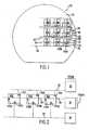
- FIG. 1is a schematic top view of a semiconductor wafer in one embodiment of the present invention.
- FIG. 2shows in enlarged detail a portion of FIG. 1 .
- FIG. 3illustrates linear diffusion in an electroless plating bath.
- FIG. 4illustrates non-linear diffusion in an electroless plating bath.
- FIG. 5is a cross-sectional view of a solid catalytic surface to depict the inhibition reaction mechanism associated with the use of a stabilizer in an electroless plating bath.
- FIG. 6is a schematic top view of a plating bath system for plating multiple wafers.
- a semiconductor wafer 10 fabricated in accordance with an exemplary embodiment of the inventionincludes a substrate 14 on which numerous dice are formed through etching, deposition, and other integrated circuit (IC) fabrication techniques.
- the substrate 14may be formed of a variety of semiconductor materials known in the art including silicon and gallium-arsenide, among others.
- the wafer 10is not limited to any particular size or shape.
- Each wafer 10includes many dice. For clarity of illustration, only dice 18 A-C, 20 A-C, and 22 A-C (collectively “dice 18 - 22 ”) are shown in FIG. 1 .
- the diceare fabricated in the aggregate on wafer 10 , and after fabrication are singulated from wafer 10 using a cutting process, for example. The separation takes place along the areas between adjacent dice, the so-called “street” areas.
- FIG. 2shows a portion of the die 22 in greater detail.
- Small bond padse.g., 70 A, 130 A, 150 A
- the bond padsrequire plating with a conductive metal to form die contacts. Once the bond pad is plated, the die contact is available for subsequent bonding of solder or wire to each die, e.g., 22 A.
- the bond pads/die contacts 70 A, 130 A, 150 Acan be square and measure approximately 5 micrometers ( ⁇ m) or less on a side, although other shapes and dimensions can be used. As stated above, using conventional techniques to plate features having such small dimensions can be difficult. It also is difficult to probe such small features during die testing prior to singulation.
- plating of the small die contacts 70 , 130 , 150 of each dieis promoted by forming conductive connections between the die contacts and a larger supplemental plating structure provided on the wafer 10 .
- each of the die contacts 70 A, 70 B, 70 Cis commonly conductively connected to a larger supplemental plating structure 32 .
- the die contacts 130 A, 130 B, 130 Care conductively connected to a larger supplemental plating structure 34
- die contacts 150 A, 150 B, 150 Care conductively connected to a larger supplemental plating structure 36 .
- Subsequent manufacturing stepsinclude plating the supplemental plating structures at the time the die contacts are plated, which promotes plating of the die contacts 70 A-C, 130 A-C, 150 A-C.
- the supplemental plating structures 26 , 28 , 30 , 32 , 34 , 36also can be used for probe testing the dice prior to singulation.
- the supplemental plating structurese.g., 32 , 34 can be square in shape with each side measuring approximately 100 ⁇ m. Other suitable shapes and dimensions can be used.
- the die contactsare square with a side length of 5 ⁇ m
- the supplemental plating structuresare square with a side length of 100 ⁇ m.
- the surface area of the supplemental plating structureis about 400 times as large as the surface area of a corresponding die contact.
- the supplemental plating structures 26 , 28 , 30 , 32 , 34 , 36are positioned about the wafer 10 such that the total number of dice on wafer 10 either is not reduced at all, or is reduced by a minimum amount by addition of the supplemental plating structures 26 , 28 , 30 , 32 , 34 , 36 .
- the supplemental plating structures 26 , 28 , 30 , 32 , 34 , 36may be placed, for example, along the edge of wafer 10 where there is available space, resulting from the round shape of wafer 10 and the non-round shape of the dice array.
- the supplemental plating structures 26 , 28 , 30 , 32 , 34 , 36may be located in the dicing lanes, i.e., the so-called “street” areas, between the dice.
- FIG. 2also shows conductive paths 52 , 54 , 56 used to connect the supplemental plating structures 26 , 28 , 30 , 32 , 34 , 36 and the die contacts, routed in the streets and on the edges of the wafer 10 .
- the supplemental plating structures 26 , 28 , 30 , 32 , 34 , 36are sacrificed, and subsequently discarded. Also, streets and conductive paths arranged in the streets no longer are needed, and can be cut and discarded.
- conductive paths and supplemental plating structurescan be sacrificed, these sacrificial features may be removed prior to, or at, die singulation. Accordingly, conductive paths and supplemental plating structures can be routed on top of the dice, provided that such routing does not interfere with the plating of the die contacts. Conductive path 54 is shown routed over die 22 in FIG. 2 . Such sacrificial features preferably are removed prior to, or at, singulation, such as by planarization, for example.
- each of the supplemental plating structures 26 , 28 , and 30is connected to two sets of dice (i.e., 18 A-C and 20 A-C).
- other supplemental plating structures 32 , 34 , and 36are connected only to one set of dice (i.e., 22 A-C).
- the number of dice or die contacts connected to a particular supplemental plating structuresis not limited to the illustrated arrangement. In the event that the supplemental plating structures are used as probe pads, however, one particular die contact typically will be connected to one supplemental plating structure. A plurality of die contacts for which probe testing is not necessary can be commonly connected electrically to a single supplemental plating structure of sufficient area to promote plating on the die contacts.
- the wafer 10is subjected to electroless plating.
- an oxidation-reduction reactiontakes place in which suspended metal ions are reduced (i.e., gain electrons) in conjunction with a concomitant oxidation reaction (i.e., a reaction in which electrons are lost).
- the reduced metaldeposits onto a surface, thereby plating the surface.
- the rate of the plating reactionis determined in general by the bath temperature and the chelate concentration (i.e., the free metal concentration).
- the aforementioned plating processis not a diffusion-limited process, and the rate of reaction is independent of the size of the feature to be plated.
- the electroless plating process of the present inventionis a chemical reduction process which depends upon the catalytic reduction of metal ions in an aqueous solution (containing a chemical reducing agent), and the subsequent deposition of metal without the use of electrical energy.
- the driving forceis supplied by the chemical reducing agent in solution.
- FIG. 3shows the supplemental plating structure 32 being subjected to electroless plating in the plating bath 300 .
- the plating bath 300includes a nickel salt, such as, for example, nickel sulfate (NiSO 4 ); a hypophosphite salt, such as, for example, sodium hypophosphite (NaH 2 PO 2 ) or ammonium hypophosphite (NH 4 H 2 PO 2 ); an organic acid or a chelating agent; and a stabilizer, such as, for example, Pb, Cd, or CH 4 N 2 S. Additional possible stabilizers are described below.
- NiSO 4nickel sulfate
- a hypophosphite saltsuch as, for example, sodium hypophosphite (NaH 2 PO 2 ) or ammonium hypophosphite (NH 4 H 2 PO 2 )
- an organic acid or a chelating agentsuch as, for example, Pb, Cd, or CH 4 N 2 S. Additional possible stabilizer
- the hypophosphite saltsare oxidized (i.e., lose electrons) while the Ni 2+ ions contained in the bath are reduced (i.e., gain electrons).
- Ni 2+ ions in the plating bath 300are reduced, and nickel metal is deposited, i.e., plated, on the surface of supplemental plating structure 32 .
- FIG. 4shows the die 22 A having the die contact 70 A being subjected to electroless plating in the plating bath 300 .
- Ni 2+ ions in the plating bath 300are reduced, and nickel metal is deposited, i.e., plated, on the surface of die contact 70 A.
- a metal such as nickelcan catalyze its own reduction. That is, the nickel metal itself has sufficient catalytic activity to oxidize hypophosphite salts such as those used within the bath 300 .
- Such autocatalysisleads to the reduction of nickel ions in the bath, and thus the formation of nickel metal in the bath 300 instead of depositing on the surfaces that are to be plated. Therefore, the aforementioned stabilizer is required to prevent an autocatalytic, “runaway” (i.e., out-of-control) reaction.
- the stabilizeroccupies reactive sites on the nickel surface, thereby physically preventing the solid metal surface from autocatalyzing a runaway reduction reaction.
- the rate of adsorptionis dependent on flow rate and feature size. As flow rate increases, and/or size decreases, the rate of adsorption increases. Thus, the mechanism of an inhibition reaction that uses a stabilizer is diffusion limited and feature size dependent.
- FIG. 5is a cross-sectional view of a solid catalytic surface, and depicts the inhibition reaction mechanism associated with the use of a stabilizer in an electroless plating bath.
- a stabilizer 600(such as Pb) provided in the bath 300 is a surface adsorbing agent that inhibits the electroless reduction reaction by physically occupying various active sites 601 on a solid catalytic surface 602 that could initiate plating, such as the surface of a particle (e.g., nickel, palladium, dust, etc.) in the plating bath.
- a particlee.g., nickel, palladium, dust, etc.
- a stabilizerprevents runaway plating reactions, but at excess concentration levels the stabilizer 600 will occupy too many reactions sites, and will arrest plating in the bath altogether.
- Stabilizerssurface adsorb, and the rate of adsorption is dependent on flow rate and feature size. Adsorption is directly proportional to concentration and flow rate, and is dependent on diffusion mode (i.e., linear or non-linear.) Thus, as the concentration and flow rate of the plating bath increase, the rate of adsorption increases. As a result, small-sized features easily become completely inhibited from plating in a bath with excess stabilizer. Determining the correct stabilizer concentration in a bath is related to the size of the features to be plated. Plating inhibition on smaller features can be reduced by reducing the amount of stabilizer in the solution, but only at the expense of plating bath stability.
- the effective length L 1 of the supplemental plating structure 32is substantially larger than the boundary layer thickness (i.e., diffusion transport distance) ⁇ .
- the boundary layer thicknessi.e., diffusion transport distance
- the radius r associated with die contact 70 Ais of the same approximate magnitude as the distance L 2 . Accordingly, diffusion to the die contacts is non-linear.
- hypophosphite salte.g., NaH 2 PO 2
- catalytically-active particlessuch as palladium or nickel.
- nickel platingonce nickel plating is initiated, plating will continue to occur because the nickel metal itself has sufficient catalytic activity to oxidize hypophosphite salts such as those used within the bath 300 .
- Such runaway platingis undesirable, however, because it can quickly reduce the nickel ions present in the plating bath 300 to particles of nickel metal.
- These nickel particles summed togethercan constitute an enormous amount of surface area, and can destroy the plating bath by combining with the hypophosphite salts rather than diffusing to the surface of the bond pads to be plated.
- the nickel particlescan attach to the sides of the plating tank and associated plumbing. Should a plating bath enter a runaway state, it cannot be used and must be discarded. Also, any remnants of nickel left in the tank would then continue to be catalytic centers for plating in any new plating bath that was placed in the tank. Thus, the tank and plumbing would need to be cleaned in order to purge all nickel remnants from the tank. Such purging generally is done using 20-30% nitric acid.
- the possibility of spontaneous reduction of nickel in the bath 300can be mitigated by the use of stabilizers, such as those discussed above in connection with FIG. 5 .
- the size of the particle that can be neutralizedis generally determined by the concentration of the stabilizer 600 within the bath 300 . As increasing amounts of stabilizer 600 are added to the bath 300 , increasingly larger particles are inhibited, and thus can be prevented from being catalytically active sites. This is true not only for free particles in solution, but also for those areas on the die for which plating is desired.
- the size dependency for conductive areasis related to the linear and non-linear diffusion modes discussed above.
- the size dependency related to diffusion modesmakes for difficulty in effective stabilization of a plating bath to be used for multi-sized surfaces.
- the impact of stabilizer reaching the conductive areasis much greater for small areas than for large areas.
- the amount of stabilizer diffusing to the surface of a conductive area (either large or small) to be platedbecomes sufficiently large, the plating reaction will be chemically inhibited and will cease of its own accord.
- the present inventionsolves the aforementioned and other problems with its ability to plate small features, such as die contacts 70 A-C, yet still have a relatively stable plating bath 300 , by temporarily conductively connecting the bond pads 32 , 34 , 36 to the larger supplemental plating structures as shown in FIG. 2 . Because the die contacts, such as 70 A-C, and supplemental plating structures 32 , 34 , 36 are conductively connected, Ni 2+ is reduced to form the die contact via oxidation of hypophosphite on the supplemental plating structures. Additionally, the plating reaction, once initiated, becomes self-sustaining on both the supplemental plating structures 32 , 34 , 36 and the bond pads/die contacts 70 A-C.
- a typical plating reactiondoes not occur instantly, but requires an initiation process to overcome the reaction threshold. During the time required to complete the initiation there is ample opportunity for stabilizer 600 to diffuse to the surface of an area to be plated and thus inhibit the plating reaction from occurring. Once this initial threshold is overcome and plating is initiated, however, the plating rate is sufficient that the rate of diffusion of stabilizer is insufficient to stop the plating reactions. Given a sufficient supply of plating bath, the plating process reaches completion only when there are no more areas on the surface which can be paired with the nickel ions. In effect, therefore, the plating process does not stop until the wafer is removed from the bath. The nickel ions not used in the plating process remain in the plating bath 300 , but because of the presence of stabilizer 600 , the nickel ions do not react with the hypophosphites.
- the plating bath 300 and electroless deposition processcan be controlled by a system controller 180 .
- Wafers 10 A- 10 Dmay be stacked, one above the other, during plating.
- the system controller 180monitors the stability of the plating bath 300 , and determines the rate at which to inject stabilizers, reducing agent, nickel, and chelating agents into the plating bath 300 .
- the system controller 180can be, for example, a computer.
- the amount of organic acid stabilizeris controlled by maintaining the Ni 2+ concentration in the bath.
- the concentrations of both Ni 2+ and hypophosphite salts in the bath 300are controlled and maintained using an autotitrator that titrates their concentration via feedback control.
- An exemplary way of setting the stabilizer concentrationis to calibrate it based on the feature size being plated.
- stabilizers useful in the present inventioncan include those from the following four categories: compounds of Group VI elements, such as S, Se, and Te; compounds containing oxygen, such as AsO 2 ⁇ , IO 3 ⁇ , and MoO 4 2 ⁇ ; heavy metal cations such as Sn 2+ , Pb 2+ , Hg + , and Sb 3+ ; and unsaturated organic acids, such as maleic acid and itaconic acid.
- the preferred stabilizers for the present inventionare the aforementioned compounds of Group VI elements and heavy metal cations, with the heavy metal cations, and specifically Pb, being most preferred.
Landscapes
- Engineering & Computer Science (AREA)
- Computer Hardware Design (AREA)
- Microelectronics & Electronic Packaging (AREA)
- Power Engineering (AREA)
- Physics & Mathematics (AREA)
- Condensed Matter Physics & Semiconductors (AREA)
- General Physics & Mathematics (AREA)
- Manufacturing & Machinery (AREA)
- Chemically Coating (AREA)
Abstract
Description
- The invention relates to apparatus and techniques for plating small surface features of an integrated circuit device.
- As integrated circuit devices become increasingly complex and feature sizes become increasingly smaller, it becomes more difficult to plate conductive metals onto the very fine pitch features. For example, bond pads formed on dies require plating to form die contacts. Improper or incomplete plating of the bond pads results in die contacts having poor solderability, which decreases yield. Also, it can be difficult to maintain the stability of baths in which parts of various sizes are plated. Consequently, a system for plating small die features, using a stable plating bath, is desired.
- The present invention provides an integrated circuit plating apparatus having a bath for plating die contacts on wafers. Prior to plating, die contacts are conductively connected to larger supplemental plating structures on the wafer. Initiating a plating reaction on the larger supplemental plating structures inductively activates plating on the smaller die contacts. The supplemental plating structures are sacrificed during subsequent processing. Advantageously, the supplemental plating structures also can be used for probe testing prior to die singulation.
- The invention further provides a method of plating die contacts of a plurality of dice (chips) on a wafer, which includes fabricating the larger supplemental plating structures on the wafer, fabricating a conductive connection between the supplemental plating structures and the die contacts, maintaining a plating bath, inserting the wafer into the plating bath, and plating the supplemental plating structures and die contacts. Plating of the die contacts is induced as a result of the conductive connection to the supplemental plating structures. The method and apparatus facilitate the plating of a small contact feature of a wafer die while providing a relatively stable plating bath.
- These and other features of the invention will be seen more clearly from the following detailed description of the invention which is provided in connection with the accompanying drawings.
FIG. 1 is a schematic top view of a semiconductor wafer in one embodiment of the present invention.FIG. 2 shows in enlarged detail a portion ofFIG. 1 .FIG. 3 illustrates linear diffusion in an electroless plating bath.FIG. 4 illustrates non-linear diffusion in an electroless plating bath.FIG. 5 is a cross-sectional view of a solid catalytic surface to depict the inhibition reaction mechanism associated with the use of a stabilizer in an electroless plating bath.FIG. 6 is a schematic top view of a plating bath system for plating multiple wafers.- Referring to
FIG. 1 , asemiconductor wafer 10 fabricated in accordance with an exemplary embodiment of the invention includes asubstrate 14 on which numerous dice are formed through etching, deposition, and other integrated circuit (IC) fabrication techniques. Thesubstrate 14 may be formed of a variety of semiconductor materials known in the art including silicon and gallium-arsenide, among others. Thewafer 10 is not limited to any particular size or shape. - Each
wafer 10 includes many dice. For clarity of illustration, only dice18A-C,20A-C, and22A-C (collectively “dice18-22”) are shown inFIG. 1 . The dice are fabricated in the aggregate onwafer 10, and after fabrication are singulated fromwafer 10 using a cutting process, for example. The separation takes place along the areas between adjacent dice, the so-called “street” areas. FIG. 2 shows a portion of the die22 in greater detail. Small bond pads, e.g.,70A,130A,150A, are provided on each die. The bond pads require plating with a conductive metal to form die contacts. Once the bond pad is plated, the die contact is available for subsequent bonding of solder or wire to each die, e.g.,22A. The bond pads/die contacts - In accordance with the exemplary embodiment, plating of the small die contacts70,130,150 of each die is promoted by forming conductive connections between the die contacts and a larger supplemental plating structure provided on the
wafer 10. For example, as shown inFIGS. 1 and 2 , each of thedie contacts supplemental plating structure 32. Similarly, the diecontacts supplemental plating structure 34, and diecontacts supplemental plating structure 36. Subsequent manufacturing steps include plating the supplemental plating structures at the time the die contacts are plated, which promotes plating of thedie contacts 70A-C,130A-C,150A-C. Advantageously, thesupplemental plating structures - As shown in
FIG. 2 , the supplemental plating structures, e.g.,32,34 can be square in shape with each side measuring approximately 100 μm. Other suitable shapes and dimensions can be used. In one example, the die contacts are square with a side length of 5 μm, and the supplemental plating structures are square with a side length of 100 μm. In the aforementioned example, the surface area of the supplemental plating structure is about 400 times as large as the surface area of a corresponding die contact. - The
supplemental plating structures wafer 10 such that the total number of dice onwafer 10 either is not reduced at all, or is reduced by a minimum amount by addition of thesupplemental plating structures supplemental plating structures wafer 10 where there is available space, resulting from the round shape ofwafer 10 and the non-round shape of the dice array. In another embodiment, thesupplemental plating structures FIG. 2 also showsconductive paths supplemental plating structures wafer 10. During the singulation process, thesupplemental plating structures - Since the conductive paths and supplemental plating structures can be sacrificed, these sacrificial features may be removed prior to, or at, die singulation. Accordingly, conductive paths and supplemental plating structures can be routed on top of the dice, provided that such routing does not interfere with the plating of the die contacts.
Conductive path 54 is shown routed over die22 inFIG. 2 . Such sacrificial features preferably are removed prior to, or at, singulation, such as by planarization, for example. - Referring again to
FIG. 1 , each of thesupplemental plating structures supplemental plating structures - Once the respective die contacts and supplemental plating structures are conductively connected, the
wafer 10 is subjected to electroless plating. In plating processes in general, an oxidation-reduction reaction takes place in which suspended metal ions are reduced (i.e., gain electrons) in conjunction with a concomitant oxidation reaction (i.e., a reaction in which electrons are lost). The reduced metal deposits onto a surface, thereby plating the surface. In such a plating process, the rate of the plating reaction is determined in general by the bath temperature and the chelate concentration (i.e., the free metal concentration). Thus, the aforementioned plating process is not a diffusion-limited process, and the rate of reaction is independent of the size of the feature to be plated. - The electroless plating process of the present invention is a chemical reduction process which depends upon the catalytic reduction of metal ions in an aqueous solution (containing a chemical reducing agent), and the subsequent deposition of metal without the use of electrical energy. In the electroless plating process, instead of the use of electrical energy as the driving force for the reduction of metal ions and their deposition, the driving force is supplied by the chemical reducing agent in solution.
FIG. 3 shows thesupplemental plating structure 32 being subjected to electroless plating in theplating bath 300. Theplating bath 300 includes a nickel salt, such as, for example, nickel sulfate (NiSO4); a hypophosphite salt, such as, for example, sodium hypophosphite (NaH2PO2) or ammonium hypophosphite (NH4H2PO2); an organic acid or a chelating agent; and a stabilizer, such as, for example, Pb, Cd, or CH4N2S. Additional possible stabilizers are described below. During the plating process, the hypophosphite salts are oxidized (i.e., lose electrons) while the Ni2+ ions contained in the bath are reduced (i.e., gain electrons). During plating, Ni2+ ions in theplating bath 300 are reduced, and nickel metal is deposited, i.e., plated, on the surface ofsupplemental plating structure 32.FIG. 4 shows thedie 22A having thedie contact 70A being subjected to electroless plating in theplating bath 300. During plating, Ni2+ ions in theplating bath 300 are reduced, and nickel metal is deposited, i.e., plated, on the surface ofdie contact 70A.- As discussed in greater detail below, a metal such as nickel can catalyze its own reduction. That is, the nickel metal itself has sufficient catalytic activity to oxidize hypophosphite salts such as those used within the
bath 300. Such autocatalysis leads to the reduction of nickel ions in the bath, and thus the formation of nickel metal in thebath 300 instead of depositing on the surfaces that are to be plated. Therefore, the aforementioned stabilizer is required to prevent an autocatalytic, “runaway” (i.e., out-of-control) reaction. The stabilizer occupies reactive sites on the nickel surface, thereby physically preventing the solid metal surface from autocatalyzing a runaway reduction reaction. Because the stabilizer surface adsorbs, the rate of adsorption is dependent on flow rate and feature size. As flow rate increases, and/or size decreases, the rate of adsorption increases. Thus, the mechanism of an inhibition reaction that uses a stabilizer is diffusion limited and feature size dependent. FIG. 5 is a cross-sectional view of a solid catalytic surface, and depicts the inhibition reaction mechanism associated with the use of a stabilizer in an electroless plating bath. As shown inFIG. 5 , a stabilizer600 (such as Pb) provided in thebath 300 is a surface adsorbing agent that inhibits the electroless reduction reaction by physically occupying variousactive sites 601 on a solidcatalytic surface 602 that could initiate plating, such as the surface of a particle (e.g., nickel, palladium, dust, etc.) in the plating bath.- A stabilizer prevents runaway plating reactions, but at excess concentration levels the
stabilizer 600 will occupy too many reactions sites, and will arrest plating in the bath altogether. Stabilizers surface adsorb, and the rate of adsorption is dependent on flow rate and feature size. Adsorption is directly proportional to concentration and flow rate, and is dependent on diffusion mode (i.e., linear or non-linear.) Thus, as the concentration and flow rate of the plating bath increase, the rate of adsorption increases. As a result, small-sized features easily become completely inhibited from plating in a bath with excess stabilizer. Determining the correct stabilizer concentration in a bath is related to the size of the features to be plated. Plating inhibition on smaller features can be reduced by reducing the amount of stabilizer in the solution, but only at the expense of plating bath stability. - Referring again to
FIG. 3 , the effective length L1of thesupplemental plating structure 32 is substantially larger than the boundary layer thickness (i.e., diffusion transport distance) δ. As a result, linear diffusion of stabilizer takes place on the supplemental plating structures. By contrast, referring toFIG. 4 , the radius r associated withdie contact 70A is of the same approximate magnitude as the distance L2. Accordingly, diffusion to the die contacts is non-linear. - It is important to note that the oxidation of a hypophosphite salt (e.g., NaH2PO2) can only occur with catalytically-active particles, such as palladium or nickel. As noted above, once nickel plating is initiated, plating will continue to occur because the nickel metal itself has sufficient catalytic activity to oxidize hypophosphite salts such as those used within the
bath 300. Such runaway plating is undesirable, however, because it can quickly reduce the nickel ions present in theplating bath 300 to particles of nickel metal. These nickel particles summed together can constitute an enormous amount of surface area, and can destroy the plating bath by combining with the hypophosphite salts rather than diffusing to the surface of the bond pads to be plated. - In addition, the nickel particles can attach to the sides of the plating tank and associated plumbing. Should a plating bath enter a runaway state, it cannot be used and must be discarded. Also, any remnants of nickel left in the tank would then continue to be catalytic centers for plating in any new plating bath that was placed in the tank. Thus, the tank and plumbing would need to be cleaned in order to purge all nickel remnants from the tank. Such purging generally is done using 20-30% nitric acid.
- The possibility of spontaneous reduction of nickel in the
bath 300 can be mitigated by the use of stabilizers, such as those discussed above in connection withFIG. 5 . The size of the particle that can be neutralized is generally determined by the concentration of thestabilizer 600 within thebath 300. As increasing amounts ofstabilizer 600 are added to thebath 300, increasingly larger particles are inhibited, and thus can be prevented from being catalytically active sites. This is true not only for free particles in solution, but also for those areas on the die for which plating is desired. The size dependency for conductive areas is related to the linear and non-linear diffusion modes discussed above. - The size dependency related to diffusion modes makes for difficulty in effective stabilization of a plating bath to be used for multi-sized surfaces. The impact of stabilizer reaching the conductive areas is much greater for small areas than for large areas. Once the amount of stabilizer diffusing to the surface of a conductive area (either large or small) to be plated becomes sufficiently large, the plating reaction will be chemically inhibited and will cease of its own accord. Thus, in a given plating bath it may be possible to plate areas measuring 100 μm on a side, but not those measuring 30 μm on a side. Accordingly, a compromise exists between overall bath stability and the size of the conductive area to be plated.
- The present invention solves the aforementioned and other problems with its ability to plate small features, such as die
contacts 70A-C, yet still have a relativelystable plating bath 300, by temporarily conductively connecting thebond pads FIG. 2 . Because the die contacts, such as70A-C, andsupplemental plating structures supplemental plating structures contacts 70A-C. - A typical plating reaction does not occur instantly, but requires an initiation process to overcome the reaction threshold. During the time required to complete the initiation there is ample opportunity for
stabilizer 600 to diffuse to the surface of an area to be plated and thus inhibit the plating reaction from occurring. Once this initial threshold is overcome and plating is initiated, however, the plating rate is sufficient that the rate of diffusion of stabilizer is insufficient to stop the plating reactions. Given a sufficient supply of plating bath, the plating process reaches completion only when there are no more areas on the surface which can be paired with the nickel ions. In effect, therefore, the plating process does not stop until the wafer is removed from the bath. The nickel ions not used in the plating process remain in theplating bath 300, but because of the presence ofstabilizer 600, the nickel ions do not react with the hypophosphites. - As shown in
FIG. 6 , theplating bath 300 and electroless deposition process can be controlled by asystem controller 180.Wafers 10A-10D may be stacked, one above the other, during plating. Thesystem controller 180 monitors the stability of theplating bath 300, and determines the rate at which to inject stabilizers, reducing agent, nickel, and chelating agents into theplating bath 300. Thesystem controller 180 can be, for example, a computer. Typically, the amount of organic acid stabilizer is controlled by maintaining the Ni2+ concentration in the bath. In the present invention, the concentrations of both Ni2+ and hypophosphite salts in thebath 300 are controlled and maintained using an autotitrator that titrates their concentration via feedback control. An exemplary way of setting the stabilizer concentration is to calibrate it based on the feature size being plated. - Various stabilizers can be used in
bath 300 in accordance with the present invention. Generally, stabilizers useful in the present invention can include those from the following four categories: compounds of Group VI elements, such as S, Se, and Te; compounds containing oxygen, such as AsO2−, IO3−, and MoO42−; heavy metal cations such as Sn2+, Pb2+, Hg+, and Sb3+; and unsaturated organic acids, such as maleic acid and itaconic acid. Typically, the preferred stabilizers for the present invention are the aforementioned compounds of Group VI elements and heavy metal cations, with the heavy metal cations, and specifically Pb, being most preferred. - While the invention has been described and illustrated with reference to specific exemplary embodiments, it should be understood that many modifications and substitutions can be made without departing from the spirit and scope of the invention. Accordingly, the invention is not to be considered as limited by the foregoing description but is only limited by the scope of the appended claims.
Claims (21)
Priority Applications (1)
| Application Number | Priority Date | Filing Date | Title |
|---|---|---|---|
| US13/079,364US8431484B2 (en) | 2003-07-21 | 2011-04-04 | Stable electroless fine pitch interconnect plating |
Applications Claiming Priority (3)
| Application Number | Priority Date | Filing Date | Title |
|---|---|---|---|
| US10/622,497US7052922B2 (en) | 2003-07-21 | 2003-07-21 | Stable electroless fine pitch interconnect plating |
| US11/402,924US20060180461A1 (en) | 2003-07-21 | 2006-04-13 | Stable electroless fine pitch interconnect plating |
| US13/079,364US8431484B2 (en) | 2003-07-21 | 2011-04-04 | Stable electroless fine pitch interconnect plating |
Related Parent Applications (1)
| Application Number | Title | Priority Date | Filing Date |
|---|---|---|---|
| US11/402,924ContinuationUS20060180461A1 (en) | 2003-07-21 | 2006-04-13 | Stable electroless fine pitch interconnect plating |
Publications (2)
| Publication Number | Publication Date |
|---|---|
| US20110183514A1true US20110183514A1 (en) | 2011-07-28 |
| US8431484B2 US8431484B2 (en) | 2013-04-30 |
Family
ID=34079756
Family Applications (3)
| Application Number | Title | Priority Date | Filing Date |
|---|---|---|---|
| US10/622,497Expired - LifetimeUS7052922B2 (en) | 2003-07-21 | 2003-07-21 | Stable electroless fine pitch interconnect plating |
| US11/402,924AbandonedUS20060180461A1 (en) | 2003-07-21 | 2006-04-13 | Stable electroless fine pitch interconnect plating |
| US13/079,364Expired - Fee RelatedUS8431484B2 (en) | 2003-07-21 | 2011-04-04 | Stable electroless fine pitch interconnect plating |
Family Applications Before (2)
| Application Number | Title | Priority Date | Filing Date |
|---|---|---|---|
| US10/622,497Expired - LifetimeUS7052922B2 (en) | 2003-07-21 | 2003-07-21 | Stable electroless fine pitch interconnect plating |
| US11/402,924AbandonedUS20060180461A1 (en) | 2003-07-21 | 2006-04-13 | Stable electroless fine pitch interconnect plating |
Country Status (1)
| Country | Link |
|---|---|
| US (3) | US7052922B2 (en) |
Families Citing this family (6)
| Publication number | Priority date | Publication date | Assignee | Title |
|---|---|---|---|---|
| JP2006318966A (en)* | 2005-05-10 | 2006-11-24 | Disco Abrasive Syst Ltd | Semiconductor wafer |
| US20080149490A1 (en)* | 2006-12-26 | 2008-06-26 | Bonhote Christian R | Electroplating on ultra-thin seed layers |
| US8021535B2 (en)* | 2007-12-26 | 2011-09-20 | Hitachi Global Storage Technologies Netherlands B.V. | Methods for plating write pole shield structures with ultra-thin metal gap seed layers |
| CN102334229A (en)* | 2009-02-25 | 2012-01-25 | 东京毅力科创株式会社 | Dye adsorption method and adsorption device of photosensitizing dye, manufacturing method and adsorption device of dye-sensitized solar cell, and dye-sensitized solar cell |
| US8569167B2 (en) | 2011-03-29 | 2013-10-29 | Micron Technology, Inc. | Methods for forming a semiconductor structure |
| US10037925B2 (en) | 2016-03-04 | 2018-07-31 | Qorvo Us, Inc. | Removable sacrificial connections for semiconductor devices |
Citations (18)
| Publication number | Priority date | Publication date | Assignee | Title |
|---|---|---|---|---|
| US5209817A (en)* | 1991-08-22 | 1993-05-11 | International Business Machines Corporation | Selective plating method for forming integral via and wiring layers |
| US5260220A (en)* | 1991-11-19 | 1993-11-09 | Arco Chemical Technology, L.P. | Method and apparatus for monitoring impurities in a liquified hydrocarbon stream |
| US5484626A (en)* | 1992-04-06 | 1996-01-16 | Shipley Company L.L.C. | Methods and apparatus for maintaining electroless plating solutions |
| US5972116A (en)* | 1994-12-29 | 1999-10-26 | F.T.I. Co., Ltd. | Method and apparatus for producing a semiconductor device |
| US5994915A (en)* | 1996-09-13 | 1999-11-30 | Micron Technology, Inc. | Reduced terminal testing system |
| US6060176A (en)* | 1995-11-30 | 2000-05-09 | International Business Machines Corporation | Corrosion protection for metallic features |
| US6245389B1 (en)* | 1996-12-27 | 2001-06-12 | Nippon Chemical Industrial Co., Ltd. | Method for circulating electroless nickel plating solution |
| US6335626B1 (en)* | 1997-08-21 | 2002-01-01 | Pac Tech - Packaging Technologies Gmbh | Method and device for determining a parameter for a metallization bath |
| US6350633B1 (en)* | 2000-08-22 | 2002-02-26 | Charles W. C. Lin | Semiconductor chip assembly with simultaneously electroplated contact terminal and connection joint |
| US6362089B1 (en)* | 1999-04-19 | 2002-03-26 | Motorola, Inc. | Method for processing a semiconductor substrate having a copper surface disposed thereon and structure formed |
| US6505634B2 (en)* | 2001-03-23 | 2003-01-14 | Will Be S & T Co., Ltd. | Semiconductor wafer cleaning apparatus |
| US20030219976A1 (en)* | 2002-05-24 | 2003-11-27 | Jeffery N. Gleason | Using stabilizers in electroless solutions to inhibit plating of fuses |
| US6660626B1 (en)* | 2000-08-22 | 2003-12-09 | Charles W. C. Lin | Semiconductor chip assembly with simultaneously electrolessly plated contact terminal and connection joint |
| US6709561B1 (en)* | 2002-11-06 | 2004-03-23 | Eci Technology, Inc. | Measurement of the concentration of a reducing agent in an electroless plating bath |
| US6764879B2 (en)* | 2001-08-08 | 2004-07-20 | Matsushita Electric Industrial Co., Ltd. | Semiconductor wafer, semiconductor device, and method for manufacturing the same |
| US6774039B1 (en)* | 2002-08-08 | 2004-08-10 | Novellus Systems, Inc. | Process scheme for improving electroplating performance in integrated circuit manufacture |
| US6841476B1 (en)* | 1999-09-27 | 2005-01-11 | Citizen Watch Co., Ltd. | Electroless plating method |
| US6953951B2 (en)* | 2000-12-11 | 2005-10-11 | Semiconductor Energy Laboratory Co., Ltd. | Semiconductor device, and manufacturing method thereof |
- 2003
- 2003-07-21USUS10/622,497patent/US7052922B2/ennot_activeExpired - Lifetime
- 2006
- 2006-04-13USUS11/402,924patent/US20060180461A1/ennot_activeAbandoned
- 2011
- 2011-04-04USUS13/079,364patent/US8431484B2/ennot_activeExpired - Fee Related
Patent Citations (19)
| Publication number | Priority date | Publication date | Assignee | Title |
|---|---|---|---|---|
| US5209817A (en)* | 1991-08-22 | 1993-05-11 | International Business Machines Corporation | Selective plating method for forming integral via and wiring layers |
| US5260220A (en)* | 1991-11-19 | 1993-11-09 | Arco Chemical Technology, L.P. | Method and apparatus for monitoring impurities in a liquified hydrocarbon stream |
| US5484626A (en)* | 1992-04-06 | 1996-01-16 | Shipley Company L.L.C. | Methods and apparatus for maintaining electroless plating solutions |
| US5972116A (en)* | 1994-12-29 | 1999-10-26 | F.T.I. Co., Ltd. | Method and apparatus for producing a semiconductor device |
| US6060176A (en)* | 1995-11-30 | 2000-05-09 | International Business Machines Corporation | Corrosion protection for metallic features |
| US5994915A (en)* | 1996-09-13 | 1999-11-30 | Micron Technology, Inc. | Reduced terminal testing system |
| US6245389B1 (en)* | 1996-12-27 | 2001-06-12 | Nippon Chemical Industrial Co., Ltd. | Method for circulating electroless nickel plating solution |
| US6335626B1 (en)* | 1997-08-21 | 2002-01-01 | Pac Tech - Packaging Technologies Gmbh | Method and device for determining a parameter for a metallization bath |
| US6362089B1 (en)* | 1999-04-19 | 2002-03-26 | Motorola, Inc. | Method for processing a semiconductor substrate having a copper surface disposed thereon and structure formed |
| US6841476B1 (en)* | 1999-09-27 | 2005-01-11 | Citizen Watch Co., Ltd. | Electroless plating method |
| US6350633B1 (en)* | 2000-08-22 | 2002-02-26 | Charles W. C. Lin | Semiconductor chip assembly with simultaneously electroplated contact terminal and connection joint |
| US6660626B1 (en)* | 2000-08-22 | 2003-12-09 | Charles W. C. Lin | Semiconductor chip assembly with simultaneously electrolessly plated contact terminal and connection joint |
| US6953951B2 (en)* | 2000-12-11 | 2005-10-11 | Semiconductor Energy Laboratory Co., Ltd. | Semiconductor device, and manufacturing method thereof |
| US6505634B2 (en)* | 2001-03-23 | 2003-01-14 | Will Be S & T Co., Ltd. | Semiconductor wafer cleaning apparatus |
| US6764879B2 (en)* | 2001-08-08 | 2004-07-20 | Matsushita Electric Industrial Co., Ltd. | Semiconductor wafer, semiconductor device, and method for manufacturing the same |
| US20030219976A1 (en)* | 2002-05-24 | 2003-11-27 | Jeffery N. Gleason | Using stabilizers in electroless solutions to inhibit plating of fuses |
| US6709980B2 (en)* | 2002-05-24 | 2004-03-23 | Micron Technology, Inc. | Using stabilizers in electroless solutions to inhibit plating of fuses |
| US6774039B1 (en)* | 2002-08-08 | 2004-08-10 | Novellus Systems, Inc. | Process scheme for improving electroplating performance in integrated circuit manufacture |
| US6709561B1 (en)* | 2002-11-06 | 2004-03-23 | Eci Technology, Inc. | Measurement of the concentration of a reducing agent in an electroless plating bath |
Also Published As
| Publication number | Publication date |
|---|---|
| US20060180461A1 (en) | 2006-08-17 |
| US8431484B2 (en) | 2013-04-30 |
| US7052922B2 (en) | 2006-05-30 |
| US20050020064A1 (en) | 2005-01-27 |
Similar Documents
| Publication | Publication Date | Title |
|---|---|---|
| US8431484B2 (en) | Stable electroless fine pitch interconnect plating | |
| JP2024512696A (en) | Direct joining method and structure | |
| US7190052B2 (en) | Semiconductor devices with oxide coatings selectively positioned over exposed features including semiconductor material | |
| US5277756A (en) | Post fabrication processing of semiconductor chips | |
| US6436300B2 (en) | Method of manufacturing electronic components | |
| EP1310988B1 (en) | Method of manufacturing a semiconductor element | |
| TW201438146A (en) | Improved metal to metal bonding for stacked (3D) integrated circuits | |
| US10865484B2 (en) | Solution and method for etching titanium based materials | |
| US6586043B1 (en) | Methods of electroless deposition of nickel, methods of forming under bump metallurgy, and constructions comprising solder bumps | |
| KR20210039179A (en) | Etchant for etching Ti-W film | |
| JP2008502156A (en) | Semiconductor device with reduced contact resistance | |
| EP0479373A1 (en) | Method of manufacturing a semiconductor device by electroless metallisation | |
| US6709980B2 (en) | Using stabilizers in electroless solutions to inhibit plating of fuses | |
| DE102005035772A1 (en) | Contact layer production with contact bumps, e.g. for manufacture of integrated circuits, involves dry-etching process for structuring bump bottom-face metallization layer stack | |
| US7425278B2 (en) | Process of etching a titanium/tungsten surface and etchant used therein | |
| US12074096B2 (en) | Die attach surface copper layer with protective layer for microelectronic devices | |
| US20050085062A1 (en) | Processes and tools for forming lead-free alloy solder precursors | |
| JP4551229B2 (en) | Semiconductor device manufacturing method and etching solution | |
| US20040011991A1 (en) | Use of a gettering agent in a chemical mechanical polishing and rinsing operation and apparatus therefor | |
| EP3712298A1 (en) | Semiconductor substrate and manufacturing method therefor | |
| US20230077737A1 (en) | Diffusion layers in metal interconnects | |
| US20060169751A1 (en) | Method for depositing an adhesion-promoting layer on a metallic layer of a chip | |
| Chen et al. | Electroless nickel bath for wafer bumping: Influence of additives | |
| US20240218519A1 (en) | Electroless plating with a floating potential | |
| JP3335883B2 (en) | Manufacturing method of bump electrode |
Legal Events
| Date | Code | Title | Description |
|---|---|---|---|
| FEPP | Fee payment procedure | Free format text:PAYOR NUMBER ASSIGNED (ORIGINAL EVENT CODE: ASPN); ENTITY STATUS OF PATENT OWNER: LARGE ENTITY | |
| AS | Assignment | Owner name:U.S. BANK NATIONAL ASSOCIATION, AS COLLATERAL AGENT, CALIFORNIA Free format text:SECURITY INTEREST;ASSIGNOR:MICRON TECHNOLOGY, INC.;REEL/FRAME:038669/0001 Effective date:20160426 Owner name:U.S. BANK NATIONAL ASSOCIATION, AS COLLATERAL AGEN Free format text:SECURITY INTEREST;ASSIGNOR:MICRON TECHNOLOGY, INC.;REEL/FRAME:038669/0001 Effective date:20160426 | |
| AS | Assignment | Owner name:MORGAN STANLEY SENIOR FUNDING, INC., AS COLLATERAL AGENT, MARYLAND Free format text:PATENT SECURITY AGREEMENT;ASSIGNOR:MICRON TECHNOLOGY, INC.;REEL/FRAME:038954/0001 Effective date:20160426 Owner name:MORGAN STANLEY SENIOR FUNDING, INC., AS COLLATERAL Free format text:PATENT SECURITY AGREEMENT;ASSIGNOR:MICRON TECHNOLOGY, INC.;REEL/FRAME:038954/0001 Effective date:20160426 | |
| REMI | Maintenance fee reminder mailed | ||
| LAPS | Lapse for failure to pay maintenance fees | ||
| STCH | Information on status: patent discontinuation | Free format text:PATENT EXPIRED DUE TO NONPAYMENT OF MAINTENANCE FEES UNDER 37 CFR 1.362 | |
| AS | Assignment | Owner name:U.S. BANK NATIONAL ASSOCIATION, AS COLLATERAL AGENT, CALIFORNIA Free format text:CORRECTIVE ASSIGNMENT TO CORRECT THE REPLACE ERRONEOUSLY FILED PATENT #7358718 WITH THE CORRECT PATENT #7358178 PREVIOUSLY RECORDED ON REEL 038669 FRAME 0001. ASSIGNOR(S) HEREBY CONFIRMS THE SECURITY INTEREST;ASSIGNOR:MICRON TECHNOLOGY, INC.;REEL/FRAME:043079/0001 Effective date:20160426 Owner name:U.S. BANK NATIONAL ASSOCIATION, AS COLLATERAL AGEN Free format text:CORRECTIVE ASSIGNMENT TO CORRECT THE REPLACE ERRONEOUSLY FILED PATENT #7358718 WITH THE CORRECT PATENT #7358178 PREVIOUSLY RECORDED ON REEL 038669 FRAME 0001. ASSIGNOR(S) HEREBY CONFIRMS THE SECURITY INTEREST;ASSIGNOR:MICRON TECHNOLOGY, INC.;REEL/FRAME:043079/0001 Effective date:20160426 | |
| FP | Lapsed due to failure to pay maintenance fee | Effective date:20170430 | |
| AS | Assignment | Owner name:MICRON TECHNOLOGY, INC., IDAHO Free format text:RELEASE BY SECURED PARTY;ASSIGNOR:U.S. BANK NATIONAL ASSOCIATION, AS COLLATERAL AGENT;REEL/FRAME:047243/0001 Effective date:20180629 | |
| AS | Assignment | Owner name:MICRON TECHNOLOGY, INC., IDAHO Free format text:RELEASE BY SECURED PARTY;ASSIGNOR:MORGAN STANLEY SENIOR FUNDING, INC., AS COLLATERAL AGENT;REEL/FRAME:050937/0001 Effective date:20190731 |