US20110179218A1 - Method for reading a multilevel cell in a non-volatile memory device - Google Patents
Method for reading a multilevel cell in a non-volatile memory deviceDownload PDFInfo
- Publication number
- US20110179218A1 US20110179218A1US13/073,317US201113073317AUS2011179218A1US 20110179218 A1US20110179218 A1US 20110179218A1US 201113073317 AUS201113073317 AUS 201113073317AUS 2011179218 A1US2011179218 A1US 2011179218A1
- Authority
- US
- United States
- Prior art keywords
- data
- read
- upper page
- memory
- latch
- Prior art date
- Legal status (The legal status is an assumption and is not a legal conclusion. Google has not performed a legal analysis and makes no representation as to the accuracy of the status listed.)
- Granted
Links
Images


Classifications
- G—PHYSICS
- G06—COMPUTING OR CALCULATING; COUNTING
- G06F—ELECTRIC DIGITAL DATA PROCESSING
- G06F12/00—Accessing, addressing or allocating within memory systems or architectures
- G06F12/02—Addressing or allocation; Relocation
- G06F12/0223—User address space allocation, e.g. contiguous or non contiguous base addressing
- G06F12/023—Free address space management
- G06F12/0238—Memory management in non-volatile memory, e.g. resistive RAM or ferroelectric memory
- G06F12/0246—Memory management in non-volatile memory, e.g. resistive RAM or ferroelectric memory in block erasable memory, e.g. flash memory
- G—PHYSICS
- G11—INFORMATION STORAGE
- G11C—STATIC STORES
- G11C16/00—Erasable programmable read-only memories
- G11C16/02—Erasable programmable read-only memories electrically programmable
- G11C16/06—Auxiliary circuits, e.g. for writing into memory
- G11C16/26—Sensing or reading circuits; Data output circuits
- G—PHYSICS
- G11—INFORMATION STORAGE
- G11C—STATIC STORES
- G11C11/00—Digital stores characterised by the use of particular electric or magnetic storage elements; Storage elements therefor
- G11C11/56—Digital stores characterised by the use of particular electric or magnetic storage elements; Storage elements therefor using storage elements with more than two stable states represented by steps, e.g. of voltage, current, phase, frequency
- G11C11/5621—Digital stores characterised by the use of particular electric or magnetic storage elements; Storage elements therefor using storage elements with more than two stable states represented by steps, e.g. of voltage, current, phase, frequency using charge storage in a floating gate
- G11C11/5642—Sensing or reading circuits; Data output circuits
- G—PHYSICS
- G11—INFORMATION STORAGE
- G11C—STATIC STORES
- G11C16/00—Erasable programmable read-only memories
- G11C16/02—Erasable programmable read-only memories electrically programmable
- G11C16/04—Erasable programmable read-only memories electrically programmable using variable threshold transistors, e.g. FAMOS
- G11C16/0483—Erasable programmable read-only memories electrically programmable using variable threshold transistors, e.g. FAMOS comprising cells having several storage transistors connected in series
- G—PHYSICS
- G11—INFORMATION STORAGE
- G11C—STATIC STORES
- G11C16/00—Erasable programmable read-only memories
- G11C16/02—Erasable programmable read-only memories electrically programmable
- G11C16/06—Auxiliary circuits, e.g. for writing into memory
- G—PHYSICS
- G11—INFORMATION STORAGE
- G11C—STATIC STORES
- G11C2211/00—Indexing scheme relating to digital stores characterized by the use of particular electric or magnetic storage elements; Storage elements therefor
- G11C2211/56—Indexing scheme relating to G11C11/56 and sub-groups for features not covered by these groups
- G11C2211/564—Miscellaneous aspects
- G11C2211/5641—Multilevel memory having cells with different number of storage levels
- G—PHYSICS
- G11—INFORMATION STORAGE
- G11C—STATIC STORES
- G11C2211/00—Indexing scheme relating to digital stores characterized by the use of particular electric or magnetic storage elements; Storage elements therefor
- G11C2211/56—Indexing scheme relating to G11C11/56 and sub-groups for features not covered by these groups
- G11C2211/564—Miscellaneous aspects
- G11C2211/5643—Multilevel memory comprising cache storage devices
- G—PHYSICS
- G11—INFORMATION STORAGE
- G11C—STATIC STORES
- G11C2211/00—Indexing scheme relating to digital stores characterized by the use of particular electric or magnetic storage elements; Storage elements therefor
- G11C2211/56—Indexing scheme relating to G11C11/56 and sub-groups for features not covered by these groups
- G11C2211/564—Miscellaneous aspects
- G11C2211/5646—Multilevel memory with flag bits, e.g. for showing that a "first page" of a word line is programmed but not a "second page"
Definitions
- the present inventionrelates generally to memory devices and in particular the present invention relates to non-volatile memory devices.
- RAMrandom-access memory
- ROMread only memory
- DRAMdynamic random access memory
- SDRAMsynchronous dynamic random access memory
- flash memoryflash memory
- Flash memory deviceshave developed into a popular source of non-volatile memory for a wide range of electronic applications. Flash memory devices typically use a one-transistor memory cell that allows for high memory densities, high reliability, and low power consumption. Common uses for flash memory include personal computers, personal digital assistants (PDAs), digital cameras, and cellular telephones. Program code and system data such as a basic input/output system (BIOS) are typically stored in flash memory devices for use in personal computer systems.
- BIOSbasic input/output system
- Memory densitycan be increased by using multiple level cells (MLC) instead of single level cells (SLC).
- MLC memorycan increase the amount of data stored in an integrated circuit without adding additional cells and/or increasing the size of the die.
- the MLC methodstores two or more data bits in each memory cell.
- FIG. 1illustrates a typical prior art SLC NAND memory cell array.
- This figureshows a 16 k bit line and 32 word line memory array as used in a typical 2 kilobyte (kB) memory block.
- the arrayis comprised of word lines WL 0 -WL 31 and bit lines BL 0 -BL 16383 .
- Select gate drain (SGD) transistors 101 , 102 and select gate source (SGS) transistors 104 , 105are used on each end of each bit line to enable selective access to the array.
- a source line 100is coupled to the source end of the serial bit lines.
- Each word line of the SLC arrayis considered to be a page of data.
- WL 0can be considered to be page 0 with 2 kB of data.
- WL 1is then page 1. This continues up to WL 31 that is labeled page 31.
- FIG. 2illustrates a typical prior art MLC NAND memory cell array. This figure shows basically the same architecture as the SLC array including bit lines BL 0 -BL 16383 , WL 0 -WL 31 , the SGD transistors 201 , 202 , SGS transistors 204 , 205 , and the source line 200 .
- the MLC memory arrayis comprised of 63 pages of data since is has two bits for each memory cell.
- Each word line WL 0 -WL 31 of the MLC arrayis comprised of two pages of data.
- WL 0is page 0 and page 1 that is equal to 4 kB of data. This continues up to WL 31 that is comprised of page 62 and page 63.
- the lower pagesare even pages page 0, page 2, . . . page 62.
- the upper page dataare the odd pages page 1, page 3, . . . page 63.
- the memory controllertypically first sends the lower page data for programming then the upper page data is programmed.
- a multilevel cellhas multiple threshold voltage (V t ) windows that each indicates a different state.
- FIG. 3illustrates a typical MLC V t distribution for lower page and upper page data.
- Multilevel cellstake advantage of the analog nature of a traditional flash cell by assigning a bit pattern to a specific voltage range stored on the cell. This technology permits the storage of two or more bits per cell, depending on the quantity of voltage ranges assigned to the cell.
- FIG. 3shows that the lower page of data V t is comprised of one of two states only (i.e., “11” or “10”) where the right-most bit is considered to be the lower page of data.
- the “11” stateis typically referred to as the erased state.
- the rLP voltage indicated along the V t axisis the lower page read bias that is applied to the selected word line.
- An unselected word line voltageis approximately 5.5V to bypass the even upper cell states.
- the rLP voltageis typically around 0.5V.
- the lower distribution of FIG. 3is the upper page cell V t distribution.
- the upper page datais written to the cells already programmed with the lower page of data.
- the arrows from the lower page V t distribution to the upper page V t distributionshows the possible changes in state.
- the erase state, “11”can become a logical “11” 301 after a logical “1” is programmed into the upper page of data or it can become a logical “01” 302 after the upper page of data is programmed as a logical “0”.
- the lower page programmed state of “10”can either become a logical “00” 305 after the upper page of data is programmed as a logical “0” state or it can become a “10” 306 after the upper page is programmed as a logical “1”.
- the voltage r00is illustrated along the V t axis.
- the r00 voltageis the voltage used to bias the word lines in order to read the lower data when the upper data has been written.
- r00is 1.3V.
- the upper page datais written for the selected word line.
- the upper page datais not written for the selected word line. Therefore, it is necessary to have information available to determine whether the selected word line has had the upper page cell data written.
- MLC flash memory devicestypically use flag data stored in a flag data cell to indicate to the internal controller inside the flash memory whether the upper page is written or not for the selected word line.
- the flag datais used by the internal controller inside the flash memory to decide the internal read algorithm. If the flag data shows the upper page is not written, only the lower page is written so that the lower page read needs to be executed further to read correct data. If the flag data shows the upper page data is not written, the already read data is the correct data. Therefore, there is no need for a further read operation. Reading the flag data can cause a data cache busy indicator to indicate, during worst case conditions, that the cache is busy during a time when a lower page read voltage needs to be generated in an MLC device. This can cause a conflict during lower page access in an MLC device.
- FIG. 1shows a typical prior art single level cell memory array architecture.
- FIG. 2shows a typical prior art multiple level cell memory array architecture.
- FIG. 3shows a typical prior art threshold voltage distribution.
- FIG. 4shows a block diagram of one embodiment of the structures of the flash memory array, flag memory array, and page buffers.
- FIG. 5shows a simplified block diagram of a page buffer function.
- FIG. 6shows a flow chart of a typical prior art lower page read operation.
- FIG. 7shows one embodiment of lower page read process of the present invention.
- FIG. 8shows a block diagram of one embodiment of a memory system of the present invention.
- FIG. 9shows a block diagram of one embodiment of a memory module of the present invention.
- FIG. 4illustrates a block diagram of one embodiment of a memory device including the flash memory array, flag memory cell array, and page buffers. This figure shows the main memory array 400 coupled to a flag memory cell array 403 .
- the flag memory cell arraystores the flag data that provides the indication as to whether each main memory array 400 cell is an MLC memory or an SLC memory.
- the array blocks 400 , 403are coupled to a page buffer cache block 405 through a wired multiplexer 404 .
- the page buffer cache 405temporarily stores data that is being written to or read from the arrays 400 , 403 in order to increase the read and write speeds of the memory device.
- the page buffer 405includes a sense amplifier circuit, a data latch, and a cache latch for memory operation.
- the flag memory cell array 403provides a record of how a memory cell has been programmed. When the upper page data is programmed, the flag memory cell associated with that page is also programmed. When lower page data is read, the associated flag memory cell is also read. This flag cell information is used to determine how to proceed during a lower page read algorithm.
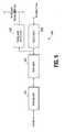
- FIG. 5illustrates a simplified block diagram of one embodiment of a page buffer function.
- the MLC page buffer 405includes a sensing circuit 501 and a data latch 502 that stores sensed data during a read operation.
- Data to be programmed during a programming operationis also stored in the data latch 502 .
- the cache latch 505stores the data that is read before being output to the output multiplexer of the memory device during a read operation.
- Additional latches 506are coupled to a verify-path wired NOR line.
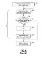
- FIG. 6illustrates a flowchart of a typical prior art method for a lower page read operation.
- the procedureis comprised of sensing the memory cell and storing the sensed data in the data latch 601 .
- the read voltage r00is used during the read operation.
- the datais then transferred from the data latch to the cache latch 603 .
- the flag cellis then checked 605 from the output of the cache latch of the flag page buffer. If the flag has been set, upper page data of MLC data has been read and the data is ready to be read from the cache latch 610 . If the flag is not set, the rLP voltage is applied to the selected word line 607 in order to read the lower page of data.
- the datais then transferred from the data latch to the cache latch 609 .
- the datais then read out from the cache latch 610 .
- cache latch datai.e., previous read data
- the readingis resumed after the user access to the cache latch has been completed.
- the prior art methoddoes not allow background reading to occur since the flag data cell check is coming from the cache latch data.
- FIG. 7illustrates a flow chart of one embodiment of the method of the present invention for performing a lower page read operation.
- the method of FIG. 7should be read in conjunction with the block diagram of FIG. 5 that illustrates the data and cache latches.
- the selected memory cellis biased at a read voltage r00 and the resulting read data is sensed 701 .
- the datais stored in the data latch 701 .
- the flag datais checked for the read data 703 .
- the flagis either a logical “1” state or a logical “0” state to provide an indication.
- the flag cellis written from the data latch of the flag page buffer. If the flag is indicating that lower page data been read, the data is transferred from the data latch to the cache latch 707 . The data is then read out of the cache latch 709 .
- the selected word lineis biased at the rLP voltage 705 (e.g., 0V to 0.8V) in order to read the lower page of data. This can be accomplished by turning on a voltage pump to generate the appropriate voltage.
- the datais then transferred from the data latch to the cache latch 707 .
- the datais now ready to be read out from the cache latch 709 .
- the lower page read procedure of the present inventiongreatly improves read data throughput. This is accomplished without affecting the cache data, that is being accessed by the user, from a previous read of the latched data.
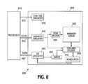
- FIG. 8illustrates a functional block diagram of a memory device 800 that can incorporate the flash memory array and programming method embodiments of the present invention.
- the memory device 800is coupled to a processor 810 .
- the processor 810may be a microprocessor or some other type of controlling circuitry.
- the memory device 800 and the processor 810form part of a memory system 820 .
- the memory device 800has been simplified to focus on features of the memory that are helpful in understanding the present invention.
- the memory deviceincludes an array of flash memory cells 830 as described above with reference to FIG. 8 .
- the memory array 830is arranged in banks of rows and columns.
- the control gates of each row of memory cellsis coupled with a word line while the drain and source connections of the memory cells are coupled to bitlines.
- the connections of the cells to the bitlinesdetermines whether the array is a NAND architecture, an AND architecture, or a NOR architecture.
- An address buffer circuit 840is provided to latch address signals provided on address input connections A 0 -Ax 842 . Address signals are received and decoded by a row decoder 844 and a column decoder 846 to access the memory array 830 . It will be appreciated by those skilled in the art, with the benefit of the present description, that the number of address input connections depends on the density and architecture of the memory array 830 . That is, the number of addresses increases with both increased memory cell counts and increased bank and block counts.
- the memory device 800reads data in the memory array 830 by sensing voltage or current changes in the memory array columns using sense/buffer circuitry 850 .
- the sense/buffer circuitryin one embodiment, is coupled to read and latch a row of data from the memory array 830 .
- Data input and output buffer circuitry 860is included for bi-directional data communication over a plurality of data connections 862 with the controller 810 .
- Write circuitry 855is provided to write data to the memory array.
- Control circuitry 870decodes signals provided on control connections 872 from the processor 810 . These signals are used to control the operations on the memory array 830 , including data read, data write (program), and erase operations.
- the control circuitry 870may be a state machine, a sequencer, or some other type of controller. In one embodiment, the control circuitry 870 executes the embodiments of the lower page read method of the present invention.
- the flash memory device illustrated in FIG. 8has been simplified to facilitate a basic understanding of the features of the memory. A more detailed understanding of internal circuitry and functions of flash memories are known to those skilled in the art.
- FIG. 9is an illustration of an exemplary memory module 900 .
- Memory module 900is illustrated as a memory card, although the concepts discussed with reference to memory module 900 are applicable to other types of removable or portable memory, e.g., USB flash drives, and are intended to be within the scope of “memory module” as used herein.
- memory modulee.g., USB flash drives
- FIG. 9shows one example form factor, these concepts are applicable to other form factors as well.
- memory module 900will include a housing 905 (as depicted) to enclose one or more memory devices 910 , though such a housing is not essential to all devices or device applications. At least one memory device 910 is a non-volatile memory [including or adapted to perform elements of the invention].
- the housing 905includes one or more contacts 915 for communication with a host device. Examples of host devices include digital cameras, digital recording and playback devices, PDAs, personal computers, memory card readers, interface hubs and the like.
- the contacts 915are in the form of a standardized interface. For example, with a USB flash drive, the contacts 915 might be in the form of a USB Type-A male connector.
- the contacts 915are in the form of a semi-proprietary interface, such as might be found on COMPACTFLASH memory cards licensed by SANDISK Corporation, MEMORYSTICK memory cards licensed by SONY Corporation, SD SECURE DIGITAL memory cards licensed by TOSHIBA Corporation and the like. In general, however, contacts 915 provide an interface for passing control, address and/or data signals between the memory module 900 and a host having compatible receptors for the contacts 915 .
- the memory module 900may optionally include additional circuitry 920 which may be one or more integrated circuits and/or discrete components.
- the additional circuitry 920may include a memory controller for controlling access across multiple memory devices 910 and/or for providing a translation layer between an external host and a memory device 910 .
- a memory controllercould selectively couple an I/O connection (not shown in FIG. 9 ) of a memory device 910 to receive the appropriate signal at the appropriate I/O connection at the appropriate time or to provide the appropriate signal at the appropriate contact 915 at the appropriate time.
- the communication protocol between a host and the memory module 900may be different than what is required for access of a memory device 910 .
- a memory controllercould then translate the command sequences received from a host into the appropriate command sequences to achieve the desired access to the memory device 910 .
- Such translationmay further include changes in signal voltage levels in addition to command sequences.
- the additional circuitry 920may further include functionality unrelated to control of a memory device 910 such as logic functions as might be performed by an ASIC (application specific integrated circuit). Also, the additional circuitry 920 may include circuitry to restrict read or write access to the memory module 900 , such as password protection, biometrics or the like. The additional circuitry 920 may include circuitry to indicate a status of the memory module 900 . For example, the additional circuitry 920 may include functionality to determine whether power is being supplied to the memory module 900 and whether the memory module 900 is currently being accessed, and to display an indication of its status, such as a solid light while powered and a flashing light while being accessed. The additional circuitry 920 may further include passive devices, such as decoupling capacitors to help regulate power requirements within the memory module 900 .
- the embodiments of the present inventionprovides an improved cache read time in comparison to the prior art cache read. This is accomplished by reading the lower page read indication (i.e., flag data) out from the primary data cache (i.e., data latch) instead of the secondary data cache (i.e., cache latch) in order to determine whether a lower page read is necessary.
- a separate flag data connection for the flag data from the page buffersis used so that the flag page buffer data can be read out more quickly than the prior art.
Landscapes
- Engineering & Computer Science (AREA)
- Microelectronics & Electronic Packaging (AREA)
- Theoretical Computer Science (AREA)
- Computer Hardware Design (AREA)
- Physics & Mathematics (AREA)
- General Engineering & Computer Science (AREA)
- General Physics & Mathematics (AREA)
- Read Only Memory (AREA)
Abstract
Description
- This application is a divisional of U.S. application Ser. No. 11/417,573, titled “A METHOD FOR READING A MULTILEVEL CELL IN A NON-VOLATILE MEMORY DEVICE,” filed May 4, 2006 (allowed), which application is commonly assigned and incorporated entirely herein by reference.
- The present invention relates generally to memory devices and in particular the present invention relates to non-volatile memory devices.
- Memory devices are typically provided as internal, semiconductor, integrated circuits in computers or other electronic devices. There are many different types of memory including random-access memory (RAM), read only memory (ROM), dynamic random access memory (DRAM), synchronous dynamic random access memory (SDRAM), and flash memory.
- Flash memory devices have developed into a popular source of non-volatile memory for a wide range of electronic applications. Flash memory devices typically use a one-transistor memory cell that allows for high memory densities, high reliability, and low power consumption. Common uses for flash memory include personal computers, personal digital assistants (PDAs), digital cameras, and cellular telephones. Program code and system data such as a basic input/output system (BIOS) are typically stored in flash memory devices for use in personal computer systems.
- As the performance and complexity of electronic systems increase, the requirement for additional memory in a system also increases. However, in order to continue to reduce the costs of the system, the parts count must be kept to a minimum. This can be accomplished by increasing the memory density of an integrated circuit.
- Memory density can be increased by using multiple level cells (MLC) instead of single level cells (SLC). MLC memory can increase the amount of data stored in an integrated circuit without adding additional cells and/or increasing the size of the die. The MLC method stores two or more data bits in each memory cell.
FIG. 1 illustrates a typical prior art SLC NAND memory cell array. This figure shows a 16 k bit line and 32 word line memory array as used in a typical 2 kilobyte (kB) memory block. As can be seen, the array is comprised of word lines WL0-WL31 and bit lines BL0-BL16383. Select gate drain (SGD)transistors transistors source line 100 is coupled to the source end of the serial bit lines.- Each word line of the SLC array is considered to be a page of data. For example, WL0 can be considered to be
page 0 with 2 kB of data. WL1 is thenpage 1. This continues up to WL31 that is labeled page 31. FIG. 2 illustrates a typical prior art MLC NAND memory cell array. This figure shows basically the same architecture as the SLC array including bit lines BL0-BL16383, WL0-WL31, theSGD transistors SGS transistors source line 200. However, the MLC memory array is comprised of 63 pages of data since is has two bits for each memory cell.- Each word line WL0-WL31 of the MLC array is comprised of two pages of data. For example, WL0 is
page 0 andpage 1 that is equal to 4 kB of data. This continues up to WL31 that is comprised of page 62 and page 63. In other words, the lower pages are evenpages page 0,page 2, . . . page 62. The upper page data are theodd pages page 1,page 3, . . . page 63. During a programming operation, the memory controller typically first sends the lower page data for programming then the upper page data is programmed. - A multilevel cell has multiple threshold voltage (Vt) windows that each indicates a different state.
FIG. 3 illustrates a typical MLC Vtdistribution for lower page and upper page data. Multilevel cells take advantage of the analog nature of a traditional flash cell by assigning a bit pattern to a specific voltage range stored on the cell. This technology permits the storage of two or more bits per cell, depending on the quantity of voltage ranges assigned to the cell. FIG. 3 shows that the lower page of data Vtis comprised of one of two states only (i.e., “11” or “10”) where the right-most bit is considered to be the lower page of data. In such a distribution, there is no need for a tight “10” state since there is enough of a Vtdifference between the “11” state and the “10” state. The “11” state is typically referred to as the erased state.- The rLP voltage indicated along the Vtaxis is the lower page read bias that is applied to the selected word line. An unselected word line voltage is approximately 5.5V to bypass the even upper cell states. The rLP voltage is typically around 0.5V.
- The lower distribution of
FIG. 3 is the upper page cell Vtdistribution. The upper page data is written to the cells already programmed with the lower page of data. The arrows from the lower page Vtdistribution to the upper page Vtdistribution shows the possible changes in state. For example, the erase state, “11”, can become a logical “11”301 after a logical “1” is programmed into the upper page of data or it can become a logical “01”302 after the upper page of data is programmed as a logical “0”. The lower page programmed state of “10” can either become a logical “00”305 after the upper page of data is programmed as a logical “0” state or it can become a “10”306 after the upper page is programmed as a logical “1”. - Since there are now four states in the lower distribution of
FIG. 3 , a tighter cell Vtdistribution is required. The voltage r00 is illustrated along the Vtaxis. The r00 voltage is the voltage used to bias the word lines in order to read the lower data when the upper data has been written. Typically, r00 is 1.3V. - For the lower page reading of an MLC state, the upper page data is written for the selected word line. For the lower page reading of an SLC state, the upper page data is not written for the selected word line. Therefore, it is necessary to have information available to determine whether the selected word line has had the upper page cell data written.
- MLC flash memory devices typically use flag data stored in a flag data cell to indicate to the internal controller inside the flash memory whether the upper page is written or not for the selected word line. For the lower page reading case, the flag data is used by the internal controller inside the flash memory to decide the internal read algorithm. If the flag data shows the upper page is not written, only the lower page is written so that the lower page read needs to be executed further to read correct data. If the flag data shows the upper page data is not written, the already read data is the correct data. Therefore, there is no need for a further read operation. Reading the flag data can cause a data cache busy indicator to indicate, during worst case conditions, that the cache is busy during a time when a lower page read voltage needs to be generated in an MLC device. This can cause a conflict during lower page access in an MLC device.
- For the reasons stated above, and for other reasons stated below that will become apparent to those skilled in the art upon reading and understanding the present specification, there is a need in the art for an improved data cache read performance in a multilevel cell memory device.
FIG. 1 shows a typical prior art single level cell memory array architecture.FIG. 2 shows a typical prior art multiple level cell memory array architecture.FIG. 3 shows a typical prior art threshold voltage distribution.FIG. 4 shows a block diagram of one embodiment of the structures of the flash memory array, flag memory array, and page buffers.FIG. 5 shows a simplified block diagram of a page buffer function.FIG. 6 shows a flow chart of a typical prior art lower page read operation.FIG. 7 shows one embodiment of lower page read process of the present invention.FIG. 8 shows a block diagram of one embodiment of a memory system of the present invention.FIG. 9 shows a block diagram of one embodiment of a memory module of the present invention.- In the following detailed description of the invention, reference is made to the accompanying drawings that form a part hereof and in which is shown, by way of illustration, specific embodiments in which the invention may be practiced. In the drawings, like numerals describe substantially similar components throughout the several views. These embodiments are described in sufficient detail to enable those skilled in the art to practice the invention. Other embodiments may be utilized and structural, logical, and electrical changes may be made without departing from the scope of the present invention. The following detailed description is, therefore, not to be taken in a limiting sense, and the scope of the present invention is defined only by the appended claims and equivalents thereof.
FIG. 4 illustrates a block diagram of one embodiment of a memory device including the flash memory array, flag memory cell array, and page buffers. This figure shows themain memory array 400 coupled to a flagmemory cell array 403. The flag memory cell array stores the flag data that provides the indication as to whether eachmain memory array 400 cell is an MLC memory or an SLC memory.- The array blocks400,403 are coupled to a page
buffer cache block 405 through awired multiplexer 404. Thepage buffer cache 405 temporarily stores data that is being written to or read from thearrays page buffer 405 includes a sense amplifier circuit, a data latch, and a cache latch for memory operation. - For a memory operation where the upper page data is written for the selected word line, the r00 voltage is internally processed to read the lower page of data. For a memory operation where the upper page data is not written for the selected word line, the rLP voltage is internally processed to read the lower page of data. Thus, the flag
memory cell array 403 provides a record of how a memory cell has been programmed. When the upper page data is programmed, the flag memory cell associated with that page is also programmed. When lower page data is read, the associated flag memory cell is also read. This flag cell information is used to determine how to proceed during a lower page read algorithm. FIG. 5 illustrates a simplified block diagram of one embodiment of a page buffer function. TheMLC page buffer 405 includes asensing circuit 501 and adata latch 502 that stores sensed data during a read operation.- Data to be programmed during a programming operation is also stored in the
data latch 502. Then thecache latch 505 stores the data that is read before being output to the output multiplexer of the memory device during a read operation.Additional latches 506 are coupled to a verify-path wired NOR line. FIG. 6 illustrates a flowchart of a typical prior art method for a lower page read operation. The procedure is comprised of sensing the memory cell and storing the sensed data in thedata latch 601. The read voltage r00 is used during the read operation.- The data is then transferred from the data latch to the
cache latch 603. The flag cell is then checked605 from the output of the cache latch of the flag page buffer. If the flag has been set, upper page data of MLC data has been read and the data is ready to be read from thecache latch 610. If the flag is not set, the rLP voltage is applied to the selectedword line 607 in order to read the lower page of data. The data is then transferred from the data latch to thecache latch 609. The data is then read out from thecache latch 610. - With this operation, a user can attempt to read cache latch data (i.e., previous read data) at any time. If the user tries to read the cache data during the period A indicated in
FIG. 6 , the data is latched in the data latch and cannot be transferred to the cache latch. Therefore, the lower page reading algorithm stops at point B indicated inFIG. 6 . - The reading is resumed after the user access to the cache latch has been completed. The prior art method does not allow background reading to occur since the flag data cell check is coming from the cache latch data.
FIG. 7 illustrates a flow chart of one embodiment of the method of the present invention for performing a lower page read operation. The method ofFIG. 7 should be read in conjunction with the block diagram ofFIG. 5 that illustrates the data and cache latches. The selected memory cell is biased at a read voltage r00 and the resulting read data is sensed701. The data is stored in thedata latch 701.- The flag data is checked for the read
data 703. In one embodiment, the flag is either a logical “1” state or a logical “0” state to provide an indication. The flag cell is written from the data latch of the flag page buffer. If the flag is indicating that lower page data been read, the data is transferred from the data latch to thecache latch 707. The data is then read out of thecache latch 709. - If the flag indicates that the upper page data is not written703, the selected word line is biased at the rLP voltage705 (e.g., 0V to 0.8V) in order to read the lower page of data. This can be accomplished by turning on a voltage pump to generate the appropriate voltage. The data is then transferred from the data latch to the
cache latch 707. The data is now ready to be read out from thecache latch 709. - By performing the flag cell data check through the verify path from the data latch instead of the cache latch, the lower page read procedure of the present invention greatly improves read data throughput. This is accomplished without affecting the cache data, that is being accessed by the user, from a previous read of the latched data.
FIG. 8 illustrates a functional block diagram of amemory device 800 that can incorporate the flash memory array and programming method embodiments of the present invention. Thememory device 800 is coupled to aprocessor 810. Theprocessor 810 may be a microprocessor or some other type of controlling circuitry. Thememory device 800 and theprocessor 810 form part of amemory system 820. Thememory device 800 has been simplified to focus on features of the memory that are helpful in understanding the present invention.- The memory device includes an array of
flash memory cells 830 as described above with reference toFIG. 8 . Thememory array 830 is arranged in banks of rows and columns. The control gates of each row of memory cells is coupled with a word line while the drain and source connections of the memory cells are coupled to bitlines. As is well known in the art, the connections of the cells to the bitlines determines whether the array is a NAND architecture, an AND architecture, or a NOR architecture. - An
address buffer circuit 840 is provided to latch address signals provided on address input connections A0-Ax 842. Address signals are received and decoded by arow decoder 844 and acolumn decoder 846 to access thememory array 830. It will be appreciated by those skilled in the art, with the benefit of the present description, that the number of address input connections depends on the density and architecture of thememory array 830. That is, the number of addresses increases with both increased memory cell counts and increased bank and block counts. - The
memory device 800 reads data in thememory array 830 by sensing voltage or current changes in the memory array columns using sense/buffer circuitry 850. The sense/buffer circuitry, in one embodiment, is coupled to read and latch a row of data from thememory array 830. Data input andoutput buffer circuitry 860 is included for bi-directional data communication over a plurality ofdata connections 862 with thecontroller 810. Writecircuitry 855 is provided to write data to the memory array. Control circuitry 870 decodes signals provided oncontrol connections 872 from theprocessor 810. These signals are used to control the operations on thememory array 830, including data read, data write (program), and erase operations. Thecontrol circuitry 870 may be a state machine, a sequencer, or some other type of controller. In one embodiment, thecontrol circuitry 870 executes the embodiments of the lower page read method of the present invention.- The flash memory device illustrated in
FIG. 8 has been simplified to facilitate a basic understanding of the features of the memory. A more detailed understanding of internal circuitry and functions of flash memories are known to those skilled in the art. FIG. 9 is an illustration of anexemplary memory module 900.Memory module 900 is illustrated as a memory card, although the concepts discussed with reference tomemory module 900 are applicable to other types of removable or portable memory, e.g., USB flash drives, and are intended to be within the scope of “memory module” as used herein. In addition, although one example form factor is depicted inFIG. 9 , these concepts are applicable to other form factors as well.- In some embodiments,
memory module 900 will include a housing905 (as depicted) to enclose one ormore memory devices 910, though such a housing is not essential to all devices or device applications. At least onememory device 910 is a non-volatile memory [including or adapted to perform elements of the invention]. Where present, thehousing 905 includes one ormore contacts 915 for communication with a host device. Examples of host devices include digital cameras, digital recording and playback devices, PDAs, personal computers, memory card readers, interface hubs and the like. For some embodiments, thecontacts 915 are in the form of a standardized interface. For example, with a USB flash drive, thecontacts 915 might be in the form of a USB Type-A male connector. For some embodiments, thecontacts 915 are in the form of a semi-proprietary interface, such as might be found on COMPACTFLASH memory cards licensed by SANDISK Corporation, MEMORYSTICK memory cards licensed by SONY Corporation, SD SECURE DIGITAL memory cards licensed by TOSHIBA Corporation and the like. In general, however,contacts 915 provide an interface for passing control, address and/or data signals between thememory module 900 and a host having compatible receptors for thecontacts 915. - The
memory module 900 may optionally includeadditional circuitry 920 which may be one or more integrated circuits and/or discrete components. For some embodiments, theadditional circuitry 920 may include a memory controller for controlling access acrossmultiple memory devices 910 and/or for providing a translation layer between an external host and amemory device 910. For example, there may not be a one-to-one correspondence between the number ofcontacts 915 and a number of I/O connections to the one ormore memory devices 910. Thus, a memory controller could selectively couple an I/O connection (not shown inFIG. 9 ) of amemory device 910 to receive the appropriate signal at the appropriate I/O connection at the appropriate time or to provide the appropriate signal at theappropriate contact 915 at the appropriate time. Similarly, the communication protocol between a host and thememory module 900 may be different than what is required for access of amemory device 910. A memory controller could then translate the command sequences received from a host into the appropriate command sequences to achieve the desired access to thememory device 910. Such translation may further include changes in signal voltage levels in addition to command sequences. - The
additional circuitry 920 may further include functionality unrelated to control of amemory device 910 such as logic functions as might be performed by an ASIC (application specific integrated circuit). Also, theadditional circuitry 920 may include circuitry to restrict read or write access to thememory module 900, such as password protection, biometrics or the like. Theadditional circuitry 920 may include circuitry to indicate a status of thememory module 900. For example, theadditional circuitry 920 may include functionality to determine whether power is being supplied to thememory module 900 and whether thememory module 900 is currently being accessed, and to display an indication of its status, such as a solid light while powered and a flashing light while being accessed. Theadditional circuitry 920 may further include passive devices, such as decoupling capacitors to help regulate power requirements within thememory module 900. - In summary, the embodiments of the present invention provides an improved cache read time in comparison to the prior art cache read. This is accomplished by reading the lower page read indication (i.e., flag data) out from the primary data cache (i.e., data latch) instead of the secondary data cache (i.e., cache latch) in order to determine whether a lower page read is necessary. A separate flag data connection for the flag data from the page buffers is used so that the flag page buffer data can be read out more quickly than the prior art.
- Although specific embodiments have been illustrated and described herein, it will be appreciated by those of ordinary skill in the art that any arrangement that is calculated to achieve the same purpose may be substituted for the specific embodiments shown. Many adaptations of the invention will be apparent to those of ordinary skill in the art. Accordingly, this application is intended to cover any adaptations or variations of the invention. It is manifestly intended that this invention be limited only by the following claims and equivalents thereof.
Claims (20)
Priority Applications (2)
| Application Number | Priority Date | Filing Date | Title |
|---|---|---|---|
| US13/073,317US8375179B2 (en) | 2006-05-04 | 2011-03-28 | Method for reading a multilevel cell in a non-volatile memory device |
| US13/762,874US8656092B2 (en) | 2006-05-04 | 2013-02-08 | Method for reading a multilevel cell in a non-volatile memory device |
Applications Claiming Priority (2)
| Application Number | Priority Date | Filing Date | Title |
|---|---|---|---|
| US11/417,573US7917685B2 (en) | 2006-05-04 | 2006-05-04 | Method for reading a multilevel cell in a non-volatile memory device |
| US13/073,317US8375179B2 (en) | 2006-05-04 | 2011-03-28 | Method for reading a multilevel cell in a non-volatile memory device |
Related Parent Applications (1)
| Application Number | Title | Priority Date | Filing Date |
|---|---|---|---|
| US11/417,573DivisionUS7917685B2 (en) | 2006-05-04 | 2006-05-04 | Method for reading a multilevel cell in a non-volatile memory device |
Related Child Applications (1)
| Application Number | Title | Priority Date | Filing Date |
|---|---|---|---|
| US11/417,573ContinuationUS7917685B2 (en) | 2006-05-04 | 2006-05-04 | Method for reading a multilevel cell in a non-volatile memory device |
Publications (2)
| Publication Number | Publication Date |
|---|---|
| US20110179218A1true US20110179218A1 (en) | 2011-07-21 |
| US8375179B2 US8375179B2 (en) | 2013-02-12 |
Family
ID=38626166
Family Applications (3)
| Application Number | Title | Priority Date | Filing Date |
|---|---|---|---|
| US11/417,573Active2029-06-02US7917685B2 (en) | 2006-05-04 | 2006-05-04 | Method for reading a multilevel cell in a non-volatile memory device |
| US13/073,317Active2026-06-30US8375179B2 (en) | 2006-05-04 | 2011-03-28 | Method for reading a multilevel cell in a non-volatile memory device |
| US13/762,874ActiveUS8656092B2 (en) | 2006-05-04 | 2013-02-08 | Method for reading a multilevel cell in a non-volatile memory device |
Family Applications Before (1)
| Application Number | Title | Priority Date | Filing Date |
|---|---|---|---|
| US11/417,573Active2029-06-02US7917685B2 (en) | 2006-05-04 | 2006-05-04 | Method for reading a multilevel cell in a non-volatile memory device |
Family Applications After (1)
| Application Number | Title | Priority Date | Filing Date |
|---|---|---|---|
| US13/762,874ActiveUS8656092B2 (en) | 2006-05-04 | 2013-02-08 | Method for reading a multilevel cell in a non-volatile memory device |
Country Status (4)
| Country | Link |
|---|---|
| US (3) | US7917685B2 (en) |
| KR (1) | KR101071019B1 (en) |
| CN (1) | CN101432819B (en) |
| WO (1) | WO2007130615A2 (en) |
Families Citing this family (30)
| Publication number | Priority date | Publication date | Assignee | Title |
|---|---|---|---|---|
| US8189599B2 (en)* | 2005-08-23 | 2012-05-29 | Rpx Corporation | Omni-protocol engine for reconfigurable bit-stream processing in high-speed networks |
| KR100684909B1 (en)* | 2006-01-24 | 2007-02-22 | 삼성전자주식회사 | Flash memory device can prevent read errors |
| US7881100B2 (en)* | 2008-04-08 | 2011-02-01 | Micron Technology, Inc. | State machine sensing of memory cells |
| US8266503B2 (en) | 2009-03-13 | 2012-09-11 | Fusion-Io | Apparatus, system, and method for using multi-level cell storage in a single-level cell mode |
| US8261158B2 (en) | 2009-03-13 | 2012-09-04 | Fusion-Io, Inc. | Apparatus, system, and method for using multi-level cell solid-state storage as single level cell solid-state storage |
| US8661184B2 (en) | 2010-01-27 | 2014-02-25 | Fusion-Io, Inc. | Managing non-volatile media |
| US8854882B2 (en) | 2010-01-27 | 2014-10-07 | Intelligent Intellectual Property Holdings 2 Llc | Configuring storage cells |
| US8589766B2 (en)* | 2010-02-24 | 2013-11-19 | Apple Inc. | Codeword remapping schemes for non-volatile memories |
| US9245653B2 (en) | 2010-03-15 | 2016-01-26 | Intelligent Intellectual Property Holdings 2 Llc | Reduced level cell mode for non-volatile memory |
| KR101703279B1 (en) | 2010-08-05 | 2017-02-06 | 삼성전자 주식회사 | Flash memory device and read method thereof |
| US9135998B2 (en) | 2010-11-09 | 2015-09-15 | Micron Technology, Inc. | Sense operation flags in a memory device |
| TWI420313B (en)* | 2010-12-24 | 2013-12-21 | Phison Electronics Corp | Data management method, memory controller and embedded memory storage apparatus using the same |
| JP5426600B2 (en)* | 2011-03-30 | 2014-02-26 | 株式会社東芝 | Semiconductor memory |
| KR102123946B1 (en)* | 2012-12-28 | 2020-06-17 | 삼성전자주식회사 | A method of operating MLC memory device and MLC memory device |
| US20140269086A1 (en)* | 2013-03-14 | 2014-09-18 | Sandisk Technologies Inc. | System and method of accessing memory of a data storage device |
| KR101460881B1 (en)* | 2013-03-28 | 2014-11-20 | 주식회사 티엘아이 | Apparatus and method for knowledge information management |
| CN104142801B (en)* | 2013-05-09 | 2017-04-12 | 群联电子股份有限公司 | Data writing method, memory controller and memory storage device |
| KR102422478B1 (en) | 2016-05-10 | 2022-07-19 | 삼성전자주식회사 | Read method of nonvolatile memory devices |
| US10153022B1 (en) | 2017-06-09 | 2018-12-11 | Micron Technology, Inc | Time-based access of a memory cell |
| US10153021B1 (en) | 2017-06-09 | 2018-12-11 | Micron Technology, Inc. | Time-based access of a memory cell |
| US10445173B2 (en) | 2017-06-26 | 2019-10-15 | Macronix International Co., Ltd. | Method and device for programming non-volatile memory |
| TWI648675B (en)* | 2017-08-29 | 2019-01-21 | 群聯電子股份有限公司 | Data storage method, memory control circuit unit and memory storage device |
| US10755793B2 (en)* | 2017-10-31 | 2020-08-25 | Micron Technology, Inc. | SLC page read |
| US10621091B2 (en)* | 2018-05-04 | 2020-04-14 | Micron Technology, Inc. | Apparatuses and methods to perform continuous read operations |
| WO2020128547A1 (en)* | 2018-12-21 | 2020-06-25 | Micron Technology, Inc. | Method and device to ensure a secure memory access |
| US11416177B2 (en)* | 2020-08-11 | 2022-08-16 | Micron Technology, Inc. | Memory sub-system storage mode control |
| US11393845B2 (en) | 2020-08-28 | 2022-07-19 | Micron Technology, Inc. | Microelectronic devices, and related memory devices and electronic systems |
| US11562785B1 (en) | 2021-08-30 | 2023-01-24 | Micron Technology, Inc. | Microelectronic devices, and related memory devices and electronic systems |
| US12101932B2 (en) | 2021-09-01 | 2024-09-24 | Micron Technology, Inc. | Microelectronic devices, and related memory devices and electronic systems |
| CN116257176A (en) | 2022-11-30 | 2023-06-13 | 平头哥(上海)半导体技术有限公司 | Data storage system, data storage method and storage medium |
Citations (25)
| Publication number | Priority date | Publication date | Assignee | Title |
|---|---|---|---|---|
| US5276848A (en)* | 1988-06-28 | 1994-01-04 | International Business Machines Corporation | Shared two level cache including apparatus for maintaining storage consistency |
| US5285323A (en)* | 1990-10-05 | 1994-02-08 | Digital Equipment Corporation | Integrated circuit chip having primary and secondary random access memories for a hierarchical cache |
| US6385085B2 (en)* | 1996-12-20 | 2002-05-07 | Hitachi, Ltd. | Nonvolatile semiconductor memory and read method |
| US6467030B1 (en)* | 1999-11-09 | 2002-10-15 | International Business Machines Corporation | Method and apparatus for forwarding data in a hierarchial cache memory architecture |
| US20030009318A1 (en)* | 2001-06-25 | 2003-01-09 | International Business Machines Corp. | Method of utilizing timing models to provide data for static timing analysis of electronic circuits |
| US6529405B2 (en)* | 2000-12-30 | 2003-03-04 | Hynix Semiconductor, Inc. | Circuit and method for programming and reading multi-level flash memory |
| US6742145B2 (en)* | 2001-03-01 | 2004-05-25 | International Business Machines Corporation | Method of de-allocating multiple processor cores for an L2 correctable error |
| US20040145454A1 (en)* | 2002-10-18 | 2004-07-29 | Powell Kevin J. | System and method for minimizing unwanted re-negotiation of a passive RFID tag |
| US20040170056A1 (en)* | 2002-11-29 | 2004-09-02 | Kabushiki Kaisha Toshiba | Semiconductor memory device for storing multivalued data |
| US6836431B2 (en)* | 2001-06-29 | 2004-12-28 | Hynix Semiconductor Inc | Method of programming/reading multi-level flash memory using sensing circuit |
| US6847550B2 (en)* | 2002-10-25 | 2005-01-25 | Nexflash Technologies, Inc. | Nonvolatile semiconductor memory having three-level memory cells and program and read mapping circuits therefor |
| US20050226046A1 (en)* | 2004-03-30 | 2005-10-13 | Jin-Yub Lee | Method and device for performing cache reading |
| US6956779B2 (en)* | 1999-01-14 | 2005-10-18 | Silicon Storage Technology, Inc. | Multistage autozero sensing for a multilevel non-volatile memory integrated circuit system |
| US20050273548A1 (en)* | 2004-06-04 | 2005-12-08 | Micron Technology, Inc. | Memory system with user configurable density/performance option |
| US6975539B2 (en)* | 1999-01-14 | 2005-12-13 | Silicon Storage Technology, Inc. | Digital multilevel non-volatile memory system |
| US20060114723A1 (en)* | 2004-11-30 | 2006-06-01 | Hynix Semiconductor Inc. | Page buffer and verify method of flash memory device using the same |
| US20060221683A1 (en)* | 2005-04-05 | 2006-10-05 | Jian Chen | Compensating for coupling in non-volatile storage |
| US20060285391A1 (en)* | 2005-06-20 | 2006-12-21 | Raul-Adrian Cernea | Compensation currents in non-volatile memory read operations |
| US7193896B2 (en)* | 2005-04-11 | 2007-03-20 | Kabushiki Kaisha Toshiba | Multi-value semiconductor memory device and method capable of caching a lower page data upon an incomplete write of an upper page data |
| US20070097749A1 (en)* | 2005-10-27 | 2007-05-03 | Yan Li | Method for programming of multi-state non-volatile memory using smart verify |
| US20070153583A1 (en)* | 2005-12-29 | 2007-07-05 | Guterman Daniel C | Alternate row-based reading and writing for non-volatile memory |
| US7254071B2 (en)* | 2006-01-12 | 2007-08-07 | Sandisk Corporation | Flash memory devices with trimmed analog voltages |
| US7257032B2 (en)* | 2004-11-12 | 2007-08-14 | Kabushiki Kaisha Toshiba | Method of writing data to a semiconductor memory device |
| US7366022B2 (en)* | 2005-10-27 | 2008-04-29 | Sandisk Corporation | Apparatus for programming of multi-state non-volatile memory using smart verify |
| US20090262578A1 (en)* | 2005-04-01 | 2009-10-22 | Yan Li | Use of Data Latches in Cache Operations of Non-Volatile Memories |
Family Cites Families (4)
| Publication number | Priority date | Publication date | Assignee | Title |
|---|---|---|---|---|
| JP3863330B2 (en)* | 1999-09-28 | 2006-12-27 | 株式会社東芝 | Nonvolatile semiconductor memory |
| JP3983969B2 (en)* | 2000-03-08 | 2007-09-26 | 株式会社東芝 | Nonvolatile semiconductor memory device |
| US6967872B2 (en)* | 2001-12-18 | 2005-11-22 | Sandisk Corporation | Method and system for programming and inhibiting multi-level, non-volatile memory cells |
| US6771536B2 (en)* | 2002-02-27 | 2004-08-03 | Sandisk Corporation | Operating techniques for reducing program and read disturbs of a non-volatile memory |
- 2006
- 2006-05-04USUS11/417,573patent/US7917685B2/enactiveActive
- 2007
- 2007-05-04WOPCT/US2007/010904patent/WO2007130615A2/enactiveApplication Filing
- 2007-05-04KRKR1020087029622Apatent/KR101071019B1/enactiveActive
- 2007-05-04CNCN2007800157148Apatent/CN101432819B/enactiveActive
- 2011
- 2011-03-28USUS13/073,317patent/US8375179B2/enactiveActive
- 2013
- 2013-02-08USUS13/762,874patent/US8656092B2/enactiveActive
Patent Citations (27)
| Publication number | Priority date | Publication date | Assignee | Title |
|---|---|---|---|---|
| US5276848A (en)* | 1988-06-28 | 1994-01-04 | International Business Machines Corporation | Shared two level cache including apparatus for maintaining storage consistency |
| US5285323A (en)* | 1990-10-05 | 1994-02-08 | Digital Equipment Corporation | Integrated circuit chip having primary and secondary random access memories for a hierarchical cache |
| US6385085B2 (en)* | 1996-12-20 | 2002-05-07 | Hitachi, Ltd. | Nonvolatile semiconductor memory and read method |
| US6956779B2 (en)* | 1999-01-14 | 2005-10-18 | Silicon Storage Technology, Inc. | Multistage autozero sensing for a multilevel non-volatile memory integrated circuit system |
| US6975539B2 (en)* | 1999-01-14 | 2005-12-13 | Silicon Storage Technology, Inc. | Digital multilevel non-volatile memory system |
| US6467030B1 (en)* | 1999-11-09 | 2002-10-15 | International Business Machines Corporation | Method and apparatus for forwarding data in a hierarchial cache memory architecture |
| US6529405B2 (en)* | 2000-12-30 | 2003-03-04 | Hynix Semiconductor, Inc. | Circuit and method for programming and reading multi-level flash memory |
| US6742145B2 (en)* | 2001-03-01 | 2004-05-25 | International Business Machines Corporation | Method of de-allocating multiple processor cores for an L2 correctable error |
| US20030009318A1 (en)* | 2001-06-25 | 2003-01-09 | International Business Machines Corp. | Method of utilizing timing models to provide data for static timing analysis of electronic circuits |
| US6836431B2 (en)* | 2001-06-29 | 2004-12-28 | Hynix Semiconductor Inc | Method of programming/reading multi-level flash memory using sensing circuit |
| US6961266B2 (en)* | 2001-06-29 | 2005-11-01 | Hynix Semiconductor Inc. | Method of programming/reading multi-level flash memory using sensing circuit |
| US20040145454A1 (en)* | 2002-10-18 | 2004-07-29 | Powell Kevin J. | System and method for minimizing unwanted re-negotiation of a passive RFID tag |
| US6847550B2 (en)* | 2002-10-25 | 2005-01-25 | Nexflash Technologies, Inc. | Nonvolatile semiconductor memory having three-level memory cells and program and read mapping circuits therefor |
| US20040170056A1 (en)* | 2002-11-29 | 2004-09-02 | Kabushiki Kaisha Toshiba | Semiconductor memory device for storing multivalued data |
| US20050226046A1 (en)* | 2004-03-30 | 2005-10-13 | Jin-Yub Lee | Method and device for performing cache reading |
| US20050273548A1 (en)* | 2004-06-04 | 2005-12-08 | Micron Technology, Inc. | Memory system with user configurable density/performance option |
| US7257032B2 (en)* | 2004-11-12 | 2007-08-14 | Kabushiki Kaisha Toshiba | Method of writing data to a semiconductor memory device |
| US20060114723A1 (en)* | 2004-11-30 | 2006-06-01 | Hynix Semiconductor Inc. | Page buffer and verify method of flash memory device using the same |
| US20090262578A1 (en)* | 2005-04-01 | 2009-10-22 | Yan Li | Use of Data Latches in Cache Operations of Non-Volatile Memories |
| US20060221683A1 (en)* | 2005-04-05 | 2006-10-05 | Jian Chen | Compensating for coupling in non-volatile storage |
| US7193896B2 (en)* | 2005-04-11 | 2007-03-20 | Kabushiki Kaisha Toshiba | Multi-value semiconductor memory device and method capable of caching a lower page data upon an incomplete write of an upper page data |
| US20060285391A1 (en)* | 2005-06-20 | 2006-12-21 | Raul-Adrian Cernea | Compensation currents in non-volatile memory read operations |
| US20070097749A1 (en)* | 2005-10-27 | 2007-05-03 | Yan Li | Method for programming of multi-state non-volatile memory using smart verify |
| US7366022B2 (en)* | 2005-10-27 | 2008-04-29 | Sandisk Corporation | Apparatus for programming of multi-state non-volatile memory using smart verify |
| US20070153583A1 (en)* | 2005-12-29 | 2007-07-05 | Guterman Daniel C | Alternate row-based reading and writing for non-volatile memory |
| US7349260B2 (en)* | 2005-12-29 | 2008-03-25 | Sandisk Corporation | Alternate row-based reading and writing for non-volatile memory |
| US7254071B2 (en)* | 2006-01-12 | 2007-08-07 | Sandisk Corporation | Flash memory devices with trimmed analog voltages |
Also Published As
| Publication number | Publication date |
|---|---|
| US8375179B2 (en) | 2013-02-12 |
| US20070260817A1 (en) | 2007-11-08 |
| US7917685B2 (en) | 2011-03-29 |
| KR101071019B1 (en) | 2011-10-06 |
| KR20080111564A (en) | 2008-12-23 |
| US8656092B2 (en) | 2014-02-18 |
| WO2007130615A3 (en) | 2008-01-24 |
| CN101432819A (en) | 2009-05-13 |
| US20130339577A1 (en) | 2013-12-19 |
| CN101432819B (en) | 2011-09-21 |
| WO2007130615A2 (en) | 2007-11-15 |
Similar Documents
| Publication | Publication Date | Title |
|---|---|---|
| US8375179B2 (en) | Method for reading a multilevel cell in a non-volatile memory device | |
| US8693251B2 (en) | Processors for programming multilevel-cell NAND memory devices | |
| US8130542B2 (en) | Reading non-volatile multilevel memory cells | |
| US7518914B2 (en) | Non-volatile memory device with both single and multiple level cells | |
| US8462548B2 (en) | Non-volatile memory device capable of reducing floating gate-to-floating gate coupling effect during programming | |
| US7483311B2 (en) | Erase operation in a flash memory device | |
| US7864575B2 (en) | Non-volatile multilevel memory cell programming | |
| US9070450B2 (en) | Non-volatile multilevel memory cells | |
| US8144519B2 (en) | Programming a flash memory device | |
| US7417894B2 (en) | Single latch data circuit in a multiple level cell non-volatile memory device |
Legal Events
| Date | Code | Title | Description |
|---|---|---|---|
| FEPP | Fee payment procedure | Free format text:PAYOR NUMBER ASSIGNED (ORIGINAL EVENT CODE: ASPN); ENTITY STATUS OF PATENT OWNER: LARGE ENTITY | |
| STCF | Information on status: patent grant | Free format text:PATENTED CASE | |
| AS | Assignment | Owner name:U.S. BANK NATIONAL ASSOCIATION, AS COLLATERAL AGENT, CALIFORNIA Free format text:SECURITY INTEREST;ASSIGNOR:MICRON TECHNOLOGY, INC.;REEL/FRAME:038669/0001 Effective date:20160426 Owner name:U.S. BANK NATIONAL ASSOCIATION, AS COLLATERAL AGEN Free format text:SECURITY INTEREST;ASSIGNOR:MICRON TECHNOLOGY, INC.;REEL/FRAME:038669/0001 Effective date:20160426 | |
| AS | Assignment | Owner name:MORGAN STANLEY SENIOR FUNDING, INC., AS COLLATERAL AGENT, MARYLAND Free format text:PATENT SECURITY AGREEMENT;ASSIGNOR:MICRON TECHNOLOGY, INC.;REEL/FRAME:038954/0001 Effective date:20160426 Owner name:MORGAN STANLEY SENIOR FUNDING, INC., AS COLLATERAL Free format text:PATENT SECURITY AGREEMENT;ASSIGNOR:MICRON TECHNOLOGY, INC.;REEL/FRAME:038954/0001 Effective date:20160426 | |
| FPAY | Fee payment | Year of fee payment:4 | |
| AS | Assignment | Owner name:U.S. BANK NATIONAL ASSOCIATION, AS COLLATERAL AGENT, CALIFORNIA Free format text:CORRECTIVE ASSIGNMENT TO CORRECT THE REPLACE ERRONEOUSLY FILED PATENT #7358718 WITH THE CORRECT PATENT #7358178 PREVIOUSLY RECORDED ON REEL 038669 FRAME 0001. ASSIGNOR(S) HEREBY CONFIRMS THE SECURITY INTEREST;ASSIGNOR:MICRON TECHNOLOGY, INC.;REEL/FRAME:043079/0001 Effective date:20160426 Owner name:U.S. BANK NATIONAL ASSOCIATION, AS COLLATERAL AGEN Free format text:CORRECTIVE ASSIGNMENT TO CORRECT THE REPLACE ERRONEOUSLY FILED PATENT #7358718 WITH THE CORRECT PATENT #7358178 PREVIOUSLY RECORDED ON REEL 038669 FRAME 0001. ASSIGNOR(S) HEREBY CONFIRMS THE SECURITY INTEREST;ASSIGNOR:MICRON TECHNOLOGY, INC.;REEL/FRAME:043079/0001 Effective date:20160426 | |
| AS | Assignment | Owner name:JPMORGAN CHASE BANK, N.A., AS COLLATERAL AGENT, ILLINOIS Free format text:SECURITY INTEREST;ASSIGNORS:MICRON TECHNOLOGY, INC.;MICRON SEMICONDUCTOR PRODUCTS, INC.;REEL/FRAME:047540/0001 Effective date:20180703 Owner name:JPMORGAN CHASE BANK, N.A., AS COLLATERAL AGENT, IL Free format text:SECURITY INTEREST;ASSIGNORS:MICRON TECHNOLOGY, INC.;MICRON SEMICONDUCTOR PRODUCTS, INC.;REEL/FRAME:047540/0001 Effective date:20180703 | |
| AS | Assignment | Owner name:MICRON TECHNOLOGY, INC., IDAHO Free format text:RELEASE BY SECURED PARTY;ASSIGNOR:U.S. BANK NATIONAL ASSOCIATION, AS COLLATERAL AGENT;REEL/FRAME:047243/0001 Effective date:20180629 | |
| AS | Assignment | Owner name:MICRON TECHNOLOGY, INC., IDAHO Free format text:RELEASE BY SECURED PARTY;ASSIGNOR:MORGAN STANLEY SENIOR FUNDING, INC., AS COLLATERAL AGENT;REEL/FRAME:050937/0001 Effective date:20190731 | |
| AS | Assignment | Owner name:MICRON TECHNOLOGY, INC., IDAHO Free format text:RELEASE BY SECURED PARTY;ASSIGNOR:JPMORGAN CHASE BANK, N.A., AS COLLATERAL AGENT;REEL/FRAME:051028/0001 Effective date:20190731 Owner name:MICRON SEMICONDUCTOR PRODUCTS, INC., IDAHO Free format text:RELEASE BY SECURED PARTY;ASSIGNOR:JPMORGAN CHASE BANK, N.A., AS COLLATERAL AGENT;REEL/FRAME:051028/0001 Effective date:20190731 | |
| MAFP | Maintenance fee payment | Free format text:PAYMENT OF MAINTENANCE FEE, 8TH YEAR, LARGE ENTITY (ORIGINAL EVENT CODE: M1552); ENTITY STATUS OF PATENT OWNER: LARGE ENTITY Year of fee payment:8 | |
| MAFP | Maintenance fee payment | Free format text:PAYMENT OF MAINTENANCE FEE, 12TH YEAR, LARGE ENTITY (ORIGINAL EVENT CODE: M1553); ENTITY STATUS OF PATENT OWNER: LARGE ENTITY Year of fee payment:12 |