US20110169086A1 - Methods of Forming Field Effect Transistors, Pluralities of Field Effect Transistors, and DRAM Circuitry Comprising a Plurality of Individual Memory Cells - Google Patents
Methods of Forming Field Effect Transistors, Pluralities of Field Effect Transistors, and DRAM Circuitry Comprising a Plurality of Individual Memory CellsDownload PDFInfo
- Publication number
- US20110169086A1 US20110169086A1US13/070,256US201113070256AUS2011169086A1US 20110169086 A1US20110169086 A1US 20110169086A1US 201113070256 AUS201113070256 AUS 201113070256AUS 2011169086 A1US2011169086 A1US 2011169086A1
- Authority
- US
- United States
- Prior art keywords
- channel
- fin
- along
- semiconductor material
- length
- Prior art date
- Legal status (The legal status is an assumption and is not a legal conclusion. Google has not performed a legal analysis and makes no representation as to the accuracy of the status listed.)
- Granted
Links
- 238000000034methodMethods0.000titleclaimsabstractdescription25
- 230000005669field effectEffects0.000titleclaimsabstractdescription23
- 239000000463materialSubstances0.000claimsabstractdescription148
- 239000004065semiconductorSubstances0.000claimsabstractdescription83
- 239000000758substrateSubstances0.000claimsabstractdescription64
- 238000002955isolationMethods0.000claimsabstractdescription49
- 238000005530etchingMethods0.000claimsdescription40
- 239000012212insulatorSubstances0.000claimsdescription4
- 229910021421monocrystalline siliconInorganic materials0.000claimsdescription3
- 239000012634fragmentSubstances0.000description25
- 230000000873masking effectEffects0.000description8
- 229910052581Si3N4Inorganic materials0.000description7
- 238000010276constructionMethods0.000description7
- HQVNEWCFYHHQES-UHFFFAOYSA-Nsilicon nitrideChemical compoundN12[Si]34N5[Si]62N3[Si]51N64HQVNEWCFYHHQES-UHFFFAOYSA-N0.000description7
- VYPSYNLAJGMNEJ-UHFFFAOYSA-NSilicium dioxideChemical compoundO=[Si]=OVYPSYNLAJGMNEJ-UHFFFAOYSA-N0.000description6
- 238000004519manufacturing processMethods0.000description5
- 239000003990capacitorSubstances0.000description3
- 235000012239silicon dioxideNutrition0.000description3
- 239000000377silicon dioxideSubstances0.000description3
- XUIMIQQOPSSXEZ-UHFFFAOYSA-NSiliconChemical compound[Si]XUIMIQQOPSSXEZ-UHFFFAOYSA-N0.000description2
- 238000000429assemblyMethods0.000description2
- 230000000712assemblyEffects0.000description2
- 230000015572biosynthetic processEffects0.000description2
- 238000005229chemical vapour depositionMethods0.000description2
- 239000004020conductorSubstances0.000description2
- 238000000151depositionMethods0.000description2
- 230000008021depositionEffects0.000description2
- RWRIWBAIICGTTQ-UHFFFAOYSA-NdifluoromethaneChemical compoundFCFRWRIWBAIICGTTQ-UHFFFAOYSA-N0.000description2
- 238000001312dry etchingMethods0.000description2
- 230000000694effectsEffects0.000description2
- 238000000059patterningMethods0.000description2
- 229910052710siliconInorganic materials0.000description2
- 239000010703siliconSubstances0.000description2
- 210000000746body regionAnatomy0.000description1
- 239000003989dielectric materialSubstances0.000description1
- 238000005516engineering processMethods0.000description1
- 238000011065in-situ storageMethods0.000description1
- 238000012986modificationMethods0.000description1
- 230000004048modificationEffects0.000description1
- 230000003647oxidationEffects0.000description1
- 238000007254oxidation reactionMethods0.000description1
- 230000003071parasitic effectEffects0.000description1
- 238000001039wet etchingMethods0.000description1
Images


Classifications
- H—ELECTRICITY
- H10—SEMICONDUCTOR DEVICES; ELECTRIC SOLID-STATE DEVICES NOT OTHERWISE PROVIDED FOR
- H10B—ELECTRONIC MEMORY DEVICES
- H10B12/00—Dynamic random access memory [DRAM] devices
- H10B12/30—DRAM devices comprising one-transistor - one-capacitor [1T-1C] memory cells
- H10B12/34—DRAM devices comprising one-transistor - one-capacitor [1T-1C] memory cells the transistor being at least partially in a trench in the substrate
- H—ELECTRICITY
- H01—ELECTRIC ELEMENTS
- H01L—SEMICONDUCTOR DEVICES NOT COVERED BY CLASS H10
- H01L21/00—Processes or apparatus adapted for the manufacture or treatment of semiconductor or solid state devices or of parts thereof
- H01L21/70—Manufacture or treatment of devices consisting of a plurality of solid state components formed in or on a common substrate or of parts thereof; Manufacture of integrated circuit devices or of parts thereof
- H01L21/71—Manufacture of specific parts of devices defined in group H01L21/70
- H01L21/76—Making of isolation regions between components
- H01L21/762—Dielectric regions, e.g. EPIC dielectric isolation, LOCOS; Trench refilling techniques, SOI technology, use of channel stoppers
- H01L21/76224—Dielectric regions, e.g. EPIC dielectric isolation, LOCOS; Trench refilling techniques, SOI technology, use of channel stoppers using trench refilling with dielectric materials
- H01L21/76232—Dielectric regions, e.g. EPIC dielectric isolation, LOCOS; Trench refilling techniques, SOI technology, use of channel stoppers using trench refilling with dielectric materials of trenches having a shape other than rectangular or V-shape, e.g. rounded corners, oblique or rounded trench walls
- H—ELECTRICITY
- H10—SEMICONDUCTOR DEVICES; ELECTRIC SOLID-STATE DEVICES NOT OTHERWISE PROVIDED FOR
- H10B—ELECTRONIC MEMORY DEVICES
- H10B12/00—Dynamic random access memory [DRAM] devices
- H10B12/01—Manufacture or treatment
- H10B12/02—Manufacture or treatment for one transistor one-capacitor [1T-1C] memory cells
- H10B12/05—Making the transistor
- H10B12/053—Making the transistor the transistor being at least partially in a trench in the substrate
- H—ELECTRICITY
- H10—SEMICONDUCTOR DEVICES; ELECTRIC SOLID-STATE DEVICES NOT OTHERWISE PROVIDED FOR
- H10B—ELECTRONIC MEMORY DEVICES
- H10B12/00—Dynamic random access memory [DRAM] devices
- H10B12/01—Manufacture or treatment
- H10B12/02—Manufacture or treatment for one transistor one-capacitor [1T-1C] memory cells
- H10B12/05—Making the transistor
- H10B12/056—Making the transistor the transistor being a FinFET
- H—ELECTRICITY
- H10—SEMICONDUCTOR DEVICES; ELECTRIC SOLID-STATE DEVICES NOT OTHERWISE PROVIDED FOR
- H10B—ELECTRONIC MEMORY DEVICES
- H10B12/00—Dynamic random access memory [DRAM] devices
- H10B12/30—DRAM devices comprising one-transistor - one-capacitor [1T-1C] memory cells
- H10B12/36—DRAM devices comprising one-transistor - one-capacitor [1T-1C] memory cells the transistor being a FinFET
- H—ELECTRICITY
- H10—SEMICONDUCTOR DEVICES; ELECTRIC SOLID-STATE DEVICES NOT OTHERWISE PROVIDED FOR
- H10D—INORGANIC ELECTRIC SEMICONDUCTOR DEVICES
- H10D30/00—Field-effect transistors [FET]
- H10D30/01—Manufacture or treatment
- H10D30/021—Manufacture or treatment of FETs having insulated gates [IGFET]
- H10D30/024—Manufacture or treatment of FETs having insulated gates [IGFET] of fin field-effect transistors [FinFET]
- H10D30/0245—Manufacture or treatment of FETs having insulated gates [IGFET] of fin field-effect transistors [FinFET] by further thinning the channel after patterning the channel, e.g. using sacrificial oxidation on fins
- H—ELECTRICITY
- H10—SEMICONDUCTOR DEVICES; ELECTRIC SOLID-STATE DEVICES NOT OTHERWISE PROVIDED FOR
- H10D—INORGANIC ELECTRIC SEMICONDUCTOR DEVICES
- H10D30/00—Field-effect transistors [FET]
- H10D30/60—Insulated-gate field-effect transistors [IGFET]
- H10D30/62—Fin field-effect transistors [FinFET]
- H10D30/6211—Fin field-effect transistors [FinFET] having fin-shaped semiconductor bodies integral with the bulk semiconductor substrates
- H—ELECTRICITY
- H10—SEMICONDUCTOR DEVICES; ELECTRIC SOLID-STATE DEVICES NOT OTHERWISE PROVIDED FOR
- H10D—INORGANIC ELECTRIC SEMICONDUCTOR DEVICES
- H10D30/00—Field-effect transistors [FET]
- H10D30/60—Insulated-gate field-effect transistors [IGFET]
- H10D30/62—Fin field-effect transistors [FinFET]
- H10D30/6212—Fin field-effect transistors [FinFET] having fin-shaped semiconductor bodies having non-rectangular cross-sections
- H10D30/6213—Fin field-effect transistors [FinFET] having fin-shaped semiconductor bodies having non-rectangular cross-sections having rounded corners
Definitions
- Embodiments disclosed hereinpertain to methods of forming field effect transistors, to pluralities of field effect transistors, and to DRAM circuitry comprising a plurality of individual memory cells.
- Field effect transistorsare devices commonly used in the fabrication of integrated circuitry. Such devices conventionally comprise a pair of conductive source/drain regions having a semiconductive channel region therebetween. A conductive gate is received operably proximate the channel region, and is separated therefrom by a dielectric material. Application of suitable voltage to the gate causes current to flow from one of the source/drain regions to the other through the channel region, accordingly operating as a switch depending upon voltage application to the gate.
- Integrated circuitry fabrication technologycontinues to strive to make smaller and denser circuits, with the corresponding size of individual devices, of course, shrinking in the process.
- complex channel profileshave been developed to achieve desired “on” threshold voltages and to alleviate undesired short channel effects.
- Such profiles for the channel regionscan include gating the channel region from multiple sides.
- One example such deviceis a FinFET.
- Such structuresare built on semiconductor-on-insulator substrates in which the semiconductor material (typically silicon) is etched into a “fin”-like shaped channel body of the transistor, with the conductive gate wrapping up and over the “fin”.
- “Fin”-shaped channel body regionshave also been proposed in bulk semiconductor processing in addition to semiconductor-on-insulator processing. Etching of the semiconductor material to produce the typical vertically-extending channel fins can create shoulder areas of semiconductor material adjacent the base of the fins. Such areas can result in undesired parasitic capacitance as the conductive gate is also typically received over these shoulder semiconductor material areas.
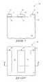
- FIG. 1is a diagrammatic cross section of a substrate fragment at commencement of processing according to an embodiment of the invention, and taken through line 1 - 1 in FIG. 2 .
- FIG. 2is a diagrammatic top plan view of the FIG. 1 substrate fragment.
- FIG. 3is a view of the FIG. 1 substrate fragment at a processing step subsequent to that shown by FIG. 1 , and taken through line 3 - 3 in FIG. 4 .
- FIG. 4is diagrammatic top plan view of the FIG. 3 substrate fragment.
- FIG. 5is a view of the FIG. 3 substrate fragment at a processing step subsequent to that shown by FIG. 3 .
- FIG. 6is a view of the FIG. 5 substrate fragment at a processing step subsequent to that shown by FIG. 5 .
- FIG. 7is a view of the FIG. 6 substrate fragment at a processing step subsequent to that shown by FIG. 6 .
- FIG. 8is a view of the FIG. 7 substrate fragment at a processing step subsequent to that shown by FIG. 7 .
- FIG. 9is a view of the FIG. 8 substrate fragment at a processing step subsequent to that shown by FIG. 8 .
- FIG. 10is a view of the FIG. 9 substrate fragment at a processing step subsequent to that shown by FIG. 9 , and taken through line 10 - 10 in FIG. 11 .
- FIG. 11is a diagrammatic top plan view of the FIG. 10 substrate fragment.
- FIG. 12is a view of the FIG. 10 substrate fragment at a processing step subsequent to that shown by FIG. 10 .
- FIG. 13is a view of the FIG. 12 substrate fragment at a processing step subsequent to that shown by FIG. 12 .
- FIG. 14is a view of the FIG. 13 substrate fragment at a processing step subsequent to that shown by FIG. 13 .
- FIG. 15is a view of the FIG. 14 substrate fragment at a processing step subsequent to that shown by FIG. 14 , and taken through line 15 - 15 in FIG. 16 .
- FIG. 16is a diagrammatic top plan view of the FIG. 15 substrate fragment.
- FIG. 17is a view of the FIG. 15 substrate fragment at a processing step subsequent to that shown by FIG. 15 , and taken through line 17 - 17 in FIG. 18 .
- FIG. 18is a diagrammatic top plan view of the FIG. 17 substrate fragment.
- FIG. 19is a diagrammatic cross section of another embodiment substrate fragment.
- FIG. 20is a view of the FIG. 19 substrate fragment at a processing step subsequent to that shown by FIG. 19 .
- FIG. 21is a diagrammatic cross section of yet another embodiment substrate fragment.
- FIG. 22is a view of the FIG. 21 substrate fragment at a processing step subsequent to that shown by FIG. 21 .
- FIG. 23is a view of the FIG. 22 substrate fragment at a processing step subsequent to that shown by FIG. 22 .
- FIG. 24is a schematic representation of DRAM circuitry.
- a semiconductor substrateis indicated generally with reference numeral 10 .
- semiconductor substrateor “semiconductive substrate” is defined to mean any construction comprising semiconductor material, including, but not limited to, bulk semiconductor materials such as a semiconductive wafer (either alone or in assemblies comprising other materials thereon), and semiconductor material layers (either alone or in assemblies comprising other materials).
- substraterefers to any supporting structure, including, but not limited to, the semiconductive substrates described above.
- Substrate 10is depicted as comprising bulk semiconductor substrate material 12 , for example monocrystalline silicon.
- Substrate 12may, of course, comprise a different substrate, for example including semiconductor-on-insulator substrates and other substrates whether existing or yet-to-be developed.
- a field trench isolation mask 15has been formed and patterned over substrate material 12 .
- suchcomprises a pad oxide layer 14 having a silicon nitride-comprising layer 13 formed thereover.
- Much of the material beneath layers 14 and 13 of field trench isolation mask 15will constitute active area, while much of the exposed region of mask 15 will constitute trench isolation.
- a pair of trenches 16has been etched within semiconductor substrate 10 into semiconductor material 12 .
- An example etch depth for trenches 16is from 800 to 1,000 Angstroms.
- semiconductor material 12may be considered as comprising a semiconductor material channel region 18 comprising opposing sides 20 and 22 extending along a length “L” of the channel region 18 . Accordingly, trenches 16 are formed on opposing sides 20 , 22 of semiconductor material channel region 18 along channel length L.
- Substrate 10would typically, of course, comprise more masked regions 15 , and a series of such trenches 16 would likely be etched over substrate 10 .
- An example dry anisotropic etching chemistry to produce the FIGS. 3 and 4 constructionincludes a combination of HBr and Cl 2 .
- trenches 16have been lined with one or more suitable masking materials 24 , and which has been subsequently anisotropically etched to expose a semiconductor material base 26 of substrate material 12 .
- An example material 24is silicon nitride formed by chemical vapor deposition and/or by plasma or other nitridation of semiconductor material 12 .
- An example lateral thickness of material 24is from 60 Angstroms to 90 Angstroms. Accordingly, such provide but one example manner by which trenches 16 can be formed to have lined sidewalls and an exposed semiconductor material base 26 .
- bulbous lower portions 27comprise projections 28 , 29 extending laterally outward relative to the lined trench sidewalls referred to above.
- One projection of each bulbous lower portion 27opposes and extends towards a projection of the other bulbous lower portion, with the projections that have been designated with numeral 28 being shown as constituting such example opposing projections.
- bulbous lower portions 27may be considered as comprising respective floors 30 .
- an example isotropic etching chemistry to produce the depicted bulbous lower portionsincludes a dry etching chemistry using HBr and NF 3 .
- An example added depth to trenches 16 beyond the depth shown by the FIG. 3 etchis from 800 to 1,000 Angstroms.
- substantially anisotropic etchinghas been conducted through floors 30 of bulbous lower portions 27 to extend pair of trenches 16 deeper within semiconductor substrate 10 .
- An example added depth for the depicted lower stem portions of such trenchesis from 500 to 1,000 Angstroms.
- the etch chemistry and parametersare switched back to anisotropic in situ.
- trenches 16have been lined with one or more suitable materials 32 , for example one or more layers of silicon dioxide and/or silicon nitride. Such might be deposited by one or both of chemical vapor deposition and/or thermal/plasma nitridation and/or oxidation of the sidewalls of the depicted trenches.
- An example thickness for layer 32is from 50 to 150 Angstroms.
- one or more insulative materials 34have been deposited effective to fill remaining volume of trenches 16 with insulative material.
- Material 34is also depicted as being planarized back at least to the outer portion of silicon nitride layer 13 .
- trench isolation masking layer 13may be removed from the substrate prior to deposition of insulative material 34 .
- an example material 34is high plasma density deposited silicon dioxide.
- trench isolation material 34can be considered as comprising opposing insulative projections 36 which extend toward one another along channel length L, and insulative projections 38 .
- semiconductor material 12 of substrate 10is received over/atop insulative projections 36 , as shown.
- insulative projections 36are received partially under channel region 18 , as shown.
- trench isolation masking material 13may be removed from the substrate prior to or after the formation of trench isolation material 34 .
- substrate 10 at this pointwill be patterned for ultimate desired formation of fin channel features while protecting the cell contact, bit contact, and field trench isolation regions of the structure. Such might be accomplished in any number of manners, with FIGS. 10 and 11 illustrating but one embodiment of such masking and patterning.
- FIGS. 10 and 11depict materials 13 and 14 having been removed, and insulative material 34 having been etched back.
- One or more masking materials 40have been deposited and patterned primarily for the fabrication of fin-channel regions. Material 40 patterned over channel regions 18 will not necessarily be patterned to conform to the outline of channel regions 18 (as shown).
- Suchmay be patterned to essentially cover all (not shown) of the semiconductor material between trench isolation material 34 / 32 in the FIG. 10 cross-section.
- all of such semiconductor material in the FIG. 10 cross-section between trench isolation material 34may be outwardly exposed, and thereby not masked by material 40 .
- An example preferred material 40is silicon nitride deposited to an example thickness range of from 600 to 1,200 Angstroms.
- trench isolation material 34has been etched to expose opposing sides 41 of semiconductor material 12 along channel length L. Such etching might be isotropic, anisotropic, or a combination of one or more of anisotropic and isotropic etching steps.
- trench isolation material 34comprises high density plasma deposited silicon dioxide
- an example anisotropic dry etching chemistrycomprises a combination of C 4 F 6 , C 4 F 8 , O 2 , He, and Ar
- an example isotropic wet etching chemistrycomprises a buffered aqueous HF solution.
- a lining 24remains from the example preferred FIG. 5 processing, and where such comprises silicon nitride, such is also etched (as shown) and an example silicon nitride etching chemistry to expose semiconductor material sidewalls 41 comprises a combination of CH 2 F 2 and O 2 .
- FIG. 12illustrates the etching of trench isolation material 34 being conducted at least elevationally to opposing insulative projections 36 , which is preferred.
- FIG. 13illustrates an example of continuing the FIG. 12 etching in a dry, substantially anisotropic manner into trench isolation material 34 which is laterally adjacent the trench insulative material 34 / 32 of opposing insulative projections 36 .
- such etching of trench isolation material 34 / 32is depicted as not being into any insulative material 34 / 32 within the opposing insulative projections 36 , although other embodiments are of course contemplated, for example as will be described below. Further in one embodiment and as depicted in FIG.
- opposing insulative projections 36can be considered as having some elevational thickness “T” having an elevational mid-point “M”, and having floors “F”.
- Etching of trench isolation material 34has been at least to mid-point M of elevational thickness T, and is precisely thereat. The etching of trench isolation 34 and 32 , however, is desirably not conducted all the way to floors F.
- semiconductor material 12 along channel length Lcan be considered as having a top 46 , with such top 46 being masked during etching of the exposed opposing sides of semiconductor material 12 to form channel fin 45 , and with such masking occurring by way of example only from material 40 .
- example top 46is unmasked during the semiconductor material etching to form channel fin 45 .
- etching of semiconductor material 12 to form projecting channel fin 45may desirably be conducted in a substantially anisotropic manner, with an example of an etching chemistry to produce to the FIG. 14 construction comprising starting with a combination of CF 4 and He, and finishing with HBr.
- Outlines 48are shown that comprise transistor source/drain regions that have or will be fabricated and that connect with a fin channel region 45 .
- a gate 52has been formed over a top and opposing sides 20 , 22 of fin channel region 45 along channel length L. Such is depicted as being formed by forming a gate dielectric layer 54 , followed by the deposition of one or more conductive layers 56 (including one or more conductively doped semiconductor layers), and patterning of at least conductive material 56 into line-shaped configurations 52 , for example as shown in FIG. 18 . Source/drain doping and/or construction may be subsequently finalized, or may have been essentially completed previously to form source/drains 48 . For example, FIG. 18 depicts two transistors 51 and 53 having been fabricated, and which by way of example share a source/drain region 48 between the depicted gate lines 52 .
- FIGS. 19 and 20Another embodiment is shown in FIGS. 19 and 20 with respect to a substrate fragment 10 a .
- Like numerals from the first-described embodimenthave been utilized where appropriate, with differences being indicated with the suffix “a”.
- FIG. 19is analogous to the FIG. 13 substrate depiction; however, where masking material 40 of FIG. 13 has been removed from/is not provided over what will be the fin channel region. Further, a greater quantity of semiconductor material 12 has been provided above opposing insulative projections 36 .
- exposed opposing sides of semiconductor material 12have been etched along channel length L to form an upwardly projecting channel fin 45 a .
- the top of material 12 along channel length Lis unmasked during the etching of the exposed opposing sides of semiconductor material 12 to form the channel fin, and the etching of such top desirably occurs during the etching of the exposed opposing sides to form the channel fin.
- a combination of isotropic and anisotropic etchesmight be conducted in lieu of the foregoing.
- gates(not shown) may be fabricated subsequently, analogous to that shown in FIGS. 17 and 18 .
- FIGS. 21-23Another embodiment is shown in FIGS. 21-23 with respect to a substrate fragment 10 b .
- Like numerals from the first-described embodimenthave been utilized where appropriate, with differences being indicated with the suffix “b”.
- FIG. 21essentially depicts processing subsequent to or continuing of that shown by the first embodiment substrate of FIG. 12 .
- FIG. 13depicted the etching of trench isolation material 34 in a manner which was not into any insulative material within opposing insulative projections 36 . Etching however may also, of course, occur into insulative projections 36 in connection with the above-identified substrates 10 and 10 a embodiments.
- FIG. 21essentially depicts processing subsequent to or continuing of that shown by the first embodiment substrate of FIG. 12 .
- FIG. 13depicted the etching of trench isolation material 34 in a manner which was not into any insulative material within opposing insulative projections 36 . Etching however may also, of course, occur into insulative projections 36 in connection with the above
- FIG. 21depicts an embodiment wherein at least some of trench isolation material 34 / 32 is etched from opposing insulative projections 36 to form projections 36 b and 38 b .
- FIG. 21illustrates substantially isotropic etching of trench isolation material 34 / 32 and within projections 36 to elevational mid-point M.
- An example isotropic etching chemistry to remove material 34includes an aqueous buffered HF solution.
- An isotropic etching chemistry to remove material 24 and 32includes a combination of CH 2 F 2 and O 2 .
- FIG. 22depicts subsequent etching of the exposed opposing sides of semiconductor material 12 along channel length L to form an upwardly projecting channel fin 45 b .
- FIG. 23depicts subsequent processing for the fabrication of a gate 52 b , including conductive material 56 b and gate dielectric 54 b.
- the above substrates 10 and 10 aprovide embodiments whereby insulative material 34 / 32 within each of opposing projections 36 is at least partially received under upwardly projecting fin 45 .
- the substrates 10 and 10 a embodimentsdepict substrates having insulative projection inner surfaces 95 ( FIGS. 17 and 20 ) extending along the length of the channel which are convexly curved relative to the fin thickness transverse the channel length.
- the FIG. 22 embodimentdepicts one example field effect transistor wherein none of insulative material 34 / 32 within each of opposing projections 36 b in the finished construction is received under upwardly projecting channel fin 45 b.
- etching of some of the trench isolation materialoccurs from opposing insulative projections prior to etching the exposed opposing sides of the semiconductor material to form the channel fin.
- Embodiments of the inventionalso contemplate conducting at least some of the etching of the trench isolation material from the opposing insulative projection commensurate with the etching of the exposed opposing sides of the semiconductor material to form the channel fin.
- a single substantially anisotropic etching chemistrymay be utilized to directly go from the FIG. 10 depiction to produce the FIG. 22 construction.
- Some embodiments of the inventionencompass methods of forming one or more field effect transistors by the above-described methods. Some embodiments of the invention also contemplate a plurality of field effect transistors independent of the method of fabrication. By way of example only, one embodiment contemplates a plurality of field effect transistors wherein individual of such transistors comprise a semiconductor substrate comprising a pair of source/drain regions having a fin channel region received therebetween.
- the fin channel regioncomprises a channel length extending between the pair of source/drain regions, opposing channel sides extending along the length of the channel region, and a top extending along the length of the channel region.
- the fin channel regionhas a maximum thickness transverse the channel length.
- a gateis received over the fin channel top and the channel sides along the channel length.
- Insulative materialis received immediately beneath the fin channel region extending along the channel length, and extends only partially across the fin channel maximum thickness transverse the channel length.
- the insulative materialincludes opposing portions projecting inwardly toward one another under the fin channel region relative to the fin channel maximum thickness along the channel length.
- An embodiment of the inventionencompasses a plurality of field effect transistors wherein individual of such transistors comprise a bulk semiconductor substrate comprising a pair of source/drain regions having a fin channel region received therebetween.
- the fin channel regioncomprises a channel length extending between the pair of source/drain regions, opposing channel sides extending along the length of the channel region, and a top extending along the length of the channel region.
- a gateis received over the fin channel top and the channel sides along the channel length.
- Trench isolationis received within the bulk semiconductor substrate elevationally lower than the fin channel region and extends along the opposing channel sides along the channel length.
- the trench isolation in cross-section transverse the channel lengthcomprises a lower trench stem and upper transverse projections extending from the stem transversely towards and elevationally lower than the fin channel.
- Embodiments of the inventionalso encompass DRAM circuitry comprising a plurality of individual memory cells.
- Individual of the memory cellscomprise a field effect transistor having a pair of source/drain regions, a capacitor connected with one of the source/drain regions, and a bit line contact connected with another of the source/drain regions.
- FIG. 24depicts an example such DRAM memory cell 75 encompassing a transistor 53 (i.e., transistor 53 of FIG. 18 ).
- a capacitor 70is connected with one of source/drain regions 48 and a bit line contact 80 connected with another of source/drain regions 48 .
- bit line contact 80would connect with source/drain region 48 shown in FIG. 18 between the depicted gate lines 52 of transistor 73 with a bit line, and the lower-depicted source/drain region 48 of transistor 53 in FIG. 18 would connect with an appropriate capacitor 70 .
Landscapes
- Engineering & Computer Science (AREA)
- Manufacturing & Machinery (AREA)
- Physics & Mathematics (AREA)
- Condensed Matter Physics & Semiconductors (AREA)
- General Physics & Mathematics (AREA)
- Computer Hardware Design (AREA)
- Microelectronics & Electronic Packaging (AREA)
- Power Engineering (AREA)
- Insulated Gate Type Field-Effect Transistor (AREA)
- Semiconductor Memories (AREA)
Abstract
Description
- Embodiments disclosed herein pertain to methods of forming field effect transistors, to pluralities of field effect transistors, and to DRAM circuitry comprising a plurality of individual memory cells.
- Field effect transistors are devices commonly used in the fabrication of integrated circuitry. Such devices conventionally comprise a pair of conductive source/drain regions having a semiconductive channel region therebetween. A conductive gate is received operably proximate the channel region, and is separated therefrom by a dielectric material. Application of suitable voltage to the gate causes current to flow from one of the source/drain regions to the other through the channel region, accordingly operating as a switch depending upon voltage application to the gate.
- Integrated circuitry fabrication technology continues to strive to make smaller and denser circuits, with the corresponding size of individual devices, of course, shrinking in the process. As the size of field effect transistors gets smaller and the length of the channels between the source/drain regions shortens, complex channel profiles have been developed to achieve desired “on” threshold voltages and to alleviate undesired short channel effects. Such profiles for the channel regions can include gating the channel region from multiple sides. One example such device is a FinFET. Such structures are built on semiconductor-on-insulator substrates in which the semiconductor material (typically silicon) is etched into a “fin”-like shaped channel body of the transistor, with the conductive gate wrapping up and over the “fin”.
- “Fin”-shaped channel body regions have also been proposed in bulk semiconductor processing in addition to semiconductor-on-insulator processing. Etching of the semiconductor material to produce the typical vertically-extending channel fins can create shoulder areas of semiconductor material adjacent the base of the fins. Such areas can result in undesired parasitic capacitance as the conductive gate is also typically received over these shoulder semiconductor material areas.
FIG. 1 is a diagrammatic cross section of a substrate fragment at commencement of processing according to an embodiment of the invention, and taken through line1-1 inFIG. 2 .FIG. 2 is a diagrammatic top plan view of theFIG. 1 substrate fragment.FIG. 3 is a view of theFIG. 1 substrate fragment at a processing step subsequent to that shown byFIG. 1 , and taken through line3-3 inFIG. 4 .FIG. 4 is diagrammatic top plan view of theFIG. 3 substrate fragment.FIG. 5 is a view of theFIG. 3 substrate fragment at a processing step subsequent to that shown byFIG. 3 .FIG. 6 is a view of theFIG. 5 substrate fragment at a processing step subsequent to that shown byFIG. 5 .FIG. 7 is a view of theFIG. 6 substrate fragment at a processing step subsequent to that shown byFIG. 6 .FIG. 8 is a view of theFIG. 7 substrate fragment at a processing step subsequent to that shown byFIG. 7 .FIG. 9 is a view of theFIG. 8 substrate fragment at a processing step subsequent to that shown byFIG. 8 .FIG. 10 is a view of theFIG. 9 substrate fragment at a processing step subsequent to that shown byFIG. 9 , and taken through line10-10 inFIG. 11 .FIG. 11 is a diagrammatic top plan view of theFIG. 10 substrate fragment.FIG. 12 is a view of theFIG. 10 substrate fragment at a processing step subsequent to that shown byFIG. 10 .FIG. 13 is a view of theFIG. 12 substrate fragment at a processing step subsequent to that shown byFIG. 12 .FIG. 14 is a view of theFIG. 13 substrate fragment at a processing step subsequent to that shown byFIG. 13 .FIG. 15 is a view of theFIG. 14 substrate fragment at a processing step subsequent to that shown byFIG. 14 , and taken through line15-15 inFIG. 16 .FIG. 16 is a diagrammatic top plan view of theFIG. 15 substrate fragment.FIG. 17 is a view of theFIG. 15 substrate fragment at a processing step subsequent to that shown byFIG. 15 , and taken through line17-17 inFIG. 18 .FIG. 18 is a diagrammatic top plan view of theFIG. 17 substrate fragment.FIG. 19 is a diagrammatic cross section of another embodiment substrate fragment.FIG. 20 is a view of theFIG. 19 substrate fragment at a processing step subsequent to that shown byFIG. 19 .FIG. 21 is a diagrammatic cross section of yet another embodiment substrate fragment.FIG. 22 is a view of theFIG. 21 substrate fragment at a processing step subsequent to that shown byFIG. 21 .FIG. 23 is a view of theFIG. 22 substrate fragment at a processing step subsequent to that shown byFIG. 22 .FIG. 24 is a schematic representation of DRAM circuitry.- Example embodiments of the invention are described in connection with
FIGS. 1-24 . Referring initially toFIGS. 1 and 2 , a semiconductor substrate is indicated generally withreference numeral 10. In the context of this document, the term “semiconductor substrate” or “semiconductive substrate” is defined to mean any construction comprising semiconductor material, including, but not limited to, bulk semiconductor materials such as a semiconductive wafer (either alone or in assemblies comprising other materials thereon), and semiconductor material layers (either alone or in assemblies comprising other materials). The term “substrate” refers to any supporting structure, including, but not limited to, the semiconductive substrates described above.Substrate 10 is depicted as comprising bulksemiconductor substrate material 12, for example monocrystalline silicon.Substrate 12 may, of course, comprise a different substrate, for example including semiconductor-on-insulator substrates and other substrates whether existing or yet-to-be developed. - A field
trench isolation mask 15 has been formed and patterned oversubstrate material 12. In the depicted embodiment, such comprises apad oxide layer 14 having a silicon nitride-comprisinglayer 13 formed thereover. Much of the material beneathlayers trench isolation mask 15 will constitute active area, while much of the exposed region ofmask 15 will constitute trench isolation. - Referring to
FIGS. 3 and 4 , a pair oftrenches 16 has been etched withinsemiconductor substrate 10 intosemiconductor material 12. An example etch depth fortrenches 16 is from 800 to 1,000 Angstroms. For purposes of the continuing discussion,semiconductor material 12 may be considered as comprising a semiconductormaterial channel region 18 comprisingopposing sides channel region 18. Accordingly,trenches 16 are formed onopposing sides material channel region 18 along channellength L. Substrate 10 would typically, of course, comprise moremasked regions 15, and a series ofsuch trenches 16 would likely be etched oversubstrate 10. An example dry anisotropic etching chemistry to produce theFIGS. 3 and 4 construction includes a combination of HBr and Cl2. - Referring to
FIG. 5 ,trenches 16 have been lined with one or moresuitable masking materials 24, and which has been subsequently anisotropically etched to expose asemiconductor material base 26 ofsubstrate material 12. Anexample material 24 is silicon nitride formed by chemical vapor deposition and/or by plasma or other nitridation ofsemiconductor material 12. An example lateral thickness ofmaterial 24 is from 60 Angstroms to 90 Angstroms. Accordingly, such provide but one example manner by whichtrenches 16 can be formed to have lined sidewalls and an exposedsemiconductor material base 26. - Referring to
FIG. 6 , semiconductor material bases26 (not shown) have been substantially isotropically etched through effective to form a bulbouslower portion 27 of eachtrench 16. Each of bulbouslower portions 27 comprisesprojections lower portion 27 opposes and extends towards a projection of the other bulbous lower portion, with the projections that have been designated withnumeral 28 being shown as constituting such example opposing projections. For purposes of the continuing discussion, bulbouslower portions 27 may be considered as comprisingrespective floors 30. Wheresemiconductor material 12 comprises monocrystalline silicon, an example isotropic etching chemistry to produce the depicted bulbous lower portions includes a dry etching chemistry using HBr and NF3. An example added depth to trenches16 beyond the depth shown by theFIG. 3 etch is from 800 to 1,000 Angstroms. - Referring to
FIG. 7 , substantially anisotropic etching has been conducted throughfloors 30 of bulbouslower portions 27 to extend pair oftrenches 16 deeper withinsemiconductor substrate 10. An example added depth for the depicted lower stem portions of such trenches is from 500 to 1,000 Angstroms. Most desirably, the etch chemistry and parameters are switched back to anisotropic in situ. - Referring to
FIG. 8 ,trenches 16 have been lined with one or moresuitable materials 32, for example one or more layers of silicon dioxide and/or silicon nitride. Such might be deposited by one or both of chemical vapor deposition and/or thermal/plasma nitridation and/or oxidation of the sidewalls of the depicted trenches. An example thickness forlayer 32 is from 50 to 150 Angstroms. - Referring to
FIG. 9 , one or moreinsulative materials 34 have been deposited effective to fill remaining volume oftrenches 16 with insulative material.Material 34 is also depicted as being planarized back at least to the outer portion ofsilicon nitride layer 13. Alternatively and by way of example only, trench isolation masking layer13 (and also perhaps layer14) may be removed from the substrate prior to deposition ofinsulative material 34. Regardless, anexample material 34 is high plasma density deposited silicon dioxide. - Such provides but one example method of forming
trench isolation material 34 within asemiconductor substrate 12 and on opposingsides material channel region 18 along a length L of the channel region.Trench isolation material 34/32 can be considered as comprising opposinginsulative projections 36 which extend toward one another along channel length L, andinsulative projections 38. In one embodiment,semiconductor material 12 ofsubstrate 10 is received over/atopinsulative projections 36, as shown. In one embodiment,insulative projections 36 are received partially underchannel region 18, as shown. - As referred to above, trench
isolation masking material 13 may be removed from the substrate prior to or after the formation oftrench isolation material 34. Regardless, preferablysubstrate 10 at this point will be patterned for ultimate desired formation of fin channel features while protecting the cell contact, bit contact, and field trench isolation regions of the structure. Such might be accomplished in any number of manners, withFIGS. 10 and 11 illustrating but one embodiment of such masking and patterning.FIGS. 10 and 11 depictmaterials insulative material 34 having been etched back. One ormore masking materials 40 have been deposited and patterned primarily for the fabrication of fin-channel regions.Material 40 patterned overchannel regions 18 will not necessarily be patterned to conform to the outline of channel regions18 (as shown). Further, such may be patterned to essentially cover all (not shown) of the semiconductor material betweentrench isolation material 34/32 in theFIG. 10 cross-section. Alternatively and by way of example only, and as will be subsequently described in connection with another embodiment, all of such semiconductor material in theFIG. 10 cross-section betweentrench isolation material 34 may be outwardly exposed, and thereby not masked bymaterial 40. An example preferredmaterial 40 is silicon nitride deposited to an example thickness range of from 600 to 1,200 Angstroms. - Referring to
FIG. 12 ,trench isolation material 34 has been etched to expose opposingsides 41 ofsemiconductor material 12 along channel length L. Such etching might be isotropic, anisotropic, or a combination of one or more of anisotropic and isotropic etching steps. Wheretrench isolation material 34 comprises high density plasma deposited silicon dioxide, an example anisotropic dry etching chemistry comprises a combination of C4F6, C4F8, O2, He, and Ar, whereas an example isotropic wet etching chemistry comprises a buffered aqueous HF solution. Where a lining24 remains from the example preferredFIG. 5 processing, and where such comprises silicon nitride, such is also etched (as shown) and an example silicon nitride etching chemistry to exposesemiconductor material sidewalls 41 comprises a combination of CH2F2and O2. FIG. 12 illustrates the etching oftrench isolation material 34 being conducted at least elevationally to opposinginsulative projections 36, which is preferred.FIG. 13 illustrates an example of continuing theFIG. 12 etching in a dry, substantially anisotropic manner intotrench isolation material 34 which is laterally adjacent thetrench insulative material 34/32 of opposinginsulative projections 36. In one embodiment and as shown, such etching oftrench isolation material 34/32 is depicted as not being into anyinsulative material 34/32 within the opposinginsulative projections 36, although other embodiments are of course contemplated, for example as will be described below. Further in one embodiment and as depicted inFIG. 13 , opposinginsulative projections 36 can be considered as having some elevational thickness “T” having an elevational mid-point “M”, and having floors “F”. Etching oftrench isolation material 34, as shown inFIG. 13 , has been at least to mid-point M of elevational thickness T, and is precisely thereat. The etching oftrench isolation - Referring to
FIG. 14 , exposed opposing sides41 (not shown due to their removal) ofsemiconductor material 12 have been etched along channel length L to form achannel fin 45. In the depicted exampleFIG. 14 embodiment, such is projecting upwardly, preferably relative to opposinginsulative projections 36. For purposes of the continuing discussion,semiconductor material 12 along channel length L can be considered as having a top46, with such top46 being masked during etching of the exposed opposing sides ofsemiconductor material 12 to formchannel fin 45, and with such masking occurring by way of example only frommaterial 40. Another embodiment is described below wherebyexample top 46 is unmasked during the semiconductor material etching to formchannel fin 45. Regardless, etching ofsemiconductor material 12 to form projectingchannel fin 45 may desirably be conducted in a substantially anisotropic manner, with an example of an etching chemistry to produce to theFIG. 14 construction comprising starting with a combination of CF4and He, and finishing with HBr. - Referring to
FIGS. 15 and 16 , an example of subsequent processing is shown whereby maskingmaterial 40 has been removed.Outlines 48 are shown that comprise transistor source/drain regions that have or will be fabricated and that connect with afin channel region 45. - Referring to
FIGS. 17 and 18 , agate 52 has been formed over a top and opposingsides fin channel region 45 along channel length L. Such is depicted as being formed by forming agate dielectric layer 54, followed by the deposition of one or more conductive layers56 (including one or more conductively doped semiconductor layers), and patterning of at leastconductive material 56 into line-shapedconfigurations 52, for example as shown inFIG. 18 . Source/drain doping and/or construction may be subsequently finalized, or may have been essentially completed previously to form source/drains48. For example,FIG. 18 depicts twotransistors drain region 48 between the depicted gate lines52. - The above-described embodiment masked the top of the semiconductor material along the channel length during etching of the exposed opposing sides of the semiconductor material to form the channel fin. By way of example only, another embodiment is shown in
FIGS. 19 and 20 with respect to asubstrate fragment 10a. Like numerals from the first-described embodiment have been utilized where appropriate, with differences being indicated with the suffix “a”.FIG. 19 is analogous to theFIG. 13 substrate depiction; however, where maskingmaterial 40 ofFIG. 13 has been removed from/is not provided over what will be the fin channel region. Further, a greater quantity ofsemiconductor material 12 has been provided above opposinginsulative projections 36. - Referring to
FIG. 20 , exposed opposing sides ofsemiconductor material 12 have been etched along channel length L to form an upwardly projectingchannel fin 45a. Accordingly in the depictedFIGS. 19 and 20 example, the top ofmaterial 12 along channel length L is unmasked during the etching of the exposed opposing sides ofsemiconductor material 12 to form the channel fin, and the etching of such top desirably occurs during the etching of the exposed opposing sides to form the channel fin. A combination of isotropic and anisotropic etches might be conducted in lieu of the foregoing. Regardless, gates (not shown) may be fabricated subsequently, analogous to that shown inFIGS. 17 and 18 . - Another embodiment is shown in
FIGS. 21-23 with respect to asubstrate fragment 10b. Like numerals from the first-described embodiment have been utilized where appropriate, with differences being indicated with the suffix “b”.FIG. 21 essentially depicts processing subsequent to or continuing of that shown by the first embodiment substrate ofFIG. 12 .FIG. 13 depicted the etching oftrench isolation material 34 in a manner which was not into any insulative material within opposinginsulative projections 36. Etching however may also, of course, occur intoinsulative projections 36 in connection with the above-identifiedsubstrates FIG. 21 depicts an embodiment wherein at least some oftrench isolation material 34/32 is etched from opposinginsulative projections 36 to formprojections FIG. 21 illustrates substantially isotropic etching oftrench isolation material 34/32 and withinprojections 36 to elevational mid-point M. An example isotropic etching chemistry to removematerial 34 includes an aqueous buffered HF solution. An isotropic etching chemistry to removematerial FIG. 22 depicts subsequent etching of the exposed opposing sides ofsemiconductor material 12 along channel length L to form an upwardly projectingchannel fin 45b.FIG. 23 depicts subsequent processing for the fabrication of agate 52b, includingconductive material 56band gate dielectric54b.- The
above substrates insulative material 34/32 within each of opposingprojections 36 is at least partially received under upwardly projectingfin 45. Further, thesubstrates FIGS. 17 and 20 ) extending along the length of the channel which are convexly curved relative to the fin thickness transverse the channel length. TheFIG. 22 embodiment depicts one example field effect transistor wherein none ofinsulative material 34/32 within each of opposingprojections 36bin the finished construction is received under upwardly projectingchannel fin 45b. - The above-described processing is particularly desirable wherein the etching of some of the trench isolation material occurs from opposing insulative projections prior to etching the exposed opposing sides of the semiconductor material to form the channel fin. Embodiments of the invention also contemplate conducting at least some of the etching of the trench isolation material from the opposing insulative projection commensurate with the etching of the exposed opposing sides of the semiconductor material to form the channel fin. By way of example only, a single substantially anisotropic etching chemistry may be utilized to directly go from the
FIG. 10 depiction to produce theFIG. 22 construction. - Some embodiments of the invention, of course, encompass methods of forming one or more field effect transistors by the above-described methods. Some embodiments of the invention also contemplate a plurality of field effect transistors independent of the method of fabrication. By way of example only, one embodiment contemplates a plurality of field effect transistors wherein individual of such transistors comprise a semiconductor substrate comprising a pair of source/drain regions having a fin channel region received therebetween. The fin channel region comprises a channel length extending between the pair of source/drain regions, opposing channel sides extending along the length of the channel region, and a top extending along the length of the channel region. The fin channel region has a maximum thickness transverse the channel length.
- A gate is received over the fin channel top and the channel sides along the channel length. Insulative material is received immediately beneath the fin channel region extending along the channel length, and extends only partially across the fin channel maximum thickness transverse the channel length. The insulative material includes opposing portions projecting inwardly toward one another under the fin channel region relative to the fin channel maximum thickness along the channel length. By way of example only, an individual of such field effect transistors is shown with respect to the embodiments exemplified by
FIGS. 17 ,18 and20 above. Desirable sizes and materials of construction and configurations may otherwise be as described above. - An embodiment of the invention encompasses a plurality of field effect transistors wherein individual of such transistors comprise a bulk semiconductor substrate comprising a pair of source/drain regions having a fin channel region received therebetween. The fin channel region comprises a channel length extending between the pair of source/drain regions, opposing channel sides extending along the length of the channel region, and a top extending along the length of the channel region.
- A gate is received over the fin channel top and the channel sides along the channel length. Trench isolation is received within the bulk semiconductor substrate elevationally lower than the fin channel region and extends along the opposing channel sides along the channel length. The trench isolation in cross-section transverse the channel length comprises a lower trench stem and upper transverse projections extending from the stem transversely towards and elevationally lower than the fin channel. Each of the above embodiments depict such an example individual field effect transistor channel region, wherein the lower portion of the trench etched below the bulbous portion can be considered as a lower trench stem having upper transverse projections encompassed by
projections 36/36b. - Embodiments of the invention also encompass DRAM circuitry comprising a plurality of individual memory cells. Individual of the memory cells comprise a field effect transistor having a pair of source/drain regions, a capacitor connected with one of the source/drain regions, and a bit line contact connected with another of the source/drain regions. For example,
FIG. 24 depicts an example suchDRAM memory cell 75 encompassing a transistor53 (i.e.,transistor 53 ofFIG. 18 ). Acapacitor 70 is connected with one of source/drain regions 48 and a bit line contact80 connected with another of source/drain regions 48. For example, bit line contact80 would connect with source/drain region 48 shown inFIG. 18 between the depictedgate lines 52 of transistor73 with a bit line, and the lower-depicted source/drain region 48 oftransistor 53 inFIG. 18 would connect with anappropriate capacitor 70. - In compliance with the statute, the invention has been described in language more or less specific as to structural and methodical features. It is to be understood, however, that the invention is not limited to the specific features shown and described, since the means herein disclosed comprise preferred forms of putting the invention into effect. The invention is, therefore, claimed in any of its forms or modifications within the proper scope of the appended claims appropriately interpreted in accordance with the doctrine of equivalents.
Claims (26)
Priority Applications (2)
| Application Number | Priority Date | Filing Date | Title |
|---|---|---|---|
| US13/070,256US8222102B2 (en) | 2006-11-17 | 2011-03-23 | Methods of forming field effect transistors, pluralities of field effect transistors, and DRAM circuitry comprising a plurality of individual memory cells |
| US13/528,028US8409946B2 (en) | 2006-11-17 | 2012-06-20 | Methods of forming field effect transistors, pluralities of field effect transistors, and DRAM circuitry comprising a plurality of individual memory cells |
Applications Claiming Priority (2)
| Application Number | Priority Date | Filing Date | Title |
|---|---|---|---|
| US11/601,478US7939403B2 (en) | 2006-11-17 | 2006-11-17 | Methods of forming a field effect transistors, pluralities of field effect transistors, and DRAM circuitry comprising a plurality of individual memory cells |
| US13/070,256US8222102B2 (en) | 2006-11-17 | 2011-03-23 | Methods of forming field effect transistors, pluralities of field effect transistors, and DRAM circuitry comprising a plurality of individual memory cells |
Related Parent Applications (1)
| Application Number | Title | Priority Date | Filing Date |
|---|---|---|---|
| US11/601,478ContinuationUS7939403B2 (en) | 2006-11-17 | 2006-11-17 | Methods of forming a field effect transistors, pluralities of field effect transistors, and DRAM circuitry comprising a plurality of individual memory cells |
Related Child Applications (1)
| Application Number | Title | Priority Date | Filing Date |
|---|---|---|---|
| US13/528,028ContinuationUS8409946B2 (en) | 2006-11-17 | 2012-06-20 | Methods of forming field effect transistors, pluralities of field effect transistors, and DRAM circuitry comprising a plurality of individual memory cells |
Publications (2)
| Publication Number | Publication Date |
|---|---|
| US20110169086A1true US20110169086A1 (en) | 2011-07-14 |
| US8222102B2 US8222102B2 (en) | 2012-07-17 |
Family
ID=39135289
Family Applications (3)
| Application Number | Title | Priority Date | Filing Date |
|---|---|---|---|
| US11/601,478Active2029-07-25US7939403B2 (en) | 2006-11-17 | 2006-11-17 | Methods of forming a field effect transistors, pluralities of field effect transistors, and DRAM circuitry comprising a plurality of individual memory cells |
| US13/070,256ActiveUS8222102B2 (en) | 2006-11-17 | 2011-03-23 | Methods of forming field effect transistors, pluralities of field effect transistors, and DRAM circuitry comprising a plurality of individual memory cells |
| US13/528,028ActiveUS8409946B2 (en) | 2006-11-17 | 2012-06-20 | Methods of forming field effect transistors, pluralities of field effect transistors, and DRAM circuitry comprising a plurality of individual memory cells |
Family Applications Before (1)
| Application Number | Title | Priority Date | Filing Date |
|---|---|---|---|
| US11/601,478Active2029-07-25US7939403B2 (en) | 2006-11-17 | 2006-11-17 | Methods of forming a field effect transistors, pluralities of field effect transistors, and DRAM circuitry comprising a plurality of individual memory cells |
Family Applications After (1)
| Application Number | Title | Priority Date | Filing Date |
|---|---|---|---|
| US13/528,028ActiveUS8409946B2 (en) | 2006-11-17 | 2012-06-20 | Methods of forming field effect transistors, pluralities of field effect transistors, and DRAM circuitry comprising a plurality of individual memory cells |
Country Status (5)
| Country | Link |
|---|---|
| US (3) | US7939403B2 (en) |
| KR (1) | KR101093931B1 (en) |
| CN (1) | CN101536166B (en) |
| SG (1) | SG176485A1 (en) |
| WO (1) | WO2008063357A1 (en) |
Cited By (2)
| Publication number | Priority date | Publication date | Assignee | Title |
|---|---|---|---|---|
| CN106098743A (en)* | 2015-04-29 | 2016-11-09 | 台湾积体电路制造股份有限公司 | The high aspect ratio etch that top does not broadens |
| US10269637B2 (en)* | 2016-12-02 | 2019-04-23 | Taiwan Semiconductor Manufacturing Co., Ltd. | Semiconductor structure and fabricating method thereof |
Families Citing this family (31)
| Publication number | Priority date | Publication date | Assignee | Title |
|---|---|---|---|---|
| WO2005036721A2 (en) | 2003-10-06 | 2005-04-21 | Edward Woods | Power generation systems and methods of generating power |
| US7422960B2 (en) | 2006-05-17 | 2008-09-09 | Micron Technology, Inc. | Method of forming gate arrays on a partial SOI substrate |
| US7537994B2 (en) | 2006-08-28 | 2009-05-26 | Micron Technology, Inc. | Methods of forming semiconductor devices, assemblies and constructions |
| US7939403B2 (en) | 2006-11-17 | 2011-05-10 | Micron Technology, Inc. | Methods of forming a field effect transistors, pluralities of field effect transistors, and DRAM circuitry comprising a plurality of individual memory cells |
| US8110890B2 (en)* | 2007-06-05 | 2012-02-07 | Taiwan Semiconductor Manufacturing Company, Ltd. | Method of fabricating semiconductor device isolation structure |
| US7816216B2 (en)* | 2007-07-09 | 2010-10-19 | Micron Technology, Inc. | Semiconductor device comprising transistor structures and methods for forming same |
| US7879659B2 (en)* | 2007-07-17 | 2011-02-01 | Micron Technology, Inc. | Methods of fabricating semiconductor devices including dual fin structures |
| JP2010003916A (en)* | 2008-06-20 | 2010-01-07 | Elpida Memory Inc | Semiconductor device and method of manufacturing the same |
| US9202921B2 (en)* | 2010-03-30 | 2015-12-01 | Nanya Technology Corp. | Semiconductor device and method of making the same |
| US8624300B2 (en) | 2010-12-16 | 2014-01-07 | Intel Corporation | Contact integration for three-dimensional stacking semiconductor devices |
| US20130043559A1 (en)* | 2011-08-17 | 2013-02-21 | International Business Machines Corporation | Trench formation in substrate |
| CN103035709B (en)* | 2011-09-30 | 2015-11-25 | 中国科学院微电子研究所 | Semiconductor structure and manufacturing method thereof |
| US20130093062A1 (en)* | 2011-10-18 | 2013-04-18 | Ying-Chih Lin | Semiconductor structure and process thereof |
| TWI587382B (en)* | 2011-10-19 | 2017-06-11 | 聯華電子股份有限公司 | Semiconductor structure and process thereof |
| KR101908980B1 (en) | 2012-04-23 | 2018-10-17 | 삼성전자주식회사 | Field effect transistor |
| KR101976846B1 (en)* | 2012-08-16 | 2019-05-09 | 에스케이하이닉스 주식회사 | Semiconductor memory device and manufacturing method thereof |
| US9257559B2 (en)* | 2014-01-15 | 2016-02-09 | Taiwan Semiconductor Manufacturing Company Limited | Semiconductor device and formation thereof |
| US9263455B2 (en) | 2013-07-23 | 2016-02-16 | Micron Technology, Inc. | Methods of forming an array of conductive lines and methods of forming an array of recessed access gate lines |
| US9219116B2 (en) | 2014-01-15 | 2015-12-22 | Taiwan Semiconductor Manufacturing Company, Ltd. | Fin structure of semiconductor device |
| US10468528B2 (en) | 2014-04-16 | 2019-11-05 | Taiwan Semiconductor Manufacturing Company, Ltd. | FinFET device with high-k metal gate stack |
| US9721955B2 (en) | 2014-04-25 | 2017-08-01 | Taiwan Semiconductor Manufacturing Company, Ltd. | Structure and method for SRAM FinFET device having an oxide feature |
| US9178067B1 (en) | 2014-04-25 | 2015-11-03 | Taiwan Semiconductor Manufacturing Company, Ltd. | Structure and method for FinFET device |
| US9224736B1 (en) | 2014-06-27 | 2015-12-29 | Taiwan Semicondcutor Manufacturing Company, Ltd. | Structure and method for SRAM FinFET device |
| KR102481427B1 (en)* | 2016-01-13 | 2022-12-27 | 삼성전자주식회사 | Semiconductor device and method for manufacturing the same |
| US9793271B1 (en)* | 2016-04-29 | 2017-10-17 | International Business Machines Corporation | Semiconductor device with different fin pitches |
| US9773893B1 (en) | 2016-09-26 | 2017-09-26 | International Business Machines Corporation | Forming a sacrificial liner for dual channel devices |
| US10388763B2 (en)* | 2016-12-15 | 2019-08-20 | Taiwan Semiconductor Manufacturing Co., Ltd. | Manufacturing of semiconductor fin structure and manufacturing method of semiconductor device |
| KR102420163B1 (en)* | 2018-01-18 | 2022-07-12 | 삼성전자주식회사 | Integrated circuit device and method of manufacturing the same |
| CN111799329B (en) | 2019-04-08 | 2024-11-29 | 三星电子株式会社 | Semiconductor device with a semiconductor layer having a plurality of semiconductor layers |
| CN112038340B (en)* | 2019-06-04 | 2024-08-23 | 长鑫存储技术有限公司 | Memory structure and forming method thereof |
| US20240282860A1 (en)* | 2023-02-20 | 2024-08-22 | International Business Machines Corporation | Nonlinear channel |
Citations (20)
| Publication number | Priority date | Publication date | Assignee | Title |
|---|---|---|---|---|
| US5466621A (en)* | 1988-11-21 | 1995-11-14 | Hitachi, Ltd. | Method of manufacturing a semiconductor device having silicon islands |
| US5612230A (en)* | 1991-04-16 | 1997-03-18 | Canon Kabushiki Kaisha | Process for manufacturing a semiconductor device by applying a non-single-crystalline material on a sidewall inside of an opening portion for growing a single-crystalline semiconductor body |
| US5801083A (en)* | 1997-10-20 | 1998-09-01 | Chartered Semiconductor Manufacturing, Ltd. | Use of polymer spacers for the fabrication of shallow trench isolation regions with rounded top corners |
| US6285057B1 (en)* | 1999-11-17 | 2001-09-04 | National Semiconductor Corporation | Semiconductor device combining a MOSFET structure and a vertical-channel trench-substrate field effect device |
| US6300215B1 (en)* | 1998-10-19 | 2001-10-09 | Samsung Electronics Co., Ltd. | Methods of forming integrated circuit capacitors having composite titanium oxide and tantalum pentoxide dielectric layers therein |
| US6642090B1 (en)* | 2002-06-03 | 2003-11-04 | International Business Machines Corporation | Fin FET devices from bulk semiconductor and method for forming |
| US20040110358A1 (en)* | 2002-12-09 | 2004-06-10 | Lee Joon Hyeon | Method for forming isolation film for semiconductor devices |
| US20040110383A1 (en)* | 2002-12-05 | 2004-06-10 | Hiroyuki Tanaka | Method of forming device isolation trench |
| US20040150071A1 (en)* | 2002-12-27 | 2004-08-05 | Masaki Kondo | Double-gate structure fin-type transistor |
| US20040195610A1 (en)* | 2003-03-17 | 2004-10-07 | Mutsuo Morikado | Fin semiconductor device and method for fabricating the same |
| US20040262687A1 (en)* | 2003-06-27 | 2004-12-30 | In-Soo Jung | Fin field effect transistors and fabrication methods thereof |
| US20050136617A1 (en)* | 2003-12-03 | 2005-06-23 | Young-Chul Jang | MOS transistor having protruded-shape channel and method of fabricating the same |
| US20050199932A1 (en)* | 2004-03-11 | 2005-09-15 | Abbott Todd R. | Semiconductor constructions, and methods of forming semiconductor structures |
| US20050250279A1 (en)* | 2004-03-05 | 2005-11-10 | Yong-Hoon Son | Methods of forming semiconductor devices having buried oxide patterns and devices related thereto |
| US20060046428A1 (en)* | 2004-08-30 | 2006-03-02 | International Business Machines Corporation | Trench sidewall passivation for lateral rie in a selective silicon-on-insulator process flow |
| US20060076595A1 (en)* | 2004-09-25 | 2006-04-13 | Hsiao-Che Wu | Dynamic random access memory cell and fabricating method thereof |
| US7407847B2 (en)* | 2006-03-31 | 2008-08-05 | Intel Corporation | Stacked multi-gate transistor design and method of fabrication |
| US7413955B2 (en)* | 2005-06-01 | 2008-08-19 | Hynix Semiconductor Inc. | Transistor for memory device and method for manufacturing the same |
| US7422960B2 (en)* | 2006-05-17 | 2008-09-09 | Micron Technology, Inc. | Method of forming gate arrays on a partial SOI substrate |
| US7935602B2 (en)* | 2005-06-28 | 2011-05-03 | Micron Technology, Inc. | Semiconductor processing methods |
Family Cites Families (6)
| Publication number | Priority date | Publication date | Assignee | Title |
|---|---|---|---|---|
| US6313008B1 (en) | 2001-01-25 | 2001-11-06 | Chartered Semiconductor Manufacturing Inc. | Method to form a balloon shaped STI using a micro machining technique to remove heavily doped silicon |
| DE10157785A1 (en) | 2001-11-27 | 2003-06-12 | Austriamicrocsystems Ag Schlos | Isolation trench for an integrated circuit and method for its production |
| KR100530496B1 (en)* | 2004-04-20 | 2005-11-22 | 삼성전자주식회사 | Semiconductor device, method of forming a recess gate electrode and method of manufacturing a semiconductor device having the same |
| JP4409348B2 (en)* | 2004-04-26 | 2010-02-03 | 三菱電機株式会社 | Semiconductor device and manufacturing method thereof |
| KR100660881B1 (en)* | 2005-10-12 | 2006-12-26 | 삼성전자주식회사 | Semiconductor device with vertical channel transistor and manufacturing method thereof |
| US7939403B2 (en)* | 2006-11-17 | 2011-05-10 | Micron Technology, Inc. | Methods of forming a field effect transistors, pluralities of field effect transistors, and DRAM circuitry comprising a plurality of individual memory cells |
- 2006
- 2006-11-17USUS11/601,478patent/US7939403B2/enactiveActive
- 2007
- 2007-10-29CNCN2007800420203Apatent/CN101536166B/enactiveActive
- 2007-10-29SGSG2011084449Apatent/SG176485A1/enunknown
- 2007-10-29WOPCT/US2007/022856patent/WO2008063357A1/enactiveApplication Filing
- 2007-10-29KRKR1020097010166Apatent/KR101093931B1/enactiveActive
- 2011
- 2011-03-23USUS13/070,256patent/US8222102B2/enactiveActive
- 2012
- 2012-06-20USUS13/528,028patent/US8409946B2/enactiveActive
Patent Citations (20)
| Publication number | Priority date | Publication date | Assignee | Title |
|---|---|---|---|---|
| US5466621A (en)* | 1988-11-21 | 1995-11-14 | Hitachi, Ltd. | Method of manufacturing a semiconductor device having silicon islands |
| US5612230A (en)* | 1991-04-16 | 1997-03-18 | Canon Kabushiki Kaisha | Process for manufacturing a semiconductor device by applying a non-single-crystalline material on a sidewall inside of an opening portion for growing a single-crystalline semiconductor body |
| US5801083A (en)* | 1997-10-20 | 1998-09-01 | Chartered Semiconductor Manufacturing, Ltd. | Use of polymer spacers for the fabrication of shallow trench isolation regions with rounded top corners |
| US6300215B1 (en)* | 1998-10-19 | 2001-10-09 | Samsung Electronics Co., Ltd. | Methods of forming integrated circuit capacitors having composite titanium oxide and tantalum pentoxide dielectric layers therein |
| US6285057B1 (en)* | 1999-11-17 | 2001-09-04 | National Semiconductor Corporation | Semiconductor device combining a MOSFET structure and a vertical-channel trench-substrate field effect device |
| US6642090B1 (en)* | 2002-06-03 | 2003-11-04 | International Business Machines Corporation | Fin FET devices from bulk semiconductor and method for forming |
| US20040110383A1 (en)* | 2002-12-05 | 2004-06-10 | Hiroyuki Tanaka | Method of forming device isolation trench |
| US20040110358A1 (en)* | 2002-12-09 | 2004-06-10 | Lee Joon Hyeon | Method for forming isolation film for semiconductor devices |
| US20040150071A1 (en)* | 2002-12-27 | 2004-08-05 | Masaki Kondo | Double-gate structure fin-type transistor |
| US20040195610A1 (en)* | 2003-03-17 | 2004-10-07 | Mutsuo Morikado | Fin semiconductor device and method for fabricating the same |
| US20040262687A1 (en)* | 2003-06-27 | 2004-12-30 | In-Soo Jung | Fin field effect transistors and fabrication methods thereof |
| US20050136617A1 (en)* | 2003-12-03 | 2005-06-23 | Young-Chul Jang | MOS transistor having protruded-shape channel and method of fabricating the same |
| US20050250279A1 (en)* | 2004-03-05 | 2005-11-10 | Yong-Hoon Son | Methods of forming semiconductor devices having buried oxide patterns and devices related thereto |
| US20050199932A1 (en)* | 2004-03-11 | 2005-09-15 | Abbott Todd R. | Semiconductor constructions, and methods of forming semiconductor structures |
| US20060046428A1 (en)* | 2004-08-30 | 2006-03-02 | International Business Machines Corporation | Trench sidewall passivation for lateral rie in a selective silicon-on-insulator process flow |
| US20060076595A1 (en)* | 2004-09-25 | 2006-04-13 | Hsiao-Che Wu | Dynamic random access memory cell and fabricating method thereof |
| US7413955B2 (en)* | 2005-06-01 | 2008-08-19 | Hynix Semiconductor Inc. | Transistor for memory device and method for manufacturing the same |
| US7935602B2 (en)* | 2005-06-28 | 2011-05-03 | Micron Technology, Inc. | Semiconductor processing methods |
| US7407847B2 (en)* | 2006-03-31 | 2008-08-05 | Intel Corporation | Stacked multi-gate transistor design and method of fabrication |
| US7422960B2 (en)* | 2006-05-17 | 2008-09-09 | Micron Technology, Inc. | Method of forming gate arrays on a partial SOI substrate |
Cited By (2)
| Publication number | Priority date | Publication date | Assignee | Title |
|---|---|---|---|---|
| CN106098743A (en)* | 2015-04-29 | 2016-11-09 | 台湾积体电路制造股份有限公司 | The high aspect ratio etch that top does not broadens |
| US10269637B2 (en)* | 2016-12-02 | 2019-04-23 | Taiwan Semiconductor Manufacturing Co., Ltd. | Semiconductor structure and fabricating method thereof |
Also Published As
| Publication number | Publication date |
|---|---|
| US8222102B2 (en) | 2012-07-17 |
| SG176485A1 (en) | 2011-12-29 |
| US8409946B2 (en) | 2013-04-02 |
| US7939403B2 (en) | 2011-05-10 |
| US20120256244A1 (en) | 2012-10-11 |
| WO2008063357A1 (en) | 2008-05-29 |
| KR20090080984A (en) | 2009-07-27 |
| CN101536166A (en) | 2009-09-16 |
| US20080119020A1 (en) | 2008-05-22 |
| KR101093931B1 (en) | 2011-12-13 |
| CN101536166B (en) | 2012-06-27 |
Similar Documents
| Publication | Publication Date | Title |
|---|---|---|
| US7939403B2 (en) | Methods of forming a field effect transistors, pluralities of field effect transistors, and DRAM circuitry comprising a plurality of individual memory cells | |
| KR100584776B1 (en) | Active structure formation method, device isolation method and transistor formation method of semiconductor device | |
| US9231051B2 (en) | Methods of forming spacers on FinFETs and other semiconductor devices | |
| US7935600B2 (en) | Method of manufacturing multi-channel transistor device and multi-channel transistor device manufactured using the method | |
| US20080166856A1 (en) | Methods of Forming Recessed Access Devices Associated With Semiconductor Constructions | |
| US7358144B2 (en) | Method for fabricating semiconductor device | |
| US20060105529A1 (en) | Methods of forming MOS transistors having buried gate electrodes therein | |
| KR20070094616A (en) | Semiconductor manufacturing process including source / drain regions recessed in SiO wafer | |
| US7563683B2 (en) | Transistor and method of fabricating the same | |
| KR100487657B1 (en) | mos transistor with recessed gate and method of fabricating the same | |
| KR100702302B1 (en) | Manufacturing Method of Semiconductor Device | |
| US7674677B2 (en) | Semiconductor device and a method for manufacturing the same | |
| KR100701701B1 (en) | Semiconductor device and manufacturing method thereof | |
| KR100319642B1 (en) | Transistor forming method | |
| KR101052871B1 (en) | Semiconductor device and manufacturing method thereof | |
| KR100629694B1 (en) | Semiconductor device manufacturing method | |
| KR100657824B1 (en) | Fin transistor and its manufacturing method | |
| KR100568754B1 (en) | Transistors and manufacturing methods thereof | |
| KR101046380B1 (en) | Semiconductor device and manufacturing method thereof | |
| KR20050118548A (en) | Method for manufacturing self-aligned recess channel mosfet |
Legal Events
| Date | Code | Title | Description |
|---|---|---|---|
| FEPP | Fee payment procedure | Free format text:PAYOR NUMBER ASSIGNED (ORIGINAL EVENT CODE: ASPN); ENTITY STATUS OF PATENT OWNER: LARGE ENTITY | |
| STCF | Information on status: patent grant | Free format text:PATENTED CASE | |
| FPAY | Fee payment | Year of fee payment:4 | |
| AS | Assignment | Owner name:U.S. BANK NATIONAL ASSOCIATION, AS COLLATERAL AGENT, CALIFORNIA Free format text:SECURITY INTEREST;ASSIGNOR:MICRON TECHNOLOGY, INC.;REEL/FRAME:038669/0001 Effective date:20160426 Owner name:U.S. BANK NATIONAL ASSOCIATION, AS COLLATERAL AGEN Free format text:SECURITY INTEREST;ASSIGNOR:MICRON TECHNOLOGY, INC.;REEL/FRAME:038669/0001 Effective date:20160426 | |
| AS | Assignment | Owner name:MORGAN STANLEY SENIOR FUNDING, INC., AS COLLATERAL AGENT, MARYLAND Free format text:PATENT SECURITY AGREEMENT;ASSIGNOR:MICRON TECHNOLOGY, INC.;REEL/FRAME:038954/0001 Effective date:20160426 Owner name:MORGAN STANLEY SENIOR FUNDING, INC., AS COLLATERAL Free format text:PATENT SECURITY AGREEMENT;ASSIGNOR:MICRON TECHNOLOGY, INC.;REEL/FRAME:038954/0001 Effective date:20160426 | |
| AS | Assignment | Owner name:U.S. BANK NATIONAL ASSOCIATION, AS COLLATERAL AGENT, CALIFORNIA Free format text:CORRECTIVE ASSIGNMENT TO CORRECT THE REPLACE ERRONEOUSLY FILED PATENT #7358718 WITH THE CORRECT PATENT #7358178 PREVIOUSLY RECORDED ON REEL 038669 FRAME 0001. ASSIGNOR(S) HEREBY CONFIRMS THE SECURITY INTEREST;ASSIGNOR:MICRON TECHNOLOGY, INC.;REEL/FRAME:043079/0001 Effective date:20160426 Owner name:U.S. BANK NATIONAL ASSOCIATION, AS COLLATERAL AGEN Free format text:CORRECTIVE ASSIGNMENT TO CORRECT THE REPLACE ERRONEOUSLY FILED PATENT #7358718 WITH THE CORRECT PATENT #7358178 PREVIOUSLY RECORDED ON REEL 038669 FRAME 0001. ASSIGNOR(S) HEREBY CONFIRMS THE SECURITY INTEREST;ASSIGNOR:MICRON TECHNOLOGY, INC.;REEL/FRAME:043079/0001 Effective date:20160426 | |
| AS | Assignment | Owner name:JPMORGAN CHASE BANK, N.A., AS COLLATERAL AGENT, ILLINOIS Free format text:SECURITY INTEREST;ASSIGNORS:MICRON TECHNOLOGY, INC.;MICRON SEMICONDUCTOR PRODUCTS, INC.;REEL/FRAME:047540/0001 Effective date:20180703 Owner name:JPMORGAN CHASE BANK, N.A., AS COLLATERAL AGENT, IL Free format text:SECURITY INTEREST;ASSIGNORS:MICRON TECHNOLOGY, INC.;MICRON SEMICONDUCTOR PRODUCTS, INC.;REEL/FRAME:047540/0001 Effective date:20180703 | |
| AS | Assignment | Owner name:MICRON TECHNOLOGY, INC., IDAHO Free format text:RELEASE BY SECURED PARTY;ASSIGNOR:U.S. BANK NATIONAL ASSOCIATION, AS COLLATERAL AGENT;REEL/FRAME:047243/0001 Effective date:20180629 | |
| AS | Assignment | Owner name:MICRON TECHNOLOGY, INC., IDAHO Free format text:RELEASE BY SECURED PARTY;ASSIGNOR:MORGAN STANLEY SENIOR FUNDING, INC., AS COLLATERAL AGENT;REEL/FRAME:050937/0001 Effective date:20190731 | |
| AS | Assignment | Owner name:MICRON TECHNOLOGY, INC., IDAHO Free format text:RELEASE BY SECURED PARTY;ASSIGNOR:JPMORGAN CHASE BANK, N.A., AS COLLATERAL AGENT;REEL/FRAME:051028/0001 Effective date:20190731 Owner name:MICRON SEMICONDUCTOR PRODUCTS, INC., IDAHO Free format text:RELEASE BY SECURED PARTY;ASSIGNOR:JPMORGAN CHASE BANK, N.A., AS COLLATERAL AGENT;REEL/FRAME:051028/0001 Effective date:20190731 | |
| MAFP | Maintenance fee payment | Free format text:PAYMENT OF MAINTENANCE FEE, 8TH YEAR, LARGE ENTITY (ORIGINAL EVENT CODE: M1552); ENTITY STATUS OF PATENT OWNER: LARGE ENTITY Year of fee payment:8 | |
| MAFP | Maintenance fee payment | Free format text:PAYMENT OF MAINTENANCE FEE, 12TH YEAR, LARGE ENTITY (ORIGINAL EVENT CODE: M1553); ENTITY STATUS OF PATENT OWNER: LARGE ENTITY Year of fee payment:12 |