US20110169082A1 - Method for forming retrograded well for mosfet - Google Patents
Method for forming retrograded well for mosfetDownload PDFInfo
- Publication number
- US20110169082A1 US20110169082A1US12/687,287US68728710AUS2011169082A1US 20110169082 A1US20110169082 A1US 20110169082A1US 68728710 AUS68728710 AUS 68728710AUS 2011169082 A1US2011169082 A1US 2011169082A1
- Authority
- US
- United States
- Prior art keywords
- semiconductor layer
- semiconductor
- layer
- dielectric layer
- retrograded well
- Prior art date
- Legal status (The legal status is an assumption and is not a legal conclusion. Google has not performed a legal analysis and makes no representation as to the accuracy of the status listed.)
- Granted
Links
- 238000000034methodMethods0.000titleclaimsabstractdescription98
- 239000004065semiconductorSubstances0.000claimsabstractdescription292
- 239000002019doping agentSubstances0.000claimsabstractdescription66
- 239000000758substrateSubstances0.000claimsabstractdescription55
- 239000000463materialSubstances0.000claimsdescription72
- 238000005468ion implantationMethods0.000claimsdescription31
- 239000007943implantSubstances0.000claimsdescription20
- 238000000151depositionMethods0.000claimsdescription16
- XUIMIQQOPSSXEZ-UHFFFAOYSA-NSiliconChemical compound[Si]XUIMIQQOPSSXEZ-UHFFFAOYSA-N0.000claimsdescription13
- 150000004767nitridesChemical class0.000claimsdescription13
- 229910052710siliconInorganic materials0.000claimsdescription13
- 239000010703siliconSubstances0.000claimsdescription13
- 125000006850spacer groupChemical group0.000claimsdescription11
- 238000005530etchingMethods0.000claimsdescription8
- 229910000577Silicon-germaniumInorganic materials0.000claimsdescription7
- 239000012212insulatorSubstances0.000claimsdescription6
- 230000003213activating effectEffects0.000claimsdescription5
- 230000008021depositionEffects0.000claimsdescription5
- 238000005224laser annealingMethods0.000claimsdescription5
- 239000004020conductorSubstances0.000claims4
- 238000005229chemical vapour depositionMethods0.000description28
- 239000003989dielectric materialSubstances0.000description27
- 230000005669field effectEffects0.000description16
- 238000005240physical vapour depositionMethods0.000description10
- 238000002955isolationMethods0.000description8
- 229920002120photoresistant polymerPolymers0.000description8
- 238000000623plasma-assisted chemical vapour depositionMethods0.000description8
- 229910021420polycrystalline siliconInorganic materials0.000description8
- 229910052785arsenicInorganic materials0.000description7
- 229910052751metalInorganic materials0.000description7
- 239000002184metalSubstances0.000description7
- ZOXJGFHDIHLPTG-UHFFFAOYSA-NBoronChemical compound[B]ZOXJGFHDIHLPTG-UHFFFAOYSA-N0.000description5
- VYPSYNLAJGMNEJ-UHFFFAOYSA-NSilicium dioxideChemical compoundO=[Si]=OVYPSYNLAJGMNEJ-UHFFFAOYSA-N0.000description5
- RQNWIZPPADIBDY-UHFFFAOYSA-Narsenic atomChemical compound[As]RQNWIZPPADIBDY-UHFFFAOYSA-N0.000description5
- 229910052796boronInorganic materials0.000description5
- 229910044991metal oxideInorganic materials0.000description5
- 150000004706metal oxidesChemical class0.000description5
- 229920005591polysiliconPolymers0.000description5
- 229910052814silicon oxideInorganic materials0.000description5
- JBRZTFJDHDCESZ-UHFFFAOYSA-NAsGaChemical compound[As]#[Ga]JBRZTFJDHDCESZ-UHFFFAOYSA-N0.000description4
- 229910001218Gallium arsenideInorganic materials0.000description4
- 229910052581Si3N4Inorganic materials0.000description4
- 239000000956alloySubstances0.000description4
- 238000001505atmospheric-pressure chemical vapour depositionMethods0.000description4
- 238000006243chemical reactionMethods0.000description4
- 150000001875compoundsChemical class0.000description4
- 230000000694effectsEffects0.000description4
- 239000012535impuritySubstances0.000description4
- RPQDHPTXJYYUPQ-UHFFFAOYSA-Nindium arsenideChemical compound[In]#[As]RPQDHPTXJYYUPQ-UHFFFAOYSA-N0.000description4
- 150000002500ionsChemical class0.000description4
- 238000004518low pressure chemical vapour depositionMethods0.000description4
- 229910052698phosphorusInorganic materials0.000description4
- 238000001020plasma etchingMethods0.000description4
- 229910021332silicideInorganic materials0.000description4
- HQVNEWCFYHHQES-UHFFFAOYSA-Nsilicon nitrideChemical compoundN12[Si]34N5[Si]62N3[Si]51N64HQVNEWCFYHHQES-UHFFFAOYSA-N0.000description4
- 239000000126substanceSubstances0.000description4
- 229910000927Ge alloyInorganic materials0.000description3
- 229910000673Indium arsenideInorganic materials0.000description3
- GPXJNWSHGFTCBW-UHFFFAOYSA-NIndium phosphideChemical compound[In]#PGPXJNWSHGFTCBW-UHFFFAOYSA-N0.000description3
- LEVVHYCKPQWKOP-UHFFFAOYSA-N[Si].[Ge]Chemical compound[Si].[Ge]LEVVHYCKPQWKOP-UHFFFAOYSA-N0.000description3
- 229910045601alloyInorganic materials0.000description3
- 238000000231atomic layer depositionMethods0.000description3
- 230000015572biosynthetic processEffects0.000description3
- 239000000969carrierSubstances0.000description3
- 230000000295complement effectEffects0.000description3
- 238000005137deposition processMethods0.000description3
- -1hafnium silicatesChemical class0.000description3
- 238000004519manufacturing processMethods0.000description3
- 230000003647oxidationEffects0.000description3
- 238000007254oxidation reactionMethods0.000description3
- 238000000206photolithographyMethods0.000description3
- 229910010271silicon carbideInorganic materials0.000description3
- HBMJWWWQQXIZIP-UHFFFAOYSA-Nsilicon carbideChemical compound[Si+]#[C-]HBMJWWWQQXIZIP-UHFFFAOYSA-N0.000description3
- OAICVXFJPJFONN-UHFFFAOYSA-NPhosphorusChemical compound[P]OAICVXFJPJFONN-UHFFFAOYSA-N0.000description2
- 229910003811SiGeCInorganic materials0.000description2
- 239000000853adhesiveSubstances0.000description2
- 230000001070adhesive effectEffects0.000description2
- 229910052787antimonyInorganic materials0.000description2
- 238000002513implantationMethods0.000description2
- 230000010354integrationEffects0.000description2
- MRELNEQAGSRDBK-UHFFFAOYSA-Nlanthanum oxideInorganic materials[O-2].[O-2].[O-2].[La+3].[La+3]MRELNEQAGSRDBK-UHFFFAOYSA-N0.000description2
- 239000000203mixtureSubstances0.000description2
- 229910003465moissaniteInorganic materials0.000description2
- 239000011574phosphorusSubstances0.000description2
- FVBUAEGBCNSCDD-UHFFFAOYSA-Nsilicide(4-)Chemical compound[Si-4]FVBUAEGBCNSCDD-UHFFFAOYSA-N0.000description2
- 239000012265solid productSubstances0.000description2
- GYHNNYVSQQEPJS-UHFFFAOYSA-NGalliumChemical compound[Ga]GYHNNYVSQQEPJS-UHFFFAOYSA-N0.000description1
- 229910000530Gallium indium arsenideInorganic materials0.000description1
- 238000004026adhesive bondingMethods0.000description1
- 229910052782aluminiumInorganic materials0.000description1
- XAGFODPZIPBFFR-UHFFFAOYSA-NaluminiumChemical compound[Al]XAGFODPZIPBFFR-UHFFFAOYSA-N0.000description1
- 229910021417amorphous siliconInorganic materials0.000description1
- 238000000137annealingMethods0.000description1
- WATWJIUSRGPENY-UHFFFAOYSA-Nantimony atomChemical compound[Sb]WATWJIUSRGPENY-UHFFFAOYSA-N0.000description1
- 239000003990capacitorSubstances0.000description1
- 238000003486chemical etchingMethods0.000description1
- 238000000224chemical solution depositionMethods0.000description1
- 239000011248coating agentSubstances0.000description1
- 238000000576coating methodMethods0.000description1
- 230000007812deficiencyEffects0.000description1
- 238000001704evaporationMethods0.000description1
- 230000008020evaporationEffects0.000description1
- 239000003574free electronSubstances0.000description1
- 229910052733galliumInorganic materials0.000description1
- 229910052732germaniumInorganic materials0.000description1
- GNPVGFCGXDBREM-UHFFFAOYSA-Ngermanium atomChemical compound[Ge]GNPVGFCGXDBREM-UHFFFAOYSA-N0.000description1
- 238000000227grindingMethods0.000description1
- 229910052735hafniumInorganic materials0.000description1
- WIHZLLGSGQNAGK-UHFFFAOYSA-Nhafnium(4+);oxygen(2-)Chemical class[O-2].[O-2].[Hf+4]WIHZLLGSGQNAGK-UHFFFAOYSA-N0.000description1
- BHEPBYXIRTUNPN-UHFFFAOYSA-Nhydridophosphorus(.) (triplet)Chemical compound[PH]BHEPBYXIRTUNPN-UHFFFAOYSA-N0.000description1
- 238000011065in-situ storageMethods0.000description1
- 238000010348incorporationMethods0.000description1
- 229910052738indiumInorganic materials0.000description1
- APFVFJFRJDLVQX-UHFFFAOYSA-Nindium atomChemical compound[In]APFVFJFRJDLVQX-UHFFFAOYSA-N0.000description1
- 238000003475laminationMethods0.000description1
- 238000000608laser ablationMethods0.000description1
- 229910001092metal group alloyInorganic materials0.000description1
- 150000002739metalsChemical class0.000description1
- 229910021421monocrystalline siliconInorganic materials0.000description1
- SOQBVABWOPYFQZ-UHFFFAOYSA-Noxygen(2-);titanium(4+)Chemical class[O-2].[O-2].[Ti+4]SOQBVABWOPYFQZ-UHFFFAOYSA-N0.000description1
- RVTZCBVAJQQJTK-UHFFFAOYSA-Noxygen(2-);zirconium(4+)Chemical class[O-2].[O-2].[Zr+4]RVTZCBVAJQQJTK-UHFFFAOYSA-N0.000description1
- 229920000642polymerPolymers0.000description1
- 230000005855radiationEffects0.000description1
- 238000004151rapid thermal annealingMethods0.000description1
- 239000000376reactantSubstances0.000description1
- 238000005546reactive sputteringMethods0.000description1
- 238000000926separation methodMethods0.000description1
- 229910000679solderInorganic materials0.000description1
- 238000004544sputter depositionMethods0.000description1
- OGIDPMRJRNCKJF-UHFFFAOYSA-Ntitanium oxideInorganic materials[Ti]=OOGIDPMRJRNCKJF-UHFFFAOYSA-N0.000description1
- 229910001928zirconium oxideInorganic materials0.000description1
Images


Classifications
- H—ELECTRICITY
- H01—ELECTRIC ELEMENTS
- H01L—SEMICONDUCTOR DEVICES NOT COVERED BY CLASS H10
- H01L21/00—Processes or apparatus adapted for the manufacture or treatment of semiconductor or solid state devices or of parts thereof
- H01L21/02—Manufacture or treatment of semiconductor devices or of parts thereof
- H01L21/04—Manufacture or treatment of semiconductor devices or of parts thereof the devices having potential barriers, e.g. a PN junction, depletion layer or carrier concentration layer
- H01L21/18—Manufacture or treatment of semiconductor devices or of parts thereof the devices having potential barriers, e.g. a PN junction, depletion layer or carrier concentration layer the devices having semiconductor bodies comprising elements of Group IV of the Periodic Table or AIIIBV compounds with or without impurities, e.g. doping materials
- H01L21/185—Joining of semiconductor bodies for junction formation
- H01L21/187—Joining of semiconductor bodies for junction formation by direct bonding
- H—ELECTRICITY
- H01—ELECTRIC ELEMENTS
- H01L—SEMICONDUCTOR DEVICES NOT COVERED BY CLASS H10
- H01L21/00—Processes or apparatus adapted for the manufacture or treatment of semiconductor or solid state devices or of parts thereof
- H01L21/67—Apparatus specially adapted for handling semiconductor or electric solid state devices during manufacture or treatment thereof; Apparatus specially adapted for handling wafers during manufacture or treatment of semiconductor or electric solid state devices or components ; Apparatus not specifically provided for elsewhere
- H01L21/683—Apparatus specially adapted for handling semiconductor or electric solid state devices during manufacture or treatment thereof; Apparatus specially adapted for handling wafers during manufacture or treatment of semiconductor or electric solid state devices or components ; Apparatus not specifically provided for elsewhere for supporting or gripping
- H01L21/6835—Apparatus specially adapted for handling semiconductor or electric solid state devices during manufacture or treatment thereof; Apparatus specially adapted for handling wafers during manufacture or treatment of semiconductor or electric solid state devices or components ; Apparatus not specifically provided for elsewhere for supporting or gripping using temporarily an auxiliary support
- H—ELECTRICITY
- H10—SEMICONDUCTOR DEVICES; ELECTRIC SOLID-STATE DEVICES NOT OTHERWISE PROVIDED FOR
- H10D—INORGANIC ELECTRIC SEMICONDUCTOR DEVICES
- H10D62/00—Semiconductor bodies, or regions thereof, of devices having potential barriers
- H10D62/10—Shapes, relative sizes or dispositions of the regions of the semiconductor bodies; Shapes of the semiconductor bodies
- H10D62/17—Semiconductor regions connected to electrodes not carrying current to be rectified, amplified or switched, e.g. channel regions
- H10D62/351—Substrate regions of field-effect devices
- H10D62/357—Substrate regions of field-effect devices of FETs
- H10D62/364—Substrate regions of field-effect devices of FETs of IGFETs
- H10D62/371—Inactive supplementary semiconductor regions, e.g. for preventing punch-through, improving capacity effect or leakage current
- H—ELECTRICITY
- H10—SEMICONDUCTOR DEVICES; ELECTRIC SOLID-STATE DEVICES NOT OTHERWISE PROVIDED FOR
- H10D—INORGANIC ELECTRIC SEMICONDUCTOR DEVICES
- H10D86/00—Integrated devices formed in or on insulating or conducting substrates, e.g. formed in silicon-on-insulator [SOI] substrates or on stainless steel or glass substrates
- H10D86/01—Manufacture or treatment
- H—ELECTRICITY
- H01—ELECTRIC ELEMENTS
- H01L—SEMICONDUCTOR DEVICES NOT COVERED BY CLASS H10
- H01L2221/00—Processes or apparatus adapted for the manufacture or treatment of semiconductor or solid state devices or of parts thereof covered by H01L21/00
- H01L2221/67—Apparatus for handling semiconductor or electric solid state devices during manufacture or treatment thereof; Apparatus for handling wafers during manufacture or treatment of semiconductor or electric solid state devices or components; Apparatus not specifically provided for elsewhere
- H01L2221/683—Apparatus for handling semiconductor or electric solid state devices during manufacture or treatment thereof; Apparatus for handling wafers during manufacture or treatment of semiconductor or electric solid state devices or components; Apparatus not specifically provided for elsewhere for supporting or gripping
- H01L2221/68304—Apparatus for handling semiconductor or electric solid state devices during manufacture or treatment thereof; Apparatus for handling wafers during manufacture or treatment of semiconductor or electric solid state devices or components; Apparatus not specifically provided for elsewhere for supporting or gripping using temporarily an auxiliary support
- H01L2221/6835—Apparatus for handling semiconductor or electric solid state devices during manufacture or treatment thereof; Apparatus for handling wafers during manufacture or treatment of semiconductor or electric solid state devices or components; Apparatus not specifically provided for elsewhere for supporting or gripping using temporarily an auxiliary support used as a support during build up manufacturing of active devices
- H—ELECTRICITY
- H01—ELECTRIC ELEMENTS
- H01L—SEMICONDUCTOR DEVICES NOT COVERED BY CLASS H10
- H01L2221/00—Processes or apparatus adapted for the manufacture or treatment of semiconductor or solid state devices or of parts thereof covered by H01L21/00
- H01L2221/67—Apparatus for handling semiconductor or electric solid state devices during manufacture or treatment thereof; Apparatus for handling wafers during manufacture or treatment of semiconductor or electric solid state devices or components; Apparatus not specifically provided for elsewhere
- H01L2221/683—Apparatus for handling semiconductor or electric solid state devices during manufacture or treatment thereof; Apparatus for handling wafers during manufacture or treatment of semiconductor or electric solid state devices or components; Apparatus not specifically provided for elsewhere for supporting or gripping
- H01L2221/68304—Apparatus for handling semiconductor or electric solid state devices during manufacture or treatment thereof; Apparatus for handling wafers during manufacture or treatment of semiconductor or electric solid state devices or components; Apparatus not specifically provided for elsewhere for supporting or gripping using temporarily an auxiliary support
- H01L2221/68368—Apparatus for handling semiconductor or electric solid state devices during manufacture or treatment thereof; Apparatus for handling wafers during manufacture or treatment of semiconductor or electric solid state devices or components; Apparatus not specifically provided for elsewhere for supporting or gripping using temporarily an auxiliary support used in a transfer process involving at least two transfer steps, i.e. including an intermediate handle substrate
Definitions
- first elementsuch as a first structure
- second elementsuch as a second structure
- intervening elementssuch as an interface structure, e.g., interface layer
- the first semiconductor device 100 ais separated from the second semiconductor device 100 b by an isolation region 15 that is formed through the semiconductor layer 14 and contacting the dielectric layer 12 .
- the isolation region 15may comprise any dielectric material, such as oxide, nitride, oxynitride or a combination thereof.
- the isolation region 15comprises a dielectric isolation material selected from the same group of dielectric isolation materials used for the buried dielectric layer 12 .
- a method for fabricating the isolation region 15may be different from a method used for fabricating the buried dielectric layer 12 .
- the source region 22 a and the drain region 22 bmay include raised portions that are formed atop the semiconductor layer 14 .
- the raised portionsmay be composed of epitaxially grown semiconductor material.
- the raised portions of the source region 22 a and the drain region 22 bmay be doped by an in-situ dopant process during epitaxial growth and/or may be doped by ion implantation.
- the source regions 22 a and the drain regions 22 bmay in some embodiments include metal semiconductor alloy contact regions, e.g., silicides, at an upper surface of the source regions 22 a and drain regions 22 b .
- the thermal anneal that activates the dopant of the source regions 22 a and the drain regions 22 breacts a deposited metal on an underlying semiconductor layer to provide the metal semiconductor layer, e.g., silicide.
- the substrate 5is removed by planarization, such as chemical mechanical planarization or grinding, which may be accompanied by separation by ion implantation.
- the substrate 5may be removed by a selective etch process that removes the substrate 5 selective to the dielectric layer 12 .
- the term “selective” in reference to a material removal processdenotes that the rate of material removal for a first material is greater than the rate of removal for at least another material of the structure to which the material removal process is being applied.
- the etch chemistry that removes the substrate 5is selective to the dielectric layer 12 .
- the etch processis an anisotropic etch.
- FIG. 6depicts one embodiment of a semiconductor device having a semiconductor layer 14 overlying a dielectric layer, i.e. buried dielectric layer 60 , in which a gate structure 20 is present on the semiconductor layer 14 .
- Source regions 22 a and drain regions 22 bare typically present within the semiconductor layer 14 adjacent to a portion of the semiconductor layer 14 that the gate structure 20 is in contact with.
- a retrograded well, i.e., activated retrograded well 51may be present between the source regions 22 a and the drain region 22 b , and extending from the dielectric layer, i.e., buried dielectric layer 60 , wherein the activated retrograded well 51 includes dopant of opposite conductivity than the source regions 22 a and the drain regions 22 b .
Landscapes
- Engineering & Computer Science (AREA)
- Physics & Mathematics (AREA)
- Condensed Matter Physics & Semiconductors (AREA)
- General Physics & Mathematics (AREA)
- Manufacturing & Machinery (AREA)
- Computer Hardware Design (AREA)
- Microelectronics & Electronic Packaging (AREA)
- Power Engineering (AREA)
- Metal-Oxide And Bipolar Metal-Oxide Semiconductor Integrated Circuits (AREA)
- Insulated Gate Type Field-Effect Transistor (AREA)
- Thin Film Transistor (AREA)
Abstract
Description
- The present disclosure relates to the fabrication of a semiconductor device, and in one embodiment to a method of fabricating a metal oxide semiconductor field effect transistor (MOSFET) having a retrograded well.
- Over the past twenty-five years or so, the primary challenge of very large scale integration (VLSI) has been the integration of an ever-increasing number of MOSFET devices with high yield and reliability. This was achieved mainly by scaling down MOSFET channel lengths without excessive short-channel effects. Short-channel effects are the decrease in threshold voltage (Vt) in short-channel devices due to two-dimensional electrostatic charge sharing between the gate and the source/drain regions.
- A method of forming a retrograded well is provided, in which in some embodiments the retrograded well is formed after front end of the line processing (FEOL), e.g., after formation of the semiconductor device. In one embodiment, the method includes providing a substrate having a dielectric layer present thereon. A semiconductor layer is present on the dielectric layer. At least one semiconductor device is formed on the semiconductor layer, wherein a gate structure of the at least one semiconductor device is present on a second surface of the semiconductor layer that is opposite a first surface of the semiconductor layer that is in contact with the dielectric layer. Source regions and drain regions are formed in contact with portions of the semiconductor layer that are adjacent to a portion of the semiconductor layer that is in contact with the gate structure. A handling structure is formed on the at least one semiconductor device and the second surface of the semiconductor layer. The substrate and at least a portion of the dielectric layer are removed. A retrograded well is implanted through the first surface of the semiconductor layer. A buried dielectric layer is then formed positioned on the first surface of the semiconductor layer and the handling structure is removed.
- In another embodiment, the method includes providing a semiconductor on insulator (SOI) substrate including a first semiconductor layer and a second semiconductor layer separated by a dielectric layer, and forming at least one semiconductor device on the first semiconductor layer of the SOI substrate. A handling structure is formed contacting the at least one semiconductor device and the first semiconductor layer. The second semiconductor layer and at least a portion of the dielectric layer of the SOI substrate are removed to provide a substantially exposed surface of the first semiconductor layer. A retrograded well may be formed by implanting at least one dopant through the substantially exposed surface of the first semiconductor layer into a first thickness of the semiconductor layer present extending from the substantially exposed surface of the first semiconductor layer. The remaining thickness of the semiconductor layer is substantially free of the at least one dopant of the retrograded well. A buried dielectric layer is then formed on the exposed surface of the semiconductor layer and the handling structure is removed. The retrograded well may be laser annealed.
- In another aspect, a semiconductor device is provided having a retrograded well. In one embodiment, the semiconductor device includes a semiconductor layer overlying a dielectric layer, in which a gate structure is present on the semiconductor layer. Source regions and drain regions are present within the semiconductor layer adjacent to a portion of the semiconductor layer that the gate structure is in contact with. A retrograded well is present between the source regions and the drain regions and extends from the dielectric layer, wherein the retrograded well includes dopant of opposite conductivity than the source and drain regions. The concentration of the dopant of the retrograded well is greater than 1×10¹⁶atoms/cm3. A region substantially free of the dopant of the retrograded well is present extending from the surface of the semiconductor layer that is in contact with the gate structure, and is present over the retrograded well and between the source regions and the drain regions.
- The following detailed description, given by way of example and not intended to limit the invention solely thereto, will best be appreciated in conjunction with the accompanying drawings, wherein like reference numerals denote like elements and parts, in which:
FIG. 1 is a side cross-sectional view depicting providing a substrate having a dielectric layer present thereon, and a semiconductor layer present on the dielectric layer, in accordance with one embodiment of the present method.FIG. 2 is a side cross-sectional view depicting forming at least one semiconductor device on the semiconductor layer, wherein a gate structure of one of the at least one semiconductor device is present on a second surface of the semiconductor layer that is opposite a first surface of the semiconductor layer that is in contact with the dielectric layer, and source regions and drain regions are formed in contact with portions of the semiconductor layer that are adjacent to a portion of the semiconductor layer that is in contact with the gate structure, in accordance with one embodiment of the present method.FIG. 3 is a side cross-sectional view depicting forming at least a portion of a handling structure on the at least one semiconductor device and the second surface of the semiconductor layer, in accordance with one embodiment of the present method.FIG. 4 is a side cross-sectional view depicting removing the substrate and at least a portion of the dielectric layer to substantially expose the first surface of the semiconductor layer, in accordance with one embodiment of the present method.FIG. 5 is a side cross-sectional view depicting forming a retrograded well through the first surface of the semiconductor layer, in accordance with one embodiment of the present method.FIG. 6 is a side cross-sectional view depicting forming a buried dielectric layer on the first surface of the semiconductor layer, removing at least a portion of the handling structure, and activating the retrograded well, in accordance with one embodiment of the present method.- Detailed embodiments of the present invention are disclosed herein; however, it is to be understood that the disclosed embodiments are merely illustrative of the invention that may be embodied in various forms. In addition, each of the examples given in connection with the various embodiments of the invention are intended to be illustrative, and not restrictive. Further, the figures are not necessarily to scale, some features may be exaggerated to show details of particular components. Therefore, specific structural and functional details disclosed herein are not to be interpreted as limiting, but merely as a representative basis for teaching one skilled in the art to variously employ the present invention.
- In some embodiments, methods and structures described herein reduce short channel effects in semiconductor devices, such as metal oxide semiconductor field effect transistors (MOSFETS). In some embodiments, short channel effects are reduced through the incorporation of a retrograded well that is formed through the back side of the semiconductor layer that is housing at least the channel region of a semiconductor device. In one embodiment, the retrograded well is formed after the semiconductor devices have been formed in the semiconductor layer. Therefore, in some examples, the retrograded well may be activated using laser anneal without subjecting the entirety of the semiconductor device to additional thermal anneals. When describing the following structures and methods, the following terms have the following meanings, unless otherwise indicated.
- The term “channel” is the region underlying the gate structure and between the source region and drain region of a semiconductor device that becomes conductive when the semiconductor device is turned on.
- A “retrograded well” is a region that is underlying the channel of the device and has an opposite conductivity type as the source region and the drain region. The retrograded well extends continuously from the source region to the drain region. In the embodiments, in which the channel is present in a semiconductor layer that is present directly on a dielectric layer, i.e., buried dielectric layer of a substrate, the retrograded well is present within a thickness of the semiconductor layer that extends from the surface of the semiconductor layer that contacts the dielectric layer, which is opposite the surface of the semiconductor layer that is in contact with the gate structure.
- As used herein, the term “conductivity type” denotes a dopant region being p-type or n-type.
- The term “direct contact” or “directly on” means that a first element, such as a first structure, and a second element, such as a second structure, are connected without any intermediary conducting, insulating or semiconductor layers at the interface of the two elements.
- The terms “overlying”, “atop”, “positioned on” or “positioned atop” mean that a first element, such as a first structure, is present on a second element, such as a second structure, wherein intervening elements, such as an interface structure, e.g., interface layer, may be present between the first element and the second element.
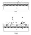
FIGS. 1-6 depict one embodiment of a method for forming an electrical device, in which aretrograded well 50 is formed through the back side of thesemiconductor layer 14 that is housing at least the channel region of thesemiconductor device FIG. 1 depicts one embodiment of providing asubstrate 5 having adielectric layer 12 present thereon.FIG. 1 also shows asemiconductor layer 14 present on thedielectric layer 12. Thesubstrate 5 may comprise any of several semiconductor materials. Non-limiting examples include silicon, germanium, silicon-germanium alloy, silicon carbide, silicon-germanium carbide alloy and compound (i.e., III-V and II-VI) semiconductor materials. Non-limiting examples of compound semiconductor materials include gallium arsenide, indium arsenide and indium phosphide semiconductor materials. Typically, thesubstrate 5 has a thickness ranging from 100 nm to 1.5×10⁶nm.- The
dielectric layer 12 may comprise any of several dielectric materials. Non-limiting examples include oxides, nitrides and oxynitrides, particularly of silicon, but oxides, nitrides and oxynitrides of other elements are not excluded. Thedielectric layer 12 may comprise a crystalline or a non-crystalline dielectric material. Typically, thedielectric layer 12 comprises an oxide of the semiconductor material from which is comprised thesubstrate 5. Typically, thedielectric layer 12 has a thickness ranging from 50 nm to about 2000 nm. - The
dielectric layer 12 may be deposited or formed on a surface of thesubstrate 5, or may be formed within thesubstrate 5. Non-limiting examples include ion implantation methods, thermal or plasma oxidation or nitridation methods, chemical vapor deposition (CVD) methods and physical vapor deposition (PVD) methods. Thedielectric layer 12 may also be formed using a wafer bonding or lamination technique. - In some embodiments, the
dielectric layer 12 includes a layer of a seconddielectric material 13 that is present within thedielectric layer 12. In some examples, the layer of the seconddielectric material 13 is formed by ion implantation. In other examples, the layer of the seconddielectric material 13 is formed by chemical vapor deposition (CVD). For example, a first portion ofdielectric layer 12 may be deposited on thesubstrate 5 using chemical vapor deposition (CVD), e.g., plasma enhanced chemical vapor deposition (PECVD). Thereafter, the layer of a seconddielectric material 13 is may be deposited on the first portion ofdielectric layer 13 using chemical vapor deposition (CVD), e.g., plasma enhanced chemical vapor deposition (PECVD). Thereafter, a second portion ofdielectric layer 12 may be deposited on the layer of a seconddielectric material 13 using chemical vapor deposition (CVD), e.g., plasma enhanced chemical vapor deposition (PECVD). In one embodiment, the layer of the seconddielectric material 13 has a thickness of less than 10 nm, and in some examples ranging from 1 nm to 5 nm. In one example, thedielectric layer 12 is composed of an oxide, such as silicon oxide, and the layer of the seconddielectric material 13 is composed of a nitride, such as silicon nitride. It is noted that the layer of the seconddielectric material 13 is optional, and may be omitted from the present method. - The
semiconductor layer 14 that is present on thedielectric layer 12 may comprise any of the several semiconductor materials from whichsubstrate 5 may also be comprised. Thesemiconductor layer 14 and thesubstrate 5 may comprise either identical or different semiconductor materials with respect to chemical composition, dopant polarity, dopant concentration and crystallographic orientation. In one embodiment, thesemiconductor layer 14 may have a thickness ranging from 2 nm to 100 nm. In another embodiment, thesemiconductor layer 14 has a thickness ranging from 5 nm to 20 nm. In one example, thesemiconductor layer 14 is composed of a silicon-containing material. Illustrative examples of various silicon-containing materials that can be employed in for thesemiconductor layer 14 include, but are not limited to Si, SiGe, SiGeC, SiC and combinations thereof. In another embodiment, thesemiconductor layer 14 may also be Ge, Ge alloys, GaAs, InAs, InP as well as other III/V and II/VI compound semiconductors. Combinations of the aforementioned semiconductor materials can also be used. In one embodiment, thesemiconductor layer 14 is silicon. - In one embodiment, the structure depicted in
FIG. 1 is provided by a semiconductor on insulator (SOI) substrate, in which the semiconductor layer identified byreference number 14 is an SOI layer (also referred to as a first semiconductor layer), the substrate identified byreference number 5 is a base semiconductor layer (also referred to as a second semiconductor layer), and the dielectric layer identified byreference number 12 that is separating the SOI layer from the base semiconductor layer is a buried dielectric layer (also referred to as a buried insulating layer). The components of the SOI substrate may be formed using deposition, thermal growth, ion implantation, or wafer bonding methods. FIG. 2 depicts one embodiment of the formation ofsemiconductor devices semiconductor device semiconductor layer 14. In one embodiment, a semiconductor device is an intrinsic semiconductor material that has been doped, that is, into which a doping agent has been introduced, giving it different electrical properties than the intrinsic semiconductor. Doping involves adding dopant atoms to an intrinsic semiconductor, which changes the electron and hole carrier concentrations of the intrinsic semiconductor at thermal equilibrium. Dominant carrier concentration in an extrinsic semiconductor determines the conductivity type of the semiconductor. In one example, thesemiconductor devices - Although
FIG. 2 only depicts twosemiconductor devices field effect transistor 100a, and a secondfield effect transistor 100b, being formed on thesemiconductor layer 14, it is noted that a greater number or lesser number ofsemiconductor devices semiconductor layer 14 may also include bipolar transistors and may further include memory devices, such as flash memory, dynamic random access memory (DRAM), and embedded dynamic random access memory. It is also noted that the electrical devices incorporated within thesemiconductor layer 14 may also include inductors, capacitors, resistors, fuses and/or diodes. - In one embodiment, a
first semiconductor device 100a, e.g., first field effect transistor, and asecond semiconductor device 100b, e.g., second field effect transistor, may each have the same conductivity. In another embodiment, afirst semiconductor device 100a, e.g., first field effect transistor, and asecond semiconductor device 100b, e.g., second field effect transistor, may have a different conductivity. For example, in the embodiments, in which thefirst semiconductor device 100ahas a different conductivity than thesecond semiconductor device 100b, thefirst semiconductor device 100amay be a p-type field effect transistor, and thesecond semiconductor device 100bmay be an n-type field effect transistor, wherein the first andsecond semiconductor devices - In one embodiment, the
first semiconductor device 100ais separated from thesecond semiconductor device 100bby anisolation region 15 that is formed through thesemiconductor layer 14 and contacting thedielectric layer 12. Theisolation region 15 may comprise any dielectric material, such as oxide, nitride, oxynitride or a combination thereof. Typically, theisolation region 15 comprises a dielectric isolation material selected from the same group of dielectric isolation materials used for the burieddielectric layer 12. However, a method for fabricating theisolation region 15 may be different from a method used for fabricating the burieddielectric layer 12. For example, and without limitation, an isolation dielectric material from which is comprised theisolation region 15 may be deposited using: rapid thermal processing, for example high-temperature oxide also known as HTO, or plasma deposition, for example high-density plasma oxide also known as HDP oxide, or combinations thereof. - Still referring to
FIG. 2 , in one embodiment, agate structure 20 of one of the at least onesemiconductor device semiconductor layer 14 that is opposite afirst surface 51 of thesemiconductor layer 14 that is in contact with thedielectric layer 12. As used herein, “gate structure” means a structure used to control output current (i.e. flow of carriers in the channel) of a semiconducting device through electrical or magnetic fields. Each of the at least onesemiconductor devices source regions 22aanddrain regions 22bthat are formed in contact with portions of thesemiconductor layer 14 that are adjacent to a portion of thesemiconductor layer 14 that is in contact with thegate structure 20. - In one embodiment, the
semiconductor devices gate dielectric 16 located upon the second surface S2 of thesemiconductor layer 14; at least one gate electrode18 located upon the at least onegate dielectric 16; at least onespacer 21 located adjacent opposite sidewalls of the at least onegate dielectric 16 and the at least one gate electrode18 (although intended as completely encircling those structures in plan view); and a plurality of extension (not shown),source regions 22aanddrain regions 22blocated within thesemiconductor layer 14. In one embodiment, thesource regions 22aand thedrain regions 22bare separated by anundoped channel region 23 that is present beneath thegate structures 20. - In one embodiment, the at least one
gate dielectric 16 of thegate structure 20 may comprise dielectric materials such as oxides, nitrides and oxynitrides of silicon that have a dielectric constant ranging from 4 (i.e., typically a silicon oxide) to 8, (i.e., typically a silicon nitride) as measured in a vacuum. In another embodiment, the at least onegate dielectric 16 may comprise generally higher dielectric constant dielectric materials having a dielectric constant ranging from 8 to 100. Such higher dielectric constant dielectric materials may include, but are not limited to hafnium oxides, hafnium silicates, zirconium oxides, lanthanum oxides, titanium oxides, barium-strontium-titantates (BSTs) and lead-zirconate-titanates (PZTs). The at least onegate dielectrics 16 may be formed using any of several methods that are appropriate to their material(s) of composition. Non-limiting examples include thermal or plasma oxidation or nitridation methods, chemical vapor deposition (CVD) methods (including atomic layer deposition methods) and physical vapor deposition (PVD) methods. Typically, the at least onegate dielectric 16 is comprised of a thermal silicon oxide dielectric material that has a thickness ranging from 0.5 nm to 7 nm. In another embodiment, the at least onegate dielectric 16 has a thickness ranging from 2 nm to 5 nm. - The at least one gate electrode18 may comprise materials including but not limited to metals, metal alloys, metal nitrides and metal silicides, as well as combinations and multi-layers thereof. The at least one gate electrode18 may also comprise doped polysilicon and polysilicon-germanium alloy materials, and polycide materials (doped polysilicon/metal silicide stack materials). In one embodiment, the at least one gate electrode18 may be doped polysilicon having a dopant concentration ranging from 1×10¹⁸atoms/cm3to about 1×10²²atoms/cm3.
- In one embodiment, the at least one gate electrode18 may be formed using any of several deposition methods. Non-limiting examples include salicide methods, chemical vapor deposition (CVD) methods and physical vapor deposition (PVD) methods, such as, but not limited to evaporative methods and sputtering methods. In one embodiment, the at least one gate electrode18 comprises a doped polysilicon material that has a thickness ranging from 40 nm to about 200 nm. The at least one gate electrode18 when comprised of doped polysilicon material may be formed using lithographic and ion implantation methods.
- Still referring to
FIG. 2 , thespacers 21 may be comprised of a dielectric material. In one embodiment, thespacers 21 are comprised of a dielectric having a dielectric constant that is less than 4. In some embodiments, the dielectric of thespacers 21 is selected from oxides, nitrides, oxynitrides, and combinations thereof. Thespacer 21 may be formed using methods including but not limited to chemical vapor deposition (CVD) and physical vapor deposition (PVD). In one embodiment, thespacers 21 are formed using a blanket layer deposition and an anisotropic etchback method. In one example, thespacers 21 comprise a combination of silicon oxide and silicon nitride dielectric materials. In one embodiment, formation of thegate structure 20 can include a replacement gate process sequence. - The extension regions (not shown),
source regions 22a, and drainregions 22bmay be doped with an n-type conductivity dopant or a p-type conductivity dopant. As used herein, the term “drain region” means a doped region in semiconductor device located at the end of the channel, in which carriers are flowing out of the semiconductor device through the drain, and the term “source region” is a doped region in the semiconductor device from which majority carriers are flowing into the channel. “P-type” refers to the addition of impurities to an intrinsic semiconductor that creates deficiencies of valence electrons. In a silicon-containing substrate, examples of n-type dopants, i.e., impurities, include but are not limited to boron, aluminum, gallium and indium. “N-type” refers to the addition of impurities that contributes free electrons to an intrinsic semiconductor. In a silicon containing substrate examples of n-type dopants, i.e., impurities, include but are not limited to antimony, arsenic and phosphorous. In one embodiment, the extension regions, thesource regions 22a, and thedrain regions 22bare formed using a two step ion implantation method. For example, a first ion implantation process step within the method uses the at least one gate electrode18 of thegate structure 20, absent thespacers 21, as a mask to form a plurality of extension regions each of which extends beneath thespacers 21. A second ion implantation process step uses the at least one gate electrode18 of thegate structure 20 and thespacers 21 as a mask to form the larger contact region portions of the extension and thesource regions 22aand thedrain regions 22b, while simultaneously incorporating the extension regions. - More specifically, when forming p-type extension regions a typical dopant species is boron or BF2. Boron may be implanted utilizing implant energies ranging from 0.2 keV to 3.0 keV with an implant dose ranging from 5×10¹⁴atoms/cm2to 5×10¹⁵atoms/cm2. BF2may be implanted utilizing implant energies ranging from 1.0 keV to 15.0 keV and a dose ranging from 5×10¹⁴atoms/cm2to 5×10¹⁵atoms/cm2. A typical implant for the n-type extension regions is arsenic. The n-type extension regions can be implanted with arsenic using implant energies ranging from 1.0 keV to 10.0 keV with a dose ranging from 5×10¹⁴atoms/cm2to 5×10¹⁵atoms/cm2.
- The
source region 22aand thedrain region 22bmay be implanted by ion implantation. Typical implant species for the n-type source region 22aand thedrain region 22bmay be phosphorus or arsenic. The n-type dopant for thesource region 22aand thedrain region 22bmay be phosphorus implanted using an energy ranging from 3.0 keV to 15.0 keV with a dose ranging from 1×10¹⁵atoms/cm2to 7×10¹⁵atoms/cm2. The n-type dopant for thesource region 22aand thedrain region 22bmay also be arsenic implanted using an energy ranging from 6.0 keV to 30.0 keV with a dose ranging from 1×10¹⁵atoms/cm2to 7×10¹⁵atoms/cm2. Typical implant species for the p-type source region 22aand p-type drain region 22bmay include boron or BF2. The p-type dopant for thesource region 22aand thedrain region 22bcan also be boron implanted utilizing an energy ranging from 1.0 keV to 8.0 keV with a dose ranging from 1×10¹⁵atoms/cm2to 7×10¹⁵atoms/cm2. The p-type dopant for thesource region 22aand thedrain region 22bmay also be BF2implanted with an energy ranging from 5.0 keV to 40.0 keV and a dose ranging from 1×10¹⁵atoms/cm2to 7×10¹⁵atoms/cm2. It is noted that thesource region 22aand thedrain region 22bmay include raised portions that are formed atop thesemiconductor layer 14. The raised portions may be composed of epitaxially grown semiconductor material. The raised portions of thesource region 22aand thedrain region 22bmay be doped by an in-situ dopant process during epitaxial growth and/or may be doped by ion implantation. - In the embodiments in which the
first semiconductor device 100aand thesecond semiconductor device 100bare doped to provide devices of opposite conductivity in a complementary metal oxide semiconductor (CMOS) device configuration, selective ion implantation may be provided using ion implantation masks, such as an ion implantation mask composed of photoresist material. More specifically, in one example, a first block mask (not shown) may be formed overlying the portion of the substrate in which thefirst semiconductor devices 100aare present. The exposed portion of the substrate that includes thesecond semiconductor device 100bis not protected by the first block mask, and is ion implanted to provide n-type semiconductor devices, while thefirst semiconductor devices 100aare protected by the first block mask. Thereafter, the first block mask is removed, and a second block mask (not shown) may be formed overlying the portion of the substrate in which thesecond semiconductor devices 100bare present. The exposed portion of the substrate that includes thefirst semiconductor device 100ais not protected by the second block mask, and is ion implanted to provide p-type semiconductor devices, while thesecond semiconductor devices 100bare protected by the second block mask. - The block masks may comprise soft and/or hardmask materials and can be formed using deposition, photolithography and etching. In one embodiment, the block mask comprises a photoresist. A photoresist block mask can be produced by applying a photoresist layer, exposing the photoresist layer to a pattern of radiation, and then developing the pattern into the photoresist layer utilizing conventional resist developer. Typically, the block masks have a thickness ranging from 100 nm to 300 nm.
- Still referring to
FIG. 2 , following implantation of thesource regions 22aand thedrain regions 22b, the dopant for thesource regions 22aand thedrain regions 22bmay be activated by a thermal anneal. For example, the dopant of thesource regions 22aand thedrain regions 22bmay be activated by an annealing process including but not limited to rapid thermal anneal. In one embodiment, the rapid thermal annealing temperature is carried out using a temperature ranging from 750° C. to 1200° C. for a time period ranging from 1.0 second to 20.0 seconds. - The
source regions 22aand thedrain regions 22bmay in some embodiments include metal semiconductor alloy contact regions, e.g., silicides, at an upper surface of thesource regions 22aanddrain regions 22b. In some embodiments, the thermal anneal that activates the dopant of thesource regions 22aand thedrain regions 22b, reacts a deposited metal on an underlying semiconductor layer to provide the metal semiconductor layer, e.g., silicide. FIGS. 3 and 4 depict forming ahandling structure 30 on the at least onesemiconductor device semiconductor layer 14. In one embodiment, forming thehandling structure 30 on the at least onesemiconductor device semiconductor layer 14 comprises depositing aconformal dielectric layer 31 on the at least onesemiconductor device semiconductor layer 14, and depositing ahandling semiconductor material 32 on theconformal dielectric layer 31, as depicted inFIG. 3 .- The
conformal dielectric layer 31 may be composed of any dielectric material including, but not limited to an oxide, a nitride, and/or an oxynitride material. Theconformal dielectric layer 31 may be formed by a deposition method, such as chemical vapor deposition (CVD). “Chemical Vapor Deposition” is a deposition process in which a deposited species is formed as a result of a chemical reaction between gaseous reactants at greater than room temperature, wherein a solid product of the reaction is deposited on the surface on which a film, coating, or layer of the solid product is to be formed. Variations of chemical vapor deposition (CVD) processes that are suitable for depositing theconformal dielectric layer 31 include, but are not limited to Atmospheric Pressure CVD (APCVD), Low Pressure CVD (LPCVD), Plasma Enhanced CVD (EPCVD), Metal-Organic CVD (MOCVD), and combinations thereof. Other examples for depositing aconformal dielectric layer 31 include atomic layer deposition (ALD), evaporation, reactive sputtering, chemical solution deposition and other like deposition processes. In one example, theconformal dielectric layer 31 has a thickness ranging from 1 nm to 40 nm. In another example, theconformal dielectric layer 31 has a thickness ranging from 5 nm to 30 nm. In yet another example, theconformal dielectric layer 31 has a thickness ranging from 10 nm to 20 nm. In one embodiment, theconformal dielectric layer 31 is an oxide, such as silicon oxide. In another embodiment, theconformal dielectric layer 31 is a nitride, such as silicon nitride. - The
handling semiconductor material 32 may be any semiconductor material. In one embodiment, the handlingsemiconductor material 32 is composed of a silicon (Si)-containing material. The term “Si-containing layer” as used herein denotes any semiconductor material that includes silicon. Illustrative examples of various Si semiconductor materials that can be employed in the present invention include, but are not limited to Si, SiGe, SiGeC, SiC and other like Si-containing materials. Thehandling semiconductor material 32 may also be Ge, Ge alloys, GaAs, InAs, InP as well as other III/V and II/VI compound semiconductors. Combinations of the aforementioned semiconductor materials can also be used. In one embodiment, the handlingsemiconductor material 32 is silicon germanium. - The
handling semiconductor material 32 may be formed on theconformal dielectric layer 31 using a deposition method, such as chemical vapor deposition (CVD) or physical vapor deposition (PVD). Variations of CVD processes suitable for forming thehandling semiconductor material 32 include, but are not limited to Atmospheric Pressure CVD (APCVD), Low Pressure CVD (LPCVD), Plasma Enhanced CVD (EPCVD), Metal-Organic CVD (MOCVD), and combinations thereof. In one embodiment, the handlingsemiconductor material 32 may have a thickness ranging from 5 nm to 150 nm. In another embodiment, the handlingsemiconductor material 32 may have a thickness ranging from 50 nm to 100 nm. In an even further embodiment, the handlingsemiconductor material 32 may have a thickness ranging from 75 nm to 85 nm. - In one embodiment, an upper surface of the
handling semiconductor material 32 may be planarized to provide a planar bonding surface for bonding to a handlingwafer 33. Planarization is a material removal process that employs at least mechanical forces, such as frictional media, to produce a planar surface. One example of planarization suitable for planarizing the upper surface of thehandling semiconductor material 32 is chemical mechanical planarization (CMP). Chemical mechanical planarization (CMP) is a material removal process using both chemical reactions and mechanical forces to remove material and planarize a surface. FIG. 4 depicts bonding the planarized upper surface of thehandling semiconductor material 32 to the handlingwafer 33. The handlingwafer 33 may be composed of materials typical of semiconductor manufacturing, which include, but are not limited to Si-containing materials, GaAs, InAs and other like semiconductors. Si-containing materials as used to provide the handlingwafer 33 include, but are not limited to Si, bulk Si, single crystal Si, polycrystalline Si, SiGe, amorphous Si, silicon-on-insulator substrates (SOI), SiGe-on-insulator (SGOI), strained-silicon-on-insulator, annealed poly Si, and poly Si line structures. In some embodiments, the handlingwafer 33 may be composed of a dielectric, such as an oxide material, nitride material, oxynitride material or combination thereof.- In one embodiment, the handling
semiconductor material 32 is bonded to the handlingwafer 33 using adhesive bonding or thermal bonding. Examples of adhesives suitable for bonding thehandling semiconductor material 32 to the handlingwafer 33 include solder, wax and polymer adhesives. In the embodiments utilizing thermal bonding methods, the handlingsemiconductor material 32 is thermally bonded to the handlingwafer 33 by contacting a planar surface of the handlingwafer 33 to a planar surface of thehandling semiconductor material 32 under increased temperature and an optional application of pressure. In one example, the temperature of the thermal bonding method may range from 100° C. to 400° C. FIG. 4 further depicts one embodiment of removing thesubstrate 5 and at least a portion of thedielectric layer 12. In one embodiment, thedielectric layer 12 is removed to expose thefirst surface 51 of thesemiconductor layer 14. In one embodiment, removing thesubstrate 5 and thedielectric layer 12 to substantially expose thefirst surface 51 of thesemiconductor layer 14 comprises planarization or a selective etch process. By “substantially exposed” it is meant that a remaining portion of thedielectric layer 12 when present on thesemiconductor layer 14 is of a thickness that allows for ion implantation of dopants for the subsequently formed retrograded well to be implanted through the remaining portion of thedielectric layer 12 into thesemiconductor layer 14.- In one embodiment, the
substrate 5 is removed by planarization, such as chemical mechanical planarization or grinding, which may be accompanied by separation by ion implantation. In another embodiment, thesubstrate 5 may be removed by a selective etch process that removes thesubstrate 5 selective to thedielectric layer 12. As used herein, the term “selective” in reference to a material removal process denotes that the rate of material removal for a first material is greater than the rate of removal for at least another material of the structure to which the material removal process is being applied. In one example, the etch chemistry that removes thesubstrate 5 is selective to thedielectric layer 12. In some examples, the etch process is an anisotropic etch. As used herein, the term “anisotropic etch process” denotes a material removal process in which the etch rate in the direction normal to the surface to be etched is much higher than in the direction parallel to the surface to be etched. One example of an anisotropic etch process is reactive ion etching (RIE). Reactive ion etch (RIE) is a form of plasma etching, in which the surface to be etched is placed on the RF powered electrode and takes on a potential that accelerates an etching species, which is extracted from a plasma, towards the surface to be etched, wherein a chemical etching reaction takes place in the direction normal to the surface being etched. Alternatively, the anisotropic etch process may be provided by laser ablation. - In one embodiment, following removal of the
substrate 5, thedielectric layer 12 may be etched so that a remaining thickness of thedielectric layer 12 is present on the first surface Si of thesemiconductor layer 14. The remaining thickness of thedielectric layer 12 that is present on the first surface Si of thesemiconductor layer 14 may range from 1 nm to 20 nm. In another embodiment, the remaining thickness of thedielectric layer 12 that is present on thesemiconductor layer 14 ranges from 1 nm to 10 nm. In another embodiment, the remaining thickness of thedielectric layer 12 that is present on thesemiconductor layer 14 ranges from 2 nm to 5 nm. It is noted that other thicknesses for the remaining portion of thedielectric layer 12 have been contemplated and are within the scope of the present disclosure, so long as the thickness for the remaining portion of thedielectric layer 12 allows for implantation of dopants for the retrograded well through the remaining portion of thedielectric layer 12 into thesemiconductor layer 14. - When removing the
substrate 5 and thedielectric layer 12 using selective etching, the etch chemistry for etching thesubstrate 5 may be different than the etch chemistry for etching thedielectric layer 12. In another example, thesubstrate 5 and thedielectric layer 12 may be etched by the same etch chemistry. In one embodiment, the layer of a seconddielectric material 13 that is present within thedielectric layer 12 functions as an etch stop facilitate etching of thedielectric layer 12 so that remaining portion of thedielectric layer 12 is present on the first surface Si of thesemiconductor layer 14. For example, in the embodiments in which the layer of a seconddielectric material 13 is present within thedielectric layer 12, in a first selective etch step, thedielectric layer 12 may be etched selective to the seconddielectric material 13. Thereafter, the layer of the seconddielectric material 13 is etched selective to the remaining portion of thedielectric layer 12 that is present between the layer of the seconddielectric material 13 and the first surface Si of thesemiconductor layer 14. In another embodiment, in which the layer of the seconddielectric material 13 may be omitted, thedielectric layer 12 may be etched using a timed etch that is terminated once the desired thickness of the remaining portion of thedielectric layer 12 has been provided on the first surface Si of thesemiconductor layer 14. In yet another embodiment, thedielectric layer 12 may be removed in it's entirety to expose the first surface Si of thesemiconductor layer 14 using an etch process that employs an etch chemistry for removing thedielectric layer 12 selective to thesemiconductor layer 14. FIGS. 5 and 6 depict forming a retrograded well50 through the first surface Si of thesemiconductor layer 14. The retrograded well50 may also be referred to as a super steep retrograded well (SSRW). In one embodiment, the retrograded well50 is formed by ion implanting dopants of an opposite conductivity as thesource region 22aand thedrain region 22binto thesemiconductor layer 14 through the remaining portion of thedielectric layer 14 that is present on the first surface Si of thesemiconductor layer 14, or implanting through an exposed first surface Si of thesemiconductor layer 13 when thedielectric layer 12 has been removed in its entirety.- In one embodiment, forming of the retrograded well50 through the first surface Si of the
semiconductor layer 14 comprises ion implantation of a dopant having an opposite conductivity as thesource regions 22aand thedrain regions 22b, wherein the dopant of the retrograded well50 is present at a concentration greater than 1×10¹⁶atoms/cm3in first half thickness T1 of thesemiconductor layer 14 present extending from the first surface S1 of the semiconductor layer, and a second half thickness T2 of thesemiconductor layer 14 extending from the second surface S2 of thesemiconductor layer 14 is substantially free of the dopant of the retrograded well50. In one embodiment, in which thesemiconductor layer 14 has a thickness ranging from 2 nm to 100 nm, the retrograded well50 is present in a first half thickness T1 ranging from 1 nm to 50 nm. In another embodiment, in which thesemiconductor layer 14 has a thickness ranging from 5 nm to 20 nm, the retrograded well50 is present in a first half thickness T1 ranging from 2.5 nm to 10 nm. In one embodiment, the dopant concentration of the retrograded well50 within the first thickness has a peak concentration ranging from 1×10¹⁷atoms/cm3to 1×10²⁰atoms/cm3. In another embodiment, the dopant concentration of the retrograded well50 within the first thickness has a peak concentration ranging from 1×10¹⁸atoms/cm3to 1×10¹⁹atoms/cm3. In yet another embodiment, the dopant concentration of the retrograded well50 within the first thickness has a peak concentration ranging from 2×10¹⁸atoms/cm3to 7×10¹⁸atoms/cm3. - To provide the retrograded well50 in the first half thickness T1 of the
semiconductor layer 14, the dopant type, ion implantation energy and concentration is selected to dictate that the dopant that provides the retrograded well50 does not extend into the second half thickness T2 of thesemiconductor layer 14. The dopant that provides the retrograded well50 may be a p-type or n-type dopant. In one embodiment, the implant energy of the ion implantation process ranges from 0.2 keV to 30.0 keV. In another embodiment, the implant energy of the ion implantation process ranges from 1.0 keV to 25.0 keV. In yet another embodiment, the implant energy of the ion implantation process ranges from 1.0 keV to 5.0 keV. The dopant concentration of the ion implantation process ranges from 1×10¹¹atoms/cm2to 1×10¹⁵atoms/cm2. In another embodiment, the dopant concentration of the ion implantation process ranges from 1×10¹²atoms/cm2to 1×10¹⁴atoms/cm2. In yet another embodiment, the dopant concentration of the ion implantation process ranges from 1×10¹²atoms/cm2to 1×10¹³atoms/cm2. - In one embodiment, in which the
first semiconductor device 100aand thesecond semiconductor device 100bare arranged in a complementary metal oxide semiconductor (CMOS) device, the dopant implants for the retrograded well50 are performed using photolithography, ion implantation and photoresist (PR) stripping processes. Photolithography is used for selectively defining the areas correlating to thefirst semiconductor device 100aandsecond semiconductor device 100bfor well implants. The ion implantation of dopant for the retrograded well50 of afirst semiconductor device 100aincluding an n-type field effect transistor involves a p-type implant species, such as B, BF2, or In. The ion implantation of dopant for the retrograded well50 of thesecond semiconductor device 100bincluding a p-type field effect transistor involves an n-type implant species, such as As, P, or Sb. In one embodiment, the range of implant energies for the ion implantation process to provide the retrograded well50 ranges from 0.2 keV to 1 keV for B. In another embodiment, the range of implant energies for the ion implantation process to provide the retrograded well50 ranges from 1.0 keV to 5 keV for BF2. In yet another embodiment, the range of implant energies for the ion implantation process to provide the retrograded well50 ranges from 5 keV to 30 keV for In. In an even further embodiment, the range of implant energies for the ion implantation process to provide the retrograded well50 ranges from 5 keV to 25 keV for As, P, and Sb. FIG. 6 is a side cross-sectional view depicting applying an anneal process to activate the retrograded well50 (hereafter referred to as activated retrograded well51). In one embodiment, the retrograded well is annealed using laser anneal or flash anneal. The laser anneal process may allow for raising the temperature of only specific regions of the device, such as the retrograded well, to provide the activated retrograded well51. In some embodiments, the laser annealing increases the temperature of the retrograded well to greater than 900° C. for a time period of less than 1 second. In one embodiment, the temperature applied to the retrograded well to form the activated retrograded well51 ranges from 1000° C. to 1400° C. In another embodiment, the temperature applied to the retrograded well to form the activated retrograded well51 ranges from 1100° C. to 1350° C. In yet another embodiment, the temperature applied to the retrograded well to form the activated retrograded well51 ranges from 1150° C. to 1250° C.- The time period for the anneal process may be less than 100 milliseconds. In one embodiment, the time period for the anneal process may range from 2 milliseconds to 10 milliseconds. In another embodiment, the time period for the anneal process may range from 2 milliseconds to 5 milliseconds. It is noted that other temperatures and time periods have been contemplated for activating the dopant of the retrograded well to provide the activated retrograded well51.
- In one embodiment, the introduction of the dopant of the retrograded well through the backside surface, i.e., first surface S1, of the
semiconductor device source regions 22aanddrain regions 22breduces the thermal budget that is subjected to the retrograded well. FIG. 6 further depicts one embodiment of forming a burieddielectric layer 60 on the first surface S1 of thesemiconductor layer 14, and removing at least a portion of thehandling structure 30. The burieddielectric layer 60 may be deposited to be position on the first surface S1 of thesemiconductor layer 14 or in direct contact with a remaining portion of thedielectric layer 12 that is present on the first surface S1 of thesemiconductor layer 14. Suitable dielectric materials for the burieddielectric layer 60 include oxide, nitrides or oxynitride materials. The burieddielectric layer 60 typically has a thickness ranging from 5 nm to 50 nm, typically ranging from 10 nm to 20 nm. The burieddielectric layer 60 may be formed using thermal growth or deposition processes. For example, in the embodiments in which the burieddielectric layer 60 is deposited, the burieddielectric layer 60 may be deposited using chemical vapor deposition (CVD). In the embodiments in which the burieddielectric layer 60 is grown, the burieddielectric layer 60 may be formed using thermal growth process, such as thermal oxidation. In some embodiments, abase substrate 70 is formed on the burieddielectric layer 60. Thebase substrate 70 may be composed of a semiconductor layer, such as a silicon-containing layer.- In one embodiment, removing at least a portion of the
handling structure 30 includes removing the handlingwafer 33 and thehandling semiconductor material 32 stopping on theconformal dielectric layer 31. The handlingwafer 33 and thehandling semiconductor material 32 may be removed using a selective etch process. For example, in a first selective etchstep handling wafer 33 may be etched selective to thehandling semiconductor material 32. Thereafter, the handlingsemiconductor material 32 is etched selective to theconformal dielectric layer 31. In some embodiments, removing the handling structure may further include a planarization process. FIG. 6 depicts one embodiment of a semiconductor device having asemiconductor layer 14 overlying a dielectric layer, i.e. burieddielectric layer 60, in which agate structure 20 is present on thesemiconductor layer 14.Source regions 22aanddrain regions 22bare typically present within thesemiconductor layer 14 adjacent to a portion of thesemiconductor layer 14 that thegate structure 20 is in contact with. A retrograded well, i.e., activated retrograded well51, may be present between thesource regions 22aand thedrain region 22b, and extending from the dielectric layer, i.e., burieddielectric layer 60, wherein the activated retrograded well51 includes dopant of opposite conductivity than thesource regions 22aand thedrain regions 22b. The dopant concentration of the activated retrograded well51 may be greater than 1×10¹⁶atoms/cm3. In one embodiment, the dopant concentration of the activated retrograded well51 ranges from 1×10¹⁷atoms/cm3to 1×10²° atoms/cm3. A region substantially free of the dopant of the retrograded well over the retrograded well and between the source regions and drain regions. By substantially free of the dopant of the retrograded well it is meant that the region comprises a concentration of less than 1×10³atoms/cm3of the dopant of the retrograded well. In one embodiment, the region that is substantially free of the dopant of the retrograded well comprises no dopant of the retrograded well.- While the invention has been particularly shown and described with respect to preferred embodiments thereof, it will be understood by those skilled in the art that the foregoing and other changes in form and details may be made therein without departing from the spirit and scope of the present invention.
Claims (20)
Priority Applications (2)
| Application Number | Priority Date | Filing Date | Title |
|---|---|---|---|
| US12/687,287US8343818B2 (en) | 2010-01-14 | 2010-01-14 | Method for forming retrograded well for MOSFET |
| US13/429,948US8492842B2 (en) | 2010-01-14 | 2012-03-26 | Method for forming retrograded well for MOSFET |
Applications Claiming Priority (1)
| Application Number | Priority Date | Filing Date | Title |
|---|---|---|---|
| US12/687,287US8343818B2 (en) | 2010-01-14 | 2010-01-14 | Method for forming retrograded well for MOSFET |
Related Child Applications (1)
| Application Number | Title | Priority Date | Filing Date |
|---|---|---|---|
| US13/429,948DivisionUS8492842B2 (en) | 2010-01-14 | 2012-03-26 | Method for forming retrograded well for MOSFET |
Publications (2)
| Publication Number | Publication Date |
|---|---|
| US20110169082A1true US20110169082A1 (en) | 2011-07-14 |
| US8343818B2 US8343818B2 (en) | 2013-01-01 |
Family
ID=44257873
Family Applications (2)
| Application Number | Title | Priority Date | Filing Date |
|---|---|---|---|
| US12/687,287Expired - Fee RelatedUS8343818B2 (en) | 2010-01-14 | 2010-01-14 | Method for forming retrograded well for MOSFET |
| US13/429,948Expired - Fee RelatedUS8492842B2 (en) | 2010-01-14 | 2012-03-26 | Method for forming retrograded well for MOSFET |
Family Applications After (1)
| Application Number | Title | Priority Date | Filing Date |
|---|---|---|---|
| US13/429,948Expired - Fee RelatedUS8492842B2 (en) | 2010-01-14 | 2012-03-26 | Method for forming retrograded well for MOSFET |
Country Status (1)
| Country | Link |
|---|---|
| US (2) | US8343818B2 (en) |
Cited By (57)
| Publication number | Priority date | Publication date | Assignee | Title |
|---|---|---|---|---|
| US8273617B2 (en) | 2009-09-30 | 2012-09-25 | Suvolta, Inc. | Electronic devices and systems, and methods for making and using the same |
| US8377783B2 (en) | 2010-09-30 | 2013-02-19 | Suvolta, Inc. | Method for reducing punch-through in a transistor device |
| US8400219B2 (en) | 2011-03-24 | 2013-03-19 | Suvolta, Inc. | Analog circuits having improved transistors, and methods therefor |
| US8404551B2 (en) | 2010-12-03 | 2013-03-26 | Suvolta, Inc. | Source/drain extension control for advanced transistors |
| US8421162B2 (en) | 2009-09-30 | 2013-04-16 | Suvolta, Inc. | Advanced transistors with punch through suppression |
| US8461875B1 (en) | 2011-02-18 | 2013-06-11 | Suvolta, Inc. | Digital circuits having improved transistors, and methods therefor |
| US8525271B2 (en) | 2011-03-03 | 2013-09-03 | Suvolta, Inc. | Semiconductor structure with improved channel stack and method for fabrication thereof |
| US8530286B2 (en) | 2010-04-12 | 2013-09-10 | Suvolta, Inc. | Low power semiconductor transistor structure and method of fabrication thereof |
| US8569128B2 (en) | 2010-06-21 | 2013-10-29 | Suvolta, Inc. | Semiconductor structure and method of fabrication thereof with mixed metal types |
| US8569156B1 (en) | 2011-05-16 | 2013-10-29 | Suvolta, Inc. | Reducing or eliminating pre-amorphization in transistor manufacture |
| US8599623B1 (en) | 2011-12-23 | 2013-12-03 | Suvolta, Inc. | Circuits and methods for measuring circuit elements in an integrated circuit device |
| US8614128B1 (en) | 2011-08-23 | 2013-12-24 | Suvolta, Inc. | CMOS structures and processes based on selective thinning |
| US8629016B1 (en) | 2011-07-26 | 2014-01-14 | Suvolta, Inc. | Multiple transistor types formed in a common epitaxial layer by differential out-diffusion from a doped underlayer |
| US8637955B1 (en) | 2012-08-31 | 2014-01-28 | Suvolta, Inc. | Semiconductor structure with reduced junction leakage and method of fabrication thereof |
| CN103545251A (en)* | 2012-07-12 | 2014-01-29 | 英飞凌科技奥地利有限公司 | Method for forming semiconductor device |
| US8645878B1 (en) | 2011-08-23 | 2014-02-04 | Suvolta, Inc. | Porting a circuit design from a first semiconductor process to a second semiconductor process |
| US8713511B1 (en) | 2011-09-16 | 2014-04-29 | Suvolta, Inc. | Tools and methods for yield-aware semiconductor manufacturing process target generation |
| US20140124847A1 (en)* | 2012-11-07 | 2014-05-08 | Huilong Zhu | Semiconductor devices and methods for manufacturing the same |
| US8735987B1 (en) | 2011-06-06 | 2014-05-27 | Suvolta, Inc. | CMOS gate stack structures and processes |
| US8748986B1 (en) | 2011-08-05 | 2014-06-10 | Suvolta, Inc. | Electronic device with controlled threshold voltage |
| US8748270B1 (en) | 2011-03-30 | 2014-06-10 | Suvolta, Inc. | Process for manufacturing an improved analog transistor |
| US8759872B2 (en) | 2010-06-22 | 2014-06-24 | Suvolta, Inc. | Transistor with threshold voltage set notch and method of fabrication thereof |
| US8796048B1 (en) | 2011-05-11 | 2014-08-05 | Suvolta, Inc. | Monitoring and measurement of thin film layers |
| US8811068B1 (en) | 2011-05-13 | 2014-08-19 | Suvolta, Inc. | Integrated circuit devices and methods |
| US8819603B1 (en) | 2011-12-15 | 2014-08-26 | Suvolta, Inc. | Memory circuits and methods of making and designing the same |
| US8816754B1 (en) | 2012-11-02 | 2014-08-26 | Suvolta, Inc. | Body bias circuits and methods |
| US8863064B1 (en) | 2012-03-23 | 2014-10-14 | Suvolta, Inc. | SRAM cell layout structure and devices therefrom |
| US8877619B1 (en) | 2012-01-23 | 2014-11-04 | Suvolta, Inc. | Process for manufacture of integrated circuits with different channel doping transistor architectures and devices therefrom |
| US8883600B1 (en) | 2011-12-22 | 2014-11-11 | Suvolta, Inc. | Transistor having reduced junction leakage and methods of forming thereof |
| US8895327B1 (en) | 2011-12-09 | 2014-11-25 | Suvolta, Inc. | Tipless transistors, short-tip transistors, and methods and circuits therefor |
| US8970289B1 (en) | 2012-01-23 | 2015-03-03 | Suvolta, Inc. | Circuits and devices for generating bi-directional body bias voltages, and methods therefor |
| US8976575B1 (en) | 2013-08-29 | 2015-03-10 | Suvolta, Inc. | SRAM performance monitor |
| US8988153B1 (en) | 2013-03-09 | 2015-03-24 | Suvolta, Inc. | Ring oscillator with NMOS or PMOS variation insensitivity |
| US8994415B1 (en) | 2013-03-01 | 2015-03-31 | Suvolta, Inc. | Multiple VDD clock buffer |
| US8995204B2 (en) | 2011-06-23 | 2015-03-31 | Suvolta, Inc. | Circuit devices and methods having adjustable transistor body bias |
| US8999861B1 (en) | 2011-05-11 | 2015-04-07 | Suvolta, Inc. | Semiconductor structure with substitutional boron and method for fabrication thereof |
| US9041126B2 (en) | 2012-09-21 | 2015-05-26 | Mie Fujitsu Semiconductor Limited | Deeply depleted MOS transistors having a screening layer and methods thereof |
| US9054219B1 (en) | 2011-08-05 | 2015-06-09 | Mie Fujitsu Semiconductor Limited | Semiconductor devices having fin structures and fabrication methods thereof |
| US9070477B1 (en) | 2012-12-12 | 2015-06-30 | Mie Fujitsu Semiconductor Limited | Bit interleaved low voltage static random access memory (SRAM) and related methods |
| US20150206936A1 (en)* | 2014-01-23 | 2015-07-23 | Semiconductor Manufacturing International (Shanghai) Corporation | Semiconductor device and manufacturing method thereof |
| US9093997B1 (en) | 2012-11-15 | 2015-07-28 | Mie Fujitsu Semiconductor Limited | Slew based process and bias monitors and related methods |
| US9093550B1 (en) | 2012-01-31 | 2015-07-28 | Mie Fujitsu Semiconductor Limited | Integrated circuits having a plurality of high-K metal gate FETs with various combinations of channel foundation structure and gate stack structure and methods of making same |
| US9112495B1 (en) | 2013-03-15 | 2015-08-18 | Mie Fujitsu Semiconductor Limited | Integrated circuit device body bias circuits and methods |
| US9112057B1 (en) | 2012-09-18 | 2015-08-18 | Mie Fujitsu Semiconductor Limited | Semiconductor devices with dopant migration suppression and method of fabrication thereof |
| US9112484B1 (en) | 2012-12-20 | 2015-08-18 | Mie Fujitsu Semiconductor Limited | Integrated circuit process and bias monitors and related methods |
| US20150287823A1 (en)* | 2014-04-08 | 2015-10-08 | United Microelectronics Corp. | Semiconductor device and method for fabricating the same |
| US9236466B1 (en) | 2011-10-07 | 2016-01-12 | Mie Fujitsu Semiconductor Limited | Analog circuits having improved insulated gate transistors, and methods therefor |
| US9268885B1 (en) | 2013-02-28 | 2016-02-23 | Mie Fujitsu Semiconductor Limited | Integrated circuit device methods and models with predicted device metric variations |
| US9299698B2 (en) | 2012-06-27 | 2016-03-29 | Mie Fujitsu Semiconductor Limited | Semiconductor structure with multiple transistors having various threshold voltages |
| US9299801B1 (en) | 2013-03-14 | 2016-03-29 | Mie Fujitsu Semiconductor Limited | Method for fabricating a transistor device with a tuned dopant profile |
| US9319013B2 (en) | 2014-08-19 | 2016-04-19 | Mie Fujitsu Semiconductor Limited | Operational amplifier input offset correction with transistor threshold voltage adjustment |
| US9406567B1 (en) | 2012-02-28 | 2016-08-02 | Mie Fujitsu Semiconductor Limited | Method for fabricating multiple transistor devices on a substrate with varying threshold voltages |
| US9431068B2 (en) | 2012-10-31 | 2016-08-30 | Mie Fujitsu Semiconductor Limited | Dynamic random access memory (DRAM) with low variation transistor peripheral circuits |
| US9449967B1 (en) | 2013-03-15 | 2016-09-20 | Fujitsu Semiconductor Limited | Transistor array structure |
| US9478571B1 (en) | 2013-05-24 | 2016-10-25 | Mie Fujitsu Semiconductor Limited | Buried channel deeply depleted channel transistor |
| US9710006B2 (en) | 2014-07-25 | 2017-07-18 | Mie Fujitsu Semiconductor Limited | Power up body bias circuits and methods |
| US20240145593A1 (en)* | 2022-11-01 | 2024-05-02 | Peiching Ling | Semiconductor structures including conducting structure and methods for making the same |
Families Citing this family (3)
| Publication number | Priority date | Publication date | Assignee | Title |
|---|---|---|---|---|
| US8871573B2 (en)* | 2011-04-18 | 2014-10-28 | Infineon Technologies Austria Ag | Method for forming a semiconductor device |
| US8404557B2 (en) | 2011-04-18 | 2013-03-26 | Infineon Technologies Austria Ag | Method for forming a semiconductor device and a semiconductor device |
| CN103296013B (en)* | 2013-05-28 | 2017-08-08 | 上海华虹宏力半导体制造有限公司 | The forming method of radio-frequency devices |
Citations (5)
| Publication number | Priority date | Publication date | Assignee | Title |
|---|---|---|---|---|
| US20020056873A1 (en)* | 1998-07-13 | 2002-05-16 | Hsing-Jen Wann | Structure and method of controlling short-channel effect of very short channel mosfet |
| US20050042867A1 (en)* | 2003-08-15 | 2005-02-24 | Hector Sanchez | Semiconductor device having electrical contact from opposite sides |
| US20060289933A1 (en)* | 2005-05-12 | 2006-12-28 | Harald Gossner | Field effect transistor and method for producing a field effect transistor |
| US20070232003A1 (en)* | 2004-05-25 | 2007-10-04 | Koninklijke Philips Electronics N.C | Planar Dual Gate Semiconductor Device |
| US20080179688A1 (en)* | 2006-07-20 | 2008-07-31 | Kong Beng Thei | Method and Apparatus for Semiconductor Device with Improved Source/Drain Junctions |
- 2010
- 2010-01-14USUS12/687,287patent/US8343818B2/ennot_activeExpired - Fee Related
- 2012
- 2012-03-26USUS13/429,948patent/US8492842B2/ennot_activeExpired - Fee Related
Patent Citations (5)
| Publication number | Priority date | Publication date | Assignee | Title |
|---|---|---|---|---|
| US20020056873A1 (en)* | 1998-07-13 | 2002-05-16 | Hsing-Jen Wann | Structure and method of controlling short-channel effect of very short channel mosfet |
| US20050042867A1 (en)* | 2003-08-15 | 2005-02-24 | Hector Sanchez | Semiconductor device having electrical contact from opposite sides |
| US20070232003A1 (en)* | 2004-05-25 | 2007-10-04 | Koninklijke Philips Electronics N.C | Planar Dual Gate Semiconductor Device |
| US20060289933A1 (en)* | 2005-05-12 | 2006-12-28 | Harald Gossner | Field effect transistor and method for producing a field effect transistor |
| US20080179688A1 (en)* | 2006-07-20 | 2008-07-31 | Kong Beng Thei | Method and Apparatus for Semiconductor Device with Improved Source/Drain Junctions |
Cited By (129)
| Publication number | Priority date | Publication date | Assignee | Title |
|---|---|---|---|---|
| US8604530B2 (en) | 2009-09-30 | 2013-12-10 | Suvolta, Inc. | Electronic devices and systems, and methods for making and using the same |
| US10074568B2 (en) | 2009-09-30 | 2018-09-11 | Mie Fujitsu Semiconductor Limited | Electronic devices and systems, and methods for making and using same |
| US10217668B2 (en) | 2009-09-30 | 2019-02-26 | Mie Fujitsu Semiconductor Limited | Electronic devices and systems, and methods for making and using the same |
| US10224244B2 (en) | 2009-09-30 | 2019-03-05 | Mie Fujitsu Semiconductor Limited | Electronic devices and systems, and methods for making and using the same |
| US8421162B2 (en) | 2009-09-30 | 2013-04-16 | Suvolta, Inc. | Advanced transistors with punch through suppression |
| US10325986B2 (en) | 2009-09-30 | 2019-06-18 | Mie Fujitsu Semiconductor Limited | Advanced transistors with punch through suppression |
| US8273617B2 (en) | 2009-09-30 | 2012-09-25 | Suvolta, Inc. | Electronic devices and systems, and methods for making and using the same |
| US8975128B2 (en) | 2009-09-30 | 2015-03-10 | Suvolta, Inc. | Electronic devices and systems, and methods for making and using the same |
| US8541824B2 (en) | 2009-09-30 | 2013-09-24 | Suvolta, Inc. | Electronic devices and systems, and methods for making and using the same |
| US9508800B2 (en) | 2009-09-30 | 2016-11-29 | Mie Fujitsu Semiconductor Limited | Advanced transistors with punch through suppression |
| US11062950B2 (en) | 2009-09-30 | 2021-07-13 | United Semiconductor Japan Co., Ltd. | Electronic devices and systems, and methods for making and using the same |
| US9263523B2 (en) | 2009-09-30 | 2016-02-16 | Mie Fujitsu Semiconductor Limited | Advanced transistors with punch through suppression |
| US11887895B2 (en) | 2009-09-30 | 2024-01-30 | United Semiconductor Japan Co., Ltd. | Electronic devices and systems, and methods for making and using the same |
| US8604527B2 (en) | 2009-09-30 | 2013-12-10 | Suvolta, Inc. | Electronic devices and systems, and methods for making and using the same |
| US9865596B2 (en) | 2010-04-12 | 2018-01-09 | Mie Fujitsu Semiconductor Limited | Low power semiconductor transistor structure and method of fabrication thereof |
| US9496261B2 (en) | 2010-04-12 | 2016-11-15 | Mie Fujitsu Semiconductor Limited | Low power semiconductor transistor structure and method of fabrication thereof |
| US8530286B2 (en) | 2010-04-12 | 2013-09-10 | Suvolta, Inc. | Low power semiconductor transistor structure and method of fabrication thereof |
| US9224733B2 (en) | 2010-06-21 | 2015-12-29 | Mie Fujitsu Semiconductor Limited | Semiconductor structure and method of fabrication thereof with mixed metal types |
| US8569128B2 (en) | 2010-06-21 | 2013-10-29 | Suvolta, Inc. | Semiconductor structure and method of fabrication thereof with mixed metal types |
| US8759872B2 (en) | 2010-06-22 | 2014-06-24 | Suvolta, Inc. | Transistor with threshold voltage set notch and method of fabrication thereof |
| US9418987B2 (en) | 2010-06-22 | 2016-08-16 | Mie Fujitsu Semiconductor Limited | Transistor with threshold voltage set notch and method of fabrication thereof |
| US9922977B2 (en) | 2010-06-22 | 2018-03-20 | Mie Fujitsu Semiconductor Limited | Transistor with threshold voltage set notch and method of fabrication thereof |
| US8377783B2 (en) | 2010-09-30 | 2013-02-19 | Suvolta, Inc. | Method for reducing punch-through in a transistor device |
| US8686511B2 (en) | 2010-12-03 | 2014-04-01 | Suvolta, Inc. | Source/drain extension control for advanced transistors |
| US8404551B2 (en) | 2010-12-03 | 2013-03-26 | Suvolta, Inc. | Source/drain extension control for advanced transistors |
| US8563384B2 (en) | 2010-12-03 | 2013-10-22 | Suvolta, Inc. | Source/drain extension control for advanced transistors |
| US9006843B2 (en) | 2010-12-03 | 2015-04-14 | Suvolta, Inc. | Source/drain extension control for advanced transistors |
| US9184750B1 (en) | 2011-02-18 | 2015-11-10 | Mie Fujitsu Semiconductor Limited | Digital circuits having improved transistors, and methods therefor |
| US9985631B2 (en) | 2011-02-18 | 2018-05-29 | Mie Fujitsu Semiconductor Limited | Digital circuits having improved transistors, and methods therefor |
| US9838012B2 (en) | 2011-02-18 | 2017-12-05 | Mie Fujitsu Semiconductor Limited | Digital circuits having improved transistors, and methods therefor |
| US8461875B1 (en) | 2011-02-18 | 2013-06-11 | Suvolta, Inc. | Digital circuits having improved transistors, and methods therefor |
| US9680470B2 (en) | 2011-02-18 | 2017-06-13 | Mie Fujitsu Semiconductor Limited | Digital circuits having improved transistors, and methods therefor |
| US10250257B2 (en) | 2011-02-18 | 2019-04-02 | Mie Fujitsu Semiconductor Limited | Digital circuits having improved transistors, and methods therefor |
| US9111785B2 (en) | 2011-03-03 | 2015-08-18 | Mie Fujitsu Semiconductor Limited | Semiconductor structure with improved channel stack and method for fabrication thereof |
| US8525271B2 (en) | 2011-03-03 | 2013-09-03 | Suvolta, Inc. | Semiconductor structure with improved channel stack and method for fabrication thereof |
| US8400219B2 (en) | 2011-03-24 | 2013-03-19 | Suvolta, Inc. | Analog circuits having improved transistors, and methods therefor |
| US8847684B2 (en) | 2011-03-24 | 2014-09-30 | Suvolta, Inc. | Analog circuits having improved transistors, and methods therefor |
| US9231541B2 (en) | 2011-03-24 | 2016-01-05 | Mie Fujitsu Semiconductor Limited | Analog circuits having improved transistors, and methods therefor |
| US8748270B1 (en) | 2011-03-30 | 2014-06-10 | Suvolta, Inc. | Process for manufacturing an improved analog transistor |
| US9093469B2 (en) | 2011-03-30 | 2015-07-28 | Mie Fujitsu Semiconductor Limited | Analog transistor |
| US8796048B1 (en) | 2011-05-11 | 2014-08-05 | Suvolta, Inc. | Monitoring and measurement of thin film layers |
| US8999861B1 (en) | 2011-05-11 | 2015-04-07 | Suvolta, Inc. | Semiconductor structure with substitutional boron and method for fabrication thereof |
| US9741428B2 (en) | 2011-05-13 | 2017-08-22 | Mie Fujitsu Semiconductor Limited | Integrated circuit devices and methods |
| US9362291B1 (en) | 2011-05-13 | 2016-06-07 | Mie Fujitsu Semiconductor Limited | Integrated circuit devices and methods |
| US9966130B2 (en) | 2011-05-13 | 2018-05-08 | Mie Fujitsu Semiconductor Limited | Integrated circuit devices and methods |
| US8811068B1 (en) | 2011-05-13 | 2014-08-19 | Suvolta, Inc. | Integrated circuit devices and methods |
| US8937005B2 (en) | 2011-05-16 | 2015-01-20 | Suvolta, Inc. | Reducing or eliminating pre-amorphization in transistor manufacture |
| US8569156B1 (en) | 2011-05-16 | 2013-10-29 | Suvolta, Inc. | Reducing or eliminating pre-amorphization in transistor manufacture |
| US9514940B2 (en) | 2011-05-16 | 2016-12-06 | Mie Fujitsu Semiconductor Limited | Reducing or eliminating pre-amorphization in transistor manufacture |
| US9793172B2 (en) | 2011-05-16 | 2017-10-17 | Mie Fujitsu Semiconductor Limited | Reducing or eliminating pre-amorphization in transistor manufacture |
| US8735987B1 (en) | 2011-06-06 | 2014-05-27 | Suvolta, Inc. | CMOS gate stack structures and processes |
| US9281248B1 (en) | 2011-06-06 | 2016-03-08 | Mie Fujitsu Semiconductor Limited | CMOS gate stack structures and processes |
| US20160141292A1 (en)* | 2011-06-06 | 2016-05-19 | Mie Fujitsu Semiconductor Limited | CMOS Gate Stack Structures and Processes |
| US9508728B2 (en)* | 2011-06-06 | 2016-11-29 | Mie Fujitsu Semiconductor Limited | CMOS gate stack structures and processes |
| US8995204B2 (en) | 2011-06-23 | 2015-03-31 | Suvolta, Inc. | Circuit devices and methods having adjustable transistor body bias |
| US8629016B1 (en) | 2011-07-26 | 2014-01-14 | Suvolta, Inc. | Multiple transistor types formed in a common epitaxial layer by differential out-diffusion from a doped underlayer |
| US8916937B1 (en) | 2011-07-26 | 2014-12-23 | Suvolta, Inc. | Multiple transistor types formed in a common epitaxial layer by differential out-diffusion from a doped underlayer |
| US8653604B1 (en) | 2011-07-26 | 2014-02-18 | Suvolta, Inc. | Multiple transistor types formed in a common epitaxial layer by differential out-diffusion from a doped underlayer |
| US9054219B1 (en) | 2011-08-05 | 2015-06-09 | Mie Fujitsu Semiconductor Limited | Semiconductor devices having fin structures and fabrication methods thereof |
| US8748986B1 (en) | 2011-08-05 | 2014-06-10 | Suvolta, Inc. | Electronic device with controlled threshold voltage |
| US8963249B1 (en) | 2011-08-05 | 2015-02-24 | Suvolta, Inc. | Electronic device with controlled threshold voltage |
| US8645878B1 (en) | 2011-08-23 | 2014-02-04 | Suvolta, Inc. | Porting a circuit design from a first semiconductor process to a second semiconductor process |
| US9117746B1 (en) | 2011-08-23 | 2015-08-25 | Mie Fujitsu Semiconductor Limited | Porting a circuit design from a first semiconductor process to a second semiconductor process |
| US9391076B1 (en) | 2011-08-23 | 2016-07-12 | Mie Fujitsu Semiconductor Limited | CMOS structures and processes based on selective thinning |
| US8614128B1 (en) | 2011-08-23 | 2013-12-24 | Suvolta, Inc. | CMOS structures and processes based on selective thinning |
| US8806395B1 (en) | 2011-08-23 | 2014-08-12 | Suvolta, Inc. | Porting a circuit design from a first semiconductor process to a second semiconductor process |
| US8713511B1 (en) | 2011-09-16 | 2014-04-29 | Suvolta, Inc. | Tools and methods for yield-aware semiconductor manufacturing process target generation |
| US9236466B1 (en) | 2011-10-07 | 2016-01-12 | Mie Fujitsu Semiconductor Limited | Analog circuits having improved insulated gate transistors, and methods therefor |
| US10573644B2 (en) | 2011-12-09 | 2020-02-25 | Mie Fujitsu Semiconductor Limited | Tipless transistors, short-tip transistors, and methods and circuits therefor |
| US11145647B2 (en) | 2011-12-09 | 2021-10-12 | United Semiconductor Japan Co., Ltd. | Tipless transistors, short-tip transistors, and methods and circuits therefor |
| US9583484B2 (en) | 2011-12-09 | 2017-02-28 | Mie Fujitsu Semiconductor Limited | Tipless transistors, short-tip transistors, and methods and circuits therefor |
| US9385121B1 (en) | 2011-12-09 | 2016-07-05 | Mie Fujitsu Semiconductor Limited | Tipless transistors, short-tip transistors, and methods and circuits therefor |
| US8895327B1 (en) | 2011-12-09 | 2014-11-25 | Suvolta, Inc. | Tipless transistors, short-tip transistors, and methods and circuits therefor |
| US9953974B2 (en) | 2011-12-09 | 2018-04-24 | Mie Fujitsu Semiconductor Limited | Tipless transistors, short-tip transistors, and methods and circuits therefor |
| US8819603B1 (en) | 2011-12-15 | 2014-08-26 | Suvolta, Inc. | Memory circuits and methods of making and designing the same |
| US9368624B2 (en) | 2011-12-22 | 2016-06-14 | Mie Fujitsu Semiconductor Limited | Method for fabricating a transistor with reduced junction leakage current |
| US8883600B1 (en) | 2011-12-22 | 2014-11-11 | Suvolta, Inc. | Transistor having reduced junction leakage and methods of forming thereof |
| US9196727B2 (en) | 2011-12-22 | 2015-11-24 | Mie Fujitsu Semiconductor Limited | High uniformity screen and epitaxial layers for CMOS devices |
| US9297850B1 (en) | 2011-12-23 | 2016-03-29 | Mie Fujitsu Semiconductor Limited | Circuits and methods for measuring circuit elements in an integrated circuit device |
| US8599623B1 (en) | 2011-12-23 | 2013-12-03 | Suvolta, Inc. | Circuits and methods for measuring circuit elements in an integrated circuit device |
| US8970289B1 (en) | 2012-01-23 | 2015-03-03 | Suvolta, Inc. | Circuits and devices for generating bi-directional body bias voltages, and methods therefor |
| US8877619B1 (en) | 2012-01-23 | 2014-11-04 | Suvolta, Inc. | Process for manufacture of integrated circuits with different channel doping transistor architectures and devices therefrom |
| US9385047B2 (en) | 2012-01-31 | 2016-07-05 | Mie Fujitsu Semiconductor Limited | Integrated circuits having a plurality of high-K metal gate FETs with various combinations of channel foundation structure and gate stack structure and methods of making same |
| US9093550B1 (en) | 2012-01-31 | 2015-07-28 | Mie Fujitsu Semiconductor Limited | Integrated circuits having a plurality of high-K metal gate FETs with various combinations of channel foundation structure and gate stack structure and methods of making same |
| US9406567B1 (en) | 2012-02-28 | 2016-08-02 | Mie Fujitsu Semiconductor Limited | Method for fabricating multiple transistor devices on a substrate with varying threshold voltages |
| US9424385B1 (en) | 2012-03-23 | 2016-08-23 | Mie Fujitsu Semiconductor Limited | SRAM cell layout structure and devices therefrom |
| US8863064B1 (en) | 2012-03-23 | 2014-10-14 | Suvolta, Inc. | SRAM cell layout structure and devices therefrom |
| US9812550B2 (en) | 2012-06-27 | 2017-11-07 | Mie Fujitsu Semiconductor Limited | Semiconductor structure with multiple transistors having various threshold voltages |
| US10014387B2 (en) | 2012-06-27 | 2018-07-03 | Mie Fujitsu Semiconductor Limited | Semiconductor structure with multiple transistors having various threshold voltages |
| US9299698B2 (en) | 2012-06-27 | 2016-03-29 | Mie Fujitsu Semiconductor Limited | Semiconductor structure with multiple transistors having various threshold voltages |
| US10217838B2 (en) | 2012-06-27 | 2019-02-26 | Mie Fujitsu Semiconductor Limited | Semiconductor structure with multiple transistors having various threshold voltages |
| CN103545251A (en)* | 2012-07-12 | 2014-01-29 | 英飞凌科技奥地利有限公司 | Method for forming semiconductor device |
| US8637955B1 (en) | 2012-08-31 | 2014-01-28 | Suvolta, Inc. | Semiconductor structure with reduced junction leakage and method of fabrication thereof |
| US9105711B2 (en) | 2012-08-31 | 2015-08-11 | Mie Fujitsu Semiconductor Limited | Semiconductor structure with reduced junction leakage and method of fabrication thereof |
| US9112057B1 (en) | 2012-09-18 | 2015-08-18 | Mie Fujitsu Semiconductor Limited | Semiconductor devices with dopant migration suppression and method of fabrication thereof |
| US9041126B2 (en) | 2012-09-21 | 2015-05-26 | Mie Fujitsu Semiconductor Limited | Deeply depleted MOS transistors having a screening layer and methods thereof |
| US9431068B2 (en) | 2012-10-31 | 2016-08-30 | Mie Fujitsu Semiconductor Limited | Dynamic random access memory (DRAM) with low variation transistor peripheral circuits |
| US9154123B1 (en) | 2012-11-02 | 2015-10-06 | Mie Fujitsu Semiconductor Limited | Body bias circuits and methods |
| US8816754B1 (en) | 2012-11-02 | 2014-08-26 | Suvolta, Inc. | Body bias circuits and methods |
| US9331182B2 (en)* | 2012-11-07 | 2016-05-03 | Institute of Microelectronics, Chinese Academy of Sciences | Semiconductor devices with a gate conductor formed as a spacer, and methods for manufacturing the same |
| US20140124847A1 (en)* | 2012-11-07 | 2014-05-08 | Huilong Zhu | Semiconductor devices and methods for manufacturing the same |
| US9319034B2 (en) | 2012-11-15 | 2016-04-19 | Mie Fujitsu Semiconductor Limited | Slew based process and bias monitors and related methods |
| US9093997B1 (en) | 2012-11-15 | 2015-07-28 | Mie Fujitsu Semiconductor Limited | Slew based process and bias monitors and related methods |
| US9070477B1 (en) | 2012-12-12 | 2015-06-30 | Mie Fujitsu Semiconductor Limited | Bit interleaved low voltage static random access memory (SRAM) and related methods |
| US9112484B1 (en) | 2012-12-20 | 2015-08-18 | Mie Fujitsu Semiconductor Limited | Integrated circuit process and bias monitors and related methods |
| US9276561B2 (en) | 2012-12-20 | 2016-03-01 | Mie Fujitsu Semiconductor Limited | Integrated circuit process and bias monitors and related methods |
| US9268885B1 (en) | 2013-02-28 | 2016-02-23 | Mie Fujitsu Semiconductor Limited | Integrated circuit device methods and models with predicted device metric variations |
| US8994415B1 (en) | 2013-03-01 | 2015-03-31 | Suvolta, Inc. | Multiple VDD clock buffer |
| US8988153B1 (en) | 2013-03-09 | 2015-03-24 | Suvolta, Inc. | Ring oscillator with NMOS or PMOS variation insensitivity |
| US9577041B2 (en) | 2013-03-14 | 2017-02-21 | Mie Fujitsu Semiconductor Limited | Method for fabricating a transistor device with a tuned dopant profile |
| US9893148B2 (en) | 2013-03-14 | 2018-02-13 | Mie Fujitsu Semiconductor Limited | Method for fabricating a transistor device with a tuned dopant profile |
| US9299801B1 (en) | 2013-03-14 | 2016-03-29 | Mie Fujitsu Semiconductor Limited | Method for fabricating a transistor device with a tuned dopant profile |
| US9548086B2 (en) | 2013-03-15 | 2017-01-17 | Mie Fujitsu Semiconductor Limited | Integrated circuit device body bias circuits and methods |
| US9449967B1 (en) | 2013-03-15 | 2016-09-20 | Fujitsu Semiconductor Limited | Transistor array structure |
| US9112495B1 (en) | 2013-03-15 | 2015-08-18 | Mie Fujitsu Semiconductor Limited | Integrated circuit device body bias circuits and methods |
| US9853019B2 (en) | 2013-03-15 | 2017-12-26 | Mie Fujitsu Semiconductor Limited | Integrated circuit device body bias circuits and methods |
| US9786703B2 (en) | 2013-05-24 | 2017-10-10 | Mie Fujitsu Semiconductor Limited | Buried channel deeply depleted channel transistor |
| US9991300B2 (en) | 2013-05-24 | 2018-06-05 | Mie Fujitsu Semiconductor Limited | Buried channel deeply depleted channel transistor |
| US9478571B1 (en) | 2013-05-24 | 2016-10-25 | Mie Fujitsu Semiconductor Limited | Buried channel deeply depleted channel transistor |
| US8976575B1 (en) | 2013-08-29 | 2015-03-10 | Suvolta, Inc. | SRAM performance monitor |
| US20150206936A1 (en)* | 2014-01-23 | 2015-07-23 | Semiconductor Manufacturing International (Shanghai) Corporation | Semiconductor device and manufacturing method thereof |
| US9647068B2 (en) | 2014-01-23 | 2017-05-09 | Semiconductor Manufacturing International (Shanghai) Corporation | Semiconductor device and manufacturing method thereof |
| US9450075B2 (en)* | 2014-01-23 | 2016-09-20 | Semiconductor Manufacturing International (Shanghai) Corporation | Semiconductor device and manufacturing method thereof |
| US9508827B2 (en) | 2014-04-08 | 2016-11-29 | United Microelectronics Corp. | Method for fabricating semiconductor device |
| US20150287823A1 (en)* | 2014-04-08 | 2015-10-08 | United Microelectronics Corp. | Semiconductor device and method for fabricating the same |
| US9196726B2 (en)* | 2014-04-08 | 2015-11-24 | United Microelectronics Corp. | Semiconductor device |
| US9710006B2 (en) | 2014-07-25 | 2017-07-18 | Mie Fujitsu Semiconductor Limited | Power up body bias circuits and methods |
| US9319013B2 (en) | 2014-08-19 | 2016-04-19 | Mie Fujitsu Semiconductor Limited | Operational amplifier input offset correction with transistor threshold voltage adjustment |
| US20240145593A1 (en)* | 2022-11-01 | 2024-05-02 | Peiching Ling | Semiconductor structures including conducting structure and methods for making the same |
Also Published As
| Publication number | Publication date |
|---|---|
| US20120187491A1 (en) | 2012-07-26 |
| US8343818B2 (en) | 2013-01-01 |
| US8492842B2 (en) | 2013-07-23 |
Similar Documents
| Publication | Publication Date | Title |
|---|---|---|
| US8343818B2 (en) | Method for forming retrograded well for MOSFET | |
| US8513723B2 (en) | Method and structure for forming high performance MOS capacitor along with fully depleted semiconductor on insulator devices on the same chip | |
| US10510617B2 (en) | CMOS VFET contacts with trench solid and liquid phase epitaxy | |
| US8394710B2 (en) | Semiconductor devices fabricated by doped material layer as dopant source | |
| US10263075B2 (en) | Nanosheet CMOS transistors | |
| US9240497B2 (en) | Junction field effect transistor with an epitaxially grown gate structure | |
| US9245903B2 (en) | High voltage metal oxide semiconductor field effect transistor integrated into extremely thin semiconductor on insulator process | |
| US6972478B1 (en) | Integrated circuit and method for its manufacture | |
| US6432754B1 (en) | Double SOI device with recess etch and epitaxy | |
| US8188528B2 (en) | Structure and method to form EDRAM on SOI substrate | |
| US8299546B2 (en) | Semiconductor devices with vertical extensions for lateral scaling | |
| US8169024B2 (en) | Method of forming extremely thin semiconductor on insulator (ETSOI) device without ion implantation | |
| US8574970B2 (en) | Method of forming an extremely thin semiconductor insulator (ETSOI) FET having a stair-shaped raised source/drain | |
| US8008138B2 (en) | Extremely thin semiconductor on insulator semiconductor device with suppressed dopant segregation | |
| US6933577B2 (en) | High performance FET with laterally thin extension | |
| US20090096036A1 (en) | Semiconductor device and method of manufacturing the same | |
| US6812105B1 (en) | Ultra-thin channel device with raised source and drain and solid source extension doping | |
| US8629504B2 (en) | Extremely thin semiconductor-on-insulator (ETSOI) integrated circuit with on-chip resistors and method of forming the same | |
| EP1815520B1 (en) | Method of forming a silicon-on-insulator semiconductor device with silicon layer having defferent crystal orientations | |
| US8779551B2 (en) | Gated diode structure for eliminating RIE damage from cap removal | |
| US20110059587A1 (en) | Device having self-aligned double gate formed by backside engineering, and device having super-steep retrograded island | |
| US11810828B2 (en) | Transistor boundary protection using reversible crosslinking reflow | |
| US12439633B2 (en) | VTFET with controlled fin height | |
| US20240395932A1 (en) | Wraparound gate structure |
Legal Events
| Date | Code | Title | Description |
|---|---|---|---|
| AS | Assignment | Owner name:INTERNATIONAL BUSINESS MACHINES CORPORATION, NEW Y Free format text:ASSIGNMENT OF ASSIGNORS INTEREST;ASSIGNORS:ZHU, HUILONG;LUO, ZHIJIONG;LIANG, QINGQING;AND OTHERS;SIGNING DATES FROM 20091211 TO 20100106;REEL/FRAME:023782/0935 | |
| STCF | Information on status: patent grant | Free format text:PATENTED CASE | |
| AS | Assignment | Owner name:ULTRATECH, INC., CALIFORNIA Free format text:ASSIGNMENT OF ASSIGNORS INTEREST;ASSIGNOR:INTERNATIONAL BUSINESS MACHINES;REEL/FRAME:031111/0438 Effective date:20130805 | |
| FPAY | Fee payment | Year of fee payment:4 | |
| AS | Assignment | Owner name:VEECO INSTRUMENTS INC., NEW YORK Free format text:ASSIGNMENT OF ASSIGNORS INTEREST;ASSIGNOR:ULTRATECH, INC.;REEL/FRAME:051383/0735 Effective date:20191224 Owner name:VEECO INSTRUMENTS INC., NEW YORK Free format text:ASSIGNMENT OF ASSIGNORS INTEREST;ASSIGNOR:ULTRATECH, INC.;REEL/FRAME:051446/0476 Effective date:20191219 | |
| FEPP | Fee payment procedure | Free format text:MAINTENANCE FEE REMINDER MAILED (ORIGINAL EVENT CODE: REM.); ENTITY STATUS OF PATENT OWNER: LARGE ENTITY | |
| LAPS | Lapse for failure to pay maintenance fees | Free format text:PATENT EXPIRED FOR FAILURE TO PAY MAINTENANCE FEES (ORIGINAL EVENT CODE: EXP.); ENTITY STATUS OF PATENT OWNER: LARGE ENTITY | |
| STCH | Information on status: patent discontinuation | Free format text:PATENT EXPIRED DUE TO NONPAYMENT OF MAINTENANCE FEES UNDER 37 CFR 1.362 | |
| FP | Lapsed due to failure to pay maintenance fee | Effective date:20210101 |