US20110154137A1 - Data channel test apparatus and method thereof - Google Patents
Data channel test apparatus and method thereofDownload PDFInfo
- Publication number
- US20110154137A1 US20110154137A1US13/033,294US201113033294AUS2011154137A1US 20110154137 A1US20110154137 A1US 20110154137A1US 201113033294 AUS201113033294 AUS 201113033294AUS 2011154137 A1US2011154137 A1US 2011154137A1
- Authority
- US
- United States
- Prior art keywords
- devices
- data
- series
- input
- pins
- Prior art date
- Legal status (The legal status is an assumption and is not a legal conclusion. Google has not performed a legal analysis and makes no representation as to the accuracy of the status listed.)
- Granted
Links
Images


Classifications
- G—PHYSICS
- G11—INFORMATION STORAGE
- G11C—STATIC STORES
- G11C29/00—Checking stores for correct operation ; Subsequent repair; Testing stores during standby or offline operation
- G11C29/02—Detection or location of defective auxiliary circuits, e.g. defective refresh counters
- G—PHYSICS
- G11—INFORMATION STORAGE
- G11C—STATIC STORES
- G11C29/00—Checking stores for correct operation ; Subsequent repair; Testing stores during standby or offline operation
- G11C29/02—Detection or location of defective auxiliary circuits, e.g. defective refresh counters
- G11C29/022—Detection or location of defective auxiliary circuits, e.g. defective refresh counters in I/O circuitry
- G—PHYSICS
- G11—INFORMATION STORAGE
- G11C—STATIC STORES
- G11C29/00—Checking stores for correct operation ; Subsequent repair; Testing stores during standby or offline operation
- G11C29/02—Detection or location of defective auxiliary circuits, e.g. defective refresh counters
- G11C29/025—Detection or location of defective auxiliary circuits, e.g. defective refresh counters in signal lines
- G—PHYSICS
- G01—MEASURING; TESTING
- G01R—MEASURING ELECTRIC VARIABLES; MEASURING MAGNETIC VARIABLES
- G01R31/00—Arrangements for testing electric properties; Arrangements for locating electric faults; Arrangements for electrical testing characterised by what is being tested not provided for elsewhere
- G01R31/28—Testing of electronic circuits, e.g. by signal tracer
- G01R31/317—Testing of digital circuits
- G01R31/3181—Functional testing
- G01R31/3185—Reconfiguring for testing, e.g. LSSD, partitioning
- G01R31/318505—Test of Modular systems, e.g. Wafers, MCM's
- G01R31/318513—Test of Multi-Chip-Moduls
Definitions
- the present inventionrelates generally to the testing of a system having a plurality of devices. More particularly, the present invention relates to the testing of data channels in a system of devices connected in series.
- Semiconductor memory devicesare important components in presently available industrial and consumer electronics products. For example, computers, mobile phones, and other portable electronics all rely on some form of memory for storing data. While many memory devices are typically available as commodity devices, the need for higher integration has led to the development of embedded memory, which can be integrated with systems, such as microcontrollers and other processing circuits.
- Multi-device memory systemscan be implemented as a set of silicon chips grouped together in a single package (called a multi chip system-MCP), or a multiplicity of memory device packages grouped together on a printed circuit board.
- non-volatile devicessuch as flash devices
- demand for flash memory deviceshas continued to grow significantly because these devices are well suited in various embedded applications that require non-volatile storage.
- flashis widely used in various consumer devices, such as digital cameras, cell phones, USB flash drives and portable music players, to store data used by these devices.
- Market demand for flash memoryhas led to tremendous improvements in flash memory technology over the past several years both in terms of speed and density.
- Some flash devicesemploy serial interfaces such as, for example, multiple flash devices, which are used to perform operations, such as read, write and erase operations, on memory contained in the devices.
- a system of devices connected in serieshas input ports in the first device and output ports in the last device as shown in FIG. 1 . Data is serially transferred from the input ports in the first device to the output ports in the last device.
- the configuration of the series-connected devices shown in FIG. 1will be discussed in detail below.
- multi-device systemsare tested at the individual component level and at the system level to ensure robustness of operation.
- memory devicesare tested at the chip level to ensure that their memory cells are not defective.
- a defective memory cellis one that does not store data properly, due to fabrication defects or other defects that may occur during fabrication or assembly of the memory device.
- a fault in any single pin or in the interconnection between devices in the system of devices connected in seriescauses all devices to be judged as “failed” and no more testing is possible.
- the cost of stacked devicesis much higher than the cost of a single device, and even good devices without any faults could be thrown away, or a system board with these devices may be replaced with a new one.
- the devicesare, for example, memory devices, such as dynamic random access memories (DRAMs), static random access memories (SRAMs) and flash memories.
- DRAMsdynamic random access memories
- SRAMsstatic random access memories
- flash memoriesflash memories
- a method for enabling data channels in series-connected devicescomprises applying a test pattern to a plurality of input ports at a first device of the series-connected devices.
- the plurality of input portshas a corresponding plurality of output ports at a last device of the series-connected devices.
- Each data channeldefines a data path between corresponding pairs of input and output ports.
- the methodalso comprises enabling a data channel if the test pattern is detected at its corresponding output port.
- a devicefor use in a system of a plurality of devices connected in series and a controller.
- the devicecomprises a plurality of input connections and corresponding plurality of output connections; a plurality of use-state registers associated with each of the corresponding input and output connections to indicate a use-state of the corresponding input and output connections; and a data mode configuration register to indicate the maximum data width for transmission through the device.
- a controllerfor enabling data channels in a plurality of devices connected in series.
- the controllercomprises a test pattern generator for providing a test pattern to a plurality of input ports at a first device of the plurality of devices connected in series.
- the plurality of input portshas a corresponding plurality of output ports at a last device of the plurality of devices connected in series.
- Each data channeldefines a data path between corresponding pairs of input and output ports of the plurality of devices connected in series in a data channel test operation.
- the controllerenables data channels if the test pattern is detected at its corresponding output port.
- a systemcomprising a plurality of devices, having a plurality of data channels, connected in series.
- the plurality of deviceshas a plurality of input ports at a first device of the plurality of devices connected in series.
- the plurality of input portshas a corresponding plurality of output ports at a last device of the plurality of devices connected in series.
- Each data channeldefines a data path between corresponding pairs of input and output ports.
- the systemalso comprises a controller coupled to the plurality of input ports and the corresponding plurality of output ports.
- the controllerhas a test pattern generator for providing a test pattern to the plurality of input ports in a data channel test operation. The controller enables data channels if the test pattern is detected at its corresponding output port.
- FIG. 1is an illustration of a plurality of devices connected in series
- FIG. 2Ais an illustration of a timing configuration during normal operation of a device of FIG. 1 ;
- FIG. 2Bis an illustration of a timing configuration during a normal command operation of a device of FIG. 1 ;
- FIG. 3is an illustration of possible fault locations on a device and in the interconnection between devices in a plurality of devices connected in series;
- FIG. 4is an illustration of an apparatus for testing of a data channel in a system of devices connected in series in accordance with an embodiment of the present invention
- FIG. 5is an illustration of a method for testing of a data channel in a system of devices connected in accordance with an embodiment of the present invention
- FIG. 6is an example of a method for testing of input/output buffer path in series-connected devices having a four data pins (input and output pins) and capable of operating in multi-data width modes (X1/X2/X4 modes) in accordance with an embodiment of the present invention
- FIG. 7Ais an illustration of a timing diagram to activate test mode with IPE and OPE in accordance with an embodiment of the present invention
- FIG. 7Bis an illustration of a timing configuration during a passed I/O command assertion operation in accordance with an embodiment of the present invention.
- FIG. 8is a schematic representation of the data processor of a device shown in FIG. 4 in accordance with an embodiment of the present invention.
- FIG. 9Ais an illustration of operation of a device shown in FIG. 4 in multi-data width modes (X1/X2/X4 modes) using input pins (D 0 -D 3 ) and corresponding output pins (Q 0 -Q 3 ) in accordance with an embodiment of the present invention.
- FIG. 9Bis an illustration of configuration internal registers for multi-data width modes (X1/X2/X4 modes) in accordance with an embodiment of the present invention.
- the present inventionprovides a system of devices connected in series.
- An apparatus and a method for testing of data channels in a system of devices connected in seriesare disclosed.
- the method and apparatus in accordance with the techniques described hereinmay be applicable to a memory system having a plurality of devices connected in series.
- the devicesare, for example, memory devices, such as dynamic random access memories (DRAMs), static random access memories (SRAMs) and flash memories.
- DRAMsdynamic random access memories
- SRAMsstatic random access memories
- flash memoriesflash memories
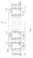
- FIG. 1shows an exemplary series-connection configuration including a plurality of devices 101 - 1 - 101 -N having four data input connections, such as data input pins D 0 -D 3 and four data output connections, such as data output pins Q 0 -Q 3 connected in series.
- the configuration 100 of a plurality of devices connected in serieshas four data input ports to receive input serial data SD 0 -SD 3 at a first device 101 - 1 of the system and four data output ports to output serial data SQ 0 -SQ 3 at a last device 101 -N of the system.
- Each of the deviceshave additional pins such as input port enable IPE, output port enable OPE, clock, reset, chip select (not shown) etc. for various signals.
- Each of the series-connected devices 101 - 1 - 101 -Nhas the same structure.
- a controller(not shown) provides a group of signals including chip select CS# (not shown), serial input port enable (SIPE), serial output port enable (SOPE), clock CLK, reset RST# and other control and data information (not shown) to the devices.
- the configuration 100 shown in FIG. 1can be, for example, a plurality of memory devices connected in series and a memory controller.
- the memory controllercommunicates with the devices to control operations of the series-connected memory devices.
- the devices shown in FIG. 1each have four data input pins D 0 -D 3 and four data output pins Q 0 -Q 3 .
- the devices shown in FIG. 1are configured to operate in multi-data width modes viz., X1, X2 or X4 modes. Briefly, one or more pins for connection are used to transfer data serially through the devices according to the chosen data width mode.
- a byte of datais transferred in eight clock cycles in the X1 mode using a single set of pins (default D 0 and Q 0 ); four clock cycles in the X2 mode using a two sets of pins (default D 0 , D 1 and Q 0 , Q 1 ), and two clock cycles in the X4 mode using all pins (D 0 -D 3 and Q 0 -Q 3 ).
- the multi-data width modeswill be discussed in detail below with reference to FIGS. 9A and 9B .
- the configuration 100 of the devices 101 - 1 - 101 -N in FIG. 1includes both series-connections (e.g., serial input and output) and conventional multi-drop connections (e.g., CLK and RST#).
- series-connectionse.g., serial input and output
- conventional multi-drop connectionse.g., CLK and RST#
- the configurationmay be referred to as a hybrid connection configuration, where the advantages of each of the series-connection and multi-drop connection may be realized.
- FIG. 2Aillustrates timing configurations during normal operation of a device in the configuration 100 of FIG. 1 , showing signals transferred between the devices.
- a chip select signal CS#(not shown) is first asserted to select the devices.
- the reset signal RST#is held high for maintaining all devices in a normal state.
- Informationis transmitted to the first device 101 - 1 in the plurality of devices connected in series by asserting SIPE and clocking data through data input pins D 0 -D 3 of device 101 - 1 on successive rising edges of the clock signal CLK.
- An input port enable signal SIPEis propagated through the first device 101 - 1 to the second device 101 - 2 from the IPEQ pin of the first device 101 - 1 to the IPE input of the second device 101 - 2 . This process is repeated for successive devices in the system of devices connected series.
- control signalsare synchronized with the rising (or falling) edge of the signal CLK in order to ensure a proper setup time for these signals at the next device in the system of devices connected in series.
- routine memory operationsare executed on a device using command strings that are serially fed to the devices.
- the command stringstypically contain a command that represents the operation to be selected, as well as other parameters.
- the operation to be performedmay be indicated in an operation (OP) code that is provided to the devices.
- OPoperation
- a write operationcan be executed by serially feeding an information string that contains a write command, the data to be written and an address in the memory to the device where the data is to be written.
- the command stringis fed to all of the devices even though the command is executed on only one of the devices.
- the command stringcontains a device identifier (ID) that identifies the device to which the command is directed.
- IDdevice identifier
- Each device receiving the command stringcompares the device ID contained in the command string to an ID associated with the device. If the two match, the device assumes that the command is directed to the device and performs the command.
- FIG. 2Billustrates timing configurations during normal command operation of a device of FIG. 1 showing signals transferred between the devices.
- the unselected devicestake input data, which is a command string containing device ID and OP code, through the input pins D 0 -D 3 and send it to the next or forward device in the system of devices connected in series, if SIPE signal is in a ‘high’ state.
- input datawhich is a command string containing device ID and OP code
- the plurality of devices connected in serieshas input ports in the first device and output ports in the last device.
- a data channelcan be defined as a data path between corresponding pairs of input and output ports.
- dataIn order for the plurality of devices connected in series to properly function, data must be propagated through the data channels from the first device to the last device in the system. Faults within a device or in the interconnection between devices connected in series will result in data not being transferred along a data path and hence result in the loss of use of a data channel.
- FIG. 3is an illustration of possible fault locations on a device and in the interconnection between devices in a configuration 200 of devices connected in series. Similar to FIG. 1 , devices 201 - 1 - 201 -N are connected in series as shown. The input/output pins and the control pins in the system 200 are similar to the configuration 100 of FIG. 1 . However, as shown in FIG. 3 , there is a line defect (interconnection defect) in the connection of output pin Q 1 of device 201 - 2 and the corresponding input pin of the next device (not shown). In addition, there are internal faults in the first device 201 - 1 of the system 200 . A person of skill in the art will appreciate that defects other than those shown in FIG. 3 are possible.
- the device 201 - 1is shown in further detail at the bottom of FIG. 3 .
- data from the input pins D 0 -D 3flows to the output pins Q 0 -Q 3 through the internal circuitry as shown, for example, by dashed line between input pin D 2 and corresponding output pin Q 2 in FIG. 3 .
- the internal circuitrycomprises for example, buffers, D-flip flops (single bit data registers), selectors etc., and is controlled by a data processor 210 and a shift register 240 .
- the exemplary device 201 - 1there are multiple defects, such as in the D-flip flop 242 and selector 244 , in the internal data path between the input pin D 1 and the corresponding output pin Q 1 , as shown by the shaded regions in FIG. 3 .
- the buffer 246 prior to the output pin Q 3is defective. These defects result in loss of data transmission in data channels through D 1 -Q 1 and D 3 -Q 3 in the configuration 200 .
- FIG. 4is an illustration of an apparatus for testing of a data channel in a system of devices connected in series in accordance with an embodiment of the present invention.
- devices 301 - 1 - 301 -Nare connected in series.
- the system 300is similar to those described with reference to FIGS. 1 and 3 .
- the devices 301 - 1 - 301 -Nhave four data input pins D 0 -D 3 and four data output pins Q 0 -Q 3 connected in series.
- the system 300 of devices connected in serieshas four data input ports to receive input serial data SD 0 -SD 3 at the first device 301 - 1 of the system and four data output ports to output serial data SQ 0 -SQ 3 at the last device 301 -N of the system.
- Each of the deviceshave additional pins such as input port enable IPE, output port enable OPE, clock, reset, chip select (not shown) etc. for various signals.
- Each of the series-connected devices 301 - 1 - 301 -Nhas the same structure.
- Each of the devices in the system 300has a data processor 310 , which will be described below with reference to FIG. 6 . As described earlier, the system of FIG. 4 is capable of being operated in multi-data width modes (X1/X2/X4 modes).
- a controller 305provides a group of signals including serial input port enable (SIPE), serial output port enable (SOPE), clock CLK and other control and data information (not shown) to the devices.
- the controller 305is for example, a memory controller.
- the controller 305also includes a data processor 350 , a data register 352 , a pattern generator 354 , a comparator 356 , a read data storage 358 and pins to receive the input port enable signal SIPEQ, the output port enable signal SOPEQ, and the output serial data SQ 0 -SQ 3 from the last of the devices (device 301 -N) connected in series. Individual elements of the controller 305 will be described in detail below.
- FIG. 5is an illustration of a method for testing of a data channel in a system of devices connected in accordance with an embodiment of the present invention.
- the controller 305upon entering a test mode (S 501 ), applies a test pattern as an input serial data SD 0 -SD 3 to data input pins D 0 -D 3 , which act as a plurality of input ports, at the first device 301 - 1 of the system 300 of devices connected in series (S 502 ).
- the plurality of input ports at the first device 301 - 1has a corresponding plurality of output ports, corresponding to data output pins Q 0 -Q 3 , at the last device 301 -N of the system 300 .
- the data channelbetween corresponding pairs of input and output ports, is enabled (S 504 ) if the test pattern is detected (S 503 ) at its corresponding output port.
- the data channelis determined to have failed (S 505 ) if the test pattern is not detected at it corresponding output port.
- the test modeis exited (S 506 ).
- FIG. 6is an example of a method for testing of input/output buffer path in the series-connected devices having a four data pins (input and output pins) and capable of operating in multi-data width modes (X1/X2/X4 modes) in accordance with an embodiment of the present invention.
- the maximum data width modeis X4 (4-bit inputs).
- high data width modesfor example, 8-bit or 16-bit are possible according to the system requirements.
- a command string propagated in the system of devices connected in seriescontains a device ID that identifies the device to which the command is directed.
- ID assignmentsare done prior to any normal operations in the system of devices connected in series.
- the assigned IDsare initialized or reset in each device prior to enabling the data channels in the system.
- the assigned IDscan be reset to ‘00’ for all devices, by using a commonly connected hard reset pin (RST#, low enable) (S 602 ). This enables the selection of all devices at once.
- the hard resetcan also initialize use-state registers in each of the device of the system of series-connected devices to a default disabled state.
- the test modeis entered by simultaneously asserting input port enable SIPE and output port enable SOPE control signals (S 603 ).
- SIPE and SOPEare simultaneously asserted all input and output ports are accessible at the same time. All input ports receive input command from the controller as if each port is simultaneously operating in a X1 mode irrespective of previous data width setting. Typically, in normal operation mode, SIPE and SOPE are not asserted simultaneously.
- data flowis typically truncated at the device where a device ID match is found.
- Subsequent (or forward) devices in the systemdo not receive the input stream except for ID bits.
- the systemcan be forced into a situation where none of the devices in the system is selected.
- the input streamtraverses all the devices in the system of devices connected in series.
- a test pattern with a ‘non-00’ IDis applied to the input pins D 0 -D 3 of the first device 301 - 1 of the system (S 604 ). As described above, the test pattern flows through system of devices connected in series since no particular device is selected. Test patterns, such as checkerboard, scan zero, scan one etc. can be applied to the system. Once the test pattern has propagated through the system, the output patterns at the output pins Q 0 -Q 3 of the last device 301 -N of the system are detected (S 605 ). If the test pattern is not detected in any of the data channels (S 606 ), then the system is determined to have “failed” (S 607 ).
- test patternis detected in all the data channels (S 608 )
- the systemis determined to have “passed” (S 609 ).
- the systemmay still be able to operate in X1 or X2 mode and further determination of which of the data channels corresponding to D 0 -D 3 pins are defective is made (S 610 , S 612 , S 614 , S 616 ).
- the pins corresponding to “failed” data channelsare determined to be of no use (S 611 , S 613 , S 615 , S 617 ).
- the possible combinations of pins for X1 or X2 data width modeare determined (S 618 ).
- a data mode configuration register in each of the devices and the controlleris accordingly updated (S 619 ).
- All pins corresponding to “passed” data channelsare enabled by setting the corresponding use-state registers (S 620 ), in each of the devices in the system, to an enabled mode.
- S 620Upon setting of use-state registers (S 620 ), determination of the system being passed (S 609 ) or determination of the system being failed (S 607 ), the test mode exits (S 621 ) and the testing is stopped (S 622 ).
- the system of devices connected in seriescan be operated at multi-data widths, the physical pin connection on the system board determines the maximum data width. For example, although the devices 301 - 1 - 301 -N can be operated in the X4 mode, if there are only 2 physical pin connections in the system board, the devices can only be operated in the X2 mode.
- the pattern generator 354 of the controller 305can be used to generate and provide the test pattern to the input pins.
- the controller 305outputs the test pattern based on a test_mode signal provided by the data processor 350 .
- the comparator 356 of the controller 305can compare the output patterns and determine whether a data channel is defective or not.
- the controller 305outputs the contents of the data register 352 .
- the output serial data or output data stream SQ 0 -SQ 3is typically stored in the read data storage 358 .
- a controller with a pattern generator and comparatordoes not demand large area and its area penalty within conventional controller is negligible.
- data channel test resultsare categorized as two parts when X4 is a maximum physical data width limited by interconnection lines.
- the systemcan be operated in X2 and X1 modes only.
- two data channelsare required. Therefore, in the event that only one data channel fails in a system having four data channels, there is a redundant data channel that is not used. For example, as shown in the last four rows of Table 1, only two of the three “passed” pins are used in the X2 mode.
- FIG. 7Ais an illustration of a timing diagram to activate test mode in accordance with an embodiment of the present invention.
- the device IDs of all the devices in the system of device connected in seriesare initialized using the reset RST# signal.
- the test modecan be activated by simultaneously asserting SIPE and SOPE.
- the test patternis applied to the input pins D 0 -D 3 while continuing to assert SIPE and SOPE as shown in FIG. 7A .
- the SIPE and SOPEare asserted for predetermined number of clock cycles (for example, 10 cycles) prior to applying the test patterns to the input pins.
- the controller 305knows the pins corresponding to “passed” data channels.
- the use-state registers corresponding to these pinswill now have to be enabled from the default value assigned to the registers prior to the start of the test mode operation.
- the controller 305issues a command (for example, Passed I/O set command) that sets a use state of the pins corresponding to the “passed” data channels in all the devices in the system of devices connected in series. Due to the reset operation prior to entering the test mode operation, all devices have the same ‘00’ IDs, as described earlier.
- FIG. 7Bis an illustration of a timing configuration during a passed I/O command assertion operation in accordance with an embodiment of the present invention.
- SIPE and SOPEare simultaneously asserted, all the devices in the system of devices connected in series function in X1 mode, ignoring the setting of a device configuration register (to be discussed with reference to FIG. 8 ) that contains device I/O configurations such as data mode configuration.
- Only pins corresponding to “passed” data channelcan receive and accept ‘Pass I/O set command’ and the use-state registers associated with those pins are enabled until power-down. Power-down and power-up can reset the setting of the use-state or the Pass I/O set command bit in the use state register of the devices.
- the pins corresponding to “failed” data channelscannot propagate any input streams to the next device so that initially set default disabled state of the use-state registers are maintained.
- Both the test mode operation and the enabling of pins and setting of the corresponding use state registersare activated by simultaneously asserting SIPE and SOPE (see FIGS. 7A and 7B ).
- ID number and dummy cyclesare used.
- a ‘00’ ID numberis used along with a 2-bit code ‘11’ for setting the use-state of the pins corresponding to “passed” data channels (for example, D 0 and D 3 in FIG. 7B ).
- a non-zero ID and 2-bit code ‘00’is used for setting the use-state of the pins corresponding to “failed” data channels (for example, D 1 and D 2 in FIG. 7B ).
- FIG. 8is a schematic representation of the data processor of a device shown in FIG. 4 in accordance with an embodiment of the present invention.
- the data processor 310is similar to the data processor 210 shown in FIG. 3 .
- the data processor 310includes an input/output controller 312 , a pass I/O set command decoder 314 , an I/O switch control logic 316 , a use-state register 318 and a data mode configuration register 320 .
- the device processor 310also includes various registers such as ID register 322 for storing the device ID, an operation register 324 for storing OP codes, address register 326 for storing the device address, input data register 328 for storing input data, clock generator 330 for generating clock signals for the various registers, and main logic execution circuitry 332 that controls the overall operation and logic of the device. All registers described above are flexible and capable of receiving multi-data width inputs.
- the input/output controller 312receives the ipei and opei signals corresponding to the SIPE and SOPE signals and issues a tm_en (test mode enable) signal during test mode operation.
- the SIPE and SOPE signalsare provided to the input/output controller 312 either directly or indirectly from the controller 305 .
- the first device 301 - 1receives, at its IPE and OPE pins, the SIPE and SOPE signals directly from the controller 305 .
- Subsequent devices, 301 - 2 to 301 -Nreceive SIPE and SOPE signals propagated through the system of devices connected in series.
- Input data id 0 -id 3corresponding to input serial data SD 0 -SD 3 , is decoded during a test mode/pass I/O set command operation in response to the tm_en signal.
- the first device 301 - 1receives, at its input pins D 0 -D 3 , input serial data SD 0 -SD 3 directly from the controller 305 .
- Subsequent devices, 301 - 2 to 301 -N,receive input serial data SD 0 -SD 3 propagated through the system of devices connected in series.
- the I/O switch control logic 316issues the switch logic control signals S 1 -S 4 that determine the data width mode (X1/X2/X4 mode) as shown in FIG. 9B .
- the I/O switch control logic 316also sets the use-state registers 318 to indicate status the pins that correspond to “passed” data channels and the data mode configuration register 320 .
- the clock generator 330receives an internal clock signal iclk that is derived from the clock signal CLK for generating clock signals for the various controllers, registers, etc of the data processor 310 .
- Table 2shows the truth table of switch logic output control signals S 1 -S 4 depending on the fail and pass combinations shown in Table 1.
- X1 and X2 mode controlsare performed with different control signals as shown in FIG. 9B .
- FIG. 9Ais an illustration of operation of a device shown in FIG. 4 in multi-data width modes (X1/X2/X4 modes) using input pins (D 0 -D 3 ) and corresponding output pins (Q 0 -Q 3 ) in accordance with an embodiment of the present invention.
- a byte of datais transferred in eight clock cycles in the X1 mode using a single set of pins (default D 0 and Q 0 ); four clock cycles in the X2 mode using a two sets of pins (default D 0 , D 1 and Q 0 , Q 1 ), and two clock cycles in the X4 mode using all pins (D 0 -D 3 and Q 0 -Q 3 ).
- the default pin assignmentscan be changed after the test mode operation determines that certain pins are not usable.
- a reassignment of the pins assigned for X1 or X2 modecan be made based on the status of the use-state registers 318 , data mode configuration register 320 , and the switch logic control signals S 1 -S 4 .
- switch control logic circuitbased on Table 2 is shown in FIG. 9B .
- X4/X2/X1 signalsare generated from the data mode configuration register 320 .
- Two modes(X2/X1) are available if any one of the data channels fails. According to the number of failed data channels, X1 mode or X2 mode is determined.
- the possibility of malfunction due to hard-defects on relevant logic and interconnections of input/output pinsis not high, but if malfunction occurs while devices are being used, all modules on a system board are generally replaced. Replacement cost of all the modules or the entire system board is much higher than the replacement of a single device and data recovery from the failed device or system board may be impossible.
- the embodiments disclosed hereincan allow cost reduction and provides more stable operating condition to the system. Using the embodiments disclosed herein, cumulative yield of device production, without many additional circuit implementations into the device, could be increased (more devices can be used even though operation at maximum data width configuration may not be possible).
- the embodiments described hereinalso enable the recovery of any data on a failed device in the system of devices connected in series.
- datacan be recovered from failed hard disks, such as in Solid State Disk (SSD) based on flash memory.
- SSDSolid State Disk
- SSD reliability and durabilityare much better than the hard disk that consists of mechanical parts like rapidly rotating platters and a motor. But, accidental damage or wearing out of routes or pins cannot be avoided and can result in the non-data recovery in SSD system.
- the embodiment disclosed hereinresolves those problems without removing parts or breaking up the board or system parts.
- Embodiments of the inventioncan be represented as a software product stored in a machine-readable medium (also referred to as a computer-readable medium, a processor-readable medium, or a computer usable medium having a computer-readable program code embodied therein).
- the machine-readable mediumcan be any suitable tangible medium, including magnetic, optical, or electrical storage medium including a diskette, compact disk read only memory (CD-ROM), memory device (volatile or non-volatile), or similar storage mechanism.
- the machine-readable mediumcan contain various sets of instructions, code sequences, configuration information, or other data, which, when executed, cause a processor to perform steps in a method according to an embodiment of the invention.
- Those of ordinary skill in the artwill appreciate that other instructions and operations necessary to implement the described invention can also be stored on the machine-readable medium.
- Software running from the machine-readable mediumcan interface with circuitry to perform the described tasks.
Landscapes
- Tests Of Electronic Circuits (AREA)
- Test And Diagnosis Of Digital Computers (AREA)
Abstract
Description
- This application is a Continuation of U.S. patent application Ser. No. 12/028,335, filed on Feb. 8, 2008, which claims the benefit of priority from U.S. Provisional Patent Application No. 60/989,879, filed on Nov. 23, 2007.
- The present invention relates generally to the testing of a system having a plurality of devices. More particularly, the present invention relates to the testing of data channels in a system of devices connected in series.
- Semiconductor memory devices are important components in presently available industrial and consumer electronics products. For example, computers, mobile phones, and other portable electronics all rely on some form of memory for storing data. While many memory devices are typically available as commodity devices, the need for higher integration has led to the development of embedded memory, which can be integrated with systems, such as microcontrollers and other processing circuits.
- Unfortunately, the density of commodity memory cannot match the ever-increasing demand for memory. Hence multiple commodity memories are used together to fulfill the system memory requirements. Multi-device memory systems can be implemented as a set of silicon chips grouped together in a single package (called a multi chip system-MCP), or a multiplicity of memory device packages grouped together on a printed circuit board.
- More often, the multi-device memory systems employ, non-volatile devices, such as flash devices, for storage. Demand for flash memory devices has continued to grow significantly because these devices are well suited in various embedded applications that require non-volatile storage. For example, flash is widely used in various consumer devices, such as digital cameras, cell phones, USB flash drives and portable music players, to store data used by these devices. Market demand for flash memory has led to tremendous improvements in flash memory technology over the past several years both in terms of speed and density.
- Some flash devices employ serial interfaces such as, for example, multiple flash devices, which are used to perform operations, such as read, write and erase operations, on memory contained in the devices. A system of devices connected in series has input ports in the first device and output ports in the last device as shown in
FIG. 1 . Data is serially transferred from the input ports in the first device to the output ports in the last device. The configuration of the series-connected devices shown inFIG. 1 will be discussed in detail below. - Those skilled in the art understand that multi-device systems are tested at the individual component level and at the system level to ensure robustness of operation. In particular, memory devices are tested at the chip level to ensure that their memory cells are not defective. A defective memory cell is one that does not store data properly, due to fabrication defects or other defects that may occur during fabrication or assembly of the memory device.
- Although each device is tested through functional and DC test steps at wafer-level and package level to screen out the device with defects on memory or logic blocks, it is difficult to find which devices have failed once they are mounted on the system board after packaging with stacked devices in a series-connection configuration. In conjunction with this problem, if there were any single failed device in the system of devices connected in series, all devices on the connection would be shown as defective devices due to data transmission failure caused by the failed device.
- Typically, a fault in any single pin or in the interconnection between devices in the system of devices connected in series causes all devices to be judged as “failed” and no more testing is possible. Needless to say that the cost of stacked devices is much higher than the cost of a single device, and even good devices without any faults could be thrown away, or a system board with these devices may be replaced with a new one.
- An apparatus and method for testing and enabling data channels path in a system of devices connected in series is disclosed. The devices are, for example, memory devices, such as dynamic random access memories (DRAMs), static random access memories (SRAMs) and flash memories.
- According to an aspect of the present invention, there is provided a method for enabling data channels in series-connected devices. The method comprises applying a test pattern to a plurality of input ports at a first device of the series-connected devices. The plurality of input ports has a corresponding plurality of output ports at a last device of the series-connected devices. Each data channel defines a data path between corresponding pairs of input and output ports. The method also comprises enabling a data channel if the test pattern is detected at its corresponding output port.
- According to another aspect of the present invention, there is provided a device for use in a system of a plurality of devices connected in series and a controller. The device comprises a plurality of input connections and corresponding plurality of output connections; a plurality of use-state registers associated with each of the corresponding input and output connections to indicate a use-state of the corresponding input and output connections; and a data mode configuration register to indicate the maximum data width for transmission through the device.
- According to another aspect of the present invention, there is provided a controller for enabling data channels in a plurality of devices connected in series. The controller comprises a test pattern generator for providing a test pattern to a plurality of input ports at a first device of the plurality of devices connected in series. The plurality of input ports has a corresponding plurality of output ports at a last device of the plurality of devices connected in series. Each data channel defines a data path between corresponding pairs of input and output ports of the plurality of devices connected in series in a data channel test operation. The controller enables data channels if the test pattern is detected at its corresponding output port.
- According to another aspect of the present invention, there is provided a system comprising a plurality of devices, having a plurality of data channels, connected in series. The plurality of devices has a plurality of input ports at a first device of the plurality of devices connected in series. The plurality of input ports has a corresponding plurality of output ports at a last device of the plurality of devices connected in series. Each data channel defines a data path between corresponding pairs of input and output ports. The system also comprises a controller coupled to the plurality of input ports and the corresponding plurality of output ports. The controller has a test pattern generator for providing a test pattern to the plurality of input ports in a data channel test operation. The controller enables data channels if the test pattern is detected at its corresponding output port.
- Other aspects and features of the present invention will become apparent to those ordinarily skilled in the art upon review of the following description of specific embodiments of the invention in conjunction with the accompanying figures.
- Embodiments of the present invention will now be described, by way of example only, with reference to the attached Figures, wherein:
FIG. 1 is an illustration of a plurality of devices connected in series;FIG. 2A is an illustration of a timing configuration during normal operation of a device ofFIG. 1 ;FIG. 2B is an illustration of a timing configuration during a normal command operation of a device ofFIG. 1 ;FIG. 3 is an illustration of possible fault locations on a device and in the interconnection between devices in a plurality of devices connected in series;FIG. 4 is an illustration of an apparatus for testing of a data channel in a system of devices connected in series in accordance with an embodiment of the present invention;FIG. 5 is an illustration of a method for testing of a data channel in a system of devices connected in accordance with an embodiment of the present invention;FIG. 6 is an example of a method for testing of input/output buffer path in series-connected devices having a four data pins (input and output pins) and capable of operating in multi-data width modes (X1/X2/X4 modes) in accordance with an embodiment of the present invention;FIG. 7A is an illustration of a timing diagram to activate test mode with IPE and OPE in accordance with an embodiment of the present invention;FIG. 7B is an illustration of a timing configuration during a passed I/O command assertion operation in accordance with an embodiment of the present invention.FIG. 8 is a schematic representation of the data processor of a device shown inFIG. 4 in accordance with an embodiment of the present invention;FIG. 9A is an illustration of operation of a device shown inFIG. 4 in multi-data width modes (X1/X2/X4 modes) using input pins (D0-D3) and corresponding output pins (Q0-Q3) in accordance with an embodiment of the present invention; andFIG. 9B is an illustration of configuration internal registers for multi-data width modes (X1/X2/X4 modes) in accordance with an embodiment of the present invention;- Generally, the present invention provides a system of devices connected in series. An apparatus and a method for testing of data channels in a system of devices connected in series are disclosed.
- The method and apparatus in accordance with the techniques described herein may be applicable to a memory system having a plurality of devices connected in series. The devices are, for example, memory devices, such as dynamic random access memories (DRAMs), static random access memories (SRAMs) and flash memories.
FIG. 1 shows an exemplary series-connection configuration including a plurality of devices101-1-101-N having four data input connections, such as data input pins D0-D3 and four data output connections, such as data output pins Q0-Q3 connected in series. Theconfiguration 100 of a plurality of devices connected in series has four data input ports to receive input serial data SD0-SD3 at a first device101-1 of the system and four data output ports to output serial data SQ0-SQ3 at a last device101-N of the system. Each of the devices have additional pins such as input port enable IPE, output port enable OPE, clock, reset, chip select (not shown) etc. for various signals. Each of the series-connected devices101-1-101-N has the same structure. A controller (not shown) provides a group of signals including chip select CS# (not shown), serial input port enable (SIPE), serial output port enable (SOPE), clock CLK, reset RST# and other control and data information (not shown) to the devices. Theconfiguration 100 shown inFIG. 1 can be, for example, a plurality of memory devices connected in series and a memory controller. The memory controller communicates with the devices to control operations of the series-connected memory devices.- The devices shown in
FIG. 1 each have four data input pins D0-D3 and four data output pins Q0-Q3. As such, the devices shown inFIG. 1 are configured to operate in multi-data width modes viz., X1, X2 or X4 modes. Briefly, one or more pins for connection are used to transfer data serially through the devices according to the chosen data width mode. For example, a byte of data is transferred in eight clock cycles in the X1 mode using a single set of pins (default D0 and Q0); four clock cycles in the X2 mode using a two sets of pins (default D0, D1 and Q0, Q1), and two clock cycles in the X4 mode using all pins (D0-D3 and Q0-Q3). The multi-data width modes will be discussed in detail below with reference toFIGS. 9A and 9B . - The
configuration 100 of the devices101-1-101-N inFIG. 1 includes both series-connections (e.g., serial input and output) and conventional multi-drop connections (e.g., CLK and RST#). Thus, the configuration may be referred to as a hybrid connection configuration, where the advantages of each of the series-connection and multi-drop connection may be realized. FIG. 2A illustrates timing configurations during normal operation of a device in theconfiguration 100 ofFIG. 1 , showing signals transferred between the devices. A chip select signal CS# (not shown) is first asserted to select the devices. In the exemplary operation shown inFIG. 2A , the reset signal RST# is held high for maintaining all devices in a normal state. Information is transmitted to the first device101-1 in the plurality of devices connected in series by asserting SIPE and clocking data through data input pins D0-D3 of device101-1 on successive rising edges of the clock signal CLK. An input port enable signal SIPE is propagated through the first device101-1 to the second device101-2 from the IPEQ pin of the first device101-1 to the IPE input of the second device101-2. This process is repeated for successive devices in the system of devices connected series. Typically, control signals are synchronized with the rising (or falling) edge of the signal CLK in order to ensure a proper setup time for these signals at the next device in the system of devices connected in series.- Typically, in a system of memory devices connected in series, routine memory operations are executed on a device using command strings that are serially fed to the devices. The command strings typically contain a command that represents the operation to be selected, as well as other parameters. The operation to be performed may be indicated in an operation (OP) code that is provided to the devices. For example, a write operation can be executed by serially feeding an information string that contains a write command, the data to be written and an address in the memory to the device where the data is to be written.
- For example, the command string is fed to all of the devices even though the command is executed on only one of the devices. For a particular example, to select the device on which the command is to be performed, the command string contains a device identifier (ID) that identifies the device to which the command is directed. Each device receiving the command string compares the device ID contained in the command string to an ID associated with the device. If the two match, the device assumes that the command is directed to the device and performs the command. Thus, input data are transmitted to the selected device without execution of the OP code in the unselected devices.
FIG. 2B illustrates timing configurations during normal command operation of a device ofFIG. 1 showing signals transferred between the devices. For example, the unselected devices take input data, which is a command string containing device ID and OP code, through the input pins D0-D3 and send it to the next or forward device in the system of devices connected in series, if SIPE signal is in a ‘high’ state. - As discussed earlier, the plurality of devices connected in series has input ports in the first device and output ports in the last device. A data channel can be defined as a data path between corresponding pairs of input and output ports. In order for the plurality of devices connected in series to properly function, data must be propagated through the data channels from the first device to the last device in the system. Faults within a device or in the interconnection between devices connected in series will result in data not being transferred along a data path and hence result in the loss of use of a data channel.
FIG. 3 is an illustration of possible fault locations on a device and in the interconnection between devices in aconfiguration 200 of devices connected in series. Similar toFIG. 1 , devices201-1-201-N are connected in series as shown. The input/output pins and the control pins in thesystem 200 are similar to theconfiguration 100 ofFIG. 1 . However, as shown inFIG. 3 , there is a line defect (interconnection defect) in the connection of output pin Q1 of device201-2 and the corresponding input pin of the next device (not shown). In addition, there are internal faults in the first device201-1 of thesystem 200. A person of skill in the art will appreciate that defects other than those shown inFIG. 3 are possible.- The device201-1 is shown in further detail at the bottom of
FIG. 3 . Typically, data from the input pins D0-D3 flows to the output pins Q0-Q3 through the internal circuitry as shown, for example, by dashed line between input pin D2 and corresponding output pin Q2 inFIG. 3 . The internal circuitry comprises for example, buffers, D-flip flops (single bit data registers), selectors etc., and is controlled by adata processor 210 and ashift register 240. In the exemplary device201-1, there are multiple defects, such as in the D-flip flop 242 andselector 244, in the internal data path between the input pin D1 and the corresponding output pin Q1, as shown by the shaded regions inFIG. 3 . Similarly, thebuffer 246 prior to the output pin Q3 is defective. These defects result in loss of data transmission in data channels through D1-Q1 and D3-Q3 in theconfiguration 200. - In conventional wafer-level and package level testing, faults within a device or in the interconnection between devices connected in series, such as those illustrated in
FIG. 3 , will result in all devices on the connection to be shown as defective devices and the entire system to be discarded. However, as shown inFIG. 3 , data transmission can occur in data channels through D0-Q0 and D2-Q2, and theconfiguration 200 can be operated in X1 and X2 modes. The internal defects and the line defects can be indentified using embodiments of the invention disclosed herein and data channels without any defects can be enabled for use by the plurality of devices connected in series. FIG. 4 is an illustration of an apparatus for testing of a data channel in a system of devices connected in series in accordance with an embodiment of the present invention. In thesystem 300, devices301-1-301-N are connected in series. Thesystem 300 is similar to those described with reference toFIGS. 1 and 3 .- The devices301-1-301-N have four data input pins D0-D3 and four data output pins Q0-Q3 connected in series. The
system 300 of devices connected in series has four data input ports to receive input serial data SD0-SD3 at the first device301-1 of the system and four data output ports to output serial data SQ0-SQ3 at the last device301-N of the system. Each of the devices have additional pins such as input port enable IPE, output port enable OPE, clock, reset, chip select (not shown) etc. for various signals. Each of the series-connected devices301-1-301-N has the same structure. Each of the devices in thesystem 300 has adata processor 310, which will be described below with reference toFIG. 6 . As described earlier, the system ofFIG. 4 is capable of being operated in multi-data width modes (X1/X2/X4 modes). - A
controller 305 provides a group of signals including serial input port enable (SIPE), serial output port enable (SOPE), clock CLK and other control and data information (not shown) to the devices. Thecontroller 305, is for example, a memory controller. Thecontroller 305 also includes adata processor 350, adata register 352, apattern generator 354, acomparator 356, aread data storage 358 and pins to receive the input port enable signal SIPEQ, the output port enable signal SOPEQ, and the output serial data SQ0-SQ3 from the last of the devices (device301-N) connected in series. Individual elements of thecontroller 305 will be described in detail below. FIG. 5 is an illustration of a method for testing of a data channel in a system of devices connected in accordance with an embodiment of the present invention. Generally, upon entering a test mode (S501), thecontroller 305 applies a test pattern as an input serial data SD0-SD3 to data input pins D0-D3, which act as a plurality of input ports, at the first device301-1 of thesystem 300 of devices connected in series (S502). The plurality of input ports at the first device301-1 has a corresponding plurality of output ports, corresponding to data output pins Q0-Q3, at the last device301-N of thesystem 300. The data channel, between corresponding pairs of input and output ports, is enabled (S504) if the test pattern is detected (S503) at its corresponding output port. The data channel is determined to have failed (S505) if the test pattern is not detected at it corresponding output port. Once all data channels have been enabled (or disabled), the test mode is exited (S506).FIG. 6 is an example of a method for testing of input/output buffer path in the series-connected devices having a four data pins (input and output pins) and capable of operating in multi-data width modes (X1/X2/X4 modes) in accordance with an embodiment of the present invention. For the purposes of this discussion, the maximum data width mode is X4 (4-bit inputs). However, it will be readily apparent to those skilled in the art that high data width modes (for example, 8-bit or 16-bit) are possible according to the system requirements.- As described earlier, a command string propagated in the system of devices connected in series contains a device ID that identifies the device to which the command is directed. Typically, ID assignments are done prior to any normal operations in the system of devices connected in series. In an exemplary embodiment of the present invention, during test mode (S601), the assigned IDs are initialized or reset in each device prior to enabling the data channels in the system. For example, the assigned IDs can be reset to ‘00’ for all devices, by using a commonly connected hard reset pin (RST#, low enable) (S602). This enables the selection of all devices at once. The hard reset can also initialize use-state registers in each of the device of the system of series-connected devices to a default disabled state.
- The test mode is entered by simultaneously asserting input port enable SIPE and output port enable SOPE control signals (S603). When SIPE and SOPE are simultaneously asserted all input and output ports are accessible at the same time. All input ports receive input command from the controller as if each port is simultaneously operating in a X1 mode irrespective of previous data width setting. Typically, in normal operation mode, SIPE and SOPE are not asserted simultaneously.
- In a system of devices connected in series, data flow is typically truncated at the device where a device ID match is found. Subsequent (or forward) devices in the system do not receive the input stream except for ID bits. However, by initializing the device IDs of the all the devices in the system to a common known value (for example, ‘00’) and by propagating a ‘non-00’ ID (no match), the system can be forced into a situation where none of the devices in the system is selected. Thus, the input stream traverses all the devices in the system of devices connected in series.
- A test pattern with a ‘non-00’ ID, is applied to the input pins D0-D3 of the first device301-1 of the system (S604). As described above, the test pattern flows through system of devices connected in series since no particular device is selected. Test patterns, such as checkerboard, scan zero, scan one etc. can be applied to the system. Once the test pattern has propagated through the system, the output patterns at the output pins Q0-Q3 of the last device301-N of the system are detected (S605). If the test pattern is not detected in any of the data channels (S606), then the system is determined to have “failed” (S607). However, if the test pattern is detected in all the data channels (S608), the system is determined to have “passed” (S609). In the event that the test pattern is detected in some but not all the data channels, it is determined that the system cannot operate in the X4 mode. However, the system may still be able to operate in X1 or X2 mode and further determination of which of the data channels corresponding to D0-D3 pins are defective is made (S610, S612, S614, S616). The pins corresponding to “failed” data channels are determined to be of no use (S611, S613, S615, S617). Based on the number of “passed” data channels, the possible combinations of pins for X1 or X2 data width mode are determined (S618). A data mode configuration register in each of the devices and the controller is accordingly updated (S619).
- All pins corresponding to “passed” data channels are enabled by setting the corresponding use-state registers (S620), in each of the devices in the system, to an enabled mode. Upon setting of use-state registers (S620), determination of the system being passed (S609) or determination of the system being failed (S607), the test mode exits (S621) and the testing is stopped (S622). It should be noted that although the system of devices connected in series can be operated at multi-data widths, the physical pin connection on the system board determines the maximum data width. For example, although the devices301-1-301-N can be operated in the X4 mode, if there are only 2 physical pin connections in the system board, the devices can only be operated in the X2 mode.
- In the above-described embodiment, the
pattern generator 354 of thecontroller 305, can be used to generate and provide the test pattern to the input pins. Thecontroller 305 outputs the test pattern based on a test_mode signal provided by thedata processor 350. In addition, thecomparator 356 of thecontroller 305 can compare the output patterns and determine whether a data channel is defective or not. In normal mode operation, thecontroller 305 outputs the contents of the data register352. During normal mode operation, the output serial data or output data stream SQ0-SQ3 is typically stored in theread data storage 358. A controller with a pattern generator and comparator does not demand large area and its area penalty within conventional controller is negligible. - According to Table 1, data channel test results are categorized as two parts when X4 is a maximum physical data width limited by interconnection lines. As described earlier, when the test pattern is not detected in one or more data channels, the system can be operated in X2 and X1 modes only. In order for the system to be operated in X2 mode, two data channels are required. Therefore, in the event that only one data channel fails in a system having four data channels, there is a redundant data channel that is not used. For example, as shown in the last four rows of Table 1, only two of the three “passed” pins are used in the X2 mode.
TABLE 1 Passed Input/output mode assignment D3/Q3 D2/Q2 D1/Q1 D0/Q0 Data width setting X X X O X1 mode X X O X X O X X O X X X X X O O X2 mode X O X O (O1= two input pins O X X O used in X2 mode) X O O X O X O X O O X X X O O1 O1 O O1 X O1 O X O1 O1 O O1 O1 X FIG. 7A is an illustration of a timing diagram to activate test mode in accordance with an embodiment of the present invention. As described with reference toFIG. 6 , prior to entering the test mode, the device IDs of all the devices in the system of device connected in series are initialized using the reset RST# signal. The test mode can be activated by simultaneously asserting SIPE and SOPE. The test pattern is applied to the input pins D0-D3 while continuing to assert SIPE and SOPE as shown inFIG. 7A . In order to avoid timing conflicts with normal mode operation, the SIPE and SOPE are asserted for predetermined number of clock cycles (for example, 10 cycles) prior to applying the test patterns to the input pins.- As a result of test mode operation, the
controller 305 knows the pins corresponding to “passed” data channels. The use-state registers corresponding to these pins will now have to be enabled from the default value assigned to the registers prior to the start of the test mode operation. Thecontroller 305 issues a command (for example, Passed I/O set command) that sets a use state of the pins corresponding to the “passed” data channels in all the devices in the system of devices connected in series. Due to the reset operation prior to entering the test mode operation, all devices have the same ‘00’ IDs, as described earlier. Therefore, the Passed I/O set command to set a use state of the pins corresponding to the “passed” data channels has a ‘00’ ID number in the command string.FIG. 7B is an illustration of a timing configuration during a passed I/O command assertion operation in accordance with an embodiment of the present invention. - As described earlier, SIPE and SOPE are simultaneously asserted, all the devices in the system of devices connected in series function in X1 mode, ignoring the setting of a device configuration register (to be discussed with reference to
FIG. 8 ) that contains device I/O configurations such as data mode configuration. Only pins corresponding to “passed” data channel can receive and accept ‘Pass I/O set command’ and the use-state registers associated with those pins are enabled until power-down. Power-down and power-up can reset the setting of the use-state or the Pass I/O set command bit in the use state register of the devices. The pins corresponding to “failed” data channels cannot propagate any input streams to the next device so that initially set default disabled state of the use-state registers are maintained. - Both the test mode operation and the enabling of pins and setting of the corresponding use state registers are activated by simultaneously asserting SIPE and SOPE (see
FIGS. 7A and 7B ). In order to distinguish the two operations, ID number and dummy cycles are used. In the use-state enabling operation following the test mode, a ‘00’ ID number is used along with a 2-bit code ‘11’ for setting the use-state of the pins corresponding to “passed” data channels (for example, D0 and D3 inFIG. 7B ). On the other hand, a non-zero ID and 2-bit code ‘00’ is used for setting the use-state of the pins corresponding to “failed” data channels (for example, D1 and D2 inFIG. 7B ). FIG. 8 is a schematic representation of the data processor of a device shown inFIG. 4 in accordance with an embodiment of the present invention. Thedata processor 310 is similar to thedata processor 210 shown inFIG. 3 . Thedata processor 310 includes an input/output controller312, a pass I/O setcommand decoder 314, an I/Oswitch control logic 316, a use-state register 318 and a data mode configuration register320. Thedevice processor 310 also includes various registers such asID register 322 for storing the device ID, anoperation register 324 for storing OP codes, address register326 for storing the device address, input data register328 for storing input data,clock generator 330 for generating clock signals for the various registers, and mainlogic execution circuitry 332 that controls the overall operation and logic of the device. All registers described above are flexible and capable of receiving multi-data width inputs.- The input/output controller312 receives the ipei and opei signals corresponding to the SIPE and SOPE signals and issues a tm_en (test mode enable) signal during test mode operation. The SIPE and SOPE signals are provided to the input/output controller312 either directly or indirectly from the
controller 305. For example, the first device301-1 receives, at its IPE and OPE pins, the SIPE and SOPE signals directly from thecontroller 305. Subsequent devices,301-2 to301-N, receive SIPE and SOPE signals propagated through the system of devices connected in series. Input data id0-id3, corresponding to input serial data SD0-SD3, is decoded during a test mode/pass I/O set command operation in response to the tm_en signal. For example, the first device301-1 receives, at its input pins D0-D3, input serial data SD0-SD3 directly from thecontroller 305. Subsequent devices,301-2 to301-N, receive input serial data SD0-SD3 propagated through the system of devices connected in series. The I/Oswitch control logic 316 issues the switch logic control signals S1-S4 that determine the data width mode (X1/X2/X4 mode) as shown inFIG. 9B . The I/Oswitch control logic 316 also sets the use-state registers 318 to indicate status the pins that correspond to “passed” data channels and the data mode configuration register320. Theclock generator 330 receives an internal clock signal iclk that is derived from the clock signal CLK for generating clock signals for the various controllers, registers, etc of thedata processor 310. - Table 2 shows the truth table of switch logic output control signals S1-S4 depending on the fail and pass combinations shown in Table 1. X1 and X2 mode controls are performed with different control signals as shown in
FIG. 9B . TABLE 2 S1~S4 binary output regarding failed I/O combinations D3/Q3 D2/Q2 D1/Q1 D0/Q0 Data width S4 S3 S2 S1 X X X O X1 mode 0 0 0 0 X X O X 0 0 0 1 X O X X 0 0 1 0 O X X X 0 0 1 1 X X O O X2 mode 0 0 0 0 X O X O 0 1 0 0 O X X O 1 0 0 0 X O O X 0 1 0 1 O X O X 1 0 0 1 O O X X 1 0 1 0 X O O1 O1 0 0 0 0 O O1 X O1 0 1 0 0 O X O1 O1 0 0 0 0 O O1 O1 X 0 1 0 1 FIG. 9A is an illustration of operation of a device shown inFIG. 4 in multi-data width modes (X1/X2/X4 modes) using input pins (D0-D3) and corresponding output pins (Q0-Q3) in accordance with an embodiment of the present invention. As described earlier, a byte of data is transferred in eight clock cycles in the X1 mode using a single set of pins (default D0 and Q0); four clock cycles in the X2 mode using a two sets of pins (default D0, D1 and Q0, Q1), and two clock cycles in the X4 mode using all pins (D0-D3 and Q0-Q3). However, the default pin assignments can be changed after the test mode operation determines that certain pins are not usable. A reassignment of the pins assigned for X1 or X2 mode can be made based on the status of the use-state registers 318, data mode configuration register320, and the switch logic control signals S1-S4.- An example of switch control logic circuit based on Table 2 is shown in
FIG. 9B . X4/X2/X1 signals are generated from the data mode configuration register320. Two modes (X2/X1) are available if any one of the data channels fails. According to the number of failed data channels, X1 mode or X2 mode is determined. - The embodiments disclosed herein are described with respect to a system of devices connected in series wherein each of the devices in the system has four input /output ports to support X1/X2/X4 modes depending on system requirements. Aspects of the present invention may be applicable to systems with more than two input/output ports without any restrictions, logically and technically.
- In the above described embodiments of the present invention it is assumed that all devices in the system are connected in series as shown in
FIG. 1 or4. It is also assumed that IPE and OPE ports and internal relevant circuits along with the interconnection lines between the respective IPE/OPE pins of the devices not defective. A device with defective IPE and/or OPE pins cannot enable serial data propagation. Furthermore, it is assumed that the reset pin is not defective and can initialize the device IDs, use-state registers, and the data mode configuration during hard reset prior to test mode operation. The default mode on power-up can be set to X1 mode. - Typically, the possibility of malfunction due to hard-defects on relevant logic and interconnections of input/output pins is not high, but if malfunction occurs while devices are being used, all modules on a system board are generally replaced. Replacement cost of all the modules or the entire system board is much higher than the replacement of a single device and data recovery from the failed device or system board may be impossible. The embodiments disclosed herein can allow cost reduction and provides more stable operating condition to the system. Using the embodiments disclosed herein, cumulative yield of device production, without many additional circuit implementations into the device, could be increased (more devices can be used even though operation at maximum data width configuration may not be possible).
- The embodiments described herein also enable the recovery of any data on a failed device in the system of devices connected in series. For example, data can be recovered from failed hard disks, such as in Solid State Disk (SSD) based on flash memory. Ideally, SSD reliability and durability are much better than the hard disk that consists of mechanical parts like rapidly rotating platters and a motor. But, accidental damage or wearing out of routes or pins cannot be avoided and can result in the non-data recovery in SSD system. The embodiment disclosed herein resolves those problems without removing parts or breaking up the board or system parts.
- In the preceding description, for purposes of explanation, numerous details are set forth in order to provide a thorough understanding of the embodiments of the invention. However, it will be apparent to one skilled in the art that these specific details are not required in order to practice the invention. In other instances, well-known electrical structures and circuits are shown in block diagram form in order not to obscure the invention. For example, specific details are not provided as to whether the embodiments of the invention described herein are implemented as a software routine, hardware circuit, firmware, or a combination thereof.
- Embodiments of the invention can be represented as a software product stored in a machine-readable medium (also referred to as a computer-readable medium, a processor-readable medium, or a computer usable medium having a computer-readable program code embodied therein). The machine-readable medium can be any suitable tangible medium, including magnetic, optical, or electrical storage medium including a diskette, compact disk read only memory (CD-ROM), memory device (volatile or non-volatile), or similar storage mechanism. The machine-readable medium can contain various sets of instructions, code sequences, configuration information, or other data, which, when executed, cause a processor to perform steps in a method according to an embodiment of the invention. Those of ordinary skill in the art will appreciate that other instructions and operations necessary to implement the described invention can also be stored on the machine-readable medium. Software running from the machine-readable medium can interface with circuitry to perform the described tasks.
- The above-described embodiments of the invention are intended to be examples only. Alterations, modifications and variations can be effected to the particular embodiments by those of skill in the art without departing from the scope of the invention, which is defined solely by the claims appended hereto.
Claims (3)
Priority Applications (1)
| Application Number | Priority Date | Filing Date | Title |
|---|---|---|---|
| US13/033,294US8392767B2 (en) | 2007-11-23 | 2011-02-23 | Data channel test apparatus and method thereof |
Applications Claiming Priority (3)
| Application Number | Priority Date | Filing Date | Title |
|---|---|---|---|
| US98987907P | 2007-11-23 | 2007-11-23 | |
| US12/028,335US7913128B2 (en) | 2007-11-23 | 2008-02-08 | Data channel test apparatus and method thereof |
| US13/033,294US8392767B2 (en) | 2007-11-23 | 2011-02-23 | Data channel test apparatus and method thereof |
Related Parent Applications (1)
| Application Number | Title | Priority Date | Filing Date |
|---|---|---|---|
| US12/028,335ContinuationUS7913128B2 (en) | 2007-11-23 | 2008-02-08 | Data channel test apparatus and method thereof |
Publications (2)
| Publication Number | Publication Date |
|---|---|
| US20110154137A1true US20110154137A1 (en) | 2011-06-23 |
| US8392767B2 US8392767B2 (en) | 2013-03-05 |
Family
ID=40667081
Family Applications (2)
| Application Number | Title | Priority Date | Filing Date |
|---|---|---|---|
| US12/028,335Expired - Fee RelatedUS7913128B2 (en) | 2007-11-23 | 2008-02-08 | Data channel test apparatus and method thereof |
| US13/033,294Expired - Fee RelatedUS8392767B2 (en) | 2007-11-23 | 2011-02-23 | Data channel test apparatus and method thereof |
Family Applications Before (1)
| Application Number | Title | Priority Date | Filing Date |
|---|---|---|---|
| US12/028,335Expired - Fee RelatedUS7913128B2 (en) | 2007-11-23 | 2008-02-08 | Data channel test apparatus and method thereof |
Country Status (2)
| Country | Link |
|---|---|
| US (2) | US7913128B2 (en) |
| WO (1) | WO2009065224A1 (en) |
Families Citing this family (6)
| Publication number | Priority date | Publication date | Assignee | Title |
|---|---|---|---|---|
| US7925949B2 (en)* | 2008-10-15 | 2011-04-12 | Micron Technology, Inc. | Embedded processor |
| US9476938B2 (en)* | 2013-09-27 | 2016-10-25 | Novachips Canada Inc. | Method and apparatus for testing surface mounted devices |
| KR102401093B1 (en)* | 2015-09-17 | 2022-05-24 | 에스케이하이닉스 주식회사 | Semiconductor memory and memory system using the same |
| KR102713425B1 (en)* | 2016-08-31 | 2024-10-04 | 에스케이하이닉스 주식회사 | Method for control of distortion of exposure process |
| CN113452538B (en)* | 2020-03-26 | 2022-12-13 | 华为技术有限公司 | Control device, execution device, device management method, and device management system |
| US11841396B1 (en)* | 2021-03-22 | 2023-12-12 | Marvell Asia Pte Ltd | United states test controller for system-on-chip validation |
Citations (96)
| Publication number | Priority date | Publication date | Assignee | Title |
|---|---|---|---|---|
| US4174536A (en)* | 1977-01-21 | 1979-11-13 | Massachusetts Institute Of Technology | Digital communications controller with firmware control |
| US4710931A (en)* | 1985-10-23 | 1987-12-01 | Texas Instruments Incorporated | Partitioned scan-testing system |
| US4733376A (en)* | 1984-10-17 | 1988-03-22 | Fujitsu Limited | Semiconductor memory device having serial data input circuit and serial data output circuit |
| US4796231A (en)* | 1985-01-22 | 1989-01-03 | Texas Instruments Incorporated | Serial accessed semiconductor memory with reconfigurable shift registers |
| US5126808A (en)* | 1989-10-23 | 1992-06-30 | Advanced Micro Devices, Inc. | Flash EEPROM array with paged erase architecture |
| US5132635A (en)* | 1991-03-05 | 1992-07-21 | Ast Research, Inc. | Serial testing of removable circuit boards on a backplane bus |
| US5136292A (en)* | 1989-03-15 | 1992-08-04 | Oki Electric Industry Co., Ltd. | Serial data receiving circuit for serial to parallel conversion |
| US5175819A (en)* | 1990-03-28 | 1992-12-29 | Integrated Device Technology, Inc. | Cascadable parallel to serial converter using tap shift registers and data shift registers while receiving input data from FIFO buffer |
| US5185722A (en)* | 1989-11-22 | 1993-02-09 | Sharp Kabushiki Kaisha | Semiconductor memory device having a memory test circuit |
| US5243703A (en)* | 1990-04-18 | 1993-09-07 | Rambus, Inc. | Apparatus for synchronously generating clock signals in a data processing system |
| US5280539A (en)* | 1992-01-15 | 1994-01-18 | Samsung Electronics Co., Ltd. | Synchronous circuit for serial input signal |
| US5365484A (en)* | 1993-08-23 | 1994-11-15 | Advanced Micro Devices, Inc. | Independent array grounds for flash EEPROM array with paged erase architechture |
| US5404460A (en)* | 1994-01-28 | 1995-04-04 | Vlsi Technology, Inc. | Method for configuring multiple identical serial I/O devices to unique addresses through a serial bus |
| US5430735A (en)* | 1986-09-10 | 1995-07-04 | U.S. Philips Corporation | Testing integrated circuits provided on a carrier |
| US5440694A (en)* | 1992-03-26 | 1995-08-08 | Nec Corporation | Interface circuit for allowing receiving serial data input after receiving serial input suspension signal |
| US5452259A (en)* | 1993-11-15 | 1995-09-19 | Micron Technology Inc. | Multiport memory with pipelined serial input |
| US5473563A (en)* | 1993-01-13 | 1995-12-05 | Samsung Electronics Co., Ltd. | Nonvolatile semiconductor memory |
| US5473566A (en)* | 1994-09-12 | 1995-12-05 | Cirrus Logic, Inc. | Memory architecture and devices, systems and methods utilizing the same |
| US5473577A (en)* | 1993-03-20 | 1995-12-05 | Hitachi, Ltd. | Serial memory |
| US5526311A (en)* | 1993-12-30 | 1996-06-11 | Intel Corporation | Method and circuitry for enabling and permanently disabling test mode access in a flash memory device |
| US5579272A (en)* | 1995-03-15 | 1996-11-26 | Fujitsu Limited | Semiconductor memory device with data compression test function and its testing method |
| US5596724A (en)* | 1994-02-04 | 1997-01-21 | Advanced Micro Devices | Input/output data port with a parallel and serial interface |
| US5602780A (en)* | 1993-10-20 | 1997-02-11 | Texas Instruments Incorporated | Serial to parallel and parallel to serial architecture for a RAM based FIFO memory |
| US5636342A (en)* | 1995-02-17 | 1997-06-03 | Dell Usa, L.P. | Systems and method for assigning unique addresses to agents on a system management bus |
| US5671178A (en)* | 1995-02-04 | 1997-09-23 | Samsung Electronics Co., Ltd. | Erase verifying circuit for a nonvolatile semiconductor memory with column redundancy |
| US5691949A (en)* | 1990-03-30 | 1997-11-25 | Tactical Fabs, Inc. | Very high density wafer scale device architecture |
| US5721840A (en)* | 1993-09-20 | 1998-02-24 | Olympus Optical Co., Ltd. | Information processing apparatus incorporating automatic SCSI ID generation |
| US5740379A (en)* | 1994-08-19 | 1998-04-14 | Siemens Aktiengesellschaft | Method for generating unique addresses for electrical devices from input bit patterns being verifiable for admissibility |
| US5761146A (en)* | 1995-12-28 | 1998-06-02 | Samsung Electronics Co., Ltd. | Data in/out channel control circuit of semiconductor memory device having multi-bank structure |
| US5771199A (en)* | 1995-12-29 | 1998-06-23 | Samsung Electronics Co., Ltd. | Integrated circuit memory devices having improved dual memory bank control capability and methods of operating same |
| US5777488A (en)* | 1996-04-19 | 1998-07-07 | Seeq Technology, Inc. | Integrated circuit I/O node useable for configuration input at reset and normal output at other times |
| US5802006A (en)* | 1996-02-21 | 1998-09-01 | Nec Corporation | Semiconductor memory of multiple-bank structure having block write function |
| US5818785A (en)* | 1995-12-20 | 1998-10-06 | Kabushiki Kaisha Toshiba | Semiconductor memory device having a plurality of banks |
| US5828899A (en)* | 1996-01-04 | 1998-10-27 | Compaq Computer Corporation | System for peripheral devices recursively generating unique addresses based on the number of devices connected dependent upon the relative position to the port |
| US5835935A (en)* | 1995-09-13 | 1998-11-10 | Lexar Media, Inc. | Method of and architecture for controlling system data with automatic wear leveling in a semiconductor non-volatile mass storage memory |
| US5859809A (en)* | 1996-12-31 | 1999-01-12 | Hyundai Electronics Industries Co., Ltd. | Semiconductor device of daisy chain structure having independent refresh apparatus |
| US5872994A (en)* | 1995-11-10 | 1999-02-16 | Nec Corporation | Flash memory incorporating microcomputer having on-board writing function |
| US5896400A (en)* | 1995-07-28 | 1999-04-20 | Micron Technology, Inc. | Memory circuit with switch for selectively connecting an input/output pad directly to a nonvolatile memory cell |
| US5900021A (en)* | 1997-04-04 | 1999-05-04 | United Memories, Inc. | Pad input select circuit for use with bond options |
| US5913928A (en)* | 1997-05-09 | 1999-06-22 | Micron Technology, Inc. | Data compression test mode independent of redundancy |
| US5926422A (en)* | 1997-10-02 | 1999-07-20 | Texas Instruments Incorporated | Integrated circuit memory device having current-mode data compression test mode |
| US5937425A (en)* | 1997-10-16 | 1999-08-10 | M-Systems Flash Disk Pioneers Ltd. | Flash file system optimized for page-mode flash technologies |
| US5941974A (en)* | 1996-11-29 | 1999-08-24 | Motorola, Inc. | Serial interface with register selection which uses clock counting, chip select pulsing, and no address bits |
| US5959930A (en)* | 1997-08-22 | 1999-09-28 | Mitsubishi Denki Kabushiki Kaisha | Multi-bank synchronous semiconductor memory device |
| US5995417A (en)* | 1998-10-20 | 1999-11-30 | Advanced Micro Devices, Inc. | Scheme for page erase and erase verify in a non-volatile memory array |
| US6002638A (en)* | 1998-01-20 | 1999-12-14 | Microchip Technology Incorporated | Memory device having a switchable clock output and method therefor |
| US6049901A (en)* | 1997-09-16 | 2000-04-11 | Stock; Mary C. | Test system for integrated circuits using a single memory for both the parallel and scan modes of testing |
| US6085290A (en)* | 1998-03-10 | 2000-07-04 | Nexabit Networks, Llc | Method of and apparatus for validating data read out of a multi port internally cached dynamic random access memory (AMPIC DRAM) |
| US6091660A (en)* | 1997-10-02 | 2000-07-18 | Hitachi, Ltd. | Semiconductor integrated circuit device |
| US6107658A (en)* | 1997-02-27 | 2000-08-22 | Kabushiki Kaisha Toshiba | Non-volatile semiconductor memory device |
| US6144576A (en)* | 1998-08-19 | 2000-11-07 | Intel Corporation | Method and apparatus for implementing a serial memory architecture |
| US6148364A (en)* | 1997-12-30 | 2000-11-14 | Netlogic Microsystems, Inc. | Method and apparatus for cascading content addressable memory devices |
| US6178135B1 (en)* | 1998-12-28 | 2001-01-23 | Samsung Electronics Co., Ltd. | Multi-bank memory devices having bank selection switches therein that enable efficient sense amplifier utilization |
| US6185708B1 (en)* | 1998-11-27 | 2001-02-06 | Advantest Corp. | Maintenance free test system |
| US6295618B1 (en)* | 1998-08-25 | 2001-09-25 | Micron Technology, Inc. | Method and apparatus for data compression in memory devices |
| US6304921B1 (en)* | 1998-12-07 | 2001-10-16 | Motorola Inc. | System for serial peripheral interface with embedded addressing circuit for providing portion of an address for peripheral devices |
| US6317352B1 (en)* | 2000-09-18 | 2001-11-13 | Intel Corporation | Apparatus for implementing a buffered daisy chain connection between a memory controller and memory modules |
| US6317350B1 (en)* | 2000-06-16 | 2001-11-13 | Netlogic Microsystems, Inc. | Hierarchical depth cascading of content addressable memory devices |
| US6438604B1 (en)* | 1998-10-05 | 2002-08-20 | Canon Kabushiki Kaisha | Digital video network interface |
| US6442098B1 (en)* | 2000-02-08 | 2002-08-27 | Alliance Semiconductor | High performance multi-bank compact synchronous DRAM architecture |
| US20020188781A1 (en)* | 2001-06-06 | 2002-12-12 | Daniel Schoch | Apparatus and methods for initializing integrated circuit addresses |
| US6505113B2 (en)* | 1999-04-21 | 2003-01-07 | Siemens Aktiengesellschaft | Circuit for controlling at least one electromechanically activated inlet valve and at least one electromechanically activated outlet valve of an internal combustion engine |
| US6535948B1 (en)* | 2000-05-31 | 2003-03-18 | Agere Systems Inc. | Serial interface unit |
| US6584303B1 (en)* | 1997-08-20 | 2003-06-24 | Nokia Corporation | Method and apparatus for automatically identifying a function module in a modular transceiver system |
| US6594183B1 (en)* | 1991-09-13 | 2003-07-15 | Sandisk Corporation | Wear leveling techniques for flash EEPROM systems |
| US6601199B1 (en)* | 1998-10-28 | 2003-07-29 | Kabushiki Kaisha Toshiba | Memory-embedded LSI |
| US6611466B2 (en)* | 2001-07-02 | 2003-08-26 | Samsung Electronics Co., Ltd. | Semiconductor memory device capable of adjusting the number of banks and method for adjusting the number of banks |
| US6658582B1 (en)* | 1997-08-26 | 2003-12-02 | Samsung Electronics Co., Ltd. | Serial interface circuits having improved data transmitting and receiving capability |
| US20040001380A1 (en)* | 2002-06-28 | 2004-01-01 | Oswald Becca | Method and apparatus for interconnecting content addressable memory devices |
| US6680904B1 (en)* | 1999-12-27 | 2004-01-20 | Orckit Communications Ltd. | Bi-directional chaining of network access ports |
| US20040019736A1 (en)* | 2002-07-23 | 2004-01-29 | Dug-Soo Kim | Portable flash memory with extended memory capacity |
| US20040024960A1 (en)* | 2002-07-31 | 2004-02-05 | Lawrence King | CAM diamond cascade architecture |
| US20040039854A1 (en)* | 1998-03-02 | 2004-02-26 | Lexar Media, Inc. | Flash memory card with enhanced operating mode detection and user-friendly interfacing system |
| US6715044B2 (en)* | 1991-07-26 | 2004-03-30 | Sandisk Corporation | Device and method for controlling solid-state memory system |
| US6732221B2 (en)* | 2001-06-01 | 2004-05-04 | M-Systems Flash Disk Pioneers Ltd | Wear leveling of static areas in flash memory |
| US6754807B1 (en)* | 2000-08-31 | 2004-06-22 | Stmicroelectronics, Inc. | System and method for managing vertical dependencies in a digital signal processor |
| US6763426B1 (en)* | 2001-12-27 | 2004-07-13 | Cypress Semiconductor Corporation | Cascadable content addressable memory (CAM) device and architecture |
| US6799133B2 (en)* | 2002-09-24 | 2004-09-28 | Analog Devices, Inc. | Test mode control circuit for reconfiguring a device pin of an integrated circuit chip |
| US20050081124A1 (en)* | 2003-09-25 | 2005-04-14 | International Business Machines Corporation | Methods and arrangements for repairing ports |
| US20050105350A1 (en)* | 2003-11-13 | 2005-05-19 | David Zimmerman | Memory channel test fixture and method |
| US20060107186A1 (en)* | 2004-10-29 | 2006-05-18 | International Business Machines Corporation | System, method and storage medium for providing a high speed test interface to a memory subsystem |
| US7127629B2 (en)* | 2003-06-03 | 2006-10-24 | Intel Corporation | Redriving a data signal responsive to either a sampling clock signal or stable clock signal dependent on a mode signal |
| US7143207B2 (en)* | 2003-11-14 | 2006-11-28 | Intel Corporation | Data accumulation between data path having redrive circuit and memory device |
| US7165153B2 (en)* | 2003-06-04 | 2007-01-16 | Intel Corporation | Memory channel with unidirectional links |
| US20070022349A1 (en)* | 2005-07-07 | 2007-01-25 | Agilent Technologies, Inc. | Test apparatus with tester channel availability identification |
| US7194581B2 (en)* | 2003-06-03 | 2007-03-20 | Intel Corporation | Memory channel with hot add/remove |
| US7200787B2 (en)* | 2003-06-03 | 2007-04-03 | Intel Corporation | Memory channel utilizing permuting status patterns |
| US7212423B2 (en)* | 2004-05-31 | 2007-05-01 | Intel Corporation | Memory agent core clock aligned to lane |
| US7219294B2 (en)* | 2003-11-14 | 2007-05-15 | Intel Corporation | Early CRC delivery for partial frame |
| US7340537B2 (en)* | 2003-06-04 | 2008-03-04 | Intel Corporation | Memory channel with redundant presence detect |
| US7366931B2 (en)* | 2004-12-30 | 2008-04-29 | Intel Corporation | Memory modules that receive clock information and are placed in a low power state |
| US7383399B2 (en)* | 2004-06-30 | 2008-06-03 | Intel Corporation | Method and apparatus for memory compression |
| US7386768B2 (en)* | 2003-06-05 | 2008-06-10 | Intel Corporation | Memory channel with bit lane fail-over |
| US7447953B2 (en)* | 2003-11-14 | 2008-11-04 | Intel Corporation | Lane testing with variable mapping |
| US20090006837A1 (en)* | 2007-06-29 | 2009-01-01 | Rothman Michael A | Method and apparatus for improved memory reliability, availability and serviceability |
| US7516349B2 (en)* | 2005-12-29 | 2009-04-07 | Intel Corporation | Synchronized memory channels with unidirectional links |
Family Cites Families (26)
| Publication number | Priority date | Publication date | Assignee | Title |
|---|---|---|---|---|
| DE3886038T2 (en) | 1988-07-13 | 1994-05-19 | Philips Nv | Storage device which contains a static RAM memory adapted for carrying out a self-test and integrated circuit which contains such a device as built-in static RAM memory. |
| GB9217728D0 (en) | 1992-08-20 | 1992-09-30 | Texas Instruments Ltd | Method of testing interconnections between integrated circuits in a circuit |
| JP2000149564A (en)* | 1998-10-30 | 2000-05-30 | Mitsubishi Electric Corp | Semiconductor storage device |
| US20050160218A1 (en) | 2004-01-20 | 2005-07-21 | Sun-Teck See | Highly integrated mass storage device with an intelligent flash controller |
| US6816933B1 (en) | 2000-05-17 | 2004-11-09 | Silicon Laboratories, Inc. | Serial device daisy chaining method and apparatus |
| US6853557B1 (en) | 2000-09-20 | 2005-02-08 | Rambus, Inc. | Multi-channel memory architecture |
| FR2816751A1 (en) | 2000-11-15 | 2002-05-17 | St Microelectronics Sa | Flash memory erasable by page and method for data storaage, comprising array with counter and sectors, and circuits for reading page address and incrementing counter |
| ITRM20010104A1 (en) | 2001-02-27 | 2002-08-27 | Micron Technology Inc | DATA COMPRESSION READING MODE FOR TESTING MEMORIES. |
| JP4115676B2 (en)* | 2001-03-16 | 2008-07-09 | 株式会社東芝 | Semiconductor memory device |
| DE10130785C2 (en)* | 2001-06-26 | 2003-04-30 | Infineon Technologies Ag | Memory chip and device for testing a memory chip |
| JP3802377B2 (en)* | 2001-07-27 | 2006-07-26 | Necエレクトロニクス株式会社 | Flip-flop and scan path circuit |
| US6928501B2 (en) | 2001-10-15 | 2005-08-09 | Silicon Laboratories, Inc. | Serial device daisy chaining method and apparatus |
| US6938188B1 (en)* | 2002-01-29 | 2005-08-30 | Advanced Digital Information Corporation | Method for verifying functional integrity of computer hardware, particularly data storage devices |
| US7073022B2 (en) | 2002-05-23 | 2006-07-04 | International Business Machines Corporation | Serial interface for a data storage array |
| KR100487539B1 (en) | 2002-09-02 | 2005-05-03 | 삼성전자주식회사 | Nonvolatile semiconductor memory device for connecting to serial advanced techonology attachement cable |
| EP1424635B1 (en) | 2002-11-28 | 2008-10-29 | STMicroelectronics S.r.l. | Non volatile memory device architecture, for instance a flash kind, having a serial communication interface |
| KR100493884B1 (en) | 2003-01-09 | 2005-06-10 | 삼성전자주식회사 | Control apparatus and method for xip(execution in place) in serial flash memory and flash memory chip using the same |
| US20040199721A1 (en) | 2003-03-12 | 2004-10-07 | Power Data Communication Co., Ltd. | Multi-transmission interface memory card |
| JP4156986B2 (en) | 2003-06-30 | 2008-09-24 | 株式会社東芝 | Nonvolatile semiconductor memory device |
| US20050015213A1 (en)* | 2003-07-15 | 2005-01-20 | Kevin Somervill | Method and apparatus for testing an electronic device |
| US7254763B2 (en) | 2004-09-01 | 2007-08-07 | Agere Systems Inc. | Built-in self test for memory arrays using error correction coding |
| KR100705221B1 (en) | 2004-09-03 | 2007-04-06 | 에스티마이크로일렉트로닉스 엔.브이. | Flash memory device and method of erasing flash memory cell using same |
| US6950325B1 (en) | 2004-10-07 | 2005-09-27 | Winbond Electronics Corporation | Cascade-connected ROM |
| US7139673B1 (en) | 2004-11-05 | 2006-11-21 | Xilinx, Inc. | Method of and circuit for verifying a data transfer protocol |
| US7508724B2 (en) | 2006-11-30 | 2009-03-24 | Mosaid Technologies Incorporated | Circuit and method for testing multi-device systems |
| JP4939427B2 (en) | 2007-03-23 | 2012-05-23 | 株式会社アドバンテスト | Test apparatus and electronic device |
- 2008
- 2008-02-08USUS12/028,335patent/US7913128B2/ennot_activeExpired - Fee Related
- 2008-11-21WOPCT/CA2008/002051patent/WO2009065224A1/enactiveApplication Filing
- 2011
- 2011-02-23USUS13/033,294patent/US8392767B2/ennot_activeExpired - Fee Related
Patent Citations (99)
| Publication number | Priority date | Publication date | Assignee | Title |
|---|---|---|---|---|
| US4174536A (en)* | 1977-01-21 | 1979-11-13 | Massachusetts Institute Of Technology | Digital communications controller with firmware control |
| US4733376A (en)* | 1984-10-17 | 1988-03-22 | Fujitsu Limited | Semiconductor memory device having serial data input circuit and serial data output circuit |
| US4796231A (en)* | 1985-01-22 | 1989-01-03 | Texas Instruments Incorporated | Serial accessed semiconductor memory with reconfigurable shift registers |
| US4710931A (en)* | 1985-10-23 | 1987-12-01 | Texas Instruments Incorporated | Partitioned scan-testing system |
| US5430735A (en)* | 1986-09-10 | 1995-07-04 | U.S. Philips Corporation | Testing integrated circuits provided on a carrier |
| US5136292A (en)* | 1989-03-15 | 1992-08-04 | Oki Electric Industry Co., Ltd. | Serial data receiving circuit for serial to parallel conversion |
| US5126808A (en)* | 1989-10-23 | 1992-06-30 | Advanced Micro Devices, Inc. | Flash EEPROM array with paged erase architecture |
| US5185722A (en)* | 1989-11-22 | 1993-02-09 | Sharp Kabushiki Kaisha | Semiconductor memory device having a memory test circuit |
| US5175819A (en)* | 1990-03-28 | 1992-12-29 | Integrated Device Technology, Inc. | Cascadable parallel to serial converter using tap shift registers and data shift registers while receiving input data from FIFO buffer |
| US5691949A (en)* | 1990-03-30 | 1997-11-25 | Tactical Fabs, Inc. | Very high density wafer scale device architecture |
| US5243703A (en)* | 1990-04-18 | 1993-09-07 | Rambus, Inc. | Apparatus for synchronously generating clock signals in a data processing system |
| US5132635A (en)* | 1991-03-05 | 1992-07-21 | Ast Research, Inc. | Serial testing of removable circuit boards on a backplane bus |
| US6715044B2 (en)* | 1991-07-26 | 2004-03-30 | Sandisk Corporation | Device and method for controlling solid-state memory system |
| US6594183B1 (en)* | 1991-09-13 | 2003-07-15 | Sandisk Corporation | Wear leveling techniques for flash EEPROM systems |
| US5280539A (en)* | 1992-01-15 | 1994-01-18 | Samsung Electronics Co., Ltd. | Synchronous circuit for serial input signal |
| US5440694A (en)* | 1992-03-26 | 1995-08-08 | Nec Corporation | Interface circuit for allowing receiving serial data input after receiving serial input suspension signal |
| US5473563A (en)* | 1993-01-13 | 1995-12-05 | Samsung Electronics Co., Ltd. | Nonvolatile semiconductor memory |
| US5473577A (en)* | 1993-03-20 | 1995-12-05 | Hitachi, Ltd. | Serial memory |
| US5365484A (en)* | 1993-08-23 | 1994-11-15 | Advanced Micro Devices, Inc. | Independent array grounds for flash EEPROM array with paged erase architechture |
| US5721840A (en)* | 1993-09-20 | 1998-02-24 | Olympus Optical Co., Ltd. | Information processing apparatus incorporating automatic SCSI ID generation |
| US5602780A (en)* | 1993-10-20 | 1997-02-11 | Texas Instruments Incorporated | Serial to parallel and parallel to serial architecture for a RAM based FIFO memory |
| US5452259A (en)* | 1993-11-15 | 1995-09-19 | Micron Technology Inc. | Multiport memory with pipelined serial input |
| US5526311A (en)* | 1993-12-30 | 1996-06-11 | Intel Corporation | Method and circuitry for enabling and permanently disabling test mode access in a flash memory device |
| US5404460A (en)* | 1994-01-28 | 1995-04-04 | Vlsi Technology, Inc. | Method for configuring multiple identical serial I/O devices to unique addresses through a serial bus |
| US5596724A (en)* | 1994-02-04 | 1997-01-21 | Advanced Micro Devices | Input/output data port with a parallel and serial interface |
| US5740379A (en)* | 1994-08-19 | 1998-04-14 | Siemens Aktiengesellschaft | Method for generating unique addresses for electrical devices from input bit patterns being verifiable for admissibility |
| US5473566A (en)* | 1994-09-12 | 1995-12-05 | Cirrus Logic, Inc. | Memory architecture and devices, systems and methods utilizing the same |
| US5671178A (en)* | 1995-02-04 | 1997-09-23 | Samsung Electronics Co., Ltd. | Erase verifying circuit for a nonvolatile semiconductor memory with column redundancy |
| US5636342A (en)* | 1995-02-17 | 1997-06-03 | Dell Usa, L.P. | Systems and method for assigning unique addresses to agents on a system management bus |
| US5579272A (en)* | 1995-03-15 | 1996-11-26 | Fujitsu Limited | Semiconductor memory device with data compression test function and its testing method |
| US5896400A (en)* | 1995-07-28 | 1999-04-20 | Micron Technology, Inc. | Memory circuit with switch for selectively connecting an input/output pad directly to a nonvolatile memory cell |
| US5835935A (en)* | 1995-09-13 | 1998-11-10 | Lexar Media, Inc. | Method of and architecture for controlling system data with automatic wear leveling in a semiconductor non-volatile mass storage memory |
| US5872994A (en)* | 1995-11-10 | 1999-02-16 | Nec Corporation | Flash memory incorporating microcomputer having on-board writing function |
| US5818785A (en)* | 1995-12-20 | 1998-10-06 | Kabushiki Kaisha Toshiba | Semiconductor memory device having a plurality of banks |
| US5761146A (en)* | 1995-12-28 | 1998-06-02 | Samsung Electronics Co., Ltd. | Data in/out channel control circuit of semiconductor memory device having multi-bank structure |
| US5771199A (en)* | 1995-12-29 | 1998-06-23 | Samsung Electronics Co., Ltd. | Integrated circuit memory devices having improved dual memory bank control capability and methods of operating same |
| US5828899A (en)* | 1996-01-04 | 1998-10-27 | Compaq Computer Corporation | System for peripheral devices recursively generating unique addresses based on the number of devices connected dependent upon the relative position to the port |
| US5802006A (en)* | 1996-02-21 | 1998-09-01 | Nec Corporation | Semiconductor memory of multiple-bank structure having block write function |
| US5777488A (en)* | 1996-04-19 | 1998-07-07 | Seeq Technology, Inc. | Integrated circuit I/O node useable for configuration input at reset and normal output at other times |
| US5941974A (en)* | 1996-11-29 | 1999-08-24 | Motorola, Inc. | Serial interface with register selection which uses clock counting, chip select pulsing, and no address bits |
| US5859809A (en)* | 1996-12-31 | 1999-01-12 | Hyundai Electronics Industries Co., Ltd. | Semiconductor device of daisy chain structure having independent refresh apparatus |
| US6107658A (en)* | 1997-02-27 | 2000-08-22 | Kabushiki Kaisha Toshiba | Non-volatile semiconductor memory device |
| US5900021A (en)* | 1997-04-04 | 1999-05-04 | United Memories, Inc. | Pad input select circuit for use with bond options |
| US5913928A (en)* | 1997-05-09 | 1999-06-22 | Micron Technology, Inc. | Data compression test mode independent of redundancy |
| US6584303B1 (en)* | 1997-08-20 | 2003-06-24 | Nokia Corporation | Method and apparatus for automatically identifying a function module in a modular transceiver system |
| US5959930A (en)* | 1997-08-22 | 1999-09-28 | Mitsubishi Denki Kabushiki Kaisha | Multi-bank synchronous semiconductor memory device |
| US6658582B1 (en)* | 1997-08-26 | 2003-12-02 | Samsung Electronics Co., Ltd. | Serial interface circuits having improved data transmitting and receiving capability |
| US6049901A (en)* | 1997-09-16 | 2000-04-11 | Stock; Mary C. | Test system for integrated circuits using a single memory for both the parallel and scan modes of testing |
| US6091660A (en)* | 1997-10-02 | 2000-07-18 | Hitachi, Ltd. | Semiconductor integrated circuit device |
| US5926422A (en)* | 1997-10-02 | 1999-07-20 | Texas Instruments Incorporated | Integrated circuit memory device having current-mode data compression test mode |
| US5937425A (en)* | 1997-10-16 | 1999-08-10 | M-Systems Flash Disk Pioneers Ltd. | Flash file system optimized for page-mode flash technologies |
| US6148364A (en)* | 1997-12-30 | 2000-11-14 | Netlogic Microsystems, Inc. | Method and apparatus for cascading content addressable memory devices |
| US6002638A (en)* | 1998-01-20 | 1999-12-14 | Microchip Technology Incorporated | Memory device having a switchable clock output and method therefor |
| US20040039854A1 (en)* | 1998-03-02 | 2004-02-26 | Lexar Media, Inc. | Flash memory card with enhanced operating mode detection and user-friendly interfacing system |
| US6085290A (en)* | 1998-03-10 | 2000-07-04 | Nexabit Networks, Llc | Method of and apparatus for validating data read out of a multi port internally cached dynamic random access memory (AMPIC DRAM) |
| US6144576A (en)* | 1998-08-19 | 2000-11-07 | Intel Corporation | Method and apparatus for implementing a serial memory architecture |
| US6295618B1 (en)* | 1998-08-25 | 2001-09-25 | Micron Technology, Inc. | Method and apparatus for data compression in memory devices |
| US6438604B1 (en)* | 1998-10-05 | 2002-08-20 | Canon Kabushiki Kaisha | Digital video network interface |
| US5995417A (en)* | 1998-10-20 | 1999-11-30 | Advanced Micro Devices, Inc. | Scheme for page erase and erase verify in a non-volatile memory array |
| US6601199B1 (en)* | 1998-10-28 | 2003-07-29 | Kabushiki Kaisha Toshiba | Memory-embedded LSI |
| US6185708B1 (en)* | 1998-11-27 | 2001-02-06 | Advantest Corp. | Maintenance free test system |
| US6304921B1 (en)* | 1998-12-07 | 2001-10-16 | Motorola Inc. | System for serial peripheral interface with embedded addressing circuit for providing portion of an address for peripheral devices |
| US6178135B1 (en)* | 1998-12-28 | 2001-01-23 | Samsung Electronics Co., Ltd. | Multi-bank memory devices having bank selection switches therein that enable efficient sense amplifier utilization |
| US6505113B2 (en)* | 1999-04-21 | 2003-01-07 | Siemens Aktiengesellschaft | Circuit for controlling at least one electromechanically activated inlet valve and at least one electromechanically activated outlet valve of an internal combustion engine |
| US6680904B1 (en)* | 1999-12-27 | 2004-01-20 | Orckit Communications Ltd. | Bi-directional chaining of network access ports |
| US6442098B1 (en)* | 2000-02-08 | 2002-08-27 | Alliance Semiconductor | High performance multi-bank compact synchronous DRAM architecture |
| US6535948B1 (en)* | 2000-05-31 | 2003-03-18 | Agere Systems Inc. | Serial interface unit |
| US6317350B1 (en)* | 2000-06-16 | 2001-11-13 | Netlogic Microsystems, Inc. | Hierarchical depth cascading of content addressable memory devices |
| US6754807B1 (en)* | 2000-08-31 | 2004-06-22 | Stmicroelectronics, Inc. | System and method for managing vertical dependencies in a digital signal processor |
| US6317352B1 (en)* | 2000-09-18 | 2001-11-13 | Intel Corporation | Apparatus for implementing a buffered daisy chain connection between a memory controller and memory modules |
| US6732221B2 (en)* | 2001-06-01 | 2004-05-04 | M-Systems Flash Disk Pioneers Ltd | Wear leveling of static areas in flash memory |
| US20020188781A1 (en)* | 2001-06-06 | 2002-12-12 | Daniel Schoch | Apparatus and methods for initializing integrated circuit addresses |
| US6611466B2 (en)* | 2001-07-02 | 2003-08-26 | Samsung Electronics Co., Ltd. | Semiconductor memory device capable of adjusting the number of banks and method for adjusting the number of banks |
| US6763426B1 (en)* | 2001-12-27 | 2004-07-13 | Cypress Semiconductor Corporation | Cascadable content addressable memory (CAM) device and architecture |
| US20040001380A1 (en)* | 2002-06-28 | 2004-01-01 | Oswald Becca | Method and apparatus for interconnecting content addressable memory devices |
| US20040019736A1 (en)* | 2002-07-23 | 2004-01-29 | Dug-Soo Kim | Portable flash memory with extended memory capacity |
| US20040024960A1 (en)* | 2002-07-31 | 2004-02-05 | Lawrence King | CAM diamond cascade architecture |
| US6799133B2 (en)* | 2002-09-24 | 2004-09-28 | Analog Devices, Inc. | Test mode control circuit for reconfiguring a device pin of an integrated circuit chip |
| US7127629B2 (en)* | 2003-06-03 | 2006-10-24 | Intel Corporation | Redriving a data signal responsive to either a sampling clock signal or stable clock signal dependent on a mode signal |
| US7200787B2 (en)* | 2003-06-03 | 2007-04-03 | Intel Corporation | Memory channel utilizing permuting status patterns |
| US7194581B2 (en)* | 2003-06-03 | 2007-03-20 | Intel Corporation | Memory channel with hot add/remove |
| US7165153B2 (en)* | 2003-06-04 | 2007-01-16 | Intel Corporation | Memory channel with unidirectional links |
| US7340537B2 (en)* | 2003-06-04 | 2008-03-04 | Intel Corporation | Memory channel with redundant presence detect |
| US7343458B2 (en)* | 2003-06-04 | 2008-03-11 | Intel Corporation | Memory channel with unidirectional links |
| US20110131370A1 (en)* | 2003-06-05 | 2011-06-02 | Vogt Pete D | Disabling outbound drivers for a last memory buffer on a memory channel |
| US7386768B2 (en)* | 2003-06-05 | 2008-06-10 | Intel Corporation | Memory channel with bit lane fail-over |
| US20050081124A1 (en)* | 2003-09-25 | 2005-04-14 | International Business Machines Corporation | Methods and arrangements for repairing ports |
| US20050105350A1 (en)* | 2003-11-13 | 2005-05-19 | David Zimmerman | Memory channel test fixture and method |
| US7219294B2 (en)* | 2003-11-14 | 2007-05-15 | Intel Corporation | Early CRC delivery for partial frame |
| US7143207B2 (en)* | 2003-11-14 | 2006-11-28 | Intel Corporation | Data accumulation between data path having redrive circuit and memory device |
| US7395485B2 (en)* | 2003-11-14 | 2008-07-01 | Intel Corporation | Check codes mapped across multiple frames |
| US7447953B2 (en)* | 2003-11-14 | 2008-11-04 | Intel Corporation | Lane testing with variable mapping |
| US7212423B2 (en)* | 2004-05-31 | 2007-05-01 | Intel Corporation | Memory agent core clock aligned to lane |
| US7383399B2 (en)* | 2004-06-30 | 2008-06-03 | Intel Corporation | Method and apparatus for memory compression |
| US20060107186A1 (en)* | 2004-10-29 | 2006-05-18 | International Business Machines Corporation | System, method and storage medium for providing a high speed test interface to a memory subsystem |
| US7366931B2 (en)* | 2004-12-30 | 2008-04-29 | Intel Corporation | Memory modules that receive clock information and are placed in a low power state |
| US20070022349A1 (en)* | 2005-07-07 | 2007-01-25 | Agilent Technologies, Inc. | Test apparatus with tester channel availability identification |
| US7516349B2 (en)* | 2005-12-29 | 2009-04-07 | Intel Corporation | Synchronized memory channels with unidirectional links |
| US20090006837A1 (en)* | 2007-06-29 | 2009-01-01 | Rothman Michael A | Method and apparatus for improved memory reliability, availability and serviceability |
Also Published As
| Publication number | Publication date |
|---|---|
| WO2009065224A1 (en) | 2009-05-28 |
| US8392767B2 (en) | 2013-03-05 |
| US20090265589A2 (en) | 2009-10-22 |
| US7913128B2 (en) | 2011-03-22 |
| US20090138768A1 (en) | 2009-05-28 |
| WO2009065224A8 (en) | 2010-01-14 |
Similar Documents
| Publication | Publication Date | Title |
|---|---|---|
| KR101445889B1 (en) | Circuits and methods for testing multi-device systems | |
| US8392767B2 (en) | Data channel test apparatus and method thereof | |
| US7242208B2 (en) | System and method for testing one or more dies on a semiconductor wafer | |
| US6667917B1 (en) | System and method for identification of faulty or weak memory cells under simulated extreme operating conditions | |
| US20140082453A1 (en) | Substitute redundant memory | |
| CN1274159A (en) | Inner disk data comparator with variable data and comparable results compression function | |
| CN111798912B (en) | Memory built-in self-test circuit and operation method thereof | |
| TWI425234B (en) | Systems for testing electronic circuits and methods for testing electronic circuits | |
| US5384533A (en) | Testing method, testing circuit and semiconductor integrated circuit having testing circuit | |
| US20150187439A1 (en) | Integrated circuit defect detection and repair | |
| WO2002103522A2 (en) | System and method for built in self repair of memories using speed stress test | |
| KR20140117516A (en) | Device and method to perform a parallel memory test | |
| US6425103B1 (en) | Programmable moving inversion sequencer for memory bist address generation | |
| US20050055618A1 (en) | Test arrangement and method for selecting a test mode output channel | |
| US11532376B2 (en) | Repair analysis circuit and memory including the same | |
| CN114616551B (en) | Memory with concurrent fault detection and redundancy | |
| JP4220141B2 (en) | Multi-chip module | |
| US20050289412A1 (en) | Parallel bit test circuit in semiconductor memory device and associated method | |
| JPS61192100A (en) | semiconductor storage device | |
| KR20080088172A (en) | Double Data Rate Nand Flash Memory Devices | |
| HK1032842A (en) | On chip data comparator with variable data and compare result compression | |
| KR20020068729A (en) | Circuit for appreciating fail of dq compression mode |
Legal Events
| Date | Code | Title | Description |
|---|---|---|---|
| AS | Assignment | Owner name:MOSAID TECHNOLOGIES INCORPORATED, CANADA Free format text:ASSIGNMENT OF ASSIGNORS INTEREST;ASSIGNOR:PYEON, HONG BEOM;REEL/FRAME:025865/0664 Effective date:20080207 Owner name:MOSAID TECHNOLOGIES INCORPORATED, CANADA Free format text:CHANGE OF ADDRESS;ASSIGNOR:MOSAID TECHNOLOGIES INCORPORATED;REEL/FRAME:025851/0024 Effective date:20090209 | |
| AS | Assignment | Owner name:ROYAL BANK OF CANADA, CANADA Free format text:U.S. INTELLECTUAL PROPERTY SECURITY AGREEMENT (FOR NON-U.S. GRANTORS) - SHORT FORM;ASSIGNORS:658276 N.B. LTD.;658868 N.B. INC.;MOSAID TECHNOLOGIES INCORPORATED;REEL/FRAME:027512/0196 Effective date:20111223 | |
| FEPP | Fee payment procedure | Free format text:PAYOR NUMBER ASSIGNED (ORIGINAL EVENT CODE: ASPN); ENTITY STATUS OF PATENT OWNER: SMALL ENTITY | |
| STCF | Information on status: patent grant | Free format text:PATENTED CASE | |
| AS | Assignment | Owner name:CONVERSANT INTELLECTUAL PROPERTY MANAGEMENT INC., Free format text:CHANGE OF NAME;ASSIGNOR:MOSAID TECHNOLOGIES INCORPORATED;REEL/FRAME:032439/0638 Effective date:20140101 | |
| AS | Assignment | Owner name:CONVERSANT IP N.B. 868 INC., CANADA Free format text:RELEASE OF SECURITY INTEREST;ASSIGNOR:ROYAL BANK OF CANADA;REEL/FRAME:033484/0344 Effective date:20140611 Owner name:CONVERSANT IP N.B. 276 INC., CANADA Free format text:RELEASE OF SECURITY INTEREST;ASSIGNOR:ROYAL BANK OF CANADA;REEL/FRAME:033484/0344 Effective date:20140611 Owner name:CONVERSANT INTELLECTUAL PROPERTY MANAGEMENT INC., Free format text:RELEASE OF SECURITY INTEREST;ASSIGNOR:ROYAL BANK OF CANADA;REEL/FRAME:033484/0344 Effective date:20140611 | |
| AS | Assignment | Owner name:CONVERSANT INTELLECTUAL PROPERTY MANAGEMENT INC., CANADA Free format text:CHANGE OF ADDRESS;ASSIGNOR:CONVERSANT INTELLECTUAL PROPERTY MANAGEMENT INC.;REEL/FRAME:033678/0096 Effective date:20140820 Owner name:CONVERSANT INTELLECTUAL PROPERTY MANAGEMENT INC., Free format text:CHANGE OF ADDRESS;ASSIGNOR:CONVERSANT INTELLECTUAL PROPERTY MANAGEMENT INC.;REEL/FRAME:033678/0096 Effective date:20140820 | |
| AS | Assignment | Owner name:ROYAL BANK OF CANADA, AS LENDER, CANADA Free format text:U.S. PATENT SECURITY AGREEMENT (FOR NON-U.S. GRANTORS);ASSIGNOR:CONVERSANT INTELLECTUAL PROPERTY MANAGEMENT INC.;REEL/FRAME:033706/0367 Effective date:20140611 Owner name:CPPIB CREDIT INVESTMENTS INC., AS LENDER, CANADA Free format text:U.S. PATENT SECURITY AGREEMENT (FOR NON-U.S. GRANTORS);ASSIGNOR:CONVERSANT INTELLECTUAL PROPERTY MANAGEMENT INC.;REEL/FRAME:033706/0367 Effective date:20140611 | |
| AS | Assignment | Owner name:CONVERSANT INTELLECTUAL PROPERTY MANAGEMENT INC., Free format text:RELEASE BY SECURED PARTY;ASSIGNORS:CPPIB CREDIT INVESTMENTS INC.;ROYAL BANK OF CANADA;REEL/FRAME:034979/0850 Effective date:20150210 | |
| AS | Assignment | Owner name:NOVACHIPS CANADA INC., CANADA Free format text:ASSIGNMENT OF ASSIGNORS INTEREST;ASSIGNOR:CONVERSANT INTELLECTUAL PROPERTY MANAGEMENT INC.;REEL/FRAME:035102/0702 Effective date:20150129 | |
| FEPP | Fee payment procedure | Free format text:PAT HOLDER CLAIMS SMALL ENTITY STATUS, ENTITY STATUS SET TO SMALL (ORIGINAL EVENT CODE: LTOS); ENTITY STATUS OF PATENT OWNER: SMALL ENTITY | |
| FPAY | Fee payment | Year of fee payment:4 | |
| AS | Assignment | Owner name:CONVERSANT INTELLECTUAL PROPERTY MANAGEMENT INC., CANADA Free format text:RELEASE OF U.S. PATENT AGREEMENT (FOR NON-U.S. GRANTORS);ASSIGNOR:ROYAL BANK OF CANADA, AS LENDER;REEL/FRAME:047645/0424 Effective date:20180731 Owner name:CONVERSANT INTELLECTUAL PROPERTY MANAGEMENT INC., Free format text:RELEASE OF U.S. PATENT AGREEMENT (FOR NON-U.S. GRANTORS);ASSIGNOR:ROYAL BANK OF CANADA, AS LENDER;REEL/FRAME:047645/0424 Effective date:20180731 | |
| FEPP | Fee payment procedure | Free format text:MAINTENANCE FEE REMINDER MAILED (ORIGINAL EVENT CODE: REM.); ENTITY STATUS OF PATENT OWNER: SMALL ENTITY | |
| LAPS | Lapse for failure to pay maintenance fees | Free format text:PATENT EXPIRED FOR FAILURE TO PAY MAINTENANCE FEES (ORIGINAL EVENT CODE: EXP.); ENTITY STATUS OF PATENT OWNER: SMALL ENTITY | |
| STCH | Information on status: patent discontinuation | Free format text:PATENT EXPIRED DUE TO NONPAYMENT OF MAINTENANCE FEES UNDER 37 CFR 1.362 | |
| FP | Lapsed due to failure to pay maintenance fee | Effective date:20210305 |