US20110143551A1 - Device and process for chemical vapor phase treatment - Google Patents
Device and process for chemical vapor phase treatmentDownload PDFInfo
- Publication number
- US20110143551A1 US20110143551A1US12/990,143US99014309AUS2011143551A1US 20110143551 A1US20110143551 A1US 20110143551A1US 99014309 AUS99014309 AUS 99014309AUS 2011143551 A1US2011143551 A1US 2011143551A1
- Authority
- US
- United States
- Prior art keywords
- chamber
- upper wall
- heating element
- gas
- substrate
- Prior art date
- Legal status (The legal status is an assumption and is not a legal conclusion. Google has not performed a legal analysis and makes no representation as to the accuracy of the status listed.)
- Granted
Links
Images


Classifications
- C—CHEMISTRY; METALLURGY
- C23—COATING METALLIC MATERIAL; COATING MATERIAL WITH METALLIC MATERIAL; CHEMICAL SURFACE TREATMENT; DIFFUSION TREATMENT OF METALLIC MATERIAL; COATING BY VACUUM EVAPORATION, BY SPUTTERING, BY ION IMPLANTATION OR BY CHEMICAL VAPOUR DEPOSITION, IN GENERAL; INHIBITING CORROSION OF METALLIC MATERIAL OR INCRUSTATION IN GENERAL
- C23C—COATING METALLIC MATERIAL; COATING MATERIAL WITH METALLIC MATERIAL; SURFACE TREATMENT OF METALLIC MATERIAL BY DIFFUSION INTO THE SURFACE, BY CHEMICAL CONVERSION OR SUBSTITUTION; COATING BY VACUUM EVAPORATION, BY SPUTTERING, BY ION IMPLANTATION OR BY CHEMICAL VAPOUR DEPOSITION, IN GENERAL
- C23C16/00—Chemical coating by decomposition of gaseous compounds, without leaving reaction products of surface material in the coating, i.e. chemical vapour deposition [CVD] processes
- C23C16/44—Chemical coating by decomposition of gaseous compounds, without leaving reaction products of surface material in the coating, i.e. chemical vapour deposition [CVD] processes characterised by the method of coating
- C23C16/455—Chemical coating by decomposition of gaseous compounds, without leaving reaction products of surface material in the coating, i.e. chemical vapour deposition [CVD] processes characterised by the method of coating characterised by the method used for introducing gases into reaction chamber or for modifying gas flows in reaction chamber
- C23C16/45563—Gas nozzles
- C23C16/45565—Shower nozzles
- C—CHEMISTRY; METALLURGY
- C23—COATING METALLIC MATERIAL; COATING MATERIAL WITH METALLIC MATERIAL; CHEMICAL SURFACE TREATMENT; DIFFUSION TREATMENT OF METALLIC MATERIAL; COATING BY VACUUM EVAPORATION, BY SPUTTERING, BY ION IMPLANTATION OR BY CHEMICAL VAPOUR DEPOSITION, IN GENERAL; INHIBITING CORROSION OF METALLIC MATERIAL OR INCRUSTATION IN GENERAL
- C23C—COATING METALLIC MATERIAL; COATING MATERIAL WITH METALLIC MATERIAL; SURFACE TREATMENT OF METALLIC MATERIAL BY DIFFUSION INTO THE SURFACE, BY CHEMICAL CONVERSION OR SUBSTITUTION; COATING BY VACUUM EVAPORATION, BY SPUTTERING, BY ION IMPLANTATION OR BY CHEMICAL VAPOUR DEPOSITION, IN GENERAL
- C23C16/00—Chemical coating by decomposition of gaseous compounds, without leaving reaction products of surface material in the coating, i.e. chemical vapour deposition [CVD] processes
- C23C16/44—Chemical coating by decomposition of gaseous compounds, without leaving reaction products of surface material in the coating, i.e. chemical vapour deposition [CVD] processes characterised by the method of coating
- C23C16/455—Chemical coating by decomposition of gaseous compounds, without leaving reaction products of surface material in the coating, i.e. chemical vapour deposition [CVD] processes characterised by the method of coating characterised by the method used for introducing gases into reaction chamber or for modifying gas flows in reaction chamber
- C23C16/45563—Gas nozzles
- C23C16/4557—Heated nozzles
- C—CHEMISTRY; METALLURGY
- C23—COATING METALLIC MATERIAL; COATING MATERIAL WITH METALLIC MATERIAL; CHEMICAL SURFACE TREATMENT; DIFFUSION TREATMENT OF METALLIC MATERIAL; COATING BY VACUUM EVAPORATION, BY SPUTTERING, BY ION IMPLANTATION OR BY CHEMICAL VAPOUR DEPOSITION, IN GENERAL; INHIBITING CORROSION OF METALLIC MATERIAL OR INCRUSTATION IN GENERAL
- C23C—COATING METALLIC MATERIAL; COATING MATERIAL WITH METALLIC MATERIAL; SURFACE TREATMENT OF METALLIC MATERIAL BY DIFFUSION INTO THE SURFACE, BY CHEMICAL CONVERSION OR SUBSTITUTION; COATING BY VACUUM EVAPORATION, BY SPUTTERING, BY ION IMPLANTATION OR BY CHEMICAL VAPOUR DEPOSITION, IN GENERAL
- C23C16/00—Chemical coating by decomposition of gaseous compounds, without leaving reaction products of surface material in the coating, i.e. chemical vapour deposition [CVD] processes
- C23C16/44—Chemical coating by decomposition of gaseous compounds, without leaving reaction products of surface material in the coating, i.e. chemical vapour deposition [CVD] processes characterised by the method of coating
- C23C16/455—Chemical coating by decomposition of gaseous compounds, without leaving reaction products of surface material in the coating, i.e. chemical vapour deposition [CVD] processes characterised by the method of coating characterised by the method used for introducing gases into reaction chamber or for modifying gas flows in reaction chamber
- C23C16/45563—Gas nozzles
- C23C16/45574—Nozzles for more than one gas
- C—CHEMISTRY; METALLURGY
- C23—COATING METALLIC MATERIAL; COATING MATERIAL WITH METALLIC MATERIAL; CHEMICAL SURFACE TREATMENT; DIFFUSION TREATMENT OF METALLIC MATERIAL; COATING BY VACUUM EVAPORATION, BY SPUTTERING, BY ION IMPLANTATION OR BY CHEMICAL VAPOUR DEPOSITION, IN GENERAL; INHIBITING CORROSION OF METALLIC MATERIAL OR INCRUSTATION IN GENERAL
- C23C—COATING METALLIC MATERIAL; COATING MATERIAL WITH METALLIC MATERIAL; SURFACE TREATMENT OF METALLIC MATERIAL BY DIFFUSION INTO THE SURFACE, BY CHEMICAL CONVERSION OR SUBSTITUTION; COATING BY VACUUM EVAPORATION, BY SPUTTERING, BY ION IMPLANTATION OR BY CHEMICAL VAPOUR DEPOSITION, IN GENERAL
- C23C16/00—Chemical coating by decomposition of gaseous compounds, without leaving reaction products of surface material in the coating, i.e. chemical vapour deposition [CVD] processes
- C23C16/44—Chemical coating by decomposition of gaseous compounds, without leaving reaction products of surface material in the coating, i.e. chemical vapour deposition [CVD] processes characterised by the method of coating
- C23C16/46—Chemical coating by decomposition of gaseous compounds, without leaving reaction products of surface material in the coating, i.e. chemical vapour deposition [CVD] processes characterised by the method of coating characterised by the method used for heating the substrate
- H—ELECTRICITY
- H01—ELECTRIC ELEMENTS
- H01L—SEMICONDUCTOR DEVICES NOT COVERED BY CLASS H10
- H01L21/00—Processes or apparatus adapted for the manufacture or treatment of semiconductor or solid state devices or of parts thereof
- H01L21/02—Manufacture or treatment of semiconductor devices or of parts thereof
- H01L21/02104—Forming layers
- H01L21/02365—Forming inorganic semiconducting materials on a substrate
- H01L21/02612—Formation types
- H01L21/02617—Deposition types
- H01L21/0262—Reduction or decomposition of gaseous compounds, e.g. CVD
Definitions
- the inventionrelates to the field of production of integrated circuits or microsystems and, more particularly, equipment for chemical vapour deposition.
- Integrated circuits or microsystemsare produced from wafers or substrates which are generally composed of silicon or another semiconductor material and which are subjected to a succession of steps for depositing thin layers of various materials, masking and lithography of those layers then engraving of those layers. Between those steps for producing active elements of the devices there are interposed steps for cleaning the surfaces and inspection steps, in which the quality of the production methods is examined.
- the present inventionparticularly relates to equipment for depositing layers which constitute integrated circuits and microsystems and, more particularly, equipment for chemical vapour deposition.
- depositionVarious types of deposition are used in the technologies for producing integrated circuits and microsystems: so-called physical depositions (atomisation, evaporation) and so-called chemical depositions: chemical vapour deposition, atomic layer deposition, electrochemical deposition, to set out merely the main categories which are themselves subdivided into a plurality of sub-categories.
- Physical depositionswhich more particularly involve the deposit of metal layers are carried out in pressure ranges of from a few nanobar to a few microbar. They have the advantage of being relatively simple to carry out because they use only neutral gases in order to carry out the depositions. Owing to their directional nature, however, they have the disadvantage of not uniformly covering patterns which have horizontal surfaces and vertical or quasi-vertical surfaces, such as the ones which appear in the production of integrated circuits and microsystems.
- the rate of coverage of a surface by a physical depositis directly proportional to the solid angle when viewed from that surface.
- the projecting portions and the horizontal surfaces of a patternare covered with a thickness greater than the reflex angles or the vertical surfaces. Therefore, there results inhomogeneity of the deposits which may impair the correct operation of the electronic device produced.
- the systems for producing integrated circuits or microsystemsgenerally comprise a treatment chamber comprising a support for the substrate in the chamber.
- a gas distribution assemblyalso referred to using the term “showerhead”, provides one or more treatment gases near the substrate.
- the gasesmay be used to form a plasma.
- Such methodsmay comprise chemical vapour deposition (CVD), plasma enhanced chemical vapour deposition (PECVD) to deposit a layer on the substrate or an engraving reaction to remove material from the wafer.
- CVDchemical vapour deposition
- PECVDplasma enhanced chemical vapour deposition
- the Applicantidentified that the most recent materials whose use is envisaged in the field of integrated circuits and microsystems may involve the risk of the holes of the gas distribution assembly becoming clogged.
- the inventionis intended to improve the situation.
- the device for treating substratescomprises a chamber having controlled pressure and temperature and a substrate support.
- the supportis provided in the chamber.
- the chambercomprises a plurality of gas inlets, for example, two.
- the devicecomprises a plurality of first channels which are connected to a first gas inlet and a plurality of second channels which are connected to a second gas inlet.
- the first and second channelsopen in the chamber. They are regularly distributed in the upper wall of the chamber.
- the devicealso comprises a heating element which is capable of heating the upper wall and a gas discharge ring which is provided between the upper wall and the substrate support.
- the upper wallis electrically conductive and insulated relative to the wafer support of the chamber so as to be able to apply a voltage between the upper wall and the wafer support.
- the inventionalso relates to a process for treating substrates in a chamber with controlled temperature and pressure, a substrate being supported by a support which is provided in the chamber.
- Gas inletsare heated to a temperature higher than a condensation temperature, it being possible to carry out the heating using a heat-exchange fluid.
- Gasesare introduced via the inlets, the gases being introduced through an upper wall of the chamber provided under the inlets, the introduction being effected via different holes in accordance with the type of gas and extending into the chamber, the holes being regularly distributed. If it is desirable to generate a plasma, a high-frequency electrical voltage is applied to the upper wall in relation to the support.
- the chambermay form a vessel whose pressure is adjusted below atmospheric pressure by means of a pumping system, on the one hand, and a pressure control system on the other.
- the heating elementin particular involving a heat-exchange fluid, allows heating of the gases to a suitable temperature in the inlets, for example, a temperature allowing condensation phenomena to be limited, taking into account the fact that the pressure of the gases in the inlets is slightly greater than the pressure of the gases in the chamber.
- the heating elementmay be provided above or inside the upper wall.
- the heating elementin particular involving a heat-exchange fluid, also allows a voltage to be applied so as to generate a plasma, with the generation of interference being prevented, which would not be the case with heating of the electrical resistance type.
- an infrared lampmay be used to bring about the remote heating of the cover.
- An insulated resistormay also be used and mounted in an insulating casing, particularly composed of ceramic material.
- a voltage being applied between the upper wall and the support in order to generate a plasma between those two elementsallows the chamber to be efficiently cleaned in situ by introducing gases which are selected to react with the deposits which may be present inside the chamber.
- the cleaning gasesare selected so that the products of the reaction of those gases with the deposits are volatile and can thereby be discharged by pumping.
- the treatment device and processare very suitable for the deposit of materials for producing microelectronic and micro-electromechanical devices, such as, by way of non-limiting example: HfO 2 , ZrO 2 , Ru, Pt, Ir and Ir and IrO 2 , alone or in admixture.
- FIGS. 1 and 2are axial sections in two intersecting planes of a treatment chamber
- FIG. 3is a detailed view of the upper wall of the treatment chamber of FIGS. 1 and 2 ;
- FIGS. 4 and 5are detailed views of FIG. 3 ;
- FIG. 6is a perspective view of part of the heating element
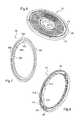
- FIG. 7is a perspective view of the cover of the pumping ring.
- FIG. 8is a perspective view of the gas pumping ring.
- vacuum chamberswere used for chemical vapour deposition with electrical heating elements, a reactive gas inlet and a purging gas supply.
- the powder-like materialsmay be from reactive gases which are capable of carrying such materials, or from a reaction between reactive gases, condensation of reactive gases, etc.
- the Applicantrealised that it was important to promote the regularity of gas flow lines in the chamber in order to obtain a deposit having a homogeneous thickness over the entire surface of the substrate.
- the heating element using a heat-exchange fluidprevents occurrences of electrical interference during the generation of a plasma by the upper wall being placed under voltage at a selected frequency.
- the heating elementmay be provided on the upper wall or on an inserted component in order to heat the upper wall and the gas inlets.
- the devicemay comprise at least one high-frequency generator which is provided with an outlet which is connected to the upper wall.
- the earth of the high-frequency generatormay be connected to the substrate support.
- the heating elementmay be electrically inactive.
- the upper wallis insulated relative to the wafer support and the side walls of the chamber so as to be able to apply a voltage between the upper wall and the wafer support.
- the substrate supportmay comprise at least one heating element in order to heat the substrate and a conductor which can be connected to earth. It is thereby possible to control the temperature profile of the substrate support.
- the number of channels of the upper wall of the chamberis greater than 500, for example, in the order of 700 for a substrate to be treated having a diameter of 200 mm.
- the first inlet of the upper wall of the chamberis connected to a first source of gas and the second inlet is connected to a second source of gas.
- the first inlet of the upper wallmay be connected to a gas source and the second inlet may be connected to an evaporator.
- a covermay comprise a conductive body, an upper chamber wall which brings about the distribution of the gases, a heating element and insulation with respect to the substrate support.
- the insulationmay be provided in the form of a ring in contact with a chamber body.
- the heating elementis protected against RF interference.
- the protectionmay be intrinsic, for example, with thermal conduction, for example, brought about by an electrically insulating heat-exchange fluid, or radiation, for example, infrared radiation, remote bringing about decoupling, or structural, for example, an insulation housing which withstands heat and in which a resistor is provided.
- the energymay be provided by a remote electrical resistor which is only slightly subjected to RF radiation.
- the upper wallmay comprise a plurality of pins forming the first channels.
- the pinsmay be force-fitted in the upper wall. Excellent sealing is obtained.
- the gas discharge ring or pumping ringmay comprise at least a portion of electrically insulating material.
- the ringmay be constructed in one piece.
- the ringmay comprise an upper portion based on a ceramic material or coated with a ceramic material and a lower portion.
- the lower portionmay be electrically conductive.
- the lower portionmay be constructed on the basis of a light alloy.
- the gas discharge ringmay comprise at least ten openings which are in communication with the chamber and which are distributed over the circumference of the ring so that the vector range of the gas discharge rate has axial symmetry with respect to the vertical axis of the chamber and the flow of the gases is of a laminar type in the envisaged flow range.
- the gas discharge ring, the upper wall of the chamber and the heating elementmay be parallel.
- the devicemay comprise an insulation component between the upper wall and a chamber body.
- the treatment devicewhich is generally designated 1 comprises a body 2 which defines a recess in a face and a cover 3 which closes the recess at that face in order to form a chamber 4 .
- a support 5which is provided with an upper surface 5 a which is intended to support a substrate to be treated, for example, by deposition.
- the support 5may comprise a base 6 and a plate 7 .
- the base 6may project through an opening 2 a of the body 2 at the side opposite the cover 3 .
- the base 6may extend away from the plate 7 (in a manner not illustrated) and may be provided with means for movement, in terms of rotation and/or translation.
- the support 5is composed of an insulating material which contains an electrode, for example, based on AlN as the insulation and Mo for the electrode.
- the support 5may be provided with a thermal control member 55 , for example, of the type described in document EP0619381, to which the reader may wish to refer.
- the member 55may be heating and/or cooling.
- the cover 3comprises a plurality of elements of generally circular form.
- the elements of the cover 3may be arranged so as to be substantially parallel with each other.
- the cover 3may carry out functions involving sealing, introducing a plurality of gases, heating the gases and the electrode in order to be able to generate an electrical field in the chamber 4 .
- the cover 3comprises a lower portion 9 and a main portion 10 .
- the cover 3rests on an upper edge of the body 2 . More specifically, the lower portion 9 of the cover 3 is generally in the form of a flat disk resting on an upper surface of the main portion 8 , forming the upper portion of the body 2 .
- the main portion 8may be constructed based on a light alloy.
- the lower portion 9 of the cover 3may be constructed based on a light alloy, for example, the same alloy.
- the generally circular main portion 10rests on the lower portion 9 .
- the main portion 10may be constructed from a light alloy.
- the main portion 10is thermally conductive and is perforated with a central hole which forms a first inlet 11 for a first gas and an oblique hole which is provided near an outer edge of the main portion 10 and which forms a second inlet 12 for a second gas.
- the main portion 10comprises a circular concavity 13 which is provided from the main surface thereof opposite the chamber 4 .
- a heating element 14is arranged in the recess 13 and comprises a lower portion 15 which is provided at the bottom of the recess 13 and an upper portion 16 .
- the lower portion 15 and the upper portion 16can be fixed together by screws 17 .
- the lower portion 15 and upper portion 16are in the form of a disk having a central hole.
- a projection 10 a of the main portion 10projects from the bottom of the recess 13 in the direction away from the chamber 4 , extending in the central hole of the lower portion 15 and upper portion 16 .
- the projection 10 ais recessed relative to the upper surface of the upper portion 16 .
- the inlet 11 for the first gasis arranged in the central projection 10 a.
- an electrically and thermally insulating washer 18for example, of a ceramic material, between the main portion 10 and the elements provided upstream in the direction of flow of the first gas.
- a connector 19brings about the connection between the washer 18 and a conduit 20 for supplying the first gas.
- the connector 19can be screwed to the washer 18 .
- Sealing jointsfor example, circular joints, may be provided between the washer 18 and the projection 10 a , on the one hand, and between the connector 19 and the washer 18 on the other.
- the lower portion 15 of the heating element 14has a helical channel 21 which has a substantially rectangular cross-section and which is formed over a plurality of turns between an end having a small diameter and an end having a large diameter.
- the channel 21allows a heat-exchange fluid to flow at a temperature, for example, between 50° and 300°.
- the heat-exchange fluidmay comprise a silicone oil or a perfluorinated compound.
- the turns of the helical channel 21are separated by a helical wall 22 which has a radial thickness less than the radial dimension of the channel 21 .
- the upper plate 16is provided with an inlet and an outlet for heat-exchange fluid (not illustrated) which are connected at the ends.
- the lower portion 15may be constructed from a thermally conductive material, for example, based on aluminium or copper.
- the upper portion 16may be constructed from a material having a level of thermal conductivity less than that of the material of the lower portion 15 , for example, a stainless steel, in particular of the type 316L.
- Two annular grooves, one 23 having a small diameter and one 24 having a large diameter,are provided in the lower portion 15 and are open at the same side as the helical channel 21 . Sealing joints may be provided in the annular grooves 23 and 24 , radially surrounding the helical channel 21 . Excellent sealing of the channel 21 which is closed by the upper portion 16 is thereby ensured.
- Screws 25are provided to fix the upper portion 16 of the heating element 14 to the main portion 10 of the cover 3 , see FIG. 2 .
- the lower portion 15is thereby secured between the bottom of the concavity 13 and the upper portion 16 , ensuring the sealing of the helical channel 21 between the lower portion 15 and the upper portion 16 of the heating element 14 .
- a concavity 26which is centred relative to the axis of the cover 3 and which is in fluid communication with the inlet 11 of the first gas.
- annular groove 27is further provided in the main portion 10 of the cover 3 from the surface opposite the heating element 14 .
- the annular groove 27is in fluid communication with the inlet 12 for the second gas.
- the annular groove 27is separated from the central concavity 26 by an annular flange 28 which is part of the main portion 10 , the central concavity 26 thereby being surrounded by the flange 28 and the groove 27 .
- the cover 3also comprises an insulating ring 29 which is provided near the outer edge of the main portion 10 .
- the ring 29is electrically insulating, in particular with respect to the lower portion 9 of the cover 3 .
- the insulating ring 29has an L-like cross-section with an upper surface and a hole in contact with the main portion 10 of the cover 3 , an outer surface having a large diameter in contact with the lower portion 9 of the cover 3 .
- the holeis also in contact with an upper wall 30 of the chamber 4 described below.
- the insulating ring 29has an annular lower wall which is in contact with a gas discharge ring 31 described below.
- the main portion 10 and the insulating ring 29 of the cover 3may be fixed to the lower portion 9 by screws 32 .
- the body 2is separated from the main portion 10 and the wall 30 by the insulating ring 29 .
- the insulating ring 29may be based on a ceramic material of the type Al 2 O 3 .
- the upper wall 30is held between a lower surface of the main portion 10 of the cover 3 and the gas discharge ring 49 .
- the upper wall 30is visible in greater detail in FIGS. 3 to 5 and is of generally annular shape.
- the upper wall 30comprises a body 31 which comprises an outer edge 32 and a central plate 33 having a thickness less than that of the outer edge 32 . Holes 34 are provided in the outer edge 32 , in particular in order to be fixed by screws which are not illustrated to the main portion 10 of the cover 3 .
- the body 31is in one piece.
- the body 31comprises a light alloy which is thermally conductive.
- a concavity 35is formed at the side opposite the chamber 4 .
- Holes 36have a substantially constant cross-section.
- Holes 37have a portion 37 a having a small diameter in the region of the concavity 35 and a widened frustoconical portion 37 b which is opposite the concavity 35 and which has a diameter which increases in the direction moving away from the concavity 35 .
- the holes 36 and the holes 37alternate, for example, being provided in the manner of a draughts-board, in a square or zigzag manner. There may be a large number of holes 36 and 37 , for example, between 500 and 1500.
- the diameter of the holes 36is greater than the diameter of the holes 37 .
- the upper wall 30also comprises a counter-plate 38 which comprises an outer edge 39 and a central portion 40 .
- the central portion 40has a thickness less than the outer edge 39 , thereby providing a concavity 41 which is orientated at the side of the central plate 33 .
- the outer edge 39 of the counter-plate 38is adjusted in the concavity 35 of the body 31 , thereby forming a distribution chamber 42 between the central plate 33 and the counter-plate 38 .
- the central portion 40 of the counter-plate 38is perforated by a plurality of through-holes 43 which are aligned with the holes 36 of the plate 33 . However, the central portion 40 is solid facing the holes 37 of the plate 33 .
- the upper wall 30comprises a plurality of pins 44 having an axial length substantially equal to the thickness of the body 31 .
- Each pin 44is mounted in a hole 36 of the central plate 33 and in a hole 43 of the central portion 40 .
- Each hole 36 and each hole 43is provided with a pin 44 . Otherwise, any remaining hole 36 or hole 43 may be provided with a plug which is not illustrated.
- the pin 44is in the form of a solid component which is provided with an outer cylindrical surface generated by revolution, an upper surface which is substantially aligned with the upper surface of the body 31 and a through-hole 45 .
- the pin 44is force-fitted in the hole 36 and in the hole 43 , for example, by fixing.
- the fittingcan be carried out using a press.
- the pin 43may be provided with a slight chamfer at the lower end thereof in the region of the outer surface thereof.
- the pin 44is brazed to the plate 33 and the counter-plate 38 .
- assembly by clamped fittingis preferred in order to conserve the geometrical dimensions of the body 31 and the counter-plate 38 .
- Clamped fittingensures excellent sealing.
- the through-hole 45places, in fluid communication, the chamber 26 which is provided at the lower face of the main portion 10 of the cover 3 and the chamber 4 , with sealing being maintained relative to the chamber 42 .
- the pin 44may be a solid component which is constructed from a metal alloy, for example, based on a light alloy, which is thermally conductive.
- the hole 45comprises a cylindrical portion 45 a which has a small diameter and which extends over the majority of the length of the pin 44 from the upper surface of the body 31 which opens in the chamber 26 , and a frustoconical portion 45 b which opens in the chamber 4 .
- the cylindrical portion 45 a of the hole 45may have a diameter which is substantially equal to the diameter of the cylindrical portion 37 a of the hole 37 which is provided in the central plate 33 of the body 31 . In this instance, the term “substantially equal” is intended to be understood to be equal to within 10%, preferably to within 5%.
- the frustoconical portion 45 b of the hole 45may have dimensions which are substantially equal to those of the frustoconical portion 37 b of the hole 37 .
- the upper wall 30comprises a plurality of holes 45 which form first communication channels between the inlet 11 for the first gas and the chamber 4 by means of the chamber 26 .
- the chamber 26brings about distribution of the flow of the first gas in the holes 45 .
- the chamber 42is provided with an inlet 46 , in the region of the groove 27 , in the form of a through-hole through the central portion 40 of the upper counter-plate 38 near the edge 39 .
- the groove 27there are provided two annular grooves 47 extending from the upper surface of the counter-plate 38 in order to receive therein two sealing joints 48 .
- the sealing joints 48are in contact with the lower surface of the main portion 10 of the cover 3 .
- the hole 46opens in the annular groove 27 which is provided from the lower surface of the main portion 10 of the cover 3 around the chamber 26 , the groove 27 being in fluid communication with the inlet 12 for the second gas.
- FIG. 4shows a single hole 46 .
- a plurality of holes 46can be constructed through the central portion 40 .
- the second gaspasses through the hole(s) 46 and becomes dispersed in the chamber 42 .
- the second gasthen passes into the holes 37 which are constructed in the central plate 33 and is introduced into the treatment chamber 4 . It is thereby possible to keep the first gas and second gas separate upstream of the chamber 4 in the direction of flow of the first and second gases. A chemical reaction is thereby prevented between some constituents of the first and second gases which may be detrimental to the step of treating the substrate or the treatment devices 1 , in particular owing to clogging.
- the heating element 14allows the first and second gases, particularly at the inlets 11 and 12 into the chamber 26 and the groove 27 , to be kept at a temperature sufficient to prevent condensation phenomena.
- the upper counter-plate 38 of the upper wall 30can be constructed from a material which conducts heat well, for example, based on a light aluminium alloy, which also allows the counter-plate 38 to be maintained at a high temperature, owing to contact with the main portion 10 of the cover 3 and thermal conduction.
- the lower portion of the body 31may also be constructed from a material having good thermal conduction, which allows the chamber 42 to be kept at a high temperature.
- the gas discharge ring 49is mounted on an annular surface 8 a of the body 8 so as to be substantially parallel with the cover 3 and in a circular axial surface 8 b forming a hole.
- the gas discharge ring 49is also in contact with the insulating ring 29 and a lower surface of the body 31 of the upper wall 30 .
- the gas discharge ringcan be constructed in one piece or in several pieces.
- the ring 49is arranged axially between the upper wall 30 and the support 5 .
- the ring 49comprises an upper portion 50 which is illustrated in FIG. 7 and a lower portion 51 which is illustrated in FIG. 8 .
- the upper portion 50is in the form of an annular component which comprises a lower planar surface 50 a , an upper surface 50 b which has a large diameter and is in contact with the insulating ring 29 , and an upper surface 50 c which has a small diameter and is in contact with the upper wall 30 , the axial thickness of the upper portion 50 being greater in the region of the upper surface 50 b having a large diameter than in the region of the upper surface 50 c having a small diameter.
- a short axial surface 50 d and a frustoconical surface 50 econnect the surfaces 50 b and 50 c .
- the upper portion 50also comprises an axial outer surface 50 f in contact with the hole 8 b of the body 8 and an internal surface 50 g having a small axial dimension.
- the upper portion 50can be constructed based on a ceramic material, of the Al 2 O 3 type or a light alloy coated with ceramic material, of the type involving aluminium with a coating of the Al 2 O 3 type.
- the upper portion 50acts as a spacer between the insulating ring 29 and the lower portion 51 and as insulation between the main portion 10 of the cover 3 and the lower portion 51 of the ring 49 .
- the lower portion 51is of generally annular form having an H-shaped cross-section.
- the lower portion 51comprises an outer wall 51 a , an inner wall 51 b and a generally radial connecting wall 51 c .
- the inner wall 51 bhas a plurality of notches 51 d which place in communication the chamber 4 , at the inner side of the inner wall 51 b , and a generally annular channel 52 which is formed between the outer wall 51 a , inner wall 51 b , connecting wall 51 c and the lower surface 50 a of the upper portion 50 .
- the notches 51 dare regularly distributed circumferentially in order to allow discharge with gas intake which is sufficiently homogeneous, with axial symmetry and a laminar flow in the envisaged flow range.
- gasesare introduced via the holes 37 , 45 of the upper wall 30 , the holes being provided substantially at the centre of the chamber 4 and the gases are discharged via the notches 51 d which are provided at the periphery of the chamber 4 , which allows the fluid flow lines in the chamber 4 to be regulated.
- the connecting wall 51 cis perforated by a plurality of communication holes 53 .
- the connecting wall 51 cis provided substantially at half of the height of the outer wall 51 a and inner wall 51 b .
- a lower channel 54is formed between the inner wall 51 a and outer wall 51 b , the connecting wall 51 c and the annular surface 8 a of the body 8 .
- the holes 53place the upper channel 52 and lower channel 54 in communication.
- the lower channel 54is in communication with a gas discharge outlet 59 which is provided in the body 8 , see FIG. 2 .
- a hole 57(see FIG. 1 ) is provided in the body 8 and in a boss 60 of substantially rectangular form projecting into the channel 52 from the connecting wall 51 c (see FIG.
- the hole 57is closed at the outlet of the body 8 (not visible in FIG. 1 ) by anti-UV treated glass in order to ensure the sealing of the chamber 4 in this regard.
- An opening 58is provided in the body 8 in order to allow the substrate to be moved to the centre of the chamber 4 on the support 5 via a vacuum transfer chamber, which may optionally be provided with a robot not illustrated in the Figures. That opening is constructed in such a manner that it does not impair the positioning of the gas discharge ring 49 .
- the upper portion 50 of the gas discharge ring 49is constructed from an electrically insulating material.
- the main portion 10 of the cover 3 , the heating element 14 and the upper wall 30 of the chamber 4are thereby electrically insulated with respect to the other elements of the treatment device 1 by the insulating washer 18 , the insulating ring 29 and the upper portion 50 of the gas discharge ring. It is thereby possible to apply a selected voltage to the main portion 10 and the upper wall 30 , for example, an alternating-current voltage at high frequency, whilst the support 5 is earthed.
- the application of a high voltageallows polarisation promoting the production of a plasma in the chamber 4 .
- the electrical connection between the cover 3 and a high-voltage supply via an impedance matching devicemay be carried out by a metal braid, for example, of copper, fixed by one of the screws 32 .
- the treatment devicecan thereby use temperatures suitable for the gases used for new generations of devices constructed on substrates, in particular vaporised solutions of solid precursors, or gases having a specific tendency towards condensation or the deposit of solid residues.
- the heating element 14 involving a heat-exchange fluid flowing in the channel 21which is inactive from an electrical point of view, is compatible with an electric voltage being applied to the cover 3 .
- the heating element 14allows the main portion 10 of the cover 3 to be kept at a temperature higher than the highest condensation temperature 1 a of the gases introduced into the chamber 4 , which allows a reduction in the risk of condensation or deposition.
- the application of an electric voltagemay be used to generate a plasma which activates the chemical deposition reaction and may also serve to carry out cleaning in situ of the walls of the chamber. Occurrences of interference between the electrical supply and the heating element 14 are prevented by heating with heat-exchange fluid.
- the deposition temperaturemay be controlled by the heating member 55 which is mounted in the plate 7 of the support 5 .
- the heating member 55allows the substrate to be kept at a selected temperature, and also the gases in the chamber 4 to be kept at a selected temperature. It is possible to introduce at least two reactive gases, one per inlet, into the chamber simultaneously.
Landscapes
- Chemical & Material Sciences (AREA)
- Engineering & Computer Science (AREA)
- General Chemical & Material Sciences (AREA)
- Chemical Kinetics & Catalysis (AREA)
- Materials Engineering (AREA)
- Mechanical Engineering (AREA)
- Metallurgy (AREA)
- Organic Chemistry (AREA)
- Physics & Mathematics (AREA)
- Condensed Matter Physics & Semiconductors (AREA)
- General Physics & Mathematics (AREA)
- Manufacturing & Machinery (AREA)
- Computer Hardware Design (AREA)
- Microelectronics & Electronic Packaging (AREA)
- Power Engineering (AREA)
- Chemical Vapour Deposition (AREA)
Abstract
Description
- The invention relates to the field of production of integrated circuits or microsystems and, more particularly, equipment for chemical vapour deposition.
- Integrated circuits or microsystems are produced from wafers or substrates which are generally composed of silicon or another semiconductor material and which are subjected to a succession of steps for depositing thin layers of various materials, masking and lithography of those layers then engraving of those layers. Between those steps for producing active elements of the devices there are interposed steps for cleaning the surfaces and inspection steps, in which the quality of the production methods is examined.
- The present invention particularly relates to equipment for depositing layers which constitute integrated circuits and microsystems and, more particularly, equipment for chemical vapour deposition.
- Various types of deposition are used in the technologies for producing integrated circuits and microsystems: so-called physical depositions (atomisation, evaporation) and so-called chemical depositions: chemical vapour deposition, atomic layer deposition, electrochemical deposition, to set out merely the main categories which are themselves subdivided into a plurality of sub-categories.
- Physical depositions which more particularly involve the deposit of metal layers are carried out in pressure ranges of from a few nanobar to a few microbar. They have the advantage of being relatively simple to carry out because they use only neutral gases in order to carry out the depositions. Owing to their directional nature, however, they have the disadvantage of not uniformly covering patterns which have horizontal surfaces and vertical or quasi-vertical surfaces, such as the ones which appear in the production of integrated circuits and microsystems.
- The rate of coverage of a surface by a physical deposit is directly proportional to the solid angle when viewed from that surface. As a result, the projecting portions and the horizontal surfaces of a pattern are covered with a thickness greater than the reflex angles or the vertical surfaces. Therefore, there results inhomogeneity of the deposits which may impair the correct operation of the electronic device produced.
- In chemical depositions, there is brought about adsorption, chemical sorption or a heterogeneous reaction at the surface of the substrate to be covered. That adsorption, chemical sorption or reaction occurs at all the surfaces if adequate conditions involving temperature, pressure and the concentration of the reagents are combined in the case of a vapour phase deposition. As a result, the chemical depositions and particularly the chemical vapour depositions intrinsically cover in a uniform manner the surface of the patterns constituting the integrated circuits or microsystems. That characteristic is particularly advantageous in recent circuits or microsystems where the patterns to be covered may have very high form factors (relationship between the width and the height of the pattern).
- The systems for producing integrated circuits or microsystems generally comprise a treatment chamber comprising a support for the substrate in the chamber.
- A gas distribution assembly, also referred to using the term “showerhead”, provides one or more treatment gases near the substrate. The gases may be used to form a plasma. Such methods may comprise chemical vapour deposition (CVD), plasma enhanced chemical vapour deposition (PECVD) to deposit a layer on the substrate or an engraving reaction to remove material from the wafer.
- In this regard, there are known documents U.S. Pat. No. 5,292,554, U.S. Pat. No. 5,516,367, which have been adapted to old production technologies, WO03/060185 and US2006/21703.
- The Applicant became aware that known treatment chambers were liable to allow the occurrence of interference reactions between several gases upstream of the gas distribution assembly. Such interference reactions may deposit solids of powder-like form at undesirable locations. Furthermore, since the pressure upstream of the gas distribution assembly is higher than at the surface of the substrate to be covered, such interference reactions in the gas state are promoted.
- Furthermore, the Applicant identified that the most recent materials whose use is envisaged in the field of integrated circuits and microsystems may involve the risk of the holes of the gas distribution assembly becoming clogged.
- The invention is intended to improve the situation.
- The device for treating substrates comprises a chamber having controlled pressure and temperature and a substrate support. The support is provided in the chamber. The chamber comprises a plurality of gas inlets, for example, two. The device comprises a plurality of first channels which are connected to a first gas inlet and a plurality of second channels which are connected to a second gas inlet. The first and second channels open in the chamber. They are regularly distributed in the upper wall of the chamber. The device also comprises a heating element which is capable of heating the upper wall and a gas discharge ring which is provided between the upper wall and the substrate support. The upper wall is electrically conductive and insulated relative to the wafer support of the chamber so as to be able to apply a voltage between the upper wall and the wafer support.
- The invention also relates to a process for treating substrates in a chamber with controlled temperature and pressure, a substrate being supported by a support which is provided in the chamber. Gas inlets are heated to a temperature higher than a condensation temperature, it being possible to carry out the heating using a heat-exchange fluid. Gases are introduced via the inlets, the gases being introduced through an upper wall of the chamber provided under the inlets, the introduction being effected via different holes in accordance with the type of gas and extending into the chamber, the holes being regularly distributed. If it is desirable to generate a plasma, a high-frequency electrical voltage is applied to the upper wall in relation to the support.
- The chamber may form a vessel whose pressure is adjusted below atmospheric pressure by means of a pumping system, on the one hand, and a pressure control system on the other.
- The heating element, in particular involving a heat-exchange fluid, allows heating of the gases to a suitable temperature in the inlets, for example, a temperature allowing condensation phenomena to be limited, taking into account the fact that the pressure of the gases in the inlets is slightly greater than the pressure of the gases in the chamber. The heating element may be provided above or inside the upper wall.
- The heating element, in particular involving a heat-exchange fluid, also allows a voltage to be applied so as to generate a plasma, with the generation of interference being prevented, which would not be the case with heating of the electrical resistance type. Alternatively, an infrared lamp may be used to bring about the remote heating of the cover. An insulated resistor may also be used and mounted in an insulating casing, particularly composed of ceramic material.
- Furthermore, a voltage being applied between the upper wall and the support in order to generate a plasma between those two elements allows the chamber to be efficiently cleaned in situ by introducing gases which are selected to react with the deposits which may be present inside the chamber. The cleaning gases are selected so that the products of the reaction of those gases with the deposits are volatile and can thereby be discharged by pumping. The treatment device and process are very suitable for the deposit of materials for producing microelectronic and micro-electromechanical devices, such as, by way of non-limiting example: HfO2, ZrO2, Ru, Pt, Ir and Ir and IrO2, alone or in admixture. Those materials are often prepared from powdered organometallic precursors which are placed in a liquid solution in a suitable solvent, then evaporated. With such gases from solutions of solid compounds having an evaporation temperature that is different from that of the solvent, the risk of a conventional installation becoming clogged is relatively high owing to either condensation or decomposition of the solid product.
- The present invention will be better understood from a reading of the detailed description of several embodiments which are set out by way of non-limiting example and illustrated with reference to the appended drawings, in which:
FIGS. 1 and 2 are axial sections in two intersecting planes of a treatment chamber;FIG. 3 is a detailed view of the upper wall of the treatment chamber ofFIGS. 1 and 2 ;FIGS. 4 and 5 are detailed views ofFIG. 3 ;FIG. 6 is a perspective view of part of the heating element;FIG. 7 is a perspective view of the cover of the pumping ring; andFIG. 8 is a perspective view of the gas pumping ring.- In the 1990s, vacuum chambers were used for chemical vapour deposition with electrical heating elements, a reactive gas inlet and a purging gas supply.
- Subsequently, attempts were made to limit the effects of the reactive gases on the walls of the chamber by providing an anti-corrosion layer of refractory material which is resistant to chemical attack by the gases in order to conserve the reflective properties of the internal wall of the reaction chamber.
- More recently, attempts were made to introduce two reactive gases into a treatment chamber by means of a gas distribution assembly of brazed nickel.
- However, the Applicant became aware of a problem which had not currently been identified, that of clogging of the upper wall owing to deposits of powder-like materials. The powder-like materials may be from reactive gases which are capable of carrying such materials, or from a reaction between reactive gases, condensation of reactive gases, etc.
- Furthermore, the Applicant realised that it was important to promote the regularity of gas flow lines in the chamber in order to obtain a deposit having a homogeneous thickness over the entire surface of the substrate.
- For a general description of a treatment chamber, reference may be made to documents WO03/060185 and US2006/21703.
- The heating element using a heat-exchange fluid prevents occurrences of electrical interference during the generation of a plasma by the upper wall being placed under voltage at a selected frequency. The heating element may be provided on the upper wall or on an inserted component in order to heat the upper wall and the gas inlets.
- The device may comprise at least one high-frequency generator which is provided with an outlet which is connected to the upper wall. The earth of the high-frequency generator may be connected to the substrate support. The heating element may be electrically inactive. The upper wall is insulated relative to the wafer support and the side walls of the chamber so as to be able to apply a voltage between the upper wall and the wafer support.
- The substrate support may comprise at least one heating element in order to heat the substrate and a conductor which can be connected to earth. It is thereby possible to control the temperature profile of the substrate support.
- The number of channels of the upper wall of the chamber is greater than 500, for example, in the order of 700 for a substrate to be treated having a diameter of 200 mm.
- The first inlet of the upper wall of the chamber is connected to a first source of gas and the second inlet is connected to a second source of gas.
- The first inlet of the upper wall may be connected to a gas source and the second inlet may be connected to an evaporator.
- A cover may comprise a conductive body, an upper chamber wall which brings about the distribution of the gases, a heating element and insulation with respect to the substrate support. The insulation may be provided in the form of a ring in contact with a chamber body. The heating element is protected against RF interference. The protection may be intrinsic, for example, with thermal conduction, for example, brought about by an electrically insulating heat-exchange fluid, or radiation, for example, infrared radiation, remote bringing about decoupling, or structural, for example, an insulation housing which withstands heat and in which a resistor is provided. In the case of a heat-exchange fluid, the energy may be provided by a remote electrical resistor which is only slightly subjected to RF radiation.
- The upper wall may comprise a plurality of pins forming the first channels. The pins may be force-fitted in the upper wall. Excellent sealing is obtained.
- The gas discharge ring or pumping ring may comprise at least a portion of electrically insulating material. The ring may be constructed in one piece. The ring may comprise an upper portion based on a ceramic material or coated with a ceramic material and a lower portion. The lower portion may be electrically conductive. The lower portion may be constructed on the basis of a light alloy.
- The gas discharge ring may comprise at least ten openings which are in communication with the chamber and which are distributed over the circumference of the ring so that the vector range of the gas discharge rate has axial symmetry with respect to the vertical axis of the chamber and the flow of the gases is of a laminar type in the envisaged flow range. The gas discharge ring, the upper wall of the chamber and the heating element may be parallel.
- The device may comprise an insulation component between the upper wall and a chamber body.
- In the embodiment illustrated in the Figures, the treatment device which is generally designated1 comprises a
body 2 which defines a recess in a face and acover 3 which closes the recess at that face in order to form achamber 4. There is provided in the chamber4 asupport 5 which is provided with anupper surface 5awhich is intended to support a substrate to be treated, for example, by deposition. Thesupport 5 may comprise abase 6 and aplate 7. Thebase 6 may project through anopening 2aof thebody 2 at the side opposite thecover 3. Thebase 6 may extend away from the plate7 (in a manner not illustrated) and may be provided with means for movement, in terms of rotation and/or translation. Thesupport 5 is composed of an insulating material which contains an electrode, for example, based on AlN as the insulation and Mo for the electrode. Thesupport 5 may be provided with athermal control member 55, for example, of the type described in document EP0619381, to which the reader may wish to refer. Themember 55 may be heating and/or cooling. - The
cover 3 comprises a plurality of elements of generally circular form. The elements of thecover 3 may be arranged so as to be substantially parallel with each other. Thecover 3 may carry out functions involving sealing, introducing a plurality of gases, heating the gases and the electrode in order to be able to generate an electrical field in thechamber 4. Thecover 3 comprises alower portion 9 and amain portion 10. - The
cover 3 rests on an upper edge of thebody 2. More specifically, thelower portion 9 of thecover 3 is generally in the form of a flat disk resting on an upper surface of themain portion 8, forming the upper portion of thebody 2. Themain portion 8 may be constructed based on a light alloy. Thelower portion 9 of thecover 3 may be constructed based on a light alloy, for example, the same alloy. - The generally circular
main portion 10 rests on thelower portion 9. Themain portion 10 may be constructed from a light alloy. Themain portion 10 is thermally conductive and is perforated with a central hole which forms a first inlet11 for a first gas and an oblique hole which is provided near an outer edge of themain portion 10 and which forms asecond inlet 12 for a second gas. - The
main portion 10 comprises acircular concavity 13 which is provided from the main surface thereof opposite thechamber 4. Aheating element 14 is arranged in therecess 13 and comprises alower portion 15 which is provided at the bottom of therecess 13 and anupper portion 16. Thelower portion 15 and theupper portion 16 can be fixed together byscrews 17. Thelower portion 15 andupper portion 16 are in the form of a disk having a central hole. - A
projection 10aof themain portion 10 projects from the bottom of therecess 13 in the direction away from thechamber 4, extending in the central hole of thelower portion 15 andupper portion 16. Theprojection 10ais recessed relative to the upper surface of theupper portion 16. The inlet11 for the first gas is arranged in thecentral projection 10a. - There is provided, above the
central projection 10a, an electrically and thermally insulatingwasher 18, for example, of a ceramic material, between themain portion 10 and the elements provided upstream in the direction of flow of the first gas. Aconnector 19 brings about the connection between thewasher 18 and aconduit 20 for supplying the first gas. Theconnector 19 can be screwed to thewasher 18. Sealing joints, for example, circular joints, may be provided between thewasher 18 and theprojection 10a, on the one hand, and between theconnector 19 and thewasher 18 on the other. - As can be seen in greater detail in
FIG. 6 , thelower portion 15 of theheating element 14 has ahelical channel 21 which has a substantially rectangular cross-section and which is formed over a plurality of turns between an end having a small diameter and an end having a large diameter. Thechannel 21 allows a heat-exchange fluid to flow at a temperature, for example, between 50° and 300°. The heat-exchange fluid may comprise a silicone oil or a perfluorinated compound. The turns of thehelical channel 21 are separated by ahelical wall 22 which has a radial thickness less than the radial dimension of thechannel 21. Theupper plate 16 is provided with an inlet and an outlet for heat-exchange fluid (not illustrated) which are connected at the ends. Thelower portion 15 may be constructed from a thermally conductive material, for example, based on aluminium or copper. Theupper portion 16 may be constructed from a material having a level of thermal conductivity less than that of the material of thelower portion 15, for example, a stainless steel, in particular of the type 316L. - Two annular grooves, one23 having a small diameter and one24 having a large diameter, are provided in the
lower portion 15 and are open at the same side as thehelical channel 21. Sealing joints may be provided in theannular grooves helical channel 21. Excellent sealing of thechannel 21 which is closed by theupper portion 16 is thereby ensured. Screws 25 are provided to fix theupper portion 16 of theheating element 14 to themain portion 10 of thecover 3, seeFIG. 2 . Thelower portion 15 is thereby secured between the bottom of theconcavity 13 and theupper portion 16, ensuring the sealing of thehelical channel 21 between thelower portion 15 and theupper portion 16 of theheating element 14.- Starting from the surface of the
main portion 10 of thecover 3, opposite theheating element 14, there is provided aconcavity 26 which is centred relative to the axis of thecover 3 and which is in fluid communication with the inlet11 of the first gas. - An
annular groove 27 is further provided in themain portion 10 of thecover 3 from the surface opposite theheating element 14. Theannular groove 27 is in fluid communication with theinlet 12 for the second gas. Theannular groove 27 is separated from thecentral concavity 26 by anannular flange 28 which is part of themain portion 10, thecentral concavity 26 thereby being surrounded by theflange 28 and thegroove 27. - The
cover 3 also comprises an insulatingring 29 which is provided near the outer edge of themain portion 10. Thering 29 is electrically insulating, in particular with respect to thelower portion 9 of thecover 3. The insulatingring 29 has an L-like cross-section with an upper surface and a hole in contact with themain portion 10 of thecover 3, an outer surface having a large diameter in contact with thelower portion 9 of thecover 3. The hole is also in contact with anupper wall 30 of thechamber 4 described below. The insulatingring 29 has an annular lower wall which is in contact with agas discharge ring 31 described below. Themain portion 10 and the insulatingring 29 of thecover 3 may be fixed to thelower portion 9 byscrews 32. Thebody 2 is separated from themain portion 10 and thewall 30 by the insulatingring 29. The insulatingring 29 may be based on a ceramic material of the type Al2O3. - The
upper wall 30 is held between a lower surface of themain portion 10 of thecover 3 and thegas discharge ring 49. Theupper wall 30 is visible in greater detail inFIGS. 3 to 5 and is of generally annular shape. Theupper wall 30 comprises abody 31 which comprises anouter edge 32 and acentral plate 33 having a thickness less than that of theouter edge 32.Holes 34 are provided in theouter edge 32, in particular in order to be fixed by screws which are not illustrated to themain portion 10 of thecover 3. Thebody 31 is in one piece. Thebody 31 comprises a light alloy which is thermally conductive. - Owing to the difference in thickness between the
central plate 33 and theouter edge 32, aconcavity 35 is formed at the side opposite thechamber 4. There are provided in thecentral plate 33 through-holes of at least two types.Holes 36 have a substantially constant cross-section.Holes 37 have aportion 37ahaving a small diameter in the region of theconcavity 35 and a widenedfrustoconical portion 37bwhich is opposite theconcavity 35 and which has a diameter which increases in the direction moving away from theconcavity 35. Theholes 36 and theholes 37 alternate, for example, being provided in the manner of a draughts-board, in a square or zigzag manner. There may be a large number ofholes holes 36 is greater than the diameter of theholes 37. - The
upper wall 30 also comprises a counter-plate38 which comprises anouter edge 39 and acentral portion 40. Thecentral portion 40 has a thickness less than theouter edge 39, thereby providing aconcavity 41 which is orientated at the side of thecentral plate 33. Theouter edge 39 of the counter-plate38 is adjusted in theconcavity 35 of thebody 31, thereby forming adistribution chamber 42 between thecentral plate 33 and the counter-plate38. Thecentral portion 40 of the counter-plate38 is perforated by a plurality of through-holes 43 which are aligned with theholes 36 of theplate 33. However, thecentral portion 40 is solid facing theholes 37 of theplate 33. - The
upper wall 30 comprises a plurality ofpins 44 having an axial length substantially equal to the thickness of thebody 31. Eachpin 44 is mounted in ahole 36 of thecentral plate 33 and in ahole 43 of thecentral portion 40. Eachhole 36 and eachhole 43 is provided with apin 44. Otherwise, any remaininghole 36 orhole 43 may be provided with a plug which is not illustrated. Thepin 44 is in the form of a solid component which is provided with an outer cylindrical surface generated by revolution, an upper surface which is substantially aligned with the upper surface of thebody 31 and a through-hole 45. - The
pin 44 is force-fitted in thehole 36 and in thehole 43, for example, by fixing. The fitting can be carried out using a press. In order to facilitate the fixing, thepin 43 may be provided with a slight chamfer at the lower end thereof in the region of the outer surface thereof. In a variant, thepin 44 is brazed to theplate 33 and the counter-plate38. However, assembly by clamped fitting is preferred in order to conserve the geometrical dimensions of thebody 31 and the counter-plate38. Clamped fitting ensures excellent sealing. The through-hole 45 places, in fluid communication, thechamber 26 which is provided at the lower face of themain portion 10 of thecover 3 and thechamber 4, with sealing being maintained relative to thechamber 42. Thepin 44 may be a solid component which is constructed from a metal alloy, for example, based on a light alloy, which is thermally conductive. Thehole 45 comprises acylindrical portion 45awhich has a small diameter and which extends over the majority of the length of thepin 44 from the upper surface of thebody 31 which opens in thechamber 26, and afrustoconical portion 45bwhich opens in thechamber 4. Thecylindrical portion 45aof thehole 45 may have a diameter which is substantially equal to the diameter of thecylindrical portion 37aof thehole 37 which is provided in thecentral plate 33 of thebody 31. In this instance, the term “substantially equal” is intended to be understood to be equal to within 10%, preferably to within 5%. - The
frustoconical portion 45bof thehole 45 may have dimensions which are substantially equal to those of thefrustoconical portion 37bof thehole 37. - In other words, the
upper wall 30 comprises a plurality ofholes 45 which form first communication channels between the inlet11 for the first gas and thechamber 4 by means of thechamber 26. Thechamber 26 brings about distribution of the flow of the first gas in theholes 45. - As can be seen more particularly in
FIG. 4 , thechamber 42 is provided with aninlet 46, in the region of thegroove 27, in the form of a through-hole through thecentral portion 40 of theupper counter-plate 38 near theedge 39. Around thegroove 27 there are provided twoannular grooves 47 extending from the upper surface of the counter-plate38 in order to receive therein two sealingjoints 48. The sealing joints48 are in contact with the lower surface of themain portion 10 of thecover 3. Thehole 46 opens in theannular groove 27 which is provided from the lower surface of themain portion 10 of thecover 3 around thechamber 26, thegroove 27 being in fluid communication with theinlet 12 for the second gas.FIG. 4 shows asingle hole 46. - In order to promote the most homogeneous possible flow of the second gas, flowing from the
inlet 12 into thegroove 27, a plurality ofholes 46 can be constructed through thecentral portion 40. The second gas passes through the hole(s)46 and becomes dispersed in thechamber 42. The second gas then passes into theholes 37 which are constructed in thecentral plate 33 and is introduced into thetreatment chamber 4. It is thereby possible to keep the first gas and second gas separate upstream of thechamber 4 in the direction of flow of the first and second gases. A chemical reaction is thereby prevented between some constituents of the first and second gases which may be detrimental to the step of treating the substrate or thetreatment devices 1, in particular owing to clogging. - The
heating element 14 allows the first and second gases, particularly at theinlets 11 and12 into thechamber 26 and thegroove 27, to be kept at a temperature sufficient to prevent condensation phenomena. Furthermore, theupper counter-plate 38 of theupper wall 30 can be constructed from a material which conducts heat well, for example, based on a light aluminium alloy, which also allows the counter-plate38 to be maintained at a high temperature, owing to contact with themain portion 10 of thecover 3 and thermal conduction. The lower portion of thebody 31 may also be constructed from a material having good thermal conduction, which allows thechamber 42 to be kept at a high temperature. - The
gas discharge ring 49 is mounted on anannular surface 8aof thebody 8 so as to be substantially parallel with thecover 3 and in a circularaxial surface 8bforming a hole. Thegas discharge ring 49 is also in contact with the insulatingring 29 and a lower surface of thebody 31 of theupper wall 30. The gas discharge ring can be constructed in one piece or in several pieces. Thering 49 is arranged axially between theupper wall 30 and thesupport 5. - In the embodiment illustrated, the
ring 49 comprises anupper portion 50 which is illustrated inFIG. 7 and alower portion 51 which is illustrated inFIG. 8 . Theupper portion 50 is in the form of an annular component which comprises a lowerplanar surface 50a, anupper surface 50bwhich has a large diameter and is in contact with the insulatingring 29, and anupper surface 50cwhich has a small diameter and is in contact with theupper wall 30, the axial thickness of theupper portion 50 being greater in the region of theupper surface 50bhaving a large diameter than in the region of theupper surface 50chaving a small diameter. A shortaxial surface 50dand afrustoconical surface 50econnect thesurfaces upper portion 50 also comprises an axialouter surface 50fin contact with thehole 8bof thebody 8 and aninternal surface 50ghaving a small axial dimension. Theupper portion 50 can be constructed based on a ceramic material, of the Al2O3type or a light alloy coated with ceramic material, of the type involving aluminium with a coating of the Al2O3type. Theupper portion 50 acts as a spacer between the insulatingring 29 and thelower portion 51 and as insulation between themain portion 10 of thecover 3 and thelower portion 51 of thering 49. - The
lower portion 51 is of generally annular form having an H-shaped cross-section. Thelower portion 51 comprises anouter wall 51a, aninner wall 51band a generally radial connectingwall 51c. Theinner wall 51bhas a plurality ofnotches 51dwhich place in communication thechamber 4, at the inner side of theinner wall 51b, and a generallyannular channel 52 which is formed between theouter wall 51a,inner wall 51b, connectingwall 51cand thelower surface 50aof theupper portion 50. Thenotches 51dare regularly distributed circumferentially in order to allow discharge with gas intake which is sufficiently homogeneous, with axial symmetry and a laminar flow in the envisaged flow range. In that manner, gases are introduced via theholes upper wall 30, the holes being provided substantially at the centre of thechamber 4 and the gases are discharged via thenotches 51dwhich are provided at the periphery of thechamber 4, which allows the fluid flow lines in thechamber 4 to be regulated. - The connecting
wall 51cis perforated by a plurality of communication holes53. The connectingwall 51cis provided substantially at half of the height of theouter wall 51aandinner wall 51b. Alower channel 54 is formed between theinner wall 51aandouter wall 51b, the connectingwall 51cand theannular surface 8aof thebody 8. Theholes 53 place theupper channel 52 andlower channel 54 in communication. Thelower channel 54 is in communication with agas discharge outlet 59 which is provided in thebody 8, seeFIG. 2 . Furthermore, a hole57 (seeFIG. 1 ) is provided in thebody 8 and in aboss 60 of substantially rectangular form projecting into thechannel 52 from the connectingwall 51c(seeFIG. 8 ) in order to allow viewing of the interior of the chamber when a plasma is produced in thechamber 4, for example, using an optical emission spectrometer. Thehole 57 is closed at the outlet of the body8 (not visible inFIG. 1 ) by anti-UV treated glass in order to ensure the sealing of thechamber 4 in this regard. Anopening 58 is provided in thebody 8 in order to allow the substrate to be moved to the centre of thechamber 4 on thesupport 5 via a vacuum transfer chamber, which may optionally be provided with a robot not illustrated in the Figures. That opening is constructed in such a manner that it does not impair the positioning of thegas discharge ring 49. - In one embodiment, the
upper portion 50 of thegas discharge ring 49 is constructed from an electrically insulating material. Themain portion 10 of thecover 3, theheating element 14 and theupper wall 30 of thechamber 4 are thereby electrically insulated with respect to the other elements of thetreatment device 1 by the insulatingwasher 18, the insulatingring 29 and theupper portion 50 of the gas discharge ring. It is thereby possible to apply a selected voltage to themain portion 10 and theupper wall 30, for example, an alternating-current voltage at high frequency, whilst thesupport 5 is earthed. - The application of a high voltage allows polarisation promoting the production of a plasma in the
chamber 4. The electrical connection between thecover 3 and a high-voltage supply via an impedance matching device may be carried out by a metal braid, for example, of copper, fixed by one of thescrews 32. - The treatment device can thereby use temperatures suitable for the gases used for new generations of devices constructed on substrates, in particular vaporised solutions of solid precursors, or gases having a specific tendency towards condensation or the deposit of solid residues.
- The
heating element 14 involving a heat-exchange fluid flowing in thechannel 21, which is inactive from an electrical point of view, is compatible with an electric voltage being applied to thecover 3. Theheating element 14 allows themain portion 10 of thecover 3 to be kept at a temperature higher than the highest condensation temperature1aof the gases introduced into thechamber 4, which allows a reduction in the risk of condensation or deposition. The application of an electric voltage may be used to generate a plasma which activates the chemical deposition reaction and may also serve to carry out cleaning in situ of the walls of the chamber. Occurrences of interference between the electrical supply and theheating element 14 are prevented by heating with heat-exchange fluid. Furthermore, the deposition temperature may be controlled by theheating member 55 which is mounted in theplate 7 of thesupport 5. Theheating member 55 allows the substrate to be kept at a selected temperature, and also the gases in thechamber 4 to be kept at a selected temperature. It is possible to introduce at least two reactive gases, one per inlet, into the chamber simultaneously.
Claims (16)
Applications Claiming Priority (3)
| Application Number | Priority Date | Filing Date | Title |
|---|---|---|---|
| FR0802375AFR2930561B1 (en) | 2008-04-28 | 2008-04-28 | DEVICE AND METHOD FOR CHEMICAL TREATMENT IN STEAM PHASE. |
| FR0802375 | 2008-04-28 | ||
| PCT/FR2009/000479WO2009136019A2 (en) | 2008-04-28 | 2009-04-22 | Device and process for chemical vapor phase treatment |
Publications (2)
| Publication Number | Publication Date |
|---|---|
| US20110143551A1true US20110143551A1 (en) | 2011-06-16 |
| US8967081B2 US8967081B2 (en) | 2015-03-03 |
Family
ID=40303474
Family Applications (1)
| Application Number | Title | Priority Date | Filing Date |
|---|---|---|---|
| US12/990,143ActiveUS8967081B2 (en) | 2008-04-28 | 2009-04-22 | Device and process for chemical vapor phase treatment |
Country Status (5)
| Country | Link |
|---|---|
| US (1) | US8967081B2 (en) |
| EP (1) | EP2271790B1 (en) |
| KR (1) | KR101639690B1 (en) |
| FR (1) | FR2930561B1 (en) |
| WO (1) | WO2009136019A2 (en) |
Cited By (9)
| Publication number | Priority date | Publication date | Assignee | Title |
|---|---|---|---|---|
| CN105088334A (en)* | 2014-04-28 | 2015-11-25 | 北京北方微电子基地设备工艺研究中心有限责任公司 | Top cover apparatus and technology equipment |
| US20150361582A1 (en)* | 2014-06-17 | 2015-12-17 | Veeco Instruments, Inc. | Gas Flow Flange For A Rotating Disk Reactor For Chemical Vapor Deposition |
| CN105431924A (en)* | 2014-04-09 | 2016-03-23 | 应用材料公司 | Symmetric chamber body design architecture to address variable process volumes with improved flow uniformity/gas conductance |
| WO2019227861A1 (en)* | 2018-06-01 | 2019-12-05 | 北京北方华创微电子装备有限公司 | Upper electrode assembly, reaction chamber and atomic layer deposition device |
| CN112176318A (en)* | 2019-07-03 | 2021-01-05 | Asm Ip私人控股有限公司 | Temperature control assembly for substrate processing apparatus and method of use |
| US11193207B2 (en)* | 2017-01-16 | 2021-12-07 | Kobus Sas | Treatment chamber for a chemical vapour deposition (CVD) reactor and thermalization process carried out in this chamber |
| CN114464519A (en)* | 2021-12-27 | 2022-05-10 | 拓荆科技股份有限公司 | Gas extraction ring and semiconductor processing device |
| US20230073150A1 (en)* | 2021-09-09 | 2023-03-09 | Applied Materials, Inc. | Heated lid for a process chamber |
| WO2024097853A1 (en)* | 2022-11-03 | 2024-05-10 | Lam Research Corporation | Segregated reactant delivery using showerhead and shroud |
Families Citing this family (17)
| Publication number | Priority date | Publication date | Assignee | Title |
|---|---|---|---|---|
| US9267742B2 (en)* | 2010-01-27 | 2016-02-23 | Applied Materials, Inc. | Apparatus for controlling the temperature uniformity of a substrate |
| US9441295B2 (en)* | 2010-05-14 | 2016-09-13 | Solarcity Corporation | Multi-channel gas-delivery system |
| KR101295794B1 (en)* | 2011-05-31 | 2013-08-09 | 세메스 주식회사 | Apparatus for treating substrate |
| DE102012215513A1 (en)* | 2012-08-31 | 2014-03-06 | J. Schmalz Gmbh | gripping device |
| FR3002242B1 (en)* | 2013-02-21 | 2015-04-03 | Altatech Semiconductor | CHEMICAL VAPOR DEPOSITION DEVICE |
| FR3002241B1 (en) | 2013-02-21 | 2015-11-20 | Altatech Semiconductor | CHEMICAL VAPOR DEPOSITION DEVICE |
| US20160359080A1 (en) | 2015-06-07 | 2016-12-08 | Solarcity Corporation | System, method and apparatus for chemical vapor deposition |
| USD810705S1 (en)* | 2016-04-01 | 2018-02-20 | Veeco Instruments Inc. | Self-centering wafer carrier for chemical vapor deposition |
| US10325790B2 (en)* | 2016-04-29 | 2019-06-18 | Applied Materials, Inc. | Methods and apparatus for correcting substrate deformity |
| US9748434B1 (en) | 2016-05-24 | 2017-08-29 | Tesla, Inc. | Systems, method and apparatus for curing conductive paste |
| US9954136B2 (en) | 2016-08-03 | 2018-04-24 | Tesla, Inc. | Cassette optimized for an inline annealing system |
| FR3056993B1 (en) | 2016-10-04 | 2018-10-12 | Kobus Sas | DEVICE FOR SUPPLYING GAS TO A GAS PHASE CHEMICAL DEPOSITION REACTOR |
| FR3056992B1 (en) | 2016-10-04 | 2022-03-11 | Unity Semiconductor | METHOD FOR INJECTION OF CHEMICAL SPECIES IN GASEOUS PHASE IN PULSED FORM WITH PLASMA |
| US10115856B2 (en) | 2016-10-31 | 2018-10-30 | Tesla, Inc. | System and method for curing conductive paste using induction heating |
| FR3070399B1 (en) | 2017-08-29 | 2020-09-25 | Kobus Sas | PROCESS FOR THE DEPOSIT OF AN INSULATING MATERIAL IN A VIA, PULSE CVD REACTOR IMPLEMENTING THIS PROCESS |
| KR102251770B1 (en)* | 2018-01-24 | 2021-05-12 | 어플라이드 머티어리얼스, 인코포레이티드 | High temperature faceplate with hybrid material design |
| US11970775B2 (en)* | 2018-08-10 | 2024-04-30 | Applied Materials, Inc. | Showerhead for providing multiple materials to a process chamber |
Citations (86)
| Publication number | Priority date | Publication date | Assignee | Title |
|---|---|---|---|---|
| US4100879A (en)* | 1977-02-08 | 1978-07-18 | Grigory Borisovich Goldin | Device for epitaxial growing of semiconductor periodic structures from gas phase |
| US4612077A (en)* | 1985-07-29 | 1986-09-16 | The Perkin-Elmer Corporation | Electrode for plasma etching system |
| US5052339A (en)* | 1990-10-16 | 1991-10-01 | Air Products And Chemicals, Inc. | Radio frequency plasma enhanced chemical vapor deposition process and reactor |
| US5366585A (en)* | 1993-01-28 | 1994-11-22 | Applied Materials, Inc. | Method and apparatus for protection of conductive surfaces in a plasma processing reactor |
| US5423918A (en)* | 1993-09-21 | 1995-06-13 | Applied Materials, Inc. | Method for reducing particulate contamination during plasma processing of semiconductor devices |
| US5720818A (en)* | 1996-04-26 | 1998-02-24 | Applied Materials, Inc. | Conduits for flow of heat transfer fluid to the surface of an electrostatic chuck |
| US5838121A (en)* | 1996-11-18 | 1998-11-17 | Applied Materials, Inc. | Dual blade robot |
| US5844195A (en)* | 1996-11-18 | 1998-12-01 | Applied Materials, Inc. | Remote plasma source |
| US5855681A (en)* | 1996-11-18 | 1999-01-05 | Applied Materials, Inc. | Ultra high throughput wafer vacuum processing system |
| US5871586A (en)* | 1994-06-14 | 1999-02-16 | T. Swan & Co. Limited | Chemical vapor deposition |
| US5884009A (en)* | 1997-08-07 | 1999-03-16 | Tokyo Electron Limited | Substrate treatment system |
| US5902088A (en)* | 1996-11-18 | 1999-05-11 | Applied Materials, Inc. | Single loadlock chamber with wafer cooling function |
| US5905302A (en)* | 1996-11-18 | 1999-05-18 | Applied Materials, Inc. | Loadlock cassette with wafer support rails |
| US5904799A (en)* | 1993-04-16 | 1999-05-18 | Micron Technology, Inc. | Method and apparatus for improving etch uniformity in remote source plasma reactors with powered wafer chucks |
| US5909994A (en)* | 1996-11-18 | 1999-06-08 | Applied Materials, Inc. | Vertical dual loadlock chamber |
| US5911834A (en)* | 1996-11-18 | 1999-06-15 | Applied Materials, Inc. | Gas delivery system |
| US5933314A (en)* | 1997-06-27 | 1999-08-03 | Lam Research Corp. | Method and an apparatus for offsetting plasma bias voltage in bi-polar electro-static chucks |
| US5935337A (en)* | 1995-04-20 | 1999-08-10 | Ebara Corporation | Thin-film vapor deposition apparatus |
| US5948224A (en)* | 1992-03-24 | 1999-09-07 | Balzers Aktiengsellschaft | Method of controlling a treatment process and vacuum treatment apparatus |
| US5950925A (en)* | 1996-10-11 | 1999-09-14 | Ebara Corporation | Reactant gas ejector head |
| US6022446A (en)* | 1995-08-21 | 2000-02-08 | Shan; Hongching | Shallow magnetic fields for generating circulating electrons to enhance plasma processing |
| US6024044A (en)* | 1997-10-09 | 2000-02-15 | Applied Komatsu Technology, Inc. | Dual frequency excitation of plasma for film deposition |
| US6077157A (en)* | 1996-11-18 | 2000-06-20 | Applied Materials, Inc. | Process chamber exhaust system |
| US6082950A (en)* | 1996-11-18 | 2000-07-04 | Applied Materials, Inc. | Front end wafer staging with wafer cassette turntables and on-the-fly wafer center finding |
| US6101969A (en)* | 1992-11-12 | 2000-08-15 | Ngk Insulators, Ltd. | Plasma-generating electrode device, an electrode-embedded article, and a method of manufacturing thereof |
| US6132512A (en)* | 1997-01-08 | 2000-10-17 | Ebara Corporation | Vapor-phase film growth apparatus and gas ejection head |
| US6152070A (en)* | 1996-11-18 | 2000-11-28 | Applied Materials, Inc. | Tandem process chamber |
| US6203620B1 (en)* | 1996-07-10 | 2001-03-20 | Cvc Products Inc | Hermetically-sealed inductively-coupled plasma source structure and method of use |
| US6224312B1 (en)* | 1996-11-18 | 2001-05-01 | Applied Materials, Inc. | Optimal trajectory robot motion |
| US6245202B1 (en)* | 1996-04-12 | 2001-06-12 | Hitachi, Ltd. | Plasma treatment device |
| US6258170B1 (en)* | 1997-09-11 | 2001-07-10 | Applied Materials, Inc. | Vaporization and deposition apparatus |
| US6286454B1 (en)* | 1999-05-31 | 2001-09-11 | Tadahiro Ohmi | Plasma process device |
| US6308654B1 (en)* | 1996-10-18 | 2001-10-30 | Applied Materials, Inc. | Inductively coupled parallel-plate plasma reactor with a conical dome |
| US20010047760A1 (en)* | 1996-07-10 | 2001-12-06 | Moslehi Mehrdad M. | Apparatus and method for multi-zone high-density inductively-coupled plasma generation |
| US20020000198A1 (en)* | 1997-05-29 | 2002-01-03 | Applied Materials, Inc. | The dome: shape and temperature controlled surfaces |
| US6352593B1 (en)* | 1997-08-11 | 2002-03-05 | Torrex Equipment Corp. | Mini-batch process chamber |
| US6413321B1 (en)* | 2000-12-07 | 2002-07-02 | Applied Materials, Inc. | Method and apparatus for reducing particle contamination on wafer backside during CVD process |
| US6450803B2 (en)* | 1998-01-12 | 2002-09-17 | Tokyo Electron Limited | Heat treatment apparatus |
| US6471830B1 (en)* | 2000-10-03 | 2002-10-29 | Veeco/Cvc, Inc. | Inductively-coupled-plasma ionized physical-vapor deposition apparatus, method and system |
| US20030051665A1 (en)* | 1997-02-12 | 2003-03-20 | Jun Zhao | High temperature ceramic heater assembly with rf capability |
| US6559070B1 (en)* | 2000-04-11 | 2003-05-06 | Applied Materials, Inc. | Mesoporous silica films with mobile ion gettering and accelerated processing |
| US6582522B2 (en)* | 2000-07-21 | 2003-06-24 | Applied Materials, Inc. | Emissivity-change-free pumping plate kit in a single wafer chamber |
| US6586343B1 (en)* | 1999-07-09 | 2003-07-01 | Applied Materials, Inc. | Method and apparatus for directing constituents through a processing chamber |
| US20030168008A1 (en)* | 2001-03-28 | 2003-09-11 | Tadahiro Ohmi | Plasma processing device |
| US20030178144A1 (en)* | 2001-03-28 | 2003-09-25 | Tadahiro Ohmi | Plasma processing device |
| US6635114B2 (en)* | 1999-12-17 | 2003-10-21 | Applied Material, Inc. | High temperature filter for CVD apparatus |
| US6663714B2 (en)* | 2000-05-17 | 2003-12-16 | Anelva Corporation | CVD apparatus |
| US6676761B2 (en)* | 2000-07-20 | 2004-01-13 | Applied Materials, Inc. | Method and apparatus for dechucking a substrate |
| US20040020601A1 (en)* | 2000-02-10 | 2004-02-05 | Applied Materials, Inc. | Process and an integrated tool for low k dielectric deposition including a pecvd capping module |
| US20040050494A1 (en)* | 2001-03-28 | 2004-03-18 | Tadahiro Ohmi | Plasma processing device |
| US20040094094A1 (en)* | 2001-03-28 | 2004-05-20 | Tadahiro Ohmi | Plasma processing device |
| US20040250955A1 (en)* | 2003-06-12 | 2004-12-16 | Applied Materials, Inc. | RF current return path for a large area substrate plasma reactor |
| US6838393B2 (en)* | 2001-12-14 | 2005-01-04 | Applied Materials, Inc. | Method for producing semiconductor including forming a layer containing at least silicon carbide and forming a second layer containing at least silicon oxygen carbide |
| US20050000423A1 (en)* | 2001-02-09 | 2005-01-06 | Shigeru Kasai | Film forming device |
| US20050003600A1 (en)* | 2001-08-01 | 2005-01-06 | Shigeru Kasai | Gas treating device and gas treating method |
| US6849241B2 (en)* | 2000-02-04 | 2005-02-01 | Aixtron Ag. | Device and method for depositing one or more layers on a substrate |
| US20050022737A1 (en)* | 2003-07-28 | 2005-02-03 | Asm Japan K.K. | Semiconductor-processing apparatus provided with susceptor and placing block |
| US6890850B2 (en)* | 2001-12-14 | 2005-05-10 | Applied Materials, Inc. | Method of depositing dielectric materials in damascene applications |
| US20050109276A1 (en)* | 2003-11-25 | 2005-05-26 | Applied Materials, Inc. | Thermal chemical vapor deposition of silicon nitride using BTBAS bis(tertiary-butylamino silane) in a single wafer chamber |
| US20050211265A1 (en)* | 2002-04-12 | 2005-09-29 | Applied Materials, Inc. | Method for cleaning a process chamber |
| US20060093756A1 (en)* | 2004-11-03 | 2006-05-04 | Nagarajan Rajagopalan | High-power dielectric seasoning for stable wafer-to-wafer thickness uniformity of dielectric CVD films |
| US20060096541A1 (en)* | 2004-11-08 | 2006-05-11 | Jung-Hun Seo | Apparatus and method of forming a layer on a semiconductor substrate |
| US20060225649A1 (en)* | 2005-04-01 | 2006-10-12 | Stmicroelectronics S.A. | Deposition reactor and method of determining its diffuser |
| US20060278166A1 (en)* | 2002-03-18 | 2006-12-14 | Hisayoshi Yamoto | Vaporizer, various devices using the same, and vaporizing method |
| US7201942B2 (en)* | 2000-02-16 | 2007-04-10 | Aixtron Ag | Coating method |
| US20070084406A1 (en)* | 2005-10-13 | 2007-04-19 | Joseph Yudovsky | Reaction chamber with opposing pockets for gas injection and exhaust |
| US20070128861A1 (en)* | 2005-12-05 | 2007-06-07 | Kim Myoung S | CVD apparatus for depositing polysilicon |
| US7267725B2 (en)* | 2003-05-09 | 2007-09-11 | Asm Japan K.K. | Thin-film deposition apparatus |
| US20080241377A1 (en)* | 2007-03-29 | 2008-10-02 | Tokyo Electron Limited | Vapor deposition system and method of operating |
| US20090095222A1 (en)* | 2007-10-16 | 2009-04-16 | Alexander Tam | Multi-gas spiral channel showerhead |
| US20090095221A1 (en)* | 2007-10-16 | 2009-04-16 | Alexander Tam | Multi-gas concentric injection showerhead |
| US20090095218A1 (en)* | 2007-10-16 | 2009-04-16 | Novellus Systems, Inc. | Temperature controlled showerhead |
| US7520244B2 (en)* | 2003-04-04 | 2009-04-21 | Asm Japan K.K. | Plasma treatment apparatus |
| US7565879B2 (en)* | 1995-03-16 | 2009-07-28 | Hitachi, Ltd | Plasma processing apparatus |
| US7628863B2 (en)* | 2004-08-03 | 2009-12-08 | Applied Materials, Inc. | Heated gas box for PECVD applications |
| US20100024982A1 (en)* | 2008-07-31 | 2010-02-04 | Tokyo Electron Limited | High throughput processing system for chemical treatment and thermal treatment and method of operating |
| US20100025368A1 (en)* | 2008-07-31 | 2010-02-04 | Tokyo Electron Limited | High throughput thermal treatment system and method of operating |
| US20100024981A1 (en)* | 2008-07-31 | 2010-02-04 | Tokyo Electron Limited | Substrate support for high throughput chemical treatment system |
| US7670646B2 (en)* | 2002-05-02 | 2010-03-02 | Micron Technology, Inc. | Methods for atomic-layer deposition |
| US7712434B2 (en)* | 2004-04-30 | 2010-05-11 | Lam Research Corporation | Apparatus including showerhead electrode and heater for plasma processing |
| US7802539B2 (en)* | 2000-06-30 | 2010-09-28 | Lam Research Corporation | Semiconductor processing equipment having improved particle performance |
| US7955986B2 (en)* | 2002-05-22 | 2011-06-07 | Applied Materials, Inc. | Capacitively coupled plasma reactor with magnetic plasma control |
| US8115140B2 (en)* | 2008-07-31 | 2012-02-14 | Tokyo Electron Limited | Heater assembly for high throughput chemical treatment system |
| US8133323B2 (en)* | 2006-06-20 | 2012-03-13 | Tokyo Electron Limited | Film forming apparatus and method, gas supply device and storage medium |
| US8361892B2 (en)* | 2010-04-14 | 2013-01-29 | Applied Materials, Inc. | Multiple precursor showerhead with by-pass ports |
| US8506713B2 (en)* | 2007-09-12 | 2013-08-13 | Tokyo Electron Limited | Film deposition apparatus and film deposition method |
Family Cites Families (13)
| Publication number | Priority date | Publication date | Assignee | Title |
|---|---|---|---|---|
| JP3360098B2 (en)* | 1995-04-20 | 2002-12-24 | 東京エレクトロン株式会社 | Shower head structure of processing equipment |
| US5792273A (en)* | 1997-05-27 | 1998-08-11 | Memc Electric Materials, Inc. | Secondary edge reflector for horizontal reactor |
| TW582050B (en)* | 1999-03-03 | 2004-04-01 | Ebara Corp | Apparatus and method for processing substrate |
| EP1240366B1 (en)* | 1999-12-22 | 2003-07-09 | Aixtron AG | Chemical vapor deposition reactor and process chamber for said reactor |
| KR100378871B1 (en)* | 2000-02-16 | 2003-04-07 | 주식회사 아펙스 | showerhead apparatus for radical assisted deposition |
| KR20020023784A (en)* | 2001-12-18 | 2002-03-29 | 김중근 | CNC milling machine for vertical type |
| JP2003213421A (en)* | 2002-01-21 | 2003-07-30 | Hitachi Kokusai Electric Inc | Substrate processing equipment |
| US6911391B2 (en)* | 2002-01-26 | 2005-06-28 | Applied Materials, Inc. | Integration of titanium and titanium nitride layers |
| US6998014B2 (en)* | 2002-01-26 | 2006-02-14 | Applied Materials, Inc. | Apparatus and method for plasma assisted deposition |
| US6905737B2 (en)* | 2002-10-11 | 2005-06-14 | Applied Materials, Inc. | Method of delivering activated species for rapid cyclical deposition |
| US7273526B2 (en)* | 2004-04-15 | 2007-09-25 | Asm Japan K.K. | Thin-film deposition apparatus |
| US8317968B2 (en)* | 2004-04-30 | 2012-11-27 | Lam Research Corporation | Apparatus including gas distribution member supplying process gas and radio frequency (RF) power for plasma processing |
| KR101295794B1 (en)* | 2011-05-31 | 2013-08-09 | 세메스 주식회사 | Apparatus for treating substrate |
- 2008
- 2008-04-28FRFR0802375Apatent/FR2930561B1/enactiveActive
- 2009
- 2009-04-22WOPCT/FR2009/000479patent/WO2009136019A2/enactiveApplication Filing
- 2009-04-22KRKR1020107026592Apatent/KR101639690B1/enactiveActive
- 2009-04-22EPEP09742217.4Apatent/EP2271790B1/enactiveActive
- 2009-04-22USUS12/990,143patent/US8967081B2/enactiveActive
Patent Citations (103)
| Publication number | Priority date | Publication date | Assignee | Title |
|---|---|---|---|---|
| US4100879A (en)* | 1977-02-08 | 1978-07-18 | Grigory Borisovich Goldin | Device for epitaxial growing of semiconductor periodic structures from gas phase |
| US4612077A (en)* | 1985-07-29 | 1986-09-16 | The Perkin-Elmer Corporation | Electrode for plasma etching system |
| US5052339A (en)* | 1990-10-16 | 1991-10-01 | Air Products And Chemicals, Inc. | Radio frequency plasma enhanced chemical vapor deposition process and reactor |
| US5948224A (en)* | 1992-03-24 | 1999-09-07 | Balzers Aktiengsellschaft | Method of controlling a treatment process and vacuum treatment apparatus |
| US6101969A (en)* | 1992-11-12 | 2000-08-15 | Ngk Insulators, Ltd. | Plasma-generating electrode device, an electrode-embedded article, and a method of manufacturing thereof |
| US5366585A (en)* | 1993-01-28 | 1994-11-22 | Applied Materials, Inc. | Method and apparatus for protection of conductive surfaces in a plasma processing reactor |
| US6946053B2 (en)* | 1993-04-16 | 2005-09-20 | Micron Technology, Inc. | Plasma reactor |
| US6500300B2 (en)* | 1993-04-16 | 2002-12-31 | Micron Technology, Inc. | Plasma reactor |
| US5904799A (en)* | 1993-04-16 | 1999-05-18 | Micron Technology, Inc. | Method and apparatus for improving etch uniformity in remote source plasma reactors with powered wafer chucks |
| US6413358B2 (en)* | 1993-04-16 | 2002-07-02 | Micron Technology, Inc. | Method and apparatus for improving etch uniformity in remote source plasma reactors with powered wafer chucks |
| US6290806B1 (en)* | 1993-04-16 | 2001-09-18 | Micron Technology, Inc. | Plasma reactor |
| US5423918A (en)* | 1993-09-21 | 1995-06-13 | Applied Materials, Inc. | Method for reducing particulate contamination during plasma processing of semiconductor devices |
| US5871586A (en)* | 1994-06-14 | 1999-02-16 | T. Swan & Co. Limited | Chemical vapor deposition |
| US7565879B2 (en)* | 1995-03-16 | 2009-07-28 | Hitachi, Ltd | Plasma processing apparatus |
| US5935337A (en)* | 1995-04-20 | 1999-08-10 | Ebara Corporation | Thin-film vapor deposition apparatus |
| US6022446A (en)* | 1995-08-21 | 2000-02-08 | Shan; Hongching | Shallow magnetic fields for generating circulating electrons to enhance plasma processing |
| US6245202B1 (en)* | 1996-04-12 | 2001-06-12 | Hitachi, Ltd. | Plasma treatment device |
| US5720818A (en)* | 1996-04-26 | 1998-02-24 | Applied Materials, Inc. | Conduits for flow of heat transfer fluid to the surface of an electrostatic chuck |
| US20010047760A1 (en)* | 1996-07-10 | 2001-12-06 | Moslehi Mehrdad M. | Apparatus and method for multi-zone high-density inductively-coupled plasma generation |
| US6209480B1 (en)* | 1996-07-10 | 2001-04-03 | Mehrdad M. Moslehi | Hermetically-sealed inductively-coupled plasma source structure and method of use |
| US6203620B1 (en)* | 1996-07-10 | 2001-03-20 | Cvc Products Inc | Hermetically-sealed inductively-coupled plasma source structure and method of use |
| US5950925A (en)* | 1996-10-11 | 1999-09-14 | Ebara Corporation | Reactant gas ejector head |
| US6308654B1 (en)* | 1996-10-18 | 2001-10-30 | Applied Materials, Inc. | Inductively coupled parallel-plate plasma reactor with a conical dome |
| US5902088A (en)* | 1996-11-18 | 1999-05-11 | Applied Materials, Inc. | Single loadlock chamber with wafer cooling function |
| US20010016157A1 (en)* | 1996-11-18 | 2001-08-23 | Applied Materials, Inc. | Optimal trajectory robot motion |
| US6635115B1 (en)* | 1996-11-18 | 2003-10-21 | Applied Materials Inc. | Tandem process chamber |
| US6152070A (en)* | 1996-11-18 | 2000-11-28 | Applied Materials, Inc. | Tandem process chamber |
| US6077157A (en)* | 1996-11-18 | 2000-06-20 | Applied Materials, Inc. | Process chamber exhaust system |
| US5838121A (en)* | 1996-11-18 | 1998-11-17 | Applied Materials, Inc. | Dual blade robot |
| US6224312B1 (en)* | 1996-11-18 | 2001-05-01 | Applied Materials, Inc. | Optimal trajectory robot motion |
| US6082950A (en)* | 1996-11-18 | 2000-07-04 | Applied Materials, Inc. | Front end wafer staging with wafer cassette turntables and on-the-fly wafer center finding |
| US20040069225A1 (en)* | 1996-11-18 | 2004-04-15 | Applied Materials, Inc. | Tandem process chamber |
| US5855681A (en)* | 1996-11-18 | 1999-01-05 | Applied Materials, Inc. | Ultra high throughput wafer vacuum processing system |
| US5844195A (en)* | 1996-11-18 | 1998-12-01 | Applied Materials, Inc. | Remote plasma source |
| US5911834A (en)* | 1996-11-18 | 1999-06-15 | Applied Materials, Inc. | Gas delivery system |
| US5909994A (en)* | 1996-11-18 | 1999-06-08 | Applied Materials, Inc. | Vertical dual loadlock chamber |
| US5905302A (en)* | 1996-11-18 | 1999-05-18 | Applied Materials, Inc. | Loadlock cassette with wafer support rails |
| US7655092B2 (en)* | 1996-11-18 | 2010-02-02 | Applied Materials, Inc. | Tandem process chamber |
| US6132512A (en)* | 1997-01-08 | 2000-10-17 | Ebara Corporation | Vapor-phase film growth apparatus and gas ejection head |
| US20030051665A1 (en)* | 1997-02-12 | 2003-03-20 | Jun Zhao | High temperature ceramic heater assembly with rf capability |
| US20020000198A1 (en)* | 1997-05-29 | 2002-01-03 | Applied Materials, Inc. | The dome: shape and temperature controlled surfaces |
| US5933314A (en)* | 1997-06-27 | 1999-08-03 | Lam Research Corp. | Method and an apparatus for offsetting plasma bias voltage in bi-polar electro-static chucks |
| US5884009A (en)* | 1997-08-07 | 1999-03-16 | Tokyo Electron Limited | Substrate treatment system |
| US6352593B1 (en)* | 1997-08-11 | 2002-03-05 | Torrex Equipment Corp. | Mini-batch process chamber |
| US6258170B1 (en)* | 1997-09-11 | 2001-07-10 | Applied Materials, Inc. | Vaporization and deposition apparatus |
| US6024044A (en)* | 1997-10-09 | 2000-02-15 | Applied Komatsu Technology, Inc. | Dual frequency excitation of plasma for film deposition |
| US6450803B2 (en)* | 1998-01-12 | 2002-09-17 | Tokyo Electron Limited | Heat treatment apparatus |
| USRE40052E1 (en)* | 1998-01-12 | 2008-02-12 | Tokyo Electron Limited | Heat treatment apparatus |
| US6286454B1 (en)* | 1999-05-31 | 2001-09-11 | Tadahiro Ohmi | Plasma process device |
| US6586343B1 (en)* | 1999-07-09 | 2003-07-01 | Applied Materials, Inc. | Method and apparatus for directing constituents through a processing chamber |
| US6635114B2 (en)* | 1999-12-17 | 2003-10-21 | Applied Material, Inc. | High temperature filter for CVD apparatus |
| US6849241B2 (en)* | 2000-02-04 | 2005-02-01 | Aixtron Ag. | Device and method for depositing one or more layers on a substrate |
| US20040020601A1 (en)* | 2000-02-10 | 2004-02-05 | Applied Materials, Inc. | Process and an integrated tool for low k dielectric deposition including a pecvd capping module |
| US7201942B2 (en)* | 2000-02-16 | 2007-04-10 | Aixtron Ag | Coating method |
| US6559070B1 (en)* | 2000-04-11 | 2003-05-06 | Applied Materials, Inc. | Mesoporous silica films with mobile ion gettering and accelerated processing |
| US6663714B2 (en)* | 2000-05-17 | 2003-12-16 | Anelva Corporation | CVD apparatus |
| US7802539B2 (en)* | 2000-06-30 | 2010-09-28 | Lam Research Corporation | Semiconductor processing equipment having improved particle performance |
| US6676761B2 (en)* | 2000-07-20 | 2004-01-13 | Applied Materials, Inc. | Method and apparatus for dechucking a substrate |
| US6582522B2 (en)* | 2000-07-21 | 2003-06-24 | Applied Materials, Inc. | Emissivity-change-free pumping plate kit in a single wafer chamber |
| US6471830B1 (en)* | 2000-10-03 | 2002-10-29 | Veeco/Cvc, Inc. | Inductively-coupled-plasma ionized physical-vapor deposition apparatus, method and system |
| US6413321B1 (en)* | 2000-12-07 | 2002-07-02 | Applied Materials, Inc. | Method and apparatus for reducing particle contamination on wafer backside during CVD process |
| US7661386B2 (en)* | 2001-02-09 | 2010-02-16 | Tokyo Electron Limited | Film forming device |
| US20050000423A1 (en)* | 2001-02-09 | 2005-01-06 | Shigeru Kasai | Film forming device |
| US8128751B2 (en)* | 2001-02-09 | 2012-03-06 | Tokyo Electron Limited | Film-forming apparatus |
| US20040094094A1 (en)* | 2001-03-28 | 2004-05-20 | Tadahiro Ohmi | Plasma processing device |
| US7115184B2 (en)* | 2001-03-28 | 2006-10-03 | Tadahiro Ohmi | Plasma processing device |
| US7670454B2 (en)* | 2001-03-28 | 2010-03-02 | Tokyo Electron Limited | Plasma processing apparatus |
| US20030178144A1 (en)* | 2001-03-28 | 2003-09-25 | Tadahiro Ohmi | Plasma processing device |
| US20030168008A1 (en)* | 2001-03-28 | 2003-09-11 | Tadahiro Ohmi | Plasma processing device |
| US20040050494A1 (en)* | 2001-03-28 | 2004-03-18 | Tadahiro Ohmi | Plasma processing device |
| US20050003600A1 (en)* | 2001-08-01 | 2005-01-06 | Shigeru Kasai | Gas treating device and gas treating method |
| US20090151639A1 (en)* | 2001-08-01 | 2009-06-18 | Shigeru Kasai | Gas processing apparatus and gas processing method |
| US6890850B2 (en)* | 2001-12-14 | 2005-05-10 | Applied Materials, Inc. | Method of depositing dielectric materials in damascene applications |
| US6838393B2 (en)* | 2001-12-14 | 2005-01-04 | Applied Materials, Inc. | Method for producing semiconductor including forming a layer containing at least silicon carbide and forming a second layer containing at least silicon oxygen carbide |
| US20060278166A1 (en)* | 2002-03-18 | 2006-12-14 | Hisayoshi Yamoto | Vaporizer, various devices using the same, and vaporizing method |
| US20050211265A1 (en)* | 2002-04-12 | 2005-09-29 | Applied Materials, Inc. | Method for cleaning a process chamber |
| US7670646B2 (en)* | 2002-05-02 | 2010-03-02 | Micron Technology, Inc. | Methods for atomic-layer deposition |
| US7955986B2 (en)* | 2002-05-22 | 2011-06-07 | Applied Materials, Inc. | Capacitively coupled plasma reactor with magnetic plasma control |
| US7520244B2 (en)* | 2003-04-04 | 2009-04-21 | Asm Japan K.K. | Plasma treatment apparatus |
| US7267725B2 (en)* | 2003-05-09 | 2007-09-11 | Asm Japan K.K. | Thin-film deposition apparatus |
| US7083702B2 (en)* | 2003-06-12 | 2006-08-01 | Applied Materials, Inc. | RF current return path for a large area substrate plasma reactor |
| US20040250955A1 (en)* | 2003-06-12 | 2004-12-16 | Applied Materials, Inc. | RF current return path for a large area substrate plasma reactor |
| US7276123B2 (en)* | 2003-07-28 | 2007-10-02 | Asm Japan K.K. | Semiconductor-processing apparatus provided with susceptor and placing block |
| US20050022737A1 (en)* | 2003-07-28 | 2005-02-03 | Asm Japan K.K. | Semiconductor-processing apparatus provided with susceptor and placing block |
| US20050109276A1 (en)* | 2003-11-25 | 2005-05-26 | Applied Materials, Inc. | Thermal chemical vapor deposition of silicon nitride using BTBAS bis(tertiary-butylamino silane) in a single wafer chamber |
| US7712434B2 (en)* | 2004-04-30 | 2010-05-11 | Lam Research Corporation | Apparatus including showerhead electrode and heater for plasma processing |
| US7628863B2 (en)* | 2004-08-03 | 2009-12-08 | Applied Materials, Inc. | Heated gas box for PECVD applications |
| US20060093756A1 (en)* | 2004-11-03 | 2006-05-04 | Nagarajan Rajagopalan | High-power dielectric seasoning for stable wafer-to-wafer thickness uniformity of dielectric CVD films |
| US20060096541A1 (en)* | 2004-11-08 | 2006-05-11 | Jung-Hun Seo | Apparatus and method of forming a layer on a semiconductor substrate |
| US20060225649A1 (en)* | 2005-04-01 | 2006-10-12 | Stmicroelectronics S.A. | Deposition reactor and method of determining its diffuser |
| US20070084406A1 (en)* | 2005-10-13 | 2007-04-19 | Joseph Yudovsky | Reaction chamber with opposing pockets for gas injection and exhaust |
| US20070128861A1 (en)* | 2005-12-05 | 2007-06-07 | Kim Myoung S | CVD apparatus for depositing polysilicon |
| US8133323B2 (en)* | 2006-06-20 | 2012-03-13 | Tokyo Electron Limited | Film forming apparatus and method, gas supply device and storage medium |
| US20080241377A1 (en)* | 2007-03-29 | 2008-10-02 | Tokyo Electron Limited | Vapor deposition system and method of operating |
| US8506713B2 (en)* | 2007-09-12 | 2013-08-13 | Tokyo Electron Limited | Film deposition apparatus and film deposition method |
| US20090095218A1 (en)* | 2007-10-16 | 2009-04-16 | Novellus Systems, Inc. | Temperature controlled showerhead |
| US20090095222A1 (en)* | 2007-10-16 | 2009-04-16 | Alexander Tam | Multi-gas spiral channel showerhead |
| US20090095221A1 (en)* | 2007-10-16 | 2009-04-16 | Alexander Tam | Multi-gas concentric injection showerhead |
| US20100024981A1 (en)* | 2008-07-31 | 2010-02-04 | Tokyo Electron Limited | Substrate support for high throughput chemical treatment system |
| US20100025368A1 (en)* | 2008-07-31 | 2010-02-04 | Tokyo Electron Limited | High throughput thermal treatment system and method of operating |
| US20100024982A1 (en)* | 2008-07-31 | 2010-02-04 | Tokyo Electron Limited | High throughput processing system for chemical treatment and thermal treatment and method of operating |
| US8115140B2 (en)* | 2008-07-31 | 2012-02-14 | Tokyo Electron Limited | Heater assembly for high throughput chemical treatment system |
| US8361892B2 (en)* | 2010-04-14 | 2013-01-29 | Applied Materials, Inc. | Multiple precursor showerhead with by-pass ports |
Cited By (15)
| Publication number | Priority date | Publication date | Assignee | Title |
|---|---|---|---|---|
| CN105431924A (en)* | 2014-04-09 | 2016-03-23 | 应用材料公司 | Symmetric chamber body design architecture to address variable process volumes with improved flow uniformity/gas conductance |
| US10446418B2 (en) | 2014-04-09 | 2019-10-15 | Applied Materials, Inc. | Symmetric chamber body design architecture to address variable process volume with improved flow uniformity/gas conductance |
| US10727096B2 (en) | 2014-04-09 | 2020-07-28 | Applied Materials, Inc. | Symmetric chamber body design architecture to address variable process volume with improved flow uniformity/gas conductance |
| CN105088334A (en)* | 2014-04-28 | 2015-11-25 | 北京北方微电子基地设备工艺研究中心有限责任公司 | Top cover apparatus and technology equipment |
| US20150361582A1 (en)* | 2014-06-17 | 2015-12-17 | Veeco Instruments, Inc. | Gas Flow Flange For A Rotating Disk Reactor For Chemical Vapor Deposition |
| US11193207B2 (en)* | 2017-01-16 | 2021-12-07 | Kobus Sas | Treatment chamber for a chemical vapour deposition (CVD) reactor and thermalization process carried out in this chamber |
| JP7267308B2 (en) | 2018-06-01 | 2023-05-01 | 北京北方華創微電子装備有限公司 | Upper electrode assembly, reaction chamber and atomic layer deposition apparatus |
| WO2019227861A1 (en)* | 2018-06-01 | 2019-12-05 | 北京北方华创微电子装备有限公司 | Upper electrode assembly, reaction chamber and atomic layer deposition device |
| JP2021524887A (en)* | 2018-06-01 | 2021-09-16 | 北京北方華創微電子装備有限公司Beijing Naura Microelectronics Equipment Co., Ltd. | Upper electrode assembly, reaction chamber and atomic layer deposition equipment |
| CN112176318A (en)* | 2019-07-03 | 2021-01-05 | Asm Ip私人控股有限公司 | Temperature control assembly for substrate processing apparatus and method of use |
| US11746414B2 (en) | 2019-07-03 | 2023-09-05 | Asm Ip Holding B.V. | Temperature control assembly for substrate processing apparatus and method of using same |
| US12077857B2 (en) | 2019-07-03 | 2024-09-03 | Asm Ip Holding B.V. | Temperature control assembly for substrate processing apparatus and method of using same |
| US20230073150A1 (en)* | 2021-09-09 | 2023-03-09 | Applied Materials, Inc. | Heated lid for a process chamber |
| CN114464519A (en)* | 2021-12-27 | 2022-05-10 | 拓荆科技股份有限公司 | Gas extraction ring and semiconductor processing device |
| WO2024097853A1 (en)* | 2022-11-03 | 2024-05-10 | Lam Research Corporation | Segregated reactant delivery using showerhead and shroud |
Also Published As
| Publication number | Publication date |
|---|---|
| FR2930561A1 (en) | 2009-10-30 |
| WO2009136019A2 (en) | 2009-11-12 |
| EP2271790A2 (en) | 2011-01-12 |
| US8967081B2 (en) | 2015-03-03 |
| KR101639690B1 (en) | 2016-07-14 |
| EP2271790B1 (en) | 2016-06-15 |
| FR2930561B1 (en) | 2011-01-14 |
| KR20110036702A (en) | 2011-04-08 |
| WO2009136019A3 (en) | 2009-12-30 |
Similar Documents
| Publication | Publication Date | Title |
|---|---|---|
| US8967081B2 (en) | Device and process for chemical vapor phase treatment | |
| CN117187781B (en) | Temperature control assembly for substrate processing apparatus and method of using the same | |
| US20210156030A1 (en) | Multiple temperature range susceptor, assembly, reactor and system including the susceptor, and methods of using the same | |
| JP3597871B2 (en) | Stacked showerhead assemblies for providing gas and RF (radio frequency) output to a reaction chamber | |
| JP4808330B2 (en) | Process gas distribution apparatus and processing chamber | |
| JP4511722B2 (en) | Chemical vapor deposition reactor | |
| US8444926B2 (en) | Processing chamber with heated chamber liner | |
| US20120135609A1 (en) | Apparatus and Process for Atomic Layer Deposition | |
| US20030019428A1 (en) | Chemical vapor deposition chamber | |
| US5626678A (en) | Non-conductive alignment member for uniform plasma processing of substrates | |
| KR20010080441A (en) | Gas distribution system for a cvd processing chamber | |
| WO1999041766A1 (en) | Reactor for chemical vapor deposition of titanium | |
| WO2000036179A2 (en) | High temperature chemical vapor deposition chamber | |
| JP2015536043A (en) | Temperature control in substrate processing systems | |
| TWI675434B (en) | Amalgamated cover ring | |
| TW202035770A (en) | Advanced coating method and materials to prevent hdp-cvd chamber arcing | |
| WO2005059974A1 (en) | Edge flow faceplate for improvement of cvd film properties | |
| US20170211185A1 (en) | Ceramic showerhead with embedded conductive layers | |
| US20250125181A1 (en) | Low temperature electrostatic chuck | |
| US12170186B2 (en) | Showerhead assembly with heated showerhead | |
| KR101255719B1 (en) | Gas injection device of which injector is integrated with plasma electrode and substrate processing apparatus comprising the same | |
| US12112971B2 (en) | Multi-zone semiconductor substrate supports | |
| WO2004049413A1 (en) | Apparatus for depositing thin film on wafer | |
| TW202421824A (en) | Showerhead assembly with heated showerhead |
Legal Events
| Date | Code | Title | Description |
|---|---|---|---|
| AS | Assignment | Owner name:ALATECH SEMICONDUCTOR, FRANCE Free format text:ASSIGNMENT OF ASSIGNORS INTEREST;ASSIGNORS:BOREAN, CHRISTOPHE;DELCARRI, JEAN-LUC;REEL/FRAME:025687/0445 Effective date:20101207 | |
| STCF | Information on status: patent grant | Free format text:PATENTED CASE | |
| AS | Assignment | Owner name:UNITY SEMICONDUCTOR, FRANCE Free format text:CHANGE OF NAME;ASSIGNOR:ALTATECH SEMICONDUCTOR;REEL/FRAME:044538/0268 Effective date:20161208 Owner name:KOBUS SAS, FRANCE Free format text:ASSIGNMENT OF ASSIGNORS INTEREST;ASSIGNOR:UNITY SEMICONDUCTOR;REEL/FRAME:044538/0569 Effective date:20170111 | |
| MAFP | Maintenance fee payment | Free format text:PAYMENT OF MAINTENANCE FEE, 4TH YR, SMALL ENTITY (ORIGINAL EVENT CODE: M2551); ENTITY STATUS OF PATENT OWNER: SMALL ENTITY Year of fee payment:4 | |
| AS | Assignment | Owner name:HSBC BANK USA, N.A., NEW YORK Free format text:SECURITY INTEREST;ASSIGNORS:RAJE TECHNOLOGY GROUP, LLC;PLASMA-THERM, LLC;REV-TECH MANUFACTURING SOLUTIONS, LLC;AND OTHERS;REEL/FRAME:058945/0169 Effective date:20211108 Owner name:HSBC BANK USA, N.A., NEW YORK Free format text:SECURITY INTEREST;ASSIGNORS:RAJE TECHNOLOGY GROUP, LLC;PLASMA-THERM, LLC;REV-TECH MANUFACTURING SOLUTIONS, LLC;AND OTHERS;REEL/FRAME:058899/0658 Effective date:20211121 | |
| AS | Assignment | Owner name:VALLEY NATIONAL BANK, FLORIDA Free format text:SECURITY INTEREST;ASSIGNORS:RAJE TECHNOLOGY GROUP, LLC;PLASMA-THERM, LLC;REV-TECH MANUFACTURING SOLUTIONS, LLC;AND OTHERS;REEL/FRAME:060447/0766 Effective date:20220602 | |
| AS | Assignment | Owner name:LOGIX TECHNOLOGY HOLDINGS, LLC, FLORIDA Free format text:RELEASE BY SECURED PARTY;ASSIGNOR:HSBC BANK USA, N.A.;REEL/FRAME:061070/0642 Effective date:20220801 Owner name:DRYTEK LLC, FLORIDA Free format text:RELEASE BY SECURED PARTY;ASSIGNOR:HSBC BANK USA, N.A.;REEL/FRAME:061070/0642 Effective date:20220801 Owner name:HINE AUTOMATION, LLC, FLORIDA Free format text:RELEASE BY SECURED PARTY;ASSIGNOR:HSBC BANK USA, N.A.;REEL/FRAME:061070/0642 Effective date:20220801 Owner name:REV-TECH MANUFACTURING SOLUTIONS, LLC, FLORIDA Free format text:RELEASE BY SECURED PARTY;ASSIGNOR:HSBC BANK USA, N.A.;REEL/FRAME:061070/0642 Effective date:20220801 Owner name:PLASMA-THERM NES, LLC, FLORIDA Free format text:RELEASE BY SECURED PARTY;ASSIGNOR:HSBC BANK USA, N.A.;REEL/FRAME:061070/0642 Effective date:20220801 Owner name:PLASMA-THERM IC-DISC, INC., FLORIDA Free format text:RELEASE BY SECURED PARTY;ASSIGNOR:HSBC BANK USA, N.A.;REEL/FRAME:061070/0642 Effective date:20220801 Owner name:PLASMA-THERM, LLC, FLORIDA Free format text:RELEASE BY SECURED PARTY;ASSIGNOR:HSBC BANK USA, N.A.;REEL/FRAME:061070/0642 Effective date:20220801 Owner name:RAJE TECHNOLOGY GROUP, LLC, FLORIDA Free format text:RELEASE BY SECURED PARTY;ASSIGNOR:HSBC BANK USA, N.A.;REEL/FRAME:061070/0642 Effective date:20220801 | |
| MAFP | Maintenance fee payment | Free format text:PAYMENT OF MAINTENANCE FEE, 8TH YR, SMALL ENTITY (ORIGINAL EVENT CODE: M2552); ENTITY STATUS OF PATENT OWNER: SMALL ENTITY Year of fee payment:8 |