US20110143528A1 - Devices with Cavity-Defined Gates and Methods of Making the Same - Google Patents
Devices with Cavity-Defined Gates and Methods of Making the SameDownload PDFInfo
- Publication number
- US20110143528A1 US20110143528A1US13/028,064US201113028064AUS2011143528A1US 20110143528 A1US20110143528 A1US 20110143528A1US 201113028064 AUS201113028064 AUS 201113028064AUS 2011143528 A1US2011143528 A1US 2011143528A1
- Authority
- US
- United States
- Prior art keywords
- forming
- fin
- sacrificial
- sacrificial material
- spacer
- Prior art date
- Legal status (The legal status is an assumption and is not a legal conclusion. Google has not performed a legal analysis and makes no representation as to the accuracy of the status listed.)
- Granted
Links
Images


Classifications
- H—ELECTRICITY
- H10—SEMICONDUCTOR DEVICES; ELECTRIC SOLID-STATE DEVICES NOT OTHERWISE PROVIDED FOR
- H10D—INORGANIC ELECTRIC SEMICONDUCTOR DEVICES
- H10D64/00—Electrodes of devices having potential barriers
- H10D64/01—Manufacture or treatment
- H10D64/017—Manufacture or treatment using dummy gates in processes wherein at least parts of the final gates are self-aligned to the dummy gates, i.e. replacement gate processes
- H—ELECTRICITY
- H01—ELECTRIC ELEMENTS
- H01L—SEMICONDUCTOR DEVICES NOT COVERED BY CLASS H10
- H01L21/00—Processes or apparatus adapted for the manufacture or treatment of semiconductor or solid state devices or of parts thereof
- H01L21/02—Manufacture or treatment of semiconductor devices or of parts thereof
- H01L21/04—Manufacture or treatment of semiconductor devices or of parts thereof the devices having potential barriers, e.g. a PN junction, depletion layer or carrier concentration layer
- H01L21/18—Manufacture or treatment of semiconductor devices or of parts thereof the devices having potential barriers, e.g. a PN junction, depletion layer or carrier concentration layer the devices having semiconductor bodies comprising elements of Group IV of the Periodic Table or AIIIBV compounds with or without impurities, e.g. doping materials
- H01L21/28—Manufacture of electrodes on semiconductor bodies using processes or apparatus not provided for in groups H01L21/20 - H01L21/268
- H—ELECTRICITY
- H10—SEMICONDUCTOR DEVICES; ELECTRIC SOLID-STATE DEVICES NOT OTHERWISE PROVIDED FOR
- H10D—INORGANIC ELECTRIC SEMICONDUCTOR DEVICES
- H10D30/00—Field-effect transistors [FET]
- H10D30/01—Manufacture or treatment
- H10D30/021—Manufacture or treatment of FETs having insulated gates [IGFET]
- H10D30/024—Manufacture or treatment of FETs having insulated gates [IGFET] of fin field-effect transistors [FinFET]
- H—ELECTRICITY
- H10—SEMICONDUCTOR DEVICES; ELECTRIC SOLID-STATE DEVICES NOT OTHERWISE PROVIDED FOR
- H10D—INORGANIC ELECTRIC SEMICONDUCTOR DEVICES
- H10D30/00—Field-effect transistors [FET]
- H10D30/60—Insulated-gate field-effect transistors [IGFET]
- H10D30/62—Fin field-effect transistors [FinFET]
- H10D30/6211—Fin field-effect transistors [FinFET] having fin-shaped semiconductor bodies integral with the bulk semiconductor substrates
- H—ELECTRICITY
- H10—SEMICONDUCTOR DEVICES; ELECTRIC SOLID-STATE DEVICES NOT OTHERWISE PROVIDED FOR
- H10D—INORGANIC ELECTRIC SEMICONDUCTOR DEVICES
- H10D30/00—Field-effect transistors [FET]
- H10D30/60—Insulated-gate field-effect transistors [IGFET]
- H10D30/62—Fin field-effect transistors [FinFET]
- H10D30/6217—Fin field-effect transistors [FinFET] having non-uniform gate electrodes, e.g. gate conductors having varying doping
- H—ELECTRICITY
- H10—SEMICONDUCTOR DEVICES; ELECTRIC SOLID-STATE DEVICES NOT OTHERWISE PROVIDED FOR
- H10D—INORGANIC ELECTRIC SEMICONDUCTOR DEVICES
- H10D30/00—Field-effect transistors [FET]
- H10D30/60—Insulated-gate field-effect transistors [IGFET]
- H10D30/63—Vertical IGFETs
Definitions
- Embodiments of the present inventionrelate generally to electronic devices and, more specifically, in certain embodiments, to fin field-effect transistors.
- Fin field-effect transistorsare often built around a fin (e.g., a tall, thin semiconductive member) rising generally perpendicularly from a substrate.
- a gatetraverses the fin by conformally running up one side of the fin, over the top, and down the other side of the fin. In some instances, the gate is disposed against the sides of the fin and does not extend over the top.
- a source and a drainare located on opposite sides of the gate near the ends of the fin. In operation, a current through the fin between the source and drain is controlled by selectively energizing the gate.
- Some finFETsinclude gates formed with a sidewall-spacer process.
- the gatesare formed by covering a fin with a conformal, conductive film and, then, anisotropically etching the conductive film. During the etch, the conductive material is removed faster from the horizontal surfaces than from the vertical surfaces. As a result, a portion of the conductive material remains against the vertical sidewalls of the fins, thereby forming the gate.
- An advantage of this processis that relatively narrow gates can be formed relative to gates patterned with photolithography, which is often subject to alignment and resolution constraints.
- the sidewalls of the finsare angled rather than vertical because the fins were formed with an etch step that was less than perfectly anisotropic. These angled sidewalls can narrow, and in some cases close, the process window for the sidewall spacer process. The angles place the bases of adjacent fins closer to one another, and when the conformal film is deposited in this narrower gap, the portions of the film covering the adjacent sidewalls can join, creating a film with a larger vertical thickness in the gap. The film can become so thick in the gap that the sidewall-spacer etch does not remove all of the conductive film between adjacent gates. The resulting conductive residue forms stringers that short adjacent finFETs and lower yields.
- FIGS. 1-24illustrate an example of a manufacturing process in accordance with an embodiment of the present technique.
- gatesare formed in insulated caverns along the sides of fins.
- the caverns of this embodimentare constructed by forming a carbon mold in the shape of the gates, covering the carbon mold with an insulator, and then removing the carbon mold from under the insulator by combusting the mold.
- the resulting cavitiesare then at least partially filled with a gate insulator and a conductive gate material to form transistors. Because the cavities are insulated from one another before the gates are formed, the gates are believed to be less likely to short to other gates. This process and others are described below with reference to FIGS. 1-24 .
- the manufacturing processbegins with providing a substrate 110 .
- the substrate 110may include semiconductive materials such as single crystal or poly-crystalline silicon, gallium arsenide, indium phosphide, or other materials with semiconductor properties.
- the substrate 110may include a non-semiconductor surface on which an electronic device may be constructed such as a plastic or ceramic work surface, for example.
- substrateencompasses bodies in a variety of stages of manufacture, including an unprocessed whole wafer, a partially-processed whole wafer, a fully-processed whole wafer, a portion of a diced wafer, or a portion of a diced wafer in a packaged electronic device.
- the substrate 110includes an upper doped region 112 and a lower doped region 114 .
- the upper doped region 112 and the lower doped region 114may be differently doped.
- the upper doped region 112may include an n+material and the lower doped region 114 may include a p-material.
- the depth of the upper doped region 112may be generally uniform over a substantial portion of the substrate 110 , such as throughout a substantial portion of an array area of a memory device, for example.
- the upper doped region 112 and lower doped region 114may be formed by implanting or diffusing dopant materials.
- one or both of these regions 112 and/or 114may be doped during growth or deposition of all or part of the substrate 110 , such as during epitaxial deposition of a semiconductive material or during growth of a semiconductive ingot from which wafers may be cut.
- the upper doped region 112may provide material used to form a source and a drain of a transistor
- the lower doped region 114may provide material used to form a channel of the transistor.
- a deep trench mask 116is formed, as illustrated by FIG. 2 , and deep isolation trenches 118 are etched, as illustrated by FIG. 3 .
- the deep trench mask 116may be photoresist or a hard mask, and the deep trench mask 116 may be patterned with photolithography equipment or other types of lithographic equipment, such as a nano-imprint system or an electron beam system.
- the deep trench mask 116includes generally linear and generally parallel exposed regions with a width 120 generally equal to or less than 1 ⁇ 4 F, 1 ⁇ 2 F or F and masked regions with a width 122 generally equal to or less than 3 ⁇ 4 F, 3/2 F, or 3 F, where F is the resolution of the system used to pattern the deep trench mask 116 .
- the deep trench mask 116is formed by double pitching a mask (not shown).
- the deep trench mask 116is formed first by masking off the areas between every other pair of exposed regions and, then, forming a poly-silicon sidewall spacer on the sides of the mask, over the areas corresponding to each of the exposed regions.
- the initial maskmay be removed and a hard mask material, such as oxide, may be deposited over the remaining poly-silicon sidewall spacers, and the hard mask material may be etched back or planarized with chemical mechanical planarization (CMP) to expose the poly-silicon.
- CMPchemical mechanical planarization
- the poly-siliconmay be selectively etched to form the exposed regions the oxide hard mask illustrated by FIG. 2 . Because the width 122 of the exposed regions is generally defined by the width of a sidewall spacer, in some embodiments, the width 122 may be smaller than F.
- the regions of the substrate 110 exposed by the mask 116may be etched to form the deep isolation trenches 118 .
- the etchis a generally anisotropic dry etch.
- the deep isolation trenches 118may generally extend laterally in the Y direction and downward in the Z direction.
- the deep isolation trenches 118may have a generally rectangular or trapezoidal cross-section, and, in some embodiments, their cross-section may be generally uniform through some distance in the Y-direction.
- the deep trench mask 116is removed, and the deep isolation trenches 118 are filled with a dielectric, as illustrated by FIG. 4 .
- the deep trench mask 116may be removed with a variety of techniques, such as reacting photoresist with oxygen in a furnace or in a plasma etch chamber or selectively wet etching the mask material.
- the deep trench mask 116is removed after filling the deep isolation trenches 118 .
- deep trench mask 116may be removed prior to filing the deep isolation trenches 118 .
- a dielectric overburdenmay be deposited both over the deep trench mask 116 and in the deep isolation trenches 118 , and the deep trench mask 116 may serve as a stop region during chemical-mechanical planarization (CMP) to remove the overburden.
- the deep isolation trenches 118may be partially or entirely filled with various dielectric materials, such as high-density-plasma (HDP) oxide, spun-on-glass (SOG), or tetra-ethyl-ortho-silicate (TEOS), among others, to electrically isolate features.
- the bottom of the deep isolation trenches 118may be implanted with a dopant selected to enhance isolation prior to filling the trenches 118 .
- the deep isolation trenches 118may include various liner materials, such as silicon nitride for example, to relieve film stresses, improve adhesion, or function as a barrier material.
- a shallow trench mask 124is formed on the substrate 110 , as illustrated by FIG. 5 .
- the shallow trench mask 124may be photoresist or a hard mask, and it may be patterned with various lithographic systems, such as those discussed above.
- the shallow trench mask 124is a hard mask formed with a double-pitched-mask process similar to the process described above for the isolation trench mask 116 , except that this mask is shifted in the X direction by 1 ⁇ 2 pitch.
- the illustrated shallow trench mask 124includes exposed regions with a space 126 that may have a width generally equal to or less than 1 ⁇ 4 F, 1 ⁇ 2 F or F and covered regions with a width 128 that may be generally equal to or less than 3 ⁇ 4 F, 3/2 F, or 3 F.
- the exposed regionsmay be generally linear, generally parallel, and interposed generally equidistant between the deep isolation trenches 118 .
- the shallow trenches 130may be generally linear, generally parallel, generally extend generally laterally in the Y direction and generally downward in the Z direction, and thus, may be generally parallel to the deep isolation trenches 118 .
- the shallow trenches 130are formed with a generally anisotropic dry etch and are deeper than the upper doped region 112 , but not as deep as the deep isolation trenches 118 .
- the shallow trenches 130may have a generally rectangular or generally trapezoidal profile that is generally uniform in the Y direction over a substantial distance.
- the shallow trenches 130are filled with a sacrificial material, such as nitride.
- the shallow trenches 130are filled with a different material from the deep isolation trenches 118 so that the shallow trenches 130 can be selectively etched in a subsequent step without removing substantial amounts of material from the deep isolation trenches 118 .
- these trenches 118 and 130may include the same material.
- the fin mask 132may be made of photoresist, or it may be a hard mask.
- the fin mask 132may be patterned with any of the lithographic systems described above or others.
- the fin mask 132defines a masked region with a width 134 and exposed regions with a width 136 .
- the width 134may be generally equal to or less than F
- the width 136may be generally equal to or less than 3/2 F.
- the masked regionsmay be generally straight, generally parallel to one another, and are generally perpendicular to both the deep isolation trenches 118 and the shallow trenches 130 , and generally extend in the X direction.
- the fin mask 132is double pitched.
- Sidewall spacers 138may be formed against the sidewalls of the fin mask 132 , as illustrated by FIG. 9 .
- the sidewall spacers 138may be formed by depositing a conformal film on the substrate 110 and anisotropically etching the conformal film to remove it from the horizontal surfaces.
- the sidewall spacers 138may be made of a different material from the fin mask 132 to facilitate selective removal of the fin mask 132 in a subsequent step.
- the sidewall spacers 138may have a width 140 that is generally equal to or less than 1 ⁇ 4 F, 1 ⁇ 2 F, or F.
- the fin mask 132is removed, as illustrated by FIG. 10 , and fin rows 142 are formed, as illustrated by FIG. 11 .
- the fin mask 132may be removed with an etch or other process that selectively removes the fin mask material at a substantially higher rate than the other materials of the substrate 110 .
- Each of the exposed sidewall spacers 138may mask an area that generally corresponds with the top of the fin rows 142 .
- the fin rows 142are etched with a generally anisotropic etch to a depth 144 that is generally greater than the depth of the shallow trenches 130 , but not as deep as the deep isolation trenches 118 .
- the fin rows 142may have a generally trapezoidal cross-section that extends generally uniformly in the X direction over a substantial distance. In other embodiments, the fin rows 142 may have other profiles, such as generally rectangular or curved profiles.
- the spacers 138may be removed, as illustrated by FIG. 12 , or in some embodiments, the spacers 138 may be left on the fin rows 142 and removed during a subsequent step.
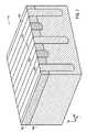
- FIGS. 13 and 14illustrate a sacrificial material 146 (which in this embodiment functions as, and may be referred to as a mold) that may be formed against the sidewalls of the fin rows 142 .
- the sacrificial material 142may be formed with a sidewall spacer process.
- Sacrificial material 142may be formed from a material that may become flowable (e.g., it may become a fluid, such as a gas or a liquid) under procession conductions subsequently described with reference to FIG. 18 .
- Examples of disposable-mold materialsinclude carbon and certain polymers, both of which may be removed from the substrate 110 as a gas by reacting them with oxygen in a furnace.
- a conformal filmmay be deposited on the substrate 110 , covering the upper doped region 112 and the lower doped region 114 , and subsequently is anisotropically etched.
- the sidewall spacer etchmay remove a portion of the lower doped region 114 to form recesses 148 .
- the recesses 148may have a width 150 generally equal to or less than 1 F, 1 ⁇ 2 F, or 1 ⁇ 4 F.
- continuing the sidewall spacer etch until it forms recesses 148is believed to reduce the likelihood of gates formed with the molds 146 shorting to one another.
- the sacrificial material 146extends above the bottom of the upper doped region 112 and has a width 152 that may be less than or generally equal to 1 F, 1 ⁇ 2 F, or 1 ⁇ 4 F.
- a dielectric region 154may be formed over the sacrificial material 146 , as illustrated by FIG. 15 .
- the dielectric region 154may be an oxide deposited with a low-temperature process, such as atomic-layer-deposition (ALD).
- ALDatomic-layer-deposition
- the illustrated dielectric 154substantially or entirely envelops the sacrificial material 146 and includes an overburden 156 .
- the overburden 156is consumed in a planarization step illustrated by FIG. 16 .
- the substrate 110may be planarized with an etch back, CMP, or other processes.
- the overburden 156may be removed until the top of the upper doped region 112 , the deep isolation trench 118 , and the shallow trenches 130 are exposed.
- the transition between the dielectric region 154 and these structures 112 , 118 , and 130may produce a phenomenon that triggers an endpoint to the process used to planarize the substrate 110 .
- this transitionmay yield a change in the optical properties of the substrate 110 (such as color), a change in the chemical properties of waste material leaving the substrate 110 (such as waste gases in an etch chamber or slurry pH), or a change in the mechanical properties of the substrate 110 (such as sliding friction).
- a change in the optical properties of the substrate 110such as color
- a change in the chemical properties of waste material leaving the substrate 110such as waste gases in an etch chamber or slurry pH
- a change in the mechanical properties of the substrate 110such as sliding friction
- this materialis a nitride, and it is removed with a dry etch that is selective against silicon and oxide to avoid losing substantial amounts of these materials. Clearing at least a portion of the shallow trenches 130 opens a passage to a sidewall 158 of the sacrificial material 146 , and this passage may facilitate removal of the sacrificial material 146 .
- the sacrificial material 146may be removed by way of the open passage through the shallow isolation trench 130 , as illustrated by FIG. 18 .
- the substrate 110may be exposed to an oxygen plasma, e.g., in a plasma etch chamber, or oxygen in a furnace.
- the plasma or other reactantsflow in through the shallow isolation trench 130 and react with the sidewall 158 of the sacrificial material 146 , e.g., by combusting the sacrificial material 146 .
- the byproducts of the reactionare gases, e.g. steam, carbon monoxide, and carbon dioxide, and the gases flow back out through the shallow isolation trench 130 .
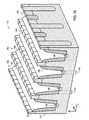
- combustioncontinues until a substantial portion or substantially the entire sacrificial material 146 is burned and cavities 160 are formed.
- the resulting cavities 160are bounded on one side by the dielectric 154 and on another side by the fin rows 142 .
- FIG. 19illustrates cavities 160 without the other parts of substrate 110 .
- Each of the cavities 160may includes two generally reflectively symmetric, generally linear, and generally parallel voids 162 and 164 and a plurality of trench segments 166 .
- the illustrated trench segments 166are disposed in a top portion of the voids 162 and 164 and join the voids 162 and 164 to one another.
- Adjacent cavities 160may be substantially or entirely separated from one another by the dielectric 154 ( FIG. 18 ).
- a gate dielectric 166may be formed within the cavities 160 , as illustrated by FIG. 20 .
- the gate dielectric 166may be either deposited, e.g., with CVD, or grown by exposing the substrate 110 to oxygen.
- the gate dielectric 166is grown by reacting silicon portions of the substrate 110 with oxygen, so the gate dielectric 166 is disposed on the exposed surfaces of the fin rows 142 , including the surface of the shallow trench 130 .
- the oxygen or other chemicals that react to form the gate dielectric 166flow into the cavities 160 through the trench segments 166 and reacts with surfaces within the linear voids 162 and 164 ( FIG. 19 ).
- the gate dielectric 166may be made from a variety of materials, including oxide, oxynitride, a hafnium-based high-k dielectric, or other appropriate materials.
- gate materialmay be deposited within the cavities 166 to form gates 168 , as illustrated by FIGS. 21 , 22 and 23 .
- the illustrated gates 168may be formed by depositing titanium nitride or other appropriate conductive materials.
- the gate materialmay be conveyed to the substrate 110 and into the cavities 166 by gas-phase reactants. The reactants may flow into the cavities 166 through the shallow trench 130 and react on the surface of the cavities 166 . In some embodiments, the gate material closes the shallow trench 130 before the cavities 166 are filled, thereby leaving voids 170 .
- An overburden of gate materialmay form on the surface of the substrate 110 , and the overburden may be removed with a wet etch, a dry etch, or a CMP process.
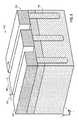
- FIG. 24is an exploded, perspective view of an example of a transistor 171 formed with the above-described process.
- the illustrated transistor 171includes a fin 172 , the gate dielectric 166 , and the gate 168 .
- the illustrated fin 172includes two legs 174 and 176 separated by a generally U-shaped slot 178 corresponding with the shallow trench 130 .
- a distal portion of the fin 172is made from the upper doped region 112
- a lower portion of the fin 172is made from the lower doped region 114 .
- Edges 180 and 182are generally defined by the deep isolation trenches 118 and may be longer than sides 184 and 185 of the fin 172 .
- the illustrated gate 166is disposed adjacent both the sides 184 and 185 and the surface of the slot 178 .
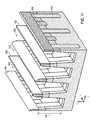
- the gate 168includes two side gates 186 and 188 and a top gate 190 .
- the two side gates 186 and 188are generally reflectively symmetric and both generally extend in the X direction with a generally uniform cross-section over a substantial distance.
- the shape of the side gates 186 and 188is generally complementary to the shape of the sacrificial material 146 with the exception of the voids 170 .
- the illustrated top gate 190has a generally uniform cross-section in the Y direction and it joins the side gates 186 and 188 to one another.
- the top gate 190may be generally solid, without a void, or in some embodiments, the top gate 190 may also include a void.
- the side gate 186is disposed at least partially adjacent the side 185 of the fin 172
- the top gate 190is disposed at least partially within the slot 178
- the side gate 188is disposed at least partially adjacent the side 184 of the fin 172 .
- the illustrated transistor 171may be characterized as a tri-gate transistor, because the gate 168 is disposed adjacent two sides and a top portion of the fin 172 .
- the two legs 174 and 176may function as a source and a drain, and the transistor 171 may selectively control the flow of current between the source and the drain according to a voltage of the gate 168 .
- the illustrated transistor 171includes three channels: a generally horizontal channel represented by arrows 192 and two generally vertical channels represented by arrows 194 .
- the generally horizontal channel 192may be established by electric fields emanating from the top gate 190
- the generally vertical channels 194may be established by electric fields emanating from the two side gates 186 and 188 .
Landscapes
- Engineering & Computer Science (AREA)
- Physics & Mathematics (AREA)
- Condensed Matter Physics & Semiconductors (AREA)
- General Physics & Mathematics (AREA)
- Manufacturing & Machinery (AREA)
- Computer Hardware Design (AREA)
- Microelectronics & Electronic Packaging (AREA)
- Power Engineering (AREA)
- Insulated Gate Type Field-Effect Transistor (AREA)
- Element Separation (AREA)
- Thin Film Transistor (AREA)
Abstract
Description
- This application is a divisional of U.S. patent application Ser. No. 12/043,813, which was filed on Mar. 6, 2008.
- 1. Field of Invention
- Embodiments of the present invention relate generally to electronic devices and, more specifically, in certain embodiments, to fin field-effect transistors.
- 2. Description of Related Art
- Fin field-effect transistors (finFETs) are often built around a fin (e.g., a tall, thin semiconductive member) rising generally perpendicularly from a substrate. Typically, a gate traverses the fin by conformally running up one side of the fin, over the top, and down the other side of the fin. In some instances, the gate is disposed against the sides of the fin and does not extend over the top. Generally, a source and a drain are located on opposite sides of the gate near the ends of the fin. In operation, a current through the fin between the source and drain is controlled by selectively energizing the gate.
- Some finFETs include gates formed with a sidewall-spacer process. In some versions of this process, the gates are formed by covering a fin with a conformal, conductive film and, then, anisotropically etching the conductive film. During the etch, the conductive material is removed faster from the horizontal surfaces than from the vertical surfaces. As a result, a portion of the conductive material remains against the vertical sidewalls of the fins, thereby forming the gate. An advantage of this process is that relatively narrow gates can be formed relative to gates patterned with photolithography, which is often subject to alignment and resolution constraints.
- Although forming gates with a sidewall-spacer process avoids some process issues, it can introduce other failure mechanisms. Often the sidewalls of the fins are angled rather than vertical because the fins were formed with an etch step that was less than perfectly anisotropic. These angled sidewalls can narrow, and in some cases close, the process window for the sidewall spacer process. The angles place the bases of adjacent fins closer to one another, and when the conformal film is deposited in this narrower gap, the portions of the film covering the adjacent sidewalls can join, creating a film with a larger vertical thickness in the gap. The film can become so thick in the gap that the sidewall-spacer etch does not remove all of the conductive film between adjacent gates. The resulting conductive residue forms stringers that short adjacent finFETs and lower yields.
FIGS. 1-24 illustrate an example of a manufacturing process in accordance with an embodiment of the present technique.- Some of the problems discussed above may be mitigated by certain embodiments of a new manufacturing process. In one embodiment described below, gates are formed in insulated caverns along the sides of fins. The caverns of this embodiment are constructed by forming a carbon mold in the shape of the gates, covering the carbon mold with an insulator, and then removing the carbon mold from under the insulator by combusting the mold. The resulting cavities are then at least partially filled with a gate insulator and a conductive gate material to form transistors. Because the cavities are insulated from one another before the gates are formed, the gates are believed to be less likely to short to other gates. This process and others are described below with reference to
FIGS. 1-24 . - As illustrated by
FIG. 1 , the manufacturing process begins with providing asubstrate 110. Thesubstrate 110 may include semiconductive materials such as single crystal or poly-crystalline silicon, gallium arsenide, indium phosphide, or other materials with semiconductor properties. Alternately, or additionally, thesubstrate 110 may include a non-semiconductor surface on which an electronic device may be constructed such as a plastic or ceramic work surface, for example. The term “substrate” encompasses bodies in a variety of stages of manufacture, including an unprocessed whole wafer, a partially-processed whole wafer, a fully-processed whole wafer, a portion of a diced wafer, or a portion of a diced wafer in a packaged electronic device. - In this embodiment, the
substrate 110 includes an upperdoped region 112 and a lowerdoped region 114. The upperdoped region 112 and the lowerdoped region 114 may be differently doped. For example, the upperdoped region 112 may include an n+material and the lowerdoped region 114 may include a p-material. The depth of the upperdoped region 112 may be generally uniform over a substantial portion of thesubstrate 110, such as throughout a substantial portion of an array area of a memory device, for example. The upper dopedregion 112 and lowerdoped region 114 may be formed by implanting or diffusing dopant materials. Alternatively, or additionally, one or both of theseregions 112 and/or114 may be doped during growth or deposition of all or part of thesubstrate 110, such as during epitaxial deposition of a semiconductive material or during growth of a semiconductive ingot from which wafers may be cut. As explained below, the upperdoped region 112 may provide material used to form a source and a drain of a transistor, and the lowerdoped region 114 may provide material used to form a channel of the transistor. - Next, a
deep trench mask 116 is formed, as illustrated byFIG. 2 , anddeep isolation trenches 118 are etched, as illustrated byFIG. 3 . Thedeep trench mask 116 may be photoresist or a hard mask, and thedeep trench mask 116 may be patterned with photolithography equipment or other types of lithographic equipment, such as a nano-imprint system or an electron beam system. Thedeep trench mask 116 includes generally linear and generally parallel exposed regions with a width120 generally equal to or less than ¼ F, ½ F or F and masked regions with a width122 generally equal to or less than ¾ F, 3/2 F, or 3 F, where F is the resolution of the system used to pattern thedeep trench mask 116. - In some embodiments, the
deep trench mask 116 is formed by double pitching a mask (not shown). In one example of such a process, thedeep trench mask 116 is formed first by masking off the areas between every other pair of exposed regions and, then, forming a poly-silicon sidewall spacer on the sides of the mask, over the areas corresponding to each of the exposed regions. Then the initial mask may be removed and a hard mask material, such as oxide, may be deposited over the remaining poly-silicon sidewall spacers, and the hard mask material may be etched back or planarized with chemical mechanical planarization (CMP) to expose the poly-silicon. Next, the poly-silicon may be selectively etched to form the exposed regions the oxide hard mask illustrated byFIG. 2 . Because the width122 of the exposed regions is generally defined by the width of a sidewall spacer, in some embodiments, the width122 may be smaller than F. - As illustrated by
FIG. 3 , the regions of thesubstrate 110 exposed by themask 116 may be etched to form thedeep isolation trenches 118. In this embodiment, the etch is a generally anisotropic dry etch. Thedeep isolation trenches 118 may generally extend laterally in the Y direction and downward in the Z direction. Thedeep isolation trenches 118 may have a generally rectangular or trapezoidal cross-section, and, in some embodiments, their cross-section may be generally uniform through some distance in the Y-direction. - Next in the present embodiment, the
deep trench mask 116 is removed, and thedeep isolation trenches 118 are filled with a dielectric, as illustrated byFIG. 4 . Thedeep trench mask 116 may be removed with a variety of techniques, such as reacting photoresist with oxygen in a furnace or in a plasma etch chamber or selectively wet etching the mask material. In some embodiments, thedeep trench mask 116 is removed after filling thedeep isolation trenches 118. In others,deep trench mask 116 may be removed prior to filing thedeep isolation trenches 118. For example, a dielectric overburden may be deposited both over thedeep trench mask 116 and in thedeep isolation trenches 118, and thedeep trench mask 116 may serve as a stop region during chemical-mechanical planarization (CMP) to remove the overburden. Thedeep isolation trenches 118 may be partially or entirely filled with various dielectric materials, such as high-density-plasma (HDP) oxide, spun-on-glass (SOG), or tetra-ethyl-ortho-silicate (TEOS), among others, to electrically isolate features. To further isolate features, in some embodiments, the bottom of thedeep isolation trenches 118 may be implanted with a dopant selected to enhance isolation prior to filling thetrenches 118. Additionally, thedeep isolation trenches 118 may include various liner materials, such as silicon nitride for example, to relieve film stresses, improve adhesion, or function as a barrier material. - After filling the
deep isolation trenches 118, ashallow trench mask 124 is formed on thesubstrate 110, as illustrated byFIG. 5 . As with thedeep trench mask 116, theshallow trench mask 124 may be photoresist or a hard mask, and it may be patterned with various lithographic systems, such as those discussed above. In some embodiments, theshallow trench mask 124 is a hard mask formed with a double-pitched-mask process similar to the process described above for theisolation trench mask 116, except that this mask is shifted in the X direction by ½ pitch. The illustratedshallow trench mask 124 includes exposed regions with aspace 126 that may have a width generally equal to or less than ¼ F, ½ F or F and covered regions with awidth 128 that may be generally equal to or less than ¾ F, 3/2 F, or 3 F. The exposed regions may be generally linear, generally parallel, and interposed generally equidistant between thedeep isolation trenches 118. - Next, the exposed regions of the
substrate 110 may be etched to formshallow trenches 130, as illustrated byFIG. 6 . Theshallow trenches 130 may be generally linear, generally parallel, generally extend generally laterally in the Y direction and generally downward in the Z direction, and thus, may be generally parallel to thedeep isolation trenches 118. In this embodiment, theshallow trenches 130 are formed with a generally anisotropic dry etch and are deeper than the upperdoped region 112, but not as deep as thedeep isolation trenches 118. Theshallow trenches 130 may have a generally rectangular or generally trapezoidal profile that is generally uniform in the Y direction over a substantial distance. - As illustrated by
FIG. 7 , theshallow trenches 130 are filled with a sacrificial material, such as nitride. In this embodiment, theshallow trenches 130 are filled with a different material from thedeep isolation trenches 118 so that theshallow trenches 130 can be selectively etched in a subsequent step without removing substantial amounts of material from thedeep isolation trenches 118. In other embodiments though, thesetrenches - Next, a
fin mask 132 is formed, as illustrated byFIG. 8 . Thefin mask 132 may be made of photoresist, or it may be a hard mask. Thefin mask 132 may be patterned with any of the lithographic systems described above or others. In this embodiment, thefin mask 132 defines a masked region with awidth 134 and exposed regions with awidth 136. Thewidth 134 may be generally equal to or less than F, and thewidth 136 may be generally equal to or less than 3/2 F. The masked regions may be generally straight, generally parallel to one another, and are generally perpendicular to both thedeep isolation trenches 118 and theshallow trenches 130, and generally extend in the X direction. - In some embodiments, the
fin mask 132 is double pitched.Sidewall spacers 138 may be formed against the sidewalls of thefin mask 132, as illustrated byFIG. 9 . The sidewall spacers138 may be formed by depositing a conformal film on thesubstrate 110 and anisotropically etching the conformal film to remove it from the horizontal surfaces. The sidewall spacers138 may be made of a different material from thefin mask 132 to facilitate selective removal of thefin mask 132 in a subsequent step. The sidewall spacers138 may have awidth 140 that is generally equal to or less than ¼ F, ½ F, or F. - Next, the
fin mask 132 is removed, as illustrated byFIG. 10 , andfin rows 142 are formed, as illustrated byFIG. 11 . Thefin mask 132 may be removed with an etch or other process that selectively removes the fin mask material at a substantially higher rate than the other materials of thesubstrate 110. Each of the exposedsidewall spacers 138 may mask an area that generally corresponds with the top of thefin rows 142. In this embodiment, thefin rows 142 are etched with a generally anisotropic etch to adepth 144 that is generally greater than the depth of theshallow trenches 130, but not as deep as thedeep isolation trenches 118. Thefin rows 142 may have a generally trapezoidal cross-section that extends generally uniformly in the X direction over a substantial distance. In other embodiments, thefin rows 142 may have other profiles, such as generally rectangular or curved profiles. - Next, the
spacers 138 may be removed, as illustrated byFIG. 12 , or in some embodiments, thespacers 138 may be left on thefin rows 142 and removed during a subsequent step. FIGS. 13 and 14 illustrate a sacrificial material146 (which in this embodiment functions as, and may be referred to as a mold) that may be formed against the sidewalls of thefin rows 142. Thesacrificial material 142 may be formed with a sidewall spacer process.Sacrificial material 142 may be formed from a material that may become flowable (e.g., it may become a fluid, such as a gas or a liquid) under procession conductions subsequently described with reference toFIG. 18 . Examples of disposable-mold materials include carbon and certain polymers, both of which may be removed from thesubstrate 110 as a gas by reacting them with oxygen in a furnace. A conformal film may be deposited on thesubstrate 110, covering the upperdoped region 112 and the lower dopedregion 114, and subsequently is anisotropically etched. The sidewall spacer etch may remove a portion of the lower dopedregion 114 to form recesses148. Therecesses 148 may have awidth 150 generally equal to or less than 1 F, ½ F, or ¼ F. As explained below, continuing the sidewall spacer etch until it forms recesses148 is believed to reduce the likelihood of gates formed with themolds 146 shorting to one another. In this embodiment, thesacrificial material 146 extends above the bottom of the upperdoped region 112 and has awidth 152 that may be less than or generally equal to 1 F, ½ F, or ¼ F.- After forming the
sacrificial material 146, adielectric region 154 may be formed over thesacrificial material 146, as illustrated byFIG. 15 . In some embodiments, thedielectric region 154 may be an oxide deposited with a low-temperature process, such as atomic-layer-deposition (ALD). The illustrated dielectric154 substantially or entirely envelops thesacrificial material 146 and includes anoverburden 156. - The
overburden 156 is consumed in a planarization step illustrated byFIG. 16 . Thesubstrate 110 may be planarized with an etch back, CMP, or other processes. In some embodiments, theoverburden 156 may be removed until the top of the upperdoped region 112, thedeep isolation trench 118, and theshallow trenches 130 are exposed. The transition between thedielectric region 154 and thesestructures substrate 110. For example, this transition may yield a change in the optical properties of the substrate110 (such as color), a change in the chemical properties of waste material leaving the substrate110 (such as waste gases in an etch chamber or slurry pH), or a change in the mechanical properties of the substrate110 (such as sliding friction). - Next, at least a portion of the material in the
shallow trenches 130 may be removed, as illustrated byFIG. 17 . In some embodiments, this material is a nitride, and it is removed with a dry etch that is selective against silicon and oxide to avoid losing substantial amounts of these materials. Clearing at least a portion of theshallow trenches 130 opens a passage to asidewall 158 of thesacrificial material 146, and this passage may facilitate removal of thesacrificial material 146. - The
sacrificial material 146 may be removed by way of the open passage through theshallow isolation trench 130, as illustrated byFIG. 18 . To remove thesacrificial material 146, thesubstrate 110 may be exposed to an oxygen plasma, e.g., in a plasma etch chamber, or oxygen in a furnace. The plasma or other reactants flow in through theshallow isolation trench 130 and react with thesidewall 158 of thesacrificial material 146, e.g., by combusting thesacrificial material 146. In some embodiments, the byproducts of the reaction are gases, e.g. steam, carbon monoxide, and carbon dioxide, and the gases flow back out through theshallow isolation trench 130. In some embodiments, combustion continues until a substantial portion or substantially the entiresacrificial material 146 is burned andcavities 160 are formed. The resultingcavities 160 are bounded on one side by the dielectric154 and on another side by thefin rows 142. - The shape of the
cavities 160 is illustrated byFIG. 19 , which illustratescavities 160 without the other parts ofsubstrate 110. Each of thecavities 160 may includes two generally reflectively symmetric, generally linear, and generallyparallel voids trench segments 166. The illustratedtrench segments 166 are disposed in a top portion of thevoids voids Adjacent cavities 160 may be substantially or entirely separated from one another by the dielectric154 (FIG. 18 ). - Next, a
gate dielectric 166 may be formed within thecavities 160, as illustrated byFIG. 20 . Thegate dielectric 166 may be either deposited, e.g., with CVD, or grown by exposing thesubstrate 110 to oxygen. In the illustrated embodiment, thegate dielectric 166 is grown by reacting silicon portions of thesubstrate 110 with oxygen, so thegate dielectric 166 is disposed on the exposed surfaces of thefin rows 142, including the surface of theshallow trench 130. The oxygen or other chemicals that react to form thegate dielectric 166 flow into thecavities 160 through thetrench segments 166 and reacts with surfaces within thelinear voids 162 and164 (FIG. 19 ). In various embodiments, thegate dielectric 166 may be made from a variety of materials, including oxide, oxynitride, a hafnium-based high-k dielectric, or other appropriate materials. - Once the
gate dielectric 166 is formed, gate material may be deposited within thecavities 166 to formgates 168, as illustrated byFIGS. 21 ,22 and23. The illustratedgates 168 may be formed by depositing titanium nitride or other appropriate conductive materials. The gate material may be conveyed to thesubstrate 110 and into thecavities 166 by gas-phase reactants. The reactants may flow into thecavities 166 through theshallow trench 130 and react on the surface of thecavities 166. In some embodiments, the gate material closes theshallow trench 130 before thecavities 166 are filled, thereby leavingvoids 170. An overburden of gate material may form on the surface of thesubstrate 110, and the overburden may be removed with a wet etch, a dry etch, or a CMP process. FIG. 24 is an exploded, perspective view of an example of a transistor171 formed with the above-described process. It should be noted, though, that the present technique is not limited to transistors and may be used to form other devices, such as capacitors or floating-gate transistors. The illustrated transistor171 includes afin 172, thegate dielectric 166, and thegate 168. The illustratedfin 172 includes twolegs U-shaped slot 178 corresponding with theshallow trench 130. A distal portion of thefin 172 is made from the upperdoped region 112, and a lower portion of thefin 172 is made from the lower dopedregion 114.Edges deep isolation trenches 118 and may be longer thansides fin 172. The illustratedgate 166 is disposed adjacent both thesides slot 178.- In the illustrated embodiment, the
gate 168 includes twoside gates top gate 190. The twoside gates side gates sacrificial material 146 with the exception of thevoids 170. The illustratedtop gate 190 has a generally uniform cross-section in the Y direction and it joins theside gates top gate 190 may be generally solid, without a void, or in some embodiments, thetop gate 190 may also include a void. Theside gate 186 is disposed at least partially adjacent theside 185 of thefin 172, thetop gate 190 is disposed at least partially within theslot 178, and theside gate 188 is disposed at least partially adjacent theside 184 of thefin 172. The illustrated transistor171 may be characterized as a tri-gate transistor, because thegate 168 is disposed adjacent two sides and a top portion of thefin 172. - In operation, the two
legs gate 168. The illustrated transistor171 includes three channels: a generally horizontal channel represented byarrows 192 and two generally vertical channels represented byarrows 194. The generallyhorizontal channel 192 may be established by electric fields emanating from thetop gate 190, and the generallyvertical channels 194 may be established by electric fields emanating from the twoside gates - While the invention may be susceptible to various modifications and alternative forms, specific embodiments have been shown by way of example in the drawings and have been described in detail herein. However, it should be understood that the invention is not intended to be limited to the particular forms disclosed. Rather, the invention is to cover all modifications, equivalents, and alternatives falling within the spirit and scope of the invention as defined by the following appended claims.
Claims (22)
Priority Applications (2)
| Application Number | Priority Date | Filing Date | Title |
|---|---|---|---|
| US13/028,064US8669159B2 (en) | 2008-03-06 | 2011-02-15 | Devices with cavity-defined gates and methods of making the same |
| US14/198,937US9331203B2 (en) | 2008-03-06 | 2014-03-06 | Devices with cavity-defined gates and methods of making the same |
Applications Claiming Priority (2)
| Application Number | Priority Date | Filing Date | Title |
|---|---|---|---|
| US12/043,813US7915659B2 (en) | 2008-03-06 | 2008-03-06 | Devices with cavity-defined gates and methods of making the same |
| US13/028,064US8669159B2 (en) | 2008-03-06 | 2011-02-15 | Devices with cavity-defined gates and methods of making the same |
Related Parent Applications (1)
| Application Number | Title | Priority Date | Filing Date |
|---|---|---|---|
| US12/043,813DivisionUS7915659B2 (en) | 2008-03-06 | 2008-03-06 | Devices with cavity-defined gates and methods of making the same |
Related Child Applications (1)
| Application Number | Title | Priority Date | Filing Date |
|---|---|---|---|
| US14/198,937ContinuationUS9331203B2 (en) | 2008-03-06 | 2014-03-06 | Devices with cavity-defined gates and methods of making the same |
Publications (2)
| Publication Number | Publication Date |
|---|---|
| US20110143528A1true US20110143528A1 (en) | 2011-06-16 |
| US8669159B2 US8669159B2 (en) | 2014-03-11 |
Family
ID=40551557
Family Applications (3)
| Application Number | Title | Priority Date | Filing Date |
|---|---|---|---|
| US12/043,813Active2028-07-05US7915659B2 (en) | 2008-03-06 | 2008-03-06 | Devices with cavity-defined gates and methods of making the same |
| US13/028,064Active2028-12-26US8669159B2 (en) | 2008-03-06 | 2011-02-15 | Devices with cavity-defined gates and methods of making the same |
| US14/198,937Active2028-08-10US9331203B2 (en) | 2008-03-06 | 2014-03-06 | Devices with cavity-defined gates and methods of making the same |
Family Applications Before (1)
| Application Number | Title | Priority Date | Filing Date |
|---|---|---|---|
| US12/043,813Active2028-07-05US7915659B2 (en) | 2008-03-06 | 2008-03-06 | Devices with cavity-defined gates and methods of making the same |
Family Applications After (1)
| Application Number | Title | Priority Date | Filing Date |
|---|---|---|---|
| US14/198,937Active2028-08-10US9331203B2 (en) | 2008-03-06 | 2014-03-06 | Devices with cavity-defined gates and methods of making the same |
Country Status (6)
| Country | Link |
|---|---|
| US (3) | US7915659B2 (en) |
| JP (1) | JP5360507B2 (en) |
| KR (1) | KR101547375B1 (en) |
| CN (1) | CN101960572B (en) |
| TW (1) | TWI430371B (en) |
| WO (1) | WO2009111225A1 (en) |
Cited By (3)
| Publication number | Priority date | Publication date | Assignee | Title |
|---|---|---|---|---|
| US20130059401A1 (en)* | 2011-09-01 | 2013-03-07 | Gaku Sudo | Method for manufacturing semiconductor device |
| US20130244392A1 (en)* | 2012-03-19 | 2013-09-19 | Samsung Electronics Co., Ltd. | Method of fabricating fin-field effect transistors (finfets) having different fin widths |
| CN103531467A (en)* | 2012-07-02 | 2014-01-22 | 中芯国际集成电路制造(上海)有限公司 | Semiconductor device and forming method thereof |
Families Citing this family (33)
| Publication number | Priority date | Publication date | Assignee | Title |
|---|---|---|---|---|
| US7898857B2 (en) | 2008-03-20 | 2011-03-01 | Micron Technology, Inc. | Memory structure having volatile and non-volatile memory portions |
| US8546876B2 (en) | 2008-03-20 | 2013-10-01 | Micron Technology, Inc. | Systems and devices including multi-transistor cells and methods of using, making, and operating the same |
| US7969776B2 (en) | 2008-04-03 | 2011-06-28 | Micron Technology, Inc. | Data cells with drivers and methods of making and operating the same |
| KR20090105700A (en)* | 2008-04-03 | 2009-10-07 | 주식회사 하이닉스반도체 | Manufacturing method of semiconductor device |
| US8704375B2 (en)* | 2009-02-04 | 2014-04-22 | Taiwan Semiconductor Manufacturing Company, Ltd. | Barrier structures and methods for through substrate vias |
| JP5718585B2 (en)* | 2010-05-19 | 2015-05-13 | ピーエスフォー ルクスコ エスエイアールエルPS4 Luxco S.a.r.l. | Semiconductor device, manufacturing method thereof, and data processing system |
| DE102010030760B4 (en)* | 2010-06-30 | 2014-07-24 | Globalfoundries Dresden Module One Limited Liability Company & Co. Kg | Semiconductor device with via contacts with a stress relaxation mechanism and method of making the same |
| US8334196B2 (en) | 2010-11-01 | 2012-12-18 | Micron Technology, Inc. | Methods of forming conductive contacts in the fabrication of integrated circuitry |
| US9553193B2 (en) | 2010-11-19 | 2017-01-24 | Micron Technology, Inc. | Double gated fin transistors and methods of fabricating and operating the same |
| US8294511B2 (en) | 2010-11-19 | 2012-10-23 | Micron Technology, Inc. | Vertically stacked fin transistors and methods of fabricating and operating the same |
| US8293602B2 (en) | 2010-11-19 | 2012-10-23 | Micron Technology, Inc. | Method of fabricating a finFET having cross-hair cells |
| US8921899B2 (en) | 2010-11-19 | 2014-12-30 | Micron Technology, Inc. | Double gated 4F2 dram CHC cell and methods of fabricating the same |
| US8969154B2 (en)* | 2011-08-23 | 2015-03-03 | Micron Technology, Inc. | Methods for fabricating semiconductor device structures and arrays of vertical transistor devices |
| US9461143B2 (en) | 2012-09-19 | 2016-10-04 | Intel Corporation | Gate contact structure over active gate and method to fabricate same |
| US20140103452A1 (en)* | 2012-10-15 | 2014-04-17 | Marvell World Trade Ltd. | Isolation components for transistors formed on fin features of semiconductor substrates |
| US9263585B2 (en)* | 2012-10-30 | 2016-02-16 | Globalfoundries Inc. | Methods of forming enhanced mobility channel regions on 3D semiconductor devices, and devices comprising same |
| US8946050B2 (en)* | 2012-10-30 | 2015-02-03 | Globalfoundries Inc. | Double trench well formation in SRAM cells |
| CN103855026B (en)* | 2012-12-06 | 2017-04-19 | 中国科学院微电子研究所 | Finfet and manufacturing method thereof |
| CN103928334B (en)* | 2013-01-15 | 2017-06-16 | 中国科学院微电子研究所 | Semiconductor device and method for manufacturing the same |
| JP2014222682A (en)* | 2013-05-13 | 2014-11-27 | ピーエスフォー ルクスコ エスエイアールエルPS4 Luxco S.a.r.l. | Semiconductor device and method of manufacturing the same |
| US9343320B2 (en) | 2013-12-06 | 2016-05-17 | Globalfoundries Inc. | Pattern factor dependency alleviation for eDRAM and logic devices with disposable fill to ease deep trench integration with fins |
| US9871121B2 (en) | 2014-03-10 | 2018-01-16 | Qualcomm Incorporated | Semiconductor device having a gap defined therein |
| TWI642110B (en)* | 2014-12-03 | 2018-11-21 | 聯華電子股份有限公司 | Semiconductor component and manufacturing method thereof |
| US9466602B1 (en) | 2015-06-15 | 2016-10-11 | International Business Machines Corporation | Embedded dynamic random access memory field effect transistor device |
| US9553194B1 (en)* | 2015-07-29 | 2017-01-24 | Globalfoundries Inc. | Method for improved fin profile |
| CN106611787A (en)* | 2015-10-26 | 2017-05-03 | 联华电子股份有限公司 | Semiconductor structure and manufacturing method thereof |
| US10504821B2 (en)* | 2016-01-29 | 2019-12-10 | United Microelectronics Corp. | Through-silicon via structure |
| US9691864B1 (en)* | 2016-05-13 | 2017-06-27 | Infineon Technologies Americas Corp. | Semiconductor device having a cavity and method for manufacturing thereof |
| US10157745B2 (en)* | 2016-06-29 | 2018-12-18 | International Business Machines Corporation | High aspect ratio gates |
| US9934970B1 (en)* | 2017-01-11 | 2018-04-03 | International Business Machines Corporation | Self aligned pattern formation post spacer etchback in tight pitch configurations |
| US10770571B2 (en)* | 2018-09-19 | 2020-09-08 | Taiwan Semiconductor Manufacturing Co., Ltd. | FinFET with dummy fins and methods of making the same |
| US20220231023A1 (en)* | 2021-01-15 | 2022-07-21 | Taiwan Semiconductor Manufacturing Co., Ltd. | Finfet device and method |
| CN118738121A (en)* | 2024-04-15 | 2024-10-01 | 华南师范大学 | Based on multi-region gate single-channel microcavity transistor, optoelectronic full logic gate device, control method and circuit |
Citations (39)
| Publication number | Priority date | Publication date | Assignee | Title |
|---|---|---|---|---|
| US5160987A (en)* | 1989-10-26 | 1992-11-03 | International Business Machines Corporation | Three-dimensional semiconductor structures formed from planar layers |
| US5661061A (en)* | 1994-03-25 | 1997-08-26 | Hitachi, Ltd. | Process for fabricating a semiconductor integrated circuit device having the multi-layered fin structure |
| US5858829A (en)* | 1998-06-29 | 1999-01-12 | Vanguard International Semiconductor Corporation | Method for fabricating dynamic random access memory (DRAM) cells with minimum active cell areas using sidewall-spacer bit lines |
| US6081008A (en)* | 1996-02-14 | 2000-06-27 | Lsi Logic Corporation | Composite trench-fin capacitors for DRAM |
| US6100129A (en)* | 1998-11-09 | 2000-08-08 | Worldwide Semiconductor Manufacturing Corporation | Method for making fin-trench structured DRAM capacitor |
| US6258656B1 (en)* | 1998-09-17 | 2001-07-10 | Siemens Aktiengesellschaft | Capacitor with high-ε dielectric or ferroelectric material based on the fin stack principle and production process using a negative mold |
| US6258559B1 (en)* | 1999-03-22 | 2001-07-10 | Zymogenetics, Inc. | Method for producing proteins in transformed Pichia |
| US6268243B1 (en)* | 1999-04-15 | 2001-07-31 | Hyundai Electronics Industries Co., Ltd. | Method for fabricating dynamic random access memory cells |
| US6440792B1 (en)* | 1999-11-05 | 2002-08-27 | Promos Technology, Inc. | DRAM technology of storage node formation and no conduction/isolation process of bottle-shaped deep trench |
| US20020155656A1 (en)* | 2000-07-14 | 2002-10-24 | Katsuya Hayano | Manufacturing method of semiconductor integrated circuit device, and semiconductor integrated circuit device |
| US6605514B1 (en)* | 2002-07-31 | 2003-08-12 | Advanced Micro Devices, Inc. | Planar finFET patterning using amorphous carbon |
| US20030168676A1 (en)* | 1996-07-10 | 2003-09-11 | Fujitsu Limited | Semiconductor device with self-aligned contact and its manufacture |
| US6897107B2 (en)* | 2001-04-11 | 2005-05-24 | International Business Machines Corporation | Method for forming TTO nitride liner for improved collar protection and TTO reliability |
| US20050151206A1 (en)* | 2003-12-30 | 2005-07-14 | Schwerin Ulrike G. | Transistor structure with a curved channel, memory cell and memory cell array for DRAMs, and methods for fabricating a DRAM |
| US20050196918A1 (en)* | 2004-02-10 | 2005-09-08 | Schwerin Ulrike G. | DRAM memory and method for fabricating a DRAM memory cell |
| US20050245024A1 (en)* | 2004-04-29 | 2005-11-03 | Von Schwerin Ulrike G | Method for production of trench DRAM cells and a trench DRAM cell array with fin field-effect transistors with a curved channel (CFET - curved fets) |
| US20050250285A1 (en)* | 2004-05-04 | 2005-11-10 | Jae-Man Yoon | Fin field effect transistor device and method of fabricating the same |
| US6967147B1 (en)* | 2000-11-16 | 2005-11-22 | Infineon Technologies Ag | Nitrogen implantation using a shadow effect to control gate oxide thickness in DRAM semiconductor |
| US20060006446A1 (en)* | 2004-06-29 | 2006-01-12 | Schwerin Ulrike G | Method for fabricating a DRAM memory cell arrangement having fin field effect transistors and DRAM memory cell |
| US6998666B2 (en)* | 2004-01-09 | 2006-02-14 | International Business Machines Corporation | Nitrided STI liner oxide for reduced corner device impact on vertical device performance |
| US20060057814A1 (en)* | 2004-09-10 | 2006-03-16 | Rolf Weis | Fabricating a memory cell arrangement |
| US20060073662A1 (en)* | 2004-10-02 | 2006-04-06 | Se-Myeong Jang | Method of manufacturing multi-channel transistor device and multi-channel transistor device manufactured using the method |
| US20060076602A1 (en)* | 2004-09-10 | 2006-04-13 | Johann Harter | Dram cell pair and dram memory cell array |
| US20060131651A1 (en)* | 1999-08-31 | 2006-06-22 | Kabushiki Kaisha Toshiba | Semiconductor substrate and its fabrication method |
| US20060246607A1 (en)* | 1993-04-02 | 2006-11-02 | Micron Technology, Inc. | Method for forming a storage cell capacitor compatible with high dielectric constant materials |
| US20060244106A1 (en)* | 2003-03-17 | 2006-11-02 | Kabushiki Kaisha Toshiba | Fin semiconductor device and method for fabricating the same |
| US7132333B2 (en)* | 2004-09-10 | 2006-11-07 | Infineon Technologies Ag | Transistor, memory cell array and method of manufacturing a transistor |
| US20060273415A1 (en)* | 2005-06-01 | 2006-12-07 | Hyun Jung Kim | Transistor for memory device and method for manufacturing the same |
| US20060281250A1 (en)* | 2004-12-15 | 2006-12-14 | Till Schloesser | 6F2 access transistor arrangement and semiconductor memory device |
| US20070023805A1 (en)* | 2005-07-26 | 2007-02-01 | Wells David H | Reverse construction memory cell |
| US20070111455A1 (en)* | 2005-11-14 | 2007-05-17 | Samsung Electronics Co., Ltd. | Fabrication of local damascene finFETs using contact type nitride damascene mask |
| US20070134878A1 (en)* | 2005-12-09 | 2007-06-14 | Intel Corporation | Non-planar microelectronic device having isolation element to mitigate fringe effects and method to fabricate same |
| US20070166933A1 (en)* | 2006-01-16 | 2007-07-19 | Samsung Electronics Co., Ltd. | Methods of Forming Field Effect Transistors and Capacitor-Free Dynamic Random Access Memory Cells |
| US20070170522A1 (en)* | 2006-01-23 | 2007-07-26 | Hynix Semiconductor Inc. | Semiconductor device and method for fabricating the same |
| US20070176221A1 (en)* | 1995-06-05 | 2007-08-02 | Fujitsu Limited | Semiconductor memory device and method for fabricating the same |
| US20070176253A1 (en)* | 2006-01-31 | 2007-08-02 | Peng-Fei Wang | Transistor, memory cell and method of manufacturing a transistor |
| US20070176222A1 (en)* | 1996-07-18 | 2007-08-02 | Fujitsu Limited | Highly integrated and reliable DRAM and its manufacture |
| US20070190736A1 (en)* | 2006-02-16 | 2007-08-16 | An-Hsiung Liu | Overlay alignment mark and alignment method for the fabrication of trench-capacitor dram devices |
| US20080237796A1 (en)* | 2007-03-30 | 2008-10-02 | Doyle Brian S | Increasing the surface area of a memory cell capacitor |
Family Cites Families (69)
| Publication number | Priority date | Publication date | Assignee | Title |
|---|---|---|---|---|
| US3885861A (en) | 1972-10-02 | 1975-05-27 | Hughes Aircraft Co | Liquid crystal digital reticle |
| US5196910A (en) | 1987-04-24 | 1993-03-23 | Hitachi, Ltd. | Semiconductor memory device with recessed array region |
| US5109256A (en) | 1990-08-17 | 1992-04-28 | National Semiconductor Corporation | Schottky barrier diodes and Schottky barrier diode-clamped transistors and method of fabrication |
| KR930005234B1 (en) | 1990-09-13 | 1993-06-16 | 금성일렉트론주식회사 | Cell manufacture method of fin-stack cell |
| US5864181A (en) | 1993-09-15 | 1999-01-26 | Micron Technology, Inc. | Bi-level digit line architecture for high density DRAMs |
| JP3853406B2 (en) | 1995-10-27 | 2006-12-06 | エルピーダメモリ株式会社 | Semiconductor integrated circuit device and method for manufacturing the same |
| US6043562A (en) | 1996-01-26 | 2000-03-28 | Micron Technology, Inc. | Digit line architecture for dynamic memory |
| WO1997028532A1 (en) | 1996-02-01 | 1997-08-07 | Micron Technology, Inc. | Digit line architecture for dynamic memory |
| US5793033A (en) | 1996-03-29 | 1998-08-11 | Metanetics Corporation | Portable data collection device with viewing assembly |
| US7064376B2 (en) | 1996-05-24 | 2006-06-20 | Jeng-Jye Shau | High performance embedded semiconductor memory devices with multiple dimension first-level bit-lines |
| US5821513A (en) | 1996-06-26 | 1998-10-13 | Telxon Corporation | Shopping cart mounted portable data collection device with tethered dataform reader |
| US6072209A (en) | 1997-07-08 | 2000-06-06 | Micro Technology, Inc. | Four F2 folded bit line DRAM cell structure having buried bit and word lines |
| US5925918A (en) | 1997-07-30 | 1999-07-20 | Micron, Technology, Inc. | Gate stack with improved sidewall integrity |
| US6097212A (en) | 1997-10-09 | 2000-08-01 | Lattice Semiconductor Corporation | Variable grain architecture for FPGA integrated circuits |
| US6130551A (en) | 1998-01-19 | 2000-10-10 | Vantis Corporation | Synthesis-friendly FPGA architecture with variable length and variable timing interconnect |
| US6137128A (en) | 1998-06-09 | 2000-10-24 | International Business Machines Corporation | Self-isolated and self-aligned 4F-square vertical fet-trench dram cells |
| TW388125B (en) | 1998-08-19 | 2000-04-21 | Vanguard Int Semiconduct Corp | Method for fabricating dynamic random access memory (DRAM) cells with minimum active cell areas |
| TW380316B (en) | 1998-10-15 | 2000-01-21 | Worldwide Semiconductor Mfg | Manufacturing method for fin-trench-structure capacitor of DRAM |
| US6426175B2 (en) | 1999-02-22 | 2002-07-30 | International Business Machines Corporation | Fabrication of a high density long channel DRAM gate with or without a grooved gate |
| US6282113B1 (en) | 1999-09-29 | 2001-08-28 | International Business Machines Corporation | Four F-squared gapless dual layer bitline DRAM array architecture |
| DE19946719A1 (en) | 1999-09-29 | 2001-04-19 | Infineon Technologies Ag | Trench capacitor used in the production of DRAM storage cells has a conducting contact layer between the substrate and the conducting trench filling in the trench above the insulating collar |
| WO2001061738A1 (en) | 2000-02-15 | 2001-08-23 | Steag Cvd Systems Ltd. | Dram capacitor with ultra-thin nitride layer |
| US6391753B1 (en)* | 2000-06-20 | 2002-05-21 | Advanced Micro Devices, Inc. | Process for forming gate conductors |
| KR100466689B1 (en) | 2000-08-28 | 2005-01-24 | 인터내셔널 비지네스 머신즈 코포레이션 | Compact dual-port dram architecture system and method for making same |
| US6509226B1 (en) | 2000-09-27 | 2003-01-21 | International Business Machines Corporation | Process for protecting array top oxide |
| US6258659B1 (en) | 2000-11-29 | 2001-07-10 | International Business Machines Corporation | Embedded vertical DRAM cells and dual workfunction logic gates |
| US6576944B2 (en) | 2000-12-14 | 2003-06-10 | Infineon Technologies Ag | Self-aligned nitride pattern for improved process window |
| CA2340985A1 (en) | 2001-03-14 | 2002-09-14 | Atmos Corporation | Interleaved wordline architecture |
| TW502453B (en)* | 2001-09-06 | 2002-09-11 | Winbond Electronics Corp | MOSFET and the manufacturing method thereof |
| US7190060B1 (en) | 2002-01-09 | 2007-03-13 | Bridge Semiconductor Corporation | Three-dimensional stacked semiconductor package device with bent and flat leads and method of making same |
| US7019353B2 (en) | 2002-07-26 | 2006-03-28 | Micron Technology, Inc. | Three dimensional flash cell |
| US6865100B2 (en) | 2002-08-12 | 2005-03-08 | Micron Technology, Inc. | 6F2 architecture ROM embedded DRAM |
| US7358121B2 (en)* | 2002-08-23 | 2008-04-15 | Intel Corporation | Tri-gate devices and methods of fabrication |
| US6927462B2 (en) | 2002-08-28 | 2005-08-09 | Infineon Technologes Richmond, Lp | Method of forming a gate contact in a semiconductor device |
| US6670682B1 (en) | 2002-08-29 | 2003-12-30 | Micron Technology, Inc. | Multilayered doped conductor |
| KR100481209B1 (en)* | 2002-10-01 | 2005-04-08 | 삼성전자주식회사 | MOS Transistor having multiple channels and method of manufacturing the same |
| DE10248722A1 (en) | 2002-10-18 | 2004-05-06 | Infineon Technologies Ag | Integrated circuit arrangement with capacitor and manufacturing process |
| JP3983167B2 (en)* | 2002-12-26 | 2007-09-26 | 華邦電子股▲ふん▼有限公司 | Method for manufacturing metal oxide semiconductor field effect transistor |
| DE10302128B3 (en) | 2003-01-21 | 2004-09-09 | Infineon Technologies Ag | Buffer amplifier system for buffer storage of signals runs several DRAM chips in parallel and has two output buffer amplifiers in parallel feeding reference and signal networks with capacitors and DRAMs |
| US6845033B2 (en) | 2003-03-05 | 2005-01-18 | International Business Machines Corporation | Structure and system-on-chip integration of a two-transistor and two-capacitor memory cell for trench technology |
| US6794254B1 (en) | 2003-05-15 | 2004-09-21 | Taiwan Semiconductor Manufacturing Company | Embedded dual-port DRAM process |
| US7099216B2 (en) | 2003-09-05 | 2006-08-29 | International Business Machines Corporation | Single cycle read/write/writeback pipeline, full-wordline I/O DRAM architecture with enhanced write and single ended sensing |
| US6844591B1 (en) | 2003-09-17 | 2005-01-18 | Micron Technology, Inc. | Method of forming DRAM access transistors |
| US7098105B2 (en) | 2004-05-26 | 2006-08-29 | Micron Technology, Inc. | Methods for forming semiconductor structures |
| JP4675585B2 (en)* | 2004-06-22 | 2011-04-27 | シャープ株式会社 | Field effect transistor |
| JP2006054431A (en) | 2004-06-29 | 2006-02-23 | Infineon Technologies Ag | Transistor, memory cell array, and transistor manufacturing method |
| US7442976B2 (en)* | 2004-09-01 | 2008-10-28 | Micron Technology, Inc. | DRAM cells with vertical transistors |
| US7254074B2 (en) | 2005-03-07 | 2007-08-07 | Micron Technology, Inc. | Open digit line array architecture for a memory array |
| KR100691006B1 (en)* | 2005-04-29 | 2007-03-09 | 주식회사 하이닉스반도체 | Structure of Cell Transistor of Memory Device and Manufacturing Method Thereof |
| KR100608377B1 (en)* | 2005-05-02 | 2006-08-08 | 주식회사 하이닉스반도체 | Cell transistor manufacturing method of memory device |
| US7316953B2 (en) | 2005-05-31 | 2008-01-08 | Nanya Technology Corporation | Method for forming a recessed gate with word lines |
| US7282401B2 (en) | 2005-07-08 | 2007-10-16 | Micron Technology, Inc. | Method and apparatus for a self-aligned recessed access device (RAD) transistor gate |
| US7151023B1 (en) | 2005-08-01 | 2006-12-19 | International Business Machines Corporation | Metal gate MOSFET by full semiconductor metal alloy conversion |
| US20070058468A1 (en) | 2005-09-12 | 2007-03-15 | Promos Technologies Pte.Ltd. Singapore | Shielded bitline architecture for dynamic random access memory (DRAM) arrays |
| KR100663366B1 (en) | 2005-10-26 | 2007-01-02 | 삼성전자주식회사 | Flash memory device manufacturing method having self-aligned floating gate and related devices |
| US8716772B2 (en) | 2005-12-28 | 2014-05-06 | Micron Technology, Inc. | DRAM cell design with folded digitline sense amplifier |
| JP2007294680A (en)* | 2006-04-25 | 2007-11-08 | Toshiba Corp | Semiconductor element, semiconductor device and manufacturing method thereof |
| US7573108B2 (en) | 2006-05-12 | 2009-08-11 | Micron Technology, Inc | Non-planar transistor and techniques for fabricating the same |
| KR100751803B1 (en)* | 2006-08-22 | 2007-08-23 | 삼성전자주식회사 | Manufacturing Method of Semiconductor Device |
| US7452766B2 (en)* | 2006-08-31 | 2008-11-18 | Micron Technology, Inc. | Finned memory cells and the fabrication thereof |
| KR100942961B1 (en)* | 2007-10-24 | 2010-02-17 | 주식회사 하이닉스반도체 | Manufacturing method of semiconductor device having polysilicon gate electrode of columnar structure |
| US8866254B2 (en) | 2008-02-19 | 2014-10-21 | Micron Technology, Inc. | Devices including fin transistors robust to gate shorts and methods of making the same |
| US7742324B2 (en) | 2008-02-19 | 2010-06-22 | Micron Technology, Inc. | Systems and devices including local data lines and methods of using, making, and operating the same |
| US9190494B2 (en) | 2008-02-19 | 2015-11-17 | Micron Technology, Inc. | Systems and devices including fin field-effect transistors each having U-shaped semiconductor fin |
| US8546876B2 (en) | 2008-03-20 | 2013-10-01 | Micron Technology, Inc. | Systems and devices including multi-transistor cells and methods of using, making, and operating the same |
| US7808042B2 (en) | 2008-03-20 | 2010-10-05 | Micron Technology, Inc. | Systems and devices including multi-gate transistors and methods of using, making, and operating the same |
| US7898857B2 (en) | 2008-03-20 | 2011-03-01 | Micron Technology, Inc. | Memory structure having volatile and non-volatile memory portions |
| US7969776B2 (en) | 2008-04-03 | 2011-06-28 | Micron Technology, Inc. | Data cells with drivers and methods of making and operating the same |
| US8076229B2 (en) | 2008-05-30 | 2011-12-13 | Micron Technology, Inc. | Methods of forming data cells and connections to data cells |
- 2008
- 2008-03-06USUS12/043,813patent/US7915659B2/enactiveActive
- 2009
- 2009-02-24JPJP2010549726Apatent/JP5360507B2/enactiveActive
- 2009-02-24CNCN200980107635.9Apatent/CN101960572B/enactiveActive
- 2009-02-24KRKR1020107022401Apatent/KR101547375B1/enactiveActive
- 2009-02-24WOPCT/US2009/035018patent/WO2009111225A1/enactiveApplication Filing
- 2009-03-06TWTW098107482Apatent/TWI430371B/enactive
- 2011
- 2011-02-15USUS13/028,064patent/US8669159B2/enactiveActive
- 2014
- 2014-03-06USUS14/198,937patent/US9331203B2/enactiveActive
Patent Citations (41)
| Publication number | Priority date | Publication date | Assignee | Title |
|---|---|---|---|---|
| US5160987A (en)* | 1989-10-26 | 1992-11-03 | International Business Machines Corporation | Three-dimensional semiconductor structures formed from planar layers |
| US20060246607A1 (en)* | 1993-04-02 | 2006-11-02 | Micron Technology, Inc. | Method for forming a storage cell capacitor compatible with high dielectric constant materials |
| US5661061A (en)* | 1994-03-25 | 1997-08-26 | Hitachi, Ltd. | Process for fabricating a semiconductor integrated circuit device having the multi-layered fin structure |
| US20070176221A1 (en)* | 1995-06-05 | 2007-08-02 | Fujitsu Limited | Semiconductor memory device and method for fabricating the same |
| US6081008A (en)* | 1996-02-14 | 2000-06-27 | Lsi Logic Corporation | Composite trench-fin capacitors for DRAM |
| US20030168676A1 (en)* | 1996-07-10 | 2003-09-11 | Fujitsu Limited | Semiconductor device with self-aligned contact and its manufacture |
| US20070176222A1 (en)* | 1996-07-18 | 2007-08-02 | Fujitsu Limited | Highly integrated and reliable DRAM and its manufacture |
| US5858829A (en)* | 1998-06-29 | 1999-01-12 | Vanguard International Semiconductor Corporation | Method for fabricating dynamic random access memory (DRAM) cells with minimum active cell areas using sidewall-spacer bit lines |
| US6008513A (en)* | 1998-06-29 | 1999-12-28 | Vanguard International Semiconductor Corporation | Dynamic random access memory (DRAM) cells with minimum active cell areas using sidewall-space bit lines |
| US6258656B1 (en)* | 1998-09-17 | 2001-07-10 | Siemens Aktiengesellschaft | Capacitor with high-ε dielectric or ferroelectric material based on the fin stack principle and production process using a negative mold |
| US6100129A (en)* | 1998-11-09 | 2000-08-08 | Worldwide Semiconductor Manufacturing Corporation | Method for making fin-trench structured DRAM capacitor |
| US6258559B1 (en)* | 1999-03-22 | 2001-07-10 | Zymogenetics, Inc. | Method for producing proteins in transformed Pichia |
| US6268243B1 (en)* | 1999-04-15 | 2001-07-31 | Hyundai Electronics Industries Co., Ltd. | Method for fabricating dynamic random access memory cells |
| US20060131651A1 (en)* | 1999-08-31 | 2006-06-22 | Kabushiki Kaisha Toshiba | Semiconductor substrate and its fabrication method |
| US6440792B1 (en)* | 1999-11-05 | 2002-08-27 | Promos Technology, Inc. | DRAM technology of storage node formation and no conduction/isolation process of bottle-shaped deep trench |
| US20020155656A1 (en)* | 2000-07-14 | 2002-10-24 | Katsuya Hayano | Manufacturing method of semiconductor integrated circuit device, and semiconductor integrated circuit device |
| US6967147B1 (en)* | 2000-11-16 | 2005-11-22 | Infineon Technologies Ag | Nitrogen implantation using a shadow effect to control gate oxide thickness in DRAM semiconductor |
| US6897107B2 (en)* | 2001-04-11 | 2005-05-24 | International Business Machines Corporation | Method for forming TTO nitride liner for improved collar protection and TTO reliability |
| US6605514B1 (en)* | 2002-07-31 | 2003-08-12 | Advanced Micro Devices, Inc. | Planar finFET patterning using amorphous carbon |
| US20060244106A1 (en)* | 2003-03-17 | 2006-11-02 | Kabushiki Kaisha Toshiba | Fin semiconductor device and method for fabricating the same |
| US20050151206A1 (en)* | 2003-12-30 | 2005-07-14 | Schwerin Ulrike G. | Transistor structure with a curved channel, memory cell and memory cell array for DRAMs, and methods for fabricating a DRAM |
| US20070052040A1 (en)* | 2003-12-30 | 2007-03-08 | Schwerin Ulrike G | Transistor with contoured channel and method for making the same |
| US6998666B2 (en)* | 2004-01-09 | 2006-02-14 | International Business Machines Corporation | Nitrided STI liner oxide for reduced corner device impact on vertical device performance |
| US20050196918A1 (en)* | 2004-02-10 | 2005-09-08 | Schwerin Ulrike G. | DRAM memory and method for fabricating a DRAM memory cell |
| US20050245024A1 (en)* | 2004-04-29 | 2005-11-03 | Von Schwerin Ulrike G | Method for production of trench DRAM cells and a trench DRAM cell array with fin field-effect transistors with a curved channel (CFET - curved fets) |
| US20050250285A1 (en)* | 2004-05-04 | 2005-11-10 | Jae-Man Yoon | Fin field effect transistor device and method of fabricating the same |
| US20060006446A1 (en)* | 2004-06-29 | 2006-01-12 | Schwerin Ulrike G | Method for fabricating a DRAM memory cell arrangement having fin field effect transistors and DRAM memory cell |
| US7132333B2 (en)* | 2004-09-10 | 2006-11-07 | Infineon Technologies Ag | Transistor, memory cell array and method of manufacturing a transistor |
| US20060057814A1 (en)* | 2004-09-10 | 2006-03-16 | Rolf Weis | Fabricating a memory cell arrangement |
| US20060076602A1 (en)* | 2004-09-10 | 2006-04-13 | Johann Harter | Dram cell pair and dram memory cell array |
| US20060073662A1 (en)* | 2004-10-02 | 2006-04-06 | Se-Myeong Jang | Method of manufacturing multi-channel transistor device and multi-channel transistor device manufactured using the method |
| US20060281250A1 (en)* | 2004-12-15 | 2006-12-14 | Till Schloesser | 6F2 access transistor arrangement and semiconductor memory device |
| US20060273415A1 (en)* | 2005-06-01 | 2006-12-07 | Hyun Jung Kim | Transistor for memory device and method for manufacturing the same |
| US20070023805A1 (en)* | 2005-07-26 | 2007-02-01 | Wells David H | Reverse construction memory cell |
| US20070111455A1 (en)* | 2005-11-14 | 2007-05-17 | Samsung Electronics Co., Ltd. | Fabrication of local damascene finFETs using contact type nitride damascene mask |
| US20070134878A1 (en)* | 2005-12-09 | 2007-06-14 | Intel Corporation | Non-planar microelectronic device having isolation element to mitigate fringe effects and method to fabricate same |
| US20070166933A1 (en)* | 2006-01-16 | 2007-07-19 | Samsung Electronics Co., Ltd. | Methods of Forming Field Effect Transistors and Capacitor-Free Dynamic Random Access Memory Cells |
| US20070170522A1 (en)* | 2006-01-23 | 2007-07-26 | Hynix Semiconductor Inc. | Semiconductor device and method for fabricating the same |
| US20070176253A1 (en)* | 2006-01-31 | 2007-08-02 | Peng-Fei Wang | Transistor, memory cell and method of manufacturing a transistor |
| US20070190736A1 (en)* | 2006-02-16 | 2007-08-16 | An-Hsiung Liu | Overlay alignment mark and alignment method for the fabrication of trench-capacitor dram devices |
| US20080237796A1 (en)* | 2007-03-30 | 2008-10-02 | Doyle Brian S | Increasing the surface area of a memory cell capacitor |
Cited By (8)
| Publication number | Priority date | Publication date | Assignee | Title |
|---|---|---|---|---|
| US20130059401A1 (en)* | 2011-09-01 | 2013-03-07 | Gaku Sudo | Method for manufacturing semiconductor device |
| US8658504B2 (en)* | 2011-09-01 | 2014-02-25 | Kabushiki Kaisha Toshiba | Method for manufacturing semiconductor device |
| US20130244392A1 (en)* | 2012-03-19 | 2013-09-19 | Samsung Electronics Co., Ltd. | Method of fabricating fin-field effect transistors (finfets) having different fin widths |
| US8987100B2 (en)* | 2012-03-19 | 2015-03-24 | Samsung Electronics Co., Ltd. | Method of fabricating fin-field effect transistors (finfets) having different fin widths |
| US9287402B2 (en) | 2012-03-19 | 2016-03-15 | Samsung Electronics Co., Ltd. | Method of fabricating fin-field effect transistors (finFETs) having different fin widths |
| US9443935B2 (en) | 2012-03-19 | 2016-09-13 | Samsung Electronics Co., Ltd. | Method of fabricating fin-field effect transistors (finFETs) having different fin widths |
| TWI566279B (en)* | 2012-03-19 | 2017-01-11 | 三星電子股份有限公司 | Method for manufacturing integrated circuit device and method for forming field effect transistor |
| CN103531467A (en)* | 2012-07-02 | 2014-01-22 | 中芯国际集成电路制造(上海)有限公司 | Semiconductor device and forming method thereof |
Also Published As
| Publication number | Publication date |
|---|---|
| KR20100131478A (en) | 2010-12-15 |
| US9331203B2 (en) | 2016-05-03 |
| JP5360507B2 (en) | 2013-12-04 |
| US7915659B2 (en) | 2011-03-29 |
| KR101547375B1 (en) | 2015-08-25 |
| US20090224357A1 (en) | 2009-09-10 |
| JP2011514677A (en) | 2011-05-06 |
| US20140183626A1 (en) | 2014-07-03 |
| TW200947565A (en) | 2009-11-16 |
| CN101960572A (en) | 2011-01-26 |
| CN101960572B (en) | 2014-05-14 |
| US8669159B2 (en) | 2014-03-11 |
| WO2009111225A1 (en) | 2009-09-11 |
| TWI430371B (en) | 2014-03-11 |
Similar Documents
| Publication | Publication Date | Title |
|---|---|---|
| US8669159B2 (en) | Devices with cavity-defined gates and methods of making the same | |
| US9087721B2 (en) | Devices including fin transistors robust to gate shorts and methods of making the same | |
| US9190494B2 (en) | Systems and devices including fin field-effect transistors each having U-shaped semiconductor fin | |
| CN108122768B (en) | Method for forming semiconductor device | |
| KR101813820B1 (en) | Formation of self-aligned source for split-gate non-volatile memory cell | |
| KR102612342B1 (en) | Liner structure in interlayer dielectric structure for semiconductor devices | |
| TW201806157A (en) | Semiconductor structure and manufacturing method thereof | |
| US12389649B2 (en) | Transistors with stacked semiconductor layers as channels | |
| US10079143B2 (en) | Method of forming semiconductor device having wick structure |
Legal Events
| Date | Code | Title | Description |
|---|---|---|---|
| FEPP | Fee payment procedure | Free format text:PAYOR NUMBER ASSIGNED (ORIGINAL EVENT CODE: ASPN); ENTITY STATUS OF PATENT OWNER: LARGE ENTITY | |
| STCF | Information on status: patent grant | Free format text:PATENTED CASE | |
| CC | Certificate of correction | ||
| AS | Assignment | Owner name:U.S. BANK NATIONAL ASSOCIATION, AS COLLATERAL AGENT, CALIFORNIA Free format text:SECURITY INTEREST;ASSIGNOR:MICRON TECHNOLOGY, INC.;REEL/FRAME:038669/0001 Effective date:20160426 Owner name:U.S. BANK NATIONAL ASSOCIATION, AS COLLATERAL AGEN Free format text:SECURITY INTEREST;ASSIGNOR:MICRON TECHNOLOGY, INC.;REEL/FRAME:038669/0001 Effective date:20160426 | |
| AS | Assignment | Owner name:MORGAN STANLEY SENIOR FUNDING, INC., AS COLLATERAL AGENT, MARYLAND Free format text:PATENT SECURITY AGREEMENT;ASSIGNOR:MICRON TECHNOLOGY, INC.;REEL/FRAME:038954/0001 Effective date:20160426 Owner name:MORGAN STANLEY SENIOR FUNDING, INC., AS COLLATERAL Free format text:PATENT SECURITY AGREEMENT;ASSIGNOR:MICRON TECHNOLOGY, INC.;REEL/FRAME:038954/0001 Effective date:20160426 | |
| AS | Assignment | Owner name:U.S. BANK NATIONAL ASSOCIATION, AS COLLATERAL AGENT, CALIFORNIA Free format text:CORRECTIVE ASSIGNMENT TO CORRECT THE REPLACE ERRONEOUSLY FILED PATENT #7358718 WITH THE CORRECT PATENT #7358178 PREVIOUSLY RECORDED ON REEL 038669 FRAME 0001. ASSIGNOR(S) HEREBY CONFIRMS THE SECURITY INTEREST;ASSIGNOR:MICRON TECHNOLOGY, INC.;REEL/FRAME:043079/0001 Effective date:20160426 Owner name:U.S. BANK NATIONAL ASSOCIATION, AS COLLATERAL AGEN Free format text:CORRECTIVE ASSIGNMENT TO CORRECT THE REPLACE ERRONEOUSLY FILED PATENT #7358718 WITH THE CORRECT PATENT #7358178 PREVIOUSLY RECORDED ON REEL 038669 FRAME 0001. ASSIGNOR(S) HEREBY CONFIRMS THE SECURITY INTEREST;ASSIGNOR:MICRON TECHNOLOGY, INC.;REEL/FRAME:043079/0001 Effective date:20160426 | |
| MAFP | Maintenance fee payment | Free format text:PAYMENT OF MAINTENANCE FEE, 4TH YEAR, LARGE ENTITY (ORIGINAL EVENT CODE: M1551) Year of fee payment:4 | |
| AS | Assignment | Owner name:JPMORGAN CHASE BANK, N.A., AS COLLATERAL AGENT, ILLINOIS Free format text:SECURITY INTEREST;ASSIGNORS:MICRON TECHNOLOGY, INC.;MICRON SEMICONDUCTOR PRODUCTS, INC.;REEL/FRAME:047540/0001 Effective date:20180703 Owner name:JPMORGAN CHASE BANK, N.A., AS COLLATERAL AGENT, IL Free format text:SECURITY INTEREST;ASSIGNORS:MICRON TECHNOLOGY, INC.;MICRON SEMICONDUCTOR PRODUCTS, INC.;REEL/FRAME:047540/0001 Effective date:20180703 | |
| AS | Assignment | Owner name:MICRON TECHNOLOGY, INC., IDAHO Free format text:RELEASE BY SECURED PARTY;ASSIGNOR:U.S. BANK NATIONAL ASSOCIATION, AS COLLATERAL AGENT;REEL/FRAME:047243/0001 Effective date:20180629 | |
| AS | Assignment | Owner name:MICRON TECHNOLOGY, INC., IDAHO Free format text:RELEASE BY SECURED PARTY;ASSIGNOR:MORGAN STANLEY SENIOR FUNDING, INC., AS COLLATERAL AGENT;REEL/FRAME:050937/0001 Effective date:20190731 | |
| AS | Assignment | Owner name:MICRON SEMICONDUCTOR PRODUCTS, INC., IDAHO Free format text:RELEASE BY SECURED PARTY;ASSIGNOR:JPMORGAN CHASE BANK, N.A., AS COLLATERAL AGENT;REEL/FRAME:051028/0001 Effective date:20190731 Owner name:MICRON TECHNOLOGY, INC., IDAHO Free format text:RELEASE BY SECURED PARTY;ASSIGNOR:JPMORGAN CHASE BANK, N.A., AS COLLATERAL AGENT;REEL/FRAME:051028/0001 Effective date:20190731 | |
| MAFP | Maintenance fee payment | Free format text:PAYMENT OF MAINTENANCE FEE, 8TH YEAR, LARGE ENTITY (ORIGINAL EVENT CODE: M1552); ENTITY STATUS OF PATENT OWNER: LARGE ENTITY Year of fee payment:8 | |
| MAFP | Maintenance fee payment | Free format text:PAYMENT OF MAINTENANCE FEE, 12TH YEAR, LARGE ENTITY (ORIGINAL EVENT CODE: M1553); ENTITY STATUS OF PATENT OWNER: LARGE ENTITY Year of fee payment:12 |