US20110143506A1 - Method for fabricating a semiconductor memory device - Google Patents
Method for fabricating a semiconductor memory deviceDownload PDFInfo
- Publication number
- US20110143506A1 US20110143506A1US12/635,496US63549609AUS2011143506A1US 20110143506 A1US20110143506 A1US 20110143506A1US 63549609 AUS63549609 AUS 63549609AUS 2011143506 A1US2011143506 A1US 2011143506A1
- Authority
- US
- United States
- Prior art keywords
- forming
- semiconductor substrate
- dielectric film
- electrodes
- doped layers
- Prior art date
- Legal status (The legal status is an assumption and is not a legal conclusion. Google has not performed a legal analysis and makes no representation as to the accuracy of the status listed.)
- Abandoned
Links
- 239000004065semiconductorSubstances0.000titleclaimsabstractdescription200
- 238000000034methodMethods0.000titleclaimsabstractdescription58
- 239000000758substrateSubstances0.000claimsabstractdescription147
- 238000003860storageMethods0.000claimsabstractdescription82
- 239000004020conductorSubstances0.000claimsdescription17
- 239000002019doping agentSubstances0.000claimsdescription9
- 229910052751metalInorganic materials0.000claimsdescription6
- 239000002184metalSubstances0.000claimsdescription6
- 239000003870refractory metalSubstances0.000claimsdescription6
- 239000010936titaniumSubstances0.000claimsdescription6
- NRTOMJZYCJJWKI-UHFFFAOYSA-NTitanium nitrideChemical compound[Ti]#NNRTOMJZYCJJWKI-UHFFFAOYSA-N0.000claimsdescription5
- -1Tungsten NitrideChemical class0.000claimsdescription4
- 229910052721tungstenInorganic materials0.000claimsdescription4
- 239000010937tungstenSubstances0.000claimsdescription4
- 238000000059patterningMethods0.000claimsdescription3
- ZOKXTWBITQBERF-UHFFFAOYSA-NMolybdenumChemical compound[Mo]ZOKXTWBITQBERF-UHFFFAOYSA-N0.000claimsdescription2
- RTAQQCXQSZGOHL-UHFFFAOYSA-NTitaniumChemical compound[Ti]RTAQQCXQSZGOHL-UHFFFAOYSA-N0.000claimsdescription2
- 229910045601alloyInorganic materials0.000claimsdescription2
- 239000000956alloySubstances0.000claimsdescription2
- 229910052750molybdenumInorganic materials0.000claimsdescription2
- 239000011733molybdenumSubstances0.000claimsdescription2
- MZLGASXMSKOWSE-UHFFFAOYSA-Ntantalum nitrideChemical compound[Ta]#NMZLGASXMSKOWSE-UHFFFAOYSA-N0.000claimsdescription2
- 229910052719titaniumInorganic materials0.000claimsdescription2
- WFKWXMTUELFFGS-UHFFFAOYSA-NtungstenChemical compound[W]WFKWXMTUELFFGS-UHFFFAOYSA-N0.000claimsdescription2
- ZVWKZXLXHLZXLS-UHFFFAOYSA-Nzirconium nitrideChemical compound[Zr]#NZVWKZXLXHLZXLS-UHFFFAOYSA-N0.000claimsdescription2
- PXHVJJICTQNCMI-UHFFFAOYSA-NNickelChemical compound[Ni]PXHVJJICTQNCMI-UHFFFAOYSA-N0.000claims3
- KDLHZDBZIXYQEI-UHFFFAOYSA-NPalladiumChemical compound[Pd]KDLHZDBZIXYQEI-UHFFFAOYSA-N0.000claims3
- BASFCYQUMIYNBI-UHFFFAOYSA-NplatinumChemical compound[Pt]BASFCYQUMIYNBI-UHFFFAOYSA-N0.000claims3
- 229910017052cobaltInorganic materials0.000claims1
- 239000010941cobaltSubstances0.000claims1
- GUTLYIVDDKVIGB-UHFFFAOYSA-Ncobalt atomChemical compound[Co]GUTLYIVDDKVIGB-UHFFFAOYSA-N0.000claims1
- 229910052735hafniumInorganic materials0.000claims1
- VBJZVLUMGGDVMO-UHFFFAOYSA-Nhafnium atomChemical compound[Hf]VBJZVLUMGGDVMO-UHFFFAOYSA-N0.000claims1
- 150000002739metalsChemical class0.000claims1
- 229910052759nickelInorganic materials0.000claims1
- 229910052763palladiumInorganic materials0.000claims1
- 229910052697platinumInorganic materials0.000claims1
- 239000010410layerSubstances0.000description125
- 239000010408filmSubstances0.000description104
- 239000011229interlayerSubstances0.000description59
- 239000003990capacitorSubstances0.000description30
- 239000000853adhesiveSubstances0.000description14
- 230000001070adhesive effectEffects0.000description14
- 239000000463materialSubstances0.000description11
- 230000015572biosynthetic processEffects0.000description6
- XUIMIQQOPSSXEZ-UHFFFAOYSA-NSiliconChemical compound[Si]XUIMIQQOPSSXEZ-UHFFFAOYSA-N0.000description5
- 238000002955isolationMethods0.000description5
- 239000007769metal materialSubstances0.000description5
- 229910052710siliconInorganic materials0.000description5
- 239000010703siliconSubstances0.000description5
- 238000004519manufacturing processMethods0.000description4
- 125000006850spacer groupChemical group0.000description4
- 238000000151depositionMethods0.000description3
- 238000005516engineering processMethods0.000description3
- 238000005468ion implantationMethods0.000description3
- TWNQGVIAIRXVLR-UHFFFAOYSA-Noxo(oxoalumanyloxy)alumaneChemical compoundO=[Al]O[Al]=OTWNQGVIAIRXVLR-UHFFFAOYSA-N0.000description3
- NIXOWILDQLNWCW-UHFFFAOYSA-MAcrylateChemical compound[O-]C(=O)C=CNIXOWILDQLNWCW-UHFFFAOYSA-M0.000description2
- 239000004593EpoxySubstances0.000description2
- 229910000577Silicon-germaniumInorganic materials0.000description2
- 229910008310Si—GeInorganic materials0.000description2
- GWEVSGVZZGPLCZ-UHFFFAOYSA-NTitan oxideChemical compoundO=[Ti]=OGWEVSGVZZGPLCZ-UHFFFAOYSA-N0.000description2
- LEVVHYCKPQWKOP-UHFFFAOYSA-N[Si].[Ge]Chemical compound[Si].[Ge]LEVVHYCKPQWKOP-UHFFFAOYSA-N0.000description2
- 238000000137annealingMethods0.000description2
- 239000013078crystalSubstances0.000description2
- 230000003247decreasing effectEffects0.000description2
- 230000007547defectEffects0.000description2
- 238000010438heat treatmentMethods0.000description2
- 238000002844meltingMethods0.000description2
- 230000008018meltingEffects0.000description2
- 150000004767nitridesChemical class0.000description2
- BPUBBGLMJRNUCC-UHFFFAOYSA-Noxygen(2-);tantalum(5+)Chemical compound[O-2].[O-2].[O-2].[O-2].[O-2].[Ta+5].[Ta+5]BPUBBGLMJRNUCC-UHFFFAOYSA-N0.000description2
- 230000000149penetrating effectEffects0.000description2
- 238000000206photolithographyMethods0.000description2
- 229910021420polycrystalline siliconInorganic materials0.000description2
- 229920005591polysiliconPolymers0.000description2
- 230000035939shockEffects0.000description2
- OGIDPMRJRNCKJF-UHFFFAOYSA-Ntitanium oxideInorganic materials[Ti]=OOGIDPMRJRNCKJF-UHFFFAOYSA-N0.000description2
- UFHFLCQGNIYNRP-UHFFFAOYSA-NHydrogenChemical compound[H][H]UFHFLCQGNIYNRP-UHFFFAOYSA-N0.000description1
- 238000011161developmentMethods0.000description1
- 230000018109developmental processEffects0.000description1
- 239000003989dielectric materialSubstances0.000description1
- 229910052739hydrogenInorganic materials0.000description1
- 239000001257hydrogenSubstances0.000description1
- 239000007943implantSubstances0.000description1
- 239000012212insulatorSubstances0.000description1
- 150000002500ionsChemical class0.000description1
- 238000012986modificationMethods0.000description1
- 230000004048modificationEffects0.000description1
- 239000012782phase change materialSubstances0.000description1
- 230000010287polarizationEffects0.000description1
- 230000008707rearrangementEffects0.000description1
- 229910052594sapphireInorganic materials0.000description1
- 239000010980sapphireSubstances0.000description1
- 229910052715tantalumInorganic materials0.000description1
- GUVRBAGPIYLISA-UHFFFAOYSA-Ntantalum atomChemical compound[Ta]GUVRBAGPIYLISA-UHFFFAOYSA-N0.000description1
- 229910001936tantalum oxideInorganic materials0.000description1
- 239000010409thin filmSubstances0.000description1
Images


Classifications
- H—ELECTRICITY
- H10—SEMICONDUCTOR DEVICES; ELECTRIC SOLID-STATE DEVICES NOT OTHERWISE PROVIDED FOR
- H10B—ELECTRONIC MEMORY DEVICES
- H10B12/00—Dynamic random access memory [DRAM] devices
- H10B12/01—Manufacture or treatment
- H10B12/02—Manufacture or treatment for one transistor one-capacitor [1T-1C] memory cells
- H10B12/05—Making the transistor
- H—ELECTRICITY
- H01—ELECTRIC ELEMENTS
- H01L—SEMICONDUCTOR DEVICES NOT COVERED BY CLASS H10
- H01L23/00—Details of semiconductor or other solid state devices
- H01L23/48—Arrangements for conducting electric current to or from the solid state body in operation, e.g. leads, terminal arrangements ; Selection of materials therefor
- H01L23/481—Internal lead connections, e.g. via connections, feedthrough structures
- H—ELECTRICITY
- H10—SEMICONDUCTOR DEVICES; ELECTRIC SOLID-STATE DEVICES NOT OTHERWISE PROVIDED FOR
- H10B—ELECTRONIC MEMORY DEVICES
- H10B12/00—Dynamic random access memory [DRAM] devices
- H10B12/01—Manufacture or treatment
- H10B12/02—Manufacture or treatment for one transistor one-capacitor [1T-1C] memory cells
- H10B12/05—Making the transistor
- H10B12/053—Making the transistor the transistor being at least partially in a trench in the substrate
- H—ELECTRICITY
- H10—SEMICONDUCTOR DEVICES; ELECTRIC SOLID-STATE DEVICES NOT OTHERWISE PROVIDED FOR
- H10B—ELECTRONIC MEMORY DEVICES
- H10B12/00—Dynamic random access memory [DRAM] devices
- H10B12/01—Manufacture or treatment
- H10B12/09—Manufacture or treatment with simultaneous manufacture of the peripheral circuit region and memory cells
- H—ELECTRICITY
- H10—SEMICONDUCTOR DEVICES; ELECTRIC SOLID-STATE DEVICES NOT OTHERWISE PROVIDED FOR
- H10B—ELECTRONIC MEMORY DEVICES
- H10B12/00—Dynamic random access memory [DRAM] devices
- H10B12/50—Peripheral circuit region structures
- H—ELECTRICITY
- H10—SEMICONDUCTOR DEVICES; ELECTRIC SOLID-STATE DEVICES NOT OTHERWISE PROVIDED FOR
- H10B—ELECTRONIC MEMORY DEVICES
- H10B63/00—Resistance change memory devices, e.g. resistive RAM [ReRAM] devices
- H10B63/10—Phase change RAM [PCRAM, PRAM] devices
- H—ELECTRICITY
- H10—SEMICONDUCTOR DEVICES; ELECTRIC SOLID-STATE DEVICES NOT OTHERWISE PROVIDED FOR
- H10D—INORGANIC ELECTRIC SEMICONDUCTOR DEVICES
- H10D1/00—Resistors, capacitors or inductors
- H10D1/01—Manufacture or treatment
- H10D1/041—Manufacture or treatment of capacitors having no potential barriers
- H10D1/042—Manufacture or treatment of capacitors having no potential barriers using deposition processes to form electrode extensions
- H—ELECTRICITY
- H10—SEMICONDUCTOR DEVICES; ELECTRIC SOLID-STATE DEVICES NOT OTHERWISE PROVIDED FOR
- H10D—INORGANIC ELECTRIC SEMICONDUCTOR DEVICES
- H10D1/00—Resistors, capacitors or inductors
- H10D1/60—Capacitors
- H10D1/68—Capacitors having no potential barriers
- H10D1/692—Electrodes
- H10D1/711—Electrodes having non-planar surfaces, e.g. formed by texturisation
- H10D1/716—Electrodes having non-planar surfaces, e.g. formed by texturisation having vertical extensions
- H—ELECTRICITY
- H10—SEMICONDUCTOR DEVICES; ELECTRIC SOLID-STATE DEVICES NOT OTHERWISE PROVIDED FOR
- H10D—INORGANIC ELECTRIC SEMICONDUCTOR DEVICES
- H10D88/00—Three-dimensional [3D] integrated devices
- H—ELECTRICITY
- H01—ELECTRIC ELEMENTS
- H01L—SEMICONDUCTOR DEVICES NOT COVERED BY CLASS H10
- H01L2924/00—Indexing scheme for arrangements or methods for connecting or disconnecting semiconductor or solid-state bodies as covered by H01L24/00
- H01L2924/0001—Technical content checked by a classifier
- H01L2924/0002—Not covered by any one of groups H01L24/00, H01L24/00 and H01L2224/00
- H—ELECTRICITY
- H10—SEMICONDUCTOR DEVICES; ELECTRIC SOLID-STATE DEVICES NOT OTHERWISE PROVIDED FOR
- H10D—INORGANIC ELECTRIC SEMICONDUCTOR DEVICES
- H10D30/00—Field-effect transistors [FET]
- H10D30/60—Insulated-gate field-effect transistors [IGFET]
- H—ELECTRICITY
- H10—SEMICONDUCTOR DEVICES; ELECTRIC SOLID-STATE DEVICES NOT OTHERWISE PROVIDED FOR
- H10D—INORGANIC ELECTRIC SEMICONDUCTOR DEVICES
- H10D84/00—Integrated devices formed in or on semiconductor substrates that comprise only semiconducting layers, e.g. on Si wafers or on GaAs-on-Si wafers
- H10D84/01—Manufacture or treatment
- H10D84/02—Manufacture or treatment characterised by using material-based technologies
- H10D84/03—Manufacture or treatment characterised by using material-based technologies using Group IV technology, e.g. silicon technology or silicon-carbide [SiC] technology
- H10D84/038—Manufacture or treatment characterised by using material-based technologies using Group IV technology, e.g. silicon technology or silicon-carbide [SiC] technology using silicon technology, e.g. SiGe
- H—ELECTRICITY
- H10—SEMICONDUCTOR DEVICES; ELECTRIC SOLID-STATE DEVICES NOT OTHERWISE PROVIDED FOR
- H10D—INORGANIC ELECTRIC SEMICONDUCTOR DEVICES
- H10D88/00—Three-dimensional [3D] integrated devices
- H10D88/01—Manufacture or treatment
Definitions
- This inventionrelates to method for fabricating semiconductor memory device, more specifically relates to a method for fabricating three-dimensional semiconductor memory device to increase chip density.
- the present inventionemploys a method of fabricating three-dimensional semiconductor memory device which has vertically structured electrical devices by substrates bonding.
- the method of forming a three-dimensional structure semiconductor memory deviceis comprised of, forming first storage devices on the first semiconductor substrate; forming switching devices on the first storage devices; and forming second storage devices on the switching devices.
- the method of fabricating semiconductor memory device according to this inventionis comprised of, forming switching devices on the first semiconductor substrate; forming first storage devices on the switching devices which is electrically connected to the switching devices; and forming second storage devices on the backside of the first semiconductor substrate which are electrically connected to the switching devices.
- FIGS. 1 to 11are sectional views of steps in a method of forming a semiconductor memory device, in accordance with a first embodiment this invention.
- FIGS. 12 to 19are sectional views of steps in a method of forming a semiconductor memory device, in accordance with a second embodiment of this invention.
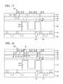
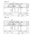
- FIGS. 20 to 27are sectional views of steps in a method of forming a semiconductor memory device, in accordance with a third embodiment of this invention.
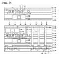
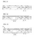
- FIGS. 28 to 37are sectional views of steps in a method of forming a semiconductor memory device, in accordance with a fourth embodiment of this invention.
- FIGS. 1 to 11illustrate a first embodiment of the semiconductor memory device in accordance with this invention.
- logic devicesare formed on a first semiconductor substrate 100 .
- the logic devicesare comprised of NMOS and PMOS transistors 110 , 112 , resistors (not illustrated) and interconnections (not illustrated).
- isolations 102are formed in the first semiconductor substrate 100 and define active region.
- the first semiconductor substrate 100can be bulk silicon, bulk silicon-germanium, or a semiconductor substrate on which silicon or silicon-germanium epitaxial layer is formed.
- the first semiconductor substrate 100can be Silicon-on-sapphire (SOS), silicon-on-insulator (SOI), thin film transistor (TFT), doped and undoped semiconductors, silicon epitaxial layer formed on the base semiconductor, or other semiconductor structures well known to those who are skilled in the art.
- the isolations 102can be formed by forming trenches on the first semiconductor substrate 100 , and then fill-in the trenches with dielectric materials such as High Density Plasma (HDP) oxide.
- dielectric materialssuch as High Density Plasma (HDP) oxide.
- well regionscan be formed in the first semiconductor substrate at pre-defined regions to form NMOS or PMOS transistors.
- the well regionscan be formed by ion implanting dopants into the surface of the first semiconductor substrate 100 .
- gate electrodes 110are formed on the first semiconductor substrate 100 by stacking and patterning gate dielectric film and gate conductor. After forming the gate conductors 110 , source/drain regions 112 are formed by ion-implanting dopants into each side of the gate electrodes 110 in the first semiconductor substrate 100 . This completes forming transistors on the first semiconductor substrate 100 .
- a first interlayer dielectric film 120is formed by depositing dielectric film with good step coverage. Resistors (not illustrated), diodes (not illustrated) and interconnections (not illustrated) can be included in the first interlayer dielectric film 120 .
- lower region storage devicesare formed on the first interlayer dielectric film 120 .
- the lower region storage devicescan be formed as capacitors.
- the storage devicescan be formed using phase change materials.
- the storage devicescan be formed with high-k material using its remnant polarization characteristics.
- the capacitorscan be shaped in various shapes such as stack type, pillar type, cylinder type.
- the stack type capacitorscan have first electrodes and second electrodes to be stacked face to face.
- the pillar type capacitorscan have pillar shaped first electrodes and the second electrodes are formed to surround the outer surface of the first electrodes conformal.
- the cylinder type capacitorscan have cylinder shaped first electrodes and the second electrodes are formed to cover the inner surface of the first electrodes conformal. In this embodiment of the invention, forming the cylinder type capacitors 132 , 134 will be explained.
- the first electrodes 132which are plate electrodes, are formed on the first interlayer dielectric film 120 in which the logic devices are included. That is, the pillar shaped first electrodes 132 are formed by depositing enough thickness of conducting film on the first interlayer dielectric film 120 and then performing photolithography and etch processes to the conducting film.
- the first electrodes 132After forming the first electrodes 132 , a dielectric film (not illustrated) and a conducting film for second electrodes are deposited conformal on the surface of the first electrodes 132 . As next steps, the second conducting film for the second electrodes is etched to separate the second conducting film into the second electrodes 134 .
- the second electrodes 134can be formed covering the first electrodes 132 pillars and the second electrodes 134 are separated from each others.
- the second electrodes 134are storage node electrodes, and can be formed as cylinder shaped which have open bottoms.
- the first and second electrodescan be formed with poly silicon or metal films, and the dielectric film (not illustrated) can be formed with Tantalum Oxide (Ta 2 O 5 ) or Aluminum Oxide (Al 2 O 3 ), or stacked films such as Tantalum Oxide/Titanium Oxide or Aluminum Oxide/Titanium Oxide.
- an insulating filmis deposited onto whole surface of the semiconductor substrate 100 .
- a planarization processsuch as CMP or etch back is performed to form a second interlayer dielectric film 140 , 150 .
- contact plugs 162 for lower region storage nodeswhich are individually connected to the second electrodes 134 and contact plugs 164 for logic which are individually connected to the transistors 110 , 112 .
- Conducting lines 174are formed on the contact plugs 162 , 164 .
- conducting lines which are not connected to the contact plugscan be also formed.
- These conducting lines which are not connected to the contact plugsare used as bit lines 172 which will be connected to the switching devices at the latter process steps. That is, on the top regions of the capacitors 132 , 134 , bit lines 172 and conducting lines 174 can be formed side by side.
- a third interlayer dielectric film 180is formed to cover the bit lines 172 and conducting lines 174 , and then contact plugs 182 to which are electrically connected to the bit lines 172 and the second electrodes 134 respectively, are formed in the third interlayer dielectric film 180 .
- a bonding layer 190is formed on top of the third interlayer dielectric film 180 which is at most upper layer of the first semiconductor substrate 100 .
- the bonding layerwill be used to bond a second semiconductor substrate 200 in where switching devices will be formed.
- the bonding layer 190can be formed with, for example, photo-setting adhesive such as reaction-setting adhesive, thermal-setting adhesive, photo-setting adhesive such as UV-setting adhesive, or anaerobe adhesive. Further, the bonding layer can be, such as, metallic bonds (Ti, TiN, Al), epoxy, acrylate, or silicon adhesives.
- the metallic materialcan be formed with material that has lower melting point than those of conducting materials used for contact plugs 162 , 164 and conducting lines 172 , 174 .
- the bonding layer 190can be formed with materials that can be re-flowed at a lower temperature planarization process so that it can prevent formation of voids between the second semiconductor substrate 200 and the bonding layer 190 .
- the bonding layer 190can increase the bonding strength when bonding the second semiconductor 200 onto the bonding layer 190 , and also decrease micro defects during the bonding process.
- the second semiconductor substrate 200is bonded onto the bonding layer 190 .
- the second semiconductor substrate 200can be a single crystalline semiconductor substrate which includes multiple doped layers 201 , 203 , 205 which are included in pre-defined depths from the surface of the second semiconductor substrate 200 .
- the multiple doped layers 201 , 203 , 205can be formed by ion-implanting dopants into the single crystalline semiconductor substrate, or adding dopants during an epitaxial process to form a single crystalline semiconductor substrate.
- the multiple doped layers 200can be formed to have n-type doped layers 201 , 205 and p-type doped layers 203 are arranged alternatively.
- NMOS transistorsare formed as a upper region switching devices so that n-type doped layer 201 , among the multiple doped layers 201 , 203 , 205 , is interfaced to the bonding layer 190 .
- the second semiconductor substrate 200includes a detaching layer 207 at the interface of the multiple doped layers 201 , 230 , 205 and the second single crystalline semiconductor substrate.
- the detaching layercan be porous layer, oxide film, nitride film, organic bonding film, or strained layer such as Si—Ge interface.
- Hydrogen Exfoliating ImplantThis method has a critical disadvantage which can destroy lattice structures of the substrate because it uses high amount of ion implantation. In order to recover the destroyed lattice structures, the substrate should be cured by heat treatment in very high temperature long time. This kind of high temperature heat treatment can damage cell devices in the lower regions.
- the detaching layer 207can be used to prevent multiple doped layers 201 , 203 , 205 not to be removed when removing single crystalline semiconductor substrate after bonding.
- the detaching layeralso helps to precisely and easily detach the single crystalline semiconductor substrate while remaining the multiple doped layers 201 , 203 , 205 .
- the second semiconductor substrate 200is bonded to the surface of the multiple doped layers 201 , 203 , 205 to be face to face to the bonding layer 190 .
- the substratescan be treated in a pre-defined pressure and temperature to increase bonding strength.
- the surface of the single crystalline semiconductor substrate 200is grinded, polished, or etched until the detaching layer 207 is exposed.
- anisotropic or isotropic etch processis performed to expose the multiple doped layers 201 , 203 , 205 . That is, n-type doped layer 205 is exposed.
- Exposing the multiple doped layers 200can be possible because the multiple doped layers 201 , 203 , 205 and detaching layer 207 are formed with different film material or formed with same material but with different film density. In other method, by adding physical shock to the detaching layer 207 , the detaching layer which has weak crystal lattice structure can be cracked to detaching the single crystalline semiconductor substrate 200 and the multiple doped layers 201 , 203 , 205 .
- n-type doped layer 201 , p-type doped layer 203 , and n-type doped layer 205can be formed orderly on the bonding layer 190 .
- pillar shaped semiconductor layer patterns 202 , 204 , 206are formed to form transistors with vertical channel structure.
- the pillar shaped semiconductor patterns 202 , 204 , 206are formed by patterning the multiple doped layers 201 , 203 , 205 .
- the semiconductor patterns 202 , 204 , 206can be formed by performing photolithography and etch processes to the multiple doped layers 201 , 203 , 205 . That is, n/p/n types of doped layers patterns can be formed.
- the bonding layercan be also etched. In this case, bonding layer patterns 190 can be formed under the pillar shaped semiconductor patterns 202 , and part of the surface of the third interlayer dielectric film can be exposed.
- gate electrodes 220are formed as spacer shape at each side of the semiconductor patterns 204 among the semiconductor patterns 202 , 204 , 206 .
- a fourth interlayer dielectric film 230is formed on the third interlayer dielectric film 180 to cover sidewalls of the semiconductor patterns 202 to which the bonding layer 190 is interfaced.
- contact plugs 206are formed to connect logic devices in the lower region and gate conductor 220 .
- gate dielectric and gate conductorare deposited conformal to the surface of the semiconductor patterns 204 , 206 on the fourth interlayer dielectric film 201 .
- the gate dielectric and gate conductorare anisotropic etched to form spacer shaped gate electrode 220 which surrounds the channel region (p-type semiconductor layer) of the pillar. This forms the vertical channel transistors.
- a fifth interlayer dielectric film 230is formed to cover the pillar shaped semiconductor patterns 202 , 204 , 206 and gate electrodes 220 .
- contact plugs 242are formed which are individually connected to the source/drain regions 206 in the fifth interlayer dielectric film 230 , and at the same time contact plugs 244 are formed which are connected to the logic devices.
- wirings 252 , 254are formed on the each of the contact plugs 242 , 244 .
- the wirings on the semiconductor patterns 202 , 204 , 206 which are connected to the capacitors 132 , 134are bit lines.
- a sixth interlayer dielectric film 260is formed after formation of wirings 252 , 254 , and then contact plugs for upper region storage nodes are selectively formed to be connected to the wirings 252 .
- Storage nodeswhich are contact plugs for the upper region storage nodes to be connected to the second electrode (that, is storage node electrodes) and source/drain regions 206 are formed on the semiconductor patterns 202 , 204 , 206 which are not connected to the lower regions capacitors 132 , 134 .
- upper region storage deviceswhich are upper region capacitors, are formed on the sixth interlayer dielectric film 260 .
- the upper region storage devicesare formed symmetrical to the lower region storage devices (capacitors 132 , 134 ), and can be electrically connected to the switching devices which are not connected to the lower region storage devices.
- the switching devices which are connected to the lower region storage devicescan be formed to be alternatively located to the switching devices which are connected to the upper regions storage devices.
- the upper regions storage devicescan be formed as cylinder type capacitors.
- a seventh interlayer dielectric film 270is formed in enough thickness on the sixth interlayer dielectric film 260 .
- the seventh interlayer dielectric film 270is then patterned and exposed to form openings on the top surface of the contact plugs 262 for the upper region storage nodes.
- conducting film for second electrodeare deposited conformal to the surface of the seventh interlayer dielectric film openings. And then, dielectric film (not illustrated) with good gap filling characteristics is deposited, and then the second electrode conductor film is planarized until the seventh interlayer dielectric film 270 is exposed. Then dielectric film (not illustrated) is formed conformal to the surface of the second electrodes 282 , and a first electrode conductor film is deposited to fill in the inside of the second electrode 282 . And then the first electrode film is patterned to form the first electrode 284 .
- an eighth interlayer dielectric film 280can be formed on the seventh interlayer dielectric film to cover the upper region storage devices 282 , 284 .
- contact plugs 292 and metal wirings 294can be formed to be connected to the logic devices.
- switching devices with vertical channelscan be formed by bonding semiconductor substrates on the logic devices, and the storage devices can be formed at upper and lower regions of the switching devices.
- FIGS. 12 to 19illustrates the steps in fabricating the semiconductor memory device of a second embodiment of this invention.
- logic devicesare formed on the first semiconductor substrate 100 .
- the logic devicescan be formed by forming NMOS and PMOS transistors 110 , 112 , resistors (not illustrated), diodes (not illustrated) and wirings (not illustrated).
- active regionscan be defined by forming isolations 102 in the first semiconductor substrate 100 . Then, gate dielectric and gate conductor film is stacked and patterned to form gate electrode in the active regions on the first semiconductor substrate 100 . After gate electrodes 110 are formed, dopants are ion-implanted at each side of the gate electrodes 110 to form source/drain regions 112 . This forms transistors on the first semiconductor substrate 100 .
- a first interlayer dielectric film 120is formed by depositing dielectric film with good step coverage on the transistors 110 , 112 .
- Resistors (not illustrated), diodes (not illustrated) and wirings (not illustrated)can be formed inside the first interlayer dielectric film 120 .
- lower regions storage devicesare formed on the first interlayer dielectric film 120 . Specifically, enough thickness of conducting film for the first electrode formation is deposited, and then the conductive film is exposed and etched to form pillar shaped first electrodes 132 . The first electrodes 132 which are biased with ground can be electrically connected each other.
- the second electrodes 134can be separated from each other while covering the first electrodes conformally.
- the second electrodes 134are storage node electrodes, and can have cylinder shapes with open bottoms.
- a second interlayer dielectric film 140 , 150is deposited all over the semiconductor substrate.
- the surface of the second interlayer dielectric film 140 , 150can be planarized by CMP or etch back processes, and contact plugs 162 and conducting pads 172 which are connected to the second electrode 134 .
- the lower region storage devices on the first interlayer dielectric film 120can be formed with refractory metals to reduce affect from the following high temperature process steps afterward.
- the refractory metalsare known to have low resistivity, low stress, good step coverage and good thermal expansion coefficient.
- the first and second electrodes 132 , 134 of the capacitors, contact plugs 162 and conducting pads 172can be formed with refractory metals.
- the refractory metalscan be, for example, Tungsten (W), Titanium (Ti), Molybdenum (Mo), Tantalum (Ta), Titanium Nitride (TiN), Tantalum Nitride (TaN), Zirconium Nitride (ZrN), or an alloy formed by combination of the Tungsten Nitride (TiN) and those other materials.
- the first and second electrodes 132 , 134 of the capacitorscan be formed with poly silicon film.
- a third interlayer dielectric film 180is deposited to cover the conducting pads 172 on the lower regions capacitors 132 , 134 , and the film 180 is planarized. Then a bonding layer 190 is formed on the third interlayer dielectric film 180 , and this bonding layer 190 is for bonding a second semiconductor substrate on the third interlayer dielectric film 180 .
- the bonding layer 190can be formed with, for example, photo-setting adhesive such as reaction-setting adhesive, thermal-setting adhesive, photo-setting adhesive such as UV-setting adhesive, or anaerobe adhesive. Further, the bonding layer can be, such as, metallic bonds (Ti, TiN, Al), epoxy, acrylate, or silicon adhesives.
- the metallic materialcan be formed with material that has lower melting point than those of conducting materials used for contact plugs 162 and conducting lines 172 .
- the bonding layer 190can be formed with materials that can be re-flowed at a lower temperature planarization process so that it can prevent formation of voids between the second semiconductor substrate 200 and the bonding layer 190 .
- the bonding layer 190can increase the bonding strength when bonding the second semiconductor 200 onto the bonding layer 190 , and also decrease micro defects during the bonding process.
- the second semiconductor substrate 200is bonded onto the bonding layer 190 .
- the second semiconductor substrate 200can be a single crystalline semiconductor substrate which includes doped layer 201 which is included in pre-defined depth from the surface of the second semiconductor substrate 200 .
- the doped layer 201can be formed by ion-implanting dopants into the single crystalline semiconductor substrate, or adding dopants during an epitaxial process to form a single crystalline semiconductor substrate.
- the second semiconductor substrate 200includes a detaching layer 207 at the interface of the doped layer 201 and the second single crystalline semiconductor substrate.
- the detaching layercan be porous layer, oxide film, nitride film, organic bonding film, or strained layer such as Si—Ge interface.
- bonding layer 209can be formed on the doped layer 201 .
- the surface of the single crystalline semiconductor substrate 200is grinded, polished, or etched until the detaching layer 207 is exposed.
- anisotropic or isotropic etch processis performed to expose the surface of the doped layer 201 .
- Exposing the doped layer 201can be possible because the doped layer 201 and detaching layer 207 are formed with different film material or formed with same material but with different film density. In other method, by adding physical shock to the detaching layer 207 , the detaching layer which has weak crystal lattice structure can be cracked to detaching the single crystalline semiconductor substrate 200 and the doped layer 201 .
- transistors with horizontal channelscan be formed on the bonded single crystalline semiconductor layer 201 .
- active regionsare defined by forming isolations 202 in the boded single crystalline semiconductor doped layer 201 . Then, gate dielectric film and gate conductor film are deposited and patterned on the single crystalline semiconductor doped layer 201 to form gate electrodes 210 .
- Source/drain regions 212 , 214are formed by doping the single crystalline semiconductor doped layer 201 at each side of the gate electrodes 210 .
- the neighboring gate electrodes 210can share common source regions 212 .
- Drain regions 214can be formed in the single crystalline semiconductor doped layer 201 near sidewall of the gate electrode 210 which apart (the other side) from the source regions 212 . Also, the certain drain regions 214 can be formed on the lower region capacitors 132 , 134 when forming the transistors.
- the source/drain regions 212 , 214 of each side of the gate electrode 210can be formed by ion-implantation and annealing process.
- the ion-implantation and annealing processcan be performed at temperatures of between about 800° C. (degrees Celsius) to about 850° C.
- the lower regions storage devices which are formed with refractory metalscan be prevented from decreasing reliability by the high temperature.
- a fourth interlayer dielectric film 220is formed to cover the transistors 210 , 212 , 214 formed on the second semiconductor substrate 200 . Then, contact holes 221 are formed by penetrating the fourth interlayer dielectric film 220 and the second semiconductor substrate 200 . The contact holes 221 expose the conducting lines 172 on the lower region capacitors 132 , 134 .
- dielectric filmis deposited along with the surface of the contact holes 221 , and then anisotropic etched to leave insulating spacer 222 on the inner wall of the contact holes 221 .
- the insulating spacer 222can prevent the bonding layer 190 , which is formed with conducting material, from exposed to other films or layers.
- contact plugs 224 for lower regions storage nodescan be formed by filling in the contact holes 221 with conducting material.
- the lower region storage nodescan be filled into the surface of the second semiconductor substrate 200 , and then electrically connected to the drain regions 214 in the second semiconductor substrate 200 .
- a fifth interlayer dielectric filmis formed on the fourth interlayer dielectric film, and the fifth interlayer dielectric film can fill in the contact holes.
- contact plugs 232 for bit lineare formed in the fourth and fifth interlayer dielectric films 220 , 230 .
- the contact plugs 232are connected to the common source regions 212 .
- contact plugs which are electrically connected to the logic devicescan be also formed.
- bit lines 234are formed on the contact plugs 232 for bit lines are formed perpendicular to the gate conductors. Also, conducting lines (not illustrated) which are connected to the logic devices can be formed when forming the bit lines 234 .
- a sixth interlayer dielectric film 240which covers the bit lines 234 are formed, and then contact plugs 242 for upper region storage nodes which are connected to the drain regions 214 are formed in the sixth interlayer dielectric films 240 .
- FIG. 19it is illustrated as the contact plugs 242 and bit lines 234 are piled up on each other, but in three dimensional view, the bit lines 234 and contact plugs for the storage nodes are electrically isolated.
- Open top cylinder shaped second electrodes 252can be formed on the contact plugs 242 for the upper storage nodes, as explained in the first embodiment of this invention. Then, a dielectric film (not illustrated) and the first electrode 254 can be formed on the second electrode 252 . The first electrode 254 can fill in the inside of the cylinder shaped second electrode 252 .
- an eighth interlayer dielectric film 270is formed to cover the upper region capacitors 252 , 254 , and contact plugs 282 which are connected to the logic devices 110 , 112 and final metal interconnections 292 are formed.
- FIGS. 20 to 27illustrate steps in a method of fabricating semiconductor memory device in accordance with a third embodiment of this invention.
- FIG. 20a first semiconductor substrate with logic device on it is provided.
- Transistors 110 , 112are formed on the first semiconductor substrate 100 , and then first interlayer dielectric film 120 is formed to cover the transistors 110 , 112 .
- Contact plugs 120are formed in the first interlayer dielectric film 120 , and wirings 122 are formed on the contact plugs.
- a second interlayer dielectric filmis formed to cover the wirings 122 , and then top of the second dielectric film is planarized.
- the logic devicesare formed on the first semiconductor substrate 100 , and then a bonding layer 140 is formed on the second interlayer dielectric film 130 .
- a second semiconductor substrate 200is provided.
- the second semiconductor substrate 200includes switching devices 210 , 212 , 214 and first storage devices 242 , 244 .
- the second semiconductor substrate 200can be a single crystalline semiconductor substrate which includes a doped layer in pre-defined depth.
- the single crystalline semiconductor substrateincludes doped layers of pre-defined depth from the surface.
- the single crystalline semiconductor substratealso includes a detaching layer 205 in a pre-defined depth to be interfaced with the doped layer.
- transistors 210 , 212 , 214 with horizontal channelsare formed on the second semiconductor substrate 200 as switching devices.
- a first interlayer dielectric filmis deposited to fill in the transistors 210 , 212 , 214 , and then bit line contact plugs 222 which are connected to the common source region 212 of the transistors are formed, and bit line 224 are formed as well step by step.
- a second interlayer dielectric film 230is formed to cover the bit lines, and contact plugs for storage nodes 232 are formed in the first and second interlayer dielectric films.
- capacitors 242 , 244are formed on each of the contact plugs 232 for storage nodes.
- a third interlayer dielectric film 240 with enough thicknessare formed on the second interlayer dielectric film 230 , and cylinder shaped storage nodes electrodes 242 are formed in the third interlayer dielectric film 240 .
- a dielectric film (not illustrated) and plate electrode 244are formed step by step on the storage node electrodes 242 .
- a fourth interlayer dielectric film 250are deposited to cover the capacitors 242 , 244 , and then a bonding layer 255 is formed on the fourth interlayer dielectric film.
- the first semiconductor substrate 100 and the second semiconductor substrate 200are bonded each other.
- the bonding layer 140 on the first semiconductor substrate 100 and the bonding layer 255 on the second semiconductor substrate 200are to be faced each other and bonded.
- the first storage devices 242 , 244 and switching devices 210 , 212 , 214are formed in this order.
- part of the backside of the second semiconductor substrate 200is removed.
- the removalcan be controlled by detaching layer which is formed inside the second semiconductor substrate 200 .
- contact plugs 208are formed in the second semiconductor substrate which are connected to the pre-defined drain regions of the transistors.
- second storage devices 262 , 264are formed on the backside of the second semiconductor substrate 200 .
- capacitors 262 , 264can be formed on the backside of the semiconductor substrate 200 , and the capacitors 262 , 262 are connected to the contact plugs 208 .
- open top cylinder shaped storage node electrodes 262are formed on the backside of the second semiconductor substrate 200 , then a dielectric film (not illustrated) and a plate electrode 264 are formed on the surface of the storage node electrodes 262 .
- contact plugs 272 , 274 , 276 and conducting lines 278are formed to be matched with bit lines 224 , gate electrodes 210 , and logic devices 110 , 112 .
- interlayer dielectric film 280is formed to cover the conducting lines 278 and a bonding layer 285 is formed on the interlayer dielectric film 280 .
- a third semiconductor substrateis provided.
- the third semiconductor substrateincludes switching devices 310 , 312 , 314 and third storage devices 342 , 344 .
- a bonding layer 355is formed on the third semiconductor substrate 300 , and then bonded to the bonding layer 285 of the second semiconductor substrate 200 . Forming the switching devices 310 , 312 and the third storage devices 342 , 344 on the third semiconductor substrate 300 will be practically same as forming switching devices 110 , 112 and the second storage devices 210 , 212 , 214 on the second semiconductor substrate 200 .
- FIG. 26illustrates removing part of the backside of the third semiconductor substrate 300 , and forming the fourth storage devices 362 , 364 which are electrically connected to the switching devices 310 , 312 .
- contact plugs for storage nodesare formed to be connected to the drain regions 314 of the transistors in the third semiconductor substrate 300 .
- capacitors 362 , 364are formed on the contact plugs for the storage nodes.
- the third storage devices 342 , 344are formed below the switching devices 310 , 312
- the fourth storage devices 362 , 364are formed above the switching devices 310 , 312 .
- contact plugs 372 , 374 and conducting lines 378are formed to be connected each to the bit lines 324 and gate electrodes 310 . Also, contact plugs 378 and conducting lines 378 formed to be connected to the logic devices 110 , 112 , 122 in the lower region. And then, final metal wirings 384 are formed on top of the contact plugs 378 .
- switching devices and storage devicescan be formed on the logic devices by bonding a semiconductor substrate with logic devices and another semiconductor substrate with switching and storage devices. Also, by repeating the bonding the semiconductor substrate with switching and storage devices, the chip density of the semiconductor memory device can be much improved.
- FIGS. 28 to 37are sectional views of the semiconductor memory device fabricated in accordance with this invention. It will be described with a fourth embodiment of this invention.
- a first semiconductor substrate 100is provided with a bonding layer 110 if formed on the surface.
- the first semiconductor substrate 100can be a dummy substrate with no doped layers or other devices are formed.
- a second semiconductor substrateis also provided.
- the second semiconductor substrateincludes switching devices 210 , 212 , 214 and first storage devices 242 , 244 .
- the second semiconductor substratealso includes a detaching layer 205 which will be used as etch stopper when removing part of the second semiconductor substrate in the following process steps. The same method can be used as explanation for the FIG. 21 when forming the switching devices 210 , 212 , 214 and the first storage devices 242 , 244 on the second semiconductor substrate 200 .
- a bonding layer 255is formed on the interlayer dielectric film 250 .
- the bonding layer 110 on the first semiconductor substrate 100 and the bonding layer 255 on the second semiconductor substrate 200are bonded each other face to face.
- the second semiconductor substrate 200are located on top of the first semiconductor substrate 100 , and the backside of the second semiconductor substrate 200 are now exposed to top.
- the storage devices 242 , 244 and the switching devices 210 , 212are arranged in this order. Then part of the top surface (which was backside of the second semiconductor substrate before bonding) of the second semiconductor substrate is removed to the detaching layer 205 in the second semiconductor substrate.
- second storage devices 262 , 264are formed on the second semiconductor substrate 200 .
- storage node contact plugs 208are formed to be contacted to the drain regions 214 in the second semiconductor substrate 200 .
- capacitors 242 , 244are formed on the storage node contact plugs 208 .
- bit lines 224 and contact plugswhich are connected to the gate electrodes 210 and wirings 278 can be formed.
- contact plugs 120are formed to be connected from the first semiconductor substrate 100 to the wirings 278 by following process steps. This completes formation of a first semiconductor device.
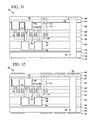
- a second semiconductor devicewhich has bonding layers on the backside and top most layer of the first semiconductor substrate 100 .
- the process steps and method for providing the second semiconductor deviceis practically same as providing the first semiconductor device. The only differences are, the second semiconductor device can have bonding layers 130 , 290 on the top surface of the first storage devices 242 , 244 and backside of the dummy semiconductor substrate 100 .
- a third semiconductor substrate 300is provided.
- Transistors 310 , 312 and wirings 322can be formed on the third semiconductor substrate 300 .
- contact plugs 340are formed.
- the contact plugs 340are connected from the backside of the third semiconductor substrate 300 to the wirings 322 on the third semiconductor substrate 300 .
- the contact plugs 340can be formed by penetrating the third semiconductor substrate 300 .
- Wirings 350can be formed on the backside of the third semiconductor substrate 300 which are electrically connected to the logic devices 310 , 312 .
- a bonding layer 360is formed on top of the third semiconductor substrate 300 .
- This bonding layer 360is to bond other semiconductor devices ( 10 , 20 of the FIG. 31 ) on top of the third semiconductor substrate 300 .
- the bonding layer 360can be formed with conducting materials, and this allows electrical connection between logic devices 310 , 312 and other semiconductor devices ( 10 , 20 of the FIG. 31 ). This completes providing the third semiconductor device 30 which includes logic devices 310 , 312 .
- the second semiconductor device 20which includes the third and fourth storage devices 242 , 244 , 262 , 264 and switching devices 210 , 212 , 214 , is bonded to the third semiconductor device 30 which includes logic devices 310 , 312 .
- the first semiconductor device 10which includes the first and second storage devices 242 , 244 , 262 , 264 and the switching devices 210 , 212 , is bonded to the second semiconductor device 20 .
- FIG. 37illustrates completed semiconductor memory device with repeated storage devices and switching devices formed on the logic devices 310 , 312 .
- the first to third semiconductor devicescan be electrically connected through bonding layers 130 , 290 which are formed with conducting material.
Landscapes
- Engineering & Computer Science (AREA)
- Manufacturing & Machinery (AREA)
- Physics & Mathematics (AREA)
- Condensed Matter Physics & Semiconductors (AREA)
- General Physics & Mathematics (AREA)
- Computer Hardware Design (AREA)
- Microelectronics & Electronic Packaging (AREA)
- Power Engineering (AREA)
- Semiconductor Memories (AREA)
Abstract
Description
- 1. Field of the Invention
- This invention relates to method for fabricating semiconductor memory device, more specifically relates to a method for fabricating three-dimensional semiconductor memory device to increase chip density.
- 2. Description of the Related Art
- Along with the advance in semiconductor manufacturing technology, a requirement for smaller pattern size and shorter distance between patterns on the chip. Using the smaller pattern size induces problems like high leakage currents. This is one of the reasons which limits increasing chip density by decreasing pattern size.
- In order to achieve high density semiconductor devices, recent developments focus on stacking semiconductor device on the substrate in three-dimensional structure.
- The present invention employs a method of fabricating three-dimensional semiconductor memory device which has vertically structured electrical devices by substrates bonding.
- The method of forming a three-dimensional structure semiconductor memory device is comprised of, forming first storage devices on the first semiconductor substrate; forming switching devices on the first storage devices; and forming second storage devices on the switching devices.
- In another embodiment, the method of fabricating semiconductor memory device according to this invention is comprised of, forming switching devices on the first semiconductor substrate; forming first storage devices on the switching devices which is electrically connected to the switching devices; and forming second storage devices on the backside of the first semiconductor substrate which are electrically connected to the switching devices.
FIGS. 1 to 11 are sectional views of steps in a method of forming a semiconductor memory device, in accordance with a first embodiment this invention.FIGS. 12 to 19 are sectional views of steps in a method of forming a semiconductor memory device, in accordance with a second embodiment of this invention.FIGS. 20 to 27 are sectional views of steps in a method of forming a semiconductor memory device, in accordance with a third embodiment of this invention.FIGS. 28 to 37 are sectional views of steps in a method of forming a semiconductor memory device, in accordance with a fourth embodiment of this invention.FIGS. 1 to 11 illustrate a first embodiment of the semiconductor memory device in accordance with this invention.- In
FIG. 1 , logic devices are formed on afirst semiconductor substrate 100. The logic devices are comprised of NMOS andPMOS transistors - More specifically,
isolations 102 are formed in thefirst semiconductor substrate 100 and define active region. Thefirst semiconductor substrate 100 can be bulk silicon, bulk silicon-germanium, or a semiconductor substrate on which silicon or silicon-germanium epitaxial layer is formed. Also, thefirst semiconductor substrate 100 can be Silicon-on-sapphire (SOS), silicon-on-insulator (SOI), thin film transistor (TFT), doped and undoped semiconductors, silicon epitaxial layer formed on the base semiconductor, or other semiconductor structures well known to those who are skilled in the art. - The
isolations 102 can be formed by forming trenches on thefirst semiconductor substrate 100, and then fill-in the trenches with dielectric materials such as High Density Plasma (HDP) oxide. - Before forming the
isolations 102, well regions can be formed in the first semiconductor substrate at pre-defined regions to form NMOS or PMOS transistors. The well regions can be formed by ion implanting dopants into the surface of thefirst semiconductor substrate 100. - After defining the well regions in the
first semiconductor substrate 100,gate electrodes 110 are formed on thefirst semiconductor substrate 100 by stacking and patterning gate dielectric film and gate conductor. After forming thegate conductors 110, source/drain regions 112 are formed by ion-implanting dopants into each side of thegate electrodes 110 in thefirst semiconductor substrate 100. This completes forming transistors on thefirst semiconductor substrate 100. - In
FIG. 2 , a first interlayerdielectric film 120 is formed by depositing dielectric film with good step coverage. Resistors (not illustrated), diodes (not illustrated) and interconnections (not illustrated) can be included in the first interlayerdielectric film 120. - As following steps, lower region storage devices are formed on the first interlayer
dielectric film 120. In this embodiment of this invention, the lower region storage devices can be formed as capacitors. In another embodiment, the storage devices can be formed using phase change materials. In the other embodiment, the storage devices can be formed with high-k material using its remnant polarization characteristics. - When capacitors are used to form the storage devices, the capacitors can be shaped in various shapes such as stack type, pillar type, cylinder type. The stack type capacitors can have first electrodes and second electrodes to be stacked face to face. The pillar type capacitors can have pillar shaped first electrodes and the second electrodes are formed to surround the outer surface of the first electrodes conformal. And the cylinder type capacitors can have cylinder shaped first electrodes and the second electrodes are formed to cover the inner surface of the first electrodes conformal. In this embodiment of the invention, forming the
cylinder type capacitors - More specifically, the
first electrodes 132, which are plate electrodes, are formed on the first interlayerdielectric film 120 in which the logic devices are included. That is, the pillar shapedfirst electrodes 132 are formed by depositing enough thickness of conducting film on the first interlayerdielectric film 120 and then performing photolithography and etch processes to the conducting film. - After forming the
first electrodes 132, a dielectric film (not illustrated) and a conducting film for second electrodes are deposited conformal on the surface of thefirst electrodes 132. As next steps, the second conducting film for the second electrodes is etched to separate the second conducting film into thesecond electrodes 134. In other words, thesecond electrodes 134 can be formed covering thefirst electrodes 132 pillars and thesecond electrodes 134 are separated from each others. Thesecond electrodes 134 are storage node electrodes, and can be formed as cylinder shaped which have open bottoms. - When forming the cylinder type
lower region capacitors - In
FIG. 3 , after formingcapacitors semiconductor substrate 100. As a following step, a planarization process such as CMP or etch back is performed to form a second interlayerdielectric film - As following steps, contact
plugs 162 for lower region storage nodes which are individually connected to thesecond electrodes 134 and contactplugs 164 for logic which are individually connected to thetransistors lines 174 are formed on thecontact plugs bit lines 172 which will be connected to the switching devices at the latter process steps. That is, on the top regions of thecapacitors bit lines 172 and conductinglines 174 can be formed side by side. - A third interlayer
dielectric film 180 is formed to cover thebit lines 172 and conductinglines 174, and then contactplugs 182 to which are electrically connected to thebit lines 172 and thesecond electrodes 134 respectively, are formed in the third interlayerdielectric film 180. - In
FIG. 4 , abonding layer 190 is formed on top of the third interlayerdielectric film 180 which is at most upper layer of thefirst semiconductor substrate 100. The bonding layer will be used to bond asecond semiconductor substrate 200 in where switching devices will be formed. - The
bonding layer 190 can be formed with, for example, photo-setting adhesive such as reaction-setting adhesive, thermal-setting adhesive, photo-setting adhesive such as UV-setting adhesive, or anaerobe adhesive. Further, the bonding layer can be, such as, metallic bonds (Ti, TiN, Al), epoxy, acrylate, or silicon adhesives. - When the
bonding layer 190 is formed with metallic materials, the metallic material can be formed with material that has lower melting point than those of conducting materials used forcontact plugs lines bonding layer 190 can be formed with materials that can be re-flowed at a lower temperature planarization process so that it can prevent formation of voids between thesecond semiconductor substrate 200 and thebonding layer 190. Thebonding layer 190 can increase the bonding strength when bonding thesecond semiconductor 200 onto thebonding layer 190, and also decrease micro defects during the bonding process. - As a following step, the
second semiconductor substrate 200 is bonded onto thebonding layer 190. Specifically, thesecond semiconductor substrate 200 can be a single crystalline semiconductor substrate which includes multiple dopedlayers second semiconductor substrate 200. The multiple dopedlayers - The multiple doped
layers 200 can be formed to have n-type dopedlayers layers 203 are arranged alternatively. In this embodiment of this invention, NMOS transistors are formed as a upper region switching devices so that n-type dopedlayer 201, among the multiple dopedlayers bonding layer 190. - Also, the
second semiconductor substrate 200 includes adetaching layer 207 at the interface of the multiple dopedlayers - Among the technologies to form the detaching layer, one of the well known technologies is Hydrogen Exfoliating Implant. This method has a critical disadvantage which can destroy lattice structures of the substrate because it uses high amount of ion implantation. In order to recover the destroyed lattice structures, the substrate should be cured by heat treatment in very high temperature long time. This kind of high temperature heat treatment can damage cell devices in the lower regions.
- The
detaching layer 207 can be used to prevent multiple dopedlayers layers - In
FIG. 5 , thesecond semiconductor substrate 200 is bonded to the surface of the multiple dopedlayers bonding layer 190. After bonding, the substrates can be treated in a pre-defined pressure and temperature to increase bonding strength. - When bonding the
second semiconductor substrate 200 onto the bonding layer, no precise alignment is required because there are no patterns yet formed on thesecond semiconductor substrate 200. - After bonding the
second semiconductor substrate 200 onto thebonding layer 190, all regions of thesecond semiconductor substrate 200 are removed while only remaining the multiple dopedlayers 200. As a result, only the multiple dopedlayers bonding layer 190. - More specifically, after bonding, the surface of the single
crystalline semiconductor substrate 200 is grinded, polished, or etched until thedetaching layer 207 is exposed. After thedetaching layer 207 is exposed, anisotropic or isotropic etch process is performed to expose the multiple dopedlayers layer 205 is exposed. - Exposing the multiple doped
layers 200 can be possible because the multiple dopedlayers layer 207 are formed with different film material or formed with same material but with different film density. In other method, by adding physical shock to thedetaching layer 207, the detaching layer which has weak crystal lattice structure can be cracked to detaching the singlecrystalline semiconductor substrate 200 and the multiple dopedlayers - As a result, n-type doped
layer 201, p-type dopedlayer 203, and n-type dopedlayer 205 can be formed orderly on thebonding layer 190. - In
FIG. 6 , pillar shapedsemiconductor layer patterns semiconductor patterns layers - More specifically, the
semiconductor patterns layers semiconductor patterns bonding layer patterns 190 can be formed under the pillar shapedsemiconductor patterns 202, and part of the surface of the third interlayer dielectric film can be exposed. - In
FIG. 7 ,gate electrodes 220 are formed as spacer shape at each side of thesemiconductor patterns 204 among thesemiconductor patterns - More specifically, a fourth
interlayer dielectric film 230 is formed on the thirdinterlayer dielectric film 180 to cover sidewalls of thesemiconductor patterns 202 to which thebonding layer 190 is interfaced. As following steps, in the third and fourth interlayerdielectric films gate conductor 220. And then, gate dielectric and gate conductor are deposited conformal to the surface of thesemiconductor patterns interlayer dielectric film 201. The gate dielectric and gate conductor are anisotropic etched to form spacer shapedgate electrode 220 which surrounds the channel region (p-type semiconductor layer) of the pillar. This forms the vertical channel transistors. - In
FIG. 8 , a fifthinterlayer dielectric film 230 is formed to cover the pillar shapedsemiconductor patterns gate electrodes 220. After this step, contact plugs242 are formed which are individually connected to the source/drain regions 206 in the fifthinterlayer dielectric film 230, and at the same time contact plugs244 are formed which are connected to the logic devices. And then wirings252,254 are formed on the each of the contact plugs242,244. Among the wirings, the wirings on thesemiconductor patterns capacitors - In
FIG. 9 , a sixthinterlayer dielectric film 260 is formed after formation ofwirings wirings 252. - Storage nodes which are contact plugs for the upper region storage nodes to be connected to the second electrode (that, is storage node electrodes) and source/
drain regions 206 are formed on thesemiconductor patterns lower regions capacitors - As following steps, upper region storage devices, which are upper region capacitors, are formed on the sixth
interlayer dielectric film 260. The upper region storage devices (capacitors) are formed symmetrical to the lower region storage devices (capacitors 132,134), and can be electrically connected to the switching devices which are not connected to the lower region storage devices. Also, the switching devices which are connected to the lower region storage devices can be formed to be alternatively located to the switching devices which are connected to the upper regions storage devices. In this embodiment of the invention, the upper regions storage devices can be formed as cylinder type capacitors. - More specifically, a seventh
interlayer dielectric film 270 is formed in enough thickness on the sixthinterlayer dielectric film 260. The seventhinterlayer dielectric film 270 is then patterned and exposed to form openings on the top surface of the contact plugs262 for the upper region storage nodes. - In
FIG. 10 , conducting film for second electrode are deposited conformal to the surface of the seventh interlayer dielectric film openings. And then, dielectric film (not illustrated) with good gap filling characteristics is deposited, and then the second electrode conductor film is planarized until the seventhinterlayer dielectric film 270 is exposed. Then dielectric film (not illustrated) is formed conformal to the surface of thesecond electrodes 282, and a first electrode conductor film is deposited to fill in the inside of thesecond electrode 282. And then the first electrode film is patterned to form thefirst electrode 284. - In
FIG. 11 , an eighthinterlayer dielectric film 280 can be formed on the seventh interlayer dielectric film to cover the upperregion storage devices metal wirings 294 can be formed to be connected to the logic devices. - In accordance with the first embodiment of this invention, switching devices with vertical channels can be formed by bonding semiconductor substrates on the logic devices, and the storage devices can be formed at upper and lower regions of the switching devices.
- The
FIGS. 12 to 19 illustrates the steps in fabricating the semiconductor memory device of a second embodiment of this invention. - In
FIG. 12 , logic devices are formed on thefirst semiconductor substrate 100. The logic devices can be formed by forming NMOS andPMOS transistors - More specifically, active regions can be defined by forming
isolations 102 in thefirst semiconductor substrate 100. Then, gate dielectric and gate conductor film is stacked and patterned to form gate electrode in the active regions on thefirst semiconductor substrate 100. Aftergate electrodes 110 are formed, dopants are ion-implanted at each side of thegate electrodes 110 to form source/drain regions 112. This forms transistors on thefirst semiconductor substrate 100. - Then, a first
interlayer dielectric film 120 is formed by depositing dielectric film with good step coverage on thetransistors interlayer dielectric film 120. - In
FIG. 13 , lower regions storage devices are formed on the firstinterlayer dielectric film 120. Specifically, enough thickness of conducting film for the first electrode formation is deposited, and then the conductive film is exposed and etched to form pillar shapedfirst electrodes 132. Thefirst electrodes 132 which are biased with ground can be electrically connected each other. - After forming the
first electrodes 132, a dielectric film (not illustrated) and a conducting film for second electrode is deposited conformal to the surface of thefirst electrode 132. The second conductive film for second electrode is then etched to be separated assecond electrodes 134. By this process, thesecond electrodes 134 can be separated from each other while covering the first electrodes conformally. In this case, thesecond electrodes 134 are storage node electrodes, and can have cylinder shapes with open bottoms. - After forming the
capacitors interlayer dielectric film interlayer dielectric film pads 172 which are connected to thesecond electrode 134. - The lower region storage devices on the first
interlayer dielectric film 120 can be formed with refractory metals to reduce affect from the following high temperature process steps afterward. The refractory metals are known to have low resistivity, low stress, good step coverage and good thermal expansion coefficient. The first andsecond electrodes pads 172 can be formed with refractory metals. The refractory metals can be, for example, Tungsten (W), Titanium (Ti), Molybdenum (Mo), Tantalum (Ta), Titanium Nitride (TiN), Tantalum Nitride (TaN), Zirconium Nitride (ZrN), or an alloy formed by combination of the Tungsten Nitride (TiN) and those other materials. Also, the first andsecond electrodes - In
FIG. 14 , a thirdinterlayer dielectric film 180 is deposited to cover theconducting pads 172 on thelower regions capacitors film 180 is planarized. Then abonding layer 190 is formed on the thirdinterlayer dielectric film 180, and thisbonding layer 190 is for bonding a second semiconductor substrate on the thirdinterlayer dielectric film 180. - The
bonding layer 190 can be formed with, for example, photo-setting adhesive such as reaction-setting adhesive, thermal-setting adhesive, photo-setting adhesive such as UV-setting adhesive, or anaerobe adhesive. Further, the bonding layer can be, such as, metallic bonds (Ti, TiN, Al), epoxy, acrylate, or silicon adhesives. - When the
bonding layer 190 is formed with metallic materials, the metallic material can be formed with material that has lower melting point than those of conducting materials used for contact plugs162 and conductinglines 172. And, thebonding layer 190 can be formed with materials that can be re-flowed at a lower temperature planarization process so that it can prevent formation of voids between thesecond semiconductor substrate 200 and thebonding layer 190. Thebonding layer 190 can increase the bonding strength when bonding thesecond semiconductor 200 onto thebonding layer 190, and also decrease micro defects during the bonding process. - As a following step, the
second semiconductor substrate 200 is bonded onto thebonding layer 190. Specifically, thesecond semiconductor substrate 200 can be a single crystalline semiconductor substrate which includes dopedlayer 201 which is included in pre-defined depth from the surface of thesecond semiconductor substrate 200. The dopedlayer 201 can be formed by ion-implanting dopants into the single crystalline semiconductor substrate, or adding dopants during an epitaxial process to form a single crystalline semiconductor substrate. - Also, the
second semiconductor substrate 200 includes adetaching layer 207 at the interface of the dopedlayer 201 and the second single crystalline semiconductor substrate. The detaching layer can be porous layer, oxide film, nitride film, organic bonding film, or strained layer such as Si—Ge interface. Also,bonding layer 209 can be formed on the dopedlayer 201. - In
FIG. 15 , after completely bonding thesecond semiconductor substrate 200 on thebonding layer 190, all of thesecond semiconductor substrate 200 is removed only except the single crystalline semiconductor dopedlayer 201. As a result, single crystalline semiconductor dopedlayer 201 which has n-type or p-type dopants can be formed on thebonding layer 190 which is formed with metallic material. - More specifically, after bonding, the surface of the single
crystalline semiconductor substrate 200 is grinded, polished, or etched until thedetaching layer 207 is exposed. After thedetaching layer 207 is exposed, anisotropic or isotropic etch process is performed to expose the surface of the dopedlayer 201. - Exposing the doped
layer 201 can be possible because the dopedlayer 201 and detachinglayer 207 are formed with different film material or formed with same material but with different film density. In other method, by adding physical shock to thedetaching layer 207, the detaching layer which has weak crystal lattice structure can be cracked to detaching the singlecrystalline semiconductor substrate 200 and the dopedlayer 201. - As following steps, transistors with horizontal channels can be formed on the bonded single
crystalline semiconductor layer 201. - More specifically, active regions are defined by forming
isolations 202 in the boded single crystalline semiconductor dopedlayer 201. Then, gate dielectric film and gate conductor film are deposited and patterned on the single crystalline semiconductor dopedlayer 201 to formgate electrodes 210. Source/drain regions layer 201 at each side of thegate electrodes 210. The neighboringgate electrodes 210 can sharecommon source regions 212. Drainregions 214 can be formed in the single crystalline semiconductor dopedlayer 201 near sidewall of thegate electrode 210 which apart (the other side) from thesource regions 212. Also, thecertain drain regions 214 can be formed on thelower region capacitors - The source/
drain regions gate electrode 210 can be formed by ion-implantation and annealing process. The ion-implantation and annealing process can be performed at temperatures of between about 800° C. (degrees Celsius) to about 850° C. When the process is held a high temperature, the lower regions storage devices which are formed with refractory metals can be prevented from decreasing reliability by the high temperature. - In
FIG. 16 , a fourthinterlayer dielectric film 220 is formed to cover thetransistors second semiconductor substrate 200. Then, contactholes 221 are formed by penetrating the fourthinterlayer dielectric film 220 and thesecond semiconductor substrate 200. The contact holes221 expose the conductinglines 172 on thelower region capacitors - After forming the contact holes221, dielectric film is deposited along with the surface of the contact holes221, and then anisotropic etched to leave insulating
spacer 222 on the inner wall of the contact holes221. The insulatingspacer 222 can prevent thebonding layer 190, which is formed with conducting material, from exposed to other films or layers. - In
FIG. 17 , contact plugs224 for lower regions storage nodes can be formed by filling in the contact holes221 with conducting material. The lower region storage nodes can be filled into the surface of thesecond semiconductor substrate 200, and then electrically connected to thedrain regions 214 in thesecond semiconductor substrate 200. - In
FIG. 18 , a fifth interlayer dielectric film is formed on the fourth interlayer dielectric film, and the fifth interlayer dielectric film can fill in the contact holes. As a following step, contact plugs232 for bit line are formed in the fourth and fifth interlayerdielectric films common source regions 212. When forming the contact plugs121 for bit lines, contact plugs which are electrically connected to the logic devices can be also formed. In following steps,bit lines 234 are formed on the contact plugs232 for bit lines are formed perpendicular to the gate conductors. Also, conducting lines (not illustrated) which are connected to the logic devices can be formed when forming the bit lines234. - In
FIG. 19 , a sixthinterlayer dielectric film 240 which covers thebit lines 234 are formed, and then contact plugs242 for upper region storage nodes which are connected to thedrain regions 214 are formed in the sixth interlayerdielectric films 240. - In the
FIG. 19 , it is illustrated as the contact plugs242 andbit lines 234 are piled up on each other, but in three dimensional view, thebit lines 234 and contact plugs for the storage nodes are electrically isolated. - Open top cylinder shaped
second electrodes 252 can be formed on the contact plugs242 for the upper storage nodes, as explained in the first embodiment of this invention. Then, a dielectric film (not illustrated) and thefirst electrode 254 can be formed on thesecond electrode 252. Thefirst electrode 254 can fill in the inside of the cylinder shapedsecond electrode 252. - As following steps, an eighth
interlayer dielectric film 270 is formed to cover theupper region capacitors logic devices final metal interconnections 292 are formed. FIGS. 20 to 27 illustrate steps in a method of fabricating semiconductor memory device in accordance with a third embodiment of this invention.- In
FIG. 20 , a first semiconductor substrate with logic device on it is provided. Transistors first semiconductor substrate 100, and then firstinterlayer dielectric film 120 is formed to cover thetransistors interlayer dielectric film 120, and wirings122 are formed on the contact plugs. Then, a second interlayer dielectric film is formed to cover thewirings 122, and then top of the second dielectric film is planarized. The logic devices are formed on thefirst semiconductor substrate 100, and then abonding layer 140 is formed on the secondinterlayer dielectric film 130.- In
FIG. 21 , asecond semiconductor substrate 200 is provided. Thesecond semiconductor substrate 200 includes switchingdevices first storage devices second semiconductor substrate 200 can be a single crystalline semiconductor substrate which includes a doped layer in pre-defined depth. The single crystalline semiconductor substrate includes doped layers of pre-defined depth from the surface. The single crystalline semiconductor substrate also includes adetaching layer 205 in a pre-defined depth to be interfaced with the doped layer. - As following steps,
transistors second semiconductor substrate 200 as switching devices. After forming the transistors, a first interlayer dielectric film is deposited to fill in thetransistors common source region 212 of the transistors are formed, and bitline 224 are formed as well step by step. A secondinterlayer dielectric film 230 is formed to cover the bit lines, and contact plugs forstorage nodes 232 are formed in the first and second interlayer dielectric films. Then,capacitors interlayer dielectric film 240 with enough thickness are formed on the secondinterlayer dielectric film 230, and cylinder shapedstorage nodes electrodes 242 are formed in the thirdinterlayer dielectric film 240. A dielectric film (not illustrated) andplate electrode 244 are formed step by step on thestorage node electrodes 242. Then, a fourthinterlayer dielectric film 250 are deposited to cover thecapacitors bonding layer 255 is formed on the fourth interlayer dielectric film. - In
FIG. 22 , thefirst semiconductor substrate 100 and thesecond semiconductor substrate 200 are bonded each other. - Specifically, the
bonding layer 140 on thefirst semiconductor substrate 100 and thebonding layer 255 on thesecond semiconductor substrate 200 are to be faced each other and bonded. As a result, on thelogic devices first storage devices devices - In
FIG. 23 , part of the backside of thesecond semiconductor substrate 200 is removed. The removal can be controlled by detaching layer which is formed inside thesecond semiconductor substrate 200. - Then, contact plugs208 are formed in the second semiconductor substrate which are connected to the pre-defined drain regions of the transistors.
- In
FIG. 24 ,second storage devices second semiconductor substrate 200. Specifically,capacitors semiconductor substrate 200, and thecapacitors storage node electrodes 262 are formed on the backside of thesecond semiconductor substrate 200, then a dielectric film (not illustrated) and aplate electrode 264 are formed on the surface of thestorage node electrodes 262. - After forming the
capacitors lines 278 are formed to be matched withbit lines 224,gate electrodes 210, andlogic devices - Then,
interlayer dielectric film 280 is formed to cover the conductinglines 278 and abonding layer 285 is formed on theinterlayer dielectric film 280. - In
FIG. 25 , a third semiconductor substrate is provided. The third semiconductor substrate includes switchingdevices third storage devices bonding layer 355 is formed on thethird semiconductor substrate 300, and then bonded to thebonding layer 285 of thesecond semiconductor substrate 200. Forming theswitching devices third storage devices third semiconductor substrate 300 will be practically same as formingswitching devices second storage devices second semiconductor substrate 200. FIG. 26 illustrates removing part of the backside of thethird semiconductor substrate 300, and forming thefourth storage devices switching devices - Then, contact plugs for storage nodes are formed to be connected to the
drain regions 314 of the transistors in thethird semiconductor substrate 300. After this,capacitors third storage devices devices fourth storage devices devices - In
FIG. 27 , contact plugs372,374 and conducting lines378 are formed to be connected each to thebit lines 324 andgate electrodes 310. Also, contact plugs378 and conducting lines378 formed to be connected to thelogic devices final metal wirings 384 are formed on top of the contact plugs378. - As described in this embodiment, switching devices and storage devices can be formed on the logic devices by bonding a semiconductor substrate with logic devices and another semiconductor substrate with switching and storage devices. Also, by repeating the bonding the semiconductor substrate with switching and storage devices, the chip density of the semiconductor memory device can be much improved.
FIGS. 28 to 37 are sectional views of the semiconductor memory device fabricated in accordance with this invention. It will be described with a fourth embodiment of this invention.- In
FIG. 28 , afirst semiconductor substrate 100 is provided with abonding layer 110 if formed on the surface. Thefirst semiconductor substrate 100 can be a dummy substrate with no doped layers or other devices are formed. - A second semiconductor substrate is also provided. The second semiconductor substrate includes switching
devices first storage devices detaching layer 205 which will be used as etch stopper when removing part of the second semiconductor substrate in the following process steps. The same method can be used as explanation for theFIG. 21 when forming theswitching devices first storage devices second semiconductor substrate 200. After forming theinterlayer dielectric film 250 which covers thefirst storage devices bonding layer 255 is formed on theinterlayer dielectric film 250. - Then, the
bonding layer 110 on thefirst semiconductor substrate 100 and thebonding layer 255 on thesecond semiconductor substrate 200 are bonded each other face to face. As a result, thesecond semiconductor substrate 200 are located on top of thefirst semiconductor substrate 100, and the backside of thesecond semiconductor substrate 200 are now exposed to top. - In
FIG. 29 , as a result of bonding, thestorage devices switching devices detaching layer 205 in the second semiconductor substrate. - In
FIG. 30 ,second storage devices second semiconductor substrate 200. Specifically, storage node contact plugs208 are formed to be contacted to thedrain regions 214 in thesecond semiconductor substrate 200. Then,capacitors lines 224 and contact plugs which are connected to thegate electrodes 210 andwirings 278 can be formed. - In
FIG. 31 , contact plugs120 are formed to be connected from thefirst semiconductor substrate 100 to thewirings 278 by following process steps. This completes formation of a first semiconductor device. - In
FIG. 32 , a second semiconductor device is provided which has bonding layers on the backside and top most layer of thefirst semiconductor substrate 100. The process steps and method for providing the second semiconductor device is practically same as providing the first semiconductor device. The only differences are, the second semiconductor device can havebonding layers first storage devices dummy semiconductor substrate 100. - In
FIG. 33 , athird semiconductor substrate 300 is provided.Transistors wirings 322 can be formed on thethird semiconductor substrate 300. - As illustrated in
FIG. 34 , contact plugs340 are formed. The contact plugs340 are connected from the backside of thethird semiconductor substrate 300 to thewirings 322 on thethird semiconductor substrate 300. The contact plugs340 can be formed by penetrating thethird semiconductor substrate 300.Wirings 350 can be formed on the backside of thethird semiconductor substrate 300 which are electrically connected to thelogic devices - In
FIG. 35 , abonding layer 360 is formed on top of thethird semiconductor substrate 300. Thisbonding layer 360 is to bond other semiconductor devices (10,20 of theFIG. 31 ) on top of thethird semiconductor substrate 300. Thebonding layer 360 can be formed with conducting materials, and this allows electrical connection betweenlogic devices FIG. 31 ). This completes providing thethird semiconductor device 30 which includeslogic devices - In
FIG. 36 , thesecond semiconductor device 20, which includes the third andfourth storage devices devices third semiconductor device 30 which includeslogic devices first semiconductor device 10, which includes the first andsecond storage devices switching devices second semiconductor device 20. FIG. 37 illustrates completed semiconductor memory device with repeated storage devices and switching devices formed on thelogic devices bonding layers - The embodiments of the invention described herein are exemplary and numerous modifications, variations and rearrangements can be readily envisioned to achieve substantially equivalent results, all of which are intended to be embraced within the spirit and scope of the invention.
Claims (20)
1. A method for fabricating semiconductor memory device, comprising:
providing a first semiconductor substrate;
forming a first storage device on the first semiconductor substrate;
forming a switching device on the first storage device; and
forming a second storage devices on the switching device.
2. The method ofclaim 1 , wherein logic devices are formed below the first storage devices to be electrically connected to the switching devices.
3. The method ofclaim 1 , wherein forming the first or the second storage devices includes, forming first electrodes which is connected to the switching devices; forming a dielectric film on the first electrode; and forming second electrodes on the dielectric film.
4. The method ofclaim 3 , wherein the dielectric film is formed with dielectric film, high-k dielectric film, or phase change film.
5. The method ofclaim 1 , wherein forming the first and second storage devices includes, forming pillar shaped first electrodes which are connected to the switching devices; forming a dielectric film on surface of the first electrodes conformal; and forming second electrodes on surface of the dielectric film conformal.
6. The method ofclaim 1 , wherein forming the first and second storage devices includes, forming cylinder shaped first electrodes which are connected to the switching devices; forming a dielectric film on surface of the first electrodes conformal; and forming second electrodes on surface of the dielectric film conformal to fill up the inside of the cylinder shaped first electrodes.
7. The method ofclaim 1 , wherein forming the switching devices includes, bonding a second semiconductor substrate on the first storage devices; and forming second switching devices on the second semiconductor substrate.
8. The method ofclaim 7 , wherein forming the switching devices further includes before forming the switching devices, forming insulating layer which covers the first storage devices; and bonding the second semiconductor substrate on the insulating layer.
9. The method ofclaim 8 , wherein bonding the second semiconductor substrate is comprising of, providing a single crystalline semiconductor substrate; forming multiple doped layers which is uniformly formed in a pre-defined depth from the surface of the single crystalline semiconductor substrate; bonding the single crystalline semiconductor substrate to the top surface of the first insulating layer to face to face; and removing part of the single crystalline semiconductor substrate until the surface of the doped layers are exposed.
10. The method ofclaim 9 , wherein further forming a detaching layer in a pre-defined depth to be contacted to the multiple doped layers in the single crystalline semiconductor substrate, after forming the multiple doped layers.
11. The method ofclaim 10 , wherein forming the detaching layer is forming porous layer.
12. The method ofclaim 9 , wherein forming the multiple doped layers is forming p-type, n-type, p-type doped layers or forming n-type, p-type, n-type doped layers from the surface of the single crystalline semiconductor substrate.
13. The method ofclaim 9 , wherein the method further includes after bonding the second semiconductor substrate, forming doped layers patterns by patterning the multiple doped layers; and forming second storage devices on the surface of the doped layers patterns.
14. The method ofclaim 13 , wherein the multiple doped layers patterns include channel regions, and source regions and drain regions at the upper and lower side of the channel regions.
15. The method ofclaim 14 , wherein gate conductors are formed to complete the switching devices after forming the doped layers patterns to surround the channel regions.
16. The method ofclaim 8 , wherein bonding the second semiconductor substrate is comprising,
providing single crystalline semiconductor substrate which includes doped layers in which dopants are doped in pre-defined depth from the surface;
bonding the single crystalline semiconductor substrate to the top surface of the first insulating layer to face the surface of the doped layers; and
removing part of the single crystalline semiconductor substrate until the surface of the doped layers is exposed.
17. The method ofclaim 16 , wherein the single crystalline semiconductor substrate further includes a detaching layer which is formed at the pre-defined depth in where the doped layers is faced in the single crystalline semiconductor substrate.
18. The method ofclaim 16 , wherein forming the switching devices further includes forming gate electrodes on the second semiconductor substrate, and forming doped layers at each side of the gate electrodes.
19. The method ofclaim 18 , wherein forming the first storage devices includes forming wiring layers formed with metal or refractory metals.
20. The method ofclaim 19 , wherein the wiring layers are formed with Cobalt (Co), Titanium (Ti), Tungsten (W), Nickel (Ni), Platinum (Pt), Hafnium (Hf), Molybdenum (Mo), Palladium (Pd), Titanium Nitride (TiN), Tantalum Nitride (TaN), Zirconium Nitride (ZrN), Tungsten Nitride, or an alloy formed by combination of those metals.
Priority Applications (3)
| Application Number | Priority Date | Filing Date | Title |
|---|---|---|---|
| US12/635,496US20110143506A1 (en) | 2009-12-10 | 2009-12-10 | Method for fabricating a semiconductor memory device |
| US12/881,628US20110001172A1 (en) | 2005-03-29 | 2010-09-14 | Three-dimensional integrated circuit structure |
| US12/881,961US8367524B2 (en) | 2005-03-29 | 2010-09-14 | Three-dimensional integrated circuit structure |
Applications Claiming Priority (1)
| Application Number | Priority Date | Filing Date | Title |
|---|---|---|---|
| US12/635,496US20110143506A1 (en) | 2009-12-10 | 2009-12-10 | Method for fabricating a semiconductor memory device |
Related Parent Applications (1)
| Application Number | Title | Priority Date | Filing Date |
|---|---|---|---|
| US12/637,559Continuation-In-PartUS20100133695A1 (en) | 2003-01-12 | 2009-12-14 | Electronic circuit with embedded memory |
Related Child Applications (1)
| Application Number | Title | Priority Date | Filing Date |
|---|---|---|---|
| US12/618,542Continuation-In-PartUS7867822B2 (en) | 2003-06-24 | 2009-11-13 | Semiconductor memory device |
Publications (1)
| Publication Number | Publication Date |
|---|---|
| US20110143506A1true US20110143506A1 (en) | 2011-06-16 |
Family
ID=44143402
Family Applications (1)
| Application Number | Title | Priority Date | Filing Date |
|---|---|---|---|
| US12/635,496AbandonedUS20110143506A1 (en) | 2005-03-29 | 2009-12-10 | Method for fabricating a semiconductor memory device |
Country Status (1)
| Country | Link |
|---|---|
| US (1) | US20110143506A1 (en) |
Cited By (245)
| Publication number | Priority date | Publication date | Assignee | Title |
|---|---|---|---|---|
| US20080078998A1 (en)* | 2006-09-28 | 2008-04-03 | Sanyo Electric Co., Ltd. | Semiconductor device |
| US8203148B2 (en) | 2010-10-11 | 2012-06-19 | Monolithic 3D Inc. | Semiconductor device and structure |
| US20120181602A1 (en)* | 2011-01-13 | 2012-07-19 | Yoshiaki Fukuzumi | Semiconductor memory device and method of manufacturing the same |
| US8237228B2 (en) | 2009-10-12 | 2012-08-07 | Monolithic 3D Inc. | System comprising a semiconductor device and structure |
| US8273610B2 (en) | 2010-11-18 | 2012-09-25 | Monolithic 3D Inc. | Method of constructing a semiconductor device and structure |
| US8294159B2 (en) | 2009-10-12 | 2012-10-23 | Monolithic 3D Inc. | Method for fabrication of a semiconductor device and structure |
| US8362800B2 (en) | 2010-10-13 | 2013-01-29 | Monolithic 3D Inc. | 3D semiconductor device including field repairable logics |
| US8362482B2 (en) | 2009-04-14 | 2013-01-29 | Monolithic 3D Inc. | Semiconductor device and structure |
| US8373439B2 (en) | 2009-04-14 | 2013-02-12 | Monolithic 3D Inc. | 3D semiconductor device |
| US8373230B1 (en) | 2010-10-13 | 2013-02-12 | Monolithic 3D Inc. | Method for fabrication of a semiconductor device and structure |
| US8378715B2 (en) | 2009-04-14 | 2013-02-19 | Monolithic 3D Inc. | Method to construct systems |
| US8379458B1 (en) | 2010-10-13 | 2013-02-19 | Monolithic 3D Inc. | Semiconductor device and structure |
| US8378494B2 (en) | 2009-04-14 | 2013-02-19 | Monolithic 3D Inc. | Method for fabrication of a semiconductor device and structure |
| US8384426B2 (en) | 2009-04-14 | 2013-02-26 | Monolithic 3D Inc. | Semiconductor device and structure |
| US8405420B2 (en) | 2009-04-14 | 2013-03-26 | Monolithic 3D Inc. | System comprising a semiconductor device and structure |
| JP2013069982A (en)* | 2011-09-26 | 2013-04-18 | Renesas Electronics Corp | Semiconductor memory device, semiconductor device, and method of manufacturing semiconductor memory device |
| US8427200B2 (en) | 2009-04-14 | 2013-04-23 | Monolithic 3D Inc. | 3D semiconductor device |
| US8440542B2 (en) | 2010-10-11 | 2013-05-14 | Monolithic 3D Inc. | Semiconductor device and structure |
| US8450804B2 (en) | 2011-03-06 | 2013-05-28 | Monolithic 3D Inc. | Semiconductor device and structure for heat removal |
| US8461035B1 (en) | 2010-09-30 | 2013-06-11 | Monolithic 3D Inc. | Method for fabrication of a semiconductor device and structure |
| US8476145B2 (en) | 2010-10-13 | 2013-07-02 | Monolithic 3D Inc. | Method of fabricating a semiconductor device and structure |
| US8492886B2 (en) | 2010-02-16 | 2013-07-23 | Monolithic 3D Inc | 3D integrated circuit with logic |
| US8536023B2 (en) | 2010-11-22 | 2013-09-17 | Monolithic 3D Inc. | Method of manufacturing a semiconductor device and structure |
| US8541819B1 (en) | 2010-12-09 | 2013-09-24 | Monolithic 3D Inc. | Semiconductor device and structure |
| US8557632B1 (en) | 2012-04-09 | 2013-10-15 | Monolithic 3D Inc. | Method for fabrication of a semiconductor device and structure |
| US8574929B1 (en) | 2012-11-16 | 2013-11-05 | Monolithic 3D Inc. | Method to form a 3D semiconductor device and structure |
| US8581349B1 (en) | 2011-05-02 | 2013-11-12 | Monolithic 3D Inc. | 3D memory semiconductor device and structure |
| US8642416B2 (en) | 2010-07-30 | 2014-02-04 | Monolithic 3D Inc. | Method of forming three dimensional integrated circuit devices using layer transfer technique |
| US8669778B1 (en) | 2009-04-14 | 2014-03-11 | Monolithic 3D Inc. | Method for design and manufacturing of a 3D semiconductor device |
| US8674470B1 (en) | 2012-12-22 | 2014-03-18 | Monolithic 3D Inc. | Semiconductor device and structure |
| US8686428B1 (en) | 2012-11-16 | 2014-04-01 | Monolithic 3D Inc. | Semiconductor device and structure |
| US8687399B2 (en) | 2011-10-02 | 2014-04-01 | Monolithic 3D Inc. | Semiconductor device and structure |
| US8709880B2 (en) | 2010-07-30 | 2014-04-29 | Monolithic 3D Inc | Method for fabrication of a semiconductor device and structure |
| US8742476B1 (en) | 2012-11-27 | 2014-06-03 | Monolithic 3D Inc. | Semiconductor device and structure |
| US8753913B2 (en) | 2010-10-13 | 2014-06-17 | Monolithic 3D Inc. | Method for fabricating novel semiconductor and optoelectronic devices |
| US8754533B2 (en) | 2009-04-14 | 2014-06-17 | Monolithic 3D Inc. | Monolithic three-dimensional semiconductor device and structure |
| US8803206B1 (en) | 2012-12-29 | 2014-08-12 | Monolithic 3D Inc. | 3D semiconductor device and structure |
| US8901613B2 (en) | 2011-03-06 | 2014-12-02 | Monolithic 3D Inc. | Semiconductor device and structure for heat removal |
| US8902663B1 (en) | 2013-03-11 | 2014-12-02 | Monolithic 3D Inc. | Method of maintaining a memory state |
| US20140362267A1 (en)* | 2011-07-05 | 2014-12-11 | Sony Corporation | Semiconductor device, fabrication method for a semiconductor device and electronic apparatus |
| CN104241200A (en)* | 2014-08-28 | 2014-12-24 | 武汉新芯集成电路制造有限公司 | Power device and control device integration method |
| US8975670B2 (en) | 2011-03-06 | 2015-03-10 | Monolithic 3D Inc. | Semiconductor device and structure for heat removal |
| US8994404B1 (en) | 2013-03-12 | 2015-03-31 | Monolithic 3D Inc. | Semiconductor device and structure |
| US9000557B2 (en) | 2012-03-17 | 2015-04-07 | Zvi Or-Bach | Semiconductor device and structure |
| CN104599988A (en)* | 2015-01-05 | 2015-05-06 | 武汉新芯集成电路制造有限公司 | Method for integrating power device and control device |
| US20150123202A1 (en)* | 2013-11-05 | 2015-05-07 | Taiwan Semiconductor Manufacturing Company Limited | Systems and methods for a semiconductor structure having multiple semiconductor-device layers |
| US9029173B2 (en) | 2011-10-18 | 2015-05-12 | Monolithic 3D Inc. | Method for fabrication of a semiconductor device and structure |
| CN104810366A (en)* | 2014-01-26 | 2015-07-29 | 中芯国际集成电路制造(上海)有限公司 | Integrated circuit and manufacturing method thereof |
| US9099526B2 (en) | 2010-02-16 | 2015-08-04 | Monolithic 3D Inc. | Integrated circuit device and structure |
| US9099424B1 (en) | 2012-08-10 | 2015-08-04 | Monolithic 3D Inc. | Semiconductor system, device and structure with heat removal |
| US9117749B1 (en) | 2013-03-15 | 2015-08-25 | Monolithic 3D Inc. | Semiconductor device and structure |
| US9197804B1 (en) | 2011-10-14 | 2015-11-24 | Monolithic 3D Inc. | Semiconductor and optoelectronic devices |
| US20150357325A1 (en)* | 2014-06-05 | 2015-12-10 | International Business Machines Corporation | Embedding semiconductor devices in silicon-on-insulator wafers connected using through silicon vias |
| US9219005B2 (en) | 2011-06-28 | 2015-12-22 | Monolithic 3D Inc. | Semiconductor system and device |
| US9509313B2 (en) | 2009-04-14 | 2016-11-29 | Monolithic 3D Inc. | 3D semiconductor device |
| US9577642B2 (en) | 2009-04-14 | 2017-02-21 | Monolithic 3D Inc. | Method to form a 3D semiconductor device |
| US9711407B2 (en) | 2009-04-14 | 2017-07-18 | Monolithic 3D Inc. | Method of manufacturing a three dimensional integrated circuit by transfer of a mono-crystalline layer |
| US9871034B1 (en) | 2012-12-29 | 2018-01-16 | Monolithic 3D Inc. | Semiconductor device and structure |
| US20180076260A1 (en)* | 2016-09-13 | 2018-03-15 | Imec Vzw | Sequential Integration Process |
| US9953925B2 (en) | 2011-06-28 | 2018-04-24 | Monolithic 3D Inc. | Semiconductor system and device |
| US20180190617A1 (en)* | 2016-12-31 | 2018-07-05 | Intel Corporation | Heat removal between top and bottom die interface |
| US10043781B2 (en) | 2009-10-12 | 2018-08-07 | Monolithic 3D Inc. | 3D semiconductor device and structure |
| US10115663B2 (en) | 2012-12-29 | 2018-10-30 | Monolithic 3D Inc. | 3D semiconductor device and structure |
| US10127344B2 (en) | 2013-04-15 | 2018-11-13 | Monolithic 3D Inc. | Automation for monolithic 3D devices |
| US20180342556A1 (en)* | 2017-05-24 | 2018-11-29 | Globalfoundries Singapore Pte. Ltd. | Integrated circuits with vertical capacitors and methods for producing the same |
| US10157909B2 (en) | 2009-10-12 | 2018-12-18 | Monolithic 3D Inc. | 3D semiconductor device and structure |
| US10217667B2 (en) | 2011-06-28 | 2019-02-26 | Monolithic 3D Inc. | 3D semiconductor device, fabrication method and system |
| US20190067196A1 (en)* | 2017-08-31 | 2019-02-28 | Yangtze Memory Technologies Co., Ltd. | Method for forming three-dimensional integrated wiring structure and semiconductor structure thereof |
| US10224279B2 (en) | 2013-03-15 | 2019-03-05 | Monolithic 3D Inc. | Semiconductor device and structure |
| US10229897B2 (en)* | 2014-08-11 | 2019-03-12 | Massachusetts Institute Of Technology | Multi-layer semiconductor structure and methods for fabricating multi-layer semiconductor structures |
| US10290682B2 (en) | 2010-10-11 | 2019-05-14 | Monolithic 3D Inc. | 3D IC semiconductor device and structure with stacked memory |
| US10297586B2 (en) | 2015-03-09 | 2019-05-21 | Monolithic 3D Inc. | Methods for processing a 3D semiconductor device |
| US10325651B2 (en) | 2013-03-11 | 2019-06-18 | Monolithic 3D Inc. | 3D semiconductor device with stacked memory |
| US10354995B2 (en) | 2009-10-12 | 2019-07-16 | Monolithic 3D Inc. | Semiconductor memory device and structure |
| US10366970B2 (en) | 2009-10-12 | 2019-07-30 | Monolithic 3D Inc. | 3D semiconductor device and structure |
| CN110088890A (en)* | 2017-08-31 | 2019-08-02 | 长江存储科技有限责任公司 | Form the method and its semiconductor structure of three-dimensionally integrated wire structures |
| US10381328B2 (en) | 2015-04-19 | 2019-08-13 | Monolithic 3D Inc. | Semiconductor device and structure |
| US10388863B2 (en) | 2009-10-12 | 2019-08-20 | Monolithic 3D Inc. | 3D memory device and structure |
| US10388568B2 (en) | 2011-06-28 | 2019-08-20 | Monolithic 3D Inc. | 3D semiconductor device and system |
| US10418369B2 (en) | 2015-10-24 | 2019-09-17 | Monolithic 3D Inc. | Multi-level semiconductor memory device and structure |
| US10446606B2 (en)* | 2017-07-19 | 2019-10-15 | International Business Machines Corporation | Back-side memory element with local memory select transistor |
| US10497713B2 (en) | 2010-11-18 | 2019-12-03 | Monolithic 3D Inc. | 3D semiconductor memory device and structure |
| US10515981B2 (en) | 2015-09-21 | 2019-12-24 | Monolithic 3D Inc. | Multilevel semiconductor device and structure with memory |
| US10522225B1 (en) | 2015-10-02 | 2019-12-31 | Monolithic 3D Inc. | Semiconductor device with non-volatile memory |
| EP3621079A1 (en)* | 2018-09-07 | 2020-03-11 | INTEL Corporation | Structures and methods for memory cells |
| US10600657B2 (en) | 2012-12-29 | 2020-03-24 | Monolithic 3D Inc | 3D semiconductor device and structure |
| US10600888B2 (en) | 2012-04-09 | 2020-03-24 | Monolithic 3D Inc. | 3D semiconductor device |
| US20200098776A1 (en)* | 2018-09-20 | 2020-03-26 | Toshiba Memory Corporation | Semiconductor memory device |
| US10651054B2 (en) | 2012-12-29 | 2020-05-12 | Monolithic 3D Inc. | 3D semiconductor device and structure |
| US10679977B2 (en) | 2010-10-13 | 2020-06-09 | Monolithic 3D Inc. | 3D microdisplay device and structure |
| US10825779B2 (en) | 2015-04-19 | 2020-11-03 | Monolithic 3D Inc. | 3D semiconductor device and structure |
| US10833108B2 (en) | 2010-10-13 | 2020-11-10 | Monolithic 3D Inc. | 3D microdisplay device and structure |
| US10840239B2 (en) | 2014-08-26 | 2020-11-17 | Monolithic 3D Inc. | 3D semiconductor device and structure |
| US10847540B2 (en) | 2015-10-24 | 2020-11-24 | Monolithic 3D Inc. | 3D semiconductor memory device and structure |
| US10892169B2 (en) | 2012-12-29 | 2021-01-12 | Monolithic 3D Inc. | 3D semiconductor device and structure |
| US10892016B1 (en) | 2019-04-08 | 2021-01-12 | Monolithic 3D Inc. | 3D memory semiconductor devices and structures |
| US10896931B1 (en) | 2010-10-11 | 2021-01-19 | Monolithic 3D Inc. | 3D semiconductor device and structure |
| US10903089B1 (en)* | 2012-12-29 | 2021-01-26 | Monolithic 3D Inc. | 3D semiconductor device and structure |
| US10910364B2 (en) | 2009-10-12 | 2021-02-02 | Monolitaic 3D Inc. | 3D semiconductor device |
| US10943934B2 (en) | 2010-10-13 | 2021-03-09 | Monolithic 3D Inc. | Multilevel semiconductor device and structure |
| US10978501B1 (en) | 2010-10-13 | 2021-04-13 | Monolithic 3D Inc. | Multilevel semiconductor device and structure with waveguides |
| US10998374B1 (en) | 2010-10-13 | 2021-05-04 | Monolithic 3D Inc. | Multilevel semiconductor device and structure |
| US11004719B1 (en) | 2010-11-18 | 2021-05-11 | Monolithic 3D Inc. | Methods for producing a 3D semiconductor memory device and structure |
| US11004694B1 (en)* | 2012-12-29 | 2021-05-11 | Monolithic 3D Inc. | 3D semiconductor device and structure |
| US11011507B1 (en) | 2015-04-19 | 2021-05-18 | Monolithic 3D Inc. | 3D semiconductor device and structure |
| US11018191B1 (en) | 2010-10-11 | 2021-05-25 | Monolithic 3D Inc. | 3D semiconductor device and structure |
| US11018116B2 (en) | 2012-12-22 | 2021-05-25 | Monolithic 3D Inc. | Method to form a 3D semiconductor device and structure |
| US11018156B2 (en) | 2019-04-08 | 2021-05-25 | Monolithic 3D Inc. | 3D memory semiconductor devices and structures |
| US11018042B1 (en) | 2010-11-18 | 2021-05-25 | Monolithic 3D Inc. | 3D semiconductor memory device and structure |
| US11018133B2 (en) | 2009-10-12 | 2021-05-25 | Monolithic 3D Inc. | 3D integrated circuit |
| US11024673B1 (en) | 2010-10-11 | 2021-06-01 | Monolithic 3D Inc. | 3D semiconductor device and structure |
| US11031394B1 (en) | 2014-01-28 | 2021-06-08 | Monolithic 3D Inc. | 3D semiconductor device and structure |
| US11031275B2 (en) | 2010-11-18 | 2021-06-08 | Monolithic 3D Inc. | 3D semiconductor device and structure with memory |
| US11030371B2 (en) | 2013-04-15 | 2021-06-08 | Monolithic 3D Inc. | Automation for monolithic 3D devices |
| US11043523B1 (en) | 2010-10-13 | 2021-06-22 | Monolithic 3D Inc. | Multilevel semiconductor device and structure with image sensors |
| US11056468B1 (en) | 2015-04-19 | 2021-07-06 | Monolithic 3D Inc. | 3D semiconductor device and structure |
| US11063071B1 (en) | 2010-10-13 | 2021-07-13 | Monolithic 3D Inc. | Multilevel semiconductor device and structure with waveguides |
| US11063024B1 (en) | 2012-12-22 | 2021-07-13 | Monlithic 3D Inc. | Method to form a 3D semiconductor device and structure |
| US11088130B2 (en) | 2014-01-28 | 2021-08-10 | Monolithic 3D Inc. | 3D semiconductor device and structure |
| US11087995B1 (en) | 2012-12-29 | 2021-08-10 | Monolithic 3D Inc. | 3D semiconductor device and structure |
| US11088050B2 (en) | 2012-04-09 | 2021-08-10 | Monolithic 3D Inc. | 3D semiconductor device with isolation layers |
| US11094576B1 (en) | 2010-11-18 | 2021-08-17 | Monolithic 3D Inc. | Methods for producing a 3D semiconductor memory device and structure |
| US11107808B1 (en) | 2014-01-28 | 2021-08-31 | Monolithic 3D Inc. | 3D semiconductor device and structure |
| US11107721B2 (en) | 2010-11-18 | 2021-08-31 | Monolithic 3D Inc. | 3D semiconductor device and structure with NAND logic |
| US11114427B2 (en) | 2015-11-07 | 2021-09-07 | Monolithic 3D Inc. | 3D semiconductor processor and memory device and structure |
| US11114464B2 (en) | 2015-10-24 | 2021-09-07 | Monolithic 3D Inc. | 3D semiconductor device and structure |
| US11121021B2 (en) | 2010-11-18 | 2021-09-14 | Monolithic 3D Inc. | 3D semiconductor device and structure |
| US11133344B2 (en) | 2010-10-13 | 2021-09-28 | Monolithic 3D Inc. | Multilevel semiconductor device and structure with image sensors |
| US11158674B2 (en) | 2010-10-11 | 2021-10-26 | Monolithic 3D Inc. | Method to produce a 3D semiconductor device and structure |
| US11158652B1 (en) | 2019-04-08 | 2021-10-26 | Monolithic 3D Inc. | 3D memory semiconductor devices and structures |
| US11164770B1 (en) | 2010-11-18 | 2021-11-02 | Monolithic 3D Inc. | Method for producing a 3D semiconductor memory device and structure |
| US11164811B2 (en) | 2012-04-09 | 2021-11-02 | Monolithic 3D Inc. | 3D semiconductor device with isolation layers and oxide-to-oxide bonding |
| US11163112B2 (en) | 2010-10-13 | 2021-11-02 | Monolithic 3D Inc. | Multilevel semiconductor device and structure with electromagnetic modulators |
| US11164898B2 (en) | 2010-10-13 | 2021-11-02 | Monolithic 3D Inc. | Multilevel semiconductor device and structure |
| US11177140B2 (en) | 2012-12-29 | 2021-11-16 | Monolithic 3D Inc. | 3D semiconductor device and structure |
| US11211279B2 (en) | 2010-11-18 | 2021-12-28 | Monolithic 3D Inc. | Method for processing a 3D integrated circuit and structure |
| US11217565B2 (en) | 2012-12-22 | 2022-01-04 | Monolithic 3D Inc. | Method to form a 3D semiconductor device and structure |
| US11227897B2 (en) | 2010-10-11 | 2022-01-18 | Monolithic 3D Inc. | Method for producing a 3D semiconductor memory device and structure |
| US11251149B2 (en) | 2016-10-10 | 2022-02-15 | Monolithic 3D Inc. | 3D memory device and structure |
| US11257867B1 (en) | 2010-10-11 | 2022-02-22 | Monolithic 3D Inc. | 3D semiconductor device and structure with oxide bonds |
| US11270055B1 (en) | 2013-04-15 | 2022-03-08 | Monolithic 3D Inc. | Automation for monolithic 3D devices |
| US11296106B2 (en) | 2019-04-08 | 2022-04-05 | Monolithic 3D Inc. | 3D memory semiconductor devices and structures |
| US11296115B1 (en) | 2015-10-24 | 2022-04-05 | Monolithic 3D Inc. | 3D semiconductor device and structure |
| US11309292B2 (en) | 2012-12-22 | 2022-04-19 | Monolithic 3D Inc. | 3D semiconductor device and structure with metal layers |
| US11315980B1 (en) | 2010-10-11 | 2022-04-26 | Monolithic 3D Inc. | 3D semiconductor device and structure with transistors |
| US11327227B2 (en) | 2010-10-13 | 2022-05-10 | Monolithic 3D Inc. | Multilevel semiconductor device and structure with electromagnetic modulators |
| US11329059B1 (en) | 2016-10-10 | 2022-05-10 | Monolithic 3D Inc. | 3D memory devices and structures with thinned single crystal substrates |
| US11341309B1 (en) | 2013-04-15 | 2022-05-24 | Monolithic 3D Inc. | Automation for monolithic 3D devices |
| US11355380B2 (en) | 2010-11-18 | 2022-06-07 | Monolithic 3D Inc. | Methods for producing 3D semiconductor memory device and structure utilizing alignment marks |
| US11355381B2 (en) | 2010-11-18 | 2022-06-07 | Monolithic 3D Inc. | 3D semiconductor memory device and structure |
| US11367737B2 (en)* | 2018-12-18 | 2022-06-21 | Yangtze Memory Technologies Co., Ltd. | Multi-stack three-dimensional memory devices and methods for forming the same |
| US20220199624A1 (en)* | 2020-12-23 | 2022-06-23 | Intel Corporation | Arrays of double-sided dram cells including capacitors on the frontside and backside of a stacked transistor structure |
| US11374118B2 (en) | 2009-10-12 | 2022-06-28 | Monolithic 3D Inc. | Method to form a 3D integrated circuit |
| US11398569B2 (en) | 2013-03-12 | 2022-07-26 | Monolithic 3D Inc. | 3D semiconductor device and structure |
| US11404466B2 (en) | 2010-10-13 | 2022-08-02 | Monolithic 3D Inc. | Multilevel semiconductor device and structure with image sensors |
| US11410912B2 (en) | 2012-04-09 | 2022-08-09 | Monolithic 3D Inc. | 3D semiconductor device with vias and isolation layers |
| US11430667B2 (en) | 2012-12-29 | 2022-08-30 | Monolithic 3D Inc. | 3D semiconductor device and structure with bonding |
| US11430668B2 (en) | 2012-12-29 | 2022-08-30 | Monolithic 3D Inc. | 3D semiconductor device and structure with bonding |
| US11437368B2 (en) | 2010-10-13 | 2022-09-06 | Monolithic 3D Inc. | Multilevel semiconductor device and structure with oxide bonding |
| US11443971B2 (en) | 2010-11-18 | 2022-09-13 | Monolithic 3D Inc. | 3D semiconductor device and structure with memory |
| US11469271B2 (en) | 2010-10-11 | 2022-10-11 | Monolithic 3D Inc. | Method to produce 3D semiconductor devices and structures with memory |
| US11476181B1 (en) | 2012-04-09 | 2022-10-18 | Monolithic 3D Inc. | 3D semiconductor device and structure with metal layers |
| US11482440B2 (en) | 2010-12-16 | 2022-10-25 | Monolithic 3D Inc. | 3D semiconductor device and structure with a built-in test circuit for repairing faulty circuits |
| US11482439B2 (en) | 2010-11-18 | 2022-10-25 | Monolithic 3D Inc. | Methods for producing a 3D semiconductor memory device comprising charge trap junction-less transistors |
| US11482438B2 (en) | 2010-11-18 | 2022-10-25 | Monolithic 3D Inc. | Methods for producing a 3D semiconductor memory device and structure |
| US11487928B2 (en) | 2013-04-15 | 2022-11-01 | Monolithic 3D Inc. | Automation for monolithic 3D devices |
| WO2022226810A1 (en)* | 2021-04-27 | 2022-11-03 | 华为技术有限公司 | Chip stacking structure comprising vertical pillar transistor |
| US11495484B2 (en) | 2010-11-18 | 2022-11-08 | Monolithic 3D Inc. | 3D semiconductor devices and structures with at least two single-crystal layers |
| US11508605B2 (en) | 2010-11-18 | 2022-11-22 | Monolithic 3D Inc. | 3D semiconductor memory device and structure |
| US11521888B2 (en) | 2010-11-18 | 2022-12-06 | Monolithic 3D Inc. | 3D semiconductor device and structure with high-k metal gate transistors |
| US20220415892A1 (en)* | 2021-06-25 | 2022-12-29 | Intel Corporation | Stacked two-level backend memory |
| US20230005857A1 (en)* | 2021-06-30 | 2023-01-05 | Yangtze Memory Technologies Co., Ltd. | Three-dimensional memory devices and methods for forming the same |
| US11569117B2 (en) | 2010-11-18 | 2023-01-31 | Monolithic 3D Inc. | 3D semiconductor device and structure with single-crystal layers |
| US11574109B1 (en) | 2013-04-15 | 2023-02-07 | Monolithic 3D Inc | Automation methods for 3D integrated circuits and devices |
| US11594473B2 (en) | 2012-04-09 | 2023-02-28 | Monolithic 3D Inc. | 3D semiconductor device and structure with metal layers and a connective path |
| US11600667B1 (en) | 2010-10-11 | 2023-03-07 | Monolithic 3D Inc. | Method to produce 3D semiconductor devices and structures with memory |
| US11605663B2 (en) | 2010-10-13 | 2023-03-14 | Monolithic 3D Inc. | Multilevel semiconductor device and structure with image sensors and wafer bonding |
| US11610802B2 (en) | 2010-11-18 | 2023-03-21 | Monolithic 3D Inc. | Method for producing a 3D semiconductor device and structure with single crystal transistors and metal gate electrodes |
| US11616004B1 (en) | 2012-04-09 | 2023-03-28 | Monolithic 3D Inc. | 3D semiconductor device and structure with metal layers and a connective path |
| US11615977B2 (en) | 2010-11-18 | 2023-03-28 | Monolithic 3D Inc. | 3D semiconductor memory device and structure |
| US11694922B2 (en) | 2010-10-13 | 2023-07-04 | Monolithic 3D Inc. | Multilevel semiconductor device and structure with oxide bonding |
| US11694944B1 (en) | 2012-04-09 | 2023-07-04 | Monolithic 3D Inc. | 3D semiconductor device and structure with metal layers and a connective path |
| US20230225132A1 (en)* | 2022-01-12 | 2023-07-13 | Taiwan Semiconductor Manufacturing Company, Ltd. | Memory structure and method of making |
| US11711928B2 (en) | 2016-10-10 | 2023-07-25 | Monolithic 3D Inc. | 3D memory devices and structures with control circuits |
| US11720736B2 (en) | 2013-04-15 | 2023-08-08 | Monolithic 3D Inc. | Automation methods for 3D integrated circuits and devices |
| US11735501B1 (en) | 2012-04-09 | 2023-08-22 | Monolithic 3D Inc. | 3D semiconductor device and structure with metal layers and a connective path |
| US11735462B2 (en) | 2010-11-18 | 2023-08-22 | Monolithic 3D Inc. | 3D semiconductor device and structure with single-crystal layers |
| US11763864B2 (en) | 2019-04-08 | 2023-09-19 | Monolithic 3D Inc. | 3D memory semiconductor devices and structures with bit-line pillars |
| US11784082B2 (en) | 2010-11-18 | 2023-10-10 | Monolithic 3D Inc. | 3D semiconductor device and structure with bonding |
| US11784169B2 (en) | 2012-12-22 | 2023-10-10 | Monolithic 3D Inc. | 3D semiconductor device and structure with metal layers |
| US11804396B2 (en) | 2010-11-18 | 2023-10-31 | Monolithic 3D Inc. | Methods for producing a 3D semiconductor device and structure with memory cells and multiple metal layers |
| US11812620B2 (en) | 2016-10-10 | 2023-11-07 | Monolithic 3D Inc. | 3D DRAM memory devices and structures with control circuits |
| US11854857B1 (en) | 2010-11-18 | 2023-12-26 | Monolithic 3D Inc. | Methods for producing a 3D semiconductor device and structure with memory cells and multiple metal layers |
| US11855114B2 (en) | 2010-10-13 | 2023-12-26 | Monolithic 3D Inc. | Multilevel semiconductor device and structure with image sensors and wafer bonding |
| US11855100B2 (en) | 2010-10-13 | 2023-12-26 | Monolithic 3D Inc. | Multilevel semiconductor device and structure with oxide bonding |
| US20230422512A1 (en)* | 2021-04-30 | 2023-12-28 | Taiwan Semiconductor Manufacturing Company, Ltd. | 3d memory multi-stack connection method |
| US11862503B2 (en) | 2010-11-18 | 2024-01-02 | Monolithic 3D Inc. | Method for producing a 3D semiconductor device and structure with memory cells and multiple metal layers |
| US11869591B2 (en) | 2016-10-10 | 2024-01-09 | Monolithic 3D Inc. | 3D memory devices and structures with control circuits |
| US11869915B2 (en) | 2010-10-13 | 2024-01-09 | Monolithic 3D Inc. | Multilevel semiconductor device and structure with image sensors and wafer bonding |
| US11869965B2 (en) | 2013-03-11 | 2024-01-09 | Monolithic 3D Inc. | 3D semiconductor device and structure with metal layers and memory cells |
| US11881443B2 (en) | 2012-04-09 | 2024-01-23 | Monolithic 3D Inc. | 3D semiconductor device and structure with metal layers and a connective path |
| US11901210B2 (en) | 2010-11-18 | 2024-02-13 | Monolithic 3D Inc. | 3D semiconductor device and structure with memory |
| US11916045B2 (en) | 2012-12-22 | 2024-02-27 | Monolithic 3D Inc. | 3D semiconductor device and structure with metal layers |
| US11923230B1 (en) | 2010-11-18 | 2024-03-05 | Monolithic 3D Inc. | 3D semiconductor device and structure with bonding |
| US11923372B2 (en) | 2012-02-29 | 2024-03-05 | Semiconductor Energy Laboratory Co., Ltd. | Semiconductor device |
| US11923374B2 (en) | 2013-03-12 | 2024-03-05 | Monolithic 3D Inc. | 3D semiconductor device and structure with metal layers |
| US11929372B2 (en) | 2010-10-13 | 2024-03-12 | Monolithic 3D Inc. | Multilevel semiconductor device and structure with image sensors and wafer bonding |
| US11930648B1 (en) | 2016-10-10 | 2024-03-12 | Monolithic 3D Inc. | 3D memory devices and structures with metal layers |
| US11937422B2 (en) | 2015-11-07 | 2024-03-19 | Monolithic 3D Inc. | Semiconductor memory device and structure |
| US11935949B1 (en) | 2013-03-11 | 2024-03-19 | Monolithic 3D Inc. | 3D semiconductor device and structure with metal layers and memory cells |
| US11956952B2 (en) | 2015-08-23 | 2024-04-09 | Monolithic 3D Inc. | Semiconductor memory device and structure |
| US11961827B1 (en) | 2012-12-22 | 2024-04-16 | Monolithic 3D Inc. | 3D semiconductor device and structure with metal layers |
| US11967583B2 (en) | 2012-12-22 | 2024-04-23 | Monolithic 3D Inc. | 3D semiconductor device and structure with metal layers |
| US11978731B2 (en) | 2015-09-21 | 2024-05-07 | Monolithic 3D Inc. | Method to produce a multi-level semiconductor memory device and structure |
| US11980036B2 (en) | 2020-06-18 | 2024-05-07 | Taiwan Semiconductor Manufacturing Company, Ltd. | Semiconductor structure having memory device and method of forming the same |
| US11984445B2 (en) | 2009-10-12 | 2024-05-14 | Monolithic 3D Inc. | 3D semiconductor devices and structures with metal layers |
| US11984438B2 (en) | 2010-10-13 | 2024-05-14 | Monolithic 3D Inc. | Multilevel semiconductor device and structure with oxide bonding |
| US11991884B1 (en) | 2015-10-24 | 2024-05-21 | Monolithic 3D Inc. | 3D semiconductor device and structure with logic and memory |
| US12016181B2 (en) | 2015-10-24 | 2024-06-18 | Monolithic 3D Inc. | 3D semiconductor device and structure with logic and memory |
| US12027518B1 (en) | 2009-10-12 | 2024-07-02 | Monolithic 3D Inc. | 3D semiconductor devices and structures with metal layers |
| US12033884B2 (en) | 2010-11-18 | 2024-07-09 | Monolithic 3D Inc. | Methods for producing a 3D semiconductor device and structure with memory cells and multiple metal layers |
| US12035531B2 (en) | 2015-10-24 | 2024-07-09 | Monolithic 3D Inc. | 3D semiconductor device and structure with logic and memory |
| US12051674B2 (en) | 2012-12-22 | 2024-07-30 | Monolithic 3D Inc. | 3D semiconductor device and structure with metal layers |
| US12068187B2 (en) | 2010-11-18 | 2024-08-20 | Monolithic 3D Inc. | 3D semiconductor device and structure with bonding and DRAM memory cells |
| US12080743B2 (en) | 2010-10-13 | 2024-09-03 | Monolithic 3D Inc. | Multilevel semiconductor device and structure with image sensors and wafer bonding |
| US12094892B2 (en) | 2010-10-13 | 2024-09-17 | Monolithic 3D Inc. | 3D micro display device and structure |
| US12094965B2 (en) | 2013-03-11 | 2024-09-17 | Monolithic 3D Inc. | 3D semiconductor device and structure with metal layers and memory cells |
| US12094829B2 (en) | 2014-01-28 | 2024-09-17 | Monolithic 3D Inc. | 3D semiconductor device and structure |
| US12100658B2 (en) | 2015-09-21 | 2024-09-24 | Monolithic 3D Inc. | Method to produce a 3D multilayer semiconductor device and structure |
| US12100611B2 (en) | 2010-11-18 | 2024-09-24 | Monolithic 3D Inc. | Methods for producing a 3D semiconductor device and structure with memory cells and multiple metal layers |
| US12100646B2 (en) | 2013-03-12 | 2024-09-24 | Monolithic 3D Inc. | 3D semiconductor device and structure with metal layers |
| US12120880B1 (en) | 2015-10-24 | 2024-10-15 | Monolithic 3D Inc. | 3D semiconductor device and structure with logic and memory |
| US12125737B1 (en) | 2010-11-18 | 2024-10-22 | Monolithic 3D Inc. | 3D semiconductor device and structure with metal layers and memory cells |
| US12136562B2 (en) | 2010-11-18 | 2024-11-05 | Monolithic 3D Inc. | 3D semiconductor device and structure with single-crystal layers |
| US12144190B2 (en) | 2010-11-18 | 2024-11-12 | Monolithic 3D Inc. | 3D semiconductor device and structure with bonding and memory cells preliminary class |
| US12154817B1 (en) | 2010-11-18 | 2024-11-26 | Monolithic 3D Inc. | Methods for producing a 3D semiconductor memory device and structure |
| US12178055B2 (en) | 2015-09-21 | 2024-12-24 | Monolithic 3D Inc. | 3D semiconductor memory devices and structures |
| US12219769B2 (en) | 2015-10-24 | 2025-02-04 | Monolithic 3D Inc. | 3D semiconductor device and structure with logic and memory |
| US12225704B2 (en) | 2016-10-10 | 2025-02-11 | Monolithic 3D Inc. | 3D memory devices and structures with memory arrays and metal layers |
| US12243765B2 (en) | 2010-11-18 | 2025-03-04 | Monolithic 3D Inc. | 3D semiconductor device and structure with metal layers and memory cells |
| US12249538B2 (en) | 2012-12-29 | 2025-03-11 | Monolithic 3D Inc. | 3D semiconductor device and structure including power distribution grids |
| US12250830B2 (en) | 2015-09-21 | 2025-03-11 | Monolithic 3D Inc. | 3D semiconductor memory devices and structures |
| US12272586B2 (en) | 2010-11-18 | 2025-04-08 | Monolithic 3D Inc. | 3D semiconductor memory device and structure with memory and metal layers |
| US12362219B2 (en) | 2010-11-18 | 2025-07-15 | Monolithic 3D Inc. | 3D semiconductor memory device and structure |
| US12360310B2 (en) | 2010-10-13 | 2025-07-15 | Monolithic 3D Inc. | Multilevel semiconductor device and structure with oxide bonding |
Citations (92)
| Publication number | Priority date | Publication date | Assignee | Title |
|---|---|---|---|---|
| US4704785A (en)* | 1986-08-01 | 1987-11-10 | Texas Instruments Incorporated | Process for making a buried conductor by fusing two wafers |
| US4732312A (en)* | 1986-11-10 | 1988-03-22 | Grumman Aerospace Corporation | Method for diffusion bonding of alloys having low solubility oxides |
| US4829018A (en)* | 1986-06-27 | 1989-05-09 | Wahlstrom Sven E | Multilevel integrated circuits employing fused oxide layers |
| US4854986A (en)* | 1987-05-13 | 1989-08-08 | Harris Corporation | Bonding technique to join two or more silicon wafers |
| US4939568A (en)* | 1986-03-20 | 1990-07-03 | Fujitsu Limited | Three-dimensional integrated circuit and manufacturing method thereof |
| US5047979A (en)* | 1990-06-15 | 1991-09-10 | Integrated Device Technology, Inc. | High density SRAM circuit with ratio independent memory cells |
| US5087585A (en)* | 1989-07-11 | 1992-02-11 | Nec Corporation | Method of stacking semiconductor substrates for fabrication of three-dimensional integrated circuit |
| US5093704A (en)* | 1986-09-26 | 1992-03-03 | Canon Kabushiki Kaisha | Semiconductor device having a semiconductor region in which a band gap being continuously graded |
| US5106775A (en)* | 1987-12-10 | 1992-04-21 | Hitachi, Ltd. | Process for manufacturing vertical dynamic random access memories |
| US5152857A (en)* | 1990-03-29 | 1992-10-06 | Shin-Etsu Handotai Co., Ltd. | Method for preparing a substrate for semiconductor devices |
| US5158905A (en)* | 1990-11-29 | 1992-10-27 | Samsung Electronics Corp., Ltd. | Method for manufacturing a semiconductor device with villus-type capacitor |
| US5250460A (en)* | 1991-10-11 | 1993-10-05 | Canon Kabushiki Kaisha | Method of producing semiconductor substrate |
| US5265047A (en)* | 1992-03-09 | 1993-11-23 | Monolithic System Technology | High density SRAM circuit with single-ended memory cells |
| US5266511A (en)* | 1991-10-02 | 1993-11-30 | Fujitsu Limited | Process for manufacturing three dimensional IC's |
| US5277748A (en)* | 1992-01-31 | 1994-01-11 | Canon Kabushiki Kaisha | Semiconductor device substrate and process for preparing the same |
| US5308782A (en)* | 1992-03-02 | 1994-05-03 | Motorola | Semiconductor memory device and method of formation |
| US5324980A (en)* | 1989-09-22 | 1994-06-28 | Mitsubishi Denki Kabushiki Kaisha | Multi-layer type semiconductor device with semiconductor element layers stacked in opposite direction and manufacturing method thereof |
| US5355022A (en)* | 1991-09-10 | 1994-10-11 | Mitsubishi Denki Kabushiki Kaisha | Stacked-type semiconductor device |
| US5371037A (en)* | 1990-08-03 | 1994-12-06 | Canon Kabushiki Kaisha | Semiconductor member and process for preparing semiconductor member |
| US5374564A (en)* | 1991-09-18 | 1994-12-20 | Commissariat A L'energie Atomique | Process for the production of thin semiconductor material films |
| US5374581A (en)* | 1991-07-31 | 1994-12-20 | Canon Kabushiki Kaisha | Method for preparing semiconductor member |
| US5554870A (en)* | 1994-02-04 | 1996-09-10 | Motorola, Inc. | Integrated circuit having both vertical and horizontal devices and process for making the same |
| US5563084A (en)* | 1994-09-22 | 1996-10-08 | Fraunhofer-Gesellschaft zur F orderung der angewandten Forschung e.V. | Method of making a three-dimensional integrated circuit |
| US5617991A (en)* | 1995-12-01 | 1997-04-08 | Advanced Micro Devices, Inc. | Method for electrically conductive metal-to-metal bonding |
| US5627106A (en)* | 1994-05-06 | 1997-05-06 | United Microelectronics Corporation | Trench method for three dimensional chip connecting during IC fabrication |
| US5661063A (en)* | 1994-05-13 | 1997-08-26 | Samsung Electronics Co., Ltd. | Semiconductor memory device provided with capacitors formed above and below a cell transistor and method for manufacturing the same |
| US5695557A (en)* | 1993-12-28 | 1997-12-09 | Canon Kabushiki Kaisha | Process for producing a semiconductor substrate |
| US5737748A (en)* | 1995-03-15 | 1998-04-07 | Texas Instruments Incorporated | Microprocessor unit having a first level write-through cache memory and a smaller second-level write-back cache memory |
| US5829026A (en)* | 1994-11-22 | 1998-10-27 | Monolithic System Technology, Inc. | Method and structure for implementing a cache memory using a DRAM array |
| US5835396A (en)* | 1996-10-17 | 1998-11-10 | Zhang; Guobiao | Three-dimensional read-only memory |
| US5854123A (en)* | 1995-10-06 | 1998-12-29 | Canon Kabushiki Kaisha | Method for producing semiconductor substrate |
| US5882987A (en)* | 1997-08-26 | 1999-03-16 | International Business Machines Corporation | Smart-cut process for the production of thin semiconductor material films |
| US5892225A (en)* | 1996-01-09 | 1999-04-06 | Oki Electric Industry Co., Ltd. | Method of preparing a plan-view sample of an integrated circuit for transmission electron microscopy, and methods of observing the sample |
| US5915167A (en)* | 1997-04-04 | 1999-06-22 | Elm Technology Corporation | Three dimensional structure memory |
| US5937312A (en)* | 1995-03-23 | 1999-08-10 | Sibond L.L.C. | Single-etch stop process for the manufacture of silicon-on-insulator wafers |
| US5977579A (en)* | 1998-12-03 | 1999-11-02 | Micron Technology, Inc. | Trench dram cell with vertical device and buried word lines |
| US5998808A (en)* | 1997-06-27 | 1999-12-07 | Sony Corporation | Three-dimensional integrated circuit device and its manufacturing method |
| US6009496A (en)* | 1997-10-30 | 1999-12-28 | Winbond Electronics Corp. | Microcontroller with programmable embedded flash memory |
| US6057212A (en)* | 1998-05-04 | 2000-05-02 | International Business Machines Corporation | Method for making bonded metal back-plane substrates |
| US6103597A (en)* | 1996-04-11 | 2000-08-15 | Commissariat A L'energie Atomique | Method of obtaining a thin film of semiconductor material |
| US6153495A (en)* | 1998-03-09 | 2000-11-28 | Intersil Corporation | Advanced methods for making semiconductor devices by low temperature direct bonding |
| US6222251B1 (en)* | 1997-01-27 | 2001-04-24 | Texas Instruments Incorporated | Variable threshold voltage gate electrode for higher performance mosfets |
| US6229161B1 (en)* | 1998-06-05 | 2001-05-08 | Stanford University | Semiconductor capacitively-coupled NDR device and its applications in high-density high-speed memories and in power switches |
| US6242324B1 (en)* | 1999-08-10 | 2001-06-05 | The United States Of America As Represented By The Secretary Of The Navy | Method for fabricating singe crystal materials over CMOS devices |
| US6259623B1 (en)* | 1999-06-17 | 2001-07-10 | Nec Corporation | Static random access memory (SRAM) circuit |
| US6331468B1 (en)* | 1998-05-11 | 2001-12-18 | Lsi Logic Corporation | Formation of integrated circuit structure using one or more silicon layers for implantation and out-diffusion in formation of defect-free source/drain regions and also for subsequent formation of silicon nitride spacers |
| US20020024140A1 (en)* | 2000-03-31 | 2002-02-28 | Takashi Nakajima | Semiconductor device |
| US20020025604A1 (en)* | 2000-08-30 | 2002-02-28 | Sandip Tiwari | Low temperature semiconductor layering and three-dimensional electronic circuits using the layering |
| US6380046B1 (en)* | 1998-06-22 | 2002-04-30 | Semiconductor Energy Laboratory Co., Ltd. | Method of manufacturing a semiconductor device |
| US6380028B1 (en)* | 1999-04-08 | 2002-04-30 | Hyundai Electronics Industries Co., Ltd. | Semiconductor device and a method of manufacturing thereof |
| US6380099B2 (en)* | 1998-01-14 | 2002-04-30 | Canon Kabushiki Kaisha | Porous region removing method and semiconductor substrate manufacturing method |
| US6417108B1 (en)* | 1998-02-04 | 2002-07-09 | Canon Kabushiki Kaisha | Semiconductor substrate and method of manufacturing the same |
| US6423614B1 (en)* | 1998-06-30 | 2002-07-23 | Intel Corporation | Method of delaminating a thin film using non-thermal techniques |
| US20020141233A1 (en)* | 2001-03-29 | 2002-10-03 | Keiji Hosotani | Semiconductor memory device including memory cell portion and peripheral circuit portion |
| US6531697B1 (en)* | 1998-03-02 | 2003-03-11 | Hitachi, Ltd. | Method and apparatus for scanning transmission electron microscopy |
| US6535411B2 (en)* | 2000-12-27 | 2003-03-18 | Intel Corporation | Memory module and computer system comprising a memory module |
| US6534382B1 (en)* | 1996-12-18 | 2003-03-18 | Canon Kabushiki Kaisha | Process for producing semiconductor article |
| US20030067043A1 (en)* | 2001-10-07 | 2003-04-10 | Guobiao Zhang | Three-dimensional memory |
| US6555901B1 (en)* | 1996-10-04 | 2003-04-29 | Denso Corporation | Semiconductor device including eutectic bonding portion and method for manufacturing the same |
| US20030102079A1 (en)* | 2000-01-17 | 2003-06-05 | Edvard Kalvesten | Method of joining components |
| US20030113963A1 (en)* | 2001-07-24 | 2003-06-19 | Helmut Wurzer | Method for fabricating an integrated semiconductor circuit |
| US20030119279A1 (en)* | 2000-03-22 | 2003-06-26 | Ziptronix | Three dimensional device integration method and integrated device |
| US20030139011A1 (en)* | 2000-08-14 | 2003-07-24 | Matrix Semiconductor, Inc. | Multigate semiconductor device with vertical channel current and method of fabrication |
| US6621168B2 (en)* | 2000-12-28 | 2003-09-16 | Intel Corporation | Interconnected circuit board assembly and system |
| US6630713B2 (en)* | 1998-11-10 | 2003-10-07 | Micron Technology, Inc. | Low temperature silicon wafer bond process with bulk material bond strength |
| US6635552B1 (en)* | 2000-06-12 | 2003-10-21 | Micron Technology, Inc. | Methods of forming semiconductor constructions |
| US20030205480A1 (en)* | 1998-02-26 | 2003-11-06 | Kiyofumi Sakaguchi | Anodizing method and apparatus and semiconductor substrate manufacturing method |
| US6653209B1 (en)* | 1999-09-30 | 2003-11-25 | Canon Kabushiki Kaisha | Method of producing silicon thin film, method of constructing SOI substrate and semiconductor device |
| US20030224582A1 (en)* | 1996-08-27 | 2003-12-04 | Seiko Epson Corporation | Exfoliating method, transferring method of thin film device, and thin film device, thin film integrated circuit device, and liquid crystal display device produced by the same |
| US6661085B2 (en)* | 2002-02-06 | 2003-12-09 | Intel Corporation | Barrier structure against corrosion and contamination in three-dimensional (3-D) wafer-to-wafer vertical stack |
| US6742067B2 (en)* | 2001-04-20 | 2004-05-25 | Silicon Integrated System Corp. | Personal computer main board for mounting therein memory module |
| US6751113B2 (en)* | 2002-03-07 | 2004-06-15 | Netlist, Inc. | Arrangement of integrated circuits in a memory module |
| US20040113207A1 (en)* | 2002-12-11 | 2004-06-17 | International Business Machines Corporation | Vertical MOSFET SRAM cell |
| US20040131233A1 (en)* | 2002-06-17 | 2004-07-08 | Dorin Comaniciu | System and method for vehicle detection and tracking |
| US6762076B2 (en)* | 2002-02-20 | 2004-07-13 | Intel Corporation | Process of vertically stacking multiple wafers supporting different active integrated circuit (IC) devices |
| US20040147077A1 (en)* | 1997-04-10 | 2004-07-29 | Kozo Watanabe | Semiconductor integrated circuitry and method for manufacturing the circuitry |
| US6774010B2 (en)* | 2001-01-25 | 2004-08-10 | International Business Machines Corporation | Transferable device-containing layer for silicon-on-insulator applications |
| US20040156233A1 (en)* | 2003-02-10 | 2004-08-12 | Arup Bhattacharyya | TFT-based random access memory cells comprising thyristors |
| US20040160849A1 (en)* | 2002-08-02 | 2004-08-19 | Darrell Rinerson | Line drivers that fit within a specified line pitch |
| US6787920B2 (en)* | 2002-06-25 | 2004-09-07 | Intel Corporation | Electronic circuit board manufacturing process and associated apparatus |
| US6806171B1 (en)* | 2001-08-24 | 2004-10-19 | Silicon Wafer Technologies, Inc. | Method of producing a thin layer of crystalline material |
| US6809009B2 (en)* | 1996-05-15 | 2004-10-26 | Commissariat A L'energie Atomique | Method of producing a thin layer of semiconductor material |
| US20040259312A1 (en)* | 2001-05-29 | 2004-12-23 | Till Schlosser | DRAM cell arrangement with vertical MOS transistors, and method for its fabrication |
| US6854067B1 (en)* | 2000-10-30 | 2005-02-08 | Cypress Semiconductor Corporation | Method and system for interaction between a processor and a power on reset circuit to dynamically control power states in a microcontroller |
| US6864534B2 (en)* | 2000-10-25 | 2005-03-08 | Renesas Technology Corp. | Semiconductor wafer |
| US6924192B2 (en)* | 2003-05-22 | 2005-08-02 | Renesas Technology Corp. | Semiconductor device manufacturing method and semiconductor device |
| US6943067B2 (en)* | 2002-01-08 | 2005-09-13 | Advanced Micro Devices, Inc. | Three-dimensional integrated semiconductor devices |
| US20050280155A1 (en)* | 2004-06-21 | 2005-12-22 | Sang-Yun Lee | Semiconductor bonding and layer transfer method |
| US20050282356A1 (en)* | 2004-06-21 | 2005-12-22 | Sang-Yun Lee | Semiconductor layer structure and method of making the same |
| US20050280061A1 (en)* | 2004-06-21 | 2005-12-22 | Sang-Yun Lee | Vertical memory device structures |
| US20080191312A1 (en)* | 2003-06-24 | 2008-08-14 | Oh Choonsik | Semiconductor circuit |
| US20090224364A1 (en)* | 2003-06-24 | 2009-09-10 | Oh Choonsik | Semiconductor circuit and method of fabricating the same |
- 2009
- 2009-12-10USUS12/635,496patent/US20110143506A1/ennot_activeAbandoned
Patent Citations (99)
| Publication number | Priority date | Publication date | Assignee | Title |
|---|---|---|---|---|
| US4939568A (en)* | 1986-03-20 | 1990-07-03 | Fujitsu Limited | Three-dimensional integrated circuit and manufacturing method thereof |
| US4829018A (en)* | 1986-06-27 | 1989-05-09 | Wahlstrom Sven E | Multilevel integrated circuits employing fused oxide layers |
| US4704785A (en)* | 1986-08-01 | 1987-11-10 | Texas Instruments Incorporated | Process for making a buried conductor by fusing two wafers |
| US5093704A (en)* | 1986-09-26 | 1992-03-03 | Canon Kabushiki Kaisha | Semiconductor device having a semiconductor region in which a band gap being continuously graded |
| US4732312A (en)* | 1986-11-10 | 1988-03-22 | Grumman Aerospace Corporation | Method for diffusion bonding of alloys having low solubility oxides |
| US4854986A (en)* | 1987-05-13 | 1989-08-08 | Harris Corporation | Bonding technique to join two or more silicon wafers |
| US5106775A (en)* | 1987-12-10 | 1992-04-21 | Hitachi, Ltd. | Process for manufacturing vertical dynamic random access memories |
| US5087585A (en)* | 1989-07-11 | 1992-02-11 | Nec Corporation | Method of stacking semiconductor substrates for fabrication of three-dimensional integrated circuit |
| US5324980A (en)* | 1989-09-22 | 1994-06-28 | Mitsubishi Denki Kabushiki Kaisha | Multi-layer type semiconductor device with semiconductor element layers stacked in opposite direction and manufacturing method thereof |
| US5152857A (en)* | 1990-03-29 | 1992-10-06 | Shin-Etsu Handotai Co., Ltd. | Method for preparing a substrate for semiconductor devices |
| US5047979A (en)* | 1990-06-15 | 1991-09-10 | Integrated Device Technology, Inc. | High density SRAM circuit with ratio independent memory cells |
| US5371037A (en)* | 1990-08-03 | 1994-12-06 | Canon Kabushiki Kaisha | Semiconductor member and process for preparing semiconductor member |
| US5158905A (en)* | 1990-11-29 | 1992-10-27 | Samsung Electronics Corp., Ltd. | Method for manufacturing a semiconductor device with villus-type capacitor |
| US5374581A (en)* | 1991-07-31 | 1994-12-20 | Canon Kabushiki Kaisha | Method for preparing semiconductor member |
| US5355022A (en)* | 1991-09-10 | 1994-10-11 | Mitsubishi Denki Kabushiki Kaisha | Stacked-type semiconductor device |
| US5374564A (en)* | 1991-09-18 | 1994-12-20 | Commissariat A L'energie Atomique | Process for the production of thin semiconductor material films |
| US5266511A (en)* | 1991-10-02 | 1993-11-30 | Fujitsu Limited | Process for manufacturing three dimensional IC's |
| US5250460A (en)* | 1991-10-11 | 1993-10-05 | Canon Kabushiki Kaisha | Method of producing semiconductor substrate |
| US5277748A (en)* | 1992-01-31 | 1994-01-11 | Canon Kabushiki Kaisha | Semiconductor device substrate and process for preparing the same |
| US5308782A (en)* | 1992-03-02 | 1994-05-03 | Motorola | Semiconductor memory device and method of formation |
| US5265047A (en)* | 1992-03-09 | 1993-11-23 | Monolithic System Technology | High density SRAM circuit with single-ended memory cells |
| US5695557A (en)* | 1993-12-28 | 1997-12-09 | Canon Kabushiki Kaisha | Process for producing a semiconductor substrate |
| US5980633A (en)* | 1993-12-28 | 1999-11-09 | Canon Kabushiki Kaisha | Process for producing a semiconductor substrate |
| US5554870A (en)* | 1994-02-04 | 1996-09-10 | Motorola, Inc. | Integrated circuit having both vertical and horizontal devices and process for making the same |
| US5627106A (en)* | 1994-05-06 | 1997-05-06 | United Microelectronics Corporation | Trench method for three dimensional chip connecting during IC fabrication |
| US5661063A (en)* | 1994-05-13 | 1997-08-26 | Samsung Electronics Co., Ltd. | Semiconductor memory device provided with capacitors formed above and below a cell transistor and method for manufacturing the same |
| US5563084A (en)* | 1994-09-22 | 1996-10-08 | Fraunhofer-Gesellschaft zur F orderung der angewandten Forschung e.V. | Method of making a three-dimensional integrated circuit |
| US5829026A (en)* | 1994-11-22 | 1998-10-27 | Monolithic System Technology, Inc. | Method and structure for implementing a cache memory using a DRAM array |
| US5737748A (en)* | 1995-03-15 | 1998-04-07 | Texas Instruments Incorporated | Microprocessor unit having a first level write-through cache memory and a smaller second-level write-back cache memory |
| US5937312A (en)* | 1995-03-23 | 1999-08-10 | Sibond L.L.C. | Single-etch stop process for the manufacture of silicon-on-insulator wafers |
| US5854123A (en)* | 1995-10-06 | 1998-12-29 | Canon Kabushiki Kaisha | Method for producing semiconductor substrate |
| US5617991A (en)* | 1995-12-01 | 1997-04-08 | Advanced Micro Devices, Inc. | Method for electrically conductive metal-to-metal bonding |
| US5892225A (en)* | 1996-01-09 | 1999-04-06 | Oki Electric Industry Co., Ltd. | Method of preparing a plan-view sample of an integrated circuit for transmission electron microscopy, and methods of observing the sample |
| US6103597A (en)* | 1996-04-11 | 2000-08-15 | Commissariat A L'energie Atomique | Method of obtaining a thin film of semiconductor material |
| US6809009B2 (en)* | 1996-05-15 | 2004-10-26 | Commissariat A L'energie Atomique | Method of producing a thin layer of semiconductor material |
| US20030224582A1 (en)* | 1996-08-27 | 2003-12-04 | Seiko Epson Corporation | Exfoliating method, transferring method of thin film device, and thin film device, thin film integrated circuit device, and liquid crystal display device produced by the same |
| US6555901B1 (en)* | 1996-10-04 | 2003-04-29 | Denso Corporation | Semiconductor device including eutectic bonding portion and method for manufacturing the same |
| US5835396A (en)* | 1996-10-17 | 1998-11-10 | Zhang; Guobiao | Three-dimensional read-only memory |
| US6534382B1 (en)* | 1996-12-18 | 2003-03-18 | Canon Kabushiki Kaisha | Process for producing semiconductor article |
| US6222251B1 (en)* | 1997-01-27 | 2001-04-24 | Texas Instruments Incorporated | Variable threshold voltage gate electrode for higher performance mosfets |
| US5915167A (en)* | 1997-04-04 | 1999-06-22 | Elm Technology Corporation | Three dimensional structure memory |
| US20040147077A1 (en)* | 1997-04-10 | 2004-07-29 | Kozo Watanabe | Semiconductor integrated circuitry and method for manufacturing the circuitry |
| US5998808A (en)* | 1997-06-27 | 1999-12-07 | Sony Corporation | Three-dimensional integrated circuit device and its manufacturing method |
| US5882987A (en)* | 1997-08-26 | 1999-03-16 | International Business Machines Corporation | Smart-cut process for the production of thin semiconductor material films |
| US6009496A (en)* | 1997-10-30 | 1999-12-28 | Winbond Electronics Corp. | Microcontroller with programmable embedded flash memory |
| US6380099B2 (en)* | 1998-01-14 | 2002-04-30 | Canon Kabushiki Kaisha | Porous region removing method and semiconductor substrate manufacturing method |
| US6417108B1 (en)* | 1998-02-04 | 2002-07-09 | Canon Kabushiki Kaisha | Semiconductor substrate and method of manufacturing the same |
| US20030205480A1 (en)* | 1998-02-26 | 2003-11-06 | Kiyofumi Sakaguchi | Anodizing method and apparatus and semiconductor substrate manufacturing method |
| US6822233B2 (en)* | 1998-03-02 | 2004-11-23 | Hitachi, Ltd. | Method and apparatus for scanning transmission electron microscopy |
| US6531697B1 (en)* | 1998-03-02 | 2003-03-11 | Hitachi, Ltd. | Method and apparatus for scanning transmission electron microscopy |
| US6153495A (en)* | 1998-03-09 | 2000-11-28 | Intersil Corporation | Advanced methods for making semiconductor devices by low temperature direct bonding |
| US6057212A (en)* | 1998-05-04 | 2000-05-02 | International Business Machines Corporation | Method for making bonded metal back-plane substrates |
| US6331468B1 (en)* | 1998-05-11 | 2001-12-18 | Lsi Logic Corporation | Formation of integrated circuit structure using one or more silicon layers for implantation and out-diffusion in formation of defect-free source/drain regions and also for subsequent formation of silicon nitride spacers |
| US6229161B1 (en)* | 1998-06-05 | 2001-05-08 | Stanford University | Semiconductor capacitively-coupled NDR device and its applications in high-density high-speed memories and in power switches |
| US6380046B1 (en)* | 1998-06-22 | 2002-04-30 | Semiconductor Energy Laboratory Co., Ltd. | Method of manufacturing a semiconductor device |
| US6423614B1 (en)* | 1998-06-30 | 2002-07-23 | Intel Corporation | Method of delaminating a thin film using non-thermal techniques |
| US6630713B2 (en)* | 1998-11-10 | 2003-10-07 | Micron Technology, Inc. | Low temperature silicon wafer bond process with bulk material bond strength |
| US5977579A (en)* | 1998-12-03 | 1999-11-02 | Micron Technology, Inc. | Trench dram cell with vertical device and buried word lines |
| US6380028B1 (en)* | 1999-04-08 | 2002-04-30 | Hyundai Electronics Industries Co., Ltd. | Semiconductor device and a method of manufacturing thereof |
| US6259623B1 (en)* | 1999-06-17 | 2001-07-10 | Nec Corporation | Static random access memory (SRAM) circuit |
| US6242324B1 (en)* | 1999-08-10 | 2001-06-05 | The United States Of America As Represented By The Secretary Of The Navy | Method for fabricating singe crystal materials over CMOS devices |
| US6653209B1 (en)* | 1999-09-30 | 2003-11-25 | Canon Kabushiki Kaisha | Method of producing silicon thin film, method of constructing SOI substrate and semiconductor device |
| US20030102079A1 (en)* | 2000-01-17 | 2003-06-05 | Edvard Kalvesten | Method of joining components |
| US20030119279A1 (en)* | 2000-03-22 | 2003-06-26 | Ziptronix | Three dimensional device integration method and integrated device |
| US20020024140A1 (en)* | 2000-03-31 | 2002-02-28 | Takashi Nakajima | Semiconductor device |
| US6638834B2 (en)* | 2000-06-12 | 2003-10-28 | Micron Technology, Inc. | Methods of forming semiconductor constructions |
| US6844243B1 (en)* | 2000-06-12 | 2005-01-18 | Micron Technology, Inc. | Methods of forming semiconductor constructions |
| US6635552B1 (en)* | 2000-06-12 | 2003-10-21 | Micron Technology, Inc. | Methods of forming semiconductor constructions |
| US6677204B2 (en)* | 2000-08-14 | 2004-01-13 | Matrix Semiconductor, Inc. | Multigate semiconductor device with vertical channel current and method of fabrication |
| US20030139011A1 (en)* | 2000-08-14 | 2003-07-24 | Matrix Semiconductor, Inc. | Multigate semiconductor device with vertical channel current and method of fabrication |
| US20020025604A1 (en)* | 2000-08-30 | 2002-02-28 | Sandip Tiwari | Low temperature semiconductor layering and three-dimensional electronic circuits using the layering |
| US6600173B2 (en)* | 2000-08-30 | 2003-07-29 | Cornell Research Foundation, Inc. | Low temperature semiconductor layering and three-dimensional electronic circuits using the layering |
| US6864534B2 (en)* | 2000-10-25 | 2005-03-08 | Renesas Technology Corp. | Semiconductor wafer |
| US6854067B1 (en)* | 2000-10-30 | 2005-02-08 | Cypress Semiconductor Corporation | Method and system for interaction between a processor and a power on reset circuit to dynamically control power states in a microcontroller |
| US6535411B2 (en)* | 2000-12-27 | 2003-03-18 | Intel Corporation | Memory module and computer system comprising a memory module |
| US6621168B2 (en)* | 2000-12-28 | 2003-09-16 | Intel Corporation | Interconnected circuit board assembly and system |
| US6774010B2 (en)* | 2001-01-25 | 2004-08-10 | International Business Machines Corporation | Transferable device-containing layer for silicon-on-insulator applications |
| US20020141233A1 (en)* | 2001-03-29 | 2002-10-03 | Keiji Hosotani | Semiconductor memory device including memory cell portion and peripheral circuit portion |
| US6742067B2 (en)* | 2001-04-20 | 2004-05-25 | Silicon Integrated System Corp. | Personal computer main board for mounting therein memory module |
| US20040259312A1 (en)* | 2001-05-29 | 2004-12-23 | Till Schlosser | DRAM cell arrangement with vertical MOS transistors, and method for its fabrication |
| US20030113963A1 (en)* | 2001-07-24 | 2003-06-19 | Helmut Wurzer | Method for fabricating an integrated semiconductor circuit |
| US6806171B1 (en)* | 2001-08-24 | 2004-10-19 | Silicon Wafer Technologies, Inc. | Method of producing a thin layer of crystalline material |
| US20040155301A1 (en)* | 2001-10-07 | 2004-08-12 | Guobiao Zhang | Three-dimensional-memory-based self-test integrated circuits and methods |
| US20030067043A1 (en)* | 2001-10-07 | 2003-04-10 | Guobiao Zhang | Three-dimensional memory |
| US6943067B2 (en)* | 2002-01-08 | 2005-09-13 | Advanced Micro Devices, Inc. | Three-dimensional integrated semiconductor devices |
| US6661085B2 (en)* | 2002-02-06 | 2003-12-09 | Intel Corporation | Barrier structure against corrosion and contamination in three-dimensional (3-D) wafer-to-wafer vertical stack |
| US6762076B2 (en)* | 2002-02-20 | 2004-07-13 | Intel Corporation | Process of vertically stacking multiple wafers supporting different active integrated circuit (IC) devices |
| US6751113B2 (en)* | 2002-03-07 | 2004-06-15 | Netlist, Inc. | Arrangement of integrated circuits in a memory module |
| US20040131233A1 (en)* | 2002-06-17 | 2004-07-08 | Dorin Comaniciu | System and method for vehicle detection and tracking |
| US6787920B2 (en)* | 2002-06-25 | 2004-09-07 | Intel Corporation | Electronic circuit board manufacturing process and associated apparatus |
| US20040160849A1 (en)* | 2002-08-02 | 2004-08-19 | Darrell Rinerson | Line drivers that fit within a specified line pitch |
| US20040113207A1 (en)* | 2002-12-11 | 2004-06-17 | International Business Machines Corporation | Vertical MOSFET SRAM cell |
| US20040156233A1 (en)* | 2003-02-10 | 2004-08-12 | Arup Bhattacharyya | TFT-based random access memory cells comprising thyristors |
| US6924192B2 (en)* | 2003-05-22 | 2005-08-02 | Renesas Technology Corp. | Semiconductor device manufacturing method and semiconductor device |
| US20080191312A1 (en)* | 2003-06-24 | 2008-08-14 | Oh Choonsik | Semiconductor circuit |
| US20090224364A1 (en)* | 2003-06-24 | 2009-09-10 | Oh Choonsik | Semiconductor circuit and method of fabricating the same |
| US20050280155A1 (en)* | 2004-06-21 | 2005-12-22 | Sang-Yun Lee | Semiconductor bonding and layer transfer method |
| US20050282356A1 (en)* | 2004-06-21 | 2005-12-22 | Sang-Yun Lee | Semiconductor layer structure and method of making the same |
| US20050280061A1 (en)* | 2004-06-21 | 2005-12-22 | Sang-Yun Lee | Vertical memory device structures |
Cited By (304)
| Publication number | Priority date | Publication date | Assignee | Title |
|---|---|---|---|---|
| US20080078998A1 (en)* | 2006-09-28 | 2008-04-03 | Sanyo Electric Co., Ltd. | Semiconductor device |
| US8866194B2 (en) | 2006-09-28 | 2014-10-21 | Semiconductor Components Industries, Llc | Semiconductor device |
| US8373439B2 (en) | 2009-04-14 | 2013-02-12 | Monolithic 3D Inc. | 3D semiconductor device |
| US9509313B2 (en) | 2009-04-14 | 2016-11-29 | Monolithic 3D Inc. | 3D semiconductor device |
| US9412645B1 (en) | 2009-04-14 | 2016-08-09 | Monolithic 3D Inc. | Semiconductor devices and structures |
| US8669778B1 (en) | 2009-04-14 | 2014-03-11 | Monolithic 3D Inc. | Method for design and manufacturing of a 3D semiconductor device |
| US8754533B2 (en) | 2009-04-14 | 2014-06-17 | Monolithic 3D Inc. | Monolithic three-dimensional semiconductor device and structure |
| US8362482B2 (en) | 2009-04-14 | 2013-01-29 | Monolithic 3D Inc. | Semiconductor device and structure |
| US8427200B2 (en) | 2009-04-14 | 2013-04-23 | Monolithic 3D Inc. | 3D semiconductor device |
| US8987079B2 (en) | 2009-04-14 | 2015-03-24 | Monolithic 3D Inc. | Method for developing a custom device |
| US8378715B2 (en) | 2009-04-14 | 2013-02-19 | Monolithic 3D Inc. | Method to construct systems |
| US9577642B2 (en) | 2009-04-14 | 2017-02-21 | Monolithic 3D Inc. | Method to form a 3D semiconductor device |
| US8378494B2 (en) | 2009-04-14 | 2013-02-19 | Monolithic 3D Inc. | Method for fabrication of a semiconductor device and structure |
| US8384426B2 (en) | 2009-04-14 | 2013-02-26 | Monolithic 3D Inc. | Semiconductor device and structure |
| US9711407B2 (en) | 2009-04-14 | 2017-07-18 | Monolithic 3D Inc. | Method of manufacturing a three dimensional integrated circuit by transfer of a mono-crystalline layer |
| US8405420B2 (en) | 2009-04-14 | 2013-03-26 | Monolithic 3D Inc. | System comprising a semiconductor device and structure |
| US8664042B2 (en) | 2009-10-12 | 2014-03-04 | Monolithic 3D Inc. | Method for fabrication of configurable systems |
| US10910364B2 (en) | 2009-10-12 | 2021-02-02 | Monolitaic 3D Inc. | 3D semiconductor device |
| US10366970B2 (en) | 2009-10-12 | 2019-07-30 | Monolithic 3D Inc. | 3D semiconductor device and structure |
| US10354995B2 (en) | 2009-10-12 | 2019-07-16 | Monolithic 3D Inc. | Semiconductor memory device and structure |
| US12027518B1 (en) | 2009-10-12 | 2024-07-02 | Monolithic 3D Inc. | 3D semiconductor devices and structures with metal layers |
| US10157909B2 (en) | 2009-10-12 | 2018-12-18 | Monolithic 3D Inc. | 3D semiconductor device and structure |
| US10043781B2 (en) | 2009-10-12 | 2018-08-07 | Monolithic 3D Inc. | 3D semiconductor device and structure |
| US11984445B2 (en) | 2009-10-12 | 2024-05-14 | Monolithic 3D Inc. | 3D semiconductor devices and structures with metal layers |
| US8395191B2 (en) | 2009-10-12 | 2013-03-12 | Monolithic 3D Inc. | Semiconductor device and structure |
| US8237228B2 (en) | 2009-10-12 | 2012-08-07 | Monolithic 3D Inc. | System comprising a semiconductor device and structure |
| US9406670B1 (en) | 2009-10-12 | 2016-08-02 | Monolithic 3D Inc. | System comprising a semiconductor device and structure |
| US11018133B2 (en) | 2009-10-12 | 2021-05-25 | Monolithic 3D Inc. | 3D integrated circuit |
| US8907442B2 (en) | 2009-10-12 | 2014-12-09 | Monolthic 3D Inc. | System comprising a semiconductor device and structure |
| US10388863B2 (en) | 2009-10-12 | 2019-08-20 | Monolithic 3D Inc. | 3D memory device and structure |
| US11374118B2 (en) | 2009-10-12 | 2022-06-28 | Monolithic 3D Inc. | Method to form a 3D integrated circuit |
| US8294159B2 (en) | 2009-10-12 | 2012-10-23 | Monolithic 3D Inc. | Method for fabrication of a semiconductor device and structure |
| US8846463B1 (en) | 2010-02-16 | 2014-09-30 | Monolithic 3D Inc. | Method to construct a 3D semiconductor device |
| US9564432B2 (en) | 2010-02-16 | 2017-02-07 | Monolithic 3D Inc. | 3D semiconductor device and structure |
| US9099526B2 (en) | 2010-02-16 | 2015-08-04 | Monolithic 3D Inc. | Integrated circuit device and structure |
| US8492886B2 (en) | 2010-02-16 | 2013-07-23 | Monolithic 3D Inc | 3D integrated circuit with logic |
| US8642416B2 (en) | 2010-07-30 | 2014-02-04 | Monolithic 3D Inc. | Method of forming three dimensional integrated circuit devices using layer transfer technique |
| US8709880B2 (en) | 2010-07-30 | 2014-04-29 | Monolithic 3D Inc | Method for fabrication of a semiconductor device and structure |
| US8912052B2 (en) | 2010-07-30 | 2014-12-16 | Monolithic 3D Inc. | Semiconductor device and structure |
| US8703597B1 (en) | 2010-09-30 | 2014-04-22 | Monolithic 3D Inc. | Method for fabrication of a semiconductor device and structure |
| US8461035B1 (en) | 2010-09-30 | 2013-06-11 | Monolithic 3D Inc. | Method for fabrication of a semiconductor device and structure |
| US9419031B1 (en) | 2010-10-07 | 2016-08-16 | Monolithic 3D Inc. | Semiconductor and optoelectronic devices |
| US11024673B1 (en) | 2010-10-11 | 2021-06-01 | Monolithic 3D Inc. | 3D semiconductor device and structure |
| US8203148B2 (en) | 2010-10-11 | 2012-06-19 | Monolithic 3D Inc. | Semiconductor device and structure |
| US11600667B1 (en) | 2010-10-11 | 2023-03-07 | Monolithic 3D Inc. | Method to produce 3D semiconductor devices and structures with memory |
| US10290682B2 (en) | 2010-10-11 | 2019-05-14 | Monolithic 3D Inc. | 3D IC semiconductor device and structure with stacked memory |
| US11018191B1 (en) | 2010-10-11 | 2021-05-25 | Monolithic 3D Inc. | 3D semiconductor device and structure |
| US8440542B2 (en) | 2010-10-11 | 2013-05-14 | Monolithic 3D Inc. | Semiconductor device and structure |
| US11469271B2 (en) | 2010-10-11 | 2022-10-11 | Monolithic 3D Inc. | Method to produce 3D semiconductor devices and structures with memory |
| US9818800B2 (en) | 2010-10-11 | 2017-11-14 | Monolithic 3D Inc. | Self aligned semiconductor device and structure |
| US11315980B1 (en) | 2010-10-11 | 2022-04-26 | Monolithic 3D Inc. | 3D semiconductor device and structure with transistors |
| US11257867B1 (en) | 2010-10-11 | 2022-02-22 | Monolithic 3D Inc. | 3D semiconductor device and structure with oxide bonds |
| US11227897B2 (en) | 2010-10-11 | 2022-01-18 | Monolithic 3D Inc. | Method for producing a 3D semiconductor memory device and structure |
| US8956959B2 (en) | 2010-10-11 | 2015-02-17 | Monolithic 3D Inc. | Method of manufacturing a semiconductor device with two monocrystalline layers |
| US11158674B2 (en) | 2010-10-11 | 2021-10-26 | Monolithic 3D Inc. | Method to produce a 3D semiconductor device and structure |
| US10896931B1 (en) | 2010-10-11 | 2021-01-19 | Monolithic 3D Inc. | 3D semiconductor device and structure |
| US8379458B1 (en) | 2010-10-13 | 2013-02-19 | Monolithic 3D Inc. | Semiconductor device and structure |
| US10943934B2 (en) | 2010-10-13 | 2021-03-09 | Monolithic 3D Inc. | Multilevel semiconductor device and structure |
| US11133344B2 (en) | 2010-10-13 | 2021-09-28 | Monolithic 3D Inc. | Multilevel semiconductor device and structure with image sensors |
| US11063071B1 (en) | 2010-10-13 | 2021-07-13 | Monolithic 3D Inc. | Multilevel semiconductor device and structure with waveguides |
| US10833108B2 (en) | 2010-10-13 | 2020-11-10 | Monolithic 3D Inc. | 3D microdisplay device and structure |
| US11163112B2 (en) | 2010-10-13 | 2021-11-02 | Monolithic 3D Inc. | Multilevel semiconductor device and structure with electromagnetic modulators |
| US11164898B2 (en) | 2010-10-13 | 2021-11-02 | Monolithic 3D Inc. | Multilevel semiconductor device and structure |
| US10679977B2 (en) | 2010-10-13 | 2020-06-09 | Monolithic 3D Inc. | 3D microdisplay device and structure |
| US10978501B1 (en) | 2010-10-13 | 2021-04-13 | Monolithic 3D Inc. | Multilevel semiconductor device and structure with waveguides |
| US12094892B2 (en) | 2010-10-13 | 2024-09-17 | Monolithic 3D Inc. | 3D micro display device and structure |
| US10998374B1 (en) | 2010-10-13 | 2021-05-04 | Monolithic 3D Inc. | Multilevel semiconductor device and structure |
| US12080743B2 (en) | 2010-10-13 | 2024-09-03 | Monolithic 3D Inc. | Multilevel semiconductor device and structure with image sensors and wafer bonding |
| US11043523B1 (en) | 2010-10-13 | 2021-06-22 | Monolithic 3D Inc. | Multilevel semiconductor device and structure with image sensors |
| US11327227B2 (en) | 2010-10-13 | 2022-05-10 | Monolithic 3D Inc. | Multilevel semiconductor device and structure with electromagnetic modulators |
| US11374042B1 (en) | 2010-10-13 | 2022-06-28 | Monolithic 3D Inc. | 3D micro display semiconductor device and structure |
| US11404466B2 (en) | 2010-10-13 | 2022-08-02 | Monolithic 3D Inc. | Multilevel semiconductor device and structure with image sensors |
| US11437368B2 (en) | 2010-10-13 | 2022-09-06 | Monolithic 3D Inc. | Multilevel semiconductor device and structure with oxide bonding |
| US8753913B2 (en) | 2010-10-13 | 2014-06-17 | Monolithic 3D Inc. | Method for fabricating novel semiconductor and optoelectronic devices |
| US11984438B2 (en) | 2010-10-13 | 2024-05-14 | Monolithic 3D Inc. | Multilevel semiconductor device and structure with oxide bonding |
| US8362800B2 (en) | 2010-10-13 | 2013-01-29 | Monolithic 3D Inc. | 3D semiconductor device including field repairable logics |
| US11929372B2 (en) | 2010-10-13 | 2024-03-12 | Monolithic 3D Inc. | Multilevel semiconductor device and structure with image sensors and wafer bonding |
| US12360310B2 (en) | 2010-10-13 | 2025-07-15 | Monolithic 3D Inc. | Multilevel semiconductor device and structure with oxide bonding |
| US8373230B1 (en) | 2010-10-13 | 2013-02-12 | Monolithic 3D Inc. | Method for fabrication of a semiconductor device and structure |
| US8476145B2 (en) | 2010-10-13 | 2013-07-02 | Monolithic 3D Inc. | Method of fabricating a semiconductor device and structure |
| US8823122B2 (en) | 2010-10-13 | 2014-09-02 | Monolithic 3D Inc. | Semiconductor and optoelectronic devices |
| US11869915B2 (en) | 2010-10-13 | 2024-01-09 | Monolithic 3D Inc. | Multilevel semiconductor device and structure with image sensors and wafer bonding |
| US11605663B2 (en) | 2010-10-13 | 2023-03-14 | Monolithic 3D Inc. | Multilevel semiconductor device and structure with image sensors and wafer bonding |
| US11855100B2 (en) | 2010-10-13 | 2023-12-26 | Monolithic 3D Inc. | Multilevel semiconductor device and structure with oxide bonding |
| US11855114B2 (en) | 2010-10-13 | 2023-12-26 | Monolithic 3D Inc. | Multilevel semiconductor device and structure with image sensors and wafer bonding |
| US11694922B2 (en) | 2010-10-13 | 2023-07-04 | Monolithic 3D Inc. | Multilevel semiconductor device and structure with oxide bonding |
| US11610802B2 (en) | 2010-11-18 | 2023-03-21 | Monolithic 3D Inc. | Method for producing a 3D semiconductor device and structure with single crystal transistors and metal gate electrodes |
| US12136562B2 (en) | 2010-11-18 | 2024-11-05 | Monolithic 3D Inc. | 3D semiconductor device and structure with single-crystal layers |
| US11804396B2 (en) | 2010-11-18 | 2023-10-31 | Monolithic 3D Inc. | Methods for producing a 3D semiconductor device and structure with memory cells and multiple metal layers |
| US11854857B1 (en) | 2010-11-18 | 2023-12-26 | Monolithic 3D Inc. | Methods for producing a 3D semiconductor device and structure with memory cells and multiple metal layers |
| US11784082B2 (en) | 2010-11-18 | 2023-10-10 | Monolithic 3D Inc. | 3D semiconductor device and structure with bonding |
| US11735462B2 (en) | 2010-11-18 | 2023-08-22 | Monolithic 3D Inc. | 3D semiconductor device and structure with single-crystal layers |
| US11031275B2 (en) | 2010-11-18 | 2021-06-08 | Monolithic 3D Inc. | 3D semiconductor device and structure with memory |
| US11004719B1 (en) | 2010-11-18 | 2021-05-11 | Monolithic 3D Inc. | Methods for producing a 3D semiconductor memory device and structure |
| US11615977B2 (en) | 2010-11-18 | 2023-03-28 | Monolithic 3D Inc. | 3D semiconductor memory device and structure |
| US12362219B2 (en) | 2010-11-18 | 2025-07-15 | Monolithic 3D Inc. | 3D semiconductor memory device and structure |
| US11018042B1 (en) | 2010-11-18 | 2021-05-25 | Monolithic 3D Inc. | 3D semiconductor memory device and structure |
| US11862503B2 (en) | 2010-11-18 | 2024-01-02 | Monolithic 3D Inc. | Method for producing a 3D semiconductor device and structure with memory cells and multiple metal layers |
| US11901210B2 (en) | 2010-11-18 | 2024-02-13 | Monolithic 3D Inc. | 3D semiconductor device and structure with memory |
| US11923230B1 (en) | 2010-11-18 | 2024-03-05 | Monolithic 3D Inc. | 3D semiconductor device and structure with bonding |
| US11569117B2 (en) | 2010-11-18 | 2023-01-31 | Monolithic 3D Inc. | 3D semiconductor device and structure with single-crystal layers |
| US12272586B2 (en) | 2010-11-18 | 2025-04-08 | Monolithic 3D Inc. | 3D semiconductor memory device and structure with memory and metal layers |
| US12243765B2 (en) | 2010-11-18 | 2025-03-04 | Monolithic 3D Inc. | 3D semiconductor device and structure with metal layers and memory cells |
| US11521888B2 (en) | 2010-11-18 | 2022-12-06 | Monolithic 3D Inc. | 3D semiconductor device and structure with high-k metal gate transistors |
| US11508605B2 (en) | 2010-11-18 | 2022-11-22 | Monolithic 3D Inc. | 3D semiconductor memory device and structure |
| US12154817B1 (en) | 2010-11-18 | 2024-11-26 | Monolithic 3D Inc. | Methods for producing a 3D semiconductor memory device and structure |
| US11495484B2 (en) | 2010-11-18 | 2022-11-08 | Monolithic 3D Inc. | 3D semiconductor devices and structures with at least two single-crystal layers |
| US11482438B2 (en) | 2010-11-18 | 2022-10-25 | Monolithic 3D Inc. | Methods for producing a 3D semiconductor memory device and structure |
| US11094576B1 (en) | 2010-11-18 | 2021-08-17 | Monolithic 3D Inc. | Methods for producing a 3D semiconductor memory device and structure |
| US11482439B2 (en) | 2010-11-18 | 2022-10-25 | Monolithic 3D Inc. | Methods for producing a 3D semiconductor memory device comprising charge trap junction-less transistors |
| US11107721B2 (en) | 2010-11-18 | 2021-08-31 | Monolithic 3D Inc. | 3D semiconductor device and structure with NAND logic |
| US11121021B2 (en) | 2010-11-18 | 2021-09-14 | Monolithic 3D Inc. | 3D semiconductor device and structure |
| US12144190B2 (en) | 2010-11-18 | 2024-11-12 | Monolithic 3D Inc. | 3D semiconductor device and structure with bonding and memory cells preliminary class |
| US11443971B2 (en) | 2010-11-18 | 2022-09-13 | Monolithic 3D Inc. | 3D semiconductor device and structure with memory |
| US11164770B1 (en) | 2010-11-18 | 2021-11-02 | Monolithic 3D Inc. | Method for producing a 3D semiconductor memory device and structure |
| US12125737B1 (en) | 2010-11-18 | 2024-10-22 | Monolithic 3D Inc. | 3D semiconductor device and structure with metal layers and memory cells |
| US12033884B2 (en) | 2010-11-18 | 2024-07-09 | Monolithic 3D Inc. | Methods for producing a 3D semiconductor device and structure with memory cells and multiple metal layers |
| US11211279B2 (en) | 2010-11-18 | 2021-12-28 | Monolithic 3D Inc. | Method for processing a 3D integrated circuit and structure |
| US10497713B2 (en) | 2010-11-18 | 2019-12-03 | Monolithic 3D Inc. | 3D semiconductor memory device and structure |
| US12068187B2 (en) | 2010-11-18 | 2024-08-20 | Monolithic 3D Inc. | 3D semiconductor device and structure with bonding and DRAM memory cells |
| US8273610B2 (en) | 2010-11-18 | 2012-09-25 | Monolithic 3D Inc. | Method of constructing a semiconductor device and structure |
| US11355381B2 (en) | 2010-11-18 | 2022-06-07 | Monolithic 3D Inc. | 3D semiconductor memory device and structure |
| US11355380B2 (en) | 2010-11-18 | 2022-06-07 | Monolithic 3D Inc. | Methods for producing 3D semiconductor memory device and structure utilizing alignment marks |
| US12100611B2 (en) | 2010-11-18 | 2024-09-24 | Monolithic 3D Inc. | Methods for producing a 3D semiconductor device and structure with memory cells and multiple metal layers |
| US9136153B2 (en) | 2010-11-18 | 2015-09-15 | Monolithic 3D Inc. | 3D semiconductor device and structure with back-bias |
| US8536023B2 (en) | 2010-11-22 | 2013-09-17 | Monolithic 3D Inc. | Method of manufacturing a semiconductor device and structure |
| US8541819B1 (en) | 2010-12-09 | 2013-09-24 | Monolithic 3D Inc. | Semiconductor device and structure |
| US11482440B2 (en) | 2010-12-16 | 2022-10-25 | Monolithic 3D Inc. | 3D semiconductor device and structure with a built-in test circuit for repairing faulty circuits |
| US20120181602A1 (en)* | 2011-01-13 | 2012-07-19 | Yoshiaki Fukuzumi | Semiconductor memory device and method of manufacturing the same |
| US8476708B2 (en)* | 2011-01-13 | 2013-07-02 | Kabushiki Kaisha Toshiba | Semiconductor memory device having a circuit formed on a single crystal semiconductor layer with varied germanium concentration |
| US8901613B2 (en) | 2011-03-06 | 2014-12-02 | Monolithic 3D Inc. | Semiconductor device and structure for heat removal |
| US8450804B2 (en) | 2011-03-06 | 2013-05-28 | Monolithic 3D Inc. | Semiconductor device and structure for heat removal |
| US8975670B2 (en) | 2011-03-06 | 2015-03-10 | Monolithic 3D Inc. | Semiconductor device and structure for heat removal |
| US8581349B1 (en) | 2011-05-02 | 2013-11-12 | Monolithic 3D Inc. | 3D memory semiconductor device and structure |
| US10388568B2 (en) | 2011-06-28 | 2019-08-20 | Monolithic 3D Inc. | 3D semiconductor device and system |
| US9953925B2 (en) | 2011-06-28 | 2018-04-24 | Monolithic 3D Inc. | Semiconductor system and device |
| US10217667B2 (en) | 2011-06-28 | 2019-02-26 | Monolithic 3D Inc. | 3D semiconductor device, fabrication method and system |
| US9219005B2 (en) | 2011-06-28 | 2015-12-22 | Monolithic 3D Inc. | Semiconductor system and device |
| US9111763B2 (en)* | 2011-07-05 | 2015-08-18 | Sony Corporation | Semiconductor device, fabrication method for a semiconductor device and electronic apparatus |
| US20140362267A1 (en)* | 2011-07-05 | 2014-12-11 | Sony Corporation | Semiconductor device, fabrication method for a semiconductor device and electronic apparatus |
| US11569123B2 (en) | 2011-07-05 | 2023-01-31 | Sony Corporation | Semiconductor device, fabrication method for a semiconductor device and electronic apparatus |
| JP2013069982A (en)* | 2011-09-26 | 2013-04-18 | Renesas Electronics Corp | Semiconductor memory device, semiconductor device, and method of manufacturing semiconductor memory device |
| US8934283B2 (en) | 2011-09-26 | 2015-01-13 | Renesas Electronics Corporation | Semiconductor memory device, semiconductor device and method of manufacturing semiconductor memory device |
| US9030858B2 (en) | 2011-10-02 | 2015-05-12 | Monolithic 3D Inc. | Semiconductor device and structure |
| US8687399B2 (en) | 2011-10-02 | 2014-04-01 | Monolithic 3D Inc. | Semiconductor device and structure |
| US9197804B1 (en) | 2011-10-14 | 2015-11-24 | Monolithic 3D Inc. | Semiconductor and optoelectronic devices |
| US9029173B2 (en) | 2011-10-18 | 2015-05-12 | Monolithic 3D Inc. | Method for fabrication of a semiconductor device and structure |
| US11923372B2 (en) | 2012-02-29 | 2024-03-05 | Semiconductor Energy Laboratory Co., Ltd. | Semiconductor device |
| US12382723B2 (en) | 2012-02-29 | 2025-08-05 | Semiconductor Energy Laboratory Co., Ltd. | Semiconductor device |
| US9000557B2 (en) | 2012-03-17 | 2015-04-07 | Zvi Or-Bach | Semiconductor device and structure |
| US11735501B1 (en) | 2012-04-09 | 2023-08-22 | Monolithic 3D Inc. | 3D semiconductor device and structure with metal layers and a connective path |
| US8836073B1 (en) | 2012-04-09 | 2014-09-16 | Monolithic 3D Inc. | Semiconductor device and structure |
| US11476181B1 (en) | 2012-04-09 | 2022-10-18 | Monolithic 3D Inc. | 3D semiconductor device and structure with metal layers |
| US11594473B2 (en) | 2012-04-09 | 2023-02-28 | Monolithic 3D Inc. | 3D semiconductor device and structure with metal layers and a connective path |
| US11616004B1 (en) | 2012-04-09 | 2023-03-28 | Monolithic 3D Inc. | 3D semiconductor device and structure with metal layers and a connective path |
| US11410912B2 (en) | 2012-04-09 | 2022-08-09 | Monolithic 3D Inc. | 3D semiconductor device with vias and isolation layers |
| US11694944B1 (en) | 2012-04-09 | 2023-07-04 | Monolithic 3D Inc. | 3D semiconductor device and structure with metal layers and a connective path |
| US11088050B2 (en) | 2012-04-09 | 2021-08-10 | Monolithic 3D Inc. | 3D semiconductor device with isolation layers |
| US8557632B1 (en) | 2012-04-09 | 2013-10-15 | Monolithic 3D Inc. | Method for fabrication of a semiconductor device and structure |
| US11164811B2 (en) | 2012-04-09 | 2021-11-02 | Monolithic 3D Inc. | 3D semiconductor device with isolation layers and oxide-to-oxide bonding |
| US10600888B2 (en) | 2012-04-09 | 2020-03-24 | Monolithic 3D Inc. | 3D semiconductor device |
| US11881443B2 (en) | 2012-04-09 | 2024-01-23 | Monolithic 3D Inc. | 3D semiconductor device and structure with metal layers and a connective path |
| US9305867B1 (en) | 2012-04-09 | 2016-04-05 | Monolithic 3D Inc. | Semiconductor devices and structures |
| US9099424B1 (en) | 2012-08-10 | 2015-08-04 | Monolithic 3D Inc. | Semiconductor system, device and structure with heat removal |
| US8574929B1 (en) | 2012-11-16 | 2013-11-05 | Monolithic 3D Inc. | Method to form a 3D semiconductor device and structure |
| US8686428B1 (en) | 2012-11-16 | 2014-04-01 | Monolithic 3D Inc. | Semiconductor device and structure |
| US8742476B1 (en) | 2012-11-27 | 2014-06-03 | Monolithic 3D Inc. | Semiconductor device and structure |
| US11217565B2 (en) | 2012-12-22 | 2022-01-04 | Monolithic 3D Inc. | Method to form a 3D semiconductor device and structure |
| US11961827B1 (en) | 2012-12-22 | 2024-04-16 | Monolithic 3D Inc. | 3D semiconductor device and structure with metal layers |
| US11018116B2 (en) | 2012-12-22 | 2021-05-25 | Monolithic 3D Inc. | Method to form a 3D semiconductor device and structure |
| US11784169B2 (en) | 2012-12-22 | 2023-10-10 | Monolithic 3D Inc. | 3D semiconductor device and structure with metal layers |
| US11309292B2 (en) | 2012-12-22 | 2022-04-19 | Monolithic 3D Inc. | 3D semiconductor device and structure with metal layers |
| US11063024B1 (en) | 2012-12-22 | 2021-07-13 | Monlithic 3D Inc. | Method to form a 3D semiconductor device and structure |
| US12051674B2 (en) | 2012-12-22 | 2024-07-30 | Monolithic 3D Inc. | 3D semiconductor device and structure with metal layers |
| US9252134B2 (en) | 2012-12-22 | 2016-02-02 | Monolithic 3D Inc. | Semiconductor device and structure |
| US8921970B1 (en) | 2012-12-22 | 2014-12-30 | Monolithic 3D Inc | Semiconductor device and structure |
| US11916045B2 (en) | 2012-12-22 | 2024-02-27 | Monolithic 3D Inc. | 3D semiconductor device and structure with metal layers |
| US12278216B2 (en) | 2012-12-22 | 2025-04-15 | Monolithic 3D Inc. | 3D semiconductor device and structure with metal layers |
| US8674470B1 (en) | 2012-12-22 | 2014-03-18 | Monolithic 3D Inc. | Semiconductor device and structure |
| US11967583B2 (en) | 2012-12-22 | 2024-04-23 | Monolithic 3D Inc. | 3D semiconductor device and structure with metal layers |
| US11430668B2 (en) | 2012-12-29 | 2022-08-30 | Monolithic 3D Inc. | 3D semiconductor device and structure with bonding |
| US8803206B1 (en) | 2012-12-29 | 2014-08-12 | Monolithic 3D Inc. | 3D semiconductor device and structure |
| US11430667B2 (en) | 2012-12-29 | 2022-08-30 | Monolithic 3D Inc. | 3D semiconductor device and structure with bonding |
| US10651054B2 (en) | 2012-12-29 | 2020-05-12 | Monolithic 3D Inc. | 3D semiconductor device and structure |
| US11004694B1 (en)* | 2012-12-29 | 2021-05-11 | Monolithic 3D Inc. | 3D semiconductor device and structure |
| US11087995B1 (en) | 2012-12-29 | 2021-08-10 | Monolithic 3D Inc. | 3D semiconductor device and structure |
| US10903089B1 (en)* | 2012-12-29 | 2021-01-26 | Monolithic 3D Inc. | 3D semiconductor device and structure |
| US9385058B1 (en) | 2012-12-29 | 2016-07-05 | Monolithic 3D Inc. | Semiconductor device and structure |
| US9460991B1 (en) | 2012-12-29 | 2016-10-04 | Monolithic 3D Inc. | Semiconductor device and structure |
| US11177140B2 (en) | 2012-12-29 | 2021-11-16 | Monolithic 3D Inc. | 3D semiconductor device and structure |
| US9911627B1 (en) | 2012-12-29 | 2018-03-06 | Monolithic 3D Inc. | Method of processing a semiconductor device |
| US10892169B2 (en) | 2012-12-29 | 2021-01-12 | Monolithic 3D Inc. | 3D semiconductor device and structure |
| US9460978B1 (en) | 2012-12-29 | 2016-10-04 | Monolithic 3D Inc. | Semiconductor device and structure |
| US9871034B1 (en) | 2012-12-29 | 2018-01-16 | Monolithic 3D Inc. | Semiconductor device and structure |
| US10115663B2 (en) | 2012-12-29 | 2018-10-30 | Monolithic 3D Inc. | 3D semiconductor device and structure |
| US12249538B2 (en) | 2012-12-29 | 2025-03-11 | Monolithic 3D Inc. | 3D semiconductor device and structure including power distribution grids |
| US10600657B2 (en) | 2012-12-29 | 2020-03-24 | Monolithic 3D Inc | 3D semiconductor device and structure |
| US11869965B2 (en) | 2013-03-11 | 2024-01-09 | Monolithic 3D Inc. | 3D semiconductor device and structure with metal layers and memory cells |
| US8902663B1 (en) | 2013-03-11 | 2014-12-02 | Monolithic 3D Inc. | Method of maintaining a memory state |
| US10964807B2 (en) | 2013-03-11 | 2021-03-30 | Monolithic 3D Inc. | 3D semiconductor device with memory |
| US12094965B2 (en) | 2013-03-11 | 2024-09-17 | Monolithic 3D Inc. | 3D semiconductor device and structure with metal layers and memory cells |
| US11004967B1 (en) | 2013-03-11 | 2021-05-11 | Monolithic 3D Inc. | 3D semiconductor device and structure with memory |
| US10325651B2 (en) | 2013-03-11 | 2019-06-18 | Monolithic 3D Inc. | 3D semiconductor device with stacked memory |
| US10355121B2 (en) | 2013-03-11 | 2019-07-16 | Monolithic 3D Inc. | 3D semiconductor device with stacked memory |
| US11935949B1 (en) | 2013-03-11 | 2024-03-19 | Monolithic 3D Inc. | 3D semiconductor device and structure with metal layers and memory cells |
| US11515413B2 (en) | 2013-03-11 | 2022-11-29 | Monolithic 3D Inc. | 3D semiconductor device and structure with memory |
| US9496271B2 (en) | 2013-03-11 | 2016-11-15 | Monolithic 3D Inc. | 3DIC system with a two stable state memory and back-bias region |
| US11121246B2 (en) | 2013-03-11 | 2021-09-14 | Monolithic 3D Inc. | 3D semiconductor device and structure with memory |
| US8994404B1 (en) | 2013-03-12 | 2015-03-31 | Monolithic 3D Inc. | Semiconductor device and structure |
| US12100646B2 (en) | 2013-03-12 | 2024-09-24 | Monolithic 3D Inc. | 3D semiconductor device and structure with metal layers |
| US11923374B2 (en) | 2013-03-12 | 2024-03-05 | Monolithic 3D Inc. | 3D semiconductor device and structure with metal layers |
| US11398569B2 (en) | 2013-03-12 | 2022-07-26 | Monolithic 3D Inc. | 3D semiconductor device and structure |
| US9117749B1 (en) | 2013-03-15 | 2015-08-25 | Monolithic 3D Inc. | Semiconductor device and structure |
| US10224279B2 (en) | 2013-03-15 | 2019-03-05 | Monolithic 3D Inc. | Semiconductor device and structure |
| US10127344B2 (en) | 2013-04-15 | 2018-11-13 | Monolithic 3D Inc. | Automation for monolithic 3D devices |
| US11720736B2 (en) | 2013-04-15 | 2023-08-08 | Monolithic 3D Inc. | Automation methods for 3D integrated circuits and devices |
| US11341309B1 (en) | 2013-04-15 | 2022-05-24 | Monolithic 3D Inc. | Automation for monolithic 3D devices |
| US11270055B1 (en) | 2013-04-15 | 2022-03-08 | Monolithic 3D Inc. | Automation for monolithic 3D devices |
| US11487928B2 (en) | 2013-04-15 | 2022-11-01 | Monolithic 3D Inc. | Automation for monolithic 3D devices |
| US11574109B1 (en) | 2013-04-15 | 2023-02-07 | Monolithic 3D Inc | Automation methods for 3D integrated circuits and devices |
| US11030371B2 (en) | 2013-04-15 | 2021-06-08 | Monolithic 3D Inc. | Automation for monolithic 3D devices |
| US20150123202A1 (en)* | 2013-11-05 | 2015-05-07 | Taiwan Semiconductor Manufacturing Company Limited | Systems and methods for a semiconductor structure having multiple semiconductor-device layers |
| US9443869B2 (en)* | 2013-11-05 | 2016-09-13 | Taiwan Semiconductor Manufacturing Company Limited | Systems and methods for a semiconductor structure having multiple semiconductor-device layers |
| US9773809B2 (en)* | 2013-11-05 | 2017-09-26 | Taiwan Semiconductor Manufacturing Co., Limited | Systems and methods for a semiconductor structure having multiple semiconductor-device layers |
| US20150214221A1 (en)* | 2014-01-26 | 2015-07-30 | Semiconductor Manufacturing International (Shanghai) Corporation | Integrated circuit device and related manufacturing method |
| CN104810366A (en)* | 2014-01-26 | 2015-07-29 | 中芯国际集成电路制造(上海)有限公司 | Integrated circuit and manufacturing method thereof |
| US9589884B2 (en)* | 2014-01-26 | 2017-03-07 | Semiconductor Manufacturing International (Shanghai) Corporation | Integrated circuit device with radio frequency (RF) switches and controller |
| US11088130B2 (en) | 2014-01-28 | 2021-08-10 | Monolithic 3D Inc. | 3D semiconductor device and structure |
| US11107808B1 (en) | 2014-01-28 | 2021-08-31 | Monolithic 3D Inc. | 3D semiconductor device and structure |
| US11031394B1 (en) | 2014-01-28 | 2021-06-08 | Monolithic 3D Inc. | 3D semiconductor device and structure |
| US12094829B2 (en) | 2014-01-28 | 2024-09-17 | Monolithic 3D Inc. | 3D semiconductor device and structure |
| US9412736B2 (en)* | 2014-06-05 | 2016-08-09 | Globalfoundries Inc. | Embedding semiconductor devices in silicon-on-insulator wafers connected using through silicon vias |
| US20150357325A1 (en)* | 2014-06-05 | 2015-12-10 | International Business Machines Corporation | Embedding semiconductor devices in silicon-on-insulator wafers connected using through silicon vias |
| US10229897B2 (en)* | 2014-08-11 | 2019-03-12 | Massachusetts Institute Of Technology | Multi-layer semiconductor structure and methods for fabricating multi-layer semiconductor structures |
| US10840239B2 (en) | 2014-08-26 | 2020-11-17 | Monolithic 3D Inc. | 3D semiconductor device and structure |
| CN104241200A (en)* | 2014-08-28 | 2014-12-24 | 武汉新芯集成电路制造有限公司 | Power device and control device integration method |
| CN104599988A (en)* | 2015-01-05 | 2015-05-06 | 武汉新芯集成电路制造有限公司 | Method for integrating power device and control device |
| US10297586B2 (en) | 2015-03-09 | 2019-05-21 | Monolithic 3D Inc. | Methods for processing a 3D semiconductor device |
| US10381328B2 (en) | 2015-04-19 | 2019-08-13 | Monolithic 3D Inc. | Semiconductor device and structure |
| US11056468B1 (en) | 2015-04-19 | 2021-07-06 | Monolithic 3D Inc. | 3D semiconductor device and structure |
| US10825779B2 (en) | 2015-04-19 | 2020-11-03 | Monolithic 3D Inc. | 3D semiconductor device and structure |
| US11011507B1 (en) | 2015-04-19 | 2021-05-18 | Monolithic 3D Inc. | 3D semiconductor device and structure |
| US11956952B2 (en) | 2015-08-23 | 2024-04-09 | Monolithic 3D Inc. | Semiconductor memory device and structure |
| US10515981B2 (en) | 2015-09-21 | 2019-12-24 | Monolithic 3D Inc. | Multilevel semiconductor device and structure with memory |
| US12250830B2 (en) | 2015-09-21 | 2025-03-11 | Monolithic 3D Inc. | 3D semiconductor memory devices and structures |
| US12178055B2 (en) | 2015-09-21 | 2024-12-24 | Monolithic 3D Inc. | 3D semiconductor memory devices and structures |
| US11978731B2 (en) | 2015-09-21 | 2024-05-07 | Monolithic 3D Inc. | Method to produce a multi-level semiconductor memory device and structure |
| US12100658B2 (en) | 2015-09-21 | 2024-09-24 | Monolithic 3D Inc. | Method to produce a 3D multilayer semiconductor device and structure |
| US10522225B1 (en) | 2015-10-02 | 2019-12-31 | Monolithic 3D Inc. | Semiconductor device with non-volatile memory |
| US12035531B2 (en) | 2015-10-24 | 2024-07-09 | Monolithic 3D Inc. | 3D semiconductor device and structure with logic and memory |
| US12219769B2 (en) | 2015-10-24 | 2025-02-04 | Monolithic 3D Inc. | 3D semiconductor device and structure with logic and memory |
| US10847540B2 (en) | 2015-10-24 | 2020-11-24 | Monolithic 3D Inc. | 3D semiconductor memory device and structure |
| US11114464B2 (en) | 2015-10-24 | 2021-09-07 | Monolithic 3D Inc. | 3D semiconductor device and structure |
| US11296115B1 (en) | 2015-10-24 | 2022-04-05 | Monolithic 3D Inc. | 3D semiconductor device and structure |
| US12120880B1 (en) | 2015-10-24 | 2024-10-15 | Monolithic 3D Inc. | 3D semiconductor device and structure with logic and memory |
| US10418369B2 (en) | 2015-10-24 | 2019-09-17 | Monolithic 3D Inc. | Multi-level semiconductor memory device and structure |
| US11991884B1 (en) | 2015-10-24 | 2024-05-21 | Monolithic 3D Inc. | 3D semiconductor device and structure with logic and memory |
| US12016181B2 (en) | 2015-10-24 | 2024-06-18 | Monolithic 3D Inc. | 3D semiconductor device and structure with logic and memory |
| US11937422B2 (en) | 2015-11-07 | 2024-03-19 | Monolithic 3D Inc. | Semiconductor memory device and structure |
| US11114427B2 (en) | 2015-11-07 | 2021-09-07 | Monolithic 3D Inc. | 3D semiconductor processor and memory device and structure |
| US20180076260A1 (en)* | 2016-09-13 | 2018-03-15 | Imec Vzw | Sequential Integration Process |
| US10367031B2 (en)* | 2016-09-13 | 2019-07-30 | Imec Vzw | Sequential integration process |
| US12225704B2 (en) | 2016-10-10 | 2025-02-11 | Monolithic 3D Inc. | 3D memory devices and structures with memory arrays and metal layers |
| US11812620B2 (en) | 2016-10-10 | 2023-11-07 | Monolithic 3D Inc. | 3D DRAM memory devices and structures with control circuits |
| US11930648B1 (en) | 2016-10-10 | 2024-03-12 | Monolithic 3D Inc. | 3D memory devices and structures with metal layers |
| US11251149B2 (en) | 2016-10-10 | 2022-02-15 | Monolithic 3D Inc. | 3D memory device and structure |
| US11869591B2 (en) | 2016-10-10 | 2024-01-09 | Monolithic 3D Inc. | 3D memory devices and structures with control circuits |
| US11329059B1 (en) | 2016-10-10 | 2022-05-10 | Monolithic 3D Inc. | 3D memory devices and structures with thinned single crystal substrates |
| US11711928B2 (en) | 2016-10-10 | 2023-07-25 | Monolithic 3D Inc. | 3D memory devices and structures with control circuits |
| US11276667B2 (en)* | 2016-12-31 | 2022-03-15 | Intel Corporation | Heat removal between top and bottom die interface |
| US20180190617A1 (en)* | 2016-12-31 | 2018-07-05 | Intel Corporation | Heat removal between top and bottom die interface |
| US10217794B2 (en)* | 2017-05-24 | 2019-02-26 | Globalfoundries Singapore Pte. Ltd. | Integrated circuits with vertical capacitors and methods for producing the same |
| US20180342556A1 (en)* | 2017-05-24 | 2018-11-29 | Globalfoundries Singapore Pte. Ltd. | Integrated circuits with vertical capacitors and methods for producing the same |
| US10446606B2 (en)* | 2017-07-19 | 2019-10-15 | International Business Machines Corporation | Back-side memory element with local memory select transistor |
| US11101318B2 (en) | 2017-07-19 | 2021-08-24 | International Business Machines Corporation | Back-side memory element with local memory select transistor |
| US12167612B2 (en) | 2017-07-19 | 2024-12-10 | International Business Machines Corporation | Back-side memory element with local memory select transistor |
| US10679941B2 (en)* | 2017-08-31 | 2020-06-09 | Yangtze Memory Technologies Co., Ltd. | Method for forming three-dimensional integrated wiring structure and semiconductor structure thereof |
| CN111653520A (en)* | 2017-08-31 | 2020-09-11 | 长江存储科技有限责任公司 | Method of forming three-dimensional integrated wiring structure and semiconductor structure thereof |
| US10796993B2 (en) | 2017-08-31 | 2020-10-06 | Yangtze Memory Technologies Co., Ltd. | Method for forming three-dimensional integrated wiring structure and semiconductor structure thereof |
| US11276642B2 (en)* | 2017-08-31 | 2022-03-15 | Yangtze Memory Technologies Co., Ltd. | Method for forming three-dimensional integrated wiring structure and semiconductor structure thereof |
| CN110088890A (en)* | 2017-08-31 | 2019-08-02 | 长江存储科技有限责任公司 | Form the method and its semiconductor structure of three-dimensionally integrated wire structures |
| US20190067196A1 (en)* | 2017-08-31 | 2019-02-28 | Yangtze Memory Technologies Co., Ltd. | Method for forming three-dimensional integrated wiring structure and semiconductor structure thereof |
| US11791265B2 (en) | 2017-08-31 | 2023-10-17 | Yangtze Memory Technologies Co., Ltd. | Method for forming three-dimensional integrated wiring structure and semiconductor structure thereof |
| US11538808B2 (en) | 2018-09-07 | 2022-12-27 | Intel Corporation | Structures and methods for memory cells |
| EP3621079A1 (en)* | 2018-09-07 | 2020-03-11 | INTEL Corporation | Structures and methods for memory cells |
| CN110931489A (en)* | 2018-09-20 | 2020-03-27 | 东芝存储器株式会社 | Semiconductor memory device with a plurality of memory cells |
| US20200098776A1 (en)* | 2018-09-20 | 2020-03-26 | Toshiba Memory Corporation | Semiconductor memory device |
| CN110931489B (en)* | 2018-09-20 | 2023-12-05 | 铠侠股份有限公司 | Semiconductor memory device |
| US11049870B2 (en)* | 2018-09-20 | 2021-06-29 | Toshiba Memory Corporation | Semiconductor memory device |
| US11367737B2 (en)* | 2018-12-18 | 2022-06-21 | Yangtze Memory Technologies Co., Ltd. | Multi-stack three-dimensional memory devices and methods for forming the same |
| US11158652B1 (en) | 2019-04-08 | 2021-10-26 | Monolithic 3D Inc. | 3D memory semiconductor devices and structures |
| US10892016B1 (en) | 2019-04-08 | 2021-01-12 | Monolithic 3D Inc. | 3D memory semiconductor devices and structures |
| US11763864B2 (en) | 2019-04-08 | 2023-09-19 | Monolithic 3D Inc. | 3D memory semiconductor devices and structures with bit-line pillars |
| US11296106B2 (en) | 2019-04-08 | 2022-04-05 | Monolithic 3D Inc. | 3D memory semiconductor devices and structures |
| US11018156B2 (en) | 2019-04-08 | 2021-05-25 | Monolithic 3D Inc. | 3D memory semiconductor devices and structures |
| US11980036B2 (en) | 2020-06-18 | 2024-05-07 | Taiwan Semiconductor Manufacturing Company, Ltd. | Semiconductor structure having memory device and method of forming the same |
| US20220199624A1 (en)* | 2020-12-23 | 2022-06-23 | Intel Corporation | Arrays of double-sided dram cells including capacitors on the frontside and backside of a stacked transistor structure |
| US12120865B2 (en)* | 2020-12-23 | 2024-10-15 | Intel Corporation | Arrays of double-sided dram cells including capacitors on the frontside and backside of a stacked transistor structure |
| WO2022226810A1 (en)* | 2021-04-27 | 2022-11-03 | 华为技术有限公司 | Chip stacking structure comprising vertical pillar transistor |
| US20230422512A1 (en)* | 2021-04-30 | 2023-12-28 | Taiwan Semiconductor Manufacturing Company, Ltd. | 3d memory multi-stack connection method |
| US12426270B2 (en)* | 2021-04-30 | 2025-09-23 | Taiwan Semiconductor Manufacturing Company, Ltd. | 3D memory multi-stack connection method |
| US20220415892A1 (en)* | 2021-06-25 | 2022-12-29 | Intel Corporation | Stacked two-level backend memory |
| US20230005857A1 (en)* | 2021-06-30 | 2023-01-05 | Yangtze Memory Technologies Co., Ltd. | Three-dimensional memory devices and methods for forming the same |
| US20230225132A1 (en)* | 2022-01-12 | 2023-07-13 | Taiwan Semiconductor Manufacturing Company, Ltd. | Memory structure and method of making |
Similar Documents
| Publication | Publication Date | Title |
|---|---|---|
| US20110143506A1 (en) | Method for fabricating a semiconductor memory device | |
| KR101134819B1 (en) | Method for fabricating semiconductor memory | |
| EP3939083B1 (en) | Three-dimensional memory devices | |
| KR102730259B1 (en) | Method for forming a three-dimensional memory device having a rear source contact | |
| KR102670209B1 (en) | Methods for forming three-dimensional memory devices | |
| CN109496355B (en) | Three-dimensional memory device with semiconductor plug formed using backside substrate thinning | |
| US7867822B2 (en) | Semiconductor memory device | |
| US7799675B2 (en) | Bonded semiconductor structure and method of fabricating the same | |
| TWI411059B (en) | Double-sided insulating layer semiconductor structure and manufacturing method thereof | |
| US8643096B2 (en) | Semiconductor device with buried bit line and method for fabricating the same | |
| US10916468B2 (en) | Semiconductor device with buried local interconnects | |
| CN112885842B (en) | Three-dimensional memory and preparation method thereof | |
| US8021926B2 (en) | Methods for forming semiconductor devices with low resistance back-side coupling | |
| KR20140046698A (en) | Semiconductor device and method for manufacturing the same | |
| KR101057569B1 (en) | Manufacturing method of three-dimensional semiconductor device | |
| CN108231670A (en) | Semiconductor element and manufacturing method thereof | |
| KR100989546B1 (en) | Manufacturing method of three-dimensional semiconductor device | |
| EP4033522B1 (en) | A method for producing a gate cut in a semiconductor component | |
| KR101120676B1 (en) | Method for fabricating semiconductor memory device | |
| KR100975332B1 (en) | Semiconductor device and manufacturing method thereof | |
| TWI773086B (en) | Method for forming three-dimensional memory device | |
| KR101003542B1 (en) | Method for manufacturing three-dimensional semiconductor device and three-dimensional semiconductor device manufactured accordingly | |
| KR100962229B1 (en) | Semiconductor device and manufacturing method thereof | |
| KR101003541B1 (en) | Manufacturing method of three-dimensional semiconductor device | |
| CN120812944A (en) | Three-dimensional memory |
Legal Events
| Date | Code | Title | Description |
|---|---|---|---|
| AS | Assignment | Owner name:BESANG, INC., OREGON Free format text:ASSIGNMENT OF ASSIGNORS INTEREST;ASSIGNOR:LEE, SANG-YUN;REEL/FRAME:025695/0105 Effective date:20101215 | |
| STCB | Information on status: application discontinuation | Free format text:ABANDONED -- FAILURE TO RESPOND TO AN OFFICE ACTION |