US20110140172A1 - Reverse side engineered iii-nitride devices - Google Patents
Reverse side engineered iii-nitride devicesDownload PDFInfo
- Publication number
- US20110140172A1 US20110140172A1US12/635,405US63540509AUS2011140172A1US 20110140172 A1US20110140172 A1US 20110140172A1US 63540509 AUS63540509 AUS 63540509AUS 2011140172 A1US2011140172 A1US 2011140172A1
- Authority
- US
- United States
- Prior art keywords
- layer
- iii
- stack
- nitride
- passivation layer
- Prior art date
- Legal status (The legal status is an assumption and is not a legal conclusion. Google has not performed a legal analysis and makes no representation as to the accuracy of the status listed.)
- Granted
Links
- 230000002441reversible effectEffects0.000titleclaimsabstractdescription75
- 238000002161passivationMethods0.000claimsabstractdescription113
- 238000000034methodMethods0.000claimsabstractdescription55
- 230000006911nucleationEffects0.000claimsabstractdescription46
- 238000010899nucleationMethods0.000claimsabstractdescription46
- 230000004888barrier functionEffects0.000claimsabstractdescription38
- 125000006850spacer groupChemical group0.000claimsabstractdescription37
- 239000000615nonconductorSubstances0.000claimsabstractdescription4
- 239000000758substrateSubstances0.000claimsdescription80
- 238000001465metallisationMethods0.000claimsdescription39
- XUIMIQQOPSSXEZ-UHFFFAOYSA-NSiliconChemical compound[Si]XUIMIQQOPSSXEZ-UHFFFAOYSA-N0.000claimsdescription33
- 239000010703siliconSubstances0.000claimsdescription31
- 229910052710siliconInorganic materials0.000claimsdescription30
- 239000000463materialSubstances0.000claimsdescription27
- 239000003989dielectric materialSubstances0.000claimsdescription24
- VYPSYNLAJGMNEJ-UHFFFAOYSA-NSilicium dioxideChemical compoundO=[Si]=OVYPSYNLAJGMNEJ-UHFFFAOYSA-N0.000claimsdescription19
- 229910052581Si3N4Inorganic materials0.000claimsdescription15
- 230000007547defectEffects0.000claimsdescription15
- HQVNEWCFYHHQES-UHFFFAOYSA-Nsilicon nitrideChemical compoundN12[Si]34N5[Si]62N3[Si]51N64HQVNEWCFYHHQES-UHFFFAOYSA-N0.000claimsdescription14
- UMIVXZPTRXBADB-UHFFFAOYSA-NbenzocyclobuteneChemical compoundC1=CC=C2CCC2=C1UMIVXZPTRXBADB-UHFFFAOYSA-N0.000claimsdescription10
- 230000015556catabolic processEffects0.000claimsdescription9
- PMHQVHHXPFUNSP-UHFFFAOYSA-Mcopper(1+);methylsulfanylmethane;bromideChemical compoundBr[Cu].CSCPMHQVHHXPFUNSP-UHFFFAOYSA-M0.000claimsdescription9
- 235000012239silicon dioxideNutrition0.000claimsdescription9
- PNEYBMLMFCGWSK-UHFFFAOYSA-Naluminium oxideInorganic materials[O-2].[O-2].[O-2].[Al+3].[Al+3]PNEYBMLMFCGWSK-UHFFFAOYSA-N0.000claimsdescription6
- 239000000377silicon dioxideSubstances0.000claimsdescription6
- 238000003949trap density measurementMethods0.000claimsdescription5
- 239000004642PolyimideSubstances0.000claimsdescription4
- 229920001721polyimidePolymers0.000claimsdescription4
- 239000011347resinSubstances0.000claimsdescription4
- 229920005989resinPolymers0.000claimsdescription4
- 230000008569processEffects0.000abstractdescription28
- 230000015572biosynthetic processEffects0.000abstractdescription9
- 239000010410layerSubstances0.000description431
- 235000012431wafersNutrition0.000description58
- 229910052751metalInorganic materials0.000description39
- 239000002184metalSubstances0.000description39
- 239000004065semiconductorSubstances0.000description28
- 229910002601GaNInorganic materials0.000description21
- JMASRVWKEDWRBT-UHFFFAOYSA-NGallium nitrideChemical compound[Ga]#NJMASRVWKEDWRBT-UHFFFAOYSA-N0.000description21
- 238000000151depositionMethods0.000description11
- IJGRMHOSHXDMSA-UHFFFAOYSA-NAtomic nitrogenChemical compoundN#NIJGRMHOSHXDMSA-UHFFFAOYSA-N0.000description10
- 230000010287polarizationEffects0.000description9
- 239000000853adhesiveSubstances0.000description8
- 230000001070adhesive effectEffects0.000description8
- 238000001534heteroepitaxyMethods0.000description8
- 238000012986modificationMethods0.000description8
- 230000004048modificationEffects0.000description8
- 229910002704AlGaNInorganic materials0.000description7
- 230000008021depositionEffects0.000description7
- 238000005530etchingMethods0.000description7
- 238000012545processingMethods0.000description7
- 239000012212insulatorSubstances0.000description6
- 229910000679solderInorganic materials0.000description6
- 238000004519manufacturing processMethods0.000description5
- 229910052757nitrogenInorganic materials0.000description5
- 238000001039wet etchingMethods0.000description5
- PXHVJJICTQNCMI-UHFFFAOYSA-NNickelChemical compound[Ni]PXHVJJICTQNCMI-UHFFFAOYSA-N0.000description4
- 239000011248coating agentSubstances0.000description4
- 238000000576coating methodMethods0.000description4
- 238000011143downstream manufacturingMethods0.000description4
- PCHJSUWPFVWCPO-UHFFFAOYSA-NgoldChemical compound[Au]PCHJSUWPFVWCPO-UHFFFAOYSA-N0.000description4
- 229910052737goldInorganic materials0.000description4
- 239000010931goldSubstances0.000description4
- 239000007943implantSubstances0.000description4
- 238000001459lithographyMethods0.000description4
- 229910052814silicon oxideInorganic materials0.000description4
- 239000012790adhesive layerSubstances0.000description3
- 230000008859changeEffects0.000description3
- 230000000694effectsEffects0.000description3
- 238000011049fillingMethods0.000description3
- 238000002513implantationMethods0.000description3
- 238000002955isolationMethods0.000description3
- 150000004767nitridesChemical class0.000description3
- 238000004806packaging method and processMethods0.000description3
- 238000000059patterningMethods0.000description3
- 238000001020plasma etchingMethods0.000description3
- 229920000642polymerPolymers0.000description3
- 239000010453quartzSubstances0.000description3
- 229910052594sapphireInorganic materials0.000description3
- 239000010980sapphireSubstances0.000description3
- RYGMFSIKBFXOCR-UHFFFAOYSA-NCopperChemical compound[Cu]RYGMFSIKBFXOCR-UHFFFAOYSA-N0.000description2
- 229910045601alloyInorganic materials0.000description2
- 239000000956alloySubstances0.000description2
- 238000000137annealingMethods0.000description2
- 238000013459approachMethods0.000description2
- 238000000231atomic layer depositionMethods0.000description2
- 238000005229chemical vapour depositionMethods0.000description2
- 239000004020conductorSubstances0.000description2
- 229910052802copperInorganic materials0.000description2
- 239000010949copperSubstances0.000description2
- 238000001312dry etchingMethods0.000description2
- 238000007772electroless platingMethods0.000description2
- -1for exampleSubstances0.000description2
- 238000002248hydride vapour-phase epitaxyMethods0.000description2
- 238000011065in-situ storageMethods0.000description2
- 229910001092metal group alloyInorganic materials0.000description2
- 239000000203mixtureSubstances0.000description2
- 229910052759nickelInorganic materials0.000description2
- 229920002120photoresistant polymerPolymers0.000description2
- 230000005855radiationEffects0.000description2
- 230000002829reductive effectEffects0.000description2
- 230000000717retained effectEffects0.000description2
- HBMJWWWQQXIZIP-UHFFFAOYSA-Nsilicon carbideChemical compound[Si+]#[C-]HBMJWWWQQXIZIP-UHFFFAOYSA-N0.000description2
- 229910010271silicon carbideInorganic materials0.000description2
- 238000009623Bosch processMethods0.000description1
- OKTJSMMVPCPJKN-UHFFFAOYSA-NCarbonChemical compound[C]OKTJSMMVPCPJKN-UHFFFAOYSA-N0.000description1
- VEXZGXHMUGYJMC-UHFFFAOYSA-MChloride anionChemical compound[Cl-]VEXZGXHMUGYJMC-UHFFFAOYSA-M0.000description1
- ZAMOUSCENKQFHK-UHFFFAOYSA-NChlorine atomChemical compound[Cl]ZAMOUSCENKQFHK-UHFFFAOYSA-N0.000description1
- KRHYYFGTRYWZRS-UHFFFAOYSA-MFluoride anionChemical compound[F-]KRHYYFGTRYWZRS-UHFFFAOYSA-M0.000description1
- GYHNNYVSQQEPJS-UHFFFAOYSA-NGalliumChemical compound[Ga]GYHNNYVSQQEPJS-UHFFFAOYSA-N0.000description1
- UFHFLCQGNIYNRP-UHFFFAOYSA-NHydrogenChemical compound[H][H]UFHFLCQGNIYNRP-UHFFFAOYSA-N0.000description1
- XEEYBQQBJWHFJM-UHFFFAOYSA-NIronChemical compound[Fe]XEEYBQQBJWHFJM-UHFFFAOYSA-N0.000description1
- 230000004913activationEffects0.000description1
- 229910021486amorphous silicon dioxideInorganic materials0.000description1
- QVGXLLKOCUKJST-UHFFFAOYSA-Natomic oxygenChemical compound[O]QVGXLLKOCUKJST-UHFFFAOYSA-N0.000description1
- 229910052799carbonInorganic materials0.000description1
- 239000000460chlorineSubstances0.000description1
- 229910052801chlorineInorganic materials0.000description1
- 150000001875compoundsChemical class0.000description1
- 239000013078crystalSubstances0.000description1
- 238000013461designMethods0.000description1
- AJNVQOSZGJRYEI-UHFFFAOYSA-Ndigallium;oxygen(2-)Chemical compound[O-2].[O-2].[O-2].[Ga+3].[Ga+3]AJNVQOSZGJRYEI-UHFFFAOYSA-N0.000description1
- 239000002019doping agentSubstances0.000description1
- 230000005669field effectEffects0.000description1
- 229910052733galliumInorganic materials0.000description1
- 229910001195gallium oxideInorganic materials0.000description1
- 230000017525heat dissipationEffects0.000description1
- 239000001257hydrogenSubstances0.000description1
- 229910052739hydrogenInorganic materials0.000description1
- 230000010354integrationEffects0.000description1
- 239000011229interlayerSubstances0.000description1
- 150000002500ionsChemical class0.000description1
- 230000007774longtermEffects0.000description1
- 239000012528membraneSubstances0.000description1
- 229910003465moissaniteInorganic materials0.000description1
- 238000001451molecular beam epitaxyMethods0.000description1
- TWNQGVIAIRXVLR-UHFFFAOYSA-Noxo(oxoalumanyloxy)alumaneChemical compoundO=[Al]O[Al]=OTWNQGVIAIRXVLR-UHFFFAOYSA-N0.000description1
- 239000001301oxygenSubstances0.000description1
- 229910052760oxygenInorganic materials0.000description1
- 230000036961partial effectEffects0.000description1
- 239000012071phaseSubstances0.000description1
- 238000000206photolithographyMethods0.000description1
- 238000005268plasma chemical vapour depositionMethods0.000description1
- 238000000623plasma-assisted chemical vapour depositionMethods0.000description1
- 238000005036potential barrierMethods0.000description1
- 230000001681protective effectEffects0.000description1
- 239000011241protective layerSubstances0.000description1
- 238000012216screeningMethods0.000description1
- 238000007493shaping processMethods0.000description1
- 229910052709silverInorganic materials0.000description1
- 239000004332silverSubstances0.000description1
- 239000002904solventSubstances0.000description1
- 238000004544sputter depositionMethods0.000description1
- 239000000126substanceSubstances0.000description1
- 238000012360testing methodMethods0.000description1
- 239000002470thermal conductorSubstances0.000description1
- 230000005641tunnelingEffects0.000description1
- 230000005533two-dimensional electron gasEffects0.000description1
Images


Classifications
- H—ELECTRICITY
- H01—ELECTRIC ELEMENTS
- H01L—SEMICONDUCTOR DEVICES NOT COVERED BY CLASS H10
- H01L21/00—Processes or apparatus adapted for the manufacture or treatment of semiconductor or solid state devices or of parts thereof
- H01L21/02—Manufacture or treatment of semiconductor devices or of parts thereof
- H01L21/02104—Forming layers
- H01L21/02365—Forming inorganic semiconducting materials on a substrate
- H01L21/02518—Deposited layers
- H01L21/02521—Materials
- H01L21/02538—Group 13/15 materials
- H01L21/0254—Nitrides
- H—ELECTRICITY
- H10—SEMICONDUCTOR DEVICES; ELECTRIC SOLID-STATE DEVICES NOT OTHERWISE PROVIDED FOR
- H10D—INORGANIC ELECTRIC SEMICONDUCTOR DEVICES
- H10D30/00—Field-effect transistors [FET]
- H10D30/01—Manufacture or treatment
- H10D30/015—Manufacture or treatment of FETs having heterojunction interface channels or heterojunction gate electrodes, e.g. HEMT
- H—ELECTRICITY
- H10—SEMICONDUCTOR DEVICES; ELECTRIC SOLID-STATE DEVICES NOT OTHERWISE PROVIDED FOR
- H10D—INORGANIC ELECTRIC SEMICONDUCTOR DEVICES
- H10D30/00—Field-effect transistors [FET]
- H10D30/40—FETs having zero-dimensional [0D], one-dimensional [1D] or two-dimensional [2D] charge carrier gas channels
- H10D30/47—FETs having zero-dimensional [0D], one-dimensional [1D] or two-dimensional [2D] charge carrier gas channels having 2D charge carrier gas channels, e.g. nanoribbon FETs or high electron mobility transistors [HEMT]
- H10D30/471—High electron mobility transistors [HEMT] or high hole mobility transistors [HHMT]
- H10D30/475—High electron mobility transistors [HEMT] or high hole mobility transistors [HHMT] having wider bandgap layer formed on top of lower bandgap active layer, e.g. undoped barrier HEMTs such as i-AlGaN/GaN HEMTs
- H—ELECTRICITY
- H10—SEMICONDUCTOR DEVICES; ELECTRIC SOLID-STATE DEVICES NOT OTHERWISE PROVIDED FOR
- H10D—INORGANIC ELECTRIC SEMICONDUCTOR DEVICES
- H10D62/00—Semiconductor bodies, or regions thereof, of devices having potential barriers
- H10D62/80—Semiconductor bodies, or regions thereof, of devices having potential barriers characterised by the materials
- H10D62/85—Semiconductor bodies, or regions thereof, of devices having potential barriers characterised by the materials being Group III-V materials, e.g. GaAs
- H10D62/8503—Nitride Group III-V materials, e.g. AlN or GaN
- H—ELECTRICITY
- H10—SEMICONDUCTOR DEVICES; ELECTRIC SOLID-STATE DEVICES NOT OTHERWISE PROVIDED FOR
- H10D—INORGANIC ELECTRIC SEMICONDUCTOR DEVICES
- H10D64/00—Electrodes of devices having potential barriers
- H10D64/20—Electrodes characterised by their shapes, relative sizes or dispositions
- H10D64/23—Electrodes carrying the current to be rectified, amplified, oscillated or switched, e.g. sources, drains, anodes or cathodes
- H10D64/251—Source or drain electrodes for field-effect devices
- H10D64/254—Source or drain electrodes for field-effect devices for lateral devices wherein the source or drain electrodes extend entirely through the semiconductor bodies, e.g. via-holes for back side contacts
- H—ELECTRICITY
- H10—SEMICONDUCTOR DEVICES; ELECTRIC SOLID-STATE DEVICES NOT OTHERWISE PROVIDED FOR
- H10D—INORGANIC ELECTRIC SEMICONDUCTOR DEVICES
- H10D8/00—Diodes
- H—ELECTRICITY
- H10—SEMICONDUCTOR DEVICES; ELECTRIC SOLID-STATE DEVICES NOT OTHERWISE PROVIDED FOR
- H10D—INORGANIC ELECTRIC SEMICONDUCTOR DEVICES
- H10D8/00—Diodes
- H10D8/01—Manufacture or treatment
- H—ELECTRICITY
- H01—ELECTRIC ELEMENTS
- H01L—SEMICONDUCTOR DEVICES NOT COVERED BY CLASS H10
- H01L2224/00—Indexing scheme for arrangements for connecting or disconnecting semiconductor or solid-state bodies and methods related thereto as covered by H01L24/00
- H01L2224/01—Means for bonding being attached to, or being formed on, the surface to be connected, e.g. chip-to-package, die-attach, "first-level" interconnects; Manufacturing methods related thereto
- H01L2224/02—Bonding areas; Manufacturing methods related thereto
- H01L2224/03—Manufacturing methods
- H01L2224/03001—Involving a temporary auxiliary member not forming part of the manufacturing apparatus, e.g. removable or sacrificial coating, film or substrate
- H01L2224/03002—Involving a temporary auxiliary member not forming part of the manufacturing apparatus, e.g. removable or sacrificial coating, film or substrate for supporting the semiconductor or solid-state body
- H—ELECTRICITY
- H01—ELECTRIC ELEMENTS
- H01L—SEMICONDUCTOR DEVICES NOT COVERED BY CLASS H10
- H01L2224/00—Indexing scheme for arrangements for connecting or disconnecting semiconductor or solid-state bodies and methods related thereto as covered by H01L24/00
- H01L2224/01—Means for bonding being attached to, or being formed on, the surface to be connected, e.g. chip-to-package, die-attach, "first-level" interconnects; Manufacturing methods related thereto
- H01L2224/02—Bonding areas; Manufacturing methods related thereto
- H01L2224/03—Manufacturing methods
- H01L2224/034—Manufacturing methods by blanket deposition of the material of the bonding area
- H01L2224/0346—Plating
- H01L2224/03462—Electroplating
- H—ELECTRICITY
- H01—ELECTRIC ELEMENTS
- H01L—SEMICONDUCTOR DEVICES NOT COVERED BY CLASS H10
- H01L2224/00—Indexing scheme for arrangements for connecting or disconnecting semiconductor or solid-state bodies and methods related thereto as covered by H01L24/00
- H01L2224/01—Means for bonding being attached to, or being formed on, the surface to be connected, e.g. chip-to-package, die-attach, "first-level" interconnects; Manufacturing methods related thereto
- H01L2224/02—Bonding areas; Manufacturing methods related thereto
- H01L2224/03—Manufacturing methods
- H01L2224/034—Manufacturing methods by blanket deposition of the material of the bonding area
- H01L2224/0346—Plating
- H01L2224/03464—Electroless plating
- H—ELECTRICITY
- H01—ELECTRIC ELEMENTS
- H01L—SEMICONDUCTOR DEVICES NOT COVERED BY CLASS H10
- H01L2224/00—Indexing scheme for arrangements for connecting or disconnecting semiconductor or solid-state bodies and methods related thereto as covered by H01L24/00
- H01L2224/01—Means for bonding being attached to, or being formed on, the surface to be connected, e.g. chip-to-package, die-attach, "first-level" interconnects; Manufacturing methods related thereto
- H01L2224/02—Bonding areas; Manufacturing methods related thereto
- H01L2224/04—Structure, shape, material or disposition of the bonding areas prior to the connecting process
- H01L2224/04042—Bonding areas specifically adapted for wire connectors, e.g. wirebond pads
- H—ELECTRICITY
- H01—ELECTRIC ELEMENTS
- H01L—SEMICONDUCTOR DEVICES NOT COVERED BY CLASS H10
- H01L2224/00—Indexing scheme for arrangements for connecting or disconnecting semiconductor or solid-state bodies and methods related thereto as covered by H01L24/00
- H01L2224/01—Means for bonding being attached to, or being formed on, the surface to be connected, e.g. chip-to-package, die-attach, "first-level" interconnects; Manufacturing methods related thereto
- H01L2224/02—Bonding areas; Manufacturing methods related thereto
- H01L2224/04—Structure, shape, material or disposition of the bonding areas prior to the connecting process
- H01L2224/06—Structure, shape, material or disposition of the bonding areas prior to the connecting process of a plurality of bonding areas
- H01L2224/061—Disposition
- H01L2224/0618—Disposition being disposed on at least two different sides of the body, e.g. dual array
- H01L2224/06183—On contiguous sides of the body
- H—ELECTRICITY
- H01—ELECTRIC ELEMENTS
- H01L—SEMICONDUCTOR DEVICES NOT COVERED BY CLASS H10
- H01L2224/00—Indexing scheme for arrangements for connecting or disconnecting semiconductor or solid-state bodies and methods related thereto as covered by H01L24/00
- H01L2224/93—Batch processes
- H01L2224/94—Batch processes at wafer-level, i.e. with connecting carried out on a wafer comprising a plurality of undiced individual devices
- H—ELECTRICITY
- H01—ELECTRIC ELEMENTS
- H01L—SEMICONDUCTOR DEVICES NOT COVERED BY CLASS H10
- H01L23/00—Details of semiconductor or other solid state devices
- H01L23/28—Encapsulations, e.g. encapsulating layers, coatings, e.g. for protection
- H01L23/29—Encapsulations, e.g. encapsulating layers, coatings, e.g. for protection characterised by the material, e.g. carbon
- H01L23/291—Oxides or nitrides or carbides, e.g. ceramics, glass
- H—ELECTRICITY
- H01—ELECTRIC ELEMENTS
- H01L—SEMICONDUCTOR DEVICES NOT COVERED BY CLASS H10
- H01L23/00—Details of semiconductor or other solid state devices
- H01L23/28—Encapsulations, e.g. encapsulating layers, coatings, e.g. for protection
- H01L23/31—Encapsulations, e.g. encapsulating layers, coatings, e.g. for protection characterised by the arrangement or shape
- H01L23/3157—Partial encapsulation or coating
- H01L23/3171—Partial encapsulation or coating the coating being directly applied to the semiconductor body, e.g. passivation layer
- H—ELECTRICITY
- H01—ELECTRIC ELEMENTS
- H01L—SEMICONDUCTOR DEVICES NOT COVERED BY CLASS H10
- H01L24/00—Arrangements for connecting or disconnecting semiconductor or solid-state bodies; Methods or apparatus related thereto
- H01L24/01—Means for bonding being attached to, or being formed on, the surface to be connected, e.g. chip-to-package, die-attach, "first-level" interconnects; Manufacturing methods related thereto
- H01L24/02—Bonding areas ; Manufacturing methods related thereto
- H01L24/03—Manufacturing methods
- H—ELECTRICITY
- H01—ELECTRIC ELEMENTS
- H01L—SEMICONDUCTOR DEVICES NOT COVERED BY CLASS H10
- H01L24/00—Arrangements for connecting or disconnecting semiconductor or solid-state bodies; Methods or apparatus related thereto
- H01L24/01—Means for bonding being attached to, or being formed on, the surface to be connected, e.g. chip-to-package, die-attach, "first-level" interconnects; Manufacturing methods related thereto
- H01L24/02—Bonding areas ; Manufacturing methods related thereto
- H01L24/04—Structure, shape, material or disposition of the bonding areas prior to the connecting process
- H01L24/06—Structure, shape, material or disposition of the bonding areas prior to the connecting process of a plurality of bonding areas
- H—ELECTRICITY
- H01—ELECTRIC ELEMENTS
- H01L—SEMICONDUCTOR DEVICES NOT COVERED BY CLASS H10
- H01L2924/00—Indexing scheme for arrangements or methods for connecting or disconnecting semiconductor or solid-state bodies as covered by H01L24/00
- H01L2924/01—Chemical elements
- H01L2924/01029—Copper [Cu]
- H—ELECTRICITY
- H01—ELECTRIC ELEMENTS
- H01L—SEMICONDUCTOR DEVICES NOT COVERED BY CLASS H10
- H01L2924/00—Indexing scheme for arrangements or methods for connecting or disconnecting semiconductor or solid-state bodies as covered by H01L24/00
- H01L2924/10—Details of semiconductor or other solid state devices to be connected
- H01L2924/102—Material of the semiconductor or solid state bodies
- H01L2924/1025—Semiconducting materials
- H01L2924/1026—Compound semiconductors
- H01L2924/1032—III-V
- H—ELECTRICITY
- H01—ELECTRIC ELEMENTS
- H01L—SEMICONDUCTOR DEVICES NOT COVERED BY CLASS H10
- H01L2924/00—Indexing scheme for arrangements or methods for connecting or disconnecting semiconductor or solid-state bodies as covered by H01L24/00
- H01L2924/10—Details of semiconductor or other solid state devices to be connected
- H01L2924/11—Device type
- H01L2924/12—Passive devices, e.g. 2 terminal devices
- H01L2924/1203—Rectifying Diode
- H01L2924/12032—Schottky diode
- H—ELECTRICITY
- H01—ELECTRIC ELEMENTS
- H01L—SEMICONDUCTOR DEVICES NOT COVERED BY CLASS H10
- H01L2924/00—Indexing scheme for arrangements or methods for connecting or disconnecting semiconductor or solid-state bodies as covered by H01L24/00
- H01L2924/10—Details of semiconductor or other solid state devices to be connected
- H01L2924/11—Device type
- H01L2924/12—Passive devices, e.g. 2 terminal devices
- H01L2924/1204—Optical Diode
- H01L2924/12042—LASER
- H—ELECTRICITY
- H01—ELECTRIC ELEMENTS
- H01L—SEMICONDUCTOR DEVICES NOT COVERED BY CLASS H10
- H01L2924/00—Indexing scheme for arrangements or methods for connecting or disconnecting semiconductor or solid-state bodies as covered by H01L24/00
- H01L2924/10—Details of semiconductor or other solid state devices to be connected
- H01L2924/11—Device type
- H01L2924/13—Discrete devices, e.g. 3 terminal devices
- H01L2924/1304—Transistor
- H01L2924/1306—Field-effect transistor [FET]
- H01L2924/13062—Junction field-effect transistor [JFET]
- H—ELECTRICITY
- H01—ELECTRIC ELEMENTS
- H01L—SEMICONDUCTOR DEVICES NOT COVERED BY CLASS H10
- H01L2924/00—Indexing scheme for arrangements or methods for connecting or disconnecting semiconductor or solid-state bodies as covered by H01L24/00
- H01L2924/10—Details of semiconductor or other solid state devices to be connected
- H01L2924/11—Device type
- H01L2924/13—Discrete devices, e.g. 3 terminal devices
- H01L2924/1304—Transistor
- H01L2924/1306—Field-effect transistor [FET]
- H01L2924/13064—High Electron Mobility Transistor [HEMT, HFET [heterostructure FET], MODFET]
- H—ELECTRICITY
- H10—SEMICONDUCTOR DEVICES; ELECTRIC SOLID-STATE DEVICES NOT OTHERWISE PROVIDED FOR
- H10D—INORGANIC ELECTRIC SEMICONDUCTOR DEVICES
- H10D64/00—Electrodes of devices having potential barriers
- H10D64/20—Electrodes characterised by their shapes, relative sizes or dispositions
- H10D64/27—Electrodes not carrying the current to be rectified, amplified, oscillated or switched, e.g. gates
- H10D64/311—Gate electrodes for field-effect devices
- H10D64/411—Gate electrodes for field-effect devices for FETs
Definitions
- Group III-nitride based deviceshave many potential material advantages over silicon based devices for high power electronics applications. Amongst others, these include larger bandgap and breakdown field, high electron mobility in a two dimensional electron gas (2DEG), low thermal generation current, and the possibility of using the direct bandgap plus a great variety of band and polarization engineering techniques applicable in many of these structures for novel device functions.
- applicationshave been hampered by a lack of low cost substrates for device fabrication.
- Devicesare sometimes made by heteroepitaxy on suitable substrates such as silicon carbide, sapphire or silicon.
- Techniques for applying the layerscan include molecular beam epitaxy (MBE) or metal organic chemical vapor deposition (MOCVD) and hydride vapor phase epitaxy (HYPE).
- MBEmolecular beam epitaxy
- MOCVDmetal organic chemical vapor deposition
- HYPEhydride vapor phase epitaxy
- High voltage devices of gallium nitride (GaN)can require thick GaN layers, such as 2-6 micron thick layers. It can be difficult to grow thick gallium nitride by heteroepitaxy.
- Various stress management techniquessuch as graded layers or superlattices and various compensation techniques such as iron (Fe) or carbon (C) doping are used to enable growth of thick layers and to enable high resistivity buffer layers.
- the total thickness of the GaN buffer layercan be important in some devices, it can also be important to achieve a sufficiently thick layer of material with low defect density.
- concentrations of extended and point defects that give deep levels in the band gap as well as dopantshave to be low. This can facilitate operation of the device at high voltage without the device being subject to trapping, leakage or early breakdown effects.
- These layerscan have a high density of dislocations and other deep trapping centers. While this approach can produce acceptable spacer, channel and barrier layers, a high quality thick buffer layer is difficult to achieve. Because the layers below the spacer layer can have a high concentration of defect levels in the bandgap, this can cause drain voltage induced current collapse and leakage at high drain biases and can also reduce breakdown voltage of the device.
- a group III-nitride devicein one aspect, includes a stack of III-nitride layers, a first passivation layer, a second passivation layer and one or more conductive contacts.
- the stackincludes a channel layer, a barrier layer directly adjacent to the channel layer and a spacer layer directly adjacent to a side of the channel layer opposite to the barrier layer.
- the channel layerincludes a 2DEG channel in the channel layer adjacent to the barrier layer.
- the first passivation layerdirectly contacts a surface of the spacer layer on a side opposite to the channel layer, wherein the first passivation layer is an electrical insulator and the stack of III-nitride layers and the first passivation layer form a structure with a reverse side proximate to the first passivation layer and an obverse side proximate to the barrier layer.
- the second passivation layeris on the obverse side of the structure.
- the contactsare electrically connected to the 2DEG channel.
- a method for forming a deviceis described.
- a nucleation layeris formed on a mother substrate, wherein the nucleation layer includes AN.
- a stress management layeris formed on the nucleation layer that is on the mother substrate, wherein the stress management layer includes a III-nitride material.
- a stack of III-nitride layersis formed on the stress management layer, wherein forming the stack includes forming a channel layer with a 2DEG channel therein, the stacking having an obverse face opposite to the stress management layer. The obverse face of the stack is attached to a carrier wafer.
- An entirety of the mother substrate, the nucleation layer and the stress management layeris removed, wherein the removing step exposes a reverse surface of the stack. The reverse surface is passivated with a dielectric layer.
- a method for forming a deviceis described.
- a nucleation layeris formed on a mother substrate, wherein the nucleation layer includes AN.
- a stress management layeris formed on the nucleation layer that is on the mother substrate, wherein the stress management layer includes a III-nitride material.
- a stack of III-nitride layersis formed on the stress management layer, wherein forming the stack includes forming a channel layer with a 2DEG channel therein.
- At least a portion of the mother substrate, a portion of the nucleation layer and a portion of the stress management layeris removed, wherein the removing step only removes a portion of the mother substrate and forms a thin exoskeleton portion and a thick exoskeleton portion, wherein the mother substrate is thinner in the thin exoskeleton portion than in the thick exoskeleton portion.
- the first passivation layer and the second passivation layercan each have a sufficiently large bandgap, sufficiently low bulk defect density and sufficiently low interface density so that breakdown of the device is improved in comparison with a device having the stack of III-nitride layers and lacking the first passivation layer and the second passivation layer.
- the first passivation layercan have an active interface state density of less than 1012/cm2 and an active bulk trap density less than 1020/cm3.
- the first passivation layer or the second passivation layercan be formed of an inorganic dielectric material.
- the first passivation layer or the second passivation layercan include silicon nitride, silicon dioxide, silicon oxynitride, alumina or aluminum nitride.
- the first passivation layer or the second passivation layercan be an organic dielectric material.
- the first passivation layer or the second passivation layercan include an organic resin.
- the organic resincan include one of polyimide, benzocyclobutene (BCB) or SU8.
- the passivation layercan include a stack of at least one organic dielectric material and at least one inorganic dielectric material.
- the conductive contactcan be electrically connected to the reverse side of the structure.
- the stack of III-nitride layerscan be between 0.5 and 30 microns thick.
- the devicecan include a gate contact and a gate dielectric, wherein the gate dielectric is between the stack of III-nitride layers and the second passivation layer.
- One of the one or more conductive contactscan be a gate contact on the obverse side of the structure; one of the conductive contacts can be a source contact on the obverse side of the structure; one of the conductive contacts can be a drain contact on the reverse side of the structure; and the second passivation layer can cover an entirety of the obverse side of the structure including a space between the gate contact and the source contact.
- the devicecan include a nucleation and stress management layer contacting the spacer layer; and a mother substrate that includes silicon, wherein the nucleation and stress management layer is between the stack of III-nitride layers and the mother substrate; wherein the device has a first portion including the stack of III-nitride layers and a second portion including the stack of III-nitride layers, the nucleation and stress management layer, and the mother substrate, the second portion forming an exoskeleton and the first portion can be free of the mother substrate and the nucleation and stress management layer.
- the devicecan include a dielectric layer on a side of the mother substrate that is opposite to the stack of III-nitride layers.
- At least one of a control, protection, synchronization or drive circuit on the exoskeletoncan be in either the silicon or III-nitride active region.
- Forming the devicecan include forming conductive contacts that are in electrical contact with the 2DEG channel.
- the stack of III-nitride layerscan include a barrier layer on a first side of the channel layer and a spacer layer on a second side of the channel layer; the spacer layer can include an etch stop layer; and the removing step can etch to the etch stop layer.
- the methodcan include forming an external contact to the 2DEG channel, wherein the external contacts extends through the dielectric layer.
- the methodcan include fabricating one of a diode or a transistor in the stack of III-nitride layers.
- the stack of III-nitride layerscan include a barrier layer on a first side of the channel layer and a spacer layer on a second side of the channel layer; the spacer layer can include an etch stop layer and the removing step can etch to the etch stop layer.
- the object of forming a high voltage lateral group III nitride devicemay be achieved using one or more of the following techniques.
- An appropriate semiconductor stackcan be fabricated by heteroepitaxy on a low cost substrate, which is subsequently removed after the obverse face of the epitaxial film is attached on a carrier wafer that also has appropriate metallization and vias.
- Substrate materialcan be thinned, which can include thinning of the epitaxial material.
- Defected nucleation and stress management layers that form the buffer layercan be removed.
- the reverse surfacecan be treated to remove near surface defects and covered with a passivation layer. Appropriate vias and metallization can make device terminals from the obverse face accessible on the reverse.
- Some of the devices described hereinare fabricated using the layout and process best suited for a particular function in a hetero-epitaxial layer grown on a wafer/substrate, the wafer/substrate on which a device is formed is then mounted on another appropriate wafer and the initial wafer/substrate and the nucleation and stress management layers grown during hetero-epitaxy are removed; the reverse face is then passivated and contact vias opened for metallization to the upper electrodes.
- the final substrateon either the obverse or reverse face with the appropriate structures and processes to make contact with the device metallization pads.
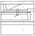
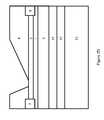
- FIG. 1shows a schematic of a cross-section of a half cell of an HFET.
- FIGS. 2( a ) to 2 ( m )depict schematic cross-sections of the device at various stages of processing.
- FIG. 3shows a schematic of the cross-section of an HFET in which the gate is accessed on the obverse face while the source and drain are accessed from the reverse face.
- FIG. 4shows a schematic of the cross-section of a grounded gate HFET with a stepped field plate.
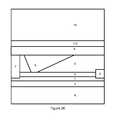
- FIG. 5shows a schematic of the cross-section of a lateral Schottky diode.
- FIGS. 6 and 7show schematics of the plan and cross-section views of an HFET in which sections of the original substrate are retained as an exoskeleton to maintain tensile strain in the active area of the device.
- FIGS. 8( a ) to ( f )show schematics of the cross-sections of an implementation with an exoskeleton at various stages of processing.
- III-nitride type devicesare techniques that enable III-nitride type devices to be formed using silicon base substrates.
- the obverse or device faceis the face of the wafer or epitaxial layer on which a lateral device is fabricated by forming electrodes that make ohmic and/or Schottky and/or metal-insulator-semiconductor (MIS) contacts to the semiconductor.
- the reverse faceis opposite to the obverse or device face.
- III-nitride materialor “III-N material” refers to a compound semiconductor material according to the stoichiometric formula Al x In y Ga z N, where x+y+z is equal to 1 or about 1.
- the devices described hereinare group III face devices.
- active layer(s)are a set of III-nitride layers in which devices are made, wherein changes of at least one potential barrier in the active layer due to voltages applied at terminals cause currents to flow through at least a pair of terminals in a desired fashion; and “active regions” are areal regions comprising of one or more cells of a semiconductor device.
- a cell of a power transistorfor example, as referred to herein includes a source, gate and drain, and the cell of a diode includes an anode and a cathode and the access region in between.
- devices described hereinare n-channel devices, but the general concepts can apply to p-channel devices as well.
- Some power devices formed with III-nitride layers on a silicon substrateutilize nucleation and stress management layers to enable proper formation of the III-nitride layers. Removal of the nucleation and stress management layers, which have high defect concentrations, is desirable to enable high voltage power devices to meet acceptable switching performance.
- To remove the defected layersone needs to access them by removing the mother substrate and then removing the defected epitaxial layers on the reverse face of the group-III nitride layers. To do this, the obverse face is mounted on an appropriate carrier wafer. The substrate on which the growth was initially made, i.e., the mother substrate, is removed and then the defected layers are removed.
- a suitable passivation layeris applied.
- the passivation layerensures high voltage operation without the negative impact of trapping.
- a thin active layerby itself is not capable of supporting high voltage operation and without the passivation layers on both faces, the exposed surface of the thin active layer is susceptible to trapping effects and the high surface fields may also cause dielectric breakdown of air.
- Appropriately patterned metallizationscreate the necessary contacts for the device.
- two or more contacts or other itemsare said to be “electrically connected” if they are connected by a material which is sufficiently conducting to ensure that the electric potential at each of the contacts or other items is about the same at all times.
- Lift-off of a III-nitride epitaxial film and removal of the nucleation layercan modify the strain in the film and affect the polarization charge.
- Management of strain and thence polarization chargeare important considerations in the design of high voltage lateral devices.
- Another considerationis that removal of the mother substrate and the buffer layer can affect the strain in the active layer. Strain in the active layer might be modified when the mother substrate and/or the nucleation and stress management layers are removed. Strain in the active layer might also be modified during the process of depositing thick passivation layers or bonding or attaching the active layer to a handling or carrier substrate. Modification of strain in the active layer can mean modification of the polarization charge, which affects the electrical parameters of the device.
- the amount of lattice strain in the active layer during growthis so high that strain relief happens by formation of dislocations and stacking faults or other defects that relax the lattice strain and stabilize the strain in the layer.
- the strain management layercan effectively contain the lattice mismatch between the substrate and the epi layer at the growth temperature or if the grown epi layer is thin, there is little strain. Therefore strain relief in the upper layers by the formation of defects does not occur during growth. However, as the wafer is cooled down to room temperature, strain develops in the III-nitride epi-layers if there is mismatch of thermal coefficients of expansion of adjacent layers.
- the strain caused in the III-N layers by the mismatch of thermal coefficients of expansionis tensile if the substrate is silicon.
- the polarization chargeis adequate to form a 2DEG required for low on-resistance devices.
- crystal straindoes not change much when the epitaxial layer is lifted off from the substrate.
- high quality strained films with low defect densityrelax substantially to relieve strain after substrate removal and polarization charge and thence the 2DEG can get substantially reduced.
- featurescan be incorporated in the device structure to prevent tensile strain and thence 2DEG collapse or a suitable amount of modulation doping can be added in the AlGaN barrier layer to maintain the desired 2DEG charge density.
- a suitable amount of modulation dopingcan be added in the AlGaN barrier layer to maintain the desired 2DEG charge density.
- no structure modification or process that creates stressesshould affect the strain in the active layer deleteriously.
- a full cellis formed by juxtaposing a laterally inverted half-cell next to the half cell.
- a power devicecan include many full cells in parallel, the cells being connected by on-chip busses to bonding pads.
- access to source or drain contactsis shown through vias located in the half cell itself. While connecting the source and drain contacts through vias in the half cell is possible for many situations, in some cases it can be a better to have vias, especially vias through the III-nitride layers, at nearby busses or at via pads located away from the active regions of the device. This would be an engineering decision based on many factors such as device layout, current density, device size, etc, and this application includes those cases in which contacts are accessed at locations away from the active device.
- a HFETis formed with gate and source contacts on an obverse face and a drain contact on the reverse face, as shown in FIG. 1 .
- Layers 1 , 2 , and 3are III-nitride semiconductors.
- Channel layer 1is an unintentionally doped or p ⁇ doped III-nitride layer in which the channel of the device is formed and a 2DEG sheet may lie.
- Barrier layer 2has a bandgap larger than that of the channel layer 1 .
- Spacer layer 3has a bandgap not smaller than that of the channel layer 1 and can be a multilayer structure.
- the spacer layer 3separates the channel layer 1 from the reverse face passivation layer.
- layers 1 to 3are high quality layers, carrier trapping or scattering in these layers, which affects device current, is reduced. Defects in these layers also affect leakage current and breakdown voltage.
- a stack of III-nitride semiconductor material layers 100can include a channel layer 1 , a spacer layer 3 and a barrier layer 2 , with the channel layer 1 between the spacer layer 3 and the barrier layer 2 .
- the channel layer 1 , barrier layer 2 and spacer layer 3are each formed of III-N materials.
- the bandgap of the barrier 2is greater than the bandgap of the channel layer 1 , which enables a 2DEG to form in the channel layer 1 near the interface of layers 1 and 2 .
- a cap layer(not shown) is on an opposite side of the barrier layer 2 from the channel layer 1 and has a smaller bandgap than the barrier layer 2 and can either be unintentionally doped or p-doped.
- the bandgap of the spacer layer 3is at least as great as the bandgap of channel layer 1 .
- the spacer layer 3is formed of multiple layers of material that have different composition from one another.
- dielectric materialsuch as silicon nitride, aluminum nitride, silicon oxide, alumina or various combinations of any of these or other suitable dielectrics, which may be a combination of inorganic or organic dielectrics, for example, polyimide, benzocyclobutene (BCB) or SU8 or a combination of two or more of these, is on the opposite side of the spacer layer 3 from the channel layer 1 .
- a device side passivation layer 5 of dielectric materialssuch as inorganic dielectrics, for example, silicon nitride, aluminum nitride, alumina or silicon oxide, or organic dielectrics, for example, polyimide, benzocyclobutene (BCB) or SU8 or a combination of two or more of these, can be on the opposite side of the stack of III-nitride semiconductor material layers 100 from the reverse side passivation layer 4 .
- the passivation layerscan be formed from dielectrics that have a large conduction band offset with respect to III-nitrides, create fewer surface states on the III-nitride cap layers and have low trap density so that there is no trap assisted tunneling or hot carrier trapping in the dielectric.
- Gate 6with an integral sloping field plate, is formed from an electrically conducting layer such as metal or a degenerately doped semiconductor covered with a metal that forms an ohmic contact with the degenerately doped semiconductor.
- an electrically conducting layersuch as metal or a degenerately doped semiconductor covered with a metal that forms an ohmic contact with the degenerately doped semiconductor.
- an appropriate dielectric(not shown) might lie between the gate 6 and the barrier layer 2 .
- Source 7can be formed from a metal or a highly doped n-type semiconductor and a metal layer that makes an ohmic contact to the highly doped n-type semiconductor.
- the source 7injects electrons to the channel layer 1 .
- Drain 8is a metal or a highly doped n-type semiconductor and a metal layer making an ohmic contact to the highly doped n-type semiconductor.
- a metal plug 15connects the drain 8 to reverse side drain contact 16 that is adjacent to the reverse side passivation layer 4 .
- the reverse side drain contact 16enables the drain 8 to be connected to the reverse side of the device.
- a passivating insulator 14 on the sidewall of a via that is subsequently filled with conductive material, here the via leading to the drain 8passivates and insulates the stack of III-nitride semiconductor material layers 100 from the metal plug 15 , that is, the plug that is formed by filling the via.
- a thermally and electrically conductive layer 17is on a side of the reverse side drain contact 16 opposite to the reverse side passivation layer 4 . The thermally and electrically conductive layer 17 is between the reverse side drain contact 16 and a thermally and electrically conducting substrate 18 .
- FIGS. 2( a - m )Various stages of one implementation of processing for a HFET (the half cell cross-section of which is shown in FIG. 1 ) are shown schematically in FIGS. 2( a - m ).
- a substrate 13such as a substrate formed of ⁇ 111> silicon or other suitable material, such as c-plane sapphire or SiC cation-face III-nitride layers are grown by an appropriate heteroepitaxial process.
- the substrate 13is sometimes referred to herein as the mother wafer or mother substrate.
- the substrate 13is eventually removed, leaving the stack of III-nitride semiconductor material layers 100 with little strain relaxation.
- the cation-face III-nitride layersinclude, in the following order from the substrate 13 , a nucleation layer 12 , which can be AlN/Al x Ga 1-x N, a stress management stack 11 , which can be a AlN/GaN or a Al x Ga 1-x N/GaN superlattice, the spacer layer 3 , which can be GaN or Al x Ga 1-x N with x less than 0.1, the channel layer 1 , which can be GaN, and the barrier layer 2 , which can be Al x Ga 1-x N with x more than 0.15.
- a nucleation layer 12which can be AlN/Al x Ga 1-x N
- a stress management stack 11which can be a AlN/GaN or a Al x Ga 1-x N/GaN superlattice
- the spacer layer 3which can be GaN or Al x Ga 1-x N with x less than 0.1
- the channel layer 1which can be GaN
- a source 7 and drain 8are formed from ohmic contacts that are deposited on the stack of III-nitride semiconductor material layers 100 and annealed.
- the exposed obverse surface of barrier layer 2is passivated by depositing an insulator material, such as silicon nitride, aluminum nitride, silicon oxide a polymeric dielectric or some combination thereof to form the device side passivation layer 5 .
- the device side passivation layer 5can be deposited using a suitable dielectric deposition scheme, such as CVD, PECVD, atomic layer deposition (ALD), sputtering, or spin on, as shown in FIG. 2 c.
- a gate trenchis formed with field-reducing sloped sidewalls by recess-etching the device side passivation layer 5 , as shown in FIG. 2 d.
- a viais made that extends to the source 7 .
- the via and gate trenchare filled with metal. Filling the gate trench forms the gate 6 and filling the via extends the source 7 . Subsequently, the exposed surfaces of the gate 6 and the source 7 are passivated with a protective layer 9 that can be selectively removed for bonding wires to the source and gate bond pads. Forming the passivation layer 9 completes the fabrication steps on the obverse of the structure 111 .
- the obverse face of the structure 111is attached to a handling wafer 10 .
- the handling wafer 10can be adhered to the structure 111 using an adhesive 112 that is easily removable, such as a polymer adhesive system that loses its adhesive quality when exposed to solvent, heat or radiation, such as UV light.
- the obverse faceis attached to battery powered mobile electrostatic wafer chuck.
- the mother substrate 13 on which the III-nitride layer was grownis removed.
- the substrate 13is thinned down to below 100 micrometers by lapping or a fast coarse etch.
- the remaining portion of the substrate 13 after thinningcan be removed by wet etching or fluoride-based plasma etching followed by wet etching to the III-nitride nucleation layer 12 .
- the III-nitride layercan be lifted-off using near UV laser radiation or, if an appropriate interfacial layer is between the substrate 13 and nucleation layer 12 , which can be removed by chemical liftoff.
- the process used to achieve lift-offis selected to create little change of strain over the active area of the device.
- the nucleation layer 12is removed, such as by etching in a chlorine-based plasma or by wet etching, if need be using electrochemical wet etching. Removing the nucleation layer 12 is followed by etching away the stress management layer 11 , as shown in FIG. 2 j , such as by using a process that does not introduce point defects in the spacer layer 3 .
- a reverse side passivation layer 4is deposited on the exposed reverse face of the spacer layer 3 , as shown in FIG. 2 k .
- the reverse side passivation layer 4can be a rather thick layer so that the layer can withstand the maximum drain-source voltage the device is expected to withstand.
- the reverse passivation layershould be at least 5 microns thick low leakage dielectric comprised of one or more inorganic or organic dielectric mentioned earlier such that the reverse side passivation layer 4 is a good electrical insulator for III-nitride semiconductors.
- the reverse side passivation layerhas interface state density of less than 10 12 /cm 2 , such as less than 10 10 /cm 2 and a bulk trap density less than 10 20 /cm 3 , such as less than 10 18 /cm 3 .
- the bulk trap densitycan indicate traps in the passivation layer that make a device more leaky or give their characteristics hysteresis.
- a viais formed through the reverse side passivation layer 4 , the spacer layer 3 , and the channel layer 1 to reach the drain 8 .
- the via side wallsare passivated by forming a passivating insulator 14 and the via is filled with a conducting metal plug 15 that makes good electrical contact to the drain contact metallization 8 on the obverse face of the device. While the via is shown to be in the active region of the device (and it might have to be located there for an enclosed drain cell configuration), it need not be so.
- the viacould be located at a via/contact pad away from the active regions of the device, because that may reduce reverse leakage and increase breakdown voltage.
- a reverse side drain contact 16is able to interconnect multiple drain vias when multiple half cells are formed (not shown in this figure).
- the reverse side drain contact 16is used for attaching the wafer to a thermally and electrically conducting layer 17 .
- the thermally and electrically conducting layer 17can be an adhesive layer that thermally and electrically contacts a conducting substrate 18 .
- the handling wafer 10is then removed and subsequently the temporary layer 9 is selectively removed to expose the source 7 and gate 6 .
- the source 7 and gate 6can then be attached to bonded leads (not shown).
- the waferis then tested and scribed for downstream processing, such as die-attach and bond.
- the gate with a sloping field plateis grounded.
- the source 7 and drain 8are both covered by the device-side passivation layer 5 .
- the gate with integrated sloping field plate 6extends over the device-side passivation layer 5 , so that the device-side passivation layer 5 is between the source 7 and the gate 6 in a lateral direction and the device-side passivation layer 5 is between the drain 8 and the gate 6 in a lateral direction.
- the lateral directionis a direction perpendicular to the direction in which the main surface of the layers of the stack of III-nitride semiconductor material layers 100 extends.
- the passivating insulator 14is on the sidewall of vias that lead to the drain 8 and source 7 contacts on the obverse face of the stack of III-nitride semiconductor material layers 100 .
- the passivating insulators 14passivate and insulate the part of the active layer, that is, the stack of III-nitride semiconductor material layers 100 , from the metal plugs 15 and 25 that respectively connect the drain contact 8 and the source contact 7 to the drain interconnect metallization 16 and the source interconnect metallization 26 on the reverse face.
- the reverse faceis covered with a passivating dielectric layer 20 in which contact holes are open at bonding pads for the source and the drain.
- Carrier wafer 19is an electrically and thermally conducting wafer to which the obverse face of the device 120 is bonded.
- a bonding layer 29which is also an electrical and thermal conductor, bonds carrier layer 19 to the gate 6 of the device 120 .
- the sourceis to be accessed from the reverse face, vias to the source 7 are not required on the obverse face and there is no need to cover the gate metallization with a protective coat (such as layer 9 in FIG. 2 e ) as in the previous process.
- a protective coatsuch as layer 9 in FIG. 2 e
- the waferis permanently attached to the conducting carrier wafer 19 .
- the vias to the drain and source contactscan be made in the same process steps.
- an HFETis formed with a stepped field plate connected to the grounded gate. Additional metal layers 21 and 22 are in contact with the gate 6 and with the bonding layer 29 .
- the gate 6along with the additional metal layers 21 and 22 form a stepped field plate 96 .
- the stepped field plate 96can be formed by a series of lithography steps, including partial etch of dielectric material and metal deposition.
- the stepped field plate 96includes part of the gate layer 6 that overlays the gate dielectric 5 , and metal layers 21 and 22 .
- the stepped field plate 96is formed of layers that are deposited in the recess of the device side passivation layer 75 , which is deposited over the gate dielectric 5 and the gate 6 .
- the passivation layer 75can be deposited in a series of steps. A recess is formed in the passivation layer at each step of the deposition.
- the first field plate layer 21is formed in a recess in one of the first sublayers of the passivation layer 75 .
- the passivation layer 75is further patterned and another metallization to form the second field plate layer 22 is made so that the formed field plate over the device side passivation layer 75 is in contact with the lower field plate layer 21 . Because the three portions are in electrical connected with one another, they function as a single component.
- the stepped gate and field plate 96can be formed from more or fewer sections than the three that are shown, using other deposit-pattern-deposit processes that form the metal or other conducting material structure in the dielectric layer.
- the wafer 121 with the device fabrication complete on the obverse faceis attached to a conducting carrier wafer 19 with a conducting layer 29 and the reverse face processed as for the device in FIG. 3 .
- a lateral Schottky diodecan be formed using the techniques described herein.
- a Schottky diodeis formed by an appropriately chosen metal making contact with a semiconductor which is called the Schottky layer.
- the Schottky diode materials and structureare engineered to obtain acceptable forward voltage (such as ⁇ 0.5 V at 1 mA/mm) and forward on resistance (R on ⁇ 10 ⁇ /mm for a 1000 V device).
- AlGaN stackforms the active layer with an ohmic contact to the 2DEG forming the cathode and the metal of the Schottky contact forming the anode.
- the top AlGaN layeris etched so that the anode metal layer makes direct contact to the Schottky layer as shown in FIG. 5 .
- the stack of III-nitride semiconductor material forming the active layer 200can include a Schottky layer that also serves as the barrier access layer which we shall call the Schottky-cum-access layer 201 , a spacer layer 203 and a polarization induced dipole (PID) layer 202 , with the Schottky-cum-access layer 201 between the spacer layer 203 and the PID layer 202 .
- the active stackis designed so that a 2 DEG forms in the Schottky-cum-access layer when the complete sandwich is intact.
- there is a cap layer on top of PID layer 202that has a smaller bandgap than the PID layer 202 and is unintentionally or p ⁇ doped.
- the spacer layer 203has a bandgap not smaller than the bandgap of the Schottky-cum-access layer 201 and can be a single or multilayer structure.
- the Schottky-cum-access layer 201is an unintentional or n doped III-nitride layer which forms the Schottky layer of the diode where the anode metal 206 makes contact and the lateral access layer elsewhere, with the 2-DEG forming a low resistance access path to the cathode contact 8 .
- the doping of the Schottky-cum-access layeraffects the forward cut-in voltage of the diode. The higher the n-type doping, the lower the saturation current and the larger the forward cut-in voltage of the Schottky diode. However, as one raises the n-type doping the 2-DEG mobility drops and the access region resistivity increases.
- a passivating dielectric 205is deposited on the active layer.
- the dielectric layer 205 and the PID layer 202are etched where the anode metal 206 must make a Schottky contact with the Schottky layer 201 . Because the PID layer is removed, there is no polarization induced dipole and therefore 2-DEG below the anode metal 206 and a good Schottky barrier is formed. The PID layer and 2-DEG however remain in the access regions.
- Anode 206is formed of a metal with a work function that provides the requisite turn-on voltage.
- an integral sloping field plateis formed with the anode by the formation of a sloped recess in the passivation layer 205 before the deposition of the anode metal 206 and then a conducting metal 207 on it to reduce the on-resistance of the diode.
- the cathode contactis an ohmic contact 208 which is an electron collecting layer forming good electrical contact to the 2DEG in the access region.
- Contact 208is a metal alloy or a highly doped n-type semiconductor with a layer of metal making an ohmic contact to the highly doped n-type semiconductor.
- the reverse faceis processed using processes similar to those for the HFETs described earlier, such that the mother wafer and the defected layers are removed, a first reverse passivation layer 4 is deposited, vias are etched in it and the cathode contact brought to the reverse face using metal plug 15 and metallization 16 .
- a second reverse face passivation layer 20protects the reverse face and is opened only where contacts are required for one or more bonding pads for the cathode on the reverse face (not shown).
- the diodeincludes an implanted guard ring in the barrier layer to reduce leakage currents.
- a stiff adhesive layeris used to anchor the device face to a carrier wafer.
- polymeric dielectrics with a Young's modulus less than one hundredth that of GaNare not used for the device side passivation layer 5 , because of the strain relief that can occur due to the plasticity of the dielectric.
- Even amorphous silicon dioxide with its Young's modulus one fifth that of GaNmay be inadequate to prevent an adjacent GaN active layer, the channel layer 1 and the barrier layer 2 , from strain relaxation.
- the stiffness of silicon nitridemay be adequate to maintain strain in the active layer if it is rigidly bonded to it. However, hydrogen and nitrogen broken bonds in the silicon nitride layer can lead to trapping effects which may be undesirable in a high voltage device.
- strain in the III-nitride active layersis maintained by using sufficiently hard and thick passivation layers, such that strain is maintained in the III-nitride layers and one can then attach the device to a carrier wafer that can handle the heat dissipation and if need be the electrical contact.
- Engineering the electrical, mechanical and thermal properties of the obverse and reverse face passivation layersis a challenge and again not addressed here.
- some of the substrate on which the device is formedis retained so that a III-nitride membrane is maintained with the tensile strain created during hetero-epitaxy and cool down.
- a planar exoskeletonis used to lock in-plane tensile strain in all layers of the active layer.
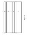
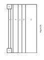
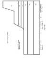
- An exemplary plan view of such a dieis shown in FIG. 6 .
- the die 30includes cell regions 31 each including multiple cells that form the power device or other high voltage drive circuits. Each region 31 may have from a few to tens of cells with the reverse face processed such that the defected layers that have traps have been removed. Bonding pads 32 , 33 for the gate and the source are at either end of the die 30 .
- the die 30can include more than one bonding pad for each terminal to satisfy impedance matching and current handling requirements of the power device plus control and feedback inputs and outputs if on-chip control is present.
- On-chip control and drive circuitsthat handle low voltage (such as, ⁇ 30 V) which could be in the active GaN layer 34 or in the silicon below 35 (both indicated areally) are optionally placed on the die 30 .
- Areas 36 surrounding the cell regions 31 , the bonding pads 32 , 33 and on-chip control and drive circuits 34 , including areas below the optional silicon control electronics regions 35indicate the areal location of the strain maintaining exoskeleton, formed by keeping portions of the substrate on which the device is formed intact.
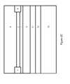
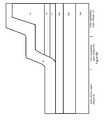
- FIG. 7the cross-section along plane X 1 X 2 X 3 in FIG. 6 is shown.
- Cross-sections above A, B and Crespectively depict the cross-sections in the active device region (around X 1 ) or the high voltage device region, the inner exoskeleton region (around X 2 ) and the outer exoskeleton region (around X 3 in the bond pad region).
- the metallization on the reverse face that connects the drain viasis extended to the bond/solder pads on the inner exoskeleton.
- Region Bis the inner exoskeleton that is next to the device region (around X 2 ) and can maintain the tensile strain in the III-nitride film in the active region.
- a layer of silicon ( 43 ) from the mother waferis between about 10 and 50 microns thick. This thickness enables the tensile strain to be maintained and at the same time enables the drain metallization from the active region 16 to extend over to the inner exoskeleton (Region B) through metallization 49 .
- a thicker inner exoskeletonwould require an unnecessarily large area for the sloped portion that enables reproducible and reliable interconnect coverage on the sidewall of the exoskeleton.
- Thick dielectric layers 44 , 45insulate the silicon 43 from the drain metallization 49 .
- nucleation and stress management layers 42are not removed in the exoskeleton regions B and C, which helps to keep the active III-nitride layer 41 firmly attached to the exoskeleton.
- the active III-nitride layer 41can include channel layer 1 , barrier layer 2 and spacer layer 3 and can be isolated electrically by oxygen implantation along the perimeter of the active region.
- Layer 46comprises the passivation 5-metallization 6/7-passivation 9 stack of layers, which carry source or gate connections to bonding pads in Region C.
- an additional areal stress management layercan be added between the perimeter of the active region and the inner perimeter of the exoskeleton.
- Region Cis the outer exoskeleton and it lies along the perimeter of the die 30 , below bond pads on the obverse face and other regions that have low voltage electronics. As shown in FIG. 7 the outer exoskeleton retains thicker silicon from the mother wafer—the thickness being adequate to enable handling of the wafer during processing, dicing and packaging subsequent to the thinning operation while preventing damage to the assembly. For smaller wafers (such as 2′′ wafers) and small area dies (less than 3 ⁇ 3 mm 2 ), the thickness of the silicon in Regions B & C can be kept the same to reduce processing steps. As can be seen in FIG.
- layer 47represents the obverse face passivation 5-metallizations 6/7-passivation 9 layers with the top passivation removed near the bond pad, where an additional metal layer ( 48 ) might be added, the latter necessary for some bonding and packaging situations. Additionally, a layer of silver might be added as layer 49 if soldered contacts are needed, whereas, ultrasonic bonding could be done directly to a pad on a gold bus.
- the metallizations (6/7)are thickened at the main bus level and there may be more than one bond/solder pad for one terminal.
- the thicker exoskeletoncan also support any low voltage control and synchronization electronics on the silicon mother wafer, such as in non-active regions of the power device.
- the process flowcan be similar in the early phase to the processes we have presented earlier.
- a basic high voltage device with gate and source contacts on the obverse or device faceis fabricated and attached to a handling wafer with thermal or UV release polymer, as described herein.
- the mother substrateis thinned down on the reverse face to a desired thickness.
- a photoresist or oxideis selectively applied to the reverse face in Region C, such as by using a coarse double sided alignment, the exposed pockets of Regions A and B are etched, such as by a deep RIE process to the requisite depths.
- a second photolithography stepis performed to protect Regions B & C, and the silicon plus the nucleation and stress management layers from the Region A are removed. These layers can be removed by deep RIE and a sloping sidewall with a slope between about 30° to 75° can be formed in the silicon exoskeleton since steeper sidewalls could create discontinuities in metallization from the active region to the inner exoskeleton as explained earlier. Completion of etch through a layer can be conveniently determined by end point detectors based on measuring the intensity of silicon or gallium emissions. The etch process is terminated by either a wet etch or a nitrogen plasma low temperature anneal to reduce defect generation in the active layers.
- a thick layere.g., a layer about 15 ⁇ m thick on 1000 V device, of passivating strain-free insulator, such as silicon dioxide or silicon oxynitride, is deposited using a chemical vapor deposition technique such as ICP-CVD.
- the handling waferis detached and the deposited dielectric is densified by either a thermal or excimer laser anneal to improve passivation at high fields and reduce long term moisture diffusion—thence device drift—into the passivation layer.
- the handling wafercan be reused.
- a via to the drain contactis made on the reverse face to the drain metallization on the obverse face, the sidewalls passivated, and the via is filled with metal such as copper or gold.
- a patterned metallization that connects the drain via to the bond/solder pads on the inner exoskeletonis formed. If required an additional bond/solder pad metallization is performed and only the bond pads exposed through a final passivation layer. Devices are tested and diced for downstream processes.
- the metallizationoccurs late in the process of forming the device, but can enable a much higher quality passivation, produce devices with higher breakdown voltage and lower trapping (thence lesser current collapse and hysteresis in characteristics), utilize fewer process steps, does not require an expensive double sided aligner and can enable better integration of silicon and III-nitride processes.
- the active layer 100is grown by heteroepitaxy on a support stack of a ⁇ 111> silicon mother wafer 13 , a nucleation layer 12 and a stress management layer 11 .
- the active layer 100comprises three essential layers, with acceptably low defect density, that are the spacer layer, the channel layer and the obverse barrier layer, plus other optional layers that might include a reverse barrier layer, a cap layer and a alloy scattering screening layer.
- a passivation stack 105is a sandwich of one or more inorganic dielectrics such as aluminum nitride, silicon nitride and silicon dioxide.
- the passivation stack 105can be deposited by a low to moderate temperature CVD process.
- FIG. 8 cwhich shows the cross section spanning the active region, the inner exoskeleton and the outer exoskeleton after the reverse face is processed.
- the obverse face of the waferis attached by a UV sensitive adhesive layer (not shown) to a double sided polished quartz wafer 150 .
- a photoresist patternis used to protect a region of the mother wafer 13 that will form the outer exoskeleton and expose regions that will form the inner exoskeleton.
- the exposed siliconis etched, such as with a deep reactive ion etch process, for example, the Bosch process until the desired thickness of the inner exoskeleton is reached.
- a second lithography stepis performed to pattern the active areas and the remaining silicon and nucleation and stress management III-nitride layers are removed by dry and wet etching, leaving only the active layer intact.
- a conformal coating of a sandwich of inorganic dielectric materialis deposited to form passivation layer 51 , such as by a low temperature remote plasma CVD process on the micromachined reverse face.
- the quartz handling waferis then detached. If the adhesive was a UV decomposable polymeric adhesive, UV light is shone on the adhesive through the quartz wafer 150 , causing the adhesive to lose its adhesive quality. This is followed by a medium temperature anneal to densify the passivation layers and reduce dielectric traps and fixed oxide charges.
- the passivation layer 51is patterned for implantation of an n′-drain 52 , the field shaping region and contact to the 2DEG layer which is closer to the obverse side.
- a high temperature annealis used for implant activation and to reduce traps in inorganic dielectrics.
- the high temperature annealproduces a far higher quality dielectric than is possible by lower temperature anneals.
- High temperature annealingthat is annealing at temperatures over 750° C. may not be possible after metallization, because the high temperatures can cause the metallization to melt or alloy, and so cannot be done with the early metallization processes described previously.
- the reverse faceis patterned and metalized to form the drain ohmic contact 53 , as shown in FIG. 8 e .
- the obverse faceis patterned and metalized to form the source ohmic contact 54 .
- the waferis optionally annealed at a high temperature for a short time after metallization to form good ohmic contacts to both the source and drain in the active layer 100 next to metallizations 54 and 53 .
- the obverse faceis further patterned for the Schottky gate metallization 55 , if need be, by depositing it over a thin gate dielectric.
- the Schottky gate metallization 55 formationcan be followed by a mid temperature anneal (400-600° C.) to improve the Schottky barrier interface.
- the waferis patterned on both faces and the metallization to form busses and bond/solder pads is thickened by electro or electroless deposition. Both faces of the wafer are passivated, such as by using a low temperature CVD deposition of silicon nitride or depositing some other capping passivation dielectric. Contact holes are opened to the bond/solder pads.
- the waferis diced for downstream package and test processes.
- a modification of the process for medium voltage power devicescan include forming the gate, source and drain access on the obverse face.
- the n+-drain implant and the drain metallizationare both on the obverse face.
- metal alloys for the ohmic contacts and the gate metalrequire similar post-metallization anneal conditions and that enables further simplification of the process sequence.
- control, synchronization and drive electronicscan include fabrication of control, synchronization and drive electronics on the silicon exoskeleton if silicon devices are required.
- control, synchronization and drive electronicscould be hybrid silicon-GaN or only GaN with the low voltage GaN devices located in the active regions or the exoskeleton regions.
- Yet another modification of the deviceforms the source and drain access on the reverse face.
- a lateral Schottky diode with the barrier accessed by one or more 2DEG layerscan be formed using the methods described herein.
- the anodecan be accessed on the obverse face and the cathode the reverse face.
- Nucleation and stress management layersare grown by heteroepitaxy followed by a p-type/unintentionally doped GaN layer, an unintentionally doped AlGaN layer, an unintentionally or lightly doped GaN layer and an in situ silicon nitride layer.
- the device areais delineated by implant or mesa isolation. Additional dielectric layers can be deposited. The dielectric layers are removed after patterning and the metal forming the ohmic contact with the 2DEG is deposited and annealed.
- the obverse faceis then patterned for the Schottky contact and the dielectric layers are removed by etching.
- another lithography stepis performed to define a guard ring, after which the metal to form the Schottky barrier is deposited and annealed.
- a thick dielectricis deposited and patterned to expose areas where the metal needs to be thickened.
- the anode electrode busis further thickened by electroless plating of nickel or gold.
- the waferis planarized until the top of the thickened metal and a metal coating is exposed. This face is then attached to an electrically and thermally conducting wafer using a conducting interlayer.
- the wafer on the obverse faceis protected by an appropriate coating and the original substrate is removed by etching.
- the nucleation and stress management layersare etched and the reverse surface is treated with an appropriate wet etch or nitrogen plasma to remove residual surface damage and charge.
- the reverse faceis next suitably passivated with silicon nitride or aluminum nitride and if need be an additional layer of silicon dioxide.
- Other organic, such as BCB, or inorganic, such as alumina, dielectricscan alternatively or also be used.
- One or more vias through the passivation layer and the underlying group III-nitride layersare etched to the cathode bus. Terminal metallization is performed with a two step deposit and plate process. The wafer is then sawed to form separate dies for downstream processing.
- the process of formationcan be as follows. Nucleation and stress management layers are grown by heteroepitaxy followed by a p-type/unintentionally doped GaN layer, an unintentionally doped AlGaN layer, an unintentionally or lightly doped GaN layer and finally an in situ silicon nitride layer. Additional dielectric layers can be deposited. After implant isolation, dielectric layers are removed. After patterning and the metal forming the ohmic source and drain contacts with the 2DEG is deposited and annealed.
- the obverse faceis then patterned for the Schottky gate contact between the source and drain and the dielectric layers are removed by etching. This can be followed by another lithography step to define a field plate, after which the metal to form the gate contact is deposited and annealed. Dielectric deposition and patterning is then performed to form the gate interconnect and bus.
- the gate and source electrode bussesare further thickened by electroless plating of nickel or gold or copper. Next a thick dielectric is deposited and the wafer is planarized until the top of the thickened metal is exposed.
- the waferis then attached to a handling wafer.
- the wafer on the obverse faceis protected by an appropriate coating and the original substrate is removed by etching.
- the nucleation and stress management layersare etched and the reverse surface is treated with an appropriate wet etch or nitrogen plasma to remove residual surface damage and charge.
- the reverse faceis next suitably passivated with silicon nitride or aluminum nitride and if need be an additional layer of silicon dioxide.
- Other organic, such as BCB, or inorganic, such as alumina, dielectricscan also be used.
- One or more vias through the passivation layer and the underlying group III nitride layersare etched to the drain bus and via filled with metal plug.
- the reverse faceis then bonded to an electrically and thermally conducting substrate so that the drain vias are in electrical contact with the wafer and the dielectrics in mechanical contact.
- the handling waferis then removed to expose the source and gate metallization busses.
- the topis then coated with a organic or inorganic passivation layer that is open at only the source and gate bonding pads.
- the waferis then sawed to form separate dies for downstream processing.
- An etch stop layersuch as a layer of AlGaN
- An etch stop layercan be inserted into the spacer layer 3 to facilitate backside selective dry etching using fluoride- and chloride-based chemistry mixtures. This can provide better control of the remaining thickness of the spacer layer after the backside processing.
- Another possible modificationis to introduce an insulating dielectric layer under the gate 6 to suppress gate leakage current.
- Possible gate dielectricincludes but are not limited to silicon nitride, silicon oxide, aluminum nitride, aluminum oxide, gallium oxide and high K dielectrics.
- III-nitride semiconductor layerinstead of a dielectric layer to form device side passivation layer 5 .
- a field-reducing platecan be applied on the reverse side passivation layer 4 for the grounded gate.
- the field platecan be connected either to the source or to the gate.
- This field plate layeroverlaps gate 6 on the obverse face.
- a certain lateral distancecan be kept between the field plate layer and the drain 8 on the obverse face so that there is no shorting at high voltages.
- the III-nitride layerscan be grown as nitrogen faced layers, as described in U.S. application Ser. No. 12/209,504, filed on Sep. 12, 2008, and is incorporated herein by reference, instead of III-face layers.
- the III-nitride layerscan be grown with non-polar m-plane or a-plane, or semi-polar faces instead of c-plane faces.
- the channel layer 1can be modulation doped in structures in which there is no polarization charge due to strain collapse or due to use of a non-polar face orientation of the III-nitride active layer.
- FETssuch as HFET, MISFET or JFET devices
- gate and source contactsaccessed on the device face and the drain contact accessed on the reverse face
- Schottky diodeswith the cathode accessed via the reverse face and the anode accessed via the device face.
- Other combinations of gate, source, drain or anode and cathode locationsare possible as well.
- the gate, source and draincan all be on either the obverse or the reverse face.
- the drain and gatecan be on one side, such as the reverse side, while the source can be on the opposite side, such as the obverse side, or vice versa.
- the cathodecan be on the obverse face and the anode on the reverse face.
Landscapes
- Engineering & Computer Science (AREA)
- Physics & Mathematics (AREA)
- Condensed Matter Physics & Semiconductors (AREA)
- General Physics & Mathematics (AREA)
- Manufacturing & Machinery (AREA)
- Computer Hardware Design (AREA)
- Microelectronics & Electronic Packaging (AREA)
- Power Engineering (AREA)
- Junction Field-Effect Transistors (AREA)
- Formation Of Insulating Films (AREA)
- Insulating Bodies (AREA)
- Electrodes Of Semiconductors (AREA)
Abstract
Description
- This invention relates to semiconductor devices fabricated on group III-nitride semiconductors.
- Group III-nitride based devices have many potential material advantages over silicon based devices for high power electronics applications. Amongst others, these include larger bandgap and breakdown field, high electron mobility in a two dimensional electron gas (2DEG), low thermal generation current, and the possibility of using the direct bandgap plus a great variety of band and polarization engineering techniques applicable in many of these structures for novel device functions. However, applications have been hampered by a lack of low cost substrates for device fabrication.
- Devices are sometimes made by heteroepitaxy on suitable substrates such as silicon carbide, sapphire or silicon. Techniques for applying the layers can include molecular beam epitaxy (MBE) or metal organic chemical vapor deposition (MOCVD) and hydride vapor phase epitaxy (HYPE). High voltage devices of gallium nitride (GaN) can require thick GaN layers, such as 2-6 micron thick layers. It can be difficult to grow thick gallium nitride by heteroepitaxy. Various stress management techniques such as graded layers or superlattices and various compensation techniques such as iron (Fe) or carbon (C) doping are used to enable growth of thick layers and to enable high resistivity buffer layers.
- While the total thickness of the GaN buffer layer can be important in some devices, it can also be important to achieve a sufficiently thick layer of material with low defect density. The concentrations of extended and point defects that give deep levels in the band gap as well as dopants have to be low. This can facilitate operation of the device at high voltage without the device being subject to trapping, leakage or early breakdown effects.
- To accommodate a large voltage across the source/gate and the drain in a transistor, such as a heterojunction field effect transistor (HFET), or across the anode and the cathode in a diode, the spacing required between the electrodes to sustain the voltage typically has to be large—for example, a 1 kV device may need an electrode spacing of 10 microns or larger. Thus, high voltage lateral devices require large areas and need to be made on low cost substrates. Silicon substrates are typically the most cost effective substrates for formation of III-N type devices. However, due to the large lattice and thermal mismatch between silicon and gallium nitride, nucleation and stress management layers may be required. These layers, such as superlattice layers of AlxGa1-xN can have a high density of dislocations and other deep trapping centers. While this approach can produce acceptable spacer, channel and barrier layers, a high quality thick buffer layer is difficult to achieve. Because the layers below the spacer layer can have a high concentration of defect levels in the bandgap, this can cause drain voltage induced current collapse and leakage at high drain biases and can also reduce breakdown voltage of the device.
- In one aspect, a group III-nitride device is described that includes a stack of III-nitride layers, a first passivation layer, a second passivation layer and one or more conductive contacts. The stack includes a channel layer, a barrier layer directly adjacent to the channel layer and a spacer layer directly adjacent to a side of the channel layer opposite to the barrier layer. The channel layer includes a 2DEG channel in the channel layer adjacent to the barrier layer. The first passivation layer directly contacts a surface of the spacer layer on a side opposite to the channel layer, wherein the first passivation layer is an electrical insulator and the stack of III-nitride layers and the first passivation layer form a structure with a reverse side proximate to the first passivation layer and an obverse side proximate to the barrier layer. The second passivation layer is on the obverse side of the structure. The contacts are electrically connected to the 2DEG channel.
- In another aspect a method for forming a device is described. A nucleation layer is formed on a mother substrate, wherein the nucleation layer includes AN. A stress management layer is formed on the nucleation layer that is on the mother substrate, wherein the stress management layer includes a III-nitride material. A stack of III-nitride layers is formed on the stress management layer, wherein forming the stack includes forming a channel layer with a 2DEG channel therein, the stacking having an obverse face opposite to the stress management layer. The obverse face of the stack is attached to a carrier wafer. An entirety of the mother substrate, the nucleation layer and the stress management layer is removed, wherein the removing step exposes a reverse surface of the stack. The reverse surface is passivated with a dielectric layer.
- In yet another aspect a method for forming a device is described. A nucleation layer is formed on a mother substrate, wherein the nucleation layer includes AN. A stress management layer is formed on the nucleation layer that is on the mother substrate, wherein the stress management layer includes a III-nitride material. A stack of III-nitride layers is formed on the stress management layer, wherein forming the stack includes forming a channel layer with a 2DEG channel therein. At least a portion of the mother substrate, a portion of the nucleation layer and a portion of the stress management layer is removed, wherein the removing step only removes a portion of the mother substrate and forms a thin exoskeleton portion and a thick exoskeleton portion, wherein the mother substrate is thinner in the thin exoskeleton portion than in the thick exoskeleton portion.
- Implementations of the devices and methods described herein may include one or more of the following features. The first passivation layer and the second passivation layer can each have a sufficiently large bandgap, sufficiently low bulk defect density and sufficiently low interface density so that breakdown of the device is improved in comparison with a device having the stack of III-nitride layers and lacking the first passivation layer and the second passivation layer. The first passivation layer can have an active interface state density of less than 1012/cm2 and an active bulk trap density less than 1020/cm3. The first passivation layer or the second passivation layer can be formed of an inorganic dielectric material. The first passivation layer or the second passivation layer can include silicon nitride, silicon dioxide, silicon oxynitride, alumina or aluminum nitride. The first passivation layer or the second passivation layer can be an organic dielectric material. The first passivation layer or the second passivation layer can include an organic resin. The organic resin can include one of polyimide, benzocyclobutene (BCB) or SU8. The passivation layer can include a stack of at least one organic dielectric material and at least one inorganic dielectric material. The conductive contact can be electrically connected to the reverse side of the structure. The stack of III-nitride layers can be between 0.5 and 30 microns thick. The device can include a gate contact and a gate dielectric, wherein the gate dielectric is between the stack of III-nitride layers and the second passivation layer. One of the one or more conductive contacts can be a gate contact on the obverse side of the structure; one of the conductive contacts can be a source contact on the obverse side of the structure; one of the conductive contacts can be a drain contact on the reverse side of the structure; and the second passivation layer can cover an entirety of the obverse side of the structure including a space between the gate contact and the source contact. The device can include a nucleation and stress management layer contacting the spacer layer; and a mother substrate that includes silicon, wherein the nucleation and stress management layer is between the stack of III-nitride layers and the mother substrate; wherein the device has a first portion including the stack of III-nitride layers and a second portion including the stack of III-nitride layers, the nucleation and stress management layer, and the mother substrate, the second portion forming an exoskeleton and the first portion can be free of the mother substrate and the nucleation and stress management layer. The device can include a dielectric layer on a side of the mother substrate that is opposite to the stack of III-nitride layers. The device can include a conductive layer, wherein the dielectric layer is between a metallization layer and the mother substrate. The exoskeleton can have a thin portion and a thick portion, wherein the mother substrate in the thin portion is thinner than the mother substrate in the thick portion and the conductive layer does not extend into the thick portion of the exoskeleton. The mother substrate in the thin portion can be between about 10 and 50 microns. A conductive layer can be on the obverse side that is connected to a conductive pad in the second portion. The exoskeleton can maintain sufficient strain in the stack of III-nitride layers to create a 2DEG in the channel layer. The second passivation layer can be confined to the first portion. At least one of a control, protection, synchronization or drive circuit on the exoskeleton can be in either the silicon or III-nitride active region. Forming the device can include forming conductive contacts that are in electrical contact with the 2DEG channel. The stack of III-nitride layers can include a barrier layer on a first side of the channel layer and a spacer layer on a second side of the channel layer; the spacer layer can include an etch stop layer; and the removing step can etch to the etch stop layer. The method can include forming an external contact to the 2DEG channel, wherein the external contacts extends through the dielectric layer. The method can include fabricating one of a diode or a transistor in the stack of III-nitride layers. The stack of III-nitride layers can include a barrier layer on a first side of the channel layer and a spacer layer on a second side of the channel layer; the spacer layer can include an etch stop layer and the removing step can etch to the etch stop layer.
- The object of forming a high voltage lateral group III nitride device may be achieved using one or more of the following techniques. An appropriate semiconductor stack can be fabricated by heteroepitaxy on a low cost substrate, which is subsequently removed after the obverse face of the epitaxial film is attached on a carrier wafer that also has appropriate metallization and vias. Substrate material can be thinned, which can include thinning of the epitaxial material. Defected nucleation and stress management layers that form the buffer layer can be removed. The reverse surface can be treated to remove near surface defects and covered with a passivation layer. Appropriate vias and metallization can make device terminals from the obverse face accessible on the reverse.
- Some of the devices described herein are fabricated using the layout and process best suited for a particular function in a hetero-epitaxial layer grown on a wafer/substrate, the wafer/substrate on which a device is formed is then mounted on another appropriate wafer and the initial wafer/substrate and the nucleation and stress management layers grown during hetero-epitaxy are removed; the reverse face is then passivated and contact vias opened for metallization to the upper electrodes. Depending on packaging requirements one chooses to have the final substrate on either the obverse or reverse face with the appropriate structures and processes to make contact with the device metallization pads.
FIG. 1 shows a schematic of a cross-section of a half cell of an HFET.FIGS. 2( a) to2(m) depict schematic cross-sections of the device at various stages of processing.FIG. 3 shows a schematic of the cross-section of an HFET in which the gate is accessed on the obverse face while the source and drain are accessed from the reverse face.FIG. 4 shows a schematic of the cross-section of a grounded gate HFET with a stepped field plate.FIG. 5 shows a schematic of the cross-section of a lateral Schottky diode.FIGS. 6 and 7 show schematics of the plan and cross-section views of an HFET in which sections of the original substrate are retained as an exoskeleton to maintain tensile strain in the active area of the device.FIGS. 8( a) to (f) show schematics of the cross-sections of an implementation with an exoskeleton at various stages of processing.- Like reference symbols in the various drawings indicate like elements.
- Described herein are techniques that enable III-nitride type devices to be formed using silicon base substrates.
- As used herein the obverse or device face is the face of the wafer or epitaxial layer on which a lateral device is fabricated by forming electrodes that make ohmic and/or Schottky and/or metal-insulator-semiconductor (MIS) contacts to the semiconductor. The reverse face is opposite to the obverse or device face. As used herein, the term “III-nitride material” or “III-N material” refers to a compound semiconductor material according to the stoichiometric formula AlxInyGazN, where x+y+z is equal to 1 or about 1. The devices described herein are group III face devices. However, the techniques described herein can be applied to N-face devices with the appropriate change in the relative location of the 2DEG layer and layer type (i.e., whether the layer is p- or n-type or intrinsic). As used herein, “active layer(s)” are a set of III-nitride layers in which devices are made, wherein changes of at least one potential barrier in the active layer due to voltages applied at terminals cause currents to flow through at least a pair of terminals in a desired fashion; and “active regions” are areal regions comprising of one or more cells of a semiconductor device. A cell of a power transistor, for example, as referred to herein includes a source, gate and drain, and the cell of a diode includes an anode and a cathode and the access region in between. Additionally, devices described herein are n-channel devices, but the general concepts can apply to p-channel devices as well.
- Some power devices formed with III-nitride layers on a silicon substrate utilize nucleation and stress management layers to enable proper formation of the III-nitride layers. Removal of the nucleation and stress management layers, which have high defect concentrations, is desirable to enable high voltage power devices to meet acceptable switching performance. To remove the defected layers one needs to access them by removing the mother substrate and then removing the defected epitaxial layers on the reverse face of the group-III nitride layers. To do this, the obverse face is mounted on an appropriate carrier wafer. The substrate on which the growth was initially made, i.e., the mother substrate, is removed and then the defected layers are removed. After removal of the mother substrate and one or more defected layers, a suitable passivation layer is applied. The passivation layer ensures high voltage operation without the negative impact of trapping. Also, a thin active layer by itself is not capable of supporting high voltage operation and without the passivation layers on both faces, the exposed surface of the thin active layer is susceptible to trapping effects and the high surface fields may also cause dielectric breakdown of air. Appropriately patterned metallizations create the necessary contacts for the device. As used herein, two or more contacts or other items are said to be “electrically connected” if they are connected by a material which is sufficiently conducting to ensure that the electric potential at each of the contacts or other items is about the same at all times.
- Lift-off of a III-nitride epitaxial film and removal of the nucleation layer can modify the strain in the film and affect the polarization charge. Management of strain and thence polarization charge are important considerations in the design of high voltage lateral devices. Another consideration is that removal of the mother substrate and the buffer layer can affect the strain in the active layer. Strain in the active layer might be modified when the mother substrate and/or the nucleation and stress management layers are removed. Strain in the active layer might also be modified during the process of depositing thick passivation layers or bonding or attaching the active layer to a handling or carrier substrate. Modification of strain in the active layer can mean modification of the polarization charge, which affects the electrical parameters of the device.
- In some implementations, the amount of lattice strain in the active layer during growth is so high that strain relief happens by formation of dislocations and stacking faults or other defects that relax the lattice strain and stabilize the strain in the layer. In some other implementations, the strain management layer can effectively contain the lattice mismatch between the substrate and the epi layer at the growth temperature or if the grown epi layer is thin, there is little strain. Therefore strain relief in the upper layers by the formation of defects does not occur during growth. However, as the wafer is cooled down to room temperature, strain develops in the III-nitride epi-layers if there is mismatch of thermal coefficients of expansion of adjacent layers. The strain caused in the III-N layers by the mismatch of thermal coefficients of expansion is tensile if the substrate is silicon. As long as there is adequate residual tensile strain in the active GaN layer, the polarization charge is adequate to form a 2DEG required for low on-resistance devices. In moderately defected layers in which lattice defects form to relax strain (threading dislocation density >˜109/cm2), crystal strain does not change much when the epitaxial layer is lifted off from the substrate. However, high quality strained films with low defect density relax substantially to relieve strain after substrate removal and polarization charge and thence the 2DEG can get substantially reduced. For these cases, features can be incorporated in the device structure to prevent tensile strain and thence 2DEG collapse or a suitable amount of modulation doping can be added in the AlGaN barrier layer to maintain the desired 2DEG charge density. Ideally, no structure modification or process that creates stresses should affect the strain in the active layer deleteriously.
- While discussing specific implementations in the following sections, cross-sections of half cells of devices are shown. A full cell is formed by juxtaposing a laterally inverted half-cell next to the half cell. A power device can include many full cells in parallel, the cells being connected by on-chip busses to bonding pads. In some cases access to source or drain contacts is shown through vias located in the half cell itself. While connecting the source and drain contacts through vias in the half cell is possible for many situations, in some cases it can be a better to have vias, especially vias through the III-nitride layers, at nearby busses or at via pads located away from the active regions of the device. This would be an engineering decision based on many factors such as device layout, current density, device size, etc, and this application includes those cases in which contacts are accessed at locations away from the active device.
- In some implementations, a HFET is formed with gate and source contacts on an obverse face and a drain contact on the reverse face, as shown in
FIG. 1 .Layers Channel layer 1 is an unintentionally doped or p−doped III-nitride layer in which the channel of the device is formed and a 2DEG sheet may lie.Barrier layer 2 has a bandgap larger than that of thechannel layer 1. Optionally, there is a cap layer on top ofbarrier layer 2 of a smaller bandgap material (abarrier layer 2′ that is not shown) that is unintentionally or p−doped.Spacer layer 3 has a bandgap not smaller than that of thechannel layer 1 and can be a multilayer structure. Thespacer layer 3 separates thechannel layer 1 from the reverse face passivation layer. When layers1 to3 are high quality layers, carrier trapping or scattering in these layers, which affects device current, is reduced. Defects in these layers also affect leakage current and breakdown voltage. - A stack of III-nitride semiconductor material layers100 can include a
channel layer 1, aspacer layer 3 and abarrier layer 2, with thechannel layer 1 between thespacer layer 3 and thebarrier layer 2. Thechannel layer 1,barrier layer 2 andspacer layer 3 are each formed of III-N materials. The bandgap of thebarrier 2 is greater than the bandgap of thechannel layer 1, which enables a 2DEG to form in thechannel layer 1 near the interface oflayers barrier layer 2 from thechannel layer 1 and has a smaller bandgap than thebarrier layer 2 and can either be unintentionally doped or p-doped. The bandgap of thespacer layer 3 is at least as great as the bandgap ofchannel layer 1. In some implementations, thespacer layer 3 is formed of multiple layers of material that have different composition from one another. - A reverse
side passivation layer 4 of dielectric material such as silicon nitride, aluminum nitride, silicon oxide, alumina or various combinations of any of these or other suitable dielectrics, which may be a combination of inorganic or organic dielectrics, for example, polyimide, benzocyclobutene (BCB) or SU8 or a combination of two or more of these, is on the opposite side of thespacer layer 3 from thechannel layer 1. A deviceside passivation layer 5 of dielectric materials, such as inorganic dielectrics, for example, silicon nitride, aluminum nitride, alumina or silicon oxide, or organic dielectrics, for example, polyimide, benzocyclobutene (BCB) or SU8 or a combination of two or more of these, can be on the opposite side of the stack of III-nitride semiconductor material layers100 from the reverseside passivation layer 4. The passivation layers can be formed from dielectrics that have a large conduction band offset with respect to III-nitrides, create fewer surface states on the III-nitride cap layers and have low trap density so that there is no trap assisted tunneling or hot carrier trapping in the dielectric. Gate 6, with an integral sloping field plate, is formed from an electrically conducting layer such as metal or a degenerately doped semiconductor covered with a metal that forms an ohmic contact with the degenerately doped semiconductor. For an insulated gate HFET, an appropriate dielectric (not shown) might lie between thegate 6 and thebarrier layer 2.Source 7 can be formed from a metal or a highly doped n-type semiconductor and a metal layer that makes an ohmic contact to the highly doped n-type semiconductor. Thesource 7 injects electrons to thechannel layer 1.Drain 8 is a metal or a highly doped n-type semiconductor and a metal layer making an ohmic contact to the highly doped n-type semiconductor.- A
metal plug 15 connects thedrain 8 to reverseside drain contact 16 that is adjacent to the reverseside passivation layer 4. The reverseside drain contact 16 enables thedrain 8 to be connected to the reverse side of the device. A passivatinginsulator 14 on the sidewall of a via that is subsequently filled with conductive material, here the via leading to thedrain 8, passivates and insulates the stack of III-nitride semiconductor material layers100 from themetal plug 15, that is, the plug that is formed by filling the via. A thermally and electricallyconductive layer 17 is on a side of the reverseside drain contact 16 opposite to the reverseside passivation layer 4. The thermally and electricallyconductive layer 17 is between the reverseside drain contact 16 and a thermally and electrically conductingsubstrate 18. - Various stages of one implementation of processing for a HFET (the half cell cross-section of which is shown in
FIG. 1 ) are shown schematically inFIGS. 2( a-m). Referring toFIG. 2 a, on asubstrate 13, such as a substrate formed of <111> silicon or other suitable material, such as c-plane sapphire or SiC cation-face III-nitride layers are grown by an appropriate heteroepitaxial process. Thesubstrate 13 is sometimes referred to herein as the mother wafer or mother substrate. Thesubstrate 13 is eventually removed, leaving the stack of III-nitride semiconductor material layers100 with little strain relaxation. The cation-face III-nitride layers include, in the following order from thesubstrate 13, anucleation layer 12, which can be AlN/AlxGa1-xN, astress management stack 11, which can be a AlN/GaN or a AlxGa1-xN/GaN superlattice, thespacer layer 3, which can be GaN or AlxGa1-xN with x less than 0.1, thechannel layer 1, which can be GaN, and thebarrier layer 2, which can be AlxGa1-xN with x more than 0.15. - Referring to
FIG. 2 b, after implantation or etch for device isolation, asource 7 and drain8 are formed from ohmic contacts that are deposited on the stack of III-nitride semiconductor material layers100 and annealed. - Referring to
FIG. 2 c, the exposed obverse surface ofbarrier layer 2 is passivated by depositing an insulator material, such as silicon nitride, aluminum nitride, silicon oxide a polymeric dielectric or some combination thereof to form the deviceside passivation layer 5. The deviceside passivation layer 5 can be deposited using a suitable dielectric deposition scheme, such as CVD, PECVD, atomic layer deposition (ALD), sputtering, or spin on, as shown inFIG. 2 c. - A gate trench is formed with field-reducing sloped sidewalls by recess-etching the device
side passivation layer 5, as shown inFIG. 2 d. - As shown in
FIG. 2 e, a via is made that extends to thesource 7. The via and gate trench are filled with metal. Filling the gate trench forms thegate 6 and filling the via extends thesource 7. Subsequently, the exposed surfaces of thegate 6 and thesource 7 are passivated with aprotective layer 9 that can be selectively removed for bonding wires to the source and gate bond pads. Forming thepassivation layer 9 completes the fabrication steps on the obverse of thestructure 111. - Referring to
FIGS. 2 fand2g, the obverse face of thestructure 111 is attached to a handlingwafer 10. The handlingwafer 10 can be adhered to thestructure 111 using an adhesive112 that is easily removable, such as a polymer adhesive system that loses its adhesive quality when exposed to solvent, heat or radiation, such as UV light. In some implementations, instead of attaching thestructure 111 to a handlingwafer 10, the obverse face is attached to battery powered mobile electrostatic wafer chuck. - Referring to
FIG. 2 h, themother substrate 13 on which the III-nitride layer was grown is removed. In some implementations thesubstrate 13 is thinned down to below 100 micrometers by lapping or a fast coarse etch. The remaining portion of thesubstrate 13 after thinning can be removed by wet etching or fluoride-based plasma etching followed by wet etching to the III-nitride nucleation layer 12. If thesubstrate 13 is formed of sapphire, the III-nitride layer can be lifted-off using near UV laser radiation or, if an appropriate interfacial layer is between thesubstrate 13 andnucleation layer 12, which can be removed by chemical liftoff. In some implementations the process used to achieve lift-off is selected to create little change of strain over the active area of the device. - Referring to
FIG. 2 i, thenucleation layer 12 is removed, such as by etching in a chlorine-based plasma or by wet etching, if need be using electrochemical wet etching. Removing thenucleation layer 12 is followed by etching away thestress management layer 11, as shown inFIG. 2 j, such as by using a process that does not introduce point defects in thespacer layer 3. - Once the
mother substrate 13,nucleation layer 12 andstress management layer 11 are removed, a reverseside passivation layer 4 is deposited on the exposed reverse face of thespacer layer 3, as shown inFIG. 2 k. The reverseside passivation layer 4 can be a rather thick layer so that the layer can withstand the maximum drain-source voltage the device is expected to withstand. For example, for a 1000V device the reverse passivation layer should be at least 5 microns thick low leakage dielectric comprised of one or more inorganic or organic dielectric mentioned earlier such that the reverseside passivation layer 4 is a good electrical insulator for III-nitride semiconductors. In some implementations, the reverse side passivation layer has interface state density of less than 1012/cm2, such as less than 1010/cm2and a bulk trap density less than 1020/cm3, such as less than 1018/cm3. The bulk trap density can indicate traps in the passivation layer that make a device more leaky or give their characteristics hysteresis. - Referring to
FIG. 21 , a via is formed through the reverseside passivation layer 4, thespacer layer 3, and thechannel layer 1 to reach thedrain 8. The via side walls are passivated by forming apassivating insulator 14 and the via is filled with a conductingmetal plug 15 that makes good electrical contact to thedrain contact metallization 8 on the obverse face of the device. While the via is shown to be in the active region of the device (and it might have to be located there for an enclosed drain cell configuration), it need not be so. The via could be located at a via/contact pad away from the active regions of the device, because that may reduce reverse leakage and increase breakdown voltage. - Referring to
FIG. 2 m, a reverseside drain contact 16 is able to interconnect multiple drain vias when multiple half cells are formed (not shown in this figure). The reverseside drain contact 16 is used for attaching the wafer to a thermally and electrically conductinglayer 17. The thermally and electrically conductinglayer 17 can be an adhesive layer that thermally and electrically contacts a conductingsubstrate 18. - The handling
wafer 10 is then removed and subsequently thetemporary layer 9 is selectively removed to expose thesource 7 andgate 6. Thesource 7 andgate 6 can then be attached to bonded leads (not shown). - The wafer is then tested and scribed for downstream processing, such as die-attach and bond.
- Referring to
FIG. 3 in some implementations, the gate with a sloping field plate is grounded. - The
source 7 and drain8 are both covered by the device-side passivation layer 5. The gate with integratedsloping field plate 6 extends over the device-side passivation layer 5, so that the device-side passivation layer 5 is between thesource 7 and thegate 6 in a lateral direction and the device-side passivation layer 5 is between thedrain 8 and thegate 6 in a lateral direction. The lateral direction is a direction perpendicular to the direction in which the main surface of the layers of the stack of III-nitride semiconductor material layers100 extends. - The passivating
insulator 14 is on the sidewall of vias that lead to thedrain 8 andsource 7 contacts on the obverse face of the stack of III-nitride semiconductor material layers100. The passivatinginsulators 14 passivate and insulate the part of the active layer, that is, the stack of III-nitride semiconductor material layers100, from the metal plugs15 and25 that respectively connect thedrain contact 8 and thesource contact 7 to thedrain interconnect metallization 16 and thesource interconnect metallization 26 on the reverse face. The reverse face is covered with a passivatingdielectric layer 20 in which contact holes are open at bonding pads for the source and the drain. Carrier wafer 19 is an electrically and thermally conducting wafer to which the obverse face of thedevice 120 is bonded. Abonding layer 29, which is also an electrical and thermal conductor,bonds carrier layer 19 to thegate 6 of thedevice 120.- Because the source is to be accessed from the reverse face, vias to the
source 7 are not required on the obverse face and there is no need to cover the gate metallization with a protective coat (such aslayer 9 inFIG. 2 e) as in the previous process. After completing processing of the obverse face, the wafer is permanently attached to the conductingcarrier wafer 19. In some implementations, the vias to the drain and source contacts can be made in the same process steps. - Referring to
FIG. 4 , in some implementations, an HFET is formed with a stepped field plate connected to the grounded gate.Additional metal layers gate 6 and with thebonding layer 29. Thegate 6 along with theadditional metal layers field plate 96. The steppedfield plate 96 can be formed by a series of lithography steps, including partial etch of dielectric material and metal deposition. In some implementations, the steppedfield plate 96 includes part of thegate layer 6 that overlays thegate dielectric 5, andmetal layers field plate 96 is formed of layers that are deposited in the recess of the deviceside passivation layer 75, which is deposited over thegate dielectric 5 and thegate 6. Thepassivation layer 75 can be deposited in a series of steps. A recess is formed in the passivation layer at each step of the deposition. Thus, the firstfield plate layer 21 is formed in a recess in one of the first sublayers of thepassivation layer 75. Thepassivation layer 75 is further patterned and another metallization to form the secondfield plate layer 22 is made so that the formed field plate over the deviceside passivation layer 75 is in contact with the lowerfield plate layer 21. Because the three portions are in electrical connected with one another, they function as a single component. The stepped gate andfield plate 96 can be formed from more or fewer sections than the three that are shown, using other deposit-pattern-deposit processes that form the metal or other conducting material structure in the dielectric layer. After the formation of the stepped field plate, thewafer 121 with the device fabrication complete on the obverse face is attached to aconducting carrier wafer 19 with aconducting layer 29 and the reverse face processed as for the device inFIG. 3 . - Referring to
FIG. 5 , a lateral Schottky diode can be formed using the techniques described herein. A Schottky diode is formed by an appropriately chosen metal making contact with a semiconductor which is called the Schottky layer. As explained below, the Schottky diode materials and structure are engineered to obtain acceptable forward voltage (such as ˜0.5 V at 1 mA/mm) and forward on resistance (Ron˜10 Ω/mm for a 1000 V device). - As described for the HFETs, an AlGaN|GaN|AlGaN stack forms the active layer with an ohmic contact to the 2DEG forming the cathode and the metal of the Schottky contact forming the anode. In some implementations, the top AlGaN layer is etched so that the anode metal layer makes direct contact to the Schottky layer as shown in
FIG. 5 . The stack of III-nitride semiconductor material forming theactive layer 200 can include a Schottky layer that also serves as the barrier access layer which we shall call the Schottky-cum-access layer 201, aspacer layer 203 and a polarization induced dipole (PID)layer 202, with the Schottky-cum-access layer 201 between thespacer layer 203 and thePID layer 202. The active stack is designed so that a 2 DEG forms in the Schottky-cum-access layer when the complete sandwich is intact. In some implementations, there is a cap layer on top ofPID layer 202 that has a smaller bandgap than thePID layer 202 and is unintentionally or p−doped. Thespacer layer 203 has a bandgap not smaller than the bandgap of the Schottky-cum-access layer 201 and can be a single or multilayer structure. The Schottky-cum-access layer 201 is an unintentional or n doped III-nitride layer which forms the Schottky layer of the diode where theanode metal 206 makes contact and the lateral access layer elsewhere, with the 2-DEG forming a low resistance access path to thecathode contact 8. The doping of the Schottky-cum-access layer affects the forward cut-in voltage of the diode. The higher the n-type doping, the lower the saturation current and the larger the forward cut-in voltage of the Schottky diode. However, as one raises the n-type doping the 2-DEG mobility drops and the access region resistivity increases. - A passivating
dielectric 205 is deposited on the active layer. Thedielectric layer 205 and thePID layer 202 are etched where theanode metal 206 must make a Schottky contact with theSchottky layer 201. Because the PID layer is removed, there is no polarization induced dipole and therefore 2-DEG below theanode metal 206 and a good Schottky barrier is formed. The PID layer and 2-DEG however remain in the access regions.Anode 206 is formed of a metal with a work function that provides the requisite turn-on voltage. In the example shown an integral sloping field plate is formed with the anode by the formation of a sloped recess in thepassivation layer 205 before the deposition of theanode metal 206 and then a conductingmetal 207 on it to reduce the on-resistance of the diode. The cathode contact is anohmic contact 208 which is an electron collecting layer forming good electrical contact to the 2DEG in the access region. Contact208 is a metal alloy or a highly doped n-type semiconductor with a layer of metal making an ohmic contact to the highly doped n-type semiconductor. When fabrication is complete on the obverse face, the wafer is attached to an electrically and thermally conductingcarrier wafer 19 using aconducting layer 29 that makes good electrical contact with the anode metallizations206 and207. - The reverse face is processed using processes similar to those for the HFETs described earlier, such that the mother wafer and the defected layers are removed, a first
reverse passivation layer 4 is deposited, vias are etched in it and the cathode contact brought to the reverse face usingmetal plug 15 andmetallization 16. A second reverseface passivation layer 20 protects the reverse face and is opened only where contacts are required for one or more bonding pads for the cathode on the reverse face (not shown). - In some implementations, the diode includes an implanted guard ring in the barrier layer to reduce leakage currents.
- Implementations in which the strain in the active layers can get significantly modified after total mother substrate and strain management layer removal.
- In some implementations, a stiff adhesive layer is used to anchor the device face to a carrier wafer. In these implementations, polymeric dielectrics with a Young's modulus less than one hundredth that of GaN are not used for the device
side passivation layer 5, because of the strain relief that can occur due to the plasticity of the dielectric. Even amorphous silicon dioxide with its Young's modulus one fifth that of GaN may be inadequate to prevent an adjacent GaN active layer, thechannel layer 1 and thebarrier layer 2, from strain relaxation. The stiffness of silicon nitride may be adequate to maintain strain in the active layer if it is rigidly bonded to it. However, hydrogen and nitrogen broken bonds in the silicon nitride layer can lead to trapping effects which may be undesirable in a high voltage device. - In some implementations, strain in the III-nitride active layers is maintained by using sufficiently hard and thick passivation layers, such that strain is maintained in the III-nitride layers and one can then attach the device to a carrier wafer that can handle the heat dissipation and if need be the electrical contact. Engineering the electrical, mechanical and thermal properties of the obverse and reverse face passivation layers is a challenge and again not addressed here.
- In some implementations, some of the substrate on which the device is formed is retained so that a III-nitride membrane is maintained with the tensile strain created during hetero-epitaxy and cool down. This approach allows a broad spectrum of strain engineering and passivation techniques to be employed for optimizing device performance.
- In some implementations, a planar exoskeleton is used to lock in-plane tensile strain in all layers of the active layer. An exemplary plan view of such a die is shown in
FIG. 6 . Thedie 30 includescell regions 31 each including multiple cells that form the power device or other high voltage drive circuits. Eachregion 31 may have from a few to tens of cells with the reverse face processed such that the defected layers that have traps have been removed.Bonding pads die 30. The die30 can include more than one bonding pad for each terminal to satisfy impedance matching and current handling requirements of the power device plus control and feedback inputs and outputs if on-chip control is present. On-chip control and drive circuits that handle low voltage (such as, <30 V) which could be in theactive GaN layer 34 or in the silicon below35 (both indicated areally) are optionally placed on thedie 30.Areas 36 surrounding thecell regions 31, thebonding pads circuits 34, including areas below the optional siliconcontrol electronics regions 35, indicate the areal location of the strain maintaining exoskeleton, formed by keeping portions of the substrate on which the device is formed intact. - In
FIG. 7 the cross-section along plane X1X2X3inFIG. 6 is shown. Cross-sections above A, B and C respectively depict the cross-sections in the active device region (around X1) or the high voltage device region, the inner exoskeleton region (around X2) and the outer exoskeleton region (around X3in the bond pad region). Unlike in some implementations, the metallization on the reverse face that connects the drain vias is extended to the bond/solder pads on the inner exoskeleton. Region B is the inner exoskeleton that is next to the device region (around X2) and can maintain the tensile strain in the III-nitride film in the active region. A layer of silicon (43) from the mother wafer is between about 10 and 50 microns thick. This thickness enables the tensile strain to be maintained and at the same time enables the drain metallization from theactive region 16 to extend over to the inner exoskeleton (Region B) throughmetallization 49. A thicker inner exoskeleton would require an unnecessarily large area for the sloped portion that enables reproducible and reliable interconnect coverage on the sidewall of the exoskeleton. Thickdielectric layers silicon 43 from thedrain metallization 49. As can be seen, nucleation and stress management layers42 are not removed in the exoskeleton regions B and C, which helps to keep the active III-nitride layer 41 firmly attached to the exoskeleton. The active III-nitride layer 41 can includechannel layer 1,barrier layer 2 andspacer layer 3 and can be isolated electrically by oxygen implantation along the perimeter of the active region.Layer 46 comprises the passivation 5-metallization 6/7-passivation 9 stack of layers, which carry source or gate connections to bonding pads in Region C. Optionally, an additional areal stress management layer can be added between the perimeter of the active region and the inner perimeter of the exoskeleton. - Region C is the outer exoskeleton and it lies along the perimeter of the die30, below bond pads on the obverse face and other regions that have low voltage electronics. As shown in
FIG. 7 the outer exoskeleton retains thicker silicon from the mother wafer—the thickness being adequate to enable handling of the wafer during processing, dicing and packaging subsequent to the thinning operation while preventing damage to the assembly. For smaller wafers (such as 2″ wafers) and small area dies (less than 3×3 mm2), the thickness of the silicon in Regions B & C can be kept the same to reduce processing steps. As can be seen inFIG. 7 ,layer 47 represents the obverse face passivation 5-metallizations 6/7-passivation 9 layers with the top passivation removed near the bond pad, where an additional metal layer (48) might be added, the latter necessary for some bonding and packaging situations. Additionally, a layer of silver might be added aslayer 49 if soldered contacts are needed, whereas, ultrasonic bonding could be done directly to a pad on a gold bus. In some implementations, the metallizations (6/7) are thickened at the main bus level and there may be more than one bond/solder pad for one terminal. The thicker exoskeleton can also support any low voltage control and synchronization electronics on the silicon mother wafer, such as in non-active regions of the power device. - In some implementations, the process flow can be similar in the early phase to the processes we have presented earlier. A basic high voltage device with gate and source contacts on the obverse or device face is fabricated and attached to a handling wafer with thermal or UV release polymer, as described herein. The mother substrate is thinned down on the reverse face to a desired thickness. A photoresist or oxide is selectively applied to the reverse face in Region C, such as by using a coarse double sided alignment, the exposed pockets of Regions A and B are etched, such as by a deep RIE process to the requisite depths.
- A second photolithography step is performed to protect Regions B & C, and the silicon plus the nucleation and stress management layers from the Region A are removed. These layers can be removed by deep RIE and a sloping sidewall with a slope between about 30° to 75° can be formed in the silicon exoskeleton since steeper sidewalls could create discontinuities in metallization from the active region to the inner exoskeleton as explained earlier. Completion of etch through a layer can be conveniently determined by end point detectors based on measuring the intensity of silicon or gallium emissions. The etch process is terminated by either a wet etch or a nitrogen plasma low temperature anneal to reduce defect generation in the active layers.
- Once the active layers are exposed on the reverse side, a thick layer, e.g., a layer about 15 μm thick on 1000 V device, of passivating strain-free insulator, such as silicon dioxide or silicon oxynitride, is deposited using a chemical vapor deposition technique such as ICP-CVD. The handling wafer is detached and the deposited dielectric is densified by either a thermal or excimer laser anneal to improve passivation at high fields and reduce long term moisture diffusion—thence device drift—into the passivation layer. The handling wafer can be reused.
- A via to the drain contact is made on the reverse face to the drain metallization on the obverse face, the sidewalls passivated, and the via is filled with metal such as copper or gold. A patterned metallization that connects the drain via to the bond/solder pads on the inner exoskeleton is formed. If required an additional bond/solder pad metallization is performed and only the bond pads exposed through a final passivation layer. Devices are tested and diced for downstream processes.
- In some implementations, the metallization occurs late in the process of forming the device, but can enable a much higher quality passivation, produce devices with higher breakdown voltage and lower trapping (thence lesser current collapse and hysteresis in characteristics), utilize fewer process steps, does not require an expensive double sided aligner and can enable better integration of silicon and III-nitride processes.
- Referring to
FIG. 8 a, theactive layer 100 is grown by heteroepitaxy on a support stack of a <111>silicon mother wafer 13, anucleation layer 12 and astress management layer 11. Theactive layer 100 comprises three essential layers, with acceptably low defect density, that are the spacer layer, the channel layer and the obverse barrier layer, plus other optional layers that might include a reverse barrier layer, a cap layer and a alloy scattering screening layer. - Referring to
FIG. 8 b, apassivation stack 105 is a sandwich of one or more inorganic dielectrics such as aluminum nitride, silicon nitride and silicon dioxide. Thepassivation stack 105 can be deposited by a low to moderate temperature CVD process. - Referring to
FIG. 8 c, which shows the cross section spanning the active region, the inner exoskeleton and the outer exoskeleton after the reverse face is processed. The obverse face of the wafer is attached by a UV sensitive adhesive layer (not shown) to a double sidedpolished quartz wafer 150. A photoresist pattern is used to protect a region of themother wafer 13 that will form the outer exoskeleton and expose regions that will form the inner exoskeleton. The exposed silicon is etched, such as with a deep reactive ion etch process, for example, the Bosch process until the desired thickness of the inner exoskeleton is reached. A second lithography step is performed to pattern the active areas and the remaining silicon and nucleation and stress management III-nitride layers are removed by dry and wet etching, leaving only the active layer intact. - Referring to
FIG. 8 d, a conformal coating of a sandwich of inorganic dielectric material is deposited to formpassivation layer 51, such as by a low temperature remote plasma CVD process on the micromachined reverse face. The quartz handling wafer is then detached. If the adhesive was a UV decomposable polymeric adhesive, UV light is shone on the adhesive through thequartz wafer 150, causing the adhesive to lose its adhesive quality. This is followed by a medium temperature anneal to densify the passivation layers and reduce dielectric traps and fixed oxide charges. - Referring to
FIG. 8 e, thepassivation layer 51 is patterned for implantation of an n′-drain 52, the field shaping region and contact to the 2DEG layer which is closer to the obverse side. A high temperature anneal is used for implant activation and to reduce traps in inorganic dielectrics. The high temperature anneal produces a far higher quality dielectric than is possible by lower temperature anneals. High temperature annealing, that is annealing at temperatures over 750° C. may not be possible after metallization, because the high temperatures can cause the metallization to melt or alloy, and so cannot be done with the early metallization processes described previously. Nor can moderate or high temperature anneals be used subsequent to the deposition of polymers as passivation layers. - The reverse face is patterned and metalized to form the drain
ohmic contact 53, as shown inFIG. 8 e. Referring toFIG. 8 f, the obverse face is patterned and metalized to form the sourceohmic contact 54. The wafer is optionally annealed at a high temperature for a short time after metallization to form good ohmic contacts to both the source and drain in theactive layer 100 next to metallizations54 and53. The obverse face is further patterned for theSchottky gate metallization 55, if need be, by depositing it over a thin gate dielectric. TheSchottky gate metallization 55 formation can be followed by a mid temperature anneal (400-600° C.) to improve the Schottky barrier interface. - The wafer is patterned on both faces and the metallization to form busses and bond/solder pads is thickened by electro or electroless deposition. Both faces of the wafer are passivated, such as by using a low temperature CVD deposition of silicon nitride or depositing some other capping passivation dielectric. Contact holes are opened to the bond/solder pads. The wafer is diced for downstream package and test processes. A modification of the process for medium voltage power devices can include forming the gate, source and drain access on the obverse face. The n+-drain implant and the drain metallization are both on the obverse face. In other implementations, metal alloys for the ohmic contacts and the gate metal require similar post-metallization anneal conditions and that enables further simplification of the process sequence.
- Further modifications of the process can include fabrication of control, synchronization and drive electronics on the silicon exoskeleton if silicon devices are required. In some implementations, control, synchronization and drive electronics could be hybrid silicon-GaN or only GaN with the low voltage GaN devices located in the active regions or the exoskeleton regions. Yet another modification of the device forms the source and drain access on the reverse face.
- A lateral Schottky diode with the barrier accessed by one or more 2DEG layers can be formed using the methods described herein. The anode can be accessed on the obverse face and the cathode the reverse face. Nucleation and stress management layers are grown by heteroepitaxy followed by a p-type/unintentionally doped GaN layer, an unintentionally doped AlGaN layer, an unintentionally or lightly doped GaN layer and an in situ silicon nitride layer. The device area is delineated by implant or mesa isolation. Additional dielectric layers can be deposited. The dielectric layers are removed after patterning and the metal forming the ohmic contact with the 2DEG is deposited and annealed. The obverse face is then patterned for the Schottky contact and the dielectric layers are removed by etching. Optionally, another lithography step is performed to define a guard ring, after which the metal to form the Schottky barrier is deposited and annealed. Next, a thick dielectric is deposited and patterned to expose areas where the metal needs to be thickened. The anode electrode bus is further thickened by electroless plating of nickel or gold. The wafer is planarized until the top of the thickened metal and a metal coating is exposed. This face is then attached to an electrically and thermally conducting wafer using a conducting interlayer. The wafer on the obverse face is protected by an appropriate coating and the original substrate is removed by etching.
- The nucleation and stress management layers are etched and the reverse surface is treated with an appropriate wet etch or nitrogen plasma to remove residual surface damage and charge. The reverse face is next suitably passivated with silicon nitride or aluminum nitride and if need be an additional layer of silicon dioxide. Other organic, such as BCB, or inorganic, such as alumina, dielectrics can alternatively or also be used. One or more vias through the passivation layer and the underlying group III-nitride layers are etched to the cathode bus. Terminal metallization is performed with a two step deposit and plate process. The wafer is then sawed to form separate dies for downstream processing.
- For a transistor (HFET/HEMT) with access to the source and gate on the device face and the drain on the reverse face, the process of formation can be as follows. Nucleation and stress management layers are grown by heteroepitaxy followed by a p-type/unintentionally doped GaN layer, an unintentionally doped AlGaN layer, an unintentionally or lightly doped GaN layer and finally an in situ silicon nitride layer. Additional dielectric layers can be deposited. After implant isolation, dielectric layers are removed. After patterning and the metal forming the ohmic source and drain contacts with the 2DEG is deposited and annealed. The obverse face is then patterned for the Schottky gate contact between the source and drain and the dielectric layers are removed by etching. This can be followed by another lithography step to define a field plate, after which the metal to form the gate contact is deposited and annealed. Dielectric deposition and patterning is then performed to form the gate interconnect and bus. The gate and source electrode busses are further thickened by electroless plating of nickel or gold or copper. Next a thick dielectric is deposited and the wafer is planarized until the top of the thickened metal is exposed.
- The wafer is then attached to a handling wafer. The wafer on the obverse face is protected by an appropriate coating and the original substrate is removed by etching. The nucleation and stress management layers are etched and the reverse surface is treated with an appropriate wet etch or nitrogen plasma to remove residual surface damage and charge. The reverse face is next suitably passivated with silicon nitride or aluminum nitride and if need be an additional layer of silicon dioxide. Other organic, such as BCB, or inorganic, such as alumina, dielectrics can also be used. One or more vias through the passivation layer and the underlying group III nitride layers are etched to the drain bus and via filled with metal plug. The reverse face is then bonded to an electrically and thermally conducting substrate so that the drain vias are in electrical contact with the wafer and the dielectrics in mechanical contact. The handling wafer is then removed to expose the source and gate metallization busses. The top is then coated with a organic or inorganic passivation layer that is open at only the source and gate bonding pads. The wafer is then sawed to form separate dies for downstream processing.
- A number of implementations and techniques have been described herein. Modifications to the techniques and devices can include one or more of the following. An etch stop layer, such as a layer of AlGaN, can be inserted into the
spacer layer 3 to facilitate backside selective dry etching using fluoride- and chloride-based chemistry mixtures. This can provide better control of the remaining thickness of the spacer layer after the backside processing. Another possible modification is to introduce an insulating dielectric layer under thegate 6 to suppress gate leakage current. Possible gate dielectric includes but are not limited to silicon nitride, silicon oxide, aluminum nitride, aluminum oxide, gallium oxide and high K dielectrics. An epitaxially grown III-nitride semiconductor layer instead of a dielectric layer to form deviceside passivation layer 5. A field-reducing plate can be applied on the reverseside passivation layer 4 for the grounded gate. The field plate can be connected either to the source or to the gate. This field plate layer overlapsgate 6 on the obverse face. A certain lateral distance can be kept between the field plate layer and thedrain 8 on the obverse face so that there is no shorting at high voltages. The III-nitride layers can be grown as nitrogen faced layers, as described in U.S. application Ser. No. 12/209,504, filed on Sep. 12, 2008, and is incorporated herein by reference, instead of III-face layers. Alternatively, the III-nitride layers can be grown with non-polar m-plane or a-plane, or semi-polar faces instead of c-plane faces. Thechannel layer 1 can be modulation doped in structures in which there is no polarization charge due to strain collapse or due to use of a non-polar face orientation of the III-nitride active layer. There are various combinations of the electrode structures for lateral devices. Some of the devices that exploit the advantages of a wafer level flip-chip process with defected layer removal and passivation are: FETs, such as HFET, MISFET or JFET devices, with gate and source contacts accessed on the device face and the drain contact accessed on the reverse face, and Schottky diodes with the cathode accessed via the reverse face and the anode accessed via the device face. Other combinations of gate, source, drain or anode and cathode locations are possible as well. For example, the gate, source and drain can all be on either the obverse or the reverse face. Alternatively, the drain and gate can be on one side, such as the reverse side, while the source can be on the opposite side, such as the obverse side, or vice versa. In a diode, the cathode can be on the obverse face and the anode on the reverse face. As is obvious to technologists conversant with the art, other combinations of electrode access are possible, the optimum depending on the device layout, configuration and application.
Claims (29)
Priority Applications (5)
| Application Number | Priority Date | Filing Date | Title |
|---|---|---|---|
| US12/635,405US8389977B2 (en) | 2009-12-10 | 2009-12-10 | Reverse side engineered III-nitride devices |
| CN201080056241.8ACN102714219B (en) | 2009-12-10 | 2010-12-08 | Reverse side engineered III-nitride devices |
| PCT/US2010/059486WO2011072027A2 (en) | 2009-12-10 | 2010-12-08 | Reverse side engineered iii-nitride devices |
| US13/756,284US9496137B2 (en) | 2009-12-10 | 2013-01-31 | Methods of forming reverse side engineered III-nitride devices |
| US15/288,120US10199217B2 (en) | 2009-12-10 | 2016-10-07 | Methods of forming reverse side engineered III-nitride devices |
Applications Claiming Priority (1)
| Application Number | Priority Date | Filing Date | Title |
|---|---|---|---|
| US12/635,405US8389977B2 (en) | 2009-12-10 | 2009-12-10 | Reverse side engineered III-nitride devices |
Related Child Applications (1)
| Application Number | Title | Priority Date | Filing Date |
|---|---|---|---|
| US13/756,284DivisionUS9496137B2 (en) | 2009-12-10 | 2013-01-31 | Methods of forming reverse side engineered III-nitride devices |
Publications (2)
| Publication Number | Publication Date |
|---|---|
| US20110140172A1true US20110140172A1 (en) | 2011-06-16 |
| US8389977B2 US8389977B2 (en) | 2013-03-05 |
Family
ID=44141943
Family Applications (3)
| Application Number | Title | Priority Date | Filing Date |
|---|---|---|---|
| US12/635,405Active2031-02-27US8389977B2 (en) | 2009-12-10 | 2009-12-10 | Reverse side engineered III-nitride devices |
| US13/756,284Active2031-09-28US9496137B2 (en) | 2009-12-10 | 2013-01-31 | Methods of forming reverse side engineered III-nitride devices |
| US15/288,120ActiveUS10199217B2 (en) | 2009-12-10 | 2016-10-07 | Methods of forming reverse side engineered III-nitride devices |
Family Applications After (2)
| Application Number | Title | Priority Date | Filing Date |
|---|---|---|---|
| US13/756,284Active2031-09-28US9496137B2 (en) | 2009-12-10 | 2013-01-31 | Methods of forming reverse side engineered III-nitride devices |
| US15/288,120ActiveUS10199217B2 (en) | 2009-12-10 | 2016-10-07 | Methods of forming reverse side engineered III-nitride devices |
Country Status (3)
| Country | Link |
|---|---|
| US (3) | US8389977B2 (en) |
| CN (1) | CN102714219B (en) |
| WO (1) | WO2011072027A2 (en) |
Cited By (388)
| Publication number | Priority date | Publication date | Assignee | Title |
|---|---|---|---|---|
| US20110254012A1 (en)* | 2010-04-19 | 2011-10-20 | National Semiconductor Corporation | Ultra high voltage GaN ESD protection device |
| US8344424B2 (en) | 2007-09-17 | 2013-01-01 | Transphorm Inc. | Enhancement mode gallium nitride power devices |
| US20130009147A1 (en)* | 2011-07-08 | 2013-01-10 | Semiconductor Energy Laboratory Co., Ltd. | Method for manufacturing oxide semiconductor film, method for manufacturing semiconductor device, and semiconductor device |
| US8390000B2 (en) | 2009-08-28 | 2013-03-05 | Transphorm Inc. | Semiconductor devices with field plates |
| US20130069071A1 (en)* | 2011-09-16 | 2013-03-21 | Renesas Electronics Corporation | Semiconductor device and method for manufacturing the same |
| WO2013085566A1 (en)* | 2011-12-06 | 2013-06-13 | Hrl Laboratories, Llc | High current high voltage gan field effect transistors and method of fabricating same |
| US20130175539A1 (en)* | 2012-01-11 | 2013-07-11 | Samsung Electronics Co., Ltd. | High electron mobility transistors and methods of manufacturing the same |
| US20130234207A1 (en)* | 2012-03-06 | 2013-09-12 | Samsung Electronics Co., Ltd. | High electron mobility transistor and method of manufacturing the same |
| WO2013163137A1 (en)* | 2012-04-23 | 2013-10-31 | Massachusetts Institute Of Technology | Passivation technique for wide bandgap semiconductor devices |
| US20140051236A1 (en)* | 2011-11-18 | 2014-02-20 | Avogy, Inc. | Gan-based schottky barrier diode with field plate |
| WO2014055277A1 (en) | 2012-10-05 | 2014-04-10 | Micron Technology, Inc. | Devices, systems, and methods related to removing parasitic conduction in semiconductor devices |
| US20140264374A1 (en)* | 2013-03-14 | 2014-09-18 | Infineon Technologies Ag | Method for manufacturing a silicon carbide substrate for an electrical silicon carbide device, a silicon carbide substrate and an electrical silicon carbide device |
| US20140264361A1 (en)* | 2013-03-15 | 2014-09-18 | Hrl Laboratories, Llc | Iii-nitride transistor with engineered substrate |
| US20150041861A1 (en)* | 2011-02-02 | 2015-02-12 | Transphorm Inc. | Iii-n device structures and methods |
| CN104541373A (en)* | 2012-08-10 | 2015-04-22 | 阿沃吉有限公司 | Methods and systems for gallium nitride electronic devices using engineered substrates |
| US20150187599A1 (en)* | 2013-12-30 | 2015-07-02 | Electronics And Telecommunications Research Institute | Methods of manufacturing nitride semiconductor devices |
| WO2015163916A1 (en)* | 2014-04-25 | 2015-10-29 | Hrl Laboratories, Llc | Fet transistor on a iii-v material structure with substrate transfer |
| US20150349105A1 (en)* | 2014-05-28 | 2015-12-03 | Infineon Technologies Austria Ag | Semiconductor device and method |
| US20160240471A1 (en)* | 2014-04-16 | 2016-08-18 | Gan Systems Inc. | EMBEDDED PACKAGING FOR DEVICES AND SYSTEMS COMPRISING LATERAL GaN POWER TRANSISTORS |
| US9496137B2 (en) | 2009-12-10 | 2016-11-15 | Transphorm Inc. | Methods of forming reverse side engineered III-nitride devices |
| US20170294528A1 (en)* | 2014-10-02 | 2017-10-12 | University Of Florida Research Foundation, Incorporated | High electron mobility transistors with improved heat dissipation |
| US9812532B1 (en) | 2015-08-28 | 2017-11-07 | Hrl Laboratories, Llc | III-nitride P-channel transistor |
| US20180033679A1 (en)* | 2016-07-28 | 2018-02-01 | Asm Ip Holding B.V. | Method and apparatus for filling a gap |
| US10083836B2 (en) | 2015-07-24 | 2018-09-25 | Asm Ip Holding B.V. | Formation of boron-doped titanium metal films with high work function |
| US10134757B2 (en) | 2016-11-07 | 2018-11-20 | Asm Ip Holding B.V. | Method of processing a substrate and a device manufactured by using the method |
| WO2019005031A1 (en)* | 2017-06-28 | 2019-01-03 | Intel Corporation | N-polar group iii-nitride heterojunction diodes |
| US10229833B2 (en) | 2016-11-01 | 2019-03-12 | Asm Ip Holding B.V. | Methods for forming a transition metal nitride film on a substrate by atomic layer deposition and related semiconductor device structures |
| US10249524B2 (en) | 2017-08-09 | 2019-04-02 | Asm Ip Holding B.V. | Cassette holder assembly for a substrate cassette and holding member for use in such assembly |
| US10249577B2 (en) | 2016-05-17 | 2019-04-02 | Asm Ip Holding B.V. | Method of forming metal interconnection and method of fabricating semiconductor apparatus using the method |
| US10262859B2 (en) | 2016-03-24 | 2019-04-16 | Asm Ip Holding B.V. | Process for forming a film on a substrate using multi-port injection assemblies |
| US10269558B2 (en) | 2016-12-22 | 2019-04-23 | Asm Ip Holding B.V. | Method of forming a structure on a substrate |
| US10276712B2 (en) | 2014-05-29 | 2019-04-30 | Hrl Laboratories, Llc | III-nitride field-effect transistor with dual gates |
| US10276355B2 (en) | 2015-03-12 | 2019-04-30 | Asm Ip Holding B.V. | Multi-zone reactor, system including the reactor, and method of using the same |
| US10283353B2 (en) | 2017-03-29 | 2019-05-07 | Asm Ip Holding B.V. | Method of reforming insulating film deposited on substrate with recess pattern |
| US10290508B1 (en) | 2017-12-05 | 2019-05-14 | Asm Ip Holding B.V. | Method for forming vertical spacers for spacer-defined patterning |
| US10304923B2 (en)* | 2016-02-19 | 2019-05-28 | Infineon Technologies Austria Ag | Method of forming a vertical potential short in a periphery region of a III-nitride stack for preventing lateral leakage |
| US10312055B2 (en) | 2017-07-26 | 2019-06-04 | Asm Ip Holding B.V. | Method of depositing film by PEALD using negative bias |
| US10312129B2 (en) | 2015-09-29 | 2019-06-04 | Asm Ip Holding B.V. | Variable adjustment for precise matching of multiple chamber cavity housings |
| US10319588B2 (en) | 2017-10-10 | 2019-06-11 | Asm Ip Holding B.V. | Method for depositing a metal chalcogenide on a substrate by cyclical deposition |
| US10322384B2 (en) | 2015-11-09 | 2019-06-18 | Asm Ip Holding B.V. | Counter flow mixer for process chamber |
| CN109950323A (en)* | 2017-12-20 | 2019-06-28 | 中国科学院苏州纳米技术与纳米仿生研究所 | Polarized superjunction III-nitride diode device and method of making the same |
| US10340125B2 (en) | 2013-03-08 | 2019-07-02 | Asm Ip Holding B.V. | Pulsed remote plasma method and system |
| US10340135B2 (en) | 2016-11-28 | 2019-07-02 | Asm Ip Holding B.V. | Method of topologically restricted plasma-enhanced cyclic deposition of silicon or metal nitride |
| US10343920B2 (en) | 2016-03-18 | 2019-07-09 | Asm Ip Holding B.V. | Aligned carbon nanotubes |
| US10361201B2 (en) | 2013-09-27 | 2019-07-23 | Asm Ip Holding B.V. | Semiconductor structure and device formed using selective epitaxial process |
| US10367080B2 (en) | 2016-05-02 | 2019-07-30 | Asm Ip Holding B.V. | Method of forming a germanium oxynitride film |
| US10366864B2 (en) | 2013-03-08 | 2019-07-30 | Asm Ip Holding B.V. | Method and system for in-situ formation of intermediate reactive species |
| US10364496B2 (en) | 2011-06-27 | 2019-07-30 | Asm Ip Holding B.V. | Dual section module having shared and unshared mass flow controllers |
| US10381219B1 (en) | 2018-10-25 | 2019-08-13 | Asm Ip Holding B.V. | Methods for forming a silicon nitride film |
| US10381226B2 (en) | 2016-07-27 | 2019-08-13 | Asm Ip Holding B.V. | Method of processing substrate |
| US10378106B2 (en) | 2008-11-14 | 2019-08-13 | Asm Ip Holding B.V. | Method of forming insulation film by modified PEALD |
| US10388509B2 (en) | 2016-06-28 | 2019-08-20 | Asm Ip Holding B.V. | Formation of epitaxial layers via dislocation filtering |
| US10388513B1 (en) | 2018-07-03 | 2019-08-20 | Asm Ip Holding B.V. | Method for depositing silicon-free carbon-containing film as gap-fill layer by pulse plasma-assisted deposition |
| US10395919B2 (en) | 2016-07-28 | 2019-08-27 | Asm Ip Holding B.V. | Method and apparatus for filling a gap |
| US10403504B2 (en) | 2017-10-05 | 2019-09-03 | Asm Ip Holding B.V. | Method for selectively depositing a metallic film on a substrate |
| US10410943B2 (en) | 2016-10-13 | 2019-09-10 | Asm Ip Holding B.V. | Method for passivating a surface of a semiconductor and related systems |
| US10435790B2 (en) | 2016-11-01 | 2019-10-08 | Asm Ip Holding B.V. | Method of subatmospheric plasma-enhanced ALD using capacitively coupled electrodes with narrow gap |
| US10438965B2 (en) | 2014-12-22 | 2019-10-08 | Asm Ip Holding B.V. | Semiconductor device and manufacturing method thereof |
| US10446393B2 (en) | 2017-05-08 | 2019-10-15 | Asm Ip Holding B.V. | Methods for forming silicon-containing epitaxial layers and related semiconductor device structures |
| US10458018B2 (en) | 2015-06-26 | 2019-10-29 | Asm Ip Holding B.V. | Structures including metal carbide material, devices including the structures, and methods of forming same |
| US10468261B2 (en) | 2017-02-15 | 2019-11-05 | Asm Ip Holding B.V. | Methods for forming a metallic film on a substrate by cyclical deposition and related semiconductor device structures |
| US10468251B2 (en) | 2016-02-19 | 2019-11-05 | Asm Ip Holding B.V. | Method for forming spacers using silicon nitride film for spacer-defined multiple patterning |
| US10480072B2 (en) | 2009-04-06 | 2019-11-19 | Asm Ip Holding B.V. | Semiconductor processing reactor and components thereof |
| US10483099B1 (en) | 2018-07-26 | 2019-11-19 | Asm Ip Holding B.V. | Method for forming thermally stable organosilicon polymer film |
| US10504742B2 (en) | 2017-05-31 | 2019-12-10 | Asm Ip Holding B.V. | Method of atomic layer etching using hydrogen plasma |
| US10501866B2 (en) | 2016-03-09 | 2019-12-10 | Asm Ip Holding B.V. | Gas distribution apparatus for improved film uniformity in an epitaxial system |
| US10510536B2 (en) | 2018-03-29 | 2019-12-17 | Asm Ip Holding B.V. | Method of depositing a co-doped polysilicon film on a surface of a substrate within a reaction chamber |
| US10529563B2 (en) | 2017-03-29 | 2020-01-07 | Asm Ip Holdings B.V. | Method for forming doped metal oxide films on a substrate by cyclical deposition and related semiconductor device structures |
| US10529554B2 (en) | 2016-02-19 | 2020-01-07 | Asm Ip Holding B.V. | Method for forming silicon nitride film selectively on sidewalls or flat surfaces of trenches |
| US10529542B2 (en) | 2015-03-11 | 2020-01-07 | Asm Ip Holdings B.V. | Cross-flow reactor and method |
| US10535516B2 (en) | 2018-02-01 | 2020-01-14 | Asm Ip Holdings B.V. | Method for depositing a semiconductor structure on a surface of a substrate and related semiconductor structures |
| US10541173B2 (en) | 2016-07-08 | 2020-01-21 | Asm Ip Holding B.V. | Selective deposition method to form air gaps |
| US10541333B2 (en) | 2017-07-19 | 2020-01-21 | Asm Ip Holding B.V. | Method for depositing a group IV semiconductor and related semiconductor device structures |
| US10559458B1 (en) | 2018-11-26 | 2020-02-11 | Asm Ip Holding B.V. | Method of forming oxynitride film |
| US10566223B2 (en) | 2012-08-28 | 2020-02-18 | Asm Ip Holdings B.V. | Systems and methods for dynamic semiconductor process scheduling |
| US10561975B2 (en) | 2014-10-07 | 2020-02-18 | Asm Ip Holdings B.V. | Variable conductance gas distribution apparatus and method |
| US10590535B2 (en) | 2017-07-26 | 2020-03-17 | Asm Ip Holdings B.V. | Chemical treatment, deposition and/or infiltration apparatus and method for using the same |
| EP3455883A4 (en)* | 2016-05-11 | 2020-03-18 | RFHIC Corporation | TRANSISTOR WITH HIGH ELECTRON MOBILITY (HEMT) |
| US10600673B2 (en) | 2015-07-07 | 2020-03-24 | Asm Ip Holding B.V. | Magnetic susceptor to baseplate seal |
| US10607895B2 (en) | 2017-09-18 | 2020-03-31 | Asm Ip Holdings B.V. | Method for forming a semiconductor device structure comprising a gate fill metal |
| US10604847B2 (en) | 2014-03-18 | 2020-03-31 | Asm Ip Holding B.V. | Gas distribution system, reactor including the system, and methods of using the same |
| US10605530B2 (en) | 2017-07-26 | 2020-03-31 | Asm Ip Holding B.V. | Assembly of a liner and a flange for a vertical furnace as well as the liner and the vertical furnace |
| US10612137B2 (en) | 2016-07-08 | 2020-04-07 | Asm Ip Holdings B.V. | Organic reactants for atomic layer deposition |
| USD880437S1 (en) | 2018-02-01 | 2020-04-07 | Asm Ip Holding B.V. | Gas supply plate for semiconductor manufacturing apparatus |
| US10612136B2 (en) | 2018-06-29 | 2020-04-07 | ASM IP Holding, B.V. | Temperature-controlled flange and reactor system including same |
| US10643826B2 (en) | 2016-10-26 | 2020-05-05 | Asm Ip Holdings B.V. | Methods for thermally calibrating reaction chambers |
| US10643904B2 (en) | 2016-11-01 | 2020-05-05 | Asm Ip Holdings B.V. | Methods for forming a semiconductor device and related semiconductor device structures |
| US10658181B2 (en) | 2018-02-20 | 2020-05-19 | Asm Ip Holding B.V. | Method of spacer-defined direct patterning in semiconductor fabrication |
| US10658205B2 (en) | 2017-09-28 | 2020-05-19 | Asm Ip Holdings B.V. | Chemical dispensing apparatus and methods for dispensing a chemical to a reaction chamber |
| US10655221B2 (en) | 2017-02-09 | 2020-05-19 | Asm Ip Holding B.V. | Method for depositing oxide film by thermal ALD and PEALD |
| US10665452B2 (en) | 2016-05-02 | 2020-05-26 | Asm Ip Holdings B.V. | Source/drain performance through conformal solid state doping |
| US10683571B2 (en) | 2014-02-25 | 2020-06-16 | Asm Ip Holding B.V. | Gas supply manifold and method of supplying gases to chamber using same |
| US10685834B2 (en) | 2017-07-05 | 2020-06-16 | Asm Ip Holdings B.V. | Methods for forming a silicon germanium tin layer and related semiconductor device structures |
| US10692741B2 (en) | 2017-08-08 | 2020-06-23 | Asm Ip Holdings B.V. | Radiation shield |
| US10692984B2 (en) | 2015-11-19 | 2020-06-23 | Hrl Laboratories, Llc | III-nitride field-effect transistor with dual gates |
| US10707106B2 (en) | 2011-06-06 | 2020-07-07 | Asm Ip Holding B.V. | High-throughput semiconductor-processing apparatus equipped with multiple dual-chamber modules |
| US10714315B2 (en) | 2012-10-12 | 2020-07-14 | Asm Ip Holdings B.V. | Semiconductor reaction chamber showerhead |
| US10714350B2 (en) | 2016-11-01 | 2020-07-14 | ASM IP Holdings, B.V. | Methods for forming a transition metal niobium nitride film on a substrate by atomic layer deposition and related semiconductor device structures |
| US10714385B2 (en) | 2016-07-19 | 2020-07-14 | Asm Ip Holding B.V. | Selective deposition of tungsten |
| US10714335B2 (en) | 2017-04-25 | 2020-07-14 | Asm Ip Holding B.V. | Method of depositing thin film and method of manufacturing semiconductor device |
| US10731249B2 (en) | 2018-02-15 | 2020-08-04 | Asm Ip Holding B.V. | Method of forming a transition metal containing film on a substrate by a cyclical deposition process, a method for supplying a transition metal halide compound to a reaction chamber, and related vapor deposition apparatus |
| US10734244B2 (en) | 2017-11-16 | 2020-08-04 | Asm Ip Holding B.V. | Method of processing a substrate and a device manufactured by the same |
| US10734497B2 (en) | 2017-07-18 | 2020-08-04 | Asm Ip Holding B.V. | Methods for forming a semiconductor device structure and related semiconductor device structures |
| US10741385B2 (en) | 2016-07-28 | 2020-08-11 | Asm Ip Holding B.V. | Method and apparatus for filling a gap |
| US10755922B2 (en) | 2018-07-03 | 2020-08-25 | Asm Ip Holding B.V. | Method for depositing silicon-free carbon-containing film as gap-fill layer by pulse plasma-assisted deposition |
| US10770286B2 (en) | 2017-05-08 | 2020-09-08 | Asm Ip Holdings B.V. | Methods for selectively forming a silicon nitride film on a substrate and related semiconductor device structures |
| US10770336B2 (en) | 2017-08-08 | 2020-09-08 | Asm Ip Holding B.V. | Substrate lift mechanism and reactor including same |
| US10767789B2 (en) | 2018-07-16 | 2020-09-08 | Asm Ip Holding B.V. | Diaphragm valves, valve components, and methods for forming valve components |
| US10787741B2 (en) | 2014-08-21 | 2020-09-29 | Asm Ip Holding B.V. | Method and system for in situ formation of gas-phase compounds |
| US10797133B2 (en) | 2018-06-21 | 2020-10-06 | Asm Ip Holding B.V. | Method for depositing a phosphorus doped silicon arsenide film and related semiconductor device structures |
| US10804098B2 (en) | 2009-08-14 | 2020-10-13 | Asm Ip Holding B.V. | Systems and methods for thin-film deposition of metal oxides using excited nitrogen-oxygen species |
| US10811256B2 (en) | 2018-10-16 | 2020-10-20 | Asm Ip Holding B.V. | Method for etching a carbon-containing feature |
| US10818758B2 (en) | 2018-11-16 | 2020-10-27 | Asm Ip Holding B.V. | Methods for forming a metal silicate film on a substrate in a reaction chamber and related semiconductor device structures |
| USD900036S1 (en) | 2017-08-24 | 2020-10-27 | Asm Ip Holding B.V. | Heater electrical connector and adapter |
| US10832903B2 (en) | 2011-10-28 | 2020-11-10 | Asm Ip Holding B.V. | Process feed management for semiconductor substrate processing |
| US10829852B2 (en) | 2018-08-16 | 2020-11-10 | Asm Ip Holding B.V. | Gas distribution device for a wafer processing apparatus |
| US10847365B2 (en) | 2018-10-11 | 2020-11-24 | Asm Ip Holding B.V. | Method of forming conformal silicon carbide film by cyclic CVD |
| US10847371B2 (en) | 2018-03-27 | 2020-11-24 | Asm Ip Holding B.V. | Method of forming an electrode on a substrate and a semiconductor device structure including an electrode |
| US10844484B2 (en) | 2017-09-22 | 2020-11-24 | Asm Ip Holding B.V. | Apparatus for dispensing a vapor phase reactant to a reaction chamber and related methods |
| US10847366B2 (en) | 2018-11-16 | 2020-11-24 | Asm Ip Holding B.V. | Methods for depositing a transition metal chalcogenide film on a substrate by a cyclical deposition process |
| US10854498B2 (en) | 2011-07-15 | 2020-12-01 | Asm Ip Holding B.V. | Wafer-supporting device and method for producing same |
| US10851456B2 (en) | 2016-04-21 | 2020-12-01 | Asm Ip Holding B.V. | Deposition of metal borides |
| USD903477S1 (en) | 2018-01-24 | 2020-12-01 | Asm Ip Holdings B.V. | Metal clamp |
| US10858737B2 (en) | 2014-07-28 | 2020-12-08 | Asm Ip Holding B.V. | Showerhead assembly and components thereof |
| US10865475B2 (en) | 2016-04-21 | 2020-12-15 | Asm Ip Holding B.V. | Deposition of metal borides and silicides |
| US10867786B2 (en) | 2018-03-30 | 2020-12-15 | Asm Ip Holding B.V. | Substrate processing method |
| US10867788B2 (en) | 2016-12-28 | 2020-12-15 | Asm Ip Holding B.V. | Method of forming a structure on a substrate |
| US10872771B2 (en) | 2018-01-16 | 2020-12-22 | Asm Ip Holding B. V. | Method for depositing a material film on a substrate within a reaction chamber by a cyclical deposition process and related device structures |
| US10886123B2 (en) | 2017-06-02 | 2021-01-05 | Asm Ip Holding B.V. | Methods for forming low temperature semiconductor layers and related semiconductor device structures |
| US10883175B2 (en) | 2018-08-09 | 2021-01-05 | Asm Ip Holding B.V. | Vertical furnace for processing substrates and a liner for use therein |
| US10892156B2 (en) | 2017-05-08 | 2021-01-12 | Asm Ip Holding B.V. | Methods for forming a silicon nitride film on a substrate and related semiconductor device structures |
| US10896820B2 (en) | 2018-02-14 | 2021-01-19 | Asm Ip Holding B.V. | Method for depositing a ruthenium-containing film on a substrate by a cyclical deposition process |
| US10910262B2 (en) | 2017-11-16 | 2021-02-02 | Asm Ip Holding B.V. | Method of selectively depositing a capping layer structure on a semiconductor device structure |
| US10914004B2 (en) | 2018-06-29 | 2021-02-09 | Asm Ip Holding B.V. | Thin-film deposition method and manufacturing method of semiconductor device |
| US10923344B2 (en) | 2017-10-30 | 2021-02-16 | Asm Ip Holding B.V. | Methods for forming a semiconductor structure and related semiconductor structures |
| US10928731B2 (en) | 2017-09-21 | 2021-02-23 | Asm Ip Holding B.V. | Method of sequential infiltration synthesis treatment of infiltrateable material and structures and devices formed using same |
| EP3783663A1 (en)* | 2019-08-21 | 2021-02-24 | Infineon Technologies AG | Semiconductor device and method |
| US10934619B2 (en) | 2016-11-15 | 2021-03-02 | Asm Ip Holding B.V. | Gas supply unit and substrate processing apparatus including the gas supply unit |
| US10941490B2 (en) | 2014-10-07 | 2021-03-09 | Asm Ip Holding B.V. | Multiple temperature range susceptor, assembly, reactor and system including the susceptor, and methods of using the same |
| US10975470B2 (en) | 2018-02-23 | 2021-04-13 | Asm Ip Holding B.V. | Apparatus for detecting or monitoring for a chemical precursor in a high temperature environment |
| US11001925B2 (en) | 2016-12-19 | 2021-05-11 | Asm Ip Holding B.V. | Substrate processing apparatus |
| US11015245B2 (en) | 2014-03-19 | 2021-05-25 | Asm Ip Holding B.V. | Gas-phase reactor and system having exhaust plenum and components thereof |
| US11018002B2 (en) | 2017-07-19 | 2021-05-25 | Asm Ip Holding B.V. | Method for selectively depositing a Group IV semiconductor and related semiconductor device structures |
| US11018047B2 (en) | 2018-01-25 | 2021-05-25 | Asm Ip Holding B.V. | Hybrid lift pin |
| US11024523B2 (en) | 2018-09-11 | 2021-06-01 | Asm Ip Holding B.V. | Substrate processing apparatus and method |
| US11022879B2 (en) | 2017-11-24 | 2021-06-01 | Asm Ip Holding B.V. | Method of forming an enhanced unexposed photoresist layer |
| US11031242B2 (en) | 2018-11-07 | 2021-06-08 | Asm Ip Holding B.V. | Methods for depositing a boron doped silicon germanium film |
| USD922229S1 (en) | 2019-06-05 | 2021-06-15 | Asm Ip Holding B.V. | Device for controlling a temperature of a gas supply unit |
| US11049751B2 (en) | 2018-09-14 | 2021-06-29 | Asm Ip Holding B.V. | Cassette supply system to store and handle cassettes and processing apparatus equipped therewith |
| US11056344B2 (en) | 2017-08-30 | 2021-07-06 | Asm Ip Holding B.V. | Layer forming method |
| US11056567B2 (en) | 2018-05-11 | 2021-07-06 | Asm Ip Holding B.V. | Method of forming a doped metal carbide film on a substrate and related semiconductor device structures |
| US11053591B2 (en) | 2018-08-06 | 2021-07-06 | Asm Ip Holding B.V. | Multi-port gas injection system and reactor system including same |
| US11069510B2 (en) | 2017-08-30 | 2021-07-20 | Asm Ip Holding B.V. | Substrate processing apparatus |
| US11081345B2 (en) | 2018-02-06 | 2021-08-03 | Asm Ip Holding B.V. | Method of post-deposition treatment for silicon oxide film |
| US11088002B2 (en) | 2018-03-29 | 2021-08-10 | Asm Ip Holding B.V. | Substrate rack and a substrate processing system and method |
| US11087997B2 (en) | 2018-10-31 | 2021-08-10 | Asm Ip Holding B.V. | Substrate processing apparatus for processing substrates |
| US11114283B2 (en) | 2018-03-16 | 2021-09-07 | Asm Ip Holding B.V. | Reactor, system including the reactor, and methods of manufacturing and using same |
| US11114294B2 (en) | 2019-03-08 | 2021-09-07 | Asm Ip Holding B.V. | Structure including SiOC layer and method of forming same |
| USD930782S1 (en) | 2019-08-22 | 2021-09-14 | Asm Ip Holding B.V. | Gas distributor |
| US11127589B2 (en) | 2019-02-01 | 2021-09-21 | Asm Ip Holding B.V. | Method of topology-selective film formation of silicon oxide |
| US11127617B2 (en) | 2017-11-27 | 2021-09-21 | Asm Ip Holding B.V. | Storage device for storing wafer cassettes for use with a batch furnace |
| USD931978S1 (en) | 2019-06-27 | 2021-09-28 | Asm Ip Holding B.V. | Showerhead vacuum transport |
| US11139308B2 (en) | 2015-12-29 | 2021-10-05 | Asm Ip Holding B.V. | Atomic layer deposition of III-V compounds to form V-NAND devices |
| US11139191B2 (en) | 2017-08-09 | 2021-10-05 | Asm Ip Holding B.V. | Storage apparatus for storing cassettes for substrates and processing apparatus equipped therewith |
| US11158513B2 (en) | 2018-12-13 | 2021-10-26 | Asm Ip Holding B.V. | Methods for forming a rhenium-containing film on a substrate by a cyclical deposition process and related semiconductor device structures |
| USD935572S1 (en) | 2019-05-24 | 2021-11-09 | Asm Ip Holding B.V. | Gas channel plate |
| US11171025B2 (en) | 2019-01-22 | 2021-11-09 | Asm Ip Holding B.V. | Substrate processing device |
| US11205585B2 (en) | 2016-07-28 | 2021-12-21 | Asm Ip Holding B.V. | Substrate processing apparatus and method of operating the same |
| US11217444B2 (en) | 2018-11-30 | 2022-01-04 | Asm Ip Holding B.V. | Method for forming an ultraviolet radiation responsive metal oxide-containing film |
| USD940837S1 (en) | 2019-08-22 | 2022-01-11 | Asm Ip Holding B.V. | Electrode |
| US11222772B2 (en) | 2016-12-14 | 2022-01-11 | Asm Ip Holding B.V. | Substrate processing apparatus |
| US11227789B2 (en) | 2019-02-20 | 2022-01-18 | Asm Ip Holding B.V. | Method and apparatus for filling a recess formed within a substrate surface |
| US11227782B2 (en) | 2019-07-31 | 2022-01-18 | Asm Ip Holding B.V. | Vertical batch furnace assembly |
| US11230766B2 (en) | 2018-03-29 | 2022-01-25 | Asm Ip Holding B.V. | Substrate processing apparatus and method |
| US11233133B2 (en) | 2015-10-21 | 2022-01-25 | Asm Ip Holding B.V. | NbMC layers |
| US11232963B2 (en) | 2018-10-03 | 2022-01-25 | Asm Ip Holding B.V. | Substrate processing apparatus and method |
| US11251068B2 (en) | 2018-10-19 | 2022-02-15 | Asm Ip Holding B.V. | Substrate processing apparatus and substrate processing method |
| US11251040B2 (en) | 2019-02-20 | 2022-02-15 | Asm Ip Holding B.V. | Cyclical deposition method including treatment step and apparatus for same |
| USD944946S1 (en) | 2019-06-14 | 2022-03-01 | Asm Ip Holding B.V. | Shower plate |
| US11270899B2 (en) | 2018-06-04 | 2022-03-08 | Asm Ip Holding B.V. | Wafer handling chamber with moisture reduction |
| US11274369B2 (en) | 2018-09-11 | 2022-03-15 | Asm Ip Holding B.V. | Thin film deposition method |
| US11282698B2 (en) | 2019-07-19 | 2022-03-22 | Asm Ip Holding B.V. | Method of forming topology-controlled amorphous carbon polymer film |
| US11286558B2 (en) | 2019-08-23 | 2022-03-29 | Asm Ip Holding B.V. | Methods for depositing a molybdenum nitride film on a surface of a substrate by a cyclical deposition process and related semiconductor device structures including a molybdenum nitride film |
| US11286562B2 (en) | 2018-06-08 | 2022-03-29 | Asm Ip Holding B.V. | Gas-phase chemical reactor and method of using same |
| US11289326B2 (en) | 2019-05-07 | 2022-03-29 | Asm Ip Holding B.V. | Method for reforming amorphous carbon polymer film |
| US11295980B2 (en) | 2017-08-30 | 2022-04-05 | Asm Ip Holding B.V. | Methods for depositing a molybdenum metal film over a dielectric surface of a substrate by a cyclical deposition process and related semiconductor device structures |
| USD947913S1 (en) | 2019-05-17 | 2022-04-05 | Asm Ip Holding B.V. | Susceptor shaft |
| USD948463S1 (en) | 2018-10-24 | 2022-04-12 | Asm Ip Holding B.V. | Susceptor for semiconductor substrate supporting apparatus |
| US11306395B2 (en) | 2017-06-28 | 2022-04-19 | Asm Ip Holding B.V. | Methods for depositing a transition metal nitride film on a substrate by atomic layer deposition and related deposition apparatus |
| USD949319S1 (en) | 2019-08-22 | 2022-04-19 | Asm Ip Holding B.V. | Exhaust duct |
| US11315794B2 (en) | 2019-10-21 | 2022-04-26 | Asm Ip Holding B.V. | Apparatus and methods for selectively etching films |
| US11339476B2 (en) | 2019-10-08 | 2022-05-24 | Asm Ip Holding B.V. | Substrate processing device having connection plates, substrate processing method |
| US11342248B2 (en) | 2020-07-14 | 2022-05-24 | Gan Systems Inc. | Embedded die packaging for power semiconductor devices |
| US11342216B2 (en) | 2019-02-20 | 2022-05-24 | Asm Ip Holding B.V. | Cyclical deposition method and apparatus for filling a recess formed within a substrate surface |
| US11345999B2 (en) | 2019-06-06 | 2022-05-31 | Asm Ip Holding B.V. | Method of using a gas-phase reactor system including analyzing exhausted gas |
| US11355338B2 (en) | 2019-05-10 | 2022-06-07 | Asm Ip Holding B.V. | Method of depositing material onto a surface and structure formed according to the method |
| US11361990B2 (en) | 2018-05-28 | 2022-06-14 | Asm Ip Holding B.V. | Substrate processing method and device manufactured by using the same |
| US11374112B2 (en) | 2017-07-19 | 2022-06-28 | Asm Ip Holding B.V. | Method for depositing a group IV semiconductor and related semiconductor device structures |
| US11373995B2 (en) | 2017-09-29 | 2022-06-28 | Intel Corporation | Group III-nitride antenna diode |
| US11378337B2 (en) | 2019-03-28 | 2022-07-05 | Asm Ip Holding B.V. | Door opener and substrate processing apparatus provided therewith |
| US11393690B2 (en) | 2018-01-19 | 2022-07-19 | Asm Ip Holding B.V. | Deposition method |
| US11390946B2 (en) | 2019-01-17 | 2022-07-19 | Asm Ip Holding B.V. | Methods of forming a transition metal containing film on a substrate by a cyclical deposition process |
| US11390945B2 (en) | 2019-07-03 | 2022-07-19 | Asm Ip Holding B.V. | Temperature control assembly for substrate processing apparatus and method of using same |
| US20220231154A1 (en)* | 2021-01-20 | 2022-07-21 | Raytheon Company | Asymmetrically angled gate structure and method for making same |
| US11401605B2 (en) | 2019-11-26 | 2022-08-02 | Asm Ip Holding B.V. | Substrate processing apparatus |
| US11414760B2 (en) | 2018-10-08 | 2022-08-16 | Asm Ip Holding B.V. | Substrate support unit, thin film deposition apparatus including the same, and substrate processing apparatus including the same |
| US11424119B2 (en) | 2019-03-08 | 2022-08-23 | Asm Ip Holding B.V. | Method for selective deposition of silicon nitride layer and structure including selectively-deposited silicon nitride layer |
| US11430674B2 (en) | 2018-08-22 | 2022-08-30 | Asm Ip Holding B.V. | Sensor array, apparatus for dispensing a vapor phase reactant to a reaction chamber and related methods |
| US11430640B2 (en) | 2019-07-30 | 2022-08-30 | Asm Ip Holding B.V. | Substrate processing apparatus |
| US11437241B2 (en) | 2020-04-08 | 2022-09-06 | Asm Ip Holding B.V. | Apparatus and methods for selectively etching silicon oxide films |
| US11443926B2 (en) | 2019-07-30 | 2022-09-13 | Asm Ip Holding B.V. | Substrate processing apparatus |
| US11447861B2 (en) | 2016-12-15 | 2022-09-20 | Asm Ip Holding B.V. | Sequential infiltration synthesis apparatus and a method of forming a patterned structure |
| US11447864B2 (en) | 2019-04-19 | 2022-09-20 | Asm Ip Holding B.V. | Layer forming method and apparatus |
| US11453943B2 (en) | 2016-05-25 | 2022-09-27 | Asm Ip Holding B.V. | Method for forming carbon-containing silicon/metal oxide or nitride film by ALD using silicon precursor and hydrocarbon precursor |
| USD965044S1 (en) | 2019-08-19 | 2022-09-27 | Asm Ip Holding B.V. | Susceptor shaft |
| USD965524S1 (en) | 2019-08-19 | 2022-10-04 | Asm Ip Holding B.V. | Susceptor support |
| US20220319840A1 (en)* | 2020-03-09 | 2022-10-06 | Insyt, Inc. | Greyscale lithography techniques for manufacturing field plates |
| US11469098B2 (en) | 2018-05-08 | 2022-10-11 | Asm Ip Holding B.V. | Methods for depositing an oxide film on a substrate by a cyclical deposition process and related device structures |
| US11473195B2 (en) | 2018-03-01 | 2022-10-18 | Asm Ip Holding B.V. | Semiconductor processing apparatus and a method for processing a substrate |
| US11476109B2 (en) | 2019-06-11 | 2022-10-18 | Asm Ip Holding B.V. | Method of forming an electronic structure using reforming gas, system for performing the method, and structure formed using the method |
| US11482533B2 (en) | 2019-02-20 | 2022-10-25 | Asm Ip Holding B.V. | Apparatus and methods for plug fill deposition in 3-D NAND applications |
| US11482418B2 (en) | 2018-02-20 | 2022-10-25 | Asm Ip Holding B.V. | Substrate processing method and apparatus |
| US11482412B2 (en) | 2018-01-19 | 2022-10-25 | Asm Ip Holding B.V. | Method for depositing a gap-fill layer by plasma-assisted deposition |
| US11488854B2 (en) | 2020-03-11 | 2022-11-01 | Asm Ip Holding B.V. | Substrate handling device with adjustable joints |
| US11488819B2 (en) | 2018-12-04 | 2022-11-01 | Asm Ip Holding B.V. | Method of cleaning substrate processing apparatus |
| US11492703B2 (en) | 2018-06-27 | 2022-11-08 | Asm Ip Holding B.V. | Cyclic deposition methods for forming metal-containing material and films and structures including the metal-containing material |
| US11495459B2 (en) | 2019-09-04 | 2022-11-08 | Asm Ip Holding B.V. | Methods for selective deposition using a sacrificial capping layer |
| US11499226B2 (en) | 2018-11-02 | 2022-11-15 | Asm Ip Holding B.V. | Substrate supporting unit and a substrate processing device including the same |
| US11499222B2 (en) | 2018-06-27 | 2022-11-15 | Asm Ip Holding B.V. | Cyclic deposition methods for forming metal-containing material and films and structures including the metal-containing material |
| US11501968B2 (en) | 2019-11-15 | 2022-11-15 | Asm Ip Holding B.V. | Method for providing a semiconductor device with silicon filled gaps |
| US20220376098A1 (en)* | 2021-05-20 | 2022-11-24 | Wolfspeed, Inc. | Field effect transistor with selective modified access regions |
| US11515187B2 (en) | 2020-05-01 | 2022-11-29 | Asm Ip Holding B.V. | Fast FOUP swapping with a FOUP handler |
| US11515188B2 (en) | 2019-05-16 | 2022-11-29 | Asm Ip Holding B.V. | Wafer boat handling device, vertical batch furnace and method |
| US11521851B2 (en) | 2020-02-03 | 2022-12-06 | Asm Ip Holding B.V. | Method of forming structures including a vanadium or indium layer |
| US11527403B2 (en) | 2019-12-19 | 2022-12-13 | Asm Ip Holding B.V. | Methods for filling a gap feature on a substrate surface and related semiconductor structures |
| US11527400B2 (en) | 2019-08-23 | 2022-12-13 | Asm Ip Holding B.V. | Method for depositing silicon oxide film having improved quality by peald using bis(diethylamino)silane |
| US11530876B2 (en) | 2020-04-24 | 2022-12-20 | Asm Ip Holding B.V. | Vertical batch furnace assembly comprising a cooling gas supply |
| US11530483B2 (en) | 2018-06-21 | 2022-12-20 | Asm Ip Holding B.V. | Substrate processing system |
| US11532757B2 (en) | 2016-10-27 | 2022-12-20 | Asm Ip Holding B.V. | Deposition of charge trapping layers |
| US11545586B2 (en) | 2017-09-29 | 2023-01-03 | Intel Corporation | Group III-nitride Schottky diode |
| US11551925B2 (en) | 2019-04-01 | 2023-01-10 | Asm Ip Holding B.V. | Method for manufacturing a semiconductor device |
| US11551912B2 (en) | 2020-01-20 | 2023-01-10 | Asm Ip Holding B.V. | Method of forming thin film and method of modifying surface of thin film |
| USD975665S1 (en) | 2019-05-17 | 2023-01-17 | Asm Ip Holding B.V. | Susceptor shaft |
| US11557474B2 (en) | 2019-07-29 | 2023-01-17 | Asm Ip Holding B.V. | Methods for selective deposition utilizing n-type dopants and/or alternative dopants to achieve high dopant incorporation |
| US11562901B2 (en) | 2019-09-25 | 2023-01-24 | Asm Ip Holding B.V. | Substrate processing method |
| US11572620B2 (en) | 2018-11-06 | 2023-02-07 | Asm Ip Holding B.V. | Methods for selectively depositing an amorphous silicon film on a substrate |
| US11581186B2 (en) | 2016-12-15 | 2023-02-14 | Asm Ip Holding B.V. | Sequential infiltration synthesis apparatus |
| US11587814B2 (en) | 2019-07-31 | 2023-02-21 | Asm Ip Holding B.V. | Vertical batch furnace assembly |
| US11587815B2 (en) | 2019-07-31 | 2023-02-21 | Asm Ip Holding B.V. | Vertical batch furnace assembly |
| US11594600B2 (en) | 2019-11-05 | 2023-02-28 | Asm Ip Holding B.V. | Structures with doped semiconductor layers and methods and systems for forming same |
| USD979506S1 (en) | 2019-08-22 | 2023-02-28 | Asm Ip Holding B.V. | Insulator |
| US11594450B2 (en) | 2019-08-22 | 2023-02-28 | Asm Ip Holding B.V. | Method for forming a structure with a hole |
| USD980813S1 (en) | 2021-05-11 | 2023-03-14 | Asm Ip Holding B.V. | Gas flow control plate for substrate processing apparatus |
| USD980814S1 (en) | 2021-05-11 | 2023-03-14 | Asm Ip Holding B.V. | Gas distributor for substrate processing apparatus |
| US11605528B2 (en) | 2019-07-09 | 2023-03-14 | Asm Ip Holding B.V. | Plasma device using coaxial waveguide, and substrate treatment method |
| US11610775B2 (en) | 2016-07-28 | 2023-03-21 | Asm Ip Holding B.V. | Method and apparatus for filling a gap |
| US11610774B2 (en) | 2019-10-02 | 2023-03-21 | Asm Ip Holding B.V. | Methods for forming a topographically selective silicon oxide film by a cyclical plasma-enhanced deposition process |
| US11615970B2 (en) | 2019-07-17 | 2023-03-28 | Asm Ip Holding B.V. | Radical assist ignition plasma system and method |
| USD981973S1 (en) | 2021-05-11 | 2023-03-28 | Asm Ip Holding B.V. | Reactor wall for substrate processing apparatus |
| US11626316B2 (en) | 2019-11-20 | 2023-04-11 | Asm Ip Holding B.V. | Method of depositing carbon-containing material on a surface of a substrate, structure formed using the method, and system for forming the structure |
| US11626308B2 (en) | 2020-05-13 | 2023-04-11 | Asm Ip Holding B.V. | Laser alignment fixture for a reactor system |
| US11629406B2 (en) | 2018-03-09 | 2023-04-18 | Asm Ip Holding B.V. | Semiconductor processing apparatus comprising one or more pyrometers for measuring a temperature of a substrate during transfer of the substrate |
| US11629407B2 (en) | 2019-02-22 | 2023-04-18 | Asm Ip Holding B.V. | Substrate processing apparatus and method for processing substrates |
| US11637011B2 (en) | 2019-10-16 | 2023-04-25 | Asm Ip Holding B.V. | Method of topology-selective film formation of silicon oxide |
| US11637014B2 (en) | 2019-10-17 | 2023-04-25 | Asm Ip Holding B.V. | Methods for selective deposition of doped semiconductor material |
| US11639811B2 (en) | 2017-11-27 | 2023-05-02 | Asm Ip Holding B.V. | Apparatus including a clean mini environment |
| US11639548B2 (en) | 2019-08-21 | 2023-05-02 | Asm Ip Holding B.V. | Film-forming material mixed-gas forming device and film forming device |
| US11646204B2 (en) | 2020-06-24 | 2023-05-09 | Asm Ip Holding B.V. | Method for forming a layer provided with silicon |
| US11643724B2 (en) | 2019-07-18 | 2023-05-09 | Asm Ip Holding B.V. | Method of forming structures using a neutral beam |
| US11646184B2 (en) | 2019-11-29 | 2023-05-09 | Asm Ip Holding B.V. | Substrate processing apparatus |
| US11646205B2 (en) | 2019-10-29 | 2023-05-09 | Asm Ip Holding B.V. | Methods of selectively forming n-type doped material on a surface, systems for selectively forming n-type doped material, and structures formed using same |
| US11644758B2 (en) | 2020-07-17 | 2023-05-09 | Asm Ip Holding B.V. | Structures and methods for use in photolithography |
| US11658029B2 (en) | 2018-12-14 | 2023-05-23 | Asm Ip Holding B.V. | Method of forming a device structure using selective deposition of gallium nitride and system for same |
| US11658035B2 (en) | 2020-06-30 | 2023-05-23 | Asm Ip Holding B.V. | Substrate processing method |
| US11664199B2 (en) | 2018-10-19 | 2023-05-30 | Asm Ip Holding B.V. | Substrate processing apparatus and substrate processing method |
| US11664267B2 (en) | 2019-07-10 | 2023-05-30 | Asm Ip Holding B.V. | Substrate support assembly and substrate processing device including the same |
| US11664245B2 (en) | 2019-07-16 | 2023-05-30 | Asm Ip Holding B.V. | Substrate processing device |
| US11674220B2 (en) | 2020-07-20 | 2023-06-13 | Asm Ip Holding B.V. | Method for depositing molybdenum layers using an underlayer |
| US11680839B2 (en) | 2019-08-05 | 2023-06-20 | Asm Ip Holding B.V. | Liquid level sensor for a chemical source vessel |
| USD990441S1 (en) | 2021-09-07 | 2023-06-27 | Asm Ip Holding B.V. | Gas flow control plate |
| US11685991B2 (en) | 2018-02-14 | 2023-06-27 | Asm Ip Holding B.V. | Method for depositing a ruthenium-containing film on a substrate by a cyclical deposition process |
| US11688603B2 (en) | 2019-07-17 | 2023-06-27 | Asm Ip Holding B.V. | Methods of forming silicon germanium structures |
| USD990534S1 (en) | 2020-09-11 | 2023-06-27 | Asm Ip Holding B.V. | Weighted lift pin |
| US11705333B2 (en) | 2020-05-21 | 2023-07-18 | Asm Ip Holding B.V. | Structures including multiple carbon layers and methods of forming and using same |
| US11718913B2 (en) | 2018-06-04 | 2023-08-08 | Asm Ip Holding B.V. | Gas distribution system and reactor system including same |
| US11725280B2 (en) | 2020-08-26 | 2023-08-15 | Asm Ip Holding B.V. | Method for forming metal silicon oxide and metal silicon oxynitride layers |
| US11725277B2 (en) | 2011-07-20 | 2023-08-15 | Asm Ip Holding B.V. | Pressure transmitter for a semiconductor processing environment |
| US11735422B2 (en) | 2019-10-10 | 2023-08-22 | Asm Ip Holding B.V. | Method of forming a photoresist underlayer and structure including same |
| US11742198B2 (en) | 2019-03-08 | 2023-08-29 | Asm Ip Holding B.V. | Structure including SiOCN layer and method of forming same |
| US11769682B2 (en) | 2017-08-09 | 2023-09-26 | Asm Ip Holding B.V. | Storage apparatus for storing cassettes for substrates and processing apparatus equipped therewith |
| US11767589B2 (en) | 2020-05-29 | 2023-09-26 | Asm Ip Holding B.V. | Substrate processing device |
| US11776846B2 (en) | 2020-02-07 | 2023-10-03 | Asm Ip Holding B.V. | Methods for depositing gap filling fluids and related systems and devices |
| US11781221B2 (en) | 2019-05-07 | 2023-10-10 | Asm Ip Holding B.V. | Chemical source vessel with dip tube |
| US11781243B2 (en) | 2020-02-17 | 2023-10-10 | Asm Ip Holding B.V. | Method for depositing low temperature phosphorous-doped silicon |
| US11804364B2 (en) | 2020-05-19 | 2023-10-31 | Asm Ip Holding B.V. | Substrate processing apparatus |
| US11814747B2 (en) | 2019-04-24 | 2023-11-14 | Asm Ip Holding B.V. | Gas-phase reactor system-with a reaction chamber, a solid precursor source vessel, a gas distribution system, and a flange assembly |
| US11823866B2 (en) | 2020-04-02 | 2023-11-21 | Asm Ip Holding B.V. | Thin film forming method |
| US11821078B2 (en) | 2020-04-15 | 2023-11-21 | Asm Ip Holding B.V. | Method for forming precoat film and method for forming silicon-containing film |
| US11823876B2 (en) | 2019-09-05 | 2023-11-21 | Asm Ip Holding B.V. | Substrate processing apparatus |
| US11830730B2 (en) | 2017-08-29 | 2023-11-28 | Asm Ip Holding B.V. | Layer forming method and apparatus |
| US11827981B2 (en) | 2020-10-14 | 2023-11-28 | Asm Ip Holding B.V. | Method of depositing material on stepped structure |
| US11828707B2 (en) | 2020-02-04 | 2023-11-28 | Asm Ip Holding B.V. | Method and apparatus for transmittance measurements of large articles |
| US11830738B2 (en) | 2020-04-03 | 2023-11-28 | Asm Ip Holding B.V. | Method for forming barrier layer and method for manufacturing semiconductor device |
| US11840761B2 (en) | 2019-12-04 | 2023-12-12 | Asm Ip Holding B.V. | Substrate processing apparatus |
| US11876356B2 (en) | 2020-03-11 | 2024-01-16 | Asm Ip Holding B.V. | Lockout tagout assembly and system and method of using same |
| US11873557B2 (en) | 2020-10-22 | 2024-01-16 | Asm Ip Holding B.V. | Method of depositing vanadium metal |
| USD1012873S1 (en) | 2020-09-24 | 2024-01-30 | Asm Ip Holding B.V. | Electrode for semiconductor processing apparatus |
| US11885013B2 (en) | 2019-12-17 | 2024-01-30 | Asm Ip Holding B.V. | Method of forming vanadium nitride layer and structure including the vanadium nitride layer |
| US11885020B2 (en) | 2020-12-22 | 2024-01-30 | Asm Ip Holding B.V. | Transition metal deposition method |
| US11885023B2 (en) | 2018-10-01 | 2024-01-30 | Asm Ip Holding B.V. | Substrate retaining apparatus, system including the apparatus, and method of using same |
| US11887857B2 (en) | 2020-04-24 | 2024-01-30 | Asm Ip Holding B.V. | Methods and systems for depositing a layer comprising vanadium, nitrogen, and a further element |
| US11891696B2 (en) | 2020-11-30 | 2024-02-06 | Asm Ip Holding B.V. | Injector configured for arrangement within a reaction chamber of a substrate processing apparatus |
| US11898243B2 (en) | 2020-04-24 | 2024-02-13 | Asm Ip Holding B.V. | Method of forming vanadium nitride-containing layer |
| US11901179B2 (en) | 2020-10-28 | 2024-02-13 | Asm Ip Holding B.V. | Method and device for depositing silicon onto substrates |
| US11915929B2 (en) | 2019-11-26 | 2024-02-27 | Asm Ip Holding B.V. | Methods for selectively forming a target film on a substrate comprising a first dielectric surface and a second metallic surface |
| US11923181B2 (en) | 2019-11-29 | 2024-03-05 | Asm Ip Holding B.V. | Substrate processing apparatus for minimizing the effect of a filling gas during substrate processing |
| US11929251B2 (en) | 2019-12-02 | 2024-03-12 | Asm Ip Holding B.V. | Substrate processing apparatus having electrostatic chuck and substrate processing method |
| WO2024055276A1 (en)* | 2022-09-16 | 2024-03-21 | Innoscience (suzhou) Semiconductor Co., Ltd. | Nitride-based semiconductor device and method for manufacturing thereof |
| US11946137B2 (en) | 2020-12-16 | 2024-04-02 | Asm Ip Holding B.V. | Runout and wobble measurement fixtures |
| US11959168B2 (en) | 2020-04-29 | 2024-04-16 | Asm Ip Holding B.V. | Solid source precursor vessel |
| US11961741B2 (en) | 2020-03-12 | 2024-04-16 | Asm Ip Holding B.V. | Method for fabricating layer structure having target topological profile |
| US11967488B2 (en) | 2013-02-01 | 2024-04-23 | Asm Ip Holding B.V. | Method for treatment of deposition reactor |
| USD1023959S1 (en) | 2021-05-11 | 2024-04-23 | Asm Ip Holding B.V. | Electrode for substrate processing apparatus |
| US11976359B2 (en) | 2020-01-06 | 2024-05-07 | Asm Ip Holding B.V. | Gas supply assembly, components thereof, and reactor system including same |
| US11987881B2 (en) | 2020-05-22 | 2024-05-21 | Asm Ip Holding B.V. | Apparatus for depositing thin films using hydrogen peroxide |
| US11986868B2 (en) | 2020-02-28 | 2024-05-21 | Asm Ip Holding B.V. | System dedicated for parts cleaning |
| US11996292B2 (en) | 2019-10-25 | 2024-05-28 | Asm Ip Holding B.V. | Methods for filling a gap feature on a substrate surface and related semiconductor structures |
| US11993843B2 (en) | 2017-08-31 | 2024-05-28 | Asm Ip Holding B.V. | Substrate processing apparatus |
| US11993847B2 (en) | 2020-01-08 | 2024-05-28 | Asm Ip Holding B.V. | Injector |
| US11996309B2 (en) | 2019-05-16 | 2024-05-28 | Asm Ip Holding B.V. | Wafer boat handling device, vertical batch furnace and method |
| US11996289B2 (en) | 2020-04-16 | 2024-05-28 | Asm Ip Holding B.V. | Methods of forming structures including silicon germanium and silicon layers, devices formed using the methods, and systems for performing the methods |
| US12009224B2 (en) | 2020-09-29 | 2024-06-11 | Asm Ip Holding B.V. | Apparatus and method for etching metal nitrides |
| US12006572B2 (en) | 2019-10-08 | 2024-06-11 | Asm Ip Holding B.V. | Reactor system including a gas distribution assembly for use with activated species and method of using same |
| US12009241B2 (en) | 2019-10-14 | 2024-06-11 | Asm Ip Holding B.V. | Vertical batch furnace assembly with detector to detect cassette |
| US12020934B2 (en) | 2020-07-08 | 2024-06-25 | Asm Ip Holding B.V. | Substrate processing method |
| US12025484B2 (en) | 2018-05-08 | 2024-07-02 | Asm Ip Holding B.V. | Thin film forming method |
| US12027365B2 (en) | 2020-11-24 | 2024-07-02 | Asm Ip Holding B.V. | Methods for filling a gap and related systems and devices |
| US12033885B2 (en) | 2020-01-06 | 2024-07-09 | Asm Ip Holding B.V. | Channeled lift pin |
| US12040200B2 (en) | 2017-06-20 | 2024-07-16 | Asm Ip Holding B.V. | Semiconductor processing apparatus and methods for calibrating a semiconductor processing apparatus |
| US12040177B2 (en) | 2020-08-18 | 2024-07-16 | Asm Ip Holding B.V. | Methods for forming a laminate film by cyclical plasma-enhanced deposition processes |
| US12040199B2 (en) | 2018-11-28 | 2024-07-16 | Asm Ip Holding B.V. | Substrate processing apparatus for processing substrates |
| US12043899B2 (en) | 2017-01-10 | 2024-07-23 | Asm Ip Holding B.V. | Reactor system and method to reduce residue buildup during a film deposition process |
| US12051567B2 (en) | 2020-10-07 | 2024-07-30 | Asm Ip Holding B.V. | Gas supply unit and substrate processing apparatus including gas supply unit |
| US12051602B2 (en) | 2020-05-04 | 2024-07-30 | Asm Ip Holding B.V. | Substrate processing system for processing substrates with an electronics module located behind a door in a front wall of the substrate processing system |
| US12057314B2 (en) | 2020-05-15 | 2024-08-06 | Asm Ip Holding B.V. | Methods for silicon germanium uniformity control using multiple precursors |
| US12074022B2 (en) | 2020-08-27 | 2024-08-27 | Asm Ip Holding B.V. | Method and system for forming patterned structures using multiple patterning process |
| US12087586B2 (en) | 2020-04-15 | 2024-09-10 | Asm Ip Holding B.V. | Method of forming chromium nitride layer and structure including the chromium nitride layer |
| US12106944B2 (en) | 2020-06-02 | 2024-10-01 | Asm Ip Holding B.V. | Rotating substrate support |
| US12107005B2 (en) | 2020-10-06 | 2024-10-01 | Asm Ip Holding B.V. | Deposition method and an apparatus for depositing a silicon-containing material |
| US12112940B2 (en) | 2019-07-19 | 2024-10-08 | Asm Ip Holding B.V. | Method of forming topology-controlled amorphous carbon polymer film |
| US12125700B2 (en) | 2020-01-16 | 2024-10-22 | Asm Ip Holding B.V. | Method of forming high aspect ratio features |
| US12129545B2 (en) | 2020-12-22 | 2024-10-29 | Asm Ip Holding B.V. | Precursor capsule, a vessel and a method |
| US12131885B2 (en) | 2020-12-22 | 2024-10-29 | Asm Ip Holding B.V. | Plasma treatment device having matching box |
| US12148609B2 (en) | 2020-09-16 | 2024-11-19 | Asm Ip Holding B.V. | Silicon oxide deposition method |
| US12154824B2 (en) | 2020-08-14 | 2024-11-26 | Asm Ip Holding B.V. | Substrate processing method |
| US12159788B2 (en) | 2020-12-14 | 2024-12-03 | Asm Ip Holding B.V. | Method of forming structures for threshold voltage control |
| US12169361B2 (en) | 2019-07-30 | 2024-12-17 | Asm Ip Holding B.V. | Substrate processing apparatus and method |
| US12173404B2 (en) | 2020-03-17 | 2024-12-24 | Asm Ip Holding B.V. | Method of depositing epitaxial material, structure formed using the method, and system for performing the method |
| US12195852B2 (en) | 2020-11-23 | 2025-01-14 | Asm Ip Holding B.V. | Substrate processing apparatus with an injector |
| US12211742B2 (en) | 2020-09-10 | 2025-01-28 | Asm Ip Holding B.V. | Methods for depositing gap filling fluid |
| US12209308B2 (en) | 2020-11-12 | 2025-01-28 | Asm Ip Holding B.V. | Reactor and related methods |
| USD1060598S1 (en) | 2021-12-03 | 2025-02-04 | Asm Ip Holding B.V. | Split showerhead cover |
| US12218000B2 (en) | 2020-09-25 | 2025-02-04 | Asm Ip Holding B.V. | Semiconductor processing method |
| US12217954B2 (en) | 2020-08-25 | 2025-02-04 | Asm Ip Holding B.V. | Method of cleaning a surface |
| US12218269B2 (en) | 2020-02-13 | 2025-02-04 | Asm Ip Holding B.V. | Substrate processing apparatus including light receiving device and calibration method of light receiving device |
| US12217946B2 (en) | 2020-10-15 | 2025-02-04 | Asm Ip Holding B.V. | Method of manufacturing semiconductor device, and substrate treatment apparatus using ether-CAT |
| US12221357B2 (en) | 2020-04-24 | 2025-02-11 | Asm Ip Holding B.V. | Methods and apparatus for stabilizing vanadium compounds |
| US12230531B2 (en) | 2018-04-09 | 2025-02-18 | Asm Ip Holding B.V. | Substrate supporting apparatus, substrate processing apparatus including the same, and substrate processing method |
| US12243757B2 (en) | 2020-05-21 | 2025-03-04 | Asm Ip Holding B.V. | Flange and apparatus for processing substrates |
| US12241158B2 (en) | 2020-07-20 | 2025-03-04 | Asm Ip Holding B.V. | Method for forming structures including transition metal layers |
| US12243747B2 (en) | 2020-04-24 | 2025-03-04 | Asm Ip Holding B.V. | Methods of forming structures including vanadium boride and vanadium phosphide layers |
| US12243742B2 (en) | 2020-04-21 | 2025-03-04 | Asm Ip Holding B.V. | Method for processing a substrate |
| US12247286B2 (en) | 2019-08-09 | 2025-03-11 | Asm Ip Holding B.V. | Heater assembly including cooling apparatus and method of using same |
| US12255053B2 (en) | 2020-12-10 | 2025-03-18 | Asm Ip Holding B.V. | Methods and systems for depositing a layer |
| US12252785B2 (en) | 2019-06-10 | 2025-03-18 | Asm Ip Holding B.V. | Method for cleaning quartz epitaxial chambers |
| US12266524B2 (en) | 2020-06-16 | 2025-04-01 | Asm Ip Holding B.V. | Method for depositing boron containing silicon germanium layers |
| US12272527B2 (en) | 2018-05-09 | 2025-04-08 | Asm Ip Holding B.V. | Apparatus for use with hydrogen radicals and method of using same |
| US12278129B2 (en) | 2020-03-04 | 2025-04-15 | Asm Ip Holding B.V. | Alignment fixture for a reactor system |
| US12276023B2 (en) | 2017-08-04 | 2025-04-15 | Asm Ip Holding B.V. | Showerhead assembly for distributing a gas within a reaction chamber |
| US12288710B2 (en) | 2020-12-18 | 2025-04-29 | Asm Ip Holding B.V. | Wafer processing apparatus with a rotatable table |
| US12322591B2 (en) | 2020-07-27 | 2025-06-03 | Asm Ip Holding B.V. | Thin film deposition process |
| US12378665B2 (en) | 2018-10-26 | 2025-08-05 | Asm Ip Holding B.V. | High temperature coatings for a preclean and etch apparatus and related methods |
| US12406846B2 (en) | 2020-05-26 | 2025-09-02 | Asm Ip Holding B.V. | Method for depositing boron and gallium containing silicon germanium layers |
| US12410515B2 (en) | 2020-01-29 | 2025-09-09 | Asm Ip Holding B.V. | Contaminant trap system for a reactor system |
| US12431354B2 (en) | 2020-07-01 | 2025-09-30 | Asm Ip Holding B.V. | Silicon nitride and silicon oxide deposition methods using fluorine inhibitor |
| US12428726B2 (en) | 2019-10-08 | 2025-09-30 | Asm Ip Holding B.V. | Gas injection system and reactor system including same |
| US12431334B2 (en) | 2020-02-13 | 2025-09-30 | Asm Ip Holding B.V. | Gas distribution assembly |
| US12444599B2 (en) | 2021-12-08 | 2025-10-14 | Asm Ip Holding B.V. | Method for forming an ultraviolet radiation responsive metal oxide-containing film |
Families Citing this family (66)
| Publication number | Priority date | Publication date | Assignee | Title |
|---|---|---|---|---|
| US7965126B2 (en) | 2008-02-12 | 2011-06-21 | Transphorm Inc. | Bridge circuits and their components |
| US8519438B2 (en) | 2008-04-23 | 2013-08-27 | Transphorm Inc. | Enhancement mode III-N HEMTs |
| US8289065B2 (en) | 2008-09-23 | 2012-10-16 | Transphorm Inc. | Inductive load power switching circuits |
| US7898004B2 (en) | 2008-12-10 | 2011-03-01 | Transphorm Inc. | Semiconductor heterostructure diodes |
| US8742459B2 (en) | 2009-05-14 | 2014-06-03 | Transphorm Inc. | High voltage III-nitride semiconductor devices |
| US8742460B2 (en) | 2010-12-15 | 2014-06-03 | Transphorm Inc. | Transistors with isolation regions |
| US8786327B2 (en) | 2011-02-28 | 2014-07-22 | Transphorm Inc. | Electronic components with reactive filters |
| US8772842B2 (en) | 2011-03-04 | 2014-07-08 | Transphorm, Inc. | Semiconductor diodes with low reverse bias currents |
| US8716141B2 (en) | 2011-03-04 | 2014-05-06 | Transphorm Inc. | Electrode configurations for semiconductor devices |
| WO2015175915A1 (en)* | 2014-05-15 | 2015-11-19 | The Regents Of The University Of California | Trenched vertical power field-effect transistors with improved on-resistance and breakdown voltage |
| US10312361B2 (en) | 2011-06-20 | 2019-06-04 | The Regents Of The University Of California | Trenched vertical power field-effect transistors with improved on-resistance and breakdown voltage |
| US8901604B2 (en) | 2011-09-06 | 2014-12-02 | Transphorm Inc. | Semiconductor devices with guard rings |
| US9257547B2 (en) | 2011-09-13 | 2016-02-09 | Transphorm Inc. | III-N device structures having a non-insulating substrate |
| US8598937B2 (en) | 2011-10-07 | 2013-12-03 | Transphorm Inc. | High power semiconductor electronic components with increased reliability |
| US9165766B2 (en) | 2012-02-03 | 2015-10-20 | Transphorm Inc. | Buffer layer structures suited for III-nitride devices with foreign substrates |
| WO2013155108A1 (en) | 2012-04-09 | 2013-10-17 | Transphorm Inc. | N-polar iii-nitride transistors |
| US9184275B2 (en) | 2012-06-27 | 2015-11-10 | Transphorm Inc. | Semiconductor devices with integrated hole collectors |
| US8803246B2 (en) | 2012-07-16 | 2014-08-12 | Transphorm Inc. | Semiconductor electronic components with integrated current limiters |
| CN105164811B (en) | 2013-02-15 | 2018-08-31 | 创世舫电子有限公司 | Electrode of semiconductor devices and forming method thereof |
| US9087718B2 (en) | 2013-03-13 | 2015-07-21 | Transphorm Inc. | Enhancement-mode III-nitride devices |
| US9245992B2 (en) | 2013-03-15 | 2016-01-26 | Transphorm Inc. | Carbon doping semiconductor devices |
| US9059076B2 (en) | 2013-04-01 | 2015-06-16 | Transphorm Inc. | Gate drivers for circuits based on semiconductor devices |
| US8759879B1 (en)* | 2013-05-03 | 2014-06-24 | Texas Instruments Incorporated | RESURF III-nitride HEMTs |
| US9054027B2 (en)* | 2013-05-03 | 2015-06-09 | Texas Instruments Incorporated | III-nitride device and method having a gate isolating structure |
| US9552979B2 (en)* | 2013-05-31 | 2017-01-24 | Asm Ip Holding B.V. | Cyclic aluminum nitride deposition in a batch reactor |
| CN105518838B (en) | 2013-07-02 | 2019-11-26 | 雅达公司 | Heteroepitaxial layer formation using rapid thermal processing to remove lattice dislocations |
| US9537425B2 (en) | 2013-07-09 | 2017-01-03 | Transphorm Inc. | Multilevel inverters and their components |
| US9443938B2 (en) | 2013-07-19 | 2016-09-13 | Transphorm Inc. | III-nitride transistor including a p-type depleting layer |
| TWI493617B (en)* | 2013-10-07 | 2015-07-21 | Nat Univ Tsing Hua | Group III nitride semiconductor device partially isolated germanium substrate |
| CN104851778B (en)* | 2014-02-17 | 2018-02-06 | 中芯国际集成电路制造(上海)有限公司 | The method of passivation layer is densified in a kind of wafer-level packaging technique |
| CN104037215B (en)* | 2014-07-02 | 2017-01-18 | 西安电子科技大学 | Reinforced AlGaN/GaN MISHEMT element structure based on polymer and manufacturing method thereof |
| CN104037221B (en)* | 2014-07-02 | 2017-01-25 | 西安电子科技大学 | Compound field plate high-performance AlGaN/GaN HEMT element structure based on polarization effect and manufacturing method |
| CN104037216B (en)* | 2014-07-02 | 2016-11-16 | 西安电子科技大学 | A high-voltage AlGaN/GaN MISHEMT device structure based on a dipole layer and its fabrication method |
| CN104037217B (en)* | 2014-07-02 | 2017-01-25 | 西安电子科技大学 | AlGaN/GaN HEMT switching element structure based on composite dipole layer and manufacturing method |
| CN104037219B (en)* | 2014-07-02 | 2017-01-18 | 西安电子科技大学 | Enhanced AlGaN/GaN HEMT device structure based on gate structure and manufacturing method of enhanced AlGaN/GaN HEMT device structure based on gate structure |
| CN104037220B (en)* | 2014-07-02 | 2017-01-25 | 西安电子科技大学 | Reinforced AlGaN/GaN MISHEMT element structure based on dipole layer floating grid structure and manufacturing method thereof |
| US9543940B2 (en) | 2014-07-03 | 2017-01-10 | Transphorm Inc. | Switching circuits having ferrite beads |
| US9590494B1 (en) | 2014-07-17 | 2017-03-07 | Transphorm Inc. | Bridgeless power factor correction circuits |
| US9318593B2 (en) | 2014-07-21 | 2016-04-19 | Transphorm Inc. | Forming enhancement mode III-nitride devices |
| CN104332498B (en)* | 2014-09-01 | 2018-01-05 | 苏州捷芯威半导体有限公司 | A kind of tiltedly preparation method of field plate power device and oblique field plate power device |
| CN104241400B (en)* | 2014-09-05 | 2017-03-08 | 苏州捷芯威半导体有限公司 | Field-effect diode and preparation method thereof |
| US9571093B2 (en) | 2014-09-16 | 2017-02-14 | Navitas Semiconductor, Inc. | Half bridge driver circuits |
| US9401612B2 (en) | 2014-09-16 | 2016-07-26 | Navitas Semiconductor Inc. | Pulsed level shift and inverter circuits for GaN devices |
| US9960154B2 (en) | 2014-09-19 | 2018-05-01 | Navitas Semiconductor, Inc. | GaN structures |
| US9536967B2 (en) | 2014-12-16 | 2017-01-03 | Transphorm Inc. | Recessed ohmic contacts in a III-N device |
| US9536966B2 (en) | 2014-12-16 | 2017-01-03 | Transphorm Inc. | Gate structures for III-N devices |
| US11322599B2 (en) | 2016-01-15 | 2022-05-03 | Transphorm Technology, Inc. | Enhancement mode III-nitride devices having an Al1-xSixO gate insulator |
| US9831867B1 (en) | 2016-02-22 | 2017-11-28 | Navitas Semiconductor, Inc. | Half bridge driver circuits |
| TWI762486B (en) | 2016-05-31 | 2022-05-01 | 美商創世舫科技有限公司 | Iii-nitride devices including a graded depleting layer |
| CN106920747A (en)* | 2017-02-17 | 2017-07-04 | 昆山华太电子技术有限公司 | A kind of high reliability HEMT preparation methods |
| US10332876B2 (en)* | 2017-09-14 | 2019-06-25 | Infineon Technologies Austria Ag | Method of forming compound semiconductor body |
| US10840264B2 (en) | 2017-09-28 | 2020-11-17 | International Business Machines Corporation | Ultra-thin-body GaN on insulator device |
| US10630285B1 (en) | 2017-11-21 | 2020-04-21 | Transphorm Technology, Inc. | Switching circuits having drain connected ferrite beads |
| DE102019100130B4 (en)* | 2018-04-10 | 2021-11-04 | Infineon Technologies Ag | A SEMICONDUCTOR COMPONENT AND A METHOD OF FORMING A SEMICONDUCTOR COMPONENT |
| CN110459610A (en)* | 2018-05-08 | 2019-11-15 | 山东浪潮华光光电子股份有限公司 | A kind of GaN-based slanted gate HEMT device and preparation method thereof |
| US10756207B2 (en) | 2018-10-12 | 2020-08-25 | Transphorm Technology, Inc. | Lateral III-nitride devices including a vertical gate module |
| EP3942609A4 (en) | 2019-03-21 | 2023-06-07 | Transphorm Technology, Inc. | INTEGRATED DESIGN FOR NITRIDE III DEVICES |
| CN112993005B (en) | 2019-12-02 | 2024-01-09 | 联华电子股份有限公司 | Semiconductor element with platform structure and manufacturing method thereof |
| CN111129122B (en)* | 2019-12-13 | 2022-05-06 | 合肥中科微电子创新中心有限公司 | Heterojunction semiconductor structures based on gallium oxide and their devices |
| US11749656B2 (en) | 2020-06-16 | 2023-09-05 | Transphorm Technology, Inc. | Module configurations for integrated III-Nitride devices |
| WO2022031465A1 (en) | 2020-08-05 | 2022-02-10 | Transphorm Technology, Inc. | Iii-nitride devices including a depleting layer |
| CN115249741A (en)* | 2021-04-25 | 2022-10-28 | 联华电子股份有限公司 | Superlattice structure |
| CN113659001B (en)* | 2021-09-14 | 2024-10-29 | 苏州英嘉通半导体有限公司 | Manufacturing method of inclined field plate, HEMT device and manufacturing method of HEMT device |
| CN113659000B (en)* | 2021-09-14 | 2024-04-30 | 苏州英嘉通半导体有限公司 | Manufacturing method of inclined field plate, HEMT device and manufacturing method of HEMT device |
| WO2023122863A1 (en)* | 2021-12-27 | 2023-07-06 | 华为技术有限公司 | Integrated circuit, preparation method therefor, and electronic device |
| CN114709256B (en)* | 2022-05-25 | 2022-08-23 | 深圳市时代速信科技有限公司 | A kind of semiconductor device and preparation method of semiconductor device |
Citations (96)
| Publication number | Priority date | Publication date | Assignee | Title |
|---|---|---|---|---|
| US102929A (en)* | 1870-05-10 | emery | ||
| US4155769A (en)* | 1977-11-14 | 1979-05-22 | J. M. Huber Corporation | Non-settling coating composition and flatting pigment |
| US4155169A (en)* | 1978-03-16 | 1979-05-22 | The Charles Stark Draper Laboratory, Inc. | Compliant assembly system device |
| US4645562A (en)* | 1985-04-29 | 1987-02-24 | Hughes Aircraft Company | Double layer photoresist technique for side-wall profile control in plasma etching processes |
| US4674351A (en)* | 1985-12-23 | 1987-06-23 | Sundstrand Corporation | Compliant gear |
| US4720923A (en)* | 1985-04-17 | 1988-01-26 | International Business Machines Corporation | Remote center compliance system |
| US4728826A (en)* | 1986-03-19 | 1988-03-01 | Siemens Aktiengesellschaft | MOSFET switch with inductive load |
| US4821093A (en)* | 1986-08-18 | 1989-04-11 | The United States Of America As Represented By The Secretary Of The Army | Dual channel high electron mobility field effect transistor |
| US4831897A (en)* | 1987-10-05 | 1989-05-23 | Sundstrand Corporation | Torsionally compliant gear for use in multiple load path transmissions |
| US4896239A (en)* | 1987-03-30 | 1990-01-23 | Seagate Technology, Inc. | Bi-compliant rotor stepper motor for an actuator in a disc drive |
| US4903536A (en)* | 1988-04-21 | 1990-02-27 | Massachusetts Institute Of Technology | Compact cable transmission with cable differential |
| US4914489A (en)* | 1986-12-20 | 1990-04-03 | Fujitsu Limited | Constant current semiconductor device |
| US5088171A (en)* | 1990-07-23 | 1992-02-18 | Fuji Jukogyo Kabushiki Kaisha | Assembly robot with drilling unit |
| US5420489A (en)* | 1993-11-12 | 1995-05-30 | Rockwell International Corporation | Robotic end-effector with active system compliance and micro-positioning capability |
| US5501498A (en)* | 1988-08-31 | 1996-03-26 | The Trustees Of The University Of Pennsylvania | Methods and apparatus for mechanically intelligent grasping |
| US5705847A (en)* | 1996-06-10 | 1998-01-06 | Mitsubishi Denki Kabushiki Kaisha | Semiconductor device |
| US5714393A (en)* | 1996-12-09 | 1998-02-03 | Motorola, Inc. | Diode-connected semiconductor device and method of manufacture |
| US5910720A (en)* | 1995-06-29 | 1999-06-08 | Massachusetts Institute Of Technology | Cross-shaped torsional spring |
| US6344062B1 (en)* | 1999-03-18 | 2002-02-05 | The State University Rutgers | Biomimetic controller for a multi-finger prosthesis |
| US20020036287A1 (en)* | 2000-07-28 | 2002-03-28 | The Regents Of The University Of California | Gallium nitride-based HFET and a method for fabricating a gallium nitride-based HFET |
| US20030006437A1 (en)* | 1998-09-22 | 2003-01-09 | Nec Corporation | Field effect transistor |
| US20030020092A1 (en)* | 2001-07-24 | 2003-01-30 | Primit Parikh | Insulating gate AlGaN/GaN HEMT |
| US6515303B2 (en)* | 2000-04-11 | 2003-02-04 | Cree, Inc. | Method of forming vias in silicon carbide and resulting devices and circuits |
| US6548333B2 (en)* | 2000-12-01 | 2003-04-15 | Cree, Inc. | Aluminum gallium nitride/gallium nitride high electron mobility transistors having a gate contact on a gallium nitride based cap segment |
| US6583454B2 (en)* | 1998-06-12 | 2003-06-24 | Cree, Inc. | Nitride based transistors on semi-insulating silicon carbide substrates |
| US20040041169A1 (en)* | 2002-08-26 | 2004-03-04 | Fan Ren | GaN-type enhancement MOSFET using hetero structure |
| US20040061129A1 (en)* | 2002-07-16 | 2004-04-01 | Saxler Adam William | Nitride-based transistors and methods of fabrication thereof using non-etched contact recesses |
| US6727531B1 (en)* | 2000-08-07 | 2004-04-27 | Advanced Technology Materials, Inc. | Indium gallium nitride channel high electron mobility transistors, and method of making the same |
| US20040088057A1 (en)* | 2002-08-22 | 2004-05-06 | Stephane Bedard | Positioning of lower extremities artificial proprioceptors |
| US20050001235A1 (en)* | 2003-05-15 | 2005-01-06 | Tomohiro Murata | Semiconductor device |
| US20050018956A1 (en)* | 2003-07-23 | 2005-01-27 | Tyler Sims | Clean and test for fluid within a reflection optical switch system |
| US6849882B2 (en)* | 2001-05-11 | 2005-02-01 | Cree Inc. | Group-III nitride based high electron mobility transistor (HEMT) with barrier/spacer layer |
| US6867078B1 (en)* | 2003-11-19 | 2005-03-15 | Freescale Semiconductor, Inc. | Method for forming a microwave field effect transistor with high operating voltage |
| US6876213B2 (en)* | 2002-02-22 | 2005-04-05 | Johnstech International Corporation | Compliant actuator for IC test fixtures |
| US20050077541A1 (en)* | 2003-10-10 | 2005-04-14 | The Regents Of The University Of California | GaN/AIGaN/GaN dispersion-free high electron mobility transistors |
| US20050133816A1 (en)* | 2003-12-19 | 2005-06-23 | Zhaoyang Fan | III-nitride quantum-well field effect transistors |
| US20060006280A1 (en)* | 2003-05-14 | 2006-01-12 | The Regents Of The University Of California | Microstructures using carbon fiber composite honeycomb beams |
| US6987374B2 (en)* | 2002-12-18 | 2006-01-17 | Sony Corporation | Robot apparatus, and load absorbing apparatus and method |
| US20060043499A1 (en)* | 2002-10-29 | 2006-03-02 | Koninklijke Philips Electronics, N.V. | Bi-directional double nmos switch |
| US20060060871A1 (en)* | 2004-01-23 | 2006-03-23 | International Rectifier Corp. | Enhancement mode III-nitride FET |
| US7030428B2 (en)* | 2001-12-03 | 2006-04-18 | Cree, Inc. | Strain balanced nitride heterojunction transistors |
| US20060083454A1 (en)* | 2004-10-19 | 2006-04-20 | Ason Richard A | Axle assembly with bearing adjustment mechanism |
| US7045404B2 (en)* | 2004-01-16 | 2006-05-16 | Cree, Inc. | Nitride-based transistors with a protective layer and a low-damage recess and methods of fabrication thereof |
| US20060108605A1 (en)* | 2004-11-22 | 2006-05-25 | Matsushita Electric Industrial Co., Ltd. | Schottky barrier diode and integrated circuit using the same |
| US20060108602A1 (en)* | 2004-11-19 | 2006-05-25 | Masashi Tanimoto | Field effect transistor and method of manufacturing the same |
| US20060124962A1 (en)* | 2004-12-09 | 2006-06-15 | Matsushita Electric Industrial Co., Ltd. | Field effect transistor and method for fabricating the same |
| US7126212B2 (en)* | 1999-10-01 | 2006-10-24 | Ziptronix, Inc. | Three dimensional device integration method and integrated device |
| US7155786B2 (en)* | 2004-10-15 | 2007-01-02 | Illinois Tool Works Inc | Quick release buckle |
| US7161194B2 (en)* | 2004-12-06 | 2007-01-09 | Cree, Inc. | High power density and/or linearity transistors |
| US20070007547A1 (en)* | 2005-07-06 | 2007-01-11 | Robert Beach | III-Nitride enhancement mode devices |
| US20070018210A1 (en)* | 2005-07-21 | 2007-01-25 | Cree, Inc. | Switch mode power amplifier using MIS-HEMT with field plate extension |
| US20070018187A1 (en)* | 2005-07-22 | 2007-01-25 | Samsung Electro-Mechanics Co., Ltd. | Vertical GaN-based LED and method of manfacturing the same |
| US20070018199A1 (en)* | 2005-07-20 | 2007-01-25 | Cree, Inc. | Nitride-based transistors and fabrication methods with an etch stop layer |
| US7170111B2 (en)* | 2004-02-05 | 2007-01-30 | Cree, Inc. | Nitride heterojunction transistors having charge-transfer induced energy barriers and methods of fabricating the same |
| US20070045670A1 (en)* | 2005-08-31 | 2007-03-01 | Kabushiki Kaisha Toshiba | Nitride-based semiconductor device and method of manufacturing the same |
| US20070080672A1 (en)* | 2005-10-12 | 2007-04-12 | System General Corp. | High efficiency buck converter for both full load and light load operations |
| US20070128743A1 (en)* | 2005-12-05 | 2007-06-07 | National Chiao Tung University | Process of producing group III nitride based reflectors |
| US20070131968A1 (en)* | 2005-11-25 | 2007-06-14 | Matsushita Electric Industrial Co., Ltd. | Field effect transistor |
| US20070145417A1 (en)* | 2005-03-29 | 2007-06-28 | Brar Berinder P S | High voltage semiconductor device having a lateral channel and enhanced gate-to-drain separation |
| US20070295985A1 (en)* | 2001-02-23 | 2007-12-27 | Nitronex Corporation | Gallium nitride material devices and methods of forming the same |
| US7321132B2 (en)* | 2005-03-15 | 2008-01-22 | Lockheed Martin Corporation | Multi-layer structure for use in the fabrication of integrated circuit devices and methods for fabrication of same |
| US7326971B2 (en)* | 2005-06-08 | 2008-02-05 | Cree, Inc. | Gallium nitride based high-electron mobility devices |
| US7332795B2 (en)* | 2004-05-22 | 2008-02-19 | Cree, Inc. | Dielectric passivation for semiconductor devices |
| US20080045932A1 (en)* | 2004-11-03 | 2008-02-21 | B. Braun Medical Sas | Unit Implantable Into a Living Body, Injection Medical System and Chronotherapeitic |
| US20080073670A1 (en)* | 2006-09-22 | 2008-03-27 | Korea Advanced Institute Of Science And Technology | Gallium nitride high electron mobility transistor having inner field-plate for high power applications |
| US20080093626A1 (en)* | 2006-10-20 | 2008-04-24 | Kabushiki Kaisha Toshiba | Nitride semiconductor device |
| US7364988B2 (en)* | 2005-06-08 | 2008-04-29 | Cree, Inc. | Method of manufacturing gallium nitride based high-electron mobility devices |
| US20080121876A1 (en)* | 2005-07-13 | 2008-05-29 | Sanken Electric Co., Ltd. | Surface-stabilized semiconductor device |
| US20090020107A1 (en)* | 2005-07-06 | 2009-01-22 | Team Orion Europe Sa | Two-Stroke Engine, Especially for Landcraft, Watercraft, or Aircraft Models |
| US20090032820A1 (en)* | 2007-08-03 | 2009-02-05 | The Hong Kong University Of Science & Technology | Reliable Normally-Off III-Nitride Active Device Structures, and Related Methods and Systems |
| US20090032879A1 (en)* | 2005-12-28 | 2009-02-05 | Kabushiki Kaisha Toshiba | Nitride-based semiconductor device |
| US20090045438A1 (en)* | 2005-12-28 | 2009-02-19 | Takashi Inoue | Field effect transistor, and multilayered epitaxial film for use in preparation of field effect transistor |
| US20090050936A1 (en)* | 2007-08-24 | 2009-02-26 | Tohru Oka | Nitride semiconductor device and power converter including the same |
| US7501669B2 (en)* | 2003-09-09 | 2009-03-10 | Cree, Inc. | Wide bandgap transistor devices with field plates |
| US20090065810A1 (en)* | 2007-09-12 | 2009-03-12 | James Honea | Iii-nitride bidirectional switches |
| US20090072269A1 (en)* | 2007-09-17 | 2009-03-19 | Chang Soo Suh | Gallium nitride diodes and integrated components |
| US20090072240A1 (en)* | 2007-09-14 | 2009-03-19 | Transphorm Inc. | III-Nitride Devices with Recessed Gates |
| US20090075455A1 (en)* | 2007-09-14 | 2009-03-19 | Umesh Mishra | Growing N-polar III-nitride Structures |
| US20090085065A1 (en)* | 2007-03-29 | 2009-04-02 | The Regents Of The University Of California | Method to fabricate iii-n semiconductor devices on the n-face of layers which are grown in the iii-face direction using wafer bonding and substrate removal |
| US20090121775A1 (en)* | 2005-07-08 | 2009-05-14 | Daisuke Ueda | Transistor and method for operating the same |
| US7678628B2 (en)* | 2004-07-23 | 2010-03-16 | Cree, Inc. | Methods of fabricating nitride-based transistors with a cap layer and a recessed gate |
| US20100067275A1 (en)* | 2008-09-12 | 2010-03-18 | Chih-Liang Wang | Unidirectional mosfet and applications thereof |
| US7692263B2 (en)* | 2006-11-21 | 2010-04-06 | Cree, Inc. | High voltage GaN transistors |
| US7709859B2 (en)* | 2004-11-23 | 2010-05-04 | Cree, Inc. | Cap layers including aluminum nitride for nitride-based transistors |
| US7709269B2 (en)* | 2006-01-17 | 2010-05-04 | Cree, Inc. | Methods of fabricating transistors including dielectrically-supported gate electrodes |
| US20110006346A1 (en)* | 2008-03-12 | 2011-01-13 | Yuji Ando | Semiconductor device |
| US20110012110A1 (en)* | 2006-03-17 | 2011-01-20 | Sumitomo Chemical Company, Limited | Semiconductor field effect transistor and method for fabricating the same |
| US7875537B2 (en)* | 2007-08-29 | 2011-01-25 | Cree, Inc. | High temperature ion implantation of nitride based HEMTs |
| US7884395B2 (en)* | 2007-06-26 | 2011-02-08 | Kabushiki Kaisha Toshiba | Semiconductor apparatus |
| US7892974B2 (en)* | 2000-04-11 | 2011-02-22 | Cree, Inc. | Method of forming vias in silicon carbide and resulting devices and circuits |
| US7898004B2 (en)* | 2008-12-10 | 2011-03-01 | Transphorm Inc. | Semiconductor heterostructure diodes |
| US7901994B2 (en)* | 2004-01-16 | 2011-03-08 | Cree, Inc. | Methods of manufacturing group III nitride semiconductor devices with silicon nitride layers |
| US7915644B2 (en)* | 2004-05-11 | 2011-03-29 | Cree, Inc. | Wide bandgap HEMTs with source connected field plates |
| US7915643B2 (en)* | 2007-09-17 | 2011-03-29 | Transphorm Inc. | Enhancement mode gallium nitride power devices |
| US7919791B2 (en)* | 2002-03-25 | 2011-04-05 | Cree, Inc. | Doped group III-V nitride materials, and microelectronic devices and device precursor structures comprising same |
| US7948011B2 (en)* | 2005-09-16 | 2011-05-24 | The Regents Of The University Of California | N-polar aluminum gallium nitride/gallium nitride enhancement-mode field effect transistor |
Family Cites Families (99)
| Publication number | Priority date | Publication date | Assignee | Title |
|---|---|---|---|---|
| US5329147A (en) | 1993-01-04 | 1994-07-12 | Xerox Corporation | High voltage integrated flyback circuit in 2 μm CMOS |
| US6097046A (en) | 1993-04-30 | 2000-08-01 | Texas Instruments Incorporated | Vertical field effect transistor and diode |
| US5740192A (en) | 1994-12-19 | 1998-04-14 | Kabushiki Kaisha Toshiba | Semiconductor laser |
| US5646069A (en) | 1995-06-07 | 1997-07-08 | Hughes Aircraft Company | Fabrication process for Alx In1-x As/Gay In1-y As power HFET ohmic contacts |
| US6008684A (en) | 1996-10-23 | 1999-12-28 | Industrial Technology Research Institute | CMOS output buffer with CMOS-controlled lateral SCR devices |
| JP3222847B2 (en) | 1997-11-14 | 2001-10-29 | 松下電工株式会社 | Bidirectional semiconductor device |
| JP2000012950A (en) | 1998-04-23 | 2000-01-14 | Matsushita Electron Corp | Semiconductor laser |
| JP2000058871A (en) | 1999-07-02 | 2000-02-25 | Citizen Watch Co Ltd | Integrated circuit of electronic apparatus |
| US6586781B2 (en) | 2000-02-04 | 2003-07-01 | Cree Lighting Company | Group III nitride based FETs and HEMTs with reduced trapping and method for producing the same |
| JP3751791B2 (en) | 2000-03-28 | 2006-03-01 | 日本電気株式会社 | Heterojunction field effect transistor |
| JP5130641B2 (en) | 2006-03-31 | 2013-01-30 | サンケン電気株式会社 | Composite semiconductor device |
| US7125786B2 (en) | 2000-04-11 | 2006-10-24 | Cree, Inc. | Method of forming vias in silicon carbide and resulting devices and circuits |
| US6580101B2 (en) | 2000-04-25 | 2003-06-17 | The Furukawa Electric Co., Ltd. | GaN-based compound semiconductor device |
| TW466768B (en) | 2000-12-30 | 2001-12-01 | Nat Science Council | An In0.34Al0.66As0.85Sb0.15/InP HFET utilizing InP channels |
| US6830976B2 (en) | 2001-03-02 | 2004-12-14 | Amberwave Systems Corproation | Relaxed silicon germanium platform for high speed CMOS electronics and high speed analog circuits |
| JP4177048B2 (en) | 2001-11-27 | 2008-11-05 | 古河電気工業株式会社 | Power converter and GaN-based semiconductor device used therefor |
| JP2003244943A (en) | 2002-02-13 | 2003-08-29 | Honda Motor Co Ltd | Power supply booster |
| JP4385205B2 (en) | 2002-12-16 | 2009-12-16 | 日本電気株式会社 | Field effect transistor |
| US7169634B2 (en) | 2003-01-15 | 2007-01-30 | Advanced Power Technology, Inc. | Design and fabrication of rugged FRED |
| KR20050090372A (en) | 2003-02-04 | 2005-09-13 | 그레이트 웰 세미컨덕터 | Bi-directional power switch |
| JP2004260114A (en) | 2003-02-27 | 2004-09-16 | Shin Etsu Handotai Co Ltd | Compound semiconductor element |
| US7112860B2 (en) | 2003-03-03 | 2006-09-26 | Cree, Inc. | Integrated nitride-based acoustic wave devices and methods of fabricating integrated nitride-based acoustic wave devices |
| US6979863B2 (en) | 2003-04-24 | 2005-12-27 | Cree, Inc. | Silicon carbide MOSFETs with integrated antiparallel junction barrier Schottky free wheeling diodes and methods of fabricating the same |
| CA2427039C (en) | 2003-04-29 | 2013-08-13 | Kinectrics Inc. | High speed bi-directional solid state switch |
| US7033961B1 (en)* | 2003-07-15 | 2006-04-25 | Rf Micro Devices, Inc. | Epitaxy/substrate release layer |
| US7812369B2 (en) | 2003-09-09 | 2010-10-12 | The Regents Of The University Of California | Fabrication of single or multiple gate field plates |
| US7268375B2 (en) | 2003-10-27 | 2007-09-11 | Sensor Electronic Technology, Inc. | Inverted nitride-based semiconductor structure |
| US7071498B2 (en) | 2003-12-17 | 2006-07-04 | Nitronex Corporation | Gallium nitride material devices including an electrode-defining layer and methods of forming the same |
| US8174048B2 (en) | 2004-01-23 | 2012-05-08 | International Rectifier Corporation | III-nitride current control device and method of manufacture |
| US7612390B2 (en) | 2004-02-05 | 2009-11-03 | Cree, Inc. | Heterojunction transistors including energy barriers |
| US7465997B2 (en) | 2004-02-12 | 2008-12-16 | International Rectifier Corporation | III-nitride bidirectional switch |
| US7550781B2 (en) | 2004-02-12 | 2009-06-23 | International Rectifier Corporation | Integrated III-nitride power devices |
| US7084475B2 (en) | 2004-02-17 | 2006-08-01 | Velox Semiconductor Corporation | Lateral conduction Schottky diode with plural mesas |
| US7573078B2 (en) | 2004-05-11 | 2009-08-11 | Cree, Inc. | Wide bandgap transistors with multiple field plates |
| US7432142B2 (en) | 2004-05-20 | 2008-10-07 | Cree, Inc. | Methods of fabricating nitride-based transistors having regrown ohmic contact regions |
| WO2006001369A1 (en) | 2004-06-24 | 2006-01-05 | Nec Corporation | Semiconductor device |
| JP2006032552A (en)* | 2004-07-14 | 2006-02-02 | Toshiba Corp | Nitride-containing semiconductor device |
| JP4744109B2 (en) | 2004-07-20 | 2011-08-10 | トヨタ自動車株式会社 | Semiconductor device and manufacturing method thereof |
| JP2006033723A (en) | 2004-07-21 | 2006-02-02 | Sharp Corp | Optical coupling device for power control and electronic device using the optical coupling device for power control |
| JP2006114886A (en) | 2004-09-14 | 2006-04-27 | Showa Denko Kk | N-type group III nitride semiconductor multilayer structure |
| US7265399B2 (en) | 2004-10-29 | 2007-09-04 | Cree, Inc. | Asymetric layout structures for transistors and methods of fabricating the same |
| US7456443B2 (en) | 2004-11-23 | 2008-11-25 | Cree, Inc. | Transistors having buried n-type and p-type regions beneath the source region |
| US7217960B2 (en) | 2005-01-14 | 2007-05-15 | Matsushita Electric Industrial Co., Ltd. | Semiconductor device |
| US7429534B2 (en) | 2005-02-22 | 2008-09-30 | Sensor Electronic Technology, Inc. | Etching a nitride-based heterostructure |
| US7253454B2 (en) | 2005-03-03 | 2007-08-07 | Cree, Inc. | High electron mobility transistor |
| US11791385B2 (en) | 2005-03-11 | 2023-10-17 | Wolfspeed, Inc. | Wide bandgap transistors with gate-source field plates |
| US7465967B2 (en) | 2005-03-15 | 2008-12-16 | Cree, Inc. | Group III nitride field effect transistors (FETS) capable of withstanding high temperature reverse bias test conditions |
| JP4912604B2 (en) | 2005-03-30 | 2012-04-11 | 住友電工デバイス・イノベーション株式会社 | Nitride semiconductor HEMT and manufacturing method thereof. |
| JP4756557B2 (en) | 2005-04-22 | 2011-08-24 | ルネサスエレクトロニクス株式会社 | Semiconductor device |
| US7544963B2 (en) | 2005-04-29 | 2009-06-09 | Cree, Inc. | Binary group III-nitride based high electron mobility transistors |
| US7615774B2 (en) | 2005-04-29 | 2009-11-10 | Cree.Inc. | Aluminum free group III-nitride based high electron mobility transistors |
| US7408399B2 (en) | 2005-06-27 | 2008-08-05 | International Rectifier Corporation | Active driving of normally on, normally off cascoded configuration devices through asymmetrical CMOS |
| US7855401B2 (en) | 2005-06-29 | 2010-12-21 | Cree, Inc. | Passivation of wide band-gap based semiconductor devices with hydrogen-free sputtered nitrides |
| EP1938385B1 (en) | 2005-09-07 | 2014-12-03 | Cree, Inc. | Transistors with fluorine treatment |
| US8114717B2 (en) | 2005-11-15 | 2012-02-14 | The Regents Of The University Of California | Methods to shape the electric field in electron devices, passivate dislocations and point defects, and enhance the luminescence efficiency of optical devices |
| US7932539B2 (en) | 2005-11-29 | 2011-04-26 | The Hong Kong University Of Science And Technology | Enhancement-mode III-N devices, circuits, and methods |
| JP2007150074A (en) | 2005-11-29 | 2007-06-14 | Rohm Co Ltd | Nitride semiconductor light emitting device |
| KR100661602B1 (en) | 2005-12-09 | 2006-12-26 | 삼성전기주식회사 | Method of manufacturing vertical structure gallium nitride based LED device |
| JP2007165446A (en) | 2005-12-12 | 2007-06-28 | Oki Electric Ind Co Ltd | Ohmic contact structure of semiconductor device |
| US7419892B2 (en) | 2005-12-13 | 2008-09-02 | Cree, Inc. | Semiconductor devices including implanted regions and protective layers and methods of forming the same |
| US7592211B2 (en) | 2006-01-17 | 2009-09-22 | Cree, Inc. | Methods of fabricating transistors including supported gate electrodes |
| JP2007215331A (en) | 2006-02-10 | 2007-08-23 | Hitachi Ltd | Booster circuit |
| US7566918B2 (en) | 2006-02-23 | 2009-07-28 | Cree, Inc. | Nitride based transistors for millimeter wave operation |
| JP2007242853A (en) | 2006-03-08 | 2007-09-20 | Sanken Electric Co Ltd | Semiconductor substrate and semiconductor device using the same |
| EP2657976B1 (en) | 2006-03-16 | 2018-12-26 | Fujitsu Limited | Compound Semiconductor Device and Manufacturing Method of the Same |
| JP2009530862A (en) | 2006-03-20 | 2009-08-27 | インターナショナル レクティファイアー コーポレイション | Merged gate cascode transistor |
| US7388236B2 (en) | 2006-03-29 | 2008-06-17 | Cree, Inc. | High efficiency and/or high power density wide bandgap transistors |
| US7745851B2 (en) | 2006-04-13 | 2010-06-29 | Cree, Inc. | Polytype hetero-interface high electron mobility device and method of making |
| US7629627B2 (en) | 2006-04-18 | 2009-12-08 | University Of Massachusetts | Field effect transistor with independently biased gates |
| EP1883141B1 (en) | 2006-07-27 | 2017-05-24 | OSRAM Opto Semiconductors GmbH | LD or LED with superlattice cladding layer |
| TW200830550A (en) | 2006-08-18 | 2008-07-16 | Univ California | High breakdown enhancement mode gallium nitride based high electron mobility transistors with integrated slant field plate |
| JP5114947B2 (en) | 2006-12-28 | 2013-01-09 | 富士通株式会社 | Nitride semiconductor device and manufacturing method thereof |
| JP2008199771A (en) | 2007-02-13 | 2008-08-28 | Fujitsu Ten Ltd | Boosting circuit control device and boosting circuit |
| US7655962B2 (en) | 2007-02-23 | 2010-02-02 | Sensor Electronic Technology, Inc. | Enhancement mode insulated gate heterostructure field-effect transistor with electrically isolated RF-enhanced source contact |
| US7501670B2 (en) | 2007-03-20 | 2009-03-10 | Velox Semiconductor Corporation | Cascode circuit employing a depletion-mode, GaN-based FET |
| US8110425B2 (en) | 2007-03-20 | 2012-02-07 | Luminus Devices, Inc. | Laser liftoff structure and related methods |
| US7935985B2 (en) | 2007-03-29 | 2011-05-03 | The Regents Of The University Of Califonia | N-face high electron mobility transistors with low buffer leakage and low parasitic resistance |
| FR2914500B1 (en) | 2007-03-30 | 2009-11-20 | Picogiga Internat | IMPROVED OHMICALLY CONTACT ELECTRONIC DEVICE |
| JP5292716B2 (en) | 2007-03-30 | 2013-09-18 | 富士通株式会社 | Compound semiconductor device |
| JP2008288289A (en)* | 2007-05-16 | 2008-11-27 | Oki Electric Ind Co Ltd | Field effect transistor and manufacturing method thereof |
| CN101312207B (en) | 2007-05-21 | 2011-01-05 | 西安捷威半导体有限公司 | Enhancement type HEMT device structure and its manufacture method |
| US8003525B2 (en)* | 2007-06-29 | 2011-08-23 | Fujitsu Limited | Semiconductor device and method of manufacturing the same |
| US7851825B2 (en) | 2007-12-10 | 2010-12-14 | Transphorm Inc. | Insulated gate e-mode transistors |
| US7965126B2 (en) | 2008-02-12 | 2011-06-21 | Transphorm Inc. | Bridge circuits and their components |
| US8519438B2 (en) | 2008-04-23 | 2013-08-27 | Transphorm Inc. | Enhancement mode III-N HEMTs |
| US7985986B2 (en) | 2008-07-31 | 2011-07-26 | Cree, Inc. | Normally-off semiconductor devices |
| US8289065B2 (en) | 2008-09-23 | 2012-10-16 | Transphorm Inc. | Inductive load power switching circuits |
| JP2010087076A (en) | 2008-09-30 | 2010-04-15 | Oki Electric Ind Co Ltd | Semiconductor device |
| US7884394B2 (en) | 2009-02-09 | 2011-02-08 | Transphorm Inc. | III-nitride devices and circuits |
| US8742459B2 (en) | 2009-05-14 | 2014-06-03 | Transphorm Inc. | High voltage III-nitride semiconductor devices |
| US8390000B2 (en) | 2009-08-28 | 2013-03-05 | Transphorm Inc. | Semiconductor devices with field plates |
| US8138529B2 (en) | 2009-11-02 | 2012-03-20 | Transphorm Inc. | Package configurations for low EMI circuits |
| US8389977B2 (en) | 2009-12-10 | 2013-03-05 | Transphorm Inc. | Reverse side engineered III-nitride devices |
| US8624662B2 (en) | 2010-02-05 | 2014-01-07 | Transphorm Inc. | Semiconductor electronic components and circuits |
| US8643062B2 (en) | 2011-02-02 | 2014-02-04 | Transphorm Inc. | III-N device structures and methods |
| US8786327B2 (en) | 2011-02-28 | 2014-07-22 | Transphorm Inc. | Electronic components with reactive filters |
| US8716141B2 (en) | 2011-03-04 | 2014-05-06 | Transphorm Inc. | Electrode configurations for semiconductor devices |
| US8598937B2 (en) | 2011-10-07 | 2013-12-03 | Transphorm Inc. | High power semiconductor electronic components with increased reliability |
| US8648643B2 (en) | 2012-02-24 | 2014-02-11 | Transphorm Inc. | Semiconductor power modules and devices |
- 2009
- 2009-12-10USUS12/635,405patent/US8389977B2/enactiveActive
- 2010
- 2010-12-08CNCN201080056241.8Apatent/CN102714219B/enactiveActive
- 2010-12-08WOPCT/US2010/059486patent/WO2011072027A2/enactiveApplication Filing
- 2013
- 2013-01-31USUS13/756,284patent/US9496137B2/enactiveActive
- 2016
- 2016-10-07USUS15/288,120patent/US10199217B2/enactiveActive
Patent Citations (102)
| Publication number | Priority date | Publication date | Assignee | Title |
|---|---|---|---|---|
| US102929A (en)* | 1870-05-10 | emery | ||
| US4155769A (en)* | 1977-11-14 | 1979-05-22 | J. M. Huber Corporation | Non-settling coating composition and flatting pigment |
| US4155169A (en)* | 1978-03-16 | 1979-05-22 | The Charles Stark Draper Laboratory, Inc. | Compliant assembly system device |
| US4720923A (en)* | 1985-04-17 | 1988-01-26 | International Business Machines Corporation | Remote center compliance system |
| US4645562A (en)* | 1985-04-29 | 1987-02-24 | Hughes Aircraft Company | Double layer photoresist technique for side-wall profile control in plasma etching processes |
| US4674351A (en)* | 1985-12-23 | 1987-06-23 | Sundstrand Corporation | Compliant gear |
| US4728826A (en)* | 1986-03-19 | 1988-03-01 | Siemens Aktiengesellschaft | MOSFET switch with inductive load |
| US4821093A (en)* | 1986-08-18 | 1989-04-11 | The United States Of America As Represented By The Secretary Of The Army | Dual channel high electron mobility field effect transistor |
| US4914489A (en)* | 1986-12-20 | 1990-04-03 | Fujitsu Limited | Constant current semiconductor device |
| US4896239A (en)* | 1987-03-30 | 1990-01-23 | Seagate Technology, Inc. | Bi-compliant rotor stepper motor for an actuator in a disc drive |
| US4831897A (en)* | 1987-10-05 | 1989-05-23 | Sundstrand Corporation | Torsionally compliant gear for use in multiple load path transmissions |
| US4903536A (en)* | 1988-04-21 | 1990-02-27 | Massachusetts Institute Of Technology | Compact cable transmission with cable differential |
| US5501498A (en)* | 1988-08-31 | 1996-03-26 | The Trustees Of The University Of Pennsylvania | Methods and apparatus for mechanically intelligent grasping |
| US5088171A (en)* | 1990-07-23 | 1992-02-18 | Fuji Jukogyo Kabushiki Kaisha | Assembly robot with drilling unit |
| US5420489A (en)* | 1993-11-12 | 1995-05-30 | Rockwell International Corporation | Robotic end-effector with active system compliance and micro-positioning capability |
| US5910720A (en)* | 1995-06-29 | 1999-06-08 | Massachusetts Institute Of Technology | Cross-shaped torsional spring |
| US5705847A (en)* | 1996-06-10 | 1998-01-06 | Mitsubishi Denki Kabushiki Kaisha | Semiconductor device |
| US5714393A (en)* | 1996-12-09 | 1998-02-03 | Motorola, Inc. | Diode-connected semiconductor device and method of manufacture |
| US6583454B2 (en)* | 1998-06-12 | 2003-06-24 | Cree, Inc. | Nitride based transistors on semi-insulating silicon carbide substrates |
| US20030006437A1 (en)* | 1998-09-22 | 2003-01-09 | Nec Corporation | Field effect transistor |
| US6344062B1 (en)* | 1999-03-18 | 2002-02-05 | The State University Rutgers | Biomimetic controller for a multi-finger prosthesis |
| US7126212B2 (en)* | 1999-10-01 | 2006-10-24 | Ziptronix, Inc. | Three dimensional device integration method and integrated device |
| US7892974B2 (en)* | 2000-04-11 | 2011-02-22 | Cree, Inc. | Method of forming vias in silicon carbide and resulting devices and circuits |
| US6515303B2 (en)* | 2000-04-11 | 2003-02-04 | Cree, Inc. | Method of forming vias in silicon carbide and resulting devices and circuits |
| US20020036287A1 (en)* | 2000-07-28 | 2002-03-28 | The Regents Of The University Of California | Gallium nitride-based HFET and a method for fabricating a gallium nitride-based HFET |
| US6727531B1 (en)* | 2000-08-07 | 2004-04-27 | Advanced Technology Materials, Inc. | Indium gallium nitride channel high electron mobility transistors, and method of making the same |
| US6548333B2 (en)* | 2000-12-01 | 2003-04-15 | Cree, Inc. | Aluminum gallium nitride/gallium nitride high electron mobility transistors having a gate contact on a gallium nitride based cap segment |
| US20070295985A1 (en)* | 2001-02-23 | 2007-12-27 | Nitronex Corporation | Gallium nitride material devices and methods of forming the same |
| US6849882B2 (en)* | 2001-05-11 | 2005-02-01 | Cree Inc. | Group-III nitride based high electron mobility transistor (HEMT) with barrier/spacer layer |
| US20030020092A1 (en)* | 2001-07-24 | 2003-01-30 | Primit Parikh | Insulating gate AlGaN/GaN HEMT |
| US7030428B2 (en)* | 2001-12-03 | 2006-04-18 | Cree, Inc. | Strain balanced nitride heterojunction transistors |
| US20060121682A1 (en)* | 2001-12-03 | 2006-06-08 | Cree, Inc. | Strain balanced nitride heterojunction transistors and methods of fabricating strain balanced nitride heterojunction transistors |
| US6876213B2 (en)* | 2002-02-22 | 2005-04-05 | Johnstech International Corporation | Compliant actuator for IC test fixtures |
| US7919791B2 (en)* | 2002-03-25 | 2011-04-05 | Cree, Inc. | Doped group III-V nitride materials, and microelectronic devices and device precursor structures comprising same |
| US20040061129A1 (en)* | 2002-07-16 | 2004-04-01 | Saxler Adam William | Nitride-based transistors and methods of fabrication thereof using non-etched contact recesses |
| US6982204B2 (en)* | 2002-07-16 | 2006-01-03 | Cree, Inc. | Nitride-based transistors and methods of fabrication thereof using non-etched contact recesses |
| US20040088057A1 (en)* | 2002-08-22 | 2004-05-06 | Stephane Bedard | Positioning of lower extremities artificial proprioceptors |
| US20040041169A1 (en)* | 2002-08-26 | 2004-03-04 | Fan Ren | GaN-type enhancement MOSFET using hetero structure |
| US20060043499A1 (en)* | 2002-10-29 | 2006-03-02 | Koninklijke Philips Electronics, N.V. | Bi-directional double nmos switch |
| US6987374B2 (en)* | 2002-12-18 | 2006-01-17 | Sony Corporation | Robot apparatus, and load absorbing apparatus and method |
| US20060006280A1 (en)* | 2003-05-14 | 2006-01-12 | The Regents Of The University Of California | Microstructures using carbon fiber composite honeycomb beams |
| US20050001235A1 (en)* | 2003-05-15 | 2005-01-06 | Tomohiro Murata | Semiconductor device |
| US20050018956A1 (en)* | 2003-07-23 | 2005-01-27 | Tyler Sims | Clean and test for fluid within a reflection optical switch system |
| US7501669B2 (en)* | 2003-09-09 | 2009-03-10 | Cree, Inc. | Wide bandgap transistor devices with field plates |
| US7928475B2 (en)* | 2003-09-09 | 2011-04-19 | Cree, Inc. | Wide bandgap transistor devices with field plates |
| US20050077541A1 (en)* | 2003-10-10 | 2005-04-14 | The Regents Of The University Of California | GaN/AIGaN/GaN dispersion-free high electron mobility transistors |
| US6867078B1 (en)* | 2003-11-19 | 2005-03-15 | Freescale Semiconductor, Inc. | Method for forming a microwave field effect transistor with high operating voltage |
| US20050133816A1 (en)* | 2003-12-19 | 2005-06-23 | Zhaoyang Fan | III-nitride quantum-well field effect transistors |
| US7906799B2 (en)* | 2004-01-16 | 2011-03-15 | Cree, Inc. | Nitride-based transistors with a protective layer and a low-damage recess |
| US7045404B2 (en)* | 2004-01-16 | 2006-05-16 | Cree, Inc. | Nitride-based transistors with a protective layer and a low-damage recess and methods of fabrication thereof |
| US7901994B2 (en)* | 2004-01-16 | 2011-03-08 | Cree, Inc. | Methods of manufacturing group III nitride semiconductor devices with silicon nitride layers |
| US20060060871A1 (en)* | 2004-01-23 | 2006-03-23 | International Rectifier Corp. | Enhancement mode III-nitride FET |
| US7170111B2 (en)* | 2004-02-05 | 2007-01-30 | Cree, Inc. | Nitride heterojunction transistors having charge-transfer induced energy barriers and methods of fabricating the same |
| US7915644B2 (en)* | 2004-05-11 | 2011-03-29 | Cree, Inc. | Wide bandgap HEMTs with source connected field plates |
| US7332795B2 (en)* | 2004-05-22 | 2008-02-19 | Cree, Inc. | Dielectric passivation for semiconductor devices |
| US7678628B2 (en)* | 2004-07-23 | 2010-03-16 | Cree, Inc. | Methods of fabricating nitride-based transistors with a cap layer and a recessed gate |
| US7155786B2 (en)* | 2004-10-15 | 2007-01-02 | Illinois Tool Works Inc | Quick release buckle |
| US20060083454A1 (en)* | 2004-10-19 | 2006-04-20 | Ason Richard A | Axle assembly with bearing adjustment mechanism |
| US20080045932A1 (en)* | 2004-11-03 | 2008-02-21 | B. Braun Medical Sas | Unit Implantable Into a Living Body, Injection Medical System and Chronotherapeitic |
| US20060108602A1 (en)* | 2004-11-19 | 2006-05-25 | Masashi Tanimoto | Field effect transistor and method of manufacturing the same |
| US20060108605A1 (en)* | 2004-11-22 | 2006-05-25 | Matsushita Electric Industrial Co., Ltd. | Schottky barrier diode and integrated circuit using the same |
| US7709859B2 (en)* | 2004-11-23 | 2010-05-04 | Cree, Inc. | Cap layers including aluminum nitride for nitride-based transistors |
| US7161194B2 (en)* | 2004-12-06 | 2007-01-09 | Cree, Inc. | High power density and/or linearity transistors |
| US20060124962A1 (en)* | 2004-12-09 | 2006-06-15 | Matsushita Electric Industrial Co., Ltd. | Field effect transistor and method for fabricating the same |
| US7321132B2 (en)* | 2005-03-15 | 2008-01-22 | Lockheed Martin Corporation | Multi-layer structure for use in the fabrication of integrated circuit devices and methods for fabrication of same |
| US20070145417A1 (en)* | 2005-03-29 | 2007-06-28 | Brar Berinder P S | High voltage semiconductor device having a lateral channel and enhanced gate-to-drain separation |
| US7364988B2 (en)* | 2005-06-08 | 2008-04-29 | Cree, Inc. | Method of manufacturing gallium nitride based high-electron mobility devices |
| US7326971B2 (en)* | 2005-06-08 | 2008-02-05 | Cree, Inc. | Gallium nitride based high-electron mobility devices |
| US20070007547A1 (en)* | 2005-07-06 | 2007-01-11 | Robert Beach | III-Nitride enhancement mode devices |
| US20090020107A1 (en)* | 2005-07-06 | 2009-01-22 | Team Orion Europe Sa | Two-Stroke Engine, Especially for Landcraft, Watercraft, or Aircraft Models |
| US20090121775A1 (en)* | 2005-07-08 | 2009-05-14 | Daisuke Ueda | Transistor and method for operating the same |
| US20080121876A1 (en)* | 2005-07-13 | 2008-05-29 | Sanken Electric Co., Ltd. | Surface-stabilized semiconductor device |
| US20070018199A1 (en)* | 2005-07-20 | 2007-01-25 | Cree, Inc. | Nitride-based transistors and fabrication methods with an etch stop layer |
| US20070018210A1 (en)* | 2005-07-21 | 2007-01-25 | Cree, Inc. | Switch mode power amplifier using MIS-HEMT with field plate extension |
| US7875914B2 (en)* | 2005-07-21 | 2011-01-25 | Cree, Inc. | Switch mode power amplifier using mis-HEMT with field plate extension |
| US20070018187A1 (en)* | 2005-07-22 | 2007-01-25 | Samsung Electro-Mechanics Co., Ltd. | Vertical GaN-based LED and method of manfacturing the same |
| US20070045670A1 (en)* | 2005-08-31 | 2007-03-01 | Kabushiki Kaisha Toshiba | Nitride-based semiconductor device and method of manufacturing the same |
| US7948011B2 (en)* | 2005-09-16 | 2011-05-24 | The Regents Of The University Of California | N-polar aluminum gallium nitride/gallium nitride enhancement-mode field effect transistor |
| US20070080672A1 (en)* | 2005-10-12 | 2007-04-12 | System General Corp. | High efficiency buck converter for both full load and light load operations |
| US20070131968A1 (en)* | 2005-11-25 | 2007-06-14 | Matsushita Electric Industrial Co., Ltd. | Field effect transistor |
| US20070128743A1 (en)* | 2005-12-05 | 2007-06-07 | National Chiao Tung University | Process of producing group III nitride based reflectors |
| US20090032879A1 (en)* | 2005-12-28 | 2009-02-05 | Kabushiki Kaisha Toshiba | Nitride-based semiconductor device |
| US20090045438A1 (en)* | 2005-12-28 | 2009-02-19 | Takashi Inoue | Field effect transistor, and multilayered epitaxial film for use in preparation of field effect transistor |
| US7709269B2 (en)* | 2006-01-17 | 2010-05-04 | Cree, Inc. | Methods of fabricating transistors including dielectrically-supported gate electrodes |
| US20110012110A1 (en)* | 2006-03-17 | 2011-01-20 | Sumitomo Chemical Company, Limited | Semiconductor field effect transistor and method for fabricating the same |
| US20080073670A1 (en)* | 2006-09-22 | 2008-03-27 | Korea Advanced Institute Of Science And Technology | Gallium nitride high electron mobility transistor having inner field-plate for high power applications |
| US20080093626A1 (en)* | 2006-10-20 | 2008-04-24 | Kabushiki Kaisha Toshiba | Nitride semiconductor device |
| US7692263B2 (en)* | 2006-11-21 | 2010-04-06 | Cree, Inc. | High voltage GaN transistors |
| US7893500B2 (en)* | 2006-11-21 | 2011-02-22 | Cree, Inc. | High voltage GaN transistors |
| US20090085065A1 (en)* | 2007-03-29 | 2009-04-02 | The Regents Of The University Of California | Method to fabricate iii-n semiconductor devices on the n-face of layers which are grown in the iii-face direction using wafer bonding and substrate removal |
| US7884395B2 (en)* | 2007-06-26 | 2011-02-08 | Kabushiki Kaisha Toshiba | Semiconductor apparatus |
| US20090032820A1 (en)* | 2007-08-03 | 2009-02-05 | The Hong Kong University Of Science & Technology | Reliable Normally-Off III-Nitride Active Device Structures, and Related Methods and Systems |
| US20090050936A1 (en)* | 2007-08-24 | 2009-02-26 | Tohru Oka | Nitride semiconductor device and power converter including the same |
| US7875537B2 (en)* | 2007-08-29 | 2011-01-25 | Cree, Inc. | High temperature ion implantation of nitride based HEMTs |
| US20090065810A1 (en)* | 2007-09-12 | 2009-03-12 | James Honea | Iii-nitride bidirectional switches |
| US20090072240A1 (en)* | 2007-09-14 | 2009-03-19 | Transphorm Inc. | III-Nitride Devices with Recessed Gates |
| US20090075455A1 (en)* | 2007-09-14 | 2009-03-19 | Umesh Mishra | Growing N-polar III-nitride Structures |
| US20090072269A1 (en)* | 2007-09-17 | 2009-03-19 | Chang Soo Suh | Gallium nitride diodes and integrated components |
| US7915643B2 (en)* | 2007-09-17 | 2011-03-29 | Transphorm Inc. | Enhancement mode gallium nitride power devices |
| US20110006346A1 (en)* | 2008-03-12 | 2011-01-13 | Yuji Ando | Semiconductor device |
| US20100067275A1 (en)* | 2008-09-12 | 2010-03-18 | Chih-Liang Wang | Unidirectional mosfet and applications thereof |
| US7898004B2 (en)* | 2008-12-10 | 2011-03-01 | Transphorm Inc. | Semiconductor heterostructure diodes |
Non-Patent Citations (2)
| Title |
|---|
| Hampson, M.D.; Shyh-Chiang Shen; Schwindt, R.S.; Price, R.K.; Chowdhury, U.; Wong, M.M.; Ting Gang Zhu; Dongwon Yoo; Dupuis, R.D.; Milton Feng; , "Polyimide passivated AlGaN-GaN HFETs with 7.65 W/mm at 18 GHz," Electron Device Letters, IEEE , vol.25, no.5, pp. 238- 240, May 2004* |
| J. Napierala, H.-J. Bühlmann and M. Ilegems, Selective GaN Epitaxy on Si(111) Substrates Using Porous Aluminum Oxide Buffer Layers, J. Electrochem. Soc. 2006 volume 153, issue 2, G125-G127* |
Cited By (526)
| Publication number | Priority date | Publication date | Assignee | Title |
|---|---|---|---|---|
| US8633518B2 (en) | 2007-09-17 | 2014-01-21 | Transphorm Inc. | Gallium nitride power devices |
| US8344424B2 (en) | 2007-09-17 | 2013-01-01 | Transphorm Inc. | Enhancement mode gallium nitride power devices |
| US9343560B2 (en) | 2007-09-17 | 2016-05-17 | Transphorm Inc. | Gallium nitride power devices |
| US10378106B2 (en) | 2008-11-14 | 2019-08-13 | Asm Ip Holding B.V. | Method of forming insulation film by modified PEALD |
| US10844486B2 (en) | 2009-04-06 | 2020-11-24 | Asm Ip Holding B.V. | Semiconductor processing reactor and components thereof |
| US10480072B2 (en) | 2009-04-06 | 2019-11-19 | Asm Ip Holding B.V. | Semiconductor processing reactor and components thereof |
| US10804098B2 (en) | 2009-08-14 | 2020-10-13 | Asm Ip Holding B.V. | Systems and methods for thin-film deposition of metal oxides using excited nitrogen-oxygen species |
| US8390000B2 (en) | 2009-08-28 | 2013-03-05 | Transphorm Inc. | Semiconductor devices with field plates |
| US10199217B2 (en) | 2009-12-10 | 2019-02-05 | Transphorm Inc. | Methods of forming reverse side engineered III-nitride devices |
| US9496137B2 (en) | 2009-12-10 | 2016-11-15 | Transphorm Inc. | Methods of forming reverse side engineered III-nitride devices |
| US8785973B2 (en)* | 2010-04-19 | 2014-07-22 | National Semiconductor Corporation | Ultra high voltage GaN ESD protection device |
| US20110254012A1 (en)* | 2010-04-19 | 2011-10-20 | National Semiconductor Corporation | Ultra high voltage GaN ESD protection device |
| US20150041861A1 (en)* | 2011-02-02 | 2015-02-12 | Transphorm Inc. | Iii-n device structures and methods |
| US9224671B2 (en)* | 2011-02-02 | 2015-12-29 | Transphorm Inc. | III-N device structures and methods |
| US10707106B2 (en) | 2011-06-06 | 2020-07-07 | Asm Ip Holding B.V. | High-throughput semiconductor-processing apparatus equipped with multiple dual-chamber modules |
| US10364496B2 (en) | 2011-06-27 | 2019-07-30 | Asm Ip Holding B.V. | Dual section module having shared and unshared mass flow controllers |
| US9496138B2 (en)* | 2011-07-08 | 2016-11-15 | Semiconductor Energy Laboratory Co., Ltd. | Method for manufacturing oxide semiconductor film, method for manufacturing semiconductor device, and semiconductor device |
| US20130009147A1 (en)* | 2011-07-08 | 2013-01-10 | Semiconductor Energy Laboratory Co., Ltd. | Method for manufacturing oxide semiconductor film, method for manufacturing semiconductor device, and semiconductor device |
| US10854498B2 (en) | 2011-07-15 | 2020-12-01 | Asm Ip Holding B.V. | Wafer-supporting device and method for producing same |
| US11725277B2 (en) | 2011-07-20 | 2023-08-15 | Asm Ip Holding B.V. | Pressure transmitter for a semiconductor processing environment |
| US8716755B2 (en)* | 2011-09-16 | 2014-05-06 | Renesas Electronics Corporation | Semiconductor device and method for manufacturing the same |
| US20130069071A1 (en)* | 2011-09-16 | 2013-03-21 | Renesas Electronics Corporation | Semiconductor device and method for manufacturing the same |
| US9337325B2 (en) | 2011-09-16 | 2016-05-10 | Renesas Electronics Corporation | Semiconductor device and method for manufacturing the same |
| US10832903B2 (en) | 2011-10-28 | 2020-11-10 | Asm Ip Holding B.V. | Process feed management for semiconductor substrate processing |
| US20140051236A1 (en)* | 2011-11-18 | 2014-02-20 | Avogy, Inc. | Gan-based schottky barrier diode with field plate |
| US8530978B1 (en) | 2011-12-06 | 2013-09-10 | Hrl Laboratories, Llc | High current high voltage GaN field effect transistors and method of fabricating same |
| WO2013085566A1 (en)* | 2011-12-06 | 2013-06-13 | Hrl Laboratories, Llc | High current high voltage gan field effect transistors and method of fabricating same |
| KR101869045B1 (en)* | 2012-01-11 | 2018-06-19 | 삼성전자 주식회사 | High electron mobility transistor and method of manufacturing the same |
| US9123740B2 (en)* | 2012-01-11 | 2015-09-01 | Samsung Electronics Co., Ltd. | High electron mobility transistors and methods of manufacturing the same |
| US20130175539A1 (en)* | 2012-01-11 | 2013-07-11 | Samsung Electronics Co., Ltd. | High electron mobility transistors and methods of manufacturing the same |
| KR20130082306A (en)* | 2012-01-11 | 2013-07-19 | 삼성전자주식회사 | High electron mobility transistor and method of manufacturing the same |
| US20130234207A1 (en)* | 2012-03-06 | 2013-09-12 | Samsung Electronics Co., Ltd. | High electron mobility transistor and method of manufacturing the same |
| US9608100B2 (en)* | 2012-03-06 | 2017-03-28 | Samsung Electronics Co., Ltd. | High electron mobility transistor and method of manufacturing the same |
| JP2013187546A (en)* | 2012-03-06 | 2013-09-19 | Samsung Electronics Co Ltd | High electron mobility transistor and method of manufacturing the same |
| WO2013163137A1 (en)* | 2012-04-23 | 2013-10-31 | Massachusetts Institute Of Technology | Passivation technique for wide bandgap semiconductor devices |
| US9634111B2 (en) | 2012-04-23 | 2017-04-25 | Massachusetts Institute Of Technology | Passivation technique for wide bandgap semiconductor devices |
| CN104541373A (en)* | 2012-08-10 | 2015-04-22 | 阿沃吉有限公司 | Methods and systems for gallium nitride electronic devices using engineered substrates |
| US10566223B2 (en) | 2012-08-28 | 2020-02-18 | Asm Ip Holdings B.V. | Systems and methods for dynamic semiconductor process scheduling |
| WO2014055277A1 (en) | 2012-10-05 | 2014-04-10 | Micron Technology, Inc. | Devices, systems, and methods related to removing parasitic conduction in semiconductor devices |
| US9577058B2 (en) | 2012-10-05 | 2017-02-21 | Micron Technology, Inc. | Devices, systems, and methods related to removing parasitic conduction in semiconductor devices |
| KR101762045B1 (en)* | 2012-10-05 | 2017-07-26 | 마이크론 테크놀로지, 인크 | Devices, systems, and methods of removing parasitic conductiion in semiconductor devices |
| JP2015534729A (en)* | 2012-10-05 | 2015-12-03 | マイクロン テクノロジー, インク. | Device, system and method for removal of parasitic current in semiconductor devices |
| EP2904642A4 (en)* | 2012-10-05 | 2016-07-20 | Micron Technology Inc | DEVICES, SYSTEMS, AND METHODS RELATED TO REMOVAL OF PARASITE CONDUCTION IN SEMICONDUCTOR DEVICES |
| US9082748B2 (en) | 2012-10-05 | 2015-07-14 | Micron Technology, Inc. | Devices, systems, and methods related to removing parasitic conduction in semiconductor devices |
| US10714315B2 (en) | 2012-10-12 | 2020-07-14 | Asm Ip Holdings B.V. | Semiconductor reaction chamber showerhead |
| US11501956B2 (en) | 2012-10-12 | 2022-11-15 | Asm Ip Holding B.V. | Semiconductor reaction chamber showerhead |
| US11967488B2 (en) | 2013-02-01 | 2024-04-23 | Asm Ip Holding B.V. | Method for treatment of deposition reactor |
| US10366864B2 (en) | 2013-03-08 | 2019-07-30 | Asm Ip Holding B.V. | Method and system for in-situ formation of intermediate reactive species |
| US10340125B2 (en) | 2013-03-08 | 2019-07-02 | Asm Ip Holding B.V. | Pulsed remote plasma method and system |
| US20140264374A1 (en)* | 2013-03-14 | 2014-09-18 | Infineon Technologies Ag | Method for manufacturing a silicon carbide substrate for an electrical silicon carbide device, a silicon carbide substrate and an electrical silicon carbide device |
| US11721547B2 (en)* | 2013-03-14 | 2023-08-08 | Infineon Technologies Ag | Method for manufacturing a silicon carbide substrate for an electrical silicon carbide device, a silicon carbide substrate and an electrical silicon carbide device |
| US9773884B2 (en)* | 2013-03-15 | 2017-09-26 | Hrl Laboratories, Llc | III-nitride transistor with engineered substrate |
| US20140264361A1 (en)* | 2013-03-15 | 2014-09-18 | Hrl Laboratories, Llc | Iii-nitride transistor with engineered substrate |
| US10361201B2 (en) | 2013-09-27 | 2019-07-23 | Asm Ip Holding B.V. | Semiconductor structure and device formed using selective epitaxial process |
| US20150187599A1 (en)* | 2013-12-30 | 2015-07-02 | Electronics And Telecommunications Research Institute | Methods of manufacturing nitride semiconductor devices |
| US9159583B2 (en)* | 2013-12-30 | 2015-10-13 | Electronics And Telecommunications Research Institute | Methods of manufacturing nitride semiconductor devices |
| US10683571B2 (en) | 2014-02-25 | 2020-06-16 | Asm Ip Holding B.V. | Gas supply manifold and method of supplying gases to chamber using same |
| US10604847B2 (en) | 2014-03-18 | 2020-03-31 | Asm Ip Holding B.V. | Gas distribution system, reactor including the system, and methods of using the same |
| US11015245B2 (en) | 2014-03-19 | 2021-05-25 | Asm Ip Holding B.V. | Gas-phase reactor and system having exhaust plenum and components thereof |
| US20160240471A1 (en)* | 2014-04-16 | 2016-08-18 | Gan Systems Inc. | EMBEDDED PACKAGING FOR DEVICES AND SYSTEMS COMPRISING LATERAL GaN POWER TRANSISTORS |
| US9659854B2 (en)* | 2014-04-16 | 2017-05-23 | Gan Systems Inc. | Embedded packaging for devices and systems comprising lateral GaN power transistors |
| US20150311330A1 (en)* | 2014-04-25 | 2015-10-29 | Hrl Laboratories, Llc | Fet transistor on a iii-v material structure with substrate transfer |
| US10263104B2 (en)* | 2014-04-25 | 2019-04-16 | Hrl Laboratories, Llc | FET transistor on a III-V material structure with substrate transfer |
| WO2015163916A1 (en)* | 2014-04-25 | 2015-10-29 | Hrl Laboratories, Llc | Fet transistor on a iii-v material structure with substrate transfer |
| EP3134920A4 (en)* | 2014-04-25 | 2017-11-29 | HRL Laboratories, LLC | Fet transistor on a iii-v material structure with substrate transfer |
| US10916647B2 (en) | 2014-04-25 | 2021-02-09 | Hrl Laboratories, Llc | FET transistor on a III-V material structure with substrate transfer |
| US9564524B2 (en)* | 2014-05-28 | 2017-02-07 | Infineon Technologies Austria Ag | Semiconductor device and method |
| US20150349105A1 (en)* | 2014-05-28 | 2015-12-03 | Infineon Technologies Austria Ag | Semiconductor device and method |
| US9825139B2 (en) | 2014-05-28 | 2017-11-21 | Infineon Technologies Austria Ag | Semiconductor device and method |
| US10276712B2 (en) | 2014-05-29 | 2019-04-30 | Hrl Laboratories, Llc | III-nitride field-effect transistor with dual gates |
| US10858737B2 (en) | 2014-07-28 | 2020-12-08 | Asm Ip Holding B.V. | Showerhead assembly and components thereof |
| US10787741B2 (en) | 2014-08-21 | 2020-09-29 | Asm Ip Holding B.V. | Method and system for in situ formation of gas-phase compounds |
| US20170294528A1 (en)* | 2014-10-02 | 2017-10-12 | University Of Florida Research Foundation, Incorporated | High electron mobility transistors with improved heat dissipation |
| US10312358B2 (en)* | 2014-10-02 | 2019-06-04 | University Of Florida Research Foundation, Incorporated | High electron mobility transistors with improved heat dissipation |
| US11795545B2 (en) | 2014-10-07 | 2023-10-24 | Asm Ip Holding B.V. | Multiple temperature range susceptor, assembly, reactor and system including the susceptor, and methods of using the same |
| US10561975B2 (en) | 2014-10-07 | 2020-02-18 | Asm Ip Holdings B.V. | Variable conductance gas distribution apparatus and method |
| US10941490B2 (en) | 2014-10-07 | 2021-03-09 | Asm Ip Holding B.V. | Multiple temperature range susceptor, assembly, reactor and system including the susceptor, and methods of using the same |
| US10438965B2 (en) | 2014-12-22 | 2019-10-08 | Asm Ip Holding B.V. | Semiconductor device and manufacturing method thereof |
| US10529542B2 (en) | 2015-03-11 | 2020-01-07 | Asm Ip Holdings B.V. | Cross-flow reactor and method |
| US10276355B2 (en) | 2015-03-12 | 2019-04-30 | Asm Ip Holding B.V. | Multi-zone reactor, system including the reactor, and method of using the same |
| US11742189B2 (en) | 2015-03-12 | 2023-08-29 | Asm Ip Holding B.V. | Multi-zone reactor, system including the reactor, and method of using the same |
| US11242598B2 (en) | 2015-06-26 | 2022-02-08 | Asm Ip Holding B.V. | Structures including metal carbide material, devices including the structures, and methods of forming same |
| US10458018B2 (en) | 2015-06-26 | 2019-10-29 | Asm Ip Holding B.V. | Structures including metal carbide material, devices including the structures, and methods of forming same |
| US10600673B2 (en) | 2015-07-07 | 2020-03-24 | Asm Ip Holding B.V. | Magnetic susceptor to baseplate seal |
| US10083836B2 (en) | 2015-07-24 | 2018-09-25 | Asm Ip Holding B.V. | Formation of boron-doped titanium metal films with high work function |
| US9812532B1 (en) | 2015-08-28 | 2017-11-07 | Hrl Laboratories, Llc | III-nitride P-channel transistor |
| US10312129B2 (en) | 2015-09-29 | 2019-06-04 | Asm Ip Holding B.V. | Variable adjustment for precise matching of multiple chamber cavity housings |
| US11233133B2 (en) | 2015-10-21 | 2022-01-25 | Asm Ip Holding B.V. | NbMC layers |
| US10322384B2 (en) | 2015-11-09 | 2019-06-18 | Asm Ip Holding B.V. | Counter flow mixer for process chamber |
| US10692984B2 (en) | 2015-11-19 | 2020-06-23 | Hrl Laboratories, Llc | III-nitride field-effect transistor with dual gates |
| US11139308B2 (en) | 2015-12-29 | 2021-10-05 | Asm Ip Holding B.V. | Atomic layer deposition of III-V compounds to form V-NAND devices |
| US11956977B2 (en) | 2015-12-29 | 2024-04-09 | Asm Ip Holding B.V. | Atomic layer deposition of III-V compounds to form V-NAND devices |
| US10720322B2 (en) | 2016-02-19 | 2020-07-21 | Asm Ip Holding B.V. | Method for forming silicon nitride film selectively on top surface |
| US10304923B2 (en)* | 2016-02-19 | 2019-05-28 | Infineon Technologies Austria Ag | Method of forming a vertical potential short in a periphery region of a III-nitride stack for preventing lateral leakage |
| US10468251B2 (en) | 2016-02-19 | 2019-11-05 | Asm Ip Holding B.V. | Method for forming spacers using silicon nitride film for spacer-defined multiple patterning |
| US11676812B2 (en) | 2016-02-19 | 2023-06-13 | Asm Ip Holding B.V. | Method for forming silicon nitride film selectively on top/bottom portions |
| US10529554B2 (en) | 2016-02-19 | 2020-01-07 | Asm Ip Holding B.V. | Method for forming silicon nitride film selectively on sidewalls or flat surfaces of trenches |
| US10501866B2 (en) | 2016-03-09 | 2019-12-10 | Asm Ip Holding B.V. | Gas distribution apparatus for improved film uniformity in an epitaxial system |
| US12240760B2 (en) | 2016-03-18 | 2025-03-04 | Asm Ip Holding B.V. | Aligned carbon nanotubes |
| US10343920B2 (en) | 2016-03-18 | 2019-07-09 | Asm Ip Holding B.V. | Aligned carbon nanotubes |
| US10262859B2 (en) | 2016-03-24 | 2019-04-16 | Asm Ip Holding B.V. | Process for forming a film on a substrate using multi-port injection assemblies |
| US10851456B2 (en) | 2016-04-21 | 2020-12-01 | Asm Ip Holding B.V. | Deposition of metal borides |
| US10865475B2 (en) | 2016-04-21 | 2020-12-15 | Asm Ip Holding B.V. | Deposition of metal borides and silicides |
| US10367080B2 (en) | 2016-05-02 | 2019-07-30 | Asm Ip Holding B.V. | Method of forming a germanium oxynitride film |
| US10665452B2 (en) | 2016-05-02 | 2020-05-26 | Asm Ip Holdings B.V. | Source/drain performance through conformal solid state doping |
| US11101370B2 (en) | 2016-05-02 | 2021-08-24 | Asm Ip Holding B.V. | Method of forming a germanium oxynitride film |
| EP3905340A1 (en)* | 2016-05-11 | 2021-11-03 | RFHIC Corporation | High electron mobility transistor (hemt) |
| US10707311B2 (en) | 2016-05-11 | 2020-07-07 | Rfhic Corporation | High electron mobility transistor (HEMT) |
| EP3455883A4 (en)* | 2016-05-11 | 2020-03-18 | RFHIC Corporation | TRANSISTOR WITH HIGH ELECTRON MOBILITY (HEMT) |
| US10249577B2 (en) | 2016-05-17 | 2019-04-02 | Asm Ip Holding B.V. | Method of forming metal interconnection and method of fabricating semiconductor apparatus using the method |
| US11453943B2 (en) | 2016-05-25 | 2022-09-27 | Asm Ip Holding B.V. | Method for forming carbon-containing silicon/metal oxide or nitride film by ALD using silicon precursor and hydrocarbon precursor |
| US10388509B2 (en) | 2016-06-28 | 2019-08-20 | Asm Ip Holding B.V. | Formation of epitaxial layers via dislocation filtering |
| US10612137B2 (en) | 2016-07-08 | 2020-04-07 | Asm Ip Holdings B.V. | Organic reactants for atomic layer deposition |
| US11094582B2 (en) | 2016-07-08 | 2021-08-17 | Asm Ip Holding B.V. | Selective deposition method to form air gaps |
| US11649546B2 (en) | 2016-07-08 | 2023-05-16 | Asm Ip Holding B.V. | Organic reactants for atomic layer deposition |
| US11749562B2 (en) | 2016-07-08 | 2023-09-05 | Asm Ip Holding B.V. | Selective deposition method to form air gaps |
| US10541173B2 (en) | 2016-07-08 | 2020-01-21 | Asm Ip Holding B.V. | Selective deposition method to form air gaps |
| US10714385B2 (en) | 2016-07-19 | 2020-07-14 | Asm Ip Holding B.V. | Selective deposition of tungsten |
| US10381226B2 (en) | 2016-07-27 | 2019-08-13 | Asm Ip Holding B.V. | Method of processing substrate |
| US10741385B2 (en) | 2016-07-28 | 2020-08-11 | Asm Ip Holding B.V. | Method and apparatus for filling a gap |
| US11610775B2 (en) | 2016-07-28 | 2023-03-21 | Asm Ip Holding B.V. | Method and apparatus for filling a gap |
| US10395919B2 (en) | 2016-07-28 | 2019-08-27 | Asm Ip Holding B.V. | Method and apparatus for filling a gap |
| US20180033679A1 (en)* | 2016-07-28 | 2018-02-01 | Asm Ip Holding B.V. | Method and apparatus for filling a gap |
| US10177025B2 (en)* | 2016-07-28 | 2019-01-08 | Asm Ip Holding B.V. | Method and apparatus for filling a gap |
| US11694892B2 (en) | 2016-07-28 | 2023-07-04 | Asm Ip Holding B.V. | Method and apparatus for filling a gap |
| US11107676B2 (en) | 2016-07-28 | 2021-08-31 | Asm Ip Holding B.V. | Method and apparatus for filling a gap |
| US11205585B2 (en) | 2016-07-28 | 2021-12-21 | Asm Ip Holding B.V. | Substrate processing apparatus and method of operating the same |
| US10410943B2 (en) | 2016-10-13 | 2019-09-10 | Asm Ip Holding B.V. | Method for passivating a surface of a semiconductor and related systems |
| US10643826B2 (en) | 2016-10-26 | 2020-05-05 | Asm Ip Holdings B.V. | Methods for thermally calibrating reaction chambers |
| US10943771B2 (en) | 2016-10-26 | 2021-03-09 | Asm Ip Holding B.V. | Methods for thermally calibrating reaction chambers |
| US11532757B2 (en) | 2016-10-27 | 2022-12-20 | Asm Ip Holding B.V. | Deposition of charge trapping layers |
| US11810788B2 (en) | 2016-11-01 | 2023-11-07 | Asm Ip Holding B.V. | Methods for forming a transition metal niobium nitride film on a substrate by atomic layer deposition and related semiconductor device structures |
| US10643904B2 (en) | 2016-11-01 | 2020-05-05 | Asm Ip Holdings B.V. | Methods for forming a semiconductor device and related semiconductor device structures |
| US10229833B2 (en) | 2016-11-01 | 2019-03-12 | Asm Ip Holding B.V. | Methods for forming a transition metal nitride film on a substrate by atomic layer deposition and related semiconductor device structures |
| US10714350B2 (en) | 2016-11-01 | 2020-07-14 | ASM IP Holdings, B.V. | Methods for forming a transition metal niobium nitride film on a substrate by atomic layer deposition and related semiconductor device structures |
| US10435790B2 (en) | 2016-11-01 | 2019-10-08 | Asm Ip Holding B.V. | Method of subatmospheric plasma-enhanced ALD using capacitively coupled electrodes with narrow gap |
| US10720331B2 (en) | 2016-11-01 | 2020-07-21 | ASM IP Holdings, B.V. | Methods for forming a transition metal nitride film on a substrate by atomic layer deposition and related semiconductor device structures |
| US10134757B2 (en) | 2016-11-07 | 2018-11-20 | Asm Ip Holding B.V. | Method of processing a substrate and a device manufactured by using the method |
| US10622375B2 (en) | 2016-11-07 | 2020-04-14 | Asm Ip Holding B.V. | Method of processing a substrate and a device manufactured by using the method |
| US10644025B2 (en) | 2016-11-07 | 2020-05-05 | Asm Ip Holding B.V. | Method of processing a substrate and a device manufactured by using the method |
| US11396702B2 (en) | 2016-11-15 | 2022-07-26 | Asm Ip Holding B.V. | Gas supply unit and substrate processing apparatus including the gas supply unit |
| US10934619B2 (en) | 2016-11-15 | 2021-03-02 | Asm Ip Holding B.V. | Gas supply unit and substrate processing apparatus including the gas supply unit |
| US10340135B2 (en) | 2016-11-28 | 2019-07-02 | Asm Ip Holding B.V. | Method of topologically restricted plasma-enhanced cyclic deposition of silicon or metal nitride |
| US11222772B2 (en) | 2016-12-14 | 2022-01-11 | Asm Ip Holding B.V. | Substrate processing apparatus |
| US11851755B2 (en) | 2016-12-15 | 2023-12-26 | Asm Ip Holding B.V. | Sequential infiltration synthesis apparatus and a method of forming a patterned structure |
| US11581186B2 (en) | 2016-12-15 | 2023-02-14 | Asm Ip Holding B.V. | Sequential infiltration synthesis apparatus |
| US12000042B2 (en) | 2016-12-15 | 2024-06-04 | Asm Ip Holding B.V. | Sequential infiltration synthesis apparatus and a method of forming a patterned structure |
| US11447861B2 (en) | 2016-12-15 | 2022-09-20 | Asm Ip Holding B.V. | Sequential infiltration synthesis apparatus and a method of forming a patterned structure |
| US11970766B2 (en) | 2016-12-15 | 2024-04-30 | Asm Ip Holding B.V. | Sequential infiltration synthesis apparatus |
| US11001925B2 (en) | 2016-12-19 | 2021-05-11 | Asm Ip Holding B.V. | Substrate processing apparatus |
| US10784102B2 (en) | 2016-12-22 | 2020-09-22 | Asm Ip Holding B.V. | Method of forming a structure on a substrate |
| US11251035B2 (en) | 2016-12-22 | 2022-02-15 | Asm Ip Holding B.V. | Method of forming a structure on a substrate |
| US10269558B2 (en) | 2016-12-22 | 2019-04-23 | Asm Ip Holding B.V. | Method of forming a structure on a substrate |
| US10867788B2 (en) | 2016-12-28 | 2020-12-15 | Asm Ip Holding B.V. | Method of forming a structure on a substrate |
| US12043899B2 (en) | 2017-01-10 | 2024-07-23 | Asm Ip Holding B.V. | Reactor system and method to reduce residue buildup during a film deposition process |
| US10655221B2 (en) | 2017-02-09 | 2020-05-19 | Asm Ip Holding B.V. | Method for depositing oxide film by thermal ALD and PEALD |
| US10468261B2 (en) | 2017-02-15 | 2019-11-05 | Asm Ip Holding B.V. | Methods for forming a metallic film on a substrate by cyclical deposition and related semiconductor device structures |
| US10468262B2 (en) | 2017-02-15 | 2019-11-05 | Asm Ip Holding B.V. | Methods for forming a metallic film on a substrate by a cyclical deposition and related semiconductor device structures |
| US11410851B2 (en) | 2017-02-15 | 2022-08-09 | Asm Ip Holding B.V. | Methods for forming a metallic film on a substrate by cyclical deposition and related semiconductor device structures |
| US12106965B2 (en) | 2017-02-15 | 2024-10-01 | Asm Ip Holding B.V. | Methods for forming a metallic film on a substrate by cyclical deposition and related semiconductor device structures |
| US10283353B2 (en) | 2017-03-29 | 2019-05-07 | Asm Ip Holding B.V. | Method of reforming insulating film deposited on substrate with recess pattern |
| US10529563B2 (en) | 2017-03-29 | 2020-01-07 | Asm Ip Holdings B.V. | Method for forming doped metal oxide films on a substrate by cyclical deposition and related semiconductor device structures |
| US11658030B2 (en) | 2017-03-29 | 2023-05-23 | Asm Ip Holding B.V. | Method for forming doped metal oxide films on a substrate by cyclical deposition and related semiconductor device structures |
| US10950432B2 (en) | 2017-04-25 | 2021-03-16 | Asm Ip Holding B.V. | Method of depositing thin film and method of manufacturing semiconductor device |
| US10714335B2 (en) | 2017-04-25 | 2020-07-14 | Asm Ip Holding B.V. | Method of depositing thin film and method of manufacturing semiconductor device |
| US10770286B2 (en) | 2017-05-08 | 2020-09-08 | Asm Ip Holdings B.V. | Methods for selectively forming a silicon nitride film on a substrate and related semiconductor device structures |
| US11848200B2 (en) | 2017-05-08 | 2023-12-19 | Asm Ip Holding B.V. | Methods for selectively forming a silicon nitride film on a substrate and related semiconductor device structures |
| US10446393B2 (en) | 2017-05-08 | 2019-10-15 | Asm Ip Holding B.V. | Methods for forming silicon-containing epitaxial layers and related semiconductor device structures |
| US10892156B2 (en) | 2017-05-08 | 2021-01-12 | Asm Ip Holding B.V. | Methods for forming a silicon nitride film on a substrate and related semiconductor device structures |
| US10504742B2 (en) | 2017-05-31 | 2019-12-10 | Asm Ip Holding B.V. | Method of atomic layer etching using hydrogen plasma |
| US10886123B2 (en) | 2017-06-02 | 2021-01-05 | Asm Ip Holding B.V. | Methods for forming low temperature semiconductor layers and related semiconductor device structures |
| US12040200B2 (en) | 2017-06-20 | 2024-07-16 | Asm Ip Holding B.V. | Semiconductor processing apparatus and methods for calibrating a semiconductor processing apparatus |
| WO2019005031A1 (en)* | 2017-06-28 | 2019-01-03 | Intel Corporation | N-polar group iii-nitride heterojunction diodes |
| US11976361B2 (en) | 2017-06-28 | 2024-05-07 | Asm Ip Holding B.V. | Methods for depositing a transition metal nitride film on a substrate by atomic layer deposition and related deposition apparatus |
| US11306395B2 (en) | 2017-06-28 | 2022-04-19 | Asm Ip Holding B.V. | Methods for depositing a transition metal nitride film on a substrate by atomic layer deposition and related deposition apparatus |
| US10685834B2 (en) | 2017-07-05 | 2020-06-16 | Asm Ip Holdings B.V. | Methods for forming a silicon germanium tin layer and related semiconductor device structures |
| US11164955B2 (en) | 2017-07-18 | 2021-11-02 | Asm Ip Holding B.V. | Methods for forming a semiconductor device structure and related semiconductor device structures |
| US10734497B2 (en) | 2017-07-18 | 2020-08-04 | Asm Ip Holding B.V. | Methods for forming a semiconductor device structure and related semiconductor device structures |
| US11695054B2 (en) | 2017-07-18 | 2023-07-04 | Asm Ip Holding B.V. | Methods for forming a semiconductor device structure and related semiconductor device structures |
| US12363960B2 (en) | 2017-07-19 | 2025-07-15 | Asm Ip Holding B.V. | Method for depositing a Group IV semiconductor and related semiconductor device structures |
| US11374112B2 (en) | 2017-07-19 | 2022-06-28 | Asm Ip Holding B.V. | Method for depositing a group IV semiconductor and related semiconductor device structures |
| US11018002B2 (en) | 2017-07-19 | 2021-05-25 | Asm Ip Holding B.V. | Method for selectively depositing a Group IV semiconductor and related semiconductor device structures |
| US11004977B2 (en) | 2017-07-19 | 2021-05-11 | Asm Ip Holding B.V. | Method for depositing a group IV semiconductor and related semiconductor device structures |
| US10541333B2 (en) | 2017-07-19 | 2020-01-21 | Asm Ip Holding B.V. | Method for depositing a group IV semiconductor and related semiconductor device structures |
| US10590535B2 (en) | 2017-07-26 | 2020-03-17 | Asm Ip Holdings B.V. | Chemical treatment, deposition and/or infiltration apparatus and method for using the same |
| US10312055B2 (en) | 2017-07-26 | 2019-06-04 | Asm Ip Holding B.V. | Method of depositing film by PEALD using negative bias |
| US10605530B2 (en) | 2017-07-26 | 2020-03-31 | Asm Ip Holding B.V. | Assembly of a liner and a flange for a vertical furnace as well as the liner and the vertical furnace |
| US11802338B2 (en) | 2017-07-26 | 2023-10-31 | Asm Ip Holding B.V. | Chemical treatment, deposition and/or infiltration apparatus and method for using the same |
| US12276023B2 (en) | 2017-08-04 | 2025-04-15 | Asm Ip Holding B.V. | Showerhead assembly for distributing a gas within a reaction chamber |
| US10692741B2 (en) | 2017-08-08 | 2020-06-23 | Asm Ip Holdings B.V. | Radiation shield |
| US10770336B2 (en) | 2017-08-08 | 2020-09-08 | Asm Ip Holding B.V. | Substrate lift mechanism and reactor including same |
| US11587821B2 (en) | 2017-08-08 | 2023-02-21 | Asm Ip Holding B.V. | Substrate lift mechanism and reactor including same |
| US11417545B2 (en) | 2017-08-08 | 2022-08-16 | Asm Ip Holding B.V. | Radiation shield |
| US10249524B2 (en) | 2017-08-09 | 2019-04-02 | Asm Ip Holding B.V. | Cassette holder assembly for a substrate cassette and holding member for use in such assembly |
| US10672636B2 (en) | 2017-08-09 | 2020-06-02 | Asm Ip Holding B.V. | Cassette holder assembly for a substrate cassette and holding member for use in such assembly |
| US11769682B2 (en) | 2017-08-09 | 2023-09-26 | Asm Ip Holding B.V. | Storage apparatus for storing cassettes for substrates and processing apparatus equipped therewith |
| US11139191B2 (en) | 2017-08-09 | 2021-10-05 | Asm Ip Holding B.V. | Storage apparatus for storing cassettes for substrates and processing apparatus equipped therewith |
| USD900036S1 (en) | 2017-08-24 | 2020-10-27 | Asm Ip Holding B.V. | Heater electrical connector and adapter |
| US11830730B2 (en) | 2017-08-29 | 2023-11-28 | Asm Ip Holding B.V. | Layer forming method and apparatus |
| US11581220B2 (en) | 2017-08-30 | 2023-02-14 | Asm Ip Holding B.V. | Methods for depositing a molybdenum metal film over a dielectric surface of a substrate by a cyclical deposition process and related semiconductor device structures |
| US11295980B2 (en) | 2017-08-30 | 2022-04-05 | Asm Ip Holding B.V. | Methods for depositing a molybdenum metal film over a dielectric surface of a substrate by a cyclical deposition process and related semiconductor device structures |
| US11069510B2 (en) | 2017-08-30 | 2021-07-20 | Asm Ip Holding B.V. | Substrate processing apparatus |
| US11056344B2 (en) | 2017-08-30 | 2021-07-06 | Asm Ip Holding B.V. | Layer forming method |
| US11993843B2 (en) | 2017-08-31 | 2024-05-28 | Asm Ip Holding B.V. | Substrate processing apparatus |
| US10607895B2 (en) | 2017-09-18 | 2020-03-31 | Asm Ip Holdings B.V. | Method for forming a semiconductor device structure comprising a gate fill metal |
| US10928731B2 (en) | 2017-09-21 | 2021-02-23 | Asm Ip Holding B.V. | Method of sequential infiltration synthesis treatment of infiltrateable material and structures and devices formed using same |
| US10844484B2 (en) | 2017-09-22 | 2020-11-24 | Asm Ip Holding B.V. | Apparatus for dispensing a vapor phase reactant to a reaction chamber and related methods |
| US11387120B2 (en) | 2017-09-28 | 2022-07-12 | Asm Ip Holding B.V. | Chemical dispensing apparatus and methods for dispensing a chemical to a reaction chamber |
| US10658205B2 (en) | 2017-09-28 | 2020-05-19 | Asm Ip Holdings B.V. | Chemical dispensing apparatus and methods for dispensing a chemical to a reaction chamber |
| US11545586B2 (en) | 2017-09-29 | 2023-01-03 | Intel Corporation | Group III-nitride Schottky diode |
| US11373995B2 (en) | 2017-09-29 | 2022-06-28 | Intel Corporation | Group III-nitride antenna diode |
| US12033861B2 (en) | 2017-10-05 | 2024-07-09 | Asm Ip Holding B.V. | Method for selectively depositing a metallic film on a substrate |
| US11094546B2 (en) | 2017-10-05 | 2021-08-17 | Asm Ip Holding B.V. | Method for selectively depositing a metallic film on a substrate |
| US10403504B2 (en) | 2017-10-05 | 2019-09-03 | Asm Ip Holding B.V. | Method for selectively depositing a metallic film on a substrate |
| US10734223B2 (en) | 2017-10-10 | 2020-08-04 | Asm Ip Holding B.V. | Method for depositing a metal chalcogenide on a substrate by cyclical deposition |
| US10319588B2 (en) | 2017-10-10 | 2019-06-11 | Asm Ip Holding B.V. | Method for depositing a metal chalcogenide on a substrate by cyclical deposition |
| US12040184B2 (en) | 2017-10-30 | 2024-07-16 | Asm Ip Holding B.V. | Methods for forming a semiconductor structure and related semiconductor structures |
| US10923344B2 (en) | 2017-10-30 | 2021-02-16 | Asm Ip Holding B.V. | Methods for forming a semiconductor structure and related semiconductor structures |
| US10910262B2 (en) | 2017-11-16 | 2021-02-02 | Asm Ip Holding B.V. | Method of selectively depositing a capping layer structure on a semiconductor device structure |
| US10734244B2 (en) | 2017-11-16 | 2020-08-04 | Asm Ip Holding B.V. | Method of processing a substrate and a device manufactured by the same |
| US11022879B2 (en) | 2017-11-24 | 2021-06-01 | Asm Ip Holding B.V. | Method of forming an enhanced unexposed photoresist layer |
| US11682572B2 (en) | 2017-11-27 | 2023-06-20 | Asm Ip Holdings B.V. | Storage device for storing wafer cassettes for use with a batch furnace |
| US11639811B2 (en) | 2017-11-27 | 2023-05-02 | Asm Ip Holding B.V. | Apparatus including a clean mini environment |
| US11127617B2 (en) | 2017-11-27 | 2021-09-21 | Asm Ip Holding B.V. | Storage device for storing wafer cassettes for use with a batch furnace |
| US10290508B1 (en) | 2017-12-05 | 2019-05-14 | Asm Ip Holding B.V. | Method for forming vertical spacers for spacer-defined patterning |
| CN109950323A (en)* | 2017-12-20 | 2019-06-28 | 中国科学院苏州纳米技术与纳米仿生研究所 | Polarized superjunction III-nitride diode device and method of making the same |
| US11501973B2 (en) | 2018-01-16 | 2022-11-15 | Asm Ip Holding B.V. | Method for depositing a material film on a substrate within a reaction chamber by a cyclical deposition process and related device structures |
| US10872771B2 (en) | 2018-01-16 | 2020-12-22 | Asm Ip Holding B. V. | Method for depositing a material film on a substrate within a reaction chamber by a cyclical deposition process and related device structures |
| US11972944B2 (en) | 2018-01-19 | 2024-04-30 | Asm Ip Holding B.V. | Method for depositing a gap-fill layer by plasma-assisted deposition |
| US11393690B2 (en) | 2018-01-19 | 2022-07-19 | Asm Ip Holding B.V. | Deposition method |
| US11482412B2 (en) | 2018-01-19 | 2022-10-25 | Asm Ip Holding B.V. | Method for depositing a gap-fill layer by plasma-assisted deposition |
| US12119228B2 (en) | 2018-01-19 | 2024-10-15 | Asm Ip Holding B.V. | Deposition method |
| USD903477S1 (en) | 2018-01-24 | 2020-12-01 | Asm Ip Holdings B.V. | Metal clamp |
| US11018047B2 (en) | 2018-01-25 | 2021-05-25 | Asm Ip Holding B.V. | Hybrid lift pin |
| USD913980S1 (en) | 2018-02-01 | 2021-03-23 | Asm Ip Holding B.V. | Gas supply plate for semiconductor manufacturing apparatus |
| US10535516B2 (en) | 2018-02-01 | 2020-01-14 | Asm Ip Holdings B.V. | Method for depositing a semiconductor structure on a surface of a substrate and related semiconductor structures |
| USD880437S1 (en) | 2018-02-01 | 2020-04-07 | Asm Ip Holding B.V. | Gas supply plate for semiconductor manufacturing apparatus |
| US11081345B2 (en) | 2018-02-06 | 2021-08-03 | Asm Ip Holding B.V. | Method of post-deposition treatment for silicon oxide film |
| US11735414B2 (en) | 2018-02-06 | 2023-08-22 | Asm Ip Holding B.V. | Method of post-deposition treatment for silicon oxide film |
| US11685991B2 (en) | 2018-02-14 | 2023-06-27 | Asm Ip Holding B.V. | Method for depositing a ruthenium-containing film on a substrate by a cyclical deposition process |
| US11387106B2 (en) | 2018-02-14 | 2022-07-12 | Asm Ip Holding B.V. | Method for depositing a ruthenium-containing film on a substrate by a cyclical deposition process |
| US10896820B2 (en) | 2018-02-14 | 2021-01-19 | Asm Ip Holding B.V. | Method for depositing a ruthenium-containing film on a substrate by a cyclical deposition process |
| US10731249B2 (en) | 2018-02-15 | 2020-08-04 | Asm Ip Holding B.V. | Method of forming a transition metal containing film on a substrate by a cyclical deposition process, a method for supplying a transition metal halide compound to a reaction chamber, and related vapor deposition apparatus |
| US12173402B2 (en) | 2018-02-15 | 2024-12-24 | Asm Ip Holding B.V. | Method of forming a transition metal containing film on a substrate by a cyclical deposition process, a method for supplying a transition metal halide compound to a reaction chamber, and related vapor deposition apparatus |
| US11482418B2 (en) | 2018-02-20 | 2022-10-25 | Asm Ip Holding B.V. | Substrate processing method and apparatus |
| US10658181B2 (en) | 2018-02-20 | 2020-05-19 | Asm Ip Holding B.V. | Method of spacer-defined direct patterning in semiconductor fabrication |
| US10975470B2 (en) | 2018-02-23 | 2021-04-13 | Asm Ip Holding B.V. | Apparatus for detecting or monitoring for a chemical precursor in a high temperature environment |
| US11939673B2 (en) | 2018-02-23 | 2024-03-26 | Asm Ip Holding B.V. | Apparatus for detecting or monitoring for a chemical precursor in a high temperature environment |
| US11473195B2 (en) | 2018-03-01 | 2022-10-18 | Asm Ip Holding B.V. | Semiconductor processing apparatus and a method for processing a substrate |
| US11629406B2 (en) | 2018-03-09 | 2023-04-18 | Asm Ip Holding B.V. | Semiconductor processing apparatus comprising one or more pyrometers for measuring a temperature of a substrate during transfer of the substrate |
| US11114283B2 (en) | 2018-03-16 | 2021-09-07 | Asm Ip Holding B.V. | Reactor, system including the reactor, and methods of manufacturing and using same |
| US12020938B2 (en) | 2018-03-27 | 2024-06-25 | Asm Ip Holding B.V. | Method of forming an electrode on a substrate and a semiconductor device structure including an electrode |
| US10847371B2 (en) | 2018-03-27 | 2020-11-24 | Asm Ip Holding B.V. | Method of forming an electrode on a substrate and a semiconductor device structure including an electrode |
| US11398382B2 (en) | 2018-03-27 | 2022-07-26 | Asm Ip Holding B.V. | Method of forming an electrode on a substrate and a semiconductor device structure including an electrode |
| US11088002B2 (en) | 2018-03-29 | 2021-08-10 | Asm Ip Holding B.V. | Substrate rack and a substrate processing system and method |
| US11230766B2 (en) | 2018-03-29 | 2022-01-25 | Asm Ip Holding B.V. | Substrate processing apparatus and method |
| US10510536B2 (en) | 2018-03-29 | 2019-12-17 | Asm Ip Holding B.V. | Method of depositing a co-doped polysilicon film on a surface of a substrate within a reaction chamber |
| US10867786B2 (en) | 2018-03-30 | 2020-12-15 | Asm Ip Holding B.V. | Substrate processing method |
| US12230531B2 (en) | 2018-04-09 | 2025-02-18 | Asm Ip Holding B.V. | Substrate supporting apparatus, substrate processing apparatus including the same, and substrate processing method |
| US11469098B2 (en) | 2018-05-08 | 2022-10-11 | Asm Ip Holding B.V. | Methods for depositing an oxide film on a substrate by a cyclical deposition process and related device structures |
| US12025484B2 (en) | 2018-05-08 | 2024-07-02 | Asm Ip Holding B.V. | Thin film forming method |
| US12272527B2 (en) | 2018-05-09 | 2025-04-08 | Asm Ip Holding B.V. | Apparatus for use with hydrogen radicals and method of using same |
| US11056567B2 (en) | 2018-05-11 | 2021-07-06 | Asm Ip Holding B.V. | Method of forming a doped metal carbide film on a substrate and related semiconductor device structures |
| US11361990B2 (en) | 2018-05-28 | 2022-06-14 | Asm Ip Holding B.V. | Substrate processing method and device manufactured by using the same |
| US11908733B2 (en) | 2018-05-28 | 2024-02-20 | Asm Ip Holding B.V. | Substrate processing method and device manufactured by using the same |
| US11270899B2 (en) | 2018-06-04 | 2022-03-08 | Asm Ip Holding B.V. | Wafer handling chamber with moisture reduction |
| US11837483B2 (en) | 2018-06-04 | 2023-12-05 | Asm Ip Holding B.V. | Wafer handling chamber with moisture reduction |
| US11718913B2 (en) | 2018-06-04 | 2023-08-08 | Asm Ip Holding B.V. | Gas distribution system and reactor system including same |
| US11286562B2 (en) | 2018-06-08 | 2022-03-29 | Asm Ip Holding B.V. | Gas-phase chemical reactor and method of using same |
| US10797133B2 (en) | 2018-06-21 | 2020-10-06 | Asm Ip Holding B.V. | Method for depositing a phosphorus doped silicon arsenide film and related semiconductor device structures |
| US11296189B2 (en) | 2018-06-21 | 2022-04-05 | Asm Ip Holding B.V. | Method for depositing a phosphorus doped silicon arsenide film and related semiconductor device structures |
| US11530483B2 (en) | 2018-06-21 | 2022-12-20 | Asm Ip Holding B.V. | Substrate processing system |
| US11814715B2 (en) | 2018-06-27 | 2023-11-14 | Asm Ip Holding B.V. | Cyclic deposition methods for forming metal-containing material and films and structures including the metal-containing material |
| US11952658B2 (en) | 2018-06-27 | 2024-04-09 | Asm Ip Holding B.V. | Cyclic deposition methods for forming metal-containing material and films and structures including the metal-containing material |
| US11492703B2 (en) | 2018-06-27 | 2022-11-08 | Asm Ip Holding B.V. | Cyclic deposition methods for forming metal-containing material and films and structures including the metal-containing material |
| US11499222B2 (en) | 2018-06-27 | 2022-11-15 | Asm Ip Holding B.V. | Cyclic deposition methods for forming metal-containing material and films and structures including the metal-containing material |
| US10914004B2 (en) | 2018-06-29 | 2021-02-09 | Asm Ip Holding B.V. | Thin-film deposition method and manufacturing method of semiconductor device |
| US11168395B2 (en) | 2018-06-29 | 2021-11-09 | Asm Ip Holding B.V. | Temperature-controlled flange and reactor system including same |
| US10612136B2 (en) | 2018-06-29 | 2020-04-07 | ASM IP Holding, B.V. | Temperature-controlled flange and reactor system including same |
| US11646197B2 (en) | 2018-07-03 | 2023-05-09 | Asm Ip Holding B.V. | Method for depositing silicon-free carbon-containing film as gap-fill layer by pulse plasma-assisted deposition |
| US10755923B2 (en) | 2018-07-03 | 2020-08-25 | Asm Ip Holding B.V. | Method for depositing silicon-free carbon-containing film as gap-fill layer by pulse plasma-assisted deposition |
| US10755922B2 (en) | 2018-07-03 | 2020-08-25 | Asm Ip Holding B.V. | Method for depositing silicon-free carbon-containing film as gap-fill layer by pulse plasma-assisted deposition |
| US10388513B1 (en) | 2018-07-03 | 2019-08-20 | Asm Ip Holding B.V. | Method for depositing silicon-free carbon-containing film as gap-fill layer by pulse plasma-assisted deposition |
| US11923190B2 (en) | 2018-07-03 | 2024-03-05 | Asm Ip Holding B.V. | Method for depositing silicon-free carbon-containing film as gap-fill layer by pulse plasma-assisted deposition |
| US10767789B2 (en) | 2018-07-16 | 2020-09-08 | Asm Ip Holding B.V. | Diaphragm valves, valve components, and methods for forming valve components |
| US10483099B1 (en) | 2018-07-26 | 2019-11-19 | Asm Ip Holding B.V. | Method for forming thermally stable organosilicon polymer film |
| US11053591B2 (en) | 2018-08-06 | 2021-07-06 | Asm Ip Holding B.V. | Multi-port gas injection system and reactor system including same |
| US10883175B2 (en) | 2018-08-09 | 2021-01-05 | Asm Ip Holding B.V. | Vertical furnace for processing substrates and a liner for use therein |
| US10829852B2 (en) | 2018-08-16 | 2020-11-10 | Asm Ip Holding B.V. | Gas distribution device for a wafer processing apparatus |
| US11430674B2 (en) | 2018-08-22 | 2022-08-30 | Asm Ip Holding B.V. | Sensor array, apparatus for dispensing a vapor phase reactant to a reaction chamber and related methods |
| US11804388B2 (en) | 2018-09-11 | 2023-10-31 | Asm Ip Holding B.V. | Substrate processing apparatus and method |
| US11274369B2 (en) | 2018-09-11 | 2022-03-15 | Asm Ip Holding B.V. | Thin film deposition method |
| US11024523B2 (en) | 2018-09-11 | 2021-06-01 | Asm Ip Holding B.V. | Substrate processing apparatus and method |
| US11049751B2 (en) | 2018-09-14 | 2021-06-29 | Asm Ip Holding B.V. | Cassette supply system to store and handle cassettes and processing apparatus equipped therewith |
| US11885023B2 (en) | 2018-10-01 | 2024-01-30 | Asm Ip Holding B.V. | Substrate retaining apparatus, system including the apparatus, and method of using same |
| US11232963B2 (en) | 2018-10-03 | 2022-01-25 | Asm Ip Holding B.V. | Substrate processing apparatus and method |
| US11414760B2 (en) | 2018-10-08 | 2022-08-16 | Asm Ip Holding B.V. | Substrate support unit, thin film deposition apparatus including the same, and substrate processing apparatus including the same |
| US10847365B2 (en) | 2018-10-11 | 2020-11-24 | Asm Ip Holding B.V. | Method of forming conformal silicon carbide film by cyclic CVD |
| US10811256B2 (en) | 2018-10-16 | 2020-10-20 | Asm Ip Holding B.V. | Method for etching a carbon-containing feature |
| US11664199B2 (en) | 2018-10-19 | 2023-05-30 | Asm Ip Holding B.V. | Substrate processing apparatus and substrate processing method |
| US11251068B2 (en) | 2018-10-19 | 2022-02-15 | Asm Ip Holding B.V. | Substrate processing apparatus and substrate processing method |
| USD948463S1 (en) | 2018-10-24 | 2022-04-12 | Asm Ip Holding B.V. | Susceptor for semiconductor substrate supporting apparatus |
| US10381219B1 (en) | 2018-10-25 | 2019-08-13 | Asm Ip Holding B.V. | Methods for forming a silicon nitride film |
| US12378665B2 (en) | 2018-10-26 | 2025-08-05 | Asm Ip Holding B.V. | High temperature coatings for a preclean and etch apparatus and related methods |
| US11735445B2 (en) | 2018-10-31 | 2023-08-22 | Asm Ip Holding B.V. | Substrate processing apparatus for processing substrates |
| US11087997B2 (en) | 2018-10-31 | 2021-08-10 | Asm Ip Holding B.V. | Substrate processing apparatus for processing substrates |
| US11866823B2 (en) | 2018-11-02 | 2024-01-09 | Asm Ip Holding B.V. | Substrate supporting unit and a substrate processing device including the same |
| US11499226B2 (en) | 2018-11-02 | 2022-11-15 | Asm Ip Holding B.V. | Substrate supporting unit and a substrate processing device including the same |
| US11572620B2 (en) | 2018-11-06 | 2023-02-07 | Asm Ip Holding B.V. | Methods for selectively depositing an amorphous silicon film on a substrate |
| US11031242B2 (en) | 2018-11-07 | 2021-06-08 | Asm Ip Holding B.V. | Methods for depositing a boron doped silicon germanium film |
| US11798999B2 (en) | 2018-11-16 | 2023-10-24 | Asm Ip Holding B.V. | Methods for forming a metal silicate film on a substrate in a reaction chamber and related semiconductor device structures |
| US10847366B2 (en) | 2018-11-16 | 2020-11-24 | Asm Ip Holding B.V. | Methods for depositing a transition metal chalcogenide film on a substrate by a cyclical deposition process |
| US11244825B2 (en) | 2018-11-16 | 2022-02-08 | Asm Ip Holding B.V. | Methods for depositing a transition metal chalcogenide film on a substrate by a cyclical deposition process |
| US10818758B2 (en) | 2018-11-16 | 2020-10-27 | Asm Ip Holding B.V. | Methods for forming a metal silicate film on a substrate in a reaction chamber and related semiconductor device structures |
| US11411088B2 (en) | 2018-11-16 | 2022-08-09 | Asm Ip Holding B.V. | Methods for forming a metal silicate film on a substrate in a reaction chamber and related semiconductor device structures |
| US10559458B1 (en) | 2018-11-26 | 2020-02-11 | Asm Ip Holding B.V. | Method of forming oxynitride film |
| US12040199B2 (en) | 2018-11-28 | 2024-07-16 | Asm Ip Holding B.V. | Substrate processing apparatus for processing substrates |
| US11217444B2 (en) | 2018-11-30 | 2022-01-04 | Asm Ip Holding B.V. | Method for forming an ultraviolet radiation responsive metal oxide-containing film |
| US11488819B2 (en) | 2018-12-04 | 2022-11-01 | Asm Ip Holding B.V. | Method of cleaning substrate processing apparatus |
| US11769670B2 (en) | 2018-12-13 | 2023-09-26 | Asm Ip Holding B.V. | Methods for forming a rhenium-containing film on a substrate by a cyclical deposition process and related semiconductor device structures |
| US11158513B2 (en) | 2018-12-13 | 2021-10-26 | Asm Ip Holding B.V. | Methods for forming a rhenium-containing film on a substrate by a cyclical deposition process and related semiconductor device structures |
| US11658029B2 (en) | 2018-12-14 | 2023-05-23 | Asm Ip Holding B.V. | Method of forming a device structure using selective deposition of gallium nitride and system for same |
| US11959171B2 (en) | 2019-01-17 | 2024-04-16 | Asm Ip Holding B.V. | Methods of forming a transition metal containing film on a substrate by a cyclical deposition process |
| US11390946B2 (en) | 2019-01-17 | 2022-07-19 | Asm Ip Holding B.V. | Methods of forming a transition metal containing film on a substrate by a cyclical deposition process |
| US11171025B2 (en) | 2019-01-22 | 2021-11-09 | Asm Ip Holding B.V. | Substrate processing device |
| US11127589B2 (en) | 2019-02-01 | 2021-09-21 | Asm Ip Holding B.V. | Method of topology-selective film formation of silicon oxide |
| US11615980B2 (en) | 2019-02-20 | 2023-03-28 | Asm Ip Holding B.V. | Method and apparatus for filling a recess formed within a substrate surface |
| US11227789B2 (en) | 2019-02-20 | 2022-01-18 | Asm Ip Holding B.V. | Method and apparatus for filling a recess formed within a substrate surface |
| US11342216B2 (en) | 2019-02-20 | 2022-05-24 | Asm Ip Holding B.V. | Cyclical deposition method and apparatus for filling a recess formed within a substrate surface |
| US12176243B2 (en) | 2019-02-20 | 2024-12-24 | Asm Ip Holding B.V. | Method and apparatus for filling a recess formed within a substrate surface |
| US11251040B2 (en) | 2019-02-20 | 2022-02-15 | Asm Ip Holding B.V. | Cyclical deposition method including treatment step and apparatus for same |
| US11482533B2 (en) | 2019-02-20 | 2022-10-25 | Asm Ip Holding B.V. | Apparatus and methods for plug fill deposition in 3-D NAND applications |
| US11798834B2 (en) | 2019-02-20 | 2023-10-24 | Asm Ip Holding B.V. | Cyclical deposition method and apparatus for filling a recess formed within a substrate surface |
| US11629407B2 (en) | 2019-02-22 | 2023-04-18 | Asm Ip Holding B.V. | Substrate processing apparatus and method for processing substrates |
| US12410522B2 (en) | 2019-02-22 | 2025-09-09 | Asm Ip Holding B.V. | Substrate processing apparatus and method for processing substrates |
| US11424119B2 (en) | 2019-03-08 | 2022-08-23 | Asm Ip Holding B.V. | Method for selective deposition of silicon nitride layer and structure including selectively-deposited silicon nitride layer |
| US11901175B2 (en) | 2019-03-08 | 2024-02-13 | Asm Ip Holding B.V. | Method for selective deposition of silicon nitride layer and structure including selectively-deposited silicon nitride layer |
| US11114294B2 (en) | 2019-03-08 | 2021-09-07 | Asm Ip Holding B.V. | Structure including SiOC layer and method of forming same |
| US11742198B2 (en) | 2019-03-08 | 2023-08-29 | Asm Ip Holding B.V. | Structure including SiOCN layer and method of forming same |
| US11378337B2 (en) | 2019-03-28 | 2022-07-05 | Asm Ip Holding B.V. | Door opener and substrate processing apparatus provided therewith |
| US11551925B2 (en) | 2019-04-01 | 2023-01-10 | Asm Ip Holding B.V. | Method for manufacturing a semiconductor device |
| US11447864B2 (en) | 2019-04-19 | 2022-09-20 | Asm Ip Holding B.V. | Layer forming method and apparatus |
| US11814747B2 (en) | 2019-04-24 | 2023-11-14 | Asm Ip Holding B.V. | Gas-phase reactor system-with a reaction chamber, a solid precursor source vessel, a gas distribution system, and a flange assembly |
| US11289326B2 (en) | 2019-05-07 | 2022-03-29 | Asm Ip Holding B.V. | Method for reforming amorphous carbon polymer film |
| US11781221B2 (en) | 2019-05-07 | 2023-10-10 | Asm Ip Holding B.V. | Chemical source vessel with dip tube |
| US11355338B2 (en) | 2019-05-10 | 2022-06-07 | Asm Ip Holding B.V. | Method of depositing material onto a surface and structure formed according to the method |
| US11515188B2 (en) | 2019-05-16 | 2022-11-29 | Asm Ip Holding B.V. | Wafer boat handling device, vertical batch furnace and method |
| US11996309B2 (en) | 2019-05-16 | 2024-05-28 | Asm Ip Holding B.V. | Wafer boat handling device, vertical batch furnace and method |
| USD975665S1 (en) | 2019-05-17 | 2023-01-17 | Asm Ip Holding B.V. | Susceptor shaft |
| USD947913S1 (en) | 2019-05-17 | 2022-04-05 | Asm Ip Holding B.V. | Susceptor shaft |
| USD935572S1 (en) | 2019-05-24 | 2021-11-09 | Asm Ip Holding B.V. | Gas channel plate |
| USD922229S1 (en) | 2019-06-05 | 2021-06-15 | Asm Ip Holding B.V. | Device for controlling a temperature of a gas supply unit |
| US11345999B2 (en) | 2019-06-06 | 2022-05-31 | Asm Ip Holding B.V. | Method of using a gas-phase reactor system including analyzing exhausted gas |
| US12195855B2 (en) | 2019-06-06 | 2025-01-14 | Asm Ip Holding B.V. | Gas-phase reactor system including a gas detector |
| US11453946B2 (en) | 2019-06-06 | 2022-09-27 | Asm Ip Holding B.V. | Gas-phase reactor system including a gas detector |
| US12252785B2 (en) | 2019-06-10 | 2025-03-18 | Asm Ip Holding B.V. | Method for cleaning quartz epitaxial chambers |
| US11476109B2 (en) | 2019-06-11 | 2022-10-18 | Asm Ip Holding B.V. | Method of forming an electronic structure using reforming gas, system for performing the method, and structure formed using the method |
| US11908684B2 (en) | 2019-06-11 | 2024-02-20 | Asm Ip Holding B.V. | Method of forming an electronic structure using reforming gas, system for performing the method, and structure formed using the method |
| USD944946S1 (en) | 2019-06-14 | 2022-03-01 | Asm Ip Holding B.V. | Shower plate |
| USD931978S1 (en) | 2019-06-27 | 2021-09-28 | Asm Ip Holding B.V. | Showerhead vacuum transport |
| US11390945B2 (en) | 2019-07-03 | 2022-07-19 | Asm Ip Holding B.V. | Temperature control assembly for substrate processing apparatus and method of using same |
| US11746414B2 (en) | 2019-07-03 | 2023-09-05 | Asm Ip Holding B.V. | Temperature control assembly for substrate processing apparatus and method of using same |
| US11605528B2 (en) | 2019-07-09 | 2023-03-14 | Asm Ip Holding B.V. | Plasma device using coaxial waveguide, and substrate treatment method |
| US12107000B2 (en) | 2019-07-10 | 2024-10-01 | Asm Ip Holding B.V. | Substrate support assembly and substrate processing device including the same |
| US11664267B2 (en) | 2019-07-10 | 2023-05-30 | Asm Ip Holding B.V. | Substrate support assembly and substrate processing device including the same |
| US11664245B2 (en) | 2019-07-16 | 2023-05-30 | Asm Ip Holding B.V. | Substrate processing device |
| US11996304B2 (en) | 2019-07-16 | 2024-05-28 | Asm Ip Holding B.V. | Substrate processing device |
| US11688603B2 (en) | 2019-07-17 | 2023-06-27 | Asm Ip Holding B.V. | Methods of forming silicon germanium structures |
| US11615970B2 (en) | 2019-07-17 | 2023-03-28 | Asm Ip Holding B.V. | Radical assist ignition plasma system and method |
| US12129548B2 (en) | 2019-07-18 | 2024-10-29 | Asm Ip Holding B.V. | Method of forming structures using a neutral beam |
| US11643724B2 (en) | 2019-07-18 | 2023-05-09 | Asm Ip Holding B.V. | Method of forming structures using a neutral beam |
| US12112940B2 (en) | 2019-07-19 | 2024-10-08 | Asm Ip Holding B.V. | Method of forming topology-controlled amorphous carbon polymer film |
| US11282698B2 (en) | 2019-07-19 | 2022-03-22 | Asm Ip Holding B.V. | Method of forming topology-controlled amorphous carbon polymer film |
| US11557474B2 (en) | 2019-07-29 | 2023-01-17 | Asm Ip Holding B.V. | Methods for selective deposition utilizing n-type dopants and/or alternative dopants to achieve high dopant incorporation |
| US11430640B2 (en) | 2019-07-30 | 2022-08-30 | Asm Ip Holding B.V. | Substrate processing apparatus |
| US11443926B2 (en) | 2019-07-30 | 2022-09-13 | Asm Ip Holding B.V. | Substrate processing apparatus |
| US12169361B2 (en) | 2019-07-30 | 2024-12-17 | Asm Ip Holding B.V. | Substrate processing apparatus and method |
| US11876008B2 (en) | 2019-07-31 | 2024-01-16 | Asm Ip Holding B.V. | Vertical batch furnace assembly |
| US11587815B2 (en) | 2019-07-31 | 2023-02-21 | Asm Ip Holding B.V. | Vertical batch furnace assembly |
| US11587814B2 (en) | 2019-07-31 | 2023-02-21 | Asm Ip Holding B.V. | Vertical batch furnace assembly |
| US11227782B2 (en) | 2019-07-31 | 2022-01-18 | Asm Ip Holding B.V. | Vertical batch furnace assembly |
| US11680839B2 (en) | 2019-08-05 | 2023-06-20 | Asm Ip Holding B.V. | Liquid level sensor for a chemical source vessel |
| US12247286B2 (en) | 2019-08-09 | 2025-03-11 | Asm Ip Holding B.V. | Heater assembly including cooling apparatus and method of using same |
| USD965524S1 (en) | 2019-08-19 | 2022-10-04 | Asm Ip Holding B.V. | Susceptor support |
| USD965044S1 (en) | 2019-08-19 | 2022-09-27 | Asm Ip Holding B.V. | Susceptor shaft |
| EP3783663A1 (en)* | 2019-08-21 | 2021-02-24 | Infineon Technologies AG | Semiconductor device and method |
| US11639548B2 (en) | 2019-08-21 | 2023-05-02 | Asm Ip Holding B.V. | Film-forming material mixed-gas forming device and film forming device |
| US11817482B2 (en) | 2019-08-21 | 2023-11-14 | Infineon Technologies Ag | Semiconductor device and method |
| US12040229B2 (en) | 2019-08-22 | 2024-07-16 | Asm Ip Holding B.V. | Method for forming a structure with a hole |
| US11594450B2 (en) | 2019-08-22 | 2023-02-28 | Asm Ip Holding B.V. | Method for forming a structure with a hole |
| USD979506S1 (en) | 2019-08-22 | 2023-02-28 | Asm Ip Holding B.V. | Insulator |
| USD930782S1 (en) | 2019-08-22 | 2021-09-14 | Asm Ip Holding B.V. | Gas distributor |
| USD940837S1 (en) | 2019-08-22 | 2022-01-11 | Asm Ip Holding B.V. | Electrode |
| USD949319S1 (en) | 2019-08-22 | 2022-04-19 | Asm Ip Holding B.V. | Exhaust duct |
| US11898242B2 (en) | 2019-08-23 | 2024-02-13 | Asm Ip Holding B.V. | Methods for forming a polycrystalline molybdenum film over a surface of a substrate and related structures including a polycrystalline molybdenum film |
| US11286558B2 (en) | 2019-08-23 | 2022-03-29 | Asm Ip Holding B.V. | Methods for depositing a molybdenum nitride film on a surface of a substrate by a cyclical deposition process and related semiconductor device structures including a molybdenum nitride film |
| US11527400B2 (en) | 2019-08-23 | 2022-12-13 | Asm Ip Holding B.V. | Method for depositing silicon oxide film having improved quality by peald using bis(diethylamino)silane |
| US11827978B2 (en) | 2019-08-23 | 2023-11-28 | Asm Ip Holding B.V. | Methods for depositing a molybdenum nitride film on a surface of a substrate by a cyclical deposition process and related semiconductor device structures including a molybdenum nitride film |
| US12033849B2 (en) | 2019-08-23 | 2024-07-09 | Asm Ip Holding B.V. | Method for depositing silicon oxide film having improved quality by PEALD using bis(diethylamino)silane |
| US11495459B2 (en) | 2019-09-04 | 2022-11-08 | Asm Ip Holding B.V. | Methods for selective deposition using a sacrificial capping layer |
| US11823876B2 (en) | 2019-09-05 | 2023-11-21 | Asm Ip Holding B.V. | Substrate processing apparatus |
| US11562901B2 (en) | 2019-09-25 | 2023-01-24 | Asm Ip Holding B.V. | Substrate processing method |
| US12230497B2 (en) | 2019-10-02 | 2025-02-18 | Asm Ip Holding B.V. | Methods for forming a topographically selective silicon oxide film by a cyclical plasma-enhanced deposition process |
| US11610774B2 (en) | 2019-10-02 | 2023-03-21 | Asm Ip Holding B.V. | Methods for forming a topographically selective silicon oxide film by a cyclical plasma-enhanced deposition process |
| US11339476B2 (en) | 2019-10-08 | 2022-05-24 | Asm Ip Holding B.V. | Substrate processing device having connection plates, substrate processing method |
| US12006572B2 (en) | 2019-10-08 | 2024-06-11 | Asm Ip Holding B.V. | Reactor system including a gas distribution assembly for use with activated species and method of using same |
| US12428726B2 (en) | 2019-10-08 | 2025-09-30 | Asm Ip Holding B.V. | Gas injection system and reactor system including same |
| US11735422B2 (en) | 2019-10-10 | 2023-08-22 | Asm Ip Holding B.V. | Method of forming a photoresist underlayer and structure including same |
| US12009241B2 (en) | 2019-10-14 | 2024-06-11 | Asm Ip Holding B.V. | Vertical batch furnace assembly with detector to detect cassette |
| US11637011B2 (en) | 2019-10-16 | 2023-04-25 | Asm Ip Holding B.V. | Method of topology-selective film formation of silicon oxide |
| US11637014B2 (en) | 2019-10-17 | 2023-04-25 | Asm Ip Holding B.V. | Methods for selective deposition of doped semiconductor material |
| US11315794B2 (en) | 2019-10-21 | 2022-04-26 | Asm Ip Holding B.V. | Apparatus and methods for selectively etching films |
| US11996292B2 (en) | 2019-10-25 | 2024-05-28 | Asm Ip Holding B.V. | Methods for filling a gap feature on a substrate surface and related semiconductor structures |
| US11646205B2 (en) | 2019-10-29 | 2023-05-09 | Asm Ip Holding B.V. | Methods of selectively forming n-type doped material on a surface, systems for selectively forming n-type doped material, and structures formed using same |
| US11594600B2 (en) | 2019-11-05 | 2023-02-28 | Asm Ip Holding B.V. | Structures with doped semiconductor layers and methods and systems for forming same |
| US12266695B2 (en) | 2019-11-05 | 2025-04-01 | Asm Ip Holding B.V. | Structures with doped semiconductor layers and methods and systems for forming same |
| US11501968B2 (en) | 2019-11-15 | 2022-11-15 | Asm Ip Holding B.V. | Method for providing a semiconductor device with silicon filled gaps |
| US11626316B2 (en) | 2019-11-20 | 2023-04-11 | Asm Ip Holding B.V. | Method of depositing carbon-containing material on a surface of a substrate, structure formed using the method, and system for forming the structure |
| US11401605B2 (en) | 2019-11-26 | 2022-08-02 | Asm Ip Holding B.V. | Substrate processing apparatus |
| US11915929B2 (en) | 2019-11-26 | 2024-02-27 | Asm Ip Holding B.V. | Methods for selectively forming a target film on a substrate comprising a first dielectric surface and a second metallic surface |
| US11923181B2 (en) | 2019-11-29 | 2024-03-05 | Asm Ip Holding B.V. | Substrate processing apparatus for minimizing the effect of a filling gas during substrate processing |
| US11646184B2 (en) | 2019-11-29 | 2023-05-09 | Asm Ip Holding B.V. | Substrate processing apparatus |
| US11929251B2 (en) | 2019-12-02 | 2024-03-12 | Asm Ip Holding B.V. | Substrate processing apparatus having electrostatic chuck and substrate processing method |
| US11840761B2 (en) | 2019-12-04 | 2023-12-12 | Asm Ip Holding B.V. | Substrate processing apparatus |
| US11885013B2 (en) | 2019-12-17 | 2024-01-30 | Asm Ip Holding B.V. | Method of forming vanadium nitride layer and structure including the vanadium nitride layer |
| US12119220B2 (en) | 2019-12-19 | 2024-10-15 | Asm Ip Holding B.V. | Methods for filling a gap feature on a substrate surface and related semiconductor structures |
| US11527403B2 (en) | 2019-12-19 | 2022-12-13 | Asm Ip Holding B.V. | Methods for filling a gap feature on a substrate surface and related semiconductor structures |
| US11976359B2 (en) | 2020-01-06 | 2024-05-07 | Asm Ip Holding B.V. | Gas supply assembly, components thereof, and reactor system including same |
| US12033885B2 (en) | 2020-01-06 | 2024-07-09 | Asm Ip Holding B.V. | Channeled lift pin |
| US11993847B2 (en) | 2020-01-08 | 2024-05-28 | Asm Ip Holding B.V. | Injector |
| US12125700B2 (en) | 2020-01-16 | 2024-10-22 | Asm Ip Holding B.V. | Method of forming high aspect ratio features |
| US11551912B2 (en) | 2020-01-20 | 2023-01-10 | Asm Ip Holding B.V. | Method of forming thin film and method of modifying surface of thin film |
| US12410515B2 (en) | 2020-01-29 | 2025-09-09 | Asm Ip Holding B.V. | Contaminant trap system for a reactor system |
| US11521851B2 (en) | 2020-02-03 | 2022-12-06 | Asm Ip Holding B.V. | Method of forming structures including a vanadium or indium layer |
| US11828707B2 (en) | 2020-02-04 | 2023-11-28 | Asm Ip Holding B.V. | Method and apparatus for transmittance measurements of large articles |
| US11776846B2 (en) | 2020-02-07 | 2023-10-03 | Asm Ip Holding B.V. | Methods for depositing gap filling fluids and related systems and devices |
| US12218269B2 (en) | 2020-02-13 | 2025-02-04 | Asm Ip Holding B.V. | Substrate processing apparatus including light receiving device and calibration method of light receiving device |
| US12431334B2 (en) | 2020-02-13 | 2025-09-30 | Asm Ip Holding B.V. | Gas distribution assembly |
| US11781243B2 (en) | 2020-02-17 | 2023-10-10 | Asm Ip Holding B.V. | Method for depositing low temperature phosphorous-doped silicon |
| US11986868B2 (en) | 2020-02-28 | 2024-05-21 | Asm Ip Holding B.V. | System dedicated for parts cleaning |
| US12278129B2 (en) | 2020-03-04 | 2025-04-15 | Asm Ip Holding B.V. | Alignment fixture for a reactor system |
| US20220319840A1 (en)* | 2020-03-09 | 2022-10-06 | Insyt, Inc. | Greyscale lithography techniques for manufacturing field plates |
| US12400858B2 (en)* | 2020-03-09 | 2025-08-26 | Insyt, Inc. | Greyscale lithography techniques for manufacturing field plates |
| US11837494B2 (en) | 2020-03-11 | 2023-12-05 | Asm Ip Holding B.V. | Substrate handling device with adjustable joints |
| US11876356B2 (en) | 2020-03-11 | 2024-01-16 | Asm Ip Holding B.V. | Lockout tagout assembly and system and method of using same |
| US11488854B2 (en) | 2020-03-11 | 2022-11-01 | Asm Ip Holding B.V. | Substrate handling device with adjustable joints |
| US11961741B2 (en) | 2020-03-12 | 2024-04-16 | Asm Ip Holding B.V. | Method for fabricating layer structure having target topological profile |
| US12173404B2 (en) | 2020-03-17 | 2024-12-24 | Asm Ip Holding B.V. | Method of depositing epitaxial material, structure formed using the method, and system for performing the method |
| US11823866B2 (en) | 2020-04-02 | 2023-11-21 | Asm Ip Holding B.V. | Thin film forming method |
| US11830738B2 (en) | 2020-04-03 | 2023-11-28 | Asm Ip Holding B.V. | Method for forming barrier layer and method for manufacturing semiconductor device |
| US11437241B2 (en) | 2020-04-08 | 2022-09-06 | Asm Ip Holding B.V. | Apparatus and methods for selectively etching silicon oxide films |
| US11821078B2 (en) | 2020-04-15 | 2023-11-21 | Asm Ip Holding B.V. | Method for forming precoat film and method for forming silicon-containing film |
| US12087586B2 (en) | 2020-04-15 | 2024-09-10 | Asm Ip Holding B.V. | Method of forming chromium nitride layer and structure including the chromium nitride layer |
| US11996289B2 (en) | 2020-04-16 | 2024-05-28 | Asm Ip Holding B.V. | Methods of forming structures including silicon germanium and silicon layers, devices formed using the methods, and systems for performing the methods |
| US12243742B2 (en) | 2020-04-21 | 2025-03-04 | Asm Ip Holding B.V. | Method for processing a substrate |
| US12243747B2 (en) | 2020-04-24 | 2025-03-04 | Asm Ip Holding B.V. | Methods of forming structures including vanadium boride and vanadium phosphide layers |
| US11898243B2 (en) | 2020-04-24 | 2024-02-13 | Asm Ip Holding B.V. | Method of forming vanadium nitride-containing layer |
| US11887857B2 (en) | 2020-04-24 | 2024-01-30 | Asm Ip Holding B.V. | Methods and systems for depositing a layer comprising vanadium, nitrogen, and a further element |
| US11530876B2 (en) | 2020-04-24 | 2022-12-20 | Asm Ip Holding B.V. | Vertical batch furnace assembly comprising a cooling gas supply |
| US12221357B2 (en) | 2020-04-24 | 2025-02-11 | Asm Ip Holding B.V. | Methods and apparatus for stabilizing vanadium compounds |
| US12130084B2 (en) | 2020-04-24 | 2024-10-29 | Asm Ip Holding B.V. | Vertical batch furnace assembly comprising a cooling gas supply |
| US11959168B2 (en) | 2020-04-29 | 2024-04-16 | Asm Ip Holding B.V. | Solid source precursor vessel |
| US11515187B2 (en) | 2020-05-01 | 2022-11-29 | Asm Ip Holding B.V. | Fast FOUP swapping with a FOUP handler |
| US11798830B2 (en) | 2020-05-01 | 2023-10-24 | Asm Ip Holding B.V. | Fast FOUP swapping with a FOUP handler |
| US12051602B2 (en) | 2020-05-04 | 2024-07-30 | Asm Ip Holding B.V. | Substrate processing system for processing substrates with an electronics module located behind a door in a front wall of the substrate processing system |
| US11626308B2 (en) | 2020-05-13 | 2023-04-11 | Asm Ip Holding B.V. | Laser alignment fixture for a reactor system |
| US12057314B2 (en) | 2020-05-15 | 2024-08-06 | Asm Ip Holding B.V. | Methods for silicon germanium uniformity control using multiple precursors |
| US11804364B2 (en) | 2020-05-19 | 2023-10-31 | Asm Ip Holding B.V. | Substrate processing apparatus |
| US11705333B2 (en) | 2020-05-21 | 2023-07-18 | Asm Ip Holding B.V. | Structures including multiple carbon layers and methods of forming and using same |
| US12243757B2 (en) | 2020-05-21 | 2025-03-04 | Asm Ip Holding B.V. | Flange and apparatus for processing substrates |
| US11987881B2 (en) | 2020-05-22 | 2024-05-21 | Asm Ip Holding B.V. | Apparatus for depositing thin films using hydrogen peroxide |
| US12406846B2 (en) | 2020-05-26 | 2025-09-02 | Asm Ip Holding B.V. | Method for depositing boron and gallium containing silicon germanium layers |
| US11767589B2 (en) | 2020-05-29 | 2023-09-26 | Asm Ip Holding B.V. | Substrate processing device |
| US12106944B2 (en) | 2020-06-02 | 2024-10-01 | Asm Ip Holding B.V. | Rotating substrate support |
| US12266524B2 (en) | 2020-06-16 | 2025-04-01 | Asm Ip Holding B.V. | Method for depositing boron containing silicon germanium layers |
| US11646204B2 (en) | 2020-06-24 | 2023-05-09 | Asm Ip Holding B.V. | Method for forming a layer provided with silicon |
| US11658035B2 (en) | 2020-06-30 | 2023-05-23 | Asm Ip Holding B.V. | Substrate processing method |
| US12431354B2 (en) | 2020-07-01 | 2025-09-30 | Asm Ip Holding B.V. | Silicon nitride and silicon oxide deposition methods using fluorine inhibitor |
| US12020934B2 (en) | 2020-07-08 | 2024-06-25 | Asm Ip Holding B.V. | Substrate processing method |
| US11342248B2 (en) | 2020-07-14 | 2022-05-24 | Gan Systems Inc. | Embedded die packaging for power semiconductor devices |
| US11776883B2 (en) | 2020-07-14 | 2023-10-03 | Gan Systems Inc. | Embedded die packaging for power semiconductor devices |
| US11644758B2 (en) | 2020-07-17 | 2023-05-09 | Asm Ip Holding B.V. | Structures and methods for use in photolithography |
| US12055863B2 (en) | 2020-07-17 | 2024-08-06 | Asm Ip Holding B.V. | Structures and methods for use in photolithography |
| US12241158B2 (en) | 2020-07-20 | 2025-03-04 | Asm Ip Holding B.V. | Method for forming structures including transition metal layers |
| US11674220B2 (en) | 2020-07-20 | 2023-06-13 | Asm Ip Holding B.V. | Method for depositing molybdenum layers using an underlayer |
| US12322591B2 (en) | 2020-07-27 | 2025-06-03 | Asm Ip Holding B.V. | Thin film deposition process |
| US12154824B2 (en) | 2020-08-14 | 2024-11-26 | Asm Ip Holding B.V. | Substrate processing method |
| US12040177B2 (en) | 2020-08-18 | 2024-07-16 | Asm Ip Holding B.V. | Methods for forming a laminate film by cyclical plasma-enhanced deposition processes |
| US12217954B2 (en) | 2020-08-25 | 2025-02-04 | Asm Ip Holding B.V. | Method of cleaning a surface |
| US11725280B2 (en) | 2020-08-26 | 2023-08-15 | Asm Ip Holding B.V. | Method for forming metal silicon oxide and metal silicon oxynitride layers |
| US12074022B2 (en) | 2020-08-27 | 2024-08-27 | Asm Ip Holding B.V. | Method and system for forming patterned structures using multiple patterning process |
| US12211742B2 (en) | 2020-09-10 | 2025-01-28 | Asm Ip Holding B.V. | Methods for depositing gap filling fluid |
| USD990534S1 (en) | 2020-09-11 | 2023-06-27 | Asm Ip Holding B.V. | Weighted lift pin |
| US12148609B2 (en) | 2020-09-16 | 2024-11-19 | Asm Ip Holding B.V. | Silicon oxide deposition method |
| USD1012873S1 (en) | 2020-09-24 | 2024-01-30 | Asm Ip Holding B.V. | Electrode for semiconductor processing apparatus |
| US12218000B2 (en) | 2020-09-25 | 2025-02-04 | Asm Ip Holding B.V. | Semiconductor processing method |
| US12009224B2 (en) | 2020-09-29 | 2024-06-11 | Asm Ip Holding B.V. | Apparatus and method for etching metal nitrides |
| US12107005B2 (en) | 2020-10-06 | 2024-10-01 | Asm Ip Holding B.V. | Deposition method and an apparatus for depositing a silicon-containing material |
| US12051567B2 (en) | 2020-10-07 | 2024-07-30 | Asm Ip Holding B.V. | Gas supply unit and substrate processing apparatus including gas supply unit |
| US11827981B2 (en) | 2020-10-14 | 2023-11-28 | Asm Ip Holding B.V. | Method of depositing material on stepped structure |
| US12217946B2 (en) | 2020-10-15 | 2025-02-04 | Asm Ip Holding B.V. | Method of manufacturing semiconductor device, and substrate treatment apparatus using ether-CAT |
| US11873557B2 (en) | 2020-10-22 | 2024-01-16 | Asm Ip Holding B.V. | Method of depositing vanadium metal |
| US11901179B2 (en) | 2020-10-28 | 2024-02-13 | Asm Ip Holding B.V. | Method and device for depositing silicon onto substrates |
| US12209308B2 (en) | 2020-11-12 | 2025-01-28 | Asm Ip Holding B.V. | Reactor and related methods |
| US12195852B2 (en) | 2020-11-23 | 2025-01-14 | Asm Ip Holding B.V. | Substrate processing apparatus with an injector |
| US12027365B2 (en) | 2020-11-24 | 2024-07-02 | Asm Ip Holding B.V. | Methods for filling a gap and related systems and devices |
| US11891696B2 (en) | 2020-11-30 | 2024-02-06 | Asm Ip Holding B.V. | Injector configured for arrangement within a reaction chamber of a substrate processing apparatus |
| US12255053B2 (en) | 2020-12-10 | 2025-03-18 | Asm Ip Holding B.V. | Methods and systems for depositing a layer |
| US12159788B2 (en) | 2020-12-14 | 2024-12-03 | Asm Ip Holding B.V. | Method of forming structures for threshold voltage control |
| US11946137B2 (en) | 2020-12-16 | 2024-04-02 | Asm Ip Holding B.V. | Runout and wobble measurement fixtures |
| US12288710B2 (en) | 2020-12-18 | 2025-04-29 | Asm Ip Holding B.V. | Wafer processing apparatus with a rotatable table |
| US12129545B2 (en) | 2020-12-22 | 2024-10-29 | Asm Ip Holding B.V. | Precursor capsule, a vessel and a method |
| US12131885B2 (en) | 2020-12-22 | 2024-10-29 | Asm Ip Holding B.V. | Plasma treatment device having matching box |
| US11885020B2 (en) | 2020-12-22 | 2024-01-30 | Asm Ip Holding B.V. | Transition metal deposition method |
| US20220231154A1 (en)* | 2021-01-20 | 2022-07-21 | Raytheon Company | Asymmetrically angled gate structure and method for making same |
| US11682721B2 (en)* | 2021-01-20 | 2023-06-20 | Raytheon Company | Asymmetrically angled gate structure and method for making same |
| US12442082B2 (en) | 2021-05-04 | 2025-10-14 | Asm Ip Holding B.V. | Reactor system comprising a tuning circuit |
| USD980813S1 (en) | 2021-05-11 | 2023-03-14 | Asm Ip Holding B.V. | Gas flow control plate for substrate processing apparatus |
| USD981973S1 (en) | 2021-05-11 | 2023-03-28 | Asm Ip Holding B.V. | Reactor wall for substrate processing apparatus |
| USD1023959S1 (en) | 2021-05-11 | 2024-04-23 | Asm Ip Holding B.V. | Electrode for substrate processing apparatus |
| USD980814S1 (en) | 2021-05-11 | 2023-03-14 | Asm Ip Holding B.V. | Gas distributor for substrate processing apparatus |
| US20220376098A1 (en)* | 2021-05-20 | 2022-11-24 | Wolfspeed, Inc. | Field effect transistor with selective modified access regions |
| USD990441S1 (en) | 2021-09-07 | 2023-06-27 | Asm Ip Holding B.V. | Gas flow control plate |
| USD1060598S1 (en) | 2021-12-03 | 2025-02-04 | Asm Ip Holding B.V. | Split showerhead cover |
| US12444599B2 (en) | 2021-12-08 | 2025-10-14 | Asm Ip Holding B.V. | Method for forming an ultraviolet radiation responsive metal oxide-containing film |
| WO2024055276A1 (en)* | 2022-09-16 | 2024-03-21 | Innoscience (suzhou) Semiconductor Co., Ltd. | Nitride-based semiconductor device and method for manufacturing thereof |
Also Published As
| Publication number | Publication date |
|---|---|
| US10199217B2 (en) | 2019-02-05 |
| WO2011072027A3 (en) | 2011-09-22 |
| CN102714219A (en) | 2012-10-03 |
| US8389977B2 (en) | 2013-03-05 |
| CN102714219B (en) | 2015-06-03 |
| US9496137B2 (en) | 2016-11-15 |
| US20130210220A1 (en) | 2013-08-15 |
| US20170025267A1 (en) | 2017-01-26 |
| WO2011072027A2 (en) | 2011-06-16 |
Similar Documents
| Publication | Publication Date | Title |
|---|---|---|
| US10199217B2 (en) | Methods of forming reverse side engineered III-nitride devices | |
| US11735460B2 (en) | Integrated circuit devices with an engineered substrate | |
| JP7576128B2 (en) | SYSTEM AND METHOD FOR INTEGRATING DEVICES ON ENGINEERED SUBSTRATES - Patent application | |
| TWI538199B (en) | Group III nitride element structure and formation method | |
| JP2015065241A (en) | Semiconductor device manufacturing method and semiconductor device | |
| WO2019194042A1 (en) | Method for manufacturing transistor | |
| US8546207B2 (en) | Method for fabricating semiconductor wafers for the integration of silicon components with HEMTs, and appropriate semiconductor layer arrangement | |
| US20230420542A1 (en) | Method for producing a transistor with a high degree of electron mobility, and produced transistor | |
| WO2025186469A1 (en) | A high-electron mobility transistor |
Legal Events
| Date | Code | Title | Description |
|---|---|---|---|
| AS | Assignment | Owner name:TRANSPHORM INC., CALIFORNIA Free format text:ASSIGNMENT OF ASSIGNORS INTEREST;ASSIGNORS:CHU, RONGMING;MISHRA, UMESH;LAL, RAKESH K.;SIGNING DATES FROM 20091202 TO 20091203;REEL/FRAME:023637/0512 | |
| STCF | Information on status: patent grant | Free format text:PATENTED CASE | |
| FPAY | Fee payment | Year of fee payment:4 | |
| AS | Assignment | Owner name:TRANSPHORM TECHNOLOGY, INC., CALIFORNIA Free format text:CHANGE OF NAME;ASSIGNOR:TRANSPHORM, INC.;REEL/FRAME:052091/0697 Effective date:20200212 | |
| MAFP | Maintenance fee payment | Free format text:PAYMENT OF MAINTENANCE FEE, 8TH YR, SMALL ENTITY (ORIGINAL EVENT CODE: M2552); ENTITY STATUS OF PATENT OWNER: SMALL ENTITY Year of fee payment:8 | |
| AS | Assignment | Owner name:RENESAS ELECTRONICS AMERICA INC., JAPAN Free format text:SECURITY INTEREST;ASSIGNORS:TRANSPHORM TECHNOLOGY, INC.;TRANSPHORM, INC.;REEL/FRAME:066713/0531 Effective date:20240301 | |
| FEPP | Fee payment procedure | Free format text:ENTITY STATUS SET TO UNDISCOUNTED (ORIGINAL EVENT CODE: BIG.); ENTITY STATUS OF PATENT OWNER: LARGE ENTITY | |
| MAFP | Maintenance fee payment | Free format text:PAYMENT OF MAINTENANCE FEE, 12TH YEAR, LARGE ENTITY (ORIGINAL EVENT CODE: M1553); ENTITY STATUS OF PATENT OWNER: LARGE ENTITY Year of fee payment:12 |