US20110133334A1 - Semiconductor Device and Method of Confining Conductive Bump Material with Solder Mask Patch - Google Patents
Semiconductor Device and Method of Confining Conductive Bump Material with Solder Mask PatchDownload PDFInfo
- Publication number
- US20110133334A1 US20110133334A1US12/963,919US96391910AUS2011133334A1US 20110133334 A1US20110133334 A1US 20110133334A1US 96391910 AUS96391910 AUS 96391910AUS 2011133334 A1US2011133334 A1US 2011133334A1
- Authority
- US
- United States
- Prior art keywords
- interconnect
- bump
- conductive
- die
- semiconductor
- Prior art date
- Legal status (The legal status is an assumption and is not a legal conclusion. Google has not performed a legal analysis and makes no representation as to the accuracy of the status listed.)
- Granted
Links
Images


Classifications
- H—ELECTRICITY
- H01—ELECTRIC ELEMENTS
- H01L—SEMICONDUCTOR DEVICES NOT COVERED BY CLASS H10
- H01L21/00—Processes or apparatus adapted for the manufacture or treatment of semiconductor or solid state devices or of parts thereof
- H01L21/70—Manufacture or treatment of devices consisting of a plurality of solid state components formed in or on a common substrate or of parts thereof; Manufacture of integrated circuit devices or of parts thereof
- H01L21/71—Manufacture of specific parts of devices defined in group H01L21/70
- H01L21/768—Applying interconnections to be used for carrying current between separate components within a device comprising conductors and dielectrics
- H01L21/76838—Applying interconnections to be used for carrying current between separate components within a device comprising conductors and dielectrics characterised by the formation and the after-treatment of the conductors
- H01L21/76885—By forming conductive members before deposition of protective insulating material, e.g. pillars, studs
- H—ELECTRICITY
- H01—ELECTRIC ELEMENTS
- H01L—SEMICONDUCTOR DEVICES NOT COVERED BY CLASS H10
- H01L21/00—Processes or apparatus adapted for the manufacture or treatment of semiconductor or solid state devices or of parts thereof
- H01L21/02—Manufacture or treatment of semiconductor devices or of parts thereof
- H01L21/04—Manufacture or treatment of semiconductor devices or of parts thereof the devices having potential barriers, e.g. a PN junction, depletion layer or carrier concentration layer
- H01L21/50—Assembly of semiconductor devices using processes or apparatus not provided for in a single one of the groups H01L21/18 - H01L21/326 or H10D48/04 - H10D48/07 e.g. sealing of a cap to a base of a container
- H01L21/56—Encapsulations, e.g. encapsulation layers, coatings
- H01L21/563—Encapsulation of active face of flip-chip device, e.g. underfilling or underencapsulation of flip-chip, encapsulation preform on chip or mounting substrate
- H—ELECTRICITY
- H01—ELECTRIC ELEMENTS
- H01L—SEMICONDUCTOR DEVICES NOT COVERED BY CLASS H10
- H01L23/00—Details of semiconductor or other solid state devices
- H01L23/28—Encapsulations, e.g. encapsulating layers, coatings, e.g. for protection
- H01L23/31—Encapsulations, e.g. encapsulating layers, coatings, e.g. for protection characterised by the arrangement or shape
- H01L23/3107—Encapsulations, e.g. encapsulating layers, coatings, e.g. for protection characterised by the arrangement or shape the device being completely enclosed
- H01L23/3121—Encapsulations, e.g. encapsulating layers, coatings, e.g. for protection characterised by the arrangement or shape the device being completely enclosed a substrate forming part of the encapsulation
- H01L23/3128—Encapsulations, e.g. encapsulating layers, coatings, e.g. for protection characterised by the arrangement or shape the device being completely enclosed a substrate forming part of the encapsulation the substrate having spherical bumps for external connection
- H—ELECTRICITY
- H01—ELECTRIC ELEMENTS
- H01L—SEMICONDUCTOR DEVICES NOT COVERED BY CLASS H10
- H01L23/00—Details of semiconductor or other solid state devices
- H01L23/48—Arrangements for conducting electric current to or from the solid state body in operation, e.g. leads, terminal arrangements ; Selection of materials therefor
- H01L23/488—Arrangements for conducting electric current to or from the solid state body in operation, e.g. leads, terminal arrangements ; Selection of materials therefor consisting of soldered or bonded constructions
- H01L23/498—Leads, i.e. metallisations or lead-frames on insulating substrates, e.g. chip carriers
- H01L23/49811—Additional leads joined to the metallisation on the insulating substrate, e.g. pins, bumps, wires, flat leads
- H01L23/49816—Spherical bumps on the substrate for external connection, e.g. ball grid arrays [BGA]
- H—ELECTRICITY
- H01—ELECTRIC ELEMENTS
- H01L—SEMICONDUCTOR DEVICES NOT COVERED BY CLASS H10
- H01L23/00—Details of semiconductor or other solid state devices
- H01L23/48—Arrangements for conducting electric current to or from the solid state body in operation, e.g. leads, terminal arrangements ; Selection of materials therefor
- H01L23/488—Arrangements for conducting electric current to or from the solid state body in operation, e.g. leads, terminal arrangements ; Selection of materials therefor consisting of soldered or bonded constructions
- H01L23/498—Leads, i.e. metallisations or lead-frames on insulating substrates, e.g. chip carriers
- H01L23/49838—Geometry or layout
- H—ELECTRICITY
- H01—ELECTRIC ELEMENTS
- H01L—SEMICONDUCTOR DEVICES NOT COVERED BY CLASS H10
- H01L24/00—Arrangements for connecting or disconnecting semiconductor or solid-state bodies; Methods or apparatus related thereto
- H01L24/80—Methods for connecting semiconductor or other solid state bodies using means for bonding being attached to, or being formed on, the surface to be connected
- H01L24/81—Methods for connecting semiconductor or other solid state bodies using means for bonding being attached to, or being formed on, the surface to be connected using a bump connector
- H—ELECTRICITY
- H01—ELECTRIC ELEMENTS
- H01L—SEMICONDUCTOR DEVICES NOT COVERED BY CLASS H10
- H01L24/00—Arrangements for connecting or disconnecting semiconductor or solid-state bodies; Methods or apparatus related thereto
- H01L24/93—Batch processes
- H01L24/95—Batch processes at chip-level, i.e. with connecting carried out on a plurality of singulated devices, i.e. on diced chips
- H01L24/97—Batch processes at chip-level, i.e. with connecting carried out on a plurality of singulated devices, i.e. on diced chips the devices being connected to a common substrate, e.g. interposer, said common substrate being separable into individual assemblies after connecting
- H—ELECTRICITY
- H05—ELECTRIC TECHNIQUES NOT OTHERWISE PROVIDED FOR
- H05K—PRINTED CIRCUITS; CASINGS OR CONSTRUCTIONAL DETAILS OF ELECTRIC APPARATUS; MANUFACTURE OF ASSEMBLAGES OF ELECTRICAL COMPONENTS
- H05K3/00—Apparatus or processes for manufacturing printed circuits
- H05K3/30—Assembling printed circuits with electric components, e.g. with resistor
- H05K3/32—Assembling printed circuits with electric components, e.g. with resistor electrically connecting electric components or wires to printed circuits
- H05K3/34—Assembling printed circuits with electric components, e.g. with resistor electrically connecting electric components or wires to printed circuits by soldering
- H05K3/341—Surface mounted components
- H05K3/3431—Leadless components
- H05K3/3436—Leadless components having an array of bottom contacts, e.g. pad grid array or ball grid array components
- H—ELECTRICITY
- H05—ELECTRIC TECHNIQUES NOT OTHERWISE PROVIDED FOR
- H05K—PRINTED CIRCUITS; CASINGS OR CONSTRUCTIONAL DETAILS OF ELECTRIC APPARATUS; MANUFACTURE OF ASSEMBLAGES OF ELECTRICAL COMPONENTS
- H05K3/00—Apparatus or processes for manufacturing printed circuits
- H05K3/30—Assembling printed circuits with electric components, e.g. with resistor
- H05K3/32—Assembling printed circuits with electric components, e.g. with resistor electrically connecting electric components or wires to printed circuits
- H05K3/34—Assembling printed circuits with electric components, e.g. with resistor electrically connecting electric components or wires to printed circuits by soldering
- H05K3/3452—Solder masks
- H—ELECTRICITY
- H01—ELECTRIC ELEMENTS
- H01L—SEMICONDUCTOR DEVICES NOT COVERED BY CLASS H10
- H01L2224/00—Indexing scheme for arrangements for connecting or disconnecting semiconductor or solid-state bodies and methods related thereto as covered by H01L24/00
- H01L2224/01—Means for bonding being attached to, or being formed on, the surface to be connected, e.g. chip-to-package, die-attach, "first-level" interconnects; Manufacturing methods related thereto
- H01L2224/10—Bump connectors; Manufacturing methods related thereto
- H01L2224/1012—Auxiliary members for bump connectors, e.g. spacers
- H01L2224/10122—Auxiliary members for bump connectors, e.g. spacers being formed on the semiconductor or solid-state body to be connected
- H01L2224/10145—Flow barriers
- H—ELECTRICITY
- H01—ELECTRIC ELEMENTS
- H01L—SEMICONDUCTOR DEVICES NOT COVERED BY CLASS H10
- H01L2224/00—Indexing scheme for arrangements for connecting or disconnecting semiconductor or solid-state bodies and methods related thereto as covered by H01L24/00
- H01L2224/01—Means for bonding being attached to, or being formed on, the surface to be connected, e.g. chip-to-package, die-attach, "first-level" interconnects; Manufacturing methods related thereto
- H01L2224/10—Bump connectors; Manufacturing methods related thereto
- H01L2224/1012—Auxiliary members for bump connectors, e.g. spacers
- H01L2224/10152—Auxiliary members for bump connectors, e.g. spacers being formed on an item to be connected not being a semiconductor or solid-state body
- H01L2224/10175—Flow barriers
- H—ELECTRICITY
- H01—ELECTRIC ELEMENTS
- H01L—SEMICONDUCTOR DEVICES NOT COVERED BY CLASS H10
- H01L2224/00—Indexing scheme for arrangements for connecting or disconnecting semiconductor or solid-state bodies and methods related thereto as covered by H01L24/00
- H01L2224/01—Means for bonding being attached to, or being formed on, the surface to be connected, e.g. chip-to-package, die-attach, "first-level" interconnects; Manufacturing methods related thereto
- H01L2224/10—Bump connectors; Manufacturing methods related thereto
- H01L2224/12—Structure, shape, material or disposition of the bump connectors prior to the connecting process
- H01L2224/13—Structure, shape, material or disposition of the bump connectors prior to the connecting process of an individual bump connector
- H01L2224/13001—Core members of the bump connector
- H01L2224/13075—Plural core members
- H01L2224/1308—Plural core members being stacked
- H01L2224/13082—Two-layer arrangements
- H—ELECTRICITY
- H01—ELECTRIC ELEMENTS
- H01L—SEMICONDUCTOR DEVICES NOT COVERED BY CLASS H10
- H01L2224/00—Indexing scheme for arrangements for connecting or disconnecting semiconductor or solid-state bodies and methods related thereto as covered by H01L24/00
- H01L2224/01—Means for bonding being attached to, or being formed on, the surface to be connected, e.g. chip-to-package, die-attach, "first-level" interconnects; Manufacturing methods related thereto
- H01L2224/10—Bump connectors; Manufacturing methods related thereto
- H01L2224/12—Structure, shape, material or disposition of the bump connectors prior to the connecting process
- H01L2224/13—Structure, shape, material or disposition of the bump connectors prior to the connecting process of an individual bump connector
- H01L2224/13001—Core members of the bump connector
- H01L2224/13099—Material
- H01L2224/131—Material with a principal constituent of the material being a metal or a metalloid, e.g. boron [B], silicon [Si], germanium [Ge], arsenic [As], antimony [Sb], tellurium [Te] and polonium [Po], and alloys thereof
- H01L2224/13101—Material with a principal constituent of the material being a metal or a metalloid, e.g. boron [B], silicon [Si], germanium [Ge], arsenic [As], antimony [Sb], tellurium [Te] and polonium [Po], and alloys thereof the principal constituent melting at a temperature of less than 400°C
- H01L2224/13111—Tin [Sn] as principal constituent
- H—ELECTRICITY
- H01—ELECTRIC ELEMENTS
- H01L—SEMICONDUCTOR DEVICES NOT COVERED BY CLASS H10
- H01L2224/00—Indexing scheme for arrangements for connecting or disconnecting semiconductor or solid-state bodies and methods related thereto as covered by H01L24/00
- H01L2224/01—Means for bonding being attached to, or being formed on, the surface to be connected, e.g. chip-to-package, die-attach, "first-level" interconnects; Manufacturing methods related thereto
- H01L2224/10—Bump connectors; Manufacturing methods related thereto
- H01L2224/12—Structure, shape, material or disposition of the bump connectors prior to the connecting process
- H01L2224/13—Structure, shape, material or disposition of the bump connectors prior to the connecting process of an individual bump connector
- H01L2224/13001—Core members of the bump connector
- H01L2224/13099—Material
- H01L2224/131—Material with a principal constituent of the material being a metal or a metalloid, e.g. boron [B], silicon [Si], germanium [Ge], arsenic [As], antimony [Sb], tellurium [Te] and polonium [Po], and alloys thereof
- H01L2224/13101—Material with a principal constituent of the material being a metal or a metalloid, e.g. boron [B], silicon [Si], germanium [Ge], arsenic [As], antimony [Sb], tellurium [Te] and polonium [Po], and alloys thereof the principal constituent melting at a temperature of less than 400°C
- H01L2224/13116—Lead [Pb] as principal constituent
- H—ELECTRICITY
- H01—ELECTRIC ELEMENTS
- H01L—SEMICONDUCTOR DEVICES NOT COVERED BY CLASS H10
- H01L2224/00—Indexing scheme for arrangements for connecting or disconnecting semiconductor or solid-state bodies and methods related thereto as covered by H01L24/00
- H01L2224/01—Means for bonding being attached to, or being formed on, the surface to be connected, e.g. chip-to-package, die-attach, "first-level" interconnects; Manufacturing methods related thereto
- H01L2224/10—Bump connectors; Manufacturing methods related thereto
- H01L2224/12—Structure, shape, material or disposition of the bump connectors prior to the connecting process
- H01L2224/13—Structure, shape, material or disposition of the bump connectors prior to the connecting process of an individual bump connector
- H01L2224/13001—Core members of the bump connector
- H01L2224/13099—Material
- H01L2224/131—Material with a principal constituent of the material being a metal or a metalloid, e.g. boron [B], silicon [Si], germanium [Ge], arsenic [As], antimony [Sb], tellurium [Te] and polonium [Po], and alloys thereof
- H01L2224/13138—Material with a principal constituent of the material being a metal or a metalloid, e.g. boron [B], silicon [Si], germanium [Ge], arsenic [As], antimony [Sb], tellurium [Te] and polonium [Po], and alloys thereof the principal constituent melting at a temperature of greater than or equal to 950°C and less than 1550°C
- H01L2224/13144—Gold [Au] as principal constituent
- H—ELECTRICITY
- H01—ELECTRIC ELEMENTS
- H01L—SEMICONDUCTOR DEVICES NOT COVERED BY CLASS H10
- H01L2224/00—Indexing scheme for arrangements for connecting or disconnecting semiconductor or solid-state bodies and methods related thereto as covered by H01L24/00
- H01L2224/01—Means for bonding being attached to, or being formed on, the surface to be connected, e.g. chip-to-package, die-attach, "first-level" interconnects; Manufacturing methods related thereto
- H01L2224/10—Bump connectors; Manufacturing methods related thereto
- H01L2224/12—Structure, shape, material or disposition of the bump connectors prior to the connecting process
- H01L2224/13—Structure, shape, material or disposition of the bump connectors prior to the connecting process of an individual bump connector
- H01L2224/13001—Core members of the bump connector
- H01L2224/13099—Material
- H01L2224/131—Material with a principal constituent of the material being a metal or a metalloid, e.g. boron [B], silicon [Si], germanium [Ge], arsenic [As], antimony [Sb], tellurium [Te] and polonium [Po], and alloys thereof
- H01L2224/13138—Material with a principal constituent of the material being a metal or a metalloid, e.g. boron [B], silicon [Si], germanium [Ge], arsenic [As], antimony [Sb], tellurium [Te] and polonium [Po], and alloys thereof the principal constituent melting at a temperature of greater than or equal to 950°C and less than 1550°C
- H01L2224/13147—Copper [Cu] as principal constituent
- H—ELECTRICITY
- H01—ELECTRIC ELEMENTS
- H01L—SEMICONDUCTOR DEVICES NOT COVERED BY CLASS H10
- H01L2224/00—Indexing scheme for arrangements for connecting or disconnecting semiconductor or solid-state bodies and methods related thereto as covered by H01L24/00
- H01L2224/01—Means for bonding being attached to, or being formed on, the surface to be connected, e.g. chip-to-package, die-attach, "first-level" interconnects; Manufacturing methods related thereto
- H01L2224/10—Bump connectors; Manufacturing methods related thereto
- H01L2224/12—Structure, shape, material or disposition of the bump connectors prior to the connecting process
- H01L2224/13—Structure, shape, material or disposition of the bump connectors prior to the connecting process of an individual bump connector
- H01L2224/13001—Core members of the bump connector
- H01L2224/13099—Material
- H01L2224/131—Material with a principal constituent of the material being a metal or a metalloid, e.g. boron [B], silicon [Si], germanium [Ge], arsenic [As], antimony [Sb], tellurium [Te] and polonium [Po], and alloys thereof
- H01L2224/13138—Material with a principal constituent of the material being a metal or a metalloid, e.g. boron [B], silicon [Si], germanium [Ge], arsenic [As], antimony [Sb], tellurium [Te] and polonium [Po], and alloys thereof the principal constituent melting at a temperature of greater than or equal to 950°C and less than 1550°C
- H01L2224/13155—Nickel [Ni] as principal constituent
- H—ELECTRICITY
- H01—ELECTRIC ELEMENTS
- H01L—SEMICONDUCTOR DEVICES NOT COVERED BY CLASS H10
- H01L2224/00—Indexing scheme for arrangements for connecting or disconnecting semiconductor or solid-state bodies and methods related thereto as covered by H01L24/00
- H01L2224/01—Means for bonding being attached to, or being formed on, the surface to be connected, e.g. chip-to-package, die-attach, "first-level" interconnects; Manufacturing methods related thereto
- H01L2224/10—Bump connectors; Manufacturing methods related thereto
- H01L2224/15—Structure, shape, material or disposition of the bump connectors after the connecting process
- H01L2224/16—Structure, shape, material or disposition of the bump connectors after the connecting process of an individual bump connector
- H01L2224/1601—Structure
- H01L2224/16012—Structure relative to the bonding area, e.g. bond pad
- H01L2224/16013—Structure relative to the bonding area, e.g. bond pad the bump connector being larger than the bonding area, e.g. bond pad
- H—ELECTRICITY
- H01—ELECTRIC ELEMENTS
- H01L—SEMICONDUCTOR DEVICES NOT COVERED BY CLASS H10
- H01L2224/00—Indexing scheme for arrangements for connecting or disconnecting semiconductor or solid-state bodies and methods related thereto as covered by H01L24/00
- H01L2224/01—Means for bonding being attached to, or being formed on, the surface to be connected, e.g. chip-to-package, die-attach, "first-level" interconnects; Manufacturing methods related thereto
- H01L2224/10—Bump connectors; Manufacturing methods related thereto
- H01L2224/15—Structure, shape, material or disposition of the bump connectors after the connecting process
- H01L2224/16—Structure, shape, material or disposition of the bump connectors after the connecting process of an individual bump connector
- H01L2224/1601—Structure
- H01L2224/16012—Structure relative to the bonding area, e.g. bond pad
- H01L2224/16014—Structure relative to the bonding area, e.g. bond pad the bump connector being smaller than the bonding area, e.g. bond pad
- H—ELECTRICITY
- H01—ELECTRIC ELEMENTS
- H01L—SEMICONDUCTOR DEVICES NOT COVERED BY CLASS H10
- H01L2224/00—Indexing scheme for arrangements for connecting or disconnecting semiconductor or solid-state bodies and methods related thereto as covered by H01L24/00
- H01L2224/01—Means for bonding being attached to, or being formed on, the surface to be connected, e.g. chip-to-package, die-attach, "first-level" interconnects; Manufacturing methods related thereto
- H01L2224/10—Bump connectors; Manufacturing methods related thereto
- H01L2224/15—Structure, shape, material or disposition of the bump connectors after the connecting process
- H01L2224/16—Structure, shape, material or disposition of the bump connectors after the connecting process of an individual bump connector
- H01L2224/161—Disposition
- H01L2224/16104—Disposition relative to the bonding area, e.g. bond pad
- H01L2224/16105—Disposition relative to the bonding area, e.g. bond pad the bump connector connecting bonding areas being not aligned with respect to each other
- H—ELECTRICITY
- H01—ELECTRIC ELEMENTS
- H01L—SEMICONDUCTOR DEVICES NOT COVERED BY CLASS H10
- H01L2224/00—Indexing scheme for arrangements for connecting or disconnecting semiconductor or solid-state bodies and methods related thereto as covered by H01L24/00
- H01L2224/01—Means for bonding being attached to, or being formed on, the surface to be connected, e.g. chip-to-package, die-attach, "first-level" interconnects; Manufacturing methods related thereto
- H01L2224/10—Bump connectors; Manufacturing methods related thereto
- H01L2224/15—Structure, shape, material or disposition of the bump connectors after the connecting process
- H01L2224/16—Structure, shape, material or disposition of the bump connectors after the connecting process of an individual bump connector
- H01L2224/161—Disposition
- H01L2224/16151—Disposition the bump connector connecting between a semiconductor or solid-state body and an item not being a semiconductor or solid-state body, e.g. chip-to-substrate, chip-to-passive
- H01L2224/16221—Disposition the bump connector connecting between a semiconductor or solid-state body and an item not being a semiconductor or solid-state body, e.g. chip-to-substrate, chip-to-passive the body and the item being stacked
- H01L2224/16225—Disposition the bump connector connecting between a semiconductor or solid-state body and an item not being a semiconductor or solid-state body, e.g. chip-to-substrate, chip-to-passive the body and the item being stacked the item being non-metallic, e.g. insulating substrate with or without metallisation
- H01L2224/16235—Disposition the bump connector connecting between a semiconductor or solid-state body and an item not being a semiconductor or solid-state body, e.g. chip-to-substrate, chip-to-passive the body and the item being stacked the item being non-metallic, e.g. insulating substrate with or without metallisation the bump connector connecting to a via metallisation of the item
- H—ELECTRICITY
- H01—ELECTRIC ELEMENTS
- H01L—SEMICONDUCTOR DEVICES NOT COVERED BY CLASS H10
- H01L2224/00—Indexing scheme for arrangements for connecting or disconnecting semiconductor or solid-state bodies and methods related thereto as covered by H01L24/00
- H01L2224/01—Means for bonding being attached to, or being formed on, the surface to be connected, e.g. chip-to-package, die-attach, "first-level" interconnects; Manufacturing methods related thereto
- H01L2224/26—Layer connectors, e.g. plate connectors, solder or adhesive layers; Manufacturing methods related thereto
- H01L2224/27—Manufacturing methods
- H01L2224/27011—Involving a permanent auxiliary member, i.e. a member which is left at least partly in the finished device, e.g. coating, dummy feature
- H01L2224/27013—Involving a permanent auxiliary member, i.e. a member which is left at least partly in the finished device, e.g. coating, dummy feature for holding or confining the layer connector, e.g. solder flow barrier
- H—ELECTRICITY
- H01—ELECTRIC ELEMENTS
- H01L—SEMICONDUCTOR DEVICES NOT COVERED BY CLASS H10
- H01L2224/00—Indexing scheme for arrangements for connecting or disconnecting semiconductor or solid-state bodies and methods related thereto as covered by H01L24/00
- H01L2224/01—Means for bonding being attached to, or being formed on, the surface to be connected, e.g. chip-to-package, die-attach, "first-level" interconnects; Manufacturing methods related thereto
- H01L2224/26—Layer connectors, e.g. plate connectors, solder or adhesive layers; Manufacturing methods related thereto
- H01L2224/31—Structure, shape, material or disposition of the layer connectors after the connecting process
- H01L2224/32—Structure, shape, material or disposition of the layer connectors after the connecting process of an individual layer connector
- H01L2224/321—Disposition
- H01L2224/32135—Disposition the layer connector connecting between different semiconductor or solid-state bodies, i.e. chip-to-chip
- H01L2224/32145—Disposition the layer connector connecting between different semiconductor or solid-state bodies, i.e. chip-to-chip the bodies being stacked
- H—ELECTRICITY
- H01—ELECTRIC ELEMENTS
- H01L—SEMICONDUCTOR DEVICES NOT COVERED BY CLASS H10
- H01L2224/00—Indexing scheme for arrangements for connecting or disconnecting semiconductor or solid-state bodies and methods related thereto as covered by H01L24/00
- H01L2224/01—Means for bonding being attached to, or being formed on, the surface to be connected, e.g. chip-to-package, die-attach, "first-level" interconnects; Manufacturing methods related thereto
- H01L2224/42—Wire connectors; Manufacturing methods related thereto
- H01L2224/47—Structure, shape, material or disposition of the wire connectors after the connecting process
- H01L2224/48—Structure, shape, material or disposition of the wire connectors after the connecting process of an individual wire connector
- H01L2224/4805—Shape
- H01L2224/4809—Loop shape
- H01L2224/48091—Arched
- H—ELECTRICITY
- H01—ELECTRIC ELEMENTS
- H01L—SEMICONDUCTOR DEVICES NOT COVERED BY CLASS H10
- H01L2224/00—Indexing scheme for arrangements for connecting or disconnecting semiconductor or solid-state bodies and methods related thereto as covered by H01L24/00
- H01L2224/01—Means for bonding being attached to, or being formed on, the surface to be connected, e.g. chip-to-package, die-attach, "first-level" interconnects; Manufacturing methods related thereto
- H01L2224/42—Wire connectors; Manufacturing methods related thereto
- H01L2224/47—Structure, shape, material or disposition of the wire connectors after the connecting process
- H01L2224/48—Structure, shape, material or disposition of the wire connectors after the connecting process of an individual wire connector
- H01L2224/481—Disposition
- H01L2224/48151—Connecting between a semiconductor or solid-state body and an item not being a semiconductor or solid-state body, e.g. chip-to-substrate, chip-to-passive
- H01L2224/48221—Connecting between a semiconductor or solid-state body and an item not being a semiconductor or solid-state body, e.g. chip-to-substrate, chip-to-passive the body and the item being stacked
- H01L2224/48225—Connecting between a semiconductor or solid-state body and an item not being a semiconductor or solid-state body, e.g. chip-to-substrate, chip-to-passive the body and the item being stacked the item being non-metallic, e.g. insulating substrate with or without metallisation
- H01L2224/48227—Connecting between a semiconductor or solid-state body and an item not being a semiconductor or solid-state body, e.g. chip-to-substrate, chip-to-passive the body and the item being stacked the item being non-metallic, e.g. insulating substrate with or without metallisation connecting the wire to a bond pad of the item
- H01L2224/48228—Connecting between a semiconductor or solid-state body and an item not being a semiconductor or solid-state body, e.g. chip-to-substrate, chip-to-passive the body and the item being stacked the item being non-metallic, e.g. insulating substrate with or without metallisation connecting the wire to a bond pad of the item the bond pad being disposed in a recess of the surface of the item
- H—ELECTRICITY
- H01—ELECTRIC ELEMENTS
- H01L—SEMICONDUCTOR DEVICES NOT COVERED BY CLASS H10
- H01L2224/00—Indexing scheme for arrangements for connecting or disconnecting semiconductor or solid-state bodies and methods related thereto as covered by H01L24/00
- H01L2224/01—Means for bonding being attached to, or being formed on, the surface to be connected, e.g. chip-to-package, die-attach, "first-level" interconnects; Manufacturing methods related thereto
- H01L2224/42—Wire connectors; Manufacturing methods related thereto
- H01L2224/47—Structure, shape, material or disposition of the wire connectors after the connecting process
- H01L2224/48—Structure, shape, material or disposition of the wire connectors after the connecting process of an individual wire connector
- H01L2224/481—Disposition
- H01L2224/48151—Connecting between a semiconductor or solid-state body and an item not being a semiconductor or solid-state body, e.g. chip-to-substrate, chip-to-passive
- H01L2224/48221—Connecting between a semiconductor or solid-state body and an item not being a semiconductor or solid-state body, e.g. chip-to-substrate, chip-to-passive the body and the item being stacked
- H01L2224/48225—Connecting between a semiconductor or solid-state body and an item not being a semiconductor or solid-state body, e.g. chip-to-substrate, chip-to-passive the body and the item being stacked the item being non-metallic, e.g. insulating substrate with or without metallisation
- H01L2224/4823—Connecting between a semiconductor or solid-state body and an item not being a semiconductor or solid-state body, e.g. chip-to-substrate, chip-to-passive the body and the item being stacked the item being non-metallic, e.g. insulating substrate with or without metallisation connecting the wire to a pin of the item
- H—ELECTRICITY
- H01—ELECTRIC ELEMENTS
- H01L—SEMICONDUCTOR DEVICES NOT COVERED BY CLASS H10
- H01L2224/00—Indexing scheme for arrangements for connecting or disconnecting semiconductor or solid-state bodies and methods related thereto as covered by H01L24/00
- H01L2224/73—Means for bonding being of different types provided for in two or more of groups H01L2224/10, H01L2224/18, H01L2224/26, H01L2224/34, H01L2224/42, H01L2224/50, H01L2224/63, H01L2224/71
- H01L2224/732—Location after the connecting process
- H01L2224/73201—Location after the connecting process on the same surface
- H01L2224/73203—Bump and layer connectors
- H—ELECTRICITY
- H01—ELECTRIC ELEMENTS
- H01L—SEMICONDUCTOR DEVICES NOT COVERED BY CLASS H10
- H01L2224/00—Indexing scheme for arrangements for connecting or disconnecting semiconductor or solid-state bodies and methods related thereto as covered by H01L24/00
- H01L2224/73—Means for bonding being of different types provided for in two or more of groups H01L2224/10, H01L2224/18, H01L2224/26, H01L2224/34, H01L2224/42, H01L2224/50, H01L2224/63, H01L2224/71
- H01L2224/732—Location after the connecting process
- H01L2224/73251—Location after the connecting process on different surfaces
- H01L2224/73265—Layer and wire connectors
- H—ELECTRICITY
- H01—ELECTRIC ELEMENTS
- H01L—SEMICONDUCTOR DEVICES NOT COVERED BY CLASS H10
- H01L2224/00—Indexing scheme for arrangements for connecting or disconnecting semiconductor or solid-state bodies and methods related thereto as covered by H01L24/00
- H01L2224/80—Methods for connecting semiconductor or other solid state bodies using means for bonding being attached to, or being formed on, the surface to be connected
- H01L2224/81—Methods for connecting semiconductor or other solid state bodies using means for bonding being attached to, or being formed on, the surface to be connected using a bump connector
- H01L2224/81053—Bonding environment
- H01L2224/81095—Temperature settings
- H01L2224/81096—Transient conditions
- H01L2224/81097—Heating
- H—ELECTRICITY
- H01—ELECTRIC ELEMENTS
- H01L—SEMICONDUCTOR DEVICES NOT COVERED BY CLASS H10
- H01L2224/00—Indexing scheme for arrangements for connecting or disconnecting semiconductor or solid-state bodies and methods related thereto as covered by H01L24/00
- H01L2224/80—Methods for connecting semiconductor or other solid state bodies using means for bonding being attached to, or being formed on, the surface to be connected
- H01L2224/81—Methods for connecting semiconductor or other solid state bodies using means for bonding being attached to, or being formed on, the surface to be connected using a bump connector
- H01L2224/8119—Arrangement of the bump connectors prior to mounting
- H01L2224/81191—Arrangement of the bump connectors prior to mounting wherein the bump connectors are disposed only on the semiconductor or solid-state body
- H—ELECTRICITY
- H01—ELECTRIC ELEMENTS
- H01L—SEMICONDUCTOR DEVICES NOT COVERED BY CLASS H10
- H01L2224/00—Indexing scheme for arrangements for connecting or disconnecting semiconductor or solid-state bodies and methods related thereto as covered by H01L24/00
- H01L2224/80—Methods for connecting semiconductor or other solid state bodies using means for bonding being attached to, or being formed on, the surface to be connected
- H01L2224/81—Methods for connecting semiconductor or other solid state bodies using means for bonding being attached to, or being formed on, the surface to be connected using a bump connector
- H01L2224/8119—Arrangement of the bump connectors prior to mounting
- H01L2224/81192—Arrangement of the bump connectors prior to mounting wherein the bump connectors are disposed only on another item or body to be connected to the semiconductor or solid-state body
- H—ELECTRICITY
- H01—ELECTRIC ELEMENTS
- H01L—SEMICONDUCTOR DEVICES NOT COVERED BY CLASS H10
- H01L2224/00—Indexing scheme for arrangements for connecting or disconnecting semiconductor or solid-state bodies and methods related thereto as covered by H01L24/00
- H01L2224/80—Methods for connecting semiconductor or other solid state bodies using means for bonding being attached to, or being formed on, the surface to be connected
- H01L2224/81—Methods for connecting semiconductor or other solid state bodies using means for bonding being attached to, or being formed on, the surface to be connected using a bump connector
- H01L2224/8119—Arrangement of the bump connectors prior to mounting
- H01L2224/81193—Arrangement of the bump connectors prior to mounting wherein the bump connectors are disposed on both the semiconductor or solid-state body and another item or body to be connected to the semiconductor or solid-state body
- H—ELECTRICITY
- H01—ELECTRIC ELEMENTS
- H01L—SEMICONDUCTOR DEVICES NOT COVERED BY CLASS H10
- H01L2224/00—Indexing scheme for arrangements for connecting or disconnecting semiconductor or solid-state bodies and methods related thereto as covered by H01L24/00
- H01L2224/80—Methods for connecting semiconductor or other solid state bodies using means for bonding being attached to, or being formed on, the surface to be connected
- H01L2224/81—Methods for connecting semiconductor or other solid state bodies using means for bonding being attached to, or being formed on, the surface to be connected using a bump connector
- H01L2224/8119—Arrangement of the bump connectors prior to mounting
- H01L2224/81194—Lateral distribution of the bump connectors
- H—ELECTRICITY
- H01—ELECTRIC ELEMENTS
- H01L—SEMICONDUCTOR DEVICES NOT COVERED BY CLASS H10
- H01L2224/00—Indexing scheme for arrangements for connecting or disconnecting semiconductor or solid-state bodies and methods related thereto as covered by H01L24/00
- H01L2224/80—Methods for connecting semiconductor or other solid state bodies using means for bonding being attached to, or being formed on, the surface to be connected
- H01L2224/81—Methods for connecting semiconductor or other solid state bodies using means for bonding being attached to, or being formed on, the surface to be connected using a bump connector
- H01L2224/812—Applying energy for connecting
- H01L2224/81201—Compression bonding
- H01L2224/81208—Compression bonding applying unidirectional static pressure
- H—ELECTRICITY
- H01—ELECTRIC ELEMENTS
- H01L—SEMICONDUCTOR DEVICES NOT COVERED BY CLASS H10
- H01L2224/00—Indexing scheme for arrangements for connecting or disconnecting semiconductor or solid-state bodies and methods related thereto as covered by H01L24/00
- H01L2224/80—Methods for connecting semiconductor or other solid state bodies using means for bonding being attached to, or being formed on, the surface to be connected
- H01L2224/81—Methods for connecting semiconductor or other solid state bodies using means for bonding being attached to, or being formed on, the surface to be connected using a bump connector
- H01L2224/818—Bonding techniques
- H01L2224/81801—Soldering or alloying
- H01L2224/81815—Reflow soldering
- H—ELECTRICITY
- H01—ELECTRIC ELEMENTS
- H01L—SEMICONDUCTOR DEVICES NOT COVERED BY CLASS H10
- H01L2224/00—Indexing scheme for arrangements for connecting or disconnecting semiconductor or solid-state bodies and methods related thereto as covered by H01L24/00
- H01L2224/93—Batch processes
- H01L2224/95—Batch processes at chip-level, i.e. with connecting carried out on a plurality of singulated devices, i.e. on diced chips
- H01L2224/97—Batch processes at chip-level, i.e. with connecting carried out on a plurality of singulated devices, i.e. on diced chips the devices being connected to a common substrate, e.g. interposer, said common substrate being separable into individual assemblies after connecting
- H—ELECTRICITY
- H01—ELECTRIC ELEMENTS
- H01L—SEMICONDUCTOR DEVICES NOT COVERED BY CLASS H10
- H01L23/00—Details of semiconductor or other solid state devices
- H01L23/28—Encapsulations, e.g. encapsulating layers, coatings, e.g. for protection
- H01L23/31—Encapsulations, e.g. encapsulating layers, coatings, e.g. for protection characterised by the arrangement or shape
- H01L23/3157—Partial encapsulation or coating
- H01L23/3171—Partial encapsulation or coating the coating being directly applied to the semiconductor body, e.g. passivation layer
- H—ELECTRICITY
- H01—ELECTRIC ELEMENTS
- H01L—SEMICONDUCTOR DEVICES NOT COVERED BY CLASS H10
- H01L24/00—Arrangements for connecting or disconnecting semiconductor or solid-state bodies; Methods or apparatus related thereto
- H01L24/01—Means for bonding being attached to, or being formed on, the surface to be connected, e.g. chip-to-package, die-attach, "first-level" interconnects; Manufacturing methods related thereto
- H01L24/10—Bump connectors ; Manufacturing methods related thereto
- H01L24/12—Structure, shape, material or disposition of the bump connectors prior to the connecting process
- H01L24/13—Structure, shape, material or disposition of the bump connectors prior to the connecting process of an individual bump connector
- H—ELECTRICITY
- H01—ELECTRIC ELEMENTS
- H01L—SEMICONDUCTOR DEVICES NOT COVERED BY CLASS H10
- H01L24/00—Arrangements for connecting or disconnecting semiconductor or solid-state bodies; Methods or apparatus related thereto
- H01L24/01—Means for bonding being attached to, or being formed on, the surface to be connected, e.g. chip-to-package, die-attach, "first-level" interconnects; Manufacturing methods related thereto
- H01L24/10—Bump connectors ; Manufacturing methods related thereto
- H01L24/15—Structure, shape, material or disposition of the bump connectors after the connecting process
- H01L24/16—Structure, shape, material or disposition of the bump connectors after the connecting process of an individual bump connector
- H—ELECTRICITY
- H01—ELECTRIC ELEMENTS
- H01L—SEMICONDUCTOR DEVICES NOT COVERED BY CLASS H10
- H01L24/00—Arrangements for connecting or disconnecting semiconductor or solid-state bodies; Methods or apparatus related thereto
- H01L24/01—Means for bonding being attached to, or being formed on, the surface to be connected, e.g. chip-to-package, die-attach, "first-level" interconnects; Manufacturing methods related thereto
- H01L24/42—Wire connectors; Manufacturing methods related thereto
- H01L24/47—Structure, shape, material or disposition of the wire connectors after the connecting process
- H01L24/48—Structure, shape, material or disposition of the wire connectors after the connecting process of an individual wire connector
- H—ELECTRICITY
- H01—ELECTRIC ELEMENTS
- H01L—SEMICONDUCTOR DEVICES NOT COVERED BY CLASS H10
- H01L24/00—Arrangements for connecting or disconnecting semiconductor or solid-state bodies; Methods or apparatus related thereto
- H01L24/73—Means for bonding being of different types provided for in two or more of groups H01L24/10, H01L24/18, H01L24/26, H01L24/34, H01L24/42, H01L24/50, H01L24/63, H01L24/71
- H—ELECTRICITY
- H01—ELECTRIC ELEMENTS
- H01L—SEMICONDUCTOR DEVICES NOT COVERED BY CLASS H10
- H01L2924/00—Indexing scheme for arrangements or methods for connecting or disconnecting semiconductor or solid-state bodies as covered by H01L24/00
- H01L2924/0001—Technical content checked by a classifier
- H01L2924/00013—Fully indexed content
- H—ELECTRICITY
- H01—ELECTRIC ELEMENTS
- H01L—SEMICONDUCTOR DEVICES NOT COVERED BY CLASS H10
- H01L2924/00—Indexing scheme for arrangements or methods for connecting or disconnecting semiconductor or solid-state bodies as covered by H01L24/00
- H01L2924/0001—Technical content checked by a classifier
- H01L2924/00014—Technical content checked by a classifier the subject-matter covered by the group, the symbol of which is combined with the symbol of this group, being disclosed without further technical details
- H—ELECTRICITY
- H01—ELECTRIC ELEMENTS
- H01L—SEMICONDUCTOR DEVICES NOT COVERED BY CLASS H10
- H01L2924/00—Indexing scheme for arrangements or methods for connecting or disconnecting semiconductor or solid-state bodies as covered by H01L24/00
- H01L2924/01—Chemical elements
- H01L2924/01006—Carbon [C]
- H—ELECTRICITY
- H01—ELECTRIC ELEMENTS
- H01L—SEMICONDUCTOR DEVICES NOT COVERED BY CLASS H10
- H01L2924/00—Indexing scheme for arrangements or methods for connecting or disconnecting semiconductor or solid-state bodies as covered by H01L24/00
- H01L2924/01—Chemical elements
- H01L2924/01013—Aluminum [Al]
- H—ELECTRICITY
- H01—ELECTRIC ELEMENTS
- H01L—SEMICONDUCTOR DEVICES NOT COVERED BY CLASS H10
- H01L2924/00—Indexing scheme for arrangements or methods for connecting or disconnecting semiconductor or solid-state bodies as covered by H01L24/00
- H01L2924/01—Chemical elements
- H01L2924/01015—Phosphorus [P]
- H—ELECTRICITY
- H01—ELECTRIC ELEMENTS
- H01L—SEMICONDUCTOR DEVICES NOT COVERED BY CLASS H10
- H01L2924/00—Indexing scheme for arrangements or methods for connecting or disconnecting semiconductor or solid-state bodies as covered by H01L24/00
- H01L2924/01—Chemical elements
- H01L2924/01027—Cobalt [Co]
- H—ELECTRICITY
- H01—ELECTRIC ELEMENTS
- H01L—SEMICONDUCTOR DEVICES NOT COVERED BY CLASS H10
- H01L2924/00—Indexing scheme for arrangements or methods for connecting or disconnecting semiconductor or solid-state bodies as covered by H01L24/00
- H01L2924/01—Chemical elements
- H01L2924/01029—Copper [Cu]
- H—ELECTRICITY
- H01—ELECTRIC ELEMENTS
- H01L—SEMICONDUCTOR DEVICES NOT COVERED BY CLASS H10
- H01L2924/00—Indexing scheme for arrangements or methods for connecting or disconnecting semiconductor or solid-state bodies as covered by H01L24/00
- H01L2924/01—Chemical elements
- H01L2924/01047—Silver [Ag]
- H—ELECTRICITY
- H01—ELECTRIC ELEMENTS
- H01L—SEMICONDUCTOR DEVICES NOT COVERED BY CLASS H10
- H01L2924/00—Indexing scheme for arrangements or methods for connecting or disconnecting semiconductor or solid-state bodies as covered by H01L24/00
- H01L2924/01—Chemical elements
- H01L2924/01049—Indium [In]
- H—ELECTRICITY
- H01—ELECTRIC ELEMENTS
- H01L—SEMICONDUCTOR DEVICES NOT COVERED BY CLASS H10
- H01L2924/00—Indexing scheme for arrangements or methods for connecting or disconnecting semiconductor or solid-state bodies as covered by H01L24/00
- H01L2924/01—Chemical elements
- H01L2924/0105—Tin [Sn]
- H—ELECTRICITY
- H01—ELECTRIC ELEMENTS
- H01L—SEMICONDUCTOR DEVICES NOT COVERED BY CLASS H10
- H01L2924/00—Indexing scheme for arrangements or methods for connecting or disconnecting semiconductor or solid-state bodies as covered by H01L24/00
- H01L2924/01—Chemical elements
- H01L2924/01074—Tungsten [W]
- H—ELECTRICITY
- H01—ELECTRIC ELEMENTS
- H01L—SEMICONDUCTOR DEVICES NOT COVERED BY CLASS H10
- H01L2924/00—Indexing scheme for arrangements or methods for connecting or disconnecting semiconductor or solid-state bodies as covered by H01L24/00
- H01L2924/01—Chemical elements
- H01L2924/01078—Platinum [Pt]
- H—ELECTRICITY
- H01—ELECTRIC ELEMENTS
- H01L—SEMICONDUCTOR DEVICES NOT COVERED BY CLASS H10
- H01L2924/00—Indexing scheme for arrangements or methods for connecting or disconnecting semiconductor or solid-state bodies as covered by H01L24/00
- H01L2924/01—Chemical elements
- H01L2924/01079—Gold [Au]
- H—ELECTRICITY
- H01—ELECTRIC ELEMENTS
- H01L—SEMICONDUCTOR DEVICES NOT COVERED BY CLASS H10
- H01L2924/00—Indexing scheme for arrangements or methods for connecting or disconnecting semiconductor or solid-state bodies as covered by H01L24/00
- H01L2924/01—Chemical elements
- H01L2924/01082—Lead [Pb]
- H—ELECTRICITY
- H01—ELECTRIC ELEMENTS
- H01L—SEMICONDUCTOR DEVICES NOT COVERED BY CLASS H10
- H01L2924/00—Indexing scheme for arrangements or methods for connecting or disconnecting semiconductor or solid-state bodies as covered by H01L24/00
- H01L2924/013—Alloys
- H01L2924/0132—Binary Alloys
- H01L2924/01322—Eutectic Alloys, i.e. obtained by a liquid transforming into two solid phases
- H—ELECTRICITY
- H01—ELECTRIC ELEMENTS
- H01L—SEMICONDUCTOR DEVICES NOT COVERED BY CLASS H10
- H01L2924/00—Indexing scheme for arrangements or methods for connecting or disconnecting semiconductor or solid-state bodies as covered by H01L24/00
- H01L2924/013—Alloys
- H01L2924/014—Solder alloys
- H—ELECTRICITY
- H01—ELECTRIC ELEMENTS
- H01L—SEMICONDUCTOR DEVICES NOT COVERED BY CLASS H10
- H01L2924/00—Indexing scheme for arrangements or methods for connecting or disconnecting semiconductor or solid-state bodies as covered by H01L24/00
- H01L2924/10—Details of semiconductor or other solid state devices to be connected
- H01L2924/11—Device type
- H01L2924/12—Passive devices, e.g. 2 terminal devices
- H01L2924/1204—Optical Diode
- H01L2924/12041—LED
- H—ELECTRICITY
- H01—ELECTRIC ELEMENTS
- H01L—SEMICONDUCTOR DEVICES NOT COVERED BY CLASS H10
- H01L2924/00—Indexing scheme for arrangements or methods for connecting or disconnecting semiconductor or solid-state bodies as covered by H01L24/00
- H01L2924/10—Details of semiconductor or other solid state devices to be connected
- H01L2924/11—Device type
- H01L2924/12—Passive devices, e.g. 2 terminal devices
- H01L2924/1204—Optical Diode
- H01L2924/12042—LASER
- H—ELECTRICITY
- H01—ELECTRIC ELEMENTS
- H01L—SEMICONDUCTOR DEVICES NOT COVERED BY CLASS H10
- H01L2924/00—Indexing scheme for arrangements or methods for connecting or disconnecting semiconductor or solid-state bodies as covered by H01L24/00
- H01L2924/10—Details of semiconductor or other solid state devices to be connected
- H01L2924/11—Device type
- H01L2924/13—Discrete devices, e.g. 3 terminal devices
- H01L2924/1304—Transistor
- H01L2924/1306—Field-effect transistor [FET]
- H01L2924/13091—Metal-Oxide-Semiconductor Field-Effect Transistor [MOSFET]
- H—ELECTRICITY
- H01—ELECTRIC ELEMENTS
- H01L—SEMICONDUCTOR DEVICES NOT COVERED BY CLASS H10
- H01L2924/00—Indexing scheme for arrangements or methods for connecting or disconnecting semiconductor or solid-state bodies as covered by H01L24/00
- H01L2924/10—Details of semiconductor or other solid state devices to be connected
- H01L2924/11—Device type
- H01L2924/14—Integrated circuits
- H01L2924/143—Digital devices
- H01L2924/1433—Application-specific integrated circuit [ASIC]
- H—ELECTRICITY
- H01—ELECTRIC ELEMENTS
- H01L—SEMICONDUCTOR DEVICES NOT COVERED BY CLASS H10
- H01L2924/00—Indexing scheme for arrangements or methods for connecting or disconnecting semiconductor or solid-state bodies as covered by H01L24/00
- H01L2924/15—Details of package parts other than the semiconductor or other solid state devices to be connected
- H01L2924/181—Encapsulation
- H—ELECTRICITY
- H01—ELECTRIC ELEMENTS
- H01L—SEMICONDUCTOR DEVICES NOT COVERED BY CLASS H10
- H01L2924/00—Indexing scheme for arrangements or methods for connecting or disconnecting semiconductor or solid-state bodies as covered by H01L24/00
- H01L2924/19—Details of hybrid assemblies other than the semiconductor or other solid state devices to be connected
- H01L2924/1901—Structure
- H01L2924/1904—Component type
- H01L2924/19041—Component type being a capacitor
- H—ELECTRICITY
- H01—ELECTRIC ELEMENTS
- H01L—SEMICONDUCTOR DEVICES NOT COVERED BY CLASS H10
- H01L2924/00—Indexing scheme for arrangements or methods for connecting or disconnecting semiconductor or solid-state bodies as covered by H01L24/00
- H01L2924/19—Details of hybrid assemblies other than the semiconductor or other solid state devices to be connected
- H01L2924/1901—Structure
- H01L2924/1904—Component type
- H01L2924/19042—Component type being an inductor
- H—ELECTRICITY
- H01—ELECTRIC ELEMENTS
- H01L—SEMICONDUCTOR DEVICES NOT COVERED BY CLASS H10
- H01L2924/00—Indexing scheme for arrangements or methods for connecting or disconnecting semiconductor or solid-state bodies as covered by H01L24/00
- H01L2924/19—Details of hybrid assemblies other than the semiconductor or other solid state devices to be connected
- H01L2924/1901—Structure
- H01L2924/1904—Component type
- H01L2924/19043—Component type being a resistor
- H—ELECTRICITY
- H01—ELECTRIC ELEMENTS
- H01L—SEMICONDUCTOR DEVICES NOT COVERED BY CLASS H10
- H01L2924/00—Indexing scheme for arrangements or methods for connecting or disconnecting semiconductor or solid-state bodies as covered by H01L24/00
- H01L2924/30—Technical effects
- H01L2924/301—Electrical effects
- H01L2924/30105—Capacitance
- H—ELECTRICITY
- H05—ELECTRIC TECHNIQUES NOT OTHERWISE PROVIDED FOR
- H05K—PRINTED CIRCUITS; CASINGS OR CONSTRUCTIONAL DETAILS OF ELECTRIC APPARATUS; MANUFACTURE OF ASSEMBLAGES OF ELECTRICAL COMPONENTS
- H05K2201/00—Indexing scheme relating to printed circuits covered by H05K1/00
- H05K2201/09—Shape and layout
- H05K2201/09818—Shape or layout details not covered by a single group of H05K2201/09009 - H05K2201/09809
- H05K2201/09909—Special local insulating pattern, e.g. as dam around component
- H—ELECTRICITY
- H05—ELECTRIC TECHNIQUES NOT OTHERWISE PROVIDED FOR
- H05K—PRINTED CIRCUITS; CASINGS OR CONSTRUCTIONAL DETAILS OF ELECTRIC APPARATUS; MANUFACTURE OF ASSEMBLAGES OF ELECTRICAL COMPONENTS
- H05K2201/00—Indexing scheme relating to printed circuits covered by H05K1/00
- H05K2201/10—Details of components or other objects attached to or integrated in a printed circuit board
- H05K2201/10613—Details of electrical connections of non-printed components, e.g. special leads
- H05K2201/10621—Components characterised by their electrical contacts
- H05K2201/10674—Flip chip
- Y—GENERAL TAGGING OF NEW TECHNOLOGICAL DEVELOPMENTS; GENERAL TAGGING OF CROSS-SECTIONAL TECHNOLOGIES SPANNING OVER SEVERAL SECTIONS OF THE IPC; TECHNICAL SUBJECTS COVERED BY FORMER USPC CROSS-REFERENCE ART COLLECTIONS [XRACs] AND DIGESTS
- Y02—TECHNOLOGIES OR APPLICATIONS FOR MITIGATION OR ADAPTATION AGAINST CLIMATE CHANGE
- Y02P—CLIMATE CHANGE MITIGATION TECHNOLOGIES IN THE PRODUCTION OR PROCESSING OF GOODS
- Y02P70/00—Climate change mitigation technologies in the production process for final industrial or consumer products
- Y02P70/50—Manufacturing or production processes characterised by the final manufactured product
Definitions
- the present inventionrelates in general to semiconductor devices and, more particularly, to a semiconductor device and method of confining conductive bump material during reflow with solder mask patch.
- Semiconductor devicesare commonly found in modern electronic products. Semiconductor devices vary in the number and density of electrical components. Discrete semiconductor devices generally contain one type of electrical component, e.g., light emitting diode (LED), small signal transistor, resistor, capacitor, inductor, and power metal oxide semiconductor field effect transistor (MOSFET). Integrated semiconductor devices typically contain hundreds to millions of electrical components. Examples of integrated semiconductor devices include microcontrollers, microprocessors, charged-coupled devices (CCDs), solar cells, and digital micro-mirror devices (DMDs).
- LEDlight emitting diode
- MOSFETpower metal oxide semiconductor field effect transistor
- Semiconductor devicesperform a wide range of functions such as signal processing, high-speed calculations, transmitting and receiving electromagnetic signals, controlling electronic devices, transforming sunlight to electricity, and creating visual projections for television displays.
- Semiconductor devicesare found in the fields of entertainment, communications, power conversion, networks, computers, and consumer products. Semiconductor devices are also found in military applications, aviation, automotive, industrial controllers, and office equipment.
- Semiconductor devicesexploit the electrical properties of semiconductor materials.
- the atomic structure of semiconductor materialallows its electrical conductivity to be manipulated by the application of an electric field or base current or through the process of doping. Doping introduces impurities into the semiconductor material to manipulate and control the conductivity of the semiconductor device.
- a semiconductor devicecontains active and passive electrical structures.
- Active structuresincluding bipolar and field effect transistors, control the flow of electrical current. By varying levels of doping and application of an electric field or base current, the transistor either promotes or restricts the flow of electrical current.
- Passive structuresincluding resistors, capacitors, and inductors, create a relationship between voltage and current necessary to perform a variety of electrical functions.
- the passive and active structuresare electrically connected to form circuits, which enable the semiconductor device to perform high-speed calculations and other useful functions.
- Front-end manufacturinginvolves the formation of a plurality of die on the surface of a semiconductor wafer. Each die is typically identical and contains circuits formed by electrically connecting active and passive components.
- Back-end manufacturinginvolves singulating individual die from the finished wafer and packaging the die to provide structural support and environmental isolation.
- One goal of semiconductor manufacturingis to produce smaller semiconductor devices. Smaller devices typically consume less power, have higher performance, and can be produced more efficiently. In addition, smaller semiconductor devices have a smaller footprint, which is desirable for smaller end products.
- a smaller die sizemay be achieved by improvements in the front-end process resulting in die with smaller, higher density active and passive components. Back-end processes may result in semiconductor device packages with a smaller footprint by improvements in electrical interconnection and packaging materials.
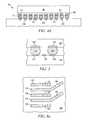
- FIGS. 1 and 2illustrate a cross-sectional view and top view of a portion of flipchip type semiconductor die 10 and interconnects or bumps 12 metallurgically and electrically connected between bump pads 18 as formed on semiconductor die 10 and trace lines 20 and 22 as formed on substrate 30 .
- Trace line 22is routed between traces lines 20 and bumps 12 on substrate 30 .
- Trace lines 20 and 22are electrical signal conductors with optional bump pads for mating to bumps 12 - 14 .
- Solder mask 26overlays trace lines 20 and 22 .
- Solder mask or registration openings (SRO) 28are formed over substrate 30 to expose trace lines 20 and 22 .
- SRO 28confines the conductive bump material on the bump pads of trace lines 20 and 22 during reflow and prevents the molten bump material from leaching onto the trace lines, which can cause electrical shorts to adjacent structures.
- SRO 28is made larger than the trace line or bump pad.
- SRO 28is typically circular in shape and made as small as possible to reduce the pitch of trace lines 20 and 22 and increase routing density.
- Dbump base diameter
- Wtrace line width
- Lthe ligament separation between SRO and adjacent structures.
- the present inventionis a method of making a semiconductor device comprising the steps of providing a semiconductor die having a plurality of die bump pad, providing a substrate having a plurality of conductive trace with an interconnect site, forming a solder mask patch interstitially between the die bump pads or interconnect sites, depositing a conductive bump material on the interconnect sites or die bump pads, mounting the semiconductor die to the substrate so that the conductive bump material is disposed between the die bump pads and interconnect sites, reflowing the conductive bump material without a solder mask around the die bump pad or interconnect site to form an interconnect structure between the semiconductor die and substrate, and depositing an encapsulant between the semiconductor die and substrate.
- the solder mask patchconfines the conductive bump material within the die bump pad or interconnect site
- the present inventionis a method of making a semiconductor device comprising the steps of providing a first semiconductor structure having a plurality of first interconnect sites, providing a second semiconductor structure having a plurality of second interconnect sites, forming a solder mask patch between the first interconnect sites or second interconnect sites, depositing a conductive bump material between the first and second interconnect sites, forming an interconnect structure from the conductive bump material to bond the first and second semiconductor structures, and depositing an encapsulant between the first and second semiconductor structures.
- the solder mask patchconfines the conductive bump material within the first interconnect sites or second interconnect sites.
- the present inventionis a method of making a semiconductor device comprising the steps of providing a first semiconductor structure having a plurality of first interconnect sites, providing a second semiconductor structure having a plurality of second interconnect sites, forming a solder mask patch between the first interconnect sites or second interconnect sites, and forming an interconnect structure to bond the first and second semiconductor structures.
- the solder mask patchconfines the interconnect structure within the first interconnect sites or second interconnect sites.
- the present inventionis a semiconductor device comprising a first semiconductor structure having a plurality of first interconnect sites and second semiconductor structure having a plurality of second interconnect sites.
- a solder mask patchis formed between the first interconnect sites or second interconnect sites.
- An interconnect structurebonding the first and second semiconductor structures.
- the solder mask patchconfines the interconnect structure within the first interconnect sites or second interconnect sites.
- An encapsulantis deposited between the first and second semiconductor structures.
- FIG. 1illustrates a cross-sectional view of conventional interconnects formed between a semiconductor die and trace lines on a substrate;
- FIG. 2illustrates a top view of conventional interconnects formed over the trace lines through solder mask openings
- FIG. 3illustrates a PCB with different types of packages mounted to its surface
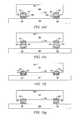
- FIGS. 4 a - 4 dillustrate further detail of the representative semiconductor packages mounted to the PCB
- FIG. 5illustrates interconnects formed between a semiconductor die and trace lines on a substrate
- FIGS. 6 a - 6 cillustrate integrated bump pads along the trace lines
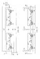
- FIG. 7illustrates a solder mask patch formed interstitially within the array of integrated bump pads on the substrate
- FIG. 8illustrates bumps formed on the integrated bump pads with bump material confined by the solder mask patch during reflow
- FIGS. 9 a - 9 hillustrate various interconnect structures formed over a semiconductor die for bonding to conductive traces on a substrate
- FIGS. 10 a - 10 gillustrate the semiconductor die and interconnect structure bonded to the conductive traces
- FIGS. 11 a - 11 dillustrate the semiconductor die with a wedge-shaped interconnect structure bonded to the conductive traces
- FIGS. 12 a - 12 dillustrate another embodiment of the semiconductor die and interconnect structure bonded to the conductive traces
- FIGS. 13 a - 13 cillustrate stepped bump and stud bump interconnect structures bonded to the conductive traces
- FIGS. 14 a - 14 billustrate conductive traces with conductive vias
- FIGS. 15 a - 15 cillustrate mold underfill between the semiconductor die and substrate
- FIG. 16illustrates another mold underfill between the semiconductor die and substrate
- FIG. 17illustrates the semiconductor die and substrate after mold underfill
- FIGS. 18 a - 18 cillustrate various arrangements of the conductive traces with open solder registration
- FIG. 19illustrates a POP with masking layer dam to restrain the encapsulant during mold underfill.
- Front-end manufacturinginvolves the formation of a plurality of die on the surface of a semiconductor wafer.
- Each die on the wafercontains active and passive electrical components, which are electrically connected to form functional electrical circuits.
- Active electrical componentssuch as transistors and diodes, have the ability to control the flow of electrical current.
- Passive electrical componentssuch as capacitors, inductors, resistors, and transformers, create a relationship between voltage and current necessary to perform electrical circuit functions.
- Passive and active componentsare formed over the surface of the semiconductor wafer by a series of process steps including doping, deposition, photolithography, etching, and planarization.
- Dopingintroduces impurities into the semiconductor material by techniques such as ion implantation or thermal diffusion.
- the doping processmodifies the electrical conductivity of semiconductor material in active devices, transforming the semiconductor material into an insulator, conductor, or dynamically changing the semiconductor material conductivity in response to an electric field or base current.
- Transistorscontain regions of varying types and degrees of doping arranged as necessary to enable the transistor to promote or restrict the flow of electrical current upon the application of the electric field or base current.
- Active and passive componentsare formed by layers of materials with different electrical properties.
- the layerscan be formed by a variety of deposition techniques determined in part by the type of material being deposited. For example, thin film deposition may involve chemical vapor deposition (CVD), physical vapor deposition (PVD), electrolytic plating, and electroless plating processes.
- CVDchemical vapor deposition
- PVDphysical vapor deposition
- electrolytic platingelectroless plating processes.
- Each layeris generally patterned to form portions of active components, passive components, or electrical connections between components.
- the layerscan be patterned using photolithography, which involves the deposition of light sensitive material, e.g., photoresist, over the layer to be patterned.
- a patternis transferred from a photomask to the photoresist using light.
- the portion of the photoresist pattern subjected to lightis removed using a solvent, exposing portions of the underlying layer to be patterned.
- the remainder of the photoresistis removed, leaving behind a patterned layer.
- some types of materialsare patterned by directly depositing the material into the areas or voids formed by a previous deposition/etch process using techniques such as electroless and electrolytic plating.
- Planarizationcan be used to remove material from the surface of the wafer and produce a uniformly flat surface. Planarization involves polishing the surface of the wafer with a polishing pad. An abrasive material and corrosive chemical are added to the surface of the wafer during polishing. The combined mechanical action of the abrasive and corrosive action of the chemical removes any irregular topography, resulting in a uniformly flat surface.
- Back-end manufacturingrefers to cutting or singulating the finished wafer into the individual die and then packaging the die for structural support and environmental isolation.
- the waferis scored and broken along non-functional regions of the wafer called saw streets or scribes.
- the waferis singulated using a laser cutting tool or saw blade.
- the individual dieare mounted to a package substrate that includes pins or contact pads for interconnection with other system components.
- Contact pads formed over the semiconductor dieare then connected to contact pads within the package.
- the electrical connectionscan be made with solder bumps, stud bumps, conductive paste, or wirebonds.
- An encapsulant or other molding materialis deposited over the package to provide physical support and electrical isolation.
- the finished packageis then inserted into an electrical system and the functionality of the semiconductor device is made available to the other system components.
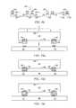
- FIG. 3illustrates electronic device 50 having a chip carrier substrate or printed circuit board (PCB) 52 with a plurality of semiconductor packages mounted on its surface.
- Electronic device 50may have one type of semiconductor package, or multiple types of semiconductor packages, depending on the application. The different types of semiconductor packages are shown in FIG. 3 for purposes of illustration.
- Electronic device 50may be a stand-alone system that uses the semiconductor packages to perform one or more electrical functions.
- electronic device 50may be a subcomponent of a larger system.
- electronic device 50may be part of a cellular phone, personal digital assistant (PDA), digital video camera (DVC), or other electronic communication device.
- PDApersonal digital assistant
- DVCdigital video camera
- electronic device 50can be a graphics card, network interface card, or other signal processing card that can be inserted into a computer.
- the semiconductor packagecan include microprocessors, memories, application specific integrated circuits (ASIC), logic circuits, analog circuits, RF circuits, discrete devices, or other semiconductor die or electrical components.
- ASICapplication specific integrated circuits
- the miniaturization and the weight reductionare essential for these products to be accepted by the market.
- the distance between semiconductor devicesmust be decreased to achieve higher density.
- PCB 52provides a general substrate for structural support and electrical interconnect of the semiconductor packages mounted on the PCB.
- Conductive signal traces 54are formed over a surface or within layers of PCB 52 using evaporation, electrolytic plating, electroless plating, screen printing, or other suitable metal deposition process. Signal traces 54 provide for electrical communication between each of the semiconductor packages, mounted components, and other external system components. Traces 54 also provide power and ground connections to each of the semiconductor packages.
- a semiconductor devicehas two packaging levels.
- First level packagingis a technique for mechanically and electrically attaching the semiconductor die to an intermediate carrier.
- Second level packaginginvolves mechanically and electrically attaching the intermediate carrier to the PCB.
- a semiconductor devicemay only have the first level packaging where the die is mechanically and electrically mounted directly to the PCB.
- first level packagingincluding wire bond package 56 and flip chip 58
- second level packagingincluding ball grid array (BGA) 60 , bump chip carrier (BCC) 62 , dual in-line package (DIP) 64 , land grid array (LGA) 66 , multi-chip module (MCM) 68 , quad flat non-leaded package (QFN) 70 , and quad flat package 72 .
- BGAball grid array
- BCCbump chip carrier
- DIPdual in-line package
- LGAland grid array
- MCMmulti-chip module
- QFNquad flat non-leaded package
- quad flat package 72quad flat package
- electronic device 50includes a single attached semiconductor package, while other embodiments call for multiple interconnected packages.
- manufacturerscan incorporate pre-made components into electronic devices and systems. Because the semiconductor packages include sophisticated functionality, electronic devices can be manufactured using cheaper components and a streamlined manufacturing process. The resulting devices are less likely to fail and less expensive to manufacture resulting in a lower cost for consumers.
- FIGS. 4 a - 4 cshow exemplary semiconductor packages.
- FIG. 4 aillustrates further detail of DIP 64 mounted on PCB 52 .
- Semiconductor die 74includes an active region containing analog or digital circuits implemented as active devices, passive devices, conductive layers, and dielectric layers formed within the die and are electrically interconnected according to the electrical design of the die.
- the circuitmay include one or more transistors, diodes, inductors, capacitors, resistors, and other circuit elements formed within the active region of semiconductor die 74 .
- Contact pads 76are one or more layers of conductive material, such as aluminum (Al), copper (Cu), tin (Sn), nickel (Ni), gold (Au), or silver (Ag), and are electrically connected to the circuit elements formed within semiconductor die 74 .
- semiconductor die 74is mounted to an intermediate carrier 78 using a gold-silicon eutectic layer or adhesive material such as thermal epoxy or epoxy resin.
- the package bodyincludes an insulative packaging material such as polymer or ceramic.
- Conductor leads 80 and wire bonds 82provide electrical interconnect between semiconductor die 74 and PCB 52 .
- Encapsulant 84is deposited over the package for environmental protection by preventing moisture and particles from entering the package and contaminating die 74 or wire bonds 82 .
- FIG. 4 billustrates further detail of BCC 62 mounted on PCB 52 .
- Semiconductor die 88is mounted over carrier 90 using an underfill or epoxy-resin adhesive material 92 .
- Wire bonds 94provide first level packaging interconnect between contact pads 96 and 98 .
- Molding compound or encapsulant 100is deposited over semiconductor die 88 and wire bonds 94 to provide physical support and electrical isolation for the device.
- Contact pads 102are formed over a surface of PCB 52 using a suitable metal deposition process such as electrolytic plating or electroless plating to prevent oxidation.
- Contact pads 102are electrically connected to one or more conductive signal traces 54 in PCB 52 .
- Bumps 104are formed between contact pads 98 of BCC 62 and contact pads 102 of PCB 52 .
- semiconductor die 58is mounted face down to intermediate carrier 106 with a flip chip style first level packaging.
- Active region 108 of semiconductor die 58contains analog or digital circuits implemented as active devices, passive devices, conductive layers, and dielectric layers formed according to the electrical design of the die.
- the circuitmay include one or more transistors, diodes, inductors, capacitors, resistors, and other circuit elements within active region 108 .
- Semiconductor die 58is electrically and mechanically connected to carrier 106 through bumps 110 .
- BGA 60is electrically and mechanically connected to PCB 52 with a BGA style second level packaging using bumps 112 .
- Semiconductor die 58is electrically connected to conductive signal traces 54 in PCB 52 through bumps 110 , signal lines 114 , and bumps 112 .
- a molding compound or encapsulant 116is deposited over semiconductor die 58 and carrier 106 to provide physical support and electrical isolation for the device.
- the flip chip semiconductor deviceprovides a short electrical conduction path from the active devices on semiconductor die 58 to conduction tracks on PCB 52 in order to reduce signal propagation distance, lower capacitance, and improve overall circuit performance.
- the semiconductor die 58can be mechanically and electrically connected directly to PCB 52 using flip chip style first level packaging without intermediate carrier 106 .
- active area 108 of semiconductor die 58is directly mounted facedown to PCB 115 , i.e., without an intermediate carrier, as shown in FIG. 4 d .
- Bump pads 111are formed on active area 108 using an evaporation, electrolytic plating, electroless plating, screen printing, or other suitable metal deposition process. Bump pads 111 connect to the active and passive circuits by conduction tracks in active area 108 . Bump pads 111 can be Al, Sn, Ni, Au, Ag, or Cu.
- An electrically conductive bump materialis deposited over bump pads 111 or conduction tracks 118 in PCB 115 using an evaporation, electrolytic plating, electroless plating, ball drop, or screen printing process.
- the bump materialcan be Al, Sn, Ni, Au, Ag, lead (Pb), Bi, Cu, solder, and combinations thereof, with an optional flux material.
- the bump materialcan be eutectic Sn/Pb, high-lead solder, or lead-free solder.
- the bump materialis bonded between die bump pads 111 and conduction tracks 118 on PCB 115 using a suitable attachment or bonding process.
- the bump materialis reflowed by heating the material above its melting point to form spherical balls or bumps 117 .
- the flip chip semiconductor deviceprovides a short electrical conduction path from the active devices on semiconductor die 58 to conduction tracks 118 on PCB 115 in order to reduce signal propagation, lower capacitance, and achieve overall better circuit performance.
- FIG. 5illustrates a cross-sectional view of a portion of flipchip type semiconductor die 120 with bump pads 122 .
- Trace lines 130 and 132are formed on substrate 136 .
- Trace lines 130 and 132are straight electrical conductors with integrated bump pads 138 , as shown in FIG. 6 a .
- the integrated bump pads 138are co-linear with trace lines 130 and 132 .
- trace lines 130 and 132can have round integrated bump pads 139 , as shown in FIG. 6 b , or rectangular integrated bump pads 140 , as shown in FIG. 6 c .
- the integrated bump padsare typically arranged in an array for maximum interconnect density and capacity.
- solder mask 142is deposited over a portion of trace lines 130 and 132 .
- solder mask 142is not formed over integrated bump pads 138 . Consequently, there is no SRO for each bump pad on the substrate, as found in prior art FIG. 2 .
- a non-wettable solder mask patch 144is formed on substrate 136 interstitially within the array of integrated bump pads 138 , i.e., between adjacent bump pads.
- the solder mask patchcan also be formed on semiconductor die 10 interstitially within the array of die bump pads 122 . More generally, the solder mask patch is formed in close proximity to the integrated bump pads in any arrangement to prevent run-out to less wettable areas.
- FIG. 8shows bumps 150 and 152 formed over integrated bump pads 138 and confined by solder mask patch 144 .
- An electrically conductive bump materialis deposited over die bump pads 122 or integrated bump pads 138 using an evaporation, electrolytic plating, electroless plating, ball drop, or screen printing process.
- the bump materialcan be Al, Sn, Ni, Au, Ag, Pb, Bi, Cu, solder, and combinations thereof, with an optional flux solution.
- the bump materialcan be eutectic Sn/Pb, high-lead solder, or lead-free solder.
- the bump materialis bonded to integrated bump pads 138 using a suitable attachment or bonding process. In one embodiment, the bump material is reflowed by heating the material above its melting point to form spherical balls or bumps 150 and 152 .
- bumps 150 and 152are reflowed a second time to improve electrical contact to die bump pads 122 and integrated bump pads 138 .
- the bumpscan also be compression bonded to die bump pads 122 and integrated bump pads 138 .
- Bumps 150 and 152represent one type of interconnect structure that can be formed over integrated bump pads 138 .
- the interconnect structurecan also use stud bump, micro bump, or other electrical interconnect.
- solder mask 142may be formed over a portion of trace lines 130 and 132 and substrate 136 away from integrated bump pads 138 , as shown in FIG. 7 . However, solder mask 142 is not formed over integrated bump pads 138 . That is, the portion of trace lines 130 and 132 designed to mate with the bump material is devoid of an SRO formed in solder mask 142 .
- solder mask patch 144is formed on substrate 136 interstitially within the array of integrated bump pads 138 .
- Solder mask patch 144is non-wettable material.
- Solder mask patch 144can be the same material as solder mask 142 and applied during the same processing step, or a different material during a different processing step.
- Solder mask patch 144can be formed by selective oxidation, plating, or other treatment of the portion of the trace or pad within the array of integrated bump pads 138 .
- Solder mask patch 144confines solder flow to integrated bump pads 138 and prevents leaching of conductive bump material to adjacent structures.
- the wetting and surface tensioncauses the bump material to be confined and retained within the space between die bump pads 122 and integrated bump pads 138 and portion of substrate 136 immediately adjacent to trace lines 130 and 132 and substantially within the footprint of the integrated bump pads 138 .
- the bump materialcan be immersed in a flux solution prior to placement on die bump pad 122 or integrated bump pads 138 to selectively render the region contacted by the bump material more wettable than the surrounding area of trace lines 130 and 132 .
- the molten bump materialremains confined substantially within the area defined by the bump pads due to the wettable properties of the flux solution.
- the bump materialdoes not run-out to the less wettable areas.
- a thin oxide layer or other insulating layercan be formed over areas where bump material is not intended to make the area less wettable.
- solder mask 142is not needed around die bump pads 122 or integrated bump pads 138 .
- trace lines 130 and 132can be formed with a finer pitch, i.e., trace lines 130 and 132 can be disposed closer to adjacent structures without making contact and forming electrical shorts.
- the minimum escape pitch of trace lines 130 and 132is 65 ⁇ m.
- the bump formationeliminates the need to account for the ligament spacing of solder mask material between adjacent openings and minimum resolvable SRO, as found in the prior art.
- FIGS. 9-14describe other embodiments with various interconnect structures applicable to the interconnect structure formed with the solder mask patch, as described in FIGS. 5-8 .
- FIG. 9 ashows a semiconductor wafer 220 with a base substrate material 222 , such as silicon, germanium, gallium arsenide, indium phosphide, or silicon carbide, for structural support.
- a plurality of semiconductor die or components 224is formed on wafer 220 separated by saw streets 226 as described above.
- FIG. 9 bshows a cross-sectional view of a portion of semiconductor wafer 220 .
- Each semiconductor die 224has a back surface 228 and active surface 230 containing analog or digital circuits implemented as active devices, passive devices, conductive layers, and dielectric layers formed within the die and electrically interconnected according to the electrical design and function of the die.
- the circuitmay include one or more transistors, diodes, and other circuit elements formed within active surface 230 to implement analog circuits or digital circuits, such as digital signal processor (DSP), ASIC, memory, or other signal processing circuit.
- DSPdigital signal processor
- Semiconductor die 224may also contain integrated passive devices (IPDs), such as inductors, capacitors, and resistors, for RF signal processing.
- IPDsintegrated passive devices
- semiconductor die 224is a flipchip type semiconductor die.
- An electrically conductive layer 232is formed over active surface 230 using PVD, CVD, electrolytic plating, electroless plating process, or other suitable metal deposition process.
- Conductive layer 232can be one or more layers of Al, Cu, Sn, Ni, Au, Ag, or other suitable electrically conductive material.
- Conductive layer 232operates as contact pads or die bumps pads electrically connected to the circuits on active surface 230 .
- FIG. 9 cshows a portion of semiconductor wafer 220 with an interconnect structure formed over contact pads 232 .
- An electrically conductive bump material 234is deposited over contact pads 232 using an evaporation, electrolytic plating, electroless plating, ball drop, or screen printing process.
- Bump material 234can be Al, Sn, Ni, Au, Ag, Pb, Bi, Cu, solder, and combinations thereof, with an optional flux solution.
- bump material 234can be eutectic Sn/Pb, high-lead solder, or lead-free solder.
- Bump material 234is generally compliant and undergoes plastic deformation greater than about 25 ⁇ m under a force equivalent to a vertical load of about 200 grams.
- Bump material 234is bonded to contact pad 232 using a suitable attachment or bonding process.
- bump material 234can be compression bonded to contact pad 232 .
- Bump material 234can also be reflowed by heating the material above its melting point to form spherical balls or bumps 236 , as shown in FIG. 9 d .
- bumps 236are reflowed a second time to improve electrical connection to contact pad 232 .
- Bumps 236represent one type of interconnect structure that can be formed over contact pad 232 .
- the interconnect structurecan also use stud bump, micro bump, or other electrical interconnect.
- FIG. 9 eshows another embodiment of the interconnect structure formed over contact pads 232 as composite bumps 238 including a non-fusible or non-collapsible portion 240 and fusible or collapsible portion 242 .
- the fusible or collapsible and non-fusible or non-collapsible attributesare defined for bumps 238 with respect to reflow conditions.
- the non-fusible portion 240can be Au, Cu, Ni, high-lead solder, or lead-tin alloy.
- the fusible portion 242can be Sn, lead-free alloy, Sn—Ag alloy, Sn—Ag—Cu alloy, Sn—Ag-indium (In) alloy, eutectic solder, tin alloys with Ag, Cu, or Pb, or other relatively low temperature melt solder.
- the non-fusible portion 240is about 45 ⁇ m in height and fusible portion 242 is about 35 ⁇ m in height.
- FIG. 9 fshows another embodiment of the interconnect structure formed over contact pads 232 as bump 244 over conductive pillar 246 .
- Bump 244is fusible or collapsible and conductive pillar 246 is non-fusible or non-collapsible.
- the fusible or collapsible and non-fusible or non-collapsible attributesare defined with respect to reflow conditions.
- Bump 244can be Sn, lead-free alloy, Sn—Ag alloy, Sn—Ag—Cu alloy, Sn—Ag—In alloy, eutectic solder, tin alloys with Ag, Cu, or Pb, or other relatively low temperature melt solder.
- Conductive pillar 246can be Au, Cu, Ni, high-lead solder, or lead-tin alloy.
- conductive pillar 246is a Cu pillar and bump 244 is a solder cap. Given a contact pad 232 width or diameter of 100 ⁇ m, conductive pillar 246 is about 45 ⁇ m in height and bump 244 is about 35 ⁇ m in height.
- FIG. 9 gshows another embodiment of the interconnect structure formed over contact pads 232 as bump material 248 with asperities 250 .
- Bump material 248is soft and deformable under reflow conditions with a low yield strength and high elongation to failure, similar to bump material 234 .
- Asperities 250are formed with a plated surface finish and are shown exaggerated in the figures for purposes of illustration. The scale of asperities 250 is generally in the order about 1-25 ⁇ m. The asperities can also be formed on bump 236 , composite bump 238 , and bump 244 .
- semiconductor wafer 220is singulated through saw street 226 using a saw blade or laser cutting tool 252 into individual semiconductor die 224 .
- FIG. 10 ashows a substrate or PCB 254 with conductive trace 256 .
- Substrate 254can be a single-sided FR5 laminate or 2-sided BT-resin laminate.
- Semiconductor die 224is positioned so that bump material 234 is aligned with an interconnect site on conductive trace 256 , see FIGS. 6 a - 6 c , 7 - 8 , and 18 a - 18 c .
- bump material 234can be aligned with a conductive pad or other interconnect site formed on substrate 254 .
- Bump material 234is wider than conductive trace 256 .
- bump material 234has a width of less than 100 ⁇ m and conductive trace or pad 256 has a width of 35 ⁇ m for a bump pitch of 150 ⁇ m.
- Conductive traces 256is applicable to the interconnect structure formed with the solder mask patch, as described in FIGS. 5-8 .
- a pressure or force Fis applied to back surface 228 of semiconductor die 224 to press bump material 234 onto conductive trace 256 .
- the force Fcan be applied with an elevated temperature. Due to the compliant nature of bump material 234 , the bump material deforms or extrudes around the top surface and side surfaces of conductive trace 256 , referred to as BOL. In particular, the application of pressure causes bump material 234 to undergo a plastic deformation greater than about 25 ⁇ m under force F equivalent to a vertical load of about 200 grams and cover the top surface and side surfaces of the conductive trace, as shown in FIG. 10 b . Bump material 234 can also be metallurgically connected to conductive trace 256 by bringing the bump material in physical contact with the conductive trace and then reflowing the bump material under a reflow temperature.
- the conductive trace pitchcan be reduced to increase routing density and I/O count.
- the narrower conductive trace 256reduces the force F needed to deform bump material 234 around the conductive trace.
- the requisite force Fmay be 30-50% of the force needed to deform bump material against a conductive trace or pad that is wider than the bump material.
- the lower compressive force Fis useful for fine pitch interconnect and small die to maintain coplanarity with a specified tolerance and achieve uniform z-direction deformation and high reliability interconnect union.
- deforming bump material 234 around conductive trace 256mechanically locks the bump to the trace to prevent die shifting or die floating during reflow.
- FIG. 10 cshows bump 236 formed over contact pad 232 of semiconductor die 224 .
- Semiconductor die 224is positioned so that bump 236 is aligned with an interconnect site on conductive trace 256 .
- bump 236can be aligned with a conductive pad or other interconnect site formed on substrate 254 .
- Bump 236is wider than conductive trace 256 .
- Conductive traces 256is applicable to the interconnect structure formed with the solder mask patch, as described in FIGS. 5-8 .
- a pressure or force Fis applied to back surface 228 of semiconductor die 224 to press bump 236 onto conductive trace 256 .
- the force Fcan be applied with an elevated temperature. Due to the compliant nature of bump 236 , the bump deforms or extrudes around the top surface and side surfaces of conductive trace 256 . In particular, the application of pressure causes bump material 236 to undergo a plastic deformation and cover the top surface and side surfaces of conductive trace 256 . Bump 236 can also be metallurgically connected to conductive trace 256 by bringing the bump in physical contact with the conductive trace under reflow temperature.
- the conductive trace pitchcan be reduced to increase routing density and I/O count.
- the narrower conductive trace 256reduces the force F needed to deform bump 236 around the conductive trace.
- the requisite force Fmay be 30-50% of the force needed to deform a bump against a conductive trace or pad that is wider than the bump.
- the lower compressive force Fis useful for fine pitch interconnect and small die to maintain coplanarity within a specified tolerance and achieve uniform z-direction deformation and high reliability interconnect union.
- deforming bump 236 around conductive trace 256mechanically locks the bump to the trace to prevent die shifting or die floating during reflow.
- FIG. 10 dshows composite bump 238 formed over contact pad 232 of semiconductor die 224 .
- Semiconductor die 224is positioned so that composite bump 238 is aligned with an interconnect site on conductive trace 256 .
- composite bump 238can be aligned with a conductive pad or other interconnect site formed on substrate 254 .
- Composite bump 238is wider than conductive trace 256 .
- Conductive traces 256is applicable to the interconnect structure formed with the solder mask patch, as described in FIGS. 5-8 .
- a pressure or force Fis applied to back surface 228 of semiconductor die 224 to press fusible portion 242 onto conductive trace 256 .
- the force Fcan be applied with an elevated temperature. Due to the compliant nature of fusible portion 242 , the fusible portion deforms or extrudes around the top surface and side surfaces of conductive trace 256 . In particular, the application of pressure causes fusible portion 242 to undergo a plastic deformation and cover the top surface and side surfaces of conductive trace 256 .
- Composite bump 238can also be metallurgically connected to conductive trace 256 by bringing fusible portion 242 in physical contact with the conductive trace under reflow temperature.
- the non-fusible portion 240does not melt or deform during the application of pressure or temperature and retains its height and shape as a vertical standoff between semiconductor die 224 and substrate 254 .
- the additional displacement between semiconductor die 224 and substrate 254provides greater coplanarity tolerance between the mating surfaces.
- the height or volume of fusible bump material in relation to the non-fusible base materialis selected to ensure confinement by virtue of surface tension forces. During reflow, the fusible base material is confined around the non-fusible base material due to the solder mask patch. The fusible bump material around the non-fusible base also maintains die placement during reflow.
- the height of the composite interconnectis the same or less than the diameter of the bump. In some cases, the height of the composite interconnect is greater than the diameter of the interconnect. In one embodiment, given a bump base diameter of 100 ⁇ m, the non-fusible base is about 45 ⁇ m in height and the fusible cap is about 35 ⁇ m in height.
- the molten bump materialremains confined substantially within the area defined by the bump pads due to the solder mask patch and because the volume of bump material deposited to form the composite bump, including non-fusible base and fusible cap, is selected so that the resulting surface tension is sufficient to retain the bump material substantially within the footprint of the bump pads and prevent run-out to unintended adjacent or nearby areas.
- the solder mask patch formed interstitially with the array of bump padsreduces trace line pitch and increases routing density.
- a large number (e.g., thousands) of composite bumps 238 on semiconductor die 224are attached to interconnect sites on conductive trace 256 of substrate 254 .
- Some of the bumps 238may fail to properly connect to conductive trace 256 , particularly if die 224 is warped.
- composite bump 238is wider than conductive trace 256 .
- the fusible portion 242deforms or extrudes around the top surface and side surfaces of conductive trace 256 and mechanically locks composite bump 238 to the conductive trace.
- the mechanical interlockis formed by nature of the fusible portion 242 being softer and more compliant than conductive trace 256 and therefore deforming over the top surface and around the side surfaces of the conductive trace for greater contact surface area.
- the mechanical interlock between composite bump 238 and conductive trace 256holds the bump to the conductive trace during reflow, i.e., the bump and conductive trace do not lose contact. Accordingly, composite bump 238 mating to conductive trace 256 reduces bump interconnect failures.
- FIG. 10 eshows conductive pillar 246 and bump 244 formed over contact pad 232 of semiconductor die 224 .
- Semiconductor die 224is positioned so that bump 244 is aligned with an interconnect site on conductive trace 256 .
- bump 244can be aligned with a conductive pad or other interconnect site formed on substrate 254 .
- Bump 244is wider than conductive trace 256 .
- Conductive traces 256is applicable to the interconnect structure formed with the solder mask patch, as described in FIGS. 5-8 .
- a pressure or force Fis applied to back surface 228 of semiconductor die 224 to press bump 244 onto conductive trace 256 .
- the force Fcan be applied with an elevated temperature. Due to the compliant nature of bump 244 , the bump deforms or extrudes around the top surface and side surfaces of conductive trace 256 . In particular, the application of pressure causes bump 244 to undergo a plastic deformation and cover the top surface and side surfaces of conductive trace 256 .
- Conductive pillar 246 and bump 244can also be metallurgically connected to conductive trace 256 by bringing the bump in physical contact with the conductive trace under reflow temperature.
- Conductive pillar 246does not melt or deform during the application of pressure or temperature and retains its height and shape as a vertical standoff between semiconductor die 224 and substrate 254 .
- the additional displacement between semiconductor die 224 and substrate 254provides greater coplanarity tolerance between the mating surfaces.
- the wider bump 244 and narrower conductive trace 256have similar low requisite compressive force and mechanical locking features and advantages described above for bump material 234 and bump 236 .
- FIG. 10 fshows bump material 248 with asperities 250 formed over contact pad 232 of semiconductor die 224 .
- Semiconductor die 224is positioned so that bump material 248 is aligned with an interconnect site on conductive trace 256 .
- bump material 248can be aligned with a conductive pad or other interconnect site formed on substrate 254 .
- Bump material 248is wider than conductive trace 256 .
- a pressure or force Fis applied to back surface 228 of semiconductor die 224 to press bump material 248 onto conductive trace 256 .
- the force Fcan be applied with an elevated temperature. Due to the compliant nature of bump material 248 , the bump deforms or extrudes around the top surface and side surfaces of conductive trace 256 .
- the application of pressurecauses bump material 248 to undergo a plastic deformation and cover the top surface and side surfaces of conductive trace 256 .
- asperities 250are metallurgically connected to conductive trace 256 . Asperities 250 are sized on the order about 1-25 ⁇ m.
- FIG. 10 gshows a substrate or PCB 258 with trapezoidal conductive trace 260 having angled or sloped sides.
- Bump material 261is formed over contact pad 232 of semiconductor die 224 .
- Semiconductor die 224is positioned so that bump material 261 is aligned with an interconnect site on conductive trace 260 .
- bump material 261can be aligned with a conductive pad or other interconnect site formed on substrate 258 .
- Bump material 261is wider than conductive trace 260 .
- Conductive traces 260is applicable to the interconnect structure formed with the solder mask patch, as described in FIGS. 5-8 .
- a pressure or force Fis applied to back surface 228 of semiconductor die 224 to press bump material 261 onto conductive trace 260 .
- the force Fcan be applied with an elevated temperature. Due to the compliant nature of bump material 261 , the bump material deforms or extrudes around the top surface and side surfaces of conductive trace 260 . In particular, the application of pressure causes bump material 261 to undergo a plastic deformation under force F to cover the top surface and the angled side surfaces of conductive trace 260 . Bump material 261 can also be metallurgically connected to conductive trace 260 by bringing the bump material in physical contact with the conductive trace and then reflowing the bump material under a reflow temperature.
- FIGS. 11 a - 11 dshow a BOL embodiment of semiconductor die 224 and elongated composite bump 262 having a non-fusible or non-collapsible portion 264 and fusible or collapsible portion 266 .
- the non-fusible portion 264can be Au, Cu, Ni, high-lead solder, or lead-tin alloy.
- the fusible portion 266can be Sn, lead-free alloy, Sn—Ag alloy, Sn—Ag—Cu alloy, Sn—Ag—In alloy, eutectic solder, tin alloys with Ag, Cu, or Pb, or other relatively low temperature melt solder.
- the non-fusible portion 264makes up a larger part of composite bump 262 than the fusible portion 266 .
- the non-fusible portion 264is fixed to contact pad 232 of semiconductor die 224 .
- Semiconductor die 224is positioned so that composite bump 262 is aligned with an interconnect site on conductive trace 268 formed on substrate 270 , as shown in FIG. 11 a .
- Composite bump 262is tapered along conductive trace 268 , i.e., the composite bump has a wedge shape, longer along a length of conductive trace 268 and narrower across the conductive trace.
- the tapered aspect of composite bump 262occurs along the length of conductive trace 268 .
- the view in FIG. 11 ashows the shorter aspect or narrowing taper co-linear with conductive trace 268 .
- the view in FIG. 11 bnormal to FIG. 11 a , shows the longer aspect of the wedge-shaped composite bump 262 .
- the shorter aspect of composite bump 262is wider than conductive trace 268 .
- the fusible portion 266collapses around conductive trace 268 upon application of pressure and/or reflow with heat, as shown in FIGS. 11 c and 11 d .
- the non-fusible portion 264does not melt or deform during reflow and retains its form and shape.
- the non-fusible portion 264can be dimensioned to provide a standoff distance between semiconductor die 224 and substrate 270 .
- a finish such as Cu OSPcan be applied to substrate 270 .
- Conductive traces 268is applicable to the interconnect structure formed with the solder mask patch, as described in FIGS. 5-8 .
- a large number (e.g., thousands) of composite bumps 262 on semiconductor die 224are attached to interconnect sites on conductive trace 268 of substrate 270 . Some of the bumps 262 may fail to properly connect to conductive trace 268 , particularly if semiconductor die 224 is warped. Recall that composite bump 262 is wider than conductive trace 268 . With a proper force applied, the fusible portion 266 deforms or extrudes around the top surface and side surfaces of conductive trace 268 and mechanically locks composite bump 262 to the conductive trace.
- the mechanical interlockis formed by nature of the fusible portion 266 being softer and more compliant than conductive trace 268 and therefore deforming around the top surface and side surfaces of the conductive trace for greater contact area.
- the wedge-shape of composite bump 262increases contact area between the bump and conductive trace, e.g., along the longer aspect of FIGS. 11 b and 11 d , without sacrificing pitch along the shorter aspect of FIGS. 11 a and 11 c .
- the mechanical interlock between composite bump 262 and conductive trace 268holds the bump to the conductive trace during reflow, i.e., the bump and conductive trace do not lose contact. Accordingly, composite bump 262 mating to conductive trace 268 reduces bump interconnect failures.
- FIGS. 12 a - 12 dshow a BOL embodiment of semiconductor die 224 with bump material 274 formed over contact pads 232 , similar to FIG. 9 c .
- bump material 274is generally compliant and undergoes plastic deformation greater than about 25 ⁇ m under a force equivalent to a vertical load of about 200 grams.
- Bump material 274is wider than conductive trace 276 on substrate 278 .
- a plurality of asperities 280is formed on conductive trace 276 with a height on the order about 1-25 ⁇ m.
- Semiconductor die 224is positioned so that bump material 274 is aligned with an interconnect site on conductive trace 276 .
- bump material 274can be aligned with a conductive pad or other interconnect site formed on substrate 278 .
- a pressure or force Fis applied to back surface 228 of semiconductor die 224 to press bump material 274 onto conductive trace 276 and asperities 280 , as shown in FIG. 12 b .
- the force Fcan be applied with an elevated temperature. Due to the compliant nature of bump material 274 , the bump material deforms or extrudes around the top surface and side surfaces of conductive trace 276 and asperities 280 .
- the application of pressurecauses bump material 274 to undergo a plastic deformation and cover the top surface and side surfaces of conductive trace 276 and asperities 280 .
- the plastic flow of bump material 274creates macroscopic mechanical interlocking points between the bump material and the top surface and side surfaces of conductive trace 276 and asperities 280 .
- the plastic flow of bump material 274occurs around the top surface and side surfaces of conductive trace 276 and asperities 280 , but does not extend excessively onto substrate 278 , which could cause electrical shorting and other defects.
- the mechanical interlock between the bump material and the top surface and side surfaces of conductive trace 276 and asperities 280provides a robust connection with greater contact area between the respective surfaces, without significantly increasing the bonding force.
- the mechanical interlock between the bump material and the top surface and side surfaces of conductive trace 276 and asperities 280also reduces lateral die shifting during subsequent manufacturing processes, such as encapsulation.
- FIG. 12 cshows another BOL embodiment with bump material 274 narrower than conductive trace 276 .
- a pressure or force Fis applied to back surface 228 of semiconductor die 224 to press bump material 274 onto conductive trace 276 and asperities 280 .
- the force Fcan be applied with an elevated temperature. Due to the compliant nature of bump material 274 , the bump material deforms or extrudes over the top surface of conductive trace 276 and asperities 280 . In particular, the application of pressure causes bump material 274 to undergo a plastic deformation and cover the top surface of conductive trace 276 and asperities 280 . The plastic flow of bump material 274 creates macroscopic mechanical interlocking points between the bump material and the top surface of conductive trace 276 and asperities 280 .
- the mechanical interlock between the bump material and the top surface of conductive trace 276 and asperities 280provides a robust connection with greater contact area between the respective surfaces, without significantly increasing the bonding force.
- the mechanical interlock between the bump material and the top surface of conductive trace 276 and asperities 280also reduces lateral die shifting during subsequent manufacturing processes, such as encapsulation.
- FIG. 12 dshows another BOL embodiment with bump material 274 formed over an edge of conductive trace 276 , i.e., part of the bump material is over the conductive trace and part of the bump material is not over the conductive trace.
- a pressure or force Fis applied to back surface 228 of semiconductor die 224 to press bump material 274 onto conductive trace 276 and asperities 280 .
- the force Fcan be applied with an elevated temperature. Due to the compliant nature of bump material 274 , the bump material deforms or extrudes over the top surface and side surfaces of conductive trace 276 and asperities 280 . In particular, the application of pressure causes bump material 274 to undergo a plastic deformation and cover the top surface and side surfaces of conductive trace 276 and asperities 280 .
- the plastic flow of bump material 274creates macroscopic mechanical interlocking between the bump material and the top surface and side surfaces of conductive trace 276 and asperities 280 .
- the mechanical interlock between the bump material and the top surface and side surfaces of conductive trace 276 and asperities 280provides a robust connection with greater contact area between the respective surfaces, without significantly increasing the bonding force.
- the mechanical interlock between the bump material and the top surface and side surfaces of conductive trace 276 and asperities 280also reduces lateral die shifting during subsequent manufacturing processes, such as encapsulation.
- FIGS. 13 a - 13 cshow a BOL embodiment of semiconductor die 224 with bump material 284 formed over contact pads 232 , similar to FIG. 9 c .
- a tip 286extends from the body of bump material 284 as a stepped bump with tip 286 narrower than the body of bump material 284 , as shown in FIG. 13 a .
- Semiconductor die 224is positioned so that bump material 284 is aligned with an interconnect site on conductive trace 288 on substrate 290 . More specifically, tip 286 is centered over an interconnect site on conductive trace 288 .
- bump material 284 and tip 286can be aligned with a conductive pad or other interconnect site formed on substrate 290 . Bump material 284 is wider than conductive trace 288 on substrate 290 .
- Conductive trace 288is generally compliant and undergoes plastic deformation greater than about 25 ⁇ m under a force equivalent to a vertical load of about 200 grams.
- a pressure or force Fis applied to back surface 228 of semiconductor die 224 to press tip 284 onto conductive trace 288 .
- the force Fcan be applied with an elevated temperature. Due to the compliant nature of conductive trace 288 , the conductive trace deforms around tip 286 , as shown in FIG. 13 b . In particular, the application of pressure causes conductive trace 288 to undergo a plastic deformation and cover the top surface and side surfaces of tip 286 .
- FIG. 13 cshows another BOL embodiment with rounded bump material 294 formed over contact pads 232 .
- a tip 296extends from the body of bump material 294 to form a stud bump with the tip narrower than the body of bump material 294 .
- Semiconductor die 224is positioned so that bump material 294 is aligned with an interconnect site on conductive trace 298 on substrate 300 . More specifically, tip 296 is centered over an interconnect site on conductive trace 298 .
- bump material 294 and tip 296can be aligned with a conductive pad or other interconnect site formed on substrate 300 . Bump material 294 is wider than conductive trace 298 on substrate 300 .
- Conductive trace 298is generally compliant and undergoes plastic deformation greater than about 25 ⁇ m under a force equivalent to a vertical load of about 200 grams.
- a pressure or force Fis applied to back surface 228 of semiconductor die 224 to press tip 296 onto conductive trace 298 .
- the force Fcan be applied with an elevated temperature. Due to the compliant nature of conductive trace 298 , the conductive trace deforms around tip 296 . In particular, the application of pressure causes conductive trace 298 to undergo a plastic deformation and cover the top surface and side surfaces of tip 296 .
- the conductive traces described in FIGS. 10 a - 10 g , 11 a - 11 d , and 12 a - 12 dcan also be compliant material as described in FIGS. 13 a - 13 c.
- FIGS. 14 a - 14 bshow a BOL embodiment of semiconductor die 224 with bump material 304 formed over contact pads 232 , similar to FIG. 9 c .
- Bump material 304is generally compliant and undergoes plastic deformation greater than about 25 ⁇ m under a force equivalent to a vertical load of about 200 grams.
- Bump material 304is wider than conductive trace 306 on substrate 308 .
- a conductive via 310is formed through conductive trace 306 with an opening 312 and conductive sidewalls 314 , as shown in FIG. 14 a .
- Conductive traces 306is applicable to the interconnect structure formed with the solder mask patch, as described in FIGS. 5-8 .
- Semiconductor die 224is positioned so that bump material 304 is aligned with an interconnect site on conductive trace 306 , see FIGS. 6 a - 6 c , 7 - 8 , and 18 a - 18 c .
- bump material 304can be aligned with a conductive pad or other interconnect site formed on substrate 308 .
- a pressure or force Fis applied to back surface 228 of semiconductor die 224 to press bump material 304 onto conductive trace 306 and into opening 312 of conductive via 310 .
- the force Fcan be applied with an elevated temperature.
- bump material 304Due to the compliant nature of bump material 304 , the bump material deforms or extrudes around the top surface and side surfaces of conductive trace 306 and into opening 312 of conductive vias 310 , as shown in FIG. 14 b .
- the application of pressurecauses bump material 304 to undergo a plastic deformation and cover the top surface and side surfaces of conductive trace 306 and into opening 312 of conductive via 310 .
- Bump material 304is thus electrically connected to conductive trace 306 and conductive sidewalls 314 for z-direction vertical interconnect through substrate 308 .
- the plastic flow of bump material 304creates a mechanical interlock between the bump material and the top surface and side surfaces of conductive trace 306 and opening 312 of conductive via 310 .
- the mechanical interlock between the bump material and the top surface and side surfaces of conductive trace 306 and opening 312 of conductive via 310provides a robust connection with greater contact area between the respective surfaces, without significantly increasing the bonding force.
- the mechanical interlock between the bump material and the top surface and side surfaces of conductive trace 306 and opening 312 of conductive via 310also reduces lateral die shifting during subsequent manufacturing processes, such as encapsulation. Since conductive via 310 is formed within the interconnect site with bump material 304 , the total substrate interconnect area is reduced.
- the conductive trace pitchcan be reduced to increase routing density and I/O count.
- the narrower conductive tracereduces the force F needed to deform the interconnect structure around the conductive trace.
- the requisite force Fmay be 30-50% of the force needed to deform a bump against a conductive trace or pad that is wider than the bump.
- the lower compressive force Fis useful for fine pitch interconnect and small die to maintain coplanarity within a specified tolerance and achieve uniform z-direction deformation and high reliability interconnect union.
- deforming the interconnect structure around the conductive tracemechanically locks the bump to the trace to prevent die shifting or die floating during reflow.
- FIGS. 15 a - 15 cshow a mold underfill (MUF) process to deposit encapsulant around the bumps between the semiconductor die and substrate.
- FIG. 15 ashows semiconductor die 224 mounted to substrate 254 using bump material 234 from FIG. 10 b and placed between upper mold support 316 and lower mold support 318 of chase mold 320 .
- the other semiconductor die and substrate combinations from FIGS. 10 a - 10 g , 11 a - 11 d , 12 a - 12 d , 13 a - 13 c , and 14 a - 14 bcan be placed between upper mold support 316 and lower mold support 318 of chase mold 320 .
- the upper mold support 316includes compressible releasing film 322 .
- upper mold support 316 and lower mold support 318are brought together to enclose semiconductor die 224 and substrate 254 with an open space over the substrate and between the semiconductor die and substrate.
- Compressible releasing film 322conforms to back surface 228 and side surfaces of semiconductor die 224 to block formation of encapsulant on these surfaces.
- An encapsulant 324 in a liquid stateis injected into one side of chase mold 320 with nozzle 326 while an optional vacuum assist 328 draws pressure from the opposite side to uniformly fill the open space over substrate 254 and the open space between semiconductor die 224 and substrate 254 with the encapsulant.
- Encapsulant 324can be polymer composite material, such as epoxy resin with filler, epoxy acrylate with filler, or polymer with proper filler.
- Encapsulant 324is non-conductive and environmentally protects the semiconductor device from external elements and contaminants. Compressible material 322 prevents encapsulant 324 from flowing over back surface 228 and around the side surfaces of semiconductor die 224 . Encapsulant 324 is cured. The back surface 228 and side surfaces of semiconductor die 224 remain exposed from encapsulant 324 .
- FIG. 15 cshows an embodiment of MUF and mold overfill (MOF), i.e., without compressible material 322 .
- Semiconductor die 224 and substrate 254are placed between upper mold support 316 and lower mold support 318 of chase mold 320 .
- the upper mold support 316 and lower mold support 318are brought together to enclose semiconductor die 224 and substrate 254 with an open space over the substrate, around the semiconductor die, and between the semiconductor die and substrate.
- Encapsulant 324 in a liquid stateis injected into one side of chase mold 320 with nozzle 326 while an optional vacuum assist 328 draws pressure from the opposite side to uniformly fill the open space around semiconductor die 224 and over substrate 254 and the open space between semiconductor die 224 and substrate 254 with the encapsulant.
- Encapsulant 324is cured.
- FIG. 16shows another embodiment of depositing encapsulant around semiconductor die 224 and in the gap between semiconductor die 224 and substrate 254 .
- Semiconductor die 224 and substrate 254are enclosed by dam 330 .
- Encapsulant 332is dispensed from nozzles 334 in a liquid state into dam 330 to fill the open space over substrate 254 and the open space between semiconductor die 224 and substrate 254 .
- the volume of encapsulant 332 dispensed from nozzles 334is controlled to fill dam 330 without covering back surface 228 or the side surfaces of semiconductor die 224 .
- Encapsulant 332is cured.
- FIG. 17shows semiconductor die 224 and substrate 254 after the MUF process from FIGS. 16 a , 16 c , and 17 .
- Encapsulant 324is uniformly distributed over substrate 254 and around bump material 234 between semiconductor die 224 and substrate 254 .
- FIGS. 18 a - 18 cshow top views of various conductive trace layouts on substrate or PCB 340 .
- conductive trace 342is a straight conductor with integrated bump pad or interconnect site 344 formed on substrate 340 .
- the sides of substrate bump pad 344can be co-linear with conductive trace 342 .
- SROis typically formed over the interconnect site to contain the bump material during reflow.
- the SROincreases interconnect pitch and reduces I/O count.
- masking layer 346can be formed over a portion of substrate 340 ; however, the masking layer is not formed around substrate bump pad 344 of conductive trace 342 . That is, the portion of conductive trace 342 designed to mate with the bump material is devoid of any SRO of masking layer 346 that would have been used for bump containment during reflow.
- Semiconductor die 224is placed over substrate 340 and the bump material is aligned with substrate bump pads 344 .
- the bump materialis electrically and metallurgically connected to substrate bump pads 344 by bringing the bump material in physical contact with the bump pad and then reflowing the bump material under a reflow temperature.
- an electrically conductive bump materialis deposited over substrate bump pad 344 using an evaporation, electrolytic plating, electroless plating, ball drop, or screen printing process.
- the bump materialcan be Al, Sn, Ni, Au, Ag, Pb, Bi, Cu, solder, and combinations thereof, with an optional flux solution.
- the bump materialcan be eutectic Sn/Pb, high-lead solder, or lead-free solder.
- the bump materialis bonded to substrate bump pad 344 using a suitable attachment or bonding process.
- the bump materialis reflowed by heating the material above its melting point to form bump or interconnect 348 , as shown in FIG. 18 b .
- bump 348is reflowed a second time to improve electrical contact to substrate bump pad 344 .
- the bump material around the narrow substrate bump pad 344maintains die placement during reflow.
- escape pitch of conductive traces 342In high routing density applications, it is desirable to minimize escape pitch of conductive traces 342 .
- the escape pitch between conductive traces 342can be reduced by eliminating the masking layer for the purpose of reflow containment, i.e., by reflowing the bump material without a masking layer. Since no SRO is formed around die bump pad 232 or substrate bump pad 344 , conductive traces 342 can be formed with a finer pitch, i.e., conductive trace 342 can be disposed closer together or to nearby structures.
- the minimum escape pitch of conductive trace 342is 125 ⁇ m .
- the mask-less bump formationeliminates the need to account for the ligament spacing of masking material between adjacent openings, solder mask registration tolerance (SRT), and minimum resolvable SRO, as found in the prior art.
- the wetting and surface tensioncauses the bump material to maintain self-confinement and be retained within the space between die bump pad 232 and substrate bump pad 344 and portion of substrate 340 immediately adjacent to conductive trace 342 substantially within the footprint of the bump pads.
- the bump materialcan be immersed in a flux solution prior to placement on die bump pad 232 or substrate bump pad 344 to selectively render the region contacted by the bump material more wettable than the surrounding area of conductive traces 342 .
- the molten bump materialremains confined substantially within the area defined by the bump pads due to the wettable properties of the flux solution.
- the bump materialdoes not run-out to the less wettable areas.
- a thin oxide layer or other insulating layercan be formed over areas where bump material is not intended to make the area less wettable. Hence, masking layer 340 is not needed around die bump pad 232 or substrate bump pad 344 .
- FIG. 18 cshows another embodiment of parallel conductive traces 352 as a straight conductor with integrated rectangular bump pad or interconnect site 354 formed on substrate 350 .
- substrate bump pad 354is wider than conductive trace 352 , but less than the width of the mating bump.
- the sides of substrate bump pad 354can be parallel to conductive trace 352 .
- Masking layer 356can be formed over a portion of substrate 350 ; however, the masking layer is not formed around substrate bump pad 354 of conductive trace 352 . That is, the portion of conductive trace 352 designed to mate with the bump material is devoid of any SRO of masking layer 356 that would have been used for bump containment during reflow.
- FIG. 19shows package-on-package (PoP) 405 with semiconductor die 406 stacked over semiconductor die 408 using die attach adhesive 410 .
- Semiconductor die 406 and 408each have an active surface containing analog or digital circuits implemented as active devices, passive devices, conductive layers, and dielectric layers formed within the die and electrically interconnected according to the electrical design and function of the die.
- the circuitmay include one or more transistors, diodes, and other circuit elements formed within the active surface to implement analog circuits or digital circuits, such as DSP, ASIC, memory, or other signal processing circuit.
- IPDssuch as inductors, capacitors, and resistors, for RF signal processing.
- Semiconductor die 406is mounted to conductive traces 412 formed on substrate 414 using bump material 416 formed on contact pads 418 , using any of the embodiments from FIGS. 10 a - 10 g , 11 a - 11 d , 12 a - 12 d , 13 a - 13 c , and 14 a - 14 b .
- Conductive traces 412is applicable to the interconnect structure formed with the solder mask patch, as described in FIGS. 5-8 .
- Semiconductor die 408is electrically connected to contact pads 420 formed on substrate 414 using bond wires 422 . The opposite end of bond wire 422 is bonded to contact pads 424 on semiconductor die 406 .
- Masking layer 426is formed over substrate 414 and opened beyond the footprint of semiconductor die 406 . While masking layer 426 does not confine bump material 416 to conductive traces 412 during reflow, the open mask can operate as a dam to prevent encapsulant 428 from migrating to contact pads 420 or bond wires 422 during MUF. Encapsulant 428 is deposited between semiconductor die 408 and substrate 414 , similar to FIGS. 15 a - 15 c . Masking layer 426 blocks MUF encapsulant 428 from reaching contact pads 420 and bond wires 422 , which could cause a defect. Masking layer 426 allows a larger semiconductor die to be placed on a given substrate without risk of encapsulant 428 bleeding onto contact pads 420 .
Landscapes
- Engineering & Computer Science (AREA)
- Microelectronics & Electronic Packaging (AREA)
- Computer Hardware Design (AREA)
- Power Engineering (AREA)
- Physics & Mathematics (AREA)
- Condensed Matter Physics & Semiconductors (AREA)
- General Physics & Mathematics (AREA)
- Manufacturing & Machinery (AREA)
- Geometry (AREA)
- Wire Bonding (AREA)
Abstract
Description
- The present application is a continuation-in-part of U.S. patent application Ser. No. 12/633,531, filed Dec. 8, 2009, and claims priority to the foregoing parent application pursuant to 35 U.S.C. §120.
- The present invention relates in general to semiconductor devices and, more particularly, to a semiconductor device and method of confining conductive bump material during reflow with solder mask patch.
- Semiconductor devices are commonly found in modern electronic products. Semiconductor devices vary in the number and density of electrical components. Discrete semiconductor devices generally contain one type of electrical component, e.g., light emitting diode (LED), small signal transistor, resistor, capacitor, inductor, and power metal oxide semiconductor field effect transistor (MOSFET). Integrated semiconductor devices typically contain hundreds to millions of electrical components. Examples of integrated semiconductor devices include microcontrollers, microprocessors, charged-coupled devices (CCDs), solar cells, and digital micro-mirror devices (DMDs).
- Semiconductor devices perform a wide range of functions such as signal processing, high-speed calculations, transmitting and receiving electromagnetic signals, controlling electronic devices, transforming sunlight to electricity, and creating visual projections for television displays. Semiconductor devices are found in the fields of entertainment, communications, power conversion, networks, computers, and consumer products. Semiconductor devices are also found in military applications, aviation, automotive, industrial controllers, and office equipment.
- Semiconductor devices exploit the electrical properties of semiconductor materials. The atomic structure of semiconductor material allows its electrical conductivity to be manipulated by the application of an electric field or base current or through the process of doping. Doping introduces impurities into the semiconductor material to manipulate and control the conductivity of the semiconductor device.
- A semiconductor device contains active and passive electrical structures. Active structures, including bipolar and field effect transistors, control the flow of electrical current. By varying levels of doping and application of an electric field or base current, the transistor either promotes or restricts the flow of electrical current. Passive structures, including resistors, capacitors, and inductors, create a relationship between voltage and current necessary to perform a variety of electrical functions. The passive and active structures are electrically connected to form circuits, which enable the semiconductor device to perform high-speed calculations and other useful functions.
- Semiconductor devices are generally manufactured using two complex manufacturing processes, i.e., front-end manufacturing, and back-end manufacturing, each involving potentially hundreds of steps. Front-end manufacturing involves the formation of a plurality of die on the surface of a semiconductor wafer. Each die is typically identical and contains circuits formed by electrically connecting active and passive components. Back-end manufacturing involves singulating individual die from the finished wafer and packaging the die to provide structural support and environmental isolation.
- One goal of semiconductor manufacturing is to produce smaller semiconductor devices. Smaller devices typically consume less power, have higher performance, and can be produced more efficiently. In addition, smaller semiconductor devices have a smaller footprint, which is desirable for smaller end products. A smaller die size may be achieved by improvements in the front-end process resulting in die with smaller, higher density active and passive components. Back-end processes may result in semiconductor device packages with a smaller footprint by improvements in electrical interconnection and packaging materials.
FIGS. 1 and 2 illustrate a cross-sectional view and top view of a portion of flipchip type semiconductor die10 and interconnects orbumps 12 metallurgically and electrically connected betweenbump pads 18 as formed onsemiconductor die 10 andtrace lines substrate 30.Trace line 22 is routed betweentraces lines 20 andbumps 12 onsubstrate 30.Trace lines Solder mask 26overlays trace lines substrate 30 to exposetrace lines trace lines trace lines - In typical design rules, the minimum escape pitch of
trace line 30 is defined by P=(1.1D+W)/2+L, where D is bump base diameter, W is trace line width, and L is the ligament separation between SRO and adjacent structures. Using a solder registration design rule of ±30 micrometers (μm), D of 100 μm, W of 20 μm, and L of 30 μm, the minimum escape pitch of trace lines 30-34 is (1.1*100+20)/2+30=95 μm. SRO28 around the bump pads limits the escape pitch and routing density of the semiconductor die. - A need exists to minimize escape pitch of trace lines for higher routing density. Accordingly, in one embodiment, the present invention is a method of making a semiconductor device comprising the steps of providing a semiconductor die having a plurality of die bump pad, providing a substrate having a plurality of conductive trace with an interconnect site, forming a solder mask patch interstitially between the die bump pads or interconnect sites, depositing a conductive bump material on the interconnect sites or die bump pads, mounting the semiconductor die to the substrate so that the conductive bump material is disposed between the die bump pads and interconnect sites, reflowing the conductive bump material without a solder mask around the die bump pad or interconnect site to form an interconnect structure between the semiconductor die and substrate, and depositing an encapsulant between the semiconductor die and substrate. The solder mask patch confines the conductive bump material within the die bump pad or interconnect site
- In another embodiment, the present invention is a method of making a semiconductor device comprising the steps of providing a first semiconductor structure having a plurality of first interconnect sites, providing a second semiconductor structure having a plurality of second interconnect sites, forming a solder mask patch between the first interconnect sites or second interconnect sites, depositing a conductive bump material between the first and second interconnect sites, forming an interconnect structure from the conductive bump material to bond the first and second semiconductor structures, and depositing an encapsulant between the first and second semiconductor structures. The solder mask patch confines the conductive bump material within the first interconnect sites or second interconnect sites.
- In another embodiment, the present invention is a method of making a semiconductor device comprising the steps of providing a first semiconductor structure having a plurality of first interconnect sites, providing a second semiconductor structure having a plurality of second interconnect sites, forming a solder mask patch between the first interconnect sites or second interconnect sites, and forming an interconnect structure to bond the first and second semiconductor structures. The solder mask patch confines the interconnect structure within the first interconnect sites or second interconnect sites.
- In another embodiment, the present invention is a semiconductor device comprising a first semiconductor structure having a plurality of first interconnect sites and second semiconductor structure having a plurality of second interconnect sites. A solder mask patch is formed between the first interconnect sites or second interconnect sites. An interconnect structure bonding the first and second semiconductor structures. The solder mask patch confines the interconnect structure within the first interconnect sites or second interconnect sites. An encapsulant is deposited between the first and second semiconductor structures.
FIG. 1 illustrates a cross-sectional view of conventional interconnects formed between a semiconductor die and trace lines on a substrate;FIG. 2 illustrates a top view of conventional interconnects formed over the trace lines through solder mask openings;FIG. 3 illustrates a PCB with different types of packages mounted to its surface;FIGS. 4 a-4dillustrate further detail of the representative semiconductor packages mounted to the PCB;FIG. 5 illustrates interconnects formed between a semiconductor die and trace lines on a substrate;FIGS. 6 a-6cillustrate integrated bump pads along the trace lines;FIG. 7 illustrates a solder mask patch formed interstitially within the array of integrated bump pads on the substrate;FIG. 8 illustrates bumps formed on the integrated bump pads with bump material confined by the solder mask patch during reflow;FIGS. 9 a-9hillustrate various interconnect structures formed over a semiconductor die for bonding to conductive traces on a substrate;FIGS. 10 a-10gillustrate the semiconductor die and interconnect structure bonded to the conductive traces;FIGS. 11 a-11dillustrate the semiconductor die with a wedge-shaped interconnect structure bonded to the conductive traces;FIGS. 12 a-12dillustrate another embodiment of the semiconductor die and interconnect structure bonded to the conductive traces;FIGS. 13 a-13cillustrate stepped bump and stud bump interconnect structures bonded to the conductive traces;FIGS. 14 a-14billustrate conductive traces with conductive vias;FIGS. 15 a-15cillustrate mold underfill between the semiconductor die and substrate;FIG. 16 illustrates another mold underfill between the semiconductor die and substrate;FIG. 17 illustrates the semiconductor die and substrate after mold underfill;FIGS. 18 a-18cillustrate various arrangements of the conductive traces with open solder registration; andFIG. 19 illustrates a POP with masking layer dam to restrain the encapsulant during mold underfill.- The present invention is described in one or more embodiments in the following description with reference to the figures, in which like numerals represent the same or similar elements. While the invention is described in terms of the best mode for achieving the invention's objectives, it will be appreciated by those skilled in the art that it is intended to cover alternatives, modifications, and equivalents as may be included within the spirit and scope of the invention as defined by the appended claims and their equivalents as supported by the following disclosure and drawings.
- Semiconductor devices are generally manufactured using two complex manufacturing processes: front-end manufacturing and back-end manufacturing. Front-end manufacturing involves the formation of a plurality of die on the surface of a semiconductor wafer. Each die on the wafer contains active and passive electrical components, which are electrically connected to form functional electrical circuits. Active electrical components, such as transistors and diodes, have the ability to control the flow of electrical current. Passive electrical components, such as capacitors, inductors, resistors, and transformers, create a relationship between voltage and current necessary to perform electrical circuit functions.
- Passive and active components are formed over the surface of the semiconductor wafer by a series of process steps including doping, deposition, photolithography, etching, and planarization. Doping introduces impurities into the semiconductor material by techniques such as ion implantation or thermal diffusion. The doping process modifies the electrical conductivity of semiconductor material in active devices, transforming the semiconductor material into an insulator, conductor, or dynamically changing the semiconductor material conductivity in response to an electric field or base current. Transistors contain regions of varying types and degrees of doping arranged as necessary to enable the transistor to promote or restrict the flow of electrical current upon the application of the electric field or base current.
- Active and passive components are formed by layers of materials with different electrical properties. The layers can be formed by a variety of deposition techniques determined in part by the type of material being deposited. For example, thin film deposition may involve chemical vapor deposition (CVD), physical vapor deposition (PVD), electrolytic plating, and electroless plating processes. Each layer is generally patterned to form portions of active components, passive components, or electrical connections between components.
- The layers can be patterned using photolithography, which involves the deposition of light sensitive material, e.g., photoresist, over the layer to be patterned. A pattern is transferred from a photomask to the photoresist using light. The portion of the photoresist pattern subjected to light is removed using a solvent, exposing portions of the underlying layer to be patterned. The remainder of the photoresist is removed, leaving behind a patterned layer. Alternatively, some types of materials are patterned by directly depositing the material into the areas or voids formed by a previous deposition/etch process using techniques such as electroless and electrolytic plating.
- Depositing a thin film of material over an existing pattern can exaggerate the underlying pattern and create a non-uniformly flat surface. A uniformly flat surface is required to produce smaller and more densely packed active and passive components. Planarization can be used to remove material from the surface of the wafer and produce a uniformly flat surface. Planarization involves polishing the surface of the wafer with a polishing pad. An abrasive material and corrosive chemical are added to the surface of the wafer during polishing. The combined mechanical action of the abrasive and corrosive action of the chemical removes any irregular topography, resulting in a uniformly flat surface.
- Back-end manufacturing refers to cutting or singulating the finished wafer into the individual die and then packaging the die for structural support and environmental isolation. To singulate the die, the wafer is scored and broken along non-functional regions of the wafer called saw streets or scribes. The wafer is singulated using a laser cutting tool or saw blade. After singulation, the individual die are mounted to a package substrate that includes pins or contact pads for interconnection with other system components. Contact pads formed over the semiconductor die are then connected to contact pads within the package. The electrical connections can be made with solder bumps, stud bumps, conductive paste, or wirebonds. An encapsulant or other molding material is deposited over the package to provide physical support and electrical isolation. The finished package is then inserted into an electrical system and the functionality of the semiconductor device is made available to the other system components.
FIG. 3 illustrateselectronic device 50 having a chip carrier substrate or printed circuit board (PCB)52 with a plurality of semiconductor packages mounted on its surface.Electronic device 50 may have one type of semiconductor package, or multiple types of semiconductor packages, depending on the application. The different types of semiconductor packages are shown inFIG. 3 for purposes of illustration.Electronic device 50 may be a stand-alone system that uses the semiconductor packages to perform one or more electrical functions. Alternatively,electronic device 50 may be a subcomponent of a larger system. For example,electronic device 50 may be part of a cellular phone, personal digital assistant (PDA), digital video camera (DVC), or other electronic communication device. Alternatively,electronic device 50 can be a graphics card, network interface card, or other signal processing card that can be inserted into a computer. The semiconductor package can include microprocessors, memories, application specific integrated circuits (ASIC), logic circuits, analog circuits, RF circuits, discrete devices, or other semiconductor die or electrical components. The miniaturization and the weight reduction are essential for these products to be accepted by the market. The distance between semiconductor devices must be decreased to achieve higher density.- In
FIG. 3 ,PCB 52 provides a general substrate for structural support and electrical interconnect of the semiconductor packages mounted on the PCB. Conductive signal traces54 are formed over a surface or within layers ofPCB 52 using evaporation, electrolytic plating, electroless plating, screen printing, or other suitable metal deposition process. Signal traces54 provide for electrical communication between each of the semiconductor packages, mounted components, and other external system components.Traces 54 also provide power and ground connections to each of the semiconductor packages. - In some embodiments, a semiconductor device has two packaging levels. First level packaging is a technique for mechanically and electrically attaching the semiconductor die to an intermediate carrier. Second level packaging involves mechanically and electrically attaching the intermediate carrier to the PCB. In other embodiments, a semiconductor device may only have the first level packaging where the die is mechanically and electrically mounted directly to the PCB.
- For the purpose of illustration, several types of first level packaging, including
wire bond package 56 andflip chip 58, are shown onPCB 52. Additionally, several types of second level packaging, including ball grid array (BGA)60, bump chip carrier (BCC)62, dual in-line package (DIP)64, land grid array (LGA)66, multi-chip module (MCM)68, quad flat non-leaded package (QFN)70, and quadflat package 72, are shown mounted onPCB 52. Depending upon the system requirements, any combination of semiconductor packages, configured with any combination of first and second level packaging styles, as well as other electronic components, can be connected toPCB 52. In some embodiments,electronic device 50 includes a single attached semiconductor package, while other embodiments call for multiple interconnected packages. By combining one or more semiconductor packages over a single substrate, manufacturers can incorporate pre-made components into electronic devices and systems. Because the semiconductor packages include sophisticated functionality, electronic devices can be manufactured using cheaper components and a streamlined manufacturing process. The resulting devices are less likely to fail and less expensive to manufacture resulting in a lower cost for consumers. FIGS. 4 a-4cshow exemplary semiconductor packages.FIG. 4 aillustrates further detail ofDIP 64 mounted onPCB 52. Semiconductor die74 includes an active region containing analog or digital circuits implemented as active devices, passive devices, conductive layers, and dielectric layers formed within the die and are electrically interconnected according to the electrical design of the die. For example, the circuit may include one or more transistors, diodes, inductors, capacitors, resistors, and other circuit elements formed within the active region of semiconductor die74. Contact pads76 are one or more layers of conductive material, such as aluminum (Al), copper (Cu), tin (Sn), nickel (Ni), gold (Au), or silver (Ag), and are electrically connected to the circuit elements formed within semiconductor die74. During assembly ofDIP 64, semiconductor die74 is mounted to an intermediate carrier78 using a gold-silicon eutectic layer or adhesive material such as thermal epoxy or epoxy resin. The package body includes an insulative packaging material such as polymer or ceramic. Conductor leads80 and wire bonds82 provide electrical interconnect between semiconductor die74 andPCB 52. Encapsulant84 is deposited over the package for environmental protection by preventing moisture and particles from entering the package and contaminating die74 or wire bonds82.FIG. 4 billustrates further detail ofBCC 62 mounted onPCB 52. Semiconductor die88 is mounted over carrier90 using an underfill or epoxy-resin adhesive material92. Wire bonds94 provide first level packaging interconnect between contact pads96 and98. Molding compound or encapsulant100 is deposited over semiconductor die88 and wire bonds94 to provide physical support and electrical isolation for the device. Contact pads102 are formed over a surface ofPCB 52 using a suitable metal deposition process such as electrolytic plating or electroless plating to prevent oxidation. Contact pads102 are electrically connected to one or more conductive signal traces54 inPCB 52. Bumps104 are formed between contact pads98 ofBCC 62 and contact pads102 ofPCB 52.- In
FIG. 4 c, semiconductor die58 is mounted face down to intermediate carrier106 with a flip chip style first level packaging.Active region 108 of semiconductor die58 contains analog or digital circuits implemented as active devices, passive devices, conductive layers, and dielectric layers formed according to the electrical design of the die. For example, the circuit may include one or more transistors, diodes, inductors, capacitors, resistors, and other circuit elements withinactive region 108. Semiconductor die58 is electrically and mechanically connected to carrier106 through bumps110. BGA 60 is electrically and mechanically connected toPCB 52 with a BGA style second level packaging using bumps112. Semiconductor die58 is electrically connected to conductive signal traces54 inPCB 52 through bumps110, signal lines114, and bumps112. A molding compound or encapsulant116 is deposited over semiconductor die58 and carrier106 to provide physical support and electrical isolation for the device. The flip chip semiconductor device provides a short electrical conduction path from the active devices on semiconductor die58 to conduction tracks onPCB 52 in order to reduce signal propagation distance, lower capacitance, and improve overall circuit performance. In another embodiment, the semiconductor die58 can be mechanically and electrically connected directly toPCB 52 using flip chip style first level packaging without intermediate carrier106.- In another embodiment,
active area 108 of semiconductor die58 is directly mounted facedown toPCB 115, i.e., without an intermediate carrier, as shown inFIG. 4 d. Bumppads 111 are formed onactive area 108 using an evaporation, electrolytic plating, electroless plating, screen printing, or other suitable metal deposition process. Bumppads 111 connect to the active and passive circuits by conduction tracks inactive area 108. Bumppads 111 can be Al, Sn, Ni, Au, Ag, or Cu. An electrically conductive bump material is deposited overbump pads 111 or conduction tracks118 inPCB 115 using an evaporation, electrolytic plating, electroless plating, ball drop, or screen printing process. The bump material can be Al, Sn, Ni, Au, Ag, lead (Pb), Bi, Cu, solder, and combinations thereof, with an optional flux material. For example, the bump material can be eutectic Sn/Pb, high-lead solder, or lead-free solder. The bump material is bonded betweendie bump pads 111 and conduction tracks118 onPCB 115 using a suitable attachment or bonding process. In one embodiment, the bump material is reflowed by heating the material above its melting point to form spherical balls or bumps117. The flip chip semiconductor device provides a short electrical conduction path from the active devices on semiconductor die58 to conduction tracks118 onPCB 115 in order to reduce signal propagation, lower capacitance, and achieve overall better circuit performance. FIG. 5 illustrates a cross-sectional view of a portion of flipchip type semiconductor die120 withbump pads 122.Trace lines substrate 136.Trace lines integrated bump pads 138, as shown inFIG. 6 a. Theintegrated bump pads 138 are co-linear withtrace lines trace lines bump pads 139, as shown inFIG. 6 b, or rectangularintegrated bump pads 140, as shown inFIG. 6 c. The integrated bump pads are typically arranged in an array for maximum interconnect density and capacity.- In
FIG. 7 ,solder mask 142 is deposited over a portion oftrace lines solder mask 142 is not formed overintegrated bump pads 138. Consequently, there is no SRO for each bump pad on the substrate, as found in prior artFIG. 2 . A non-wettablesolder mask patch 144 is formed onsubstrate 136 interstitially within the array ofintegrated bump pads 138, i.e., between adjacent bump pads. The solder mask patch can also be formed on semiconductor die10 interstitially within the array ofdie bump pads 122. More generally, the solder mask patch is formed in close proximity to the integrated bump pads in any arrangement to prevent run-out to less wettable areas.FIG. 8 showsbumps integrated bump pads 138 and confined bysolder mask patch 144. - An electrically conductive bump material is deposited over
die bump pads 122 orintegrated bump pads 138 using an evaporation, electrolytic plating, electroless plating, ball drop, or screen printing process. The bump material can be Al, Sn, Ni, Au, Ag, Pb, Bi, Cu, solder, and combinations thereof, with an optional flux solution. For example, the bump material can be eutectic Sn/Pb, high-lead solder, or lead-free solder. The bump material is bonded tointegrated bump pads 138 using a suitable attachment or bonding process. In one embodiment, the bump material is reflowed by heating the material above its melting point to form spherical balls or bumps150 and152. In some applications, bumps150 and152 are reflowed a second time to improve electrical contact to diebump pads 122 andintegrated bump pads 138. The bumps can also be compression bonded to diebump pads 122 andintegrated bump pads 138.Bumps integrated bump pads 138. The interconnect structure can also use stud bump, micro bump, or other electrical interconnect. - In high routing density applications, it is desirable to minimize escape pitch. In order to reduce the pitch between
trace lines integrated bump pads 138. The escape pitch betweentrace lines Solder mask 142 may be formed over a portion oftrace lines substrate 136 away fromintegrated bump pads 138, as shown inFIG. 7 . However,solder mask 142 is not formed overintegrated bump pads 138. That is, the portion oftrace lines solder mask 142. - In addition,
solder mask patch 144 is formed onsubstrate 136 interstitially within the array ofintegrated bump pads 138.Solder mask patch 144 is non-wettable material.Solder mask patch 144 can be the same material assolder mask 142 and applied during the same processing step, or a different material during a different processing step.Solder mask patch 144 can be formed by selective oxidation, plating, or other treatment of the portion of the trace or pad within the array ofintegrated bump pads 138.Solder mask patch 144 confines solder flow tointegrated bump pads 138 and prevents leaching of conductive bump material to adjacent structures. - When the bump material is reflowed with
solder mask patch 144 interstitially disposed within the array ofintegrated bump pads 138, the wetting and surface tension causes the bump material to be confined and retained within the space betweendie bump pads 122 andintegrated bump pads 138 and portion ofsubstrate 136 immediately adjacent to tracelines integrated bump pads 138. - To achieve the desired confinement property, the bump material can be immersed in a flux solution prior to placement on die
bump pad 122 orintegrated bump pads 138 to selectively render the region contacted by the bump material more wettable than the surrounding area oftrace lines solder mask 142 is not needed around diebump pads 122 orintegrated bump pads 138. - Since no SRO is formed around die
bump pads 122 orintegrated bump pads 138,trace lines trace lines trace lines trace lines trace lines FIGS. 9-14 describe other embodiments with various interconnect structures applicable to the interconnect structure formed with the solder mask patch, as described inFIGS. 5-8 .FIG. 9 ashows asemiconductor wafer 220 with abase substrate material 222, such as silicon, germanium, gallium arsenide, indium phosphide, or silicon carbide, for structural support. A plurality of semiconductor die orcomponents 224 is formed onwafer 220 separated by sawstreets 226 as described above.FIG. 9 bshows a cross-sectional view of a portion ofsemiconductor wafer 220. Each semiconductor die224 has aback surface 228 andactive surface 230 containing analog or digital circuits implemented as active devices, passive devices, conductive layers, and dielectric layers formed within the die and electrically interconnected according to the electrical design and function of the die. For example, the circuit may include one or more transistors, diodes, and other circuit elements formed withinactive surface 230 to implement analog circuits or digital circuits, such as digital signal processor (DSP), ASIC, memory, or other signal processing circuit. Semiconductor die224 may also contain integrated passive devices (IPDs), such as inductors, capacitors, and resistors, for RF signal processing. In one embodiment, semiconductor die224 is a flipchip type semiconductor die.- An electrically
conductive layer 232 is formed overactive surface 230 using PVD, CVD, electrolytic plating, electroless plating process, or other suitable metal deposition process.Conductive layer 232 can be one or more layers of Al, Cu, Sn, Ni, Au, Ag, or other suitable electrically conductive material.Conductive layer 232 operates as contact pads or die bumps pads electrically connected to the circuits onactive surface 230. FIG. 9 cshows a portion ofsemiconductor wafer 220 with an interconnect structure formed overcontact pads 232. An electricallyconductive bump material 234 is deposited overcontact pads 232 using an evaporation, electrolytic plating, electroless plating, ball drop, or screen printing process.Bump material 234 can be Al, Sn, Ni, Au, Ag, Pb, Bi, Cu, solder, and combinations thereof, with an optional flux solution. For example,bump material 234 can be eutectic Sn/Pb, high-lead solder, or lead-free solder.Bump material 234 is generally compliant and undergoes plastic deformation greater than about 25 μm under a force equivalent to a vertical load of about 200 grams.Bump material 234 is bonded to contactpad 232 using a suitable attachment or bonding process. For example,bump material 234 can be compression bonded tocontact pad 232.Bump material 234 can also be reflowed by heating the material above its melting point to form spherical balls or bumps236, as shown inFIG. 9 d. In some applications, bumps236 are reflowed a second time to improve electrical connection to contactpad 232.Bumps 236 represent one type of interconnect structure that can be formed overcontact pad 232. The interconnect structure can also use stud bump, micro bump, or other electrical interconnect.FIG. 9 eshows another embodiment of the interconnect structure formed overcontact pads 232 ascomposite bumps 238 including a non-fusible ornon-collapsible portion 240 and fusible orcollapsible portion 242. The fusible or collapsible and non-fusible or non-collapsible attributes are defined forbumps 238 with respect to reflow conditions. Thenon-fusible portion 240 can be Au, Cu, Ni, high-lead solder, or lead-tin alloy. Thefusible portion 242 can be Sn, lead-free alloy, Sn—Ag alloy, Sn—Ag—Cu alloy, Sn—Ag-indium (In) alloy, eutectic solder, tin alloys with Ag, Cu, or Pb, or other relatively low temperature melt solder. In one embodiment, given acontact pad 232 width or diameter of 100 μm, thenon-fusible portion 240 is about 45 μm in height andfusible portion 242 is about 35 μm in height.FIG. 9 fshows another embodiment of the interconnect structure formed overcontact pads 232 asbump 244 overconductive pillar 246.Bump 244 is fusible or collapsible andconductive pillar 246 is non-fusible or non-collapsible. The fusible or collapsible and non-fusible or non-collapsible attributes are defined with respect to reflow conditions. Bump244 can be Sn, lead-free alloy, Sn—Ag alloy, Sn—Ag—Cu alloy, Sn—Ag—In alloy, eutectic solder, tin alloys with Ag, Cu, or Pb, or other relatively low temperature melt solder.Conductive pillar 246 can be Au, Cu, Ni, high-lead solder, or lead-tin alloy. In one embodiment,conductive pillar 246 is a Cu pillar and bump244 is a solder cap. Given acontact pad 232 width or diameter of 100 μm,conductive pillar 246 is about 45 μm in height and bump244 is about 35 μm in height.FIG. 9 gshows another embodiment of the interconnect structure formed overcontact pads 232 asbump material 248 withasperities 250.Bump material 248 is soft and deformable under reflow conditions with a low yield strength and high elongation to failure, similar to bumpmaterial 234.Asperities 250 are formed with a plated surface finish and are shown exaggerated in the figures for purposes of illustration. The scale ofasperities 250 is generally in the order about 1-25 μm. The asperities can also be formed onbump 236,composite bump 238, and bump244.- In
FIG. 9 h,semiconductor wafer 220 is singulated throughsaw street 226 using a saw blade orlaser cutting tool 252 into individual semiconductor die224. FIG. 10 ashows a substrate orPCB 254 withconductive trace 256.Substrate 254 can be a single-sided FR5 laminate or 2-sided BT-resin laminate. Semiconductor die224 is positioned so thatbump material 234 is aligned with an interconnect site onconductive trace 256, seeFIGS. 6 a-6c,7-8, and18a-18c. Alternatively,bump material 234 can be aligned with a conductive pad or other interconnect site formed onsubstrate 254.Bump material 234 is wider thanconductive trace 256. In one embodiment,bump material 234 has a width of less than 100 μm and conductive trace orpad 256 has a width of 35 μm for a bump pitch of 150 μm. Conductive traces256 is applicable to the interconnect structure formed with the solder mask patch, as described inFIGS. 5-8 .- A pressure or force F is applied to back
surface 228 of semiconductor die224 to pressbump material 234 ontoconductive trace 256. The force F can be applied with an elevated temperature. Due to the compliant nature ofbump material 234, the bump material deforms or extrudes around the top surface and side surfaces ofconductive trace 256, referred to as BOL. In particular, the application of pressure causes bumpmaterial 234 to undergo a plastic deformation greater than about 25 μm under force F equivalent to a vertical load of about 200 grams and cover the top surface and side surfaces of the conductive trace, as shown inFIG. 10 b.Bump material 234 can also be metallurgically connected toconductive trace 256 by bringing the bump material in physical contact with the conductive trace and then reflowing the bump material under a reflow temperature. - By making
conductive trace 256 narrower thanbump material 234, the conductive trace pitch can be reduced to increase routing density and I/O count. The narrowerconductive trace 256 reduces the force F needed to deformbump material 234 around the conductive trace. For example, the requisite force F may be 30-50% of the force needed to deform bump material against a conductive trace or pad that is wider than the bump material. The lower compressive force F is useful for fine pitch interconnect and small die to maintain coplanarity with a specified tolerance and achieve uniform z-direction deformation and high reliability interconnect union. In addition, deformingbump material 234 aroundconductive trace 256 mechanically locks the bump to the trace to prevent die shifting or die floating during reflow. FIG. 10 cshows bump236 formed overcontact pad 232 of semiconductor die224. Semiconductor die224 is positioned so thatbump 236 is aligned with an interconnect site onconductive trace 256. Alternatively, bump236 can be aligned with a conductive pad or other interconnect site formed onsubstrate 254.Bump 236 is wider thanconductive trace 256. Conductive traces256 is applicable to the interconnect structure formed with the solder mask patch, as described inFIGS. 5-8 .- A pressure or force F is applied to back
surface 228 of semiconductor die224 to pressbump 236 ontoconductive trace 256. The force F can be applied with an elevated temperature. Due to the compliant nature ofbump 236, the bump deforms or extrudes around the top surface and side surfaces ofconductive trace 256. In particular, the application of pressure causes bumpmaterial 236 to undergo a plastic deformation and cover the top surface and side surfaces ofconductive trace 256. Bump236 can also be metallurgically connected toconductive trace 256 by bringing the bump in physical contact with the conductive trace under reflow temperature. - By making
conductive trace 256 narrower thanbump 236, the conductive trace pitch can be reduced to increase routing density and I/O count. The narrowerconductive trace 256 reduces the force F needed to deformbump 236 around the conductive trace. For example, the requisite force F may be 30-50% of the force needed to deform a bump against a conductive trace or pad that is wider than the bump. The lower compressive force F is useful for fine pitch interconnect and small die to maintain coplanarity within a specified tolerance and achieve uniform z-direction deformation and high reliability interconnect union. In addition, deformingbump 236 aroundconductive trace 256 mechanically locks the bump to the trace to prevent die shifting or die floating during reflow. FIG. 10 dshowscomposite bump 238 formed overcontact pad 232 of semiconductor die224. Semiconductor die224 is positioned so thatcomposite bump 238 is aligned with an interconnect site onconductive trace 256. Alternatively,composite bump 238 can be aligned with a conductive pad or other interconnect site formed onsubstrate 254.Composite bump 238 is wider thanconductive trace 256. Conductive traces256 is applicable to the interconnect structure formed with the solder mask patch, as described inFIGS. 5-8 .- A pressure or force F is applied to back
surface 228 of semiconductor die224 to pressfusible portion 242 ontoconductive trace 256. The force F can be applied with an elevated temperature. Due to the compliant nature offusible portion 242, the fusible portion deforms or extrudes around the top surface and side surfaces ofconductive trace 256. In particular, the application of pressure causesfusible portion 242 to undergo a plastic deformation and cover the top surface and side surfaces ofconductive trace 256.Composite bump 238 can also be metallurgically connected toconductive trace 256 by bringingfusible portion 242 in physical contact with the conductive trace under reflow temperature. Thenon-fusible portion 240 does not melt or deform during the application of pressure or temperature and retains its height and shape as a vertical standoff between semiconductor die224 andsubstrate 254. The additional displacement between semiconductor die224 andsubstrate 254 provides greater coplanarity tolerance between the mating surfaces. - The height or volume of fusible bump material in relation to the non-fusible base material is selected to ensure confinement by virtue of surface tension forces. During reflow, the fusible base material is confined around the non-fusible base material due to the solder mask patch. The fusible bump material around the non-fusible base also maintains die placement during reflow. In general the height of the composite interconnect is the same or less than the diameter of the bump. In some cases, the height of the composite interconnect is greater than the diameter of the interconnect. In one embodiment, given a bump base diameter of 100 μm, the non-fusible base is about 45 μm in height and the fusible cap is about 35 μm in height. The molten bump material remains confined substantially within the area defined by the bump pads due to the solder mask patch and because the volume of bump material deposited to form the composite bump, including non-fusible base and fusible cap, is selected so that the resulting surface tension is sufficient to retain the bump material substantially within the footprint of the bump pads and prevent run-out to unintended adjacent or nearby areas. Hence, the solder mask patch formed interstitially with the array of bump pads reduces trace line pitch and increases routing density.
- During a reflow process, a large number (e.g., thousands) of
composite bumps 238 on semiconductor die224 are attached to interconnect sites onconductive trace 256 ofsubstrate 254. Some of thebumps 238 may fail to properly connect toconductive trace 256, particularly ifdie 224 is warped. Recall thatcomposite bump 238 is wider thanconductive trace 256. With a proper force applied, thefusible portion 242 deforms or extrudes around the top surface and side surfaces ofconductive trace 256 and mechanically lockscomposite bump 238 to the conductive trace. The mechanical interlock is formed by nature of thefusible portion 242 being softer and more compliant thanconductive trace 256 and therefore deforming over the top surface and around the side surfaces of the conductive trace for greater contact surface area. The mechanical interlock betweencomposite bump 238 andconductive trace 256 holds the bump to the conductive trace during reflow, i.e., the bump and conductive trace do not lose contact. Accordingly,composite bump 238 mating toconductive trace 256 reduces bump interconnect failures. FIG. 10 eshowsconductive pillar 246 and bump244 formed overcontact pad 232 of semiconductor die224. Semiconductor die224 is positioned so thatbump 244 is aligned with an interconnect site onconductive trace 256. Alternatively, bump244 can be aligned with a conductive pad or other interconnect site formed onsubstrate 254.Bump 244 is wider thanconductive trace 256. Conductive traces256 is applicable to the interconnect structure formed with the solder mask patch, as described inFIGS. 5-8 .- A pressure or force F is applied to back
surface 228 of semiconductor die224 to pressbump 244 ontoconductive trace 256. The force F can be applied with an elevated temperature. Due to the compliant nature ofbump 244, the bump deforms or extrudes around the top surface and side surfaces ofconductive trace 256. In particular, the application of pressure causes bump244 to undergo a plastic deformation and cover the top surface and side surfaces ofconductive trace 256.Conductive pillar 246 and bump244 can also be metallurgically connected toconductive trace 256 by bringing the bump in physical contact with the conductive trace under reflow temperature.Conductive pillar 246 does not melt or deform during the application of pressure or temperature and retains its height and shape as a vertical standoff between semiconductor die224 andsubstrate 254. The additional displacement between semiconductor die224 andsubstrate 254 provides greater coplanarity tolerance between the mating surfaces. Thewider bump 244 and narrowerconductive trace 256 have similar low requisite compressive force and mechanical locking features and advantages described above forbump material 234 andbump 236. FIG. 10 fshows bumpmaterial 248 withasperities 250 formed overcontact pad 232 of semiconductor die224. Semiconductor die224 is positioned so thatbump material 248 is aligned with an interconnect site onconductive trace 256. Alternatively,bump material 248 can be aligned with a conductive pad or other interconnect site formed onsubstrate 254.Bump material 248 is wider thanconductive trace 256. A pressure or force F is applied to backsurface 228 of semiconductor die224 to pressbump material 248 ontoconductive trace 256. The force F can be applied with an elevated temperature. Due to the compliant nature ofbump material 248, the bump deforms or extrudes around the top surface and side surfaces ofconductive trace 256. In particular, the application of pressure causes bumpmaterial 248 to undergo a plastic deformation and cover the top surface and side surfaces ofconductive trace 256. In addition,asperities 250 are metallurgically connected toconductive trace 256.Asperities 250 are sized on the order about 1-25 μm.FIG. 10 gshows a substrate orPCB 258 with trapezoidalconductive trace 260 having angled or sloped sides.Bump material 261 is formed overcontact pad 232 of semiconductor die224. Semiconductor die224 is positioned so thatbump material 261 is aligned with an interconnect site onconductive trace 260. Alternatively,bump material 261 can be aligned with a conductive pad or other interconnect site formed onsubstrate 258.Bump material 261 is wider thanconductive trace 260. Conductive traces260 is applicable to the interconnect structure formed with the solder mask patch, as described inFIGS. 5-8 .- A pressure or force F is applied to back
surface 228 of semiconductor die224 to pressbump material 261 ontoconductive trace 260. The force F can be applied with an elevated temperature. Due to the compliant nature ofbump material 261, the bump material deforms or extrudes around the top surface and side surfaces ofconductive trace 260. In particular, the application of pressure causes bumpmaterial 261 to undergo a plastic deformation under force F to cover the top surface and the angled side surfaces ofconductive trace 260.Bump material 261 can also be metallurgically connected toconductive trace 260 by bringing the bump material in physical contact with the conductive trace and then reflowing the bump material under a reflow temperature. FIGS. 11 a-11dshow a BOL embodiment of semiconductor die224 and elongatedcomposite bump 262 having a non-fusible ornon-collapsible portion 264 and fusible orcollapsible portion 266. Thenon-fusible portion 264 can be Au, Cu, Ni, high-lead solder, or lead-tin alloy. Thefusible portion 266 can be Sn, lead-free alloy, Sn—Ag alloy, Sn—Ag—Cu alloy, Sn—Ag—In alloy, eutectic solder, tin alloys with Ag, Cu, or Pb, or other relatively low temperature melt solder. Thenon-fusible portion 264 makes up a larger part ofcomposite bump 262 than thefusible portion 266. Thenon-fusible portion 264 is fixed to contactpad 232 of semiconductor die224.- Semiconductor die224 is positioned so that
composite bump 262 is aligned with an interconnect site onconductive trace 268 formed onsubstrate 270, as shown inFIG. 11 a.Composite bump 262 is tapered alongconductive trace 268, i.e., the composite bump has a wedge shape, longer along a length ofconductive trace 268 and narrower across the conductive trace. The tapered aspect ofcomposite bump 262 occurs along the length ofconductive trace 268. The view inFIG. 11 ashows the shorter aspect or narrowing taper co-linear withconductive trace 268. The view inFIG. 11 b, normal toFIG. 11 a, shows the longer aspect of the wedge-shapedcomposite bump 262. The shorter aspect ofcomposite bump 262 is wider thanconductive trace 268. Thefusible portion 266 collapses aroundconductive trace 268 upon application of pressure and/or reflow with heat, as shown inFIGS. 11 cand11d. Thenon-fusible portion 264 does not melt or deform during reflow and retains its form and shape. Thenon-fusible portion 264 can be dimensioned to provide a standoff distance between semiconductor die224 andsubstrate 270. A finish such as Cu OSP can be applied tosubstrate 270. Conductive traces268 is applicable to the interconnect structure formed with the solder mask patch, as described inFIGS. 5-8 . - During a reflow process, a large number (e.g., thousands) of
composite bumps 262 on semiconductor die224 are attached to interconnect sites onconductive trace 268 ofsubstrate 270. Some of thebumps 262 may fail to properly connect toconductive trace 268, particularly if semiconductor die224 is warped. Recall thatcomposite bump 262 is wider thanconductive trace 268. With a proper force applied, thefusible portion 266 deforms or extrudes around the top surface and side surfaces ofconductive trace 268 and mechanically lockscomposite bump 262 to the conductive trace. The mechanical interlock is formed by nature of thefusible portion 266 being softer and more compliant thanconductive trace 268 and therefore deforming around the top surface and side surfaces of the conductive trace for greater contact area. The wedge-shape ofcomposite bump 262 increases contact area between the bump and conductive trace, e.g., along the longer aspect ofFIGS. 11 band11d, without sacrificing pitch along the shorter aspect ofFIGS. 11 aand11c. The mechanical interlock betweencomposite bump 262 andconductive trace 268 holds the bump to the conductive trace during reflow, i.e., the bump and conductive trace do not lose contact. Accordingly,composite bump 262 mating toconductive trace 268 reduces bump interconnect failures. FIGS. 12 a-12dshow a BOL embodiment of semiconductor die224 withbump material 274 formed overcontact pads 232, similar toFIG. 9 c. InFIG. 12 a,bump material 274 is generally compliant and undergoes plastic deformation greater than about 25 μm under a force equivalent to a vertical load of about 200 grams.Bump material 274 is wider thanconductive trace 276 onsubstrate 278. A plurality ofasperities 280 is formed onconductive trace 276 with a height on the order about 1-25 μm.- Semiconductor die224 is positioned so that
bump material 274 is aligned with an interconnect site onconductive trace 276. Alternatively,bump material 274 can be aligned with a conductive pad or other interconnect site formed onsubstrate 278. A pressure or force F is applied to backsurface 228 of semiconductor die224 to pressbump material 274 ontoconductive trace 276 andasperities 280, as shown inFIG. 12 b. The force F can be applied with an elevated temperature. Due to the compliant nature ofbump material 274, the bump material deforms or extrudes around the top surface and side surfaces ofconductive trace 276 andasperities 280. In particular, the application of pressure causes bumpmaterial 274 to undergo a plastic deformation and cover the top surface and side surfaces ofconductive trace 276 andasperities 280. The plastic flow ofbump material 274 creates macroscopic mechanical interlocking points between the bump material and the top surface and side surfaces ofconductive trace 276 andasperities 280. The plastic flow ofbump material 274 occurs around the top surface and side surfaces ofconductive trace 276 andasperities 280, but does not extend excessively ontosubstrate 278, which could cause electrical shorting and other defects. The mechanical interlock between the bump material and the top surface and side surfaces ofconductive trace 276 andasperities 280 provides a robust connection with greater contact area between the respective surfaces, without significantly increasing the bonding force. The mechanical interlock between the bump material and the top surface and side surfaces ofconductive trace 276 andasperities 280 also reduces lateral die shifting during subsequent manufacturing processes, such as encapsulation. FIG. 12 cshows another BOL embodiment withbump material 274 narrower thanconductive trace 276. A pressure or force F is applied to backsurface 228 of semiconductor die224 to pressbump material 274 ontoconductive trace 276 andasperities 280. The force F can be applied with an elevated temperature. Due to the compliant nature ofbump material 274, the bump material deforms or extrudes over the top surface ofconductive trace 276 andasperities 280. In particular, the application of pressure causes bumpmaterial 274 to undergo a plastic deformation and cover the top surface ofconductive trace 276 andasperities 280. The plastic flow ofbump material 274 creates macroscopic mechanical interlocking points between the bump material and the top surface ofconductive trace 276 andasperities 280. The mechanical interlock between the bump material and the top surface ofconductive trace 276 andasperities 280 provides a robust connection with greater contact area between the respective surfaces, without significantly increasing the bonding force. The mechanical interlock between the bump material and the top surface ofconductive trace 276 andasperities 280 also reduces lateral die shifting during subsequent manufacturing processes, such as encapsulation.FIG. 12 dshows another BOL embodiment withbump material 274 formed over an edge ofconductive trace 276, i.e., part of the bump material is over the conductive trace and part of the bump material is not over the conductive trace. A pressure or force F is applied to backsurface 228 of semiconductor die224 to pressbump material 274 ontoconductive trace 276 andasperities 280. The force F can be applied with an elevated temperature. Due to the compliant nature ofbump material 274, the bump material deforms or extrudes over the top surface and side surfaces ofconductive trace 276 andasperities 280. In particular, the application of pressure causes bumpmaterial 274 to undergo a plastic deformation and cover the top surface and side surfaces ofconductive trace 276 andasperities 280. The plastic flow ofbump material 274 creates macroscopic mechanical interlocking between the bump material and the top surface and side surfaces ofconductive trace 276 andasperities 280. The mechanical interlock between the bump material and the top surface and side surfaces ofconductive trace 276 andasperities 280 provides a robust connection with greater contact area between the respective surfaces, without significantly increasing the bonding force. The mechanical interlock between the bump material and the top surface and side surfaces ofconductive trace 276 andasperities 280 also reduces lateral die shifting during subsequent manufacturing processes, such as encapsulation.FIGS. 13 a-13cshow a BOL embodiment of semiconductor die224 withbump material 284 formed overcontact pads 232, similar toFIG. 9 c. Atip 286 extends from the body ofbump material 284 as a stepped bump withtip 286 narrower than the body ofbump material 284, as shown inFIG. 13 a. Semiconductor die224 is positioned so thatbump material 284 is aligned with an interconnect site onconductive trace 288 onsubstrate 290. More specifically,tip 286 is centered over an interconnect site onconductive trace 288. Alternatively,bump material 284 andtip 286 can be aligned with a conductive pad or other interconnect site formed onsubstrate 290.Bump material 284 is wider thanconductive trace 288 onsubstrate 290.Conductive trace 288 is generally compliant and undergoes plastic deformation greater than about 25 μm under a force equivalent to a vertical load of about 200 grams. A pressure or force F is applied to backsurface 228 of semiconductor die224 to presstip 284 ontoconductive trace 288. The force F can be applied with an elevated temperature. Due to the compliant nature ofconductive trace 288, the conductive trace deforms aroundtip 286, as shown inFIG. 13 b. In particular, the application of pressure causesconductive trace 288 to undergo a plastic deformation and cover the top surface and side surfaces oftip 286.FIG. 13 cshows another BOL embodiment withrounded bump material 294 formed overcontact pads 232. Atip 296 extends from the body ofbump material 294 to form a stud bump with the tip narrower than the body ofbump material 294. Semiconductor die224 is positioned so thatbump material 294 is aligned with an interconnect site onconductive trace 298 onsubstrate 300. More specifically,tip 296 is centered over an interconnect site onconductive trace 298. Alternatively,bump material 294 andtip 296 can be aligned with a conductive pad or other interconnect site formed onsubstrate 300.Bump material 294 is wider thanconductive trace 298 onsubstrate 300.Conductive trace 298 is generally compliant and undergoes plastic deformation greater than about 25 μm under a force equivalent to a vertical load of about 200 grams. A pressure or force F is applied to backsurface 228 of semiconductor die224 to presstip 296 ontoconductive trace 298. The force F can be applied with an elevated temperature. Due to the compliant nature ofconductive trace 298, the conductive trace deforms aroundtip 296. In particular, the application of pressure causesconductive trace 298 to undergo a plastic deformation and cover the top surface and side surfaces oftip 296.- The conductive traces described in
FIGS. 10 a-10g,11a-11d, and12a-12dcan also be compliant material as described inFIGS. 13 a-13c. FIGS. 14 a-14bshow a BOL embodiment of semiconductor die224 withbump material 304 formed overcontact pads 232, similar toFIG. 9 c.Bump material 304 is generally compliant and undergoes plastic deformation greater than about 25 μm under a force equivalent to a vertical load of about 200 grams.Bump material 304 is wider thanconductive trace 306 onsubstrate 308. A conductive via310 is formed throughconductive trace 306 with anopening 312 andconductive sidewalls 314, as shown inFIG. 14 a. Conductive traces306 is applicable to the interconnect structure formed with the solder mask patch, as described inFIGS. 5-8 .- Semiconductor die224 is positioned so that
bump material 304 is aligned with an interconnect site onconductive trace 306, seeFIGS. 6 a-6c,7-8, and18a-18c. Alternatively,bump material 304 can be aligned with a conductive pad or other interconnect site formed onsubstrate 308. A pressure or force F is applied to backsurface 228 of semiconductor die224 to pressbump material 304 ontoconductive trace 306 and intoopening 312 of conductive via310. The force F can be applied with an elevated temperature. Due to the compliant nature ofbump material 304, the bump material deforms or extrudes around the top surface and side surfaces ofconductive trace 306 and intoopening 312 ofconductive vias 310, as shown inFIG. 14 b. In particular, the application of pressure causes bumpmaterial 304 to undergo a plastic deformation and cover the top surface and side surfaces ofconductive trace 306 and intoopening 312 of conductive via310.Bump material 304 is thus electrically connected toconductive trace 306 andconductive sidewalls 314 for z-direction vertical interconnect throughsubstrate 308. The plastic flow ofbump material 304 creates a mechanical interlock between the bump material and the top surface and side surfaces ofconductive trace 306 and opening312 of conductive via310. The mechanical interlock between the bump material and the top surface and side surfaces ofconductive trace 306 and opening312 of conductive via310 provides a robust connection with greater contact area between the respective surfaces, without significantly increasing the bonding force. The mechanical interlock between the bump material and the top surface and side surfaces ofconductive trace 306 and opening312 of conductive via310 also reduces lateral die shifting during subsequent manufacturing processes, such as encapsulation. Since conductive via310 is formed within the interconnect site withbump material 304, the total substrate interconnect area is reduced. - In the BOL embodiments of
FIGS. 10 a-10g,11a-11d,12a-12d,13a-13c, and14a-14b, by making the conductive trace narrower than the interconnect structure, the conductive trace pitch can be reduced to increase routing density and I/O count. The narrower conductive trace reduces the force F needed to deform the interconnect structure around the conductive trace. For example, the requisite force F may be 30-50% of the force needed to deform a bump against a conductive trace or pad that is wider than the bump. The lower compressive force F is useful for fine pitch interconnect and small die to maintain coplanarity within a specified tolerance and achieve uniform z-direction deformation and high reliability interconnect union. In addition, deforming the interconnect structure around the conductive trace mechanically locks the bump to the trace to prevent die shifting or die floating during reflow. FIGS. 15 a-15cshow a mold underfill (MUF) process to deposit encapsulant around the bumps between the semiconductor die and substrate.FIG. 15 ashows semiconductor die224 mounted tosubstrate 254 usingbump material 234 fromFIG. 10 band placed betweenupper mold support 316 andlower mold support 318 ofchase mold 320. The other semiconductor die and substrate combinations fromFIGS. 10 a-10g,11a-11d,12a-12d,13a-13c, and14a-14bcan be placed betweenupper mold support 316 andlower mold support 318 ofchase mold 320. Theupper mold support 316 includescompressible releasing film 322.- In
FIG. 15 b,upper mold support 316 andlower mold support 318 are brought together to enclose semiconductor die224 andsubstrate 254 with an open space over the substrate and between the semiconductor die and substrate.Compressible releasing film 322 conforms to backsurface 228 and side surfaces of semiconductor die224 to block formation of encapsulant on these surfaces. Anencapsulant 324 in a liquid state is injected into one side ofchase mold 320 withnozzle 326 while an optional vacuum assist328 draws pressure from the opposite side to uniformly fill the open space oversubstrate 254 and the open space between semiconductor die224 andsubstrate 254 with the encapsulant.Encapsulant 324 can be polymer composite material, such as epoxy resin with filler, epoxy acrylate with filler, or polymer with proper filler.Encapsulant 324 is non-conductive and environmentally protects the semiconductor device from external elements and contaminants.Compressible material 322 prevents encapsulant324 from flowing over backsurface 228 and around the side surfaces of semiconductor die224.Encapsulant 324 is cured. Theback surface 228 and side surfaces of semiconductor die224 remain exposed fromencapsulant 324. FIG. 15 cshows an embodiment of MUF and mold overfill (MOF), i.e., withoutcompressible material 322. Semiconductor die224 andsubstrate 254 are placed betweenupper mold support 316 andlower mold support 318 ofchase mold 320. Theupper mold support 316 andlower mold support 318 are brought together to enclose semiconductor die224 andsubstrate 254 with an open space over the substrate, around the semiconductor die, and between the semiconductor die and substrate.Encapsulant 324 in a liquid state is injected into one side ofchase mold 320 withnozzle 326 while an optional vacuum assist328 draws pressure from the opposite side to uniformly fill the open space around semiconductor die224 and oversubstrate 254 and the open space between semiconductor die224 andsubstrate 254 with the encapsulant.Encapsulant 324 is cured.FIG. 16 shows another embodiment of depositing encapsulant around semiconductor die224 and in the gap between semiconductor die224 andsubstrate 254. Semiconductor die224 andsubstrate 254 are enclosed bydam 330.Encapsulant 332 is dispensed fromnozzles 334 in a liquid state intodam 330 to fill the open space oversubstrate 254 and the open space between semiconductor die224 andsubstrate 254. The volume ofencapsulant 332 dispensed fromnozzles 334 is controlled to filldam 330 without covering backsurface 228 or the side surfaces of semiconductor die224.Encapsulant 332 is cured.FIG. 17 shows semiconductor die224 andsubstrate 254 after the MUF process fromFIGS. 16 a,16c, and17.Encapsulant 324 is uniformly distributed oversubstrate 254 and aroundbump material 234 between semiconductor die224 andsubstrate 254.FIGS. 18 a-18cshow top views of various conductive trace layouts on substrate orPCB 340. InFIG. 18 a,conductive trace 342 is a straight conductor with integrated bump pad orinterconnect site 344 formed onsubstrate 340. The sides ofsubstrate bump pad 344 can be co-linear withconductive trace 342. In the prior art, SRO is typically formed over the interconnect site to contain the bump material during reflow. The SRO increases interconnect pitch and reduces I/O count. In contrast, maskinglayer 346 can be formed over a portion ofsubstrate 340; however, the masking layer is not formed aroundsubstrate bump pad 344 ofconductive trace 342. That is, the portion ofconductive trace 342 designed to mate with the bump material is devoid of any SRO of maskinglayer 346 that would have been used for bump containment during reflow.- Semiconductor die224 is placed over
substrate 340 and the bump material is aligned withsubstrate bump pads 344. The bump material is electrically and metallurgically connected tosubstrate bump pads 344 by bringing the bump material in physical contact with the bump pad and then reflowing the bump material under a reflow temperature. - In another embodiment, an electrically conductive bump material is deposited over
substrate bump pad 344 using an evaporation, electrolytic plating, electroless plating, ball drop, or screen printing process. The bump material can be Al, Sn, Ni, Au, Ag, Pb, Bi, Cu, solder, and combinations thereof, with an optional flux solution. For example, the bump material can be eutectic Sn/Pb, high-lead solder, or lead-free solder. The bump material is bonded tosubstrate bump pad 344 using a suitable attachment or bonding process. In one embodiment, the bump material is reflowed by heating the material above its melting point to form bump orinterconnect 348, as shown inFIG. 18 b. In some applications,bump 348 is reflowed a second time to improve electrical contact tosubstrate bump pad 344. The bump material around the narrowsubstrate bump pad 344 maintains die placement during reflow. - In high routing density applications, it is desirable to minimize escape pitch of conductive traces342. The escape pitch between
conductive traces 342 can be reduced by eliminating the masking layer for the purpose of reflow containment, i.e., by reflowing the bump material without a masking layer. Since no SRO is formed around diebump pad 232 orsubstrate bump pad 344,conductive traces 342 can be formed with a finer pitch, i.e.,conductive trace 342 can be disposed closer together or to nearby structures. With no SRO aroundsubstrate bump pad 344, the pitch betweenconductive traces 342 is given as P=D+PLT+W/2, wherein D is the base diameter ofbump 348, PLT is die placement tolerance, and W is the width ofconductive trace 342. In one embodiment, given a bump base diameter of 100 μm, PLT of 10 μm, and trace line width of 30 μm, the minimum escape pitch ofconductive trace 342 is 125 μm . The mask-less bump formation eliminates the need to account for the ligament spacing of masking material between adjacent openings, solder mask registration tolerance (SRT), and minimum resolvable SRO, as found in the prior art. - When the bump material is reflowed without a masking layer to metallurgically and electrically connect
die bump pad 232 tosubstrate bump pad 344, the wetting and surface tension causes the bump material to maintain self-confinement and be retained within the space betweendie bump pad 232 andsubstrate bump pad 344 and portion ofsubstrate 340 immediately adjacent toconductive trace 342 substantially within the footprint of the bump pads. - To achieve the desired self-confinement property, the bump material can be immersed in a flux solution prior to placement on die
bump pad 232 orsubstrate bump pad 344 to selectively render the region contacted by the bump material more wettable than the surrounding area of conductive traces342. The molten bump material remains confined substantially within the area defined by the bump pads due to the wettable properties of the flux solution. The bump material does not run-out to the less wettable areas. A thin oxide layer or other insulating layer can be formed over areas where bump material is not intended to make the area less wettable. Hence, maskinglayer 340 is not needed around diebump pad 232 orsubstrate bump pad 344. FIG. 18 cshows another embodiment of parallelconductive traces 352 as a straight conductor with integrated rectangular bump pad orinterconnect site 354 formed onsubstrate 350. In this case,substrate bump pad 354 is wider thanconductive trace 352, but less than the width of the mating bump. The sides ofsubstrate bump pad 354 can be parallel toconductive trace 352. Maskinglayer 356 can be formed over a portion ofsubstrate 350; however, the masking layer is not formed aroundsubstrate bump pad 354 ofconductive trace 352. That is, the portion ofconductive trace 352 designed to mate with the bump material is devoid of any SRO of maskinglayer 356 that would have been used for bump containment during reflow.FIG. 19 shows package-on-package (PoP)405 with semiconductor die406 stacked over semiconductor die408 using die attach adhesive410. Semiconductor die406 and408 each have an active surface containing analog or digital circuits implemented as active devices, passive devices, conductive layers, and dielectric layers formed within the die and electrically interconnected according to the electrical design and function of the die. For example, the circuit may include one or more transistors, diodes, and other circuit elements formed within the active surface to implement analog circuits or digital circuits, such as DSP, ASIC, memory, or other signal processing circuit. Semiconductor die406 and408 may also contain IPDs, such as inductors, capacitors, and resistors, for RF signal processing.- Semiconductor die406 is mounted to
conductive traces 412 formed onsubstrate 414 usingbump material 416 formed oncontact pads 418, using any of the embodiments fromFIGS. 10 a-10g,11a-11d,12a-12d,13a-13c, and14a-14b. Conductive traces412 is applicable to the interconnect structure formed with the solder mask patch, as described inFIGS. 5-8 . Semiconductor die408 is electrically connected to contactpads 420 formed onsubstrate 414 usingbond wires 422. The opposite end ofbond wire 422 is bonded to contactpads 424 onsemiconductor die 406. - Masking
layer 426 is formed oversubstrate 414 and opened beyond the footprint of semiconductor die406. While maskinglayer 426 does not confinebump material 416 toconductive traces 412 during reflow, the open mask can operate as a dam to prevent encapsulant428 from migrating tocontact pads 420 orbond wires 422 during MUF.Encapsulant 428 is deposited between semiconductor die408 andsubstrate 414, similar toFIGS. 15 a-15c. Maskinglayer 426 blocks MUF encapsulant428 from reachingcontact pads 420 andbond wires 422, which could cause a defect. Maskinglayer 426 allows a larger semiconductor die to be placed on a given substrate without risk ofencapsulant 428 bleeding ontocontact pads 420. - While one or more embodiments of the present invention have been illustrated in detail, the skilled artisan will appreciate that modifications and adaptations to those embodiments may be made without departing from the scope of the present invention as set forth in the following claims.
Claims (25)
Priority Applications (4)
| Application Number | Priority Date | Filing Date | Title |
|---|---|---|---|
| US12/963,919US8659172B2 (en) | 2008-12-31 | 2010-12-09 | Semiconductor device and method of confining conductive bump material with solder mask patch |
| TW100102450ATWI553775B (en) | 2010-12-09 | 2011-01-24 | Semiconductor device and method of confining conductive bump material with solder mask patch |
| KR1020110024244AKR20120064601A (en) | 2010-12-09 | 2011-03-18 | Semiconductor device and method of confining conductive bump material with solder mask patch |
| US14/144,906US9679811B2 (en) | 2008-12-31 | 2013-12-31 | Semiconductor device and method of confining conductive bump material with solder mask patch |
Applications Claiming Priority (3)
| Application Number | Priority Date | Filing Date | Title |
|---|---|---|---|
| US14178208P | 2008-12-31 | 2008-12-31 | |
| US12/633,531US8198186B2 (en) | 2008-12-31 | 2009-12-08 | Semiconductor device and method of confining conductive bump material during reflow with solder mask patch |
| US12/963,919US8659172B2 (en) | 2008-12-31 | 2010-12-09 | Semiconductor device and method of confining conductive bump material with solder mask patch |
Related Parent Applications (1)
| Application Number | Title | Priority Date | Filing Date |
|---|---|---|---|
| US12/633,531Continuation-In-PartUS8198186B2 (en) | 2008-12-31 | 2009-12-08 | Semiconductor device and method of confining conductive bump material during reflow with solder mask patch |
Related Child Applications (1)
| Application Number | Title | Priority Date | Filing Date |
|---|---|---|---|
| US14/144,906DivisionUS9679811B2 (en) | 2008-12-31 | 2013-12-31 | Semiconductor device and method of confining conductive bump material with solder mask patch |
Publications (3)
| Publication Number | Publication Date |
|---|---|
| US20110133334A1true US20110133334A1 (en) | 2011-06-09 |
| US20120211882A9 US20120211882A9 (en) | 2012-08-23 |
| US8659172B2 US8659172B2 (en) | 2014-02-25 |
Family
ID=44081220
Family Applications (2)
| Application Number | Title | Priority Date | Filing Date |
|---|---|---|---|
| US12/963,919Active2031-07-03US8659172B2 (en) | 2008-12-31 | 2010-12-09 | Semiconductor device and method of confining conductive bump material with solder mask patch |
| US14/144,906Active2030-02-15US9679811B2 (en) | 2008-12-31 | 2013-12-31 | Semiconductor device and method of confining conductive bump material with solder mask patch |
Family Applications After (1)
| Application Number | Title | Priority Date | Filing Date |
|---|---|---|---|
| US14/144,906Active2030-02-15US9679811B2 (en) | 2008-12-31 | 2013-12-31 | Semiconductor device and method of confining conductive bump material with solder mask patch |
Country Status (1)
| Country | Link |
|---|---|
| US (2) | US8659172B2 (en) |
Cited By (25)
| Publication number | Priority date | Publication date | Assignee | Title |
|---|---|---|---|---|
| US20110193229A1 (en)* | 2010-02-05 | 2011-08-11 | Samsung Electronics Co., Ltd. | Multi-Chip Package Having Semiconductor Chips Of Different Thicknesses From Each Other And Related Device |
| US20110215476A1 (en)* | 2002-01-07 | 2011-09-08 | Megica Corporation | Method for fabricating circuit component |
| DE202011103481U1 (en)* | 2011-07-20 | 2012-10-25 | Wilo Se | Rollover protection for an arrangement of a semiconductor device on a substrate |
| US8633588B2 (en)* | 2011-12-21 | 2014-01-21 | Mediatek Inc. | Semiconductor package |
| US20140284818A1 (en)* | 2013-02-22 | 2014-09-25 | Renesas Electronics Corporation | Semiconductor chip and semiconductor device |
| CN104637904A (en)* | 2013-11-06 | 2015-05-20 | 台湾积体电路制造股份有限公司 | Bump-on-trace design for enlarge bump-to-trace distance |
| US20150194405A1 (en)* | 2014-01-06 | 2015-07-09 | Taiwan Semiconductor Manufacturing Company, Ltd. | Protrusion Bump Pads for Bond-on-Trace Processing |
| US20150194404A1 (en)* | 2014-01-06 | 2015-07-09 | Taiwan Semiconductor Manufacturing Company, Ltd. | Protrusion Bump Pads for Bond-on-Trace Processing |
| US9230935B2 (en) | 2012-12-07 | 2016-01-05 | Taiwan Semiconductor Manufacturing Company, Ltd. | Package on package structure and method of manufacturing the same |
| US20160007459A1 (en)* | 2014-07-04 | 2016-01-07 | Young-ja KIM | Printed circuit board and semiconductor package using the same |
| US9305890B2 (en) | 2014-01-15 | 2016-04-05 | Taiwan Semiconductor Manufacturing Company, Ltd. | Package having substrate with embedded metal trace overlapped by landing pad |
| US20160260646A1 (en)* | 2003-11-10 | 2016-09-08 | STATS ChipPAC Pte Ltd. | Semiconductor Device and Method of Self-Confinement of Conductive Bump Material During Reflow Without Solder Mask |
| US9508637B2 (en) | 2014-01-06 | 2016-11-29 | Taiwan Semiconductor Manufacturing Company, Ltd. | Protrusion bump pads for bond-on-trace processing |
| US9659893B2 (en) | 2011-12-21 | 2017-05-23 | Mediatek Inc. | Semiconductor package |
| US9793235B2 (en)* | 2016-01-11 | 2017-10-17 | SK Hynix Inc. | Semiconductor package having a bump bonding structure |
| US10242949B2 (en)* | 2015-04-15 | 2019-03-26 | Osram Opto Semiconductors Gmbh | Arrangement for spatially limiting a reservoir for a marker material |
| TWI662658B (en)* | 2015-02-13 | 2019-06-11 | 台灣積體電路製造股份有限公司 | Integrated circuit packaging substrate, semiconductor package and manufacturing method thereof |
| DE102012106473B4 (en)* | 2011-07-27 | 2020-10-22 | Taiwan Semiconductor Manufacturing Co., Ltd. | Structure and method for the contact bump to system track ratio |
| DE102013105084B4 (en)* | 2012-10-24 | 2021-03-04 | Taiwan Semiconductor Manufacturing Company, Ltd. | BUMP-ON-TRACE CONNECTION STRUCTURE FOR FLIP-CHIP HOUSING |
| EP3800664A1 (en)* | 2012-12-20 | 2021-04-07 | MediaTek Inc. | Semiconductor package and method for fabricating base for semiconductor package |
| US10991669B2 (en) | 2012-07-31 | 2021-04-27 | Mediatek Inc. | Semiconductor package using flip-chip technology |
| CN112992823A (en)* | 2019-12-17 | 2021-06-18 | 中国科学院苏州纳米技术与纳米仿生研究所 | Micro-bump connecting structure |
| US20210272921A1 (en)* | 2020-02-28 | 2021-09-02 | Micron Technology, Inc. | Methods for forming elements for microelectronic components, related conductive elements, and microelectronic components, assemblies and electronic systems incorporating such conductive elements |
| US11469201B2 (en) | 2012-07-31 | 2022-10-11 | Mediatek Inc. | Semiconductor package and method for fabricating base for semiconductor package |
| US12087718B2 (en)* | 2011-07-27 | 2024-09-10 | Taiwan Semiconductor Manufacturing Company, Ltd. | Bump structure having a side recess and semiconductor structure including the same |
Families Citing this family (5)
| Publication number | Priority date | Publication date | Assignee | Title |
|---|---|---|---|---|
| US20120267779A1 (en)* | 2011-04-25 | 2012-10-25 | Mediatek Inc. | Semiconductor package |
| US9136236B2 (en) | 2012-09-28 | 2015-09-15 | Intel Corporation | Localized high density substrate routing |
| US10643965B2 (en) | 2016-05-25 | 2020-05-05 | Taiwan Semiconductor Manufacturing Company, Ltd. | Structure and method of forming a joint assembly |
| US9947634B1 (en)* | 2017-06-13 | 2018-04-17 | Northrop Grumman Systems Corporation | Robust mezzanine BGA connector |
| US11101190B2 (en)* | 2018-07-16 | 2021-08-24 | Taiwan Semiconductor Manufacturing Co., Ltd. | Package and printed circuit board attachment |
Citations (90)
| Publication number | Priority date | Publication date | Assignee | Title |
|---|---|---|---|---|
| US5378859A (en)* | 1992-03-02 | 1995-01-03 | Casio Computer Co., Ltd. | Film wiring board |
| US5386624A (en)* | 1993-07-06 | 1995-02-07 | Motorola, Inc. | Method for underencapsulating components on circuit supporting substrates |
| US5434410A (en)* | 1992-05-29 | 1995-07-18 | Texas Instruments Incorporated | Fine-grain pyroelectric detector material and method |
| US5508561A (en)* | 1993-11-15 | 1996-04-16 | Nec Corporation | Apparatus for forming a double-bump structure used for flip-chip mounting |
| US5519580A (en)* | 1994-09-09 | 1996-05-21 | Intel Corporation | Method of controlling solder ball size of BGA IC components |
| US5650595A (en)* | 1995-05-25 | 1997-07-22 | International Business Machines Corporation | Electronic module with multiple solder dams in soldermask window |
| US5710071A (en)* | 1995-12-04 | 1998-01-20 | Motorola, Inc. | Process for underfilling a flip-chip semiconductor device |
| US5844782A (en)* | 1994-12-20 | 1998-12-01 | Sony Corporation | Printed wiring board and electronic device using same |
| US5869886A (en)* | 1996-03-22 | 1999-02-09 | Nec Corporation | Flip chip semiconductor mounting structure with electrically conductive resin |
| US5872399A (en)* | 1996-04-01 | 1999-02-16 | Anam Semiconductor, Inc. | Solder ball land metal structure of ball grid semiconductor package |
| US5889326A (en)* | 1996-02-27 | 1999-03-30 | Nec Corporation | Structure for bonding semiconductor device to substrate |
| US5915169A (en)* | 1995-12-22 | 1999-06-22 | Anam Industrial Co., Ltd. | Semiconductor chip scale package and method of producing such |
| US5985456A (en)* | 1997-07-21 | 1999-11-16 | Miguel Albert Capote | Carboxyl-containing polyunsaturated fluxing adhesive for attaching integrated circuits |
| US6201305B1 (en)* | 2000-06-09 | 2001-03-13 | Amkor Technology, Inc. | Making solder ball mounting pads on substrates |
| US6218630B1 (en)* | 1997-06-30 | 2001-04-17 | Fuji Photo Film Co., Ltd. | Printed circuit board having arrays of lands arranged inside and outside of each other having a reduced terminal-pitch |
| US6228466B1 (en)* | 1997-04-11 | 2001-05-08 | Ibiden Co. Ltd. | Printed wiring board and method for manufacturing the same |
| US6259163B1 (en)* | 1997-12-25 | 2001-07-10 | Oki Electric Industry Co., Ltd. | Bond pad for stress releif between a substrate and an external substrate |
| US6281450B1 (en)* | 1997-06-26 | 2001-08-28 | Hitachi Chemical Company, Ltd. | Substrate for mounting semiconductor chips |
| US6297560B1 (en)* | 1996-10-31 | 2001-10-02 | Miguel Albert Capote | Semiconductor flip-chip assembly with pre-applied encapsulating layers |
| US6324754B1 (en)* | 1998-03-25 | 2001-12-04 | Tessera, Inc. | Method for fabricating microelectronic assemblies |
| US6329605B1 (en)* | 1998-03-26 | 2001-12-11 | Tessera, Inc. | Components with conductive solder mask layers |
| US6335568B1 (en)* | 1998-10-28 | 2002-01-01 | Seiko Epson Corporation | Semiconductor device and method of fabrication thereof, circuit board, and electronic equipment |
| US6335571B1 (en)* | 1997-07-21 | 2002-01-01 | Miguel Albert Capote | Semiconductor flip-chip package and method for the fabrication thereof |
| US6396707B1 (en)* | 1999-10-21 | 2002-05-28 | Siliconware Precision Industries Co., Ltd. | Ball grid array package |
| US6441316B1 (en)* | 1999-08-27 | 2002-08-27 | Mitsubishi Denki Kabushiki Kaisha | Printed-circuit board and a semiconductor module, and a manufacturing process of the semiconductor module |
| US6448665B1 (en)* | 1997-10-15 | 2002-09-10 | Kabushiki Kaisha Toshiba | Semiconductor package and manufacturing method thereof |
| US6573610B1 (en)* | 2000-06-02 | 2003-06-03 | Siliconware Precision Industries Co., Ltd. | Substrate of semiconductor package for flip chip package |
| US6600234B2 (en)* | 1999-02-03 | 2003-07-29 | Casio Computer Co., Ltd. | Mounting structure having columnar electrodes and a sealing film |
| US6608388B2 (en)* | 2001-11-01 | 2003-08-19 | Siliconware Precision Industries Co., Ltd. | Delamination-preventing substrate and semiconductor package with the same |
| US6710458B2 (en)* | 2000-10-13 | 2004-03-23 | Sharp Kabushiki Kaisha | Tape for chip on film and semiconductor therewith |
| US20040056341A1 (en)* | 2002-09-19 | 2004-03-25 | Kabushiki Kaisha Toshiba | Semiconductor device, semiconductor package member, and semiconductor device manufacturing method |
| US6734557B2 (en)* | 2002-03-12 | 2004-05-11 | Sharp Kabushiki Kaisha | Semiconductor device |
| US6774497B1 (en)* | 2003-03-28 | 2004-08-10 | Freescale Semiconductor, Inc. | Flip-chip assembly with thin underfill and thick solder mask |
| US6780673B2 (en)* | 2002-06-12 | 2004-08-24 | Texas Instruments Incorporated | Method of forming a semiconductor device package using a plate layer surrounding contact pads |
| US6787918B1 (en)* | 2000-06-02 | 2004-09-07 | Siliconware Precision Industries Co., Ltd. | Substrate structure of flip chip package |
| US6809262B1 (en)* | 2003-06-03 | 2004-10-26 | Via Technologies, Inc. | Flip chip package carrier |
| US6818545B2 (en)* | 2001-03-05 | 2004-11-16 | Megic Corporation | Low fabrication cost, fine pitch and high reliability solder bump |
| US20040232562A1 (en)* | 2003-05-23 | 2004-11-25 | Texas Instruments Incorporated | System and method for increasing bump pad height |
| US6849944B2 (en)* | 2003-05-30 | 2005-02-01 | Texas Instruments Incorporated | Using a supporting structure to control collapse of a die towards a die pad during a reflow process for coupling the die to the die pad |
| US6870276B1 (en)* | 2001-12-26 | 2005-03-22 | Micron Technology, Inc. | Apparatus for supporting microelectronic substrates |
| US6888255B2 (en)* | 2003-05-30 | 2005-05-03 | Texas Instruments Incorporated | Built-up bump pad structure and method for same |
| US20050103516A1 (en)* | 2003-09-30 | 2005-05-19 | Tdk Corporation | Flip-chip mounting circuit board, manufacturing method thereof and integrated circuit device |
| US6913948B2 (en)* | 1999-11-10 | 2005-07-05 | International Business Machines Corporation | Partially captured oriented interconnections for BGA packages and a method of forming the interconnections |
| US20050248037A1 (en)* | 2004-05-06 | 2005-11-10 | Advanced Semiconductor Engineering, Inc. | Flip-chip package substrate with a high-density layout |
| US7005750B2 (en)* | 2003-08-01 | 2006-02-28 | Advanced Semiconductor Engineering, Inc. | Substrate with reinforced contact pad structure |
| US7005585B2 (en)* | 2002-09-02 | 2006-02-28 | Murata Manufacturing Co., Ltd. | Mounting board and electronic device using same |
| US7049705B2 (en)* | 2003-07-15 | 2006-05-23 | Advanced Semiconductor Engineering, Inc. | Chip structure |
| US7057284B2 (en)* | 2004-08-12 | 2006-06-06 | Texas Instruments Incorporated | Fine pitch low-cost flip chip substrate |
| US7064435B2 (en)* | 2003-07-29 | 2006-06-20 | Samsung Electronics Co., Ltd. | Semiconductor package with improved ball land structure |
| US20060131758A1 (en)* | 2004-12-22 | 2006-06-22 | Stmicroelectronics, Inc. | Anchored non-solder mask defined ball pad |
| US7098407B2 (en)* | 2003-08-23 | 2006-08-29 | Samsung Electronics Co., Ltd. | Non-solder mask defined (NSMD) type wiring substrate for ball grid array (BGA) package and method for manufacturing such a wiring substrate |
| US7102239B2 (en)* | 2003-08-18 | 2006-09-05 | Siliconware Precision Industries Co., Ltd. | Chip carrier for semiconductor chip |
| US7173828B2 (en)* | 2003-07-28 | 2007-02-06 | Siliconware Precision Industries Co., Ltd. | Ground pad structure for preventing solder extrusion and semiconductor package having the ground pad structure |
| US7224073B2 (en)* | 2004-05-18 | 2007-05-29 | Ultratera Corporation | Substrate for solder joint |
| US7242099B2 (en)* | 2001-03-05 | 2007-07-10 | Megica Corporation | Chip package with multiple chips connected by bumps |
| US20070200234A1 (en)* | 2006-02-28 | 2007-08-30 | Texas Instruments Incorporated | Flip-Chip Device Having Underfill in Controlled Gap |
| US7271484B2 (en)* | 2003-09-25 | 2007-09-18 | Infineon Technologies Ag | Substrate for producing a soldering connection |
| US7294929B2 (en)* | 2003-12-30 | 2007-11-13 | Texas Instruments Incorporated | Solder ball pad structure |
| US7317245B1 (en)* | 2006-04-07 | 2008-01-08 | Amkor Technology, Inc. | Method for manufacturing a semiconductor device substrate |
| US20080093749A1 (en)* | 2006-10-20 | 2008-04-24 | Texas Instruments Incorporated | Partial Solder Mask Defined Pad Design |
| US7405484B2 (en)* | 2003-09-30 | 2008-07-29 | Sanyo Electric Co., Ltd. | Semiconductor device containing stacked semiconductor chips and manufacturing method thereof |
| US20080179740A1 (en)* | 2007-01-25 | 2008-07-31 | Advanced Semiconductor Engineering, Inc. | Package substrate, method of fabricating the same and chip package |
| US7436063B2 (en)* | 2004-10-04 | 2008-10-14 | Rohm Co., Ltd. | Packaging substrate and semiconductor device |
| US20080277802A1 (en)* | 2007-05-10 | 2008-11-13 | Siliconware Precision Industries Co., Ltd. | Flip-chip semiconductor package and package substrate applicable thereto |
| US7521284B2 (en)* | 2007-03-05 | 2009-04-21 | Texas Instruments Incorporated | System and method for increased stand-off height in stud bumping process |
| US20090108445A1 (en)* | 2007-10-31 | 2009-04-30 | Advanced Semiconductor Engineering, Inc. | Substrate structure and semiconductor package using the same |
| US20090114436A1 (en)* | 2007-11-07 | 2009-05-07 | Advanced Semiconductor Engineering, Inc. | Substrate structure |
| US20090152716A1 (en)* | 2007-12-12 | 2009-06-18 | Shinko Electric Industries Co., Ltd. | Wiring substrate and electronic component mounting structure |
| US20090191329A1 (en)* | 2008-01-30 | 2009-07-30 | Advanced Semiconductor Engineering, Inc. | Surface treatment process for circuit board |
| US20090288866A1 (en)* | 2006-01-16 | 2009-11-26 | Siliconware Precision Industries Co., Ltd. | Electronic carrier board |
| US20090308647A1 (en)* | 2008-06-11 | 2009-12-17 | Advanced Semiconductor Engineering, Inc. | Circuit board with buried conductive trace formed thereon and method for manufacturing the same |
| US7642660B2 (en)* | 2002-12-17 | 2010-01-05 | Cheng Siew Tay | Method and apparatus for reducing electrical interconnection fatigue |
| US7670939B2 (en)* | 2008-05-12 | 2010-03-02 | Ati Technologies Ulc | Semiconductor chip bump connection apparatus and method |
| US7671454B2 (en)* | 2006-05-12 | 2010-03-02 | Sharp Kabushiki Kaisha | Tape carrier, semiconductor apparatus, and semiconductor module apparatus |
| US7732913B2 (en)* | 2006-02-03 | 2010-06-08 | Siliconware Precision Industries Co., Ltd. | Semiconductor package substrate |
| US20100139965A1 (en)* | 2008-12-09 | 2010-06-10 | Advanced Semiconductor Engineering, Inc. | Embedded circuit substrate and manufacturing method thereof |
| US7750457B2 (en)* | 2004-03-30 | 2010-07-06 | Sharp Kabushiki Kaisha | Semiconductor apparatus, manufacturing method thereof, semiconductor module apparatus using semiconductor apparatus, and wire substrate for semiconductor apparatus |
| US7791211B2 (en)* | 2007-10-19 | 2010-09-07 | Advanced Semiconductor Engineering, Inc. | Flip chip package structure and carrier thereof |
| US7790509B2 (en)* | 2008-06-27 | 2010-09-07 | Texas Instruments Incorporated | Method for fine-pitch, low stress flip-chip interconnect |
| US7847417B2 (en)* | 2005-12-22 | 2010-12-07 | Shinko Electric Industries Co., Ltd. | Flip-chip mounting substrate and flip-chip mounting method |
| US7847399B2 (en)* | 2007-12-07 | 2010-12-07 | Texas Instruments Incorporated | Semiconductor device having solder-free gold bump contacts for stability in repeated temperature cycles |
| US7851928B2 (en)* | 2008-06-10 | 2010-12-14 | Texas Instruments Incorporated | Semiconductor device having substrate with differentially plated copper and selective solder |
| US7898083B2 (en)* | 2008-12-17 | 2011-03-01 | Texas Instruments Incorporated | Method for low stress flip-chip assembly of fine-pitch semiconductor devices |
| US20110049703A1 (en)* | 2009-08-25 | 2011-03-03 | Jun-Chung Hsu | Flip-Chip Package Structure |
| US7902660B1 (en)* | 2006-05-24 | 2011-03-08 | Amkor Technology, Inc. | Substrate for semiconductor device and manufacturing method thereof |
| US7902679B2 (en)* | 2001-03-05 | 2011-03-08 | Megica Corporation | Structure and manufacturing method of a chip scale package with low fabrication cost, fine pitch and high reliability solder bump |
| US7902678B2 (en)* | 2004-03-29 | 2011-03-08 | Nec Corporation | Semiconductor device and manufacturing method thereof |
| US7932170B1 (en)* | 2008-06-23 | 2011-04-26 | Amkor Technology, Inc. | Flip chip bump structure and fabrication method |
| US7947602B2 (en)* | 2007-02-21 | 2011-05-24 | Texas Instruments Incorporated | Conductive pattern formation method |
| US8476761B2 (en)* | 2008-12-31 | 2013-07-02 | Stats Chippac, Ltd. | Semiconductor device and method of confining conductive bump material during reflow with solder mask patch |
Family Cites Families (18)
| Publication number | Priority date | Publication date | Assignee | Title |
|---|---|---|---|---|
| JPH04355933A (en) | 1991-02-07 | 1992-12-09 | Nitto Denko Corp | Flip chip mounting structure |
| JP3500032B2 (en) | 1997-03-13 | 2004-02-23 | 日本特殊陶業株式会社 | Wiring board and method of manufacturing the same |
| US6050481A (en)* | 1997-06-25 | 2000-04-18 | International Business Machines Corporation | Method of making a high melting point solder ball coated with a low melting point solder |
| JP2000031204A (en) | 1998-07-07 | 2000-01-28 | Ricoh Co Ltd | Semiconductor package manufacturing method |
| DE19839760A1 (en) | 1998-09-01 | 2000-03-02 | Bosch Gmbh Robert | Method for connecting electronic components to a carrier substrate and method for checking such a connection |
| TW459360B (en) | 2000-06-12 | 2001-10-11 | Siliconware Precision Industries Co Ltd | Flip-chip underfill method for flip-chip semiconductor packaging structure with wire-bonded chip-on-chip ball-grid array |
| JP3653460B2 (en)* | 2000-10-26 | 2005-05-25 | 三洋電機株式会社 | Semiconductor module and manufacturing method thereof |
| TW529141B (en) | 2002-01-07 | 2003-04-21 | Advanced Semiconductor Eng | Stacking type multi-chip package and its manufacturing process |
| JP2004134648A (en)* | 2002-10-11 | 2004-04-30 | Seiko Epson Corp | Circuit board, mounting structure of ball grid array, electro-optical device, and electronic equipment |
| JP4114483B2 (en) | 2003-01-10 | 2008-07-09 | セイコーエプソン株式会社 | Semiconductor chip mounting method, semiconductor mounting substrate, electronic device and electronic equipment |
| US8026128B2 (en) | 2004-11-10 | 2011-09-27 | Stats Chippac, Ltd. | Semiconductor device and method of self-confinement of conductive bump material during reflow without solder mask |
| TWI378516B (en) | 2003-11-10 | 2012-12-01 | Chippac Inc | Bump-on-lead flip chip interconnection |
| KR20070107154A (en) | 2005-03-25 | 2007-11-06 | 스태츠 칩팩, 엘티디. | Flip chip interconnects with narrow interconnect sites on the substrate |
| US20070018308A1 (en)* | 2005-04-27 | 2007-01-25 | Albert Schott | Electronic component and electronic configuration |
| US20060255473A1 (en) | 2005-05-16 | 2006-11-16 | Stats Chippac Ltd. | Flip chip interconnect solder mask |
| US8426960B2 (en)* | 2007-12-21 | 2013-04-23 | Alpha & Omega Semiconductor, Inc. | Wafer level chip scale packaging |
| US8313984B2 (en)* | 2008-03-19 | 2012-11-20 | Ati Technologies Ulc | Die substrate with reinforcement structure |
| TWI377629B (en) | 2008-04-30 | 2012-11-21 | Advanced Semiconductor Eng | Package method for flip chip |
- 2010
- 2010-12-09USUS12/963,919patent/US8659172B2/enactiveActive
- 2013
- 2013-12-31USUS14/144,906patent/US9679811B2/enactiveActive
Patent Citations (90)
| Publication number | Priority date | Publication date | Assignee | Title |
|---|---|---|---|---|
| US5378859A (en)* | 1992-03-02 | 1995-01-03 | Casio Computer Co., Ltd. | Film wiring board |
| US5434410A (en)* | 1992-05-29 | 1995-07-18 | Texas Instruments Incorporated | Fine-grain pyroelectric detector material and method |
| US5386624A (en)* | 1993-07-06 | 1995-02-07 | Motorola, Inc. | Method for underencapsulating components on circuit supporting substrates |
| US5508561A (en)* | 1993-11-15 | 1996-04-16 | Nec Corporation | Apparatus for forming a double-bump structure used for flip-chip mounting |
| US5519580A (en)* | 1994-09-09 | 1996-05-21 | Intel Corporation | Method of controlling solder ball size of BGA IC components |
| US5844782A (en)* | 1994-12-20 | 1998-12-01 | Sony Corporation | Printed wiring board and electronic device using same |
| US5650595A (en)* | 1995-05-25 | 1997-07-22 | International Business Machines Corporation | Electronic module with multiple solder dams in soldermask window |
| US5710071A (en)* | 1995-12-04 | 1998-01-20 | Motorola, Inc. | Process for underfilling a flip-chip semiconductor device |
| US5915169A (en)* | 1995-12-22 | 1999-06-22 | Anam Industrial Co., Ltd. | Semiconductor chip scale package and method of producing such |
| US5889326A (en)* | 1996-02-27 | 1999-03-30 | Nec Corporation | Structure for bonding semiconductor device to substrate |
| US5869886A (en)* | 1996-03-22 | 1999-02-09 | Nec Corporation | Flip chip semiconductor mounting structure with electrically conductive resin |
| US5872399A (en)* | 1996-04-01 | 1999-02-16 | Anam Semiconductor, Inc. | Solder ball land metal structure of ball grid semiconductor package |
| US6297560B1 (en)* | 1996-10-31 | 2001-10-02 | Miguel Albert Capote | Semiconductor flip-chip assembly with pre-applied encapsulating layers |
| US6228466B1 (en)* | 1997-04-11 | 2001-05-08 | Ibiden Co. Ltd. | Printed wiring board and method for manufacturing the same |
| US6281450B1 (en)* | 1997-06-26 | 2001-08-28 | Hitachi Chemical Company, Ltd. | Substrate for mounting semiconductor chips |
| US6218630B1 (en)* | 1997-06-30 | 2001-04-17 | Fuji Photo Film Co., Ltd. | Printed circuit board having arrays of lands arranged inside and outside of each other having a reduced terminal-pitch |
| US5985456A (en)* | 1997-07-21 | 1999-11-16 | Miguel Albert Capote | Carboxyl-containing polyunsaturated fluxing adhesive for attaching integrated circuits |
| US6335571B1 (en)* | 1997-07-21 | 2002-01-01 | Miguel Albert Capote | Semiconductor flip-chip package and method for the fabrication thereof |
| US6448665B1 (en)* | 1997-10-15 | 2002-09-10 | Kabushiki Kaisha Toshiba | Semiconductor package and manufacturing method thereof |
| US6259163B1 (en)* | 1997-12-25 | 2001-07-10 | Oki Electric Industry Co., Ltd. | Bond pad for stress releif between a substrate and an external substrate |
| US6324754B1 (en)* | 1998-03-25 | 2001-12-04 | Tessera, Inc. | Method for fabricating microelectronic assemblies |
| US6329605B1 (en)* | 1998-03-26 | 2001-12-11 | Tessera, Inc. | Components with conductive solder mask layers |
| US6335568B1 (en)* | 1998-10-28 | 2002-01-01 | Seiko Epson Corporation | Semiconductor device and method of fabrication thereof, circuit board, and electronic equipment |
| US6600234B2 (en)* | 1999-02-03 | 2003-07-29 | Casio Computer Co., Ltd. | Mounting structure having columnar electrodes and a sealing film |
| US6441316B1 (en)* | 1999-08-27 | 2002-08-27 | Mitsubishi Denki Kabushiki Kaisha | Printed-circuit board and a semiconductor module, and a manufacturing process of the semiconductor module |
| US6396707B1 (en)* | 1999-10-21 | 2002-05-28 | Siliconware Precision Industries Co., Ltd. | Ball grid array package |
| US6913948B2 (en)* | 1999-11-10 | 2005-07-05 | International Business Machines Corporation | Partially captured oriented interconnections for BGA packages and a method of forming the interconnections |
| US6787918B1 (en)* | 2000-06-02 | 2004-09-07 | Siliconware Precision Industries Co., Ltd. | Substrate structure of flip chip package |
| US6573610B1 (en)* | 2000-06-02 | 2003-06-03 | Siliconware Precision Industries Co., Ltd. | Substrate of semiconductor package for flip chip package |
| US6201305B1 (en)* | 2000-06-09 | 2001-03-13 | Amkor Technology, Inc. | Making solder ball mounting pads on substrates |
| US6710458B2 (en)* | 2000-10-13 | 2004-03-23 | Sharp Kabushiki Kaisha | Tape for chip on film and semiconductor therewith |
| US7902679B2 (en)* | 2001-03-05 | 2011-03-08 | Megica Corporation | Structure and manufacturing method of a chip scale package with low fabrication cost, fine pitch and high reliability solder bump |
| US7242099B2 (en)* | 2001-03-05 | 2007-07-10 | Megica Corporation | Chip package with multiple chips connected by bumps |
| US6818545B2 (en)* | 2001-03-05 | 2004-11-16 | Megic Corporation | Low fabrication cost, fine pitch and high reliability solder bump |
| US6608388B2 (en)* | 2001-11-01 | 2003-08-19 | Siliconware Precision Industries Co., Ltd. | Delamination-preventing substrate and semiconductor package with the same |
| US6870276B1 (en)* | 2001-12-26 | 2005-03-22 | Micron Technology, Inc. | Apparatus for supporting microelectronic substrates |
| US6734557B2 (en)* | 2002-03-12 | 2004-05-11 | Sharp Kabushiki Kaisha | Semiconductor device |
| US6780673B2 (en)* | 2002-06-12 | 2004-08-24 | Texas Instruments Incorporated | Method of forming a semiconductor device package using a plate layer surrounding contact pads |
| US7005585B2 (en)* | 2002-09-02 | 2006-02-28 | Murata Manufacturing Co., Ltd. | Mounting board and electronic device using same |
| US20040056341A1 (en)* | 2002-09-19 | 2004-03-25 | Kabushiki Kaisha Toshiba | Semiconductor device, semiconductor package member, and semiconductor device manufacturing method |
| US7642660B2 (en)* | 2002-12-17 | 2010-01-05 | Cheng Siew Tay | Method and apparatus for reducing electrical interconnection fatigue |
| US6774497B1 (en)* | 2003-03-28 | 2004-08-10 | Freescale Semiconductor, Inc. | Flip-chip assembly with thin underfill and thick solder mask |
| US20040232562A1 (en)* | 2003-05-23 | 2004-11-25 | Texas Instruments Incorporated | System and method for increasing bump pad height |
| US6888255B2 (en)* | 2003-05-30 | 2005-05-03 | Texas Instruments Incorporated | Built-up bump pad structure and method for same |
| US6849944B2 (en)* | 2003-05-30 | 2005-02-01 | Texas Instruments Incorporated | Using a supporting structure to control collapse of a die towards a die pad during a reflow process for coupling the die to the die pad |
| US6809262B1 (en)* | 2003-06-03 | 2004-10-26 | Via Technologies, Inc. | Flip chip package carrier |
| US7049705B2 (en)* | 2003-07-15 | 2006-05-23 | Advanced Semiconductor Engineering, Inc. | Chip structure |
| US7173828B2 (en)* | 2003-07-28 | 2007-02-06 | Siliconware Precision Industries Co., Ltd. | Ground pad structure for preventing solder extrusion and semiconductor package having the ground pad structure |
| US7064435B2 (en)* | 2003-07-29 | 2006-06-20 | Samsung Electronics Co., Ltd. | Semiconductor package with improved ball land structure |
| US7005750B2 (en)* | 2003-08-01 | 2006-02-28 | Advanced Semiconductor Engineering, Inc. | Substrate with reinforced contact pad structure |
| US7102239B2 (en)* | 2003-08-18 | 2006-09-05 | Siliconware Precision Industries Co., Ltd. | Chip carrier for semiconductor chip |
| US7098407B2 (en)* | 2003-08-23 | 2006-08-29 | Samsung Electronics Co., Ltd. | Non-solder mask defined (NSMD) type wiring substrate for ball grid array (BGA) package and method for manufacturing such a wiring substrate |
| US7271484B2 (en)* | 2003-09-25 | 2007-09-18 | Infineon Technologies Ag | Substrate for producing a soldering connection |
| US7405484B2 (en)* | 2003-09-30 | 2008-07-29 | Sanyo Electric Co., Ltd. | Semiconductor device containing stacked semiconductor chips and manufacturing method thereof |
| US20050103516A1 (en)* | 2003-09-30 | 2005-05-19 | Tdk Corporation | Flip-chip mounting circuit board, manufacturing method thereof and integrated circuit device |
| US7294929B2 (en)* | 2003-12-30 | 2007-11-13 | Texas Instruments Incorporated | Solder ball pad structure |
| US7902678B2 (en)* | 2004-03-29 | 2011-03-08 | Nec Corporation | Semiconductor device and manufacturing method thereof |
| US7750457B2 (en)* | 2004-03-30 | 2010-07-06 | Sharp Kabushiki Kaisha | Semiconductor apparatus, manufacturing method thereof, semiconductor module apparatus using semiconductor apparatus, and wire substrate for semiconductor apparatus |
| US20050248037A1 (en)* | 2004-05-06 | 2005-11-10 | Advanced Semiconductor Engineering, Inc. | Flip-chip package substrate with a high-density layout |
| US7224073B2 (en)* | 2004-05-18 | 2007-05-29 | Ultratera Corporation | Substrate for solder joint |
| US7057284B2 (en)* | 2004-08-12 | 2006-06-06 | Texas Instruments Incorporated | Fine pitch low-cost flip chip substrate |
| US7436063B2 (en)* | 2004-10-04 | 2008-10-14 | Rohm Co., Ltd. | Packaging substrate and semiconductor device |
| US20060131758A1 (en)* | 2004-12-22 | 2006-06-22 | Stmicroelectronics, Inc. | Anchored non-solder mask defined ball pad |
| US7847417B2 (en)* | 2005-12-22 | 2010-12-07 | Shinko Electric Industries Co., Ltd. | Flip-chip mounting substrate and flip-chip mounting method |
| US20090288866A1 (en)* | 2006-01-16 | 2009-11-26 | Siliconware Precision Industries Co., Ltd. | Electronic carrier board |
| US7732913B2 (en)* | 2006-02-03 | 2010-06-08 | Siliconware Precision Industries Co., Ltd. | Semiconductor package substrate |
| US20070200234A1 (en)* | 2006-02-28 | 2007-08-30 | Texas Instruments Incorporated | Flip-Chip Device Having Underfill in Controlled Gap |
| US7317245B1 (en)* | 2006-04-07 | 2008-01-08 | Amkor Technology, Inc. | Method for manufacturing a semiconductor device substrate |
| US7671454B2 (en)* | 2006-05-12 | 2010-03-02 | Sharp Kabushiki Kaisha | Tape carrier, semiconductor apparatus, and semiconductor module apparatus |
| US7902660B1 (en)* | 2006-05-24 | 2011-03-08 | Amkor Technology, Inc. | Substrate for semiconductor device and manufacturing method thereof |
| US20080093749A1 (en)* | 2006-10-20 | 2008-04-24 | Texas Instruments Incorporated | Partial Solder Mask Defined Pad Design |
| US20080179740A1 (en)* | 2007-01-25 | 2008-07-31 | Advanced Semiconductor Engineering, Inc. | Package substrate, method of fabricating the same and chip package |
| US7947602B2 (en)* | 2007-02-21 | 2011-05-24 | Texas Instruments Incorporated | Conductive pattern formation method |
| US7521284B2 (en)* | 2007-03-05 | 2009-04-21 | Texas Instruments Incorporated | System and method for increased stand-off height in stud bumping process |
| US20080277802A1 (en)* | 2007-05-10 | 2008-11-13 | Siliconware Precision Industries Co., Ltd. | Flip-chip semiconductor package and package substrate applicable thereto |
| US7791211B2 (en)* | 2007-10-19 | 2010-09-07 | Advanced Semiconductor Engineering, Inc. | Flip chip package structure and carrier thereof |
| US20090108445A1 (en)* | 2007-10-31 | 2009-04-30 | Advanced Semiconductor Engineering, Inc. | Substrate structure and semiconductor package using the same |
| US20090114436A1 (en)* | 2007-11-07 | 2009-05-07 | Advanced Semiconductor Engineering, Inc. | Substrate structure |
| US7847399B2 (en)* | 2007-12-07 | 2010-12-07 | Texas Instruments Incorporated | Semiconductor device having solder-free gold bump contacts for stability in repeated temperature cycles |
| US20090152716A1 (en)* | 2007-12-12 | 2009-06-18 | Shinko Electric Industries Co., Ltd. | Wiring substrate and electronic component mounting structure |
| US20090191329A1 (en)* | 2008-01-30 | 2009-07-30 | Advanced Semiconductor Engineering, Inc. | Surface treatment process for circuit board |
| US7670939B2 (en)* | 2008-05-12 | 2010-03-02 | Ati Technologies Ulc | Semiconductor chip bump connection apparatus and method |
| US7851928B2 (en)* | 2008-06-10 | 2010-12-14 | Texas Instruments Incorporated | Semiconductor device having substrate with differentially plated copper and selective solder |
| US20090308647A1 (en)* | 2008-06-11 | 2009-12-17 | Advanced Semiconductor Engineering, Inc. | Circuit board with buried conductive trace formed thereon and method for manufacturing the same |
| US7932170B1 (en)* | 2008-06-23 | 2011-04-26 | Amkor Technology, Inc. | Flip chip bump structure and fabrication method |
| US7790509B2 (en)* | 2008-06-27 | 2010-09-07 | Texas Instruments Incorporated | Method for fine-pitch, low stress flip-chip interconnect |
| US20100139965A1 (en)* | 2008-12-09 | 2010-06-10 | Advanced Semiconductor Engineering, Inc. | Embedded circuit substrate and manufacturing method thereof |
| US7898083B2 (en)* | 2008-12-17 | 2011-03-01 | Texas Instruments Incorporated | Method for low stress flip-chip assembly of fine-pitch semiconductor devices |
| US8476761B2 (en)* | 2008-12-31 | 2013-07-02 | Stats Chippac, Ltd. | Semiconductor device and method of confining conductive bump material during reflow with solder mask patch |
| US20110049703A1 (en)* | 2009-08-25 | 2011-03-03 | Jun-Chung Hsu | Flip-Chip Package Structure |
Cited By (51)
| Publication number | Priority date | Publication date | Assignee | Title |
|---|---|---|---|---|
| US8461679B2 (en)* | 2002-01-07 | 2013-06-11 | Megica Corporation | Method for fabricating circuit component |
| US20110215476A1 (en)* | 2002-01-07 | 2011-09-08 | Megica Corporation | Method for fabricating circuit component |
| US8890336B2 (en) | 2002-01-07 | 2014-11-18 | Qualcomm Incorporated | Cylindrical bonding structure and method of manufacture |
| US20160260646A1 (en)* | 2003-11-10 | 2016-09-08 | STATS ChipPAC Pte Ltd. | Semiconductor Device and Method of Self-Confinement of Conductive Bump Material During Reflow Without Solder Mask |
| US9899286B2 (en)* | 2003-11-10 | 2018-02-20 | STATS ChipPAC Pte. Ltd. | Semiconductor device and method of self-confinement of conductive bump material during reflow without solder mask |
| US8513802B2 (en)* | 2010-02-05 | 2013-08-20 | Samsung Electronics Co., Ltd. | Multi-chip package having semiconductor chips of different thicknesses from each other and related device |
| US20110193229A1 (en)* | 2010-02-05 | 2011-08-11 | Samsung Electronics Co., Ltd. | Multi-Chip Package Having Semiconductor Chips Of Different Thicknesses From Each Other And Related Device |
| DE202011103481U1 (en)* | 2011-07-20 | 2012-10-25 | Wilo Se | Rollover protection for an arrangement of a semiconductor device on a substrate |
| US12087718B2 (en)* | 2011-07-27 | 2024-09-10 | Taiwan Semiconductor Manufacturing Company, Ltd. | Bump structure having a side recess and semiconductor structure including the same |
| DE102012106473B4 (en)* | 2011-07-27 | 2020-10-22 | Taiwan Semiconductor Manufacturing Co., Ltd. | Structure and method for the contact bump to system track ratio |
| US8633588B2 (en)* | 2011-12-21 | 2014-01-21 | Mediatek Inc. | Semiconductor package |
| US20140091481A1 (en)* | 2011-12-21 | 2014-04-03 | Mediatek Inc. | Semiconductor package |
| US9640505B2 (en) | 2011-12-21 | 2017-05-02 | Mediatek Inc. | Semiconductor package with trace covered by solder resist |
| US9659893B2 (en) | 2011-12-21 | 2017-05-23 | Mediatek Inc. | Semiconductor package |
| US9142526B2 (en)* | 2011-12-21 | 2015-09-22 | Mediatek Inc. | Semiconductor package with solder resist capped trace to prevent underfill delamination |
| US11469201B2 (en) | 2012-07-31 | 2022-10-11 | Mediatek Inc. | Semiconductor package and method for fabricating base for semiconductor package |
| US10991669B2 (en) | 2012-07-31 | 2021-04-27 | Mediatek Inc. | Semiconductor package using flip-chip technology |
| DE102013105084B4 (en)* | 2012-10-24 | 2021-03-04 | Taiwan Semiconductor Manufacturing Company, Ltd. | BUMP-ON-TRACE CONNECTION STRUCTURE FOR FLIP-CHIP HOUSING |
| US9230935B2 (en) | 2012-12-07 | 2016-01-05 | Taiwan Semiconductor Manufacturing Company, Ltd. | Package on package structure and method of manufacturing the same |
| EP3800664A1 (en)* | 2012-12-20 | 2021-04-07 | MediaTek Inc. | Semiconductor package and method for fabricating base for semiconductor package |
| EP4235762A3 (en)* | 2012-12-20 | 2023-09-20 | MediaTek Inc. | Semiconductor package and method for fabricating base for semiconductor package |
| US9190378B2 (en)* | 2013-02-22 | 2015-11-17 | Renesas Electronics Corporation | Semiconductor chip and semiconductor device |
| US20140284818A1 (en)* | 2013-02-22 | 2014-09-25 | Renesas Electronics Corporation | Semiconductor chip and semiconductor device |
| US10515919B2 (en) | 2013-11-06 | 2019-12-24 | Taiwan Semiconductor Manufacturing Company, Ltd. | Bump-on-trace design for enlarge bump-to-trace distance |
| CN104637904A (en)* | 2013-11-06 | 2015-05-20 | 台湾积体电路制造股份有限公司 | Bump-on-trace design for enlarge bump-to-trace distance |
| US11658143B2 (en) | 2013-11-06 | 2023-05-23 | Taiwan Semiconductor Manufacturing Company, Ltd. | Bump-on-trace design for enlarge bump-to-trace distance |
| US10700034B2 (en) | 2014-01-06 | 2020-06-30 | Taiwan Semiconductor Manufacturing Company, Ltd. | Protrusion bump pads for bond-on-trace processing |
| US10522495B2 (en) | 2014-01-06 | 2019-12-31 | Taiwan Semiconductor Manufacturing Company, Ltd. | Protrusion bump pads for bond-on-trace processing |
| US9418928B2 (en)* | 2014-01-06 | 2016-08-16 | Taiwan Semiconductor Manufacturing Company, Ltd. | Protrusion bump pads for bond-on-trace processing |
| US10014270B2 (en)* | 2014-01-06 | 2018-07-03 | Taiwan Semiconductor Manufacturing Company | Protrusion bump pads for bond-on-trace processing |
| US10020276B2 (en) | 2014-01-06 | 2018-07-10 | Taiwan Semiconductor Manufacturing Company | Protrusion bump pads for bond-on-trace processing |
| US10163774B2 (en) | 2014-01-06 | 2018-12-25 | Taiwan Semiconductor Manufacturing Company | Protrusion bump pads for bond-on-trace processing |
| US20150194404A1 (en)* | 2014-01-06 | 2015-07-09 | Taiwan Semiconductor Manufacturing Company, Ltd. | Protrusion Bump Pads for Bond-on-Trace Processing |
| US9508637B2 (en) | 2014-01-06 | 2016-11-29 | Taiwan Semiconductor Manufacturing Company, Ltd. | Protrusion bump pads for bond-on-trace processing |
| US9275967B2 (en)* | 2014-01-06 | 2016-03-01 | Taiwan Semiconductor Manufacturing Company, Ltd. | Protrusion bump pads for bond-on-trace processing |
| US20150194405A1 (en)* | 2014-01-06 | 2015-07-09 | Taiwan Semiconductor Manufacturing Company, Ltd. | Protrusion Bump Pads for Bond-on-Trace Processing |
| US20170018521A1 (en)* | 2014-01-06 | 2017-01-19 | Taiwan Semiconductor Manufacturing Company, Ltd. | Protrusion Bump Pads for Bond-on-Trace Processing |
| US10804192B2 (en) | 2014-01-06 | 2020-10-13 | Taiwan Semiconductor Manufacturing Company | Protrusion bump pads for bond-on-trace processing |
| US9559076B2 (en) | 2014-01-15 | 2017-01-31 | Taiwan Semiconductor Manufacturing Company, Ltd. | Package having substrate with embedded metal trace overlapped by landing pad |
| US9305890B2 (en) | 2014-01-15 | 2016-04-05 | Taiwan Semiconductor Manufacturing Company, Ltd. | Package having substrate with embedded metal trace overlapped by landing pad |
| US9748193B2 (en)* | 2014-07-04 | 2017-08-29 | Samsung Electronics Co., Ltd. | Printed circuit board and semiconductor package using the same |
| KR102214512B1 (en)* | 2014-07-04 | 2021-02-09 | 삼성전자 주식회사 | Printed circuit board and semiconductor package using the same |
| KR20160004828A (en)* | 2014-07-04 | 2016-01-13 | 삼성전자주식회사 | Printed circuit board and semiconductor package using the same |
| US20160007459A1 (en)* | 2014-07-04 | 2016-01-07 | Young-ja KIM | Printed circuit board and semiconductor package using the same |
| TWI662658B (en)* | 2015-02-13 | 2019-06-11 | 台灣積體電路製造股份有限公司 | Integrated circuit packaging substrate, semiconductor package and manufacturing method thereof |
| US10242949B2 (en)* | 2015-04-15 | 2019-03-26 | Osram Opto Semiconductors Gmbh | Arrangement for spatially limiting a reservoir for a marker material |
| US9793235B2 (en)* | 2016-01-11 | 2017-10-17 | SK Hynix Inc. | Semiconductor package having a bump bonding structure |
| CN112992823A (en)* | 2019-12-17 | 2021-06-18 | 中国科学院苏州纳米技术与纳米仿生研究所 | Micro-bump connecting structure |
| US11276659B2 (en)* | 2020-02-28 | 2022-03-15 | Micron Technology, Inc. | Methods for forming elements for microelectronic components, related conductive elements, and microelectronic components, assemblies and electronic systems incorporating such conductive elements |
| US20210272921A1 (en)* | 2020-02-28 | 2021-09-02 | Micron Technology, Inc. | Methods for forming elements for microelectronic components, related conductive elements, and microelectronic components, assemblies and electronic systems incorporating such conductive elements |
| US11869862B2 (en) | 2020-02-28 | 2024-01-09 | Micron Technology, Inc. | Microelectronic components including metal pillars secured to bond pads, and related methods, assemblies, and systems |
Also Published As
| Publication number | Publication date |
|---|---|
| US20140113446A1 (en) | 2014-04-24 |
| US8659172B2 (en) | 2014-02-25 |
| US20120211882A9 (en) | 2012-08-23 |
| US9679811B2 (en) | 2017-06-13 |
Similar Documents
| Publication | Publication Date | Title |
|---|---|---|
| US9899286B2 (en) | Semiconductor device and method of self-confinement of conductive bump material during reflow without solder mask | |
| US9679811B2 (en) | Semiconductor device and method of confining conductive bump material with solder mask patch | |
| US9345148B2 (en) | Semiconductor device and method of forming flipchip interconnection structure with bump on partial pad | |
| US8349721B2 (en) | Semiconductor device and method of forming insulating layer on conductive traces for electrical isolation in fine pitch bonding | |
| US10388626B2 (en) | Semiconductor device and method of forming flipchip interconnect structure | |
| US9385101B2 (en) | Semiconductor device and method of forming bump-on-lead interconnection | |
| US8884430B2 (en) | Semiconductor device and method of confining conductive bump material during reflow with solder mask patch | |
| US9865556B2 (en) | Semiconductor device and method of self-confinement of conductive bump material during reflow without solder mask | |
| US8853001B2 (en) | Semiconductor device and method of forming pad layout for flipchip semiconductor die | |
| US8350384B2 (en) | Semiconductor device and method of forming electrical interconnect with stress relief void | |
| US9258904B2 (en) | Semiconductor device and method of forming narrow interconnect sites on substrate with elongated mask openings | |
| US20110309500A1 (en) | Semiconductor Device and Method of Self-Confinement of Conductive Bump Material During Reflow Without Solder Mask |
Legal Events
| Date | Code | Title | Description |
|---|---|---|---|
| AS | Assignment | Owner name:STATS CHIPPAC, LTD., SINGAPORE Free format text:ASSIGNMENT OF ASSIGNORS INTEREST;ASSIGNOR:PENDSE, RAJENDRA D.;REEL/FRAME:025487/0711 Effective date:20101201 | |
| STCF | Information on status: patent grant | Free format text:PATENTED CASE | |
| AS | Assignment | Owner name:CITICORP INTERNATIONAL LIMITED, AS COMMON SECURITY AGENT, HONG KONG Free format text:SECURITY INTEREST;ASSIGNORS:STATS CHIPPAC, INC.;STATS CHIPPAC LTD.;REEL/FRAME:036288/0748 Effective date:20150806 Owner name:CITICORP INTERNATIONAL LIMITED, AS COMMON SECURITY Free format text:SECURITY INTEREST;ASSIGNORS:STATS CHIPPAC, INC.;STATS CHIPPAC LTD.;REEL/FRAME:036288/0748 Effective date:20150806 | |
| AS | Assignment | Owner name:STATS CHIPPAC PTE. LTE., SINT MAARTEEN Free format text:CHANGE OF NAME;ASSIGNOR:STATS CHIPPAC LTD.;REEL/FRAME:038378/0227 Effective date:20160329 | |
| MAFP | Maintenance fee payment | Free format text:PAYMENT OF MAINTENANCE FEE, 4TH YEAR, LARGE ENTITY (ORIGINAL EVENT CODE: M1551) Year of fee payment:4 | |
| AS | Assignment | Owner name:STATS CHIPPAC, INC., CALIFORNIA Free format text:RELEASE BY SECURED PARTY;ASSIGNOR:CITICORP INTERNATIONAL LIMITED, AS COMMON SECURITY AGENT;REEL/FRAME:052844/0491 Effective date:20190503 Owner name:STATS CHIPPAC PTE. LTD. FORMERLY KNOWN AS STATS CHIPPAC LTD., SINGAPORE Free format text:RELEASE BY SECURED PARTY;ASSIGNOR:CITICORP INTERNATIONAL LIMITED, AS COMMON SECURITY AGENT;REEL/FRAME:052844/0491 Effective date:20190503 | |
| MAFP | Maintenance fee payment | Free format text:PAYMENT OF MAINTENANCE FEE, 8TH YEAR, LARGE ENTITY (ORIGINAL EVENT CODE: M1552); ENTITY STATUS OF PATENT OWNER: LARGE ENTITY Year of fee payment:8 | |
| AS | Assignment | Owner name:STATS CHIPPAC PTE. LTD., SINT MAARTEEN Free format text:CORRECTIVE ASSIGNMENT TO CORRECT THE CORRECT THE SPELLING OF ASSIGNEE'S NAME FROM "STATS CHIPPAC PTE. LTE." TO "STATS CHIPPAC PTE. LTD." PREVIOUSLY RECORDED AT REEL: 038378 FRAME: 0227. ASSIGNOR(S) HEREBY CONFIRMS THE ASSIGNMENT;ASSIGNOR:STATS CHIPPAC LTD.;REEL/FRAME:064803/0368 Effective date:20160329 | |
| MAFP | Maintenance fee payment | Free format text:PAYMENT OF MAINTENANCE FEE, 12TH YEAR, LARGE ENTITY (ORIGINAL EVENT CODE: M1553); ENTITY STATUS OF PATENT OWNER: LARGE ENTITY Year of fee payment:12 |