US20110133162A1 - Gate-All-Around Nanowire Field Effect Transistors - Google Patents
Gate-All-Around Nanowire Field Effect TransistorsDownload PDFInfo
- Publication number
- US20110133162A1 US20110133162A1US12/631,199US63119909AUS2011133162A1US 20110133162 A1US20110133162 A1US 20110133162A1US 63119909 AUS63119909 AUS 63119909AUS 2011133162 A1US2011133162 A1US 2011133162A1
- Authority
- US
- United States
- Prior art keywords
- nanowire
- silicon
- gate structure
- doped
- semiconductor material
- Prior art date
- Legal status (The legal status is an assumption and is not a legal conclusion. Google has not performed a legal analysis and makes no representation as to the accuracy of the status listed.)
- Granted
Links
- 239000002070nanowireSubstances0.000titleclaimsabstractdescription151
- 230000005669field effectEffects0.000titleclaimsabstractdescription14
- 238000000034methodMethods0.000claimsabstractdescription69
- 239000000463materialSubstances0.000claimsabstractdescription39
- 125000006850spacer groupChemical group0.000claimsabstractdescription37
- 239000004065semiconductorSubstances0.000claimsabstractdescription29
- 230000001681protective effectEffects0.000claimsabstractdescription16
- 239000000758substrateSubstances0.000claimsabstractdescription7
- 229910052710siliconInorganic materials0.000claimsdescription59
- 239000010703siliconSubstances0.000claimsdescription59
- XUIMIQQOPSSXEZ-UHFFFAOYSA-NSiliconChemical compound[Si]XUIMIQQOPSSXEZ-UHFFFAOYSA-N0.000claimsdescription42
- 238000005530etchingMethods0.000claimsdescription21
- 238000000151depositionMethods0.000claimsdescription14
- 150000002500ionsChemical class0.000claimsdescription12
- VYPSYNLAJGMNEJ-UHFFFAOYSA-NSilicium dioxideChemical compoundO=[Si]=OVYPSYNLAJGMNEJ-UHFFFAOYSA-N0.000claimsdescription9
- 239000002019doping agentSubstances0.000claimsdescription8
- 229910000577Silicon-germaniumInorganic materials0.000claimsdescription6
- 238000011065in-situ storageMethods0.000claimsdescription6
- 229910052751metalInorganic materials0.000claimsdescription5
- 239000002184metalSubstances0.000claimsdescription5
- 229910052814silicon oxideInorganic materials0.000claimsdescription5
- 229910045601alloyInorganic materials0.000claimsdescription3
- 239000000956alloySubstances0.000claimsdescription3
- 150000004767nitridesChemical class0.000claims2
- 238000010438heat treatmentMethods0.000claims1
- 230000008569processEffects0.000description20
- 229910021420polycrystalline siliconInorganic materials0.000description14
- 229920005591polysiliconPolymers0.000description14
- 230000008021depositionEffects0.000description8
- 238000001020plasma etchingMethods0.000description7
- 238000000137annealingMethods0.000description6
- 230000015572biosynthetic processEffects0.000description5
- 230000000903blocking effectEffects0.000description5
- 238000009792diffusion processMethods0.000description5
- 229910052581Si3N4Inorganic materials0.000description4
- HQVNEWCFYHHQES-UHFFFAOYSA-Nsilicon nitrideChemical compoundN12[Si]34N5[Si]62N3[Si]51N64HQVNEWCFYHHQES-UHFFFAOYSA-N0.000description4
- 238000000407epitaxyMethods0.000description3
- 238000004519manufacturing processMethods0.000description3
- 230000003647oxidationEffects0.000description3
- 238000007254oxidation reactionMethods0.000description3
- 239000002243precursorSubstances0.000description3
- FVBUAEGBCNSCDD-UHFFFAOYSA-Nsilicide(4-)Chemical compound[Si-4]FVBUAEGBCNSCDD-UHFFFAOYSA-N0.000description3
- ZOXJGFHDIHLPTG-UHFFFAOYSA-NBoronChemical compound[B]ZOXJGFHDIHLPTG-UHFFFAOYSA-N0.000description2
- KRHYYFGTRYWZRS-UHFFFAOYSA-NFluoraneChemical compoundFKRHYYFGTRYWZRS-UHFFFAOYSA-N0.000description2
- UFHFLCQGNIYNRP-UHFFFAOYSA-NHydrogenChemical compound[H][H]UFHFLCQGNIYNRP-UHFFFAOYSA-N0.000description2
- 229910052796boronInorganic materials0.000description2
- 238000005229chemical vapour depositionMethods0.000description2
- 238000005137deposition processMethods0.000description2
- 238000010586diagramMethods0.000description2
- 239000001257hydrogenSubstances0.000description2
- 229910052739hydrogenInorganic materials0.000description2
- 238000005468ion implantationMethods0.000description2
- 238000012986modificationMethods0.000description2
- 230000004048modificationEffects0.000description2
- 238000004151rapid thermal annealingMethods0.000description2
- 229910021332silicideInorganic materials0.000description2
- 239000000377silicon dioxideSubstances0.000description2
- -1silicon ionsChemical class0.000description2
- ZAMOUSCENKQFHK-UHFFFAOYSA-NChlorine atomChemical compound[Cl]ZAMOUSCENKQFHK-UHFFFAOYSA-N0.000description1
- 229910005883NiSiInorganic materials0.000description1
- OAICVXFJPJFONN-UHFFFAOYSA-NPhosphorusChemical compound[P]OAICVXFJPJFONN-UHFFFAOYSA-N0.000description1
- 229910003910SiCl4Inorganic materials0.000description1
- BLRPTPMANUNPDV-UHFFFAOYSA-NSilaneChemical compound[SiH4]BLRPTPMANUNPDV-UHFFFAOYSA-N0.000description1
- LEVVHYCKPQWKOP-UHFFFAOYSA-N[Si].[Ge]Chemical compound[Si].[Ge]LEVVHYCKPQWKOP-UHFFFAOYSA-N0.000description1
- 238000005280amorphizationMethods0.000description1
- RBFQJDQYXXHULB-UHFFFAOYSA-NarsaneChemical compound[AsH3]RBFQJDQYXXHULB-UHFFFAOYSA-N0.000description1
- 229910000070arsenic hydrideInorganic materials0.000description1
- 239000000460chlorineSubstances0.000description1
- 229910052801chlorineInorganic materials0.000description1
- 230000000295complement effectEffects0.000description1
- 239000003989dielectric materialSubstances0.000description1
- 239000007789gasSubstances0.000description1
- QUZPNFFHZPRKJD-UHFFFAOYSA-NgermaneChemical compound[GeH4]QUZPNFFHZPRKJD-UHFFFAOYSA-N0.000description1
- 229910052732germaniumInorganic materials0.000description1
- 229910052986germanium hydrideInorganic materials0.000description1
- 238000009499grossingMethods0.000description1
- CJNBYAVZURUTKZ-UHFFFAOYSA-Nhafnium(iv) oxideChemical compoundO=[Hf]=OCJNBYAVZURUTKZ-UHFFFAOYSA-N0.000description1
- 239000012535impuritySubstances0.000description1
- 239000012212insulatorSubstances0.000description1
- 238000001459lithographyMethods0.000description1
- 150000002739metalsChemical class0.000description1
- 239000000203mixtureSubstances0.000description1
- 229910052759nickelInorganic materials0.000description1
- 230000035515penetrationEffects0.000description1
- 229910052698phosphorusInorganic materials0.000description1
- 239000011574phosphorusSubstances0.000description1
- 229910052697platinumInorganic materials0.000description1
- 230000009467reductionEffects0.000description1
- 235000012239silicon dioxideNutrition0.000description1
- FDNAPBUWERUEDA-UHFFFAOYSA-Nsilicon tetrachlorideChemical compoundCl[Si](Cl)(Cl)ClFDNAPBUWERUEDA-UHFFFAOYSA-N0.000description1
- MZLGASXMSKOWSE-UHFFFAOYSA-Ntantalum nitrideChemical compound[Ta]#NMZLGASXMSKOWSE-UHFFFAOYSA-N0.000description1
Images


Classifications
- H—ELECTRICITY
- H10—SEMICONDUCTOR DEVICES; ELECTRIC SOLID-STATE DEVICES NOT OTHERWISE PROVIDED FOR
- H10D—INORGANIC ELECTRIC SEMICONDUCTOR DEVICES
- H10D30/00—Field-effect transistors [FET]
- H10D30/01—Manufacture or treatment
- H10D30/021—Manufacture or treatment of FETs having insulated gates [IGFET]
- H10D30/031—Manufacture or treatment of FETs having insulated gates [IGFET] of thin-film transistors [TFT]
- H10D30/0321—Manufacture or treatment of FETs having insulated gates [IGFET] of thin-film transistors [TFT] comprising silicon, e.g. amorphous silicon or polysilicon
- H10D30/0323—Manufacture or treatment of FETs having insulated gates [IGFET] of thin-film transistors [TFT] comprising silicon, e.g. amorphous silicon or polysilicon comprising monocrystalline silicon
- B—PERFORMING OPERATIONS; TRANSPORTING
- B82—NANOTECHNOLOGY
- B82Y—SPECIFIC USES OR APPLICATIONS OF NANOSTRUCTURES; MEASUREMENT OR ANALYSIS OF NANOSTRUCTURES; MANUFACTURE OR TREATMENT OF NANOSTRUCTURES
- B82Y10/00—Nanotechnology for information processing, storage or transmission, e.g. quantum computing or single electron logic
- H—ELECTRICITY
- H10—SEMICONDUCTOR DEVICES; ELECTRIC SOLID-STATE DEVICES NOT OTHERWISE PROVIDED FOR
- H10D—INORGANIC ELECTRIC SEMICONDUCTOR DEVICES
- H10D30/00—Field-effect transistors [FET]
- H10D30/01—Manufacture or treatment
- H10D30/014—Manufacture or treatment of FETs having zero-dimensional [0D] or one-dimensional [1D] channels, e.g. quantum wire FETs, single-electron transistors [SET] or Coulomb blockade transistors
- H—ELECTRICITY
- H10—SEMICONDUCTOR DEVICES; ELECTRIC SOLID-STATE DEVICES NOT OTHERWISE PROVIDED FOR
- H10D—INORGANIC ELECTRIC SEMICONDUCTOR DEVICES
- H10D30/00—Field-effect transistors [FET]
- H10D30/01—Manufacture or treatment
- H10D30/021—Manufacture or treatment of FETs having insulated gates [IGFET]
- H10D30/027—Manufacture or treatment of FETs having insulated gates [IGFET] of lateral single-gate IGFETs
- H10D30/0275—Manufacture or treatment of FETs having insulated gates [IGFET] of lateral single-gate IGFETs forming single crystalline semiconductor source or drain regions resulting in recessed gates, e.g. forming raised source or drain regions
- H—ELECTRICITY
- H10—SEMICONDUCTOR DEVICES; ELECTRIC SOLID-STATE DEVICES NOT OTHERWISE PROVIDED FOR
- H10D—INORGANIC ELECTRIC SEMICONDUCTOR DEVICES
- H10D30/00—Field-effect transistors [FET]
- H10D30/40—FETs having zero-dimensional [0D], one-dimensional [1D] or two-dimensional [2D] charge carrier gas channels
- H10D30/43—FETs having zero-dimensional [0D], one-dimensional [1D] or two-dimensional [2D] charge carrier gas channels having 1D charge carrier gas channels, e.g. quantum wire FETs or transistors having 1D quantum-confined channels
- H—ELECTRICITY
- H10—SEMICONDUCTOR DEVICES; ELECTRIC SOLID-STATE DEVICES NOT OTHERWISE PROVIDED FOR
- H10D—INORGANIC ELECTRIC SEMICONDUCTOR DEVICES
- H10D30/00—Field-effect transistors [FET]
- H10D30/60—Insulated-gate field-effect transistors [IGFET]
- H10D30/67—Thin-film transistors [TFT]
- H10D30/6729—Thin-film transistors [TFT] characterised by the electrodes
- H10D30/673—Thin-film transistors [TFT] characterised by the electrodes characterised by the shapes, relative sizes or dispositions of the gate electrodes
- H10D30/6735—Thin-film transistors [TFT] characterised by the electrodes characterised by the shapes, relative sizes or dispositions of the gate electrodes having gates fully surrounding the channels, e.g. gate-all-around
- H—ELECTRICITY
- H10—SEMICONDUCTOR DEVICES; ELECTRIC SOLID-STATE DEVICES NOT OTHERWISE PROVIDED FOR
- H10D—INORGANIC ELECTRIC SEMICONDUCTOR DEVICES
- H10D30/00—Field-effect transistors [FET]
- H10D30/60—Insulated-gate field-effect transistors [IGFET]
- H10D30/67—Thin-film transistors [TFT]
- H10D30/6757—Thin-film transistors [TFT] characterised by the structure of the channel, e.g. transverse or longitudinal shape or doping profile
- H—ELECTRICITY
- H10—SEMICONDUCTOR DEVICES; ELECTRIC SOLID-STATE DEVICES NOT OTHERWISE PROVIDED FOR
- H10D—INORGANIC ELECTRIC SEMICONDUCTOR DEVICES
- H10D62/00—Semiconductor bodies, or regions thereof, of devices having potential barriers
- H10D62/10—Shapes, relative sizes or dispositions of the regions of the semiconductor bodies; Shapes of the semiconductor bodies
- H10D62/117—Shapes of semiconductor bodies
- H10D62/118—Nanostructure semiconductor bodies
- H—ELECTRICITY
- H10—SEMICONDUCTOR DEVICES; ELECTRIC SOLID-STATE DEVICES NOT OTHERWISE PROVIDED FOR
- H10D—INORGANIC ELECTRIC SEMICONDUCTOR DEVICES
- H10D86/00—Integrated devices formed in or on insulating or conducting substrates, e.g. formed in silicon-on-insulator [SOI] substrates or on stainless steel or glass substrates
- H10D86/01—Manufacture or treatment
- H10D86/011—Manufacture or treatment comprising FinFETs
- H—ELECTRICITY
- H10—SEMICONDUCTOR DEVICES; ELECTRIC SOLID-STATE DEVICES NOT OTHERWISE PROVIDED FOR
- H10D—INORGANIC ELECTRIC SEMICONDUCTOR DEVICES
- H10D86/00—Integrated devices formed in or on insulating or conducting substrates, e.g. formed in silicon-on-insulator [SOI] substrates or on stainless steel or glass substrates
- H10D86/201—Integrated devices formed in or on insulating or conducting substrates, e.g. formed in silicon-on-insulator [SOI] substrates or on stainless steel or glass substrates the substrates comprising an insulating layer on a semiconductor body, e.g. SOI
- H10D86/215—Integrated devices formed in or on insulating or conducting substrates, e.g. formed in silicon-on-insulator [SOI] substrates or on stainless steel or glass substrates the substrates comprising an insulating layer on a semiconductor body, e.g. SOI comprising FinFETs
Definitions
- the present inventionrelates to semiconductor nanowire field effect transistors.
- a nanowire field effect transistorincludes doped portions of nanowire that contact the channel region and serve as source and drain regions of the device. Previous fabrication methods that used ion-implantation to dope the small diameter nanowire may result in undesirable amorphization of the nanowire or an undesirable junction doping profile.
- a method for forming a nanowire field effect transistor (FET) deviceincludes forming a suspended nanowire over a semiconductor substrate, forming a gate structure around a portion of the nanowire, forming a protective spacer adjacent to sidewalls of the gate and around portions of nanowire extending from the gate, removing exposed portions of the nanowire left unprotected by the spacer structure, and epitaxially growing a doped semiconductor material on exposed cross sections of the nanowire to form a source region and a drain region.
- FETnanowire field effect transistor
- a method for forming a nanowire field effect transistor (FET) deviceincludes forming a suspended nanowire over a semiconductor substrate, forming a gate structure around a portion of the nanowire, forming a protective spacer adjacent to sidewalls of the gate and around portions of nanowire extending from the gate, removing exposed portions of the nanowire, and portions of nanowire to form a cavity defined by the nanowire surrounded by the gate structure, and the spacer walls, and epitaxially growing a doped semiconductor material in the cavity on exposed cross sections of the nanowire.
- FETnanowire field effect transistor
- a nanowire field effect transistor (FET) devicein yet another aspect of the present invention, includes a channel region including a silicon portion having a first distal end extending from the channel region and a second distal end extending from the channel region, the silicon portion is partially surrounded by a gate structure disposed circumferentially around the silicon portion, a source region including a first doped epi-silicon nanowire extension contacting the first distal end of the silicon portion, and a drain region including a second doped epi-silicon nanowire extension contacting the second distal end of the silicon portion.
- FETnanowire field effect transistor
- a nanowire field effect transistor (FET) devicein yet another aspect of the present invention, includes a channel region including a silicon portion having a first distal end and a second distal end, the silicon portion is surrounded by a gate structure disposed circumferentially around the silicon portion, a first cavity defined by the first distal end of the silicon portion and an inner diameter of the gate structure, a second cavity defined by the second distal end of the silicon portion and an inner diameter of the gate structure, a source region including a first doped epi-silicon nanowire extension contacting the first distal end of the silicon portion in the first cavity, and a drain region including a second doped epi-silicon nanowire extension contacting the second distal end of the silicon portion in the second cavity.
- FETnanowire field effect transistor
- FIGS. 1-13Billustrate an exemplary method for forming field effect transistor (FET) devices.
- FIGS. 14A-15Billustrate an alternate exemplary method for forming field effect transistor (FET) devices.
- a silicon on insulator (SOI) portion 102is defined on a buried oxide (BOX) layer 104 that is disposed on a silicon substrate 100 .
- the SOI portion 102includes a SOI pad region 106 , a SOI pad region 108 , and nanowire portions 109 .
- the SOI portion 102may be patterned by the use of lithography followed by an etching process such as, for example, reactive ion etching (RIE).
- RIEreactive ion etching
- FIG. 2illustrates the resultant BOX layer 104 and SOI portion 102 following an isotropic etching process.
- the BOX layer 104is recessed in regions not covered by SOI portion 102 .
- the isotropic etchingresults in the lateral etching of portions of the BOX layer 104 that are under the SOI portion 102 .
- the lateral etchsuspends the nanowires 109 above the BOX layer 104 .
- the lateral etchforms the undercuts 202 in the BOX layer 104 and overhang portions 201 at the edges of SOI regions 106 and 108 .
- the isotropic etching of the BOX layer 104may be, for example, performed using a diluted hydrofluoric acid (DHF).
- DHFdiluted hydrofluoric acid
- a 100:1 DHFetches about 2 to 3 nm of BOX layer 104 per minute at room temperature.
- the nanowires portions 109are smoothed to form elliptical shaped (and in some cases, cylindrical shaped) nanowires 110 that are suspended above the BOX layer 104 by the SOI pad region 106 and the SOI pad region 108 .
- the smoothing of the nanowiresmay be performed by, for example, annealing of the nanowires 109 in hydrogen.
- Example annealing temperaturesmay be in the range of 600° C.-900° C., and a hydrogen pressure of approximately 600 torr to 7 torr.
- FIG. 3illustrates the nanowires 110 following an oxidation process that reduces the diameter of the nanowires 110 .
- the reduction of the diameter of the nanowires 110may be performed by, for example, an oxidation of the nanowires 110 followed by the etching of the grown oxide. The oxidation and etching process may be repeated to achieve a desired nanowire 110 diameter.
- gatesare formed over the channel regions of the nanowires 110 (described below).
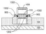
- FIG. 4Aillustrates gates 402 that are formed around the nanowires 110 , as described in further detail below, and capped with a polysilicon layer (capping layer) 404 .
- a hardmask layer 406such as, for example silicon nitride (Si 3 N 4 ) is deposited over the polysilicon layer 404 .
- the polysilicon layer 404 and the hardmask layer 406may be formed by depositing polysilicon material over the BOX layer 104 and the SOI portion 102 , depositing the hardmask material over the polysilicon material, and etching by RIE to form the polysilicon layer 406 and the hardmask layer 404 illustrated in FIG. 4A .
- the etching of the gate 402may be performed by directional etching that results in straight sidewalls of the gate 402 . Following the directional etching, polysilicon 404 remains under the nanowires 110 and outside the region encapsulated by the gate 402 . Isotropic etching may be performed to remove polysilicon 404 from under the nanowires 110 .
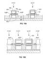
- FIG. 4Billustrates a perspective view of an exemplary alternate arrangement that includes a plurality of gates 402 that are formed on a nanowire 110 between SOI pad regions 106 and 108 .
- the fabrication of the arrangement shown in FIG. 4Bmay be performed using similar methods as described above for the fabrication of a single row of gates 402 line, and illustrates how the methods described herein may be used to form any number of devices on a nanowire between SOI pad regions 106 and 108 .
- FIG. 5illustrates a cross sectional view of a gate 402 along the line A-A (of FIG. 4A ).
- the gate 402is formed by depositing a first gate dielectric layer 502 , such as silicon dioxide (SiO 2 ) around a channel portion of the nanowire 110 .
- a second gate dielectric layer 504such as, for example, hafnium oxide (HfO 2 ) is formed around the first gate dielectric layer 502 .
- a metal layer 506such as, for example, tantalum nitride (TaN) is formed around the second gate dielectric layer 504 .
- the metal layer 506is surrounded by polysilicon layer 404 (of FIG. 4A ). Doping the polysilicon layer 404 with impurities such as boron (p-type), or phosphorus (n-type) makes the polysilicon layer 404 conductive.
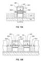
- FIGS. 6A and 6Billustrate the spacer portions 604 formed along opposing sides of the polysilicon layer 404 .
- the spacersare formed by depositing a blanket dielectric film such as silicon nitride and etching the dielectric film from all horizontal surfaces by RIE.
- the spacer walls 604are formed around portions of the nanowire 110 that extend from the polysilicon layer 404 and surround portions of the nanowires 110 .
- FIGS. 6A and 6Binclude spacer portions 602 that are formed under the nanowires 110 , and in the undercut regions 202 (of FIG. 2 ).
- FIG. 7Aillustrates a cross-sectional view (of FIG. 6A ).
- FIG. 7Billustrates a similar cross-sectional view of the exemplary alternate arrangement of FIG. 6B .
- FIGS. 8A and 8Billustrate cross-sectional views of the resultant structures following a selective RIE process, that removes exposed portions of the nanowires 110 and the SOI pad regions 106 and 108 (shown in FIG. 7A ).
- An example of a selective RIE processincludes a RIE based on HBr chemistry that etches silicon while being selective to reduce the etching of dielectrics such as silicon oxide and silicon nitride.
- the portions of the nanowire 110 that are surrounded by the spacer walls 604are not etched, and have exposed cross sections defined by the spacer walls 604 .
- FIGS. 9A and 9Billustrate cross-sectional views of the resultant structures following a selective epi-silicon growth to form epi-nanowire extensions 902 (nanowire extensions).
- the nanowire extensions 902are epitaxially grown from the exposed cross-sectional portions of the nanowire 110 that are surrounded by the spacer walls 604 .
- the nanowire extensions 902are formed by epitaxially growing, for example, in-situ doped silicon (Si) or a silicon germanium (SiGe) that may be either n-type or p-type doped.
- the in-situ doped epi processforms the source region and the drain region of the nanowire FET.
- a chemical vapor deposition (CVD) reactormay be used to perform the epitaxial growth.
- Precursors for silicon epitaxyinclude SiCl 4 , SiH 4 combined with HCL. The use of chlorine allows selective deposition of silicon only on exposed silicon surfaces.
- a precursor for SiGemay be GeH 4 , which may obtain deposition selectivity without HCL.
- Precursors for dopantsmay include PH 3 or AsH 3 for n-type doping and B 2 H 6 for p-type doping.
- Deposition temperaturesmay range from 550° C. to 1000° C. for pure silicon deposition, and as low as 300° C. for pure Ge deposition.
- FIGS. 10A-11Billustrate an exemplary method for fabricating complementary metal-oxide-semiconductors (CMOS) having both N-FETs and P-FETs fabricated on the same chip. Since N-FETs and P-FETs have nanowire extensions with different types of dopants, the N-FET device and P-FET device nanowire extensions are grown in separately.
- CMOScomplementary metal-oxide-semiconductors
- FIG. 10Billustrates a similar process as described in FIG. 10A for a plurality of N-FET and P-FET devices.
- the epi blocking masks 1001are removed, and a second epi blocking mask 1101 is deposited and patterned to cover the P-FET and the p+ doped nanowire extensions 902 P.
- Selective epitaxy with n-type in-situ dopingis used to form the n+ doped nanowire extensions 902 N.
- the second epi blocking mask 1101may be removed.
- the order by which the P-FET and N-FET nanowire extensions 902 are formedmay be chosen to minimize diffusion of dopants in the first grown extension during the growth of the second nanowire extension.
- the epitaxy of the n+ doped nanowire extensions 902 Nmay be formed prior to forming the p+ doped nanowire extensions 902 P. Since the formation of the nanowire extensions 902 may be carried out in separate processing steps, the extensions composition may be different. For example, SiGe nanowire extensions may be formed for the P-FET devices while pure silicon nanowire extensions may be formed for the N-FET devices.
- FIGS. 12A and 12Billustrate an example of the resultant structures following a thermal process (performed after the growth of the nanowire extensions 902 described above) that diffuses the doped ions from the nanowire extensions 902 into the regions 1202 of the nanowires 110 that are surrounded by the spacer walls 604 and the gates 404 to overlap the device.
- the epi-nanowire extensions 902are uniformly doped when grown; resulting in a uniform doping profile in the regions 1202 of the nanowires 110 following diffusion of the ions from the epi-nanowire extension 902 into the regions 1202 .
- CMOS devicesdescribed above in FIGS. 10A-11B
- a similar thermal processmay be performed.
- the thermal processmay be performed in a rapid thermal annealing (RTA) chamber.
- the thermal processmay be performed, for example, at annealing temperatures between 900° C. to 1100° C. for 0-10 seconds in an ambient N 2 gas.
- the annealing temperature ratemay range, for example, between 50° C./second to 300° C./second.
- FIGS. 13A and 13Billustrate a resultant structure following silicidation where a silicide 1302 is formed on the nanowire extensions 902 , and over the polysilicon layer 404 .
- silicide forming metalsinclude Ni, Pt, Co, and alloys such as NiPt. When Ni is used the NiSi phase is formed due to its low resistivity. For example, formation temperatures include 400-600° C.
- FIGS. 14A-15Billustrate an alternate exemplary method for forming a nanowire FET.
- the alternate exemplary methodis similar to the method described above in FIGS. 1-13B .
- the etching processremoves a portion of the nanowires 110 that are surrounded by the spacer walls 604 and the gates 402 to recess the nanowires 110 into the gates 402 , and form cavities 1402 defined by the gates 402 , the nanowires 110 and the spacer walls 604 .
- FIGS. 14A and 14Billustrate a cross-sectional view of the resultant structure.
- the lateral etching process that forms cavities 1402may be time based. Width variation in spacer 604 may lead to variations in the position of the edges of the recessed nanowires 110 .
- the etching rate in the cavity 1402depends on the size of the cavity, with narrower orifice corresponding to slower etch rates. Variations in the nanowire size will therefore lead to variations in the depth of cavity 1402 .
- the variations described abovemay be reduced by bombarding the exposed ends of nanowire 110 with ions (e.g. silicon ions, germanium ions, and even dopants such as boron which do not amorphize) prior to the formation of the spacer 604 (in FIGS. 6A and 6B ).
- ionse.g. silicon ions, germanium ions, and even dopants such as boron which do not amorphize
- the etching rate of the bombarded portions of nanowires 110is several times faster than that of the un-exposed portion of nanowire 110 protected by gate material 402 .
- the cavity 1402becomes self-aligned with the sidewalls of gate 402 when etched.
- the deposition processmay anneal the exposed nanowire 110 portions (that have been bombarded with ions) and increase the etching resistance of the exposed nanowire 110 portion.
- the spacer 604may be formed at a low temperature, for example, less than 500° C. to avoid annealing the bombarded portions of the nanowires 110 . If other materials are used to form the nanowires 110 are used, the formation temperature of the spacer 604 may be higher.
- An alternative that accommodates high temperature deposition of spacer 604includes performing an ion implantation at an oblique angle to the substrate 100 after the deposition of the spacer 604 with an ion energy that damages the portions of the nanowires 110 that are encapsulated by spacer 604 .
- FIGS. 15A and 15Ba cross-sectional view of the resultant structure having nanowire extensions 1502 that are formed from an in-situ doped epi-silicon growth process similar to the process described above in FIGS. 9A and 9B .
- the epi silicon growthbegan in the cavity 1402 (of FIGS. 14A and 14B ) from the exposed nanowire 110 in the gate 402 to form the nanowire extensions 1502 .
- the dopingmay be activated by, for example, a laser or flash anneal process.
- the laser or flash annealingmay reduce diffusion of ions into the channel region 1501 of the gate 402 , and result in a high uniform concentration of doping in the nanowire extensions 1502 with an abrupt junction in the nanowires 110 .
- silicidation similar to the process described in FIGS. 13A and 13B abovemay be performed and capping layers and vias for connectivity (not shown) may be formed.
Landscapes
- Engineering & Computer Science (AREA)
- Chemical & Material Sciences (AREA)
- Nanotechnology (AREA)
- Physics & Mathematics (AREA)
- Mathematical Physics (AREA)
- Theoretical Computer Science (AREA)
- Crystallography & Structural Chemistry (AREA)
- Thin Film Transistor (AREA)
Abstract
Description
- This application is related to co-pending application docket numbers YOR920090399US1, YOR920090411US1, YOR920090414US1, YOR920090505US1, YOR920090506US1, all of which are incorporated by reference herein.
- The present invention relates to semiconductor nanowire field effect transistors.
- A nanowire field effect transistor (FET) includes doped portions of nanowire that contact the channel region and serve as source and drain regions of the device. Previous fabrication methods that used ion-implantation to dope the small diameter nanowire may result in undesirable amorphization of the nanowire or an undesirable junction doping profile.
- In one aspect of the present invention, a method for forming a nanowire field effect transistor (FET) device, the method includes forming a suspended nanowire over a semiconductor substrate, forming a gate structure around a portion of the nanowire, forming a protective spacer adjacent to sidewalls of the gate and around portions of nanowire extending from the gate, removing exposed portions of the nanowire left unprotected by the spacer structure, and epitaxially growing a doped semiconductor material on exposed cross sections of the nanowire to form a source region and a drain region.
- In another aspect of the present invention, a method for forming a nanowire field effect transistor (FET) device, the method includes forming a suspended nanowire over a semiconductor substrate, forming a gate structure around a portion of the nanowire, forming a protective spacer adjacent to sidewalls of the gate and around portions of nanowire extending from the gate, removing exposed portions of the nanowire, and portions of nanowire to form a cavity defined by the nanowire surrounded by the gate structure, and the spacer walls, and epitaxially growing a doped semiconductor material in the cavity on exposed cross sections of the nanowire.
- In yet another aspect of the present invention, a nanowire field effect transistor (FET) device includes a channel region including a silicon portion having a first distal end extending from the channel region and a second distal end extending from the channel region, the silicon portion is partially surrounded by a gate structure disposed circumferentially around the silicon portion, a source region including a first doped epi-silicon nanowire extension contacting the first distal end of the silicon portion, and a drain region including a second doped epi-silicon nanowire extension contacting the second distal end of the silicon portion.
- In yet another aspect of the present invention, a nanowire field effect transistor (FET) device includes a channel region including a silicon portion having a first distal end and a second distal end, the silicon portion is surrounded by a gate structure disposed circumferentially around the silicon portion, a first cavity defined by the first distal end of the silicon portion and an inner diameter of the gate structure, a second cavity defined by the second distal end of the silicon portion and an inner diameter of the gate structure, a source region including a first doped epi-silicon nanowire extension contacting the first distal end of the silicon portion in the first cavity, and a drain region including a second doped epi-silicon nanowire extension contacting the second distal end of the silicon portion in the second cavity.
- Additional features and advantages are realized through the techniques of the present invention. Other embodiments and aspects of the invention are described in detail herein and are considered a part of the claimed invention. For a better understanding of the invention with the advantages and the features, refer to the description and to the drawings.
- The subject matter which is regarded as the invention is particularly pointed out and distinctly claimed in the claims at the conclusion of the specification. The forgoing and other features, and advantages of the invention are apparent from the following detailed description taken in conjunction with the accompanying drawings in which:
FIGS. 1-13B illustrate an exemplary method for forming field effect transistor (FET) devices.FIGS. 14A-15B illustrate an alternate exemplary method for forming field effect transistor (FET) devices.- With reference now to
FIG. 1 , a silicon on insulator (SOI)portion 102 is defined on a buried oxide (BOX)layer 104 that is disposed on asilicon substrate 100. TheSOI portion 102 includes aSOI pad region 106, aSOI pad region 108, and nanowireportions 109. TheSOI portion 102 may be patterned by the use of lithography followed by an etching process such as, for example, reactive ion etching (RIE). FIG. 2 illustrates theresultant BOX layer 104 andSOI portion 102 following an isotropic etching process. TheBOX layer 104 is recessed in regions not covered bySOI portion 102. The isotropic etching results in the lateral etching of portions of theBOX layer 104 that are under theSOI portion 102. The lateral etch suspends thenanowires 109 above theBOX layer 104. The lateral etch forms theundercuts 202 in theBOX layer 104 and overhangportions 201 at the edges ofSOI regions BOX layer 104 may be, for example, performed using a diluted hydrofluoric acid (DHF). A 100:1 DHF etches about 2 to 3 nm ofBOX layer 104 per minute at room temperature. Following the isotropic etching thenanowires portions 109 are smoothed to form elliptical shaped (and in some cases, cylindrical shaped)nanowires 110 that are suspended above theBOX layer 104 by theSOI pad region 106 and theSOI pad region 108. The smoothing of the nanowires may be performed by, for example, annealing of thenanowires 109 in hydrogen. Example annealing temperatures may be in the range of 600° C.-900° C., and a hydrogen pressure of approximately 600 torr to 7 torr.FIG. 3 illustrates thenanowires 110 following an oxidation process that reduces the diameter of thenanowires 110. The reduction of the diameter of thenanowires 110 may be performed by, for example, an oxidation of thenanowires 110 followed by the etching of the grown oxide. The oxidation and etching process may be repeated to achieve a desirednanowire 110 diameter. Once the diameters of thenanowires 110 have been reduced, gates are formed over the channel regions of the nanowires110 (described below).FIG. 4A illustratesgates 402 that are formed around thenanowires 110, as described in further detail below, and capped with a polysilicon layer (capping layer)404. Ahardmask layer 406, such as, for example silicon nitride (Si3N4) is deposited over thepolysilicon layer 404. Thepolysilicon layer 404 and thehardmask layer 406 may be formed by depositing polysilicon material over theBOX layer 104 and theSOI portion 102, depositing the hardmask material over the polysilicon material, and etching by RIE to form thepolysilicon layer 406 and thehardmask layer 404 illustrated inFIG. 4A . The etching of thegate 402 may be performed by directional etching that results in straight sidewalls of thegate 402. Following the directional etching,polysilicon 404 remains under thenanowires 110 and outside the region encapsulated by thegate 402. Isotropic etching may be performed to removepolysilicon 404 from under thenanowires 110.FIG. 4B illustrates a perspective view of an exemplary alternate arrangement that includes a plurality ofgates 402 that are formed on ananowire 110 betweenSOI pad regions FIG. 4B may be performed using similar methods as described above for the fabrication of a single row ofgates 402 line, and illustrates how the methods described herein may be used to form any number of devices on a nanowire betweenSOI pad regions FIG. 5 illustrates a cross sectional view of agate 402 along the line A-A (ofFIG. 4A ). Thegate 402 is formed by depositing a first gatedielectric layer 502, such as silicon dioxide (SiO2) around a channel portion of thenanowire 110. A second gatedielectric layer 504 such as, for example, hafnium oxide (HfO2) is formed around the first gatedielectric layer 502. Ametal layer 506 such as, for example, tantalum nitride (TaN) is formed around the second gatedielectric layer 504. Themetal layer 506 is surrounded by polysilicon layer404 (ofFIG. 4A ). Doping thepolysilicon layer 404 with impurities such as boron (p-type), or phosphorus (n-type) makes thepolysilicon layer 404 conductive.FIGS. 6A and 6B illustrate thespacer portions 604 formed along opposing sides of thepolysilicon layer 404. The spacers are formed by depositing a blanket dielectric film such as silicon nitride and etching the dielectric film from all horizontal surfaces by RIE. Thespacer walls 604 are formed around portions of thenanowire 110 that extend from thepolysilicon layer 404 and surround portions of thenanowires 110.FIGS. 6A and 6B includespacer portions 602 that are formed under thenanowires 110, and in the undercut regions202 (ofFIG. 2 ).FIG. 7A illustrates a cross-sectional view (ofFIG. 6A ).FIG. 7B illustrates a similar cross-sectional view of the exemplary alternate arrangement ofFIG. 6B .FIGS. 8A and 8B illustrate cross-sectional views of the resultant structures following a selective RIE process, that removes exposed portions of thenanowires 110 and theSOI pad regions 106 and108 (shown inFIG. 7A ). An example of a selective RIE process includes a RIE based on HBr chemistry that etches silicon while being selective to reduce the etching of dielectrics such as silicon oxide and silicon nitride. The portions of thenanowire 110 that are surrounded by thespacer walls 604 are not etched, and have exposed cross sections defined by thespacer walls 604.FIGS. 9A and 9B illustrate cross-sectional views of the resultant structures following a selective epi-silicon growth to form epi-nanowire extensions902 (nanowire extensions). Thenanowire extensions 902 are epitaxially grown from the exposed cross-sectional portions of thenanowire 110 that are surrounded by thespacer walls 604. Thenanowire extensions 902 are formed by epitaxially growing, for example, in-situ doped silicon (Si) or a silicon germanium (SiGe) that may be either n-type or p-type doped. The in-situ doped epi process forms the source region and the drain region of the nanowire FET. As an example, a chemical vapor deposition (CVD) reactor may be used to perform the epitaxial growth. Precursors for silicon epitaxy include SiCl4, SiH4combined with HCL. The use of chlorine allows selective deposition of silicon only on exposed silicon surfaces. A precursor for SiGe may be GeH4, which may obtain deposition selectivity without HCL. Precursors for dopants may include PH3or AsH3for n-type doping and B2H6for p-type doping. Deposition temperatures may range from 550° C. to 1000° C. for pure silicon deposition, and as low as 300° C. for pure Ge deposition.FIGS. 10A-11B illustrate an exemplary method for fabricating complementary metal-oxide-semiconductors (CMOS) having both N-FETs and P-FETs fabricated on the same chip. Since N-FETs and P-FETs have nanowire extensions with different types of dopants, the N-FET device and P-FET device nanowire extensions are grown in separately. Referring toFIG. 10A , a P-FET and N-FET device is shown. The N-FET is covered with anepi blocking mask 1001 that blocks the growth from the exposed cross-sectional portions of thenanowire 110. Theepi blocking mask 1001 may be, for example, a deposited oxide film that is patterned to cover the N-FET devices. The P-FET cross-sectional portions of thenanowire 110 are exposed allowing the formation of the p+ dopednanowire extensions 902P using a selective epitaxially grown silicon deposition process similar to the process described above.FIG. 10B illustrates a similar process as described inFIG. 10A for a plurality of N-FET and P-FET devices.- Referring to
FIGS. 11A and 11B , following the growth of the p+ dopednanowire extensions 902P (inFIGS. 10A and 10B ), theepi blocking masks 1001 are removed, and a secondepi blocking mask 1101 is deposited and patterned to cover the P-FET and the p+ dopednanowire extensions 902P. Selective epitaxy with n-type in-situ doping is used to form the n+ dopednanowire extensions 902N. Once the n+ dopednanowire extensions 902N are formed, the secondepi blocking mask 1101 may be removed. The order by which the P-FET and N-FET nanowire extensions 902 are formed may be chosen to minimize diffusion of dopants in the first grown extension during the growth of the second nanowire extension. Thus, the epitaxy of the n+ dopednanowire extensions 902N may be formed prior to forming the p+ dopednanowire extensions 902P. Since the formation of thenanowire extensions 902 may be carried out in separate processing steps, the extensions composition may be different. For example, SiGe nanowire extensions may be formed for the P-FET devices while pure silicon nanowire extensions may be formed for the N-FET devices. FIGS. 12A and 12B illustrate an example of the resultant structures following a thermal process (performed after the growth of thenanowire extensions 902 described above) that diffuses the doped ions from thenanowire extensions 902 into theregions 1202 of thenanowires 110 that are surrounded by thespacer walls 604 and thegates 404 to overlap the device. The epi-nanowire extensions 902 are uniformly doped when grown; resulting in a uniform doping profile in theregions 1202 of thenanowires 110 following diffusion of the ions from the epi-nanowire extension 902 into theregions 1202. For the CMOS devices (described above inFIGS. 10A-11B ), a similar thermal process may be performed. When the n-type and p-type dopant diffusion properties are similar, similar doped regions of thenanowires 110 for both PFET and NFET devices will result. When the n-type and p-type dopant diffusion properties are dissimilar, the penetration of the n-type and p-type dopants may result indissimilar regions 1202 in thenanowires 110. The thermal process may be performed in a rapid thermal annealing (RTA) chamber. The thermal process may be performed, for example, at annealing temperatures between 900° C. to 1100° C. for 0-10 seconds in an ambient N2gas. The annealing temperature rate may range, for example, between 50° C./second to 300° C./second.FIGS. 13A and 13B illustrate a resultant structure following silicidation where asilicide 1302 is formed on thenanowire extensions 902, and over thepolysilicon layer 404. Examples of silicide forming metals include Ni, Pt, Co, and alloys such as NiPt. When Ni is used the NiSi phase is formed due to its low resistivity. For example, formation temperatures include 400-600° C. Once the silicidation process is performed, capping layers and vias for connectivity (not shown) may be formed.FIGS. 14A-15B illustrate an alternate exemplary method for forming a nanowire FET. The alternate exemplary method is similar to the method described above inFIGS. 1-13B . However, when thenanowires 110 are etched to remove the exposed portions of thenanowires 110, the etching process removes a portion of thenanowires 110 that are surrounded by thespacer walls 604 and thegates 402 to recess thenanowires 110 into thegates 402, andform cavities 1402 defined by thegates 402, thenanowires 110 and thespacer walls 604.FIGS. 14A and 14B illustrate a cross-sectional view of the resultant structure.- The lateral etching process that forms
cavities 1402 may be time based. Width variation inspacer 604 may lead to variations in the position of the edges of the recessednanowires 110. The etching rate in thecavity 1402 depends on the size of the cavity, with narrower orifice corresponding to slower etch rates. Variations in the nanowire size will therefore lead to variations in the depth ofcavity 1402. - The variations described above may be reduced by bombarding the exposed ends of
nanowire 110 with ions (e.g. silicon ions, germanium ions, and even dopants such as boron which do not amorphize) prior to the formation of the spacer604 (inFIGS. 6A and 6B ). The etching rate of the bombarded portions ofnanowires 110 is several times faster than that of the un-exposed portion ofnanowire 110 protected bygate material 402. As a result, thecavity 1402 becomes self-aligned with the sidewalls ofgate 402 when etched. - If the deposition of
spacer 604 is performed at an elevated temperature, the deposition process may anneal the exposednanowire 110 portions (that have been bombarded with ions) and increase the etching resistance of the exposednanowire 110 portion. Forsilicon nanowires 110, thespacer 604 may be formed at a low temperature, for example, less than 500° C. to avoid annealing the bombarded portions of thenanowires 110. If other materials are used to form thenanowires 110 are used, the formation temperature of thespacer 604 may be higher. An alternative that accommodates high temperature deposition ofspacer 604 includes performing an ion implantation at an oblique angle to thesubstrate 100 after the deposition of thespacer 604 with an ion energy that damages the portions of thenanowires 110 that are encapsulated byspacer 604. - Referring to
FIGS. 15A and 15B , a cross-sectional view of the resultant structure havingnanowire extensions 1502 that are formed from an in-situ doped epi-silicon growth process similar to the process described above inFIGS. 9A and 9B . The epi silicon growth began in the cavity1402 (ofFIGS. 14A and 14B ) from the exposednanowire 110 in thegate 402 to form thenanowire extensions 1502. Oncenanowire extensions 1502 are formed, the doping may be activated by, for example, a laser or flash anneal process. The laser or flash annealing may reduce diffusion of ions into thechannel region 1501 of thegate 402, and result in a high uniform concentration of doping in thenanowire extensions 1502 with an abrupt junction in thenanowires 110. Once the ions have been activated, silicidation similar to the process described inFIGS. 13A and 13B above may be performed and capping layers and vias for connectivity (not shown) may be formed. - The terminology used herein is for the purpose of describing particular embodiments only and is not intended to be limiting of the invention. As used herein, the singular forms “a”, “an” and “the” are intended to include the plural forms as well, unless the context clearly indicates otherwise. It will be further understood that the terms “comprises” and/or “comprising,” when used in this specification, specify the presence of stated features, integers, steps, operations, elements, and/or components, but do not preclude the presence or addition of one or more other features, integers, steps, operations, element components, and/or groups thereof.
- The corresponding structures, materials, acts, and equivalents of all means or step plus function elements in the claims below are intended to include any structure, material, or act for performing the function in combination with other claimed elements as specifically claimed. The description of the present invention has been presented for purposes of illustration and description, but is not intended to be exhaustive or limited to the invention in the form disclosed. Many modifications and variations will be apparent to those of ordinary skill in the art without departing from the scope and spirit of the invention. The embodiment was chosen and described in order to best explain the principles of the invention and the practical application, and to enable others of ordinary skill in the art to understand the invention for various embodiments with various modifications as are suited to the particular use contemplated
- The diagrams depicted herein are just one example. There may be many variations to this diagram or the steps (or operations) described therein without departing from the spirit of the invention. For instance, the steps may be performed in a differing order or steps may be added, deleted or modified. All of these variations are considered a part of the claimed invention.
- While the preferred embodiment to the invention had been described, it will be understood that those skilled in the art, both now and in the future, may make various improvements and enhancements which fall within the scope of the claims which follow. These claims should be construed to maintain the proper protection for the invention first described.
Claims (35)
Priority Applications (3)
| Application Number | Priority Date | Filing Date | Title |
|---|---|---|---|
| US12/631,199US8384065B2 (en) | 2009-12-04 | 2009-12-04 | Gate-all-around nanowire field effect transistors |
| PCT/EP2010/066483WO2011067050A1 (en) | 2009-12-04 | 2010-10-29 | Gate-all-around nanowire field effect transistors |
| CN201080054985.6ACN102640271B (en) | 2009-12-04 | 2010-10-29 | Gate-all-around nanowire field effect transistors |
Applications Claiming Priority (1)
| Application Number | Priority Date | Filing Date | Title |
|---|---|---|---|
| US12/631,199US8384065B2 (en) | 2009-12-04 | 2009-12-04 | Gate-all-around nanowire field effect transistors |
Publications (2)
| Publication Number | Publication Date |
|---|---|
| US20110133162A1true US20110133162A1 (en) | 2011-06-09 |
| US8384065B2 US8384065B2 (en) | 2013-02-26 |
Family
ID=43216723
Family Applications (1)
| Application Number | Title | Priority Date | Filing Date |
|---|---|---|---|
| US12/631,199Active2031-06-15US8384065B2 (en) | 2009-12-04 | 2009-12-04 | Gate-all-around nanowire field effect transistors |
Country Status (3)
| Country | Link |
|---|---|
| US (1) | US8384065B2 (en) |
| CN (1) | CN102640271B (en) |
| WO (1) | WO2011067050A1 (en) |
Cited By (30)
| Publication number | Priority date | Publication date | Assignee | Title |
|---|---|---|---|---|
| US20120299100A1 (en)* | 2011-05-27 | 2012-11-29 | Kensuke Ota | Semiconductor device and method of manufacturing the same |
| WO2013070394A1 (en)* | 2011-11-09 | 2013-05-16 | International Business Machines Corporation | Nanowire field effect transistor device |
| US20130187129A1 (en)* | 2010-06-21 | 2013-07-25 | International Business Machines Corporation | Semiconductor devices fabricated by doped material layer as dopant source |
| US8507892B2 (en)* | 2009-12-04 | 2013-08-13 | International Business Machines Corporation | Omega shaped nanowire tunnel field effect transistors |
| CN103258741A (en)* | 2012-02-20 | 2013-08-21 | 中芯国际集成电路制造(上海)有限公司 | Nanowire field effect transistor and forming method thereof |
| CN103258738A (en)* | 2012-02-20 | 2013-08-21 | 中芯国际集成电路制造(上海)有限公司 | Superlattice nanowire field effect transistor and forming method thereof |
| US8536029B1 (en) | 2012-06-21 | 2013-09-17 | International Business Machines Corporation | Nanowire FET and finFET |
| US8541295B2 (en) | 2012-02-27 | 2013-09-24 | International Business Machines Corporation | Pad-less gate-all around semiconductor nanowire FETs on bulk semiconductor wafers |
| US8679902B1 (en) | 2012-09-27 | 2014-03-25 | International Business Machines Corporation | Stacked nanowire field effect transistor |
| US8686485B2 (en) | 2012-03-20 | 2014-04-01 | Samsung Electronics Co., Ltd. | Semiconductor devices and methods of manufacturing the same |
| US20140138771A1 (en)* | 2012-11-16 | 2014-05-22 | International Business Machines Corporation | Local tailoring of fingers in multi-finger fin field effect transistors |
| US20140151705A1 (en)* | 2012-12-04 | 2014-06-05 | Semiconductor Manufacturing International Corp. | Nanowires, nanowire fielde-effect transistors and fabrication method |
| CN103915335A (en)* | 2013-01-08 | 2014-07-09 | 中芯国际集成电路制造(上海)有限公司 | Forming method of semiconductor device |
| WO2014116433A1 (en)* | 2013-01-24 | 2014-07-31 | Intel Corporation | Deep gate-all-around semiconductor device having germanium or group iii-v active layer |
| US8802512B2 (en)* | 2013-01-11 | 2014-08-12 | International Business Machines Corporation | Overlap capacitance nanowire |
| US8816327B2 (en) | 2011-11-01 | 2014-08-26 | International Business Machines Corporation | Nanowire efuses |
| US20140332753A1 (en)* | 2013-05-09 | 2014-11-13 | Semiconductor Manufacturing International (Shanghai) Corporation | Nano field-effect vacuum tube and fabrication method thereof |
| US8901655B2 (en) | 2013-02-07 | 2014-12-02 | International Business Machines Corporation | Diode structure for gate all around silicon nanowire technologies |
| US8928083B2 (en) | 2013-02-07 | 2015-01-06 | International Business Machines Corporation | Diode structure and method for FINFET technologies |
| JP2015508575A (en)* | 2012-01-05 | 2015-03-19 | インターナショナル・ビジネス・マシーンズ・コーポレーションInternational Business Machines Corporation | Field effect transistor and method for forming the same |
| US8994108B2 (en) | 2013-02-07 | 2015-03-31 | International Business Machines Corporation | Diode structure and method for wire-last nanomesh technologies |
| US20150140762A1 (en)* | 2012-12-13 | 2015-05-21 | International Business Machines Corporation | Finfet with merge-free fins |
| CN104979211A (en)* | 2014-04-10 | 2015-10-14 | 中芯国际集成电路制造(上海)有限公司 | Nano wire device and manufacturing method thereof |
| US9287360B1 (en)* | 2015-01-07 | 2016-03-15 | International Business Machines Corporation | III-V nanowire FET with compositionally-graded channel and wide-bandgap core |
| US20160190210A1 (en)* | 2014-12-29 | 2016-06-30 | Semiconductor Manufacturing International (Shanghai) Corporation | Complementary carbon nanotube neuron device |
| US9502518B2 (en)* | 2014-06-23 | 2016-11-22 | Stmicroelectronics, Inc. | Multi-channel gate-all-around FET |
| US10043665B2 (en)* | 2016-11-28 | 2018-08-07 | Taiwan Semiconductor Manufacturing Co., Ltd. | Formation method of semiconductor device structure with semiconductor nanowire |
| EP3502049A1 (en)* | 2017-12-22 | 2019-06-26 | Commissariat à l'énergie atomique et aux énergies alternatives | Method for manufacturing a semiconductor device comprising one or more nanostructures |
| US10651291B2 (en) | 2017-08-18 | 2020-05-12 | Globalfoundries Inc. | Inner spacer formation in a nanosheet field-effect transistor |
| US10755937B2 (en)* | 2017-04-07 | 2020-08-25 | Semiconductor Manufacturing International (Shanghai) Corporation | Vertical transistor having a silicided bottom and method for fabricating thereof |
Families Citing this family (21)
| Publication number | Priority date | Publication date | Assignee | Title |
|---|---|---|---|---|
| US8890264B2 (en)* | 2012-09-26 | 2014-11-18 | Intel Corporation | Non-planar III-V field effect transistors with conformal metal gate electrode and nitrogen doping of gate dielectric interface |
| US9257545B2 (en) | 2013-09-12 | 2016-02-09 | Globalfoundries Inc. | Stacked nanowire device with variable number of nanowire channels |
| US9263520B2 (en) | 2013-10-10 | 2016-02-16 | Globalfoundries Inc. | Facilitating fabricating gate-all-around nanowire field-effect transistors |
| CN103700660A (en)* | 2013-12-11 | 2014-04-02 | 中国科学院上海微系统与信息技术研究所 | Whole annular grid CMOS (complementary metal oxide semiconductor) field effect transistor and preparing method |
| US9257527B2 (en) | 2014-02-14 | 2016-02-09 | International Business Machines Corporation | Nanowire transistor structures with merged source/drain regions using auxiliary pillars |
| US10396152B2 (en) | 2014-07-25 | 2019-08-27 | International Business Machines Corporation | Fabrication of perfectly symmetric gate-all-around FET on suspended nanowire using interface interaction |
| US9853166B2 (en) | 2014-07-25 | 2017-12-26 | International Business Machines Corporation | Perfectly symmetric gate-all-around FET on suspended nanowire |
| US9576856B2 (en) | 2014-10-27 | 2017-02-21 | Globalfoundries Inc. | Fabrication of nanowire field effect transistor structures |
| CN105810730B (en)* | 2014-12-29 | 2018-12-07 | 中芯国际集成电路制造(上海)有限公司 | Semiconductor device and its manufacturing method |
| US9362354B1 (en) | 2015-02-18 | 2016-06-07 | International Business Machines Corporation | Tuning gate lengths in semiconductor device structures |
| US9443949B1 (en) | 2015-03-27 | 2016-09-13 | International Business Machines Corporation | Techniques for multiple gate workfunctions for a nanowire CMOS technology |
| US9613871B2 (en) | 2015-07-16 | 2017-04-04 | Samsung Electronics Co., Ltd. | Semiconductor device and fabricating method thereof |
| US9607900B1 (en) | 2015-09-10 | 2017-03-28 | International Business Machines Corporation | Method and structure to fabricate closely packed hybrid nanowires at scaled pitch |
| CN116825818A (en)* | 2015-11-12 | 2023-09-29 | 蓝枪半导体有限责任公司 | Grid full-cladding nanowire field effect transistor device |
| CN106960793A (en)* | 2016-01-11 | 2017-07-18 | 中芯国际集成电路制造(上海)有限公司 | The forming method of fin and the forming method of fin field effect pipe |
| KR102527382B1 (en) | 2016-06-21 | 2023-04-28 | 삼성전자주식회사 | Semiconductor devices |
| US10103241B2 (en) | 2017-03-07 | 2018-10-16 | Nxp Usa, Inc. | Multigate transistor |
| US10186510B2 (en)* | 2017-05-01 | 2019-01-22 | Advanced Micro Devices, Inc. | Vertical gate all around library architecture |
| US10170304B1 (en) | 2017-10-25 | 2019-01-01 | Globalfoundries Inc. | Self-aligned nanotube structures |
| US10236346B1 (en) | 2017-10-25 | 2019-03-19 | International Business Machines Corporation | Transistor having a high germanium percentage fin channel and a gradient source/drain junction doping profile |
| US10714392B2 (en) | 2018-07-18 | 2020-07-14 | International Business Machines Corporation | Optimizing junctions of gate all around structures with channel pull back |
Citations (77)
| Publication number | Priority date | Publication date | Assignee | Title |
|---|---|---|---|---|
| US4995001A (en)* | 1988-10-31 | 1991-02-19 | International Business Machines Corporation | Memory cell and read circuit |
| US5308445A (en)* | 1991-10-23 | 1994-05-03 | Rohm Co., Ltd. | Method of manufacturing a semiconductor device having a semiconductor growth layer completely insulated from a substrate |
| US5438018A (en)* | 1992-12-07 | 1995-08-01 | Fujitsu Limited | Method of making semiconductor device by selective epitaxial growth |
| US5552622A (en)* | 1992-07-14 | 1996-09-03 | Mitsuteru Kimura | Tunnel transistor |
| US5668046A (en)* | 1991-03-27 | 1997-09-16 | Nec Corporation | Method of producing a semiconductor on insulating substrate, and a method of forming transistor thereon |
| US6365465B1 (en)* | 1999-03-19 | 2002-04-02 | International Business Machines Corporation | Self-aligned double-gate MOSFET by selective epitaxy and silicon wafer bonding techniques |
| US6642115B1 (en)* | 2000-05-15 | 2003-11-04 | International Business Machines Corporation | Double-gate FET with planarized surfaces and self-aligned silicides |
| US6653209B1 (en)* | 1999-09-30 | 2003-11-25 | Canon Kabushiki Kaisha | Method of producing silicon thin film, method of constructing SOI substrate and semiconductor device |
| US20040149978A1 (en)* | 2003-01-31 | 2004-08-05 | Greg Snider | Molecular-junction-nanowire-crossbar-based inverter, latch, and flip-flop circuits, and more complex circuits composed, in part, from molecular-junction-nanowire-crossbar-based inverter, latch, and flip-flop circuits |
| US20040166642A1 (en)* | 2003-02-20 | 2004-08-26 | Hao-Yu Chen | Semiconductor nano-rod devices |
| US6806141B2 (en)* | 2002-05-22 | 2004-10-19 | Hewlett-Packard Development Company, L.P. | Field effect transistor with gate layer and method of making same |
| US6835618B1 (en)* | 2003-08-05 | 2004-12-28 | Advanced Micro Devices, Inc. | Epitaxially grown fin for FinFET |
| US6882051B2 (en)* | 2001-03-30 | 2005-04-19 | The Regents Of The University Of California | Nanowires, nanostructures and devices fabricated therefrom |
| US6891227B2 (en)* | 2002-03-20 | 2005-05-10 | International Business Machines Corporation | Self-aligned nanotube field effect transistor and method of fabricating same |
| US6903013B2 (en)* | 2003-05-16 | 2005-06-07 | Chartered Semiconductor Manufacturing Ltd. | Method to fill a trench and tunnel by using ALD seed layer and electroless plating |
| US20050266645A1 (en)* | 2004-05-25 | 2005-12-01 | Jin-Jun Park | Phosphorous doping methods of manufacturing field effect transistors having multiple stacked channels |
| US20050275010A1 (en)* | 2004-06-10 | 2005-12-15 | Hung-Wei Chen | Semiconductor nano-wire devices and methods of fabrication |
| US20060033145A1 (en)* | 2004-08-13 | 2006-02-16 | Ronald Kakoschke | Integrated memory device and process |
| US20060138552A1 (en)* | 2004-09-30 | 2006-06-29 | Brask Justin K | Nonplanar transistors with metal gate electrodes |
| US7101762B2 (en)* | 2000-07-07 | 2006-09-05 | International Business Machines Corporation | Self-aligned double gate mosfet with separate gates |
| US7151209B2 (en)* | 2002-04-02 | 2006-12-19 | Nanosys, Inc. | Methods of making, positioning and orienting nanostructures, nanostructure arrays and nanostructure devices |
| US20070001219A1 (en)* | 2005-06-30 | 2007-01-04 | Marko Radosavljevic | Block contact architectures for nanoscale channel transistors |
| US7180107B2 (en)* | 2004-05-25 | 2007-02-20 | International Business Machines Corporation | Method of fabricating a tunneling nanotube field effect transistor |
| US7211853B2 (en)* | 2001-07-26 | 2007-05-01 | Technische Universiteit Delft | Electronic device using carbon nanotubes |
| US7253060B2 (en)* | 2004-06-08 | 2007-08-07 | Samsung Electronics Co., Ltd. | Gate-all-around type of semiconductor device and method of fabricating the same |
| US7297615B2 (en)* | 2005-05-13 | 2007-11-20 | Samsung Electronics, Co., Ltd. | Si nanowire substrate, method of manufacturing the same, and method of manufacturing thin film transistor using the same |
| US20070267619A1 (en)* | 2006-05-22 | 2007-11-22 | Thomas Nirschl | Memory using tunneling field effect transistors |
| US20070267703A1 (en)* | 2006-05-17 | 2007-11-22 | Chartered Semiconductor Manufacturing Ltd. | Strained channel transistor and method of fabrication thereof |
| US20070284613A1 (en)* | 2006-06-09 | 2007-12-13 | Chi On Chui | Strain-inducing semiconductor regions |
| US7311776B2 (en)* | 2003-12-30 | 2007-12-25 | The Regents Of The University Of California | Localized synthesis and self-assembly of nanostructures |
| US20080014689A1 (en)* | 2006-07-07 | 2008-01-17 | Texas Instruments Incorporated | Method for making planar nanowire surround gate mosfet |
| US20080061284A1 (en)* | 2006-09-11 | 2008-03-13 | International Business Machines Corporation | Nanowire MOSFET with doped epitaxial contacts for source and drain |
| US20080067495A1 (en)* | 2006-09-15 | 2008-03-20 | Interuniversitair Microelektronica Centrum (Imec) | Tunnel effect transistors based on silicon nanowires |
| US20080067607A1 (en)* | 2006-09-15 | 2008-03-20 | Interuniversitair Microelektronica Centrum (Imec) | Tunnel effect transistors based on elongate monocrystalline nanostructures having a heterostructure |
| US20080079041A1 (en)* | 2006-10-02 | 2008-04-03 | Samsung Electronics Co, Ltd. | Gate-all-around type semiconductor device and method of manufacturing the same |
| US20080085587A1 (en)* | 2006-10-04 | 2008-04-10 | Micron Technology, Inc. | Epitaxial silicon growth |
| US20080121932A1 (en)* | 2006-09-18 | 2008-05-29 | Pushkar Ranade | Active regions with compatible dielectric layers |
| US20080135949A1 (en)* | 2006-12-08 | 2008-06-12 | Agency For Science, Technology And Research | Stacked silicon-germanium nanowire structure and method of forming the same |
| US20080142853A1 (en)* | 2005-08-08 | 2008-06-19 | Freescale Semiconductor, Inc. | Multi-channel transistor structure and method of making thereof |
| US20080150025A1 (en)* | 2005-12-13 | 2008-06-26 | Versatilis Llc | Methods of Making Semiconductor-Based Electronic Devices on a Wire and by Forming Freestanding Semiconductor Structures, and Devices That Can Be Made Thereby |
| US20080149997A1 (en)* | 2006-12-20 | 2008-06-26 | Samsung Electronics Co., Ltd. | Nonvolatile memory device and method of operating the same |
| US20080149914A1 (en)* | 2006-12-22 | 2008-06-26 | Qunano Ab | Nanoelectronic structure and method of producing such |
| US20080179752A1 (en)* | 2007-01-26 | 2008-07-31 | Takashi Yamauchi | Method of making semiconductor device and semiconductor device |
| US20080191196A1 (en)* | 2005-06-06 | 2008-08-14 | Wei Lu | Nanowire heterostructures |
| US20080224224A1 (en)* | 2007-03-12 | 2008-09-18 | Interuniversitair Microelektronica Centrum Vzw (Imec) | Tunnel field-effect transistor with gated tunnel barrier |
| US20080227259A1 (en)* | 2005-01-07 | 2008-09-18 | International Business Machines Corporation | SELF-ALIGNED PROCESS FOR NANOTUBE/NANOWIRE FETs |
| US20080247226A1 (en)* | 2007-04-05 | 2008-10-09 | Micron Technology, Inc. | Memory devices having electrodes comprising nanowires, systems including same and methods of forming same |
| US20080246021A1 (en)* | 2006-10-04 | 2008-10-09 | Samsung Electronic Co., Ltd., | Single electron transistor and method of manufacturing the same |
| US7443025B2 (en)* | 2004-06-07 | 2008-10-28 | Broadcom Corporation | Thermally improved placement of power-dissipating components onto a circuit board |
| US7446025B2 (en)* | 2005-05-23 | 2008-11-04 | International Business Machines Corporation | Method of forming vertical FET with nanowire channels and a silicided bottom contact |
| US7449373B2 (en)* | 2006-03-31 | 2008-11-11 | Intel Corporation | Method of ion implanting for tri-gate devices |
| US7452759B2 (en)* | 2005-11-29 | 2008-11-18 | Micron Technology, Inc. | Carbon nanotube field effect transistor and methods for making same |
| US7456068B2 (en)* | 2006-06-08 | 2008-11-25 | Intel Corporation | Forming ultra-shallow junctions |
| US7456476B2 (en)* | 2003-06-27 | 2008-11-25 | Intel Corporation | Nonplanar semiconductor device with partially or fully wrapped around gate electrode and methods of fabrication |
| US7473943B2 (en)* | 2004-10-15 | 2009-01-06 | Nanosys, Inc. | Gate configuration for nanowire electronic devices |
| US20090026553A1 (en)* | 2007-07-25 | 2009-01-29 | Krishna Kumar Bhuwalka | Tunnel Field-Effect Transistor with Narrow Band-Gap Channel and Strong Gate Coupling |
| US7498211B2 (en)* | 2005-12-28 | 2009-03-03 | Intel Corporation | Independently controlled, double gate nanowire memory cell with self-aligned contacts |
| US20090061568A1 (en)* | 2007-09-05 | 2009-03-05 | International Business Machines Corporation | Techniques for Fabricating Nanowire Field-Effect Transistors |
| US20090057650A1 (en)* | 2000-08-22 | 2009-03-05 | President And Fellows Of Harvard College | Nanoscale wires and related devices |
| US20090057762A1 (en)* | 2007-09-05 | 2009-03-05 | International Business Machines Corporation | Nanowire Field-Effect Transistors |
| US20090090934A1 (en)* | 2007-10-05 | 2009-04-09 | Tsutomu Tezuka | Field Effect Transistor and Method for Manufacturing the Same |
| US20090134467A1 (en)* | 2007-11-26 | 2009-05-28 | Renesas Technology Corp. | Semiconductor device and a method of manufacturing the same |
| US7550333B2 (en)* | 2004-10-25 | 2009-06-23 | Intel Corporation | Nonplanar device with thinned lower body portion and method of fabrication |
| US20090181477A1 (en)* | 2005-07-01 | 2009-07-16 | Synopsys, Inc. | Integrated Circuit On Corrugated Substrate |
| US20090217216A1 (en)* | 2007-02-28 | 2009-08-27 | Motorola, Inc. | Carbon nanotube circuits design methodology |
| US20090290418A1 (en)* | 2008-05-20 | 2009-11-26 | Jung Chul Han | Method of verifying a program operation in a non-volatile memory device |
| US20090294864A1 (en)* | 2005-06-13 | 2009-12-03 | Samsung Electronics Co., Ltd. | Mos field effect transistor having plurality of channels |
| US7642578B2 (en)* | 2005-03-24 | 2010-01-05 | Samsung Electronics Co., Ltd. | Semiconductor device having a round-shaped nano-wire transistor channel and method of manufacturing same |
| US20100193770A1 (en)* | 2009-02-04 | 2010-08-05 | International Business Machines Corporation | Maskless Process for Suspending and Thinning Nanowires |
| US20100207102A1 (en)* | 2009-02-18 | 2010-08-19 | Samsung Electronics Co., Ltd. | Static random access memories having carbon nanotube thin films |
| US7791144B2 (en)* | 2006-04-28 | 2010-09-07 | International Business Machines Corporation | High performance stress-enhance MOSFET and method of manufacture |
| US7799657B2 (en)* | 2005-06-07 | 2010-09-21 | Freescale Semiconductor, Inc. | Method of fabricating a substrate for a planar, double-gated, transistor process |
| US7834345B2 (en)* | 2008-09-05 | 2010-11-16 | Taiwan Semiconductor Manufacturing Company, Ltd. | Tunnel field-effect transistors with superlattice channels |
| US7893506B2 (en)* | 2005-02-23 | 2011-02-22 | Intel Corporation | Field effect transistor with narrow bandgap source and drain regions and method of fabrication |
| US20110133169A1 (en)* | 2009-12-04 | 2011-06-09 | International Business Machines Corporation | Gate-All-Around Nanowire Tunnel Field Effect Transistors |
| US20110147840A1 (en)* | 2009-12-23 | 2011-06-23 | Cea Stephen M | Wrap-around contacts for finfet and tri-gate devices |
| US8097515B2 (en)* | 2009-12-04 | 2012-01-17 | International Business Machines Corporation | Self-aligned contacts for nanowire field effect transistors |
Family Cites Families (5)
| Publication number | Priority date | Publication date | Assignee | Title |
|---|---|---|---|---|
| US4638769A (en) | 1985-03-18 | 1987-01-27 | Caterpillar Inc. | Engine having a multipiece cylinder block |
| US6011081A (en)* | 1995-04-14 | 2000-01-04 | Benz Research And Development Corp. | Contact lens having improved dimensional stability |
| DE10118405A1 (en) | 2001-04-12 | 2002-10-24 | Infineon Technologies Ag | Heterostructure component used in electronic devices comprises a single hetero-nanotube having regions made from nanotube materials having different energy band gaps value |
| US7871851B2 (en) | 2007-05-25 | 2011-01-18 | RF Nano | Method for integrating nanotube devices with CMOS for RF/analog SoC applications |
| KR20090044799A (en) | 2007-11-01 | 2009-05-07 | 삼성전자주식회사 | Method for manufacturing active fin and transistor comprising same |
- 2009
- 2009-12-04USUS12/631,199patent/US8384065B2/enactiveActive
- 2010
- 2010-10-29WOPCT/EP2010/066483patent/WO2011067050A1/enactiveApplication Filing
- 2010-10-29CNCN201080054985.6Apatent/CN102640271B/enactiveActive
Patent Citations (88)
| Publication number | Priority date | Publication date | Assignee | Title |
|---|---|---|---|---|
| US4995001A (en)* | 1988-10-31 | 1991-02-19 | International Business Machines Corporation | Memory cell and read circuit |
| US5668046A (en)* | 1991-03-27 | 1997-09-16 | Nec Corporation | Method of producing a semiconductor on insulating substrate, and a method of forming transistor thereon |
| US5308445A (en)* | 1991-10-23 | 1994-05-03 | Rohm Co., Ltd. | Method of manufacturing a semiconductor device having a semiconductor growth layer completely insulated from a substrate |
| US5552622A (en)* | 1992-07-14 | 1996-09-03 | Mitsuteru Kimura | Tunnel transistor |
| US5438018A (en)* | 1992-12-07 | 1995-08-01 | Fujitsu Limited | Method of making semiconductor device by selective epitaxial growth |
| US5574308A (en)* | 1992-12-07 | 1996-11-12 | Fujitsu Limited | Semiconductor device and its manufacturing method |
| US6365465B1 (en)* | 1999-03-19 | 2002-04-02 | International Business Machines Corporation | Self-aligned double-gate MOSFET by selective epitaxy and silicon wafer bonding techniques |
| US6653209B1 (en)* | 1999-09-30 | 2003-11-25 | Canon Kabushiki Kaisha | Method of producing silicon thin film, method of constructing SOI substrate and semiconductor device |
| US6642115B1 (en)* | 2000-05-15 | 2003-11-04 | International Business Machines Corporation | Double-gate FET with planarized surfaces and self-aligned silicides |
| US7101762B2 (en)* | 2000-07-07 | 2006-09-05 | International Business Machines Corporation | Self-aligned double gate mosfet with separate gates |
| US20090057650A1 (en)* | 2000-08-22 | 2009-03-05 | President And Fellows Of Harvard College | Nanoscale wires and related devices |
| US6882051B2 (en)* | 2001-03-30 | 2005-04-19 | The Regents Of The University Of California | Nanowires, nanostructures and devices fabricated therefrom |
| US6996147B2 (en)* | 2001-03-30 | 2006-02-07 | The Regents Of The University Of California | Methods of fabricating nanostructures and nanowires and devices fabricated therefrom |
| US7569941B2 (en)* | 2001-03-30 | 2009-08-04 | The Regents Of The University Of California | Methods of fabricating nanostructures and nanowires and devices fabricated therefrom |
| US7211853B2 (en)* | 2001-07-26 | 2007-05-01 | Technische Universiteit Delft | Electronic device using carbon nanotubes |
| US6891227B2 (en)* | 2002-03-20 | 2005-05-10 | International Business Machines Corporation | Self-aligned nanotube field effect transistor and method of fabricating same |
| US7151209B2 (en)* | 2002-04-02 | 2006-12-19 | Nanosys, Inc. | Methods of making, positioning and orienting nanostructures, nanostructure arrays and nanostructure devices |
| US6806141B2 (en)* | 2002-05-22 | 2004-10-19 | Hewlett-Packard Development Company, L.P. | Field effect transistor with gate layer and method of making same |
| US20040149978A1 (en)* | 2003-01-31 | 2004-08-05 | Greg Snider | Molecular-junction-nanowire-crossbar-based inverter, latch, and flip-flop circuits, and more complex circuits composed, in part, from molecular-junction-nanowire-crossbar-based inverter, latch, and flip-flop circuits |
| US20050121706A1 (en)* | 2003-02-20 | 2005-06-09 | Hao-Yu Chen | Semiconductor nano-rod devices |
| US6855606B2 (en)* | 2003-02-20 | 2005-02-15 | Taiwan Semiconductor Manufacturing Company, Ltd. | Semiconductor nano-rod devices |
| US20040166642A1 (en)* | 2003-02-20 | 2004-08-26 | Hao-Yu Chen | Semiconductor nano-rod devices |
| US6903013B2 (en)* | 2003-05-16 | 2005-06-07 | Chartered Semiconductor Manufacturing Ltd. | Method to fill a trench and tunnel by using ALD seed layer and electroless plating |
| US7456476B2 (en)* | 2003-06-27 | 2008-11-25 | Intel Corporation | Nonplanar semiconductor device with partially or fully wrapped around gate electrode and methods of fabrication |
| US6835618B1 (en)* | 2003-08-05 | 2004-12-28 | Advanced Micro Devices, Inc. | Epitaxially grown fin for FinFET |
| US7311776B2 (en)* | 2003-12-30 | 2007-12-25 | The Regents Of The University Of California | Localized synthesis and self-assembly of nanostructures |
| US7180107B2 (en)* | 2004-05-25 | 2007-02-20 | International Business Machines Corporation | Method of fabricating a tunneling nanotube field effect transistor |
| US20050266645A1 (en)* | 2004-05-25 | 2005-12-01 | Jin-Jun Park | Phosphorous doping methods of manufacturing field effect transistors having multiple stacked channels |
| US7443025B2 (en)* | 2004-06-07 | 2008-10-28 | Broadcom Corporation | Thermally improved placement of power-dissipating components onto a circuit board |
| US7253060B2 (en)* | 2004-06-08 | 2007-08-07 | Samsung Electronics Co., Ltd. | Gate-all-around type of semiconductor device and method of fabricating the same |
| US20050275010A1 (en)* | 2004-06-10 | 2005-12-15 | Hung-Wei Chen | Semiconductor nano-wire devices and methods of fabrication |
| US7452778B2 (en)* | 2004-06-10 | 2008-11-18 | Taiwan Semiconductor Manufacturing Company, Ltd. | Semiconductor nano-wire devices and methods of fabrication |
| US20060033145A1 (en)* | 2004-08-13 | 2006-02-16 | Ronald Kakoschke | Integrated memory device and process |
| US20060138552A1 (en)* | 2004-09-30 | 2006-06-29 | Brask Justin K | Nonplanar transistors with metal gate electrodes |
| US20090149012A1 (en)* | 2004-09-30 | 2009-06-11 | Brask Justin K | Method of forming a nonplanar transistor with sidewall spacers |
| US7473943B2 (en)* | 2004-10-15 | 2009-01-06 | Nanosys, Inc. | Gate configuration for nanowire electronic devices |
| US7871870B2 (en)* | 2004-10-15 | 2011-01-18 | Nanosys, Inc. | Method of fabricating gate configurations for an improved contacts in nanowire based electronic devices |
| US7550333B2 (en)* | 2004-10-25 | 2009-06-23 | Intel Corporation | Nonplanar device with thinned lower body portion and method of fabrication |
| US20080227259A1 (en)* | 2005-01-07 | 2008-09-18 | International Business Machines Corporation | SELF-ALIGNED PROCESS FOR NANOTUBE/NANOWIRE FETs |
| US7893506B2 (en)* | 2005-02-23 | 2011-02-22 | Intel Corporation | Field effect transistor with narrow bandgap source and drain regions and method of fabrication |
| US7642578B2 (en)* | 2005-03-24 | 2010-01-05 | Samsung Electronics Co., Ltd. | Semiconductor device having a round-shaped nano-wire transistor channel and method of manufacturing same |
| US7297615B2 (en)* | 2005-05-13 | 2007-11-20 | Samsung Electronics, Co., Ltd. | Si nanowire substrate, method of manufacturing the same, and method of manufacturing thin film transistor using the same |
| US7446025B2 (en)* | 2005-05-23 | 2008-11-04 | International Business Machines Corporation | Method of forming vertical FET with nanowire channels and a silicided bottom contact |
| US20080191196A1 (en)* | 2005-06-06 | 2008-08-14 | Wei Lu | Nanowire heterostructures |
| US7799657B2 (en)* | 2005-06-07 | 2010-09-21 | Freescale Semiconductor, Inc. | Method of fabricating a substrate for a planar, double-gated, transistor process |
| US20090294864A1 (en)* | 2005-06-13 | 2009-12-03 | Samsung Electronics Co., Ltd. | Mos field effect transistor having plurality of channels |
| US20070001219A1 (en)* | 2005-06-30 | 2007-01-04 | Marko Radosavljevic | Block contact architectures for nanoscale channel transistors |
| US20090181477A1 (en)* | 2005-07-01 | 2009-07-16 | Synopsys, Inc. | Integrated Circuit On Corrugated Substrate |
| US20080142853A1 (en)* | 2005-08-08 | 2008-06-19 | Freescale Semiconductor, Inc. | Multi-channel transistor structure and method of making thereof |
| US7452759B2 (en)* | 2005-11-29 | 2008-11-18 | Micron Technology, Inc. | Carbon nanotube field effect transistor and methods for making same |
| US20080150025A1 (en)* | 2005-12-13 | 2008-06-26 | Versatilis Llc | Methods of Making Semiconductor-Based Electronic Devices on a Wire and by Forming Freestanding Semiconductor Structures, and Devices That Can Be Made Thereby |
| US7498211B2 (en)* | 2005-12-28 | 2009-03-03 | Intel Corporation | Independently controlled, double gate nanowire memory cell with self-aligned contacts |
| US7449373B2 (en)* | 2006-03-31 | 2008-11-11 | Intel Corporation | Method of ion implanting for tri-gate devices |
| US7791144B2 (en)* | 2006-04-28 | 2010-09-07 | International Business Machines Corporation | High performance stress-enhance MOSFET and method of manufacture |
| US20070267703A1 (en)* | 2006-05-17 | 2007-11-22 | Chartered Semiconductor Manufacturing Ltd. | Strained channel transistor and method of fabrication thereof |
| US20070267619A1 (en)* | 2006-05-22 | 2007-11-22 | Thomas Nirschl | Memory using tunneling field effect transistors |
| US7456068B2 (en)* | 2006-06-08 | 2008-11-25 | Intel Corporation | Forming ultra-shallow junctions |
| US20070284613A1 (en)* | 2006-06-09 | 2007-12-13 | Chi On Chui | Strain-inducing semiconductor regions |
| US20080014689A1 (en)* | 2006-07-07 | 2008-01-17 | Texas Instruments Incorporated | Method for making planar nanowire surround gate mosfet |
| US20080061284A1 (en)* | 2006-09-11 | 2008-03-13 | International Business Machines Corporation | Nanowire MOSFET with doped epitaxial contacts for source and drain |
| US20080067607A1 (en)* | 2006-09-15 | 2008-03-20 | Interuniversitair Microelektronica Centrum (Imec) | Tunnel effect transistors based on elongate monocrystalline nanostructures having a heterostructure |
| US20080067495A1 (en)* | 2006-09-15 | 2008-03-20 | Interuniversitair Microelektronica Centrum (Imec) | Tunnel effect transistors based on silicon nanowires |
| US20080121932A1 (en)* | 2006-09-18 | 2008-05-29 | Pushkar Ranade | Active regions with compatible dielectric layers |
| US20080079041A1 (en)* | 2006-10-02 | 2008-04-03 | Samsung Electronics Co, Ltd. | Gate-all-around type semiconductor device and method of manufacturing the same |
| US7803675B2 (en)* | 2006-10-02 | 2010-09-28 | Samsung Electronics Co., Ltd. | Gate-all-around type semiconductor device and method of manufacturing the same |
| US20080246021A1 (en)* | 2006-10-04 | 2008-10-09 | Samsung Electronic Co., Ltd., | Single electron transistor and method of manufacturing the same |
| US20080085587A1 (en)* | 2006-10-04 | 2008-04-10 | Micron Technology, Inc. | Epitaxial silicon growth |
| US20080135949A1 (en)* | 2006-12-08 | 2008-06-12 | Agency For Science, Technology And Research | Stacked silicon-germanium nanowire structure and method of forming the same |
| US20080149997A1 (en)* | 2006-12-20 | 2008-06-26 | Samsung Electronics Co., Ltd. | Nonvolatile memory device and method of operating the same |
| US20080149914A1 (en)* | 2006-12-22 | 2008-06-26 | Qunano Ab | Nanoelectronic structure and method of producing such |
| US20080179752A1 (en)* | 2007-01-26 | 2008-07-31 | Takashi Yamauchi | Method of making semiconductor device and semiconductor device |
| US20090217216A1 (en)* | 2007-02-28 | 2009-08-27 | Motorola, Inc. | Carbon nanotube circuits design methodology |
| US20080224224A1 (en)* | 2007-03-12 | 2008-09-18 | Interuniversitair Microelektronica Centrum Vzw (Imec) | Tunnel field-effect transistor with gated tunnel barrier |
| US20080247226A1 (en)* | 2007-04-05 | 2008-10-09 | Micron Technology, Inc. | Memory devices having electrodes comprising nanowires, systems including same and methods of forming same |
| US20090026553A1 (en)* | 2007-07-25 | 2009-01-29 | Krishna Kumar Bhuwalka | Tunnel Field-Effect Transistor with Narrow Band-Gap Channel and Strong Gate Coupling |
| US7534675B2 (en)* | 2007-09-05 | 2009-05-19 | International Business Machiens Corporation | Techniques for fabricating nanowire field-effect transistors |
| US20090057762A1 (en)* | 2007-09-05 | 2009-03-05 | International Business Machines Corporation | Nanowire Field-Effect Transistors |
| US20090061568A1 (en)* | 2007-09-05 | 2009-03-05 | International Business Machines Corporation | Techniques for Fabricating Nanowire Field-Effect Transistors |
| US7795677B2 (en)* | 2007-09-05 | 2010-09-14 | International Business Machines Corporation | Nanowire field-effect transistors |
| US20090090934A1 (en)* | 2007-10-05 | 2009-04-09 | Tsutomu Tezuka | Field Effect Transistor and Method for Manufacturing the Same |
| US20090134467A1 (en)* | 2007-11-26 | 2009-05-28 | Renesas Technology Corp. | Semiconductor device and a method of manufacturing the same |
| US20090290418A1 (en)* | 2008-05-20 | 2009-11-26 | Jung Chul Han | Method of verifying a program operation in a non-volatile memory device |
| US7834345B2 (en)* | 2008-09-05 | 2010-11-16 | Taiwan Semiconductor Manufacturing Company, Ltd. | Tunnel field-effect transistors with superlattice channels |
| US20100193770A1 (en)* | 2009-02-04 | 2010-08-05 | International Business Machines Corporation | Maskless Process for Suspending and Thinning Nanowires |
| US20100207102A1 (en)* | 2009-02-18 | 2010-08-19 | Samsung Electronics Co., Ltd. | Static random access memories having carbon nanotube thin films |
| US20110133169A1 (en)* | 2009-12-04 | 2011-06-09 | International Business Machines Corporation | Gate-All-Around Nanowire Tunnel Field Effect Transistors |
| US8097515B2 (en)* | 2009-12-04 | 2012-01-17 | International Business Machines Corporation | Self-aligned contacts for nanowire field effect transistors |
| US20110147840A1 (en)* | 2009-12-23 | 2011-06-23 | Cea Stephen M | Wrap-around contacts for finfet and tri-gate devices |
Cited By (59)
| Publication number | Priority date | Publication date | Assignee | Title |
|---|---|---|---|---|
| US8507892B2 (en)* | 2009-12-04 | 2013-08-13 | International Business Machines Corporation | Omega shaped nanowire tunnel field effect transistors |
| US20130187129A1 (en)* | 2010-06-21 | 2013-07-25 | International Business Machines Corporation | Semiconductor devices fabricated by doped material layer as dopant source |
| US8518769B2 (en)* | 2011-05-27 | 2013-08-27 | Kabushiki Kaisha Toshiba | Semiconductor device and method of manufacturing the same |
| US20120299100A1 (en)* | 2011-05-27 | 2012-11-29 | Kensuke Ota | Semiconductor device and method of manufacturing the same |
| US9530891B2 (en)* | 2011-05-27 | 2016-12-27 | Kabushiki Kaisha Toshiba | Semiconductor device and method of manufacturing the same |
| US20130299907A1 (en)* | 2011-05-27 | 2013-11-14 | Kabushiki Kaisha Toshiba | Semiconductor device and method of manufacturing the same |
| US8816327B2 (en) | 2011-11-01 | 2014-08-26 | International Business Machines Corporation | Nanowire efuses |
| WO2013070394A1 (en)* | 2011-11-09 | 2013-05-16 | International Business Machines Corporation | Nanowire field effect transistor device |
| GB2510768A (en)* | 2011-11-09 | 2014-08-13 | Ibm | Nanowire field effect transistor device |
| US8921825B2 (en) | 2011-11-09 | 2014-12-30 | International Business Machines Corporation | Nanowire field effect transistor device |
| GB2510768B (en)* | 2011-11-09 | 2016-01-06 | Ibm | Nanowire field effect transistor device |
| US8685823B2 (en) | 2011-11-09 | 2014-04-01 | International Business Machines Corporation | Nanowire field effect transistor device |
| JP2015508575A (en)* | 2012-01-05 | 2015-03-19 | インターナショナル・ビジネス・マシーンズ・コーポレーションInternational Business Machines Corporation | Field effect transistor and method for forming the same |
| CN103258741A (en)* | 2012-02-20 | 2013-08-21 | 中芯国际集成电路制造(上海)有限公司 | Nanowire field effect transistor and forming method thereof |
| CN103258738A (en)* | 2012-02-20 | 2013-08-21 | 中芯国际集成电路制造(上海)有限公司 | Superlattice nanowire field effect transistor and forming method thereof |
| US8541295B2 (en) | 2012-02-27 | 2013-09-24 | International Business Machines Corporation | Pad-less gate-all around semiconductor nanowire FETs on bulk semiconductor wafers |
| US8980736B2 (en) | 2012-03-20 | 2015-03-17 | Samsung Electronics Co., Ltd. | Semiconductor devices and methods of manufacturing the same |
| US8686485B2 (en) | 2012-03-20 | 2014-04-01 | Samsung Electronics Co., Ltd. | Semiconductor devices and methods of manufacturing the same |
| US8536029B1 (en) | 2012-06-21 | 2013-09-17 | International Business Machines Corporation | Nanowire FET and finFET |
| US8679902B1 (en) | 2012-09-27 | 2014-03-25 | International Business Machines Corporation | Stacked nanowire field effect transistor |
| US9053982B2 (en)* | 2012-11-16 | 2015-06-09 | International Business Machines Corporation | Local tailoring of fingers in multi-finger fin field effect transistors |
| US20140138771A1 (en)* | 2012-11-16 | 2014-05-22 | International Business Machines Corporation | Local tailoring of fingers in multi-finger fin field effect transistors |
| US8912545B2 (en)* | 2012-12-04 | 2014-12-16 | Semiconductor Manufacturing International Corp. | Nanowires, nanowire fielde-effect transistors and fabrication method |
| US20140151705A1 (en)* | 2012-12-04 | 2014-06-05 | Semiconductor Manufacturing International Corp. | Nanowires, nanowire fielde-effect transistors and fabrication method |
| US9947791B2 (en) | 2012-12-13 | 2018-04-17 | Globalfoundries Inc. | FinFET with merge-free fins |
| US10529858B2 (en) | 2012-12-13 | 2020-01-07 | Globalfoundries Inc. | FinFET with merge-free fins |
| US20150140762A1 (en)* | 2012-12-13 | 2015-05-21 | International Business Machines Corporation | Finfet with merge-free fins |
| CN103915335A (en)* | 2013-01-08 | 2014-07-09 | 中芯国际集成电路制造(上海)有限公司 | Forming method of semiconductor device |
| US9000413B2 (en)* | 2013-01-11 | 2015-04-07 | International Business Machines Corporation | Overlap capacitance nanowire |
| US10319860B2 (en) | 2013-01-11 | 2019-06-11 | International Business Machines Corporation | Overlap capacitance nanowire |
| US8802512B2 (en)* | 2013-01-11 | 2014-08-12 | International Business Machines Corporation | Overlap capacitance nanowire |
| US11894465B2 (en) | 2013-01-24 | 2024-02-06 | Google Llc | Deep gate-all-around semiconductor device having germanium or group III-V active layer |
| US10026845B2 (en) | 2013-01-24 | 2018-07-17 | Intel Corporation | Deep gate-all-around semiconductor device having germanium or group III-V active layer |
| US9640671B2 (en) | 2013-01-24 | 2017-05-02 | Intel Corporation | Deep gate-all-around semiconductor device having germanium or group III-V active layer |
| WO2014116433A1 (en)* | 2013-01-24 | 2014-07-31 | Intel Corporation | Deep gate-all-around semiconductor device having germanium or group iii-v active layer |
| US9136343B2 (en) | 2013-01-24 | 2015-09-15 | Intel Corporation | Deep gate-all-around semiconductor device having germanium or group III-V active layer |
| US10950733B2 (en) | 2013-01-24 | 2021-03-16 | Google Llc | Deep gate-all-around semiconductor device having germanium or group III-V active layer |
| US8927397B2 (en) | 2013-02-07 | 2015-01-06 | International Business Machines Corporation | Diode structure and method for gate all around silicon nanowire technologies |
| US8901655B2 (en) | 2013-02-07 | 2014-12-02 | International Business Machines Corporation | Diode structure for gate all around silicon nanowire technologies |
| US9190419B2 (en) | 2013-02-07 | 2015-11-17 | International Business Machines Corporation | Diode structure and method for FINFET technologies |
| US8928083B2 (en) | 2013-02-07 | 2015-01-06 | International Business Machines Corporation | Diode structure and method for FINFET technologies |
| US8994108B2 (en) | 2013-02-07 | 2015-03-31 | International Business Machines Corporation | Diode structure and method for wire-last nanomesh technologies |
| US9006087B2 (en) | 2013-02-07 | 2015-04-14 | International Business Machines Corporation | Diode structure and method for wire-last nanomesh technologies |
| US9093508B1 (en) | 2013-05-09 | 2015-07-28 | Semiconductor Manufacturing International (Shanghai) Corporation | Nano field-effect vacuum tube |
| US20140332753A1 (en)* | 2013-05-09 | 2014-11-13 | Semiconductor Manufacturing International (Shanghai) Corporation | Nano field-effect vacuum tube and fabrication method thereof |
| US9029211B2 (en)* | 2013-05-09 | 2015-05-12 | Semicoductor Manufacturing International (Shanghai) Corporation | Nano field-effect vacuum tube and fabrication method thereof |
| CN104979211A (en)* | 2014-04-10 | 2015-10-14 | 中芯国际集成电路制造(上海)有限公司 | Nano wire device and manufacturing method thereof |
| US9876079B2 (en) | 2014-04-10 | 2018-01-23 | Semiconductor Manufacturing International (Shanghai) Corporation | Nanowire device and method of manufacturing the same |
| US9502518B2 (en)* | 2014-06-23 | 2016-11-22 | Stmicroelectronics, Inc. | Multi-channel gate-all-around FET |
| US9748352B2 (en) | 2014-06-23 | 2017-08-29 | Stmicroelectronics, Inc | Multi-channel gate-all-around FET |
| US9490300B2 (en)* | 2014-12-29 | 2016-11-08 | Semiconductor Manufacturing International (Shanghai) Corporation | Complementary carbon nanotube neuron device |
| US20160190210A1 (en)* | 2014-12-29 | 2016-06-30 | Semiconductor Manufacturing International (Shanghai) Corporation | Complementary carbon nanotube neuron device |
| US9472658B2 (en) | 2015-01-07 | 2016-10-18 | International Business Machines Corporation | III-V nanowire FET with compositionally-graded channel and wide-bandgap core |
| US9287360B1 (en)* | 2015-01-07 | 2016-03-15 | International Business Machines Corporation | III-V nanowire FET with compositionally-graded channel and wide-bandgap core |
| US10043665B2 (en)* | 2016-11-28 | 2018-08-07 | Taiwan Semiconductor Manufacturing Co., Ltd. | Formation method of semiconductor device structure with semiconductor nanowire |
| US10755937B2 (en)* | 2017-04-07 | 2020-08-25 | Semiconductor Manufacturing International (Shanghai) Corporation | Vertical transistor having a silicided bottom and method for fabricating thereof |
| US10971367B2 (en) | 2017-04-07 | 2021-04-06 | Semiconductor Manufacturing International (Shanghai) Corporation | Method for fabricating vertical transistor having a silicided bottom |
| US10651291B2 (en) | 2017-08-18 | 2020-05-12 | Globalfoundries Inc. | Inner spacer formation in a nanosheet field-effect transistor |
| EP3502049A1 (en)* | 2017-12-22 | 2019-06-26 | Commissariat à l'énergie atomique et aux énergies alternatives | Method for manufacturing a semiconductor device comprising one or more nanostructures |
Also Published As
| Publication number | Publication date |
|---|---|
| US8384065B2 (en) | 2013-02-26 |
| WO2011067050A1 (en) | 2011-06-09 |
| CN102640271B (en) | 2014-11-05 |
| CN102640271A (en) | 2012-08-15 |
Similar Documents
| Publication | Publication Date | Title |
|---|---|---|
| US8384065B2 (en) | Gate-all-around nanowire field effect transistors | |
| US8129247B2 (en) | Omega shaped nanowire field effect transistors | |
| US8674342B2 (en) | Pad-less gate-all around semiconductor nanowire FETs on bulk semiconductor wafers | |
| US8097515B2 (en) | Self-aligned contacts for nanowire field effect transistors | |
| US8173993B2 (en) | Gate-all-around nanowire tunnel field effect transistors | |
| US8143113B2 (en) | Omega shaped nanowire tunnel field effect transistors fabrication | |
| US8455334B2 (en) | Planar and nanowire field effect transistors | |
| US8324030B2 (en) | Nanowire tunnel field effect transistors | |
| US7332439B2 (en) | Metal gate transistors with epitaxial source and drain regions | |
| US8685823B2 (en) | Nanowire field effect transistor device | |
| US8722492B2 (en) | Nanowire pin tunnel field effect devices | |
| US8835231B2 (en) | Methods of forming contacts for nanowire field effect transistors | |
| US7759205B1 (en) | Methods for fabricating semiconductor devices minimizing under-oxide regrowth | |
| US8361895B2 (en) | Ultra-shallow junctions using atomic-layer doping | |
| US8084330B2 (en) | Thin body semiconductor devices having improved contact resistance and methods for the fabrication thereof | |
| US8563385B2 (en) | Field effect transistor device with raised active regions |
Legal Events
| Date | Code | Title | Description |
|---|---|---|---|
| AS | Assignment | Owner name:INTERNATIONAL BUSINESS MACHINES CORPORATION, NEW Y Free format text:ASSIGNMENT OF ASSIGNORS INTEREST;ASSIGNORS:BANGSARUNTIP, SARUNYA;CHANG, JOSEPHINE B.;COHEN, GUY;AND OTHERS;SIGNING DATES FROM 20091210 TO 20100105;REEL/FRAME:023913/0368 | |
| STCF | Information on status: patent grant | Free format text:PATENTED CASE | |
| AS | Assignment | Owner name:GLOBALFOUNDRIES U.S. 2 LLC, NEW YORK Free format text:ASSIGNMENT OF ASSIGNORS INTEREST;ASSIGNOR:INTERNATIONAL BUSINESS MACHINES CORPORATION;REEL/FRAME:036550/0001 Effective date:20150629 | |
| AS | Assignment | Owner name:GLOBALFOUNDRIES INC., CAYMAN ISLANDS Free format text:ASSIGNMENT OF ASSIGNORS INTEREST;ASSIGNORS:GLOBALFOUNDRIES U.S. 2 LLC;GLOBALFOUNDRIES U.S. INC.;REEL/FRAME:036779/0001 Effective date:20150910 | |
| FPAY | Fee payment | Year of fee payment:4 | |
| AS | Assignment | Owner name:WILMINGTON TRUST, NATIONAL ASSOCIATION, DELAWARE Free format text:SECURITY AGREEMENT;ASSIGNOR:GLOBALFOUNDRIES INC.;REEL/FRAME:049490/0001 Effective date:20181127 | |
| MAFP | Maintenance fee payment | Free format text:PAYMENT OF MAINTENANCE FEE, 8TH YEAR, LARGE ENTITY (ORIGINAL EVENT CODE: M1552); ENTITY STATUS OF PATENT OWNER: LARGE ENTITY Year of fee payment:8 | |
| AS | Assignment | Owner name:GLOBALFOUNDRIES U.S. INC., CALIFORNIA Free format text:ASSIGNMENT OF ASSIGNORS INTEREST;ASSIGNOR:GLOBALFOUNDRIES INC.;REEL/FRAME:054633/0001 Effective date:20201022 | |
| AS | Assignment | Owner name:GLOBALFOUNDRIES INC., CAYMAN ISLANDS Free format text:RELEASE BY SECURED PARTY;ASSIGNOR:WILMINGTON TRUST, NATIONAL ASSOCIATION;REEL/FRAME:054636/0001 Effective date:20201117 | |
| AS | Assignment | Owner name:GLOBALFOUNDRIES U.S. INC., NEW YORK Free format text:RELEASE BY SECURED PARTY;ASSIGNOR:WILMINGTON TRUST, NATIONAL ASSOCIATION;REEL/FRAME:056987/0001 Effective date:20201117 | |
| MAFP | Maintenance fee payment | Free format text:PAYMENT OF MAINTENANCE FEE, 12TH YEAR, LARGE ENTITY (ORIGINAL EVENT CODE: M1553); ENTITY STATUS OF PATENT OWNER: LARGE ENTITY Year of fee payment:12 |