US20110108930A1 - Borderless Contacts For Semiconductor Devices - Google Patents
Borderless Contacts For Semiconductor DevicesDownload PDFInfo
- Publication number
- US20110108930A1 US20110108930A1US12/617,084US61708409AUS2011108930A1US 20110108930 A1US20110108930 A1US 20110108930A1US 61708409 AUS61708409 AUS 61708409AUS 2011108930 A1US2011108930 A1US 2011108930A1
- Authority
- US
- United States
- Prior art keywords
- gate structure
- layer
- gate
- semiconductor device
- metal
- Prior art date
- Legal status (The legal status is an assumption and is not a legal conclusion. Google has not performed a legal analysis and makes no representation as to the accuracy of the status listed.)
- Granted
Links
- 239000004065semiconductorSubstances0.000titleclaimsabstractdescription76
- 238000000034methodMethods0.000claimsabstractdescription95
- 239000002184metalSubstances0.000claimsabstractdescription77
- 239000000758substrateSubstances0.000claimsabstractdescription52
- 239000000463materialSubstances0.000claimsabstractdescription47
- 238000000151depositionMethods0.000claimsabstractdescription34
- 125000006850spacer groupChemical group0.000claimsdescription106
- 150000004767nitridesChemical class0.000claimsdescription46
- FVBUAEGBCNSCDD-UHFFFAOYSA-Nsilicide(4-)Chemical compound[Si-4]FVBUAEGBCNSCDD-UHFFFAOYSA-N0.000claimsdescription39
- 229910021332silicideInorganic materials0.000claimsdescription33
- 239000003989dielectric materialSubstances0.000claimsdescription24
- 229910021420polycrystalline siliconInorganic materials0.000claimsdescription22
- 230000005669field effectEffects0.000claimsdescription8
- 229910044991metal oxideInorganic materials0.000claimsdescription8
- 150000004706metal oxidesChemical class0.000claimsdescription8
- 239000010410layerSubstances0.000description138
- 230000000670limiting effectEffects0.000description43
- 230000015572biosynthetic processEffects0.000description23
- 230000008021depositionEffects0.000description21
- 230000008569processEffects0.000description12
- 238000005530etchingMethods0.000description10
- 241000027294FusiSpecies0.000description9
- 230000006870functionEffects0.000description8
- 238000000623plasma-assisted chemical vapour depositionMethods0.000description7
- VYPSYNLAJGMNEJ-UHFFFAOYSA-NSilicium dioxideChemical compoundO=[Si]=OVYPSYNLAJGMNEJ-UHFFFAOYSA-N0.000description6
- 239000004020conductorSubstances0.000description6
- 238000004518low pressure chemical vapour depositionMethods0.000description6
- 238000000059patterningMethods0.000description6
- 229910052814silicon oxideInorganic materials0.000description6
- 238000005468ion implantationMethods0.000description5
- 239000000047productSubstances0.000description5
- 238000007796conventional methodMethods0.000description4
- 238000010586diagramMethods0.000description4
- 238000005755formation reactionMethods0.000description4
- 238000000206photolithographyMethods0.000description4
- LYCAIKOWRPUZTN-UHFFFAOYSA-NEthylene glycolChemical compoundOCCOLYCAIKOWRPUZTN-UHFFFAOYSA-N0.000description3
- 229910052581Si3N4Inorganic materials0.000description3
- 230000008878couplingEffects0.000description3
- 238000010168coupling processMethods0.000description3
- 238000005859coupling reactionMethods0.000description3
- 239000011229interlayerSubstances0.000description3
- 238000002955isolationMethods0.000description3
- 230000003071parasitic effectEffects0.000description3
- 229920005591polysiliconPolymers0.000description3
- HQVNEWCFYHHQES-UHFFFAOYSA-Nsilicon nitrideChemical compoundN12[Si]34N5[Si]62N3[Si]51N64HQVNEWCFYHHQES-UHFFFAOYSA-N0.000description3
- NBIIXXVUZAFLBC-UHFFFAOYSA-NPhosphoric acidChemical compoundOP(O)(O)=ONBIIXXVUZAFLBC-UHFFFAOYSA-N0.000description2
- XUIMIQQOPSSXEZ-UHFFFAOYSA-NSiliconChemical compound[Si]XUIMIQQOPSSXEZ-UHFFFAOYSA-N0.000description2
- 239000007795chemical reaction productSubstances0.000description2
- 238000005516engineering processMethods0.000description2
- 150000002500ionsChemical class0.000description2
- 238000004519manufacturing processMethods0.000description2
- 238000004377microelectronicMethods0.000description2
- 238000012986modificationMethods0.000description2
- 230000004048modificationEffects0.000description2
- 230000003647oxidationEffects0.000description2
- 238000007254oxidation reactionMethods0.000description2
- 238000005240physical vapour depositionMethods0.000description2
- 238000001289rapid thermal chemical vapour depositionMethods0.000description2
- 229910052710siliconInorganic materials0.000description2
- 239000010703siliconSubstances0.000description2
- 239000000126substanceSubstances0.000description2
- 238000000038ultrahigh vacuum chemical vapour depositionMethods0.000description2
- 229920008347Cellulose acetate propionatePolymers0.000description1
- 229910005883NiSiInorganic materials0.000description1
- HMDDXIMCDZRSNE-UHFFFAOYSA-N[C].[Si]Chemical compound[C].[Si]HMDDXIMCDZRSNE-UHFFFAOYSA-N0.000description1
- LEVVHYCKPQWKOP-UHFFFAOYSA-N[Si].[Ge]Chemical compound[Si].[Ge]LEVVHYCKPQWKOP-UHFFFAOYSA-N0.000description1
- 230000009471actionEffects0.000description1
- 230000006978adaptationEffects0.000description1
- 229910000147aluminium phosphateInorganic materials0.000description1
- 230000008901benefitEffects0.000description1
- 239000003990capacitorSubstances0.000description1
- 239000000969carrierSubstances0.000description1
- 239000000919ceramicSubstances0.000description1
- 238000006243chemical reactionMethods0.000description1
- 238000005229chemical vapour depositionMethods0.000description1
- 238000004140cleaningMethods0.000description1
- 230000000295complement effectEffects0.000description1
- 238000004590computer programMethods0.000description1
- 238000010276constructionMethods0.000description1
- 238000009470controlled atmosphere packagingMethods0.000description1
- 230000003247decreasing effectEffects0.000description1
- 230000007547defectEffects0.000description1
- 238000005137deposition processMethods0.000description1
- 230000005684electric fieldEffects0.000description1
- 238000000313electron-beam-induced depositionMethods0.000description1
- 238000001704evaporationMethods0.000description1
- 230000008020evaporationEffects0.000description1
- 229910052732germaniumInorganic materials0.000description1
- GNPVGFCGXDBREM-UHFFFAOYSA-Ngermanium atomChemical compound[Ge]GNPVGFCGXDBREM-UHFFFAOYSA-N0.000description1
- 239000011521glassSubstances0.000description1
- 230000002401inhibitory effectEffects0.000description1
- 239000011810insulating materialSubstances0.000description1
- 230000010354integrationEffects0.000description1
- 239000013067intermediate productSubstances0.000description1
- 238000007737ion beam depositionMethods0.000description1
- 238000001451molecular beam epitaxyMethods0.000description1
- 238000005268plasma chemical vapour depositionMethods0.000description1
- 238000007747platingMethods0.000description1
- 238000004321preservationMethods0.000description1
- 230000002829reductive effectEffects0.000description1
- 230000002441reversible effectEffects0.000description1
- HBMJWWWQQXIZIP-UHFFFAOYSA-Nsilicon carbideChemical compound[Si+]#[C-]HBMJWWWQQXIZIP-UHFFFAOYSA-N0.000description1
- 229910010271silicon carbideInorganic materials0.000description1
- 238000005549size reductionMethods0.000description1
- 238000004544sputter depositionMethods0.000description1
Images


Classifications
- H—ELECTRICITY
- H01—ELECTRIC ELEMENTS
- H01L—SEMICONDUCTOR DEVICES NOT COVERED BY CLASS H10
- H01L21/00—Processes or apparatus adapted for the manufacture or treatment of semiconductor or solid state devices or of parts thereof
- H01L21/70—Manufacture or treatment of devices consisting of a plurality of solid state components formed in or on a common substrate or of parts thereof; Manufacture of integrated circuit devices or of parts thereof
- H01L21/71—Manufacture of specific parts of devices defined in group H01L21/70
- H01L21/768—Applying interconnections to be used for carrying current between separate components within a device comprising conductors and dielectrics
- H01L21/76801—Applying interconnections to be used for carrying current between separate components within a device comprising conductors and dielectrics characterised by the formation and the after-treatment of the dielectrics, e.g. smoothing
- H01L21/76829—Applying interconnections to be used for carrying current between separate components within a device comprising conductors and dielectrics characterised by the formation and the after-treatment of the dielectrics, e.g. smoothing characterised by the formation of thin functional dielectric layers, e.g. dielectric etch-stop, barrier, capping or liner layers
- H01L21/76831—Applying interconnections to be used for carrying current between separate components within a device comprising conductors and dielectrics characterised by the formation and the after-treatment of the dielectrics, e.g. smoothing characterised by the formation of thin functional dielectric layers, e.g. dielectric etch-stop, barrier, capping or liner layers in via holes or trenches, e.g. non-conductive sidewall liners
- H—ELECTRICITY
- H10—SEMICONDUCTOR DEVICES; ELECTRIC SOLID-STATE DEVICES NOT OTHERWISE PROVIDED FOR
- H10D—INORGANIC ELECTRIC SEMICONDUCTOR DEVICES
- H10D64/00—Electrodes of devices having potential barriers
- H10D64/20—Electrodes characterised by their shapes, relative sizes or dispositions
- H10D64/27—Electrodes not carrying the current to be rectified, amplified, oscillated or switched, e.g. gates
- H10D64/311—Gate electrodes for field-effect devices
- H10D64/411—Gate electrodes for field-effect devices for FETs
- H10D64/511—Gate electrodes for field-effect devices for FETs for IGFETs
- H10D64/514—Gate electrodes for field-effect devices for FETs for IGFETs characterised by the insulating layers
- H—ELECTRICITY
- H01—ELECTRIC ELEMENTS
- H01L—SEMICONDUCTOR DEVICES NOT COVERED BY CLASS H10
- H01L21/00—Processes or apparatus adapted for the manufacture or treatment of semiconductor or solid state devices or of parts thereof
- H01L21/70—Manufacture or treatment of devices consisting of a plurality of solid state components formed in or on a common substrate or of parts thereof; Manufacture of integrated circuit devices or of parts thereof
- H01L21/71—Manufacture of specific parts of devices defined in group H01L21/70
- H01L21/768—Applying interconnections to be used for carrying current between separate components within a device comprising conductors and dielectrics
- H01L21/76897—Formation of self-aligned vias or contact plugs, i.e. involving a lithographically uncritical step
- H—ELECTRICITY
- H10—SEMICONDUCTOR DEVICES; ELECTRIC SOLID-STATE DEVICES NOT OTHERWISE PROVIDED FOR
- H10D—INORGANIC ELECTRIC SEMICONDUCTOR DEVICES
- H10D64/00—Electrodes of devices having potential barriers
- H10D64/01—Manufacture or treatment
- H10D64/017—Manufacture or treatment using dummy gates in processes wherein at least parts of the final gates are self-aligned to the dummy gates, i.e. replacement gate processes
- H—ELECTRICITY
- H10—SEMICONDUCTOR DEVICES; ELECTRIC SOLID-STATE DEVICES NOT OTHERWISE PROVIDED FOR
- H10D—INORGANIC ELECTRIC SEMICONDUCTOR DEVICES
- H10D64/00—Electrodes of devices having potential barriers
- H10D64/01—Manufacture or treatment
- H10D64/015—Manufacture or treatment removing at least parts of gate spacers, e.g. disposable spacers
- H—ELECTRICITY
- H10—SEMICONDUCTOR DEVICES; ELECTRIC SOLID-STATE DEVICES NOT OTHERWISE PROVIDED FOR
- H10D—INORGANIC ELECTRIC SEMICONDUCTOR DEVICES
- H10D64/00—Electrodes of devices having potential barriers
- H10D64/01—Manufacture or treatment
- H10D64/021—Manufacture or treatment using multiple gate spacer layers, e.g. bilayered sidewall spacers
- H—ELECTRICITY
- H10—SEMICONDUCTOR DEVICES; ELECTRIC SOLID-STATE DEVICES NOT OTHERWISE PROVIDED FOR
- H10D—INORGANIC ELECTRIC SEMICONDUCTOR DEVICES
- H10D64/00—Electrodes of devices having potential barriers
- H10D64/60—Electrodes characterised by their materials
- H10D64/66—Electrodes having a conductor capacitively coupled to a semiconductor by an insulator, e.g. MIS electrodes
- H10D64/68—Electrodes having a conductor capacitively coupled to a semiconductor by an insulator, e.g. MIS electrodes characterised by the insulator, e.g. by the gate insulator
- H10D64/691—Electrodes having a conductor capacitively coupled to a semiconductor by an insulator, e.g. MIS electrodes characterised by the insulator, e.g. by the gate insulator comprising metallic compounds, e.g. metal oxides or metal silicates
Definitions
- the exemplary embodiments of this inventionrelate generally to semiconductor structures and, more specifically, relate to borderless contacts for semiconductor devices and the formation thereof.
- microelectronics industryas well as in other industries involving construction of microscopic structures (e.g., micromachines, magnetoresistive heads, etc.) there is a continued desire to reduce the size of structural features and microelectronic devices and/or to provide a greater amount of circuitry for a given chip size.
- Miniaturization in generalallows for increased performance (more processing per clock cycle and less heat generated) at lower power levels and lower cost.
- Present technologyis at or approaching atomic level scaling of certain micro-devices such as logic gates, FETs and capacitors, for example. Circuit chips with hundreds of millions of such devices are not uncommon. Further size reductions appear to be approaching the physical limit of trace lines and micro-devices that are embedded upon and within their semiconductor substrates.
- the present inventionis directed to such micro-sized devices.
- a FETis a transistor having a source, a gate, and a drain.
- the action of the FETdepends on the flow of majority carriers along a channel between the source and drain that runs past the gate. Current through the channel, which is between the source and drain, is controlled by the transverse electric field under the gate. More than one gate (multi-gate) can be used to more effectively control the channel.
- the length of the gatedetermines how fast the FET switches, and can be about the same as the length of the channel (i.e., the distance between the source and drain). Multi-gate FETs are considered to be promising candidates to scale CMOS FET technology down to the sub-22 nm regime.
- a FET employing such a channel structuremay be referred to as a FinFET.
- CMOS deviceswere substantially planar along the surface of the semiconductor substrate, the exception being the FET gate that was disposed over the top of the channel. Fins break from this paradigm by using a vertical channel structure in order to maximize the surface area of the channel that is exposed to the gate.
- the gatecontrols the channel more strongly because it extends over more than one side (surface) of the channel. For example, the gate can enclose three surfaces of the three-dimensional channel, rather than being disposed only across the top surface of the traditional planar channel.
- Borderless contacts and techniques relating theretohelp reduce the amount of space required for contacts, and enable production of smaller devices having a tighter pitch.
- Reference in regard to borderless contactsmay be made to: commonly-assigned U.S. Pat. No. 4,944,682 to Cronin et al., commonly-assigned U.S. Pat. No. 4,966,870 to Barber et al. and commonly-assigned U.S. Pat. No. 5,759,867 to Armacost et al.
- Borderless contactshave been used in devices with tight pitch, particularly in memory products (e.g., DRAM). Reference in this regard is made to commonly assigned U.S. Pat. No. 6,709,926 to Chidambarrao et al. Borderless contacts are usually formed with a gate stack including a gate dielectric, a gate conductor and an insulating cap.
- the gate conductorusually comprises polycrystalline silicon (also referred to herein as “poly” or “polysilicon”). In some cases, metal or metal silicide is added on top of the poly in order to lower gate resistance.
- a MOSFET with a metal gatecan be formed by either so-called “gate-first” techniques or “gate-last” techniques.
- gate-first techniquemetal gates are deposited and patterned during gate formation.
- a poly cap layer on top of the metal layeris usually provided to achieve proper and stable workfunction of the gate stack. It is often further desired to form a silicide on top of the poly cap layer after source/drain formation in order to lower gate resistance.
- a gate-last techniquea dummy gate is first formed in order to facilitate transistor formation. The dummy gate is replaced, usually by a high-k/metal gate, after source/drain formation.
- FUSI techniquea poly gate is first formed in order to facilitate transistor formation. The entire portion of the poly gate is then converted to silicide (e.g., after source/drain formation).
- a semiconductor devicecomprising: a substrate; a borderless contact comprised of a metal; a gate structure on the substrate; a first spacer disposed between the gate structure and the borderless contact and comprised of a first spacer material; an interlevel dielectric that at least partially overlies the gate structure; and a second spacer disposed between at least a portion of the gate structure and the interlevel dielectric and comprised of a second spacer material that is different from the first spacer material.
- a method(e.g., to fabricate a semiconductor device having a borderless contact) comprising: forming a first gate structure on a substrate; depositing an interlevel dielectric over the first gate structure; planarizing the interlevel dielectric to expose a top surface of the first gate structure; removing at least a portion of the first gate structure; forming a second gate structure in place of the first gate structure; forming a contact area for the borderless contact by removing a portion of the interlevel dielectric; and forming the borderless contact by filling the contact area with a material comprised of a metal.
- a semiconductor devicecomprising: a substrate; and a gate structure on the substrate, the gate structure comprising a layer of semiconductor material overlying the substrate, a layer comprised of a metal overlying the layer of semiconductor material, a layer comprised of polycrystalline silicon overlying the layer comprised of a metal, a layer of silicide overlying the layer comprised of polycrystalline silicon and a cap layer overlying the layer of silicide.
- a semiconductor devicecomprising: a substrate; a gate structure on the substrate, the gate structure comprising a metal gate core that is adjacent to a layer of dielectric material on at least two surfaces of the metal gate core; and a cap layer overlying the layer of dielectric material and the metal gate core.
- FIG. 1shows an exemplary, conventional multi-FET structure
- FIGS. 2-4illustrate a conventional technique for forming a borderless contact in the multi-FET structure of FIG. 1 ;
- FIGS. 5-10show a first technique for forming a borderless contact in a semiconductor device in accordance with a first exemplary embodiment of the invention
- FIGS. 11-19illustrate a second technique for forming a borderless contact in a semiconductor device in accordance with a second exemplary embodiment of the invention
- FIGS. 20-26depict a third technique for forming a borderless contact in a semiconductor device in accordance with a third exemplary embodiment of the invention.
- FIGS. 27-31show a fourth technique for forming a borderless contact in a semiconductor device in accordance with a fourth exemplary embodiment of the invention
- FIG. 32depicts a flowchart illustrating one non-limiting example of a method for practicing the exemplary embodiments of this invention.
- FIG. 33shows a flowchart illustrating another non-limiting example of a method for practicing the exemplary embodiments of this invention.
- FIG. 34depicts a flowchart illustrating another non-limiting example of a method for practicing the exemplary embodiments of this invention.
- FIG. 35shows a flowchart illustrating another non-limiting example of a method for practicing the exemplary embodiments of this invention.
- FIG. 36depicts a flowchart illustrating another non-limiting example of a method for practicing the exemplary embodiments of this invention.
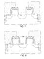
- FIG. 1shows an exemplary, conventional multi-FET structure 10 .
- the structure 10includes a number of components or regions that are overlying or embedded in a substrate (SUB) 12 .
- STI regions 14 and source/drain regions (S/D) 16are STI regions 14 and source/drain regions (S/D) 16 .
- the S/D 16lies below portions of the gates 18 .
- Each gateincludes a number of layers (not labeled), such as: a dielectric layer (e.g., silicon oxide) overlying the substrate, a poly layer overlying the dielectric layer and a cap layer (e.g., nitride) overlying the poly.
- SPAspacers
- the SPA 20 and the nitride capprotect the other layers of the gate 18 from undesired contacts and shorts.
- SILsilicide
- FIGS. 2-4illustrate a conventional technique for forming a borderless contact in the multi-FET structure of FIG. 1 .
- an interlevel dielectric (ILD) 24e.g., an oxide
- the contactis formed by patterning and RIE.
- the etched regionis filled with a metal at the CA 26 , as depicted in FIG. 4 .
- conventional techniquesmay result in a damaged spacer, for example, due to source/drain ion implantation, CA RIE or cleaning.
- a damaged spacercan cause electrical shorts between gate and CA contacts, for example.
- thick spacers for the silicide formation and a tight pitchmay result in a small CA space, leading to a more difficult CA fill.
- the nitride spacerhas a high parasitic capacitance, inhibiting operation of the final structure.
- Pitch scalingmeans there is a narrower space for the CA and a bordered contact will not work.
- Pitch scalingmeans there is a narrower space for the CA and a bordered contact will not work.
- conventional borderless contact techniqueshave various problems. Therefore, further techniques are needed that improve upon conventional borderless contact techniques.
- the exemplary embodiments of the inventionprovide a number of improvements over conventional borderless contacts and conventional borderless contact techniques. Some of the exemplary embodiments seek to address and improve upon the above-noted shortcomings in prior art systems.
- a first exemplary embodiment of the inventionprovides for replacement of the spacers after the contact via etch.
- the replacement spacersmay be low-k spacers to reduce the parasitic capacitance.
- the first exemplary embodimentalso provides for formation of a second set of spacers above the cap of the gate (e.g., above the nitride cap and adjacent to the ILD). This second set of spacers may also be low-k spacers.
- a second exemplary embodimentapplies a borderless contact technique to a gate-first metal/poly/silicide gate stack.
- a cap layere.g., a nitride cap
- a cap layeris removed in order to enable the formation of silicide on the gate structure (e.g., overlying a poly layer).
- Another cap layere.g., a nitride cap
- a third exemplary embodimentdescribes a borderless contact technique that is utilized with a gate-last metal gate.
- a dummy gateis formed and, after deposition and planarization of the ILD, removed.
- a replacement gate structureis then formed.
- the replacement gate structuremay comprise a layer of high-k dielectric that surrounds (e.g., surrounds or encompasses on all sides except for a surface that is substantially coplanar with a top surface of the structure) a metal gate.
- a cap layere.g., a nitride cap
- a fourth exemplary embodimentprovides for a borderless contact technique that is utilized with a FUSI gate.
- the cap layere.g., a nitride cap
- the FUSI gateis then formed and another cap layer (e.g., a nitride cap) is formed (e.g., by deposition and planarization).
- High-ksuch as a high-k dielectric
- Low-ksuch as a low-k dielectric
- Low-k dielectricrefers to a material (e.g., a dielectric) that has a relatively low dielectric constant, such as a dielectric constant less than 3.9 (the dielectric constant of silicon oxide), for example.
- Polyrefers to at least one of polycrystalline silicon, polycrystalline germanium and polycrystalline silicon germanium.
- a plurality of FETseach having a gate stack comprised of a plurality of layers, are formed in accordance with conventional processes (e.g., provision of a substrate, formation of isolation such as STIs, deposition of layers, patterning of the layers into gate stacks using photolithography and etching, formation of oxide and/or nitride spacers around the gate stacks (e.g., via deposition and etching or via oxide growth), ion implantation for the source/drain regions).
- the plurality of FETsmay be similar to those shown in FIG. 1 .
- the gate structuremay comprise: a dielectric layer (e.g., silicon oxide, silicon nitride, silicon oxynitride, a high-k dielectric material, or any suitable combination of such materials.) overlying the substrate, a poly layer overlying the dielectric layer and a cap layer (e.g., nitride) overlying the poly.
- a dielectric layere.g., silicon oxide, silicon nitride, silicon oxynitride, a high-k dielectric material, or any suitable combination of such materials.
- a dielectric layere.g., silicon oxide, silicon nitride, silicon oxynitride, a high-k dielectric material, or any suitable combination of such materials.
- a dielectric layere.g., silicon oxide, silicon nitride, silicon oxynitride, a high-k dielectric material, or any suitable combination of such materials.
- a cap layere.g., nitride
- An ILD 124(e.g., an oxide) is deposited, resulting in the structure shown in FIG. 5 .
- the contact viais formed, as illustrated in FIG. 6 , by patterning and etching (e.g., RIE). These processes may damage the spacers around the gate (e.g., the outer nitride spacers).
- the (possibly damaged) spacersare removed prior to filling the contact with metal (e.g., a metal-containing material). While FIG. 7 shows the removal of only the outer spacers (e.g., the outer nitride spacers), in other exemplary embodiments the inner spacers (e.g., the inner oxide spacers) are also removed.
- metale.g., a metal-containing material
- a selective etche.g., a wet etch process with an etch solution containing hydrofluoric/ethylene glycol (HF/EG) or hot phosphoric acid
- a dry etche.g., a chemical downstream etch process
- an etch selectivity greater than 5:1is achievable.
- a material other than nitridecan be used as the gate cap layer (e.g., silicon carbon).
- a non-selective nitride etchmay be performed.
- the nitride spacermay be about 200 A (about 200 angstroms) thick and the nitride gate cap may be about 400 A thick. Therefore, a 250 A nitride etch, even without selectivity, will completely remove the nitride spacer while leaving a nitride gate cap of about 150 A thickness.
- new replacement spacers 128are formed as shown in FIG. 8 .
- the new replacement spacers 128can be formed by any suitable technique, such as a film deposition process followed by a RIE process, for example.
- the replacement spacers 128may comprise any suitable insulating material including, but not limited to: silicon oxide, silicon nitride, silicon oxynitride, silicon carbide, a low-k material or any suitable combination of such materials.
- the replacement spacers 128may comprise a low-k material.
- Exemplary low-k dielectric materialsinclude organosilicate glass (OSG) and SiLKTM.
- the replacement spacers 128may be thinner than the original spacers. Formation of these new replacement spacers 128 cures potential defects in the original spacers, such as a pinhole, for example.
- an additional set of spacers 130may be formed. These additional spacers 130 are formed on the sidewalls of the ILD that is located above the gate structures, as illustrated in FIG. 9 .
- the etched regionis filled with conductive material (e.g., a metal, a metal-containing material, a material comprising a metal) at the CA 126 , as depicted in FIG. 10 .
- Forming the new replacement spacers 128 after the contact via etchprovides improved isolation between the contact and the gate.
- This exemplary techniquealso enables the usage of narrow spacers to facilitate the CA fill (i.e., a wide CA space) and the usage of low-k spacers to reduce parasitic capacitance.
- this exemplary techniquecan provide asymmetric spacers, for example, whereby the original (e.g., nitride) spacers covered by the ILD have a first thickness and the new replacement (e.g., low-k) spacers have a second thickness (e.g., that is thinner than the first thickness).
- a plurality of FETs(e.g., a multi-FET structure 210 ), each having a gate stack comprised of a plurality of layers, are formed in accordance with conventional processes (e.g., provision of a substrate, formation of STIs, deposition of layers, patterning of the layers into gate stacks using photolithography and etching, formation of oxide or nitride spacers around the gate stacks (e.g., via deposition and etching or via oxide growth), ion implantation for the source/drain regions).
- conventional processese.g., provision of a substrate, formation of STIs, deposition of layers, patterning of the layers into gate stacks using photolithography and etching, formation of oxide or nitride spacers around the gate stacks (e.g., via deposition and etching or via oxide growth), ion implantation for the source/drain regions).
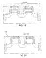
- FIG. 11shows an exemplary multi-FET structure 210 .
- the structure 210includes a number of components or regions that are overlying or embedded in a substrate (SUB) 212 .
- the S/D 216lie below portions of the gates 218 .
- Each gateincludes a number of layers as described further below.
- Surrounding each gate 218are spacers (SPA) 220 .
- the SPA 220 and the capprotect the other layers of the gate 218 from undesired contacts and shorts.
- SILsilicide
- FIG. 12shows an exemplary gate stack 218 for the multi-FET structure 210 of FIG. 11 .
- the exemplary gate stack 218includes: a high-k dielectric layer (HIGH-K) 230 overlying the SUB 212 , a metal layer (MET) 232 overlying the HIGH-K 230 , a poly layer (POLY) 234 overlying the HIGH-K 230 and a cap layer (CAP) 236 overlying the POLY 234 .
- the CAP 236may comprise a nitride cap or a nitride cap layer.
- the SPA 220 surrounding the gate 218are also shown in FIG. 12 .
- there may be a plurality of spacerse.g., an inner oxide spacer and an outer nitride spacer).
- An interlayer dielectric (ILD) 224such as an oxide with a nitride liner, for example, is deposited and planarized, resulting in the structure shown in FIG. 13 .
- the CAPs 236 on each gate (or at least one gate)are removed.
- a layer of silicide (SIL 2 ) 238is formed on each gate (i.e., each gate whose cap was removed).
- a new cap (CAP 2 ) 240is formed on each gate (i.e., each gate that received a layer of SIL 2 238 ).
- the CAP 2 240may be formed by deposition and planarization.
- the CAP 2 240may comprise a nitride cap.
- a second layer of ILD (ILD 2 ) 242is deposited and planarized.
- a contact mask (MASK) 244 and a contact RIEare used to remove the ILD material from between the gates 218 , thus forming the space for the borderless contact.
- the MASK 244is removed and the contact area (CA) 226 is formed, as illustrated in FIG. 19 , by filling the contact with conductive material, such as a metal, a metal-containing material or a material comprising a metal, as non-limiting examples.
- the opening on the MASK 244is wider than the space between the neighboring gates.
- the exemplary technique illustrated by FIGS. 11-19depict the formation of a borderless contact (e.g., in a MOSFET) with a gate-first metal gate capped by a low resistance poly/silicide layer 238 .
- the final structure of the gate stackincludes a high-k gate dielectric (HIGH-K 230 ) overlying the substrate (SUB 212 ), a metal layer (MET 232 ) overlying the high-k gate dielectric (HIGH-K 230 ), a poly layer (POLY 234 ) overlying the metal layer (MET 232 ), a silicide layer (SIL 2 238 ) overlying the poly layer (POLY 234 ) and an insulating cap layer (CAP 2 240 ) overlying the silicide layer (SIL 2 238 ).
- the borderless contactis isolated from the gate by a spacer(s) (SPA 220 ) and the insulating cap layer (CAP 2 240 ).
- a plurality of FETs(e.g., a multi-FET structure 310 as shown in FIG. 20 or a multi-FET structure 10 as shown in FIG. 1 ), each having a gate stack comprised of a plurality of layers, are formed in accordance with conventional processes (e.g., provision of a substrate, formation of STIs, deposition of layers, patterning of the layers into gate stacks using photolithography and etching, formation of oxide or nitride spacers around the gate stacks (e.g., via deposition and etching or via oxide growth), ion implantation for the source/drain regions).
- the plurality of FETsmay be similar to those shown in FIG.
- the gate structuremay comprise: a dielectric layer (e.g., silicon oxide) overlying the substrate, a poly layer overlying the dielectric layer and a cap layer (e.g., nitride) overlying the poly.
- a dielectric layere.g., silicon oxide
- a poly layeroverlying the dielectric layer
- a cap layere.g., nitride
- Surrounding each gateare spacers.
- Silicidemay be formed at the source/drain regions.
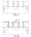
- the initial FETs of the third exemplary embodimentcomprise dummy gates. That is, since the third exemplary embodiment utilizes a gate-last technique, the initial gates are dummy gates (e.g., placeholders) that will be replaced at a later time (e.g., after deposition of the ILD). While the initial gates are dummy gates, they may be formed using similar (e.g., conventional) techniques.
- an interlayer dielectric (ILD) 324is deposited and planarized.
- the ILD 324may comprise an oxide with a nitride liner.
- the dummy gatesare removed, for example, via selective etching or other conventional techniques.
- a high-k dielectric (HKD) 330is deposited over the structure (e.g., the entire structure, including the ILD 324 ).
- a metal gate (MG) 332is deposited, planarized and recessed.
- the MG 332forms a metal gate core and is surrounded (e.g., adjacent) on at least two sides/surfaces by the dielectric (e.g., the HKD 330 is adjacent to at least sidewall surfaces and a bottom surface of the MG 332 ; the HKD 330 may not be adjacent to a top surface of the MG 332 ).
- the exposed portions of the HKD 330can be removed, resulting in the structure shown in FIG. 24 .
- a new cap (CAP 2 ) 340is formed on each gate (i.e., each gate for which a gate stack was formed in place of the removed dummy gate).
- the CAP 2 340may be formed by deposition and planarization.
- the CAP 2 340may comprise a nitride cap.
- a second layer of ILD (ILD 2 ) 342is deposited and planarized.
- a contact mask and a contact RIEare used to remove the ILD material from between the gates, thus forming the space for the borderless contact.
- the maskis removed and the contact area (CA) 326 is formed, as illustrated in FIG. 26 , by filling the contact with conductive material, such as a metal, a metal-containing material or a material comprising a metal, as non-limiting examples.
- the exemplary technique illustrated by FIGS. 20-26depict the formation of a borderless contact (e.g., in a MOSFET) with a gate-last gate (e.g., a metal gate).
- the final structure of the gate stackmay include a metal gate core (MG 332 ) that is surrounded (e.g., adjacent) on at least two sides/surfaces by a dielectric (e.g., a high-k dielectric such as HKD 330 , which is adjacent to at least sidewall surfaces and a bottom surface of the MG 332 ).
- the dielectricmay not be adjacent to a top surface of the metal gate core.
- the borderless contactis isolated from the gate by a spacer(s) and the insulating cap layer (CAP 2 340 ).
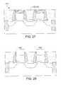
- a plurality of FETs(e.g., a multi-FET structure 410 as shown in FIG. 27 or a multi-FET structure 10 as shown in FIG. 1 ), each having a gate stack comprised of a plurality of layers, are formed in accordance with conventional processes (e.g., provision of a substrate, formation of STIs, deposition of layers, patterning of the layers into gate stacks using photolithography and etching, formation of oxide or nitride spacers around the gate stacks (e.g., via deposition and etching or via oxide growth), ion implantation for the source/drain regions).
- the plurality of FETsmay be similar to those shown in FIG.
- the gate structuremay comprise: a dielectric layer (e.g., silicon oxide) overlying the substrate, a poly layer overlying the dielectric layer and a cap layer (e.g., nitride) overlying the poly.
- a dielectric layere.g., silicon oxide
- a poly layeroverlying the dielectric layer
- a cap layere.g., nitride
- Surrounding each gateare spacers.
- Silicidemay be formed at the source/drain regions.
- an interlayer dielectric (ILD) 424is deposited and planarized.
- the ILD 424may comprise an oxide with a nitride liner.
- the cap layer (e.g., the nitride cap) on each gate stackis removed, resulting in an exposed gate stack 430 .
- the exposed gate stacks 430each may comprise a layer of gate dielectric (e.g., high-k dielectric material) overlying the substrate and a layer of polysilicon overlying the layer of gate dielectric.
- the cap layer(s)may be removed using a RIE.
- a FUSI gate (FG) 432is formed for each gate stack, as illustrated in FIG. 29 .
- the FG 432may be formed using processes and techniques that are known in the art. As a non-limiting example, the FG 432 may be formed using the techniques disclosed by Tan et al. in “Formation of a Thermally Stable NiSi FUSI Gate Electrode by a Novel Integration Process,” Mater. Res. Soc. Symp. Proc., Vol. 958 (0958-L06-08), 2007.
- a new cap (CAP 2 ) 440is formed on each gate (i.e., each gate for which a FG 432 was formed).
- the CAP 2 440may be formed by deposition and planarization.
- the CAP 2 340may comprise a nitride cap.
- a second layer of ILD (ILD 2 ) 442is deposited and planarized.
- a contact mask and a contact RIEare used to remove the ILD material from between the gates, thus forming the space for the borderless contact.
- the maskis removed and the contact area (CA) 426 is formed, as illustrated in FIG. 31 , by filling the contact with conductive material, such as a metal, a metal-containing material or a material comprising a metal, as non-limiting examples.
- FIGS. 27-31depict the formation of a borderless contact (e.g., in a MOSFET) with a FUSI gate (e.g., FG 432 ).
- the final structure of the gate stackincludes a FUSI gate structure (e.g., FG 432 ) that has a replacement or new cap layer (e.g., a nitride cap such as CAP 2 440 ).
- the borderless contactis isolated from the gate by a spacer(s) and the insulating cap layer (CAP 2 440 ).
- a method(e.g., to fabricate a semiconductor device having a borderless contact) comprising: forming a gate structure on a substrate ( 501 ); forming at least one first spacer around the gate structure ( 502 ); depositing an interlevel dielectric over the gate structure and the at least one first spacer ( 503 ); forming a contact area for the borderless contact by removing a portion of the interlevel dielectric, wherein removal of the portion of the interlevel dielectric exposes at least a portion of the at least one first spacer ( 504 ); removing the exposed portion of the at least one first spacer ( 505 ); forming at least one second spacer around the gate structure ( 506 ); and forming the borderless contact by filling the contact area with a material comprised of a metal ( 507 ).
- a method as in any above, where forming at least one first spacer around the gate structurecomprises forming the first spacer around the gate structure and forming a fourth spacer around the gate structure, where the fourth spacer comprises an inner spacer and the first spacer comprises an outer spacer.
- the at least one first spacercomprises a nitride and the at least one second spacer comprises a low-k dielectric material.
- a semiconductor devicecomprising: a substrate; a borderless contact comprised of a metal; a gate structure on the substrate; a first spacer disposed between the gate structure and the borderless contact and comprised of a first spacer material; an interlevel dielectric that at least partially overlies the gate structure; and a second spacer disposed between at least a portion of the gate structure and the interlevel dielectric and comprised of a second spacer material that is different from the first spacer material.
- the semiconductor device as abovefurther comprising a third spacer disposed on the gate structure and between the interlevel dielectric and the borderless contact.
- the semiconductor device as in any abovefurther comprising a fourth spacer disposed between the gate structure and the first spacer, where the fourth spacer comprises an inner spacer and the first spacer comprises an outer spacer.
- the semiconductor devicecomprises a metal oxide semiconductor field effect transistor.
- a method(e.g., to fabricate a semiconductor device having a borderless contact) comprising: forming a first gate structure on a substrate ( 601 ); depositing an interlevel dielectric over the first gate structure ( 602 ); planarizing the interlevel dielectric to expose a top surface of the first gate structure ( 603 ); removing at least a portion of the first gate structure ( 604 ); forming a second gate structure in place of the first gate structure ( 605 ); forming a contact area for the borderless contact by removing a portion of the interlevel dielectric ( 606 ); and forming the borderless contact by filling the contact area with a material comprised of a metal ( 607 ).
- a method as in any above, where the first gate structurecomprises a layer of dielectric material overlying the substrate, a layer comprised of polycrystalline silicon overlying the layer dielectric material and the first cap layer overlying the layer comprised of polycrystalline silicon.
- a method as in any above, where forming the second gate structurecomprises forming a second cap layer overlying the fully silicided gate.
- a method as in any above, where forming the contact area for the borderless contactcomprises depositing a second layer of interlevel dielectric and planarizing the second layer of interlevel dielectric.
- the interlevel dielectriccomprises an oxide with a nitride liner.
- the semiconductor devicecomprises a metal oxide semiconductor field effect transistor.
- a methodcomprising: forming a gate structure (GS) on a substrate (SUB), the gate structure comprising a layer of semiconductor material overlying the substrate, a layer comprised of a metal overlying the layer of semiconductor material, a layer comprised of polycrystalline silicon overlying the layer comprised of a metal and a first cap layer (CAP 1 ) overlying the layer comprised of polycrystalline silicon ( 701 ); depositing an interlevel dielectric (ILD) over the gate structure ( 702 ); planarizing the interlevel dielectric to expose a top surface of the gate structure ( 703 ); removing the first cap layer of the gate structure ( 704 ); forming a layer of silicide in the gate structure, the layer of silicide overlying the layer comprised of polycrystalline silicon ( 705 ); forming a second cap layer (CAP 2 ) in the gate structure, the
- the interlevel dielectriccomprises an oxide with a nitride liner.
- the second cap layercomprises a nitride.
- the borderless contactis disposed between the gate structure and another gate structure.
- a method as in any above, where forming the contact area for the borderless contactcomprises using a contact mask and a contact reactive ion etch to remove the portion of the interlevel dielectric, where an opening on the contact mask is wider than a space between the gate structure and the other gate structure.
- a semiconductor devicecomprising: a substrate; and a gate structure on the substrate, the gate structure comprising a layer of semiconductor material overlying the substrate, a layer comprised of a metal overlying the layer of semiconductor material, a layer comprised of polycrystalline silicon overlying the layer comprised of a metal, a layer of silicide overlying the layer comprised of polycrystalline silicon and a cap layer overlying the layer of silicide.
- a method(e.g., to fabricate a semiconductor device having a borderless contact) comprising: forming a dummy gate structure on a substrate ( 801 ); depositing an interlevel dielectric over the dummy gate structure ( 802 ); planarizing the interlevel dielectric to expose a top surface of the dummy gate structure ( 803 ); removing the dummy gate structure ( 804 ); forming a second gate structure in place of the dummy gate structure ( 805 ); forming a contact area for the borderless contact by removing a portion of the interlevel dielectric ( 806 ); and forming the borderless contact by filling the contact area with a material comprised of a metal ( 807 ).
- a method as above, where forming the second gate structure in place of the dummy gate structurecomprises: depositing a layer of dielectric material; depositing a material comprised of a metal; planarizing and recessing the material comprised of a metal to form a metal gate core in the second gate structure that is adjacent to the layer of dielectric material on at least two surfaces of the metal gate core; and forming a cap layer overlying the layer of dielectric material and the metal gate core.
- a method as in any above, where a top surface of the metal gate coreis not covered by the layer of dielectric material.
- the at least two surfacescomprise at least one sidewall surface and a bottom surface.
- a method as in any above, where the at least two surfacesdoes not comprise a top surface of the metal gate core.
- a semiconductor devicecomprising: a substrate; a gate structure on the substrate, the gate structure comprising a metal gate core that is adjacent to a layer of dielectric material on at least two surfaces of the metal gate core; and a cap layer overlying the layer of dielectric material and the metal gate core.
- the semiconductor device as in any abovewhere a top surface of the metal gate core is not covered by the layer of dielectric material.
- the semiconductor device as in any above, where the at least two surfacescomprise at least one sidewall surface and a bottom surface.
- the semiconductor device as in any abovewhere the at least two surfaces do not comprise a top surface of the metal gate core.
- a method(e.g., to fabricate a semiconductor device having a borderless contact) comprising: forming a gate structure on a substrate, the gate structure comprising a layer of dielectric material overlying the substrate, a layer comprised of polycrystalline silicon overlying the layer dielectric material and a first cap layer overlying the layer comprised of polycrystalline silicon ( 901 ); depositing an interlevel dielectric over the gate structure ( 902 ); planarizing the interlevel dielectric to expose a top surface of the gate structure ( 903 ); removing the first cap layer of the gate structure ( 904 ); forming a fully silicided gate in place of the gate structure ( 905 ); forming a second cap layer overlying the fully silicided gate ( 906 ); forming a contact area for the borderless contact by removing a portion of the interlevel dielectric ( 907 ); and forming the borderless contact by filling the contact area with a material comprised
- FIGS. 32-36further may be considered to correspond to one or more functions and/or operations that are performed in conjunction with one or more components, circuits, chips, apparatus, processors, computer programs and/or function blocks. Any and/or all of the above may be implemented in any practicable solution or arrangement that enables operation in accordance with the exemplary embodiments of the invention as described herein.
- FIGS. 32-36should be considered merely exemplary and non-limiting. It should be appreciated that the blocks shown in FIGS. 32 - 36 may correspond to one or more functions and/or operations that may be performed in any order (e.g., any suitable, practicable and/or feasible order) and/or concurrently (e.g., as suitable, practicable and/or feasible) so as to implement one or more of the exemplary embodiments of the invention. In addition, one or more additional functions, operations and/or steps may be utilized in conjunction with those shown in FIGS. 32-36 so as to implement one or more further exemplary embodiments of the invention.
- FIGS. 32-36may be utilized, implemented or practiced in conjunction with one or more further aspects in any combination (e.g., any combination that is suitable, practicable and/or feasible) and are not limited only to the steps, blocks, operations and/or functions shown in FIGS. 32-36 .
- each block in the flowchart or block diagramsmay represent a module, segment or portion of code, which comprises one or more executable instructions for implementing the specified (logical) function(s).
- the functions noted in the blockmay occur out of the order noted in the figures. For example, two blocks shown in succession may, in fact, be executed substantially concurrently, or the blocks may sometimes be executed in the reverse order, depending upon the functionality involved.
- the exemplary methods and techniques described hereinmay be used in the fabrication of integrated circuit chips.
- the resulting integrated circuit chipscan be distributed by the fabricator in raw wafer form (i.e., as a single wafer that has multiple unpackaged chips), as a bare die, or in a packaged form.
- the chipis mounted in a single chip package (e.g., a plastic carrier, with leads that are affixed to a motherboard or other higher level carrier) or in a multichip package (e.g., a ceramic carrier that has either or both surface interconnections or buried interconnections).
- the chipis then integrated with other chips, discrete circuit elements and/or other signal processing devices as part of either (a) an intermediate product, such as a motherboard, or (b) an end product.
- the end productcan be any product that includes integrated circuit chips, ranging from toys and other low-end applications to advanced computer products having numerous components, such as a display, a keyboard or other input device and/or a central processor, as non-limiting examples.
- depositingmay include any now known or later developed techniques appropriate for the material to be deposited, including, but not limited to: CVD, LPCVD, PECVD, semi-atmosphere CVD (SACVD), high density plasma CVD (HDPCVD), rapid thermal CVD (RTCVD), ultra-high vacuum CVD (UHVCVD), limited reaction processing CVD (LRPCVD), metalorganic CVD (MOCVD), sputtering deposition, ion beam deposition, electron beam deposition, laser assisted deposition, thermal oxidation, thermal nitridation, spin-on methods, physical vapor deposition (PVD), atomic level deposition (ALD), chemical oxidation, molecular beam epitaxy (MBE), plating or evaporation.
- CVDchemical vapor deposition
- PECVDsemi-atmosphere CVD
- SACVDhigh density plasma CVD
- HDPCVDhigh density plasma CVD
- RTCVDrapid thermal CVD
- UHVCVDultra-high
- connection or couplingshould be interpreted to indicate any such connection or coupling, direct or indirect, between the identified elements.
- one or more intermediate elementsmay be present between the “coupled” elements.
- the connection or coupling between the identified elementsmay be, as non-limiting examples, physical, electrical, magnetic, logical or any suitable combination thereof in accordance with the described exemplary embodiments.
- the connection or couplingmay comprise one or more printed electrical connections, wires, cables, mediums or any suitable combination thereof.
- various exemplary embodiments of the inventioncan be implemented in different mediums, such as software, hardware, logic, special purpose circuits or any combination thereof.
- some aspectsmay be implemented in software which may be run on a computing device, while other aspects may be implemented in hardware.
Landscapes
- Engineering & Computer Science (AREA)
- Physics & Mathematics (AREA)
- Condensed Matter Physics & Semiconductors (AREA)
- General Physics & Mathematics (AREA)
- Manufacturing & Machinery (AREA)
- Computer Hardware Design (AREA)
- Microelectronics & Electronic Packaging (AREA)
- Power Engineering (AREA)
- Insulated Gate Type Field-Effect Transistor (AREA)
- Internal Circuitry In Semiconductor Integrated Circuit Devices (AREA)
- Electrodes Of Semiconductors (AREA)
Abstract
Description
- The exemplary embodiments of this invention relate generally to semiconductor structures and, more specifically, relate to borderless contacts for semiconductor devices and the formation thereof.
- The following abbreviations are utilized herein:
- CA contact area
CD critical dimension
CMOS complementary metal-oxide semiconductor
CVD chemical vapor deposition
DRAM dynamic random access memory
FET field effect transistor
FUSI fully silicided
LPCVD low-pressure CVD
MOSFET metal oxide semiconductor field effect transistor - PECVD plasma-enhanced CVD
- RIE reactive ion etch
- STI shallow trench isolation
- Semiconductors and integrated circuit chips have become ubiquitous within many products due to their continually decreasing cost and size. In the microelectronics industry as well as in other industries involving construction of microscopic structures (e.g., micromachines, magnetoresistive heads, etc.) there is a continued desire to reduce the size of structural features and microelectronic devices and/or to provide a greater amount of circuitry for a given chip size. Miniaturization in general allows for increased performance (more processing per clock cycle and less heat generated) at lower power levels and lower cost. Present technology is at or approaching atomic level scaling of certain micro-devices such as logic gates, FETs and capacitors, for example. Circuit chips with hundreds of millions of such devices are not uncommon. Further size reductions appear to be approaching the physical limit of trace lines and micro-devices that are embedded upon and within their semiconductor substrates. The present invention is directed to such micro-sized devices.
- Basically, a FET is a transistor having a source, a gate, and a drain. The action of the FET depends on the flow of majority carriers along a channel between the source and drain that runs past the gate. Current through the channel, which is between the source and drain, is controlled by the transverse electric field under the gate. More than one gate (multi-gate) can be used to more effectively control the channel. The length of the gate determines how fast the FET switches, and can be about the same as the length of the channel (i.e., the distance between the source and drain). Multi-gate FETs are considered to be promising candidates to scale CMOS FET technology down to the sub-22 nm regime.
- The size of FETs has been successfully reduced through the use of one or more fin-shaped channels. A FET employing such a channel structure may be referred to as a FinFET. Previously, CMOS devices were substantially planar along the surface of the semiconductor substrate, the exception being the FET gate that was disposed over the top of the channel. Fins break from this paradigm by using a vertical channel structure in order to maximize the surface area of the channel that is exposed to the gate. The gate controls the channel more strongly because it extends over more than one side (surface) of the channel. For example, the gate can enclose three surfaces of the three-dimensional channel, rather than being disposed only across the top surface of the traditional planar channel.
- As the CDs of CMOS devices are being aggressively scaled, forming contacts on those small devices is becoming more and more difficult do to the tight overlay tolerance. Borderless contacts and techniques relating thereto help reduce the amount of space required for contacts, and enable production of smaller devices having a tighter pitch. Reference in regard to borderless contacts may be made to: commonly-assigned U.S. Pat. No. 4,944,682 to Cronin et al., commonly-assigned U.S. Pat. No. 4,966,870 to Barber et al. and commonly-assigned U.S. Pat. No. 5,759,867 to Armacost et al.
- Borderless contacts have been used in devices with tight pitch, particularly in memory products (e.g., DRAM). Reference in this regard is made to commonly assigned U.S. Pat. No. 6,709,926 to Chidambarrao et al. Borderless contacts are usually formed with a gate stack including a gate dielectric, a gate conductor and an insulating cap. The gate conductor usually comprises polycrystalline silicon (also referred to herein as “poly” or “polysilicon”). In some cases, metal or metal silicide is added on top of the poly in order to lower gate resistance. Reference in this regard may be made to U.S. Pat. No. 5,966,597 to Wright and U.S. Pat. No. 6,236,094 to Wright.
- High-k/metal or FUSI gates have been proposed and projected to fulfill future CMOS scaling. A MOSFET with a metal gate can be formed by either so-called “gate-first” techniques or “gate-last” techniques. In a gate-first technique, metal gates are deposited and patterned during gate formation. A poly cap layer on top of the metal layer is usually provided to achieve proper and stable workfunction of the gate stack. It is often further desired to form a silicide on top of the poly cap layer after source/drain formation in order to lower gate resistance. In a gate-last technique, a dummy gate is first formed in order to facilitate transistor formation. The dummy gate is replaced, usually by a high-k/metal gate, after source/drain formation. In a FUSI technique, a poly gate is first formed in order to facilitate transistor formation. The entire portion of the poly gate is then converted to silicide (e.g., after source/drain formation).
- In one exemplary embodiment of the invention, a semiconductor device comprising: a substrate; a borderless contact comprised of a metal; a gate structure on the substrate; a first spacer disposed between the gate structure and the borderless contact and comprised of a first spacer material; an interlevel dielectric that at least partially overlies the gate structure; and a second spacer disposed between at least a portion of the gate structure and the interlevel dielectric and comprised of a second spacer material that is different from the first spacer material.
- In another exemplary embodiment of the invention, a method (e.g., to fabricate a semiconductor device having a borderless contact) comprising: forming a first gate structure on a substrate; depositing an interlevel dielectric over the first gate structure; planarizing the interlevel dielectric to expose a top surface of the first gate structure; removing at least a portion of the first gate structure; forming a second gate structure in place of the first gate structure; forming a contact area for the borderless contact by removing a portion of the interlevel dielectric; and forming the borderless contact by filling the contact area with a material comprised of a metal.
- In a further exemplary embodiment of the invention, a semiconductor device comprising: a substrate; and a gate structure on the substrate, the gate structure comprising a layer of semiconductor material overlying the substrate, a layer comprised of a metal overlying the layer of semiconductor material, a layer comprised of polycrystalline silicon overlying the layer comprised of a metal, a layer of silicide overlying the layer comprised of polycrystalline silicon and a cap layer overlying the layer of silicide.
- In another exemplary embodiment of the invention, a semiconductor device comprising: a substrate; a gate structure on the substrate, the gate structure comprising a metal gate core that is adjacent to a layer of dielectric material on at least two surfaces of the metal gate core; and a cap layer overlying the layer of dielectric material and the metal gate core.
- The foregoing and other aspects of embodiments of this invention are made more evident in the following Detailed Description, when read in conjunction with the attached Drawing Figures, wherein:
FIG. 1 shows an exemplary, conventional multi-FET structure;FIGS. 2-4 illustrate a conventional technique for forming a borderless contact in the multi-FET structure ofFIG. 1 ;FIGS. 5-10 show a first technique for forming a borderless contact in a semiconductor device in accordance with a first exemplary embodiment of the invention;FIGS. 11-19 illustrate a second technique for forming a borderless contact in a semiconductor device in accordance with a second exemplary embodiment of the invention;FIGS. 20-26 depict a third technique for forming a borderless contact in a semiconductor device in accordance with a third exemplary embodiment of the invention;FIGS. 27-31 show a fourth technique for forming a borderless contact in a semiconductor device in accordance with a fourth exemplary embodiment of the invention;FIG. 32 depicts a flowchart illustrating one non-limiting example of a method for practicing the exemplary embodiments of this invention;FIG. 33 shows a flowchart illustrating another non-limiting example of a method for practicing the exemplary embodiments of this invention;FIG. 34 depicts a flowchart illustrating another non-limiting example of a method for practicing the exemplary embodiments of this invention;FIG. 35 shows a flowchart illustrating another non-limiting example of a method for practicing the exemplary embodiments of this invention; andFIG. 36 depicts a flowchart illustrating another non-limiting example of a method for practicing the exemplary embodiments of this invention.FIG. 1 shows an exemplary, conventionalmulti-FET structure 10. Thestructure 10 includes a number of components or regions that are overlying or embedded in a substrate (SUB)12. There areSTI regions 14 and source/drain regions (S/D)16. The S/D 16 lies below portions of thegates 18. Each gate includes a number of layers (not labeled), such as: a dielectric layer (e.g., silicon oxide) overlying the substrate, a poly layer overlying the dielectric layer and a cap layer (e.g., nitride) overlying the poly. Surrounding eachgate 18 are spacers (SPA)20. TheSPA 20 and the nitride cap protect the other layers of thegate 18 from undesired contacts and shorts. To reduce resistance, there may be a layer of silicide (SIL)22 over the S/D 16.FIGS. 2-4 illustrate a conventional technique for forming a borderless contact in the multi-FET structure ofFIG. 1 . As shown inFIG. 2 , an interlevel dielectric (ILD)24 (e.g., an oxide) is deposited over thestructure 10. InFIG. 3 , the contact is formed by patterning and RIE. To form the borderless contact, the etched region is filled with a metal at theCA 26, as depicted inFIG. 4 .- In some cases, conventional techniques may result in a damaged spacer, for example, due to source/drain ion implantation, CA RIE or cleaning. Such a damaged spacer can cause electrical shorts between gate and CA contacts, for example. Furthermore, thick spacers for the silicide formation and a tight pitch may result in a small CA space, leading to a more difficult CA fill. In addition, the nitride spacer has a high parasitic capacitance, inhibiting operation of the final structure.
- As noted above, device scaling results in a small space for forming the borderless contact. Pitch scaling means there is a narrower space for the CA and a bordered contact will not work. For example, consider a 22 nm node having a pitch of 80 nm, a gate length of about 25 nm and a spacer thickness of about 18 nm per side. This leaves about 19 nm of space for the CA (80−25−2×18=19) which is too small for a bordered contact. Furthermore, and also as noted above, conventional borderless contact techniques have various problems. Therefore, further techniques are needed that improve upon conventional borderless contact techniques.
- The exemplary embodiments of the invention provide a number of improvements over conventional borderless contacts and conventional borderless contact techniques. Some of the exemplary embodiments seek to address and improve upon the above-noted shortcomings in prior art systems.
- A first exemplary embodiment of the invention provides for replacement of the spacers after the contact via etch. As a non-limiting example, the replacement spacers may be low-k spacers to reduce the parasitic capacitance. The first exemplary embodiment also provides for formation of a second set of spacers above the cap of the gate (e.g., above the nitride cap and adjacent to the ILD). This second set of spacers may also be low-k spacers.
- Various further exemplary embodiments of the invention describe how at least a portion of the gate is removed after deposition and planarization of the ILD. A second exemplary embodiment applies a borderless contact technique to a gate-first metal/poly/silicide gate stack. A cap layer (e.g., a nitride cap) is removed in order to enable the formation of silicide on the gate structure (e.g., overlying a poly layer). Another cap layer (e.g., a nitride cap) is then formed (e.g., overlying the silicide layer) by deposition and planarization.
- A third exemplary embodiment describes a borderless contact technique that is utilized with a gate-last metal gate. A dummy gate is formed and, after deposition and planarization of the ILD, removed. A replacement gate structure is then formed. As a non-limiting example, the replacement gate structure may comprise a layer of high-k dielectric that surrounds (e.g., surrounds or encompasses on all sides except for a surface that is substantially coplanar with a top surface of the structure) a metal gate. A cap layer (e.g., a nitride cap) is subsequently formed by deposition and planarization.
- A fourth exemplary embodiment provides for a borderless contact technique that is utilized with a FUSI gate. After deposition and planarization of the ILD, the cap layer (e.g., a nitride cap) is removed (e.g., using a RIE). The FUSI gate is then formed and another cap layer (e.g., a nitride cap) is formed (e.g., by deposition and planarization).
- The exemplary embodiments of the invention and the various features and advantageous details thereof will be explained more fully with reference to the non-limiting exemplary embodiments that are illustrated in the accompanying drawings and detailed in the following description. It should be noted that the features illustrated in the drawings are not necessarily drawn to scale. Descriptions of well-known components and processing techniques (e.g., as known to one of ordinary skill in the art) are omitted so as to avoid unnecessarily obscuring the exemplary embodiments of the invention. The examples used herein are intended merely to facilitate an understanding of ways in which the exemplary embodiments of the invention may be practiced and to further enable those of ordinary skill in the art to practice the exemplary embodiments of the invention. Accordingly, the examples described herein should not be construed as limiting the scope of the exemplary embodiments of the invention.
- As utilized herein, the following terms should be accorded the specified definitions and/or meanings. It is believed that these definitions and meanings are in accord with the understanding of one of ordinary skill in the art. “High-k,” such as a high-k dielectric, refers to a material (e.g., a dielectric) that has a relatively high dielectric constant, such as a dielectric constant greater than 7 (the dielectric constant of silicon nitride), for example. “Low-k,” such as a low-k dielectric, refers to a material (e.g., a dielectric) that has a relatively low dielectric constant, such as a dielectric constant less than 3.9 (the dielectric constant of silicon oxide), for example. “Poly” refers to at least one of polycrystalline silicon, polycrystalline germanium and polycrystalline silicon germanium.
- In the first exemplary embodiment, a plurality of FETs, each having a gate stack comprised of a plurality of layers, are formed in accordance with conventional processes (e.g., provision of a substrate, formation of isolation such as STIs, deposition of layers, patterning of the layers into gate stacks using photolithography and etching, formation of oxide and/or nitride spacers around the gate stacks (e.g., via deposition and etching or via oxide growth), ion implantation for the source/drain regions). As a non-limiting example, the plurality of FETs may be similar to those shown in
FIG. 1 . For example, the gate structure may comprise: a dielectric layer (e.g., silicon oxide, silicon nitride, silicon oxynitride, a high-k dielectric material, or any suitable combination of such materials.) overlying the substrate, a poly layer overlying the dielectric layer and a cap layer (e.g., nitride) overlying the poly. Surrounding each gate are spacers. As non-limiting examples, the nitride cap may be formed using a LPCVD process (e.g., a LPCVD nitride) and the spacers may be formed using a PECVD process (e.g., a PECVD nitride). As a further non-limiting example, there may be a plurality of spacers (e.g., an inner oxide spacer and an outer nitride spacer). Silicide may be formed at the source/drain regions. - An ILD124 (e.g., an oxide) is deposited, resulting in the structure shown in
FIG. 5 . The contact via is formed, as illustrated inFIG. 6 , by patterning and etching (e.g., RIE). These processes may damage the spacers around the gate (e.g., the outer nitride spacers). - In accordance with the first exemplary embodiment, and as depicted in
FIG. 7 , the (possibly damaged) spacers are removed prior to filling the contact with metal (e.g., a metal-containing material). WhileFIG. 7 shows the removal of only the outer spacers (e.g., the outer nitride spacers), in other exemplary embodiments the inner spacers (e.g., the inner oxide spacers) are also removed. - As non-limiting examples, described below are several methods for removing damaged PECVD nitride spacers. A selective etch (e.g., a wet etch process with an etch solution containing hydrofluoric/ethylene glycol (HF/EG) or hot phosphoric acid) or a dry etch (e.g., a chemical downstream etch process) can be used to remove the PECVD nitride selective to the LPCVD nitride (of the nitride cap) and the ILD. As a further non-limiting example, an etch selectivity greater than 5:1 is achievable. Alternatively, a material other than nitride can be used as the gate cap layer (e.g., silicon carbon). As a further alternative, a non-selective nitride etch may be performed. In this case, one can rely on a thickness difference between the nitride spacer and the nitride gate cap to ensure preservation of the nitride gate cap. For example, the nitride spacer may be about 200 A (about 200 angstroms) thick and the nitride gate cap may be about 400 A thick. Therefore, a 250 A nitride etch, even without selectivity, will completely remove the nitride spacer while leaving a nitride gate cap of about 150 A thickness.
- After removal of the spacers,
new replacement spacers 128 are formed as shown inFIG. 8 . Thenew replacement spacers 128 can be formed by any suitable technique, such as a film deposition process followed by a RIE process, for example. The replacement spacers128 may comprise any suitable insulating material including, but not limited to: silicon oxide, silicon nitride, silicon oxynitride, silicon carbide, a low-k material or any suitable combination of such materials. As a non-limiting example, thereplacement spacers 128 may comprise a low-k material. Exemplary low-k dielectric materials include organosilicate glass (OSG) and SiLK™. Furthermore, thereplacement spacers 128 may be thinner than the original spacers. Formation of thesenew replacement spacers 128 cures potential defects in the original spacers, such as a pinhole, for example. - In conjunction with forming the
replacement spacers 128, an additional set ofspacers 130 may be formed. Theseadditional spacers 130 are formed on the sidewalls of the ILD that is located above the gate structures, as illustrated inFIG. 9 . To form the borderless contact, the etched region is filled with conductive material (e.g., a metal, a metal-containing material, a material comprising a metal) at theCA 126, as depicted inFIG. 10 . - Forming the
new replacement spacers 128 after the contact via etch provides improved isolation between the contact and the gate. This exemplary technique also enables the usage of narrow spacers to facilitate the CA fill (i.e., a wide CA space) and the usage of low-k spacers to reduce parasitic capacitance. In addition, this exemplary technique can provide asymmetric spacers, for example, whereby the original (e.g., nitride) spacers covered by the ILD have a first thickness and the new replacement (e.g., low-k) spacers have a second thickness (e.g., that is thinner than the first thickness). - In the second exemplary embodiment, a plurality of FETs (e.g., a multi-FET structure210), each having a gate stack comprised of a plurality of layers, are formed in accordance with conventional processes (e.g., provision of a substrate, formation of STIs, deposition of layers, patterning of the layers into gate stacks using photolithography and etching, formation of oxide or nitride spacers around the gate stacks (e.g., via deposition and etching or via oxide growth), ion implantation for the source/drain regions).
FIG. 11 shows an exemplarymulti-FET structure 210. Thestructure 210 includes a number of components or regions that are overlying or embedded in a substrate (SUB)212. There areSTI regions 214 and source/drain regions (S/D)216. The S/D 216 lie below portions of thegates 218. Each gate includes a number of layers as described further below. Surrounding eachgate 218 are spacers (SPA)220. TheSPA 220 and the cap protect the other layers of thegate 218 from undesired contacts and shorts. To reduce resistance, there may be a layer of silicide (SIL)222 over the S/D 216.FIG. 12 shows anexemplary gate stack 218 for themulti-FET structure 210 ofFIG. 11 . Theexemplary gate stack 218 includes: a high-k dielectric layer (HIGH-K)230 overlying theSUB 212, a metal layer (MET)232 overlying the HIGH-K 230, a poly layer (POLY)234 overlying the HIGH-K 230 and a cap layer (CAP)236 overlying thePOLY 234. As a non-limiting example, theCAP 236 may comprise a nitride cap or a nitride cap layer. For completeness, theSPA 220 surrounding thegate 218 are also shown inFIG. 12 . As a non-limiting example, there may be a plurality of spacers (e.g., an inner oxide spacer and an outer nitride spacer).- An interlayer dielectric (ILD)224, such as an oxide with a nitride liner, for example, is deposited and planarized, resulting in the structure shown in
FIG. 13 . Subsequently, and as shown inFIG. 14 , theCAPs 236 on each gate (or at least one gate) are removed. As depicted inFIG. 15 , a layer of silicide (SIL2)238 is formed on each gate (i.e., each gate whose cap was removed). As illustrated inFIG. 16 , a new cap (CAP2)240 is formed on each gate (i.e., each gate that received a layer of SIL2238). TheCAP2 240 may be formed by deposition and planarization. Furthermore, as a non-limiting example theCAP2 240 may comprise a nitride cap. Optionally, and as shown inFIG. 17 , a second layer of ILD (ILD2)242 is deposited and planarized. As shown inFIG. 18 , a contact mask (MASK)244 and a contact RIE are used to remove the ILD material from between thegates 218, thus forming the space for the borderless contact. TheMASK 244 is removed and the contact area (CA)226 is formed, as illustrated inFIG. 19 , by filling the contact with conductive material, such as a metal, a metal-containing material or a material comprising a metal, as non-limiting examples. In some exemplary embodiments, the opening on theMASK 244 is wider than the space between the neighboring gates. - The exemplary technique illustrated by
FIGS. 11-19 depict the formation of a borderless contact (e.g., in a MOSFET) with a gate-first metal gate capped by a low resistance poly/silicide layer 238. The final structure of the gate stack includes a high-k gate dielectric (HIGH-K230) overlying the substrate (SUB212), a metal layer (MET232) overlying the high-k gate dielectric (HIGH-K230), a poly layer (POLY234) overlying the metal layer (MET232), a silicide layer (SIL2238) overlying the poly layer (POLY234) and an insulating cap layer (CAP2240) overlying the silicide layer (SIL2238). The borderless contact is isolated from the gate by a spacer(s) (SPA220) and the insulating cap layer (CAP2240). - In the third exemplary embodiment, a plurality of FETs (e.g., a
multi-FET structure 310 as shown inFIG. 20 or amulti-FET structure 10 as shown inFIG. 1 ), each having a gate stack comprised of a plurality of layers, are formed in accordance with conventional processes (e.g., provision of a substrate, formation of STIs, deposition of layers, patterning of the layers into gate stacks using photolithography and etching, formation of oxide or nitride spacers around the gate stacks (e.g., via deposition and etching or via oxide growth), ion implantation for the source/drain regions). As a non-limiting example, the plurality of FETs may be similar to those shown inFIG. 1 . For example, the gate structure may comprise: a dielectric layer (e.g., silicon oxide) overlying the substrate, a poly layer overlying the dielectric layer and a cap layer (e.g., nitride) overlying the poly. Surrounding each gate are spacers. As a further non-limiting example, there may be a plurality of spacers (e.g., an inner oxide spacer and an outer nitride spacer). Silicide may be formed at the source/drain regions. - In comparison to the conventional FETs of
FIG. 1 and the first and second exemplary embodiments, the initial FETs of the third exemplary embodiment comprise dummy gates. That is, since the third exemplary embodiment utilizes a gate-last technique, the initial gates are dummy gates (e.g., placeholders) that will be replaced at a later time (e.g., after deposition of the ILD). While the initial gates are dummy gates, they may be formed using similar (e.g., conventional) techniques. - As shown in
FIG. 20 , an interlayer dielectric (ILD)324 is deposited and planarized. As a non-limiting example, theILD 324 may comprise an oxide with a nitride liner. Thereafter, and as illustrated inFIG. 21 , the dummy gates are removed, for example, via selective etching or other conventional techniques. As depicted inFIG. 22 , a high-k dielectric (HKD)330 is deposited over the structure (e.g., the entire structure, including the ILD324). Subsequently, and as shown inFIG. 23 , a metal gate (MG)332 is deposited, planarized and recessed. TheMG 332 forms a metal gate core and is surrounded (e.g., adjacent) on at least two sides/surfaces by the dielectric (e.g., theHKD 330 is adjacent to at least sidewall surfaces and a bottom surface of theMG 332; theHKD 330 may not be adjacent to a top surface of the MG332). As an optionally step, the exposed portions of theHKD 330 can be removed, resulting in the structure shown inFIG. 24 . - As illustrated in
FIG. 25 , a new cap (CAP2)340 is formed on each gate (i.e., each gate for which a gate stack was formed in place of the removed dummy gate). TheCAP2 340 may be formed by deposition and planarization. Furthermore, as a non-limiting example theCAP2 340 may comprise a nitride cap. Optionally, and as shown inFIG. 26 , a second layer of ILD (ILD2)342 is deposited and planarized. A contact mask and a contact RIE are used to remove the ILD material from between the gates, thus forming the space for the borderless contact. The mask is removed and the contact area (CA)326 is formed, as illustrated inFIG. 26 , by filling the contact with conductive material, such as a metal, a metal-containing material or a material comprising a metal, as non-limiting examples. - The exemplary technique illustrated by
FIGS. 20-26 depict the formation of a borderless contact (e.g., in a MOSFET) with a gate-last gate (e.g., a metal gate). As a non-limiting example, the final structure of the gate stack may include a metal gate core (MG332) that is surrounded (e.g., adjacent) on at least two sides/surfaces by a dielectric (e.g., a high-k dielectric such asHKD 330, which is adjacent to at least sidewall surfaces and a bottom surface of the MG332). The dielectric may not be adjacent to a top surface of the metal gate core. The borderless contact is isolated from the gate by a spacer(s) and the insulating cap layer (CAP2340). - In the fourth exemplary embodiment, a plurality of FETs (e.g., a
multi-FET structure 410 as shown inFIG. 27 or amulti-FET structure 10 as shown inFIG. 1 ), each having a gate stack comprised of a plurality of layers, are formed in accordance with conventional processes (e.g., provision of a substrate, formation of STIs, deposition of layers, patterning of the layers into gate stacks using photolithography and etching, formation of oxide or nitride spacers around the gate stacks (e.g., via deposition and etching or via oxide growth), ion implantation for the source/drain regions). As a non-limiting example, the plurality of FETs may be similar to those shown inFIG. 1 . For example, the gate structure may comprise: a dielectric layer (e.g., silicon oxide) overlying the substrate, a poly layer overlying the dielectric layer and a cap layer (e.g., nitride) overlying the poly. Surrounding each gate are spacers. As a further non-limiting example, there may be a plurality of spacers (e.g., an inner oxide spacer and an outer nitride spacer). Silicide may be formed at the source/drain regions. - As shown in
FIG. 27 , an interlayer dielectric (ILD)424 is deposited and planarized. As a non-limiting example, theILD 424 may comprise an oxide with a nitride liner. Thereafter, and as illustrated inFIG. 28 , the cap layer (e.g., the nitride cap) on each gate stack is removed, resulting in an exposedgate stack 430. As a non-limiting example, the exposedgate stacks 430 each may comprise a layer of gate dielectric (e.g., high-k dielectric material) overlying the substrate and a layer of polysilicon overlying the layer of gate dielectric. Also as a non-limiting example, the cap layer(s) may be removed using a RIE. - After the cap layer is removed for each gate in question, a FUSI gate (FG)432 is formed for each gate stack, as illustrated in
FIG. 29 . TheFG 432 may be formed using processes and techniques that are known in the art. As a non-limiting example, theFG 432 may be formed using the techniques disclosed by Tan et al. in “Formation of a Thermally Stable NiSi FUSI Gate Electrode by a Novel Integration Process,” Mater. Res. Soc. Symp. Proc., Vol. 958 (0958-L06-08), 2007. - As depicted in
FIG. 30 , a new cap (CAP2)440 is formed on each gate (i.e., each gate for which aFG 432 was formed). TheCAP2 440 may be formed by deposition and planarization. Furthermore, as a non-limiting example theCAP2 340 may comprise a nitride cap. Optionally, and as shown inFIG. 31 , a second layer of ILD (ILD2)442 is deposited and planarized. A contact mask and a contact RIE are used to remove the ILD material from between the gates, thus forming the space for the borderless contact. The mask is removed and the contact area (CA)426 is formed, as illustrated inFIG. 31 , by filling the contact with conductive material, such as a metal, a metal-containing material or a material comprising a metal, as non-limiting examples. - The exemplary technique illustrated by
FIGS. 27-31 depict the formation of a borderless contact (e.g., in a MOSFET) with a FUSI gate (e.g., FG432). As a non-limiting example, the final structure of the gate stack includes a FUSI gate structure (e.g., FG432) that has a replacement or new cap layer (e.g., a nitride cap such as CAP2440). The borderless contact is isolated from the gate by a spacer(s) and the insulating cap layer (CAP2440). - Below are further descriptions of various non-limiting, exemplary embodiments of the invention. The below-described exemplary embodiments are numbered separately for clarity purposes. This numbering should not be construed as entirely separating the various exemplary embodiments since aspects of one or more exemplary embodiments may be practiced in conjunction with one or more other aspects or exemplary embodiments.
- (1A) In one exemplary embodiment, and as shown in
FIG. 32 , a method (e.g., to fabricate a semiconductor device having a borderless contact) comprising: forming a gate structure on a substrate (501); forming at least one first spacer around the gate structure (502); depositing an interlevel dielectric over the gate structure and the at least one first spacer (503); forming a contact area for the borderless contact by removing a portion of the interlevel dielectric, wherein removal of the portion of the interlevel dielectric exposes at least a portion of the at least one first spacer (504); removing the exposed portion of the at least one first spacer (505); forming at least one second spacer around the gate structure (506); and forming the borderless contact by filling the contact area with a material comprised of a metal (507). - A method as above, further comprising: forming at least one third spacer above the gate structure and adjacent to the interlevel dielectric. A method as in any above, where forming at least one first spacer around the gate structure comprises forming the first spacer around the gate structure and forming a fourth spacer around the gate structure, where the fourth spacer comprises an inner spacer and the first spacer comprises an outer spacer. A method as in any above, where removing the exposed portion of the at least one first spacer does not result in removal of a portion of the fourth spacer. A method as in any above, where the at least one first spacer comprises a nitride and the at least one second spacer comprises a low-k dielectric material. A method as in any above, further comprising one or more additional aspects of the exemplary embodiments of the invention as described herein.
- (1B) In a further exemplary embodiment, a semiconductor device comprising: a substrate; a borderless contact comprised of a metal; a gate structure on the substrate; a first spacer disposed between the gate structure and the borderless contact and comprised of a first spacer material; an interlevel dielectric that at least partially overlies the gate structure; and a second spacer disposed between at least a portion of the gate structure and the interlevel dielectric and comprised of a second spacer material that is different from the first spacer material.
- The semiconductor device as above, further comprising a third spacer disposed on the gate structure and between the interlevel dielectric and the borderless contact. The semiconductor device as in any above, further comprising a fourth spacer disposed between the gate structure and the first spacer, where the fourth spacer comprises an inner spacer and the first spacer comprises an outer spacer. The semiconductor device as in any above, where the first spacer comprises a nitride and the second spacer comprises a low-k dielectric material. The semiconductor device as in any above, where the semiconductor device comprises a metal oxide semiconductor field effect transistor. The semiconductor device as in any above, further comprising one or more additional aspects of the exemplary embodiments of the invention as described herein.
- (2) In another exemplary embodiment, and as shown in
FIG. 33 , a method (e.g., to fabricate a semiconductor device having a borderless contact) comprising: forming a first gate structure on a substrate (601); depositing an interlevel dielectric over the first gate structure (602); planarizing the interlevel dielectric to expose a top surface of the first gate structure (603); removing at least a portion of the first gate structure (604); forming a second gate structure in place of the first gate structure (605); forming a contact area for the borderless contact by removing a portion of the interlevel dielectric (606); and forming the borderless contact by filling the contact area with a material comprised of a metal (607). - A method as above, where the first gate structure comprises a dummy gate structure and where removing the at least a portion of the first gate structure comprises removing substantially all of the dummy gate structure. A method as in any above, where the removed portion of the first gate structure comprises a first cap layer of the first gate structure. A method as in any above, where forming the second gate structure comprises forming a layer of silicide and forming a second cap layer. A method as in any above, where forming the second gate structure comprises forming a fully silicided gate structure. A method as in any above, where the first gate structure comprises a layer of dielectric material overlying the substrate, a layer comprised of polycrystalline silicon overlying the layer dielectric material and the first cap layer overlying the layer comprised of polycrystalline silicon. A method as in any above, where forming the second gate structure comprises forming a second cap layer overlying the fully silicided gate. A method as in any above, where forming the contact area for the borderless contact comprises depositing a second layer of interlevel dielectric and planarizing the second layer of interlevel dielectric. A method as in any above, where the interlevel dielectric comprises an oxide with a nitride liner. A method as in any above, where the semiconductor device comprises a metal oxide semiconductor field effect transistor. A method as in any above, further comprising one or more additional aspects of the exemplary embodiments of the invention as described herein.
- (3A) In another exemplary embodiment, and as shown in
FIG. 34 , a method (e.g., to fabricate a semiconductor device having a borderless contact) comprising: forming a gate structure (GS) on a substrate (SUB), the gate structure comprising a layer of semiconductor material overlying the substrate, a layer comprised of a metal overlying the layer of semiconductor material, a layer comprised of polycrystalline silicon overlying the layer comprised of a metal and a first cap layer (CAP1) overlying the layer comprised of polycrystalline silicon (701); depositing an interlevel dielectric (ILD) over the gate structure (702); planarizing the interlevel dielectric to expose a top surface of the gate structure (703); removing the first cap layer of the gate structure (704); forming a layer of silicide in the gate structure, the layer of silicide overlying the layer comprised of polycrystalline silicon (705); forming a second cap layer (CAP2) in the gate structure, the second cap layer overlying the layer of silicide (706); forming a contact area (CA) for the borderless contact by removing a portion of the interlevel dielectric (707); and forming the borderless contact by filling the contact area with a material comprised of a metal (708). - A method as above, where the interlevel dielectric comprises an oxide with a nitride liner. A method as in any above, where the second cap layer comprises a nitride. A method as in any above, where the borderless contact is disposed between the gate structure and another gate structure. A method as in any above, where forming the contact area for the borderless contact comprises using a contact mask and a contact reactive ion etch to remove the portion of the interlevel dielectric, where an opening on the contact mask is wider than a space between the gate structure and the other gate structure. A method as in any above, further comprising one or more additional aspects of the exemplary embodiments of the invention as described herein.
- (3B) In a further exemplary embodiment, a semiconductor device comprising: a substrate; and a gate structure on the substrate, the gate structure comprising a layer of semiconductor material overlying the substrate, a layer comprised of a metal overlying the layer of semiconductor material, a layer comprised of polycrystalline silicon overlying the layer comprised of a metal, a layer of silicide overlying the layer comprised of polycrystalline silicon and a cap layer overlying the layer of silicide.
- The semiconductor device as above, where the cap layer comprises a nitride. The semiconductor device as in any above, further comprising: an interlevel dielectric that at least partially overlies the gate structure; and a borderless contact comprised of a metal. The semiconductor device as in any above, where the interlevel dielectric comprises an oxide with a nitride liner. The semiconductor device as in any above, where the semiconductor device comprises a metal oxide semiconductor field effect transistor. The semiconductor device as in any above, further comprising one or more additional aspects of the exemplary embodiments of the invention as described herein.
- (4A) In another exemplary embodiment, and as shown in
FIG. 35 , a method (e.g., to fabricate a semiconductor device having a borderless contact) comprising: forming a dummy gate structure on a substrate (801); depositing an interlevel dielectric over the dummy gate structure (802); planarizing the interlevel dielectric to expose a top surface of the dummy gate structure (803); removing the dummy gate structure (804); forming a second gate structure in place of the dummy gate structure (805); forming a contact area for the borderless contact by removing a portion of the interlevel dielectric (806); and forming the borderless contact by filling the contact area with a material comprised of a metal (807). - A method as above, where forming the second gate structure in place of the dummy gate structure comprises: depositing a layer of dielectric material; depositing a material comprised of a metal; planarizing and recessing the material comprised of a metal to form a metal gate core in the second gate structure that is adjacent to the layer of dielectric material on at least two surfaces of the metal gate core; and forming a cap layer overlying the layer of dielectric material and the metal gate core. A method as in any above, where a top surface of the metal gate core is not covered by the layer of dielectric material. A method as in any above, where the at least two surfaces comprise at least one sidewall surface and a bottom surface. A method as in any above, where the at least two surfaces does not comprise a top surface of the metal gate core. A method as in any above, further comprising one or more additional aspects of the exemplary embodiments of the invention as described herein.
- (4B) In a further exemplary embodiment, a semiconductor device comprising: a substrate; a gate structure on the substrate, the gate structure comprising a metal gate core that is adjacent to a layer of dielectric material on at least two surfaces of the metal gate core; and a cap layer overlying the layer of dielectric material and the metal gate core.
- The semiconductor device as in any above, where a top surface of the metal gate core is not covered by the layer of dielectric material. The semiconductor device as in any above, where the at least two surfaces comprise at least one sidewall surface and a bottom surface.
- The semiconductor device as in any above, where the at least two surfaces do not comprise a top surface of the metal gate core. The semiconductor device as in any above, further comprising: an interlevel dielectric that at least partially overlies the gate structure; and a borderless contact comprised of a metal. The semiconductor device as in any above, further comprising one or more additional aspects of the exemplary embodiments of the invention as described herein.
- (5) In another exemplary embodiment, and as shown in
FIG. 36 , a method (e.g., to fabricate a semiconductor device having a borderless contact) comprising: forming a gate structure on a substrate, the gate structure comprising a layer of dielectric material overlying the substrate, a layer comprised of polycrystalline silicon overlying the layer dielectric material and a first cap layer overlying the layer comprised of polycrystalline silicon (901); depositing an interlevel dielectric over the gate structure (902); planarizing the interlevel dielectric to expose a top surface of the gate structure (903); removing the first cap layer of the gate structure (904); forming a fully silicided gate in place of the gate structure (905); forming a second cap layer overlying the fully silicided gate (906); forming a contact area for the borderless contact by removing a portion of the interlevel dielectric (907); and forming the borderless contact by filling the contact area with a material comprised of a metal (908). - A method as in any above, further comprising one or more additional aspects of the exemplary embodiments of the invention as described herein.
- The blocks shown in
FIGS. 32-36 further may be considered to correspond to one or more functions and/or operations that are performed in conjunction with one or more components, circuits, chips, apparatus, processors, computer programs and/or function blocks. Any and/or all of the above may be implemented in any practicable solution or arrangement that enables operation in accordance with the exemplary embodiments of the invention as described herein. - In addition, the arrangement of the blocks depicted in
FIGS. 32-36 should be considered merely exemplary and non-limiting. It should be appreciated that the blocks shown in FIGS.32-36 may correspond to one or more functions and/or operations that may be performed in any order (e.g., any suitable, practicable and/or feasible order) and/or concurrently (e.g., as suitable, practicable and/or feasible) so as to implement one or more of the exemplary embodiments of the invention. In addition, one or more additional functions, operations and/or steps may be utilized in conjunction with those shown inFIGS. 32-36 so as to implement one or more further exemplary embodiments of the invention. - That is, the exemplary embodiments of the invention shown in
FIGS. 32-36 may be utilized, implemented or practiced in conjunction with one or more further aspects in any combination (e.g., any combination that is suitable, practicable and/or feasible) and are not limited only to the steps, blocks, operations and/or functions shown inFIGS. 32-36 . - The flowchart and block diagrams in
FIGS. 32-36 illustrate the architecture, functionality, and operation of possible exemplary implementations of systems, methods and products according to various exemplary embodiments of the invention. In this regard, each block in the flowchart or block diagrams may represent a module, segment or portion of code, which comprises one or more executable instructions for implementing the specified (logical) function(s). It should also be noted that, in some alternative exemplary implementations, the functions noted in the block may occur out of the order noted in the figures. For example, two blocks shown in succession may, in fact, be executed substantially concurrently, or the blocks may sometimes be executed in the reverse order, depending upon the functionality involved. It will also be noted that each block of the block diagrams and/or flowchart illustration, and combinations of blocks in the block diagrams and/or flowchart illustration, can be implemented by special purpose hardware-based systems that perform the specified functions or acts, or combinations of special purpose hardware and computer instructions. - The exemplary methods and techniques described herein may be used in the fabrication of integrated circuit chips. The resulting integrated circuit chips can be distributed by the fabricator in raw wafer form (i.e., as a single wafer that has multiple unpackaged chips), as a bare die, or in a packaged form. In the latter case, the chip is mounted in a single chip package (e.g., a plastic carrier, with leads that are affixed to a motherboard or other higher level carrier) or in a multichip package (e.g., a ceramic carrier that has either or both surface interconnections or buried interconnections). The chip is then integrated with other chips, discrete circuit elements and/or other signal processing devices as part of either (a) an intermediate product, such as a motherboard, or (b) an end product. The end product can be any product that includes integrated circuit chips, ranging from toys and other low-end applications to advanced computer products having numerous components, such as a display, a keyboard or other input device and/or a central processor, as non-limiting examples.
- The terminology used herein is for the purpose of describing particular exemplary embodiments only and is not intended to be limiting of the exemplary embodiments of the invention. As used herein, the singular forms “a”, “an” and “the” are intended to include the plural forms as well, unless the context clearly indicates otherwise. It will be further understood that the terms “comprises” and/or “comprising,” when used in this specification, specify the presence of stated features, integers, steps, operations, elements and/or components, but do not preclude the presence or addition of one or more other features, integers, steps, operations, elements, components and/or groups thereof.
- Unless described otherwise herein, “depositing” may include any now known or later developed techniques appropriate for the material to be deposited, including, but not limited to: CVD, LPCVD, PECVD, semi-atmosphere CVD (SACVD), high density plasma CVD (HDPCVD), rapid thermal CVD (RTCVD), ultra-high vacuum CVD (UHVCVD), limited reaction processing CVD (LRPCVD), metalorganic CVD (MOCVD), sputtering deposition, ion beam deposition, electron beam deposition, laser assisted deposition, thermal oxidation, thermal nitridation, spin-on methods, physical vapor deposition (PVD), atomic level deposition (ALD), chemical oxidation, molecular beam epitaxy (MBE), plating or evaporation. Any references to “poly” or “poly silicon” should be understood to refer to polycrystalline silicon.
- Any use of the terms “connected,” “coupled” or variants thereof should be interpreted to indicate any such connection or coupling, direct or indirect, between the identified elements. As a non-limiting example, one or more intermediate elements may be present between the “coupled” elements. The connection or coupling between the identified elements may be, as non-limiting examples, physical, electrical, magnetic, logical or any suitable combination thereof in accordance with the described exemplary embodiments. As non-limiting examples, the connection or coupling may comprise one or more printed electrical connections, wires, cables, mediums or any suitable combination thereof.
- Generally, various exemplary embodiments of the invention can be implemented in different mediums, such as software, hardware, logic, special purpose circuits or any combination thereof. As a non-limiting example, some aspects may be implemented in software which may be run on a computing device, while other aspects may be implemented in hardware.
- The foregoing description has provided by way of exemplary and non-limiting examples a full and informative description of the best method and apparatus presently contemplated by the inventors for carrying out the invention. However, various modifications and adaptations may become apparent to those skilled in the relevant arts in view of the foregoing description, when read in conjunction with the accompanying drawings and the appended claims. However, all such and similar modifications will still fall within the scope of the teachings of the exemplary embodiments of the invention.
- Furthermore, some of the features of the preferred embodiments of this invention could be used to advantage without the corresponding use of other features. As such, the foregoing description should be considered as merely illustrative of the principles of the invention, and not in limitation thereof.
Claims (25)
Priority Applications (4)
| Application Number | Priority Date | Filing Date | Title |
|---|---|---|---|
| US12/617,084US8530971B2 (en) | 2009-11-12 | 2009-11-12 | Borderless contacts for semiconductor devices |
| PCT/EP2010/063808WO2011057839A1 (en) | 2009-11-12 | 2010-09-20 | Borderless contacts for semiconductor devices |
| US13/597,331US8450178B2 (en) | 2009-11-12 | 2012-08-29 | Borderless contacts for semiconductor devices |
| US13/894,733US8754488B2 (en) | 2009-11-12 | 2013-05-15 | Borderless contacts for semiconductor devices |
Applications Claiming Priority (1)
| Application Number | Priority Date | Filing Date | Title |
|---|---|---|---|
| US12/617,084US8530971B2 (en) | 2009-11-12 | 2009-11-12 | Borderless contacts for semiconductor devices |
Related Child Applications (2)
| Application Number | Title | Priority Date | Filing Date |
|---|---|---|---|
| US13/597,331DivisionUS8450178B2 (en) | 2009-11-12 | 2012-08-29 | Borderless contacts for semiconductor devices |
| US13/894,733ContinuationUS8754488B2 (en) | 2009-11-12 | 2013-05-15 | Borderless contacts for semiconductor devices |
Publications (2)
| Publication Number | Publication Date |
|---|---|
| US20110108930A1true US20110108930A1 (en) | 2011-05-12 |
| US8530971B2 US8530971B2 (en) | 2013-09-10 |
Family
ID=43127640
Family Applications (3)
| Application Number | Title | Priority Date | Filing Date |
|---|---|---|---|
| US12/617,084ActiveUS8530971B2 (en) | 2009-11-12 | 2009-11-12 | Borderless contacts for semiconductor devices |
| US13/597,331ActiveUS8450178B2 (en) | 2009-11-12 | 2012-08-29 | Borderless contacts for semiconductor devices |
| US13/894,733ActiveUS8754488B2 (en) | 2009-11-12 | 2013-05-15 | Borderless contacts for semiconductor devices |
Family Applications After (2)
| Application Number | Title | Priority Date | Filing Date |
|---|---|---|---|
| US13/597,331ActiveUS8450178B2 (en) | 2009-11-12 | 2012-08-29 | Borderless contacts for semiconductor devices |
| US13/894,733ActiveUS8754488B2 (en) | 2009-11-12 | 2013-05-15 | Borderless contacts for semiconductor devices |
Country Status (2)
| Country | Link |
|---|---|
| US (3) | US8530971B2 (en) |
| WO (1) | WO2011057839A1 (en) |
Cited By (48)
| Publication number | Priority date | Publication date | Assignee | Title |
|---|---|---|---|---|
| US20110193175A1 (en)* | 2010-02-09 | 2011-08-11 | Taiwan Semiconductor Manufacturing Co., Ltd. | Lower parasitic capacitance finfet |
| US20110254093A1 (en)* | 2009-12-29 | 2011-10-20 | Institute of Microelectronics, Chinese Academy of Sciences | Semiconductor device and method of manufacturing the same |
| US20110269303A1 (en)* | 2010-04-30 | 2011-11-03 | Globalfoundries Inc. | Reduced Defectivity in Contacts of a Semiconductor Device Comprising Replacement Gate Electrode Structures by Using an Intermediate Cap Layer |
| US8357978B1 (en)* | 2011-09-12 | 2013-01-22 | Globalfoundries Inc. | Methods of forming semiconductor devices with replacement gate structures |
| US20130043592A1 (en)* | 2011-08-19 | 2013-02-21 | Globalfoundries Inc. | Methods of Forming a Replacement Gate Comprised of Silicon and a Device Including Same |
| US20130043516A1 (en)* | 2011-08-16 | 2013-02-21 | Semiconductor Manufacturing International (Beijing) Corporation | Semiconductor Device and Manufacturing Method Thereof |
| WO2013089953A1 (en)* | 2011-12-16 | 2013-06-20 | International Business Machines Corporation | Rare-earth oxide isolated semiconductor fin |
| US20130178033A1 (en)* | 2009-12-30 | 2013-07-11 | Mark T. Bohr | Self-aligned contacts |
| US20130189833A1 (en)* | 2012-01-20 | 2013-07-25 | Globalfoundries Inc. | Method of Forming Self-Aligned Contacts for a Semiconductor Device |
| US20130270648A1 (en)* | 2012-04-13 | 2013-10-17 | Renesas Eletronics Corporation | Semiconductor devices with self-aligned source drain contacts and methods for making the same |
| US8575683B1 (en)* | 2012-05-16 | 2013-11-05 | United Microelectronics Corp. | Semiconductor device and method of fabricating the same |
| WO2014039166A1 (en)* | 2012-09-10 | 2014-03-13 | International Business Machines Corporation | Self-aligned contacts |
| US8679968B2 (en)* | 2012-05-15 | 2014-03-25 | Globalfoundries Singapore Pte. Ltd | Method for forming a self-aligned contact opening by a lateral etch |
| US8728927B1 (en) | 2012-12-10 | 2014-05-20 | International Business Machines Corporation | Borderless contacts for semiconductor transistors |
| CN103828057A (en)* | 2011-09-30 | 2014-05-28 | 英特尔公司 | Capping dielectric structure for transistor gates |
| US20150021683A1 (en)* | 2013-07-22 | 2015-01-22 | Globalfoundries Inc. | Methods of forming semiconductor device with self-aligned contact elements and the resulting devices |
| US8999795B2 (en) | 2013-07-18 | 2015-04-07 | International Business Machines Corporation | Asymmetrical replacement metal gate field effect transistor |
| US9041076B2 (en) | 2013-02-03 | 2015-05-26 | International Business Machines Corporation | Partial sacrificial dummy gate with CMOS device with high-k metal gate |
| US9093467B1 (en) | 2014-02-04 | 2015-07-28 | Globalfoundries Inc. | Methods of forming gate structures for semiconductor devices using a replacement gate technique and the resulting devices |
| US9147748B1 (en)* | 2014-05-01 | 2015-09-29 | Globalfoundries Inc. | Methods of forming replacement spacer structures on semiconductor devices |
| US9171925B2 (en)* | 2012-01-24 | 2015-10-27 | Taiwan Semiconductor Manufacturing Company, Ltd. | Multi-gate devices with replaced-channels and methods for forming the same |
| US9257348B2 (en) | 2013-08-06 | 2016-02-09 | Globalfoundries Inc. | Methods of forming replacement gate structures for transistors and the resulting devices |
| US9263330B2 (en) | 2014-01-10 | 2016-02-16 | Taiwan Semiconductor Manufacturing Company Limited | Semiconductor device, method for forming contact and method for etching continuous recess |
| US9281378B2 (en) | 2012-01-24 | 2016-03-08 | Taiwan Semiconductor Manufacturing Company, Ltd. | Fin recess last process for FinFET fabrication |
| US9349837B2 (en) | 2012-11-09 | 2016-05-24 | Taiwan Semiconductor Manufacturing Company, Ltd. | Recessing STI to increase Fin height in Fin-first process |
| US9425316B2 (en) | 2011-10-01 | 2016-08-23 | Intel Corporation | Source/drain contacts for non-planar transistors |
| US9443962B2 (en) | 2012-11-09 | 2016-09-13 | Taiwan Semiconductor Manufacturing Company, Ltd. | Recessing STI to increase fin height in fin-first process |
| US9466696B2 (en) | 2012-01-24 | 2016-10-11 | Taiwan Semiconductor Manufacturing Company, Ltd. | FinFETs and methods for forming the same |
| CN103828057B (en)* | 2011-09-30 | 2016-11-30 | 英特尔公司 | Capping Dielectric Structures for Transistor Gates |
| US9543426B2 (en)* | 2012-08-13 | 2017-01-10 | Globalfoundries Inc. | Semiconductor devices with self-aligned contacts and low-k spacers |
| US9543435B1 (en) | 2015-10-20 | 2017-01-10 | International Business Machines Corporation | Asymmetric multi-gate finFET |
| US9580776B2 (en) | 2011-09-30 | 2017-02-28 | Intel Corporation | Tungsten gates for non-planar transistors |
| US20170092740A1 (en)* | 2015-09-30 | 2017-03-30 | Taiwan Semiconductor Manufacturing Company, Ltd. | Metal Gate Scheme for Device and Methods of Forming |
| US9620619B2 (en) | 2012-01-12 | 2017-04-11 | Globalfoundries Inc. | Borderless contact structure |
| US9634124B2 (en) | 2011-12-06 | 2017-04-25 | Intel Corporation | Interlayer dielectric for non-planar transistors |
| US9659942B1 (en) | 2015-11-24 | 2017-05-23 | International Business Machines Corporation | Selective epitaxy growth for semiconductor devices with fin field-effect transistors (FinFET) |
| US9847398B1 (en)* | 2016-07-13 | 2017-12-19 | United Microelectronics Corp. | Semiconductor device with gate structure having dielectric layer on one side and contact plug on the other side |
| US10062763B2 (en)* | 2015-05-27 | 2018-08-28 | Qualcomm Incorporated | Method and apparatus for selectively forming nitride caps on metal gate |
| WO2018182627A1 (en)* | 2017-03-30 | 2018-10-04 | Intel Corporation | Transistors including asymmetric gate spacers |
| US20180350937A1 (en)* | 2016-12-30 | 2018-12-06 | United Microelectronics Corp. | Method for fabricating a semiconductor device |
| US20190123164A1 (en)* | 2015-07-17 | 2019-04-25 | Intel Corporation | Transistor with airgap spacer |
| EP3506367A1 (en)* | 2011-09-30 | 2019-07-03 | Intel Corporation | Tungsten gates for non-planar transistors |
| US20200020598A1 (en)* | 2014-10-02 | 2020-01-16 | International Business Machines Corporation | Semiconductor devices with sidewall spacers of equal thickness |
| US10573634B2 (en)* | 2017-06-09 | 2020-02-25 | Samsung Electronics Co., Ltd. | Semiconductor device |
| US20200126870A1 (en)* | 2018-10-22 | 2020-04-23 | Taiwan Semiconductor Manufacturing Co., Ltd. | Fusi gated device formation |
| TWI715674B (en)* | 2015-12-15 | 2021-01-11 | 台灣積體電路製造股份有限公司 | Fin-type field effect transistor device and manufacturing method thereof |
| US20210225707A1 (en)* | 2014-06-12 | 2021-07-22 | Taiwan Semiconductor Manufacturing Co., Ltd. | Self-Aligned Interconnect with Protection Layer |
| US11476258B2 (en)* | 2013-09-17 | 2022-10-18 | Renesas Electronics Corporation | Semiconductor device including short-circuit prevention structure and manufacturing method thereof |
Families Citing this family (17)
| Publication number | Priority date | Publication date | Assignee | Title |
|---|---|---|---|---|
| US20120205727A1 (en)* | 2011-02-11 | 2012-08-16 | International Business Machines Corporation | Semiconductor device including multiple metal semiconductor alloy region and a gate structure covered by a continuous encapsulating layer |
| US8440533B2 (en)* | 2011-03-04 | 2013-05-14 | Globalfoundries Singapore Pte. Ltd. | Self-aligned contact for replacement metal gate and silicide last processes |
| US9034703B2 (en) | 2012-09-13 | 2015-05-19 | International Business Machines Corporation | Self aligned contact with improved robustness |
| US8871582B2 (en) | 2013-03-15 | 2014-10-28 | Globalfoundries Inc. | Methods of forming a semiconductor device with a protected gate cap layer and the resulting device |
| US8906754B2 (en)* | 2013-03-15 | 2014-12-09 | Globalfoundries Inc. | Methods of forming a semiconductor device with a protected gate cap layer and the resulting device |
| US9117886B2 (en) | 2013-11-27 | 2015-08-25 | United Microelectronics Corp. | Method for fabricating a semiconductor device by forming and removing a dummy gate structure |
| US9412656B2 (en)* | 2014-02-14 | 2016-08-09 | Taiwan Semiconductor Manufacturing Co., Ltd. | Reverse tone self-aligned contact |
| US9543407B2 (en) | 2014-02-27 | 2017-01-10 | International Business Machines Corporation | Low-K spacer for RMG finFET formation |
| US9711646B2 (en) | 2014-03-31 | 2017-07-18 | United Microelectronics Corp. | Semiconductor structure and manufacturing method for the same |
| TWI612563B (en) | 2014-07-07 | 2018-01-21 | 聯華電子股份有限公司 | Metal gate structure and manufacturing method thereof |
| US10084085B2 (en) | 2015-06-11 | 2018-09-25 | Taiwan Semiconductor Manufacturing Co., Ltd. | Fin field effect transistor (FinFET) device structure with stop layer and method for forming the same |
| US10622457B2 (en) | 2015-10-09 | 2020-04-14 | International Business Machines Corporation | Forming replacement low-K spacer in tight pitch fin field effect transistors |
| US9831119B2 (en) | 2015-12-28 | 2017-11-28 | Samsung Electronics Co., Ltd. | Semiconductor device and method of fabricating the same |
| US9530887B1 (en)* | 2016-02-25 | 2016-12-27 | Taiwan Semiconductor Manufacturing Co., Ltd. | Fin-type field effect transistor device and manufacturing method thereof |
| US9985107B2 (en) | 2016-06-29 | 2018-05-29 | International Business Machines Corporation | Method and structure for forming MOSFET with reduced parasitic capacitance |
| CN108346577B (en)* | 2017-01-22 | 2021-04-09 | 中芯国际集成电路制造(上海)有限公司 | Semiconductor device and method of manufacturing the same |
| US11569370B2 (en)* | 2019-06-27 | 2023-01-31 | Intel Corporation | DEPOP using cyclic selective spacer etch |
Citations (56)
| Publication number | Priority date | Publication date | Assignee | Title |
|---|---|---|---|---|
| US4944682A (en)* | 1988-10-07 | 1990-07-31 | International Business Machines Corporation | Method of forming borderless contacts |
| US4966870A (en)* | 1988-04-14 | 1990-10-30 | International Business Machines Corporation | Method for making borderless contacts |
| US5102815A (en)* | 1990-12-19 | 1992-04-07 | Intel Corporation | Method of fabricating a composite inverse T-gate metal oxide semiconductor device |
| US5651857A (en)* | 1995-09-08 | 1997-07-29 | International Business Machines Corporation | Sidewall spacer using an overhang |
| US5759867A (en)* | 1995-04-21 | 1998-06-02 | International Business Machines Corporation | Method of making a disposable corner etch stop-spacer for borderless contacts |
| US5965462A (en)* | 1997-10-27 | 1999-10-12 | Mosel Vitelic, Inc. | Method for forming a gate structure used in borderless contact etching |
| US5966597A (en)* | 1998-01-06 | 1999-10-12 | Altera Corporation | Method of forming low resistance gate electrodes |
| US6013553A (en)* | 1997-07-24 | 2000-01-11 | Texas Instruments Incorporated | Zirconium and/or hafnium oxynitride gate dielectric |
| US6037223A (en)* | 1998-10-23 | 2000-03-14 | Taiwan Semiconductor Manufacturing Company, Ltd. | Stack gate flash memory cell featuring symmetric self aligned contact structures |
| US6096595A (en)* | 1999-05-12 | 2000-08-01 | Taiwan Semiconductor Manufacturing Company | Integration of a salicide process for MOS logic devices, and a self-aligned contact process for MOS memory devices |
| US6103608A (en)* | 1998-04-20 | 2000-08-15 | United Integrated Circuit Corp. | Method of forming a contact window |
| US6130121A (en)* | 1998-10-19 | 2000-10-10 | United Semiconductor Corp. | Method for fabricating a transistor |
| US6194748B1 (en)* | 1999-05-03 | 2001-02-27 | Advanced Micro Devices, Inc. | MOSFET with suppressed gate-edge fringing field effect |
| US6207514B1 (en)* | 1999-01-04 | 2001-03-27 | International Business Machines Corporation | Method for forming borderless gate structures and apparatus formed thereby |
| US6228731B1 (en)* | 1999-08-16 | 2001-05-08 | Taiwan Semiconductor Manufacturing Company | Re-etched spacer process for a self-aligned structure |
| US6235593B1 (en)* | 1999-02-18 | 2001-05-22 | Taiwan Semiconductor Manufacturing Company | Self aligned contact using spacers on the ILD layer sidewalls |
| US6235627B1 (en)* | 1997-06-30 | 2001-05-22 | Kabushiki Kaisha Toshiba | Semiconductor device and method for manufacturing the same |
| US6255205B1 (en)* | 1997-08-06 | 2001-07-03 | Mosel Vitelic, Inc. | High density programmable read-only memory employing double-wall spacers |
| US6261911B1 (en)* | 1999-02-13 | 2001-07-17 | Hyundai Electronics Industries Co., Ltd. | Method of manufacturing a junction in a semiconductor device |
| US6265271B1 (en)* | 2000-01-24 | 2001-07-24 | Taiwan Semiconductor Manufacturing Company | Integration of the borderless contact salicide process |
| US20010010961A1 (en)* | 2000-01-27 | 2001-08-02 | Soon Moon Jung | Method of forming contact holes of semiconductor device |
| US6274468B1 (en)* | 1998-07-06 | 2001-08-14 | United Microelectronics Corp. | Method of manufacturing borderless contact |
| US6380063B1 (en)* | 2000-03-01 | 2002-04-30 | International Business Machines Corporation | Raised wall isolation device with spacer isolated contacts and the method of so forming |
| US6403423B1 (en)* | 2000-11-15 | 2002-06-11 | International Business Machines Corporation | Modified gate processing for optimized definition of array and logic devices on same chip |
| US6406987B1 (en)* | 1998-09-08 | 2002-06-18 | Taiwan Semiconductor Manufacturing Company | Method for making borderless contacts to active device regions and overlaying shallow trench isolation regions |
| US6466656B1 (en)* | 1998-12-02 | 2002-10-15 | Eci Telecom Ltd. | System employing XDSL spectrum relocation |
| US20020179982A1 (en)* | 2001-05-29 | 2002-12-05 | United Microelectronics Corp. | MOS field effect transistor structure and method of manufacture |
| US20020190316A1 (en)* | 2001-06-19 | 2002-12-19 | Samsung Electronics, Co., Ltd. | Semiconductor device with borderless contact structure and method of manufacturing the same |
| US6501131B1 (en)* | 1999-07-22 | 2002-12-31 | International Business Machines Corporation | Transistors having independently adjustable parameters |
| US20030001200A1 (en)* | 2001-06-29 | 2003-01-02 | International Business Machines Corporation | Modified vertical MOSFET and methods of formation thereof |
| US6531724B1 (en)* | 1999-01-04 | 2003-03-11 | International Business Machines Corporation | Borderless gate structures |
| US6613637B1 (en)* | 2002-05-31 | 2003-09-02 | Lsi Logic Corporation | Composite spacer scheme with low overlapped parasitic capacitance |
| US20030224573A1 (en)* | 2002-05-31 | 2003-12-04 | International Business Machines Corporation | High performance logic and high density embedded dram with borderless contact and antispacer |
| US20040033659A1 (en)* | 2000-12-19 | 2004-02-19 | Mihel Seitz | Method for fabricating transistors having damascene formed gate contacts and self-aligned borderless bit line contacts |
| US6696333B1 (en)* | 1999-11-30 | 2004-02-24 | Intel Corporation | Method of making integrated circuit with MOSFETs having bi-layer metal gate electrodes |
| US6720213B1 (en)* | 2003-01-15 | 2004-04-13 | International Business Machines Corporation | Low-K gate spacers by fluorine implantation |
| US6724051B1 (en)* | 2000-10-05 | 2004-04-20 | Advanced Micro Devices, Inc. | Nickel silicide process using non-reactive spacer |
| US20040155282A1 (en)* | 2003-02-11 | 2004-08-12 | Kim Hyoung-Sub | Semiconductor device having self-aligned contact hole and method of fabricating the same |
| US6791190B1 (en)* | 2003-05-09 | 2004-09-14 | Macronix International Co., Ltd. | Self-aligned contact/borderless contact opening and method for forming same |
| US6798017B2 (en)* | 2001-08-31 | 2004-09-28 | International Business Machines Corporation | Vertical dual gate field effect transistor |
| US20050045865A1 (en)* | 2003-08-25 | 2005-03-03 | Yu-Piao Wang | [semiconductor device and fabricating method thereof] |
| US20060084273A1 (en)* | 1996-07-12 | 2006-04-20 | Kabushiki Kaisha Toshiba | Semiconductor device using damascene technique and manufacturing method therefor |
| US7037774B1 (en)* | 2004-10-21 | 2006-05-02 | Integrated Device Technology, Inc. | Self-aligned contact structure and process for forming self-aligned contact structure |
| US7053444B2 (en)* | 2002-08-29 | 2006-05-30 | Micron Technology, Inc. | Method and apparatus for a flash memory device comprising a source local interconnect |
| US7074666B2 (en)* | 2004-07-28 | 2006-07-11 | International Business Machines Corporation | Borderless contact structures |
| US20060166432A1 (en)* | 2005-01-25 | 2006-07-27 | International Business Machines Corporation | Process for oxide cap formation in semiconductor manufacturing |
| US7138685B2 (en)* | 2002-12-11 | 2006-11-21 | International Business Machines Corporation | Vertical MOSFET SRAM cell |
| US7259049B2 (en)* | 2002-12-23 | 2007-08-21 | International Business Machines Corporation | Self-aligned isolation double-gate FET |
| US20070262451A1 (en)* | 2006-05-09 | 2007-11-15 | Willy Rachmady | Recessed workfunction metal in CMOS transistor gates |
| US20070281410A1 (en)* | 2006-06-05 | 2007-12-06 | Chartered Semiconductor Manufacturing, Ltd | Spacer-less low-k dielectric processes |
| US20080029834A1 (en)* | 2006-08-07 | 2008-02-07 | Bernhard Sell | Low-k isolation spacers for conductive regions |
| US20080093681A1 (en)* | 2006-10-20 | 2008-04-24 | Yoshihiro Sato | Semiconductor device and method for fabricating the same |
| US7365378B2 (en)* | 2005-03-31 | 2008-04-29 | International Business Machines Corporation | MOSFET structure with ultra-low K spacer |
| US20080230906A1 (en)* | 2007-03-22 | 2008-09-25 | Keith Kwong Hon Wong | Contact structure having dielectric spacer and method |
| US20090057730A1 (en)* | 2007-09-05 | 2009-03-05 | International Business Machines Corporation | Methods for forming self-aligned borderless contacts for strain engineered logic devices and structure thereof |
| US7659213B2 (en)* | 2006-04-28 | 2010-02-09 | GlobalFoundries, Inc. | Transistor having an embedded tensile strain layer with reduced offset to the gate electrode and a method for forming the same |
Family Cites Families (2)
| Publication number | Priority date | Publication date | Assignee | Title |
|---|---|---|---|---|
| EP0967640A3 (en) | 1998-06-25 | 2000-01-05 | Siemens Aktiengesellschaft | Method of making a self-aligned contact |
| KR100336574B1 (en) | 2000-06-21 | 2002-05-16 | 박종섭 | Method of manufacturing semiconductor device |
- 2009
- 2009-11-12USUS12/617,084patent/US8530971B2/enactiveActive
- 2010
- 2010-09-20WOPCT/EP2010/063808patent/WO2011057839A1/enactiveApplication Filing
- 2012
- 2012-08-29USUS13/597,331patent/US8450178B2/enactiveActive
- 2013
- 2013-05-15USUS13/894,733patent/US8754488B2/enactiveActive
Patent Citations (66)
| Publication number | Priority date | Publication date | Assignee | Title |
|---|---|---|---|---|
| US4966870A (en)* | 1988-04-14 | 1990-10-30 | International Business Machines Corporation | Method for making borderless contacts |
| US4944682A (en)* | 1988-10-07 | 1990-07-31 | International Business Machines Corporation | Method of forming borderless contacts |
| US5102815A (en)* | 1990-12-19 | 1992-04-07 | Intel Corporation | Method of fabricating a composite inverse T-gate metal oxide semiconductor device |
| US5759867A (en)* | 1995-04-21 | 1998-06-02 | International Business Machines Corporation | Method of making a disposable corner etch stop-spacer for borderless contacts |
| US5651857A (en)* | 1995-09-08 | 1997-07-29 | International Business Machines Corporation | Sidewall spacer using an overhang |
| US20060084273A1 (en)* | 1996-07-12 | 2006-04-20 | Kabushiki Kaisha Toshiba | Semiconductor device using damascene technique and manufacturing method therefor |
| US6235627B1 (en)* | 1997-06-30 | 2001-05-22 | Kabushiki Kaisha Toshiba | Semiconductor device and method for manufacturing the same |
| US6013553A (en)* | 1997-07-24 | 2000-01-11 | Texas Instruments Incorporated | Zirconium and/or hafnium oxynitride gate dielectric |
| US6255205B1 (en)* | 1997-08-06 | 2001-07-03 | Mosel Vitelic, Inc. | High density programmable read-only memory employing double-wall spacers |
| US5965462A (en)* | 1997-10-27 | 1999-10-12 | Mosel Vitelic, Inc. | Method for forming a gate structure used in borderless contact etching |
| US5966597A (en)* | 1998-01-06 | 1999-10-12 | Altera Corporation | Method of forming low resistance gate electrodes |
| US6236094B1 (en)* | 1998-01-06 | 2001-05-22 | Altera Corporation | Low resistance gate electrodes |
| US6103608A (en)* | 1998-04-20 | 2000-08-15 | United Integrated Circuit Corp. | Method of forming a contact window |
| US6274468B1 (en)* | 1998-07-06 | 2001-08-14 | United Microelectronics Corp. | Method of manufacturing borderless contact |
| US6406987B1 (en)* | 1998-09-08 | 2002-06-18 | Taiwan Semiconductor Manufacturing Company | Method for making borderless contacts to active device regions and overlaying shallow trench isolation regions |
| US6130121A (en)* | 1998-10-19 | 2000-10-10 | United Semiconductor Corp. | Method for fabricating a transistor |
| US6037223A (en)* | 1998-10-23 | 2000-03-14 | Taiwan Semiconductor Manufacturing Company, Ltd. | Stack gate flash memory cell featuring symmetric self aligned contact structures |
| US6466656B1 (en)* | 1998-12-02 | 2002-10-15 | Eci Telecom Ltd. | System employing XDSL spectrum relocation |
| US6531724B1 (en)* | 1999-01-04 | 2003-03-11 | International Business Machines Corporation | Borderless gate structures |
| US6207514B1 (en)* | 1999-01-04 | 2001-03-27 | International Business Machines Corporation | Method for forming borderless gate structures and apparatus formed thereby |
| US6261911B1 (en)* | 1999-02-13 | 2001-07-17 | Hyundai Electronics Industries Co., Ltd. | Method of manufacturing a junction in a semiconductor device |
| US6235593B1 (en)* | 1999-02-18 | 2001-05-22 | Taiwan Semiconductor Manufacturing Company | Self aligned contact using spacers on the ILD layer sidewalls |
| US6194748B1 (en)* | 1999-05-03 | 2001-02-27 | Advanced Micro Devices, Inc. | MOSFET with suppressed gate-edge fringing field effect |
| US6096595A (en)* | 1999-05-12 | 2000-08-01 | Taiwan Semiconductor Manufacturing Company | Integration of a salicide process for MOS logic devices, and a self-aligned contact process for MOS memory devices |
| US6501131B1 (en)* | 1999-07-22 | 2002-12-31 | International Business Machines Corporation | Transistors having independently adjustable parameters |
| US6228731B1 (en)* | 1999-08-16 | 2001-05-08 | Taiwan Semiconductor Manufacturing Company | Re-etched spacer process for a self-aligned structure |
| US6696333B1 (en)* | 1999-11-30 | 2004-02-24 | Intel Corporation | Method of making integrated circuit with MOSFETs having bi-layer metal gate electrodes |
| US6265271B1 (en)* | 2000-01-24 | 2001-07-24 | Taiwan Semiconductor Manufacturing Company | Integration of the borderless contact salicide process |
| US20010010961A1 (en)* | 2000-01-27 | 2001-08-02 | Soon Moon Jung | Method of forming contact holes of semiconductor device |
| US6335279B2 (en)* | 2000-01-27 | 2002-01-01 | Samsung Electronics Co., Ltd. | Method of forming contact holes of semiconductor device |
| US6380063B1 (en)* | 2000-03-01 | 2002-04-30 | International Business Machines Corporation | Raised wall isolation device with spacer isolated contacts and the method of so forming |
| US6724051B1 (en)* | 2000-10-05 | 2004-04-20 | Advanced Micro Devices, Inc. | Nickel silicide process using non-reactive spacer |
| US20020111025A1 (en)* | 2000-11-15 | 2002-08-15 | International Business Machines Corporation | Modified gate processing for optimized difinition of array and logic devices on same chip |
| US6548357B2 (en)* | 2000-11-15 | 2003-04-15 | International Business Machines Corporation | Modified gate processing for optimized definition of array and logic devices on same chip |
| US6403423B1 (en)* | 2000-11-15 | 2002-06-11 | International Business Machines Corporation | Modified gate processing for optimized definition of array and logic devices on same chip |
| US6812092B2 (en)* | 2000-12-19 | 2004-11-02 | Infineon Technologies | Method for fabricating transistors having damascene formed gate contacts and self-aligned borderless bit line contacts |
| US20040033659A1 (en)* | 2000-12-19 | 2004-02-19 | Mihel Seitz | Method for fabricating transistors having damascene formed gate contacts and self-aligned borderless bit line contacts |
| US20020179982A1 (en)* | 2001-05-29 | 2002-12-05 | United Microelectronics Corp. | MOS field effect transistor structure and method of manufacture |
| US20020190316A1 (en)* | 2001-06-19 | 2002-12-19 | Samsung Electronics, Co., Ltd. | Semiconductor device with borderless contact structure and method of manufacturing the same |
| US20050045968A1 (en)* | 2001-06-19 | 2005-03-03 | Kwean Sung-Un | Semiconductor device with borderless contact structure and method of manufacturing the same |
| US20030001200A1 (en)* | 2001-06-29 | 2003-01-02 | International Business Machines Corporation | Modified vertical MOSFET and methods of formation thereof |
| US6541810B2 (en)* | 2001-06-29 | 2003-04-01 | International Business Machines Corporation | Modified vertical MOSFET and methods of formation thereof |
| US6798017B2 (en)* | 2001-08-31 | 2004-09-28 | International Business Machines Corporation | Vertical dual gate field effect transistor |
| US6709926B2 (en)* | 2002-05-31 | 2004-03-23 | International Business Machines Corporation | High performance logic and high density embedded dram with borderless contact and antispacer |
| US20040075111A1 (en)* | 2002-05-31 | 2004-04-22 | Dureseti Chidambarrao | High performance logic and high density embedded dram with borderless contact and antispacer |
| US20030224573A1 (en)* | 2002-05-31 | 2003-12-04 | International Business Machines Corporation | High performance logic and high density embedded dram with borderless contact and antispacer |
| US6613637B1 (en)* | 2002-05-31 | 2003-09-02 | Lsi Logic Corporation | Composite spacer scheme with low overlapped parasitic capacitance |
| US6873010B2 (en)* | 2002-05-31 | 2005-03-29 | International Business Machines Corporation | High performance logic and high density embedded dram with borderless contact and antispacer |
| US7053444B2 (en)* | 2002-08-29 | 2006-05-30 | Micron Technology, Inc. | Method and apparatus for a flash memory device comprising a source local interconnect |
| US7138685B2 (en)* | 2002-12-11 | 2006-11-21 | International Business Machines Corporation | Vertical MOSFET SRAM cell |
| US7259049B2 (en)* | 2002-12-23 | 2007-08-21 | International Business Machines Corporation | Self-aligned isolation double-gate FET |
| US6720213B1 (en)* | 2003-01-15 | 2004-04-13 | International Business Machines Corporation | Low-K gate spacers by fluorine implantation |
| US20040155282A1 (en)* | 2003-02-11 | 2004-08-12 | Kim Hyoung-Sub | Semiconductor device having self-aligned contact hole and method of fabricating the same |
| US6791190B1 (en)* | 2003-05-09 | 2004-09-14 | Macronix International Co., Ltd. | Self-aligned contact/borderless contact opening and method for forming same |
| US20050045865A1 (en)* | 2003-08-25 | 2005-03-03 | Yu-Piao Wang | [semiconductor device and fabricating method thereof] |
| US7074666B2 (en)* | 2004-07-28 | 2006-07-11 | International Business Machines Corporation | Borderless contact structures |
| US7037774B1 (en)* | 2004-10-21 | 2006-05-02 | Integrated Device Technology, Inc. | Self-aligned contact structure and process for forming self-aligned contact structure |
| US20060166432A1 (en)* | 2005-01-25 | 2006-07-27 | International Business Machines Corporation | Process for oxide cap formation in semiconductor manufacturing |
| US7365378B2 (en)* | 2005-03-31 | 2008-04-29 | International Business Machines Corporation | MOSFET structure with ultra-low K spacer |
| US7659213B2 (en)* | 2006-04-28 | 2010-02-09 | GlobalFoundries, Inc. | Transistor having an embedded tensile strain layer with reduced offset to the gate electrode and a method for forming the same |
| US20070262451A1 (en)* | 2006-05-09 | 2007-11-15 | Willy Rachmady | Recessed workfunction metal in CMOS transistor gates |
| US20070281410A1 (en)* | 2006-06-05 | 2007-12-06 | Chartered Semiconductor Manufacturing, Ltd | Spacer-less low-k dielectric processes |
| US20080029834A1 (en)* | 2006-08-07 | 2008-02-07 | Bernhard Sell | Low-k isolation spacers for conductive regions |
| US20080093681A1 (en)* | 2006-10-20 | 2008-04-24 | Yoshihiro Sato | Semiconductor device and method for fabricating the same |
| US20080230906A1 (en)* | 2007-03-22 | 2008-09-25 | Keith Kwong Hon Wong | Contact structure having dielectric spacer and method |
| US20090057730A1 (en)* | 2007-09-05 | 2009-03-05 | International Business Machines Corporation | Methods for forming self-aligned borderless contacts for strain engineered logic devices and structure thereof |
Cited By (110)
| Publication number | Priority date | Publication date | Assignee | Title |
|---|---|---|---|---|
| US8222099B2 (en)* | 2009-12-29 | 2012-07-17 | Institute of Microelectronics, Chinese Academy of Sciences | Semiconductor device and method of manufacturing the same |
| US20110254093A1 (en)* | 2009-12-29 | 2011-10-20 | Institute of Microelectronics, Chinese Academy of Sciences | Semiconductor device and method of manufacturing the same |
| US20210134673A1 (en)* | 2009-12-30 | 2021-05-06 | Intel Corporation | Self-aligned contacts |
| US10930557B2 (en)* | 2009-12-30 | 2021-02-23 | Intel Corporation | Self-aligned contacts |
| US12266571B2 (en) | 2009-12-30 | 2025-04-01 | Intel Corporation | Self-aligned contacts |
| US9093513B2 (en)* | 2009-12-30 | 2015-07-28 | Intel Corporation | Self-aligned contacts |
| US20150270216A1 (en)* | 2009-12-30 | 2015-09-24 | Intel Corporation | Self-aligned contacts |
| US11600524B2 (en)* | 2009-12-30 | 2023-03-07 | Intel Corporation | Self-aligned contacts |
| US10629483B2 (en)* | 2009-12-30 | 2020-04-21 | Intel Corporation | Self-aligned contacts |
| US10141226B2 (en) | 2009-12-30 | 2018-11-27 | Intel Corporation | Self-aligned contacts |
| US20130178033A1 (en)* | 2009-12-30 | 2013-07-11 | Mark T. Bohr | Self-aligned contacts |
| US20190051558A1 (en)* | 2009-12-30 | 2019-02-14 | Intel Corporation | Self-aligned contacts |
| US9892967B2 (en) | 2009-12-30 | 2018-02-13 | Intel Corporation | Self-aligned contacts |
| US9466565B2 (en)* | 2009-12-30 | 2016-10-11 | Intel Corporation | Self-aligned contacts |
| US11887891B2 (en) | 2009-12-30 | 2024-01-30 | Intel Corporation | Self-aligned contacts |
| US9508821B2 (en) | 2009-12-30 | 2016-11-29 | Intel Corporation | Self-aligned contacts |
| US8697539B2 (en) | 2010-02-09 | 2014-04-15 | Taiwan Semiconductor Manufacturing Co., Ltd. | Method of making lower parasitic capacitance FinFET |
| US8362572B2 (en)* | 2010-02-09 | 2013-01-29 | Taiwan Semiconductor Manufacturing Co., Ltd. | Lower parasitic capacitance FinFET |
| US20110193175A1 (en)* | 2010-02-09 | 2011-08-11 | Taiwan Semiconductor Manufacturing Co., Ltd. | Lower parasitic capacitance finfet |
| US8183139B2 (en)* | 2010-04-30 | 2012-05-22 | Globalfoundries Inc. | Reduced defectivity in contacts of a semiconductor device comprising replacement gate electrode structures by using an intermediate cap layer |
| US20110269303A1 (en)* | 2010-04-30 | 2011-11-03 | Globalfoundries Inc. | Reduced Defectivity in Contacts of a Semiconductor Device Comprising Replacement Gate Electrode Structures by Using an Intermediate Cap Layer |
| US20130043516A1 (en)* | 2011-08-16 | 2013-02-21 | Semiconductor Manufacturing International (Beijing) Corporation | Semiconductor Device and Manufacturing Method Thereof |
| US8877651B2 (en)* | 2011-08-16 | 2014-11-04 | Semiconductor Manufacturing International (Beijing) Corporation | Semiconductor device and manufacturing method involving multilayer contact etch stop |
| US20130043592A1 (en)* | 2011-08-19 | 2013-02-21 | Globalfoundries Inc. | Methods of Forming a Replacement Gate Comprised of Silicon and a Device Including Same |
| US8742510B2 (en) | 2011-09-12 | 2014-06-03 | Globalfoundries Inc. | Semiconductor devices with replacement gate structures having conductive contacts positioned therebetween |
| US8357978B1 (en)* | 2011-09-12 | 2013-01-22 | Globalfoundries Inc. | Methods of forming semiconductor devices with replacement gate structures |
| US9580776B2 (en) | 2011-09-30 | 2017-02-28 | Intel Corporation | Tungsten gates for non-planar transistors |
| US9490347B2 (en)* | 2011-09-30 | 2016-11-08 | Intel Corporation | Capping dielectric structures for transistor gates |
| CN107039527A (en)* | 2011-09-30 | 2017-08-11 | 英特尔公司 | Cap dielectric structure for transistor gate |
| EP2761664A4 (en)* | 2011-09-30 | 2015-06-17 | Intel Corp | DIELECTRIC RECOVERY STRUCTURE FOR TRANSISTOR GRIDS |
| US9812546B2 (en) | 2011-09-30 | 2017-11-07 | Intel Corporation | Tungsten gates for non-planar transistors |
| EP3506367A1 (en)* | 2011-09-30 | 2019-07-03 | Intel Corporation | Tungsten gates for non-planar transistors |
| CN103828057B (en)* | 2011-09-30 | 2016-11-30 | 英特尔公司 | Capping Dielectric Structures for Transistor Gates |
| US20160049499A1 (en)* | 2011-09-30 | 2016-02-18 | Intel Corporation | Capping dielectric structures for transistor gates |
| CN103828057A (en)* | 2011-09-30 | 2014-05-28 | 英特尔公司 | Capping dielectric structure for transistor gates |
| US10020375B2 (en) | 2011-09-30 | 2018-07-10 | Intel Corporation | Tungsten gates for non-planar transistors |
| US9637810B2 (en) | 2011-09-30 | 2017-05-02 | Intel Corporation | Tungsten gates for non-planar transistors |
| US9202699B2 (en) | 2011-09-30 | 2015-12-01 | Intel Corporation | Capping dielectric structure for transistor gates |
| US20230028568A1 (en)* | 2011-10-01 | 2023-01-26 | Intel Corporation | Source/drain contacts for non-planar transistors |
| US9853156B2 (en) | 2011-10-01 | 2017-12-26 | Intel Corporation | Source/drain contacts for non-planar transistors |
| US10283640B2 (en) | 2011-10-01 | 2019-05-07 | Intel Corporation | Source/drain contacts for non-planar transistors |
| US10770591B2 (en) | 2011-10-01 | 2020-09-08 | Intel Corporation | Source/drain contacts for non-planar transistors |
| US9425316B2 (en) | 2011-10-01 | 2016-08-23 | Intel Corporation | Source/drain contacts for non-planar transistors |
| US9634124B2 (en) | 2011-12-06 | 2017-04-25 | Intel Corporation | Interlayer dielectric for non-planar transistors |
| US10056488B2 (en) | 2011-12-06 | 2018-08-21 | Intel Corporation | Interlayer dielectric for non-planar transistors |
| US8853781B2 (en) | 2011-12-16 | 2014-10-07 | International Business Machines Corporation | Rare-earth oxide isolated semiconductor fin |
| JP2015508567A (en)* | 2011-12-16 | 2015-03-19 | インターナショナル・ビジネス・マシーンズ・コーポレーションInternational Business Machines Corporation | Semiconductor structure and manufacturing method thereof (rare earth oxide separation type semiconductor fin) |
| WO2013089953A1 (en)* | 2011-12-16 | 2013-06-20 | International Business Machines Corporation | Rare-earth oxide isolated semiconductor fin |
| US9058987B2 (en) | 2011-12-16 | 2015-06-16 | International Business Machines Corporation | Rare-earth oxide isolated semiconductor fin |
| US9620619B2 (en) | 2012-01-12 | 2017-04-11 | Globalfoundries Inc. | Borderless contact structure |
| US20130189833A1 (en)* | 2012-01-20 | 2013-07-25 | Globalfoundries Inc. | Method of Forming Self-Aligned Contacts for a Semiconductor Device |
| US8927407B2 (en)* | 2012-01-20 | 2015-01-06 | Globalfoundries Inc. | Method of forming self-aligned contacts for a semiconductor device |
| US9466696B2 (en) | 2012-01-24 | 2016-10-11 | Taiwan Semiconductor Manufacturing Company, Ltd. | FinFETs and methods for forming the same |
| US9281378B2 (en) | 2012-01-24 | 2016-03-08 | Taiwan Semiconductor Manufacturing Company, Ltd. | Fin recess last process for FinFET fabrication |
| US10014223B2 (en) | 2012-01-24 | 2018-07-03 | Taiwan Semiconductor Manufacturing Company, Ltd. | Multi-gate devices with replaced-channels and methods for forming the same |
| US9171925B2 (en)* | 2012-01-24 | 2015-10-27 | Taiwan Semiconductor Manufacturing Company, Ltd. | Multi-gate devices with replaced-channels and methods for forming the same |
| US10121851B2 (en) | 2012-01-24 | 2018-11-06 | Taiwan Semiconductor Manufacturing Company, Ltd. | Fin recess last process for FinFET fabrication |
| US20130270648A1 (en)* | 2012-04-13 | 2013-10-17 | Renesas Eletronics Corporation | Semiconductor devices with self-aligned source drain contacts and methods for making the same |
| US9111783B2 (en)* | 2012-04-13 | 2015-08-18 | Renesas Electronics Corporation | Semiconductor devices with self-aligned source drain contacts and methods for making the same |
| US10978355B2 (en) | 2012-04-26 | 2021-04-13 | Taiwan Semiconductor Manufacturing Company, Ltd. | Multi-gate devices with replaced-channels and methods for forming the same |
| US8679968B2 (en)* | 2012-05-15 | 2014-03-25 | Globalfoundries Singapore Pte. Ltd | Method for forming a self-aligned contact opening by a lateral etch |
| US8575683B1 (en)* | 2012-05-16 | 2013-11-05 | United Microelectronics Corp. | Semiconductor device and method of fabricating the same |
| US9543426B2 (en)* | 2012-08-13 | 2017-01-10 | Globalfoundries Inc. | Semiconductor devices with self-aligned contacts and low-k spacers |
| WO2014039166A1 (en)* | 2012-09-10 | 2014-03-13 | International Business Machines Corporation | Self-aligned contacts |
| US8853076B2 (en) | 2012-09-10 | 2014-10-07 | International Business Machines Corporation | Self-aligned contacts |
| US9299795B2 (en) | 2012-10-28 | 2016-03-29 | International Business Machines Corporation | Partial sacrificial dummy gate with CMOS device with high-k metal gate |
| US9443962B2 (en) | 2012-11-09 | 2016-09-13 | Taiwan Semiconductor Manufacturing Company, Ltd. | Recessing STI to increase fin height in fin-first process |
| US9349837B2 (en) | 2012-11-09 | 2016-05-24 | Taiwan Semiconductor Manufacturing Company, Ltd. | Recessing STI to increase Fin height in Fin-first process |
| US10269933B2 (en) | 2012-11-09 | 2019-04-23 | Taiwan Semiconductor Manufacturing Company, Ltd. | Recessing STI to increase Fin height in Fin-first process |
| US11114550B2 (en) | 2012-11-09 | 2021-09-07 | Taiwan Semiconductor Manufacturing Company, Ltd. | Recessing STI to increase FIN height in FIN-first process |
| US11121213B2 (en) | 2012-11-09 | 2021-09-14 | Taiwan Semiconductor Manufacturing Company, Ltd. | Fin recess last process for FinFET fabrication |
| US11682697B2 (en) | 2012-11-09 | 2023-06-20 | Taiwan Semiconductor Manufacturing Company, Ltd. | Fin recess last process for FinFET fabrication |
| US8728927B1 (en) | 2012-12-10 | 2014-05-20 | International Business Machines Corporation | Borderless contacts for semiconductor transistors |
| US9041076B2 (en) | 2013-02-03 | 2015-05-26 | International Business Machines Corporation | Partial sacrificial dummy gate with CMOS device with high-k metal gate |
| US8999795B2 (en) | 2013-07-18 | 2015-04-07 | International Business Machines Corporation | Asymmetrical replacement metal gate field effect transistor |
| US20150021683A1 (en)* | 2013-07-22 | 2015-01-22 | Globalfoundries Inc. | Methods of forming semiconductor device with self-aligned contact elements and the resulting devices |
| US9153498B2 (en)* | 2013-07-22 | 2015-10-06 | Globalfoundries Inc. | Methods of forming semiconductor device with self-aligned contact elements and the resulting devices |
| US9953978B2 (en) | 2013-08-06 | 2018-04-24 | Globalfoundries Inc. | Replacement gate structures for transistor devices |
| US9257348B2 (en) | 2013-08-06 | 2016-02-09 | Globalfoundries Inc. | Methods of forming replacement gate structures for transistors and the resulting devices |
| US11476258B2 (en)* | 2013-09-17 | 2022-10-18 | Renesas Electronics Corporation | Semiconductor device including short-circuit prevention structure and manufacturing method thereof |
| US9263330B2 (en) | 2014-01-10 | 2016-02-16 | Taiwan Semiconductor Manufacturing Company Limited | Semiconductor device, method for forming contact and method for etching continuous recess |
| US9431507B2 (en) | 2014-02-04 | 2016-08-30 | Globalfoundries Inc. | Replacement gate structure with low-K sidewall spacer for semiconductor devices |
| US9093467B1 (en) | 2014-02-04 | 2015-07-28 | Globalfoundries Inc. | Methods of forming gate structures for semiconductor devices using a replacement gate technique and the resulting devices |
| US9496354B2 (en) | 2014-05-01 | 2016-11-15 | Globalfoundries Inc. | Semiconductor devices with dummy gate structures partially on isolation regions |
| US9147748B1 (en)* | 2014-05-01 | 2015-09-29 | Globalfoundries Inc. | Methods of forming replacement spacer structures on semiconductor devices |
| US12009258B2 (en)* | 2014-06-12 | 2024-06-11 | Taiwan Semiconductor Manufacturing Company, Ltd. | Self-aligned interconnect with protection layer |
| US20210225707A1 (en)* | 2014-06-12 | 2021-07-22 | Taiwan Semiconductor Manufacturing Co., Ltd. | Self-Aligned Interconnect with Protection Layer |
| US20200020598A1 (en)* | 2014-10-02 | 2020-01-16 | International Business Machines Corporation | Semiconductor devices with sidewall spacers of equal thickness |
| US10062763B2 (en)* | 2015-05-27 | 2018-08-28 | Qualcomm Incorporated | Method and apparatus for selectively forming nitride caps on metal gate |
| US20190123164A1 (en)* | 2015-07-17 | 2019-04-25 | Intel Corporation | Transistor with airgap spacer |
| US11114538B2 (en)* | 2015-07-17 | 2021-09-07 | Intel Corporation | Transistor with an airgap spacer adjacent to a transistor gate |
| US9871114B2 (en)* | 2015-09-30 | 2018-01-16 | Taiwan Semiconductor Manufacturing Company, Ltd. | Metal gate scheme for device and methods of forming |
| US20170092740A1 (en)* | 2015-09-30 | 2017-03-30 | Taiwan Semiconductor Manufacturing Company, Ltd. | Metal Gate Scheme for Device and Methods of Forming |
| US11127836B2 (en) | 2015-09-30 | 2021-09-21 | Taiwan Semiconductor Manufacturing Company, Ltd. | Metal gate scheme for device and methods of forming |
| US10283619B2 (en) | 2015-09-30 | 2019-05-07 | Taiwan Semiconductor Manufacturing Company, Ltd. | Metal gate scheme for device and methods of forming |
| US9543435B1 (en) | 2015-10-20 | 2017-01-10 | International Business Machines Corporation | Asymmetric multi-gate finFET |
| US9929163B2 (en) | 2015-11-24 | 2018-03-27 | International Business Machines Corporation | Selective epitaxy growth for semiconductor devices with fin field-effect transistors (FinFET) |
| US10204916B2 (en) | 2015-11-24 | 2019-02-12 | International Business Machines Corporation | Selective epitaxy growth for semiconductor devices with fin field-effect transistors (FinFET) |
| US9659942B1 (en) | 2015-11-24 | 2017-05-23 | International Business Machines Corporation | Selective epitaxy growth for semiconductor devices with fin field-effect transistors (FinFET) |
| TWI715674B (en)* | 2015-12-15 | 2021-01-11 | 台灣積體電路製造股份有限公司 | Fin-type field effect transistor device and manufacturing method thereof |
| US9847398B1 (en)* | 2016-07-13 | 2017-12-19 | United Microelectronics Corp. | Semiconductor device with gate structure having dielectric layer on one side and contact plug on the other side |
| US10510884B2 (en)* | 2016-12-30 | 2019-12-17 | United Microelectronics Corp. | Method for fabricating a semiconductor device |
| US20180350937A1 (en)* | 2016-12-30 | 2018-12-06 | United Microelectronics Corp. | Method for fabricating a semiconductor device |
| WO2018182627A1 (en)* | 2017-03-30 | 2018-10-04 | Intel Corporation | Transistors including asymmetric gate spacers |
| US11205645B2 (en)* | 2017-06-09 | 2021-12-21 | Samsung Electronics Co., Ltd. | Semiconductor device |
| US10573634B2 (en)* | 2017-06-09 | 2020-02-25 | Samsung Electronics Co., Ltd. | Semiconductor device |
| US11823959B2 (en) | 2018-10-22 | 2023-11-21 | Taiwan Semiconductor Manufacturing Company, Ltd. | FUSI gated device formation |
| US20200126870A1 (en)* | 2018-10-22 | 2020-04-23 | Taiwan Semiconductor Manufacturing Co., Ltd. | Fusi gated device formation |
| US11133226B2 (en)* | 2018-10-22 | 2021-09-28 | Taiwan Semiconductor Manufacturing Company, Ltd. | FUSI gated device formation |
| US12439679B2 (en) | 2018-10-22 | 2025-10-07 | Taiwan Semiconductor Manufacturing Company, Ltd. | FUSI gated device formation |
Also Published As
| Publication number | Publication date |
|---|---|
| US8754488B2 (en) | 2014-06-17 |
| US20120322251A1 (en) | 2012-12-20 |
| WO2011057839A1 (en) | 2011-05-19 |
| US8450178B2 (en) | 2013-05-28 |
| US20130249020A1 (en) | 2013-09-26 |
| US8530971B2 (en) | 2013-09-10 |
Similar Documents
| Publication | Publication Date | Title |
|---|---|---|
| US8450178B2 (en) | Borderless contacts for semiconductor devices | |
| US10692989B2 (en) | Replacement metal gate structures | |
| US8928048B2 (en) | Methods of forming semiconductor device with self-aligned contact elements and the resulting device | |
| US8906754B2 (en) | Methods of forming a semiconductor device with a protected gate cap layer and the resulting device | |
| US8871582B2 (en) | Methods of forming a semiconductor device with a protected gate cap layer and the resulting device | |
| US10388747B1 (en) | Gate contact structure positioned above an active region with air gaps positioned adjacent the gate structure | |
| US8946075B2 (en) | Methods of forming semiconductor device with self-aligned contact elements and the resulting devices | |
| US9461171B2 (en) | Methods of increasing silicide to epi contact areas and the resulting devices | |
| US20190259667A1 (en) | Middle of line structures | |
| US8940633B2 (en) | Methods of forming semiconductor device with self-aligned contact elements and the resulting devices | |
| US10636890B2 (en) | Chamfered replacement gate structures | |
| US11721728B2 (en) | Self-aligned contact | |
| US11043588B2 (en) | Vertical field effect transistor |
Legal Events
| Date | Code | Title | Description |
|---|---|---|---|
| AS | Assignment | Owner name:INTERNATIONAL BUSINESS MACHINES CORPORATION, NEW Y Free format text:ASSIGNMENT OF ASSIGNORS INTEREST;ASSIGNORS:CHENG, KANGGUO;DORIS, BRUCE B.;WONG, KEITH KWONG HON;SIGNING DATES FROM 20091028 TO 20091030;REEL/FRAME:023511/0633 | |
| STCF | Information on status: patent grant | Free format text:PATENTED CASE | |
| AS | Assignment | Owner name:GLOBALFOUNDRIES U.S. 2 LLC, NEW YORK Free format text:ASSIGNMENT OF ASSIGNORS INTEREST;ASSIGNOR:INTERNATIONAL BUSINESS MACHINES CORPORATION;REEL/FRAME:036550/0001 Effective date:20150629 | |
| AS | Assignment | Owner name:GLOBALFOUNDRIES INC., CAYMAN ISLANDS Free format text:ASSIGNMENT OF ASSIGNORS INTEREST;ASSIGNORS:GLOBALFOUNDRIES U.S. 2 LLC;GLOBALFOUNDRIES U.S. INC.;REEL/FRAME:036779/0001 Effective date:20150910 | |
| FPAY | Fee payment | Year of fee payment:4 | |
| AS | Assignment | Owner name:WILMINGTON TRUST, NATIONAL ASSOCIATION, DELAWARE Free format text:SECURITY AGREEMENT;ASSIGNOR:GLOBALFOUNDRIES INC.;REEL/FRAME:049490/0001 Effective date:20181127 | |
| AS | Assignment | Owner name:GLOBALFOUNDRIES U.S. INC., CALIFORNIA Free format text:ASSIGNMENT OF ASSIGNORS INTEREST;ASSIGNOR:GLOBALFOUNDRIES INC.;REEL/FRAME:054633/0001 Effective date:20201022 | |
| AS | Assignment | Owner name:GLOBALFOUNDRIES INC., CAYMAN ISLANDS Free format text:RELEASE BY SECURED PARTY;ASSIGNOR:WILMINGTON TRUST, NATIONAL ASSOCIATION;REEL/FRAME:054636/0001 Effective date:20201117 | |
| MAFP | Maintenance fee payment | Free format text:PAYMENT OF MAINTENANCE FEE, 8TH YEAR, LARGE ENTITY (ORIGINAL EVENT CODE: M1552); ENTITY STATUS OF PATENT OWNER: LARGE ENTITY Year of fee payment:8 | |
| AS | Assignment | Owner name:GLOBALFOUNDRIES U.S. INC., NEW YORK Free format text:RELEASE BY SECURED PARTY;ASSIGNOR:WILMINGTON TRUST, NATIONAL ASSOCIATION;REEL/FRAME:056987/0001 Effective date:20201117 | |
| MAFP | Maintenance fee payment | Free format text:PAYMENT OF MAINTENANCE FEE, 12TH YEAR, LARGE ENTITY (ORIGINAL EVENT CODE: M1553); ENTITY STATUS OF PATENT OWNER: LARGE ENTITY Year of fee payment:12 |