US20110104857A1 - Packaged microdevices and methods for manufacturing packaged microdevices - Google Patents
Packaged microdevices and methods for manufacturing packaged microdevicesDownload PDFInfo
- Publication number
- US20110104857A1 US20110104857A1US12/987,890US98789011AUS2011104857A1US 20110104857 A1US20110104857 A1US 20110104857A1US 98789011 AUS98789011 AUS 98789011AUS 2011104857 A1US2011104857 A1US 2011104857A1
- Authority
- US
- United States
- Prior art keywords
- gold
- conductive elements
- gold bumps
- contacts
- substrate
- Prior art date
- Legal status (The legal status is an assumption and is not a legal conclusion. Google has not performed a legal analysis and makes no representation as to the accuracy of the status listed.)
- Granted
Links
- 238000000034methodMethods0.000titleclaimsabstractdescription62
- 238000004519manufacturing processMethods0.000titledescription2
- 239000000758substrateSubstances0.000claimsabstractdescription91
- 238000004806packaging method and processMethods0.000claimsabstractdescription14
- 229910052737goldInorganic materials0.000claimsdescription154
- 239000010931goldSubstances0.000claimsdescription154
- PCHJSUWPFVWCPO-UHFFFAOYSA-NgoldChemical compound[Au]PCHJSUWPFVWCPO-UHFFFAOYSA-N0.000claimsdescription148
- 238000004377microelectronicMethods0.000claimsdescription29
- 238000000151depositionMethods0.000claimsdescription21
- 239000003989dielectric materialSubstances0.000claimsdescription11
- 238000009792diffusion processMethods0.000claimsdescription8
- 230000008878couplingEffects0.000claimsdescription5
- 238000010168coupling processMethods0.000claimsdescription5
- 238000005859coupling reactionMethods0.000claimsdescription5
- 238000003825pressingMethods0.000claims7
- 230000015572biosynthetic processEffects0.000claims1
- 229910000679solderInorganic materials0.000description11
- 238000003491arrayMethods0.000description9
- 239000000463materialSubstances0.000description9
- 230000008569processEffects0.000description6
- 230000008901benefitEffects0.000description5
- 235000012431wafersNutrition0.000description4
- 239000000383hazardous chemicalSubstances0.000description3
- LQBJWKCYZGMFEV-UHFFFAOYSA-Nlead tinChemical compound[Sn].[Pb]LQBJWKCYZGMFEV-UHFFFAOYSA-N0.000description2
- 230000004048modificationEffects0.000description2
- 238000012986modificationMethods0.000description2
- 229920001690polydopaminePolymers0.000description2
- ZEMPKEQAKRGZGQ-AAKVHIHISA-N2,3-bis[[(z)-12-hydroxyoctadec-9-enoyl]oxy]propyl (z)-12-hydroxyoctadec-9-enoateChemical compoundCCCCCCC(O)C\C=C/CCCCCCCC(=O)OCC(OC(=O)CCCCCCC\C=C/CC(O)CCCCCC)COC(=O)CCCCCCC\C=C/CC(O)CCCCCCZEMPKEQAKRGZGQ-AAKVHIHISA-N0.000description1
- 241001270131Agaricus moelleriSpecies0.000description1
- RYGMFSIKBFXOCR-UHFFFAOYSA-NCopperChemical compound[Cu]RYGMFSIKBFXOCR-UHFFFAOYSA-N0.000description1
- 239000000919ceramicSubstances0.000description1
- 229910010293ceramic materialInorganic materials0.000description1
- 238000005229chemical vapour depositionMethods0.000description1
- 229920001940conductive polymerPolymers0.000description1
- 239000000356contaminantSubstances0.000description1
- 229910052802copperInorganic materials0.000description1
- 239000010949copperSubstances0.000description1
- 230000007613environmental effectEffects0.000description1
- 238000005530etchingMethods0.000description1
- 239000000945fillerSubstances0.000description1
- 230000004907fluxEffects0.000description1
- 239000011368organic materialSubstances0.000description1
- 239000002245particleSubstances0.000description1
- 238000000206photolithographyMethods0.000description1
- 238000007747platingMethods0.000description1
- 239000004065semiconductorSubstances0.000description1
- 238000005476solderingMethods0.000description1
- 238000003860storageMethods0.000description1
- 239000000126substanceSubstances0.000description1
- 238000007740vapor depositionMethods0.000description1
Images


Classifications
- H—ELECTRICITY
- H01—ELECTRIC ELEMENTS
- H01L—SEMICONDUCTOR DEVICES NOT COVERED BY CLASS H10
- H01L23/00—Details of semiconductor or other solid state devices
- H01L23/52—Arrangements for conducting electric current within the device in operation from one component to another, i.e. interconnections, e.g. wires, lead frames
- H01L23/538—Arrangements for conducting electric current within the device in operation from one component to another, i.e. interconnections, e.g. wires, lead frames the interconnection structure between a plurality of semiconductor chips being formed on, or in, insulating substrates
- H—ELECTRICITY
- H01—ELECTRIC ELEMENTS
- H01L—SEMICONDUCTOR DEVICES NOT COVERED BY CLASS H10
- H01L21/00—Processes or apparatus adapted for the manufacture or treatment of semiconductor or solid state devices or of parts thereof
- H01L21/02—Manufacture or treatment of semiconductor devices or of parts thereof
- H01L21/04—Manufacture or treatment of semiconductor devices or of parts thereof the devices having potential barriers, e.g. a PN junction, depletion layer or carrier concentration layer
- H01L21/50—Assembly of semiconductor devices using processes or apparatus not provided for in a single one of the groups H01L21/18 - H01L21/326 or H10D48/04 - H10D48/07 e.g. sealing of a cap to a base of a container
- H—ELECTRICITY
- H01—ELECTRIC ELEMENTS
- H01L—SEMICONDUCTOR DEVICES NOT COVERED BY CLASS H10
- H01L23/00—Details of semiconductor or other solid state devices
- H01L23/28—Encapsulations, e.g. encapsulating layers, coatings, e.g. for protection
- H01L23/31—Encapsulations, e.g. encapsulating layers, coatings, e.g. for protection characterised by the arrangement or shape
- H01L23/3107—Encapsulations, e.g. encapsulating layers, coatings, e.g. for protection characterised by the arrangement or shape the device being completely enclosed
- H01L23/3121—Encapsulations, e.g. encapsulating layers, coatings, e.g. for protection characterised by the arrangement or shape the device being completely enclosed a substrate forming part of the encapsulation
- H—ELECTRICITY
- H01—ELECTRIC ELEMENTS
- H01L—SEMICONDUCTOR DEVICES NOT COVERED BY CLASS H10
- H01L24/00—Arrangements for connecting or disconnecting semiconductor or solid-state bodies; Methods or apparatus related thereto
- H01L24/01—Means for bonding being attached to, or being formed on, the surface to be connected, e.g. chip-to-package, die-attach, "first-level" interconnects; Manufacturing methods related thereto
- H01L24/10—Bump connectors ; Manufacturing methods related thereto
- H01L24/15—Structure, shape, material or disposition of the bump connectors after the connecting process
- H01L24/16—Structure, shape, material or disposition of the bump connectors after the connecting process of an individual bump connector
- H—ELECTRICITY
- H01—ELECTRIC ELEMENTS
- H01L—SEMICONDUCTOR DEVICES NOT COVERED BY CLASS H10
- H01L2224/00—Indexing scheme for arrangements for connecting or disconnecting semiconductor or solid-state bodies and methods related thereto as covered by H01L24/00
- H01L2224/01—Means for bonding being attached to, or being formed on, the surface to be connected, e.g. chip-to-package, die-attach, "first-level" interconnects; Manufacturing methods related thereto
- H01L2224/02—Bonding areas; Manufacturing methods related thereto
- H01L2224/04—Structure, shape, material or disposition of the bonding areas prior to the connecting process
- H01L2224/05—Structure, shape, material or disposition of the bonding areas prior to the connecting process of an individual bonding area
- H01L2224/0554—External layer
- H01L2224/0556—Disposition
- H01L2224/05568—Disposition the whole external layer protruding from the surface
- H—ELECTRICITY
- H01—ELECTRIC ELEMENTS
- H01L—SEMICONDUCTOR DEVICES NOT COVERED BY CLASS H10
- H01L2224/00—Indexing scheme for arrangements for connecting or disconnecting semiconductor or solid-state bodies and methods related thereto as covered by H01L24/00
- H01L2224/01—Means for bonding being attached to, or being formed on, the surface to be connected, e.g. chip-to-package, die-attach, "first-level" interconnects; Manufacturing methods related thereto
- H01L2224/02—Bonding areas; Manufacturing methods related thereto
- H01L2224/04—Structure, shape, material or disposition of the bonding areas prior to the connecting process
- H01L2224/05—Structure, shape, material or disposition of the bonding areas prior to the connecting process of an individual bonding area
- H01L2224/0554—External layer
- H01L2224/05573—Single external layer
- H—ELECTRICITY
- H01—ELECTRIC ELEMENTS
- H01L—SEMICONDUCTOR DEVICES NOT COVERED BY CLASS H10
- H01L2224/00—Indexing scheme for arrangements for connecting or disconnecting semiconductor or solid-state bodies and methods related thereto as covered by H01L24/00
- H01L2224/01—Means for bonding being attached to, or being formed on, the surface to be connected, e.g. chip-to-package, die-attach, "first-level" interconnects; Manufacturing methods related thereto
- H01L2224/10—Bump connectors; Manufacturing methods related thereto
- H01L2224/11—Manufacturing methods
- H01L2224/113—Manufacturing methods by local deposition of the material of the bump connector
- H01L2224/1133—Manufacturing methods by local deposition of the material of the bump connector in solid form
- H01L2224/1134—Stud bumping, i.e. using a wire-bonding apparatus
- H—ELECTRICITY
- H01—ELECTRIC ELEMENTS
- H01L—SEMICONDUCTOR DEVICES NOT COVERED BY CLASS H10
- H01L2224/00—Indexing scheme for arrangements for connecting or disconnecting semiconductor or solid-state bodies and methods related thereto as covered by H01L24/00
- H01L2224/01—Means for bonding being attached to, or being formed on, the surface to be connected, e.g. chip-to-package, die-attach, "first-level" interconnects; Manufacturing methods related thereto
- H01L2224/10—Bump connectors; Manufacturing methods related thereto
- H01L2224/12—Structure, shape, material or disposition of the bump connectors prior to the connecting process
- H01L2224/13—Structure, shape, material or disposition of the bump connectors prior to the connecting process of an individual bump connector
- H01L2224/13001—Core members of the bump connector
- H01L2224/13075—Plural core members
- H01L2224/1308—Plural core members being stacked
- H01L2224/13082—Two-layer arrangements
- H—ELECTRICITY
- H01—ELECTRIC ELEMENTS
- H01L—SEMICONDUCTOR DEVICES NOT COVERED BY CLASS H10
- H01L2224/00—Indexing scheme for arrangements for connecting or disconnecting semiconductor or solid-state bodies and methods related thereto as covered by H01L24/00
- H01L2224/01—Means for bonding being attached to, or being formed on, the surface to be connected, e.g. chip-to-package, die-attach, "first-level" interconnects; Manufacturing methods related thereto
- H01L2224/10—Bump connectors; Manufacturing methods related thereto
- H01L2224/12—Structure, shape, material or disposition of the bump connectors prior to the connecting process
- H01L2224/13—Structure, shape, material or disposition of the bump connectors prior to the connecting process of an individual bump connector
- H01L2224/13001—Core members of the bump connector
- H01L2224/13099—Material
- H01L2224/131—Material with a principal constituent of the material being a metal or a metalloid, e.g. boron [B], silicon [Si], germanium [Ge], arsenic [As], antimony [Sb], tellurium [Te] and polonium [Po], and alloys thereof
- H01L2224/13138—Material with a principal constituent of the material being a metal or a metalloid, e.g. boron [B], silicon [Si], germanium [Ge], arsenic [As], antimony [Sb], tellurium [Te] and polonium [Po], and alloys thereof the principal constituent melting at a temperature of greater than or equal to 950°C and less than 1550°C
- H01L2224/13144—Gold [Au] as principal constituent
- H—ELECTRICITY
- H01—ELECTRIC ELEMENTS
- H01L—SEMICONDUCTOR DEVICES NOT COVERED BY CLASS H10
- H01L2224/00—Indexing scheme for arrangements for connecting or disconnecting semiconductor or solid-state bodies and methods related thereto as covered by H01L24/00
- H01L2224/01—Means for bonding being attached to, or being formed on, the surface to be connected, e.g. chip-to-package, die-attach, "first-level" interconnects; Manufacturing methods related thereto
- H01L2224/10—Bump connectors; Manufacturing methods related thereto
- H01L2224/15—Structure, shape, material or disposition of the bump connectors after the connecting process
- H01L2224/16—Structure, shape, material or disposition of the bump connectors after the connecting process of an individual bump connector
- H—ELECTRICITY
- H01—ELECTRIC ELEMENTS
- H01L—SEMICONDUCTOR DEVICES NOT COVERED BY CLASS H10
- H01L2224/00—Indexing scheme for arrangements for connecting or disconnecting semiconductor or solid-state bodies and methods related thereto as covered by H01L24/00
- H01L2224/80—Methods for connecting semiconductor or other solid state bodies using means for bonding being attached to, or being formed on, the surface to be connected
- H01L2224/81—Methods for connecting semiconductor or other solid state bodies using means for bonding being attached to, or being formed on, the surface to be connected using a bump connector
- H01L2224/812—Applying energy for connecting
- H01L2224/81201—Compression bonding
- H01L2224/81203—Thermocompression bonding, e.g. diffusion bonding, pressure joining, thermocompression welding or solid-state welding
- H—ELECTRICITY
- H01—ELECTRIC ELEMENTS
- H01L—SEMICONDUCTOR DEVICES NOT COVERED BY CLASS H10
- H01L2224/00—Indexing scheme for arrangements for connecting or disconnecting semiconductor or solid-state bodies and methods related thereto as covered by H01L24/00
- H01L2224/80—Methods for connecting semiconductor or other solid state bodies using means for bonding being attached to, or being formed on, the surface to be connected
- H01L2224/81—Methods for connecting semiconductor or other solid state bodies using means for bonding being attached to, or being formed on, the surface to be connected using a bump connector
- H01L2224/812—Applying energy for connecting
- H01L2224/81201—Compression bonding
- H01L2224/81205—Ultrasonic bonding
- H—ELECTRICITY
- H01—ELECTRIC ELEMENTS
- H01L—SEMICONDUCTOR DEVICES NOT COVERED BY CLASS H10
- H01L2224/00—Indexing scheme for arrangements for connecting or disconnecting semiconductor or solid-state bodies and methods related thereto as covered by H01L24/00
- H01L2224/80—Methods for connecting semiconductor or other solid state bodies using means for bonding being attached to, or being formed on, the surface to be connected
- H01L2224/81—Methods for connecting semiconductor or other solid state bodies using means for bonding being attached to, or being formed on, the surface to be connected using a bump connector
- H01L2224/818—Bonding techniques
- H01L2224/81801—Soldering or alloying
- H01L2224/8182—Diffusion bonding
- H01L2224/8183—Solid-solid interdiffusion
- H—ELECTRICITY
- H01—ELECTRIC ELEMENTS
- H01L—SEMICONDUCTOR DEVICES NOT COVERED BY CLASS H10
- H01L2224/00—Indexing scheme for arrangements for connecting or disconnecting semiconductor or solid-state bodies and methods related thereto as covered by H01L24/00
- H01L2224/80—Methods for connecting semiconductor or other solid state bodies using means for bonding being attached to, or being formed on, the surface to be connected
- H01L2224/83—Methods for connecting semiconductor or other solid state bodies using means for bonding being attached to, or being formed on, the surface to be connected using a layer connector
- H01L2224/838—Bonding techniques
- H01L2224/83801—Soldering or alloying
- H01L2224/8382—Diffusion bonding
- H01L2224/8383—Solid-solid interdiffusion
- H—ELECTRICITY
- H01—ELECTRIC ELEMENTS
- H01L—SEMICONDUCTOR DEVICES NOT COVERED BY CLASS H10
- H01L24/00—Arrangements for connecting or disconnecting semiconductor or solid-state bodies; Methods or apparatus related thereto
- H01L24/01—Means for bonding being attached to, or being formed on, the surface to be connected, e.g. chip-to-package, die-attach, "first-level" interconnects; Manufacturing methods related thereto
- H01L24/10—Bump connectors ; Manufacturing methods related thereto
- H01L24/11—Manufacturing methods
- H—ELECTRICITY
- H01—ELECTRIC ELEMENTS
- H01L—SEMICONDUCTOR DEVICES NOT COVERED BY CLASS H10
- H01L24/00—Arrangements for connecting or disconnecting semiconductor or solid-state bodies; Methods or apparatus related thereto
- H01L24/01—Means for bonding being attached to, or being formed on, the surface to be connected, e.g. chip-to-package, die-attach, "first-level" interconnects; Manufacturing methods related thereto
- H01L24/10—Bump connectors ; Manufacturing methods related thereto
- H01L24/12—Structure, shape, material or disposition of the bump connectors prior to the connecting process
- H—ELECTRICITY
- H01—ELECTRIC ELEMENTS
- H01L—SEMICONDUCTOR DEVICES NOT COVERED BY CLASS H10
- H01L24/00—Arrangements for connecting or disconnecting semiconductor or solid-state bodies; Methods or apparatus related thereto
- H01L24/80—Methods for connecting semiconductor or other solid state bodies using means for bonding being attached to, or being formed on, the surface to be connected
- H01L24/81—Methods for connecting semiconductor or other solid state bodies using means for bonding being attached to, or being formed on, the surface to be connected using a bump connector
- H—ELECTRICITY
- H01—ELECTRIC ELEMENTS
- H01L—SEMICONDUCTOR DEVICES NOT COVERED BY CLASS H10
- H01L2924/00—Indexing scheme for arrangements or methods for connecting or disconnecting semiconductor or solid-state bodies as covered by H01L24/00
- H01L2924/0001—Technical content checked by a classifier
- H01L2924/00013—Fully indexed content
- H—ELECTRICITY
- H01—ELECTRIC ELEMENTS
- H01L—SEMICONDUCTOR DEVICES NOT COVERED BY CLASS H10
- H01L2924/00—Indexing scheme for arrangements or methods for connecting or disconnecting semiconductor or solid-state bodies as covered by H01L24/00
- H01L2924/0001—Technical content checked by a classifier
- H01L2924/00014—Technical content checked by a classifier the subject-matter covered by the group, the symbol of which is combined with the symbol of this group, being disclosed without further technical details
- H—ELECTRICITY
- H01—ELECTRIC ELEMENTS
- H01L—SEMICONDUCTOR DEVICES NOT COVERED BY CLASS H10
- H01L2924/00—Indexing scheme for arrangements or methods for connecting or disconnecting semiconductor or solid-state bodies as covered by H01L24/00
- H01L2924/01—Chemical elements
- H01L2924/01005—Boron [B]
- H—ELECTRICITY
- H01—ELECTRIC ELEMENTS
- H01L—SEMICONDUCTOR DEVICES NOT COVERED BY CLASS H10
- H01L2924/00—Indexing scheme for arrangements or methods for connecting or disconnecting semiconductor or solid-state bodies as covered by H01L24/00
- H01L2924/01—Chemical elements
- H01L2924/01006—Carbon [C]
- H—ELECTRICITY
- H01—ELECTRIC ELEMENTS
- H01L—SEMICONDUCTOR DEVICES NOT COVERED BY CLASS H10
- H01L2924/00—Indexing scheme for arrangements or methods for connecting or disconnecting semiconductor or solid-state bodies as covered by H01L24/00
- H01L2924/01—Chemical elements
- H01L2924/01027—Cobalt [Co]
- H—ELECTRICITY
- H01—ELECTRIC ELEMENTS
- H01L—SEMICONDUCTOR DEVICES NOT COVERED BY CLASS H10
- H01L2924/00—Indexing scheme for arrangements or methods for connecting or disconnecting semiconductor or solid-state bodies as covered by H01L24/00
- H01L2924/01—Chemical elements
- H01L2924/01029—Copper [Cu]
- H—ELECTRICITY
- H01—ELECTRIC ELEMENTS
- H01L—SEMICONDUCTOR DEVICES NOT COVERED BY CLASS H10
- H01L2924/00—Indexing scheme for arrangements or methods for connecting or disconnecting semiconductor or solid-state bodies as covered by H01L24/00
- H01L2924/01—Chemical elements
- H01L2924/01033—Arsenic [As]
- H—ELECTRICITY
- H01—ELECTRIC ELEMENTS
- H01L—SEMICONDUCTOR DEVICES NOT COVERED BY CLASS H10
- H01L2924/00—Indexing scheme for arrangements or methods for connecting or disconnecting semiconductor or solid-state bodies as covered by H01L24/00
- H01L2924/01—Chemical elements
- H01L2924/01074—Tungsten [W]
- H—ELECTRICITY
- H01—ELECTRIC ELEMENTS
- H01L—SEMICONDUCTOR DEVICES NOT COVERED BY CLASS H10
- H01L2924/00—Indexing scheme for arrangements or methods for connecting or disconnecting semiconductor or solid-state bodies as covered by H01L24/00
- H01L2924/01—Chemical elements
- H01L2924/01078—Platinum [Pt]
- H—ELECTRICITY
- H01—ELECTRIC ELEMENTS
- H01L—SEMICONDUCTOR DEVICES NOT COVERED BY CLASS H10
- H01L2924/00—Indexing scheme for arrangements or methods for connecting or disconnecting semiconductor or solid-state bodies as covered by H01L24/00
- H01L2924/01—Chemical elements
- H01L2924/01079—Gold [Au]
- H—ELECTRICITY
- H01—ELECTRIC ELEMENTS
- H01L—SEMICONDUCTOR DEVICES NOT COVERED BY CLASS H10
- H01L2924/00—Indexing scheme for arrangements or methods for connecting or disconnecting semiconductor or solid-state bodies as covered by H01L24/00
- H01L2924/01—Chemical elements
- H01L2924/01082—Lead [Pb]
- H—ELECTRICITY
- H01—ELECTRIC ELEMENTS
- H01L—SEMICONDUCTOR DEVICES NOT COVERED BY CLASS H10
- H01L2924/00—Indexing scheme for arrangements or methods for connecting or disconnecting semiconductor or solid-state bodies as covered by H01L24/00
- H01L2924/013—Alloys
- H01L2924/014—Solder alloys
- H—ELECTRICITY
- H01—ELECTRIC ELEMENTS
- H01L—SEMICONDUCTOR DEVICES NOT COVERED BY CLASS H10
- H01L2924/00—Indexing scheme for arrangements or methods for connecting or disconnecting semiconductor or solid-state bodies as covered by H01L24/00
- H01L2924/10—Details of semiconductor or other solid state devices to be connected
- H01L2924/11—Device type
- H01L2924/14—Integrated circuits
Definitions
- the present inventionis related to microdevices and methods for packaging microdevices using gold-to-gold interconnects or other types of conductive elements in high-density contact arrays.
- Microelectronic devicesgenerally have a die (i.e., a chip) that includes integrated circuitry having a high density of very small components.
- a large number of diesare manufactured on a single wafer using many different processes that may be repeated at various stages (e.g., implanting, doping, photolithography, chemical vapor deposition, plasma vapor deposition, plating, planarizing, etching, etc.).
- the diestypically include an array of very small bond-pads electrically coupled to the integrated circuitry.
- the bond-padsare the external electrical contacts on the die through which the supply voltage, signals, etc., are transmitted to and from the integrated circuitry.
- the diesare then separated from one another (i.e., singulated) by dicing the wafer and backgrinding the individual dies. After the dies have been singulated, they are typically “packaged” to couple the bond-pads to a larger array of electrical terminals that can be more easily coupled to the various power supply lines, signal lines, and ground lines.
- microelectronic devicesElectronic products require packaged microelectronic devices to have an extremely high density of components in very limited space. For example, the space available for memory devices, processors, displays, and other microelectronic components is quite limited in cellphones, PDAs, portable computers, storage devices, media players and many other products. As such, there is a strong drive to reduce the surface area or “footprint” of a microelectronic device on a printed circuit board, lead frame, or other type of substrate. Reducing the size of a microelectronic device is difficult because high performance microelectronic dies generally have more bond-pads that result in larger ball-grid arrays and thus larger footprints.
- “Flip-chip” packagesare attractive for such high performance, small microelectronic devices. These devices are referred to as “flip-chips” because they are typically manufactured on a wafer and have an active side with bond-pads that initially face upward. After completing the die, it is singulated and inverted or “flipped” such that the active side bearing the bond-pads faces downward for attachment to a substrate.
- the bond-padsare usually coupled to terminals, such as conductive “bumps,” that electrically and mechanically connect the die to the substrate.
- the bumps on the flip-chipare generally formed from solder, conductive polymers, or other materials. When the bumps are made from solder, they are reflowed to form discrete solder joints between the flip-chip component and the substrate.
- an underfill materialis generally introduced into the gap.
- the underfill materialbears some of the stress placed on the components and protects the components from moisture, chemicals, and other contaminants.
- the underfill materialcan include filler particles to increase the rigidity of the material and modify the coefficient of thermal expansion of the material.
- solder interconnectsare relatively large compared to gold-to-gold interconnects. Many solder-based flip-chip packages accordingly require a redistribution layer on the die that redistributes the very fine pitch of the bond-pads to an array having a larger pitch to accommodate the solder interconnects.
- Gold-to-gold interconnectsare one alternative to solder interconnects.
- Gold-to-gold interconnectsgenerally have gold stud bumps placed on the die bond-pads through a modification of the “ball bonding” process used in conventional wire-bonding. In ball bonding, the tip of the gold bond wire is melted to form a sphere, and the bonding tool presses this sphere against a bond-pad while applying mechanical force, heat and ultrasonic energy to create a metallic connection. The gold is broken just above the ball to form a gold ball or “gold stud bump” on the bond-pad. After placing the gold stud bumps on a chip, they may be flattened by mechanical pressure to provide a flat-top surface and uniform bump height (i.e., co-planarity).
- Gold stud bumpsare relatively easy to form with conventional wire-bonding equipment, and they do not use hazardous materials that require expensive and sophisticated handling processes. Gold stud bumps can also be quite small, and are thus very useful for fine pitch arrays with a large number of very small bond-pads.
- Gold stud bumpshave only been used in limited applications because it is challenging to use them in many types of packaged devices. For example, because gold stud bumps are quite small, they must have good co-planarity and there must be good parallelism between the die and substrate to obtain good diffusion bonding. Misalignment between the die and the substrate, or non-uniform bump heights, may cause openings in the interconnects. As a result, gold stud bumps are not used in high density arrays on laminate substrates formed from organic dielectric materials. Additionally, large arrays require more ultrasonic power and greater down forces to attach the gold stud bumps to the bond-pads, and this can damage the dies. Therefore, it would be desirable to develop a packaged device and a method for packaging devices in which gold stud bumps can be formed in large arrays on organic substrates or other types of substrates to enable gold interconnects to be used in a wider range of applications.
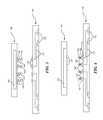
- FIG. 1is a schematic side cross-sectional view of a packaged microdevice in accordance with an embodiment of the invention.
- FIGS. 2A-2Cillustrate stages in a method for packaging a microdevice in accordance with an embodiment of the invention.
- FIG. 2Ais a schematic side cross-sectional view of a substrate with first conductive elements and a die with second conductive elements at one stage of a method for packaging microdevices in accordance with the invention.
- FIG. 2Bis a schematic side cross-sectional view in which the die is inverted such that the first conductive elements are aligned with the second conductive elements.
- FIG. 2Cis a schematic side cross-sectional view of the substrate and the die after connecting the first conductive elements to the second conductive elements.
- FIG. 3is a schematic side cross-sectional view illustrating a stage in another embodiment of a method for packaging microdevices in accordance with the invention.
- FIG. 4is a schematic side cross-sectional view illustrating a stage in still another embodiment of a method for packaging microdevices in accordance with the invention.
- a packaged microdevicecomprises a substrate having a mounting area, contacts in the mounting area, and external connectors electrically coupled to corresponding contacts.
- the microdevicealso includes a die located across from the mounting area and spaced apart from the substrate by a gap.
- the diehas an integrated circuit and pads electrically coupled to the integrated circuit.
- the microdevicefurther includes first and second conductive elements in the gap that form interconnects between the contacts of the substrate and corresponding pads of the die.
- the first conductive elementsare electrically connected to contacts on the substrate, and the second conductive elements are electrically coupled to corresponding pads of the die.
- the first conductive elementsare attached to the second conductive elements at corresponding interfaces such that the interconnects connect the contacts of the substrate directly to corresponding pads on the die within the gap.
- the first conductive elementscomprise first gold bumps deposited onto the contacts of the substrate, and the second conductive elements comprise second gold bumps deposited onto the pads of the die.
- the interfacescan comprise ultrasonic joints or other fixed joints (e.g., welds) between corresponding first and second gold bumps.
- the substratecan further comprise an organic dielectric material and conductive traces electrically coupling the contacts to corresponding external connectors.
- the pads on the dieare juxtaposed to corresponding contacts on the substrate and the first gold bumps are superimposed with corresponding second gold bumps such that the interconnects couple the pads to the contacts without a redistribution structure on the die between the pads and the contacts.
- a packaged microelectronic devicecomprises a substrate having a mounting area, contacts in the mounting area, and external connectors electrically coupled to the contacts.
- the packaged devicecan further include a die located across from the mounting area and spaced apart from the substrate by a gap.
- the diehas pads and an integrated circuit electrically coupled to the pads.
- the packaged devicefurther includes gold interconnects in the gap between the substrate and the die. The individual interconnects have a first cross-sectional dimension at the contacts and a length between the contacts and the die that is greater than the cross-sectional dimension.
- Another aspect of the inventionis directed towards methods for packaging a microelectronic device.
- One embodiment of such a methodincludes arranging a plurality of first gold elements in a pattern corresponding to a pattern of contacts on a substrate, and attaching the first gold elements to corresponding second gold elements.
- the individual pairs of first and second gold elementsform individual interconnects.
- the first gold elementsare attached to contacts of the substrate, and the second gold elements are attached to corresponding pads of a microelectronic die.
- the first gold elementsare arranged in the pattern corresponding to the pattern of contacts on the substrate by depositing first gold bumps onto the contacts of the substrate.
- the second gold elementscomprise second gold bumps, and the method further comprises depositing the second gold bumps onto the pads of the dies.
- the methodcan further comprise attaching the first gold bumps to corresponding second gold bumps after the second gold bumps have been deposited onto the pads.
- the first gold elementsare arranged in the pattern corresponding to the pattern of contacts on the substrate by forming first gold bumps on the contacts of the substrate.
- the first gold elementscan be attached to corresponding second gold elements by depositing second gold bumps onto the first gold bumps, and then the method can further comprise attaching the second gold bumps to corresponding pads of the die after attaching the first gold bumps to the second gold bumps.
- the second gold bumpsare deposited onto the pads of the die before attaching the first gold bumps to the second gold bumps, and then the first gold bumps are then attached to the second gold bumps.
- the contacts of the substrateare attached to the first gold bumps after the first gold bumps have been attached to the second gold bumps.
- Another embodiment of a method of packaging a microelectronic devicecomprises forming a plurality of first gold elements on contacts of a substrate, and forming a plurality of second gold elements in electrical connection with pads of a microelectronic die. The method further includes aligning the first gold elements with corresponding second gold elements, and attaching the first gold elements to the second gold elements to form electrical interconnects between the substrate and the die.
- Still another embodiment of a method of packaging a microelectronic devicecomprises providing a substrate having an organic dielectric material, contacts arranged in an array in a mounting area, and external connectors electrically coupled to the contacts.
- the methodfurther includes providing a microelectronic die having pads arranged in an array corresponding to the contact array and an integrated circuit electrically coupled to the pads.
- the methodfurther includes attaching a plurality of the first gold elements to a plurality of second gold elements, attaching the first gold elements to corresponding contacts, and attaching the second gold elements to corresponding pads.
- the individual pairs of first and second gold elementscomprise individual interconnects between the substrate and the die.
- microelectronic deviceswith a single microelectronic die attached to a substrate.
- the microelectronic devicescan have two or more stacked microelectronic dies electrically coupled to a substrate.
- the microelectronic devicescan be processors, memory devices (DRAM, SDRAM, flash, etc.), imagers, sensors, filters (SAW filters) or other types of devices that require an electrical connection between the dies and a substrate.
- FIG. 1is a schematic side cross-sectional view of a packaged microelectronic device 100 in accordance with an embodiment of the invention.
- the packaged device 100includes a substrate 110 , a die 120 spaced apart from the substrate 110 by a gap 130 , and a plurality of interconnects 140 electrically coupling the die 120 to the substrate 110 .
- the individual interconnects 140can include a first conductive element 142 electrically coupled to the substrate 110 and a second conductive element 144 electrically coupled to the die 120 .
- the first and second conductive elements 142 and 144are separate components that are attached to each other at interfaces 146 .
- the first and second conductive elements 142 and 144can be gold bumps or other small conductive elements that can fit in the gap 130 between the substrate 110 and the die 120 to electrically connect the die 120 directly to the substrate 110 without a redistribution structure on the die 120 .
- the first and second conductive elements 142 and 144also combine to have a standoff height or length that mitigates the need to have (a) highly uniform bump heights and (b) parallelism between the substrate 110 and the die 120 . Therefore, as explained in more detail below, the features and advantages of the interconnects 140 enable gold-to-gold interconnects or other small interconnects to be used in a wide range of applications that are currently limited to solder-based interconnects.
- the substrate 110includes a dielectric material 111 having a die surface 112 with a mounting area 113 and an external surface 114 .
- the substrate 110further includes a plurality of contacts 115 in the mounting area 113 , external connectors 116 at the external surface 114 , and electrical traces 117 between the contacts 115 and corresponding external connectors 116 .
- the dielectric material 111can be an organic material, a ceramic material, or another suitable dielectric material. In many applications, the traces 117 are copper lines on layers of an organic dielectric material 111 that are laminated together.
- the die 120can be a semiconductor die or other type of microelectronic die. In many applications, the die 120 has an integrated circuit 122 and a plurality of pads 124 electrically coupled to the integrated circuit 122 .
- the pads 124can be external bond-pads as shown in FIG. 1 , or the pads 120 can be embedded in the die 120 and connected to the interconnects 140 by through-wafer interconnects.
- the die 120can be a processor, a memory device, an imager, a sensor, a filter, or other type of microelectronic device. Suitable memory devices, for example, include DRAM and flash memory devices.
- the contacts 115are arranged in a contact array, and the pads 124 are arranged in a pad array that mirrors the contact array.
- the die 120is positioned relative to the substrate 110 such that individual pads 124 are aligned with corresponding individual contacts 115 across the gap 130 .
- the pads 124are accordingly juxtaposed or otherwise superimposed relative to corresponding contacts 115 .
- the contact arraymay be a universal array with a large number of contacts such that the array of pads 124 is juxtaposed to only a subset of the contacts 115 on the substrate 110 .
- the first conductive elements 142are electrically connected to the contacts 115 of the substrate 110 , and the second conductive elements 144 are electrically coupled to corresponding pads 124 of the die 120 .
- Individual first conductive elements 142are attached to corresponding individual second conductive elements 144 at interfaces 146 such that individual pairs of first and second conductive elements 142 and 144 form the direct interconnects 140 in the gap 130 between the contacts 115 and corresponding pads 124 .
- the multi-bump interconnects 140electrically couple the pads 124 to the contacts 115 without constructing a redistribution layer on the die 120 .
- the first conductive elements 142can be gold bumps, and the second conductive elements 144 can be gold bumps formed separately from the first gold bumps 144 .
- the first conductive elements 142 and second elements 144can be attached at the interfaces 146 such that the interconnects 140 have a length “L” between the contacts 115 and corresponding pads 124 that is greater than a cross-sectional dimension “W” at the contacts 115 and/or the pads 124 .
- the packaged microdevice 100can further include an optional resist layer 150 (shown in broken lines) on the die surface 112 of the substrate 110 with an opening (not shown) in which the contacts are located.
- the packaged device 100can further include an optional casing 160 molded around the die 120 to protect the die 120 from external hazards.
- the packaged device 100can further include an under fill material in the gap 130 to protect the interconnects 140 when the casing 160 is molded around the die 120 .
- FIGS. 2A-2Care schematic side cross-sectional views illustrating different stages of a method for fabricating the packaged microdevice 100 in accordance with an embodiment of the invention.
- this embodiment of the methodincludes depositing the first conductive elements 142 onto the contacts 115 and depositing the second conductive elements 144 onto the pads 124 .
- the first and second conductive elements 142 and 144are accordingly separate components in this embodiment such that the first conductive elements 142 are attached to the contacts 115 and the second conductive elements 144 are attached to the pads 124 before the first and second conductive elements 142 and 144 are connected to each other.
- the first conductive elements 142can be first gold stud bumps and the second conductive elements 144 can be second gold stud bumps.
- the first and second gold stud bumpsare formed using a wire bonding machine by forming a gold sphere at the tip of the wire, attaching the sphere to the contact 115 or pad 124 , and severing the sphere from the wire. This stage of the method further includes flipping the die 120 (arrow F) to invert the die 120 over the substrate 110 for further processing. In an alternative embodiment, the substrate 110 can be flipped to be inverted over the die 120 .
- FIG. 2Billustrates a stage after which the die 120 has been flipped to be inverted over the substrate 110 .
- the methodincludes aligning the pads 124 with corresponding contacts 115 such that the first conductive elements 142 face corresponding second conductive elements 144 .
- the methodcontinues by moving die 120 and/or the substrate 110 toward each other until the first conductive elements 142 contact corresponding second conductive elements 144 .
- FIG. 2Cillustrates a stage at which the first conductive elements 142 contact corresponding second conductive elements 144 .
- the methodcontinues by applying a down force (arrow D) to the die 120 while transmitting an energy (arrow E) to the first and second conductive elements 142 and 144 .
- the down force and energyform a fixed joint at the interfaces 146 between the first conductive elements 142 and corresponding second conductive elements 144 .
- the energycan be ultrasonic energy or heat such that the interface 146 is a diffusion joint between the first conductive elements 142 and corresponding second conductive elements 144 .
- Individual pairs of first and second conductive elements 142 and 144accordingly form direct interconnects between the contacts 115 and the pads 124 .
- an under fill materialmay be placed in the gap 130 and a casing may be molded over the die 120 to further protect the die 120 .
- the multi-bump interconnects 140 with two or more stacked bumpsprovide a standoff height between the substrate 110 and the die 120 . This can compensate for non-uniformities in the height/lengths of the interconnects and/or a lack of parallelism between the die 120 and the substrate 110 .
- the larger standoff heightaccordingly enables laminates and other types of non-ceramic substrates to be used with gold-to-gold interconnects or other types of small interconnects in flip-chip applications.
- the advantages of using a gold interconnect or other type of small, lead-free interconnect for environmental purposescan be realized in applications that use laminated substrates and/or high density arrays with high pin counts.
- the first and second conductive elements 142 and 144can be formed of gold balls or other small, conductive stud bumps that are much smaller than solder balls. This enables flip-chip interconnection between very fine pitched bond-pad arrays on a die and corresponding contact arrays on a substrate without having to use a redistribution layer. It will be appreciated that redistribution layers have dielectric layers, conductive traces and additional pads to effectively increase the spacing between the pads to a larger array on the die. The direct connection provided by the interconnects 140 , however, eliminates the need to effectively space the pads apart by a greater distance. As such, several embodiments of the packaged device 100 eliminate the costs and time for manufacturing redistribution layers on wafers.
- Still another advantage of several embodiments of the packaged device 100 illustrated in FIG. 1is that the design of the dies is not restricted to bond-pad arrangements that can be wire bonded or need a redistribution layer to be coupled to the substrate. This enables higher pin counts and/or smaller packages. As a result, high performance devices can have relatively small packages for use in cell phones, PDAs, portable computers and other products where space is a premium.
- first conductive elements 142are attached to the second conductive elements 144 only after the first conductive elements have been deposited onto the contacts 115 and the second conductive elements 144 have been deposited onto the pads 124 is expected to provide better diffusion bonding between the first and second conductive elements 142 and 144 . More specifically, the down force used to connect the conductive elements together (see FIG. 2C ) can be less because the slip interface between the first and second conductive elements 142 and 144 forms a stronger diffusion joint when the first and second conductive elements 142 and 144 are first attached to the substrate 110 and the die 120 , respectively. This is expected to reduce or otherwise mitigate damage caused to the die 120 during the attaching stage illustrated in FIG. 2C .
- FIG. 3is a schematic side cross-sectional view illustrating a die 120 being attached to a substrate 110 to form a packaged device in accordance with another method of the invention.
- the second conductive elements 144are deposited onto the pads 124 of the die 120 , and then the first conductive elements 142 are attached to the second conductive elements 144 to form multi-bump interconnects 140 on the die 120 .
- the die 120is then inverted as shown in FIG. 3 to align the interconnects 140 with corresponding contacts 115 of the substrate.
- the first conductive elements 142are then attached to corresponding contacts 115 of the substrate 110 by applying a down force and an appropriate energy to the interconnects 140 .
- FIG. 4is a schematic side cross-sectional view illustrating a stage in forming a packaged device in accordance with another method of the invention.
- the first conductive elements 142are deposited onto the contacts 115 and then the second conductive elements 144 are attached to the first conductive elements 142 to form multi-bump interconnects 140 on the substrate 110 .
- the die 120is then positioned such that the pads 124 are aligned with corresponding multi-bump interconnects 140 .
- the substrate 110 and/or the die 120are then moved toward each other until the second conductive elements 144 contact corresponding pads 124 of the die 120 .
- the appropriate down force and energyare then applied to the interconnects to attach the second conductive elements 144 to corresponding pads 124 .
- the illustrated interconnectshave two separate conductive elements, but in other embodiments, the individual interconnects can have three or more conductive elements.
- the flip-chip interconnectscan be used between stacked dies in a stacked die arrangement. Accordingly, the invention is not limited except as by the appended claims.
Landscapes
- Engineering & Computer Science (AREA)
- Microelectronics & Electronic Packaging (AREA)
- Computer Hardware Design (AREA)
- Power Engineering (AREA)
- Physics & Mathematics (AREA)
- Condensed Matter Physics & Semiconductors (AREA)
- General Physics & Mathematics (AREA)
- Manufacturing & Machinery (AREA)
- Wire Bonding (AREA)
Abstract
Description
- This application is a divisional of U.S. application Ser. No. 11/509,990 filed Aug. 25, 2006, now U.S. Pat. No. 7,868,440, which is incorporated herein by reference in its entirety.
- The present invention is related to microdevices and methods for packaging microdevices using gold-to-gold interconnects or other types of conductive elements in high-density contact arrays.
- Microelectronic devices generally have a die (i.e., a chip) that includes integrated circuitry having a high density of very small components. In a typical process, a large number of dies are manufactured on a single wafer using many different processes that may be repeated at various stages (e.g., implanting, doping, photolithography, chemical vapor deposition, plasma vapor deposition, plating, planarizing, etching, etc.). The dies typically include an array of very small bond-pads electrically coupled to the integrated circuitry. The bond-pads are the external electrical contacts on the die through which the supply voltage, signals, etc., are transmitted to and from the integrated circuitry. The dies are then separated from one another (i.e., singulated) by dicing the wafer and backgrinding the individual dies. After the dies have been singulated, they are typically “packaged” to couple the bond-pads to a larger array of electrical terminals that can be more easily coupled to the various power supply lines, signal lines, and ground lines.
- Electronic products require packaged microelectronic devices to have an extremely high density of components in very limited space. For example, the space available for memory devices, processors, displays, and other microelectronic components is quite limited in cellphones, PDAs, portable computers, storage devices, media players and many other products. As such, there is a strong drive to reduce the surface area or “footprint” of a microelectronic device on a printed circuit board, lead frame, or other type of substrate. Reducing the size of a microelectronic device is difficult because high performance microelectronic dies generally have more bond-pads that result in larger ball-grid arrays and thus larger footprints.
- “Flip-chip” packages are attractive for such high performance, small microelectronic devices. These devices are referred to as “flip-chips” because they are typically manufactured on a wafer and have an active side with bond-pads that initially face upward. After completing the die, it is singulated and inverted or “flipped” such that the active side bearing the bond-pads faces downward for attachment to a substrate. The bond-pads are usually coupled to terminals, such as conductive “bumps,” that electrically and mechanically connect the die to the substrate. The bumps on the flip-chip are generally formed from solder, conductive polymers, or other materials. When the bumps are made from solder, they are reflowed to form discrete solder joints between the flip-chip component and the substrate. This leaves a small gap between the die and the substrate. To enhance the integrity of the joint between the die and the substrate, an underfill material is generally introduced into the gap. The underfill material bears some of the stress placed on the components and protects the components from moisture, chemicals, and other contaminants. The underfill material can include filler particles to increase the rigidity of the material and modify the coefficient of thermal expansion of the material.
- Most flip-chip devices use a lead-tin solder that requires flux to remove oxide during assembly. Although lead-tin solders provide high yields and reliable connections, soldering generally involves potentially hazardous materials and presents other challenges. First, it is generally costly and inefficient to handle hazardous materials. Second, the temperatures of reflow processes may be above the upper limits for some of the materials used in the packages. Third, solder interconnects are relatively large compared to gold-to-gold interconnects. Many solder-based flip-chip packages accordingly require a redistribution layer on the die that redistributes the very fine pitch of the bond-pads to an array having a larger pitch to accommodate the solder interconnects.
- Gold-to-gold interconnects are one alternative to solder interconnects. Gold-to-gold interconnects generally have gold stud bumps placed on the die bond-pads through a modification of the “ball bonding” process used in conventional wire-bonding. In ball bonding, the tip of the gold bond wire is melted to form a sphere, and the bonding tool presses this sphere against a bond-pad while applying mechanical force, heat and ultrasonic energy to create a metallic connection. The gold is broken just above the ball to form a gold ball or “gold stud bump” on the bond-pad. After placing the gold stud bumps on a chip, they may be flattened by mechanical pressure to provide a flat-top surface and uniform bump height (i.e., co-planarity). Gold stud bumps are relatively easy to form with conventional wire-bonding equipment, and they do not use hazardous materials that require expensive and sophisticated handling processes. Gold stud bumps can also be quite small, and are thus very useful for fine pitch arrays with a large number of very small bond-pads.
- Gold stud bumps, however, have only been used in limited applications because it is challenging to use them in many types of packaged devices. For example, because gold stud bumps are quite small, they must have good co-planarity and there must be good parallelism between the die and substrate to obtain good diffusion bonding. Misalignment between the die and the substrate, or non-uniform bump heights, may cause openings in the interconnects. As a result, gold stud bumps are not used in high density arrays on laminate substrates formed from organic dielectric materials. Additionally, large arrays require more ultrasonic power and greater down forces to attach the gold stud bumps to the bond-pads, and this can damage the dies. Therefore, it would be desirable to develop a packaged device and a method for packaging devices in which gold stud bumps can be formed in large arrays on organic substrates or other types of substrates to enable gold interconnects to be used in a wider range of applications.
FIG. 1 is a schematic side cross-sectional view of a packaged microdevice in accordance with an embodiment of the invention.FIGS. 2A-2C illustrate stages in a method for packaging a microdevice in accordance with an embodiment of the invention.FIG. 2A is a schematic side cross-sectional view of a substrate with first conductive elements and a die with second conductive elements at one stage of a method for packaging microdevices in accordance with the invention.FIG. 2B is a schematic side cross-sectional view in which the die is inverted such that the first conductive elements are aligned with the second conductive elements.FIG. 2C is a schematic side cross-sectional view of the substrate and the die after connecting the first conductive elements to the second conductive elements.FIG. 3 is a schematic side cross-sectional view illustrating a stage in another embodiment of a method for packaging microdevices in accordance with the invention.FIG. 4 is a schematic side cross-sectional view illustrating a stage in still another embodiment of a method for packaging microdevices in accordance with the invention.- The following disclosure describes several embodiments of microdevices and methods for packaging microdevices. One embodiment of a packaged microdevice comprises a substrate having a mounting area, contacts in the mounting area, and external connectors electrically coupled to corresponding contacts. The microdevice also includes a die located across from the mounting area and spaced apart from the substrate by a gap. The die has an integrated circuit and pads electrically coupled to the integrated circuit. The microdevice further includes first and second conductive elements in the gap that form interconnects between the contacts of the substrate and corresponding pads of the die. The first conductive elements are electrically connected to contacts on the substrate, and the second conductive elements are electrically coupled to corresponding pads of the die. The first conductive elements are attached to the second conductive elements at corresponding interfaces such that the interconnects connect the contacts of the substrate directly to corresponding pads on the die within the gap.
- In several embodiments, the first conductive elements comprise first gold bumps deposited onto the contacts of the substrate, and the second conductive elements comprise second gold bumps deposited onto the pads of the die. The interfaces can comprise ultrasonic joints or other fixed joints (e.g., welds) between corresponding first and second gold bumps. In additional embodiments, the substrate can further comprise an organic dielectric material and conductive traces electrically coupling the contacts to corresponding external connectors. In many embodiments, the pads on the die are juxtaposed to corresponding contacts on the substrate and the first gold bumps are superimposed with corresponding second gold bumps such that the interconnects couple the pads to the contacts without a redistribution structure on the die between the pads and the contacts.
- In another embodiment, a packaged microelectronic device comprises a substrate having a mounting area, contacts in the mounting area, and external connectors electrically coupled to the contacts. The packaged device can further include a die located across from the mounting area and spaced apart from the substrate by a gap. The die has pads and an integrated circuit electrically coupled to the pads. The packaged device further includes gold interconnects in the gap between the substrate and the die. The individual interconnects have a first cross-sectional dimension at the contacts and a length between the contacts and the die that is greater than the cross-sectional dimension.
- Another aspect of the invention is directed towards methods for packaging a microelectronic device. One embodiment of such a method includes arranging a plurality of first gold elements in a pattern corresponding to a pattern of contacts on a substrate, and attaching the first gold elements to corresponding second gold elements. The individual pairs of first and second gold elements form individual interconnects. Additionally, the first gold elements are attached to contacts of the substrate, and the second gold elements are attached to corresponding pads of a microelectronic die.
- In one specific example, the first gold elements are arranged in the pattern corresponding to the pattern of contacts on the substrate by depositing first gold bumps onto the contacts of the substrate. In this embodiment, the second gold elements comprise second gold bumps, and the method further comprises depositing the second gold bumps onto the pads of the dies. The method can further comprise attaching the first gold bumps to corresponding second gold bumps after the second gold bumps have been deposited onto the pads.
- In a different embodiment, the first gold elements are arranged in the pattern corresponding to the pattern of contacts on the substrate by forming first gold bumps on the contacts of the substrate. The first gold elements can be attached to corresponding second gold elements by depositing second gold bumps onto the first gold bumps, and then the method can further comprise attaching the second gold bumps to corresponding pads of the die after attaching the first gold bumps to the second gold bumps.
- In an alternative embodiment, the second gold bumps are deposited onto the pads of the die before attaching the first gold bumps to the second gold bumps, and then the first gold bumps are then attached to the second gold bumps. The contacts of the substrate are attached to the first gold bumps after the first gold bumps have been attached to the second gold bumps.
- Another embodiment of a method of packaging a microelectronic device comprises forming a plurality of first gold elements on contacts of a substrate, and forming a plurality of second gold elements in electrical connection with pads of a microelectronic die. The method further includes aligning the first gold elements with corresponding second gold elements, and attaching the first gold elements to the second gold elements to form electrical interconnects between the substrate and the die.
- Still another embodiment of a method of packaging a microelectronic device comprises providing a substrate having an organic dielectric material, contacts arranged in an array in a mounting area, and external connectors electrically coupled to the contacts. The method further includes providing a microelectronic die having pads arranged in an array corresponding to the contact array and an integrated circuit electrically coupled to the pads. The method further includes attaching a plurality of the first gold elements to a plurality of second gold elements, attaching the first gold elements to corresponding contacts, and attaching the second gold elements to corresponding pads. The individual pairs of first and second gold elements comprise individual interconnects between the substrate and the die.
- Specific details of several embodiments of the invention are described below with reference microelectronic devices with a single microelectronic die attached to a substrate. However, in other embodiments, the microelectronic devices can have two or more stacked microelectronic dies electrically coupled to a substrate. The microelectronic devices can be processors, memory devices (DRAM, SDRAM, flash, etc.), imagers, sensors, filters (SAW filters) or other types of devices that require an electrical connection between the dies and a substrate. Several details describing well-known structures or processes often associated with fabricating microelectronic dies and devices are not described herein for purposes of brevity. Also, several of the embodiments of the invention can have different configurations, components, or procedures than those described in this section. A person of ordinary skill in the art, therefore, will accordingly understand that the invention may have other embodiments with additional elements, or that the invention may have other embodiments without several of the elements and features shown and described below with reference to
FIGS. 1-4 . FIG. 1 is a schematic side cross-sectional view of a packagedmicroelectronic device 100 in accordance with an embodiment of the invention. In this embodiment, the packageddevice 100 includes asubstrate 110, adie 120 spaced apart from thesubstrate 110 by agap 130, and a plurality ofinterconnects 140 electrically coupling thedie 120 to thesubstrate 110. Theindividual interconnects 140 can include a firstconductive element 142 electrically coupled to thesubstrate 110 and a secondconductive element 144 electrically coupled to thedie 120. As explained in more detail below, the first and secondconductive elements interfaces 146. The first and secondconductive elements gap 130 between thesubstrate 110 and thedie 120 to electrically connect the die120 directly to thesubstrate 110 without a redistribution structure on thedie 120. The first and secondconductive elements substrate 110 and thedie 120. Therefore, as explained in more detail below, the features and advantages of theinterconnects 140 enable gold-to-gold interconnects or other small interconnects to be used in a wide range of applications that are currently limited to solder-based interconnects.- The
substrate 110 includes adielectric material 111 having adie surface 112 with a mountingarea 113 and anexternal surface 114. Thesubstrate 110 further includes a plurality ofcontacts 115 in the mountingarea 113,external connectors 116 at theexternal surface 114, andelectrical traces 117 between thecontacts 115 and correspondingexternal connectors 116. Thedielectric material 111 can be an organic material, a ceramic material, or another suitable dielectric material. In many applications, thetraces 117 are copper lines on layers of an organicdielectric material 111 that are laminated together. - The die120 can be a semiconductor die or other type of microelectronic die. In many applications, the
die 120 has an integratedcircuit 122 and a plurality ofpads 124 electrically coupled to theintegrated circuit 122. Thepads 124 can be external bond-pads as shown inFIG. 1 , or thepads 120 can be embedded in thedie 120 and connected to theinterconnects 140 by through-wafer interconnects. The die120 can be a processor, a memory device, an imager, a sensor, a filter, or other type of microelectronic device. Suitable memory devices, for example, include DRAM and flash memory devices. - In the embodiment of the packaged
microdevice 100 shown inFIG. 1 , thecontacts 115 are arranged in a contact array, and thepads 124 are arranged in a pad array that mirrors the contact array. Thedie 120 is positioned relative to thesubstrate 110 such thatindividual pads 124 are aligned with correspondingindividual contacts 115 across thegap 130. Thepads 124 are accordingly juxtaposed or otherwise superimposed relative tocorresponding contacts 115. In other embodiments, the contact array may be a universal array with a large number of contacts such that the array ofpads 124 is juxtaposed to only a subset of thecontacts 115 on thesubstrate 110. - The first
conductive elements 142 are electrically connected to thecontacts 115 of thesubstrate 110, and the secondconductive elements 144 are electrically coupled tocorresponding pads 124 of thedie 120. Individual firstconductive elements 142 are attached to corresponding individual secondconductive elements 144 atinterfaces 146 such that individual pairs of first and secondconductive elements direct interconnects 140 in thegap 130 between thecontacts 115 andcorresponding pads 124. As a result, in many embodiments the multi-bump interconnects140 electrically couple thepads 124 to thecontacts 115 without constructing a redistribution layer on thedie 120. The firstconductive elements 142 can be gold bumps, and the secondconductive elements 144 can be gold bumps formed separately from the first gold bumps144. The firstconductive elements 142 andsecond elements 144, moreover, can be attached at theinterfaces 146 such that theinterconnects 140 have a length “L” between thecontacts 115 andcorresponding pads 124 that is greater than a cross-sectional dimension “W” at thecontacts 115 and/or thepads 124. - The packaged
microdevice 100 can further include an optional resist layer150 (shown in broken lines) on thedie surface 112 of thesubstrate 110 with an opening (not shown) in which the contacts are located. The packageddevice 100 can further include anoptional casing 160 molded around thedie 120 to protect the die120 from external hazards. In several embodiments, the packageddevice 100 can further include an under fill material in thegap 130 to protect theinterconnects 140 when thecasing 160 is molded around thedie 120. FIGS. 2A-2C are schematic side cross-sectional views illustrating different stages of a method for fabricating the packagedmicrodevice 100 in accordance with an embodiment of the invention. Like references numbers refer to like components inFIGS. 1-2C . Referring toFIG. 2A , this embodiment of the method includes depositing the firstconductive elements 142 onto thecontacts 115 and depositing the secondconductive elements 144 onto thepads 124. The first and secondconductive elements conductive elements 142 are attached to thecontacts 115 and the secondconductive elements 144 are attached to thepads 124 before the first and secondconductive elements conductive elements 142 can be first gold stud bumps and the secondconductive elements 144 can be second gold stud bumps. In one embodiment, the first and second gold stud bumps are formed using a wire bonding machine by forming a gold sphere at the tip of the wire, attaching the sphere to thecontact 115 orpad 124, and severing the sphere from the wire. This stage of the method further includes flipping the die120 (arrow F) to invert thedie 120 over thesubstrate 110 for further processing. In an alternative embodiment, thesubstrate 110 can be flipped to be inverted over thedie 120.FIG. 2B illustrates a stage after which thedie 120 has been flipped to be inverted over thesubstrate 110. At this stage, the method includes aligning thepads 124 withcorresponding contacts 115 such that the firstconductive elements 142 face corresponding secondconductive elements 144. The method continues by movingdie 120 and/or thesubstrate 110 toward each other until the firstconductive elements 142 contact corresponding secondconductive elements 144.FIG. 2C illustrates a stage at which the firstconductive elements 142 contact corresponding secondconductive elements 144. At this stage, the method continues by applying a down force (arrow D) to the die120 while transmitting an energy (arrow E) to the first and secondconductive elements interfaces 146 between the firstconductive elements 142 and corresponding secondconductive elements 144. The energy can be ultrasonic energy or heat such that theinterface 146 is a diffusion joint between the firstconductive elements 142 and corresponding secondconductive elements 144. Individual pairs of first and secondconductive elements contacts 115 and thepads 124. After connecting thefirst elements 142 to thesecond elements 144, an under fill material may be placed in thegap 130 and a casing may be molded over thedie 120 to further protect thedie 120.- One advantage of several embodiments of the packaged
device 100 is that themulti-bump interconnects 140 with two or more stacked bumps provide a standoff height between thesubstrate 110 and thedie 120. This can compensate for non-uniformities in the height/lengths of the interconnects and/or a lack of parallelism between the die120 and thesubstrate 110. The larger standoff height accordingly enables laminates and other types of non-ceramic substrates to be used with gold-to-gold interconnects or other types of small interconnects in flip-chip applications. As a result, the advantages of using a gold interconnect or other type of small, lead-free interconnect for environmental purposes can be realized in applications that use laminated substrates and/or high density arrays with high pin counts. - Another advantage of several embodiments of the packaged
device 100 illustrated inFIGS. 1-2C is that the first and secondconductive elements interconnects 140, however, eliminates the need to effectively space the pads apart by a greater distance. As such, several embodiments of the packageddevice 100 eliminate the costs and time for manufacturing redistribution layers on wafers. - Still another advantage of several embodiments of the packaged
device 100 illustrated inFIG. 1 is that the design of the dies is not restricted to bond-pad arrangements that can be wire bonded or need a redistribution layer to be coupled to the substrate. This enables higher pin counts and/or smaller packages. As a result, high performance devices can have relatively small packages for use in cell phones, PDAs, portable computers and other products where space is a premium. - The specific embodiment in which the first
conductive elements 142 are attached to the secondconductive elements 144 only after the first conductive elements have been deposited onto thecontacts 115 and the secondconductive elements 144 have been deposited onto thepads 124 is expected to provide better diffusion bonding between the first and secondconductive elements FIG. 2C ) can be less because the slip interface between the first and secondconductive elements conductive elements substrate 110 and thedie 120, respectively. This is expected to reduce or otherwise mitigate damage caused to thedie 120 during the attaching stage illustrated inFIG. 2C . FIG. 3 is a schematic side cross-sectional view illustrating adie 120 being attached to asubstrate 110 to form a packaged device in accordance with another method of the invention. Like reference numbers refer to like components inFIGS. 1-3 . In the embodiment illustrated inFIG. 3 , the secondconductive elements 144 are deposited onto thepads 124 of thedie 120, and then the firstconductive elements 142 are attached to the secondconductive elements 144 to formmulti-bump interconnects 140 on thedie 120. Thedie 120 is then inverted as shown inFIG. 3 to align theinterconnects 140 withcorresponding contacts 115 of the substrate. The firstconductive elements 142 are then attached to correspondingcontacts 115 of thesubstrate 110 by applying a down force and an appropriate energy to theinterconnects 140.FIG. 4 is a schematic side cross-sectional view illustrating a stage in forming a packaged device in accordance with another method of the invention. In this embodiment, the firstconductive elements 142 are deposited onto thecontacts 115 and then the secondconductive elements 144 are attached to the firstconductive elements 142 to formmulti-bump interconnects 140 on thesubstrate 110. Thedie 120 is then positioned such that thepads 124 are aligned with corresponding multi-bump interconnects140. Thesubstrate 110 and/or thedie 120 are then moved toward each other until the secondconductive elements 144contact corresponding pads 124 of thedie 120. The appropriate down force and energy are then applied to the interconnects to attach the secondconductive elements 144 tocorresponding pads 124.- From the foregoing, it will be appreciated that specific embodiments of the invention have been described herein for purposes of illustration, but that various modifications may be made without deviating from the spirit and scope of the invention. For example, the illustrated interconnects have two separate conductive elements, but in other embodiments, the individual interconnects can have three or more conductive elements. Additionally, the flip-chip interconnects can be used between stacked dies in a stacked die arrangement. Accordingly, the invention is not limited except as by the appended claims.
Claims (21)
Priority Applications (2)
| Application Number | Priority Date | Filing Date | Title |
|---|---|---|---|
| US12/987,890US8354301B2 (en) | 2006-08-25 | 2011-01-10 | Packaged microdevices and methods for manufacturing packaged microdevices |
| US13/741,789US8987885B2 (en) | 2006-08-25 | 2013-01-15 | Packaged microdevices and methods for manufacturing packaged microdevices |
Applications Claiming Priority (2)
| Application Number | Priority Date | Filing Date | Title |
|---|---|---|---|
| US11/509,990US7868440B2 (en) | 2006-08-25 | 2006-08-25 | Packaged microdevices and methods for manufacturing packaged microdevices |
| US12/987,890US8354301B2 (en) | 2006-08-25 | 2011-01-10 | Packaged microdevices and methods for manufacturing packaged microdevices |
Related Parent Applications (1)
| Application Number | Title | Priority Date | Filing Date |
|---|---|---|---|
| US11/509,990DivisionUS7868440B2 (en) | 2006-08-25 | 2006-08-25 | Packaged microdevices and methods for manufacturing packaged microdevices |
Related Child Applications (1)
| Application Number | Title | Priority Date | Filing Date |
|---|---|---|---|
| US13/741,789ContinuationUS8987885B2 (en) | 2006-08-25 | 2013-01-15 | Packaged microdevices and methods for manufacturing packaged microdevices |
Publications (2)
| Publication Number | Publication Date |
|---|---|
| US20110104857A1true US20110104857A1 (en) | 2011-05-05 |
| US8354301B2 US8354301B2 (en) | 2013-01-15 |
Family
ID=39112596
Family Applications (3)
| Application Number | Title | Priority Date | Filing Date |
|---|---|---|---|
| US11/509,990Active2026-10-10US7868440B2 (en) | 2006-08-25 | 2006-08-25 | Packaged microdevices and methods for manufacturing packaged microdevices |
| US12/987,890ActiveUS8354301B2 (en) | 2006-08-25 | 2011-01-10 | Packaged microdevices and methods for manufacturing packaged microdevices |
| US13/741,789ActiveUS8987885B2 (en) | 2006-08-25 | 2013-01-15 | Packaged microdevices and methods for manufacturing packaged microdevices |
Family Applications Before (1)
| Application Number | Title | Priority Date | Filing Date |
|---|---|---|---|
| US11/509,990Active2026-10-10US7868440B2 (en) | 2006-08-25 | 2006-08-25 | Packaged microdevices and methods for manufacturing packaged microdevices |
Family Applications After (1)
| Application Number | Title | Priority Date | Filing Date |
|---|---|---|---|
| US13/741,789ActiveUS8987885B2 (en) | 2006-08-25 | 2013-01-15 | Packaged microdevices and methods for manufacturing packaged microdevices |
Country Status (1)
| Country | Link |
|---|---|
| US (3) | US7868440B2 (en) |
Cited By (1)
| Publication number | Priority date | Publication date | Assignee | Title |
|---|---|---|---|---|
| US10923365B2 (en)* | 2018-10-28 | 2021-02-16 | Richwave Technology Corp. | Connection structure and method for forming the same |
Families Citing this family (18)
| Publication number | Priority date | Publication date | Assignee | Title |
|---|---|---|---|---|
| US8143108B2 (en) | 2004-10-07 | 2012-03-27 | Stats Chippac, Ltd. | Semiconductor device and method of dissipating heat from thin package-on-package mounted to substrate |
| USRE44438E1 (en) | 2001-02-27 | 2013-08-13 | Stats Chippac, Ltd. | Semiconductor device and method of dissipating heat from thin package-on-package mounted to substrate |
| US20020121707A1 (en)* | 2001-02-27 | 2002-09-05 | Chippac, Inc. | Super-thin high speed flip chip package |
| US7868440B2 (en)* | 2006-08-25 | 2011-01-11 | Micron Technology, Inc. | Packaged microdevices and methods for manufacturing packaged microdevices |
| US9064781B2 (en)* | 2011-03-03 | 2015-06-23 | Broadcom Corporation | Package 3D interconnection and method of making same |
| US8508045B2 (en) | 2011-03-03 | 2013-08-13 | Broadcom Corporation | Package 3D interconnection and method of making same |
| KR101932727B1 (en)* | 2012-05-07 | 2018-12-27 | 삼성전자주식회사 | Bump structure, semiconductor package having the bump structure, and method of manufacturing the bump structure |
| US9385006B2 (en)* | 2012-06-21 | 2016-07-05 | STATS ChipPAC Pte. Ltd. | Semiconductor device and method of forming an embedded SOP fan-out package |
| US9117873B2 (en)* | 2012-09-27 | 2015-08-25 | Apple Inc. | Direct multiple substrate die assembly |
| KR20140119522A (en)* | 2013-04-01 | 2014-10-10 | 삼성전자주식회사 | Semiconductor package having package on package structure |
| US10083932B2 (en)* | 2014-01-17 | 2018-09-25 | Nvidia Corporation | Package on package arrangement and method |
| US9620436B2 (en)* | 2014-04-09 | 2017-04-11 | Invensas Corporation | Light emitting diode device with reconstituted LED components on substrate |
| US9875997B2 (en)* | 2014-12-16 | 2018-01-23 | Qualcomm Incorporated | Low profile reinforced package-on-package semiconductor device |
| US9397074B1 (en) | 2015-04-29 | 2016-07-19 | Advanced Semiconductor Engineering, Inc. | Semiconductor device package and method of manufacturing the same |
| CN207781947U (en)* | 2017-03-10 | 2018-08-28 | 唐虞企业股份有限公司 | Connector with a locking member |
| TWI770440B (en)* | 2018-12-07 | 2022-07-11 | 美商艾馬克科技公司 | Semiconductor package and fabricating method thereof |
| CN111029267B (en)* | 2019-11-22 | 2021-12-24 | 中国电子科技集团公司第十三研究所 | Flip interconnection structure and preparation method thereof |
| US11133259B2 (en)* | 2019-12-12 | 2021-09-28 | International Business Machines Corporation | Multi-chip package structure having high density chip interconnect bridge with embedded power distribution network |
Citations (84)
| Publication number | Priority date | Publication date | Assignee | Title |
|---|---|---|---|---|
| US5128831A (en)* | 1991-10-31 | 1992-07-07 | Micron Technology, Inc. | High-density electronic package comprising stacked sub-modules which are electrically interconnected by solder-filled vias |
| US5180093A (en)* | 1991-09-05 | 1993-01-19 | Cray Research, Inc. | Apparatus for ultrasonic bonding |
| US5252857A (en)* | 1991-08-05 | 1993-10-12 | International Business Machines Corporation | Stacked DCA memory chips |
| US5518957A (en)* | 1991-10-10 | 1996-05-21 | Samsung Electronics Co., Ltd. | Method for making a thin profile semiconductor package |
| US5677566A (en)* | 1995-05-08 | 1997-10-14 | Micron Technology, Inc. | Semiconductor chip package |
| US5851845A (en)* | 1995-12-18 | 1998-12-22 | Micron Technology, Inc. | Process for packaging a semiconductor die using dicing and testing |
| US5883426A (en)* | 1996-04-18 | 1999-03-16 | Nec Corporation | Stack module |
| US5891753A (en)* | 1997-01-24 | 1999-04-06 | Micron Technology, Inc. | Method and apparatus for packaging flip chip bare die on printed circuit boards |
| US5925930A (en)* | 1996-05-21 | 1999-07-20 | Micron Technology, Inc. | IC contacts with palladium layer and flexible conductive epoxy bumps |
| US5933713A (en)* | 1998-04-06 | 1999-08-03 | Micron Technology, Inc. | Method of forming overmolded chip scale package and resulting product |
| US5946553A (en)* | 1991-06-04 | 1999-08-31 | Micron Technology, Inc. | Process for manufacturing a semiconductor package with bi-substrate die |
| US5952716A (en)* | 1997-04-16 | 1999-09-14 | International Business Machines Corporation | Pin attach structure for an electronic package |
| US5986209A (en)* | 1997-07-09 | 1999-11-16 | Micron Technology, Inc. | Package stack via bottom leaded plastic (BLP) packaging |
| US5990566A (en)* | 1998-05-20 | 1999-11-23 | Micron Technology, Inc. | High density semiconductor package |
| US6004867A (en)* | 1996-12-16 | 1999-12-21 | Samsung Electronics Co., Ltd. | Chip-size packages assembled using mass production techniques at the wafer-level |
| US6008070A (en)* | 1998-05-21 | 1999-12-28 | Micron Technology, Inc. | Wafer level fabrication and assembly of chip scale packages |
| US6020629A (en)* | 1998-06-05 | 2000-02-01 | Micron Technology, Inc. | Stacked semiconductor package and method of fabrication |
| US6022757A (en)* | 1997-03-28 | 2000-02-08 | Sanyo Electric Co., Ltd. | Semiconductor device and manufacturing method |
| US6025648A (en)* | 1997-04-17 | 2000-02-15 | Nec Corporation | Shock resistant semiconductor device and method for producing same |
| US6028365A (en)* | 1998-03-30 | 2000-02-22 | Micron Technology, Inc. | Integrated circuit package and method of fabrication |
| US6048755A (en)* | 1998-11-12 | 2000-04-11 | Micron Technology, Inc. | Method for fabricating BGA package using substrate with patterned solder mask open in die attach area |
| US6051878A (en)* | 1997-03-10 | 2000-04-18 | Micron Technology, Inc. | Method of constructing stacked packages |
| US6072233A (en)* | 1998-05-04 | 2000-06-06 | Micron Technology, Inc. | Stackable ball grid array package |
| US6072236A (en)* | 1996-03-07 | 2000-06-06 | Micron Technology, Inc. | Micromachined chip scale package |
| US6081429A (en)* | 1999-01-20 | 2000-06-27 | Micron Technology, Inc. | Test interposer for use with ball grid array packages assemblies and ball grid array packages including same and methods |
| US6089920A (en)* | 1998-05-04 | 2000-07-18 | Micron Technology, Inc. | Modular die sockets with flexible interconnects for packaging bare semiconductor die |
| US6097087A (en)* | 1997-10-31 | 2000-08-01 | Micron Technology, Inc. | Semiconductor package including flex circuit, interconnects and dense array external contacts |
| US6107122A (en)* | 1997-08-04 | 2000-08-22 | Micron Technology, Inc. | Direct die contact (DDC) semiconductor package |
| US6147411A (en)* | 1998-03-31 | 2000-11-14 | Micron Technology, Inc. | Vertical surface mount package utilizing a back-to-back semiconductor device module |
| US6153924A (en)* | 1998-02-23 | 2000-11-28 | Micron Technology, Inc. | Multilayered lead frame for semiconductor package |
| US6175149B1 (en)* | 1998-02-13 | 2001-01-16 | Micron Technology, Inc. | Mounting multiple semiconductor dies in a package |
| US6184465B1 (en)* | 1998-11-12 | 2001-02-06 | Micron Technology, Inc. | Semiconductor package |
| US6187615B1 (en)* | 1998-08-28 | 2001-02-13 | Samsung Electronics Co., Ltd. | Chip scale packages and methods for manufacturing the chip scale packages at wafer level |
| US6212767B1 (en)* | 1999-08-31 | 2001-04-10 | Micron Technology, Inc. | Assembling a stacked die package |
| US6214642B1 (en)* | 1997-11-21 | 2001-04-10 | Institute Of Materials Research And Engineering | Area array stud bump flip chip device and assembly process |
| US6225689B1 (en)* | 1998-08-21 | 2001-05-01 | Micron Technology, Inc. | Low profile multi-IC chip package connector |
| US6228687B1 (en)* | 1999-06-28 | 2001-05-08 | Micron Technology, Inc. | Wafer-level package and methods of fabricating |
| US6228548B1 (en)* | 1998-02-27 | 2001-05-08 | Micron Technology, Inc. | Method of making a multichip semiconductor package |
| US6235552B1 (en)* | 1999-07-09 | 2001-05-22 | Samsung Electronics Co., Ltd. | Chip scale package and method for manufacturing the same using a redistribution substrate |
| US6235554B1 (en)* | 1995-11-27 | 2001-05-22 | Micron Technology, Inc. | Method for fabricating stackable chip scale semiconductor package |
| US6239496B1 (en)* | 1999-01-18 | 2001-05-29 | Kabushiki Kaisha Toshiba | Package having very thin semiconductor chip, multichip module assembled by the package, and method for manufacturing the same |
| US6261865B1 (en)* | 1998-10-06 | 2001-07-17 | Micron Technology, Inc. | Multi chip semiconductor package and method of construction |
| US6281577B1 (en)* | 1996-06-28 | 2001-08-28 | Pac Tech-Packaging Technologies Gmbh | Chips arranged in plurality of planes and electrically connected to one another |
| US6291894B1 (en)* | 1998-08-31 | 2001-09-18 | Micron Technology, Inc. | Method and apparatus for a semiconductor package for vertical surface mounting |
| US6294839B1 (en)* | 1999-08-30 | 2001-09-25 | Micron Technology, Inc. | Apparatus and methods of packaging and testing die |
| US6297547B1 (en)* | 1998-02-13 | 2001-10-02 | Micron Technology Inc. | Mounting multiple semiconductor dies in a package |
| US6303981B1 (en)* | 1999-09-01 | 2001-10-16 | Micron Technology, Inc. | Semiconductor package having stacked dice and leadframes and method of fabrication |
| US6310390B1 (en)* | 1999-04-08 | 2001-10-30 | Micron Technology, Inc. | BGA package and method of fabrication |
| US6326698B1 (en)* | 2000-06-08 | 2001-12-04 | Micron Technology, Inc. | Semiconductor devices having protective layers thereon through which contact pads are exposed and stereolithographic methods of fabricating such semiconductor devices |
| US6329222B1 (en)* | 1998-12-04 | 2001-12-11 | Micron Technology, Inc. | Interconnect for packaging semiconductor dice and fabricating BGA packages |
| US6331221B1 (en)* | 1998-04-15 | 2001-12-18 | Micron Technology, Inc. | Process for providing electrical connection between a semiconductor die and a semiconductor die receiving member |
| US20020011907A1 (en)* | 2000-06-27 | 2002-01-31 | Toru Yamada | Multilayer ceramic device |
| US20020020925A1 (en)* | 2000-03-15 | 2002-02-21 | Kiyoharu Kishimoto | Semiconductor module and producing method therefor |
| US6382495B2 (en)* | 1998-12-14 | 2002-05-07 | Tdk Corporation | Chip junction nozzle |
| US6407381B1 (en)* | 2000-07-05 | 2002-06-18 | Amkor Technology, Inc. | Wafer scale image sensor package |
| US6503780B1 (en)* | 2000-07-05 | 2003-01-07 | Amkor Technology, Inc. | Wafer scale image sensor package fabrication method |
| US6548376B2 (en)* | 2001-08-30 | 2003-04-15 | Micron Technology, Inc. | Methods of thinning microelectronic workpieces |
| US6552910B1 (en)* | 2000-06-28 | 2003-04-22 | Micron Technology, Inc. | Stacked-die assemblies with a plurality of microelectronic devices and methods of manufacture |
| US6560117B2 (en)* | 2000-06-28 | 2003-05-06 | Micron Technology, Inc. | Packaged microelectronic die assemblies and methods of manufacture |
| US6576531B2 (en)* | 2001-08-24 | 2003-06-10 | Micron Technology, Inc. | Method for cutting semiconductor wafers |
| US6607937B1 (en)* | 2000-08-23 | 2003-08-19 | Micron Technology, Inc. | Stacked microelectronic dies and methods for stacking microelectronic dies |
| US6622380B1 (en)* | 2002-02-12 | 2003-09-23 | Micron Technology, Inc. | Methods for manufacturing microelectronic devices and methods for mounting microelectronic packages to circuit boards |
| US20040014257A1 (en)* | 2002-07-19 | 2004-01-22 | Kim Pyoung Wan | Method for joining lead frames in a package assembly, method for forming a chip stack package, and a chip stack package |
| US6768190B2 (en)* | 2002-01-25 | 2004-07-27 | Advanced Semiconductor Engineering, Inc. | Stack type flip-chip package |
| US20040173891A1 (en)* | 2003-03-07 | 2004-09-09 | Ngk Spark Plug Co., Ltd. | Intermediate board, intermediate board with a semiconductor device, substrate board with an intermediate board, structural member including a semiconductor device, an intermediate board and a substrate board, and method of producing an intermediate board |
| US20040251531A1 (en)* | 2002-01-25 | 2004-12-16 | Yang Chaur-Chin | Stack type flip-chip package |
| US20050082656A1 (en)* | 2003-09-08 | 2005-04-21 | Advanced Semiconductor Engineering, Inc. | Stacked package module |
| US20050110126A1 (en)* | 2003-11-25 | 2005-05-26 | Kai-Chiang Wu | Chip adhesive |
| US20050184377A1 (en)* | 2004-01-30 | 2005-08-25 | Shinko Electric Industries Co., Ltd. | Semiconductor device and method of manufacturing the same |
| US20050199996A1 (en)* | 2004-03-10 | 2005-09-15 | Ho Tony H. | Two solder array structure with two high melting solder joints |
| US20050205982A1 (en)* | 2004-03-19 | 2005-09-22 | Nec Electronics Corporation | Semiconductor device |
| US20050275084A1 (en)* | 2004-03-02 | 2005-12-15 | Kirby Kyle K | Compliant contact pin assembly and card system |
| US20060091521A1 (en)* | 2001-10-26 | 2006-05-04 | Cady James W | Stacking system and method |
| US20060110849A1 (en)* | 2004-10-28 | 2006-05-25 | Cheng-Yin Lee | Method for stacking BGA packages and structure from the same |
| US20060192277A1 (en)* | 2005-02-28 | 2006-08-31 | Siva Raghuram | Chip stack employing a flex circuit |
| US20060201997A1 (en)* | 2002-11-06 | 2006-09-14 | Phoenix Precision Technology Corporation | Fine pad pitch organic circuit board with plating solder and method for fabricating the same |
| US20060220220A1 (en)* | 2005-03-18 | 2006-10-05 | Fujitsu Limited | Electronic device and method for fabricating the same |
| US20070063332A1 (en)* | 2003-07-18 | 2007-03-22 | Jun-Young Go | BGA package with stacked semiconductor chips and method of manufacturing the same |
| US20070075415A1 (en)* | 2005-10-04 | 2007-04-05 | Matsushita Electric Industrial Co., Ltd. | Semiconductor device and semiconductor device production method |
| US20070114653A1 (en)* | 2001-07-12 | 2007-05-24 | Hitachi, Ltd. | Wiring glass substrate for connecting a semiconductor chip to a printed wiring substrate and a semiconductor module having the wiring glass substrate |
| US20070254404A1 (en)* | 2006-05-01 | 2007-11-01 | Texas Instruments Incorporated | Semiconductor Package-on-Package System Including Integrated Passive Components |
| US20070259514A1 (en)* | 2006-05-04 | 2007-11-08 | Ralf Otremba | Interconnection Structure, Electronic Component and Method of Manufacturing the Same |
| US20070266558A1 (en)* | 2006-05-17 | 2007-11-22 | Ralf Otremba | Electronic Component and Method of Producing the Same |
| US20110260313A1 (en)* | 2006-04-14 | 2011-10-27 | Choong Bin Yim | Integrated circuit package system with contoured encapsulation and method for manufacturing thereof |
Family Cites Families (10)
| Publication number | Priority date | Publication date | Assignee | Title |
|---|---|---|---|---|
| US5977566A (en)* | 1996-06-05 | 1999-11-02 | Kabushiki Kaisha Toshiba | Compound semiconductor light emitter |
| DE19637669A1 (en)* | 1996-09-16 | 1998-03-19 | Hoechst Ag | Process for the preparation of a methylene-bridged biscyclopentadienyl compound |
| US7645262B2 (en)* | 2002-04-11 | 2010-01-12 | Second Sight Medical Products, Inc. | Biocompatible bonding method and electronics package suitable for implantation |
| US7700409B2 (en)* | 2004-05-24 | 2010-04-20 | Honeywell International Inc. | Method and system for stacking integrated circuits |
| US7309914B2 (en)* | 2005-01-20 | 2007-12-18 | Staktek Group L.P. | Inverted CSP stacking system and method |
| US7271496B2 (en)* | 2005-02-04 | 2007-09-18 | Stats Chippac Ltd. | Integrated circuit package-in-package system |
| US7705445B2 (en)* | 2005-02-11 | 2010-04-27 | Rambus Inc. | Semiconductor package with low and high-speed signal paths |
| US7534715B2 (en)* | 2005-12-29 | 2009-05-19 | Intel Corporation | Methods including fluxless chip attach processes |
| US7358603B2 (en)* | 2006-08-10 | 2008-04-15 | Che-Yu Li & Company, Llc | High density electronic packages |
| US7868440B2 (en) | 2006-08-25 | 2011-01-11 | Micron Technology, Inc. | Packaged microdevices and methods for manufacturing packaged microdevices |
- 2006
- 2006-08-25USUS11/509,990patent/US7868440B2/enactiveActive
- 2011
- 2011-01-10USUS12/987,890patent/US8354301B2/enactiveActive
- 2013
- 2013-01-15USUS13/741,789patent/US8987885B2/enactiveActive
Patent Citations (99)
| Publication number | Priority date | Publication date | Assignee | Title |
|---|---|---|---|---|
| US5946553A (en)* | 1991-06-04 | 1999-08-31 | Micron Technology, Inc. | Process for manufacturing a semiconductor package with bi-substrate die |
| US6020624A (en)* | 1991-06-04 | 2000-02-01 | Micron Technology, Inc. | Semiconductor package with bi-substrate die |
| US5252857A (en)* | 1991-08-05 | 1993-10-12 | International Business Machines Corporation | Stacked DCA memory chips |
| US5180093A (en)* | 1991-09-05 | 1993-01-19 | Cray Research, Inc. | Apparatus for ultrasonic bonding |
| US5518957A (en)* | 1991-10-10 | 1996-05-21 | Samsung Electronics Co., Ltd. | Method for making a thin profile semiconductor package |
| US5128831A (en)* | 1991-10-31 | 1992-07-07 | Micron Technology, Inc. | High-density electronic package comprising stacked sub-modules which are electrically interconnected by solder-filled vias |
| US5677566A (en)* | 1995-05-08 | 1997-10-14 | Micron Technology, Inc. | Semiconductor chip package |
| US6235554B1 (en)* | 1995-11-27 | 2001-05-22 | Micron Technology, Inc. | Method for fabricating stackable chip scale semiconductor package |
| US5851845A (en)* | 1995-12-18 | 1998-12-22 | Micron Technology, Inc. | Process for packaging a semiconductor die using dicing and testing |
| US6072236A (en)* | 1996-03-07 | 2000-06-06 | Micron Technology, Inc. | Micromachined chip scale package |
| US6124634A (en)* | 1996-03-07 | 2000-09-26 | Micron Technology, Inc. | Micromachined chip scale package |
| US5883426A (en)* | 1996-04-18 | 1999-03-16 | Nec Corporation | Stack module |
| US5925930A (en)* | 1996-05-21 | 1999-07-20 | Micron Technology, Inc. | IC contacts with palladium layer and flexible conductive epoxy bumps |
| US6281577B1 (en)* | 1996-06-28 | 2001-08-28 | Pac Tech-Packaging Technologies Gmbh | Chips arranged in plurality of planes and electrically connected to one another |
| US6004867A (en)* | 1996-12-16 | 1999-12-21 | Samsung Electronics Co., Ltd. | Chip-size packages assembled using mass production techniques at the wafer-level |
| US5898224A (en)* | 1997-01-24 | 1999-04-27 | Micron Technology, Inc. | Apparatus for packaging flip chip bare die on printed circuit boards |
| US5891753A (en)* | 1997-01-24 | 1999-04-06 | Micron Technology, Inc. | Method and apparatus for packaging flip chip bare die on printed circuit boards |
| US6051878A (en)* | 1997-03-10 | 2000-04-18 | Micron Technology, Inc. | Method of constructing stacked packages |
| US6022757A (en)* | 1997-03-28 | 2000-02-08 | Sanyo Electric Co., Ltd. | Semiconductor device and manufacturing method |
| US6346434B1 (en)* | 1997-03-28 | 2002-02-12 | Sanyo Electric Co., Ltd. | Semiconductor device and manufacturing method |
| US5952716A (en)* | 1997-04-16 | 1999-09-14 | International Business Machines Corporation | Pin attach structure for an electronic package |
| US6025648A (en)* | 1997-04-17 | 2000-02-15 | Nec Corporation | Shock resistant semiconductor device and method for producing same |
| US5986209A (en)* | 1997-07-09 | 1999-11-16 | Micron Technology, Inc. | Package stack via bottom leaded plastic (BLP) packaging |
| US6107122A (en)* | 1997-08-04 | 2000-08-22 | Micron Technology, Inc. | Direct die contact (DDC) semiconductor package |
| US6097087A (en)* | 1997-10-31 | 2000-08-01 | Micron Technology, Inc. | Semiconductor package including flex circuit, interconnects and dense array external contacts |
| US6214642B1 (en)* | 1997-11-21 | 2001-04-10 | Institute Of Materials Research And Engineering | Area array stud bump flip chip device and assembly process |
| US6175149B1 (en)* | 1998-02-13 | 2001-01-16 | Micron Technology, Inc. | Mounting multiple semiconductor dies in a package |
| US6297547B1 (en)* | 1998-02-13 | 2001-10-02 | Micron Technology Inc. | Mounting multiple semiconductor dies in a package |
| US6153924A (en)* | 1998-02-23 | 2000-11-28 | Micron Technology, Inc. | Multilayered lead frame for semiconductor package |
| US6228548B1 (en)* | 1998-02-27 | 2001-05-08 | Micron Technology, Inc. | Method of making a multichip semiconductor package |
| US6429528B1 (en)* | 1998-02-27 | 2002-08-06 | Micron Technology, Inc. | Multichip semiconductor package |
| US6028365A (en)* | 1998-03-30 | 2000-02-22 | Micron Technology, Inc. | Integrated circuit package and method of fabrication |
| US6147411A (en)* | 1998-03-31 | 2000-11-14 | Micron Technology, Inc. | Vertical surface mount package utilizing a back-to-back semiconductor device module |
| US5933713A (en)* | 1998-04-06 | 1999-08-03 | Micron Technology, Inc. | Method of forming overmolded chip scale package and resulting product |
| US6331221B1 (en)* | 1998-04-15 | 2001-12-18 | Micron Technology, Inc. | Process for providing electrical connection between a semiconductor die and a semiconductor die receiving member |
| US6089920A (en)* | 1998-05-04 | 2000-07-18 | Micron Technology, Inc. | Modular die sockets with flexible interconnects for packaging bare semiconductor die |
| US6072233A (en)* | 1998-05-04 | 2000-06-06 | Micron Technology, Inc. | Stackable ball grid array package |
| US5990566A (en)* | 1998-05-20 | 1999-11-23 | Micron Technology, Inc. | High density semiconductor package |
| US6326697B1 (en)* | 1998-05-21 | 2001-12-04 | Micron Technology, Inc. | Hermetically sealed chip scale packages formed by wafer level fabrication and assembly |
| US6008070A (en)* | 1998-05-21 | 1999-12-28 | Micron Technology, Inc. | Wafer level fabrication and assembly of chip scale packages |
| US6020629A (en)* | 1998-06-05 | 2000-02-01 | Micron Technology, Inc. | Stacked semiconductor package and method of fabrication |
| US6258623B1 (en)* | 1998-08-21 | 2001-07-10 | Micron Technology, Inc. | Low profile multi-IC chip package connector |
| US6225689B1 (en)* | 1998-08-21 | 2001-05-01 | Micron Technology, Inc. | Low profile multi-IC chip package connector |
| US6187615B1 (en)* | 1998-08-28 | 2001-02-13 | Samsung Electronics Co., Ltd. | Chip scale packages and methods for manufacturing the chip scale packages at wafer level |
| US6291894B1 (en)* | 1998-08-31 | 2001-09-18 | Micron Technology, Inc. | Method and apparatus for a semiconductor package for vertical surface mounting |
| US6261865B1 (en)* | 1998-10-06 | 2001-07-17 | Micron Technology, Inc. | Multi chip semiconductor package and method of construction |
| US6048755A (en)* | 1998-11-12 | 2000-04-11 | Micron Technology, Inc. | Method for fabricating BGA package using substrate with patterned solder mask open in die attach area |
| US6184465B1 (en)* | 1998-11-12 | 2001-02-06 | Micron Technology, Inc. | Semiconductor package |
| US6329222B1 (en)* | 1998-12-04 | 2001-12-11 | Micron Technology, Inc. | Interconnect for packaging semiconductor dice and fabricating BGA packages |
| US6382495B2 (en)* | 1998-12-14 | 2002-05-07 | Tdk Corporation | Chip junction nozzle |
| US6239496B1 (en)* | 1999-01-18 | 2001-05-29 | Kabushiki Kaisha Toshiba | Package having very thin semiconductor chip, multichip module assembled by the package, and method for manufacturing the same |
| US6081429A (en)* | 1999-01-20 | 2000-06-27 | Micron Technology, Inc. | Test interposer for use with ball grid array packages assemblies and ball grid array packages including same and methods |
| US6310390B1 (en)* | 1999-04-08 | 2001-10-30 | Micron Technology, Inc. | BGA package and method of fabrication |
| US6228687B1 (en)* | 1999-06-28 | 2001-05-08 | Micron Technology, Inc. | Wafer-level package and methods of fabricating |
| US6235552B1 (en)* | 1999-07-09 | 2001-05-22 | Samsung Electronics Co., Ltd. | Chip scale package and method for manufacturing the same using a redistribution substrate |
| US6294839B1 (en)* | 1999-08-30 | 2001-09-25 | Micron Technology, Inc. | Apparatus and methods of packaging and testing die |
| US6212767B1 (en)* | 1999-08-31 | 2001-04-10 | Micron Technology, Inc. | Assembling a stacked die package |
| US6303981B1 (en)* | 1999-09-01 | 2001-10-16 | Micron Technology, Inc. | Semiconductor package having stacked dice and leadframes and method of fabrication |
| US20020020925A1 (en)* | 2000-03-15 | 2002-02-21 | Kiyoharu Kishimoto | Semiconductor module and producing method therefor |
| US6326698B1 (en)* | 2000-06-08 | 2001-12-04 | Micron Technology, Inc. | Semiconductor devices having protective layers thereon through which contact pads are exposed and stereolithographic methods of fabricating such semiconductor devices |
| US20020011907A1 (en)* | 2000-06-27 | 2002-01-31 | Toru Yamada | Multilayer ceramic device |
| US20030151471A1 (en)* | 2000-06-27 | 2003-08-14 | Toru Yamada | Multilayer ceramic device |
| US6570469B2 (en)* | 2000-06-27 | 2003-05-27 | Matsushita Electric Industrial Co., Ltd. | Multilayer ceramic device including two ceramic layers with multilayer circuit patterns that can support semiconductor and saw chips |
| US6552910B1 (en)* | 2000-06-28 | 2003-04-22 | Micron Technology, Inc. | Stacked-die assemblies with a plurality of microelectronic devices and methods of manufacture |
| US6560117B2 (en)* | 2000-06-28 | 2003-05-06 | Micron Technology, Inc. | Packaged microelectronic die assemblies and methods of manufacture |
| US6407381B1 (en)* | 2000-07-05 | 2002-06-18 | Amkor Technology, Inc. | Wafer scale image sensor package |
| US6503780B1 (en)* | 2000-07-05 | 2003-01-07 | Amkor Technology, Inc. | Wafer scale image sensor package fabrication method |
| US6762075B2 (en)* | 2000-07-12 | 2004-07-13 | Hitachi Maxell, Ltd. | Semiconductor module and producing method therefor |
| US20030140489A1 (en)* | 2000-07-12 | 2003-07-31 | Hitachi Maxell, Ltd. | Semiconductor module and producing method therefor |
| US6603210B2 (en)* | 2000-07-12 | 2003-08-05 | Hitachi Maxell, Ltd. | Semiconductor module and producing method therefor |
| US6607937B1 (en)* | 2000-08-23 | 2003-08-19 | Micron Technology, Inc. | Stacked microelectronic dies and methods for stacking microelectronic dies |
| US20070114653A1 (en)* | 2001-07-12 | 2007-05-24 | Hitachi, Ltd. | Wiring glass substrate for connecting a semiconductor chip to a printed wiring substrate and a semiconductor module having the wiring glass substrate |
| US6576531B2 (en)* | 2001-08-24 | 2003-06-10 | Micron Technology, Inc. | Method for cutting semiconductor wafers |
| US6548376B2 (en)* | 2001-08-30 | 2003-04-15 | Micron Technology, Inc. | Methods of thinning microelectronic workpieces |
| US20060091521A1 (en)* | 2001-10-26 | 2006-05-04 | Cady James W | Stacking system and method |
| US20060131716A1 (en)* | 2001-10-26 | 2006-06-22 | Cady James W | Stacking system and method |
| US20040251531A1 (en)* | 2002-01-25 | 2004-12-16 | Yang Chaur-Chin | Stack type flip-chip package |
| US6768190B2 (en)* | 2002-01-25 | 2004-07-27 | Advanced Semiconductor Engineering, Inc. | Stack type flip-chip package |
| US6622380B1 (en)* | 2002-02-12 | 2003-09-23 | Micron Technology, Inc. | Methods for manufacturing microelectronic devices and methods for mounting microelectronic packages to circuit boards |
| US20040014257A1 (en)* | 2002-07-19 | 2004-01-22 | Kim Pyoung Wan | Method for joining lead frames in a package assembly, method for forming a chip stack package, and a chip stack package |
| US20060201997A1 (en)* | 2002-11-06 | 2006-09-14 | Phoenix Precision Technology Corporation | Fine pad pitch organic circuit board with plating solder and method for fabricating the same |
| US20040173891A1 (en)* | 2003-03-07 | 2004-09-09 | Ngk Spark Plug Co., Ltd. | Intermediate board, intermediate board with a semiconductor device, substrate board with an intermediate board, structural member including a semiconductor device, an intermediate board and a substrate board, and method of producing an intermediate board |
| US20070063332A1 (en)* | 2003-07-18 | 2007-03-22 | Jun-Young Go | BGA package with stacked semiconductor chips and method of manufacturing the same |
| US20050082656A1 (en)* | 2003-09-08 | 2005-04-21 | Advanced Semiconductor Engineering, Inc. | Stacked package module |
| US7187070B2 (en)* | 2003-09-08 | 2007-03-06 | Advanced Semiconductor Engineering, Inc. | Stacked package module |
| US20050110126A1 (en)* | 2003-11-25 | 2005-05-26 | Kai-Chiang Wu | Chip adhesive |
| US20050184377A1 (en)* | 2004-01-30 | 2005-08-25 | Shinko Electric Industries Co., Ltd. | Semiconductor device and method of manufacturing the same |
| US20050275084A1 (en)* | 2004-03-02 | 2005-12-15 | Kirby Kyle K | Compliant contact pin assembly and card system |
| US20050199996A1 (en)* | 2004-03-10 | 2005-09-15 | Ho Tony H. | Two solder array structure with two high melting solder joints |
| US20050205982A1 (en)* | 2004-03-19 | 2005-09-22 | Nec Electronics Corporation | Semiconductor device |
| US20060110849A1 (en)* | 2004-10-28 | 2006-05-25 | Cheng-Yin Lee | Method for stacking BGA packages and structure from the same |
| US20060192277A1 (en)* | 2005-02-28 | 2006-08-31 | Siva Raghuram | Chip stack employing a flex circuit |
| US20060220220A1 (en)* | 2005-03-18 | 2006-10-05 | Fujitsu Limited | Electronic device and method for fabricating the same |
| US20070075415A1 (en)* | 2005-10-04 | 2007-04-05 | Matsushita Electric Industrial Co., Ltd. | Semiconductor device and semiconductor device production method |
| US20110260313A1 (en)* | 2006-04-14 | 2011-10-27 | Choong Bin Yim | Integrated circuit package system with contoured encapsulation and method for manufacturing thereof |
| US20070254404A1 (en)* | 2006-05-01 | 2007-11-01 | Texas Instruments Incorporated | Semiconductor Package-on-Package System Including Integrated Passive Components |
| US20070259514A1 (en)* | 2006-05-04 | 2007-11-08 | Ralf Otremba | Interconnection Structure, Electronic Component and Method of Manufacturing the Same |
| US20070266558A1 (en)* | 2006-05-17 | 2007-11-22 | Ralf Otremba | Electronic Component and Method of Producing the Same |
| US7757392B2 (en)* | 2006-05-17 | 2010-07-20 | Infineon Technologies Ag | Method of producing an electronic component |
Cited By (1)
| Publication number | Priority date | Publication date | Assignee | Title |
|---|---|---|---|---|
| US10923365B2 (en)* | 2018-10-28 | 2021-02-16 | Richwave Technology Corp. | Connection structure and method for forming the same |
Also Published As
| Publication number | Publication date |
|---|---|
| US20130193581A1 (en) | 2013-08-01 |
| US8354301B2 (en) | 2013-01-15 |
| US8987885B2 (en) | 2015-03-24 |
| US7868440B2 (en) | 2011-01-11 |
| US20080048316A1 (en) | 2008-02-28 |
Similar Documents
| Publication | Publication Date | Title |
|---|---|---|
| US8354301B2 (en) | Packaged microdevices and methods for manufacturing packaged microdevices | |
| US20220122938A1 (en) | Packaged microelectronic devices having stacked interconnect elements and methods for manufacturing the same | |
| US7863727B2 (en) | Microelectronic devices and methods for manufacturing microelectronic devices | |
| US10297582B2 (en) | BVA interposer | |
| US8461690B2 (en) | Semiconductor device capable of suppressing generation of cracks in semiconductor chip during manufacturing process | |
| TWI588949B (en) | Microelectronic package with integrated bearing surfaces | |
| US7928550B2 (en) | Flexible interposer for stacking semiconductor chips and connecting same to substrate | |
| US8093697B2 (en) | Microelectronic packages and methods therefor | |
| US6214642B1 (en) | Area array stud bump flip chip device and assembly process | |
| KR101009121B1 (en) | Microelectronic device having an intermediate contact for connecting to the insert substrate, and a method of packaging a microelectronic device having an intermediate contact | |
| USRE47651E1 (en) | Stackable electronic package and method of fabricating same | |
| US8067267B2 (en) | Microelectronic assemblies having very fine pitch stacking | |
| US20070045812A1 (en) | Microfeature assemblies including interconnect structures and methods for forming such interconnect structures | |
| US20090258459A1 (en) | Packaged System of Semiconductor Chips Having a Semiconductor Interposer | |
| US20240145346A1 (en) | Semiconductor device with through-mold via | |
| US20070164447A1 (en) | Semiconductor package and fabricating method thereof | |
| KR20210013429A (en) | Semiconductor package and a method for manufacturing the same | |
| US10177131B2 (en) | Semiconductor packages and methods of manufacturing the same | |
| US9627325B2 (en) | Package alignment structure and method of forming same | |
| KR20010082628A (en) | Manufacturing method for electronic circuit device | |
| CN107342237B (en) | Method of manufacturing semiconductor package and method of manufacturing PoP semiconductor device | |
| JP2006295183A (en) | A multi-package module comprising a stacked package comprising a die and a mold body arranged asymmetrically. | |
| US20100269333A1 (en) | Method for Mounting Flip Chip and Substrate Used Therein | |
| US20060220245A1 (en) | Flip chip package and the fabrication thereof | |
| EP2153465A1 (en) | Packaged system of semiconductor chips having a semiconductor interposer |
Legal Events
| Date | Code | Title | Description |
|---|---|---|---|
| FEPP | Fee payment procedure | Free format text:PAYOR NUMBER ASSIGNED (ORIGINAL EVENT CODE: ASPN); ENTITY STATUS OF PATENT OWNER: LARGE ENTITY | |
| STCF | Information on status: patent grant | Free format text:PATENTED CASE | |
| AS | Assignment | Owner name:U.S. BANK NATIONAL ASSOCIATION, AS COLLATERAL AGENT, CALIFORNIA Free format text:SECURITY INTEREST;ASSIGNOR:MICRON TECHNOLOGY, INC.;REEL/FRAME:038669/0001 Effective date:20160426 Owner name:U.S. BANK NATIONAL ASSOCIATION, AS COLLATERAL AGEN Free format text:SECURITY INTEREST;ASSIGNOR:MICRON TECHNOLOGY, INC.;REEL/FRAME:038669/0001 Effective date:20160426 | |
| AS | Assignment | Owner name:MORGAN STANLEY SENIOR FUNDING, INC., AS COLLATERAL AGENT, MARYLAND Free format text:PATENT SECURITY AGREEMENT;ASSIGNOR:MICRON TECHNOLOGY, INC.;REEL/FRAME:038954/0001 Effective date:20160426 Owner name:MORGAN STANLEY SENIOR FUNDING, INC., AS COLLATERAL Free format text:PATENT SECURITY AGREEMENT;ASSIGNOR:MICRON TECHNOLOGY, INC.;REEL/FRAME:038954/0001 Effective date:20160426 | |
| FPAY | Fee payment | Year of fee payment:4 | |
| AS | Assignment | Owner name:U.S. BANK NATIONAL ASSOCIATION, AS COLLATERAL AGENT, CALIFORNIA Free format text:CORRECTIVE ASSIGNMENT TO CORRECT THE REPLACE ERRONEOUSLY FILED PATENT #7358718 WITH THE CORRECT PATENT #7358178 PREVIOUSLY RECORDED ON REEL 038669 FRAME 0001. ASSIGNOR(S) HEREBY CONFIRMS THE SECURITY INTEREST;ASSIGNOR:MICRON TECHNOLOGY, INC.;REEL/FRAME:043079/0001 Effective date:20160426 Owner name:U.S. BANK NATIONAL ASSOCIATION, AS COLLATERAL AGEN Free format text:CORRECTIVE ASSIGNMENT TO CORRECT THE REPLACE ERRONEOUSLY FILED PATENT #7358718 WITH THE CORRECT PATENT #7358178 PREVIOUSLY RECORDED ON REEL 038669 FRAME 0001. ASSIGNOR(S) HEREBY CONFIRMS THE SECURITY INTEREST;ASSIGNOR:MICRON TECHNOLOGY, INC.;REEL/FRAME:043079/0001 Effective date:20160426 | |
| AS | Assignment | Owner name:JPMORGAN CHASE BANK, N.A., AS COLLATERAL AGENT, ILLINOIS Free format text:SECURITY INTEREST;ASSIGNORS:MICRON TECHNOLOGY, INC.;MICRON SEMICONDUCTOR PRODUCTS, INC.;REEL/FRAME:047540/0001 Effective date:20180703 Owner name:JPMORGAN CHASE BANK, N.A., AS COLLATERAL AGENT, IL Free format text:SECURITY INTEREST;ASSIGNORS:MICRON TECHNOLOGY, INC.;MICRON SEMICONDUCTOR PRODUCTS, INC.;REEL/FRAME:047540/0001 Effective date:20180703 | |
| AS | Assignment | Owner name:MICRON TECHNOLOGY, INC., IDAHO Free format text:RELEASE BY SECURED PARTY;ASSIGNOR:U.S. BANK NATIONAL ASSOCIATION, AS COLLATERAL AGENT;REEL/FRAME:047243/0001 Effective date:20180629 | |
| AS | Assignment | Owner name:MICRON TECHNOLOGY, INC., IDAHO Free format text:RELEASE BY SECURED PARTY;ASSIGNOR:MORGAN STANLEY SENIOR FUNDING, INC., AS COLLATERAL AGENT;REEL/FRAME:050937/0001 Effective date:20190731 | |
| AS | Assignment | Owner name:MICRON TECHNOLOGY, INC., IDAHO Free format text:RELEASE BY SECURED PARTY;ASSIGNOR:JPMORGAN CHASE BANK, N.A., AS COLLATERAL AGENT;REEL/FRAME:051028/0001 Effective date:20190731 Owner name:MICRON SEMICONDUCTOR PRODUCTS, INC., IDAHO Free format text:RELEASE BY SECURED PARTY;ASSIGNOR:JPMORGAN CHASE BANK, N.A., AS COLLATERAL AGENT;REEL/FRAME:051028/0001 Effective date:20190731 | |
| MAFP | Maintenance fee payment | Free format text:PAYMENT OF MAINTENANCE FEE, 8TH YEAR, LARGE ENTITY (ORIGINAL EVENT CODE: M1552); ENTITY STATUS OF PATENT OWNER: LARGE ENTITY Year of fee payment:8 |