US20110101300A1 - Reflecting light emitting structure and method of manufacture thereof - Google Patents
Reflecting light emitting structure and method of manufacture thereofDownload PDFInfo
- Publication number
- US20110101300A1 US20110101300A1US12/841,225US84122510AUS2011101300A1US 20110101300 A1US20110101300 A1US 20110101300A1US 84122510 AUS84122510 AUS 84122510AUS 2011101300 A1US2011101300 A1US 2011101300A1
- Authority
- US
- United States
- Prior art keywords
- light emitting
- substrate
- reflecting light
- emitting structure
- face
- Prior art date
- Legal status (The legal status is an assumption and is not a legal conclusion. Google has not performed a legal analysis and makes no representation as to the accuracy of the status listed.)
- Granted
Links
Images


Classifications
- H—ELECTRICITY
- H10—SEMICONDUCTOR DEVICES; ELECTRIC SOLID-STATE DEVICES NOT OTHERWISE PROVIDED FOR
- H10H—INORGANIC LIGHT-EMITTING SEMICONDUCTOR DEVICES HAVING POTENTIAL BARRIERS
- H10H29/00—Integrated devices, or assemblies of multiple devices, comprising at least one light-emitting semiconductor element covered by group H10H20/00
- H10H29/10—Integrated devices comprising at least one light-emitting semiconductor component covered by group H10H20/00
- H—ELECTRICITY
- H01—ELECTRIC ELEMENTS
- H01L—SEMICONDUCTOR DEVICES NOT COVERED BY CLASS H10
- H01L2224/00—Indexing scheme for arrangements for connecting or disconnecting semiconductor or solid-state bodies and methods related thereto as covered by H01L24/00
- H01L2224/01—Means for bonding being attached to, or being formed on, the surface to be connected, e.g. chip-to-package, die-attach, "first-level" interconnects; Manufacturing methods related thereto
- H01L2224/42—Wire connectors; Manufacturing methods related thereto
- H01L2224/47—Structure, shape, material or disposition of the wire connectors after the connecting process
- H01L2224/49—Structure, shape, material or disposition of the wire connectors after the connecting process of a plurality of wire connectors
- H01L2224/491—Disposition
- H01L2224/49105—Connecting at different heights
- H01L2224/49107—Connecting at different heights on the semiconductor or solid-state body
- H—ELECTRICITY
- H10—SEMICONDUCTOR DEVICES; ELECTRIC SOLID-STATE DEVICES NOT OTHERWISE PROVIDED FOR
- H10H—INORGANIC LIGHT-EMITTING SEMICONDUCTOR DEVICES HAVING POTENTIAL BARRIERS
- H10H20/00—Individual inorganic light-emitting semiconductor devices having potential barriers, e.g. light-emitting diodes [LED]
- H10H20/80—Constructional details
- H10H20/81—Bodies
- H10H20/819—Bodies characterised by their shape, e.g. curved or truncated substrates
- H10H20/82—Roughened surfaces, e.g. at the interface between epitaxial layers
Definitions
- the present disclosurerelates to a structure and fabrication method for a reflecting light emitting structure that includes a textured substrate, and in particular to a textured substrate having uniform grooves.
- Prior art solid state lighting systemsuse gallium nitride (GaN) that is grown on 150 millimeter (mm) silicon (Si) wafers.
- GaNgallium nitride
- Sisilicon
- Light extraction efficiencyis often improved for light emitting diodes (LEDs) grown on sapphire or silicon carbide (SiC) by texturing a surface of the LED structure. The texturing improves light extraction efficiency by reducing internal reflections that occur at internal surfaces of the LED structure.
- Si substratesare attractive over sapphire and SiC substrates due to being relatively less expensive than sapphire and SiC substrates. Moreover, Si substrates are attractive for GaN-based devices in that Si device manufacturing is based upon a mature Si device fabrication technology. However, relatively complex and expensive packaging is required to efficiently scatter light emissions from a GaN LED structure. Thus, there is a need for a reflecting light emitting structure that incorporates a Si substrate.
- the present disclosureprovides a reflecting light emitting structure and method of manufacture that incorporates a silicon (Si) substrate having a uniformly textured surface. Light emissions from a light emitting diode (LED) are efficiently scattered by the uniformly textured surface of the Si substrate.
- the light reflecting structure of the present disclosureis particularly well suited for efficiently reflecting light generated by a gallium nitride (GaN) LED that emits blue light.
- the disclosed reflecting light emitting structureincludes a substrate having a first face and a second face, wherein the first face is in a first crystallographic plane.
- a plurality of groovesis formed in the first face of the substrate, wherein each of the plurality of grooves includes a first sidewall that is coplanar with a second crystallographic plane and a second sidewall that is coplanar with a third crystallographic plane.
- a buffer layeris provided on the substrate to reduce mechanical strain between the substrate and an LED fabricated on the buffer layer.
- FIG. 1is a cross-section view of one embodiment of a reflecting light emitting structure according to the present disclosure.
- FIG. 2Ais a unit cell for silicon (Si) that shows a ⁇ 100> crystallographic plane.
- FIG. 2Bis a unit cell for Si that shows a ⁇ 111> crystallographic plane.
- FIG. 2Cis a unit cell for Si that shows a ⁇ 110> crystallographic plane.
- FIG. 3depicts a section of the reflecting light emitting structure that illustrates the operation of the reflecting light structure according to the present disclosure.
- FIG. 4is a flowchart of a method of manufacture for a reflecting light emitting structure according to the present disclosure.
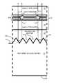
- FIG. 1provides a cross-section view of one embodiment of a reflecting light emitting structure 10 according to the present disclosure.
- the reflecting light emitting structure 10includes a substrate 12 having a first face 14 and a second face 16 .
- the substrate 12is preferably made of a material that has a uniform crystalline structure.
- a silicon (Si) wafer like those commonly used in integrated circuit manufacturingis suitable as the substrate 12 .
- a plurality of grooves 18is fabricated into the first face 14 of the substrate 12 .
- the plurality of grooves 18is preferably anisotropically etched into the first face 14 of the substrate 12 using wet chemistry.
- a wet chemistry etchantsuch as potassium hydroxide (KOH) is usable to etch the plurality of grooves 18 .
- the plurality of grooves 18Due to the crystalline structure of the substrate 12 , the plurality of grooves 18 has uniformity across the first face 14 of the substrate 12 .
- each of the plurality of grooves 18includes a first sidewall 20 that is coplanar with a second crystallographic plane and a second sidewall 22 that is coplanar with a third crystallographic plane.
- the first sidewall 20is inclined at a first slope with respect to the first face 14 of the substrate 12
- the second sidewall 22is inclined at a second slope with respect to the first face 14 of the substrate 12 .
- the first sidewall 20intersects the second sidewall 22 to define a V-shape for each of the plurality of grooves 18 formed in the first face 14 of the substrate 12 .
- a channel width (W) and a depth (D) of each of the plurality of grooves 18is controllable by the etchant concentration, the etchant temperature, and the etching duration.
- the dimension Wis typically larger than a desired wavelength of a light emission produced by the reflecting light emitting structure 10 .
- the dimension Wwill have a range of 0.1 micrometers ( ⁇ m) to 2 ⁇ m, and preferably around 0.5 ⁇ m. Both the dimensions W and D typically correspond to a single-digit number of wavelengths of the light emission.
- FIGS. 2A , 2 B and 2 Cdepict three typical crystallographic planes that are defined by Miller indices and unit cells for Si.
- FIG. 2Ashows the ⁇ 100> crystallographic plane that is usable as the first face 14 ( FIG. 1 ) of the reflecting light emitting structure 10 .
- Hydroxide chemistrymay be used to etch the ⁇ 100> crystallographic plane to expose a plurality of ⁇ 111> planes.
- An orientation for a ⁇ 111> planeis illustrated in FIG. 2B .
- a ⁇ 111> planeslopes at an angle of approximately 54° with respect to a ⁇ 100> plane.
- the present disclosureis not limited to ⁇ 100> and ⁇ 111> crystallographic planes.
- Other crystallographic planessuch as the ⁇ 110> crystallographic planes may be used to form the plurality of grooves 18 ( FIG. 1 ).
- a ⁇ 110> planeslopes at an angle of 45° with respect to the ⁇ 100> plane.
- Which particular crystallographic planes are exposed by wet chemistry etchingis a function of concentration of etchants, etchant temperature, and etching duration among other factors that are well-known in the prior art. Even mechanical grinding can be used to exposed crystallographic planes to fabricate the plurality of grooves 18 .
- a buffer layer 24is provided on the substrate 12 .
- the buffer layer 24may be grown or deposited on the substrate 12 .
- the buffer layer 24may comprise sub-layers of aluminum nitride (AlN) and various compounds of aluminum gallium nitride (Al x Ga 1-x N), wherein x is greater than zero but less than or equal to one.
- the substrate 12may comprise AlN.
- the substrate 12may be made of a plurality of layers of Al x Ga 1-x N (0 ⁇ x ⁇ 1).
- a first doped layer 26is provided on the buffer layer 24 .
- the first doped layer 26may be deposited or grown on the buffer layer 24 .
- the first doped layer 26is made of n-type GaN.
- a multiple quantum well (MQW) structure layer 28is grown on the first doped layer 26 , and a second doped layer 30 is deposited onto the MQW structure layer 28 .
- the first doped layer 26 , the MQW structure layer 28 , and the second doped layer 30make up a light emitting diode (LED) 32 .
- LEDlight emitting diode
- a first electrical contact 34is provided on the second doped layer 30 .
- the first electrical contact 34 and an associated bonding conductor 36are usable to electrically couple the second doped layer 30 to an external circuit terminal (not shown).
- a second electrical contact 38is provided on the first doped layer 26 .
- the second electrical contact 38 and an associated bonding conductor 40are usable to electrically couple the first doped layer 26 to another external circuit terminal (not shown).
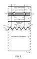
- FIG. 3depicts a section of the reflecting light emitting structure 10 ( FIG. 1 ) that illustrates the operation of the reflecting light emitting structure 10 according to the present disclosure.
- Light rays L 1 , L 2 , L 3 , and L 4are symbolic of the total light emission generated by the LED 32 .
- the buffer layer 24 , the first doped layer 26 , and the second doped layer 30are significantly non-opaque to the light rays L 2 and L 4 .
- the substrate 12being made of Si, is opaque to the light emission. Therefore light emission, such as that represented by light rays L 2 and L 4 , that is initially directed towards the substrate 12 needs to be reflected back through the LED 32 in order not to be absorbed and wasted.
- the plurality of grooves 18is ideal for reflecting and redirecting the light emission back through the LED 32 to open space.
- a light emissionproduces the light ray L 1 , which propagates directly out of the LED 32 towards open space, but the light ray L 2 initially propagates towards the substrate 12 .
- the light ray L 2is reflected by the second sidewall 22 of one of the plurality of grooves 18 .
- the first sidewall 20 of the same one of the plurality of grooves 18reflects the light ray L 2 through the LED 32 towards open space.
- the light ray L 4is reflected and redirected towards open space in the direction of the light ray L 3 .
- FIG. 4is a flowchart depicting a method of fabricating the reflecting light emitting structure 10 ( FIG. 1 ). The method begins by providing the substrate 12 with the first face 14 in a first crystallographic plane in a first orientation (step 100 ).
- the substrate 12is made of Si.
- etching the plurality of grooves 18 in the first face 14 of the substrate 12may begin (step 102 ).
- an anisotropic wet etchantsuch as KOH is used to fabricate the first sidewall 20 and the second sidewall 22 of the plurality of grooves 18 , such that each of the plurality of grooves 18 becomes uniform and regularly spaced with respect to each other as etching proceeds.
- the duration of the etching and temperature of the etchantis monitored (step 104 ).
- a determinationis made as to when the W of each of the plurality of grooves 18 has reached a desired value based upon the etchant temperature, the concentration of etchant, and the duration of the etching process (step 106 ). If the desired value of width W of each of the plurality of grooves 18 has not been reached, the etching process continues with step 104 . Otherwise, etching of the substrate 12 is stopped to clean and dry the substrate 12 (step 108 ).
- Another stepincludes providing the buffer layer 24 on the first face 14 of the substrate 12 (step 110 ).
- the buffer layer 24may be grown or deposited on the substrate 12 .
- the buffer layer 24may comprise sub-layers of AlN and various compounds of Al x Ga 1-x N, wherein x is greater than zero but less than or equal to one. Alternately, the buffer layer 24 may comprise only AlN. Further still, the buffer layer 24 may be made of a plurality of layers made of Al x Ga 1-x N (0 ⁇ x ⁇ 1).
- the fabrication of the LED 32begins by providing the first doped layer 26 on the buffer layer 24 (step 112 ).
- the step 112is accomplished by depositing or growing the first doped layer 26 on the buffer layer 24 .
- the first doped layer 26is also preferable for the first doped layer 26 to be made of n-type doped GaN.
- a step of fabricating the MQW structure layer 28 onto the first doped layer 26is performed using standard MQW fabrication technology (step 114 ).
- Another stepcompletes the LED 32 by providing the second doped layer 30 on the MQW structure layer 28 (step 116 ).
- the step 116 providing the second doped layer 30is preferably accomplished by depositing or growing p-type doped GaN onto the MQW structure layer 28 .
- the first electrical contact 34is preferably made of a material that is the same type as the second doped layer 30 .
- the second doped layer 30is made of n-type material, then the first electrical contact 34 should also be made of n-type material.
- a next stepincludes etching through the second doped layer 30 and the MQW structure layer 28 to expose a section of the first doped layer 26 (step 120 ).
- Another stepinvolves providing the second electrical contact 38 on the first doped layer 26 (step 122 ).
Landscapes
- Led Devices (AREA)
Abstract
Description
- This application claims the benefit of provisional patent application Ser. No. 61/227,630, filed Jul. 22, 2009, the disclosure of which is hereby incorporated herein by reference in its entirety. The application also relates to provisional patent application Ser. No. 61/227,624, filed Jul. 22, 2009, and to utility patent application Ser. No. 12/705,869 filed Feb. 15, 2010, both of which are hereby incorporated herein by reference in their entireties.
- The present disclosure relates to a structure and fabrication method for a reflecting light emitting structure that includes a textured substrate, and in particular to a textured substrate having uniform grooves.
- Prior art solid state lighting systems use gallium nitride (GaN) that is grown on 150 millimeter (mm) silicon (Si) wafers. Light extraction efficiency is often improved for light emitting diodes (LEDs) grown on sapphire or silicon carbide (SiC) by texturing a surface of the LED structure. The texturing improves light extraction efficiency by reducing internal reflections that occur at internal surfaces of the LED structure.
- Si substrates are attractive over sapphire and SiC substrates due to being relatively less expensive than sapphire and SiC substrates. Moreover, Si substrates are attractive for GaN-based devices in that Si device manufacturing is based upon a mature Si device fabrication technology. However, relatively complex and expensive packaging is required to efficiently scatter light emissions from a GaN LED structure. Thus, there is a need for a reflecting light emitting structure that incorporates a Si substrate.
- The present disclosure provides a reflecting light emitting structure and method of manufacture that incorporates a silicon (Si) substrate having a uniformly textured surface. Light emissions from a light emitting diode (LED) are efficiently scattered by the uniformly textured surface of the Si substrate. The light reflecting structure of the present disclosure is particularly well suited for efficiently reflecting light generated by a gallium nitride (GaN) LED that emits blue light.
- The disclosed reflecting light emitting structure includes a substrate having a first face and a second face, wherein the first face is in a first crystallographic plane. A plurality of grooves is formed in the first face of the substrate, wherein each of the plurality of grooves includes a first sidewall that is coplanar with a second crystallographic plane and a second sidewall that is coplanar with a third crystallographic plane. A buffer layer is provided on the substrate to reduce mechanical strain between the substrate and an LED fabricated on the buffer layer.
- Those skilled in the art will appreciate the scope of the present disclosure and realize additional aspects thereof after reading the following detailed description of the preferred embodiments in association with the accompanying drawing figures.
- The accompanying drawing figures incorporated in and forming a part of this specification illustrate several aspects of the disclosure, and together with the description serve to explain the principles of the disclosure.
FIG. 1 is a cross-section view of one embodiment of a reflecting light emitting structure according to the present disclosure.FIG. 2A is a unit cell for silicon (Si) that shows a <100> crystallographic plane.FIG. 2B is a unit cell for Si that shows a <111> crystallographic plane.FIG. 2C is a unit cell for Si that shows a <110> crystallographic plane.FIG. 3 depicts a section of the reflecting light emitting structure that illustrates the operation of the reflecting light structure according to the present disclosure.FIG. 4 is a flowchart of a method of manufacture for a reflecting light emitting structure according to the present disclosure.- The embodiments set forth below represent the necessary information to enable those skilled in the art to practice the disclosure and illustrate the best mode of practicing the disclosure. Upon reading the following description in light of the accompanying drawing figures, those skilled in the art will understand the concepts of the disclosure and will recognize applications of these concepts not particularly addressed herein. It should be understood that these concepts and applications fall within the scope of the disclosure and the accompanying claims.
FIG. 1 provides a cross-section view of one embodiment of a reflectinglight emitting structure 10 according to the present disclosure. The reflectinglight emitting structure 10 includes asubstrate 12 having afirst face 14 and asecond face 16. Thesubstrate 12 is preferably made of a material that has a uniform crystalline structure. A silicon (Si) wafer like those commonly used in integrated circuit manufacturing is suitable as thesubstrate 12. A plurality ofgrooves 18 is fabricated into thefirst face 14 of thesubstrate 12. The plurality ofgrooves 18 is preferably anisotropically etched into thefirst face 14 of thesubstrate 12 using wet chemistry.- A wet chemistry etchant such as potassium hydroxide (KOH) is usable to etch the plurality of
grooves 18. Due to the crystalline structure of thesubstrate 12, the plurality ofgrooves 18 has uniformity across thefirst face 14 of thesubstrate 12. As shown inFIG. 1 , each of the plurality ofgrooves 18 includes afirst sidewall 20 that is coplanar with a second crystallographic plane and asecond sidewall 22 that is coplanar with a third crystallographic plane. Thefirst sidewall 20 is inclined at a first slope with respect to thefirst face 14 of thesubstrate 12, and thesecond sidewall 22 is inclined at a second slope with respect to thefirst face 14 of thesubstrate 12. Thefirst sidewall 20 intersects thesecond sidewall 22 to define a V-shape for each of the plurality ofgrooves 18 formed in thefirst face 14 of thesubstrate 12. - A channel width (W) and a depth (D) of each of the plurality of
grooves 18 is controllable by the etchant concentration, the etchant temperature, and the etching duration. The dimension W is typically larger than a desired wavelength of a light emission produced by the reflectinglight emitting structure 10. For a gallium nitride (GaN) light emission, the dimension W will have a range of 0.1 micrometers (μm) to 2 μm, and preferably around 0.5 μm. Both the dimensions W and D typically correspond to a single-digit number of wavelengths of the light emission. FIGS. 2A ,2B and2C depict three typical crystallographic planes that are defined by Miller indices and unit cells for Si. In particular,FIG. 2A shows the <100> crystallographic plane that is usable as the first face14 (FIG. 1 ) of the reflectinglight emitting structure 10. Hydroxide chemistry may be used to etch the <100> crystallographic plane to expose a plurality of <111> planes. An orientation for a <111> plane is illustrated inFIG. 2B . A <111> plane slopes at an angle of approximately 54° with respect to a <100> plane.- The present disclosure is not limited to <100> and <111> crystallographic planes. Other crystallographic planes such as the <110> crystallographic planes may be used to form the plurality of grooves18 (
FIG. 1 ). A <110> plane slopes at an angle of 45° with respect to the <100> plane. Which particular crystallographic planes are exposed by wet chemistry etching is a function of concentration of etchants, etchant temperature, and etching duration among other factors that are well-known in the prior art. Even mechanical grinding can be used to exposed crystallographic planes to fabricate the plurality ofgrooves 18. - Turning back to
FIG. 1 , abuffer layer 24 is provided on thesubstrate 12. Thebuffer layer 24 may be grown or deposited on thesubstrate 12. Thebuffer layer 24 may comprise sub-layers of aluminum nitride (AlN) and various compounds of aluminum gallium nitride (AlxGa1-xN), wherein x is greater than zero but less than or equal to one. Alternately, thesubstrate 12 may comprise AlN. Further still, thesubstrate 12 may be made of a plurality of layers of AlxGa1-xN (0<x≦1). - A first doped
layer 26 is provided on thebuffer layer 24. The first dopedlayer 26 may be deposited or grown on thebuffer layer 24. Preferably the first dopedlayer 26 is made of n-type GaN. A multiple quantum well (MQW)structure layer 28 is grown on the first dopedlayer 26, and a second dopedlayer 30 is deposited onto theMQW structure layer 28. The first dopedlayer 26, theMQW structure layer 28, and the second dopedlayer 30 make up a light emitting diode (LED)32. - A first
electrical contact 34 is provided on the second dopedlayer 30. The firstelectrical contact 34 and an associatedbonding conductor 36 are usable to electrically couple the second dopedlayer 30 to an external circuit terminal (not shown). A secondelectrical contact 38 is provided on the first dopedlayer 26. The secondelectrical contact 38 and an associatedbonding conductor 40 are usable to electrically couple the first dopedlayer 26 to another external circuit terminal (not shown). FIG. 3 depicts a section of the reflecting light emitting structure10 (FIG. 1 ) that illustrates the operation of the reflectinglight emitting structure 10 according to the present disclosure. Light rays L1, L2, L3, and L4 are symbolic of the total light emission generated by theLED 32. Thebuffer layer 24, the first dopedlayer 26, and the second dopedlayer 30 are significantly non-opaque to the light rays L2 and L4. However, thesubstrate 12, being made of Si, is opaque to the light emission. Therefore light emission, such as that represented by light rays L2 and L4, that is initially directed towards thesubstrate 12 needs to be reflected back through theLED 32 in order not to be absorbed and wasted. The plurality ofgrooves 18 is ideal for reflecting and redirecting the light emission back through theLED 32 to open space. For example, a light emission produces the light ray L1, which propagates directly out of theLED 32 towards open space, but the light ray L2 initially propagates towards thesubstrate 12. However, the light ray L2 is reflected by thesecond sidewall 22 of one of the plurality ofgrooves 18. Thefirst sidewall 20 of the same one of the plurality ofgrooves 18 reflects the light ray L2 through theLED 32 towards open space. In similar fashion, the light ray L4 is reflected and redirected towards open space in the direction of the light ray L3.FIG. 4 is a flowchart depicting a method of fabricating the reflecting light emitting structure10 (FIG. 1 ). The method begins by providing thesubstrate 12 with thefirst face 14 in a first crystallographic plane in a first orientation (step100). In a preferred embodiment, thesubstrate 12 is made of Si.- At this point, etching the plurality of
grooves 18 in thefirst face 14 of thesubstrate 12 may begin (step102). Preferably, an anisotropic wet etchant such as KOH is used to fabricate thefirst sidewall 20 and thesecond sidewall 22 of the plurality ofgrooves 18, such that each of the plurality ofgrooves 18 becomes uniform and regularly spaced with respect to each other as etching proceeds. - While the etching of the plurality of
grooves 18 proceeds, the duration of the etching and temperature of the etchant is monitored (step104). A determination is made as to when the W of each of the plurality ofgrooves 18 has reached a desired value based upon the etchant temperature, the concentration of etchant, and the duration of the etching process (step106). If the desired value of width W of each of the plurality ofgrooves 18 has not been reached, the etching process continues withstep 104. Otherwise, etching of thesubstrate 12 is stopped to clean and dry the substrate12 (step108). - Another step includes providing the
buffer layer 24 on thefirst face 14 of the substrate12 (step110). Thebuffer layer 24 may be grown or deposited on thesubstrate 12. Thebuffer layer 24 may comprise sub-layers of AlN and various compounds of AlxGa1-xN, wherein x is greater than zero but less than or equal to one. Alternately, thebuffer layer 24 may comprise only AlN. Further still, thebuffer layer 24 may be made of a plurality of layers made of AlxGa1-xN (0<x≦1). - Other steps include fabricating the LED32 (
FIG. 1 ). The fabrication of theLED 32 begins by providing the first dopedlayer 26 on the buffer layer24 (step112). Preferably, thestep 112 is accomplished by depositing or growing the first dopedlayer 26 on thebuffer layer 24. It is also preferable for the first dopedlayer 26 to be made of n-type doped GaN. - In order to allow the reflecting
light emitting structure 10 to emit light efficiently, a step of fabricating theMQW structure layer 28 onto the first dopedlayer 26 is performed using standard MQW fabrication technology (step114). - Another step completes the
LED 32 by providing the second dopedlayer 30 on the MQW structure layer28 (step116). Thestep 116 providing the second dopedlayer 30 is preferably accomplished by depositing or growing p-type doped GaN onto theMQW structure layer 28. - Next, a series of steps is performed to make electrical connections between external electrical circuitry (not shown) and the
LED 32. These steps may begin by providing the firstelectrical contact 34 on the second doped layer30 (step118). The firstelectrical contact 34 is preferably made of a material that is the same type as the second dopedlayer 30. For example, if the second dopedlayer 30 is made of n-type material, then the firstelectrical contact 34 should also be made of n-type material. - A next step includes etching through the second doped
layer 30 and theMQW structure layer 28 to expose a section of the first doped layer26 (step120). Another step involves providing the secondelectrical contact 38 on the first doped layer26 (step122). - Those skilled in the art will recognize improvements and modifications to the preferred embodiments of the present disclosure. All such improvements and modifications are considered within the scope of the concepts disclosed herein and the claims that follow.
Claims (20)
Priority Applications (1)
| Application Number | Priority Date | Filing Date | Title |
|---|---|---|---|
| US12/841,225US8405068B2 (en) | 2009-07-22 | 2010-07-22 | Reflecting light emitting structure and method of manufacture thereof |
Applications Claiming Priority (2)
| Application Number | Priority Date | Filing Date | Title |
|---|---|---|---|
| US22763009P | 2009-07-22 | 2009-07-22 | |
| US12/841,225US8405068B2 (en) | 2009-07-22 | 2010-07-22 | Reflecting light emitting structure and method of manufacture thereof |
Publications (2)
| Publication Number | Publication Date |
|---|---|
| US20110101300A1true US20110101300A1 (en) | 2011-05-05 |
| US8405068B2 US8405068B2 (en) | 2013-03-26 |
Family
ID=43496489
Family Applications (2)
| Application Number | Title | Priority Date | Filing Date |
|---|---|---|---|
| US12/841,257AbandonedUS20110017972A1 (en) | 2009-07-22 | 2010-07-22 | Light emitting structure with integral reverse voltage protection |
| US12/841,225Expired - Fee RelatedUS8405068B2 (en) | 2009-07-22 | 2010-07-22 | Reflecting light emitting structure and method of manufacture thereof |
Family Applications Before (1)
| Application Number | Title | Priority Date | Filing Date |
|---|---|---|---|
| US12/841,257AbandonedUS20110017972A1 (en) | 2009-07-22 | 2010-07-22 | Light emitting structure with integral reverse voltage protection |
Country Status (1)
| Country | Link |
|---|---|
| US (2) | US20110017972A1 (en) |
Cited By (14)
| Publication number | Priority date | Publication date | Assignee | Title |
|---|---|---|---|---|
| US8988097B2 (en) | 2012-08-24 | 2015-03-24 | Rf Micro Devices, Inc. | Method for on-wafer high voltage testing of semiconductor devices |
| US9070761B2 (en) | 2012-08-27 | 2015-06-30 | Rf Micro Devices, Inc. | Field effect transistor (FET) having fingers with rippled edges |
| US9093420B2 (en) | 2012-04-18 | 2015-07-28 | Rf Micro Devices, Inc. | Methods for fabricating high voltage field effect transistor finger terminations |
| US9124221B2 (en) | 2012-07-16 | 2015-09-01 | Rf Micro Devices, Inc. | Wide bandwidth radio frequency amplier having dual gate transistors |
| US9129802B2 (en) | 2012-08-27 | 2015-09-08 | Rf Micro Devices, Inc. | Lateral semiconductor device with vertical breakdown region |
| US9142620B2 (en) | 2012-08-24 | 2015-09-22 | Rf Micro Devices, Inc. | Power device packaging having backmetals couple the plurality of bond pads to the die backside |
| US9147632B2 (en) | 2012-08-24 | 2015-09-29 | Rf Micro Devices, Inc. | Semiconductor device having improved heat dissipation |
| US9202874B2 (en) | 2012-08-24 | 2015-12-01 | Rf Micro Devices, Inc. | Gallium nitride (GaN) device with leakage current-based over-voltage protection |
| US9325281B2 (en) | 2012-10-30 | 2016-04-26 | Rf Micro Devices, Inc. | Power amplifier controller |
| US9455327B2 (en) | 2014-06-06 | 2016-09-27 | Qorvo Us, Inc. | Schottky gated transistor with interfacial layer |
| US9536803B2 (en) | 2014-09-05 | 2017-01-03 | Qorvo Us, Inc. | Integrated power module with improved isolation and thermal conductivity |
| US9917080B2 (en) | 2012-08-24 | 2018-03-13 | Qorvo US. Inc. | Semiconductor device with electrical overstress (EOS) protection |
| US10062684B2 (en) | 2015-02-04 | 2018-08-28 | Qorvo Us, Inc. | Transition frequency multiplier semiconductor device |
| US10615158B2 (en) | 2015-02-04 | 2020-04-07 | Qorvo Us, Inc. | Transition frequency multiplier semiconductor device |
Families Citing this family (13)
| Publication number | Priority date | Publication date | Assignee | Title |
|---|---|---|---|---|
| KR100659373B1 (en)* | 2006-02-09 | 2006-12-19 | 서울옵토디바이스주식회사 | Patterned light emitting diode substrate and light emitting diode adopting the same |
| TWI446578B (en)* | 2010-09-23 | 2014-07-21 | Epistar Corp | Light-emitting element and its manufacturing method |
| TW201401552A (en)* | 2012-06-19 | 2014-01-01 | High Power Optoelectronics Inc | Thermal stress release structure for light emitting diodes |
| US8552457B1 (en)* | 2012-08-07 | 2013-10-08 | High Power Opto. Inc. | Thermal stress releasing structure of a light-emitting diode |
| CN103187499B (en)* | 2013-03-07 | 2015-11-25 | 天津三安光电有限公司 | Light-emitting Diode And Its Making Method |
| EP3100589A1 (en) | 2014-01-31 | 2016-12-07 | Arçelik Anonim Sirketi | Circuit arrangement minimizing reverse voltage drop across a light emitting diode |
| US11289593B2 (en)* | 2015-07-31 | 2022-03-29 | Infineon Technologies Austria Ag | Breakdown resistant HEMT substrate and device |
| JP2017059700A (en)* | 2015-09-17 | 2017-03-23 | サンケン電気株式会社 | Semiconductor light emitting device and manufacturing method of the same |
| CN106025017B (en)* | 2016-06-01 | 2019-01-15 | 天津三安光电有限公司 | Light emitting diode and preparation method thereof with electrostatic protection |
| WO2018038927A1 (en) | 2016-08-26 | 2018-03-01 | The Penn State Research Foundation | High light-extraction efficiency (lee) light-emitting diode (led) |
| CN108400133B (en)* | 2018-05-11 | 2025-03-25 | 广东工业大学 | A method for preparing a deep ultraviolet LED epitaxial structure with a same-side structure |
| WO2019219366A1 (en) | 2018-05-18 | 2019-11-21 | Arcelik Anonim Sirketi | Circuit configuration canceling out reverse voltage drop in a light emitting diode (led) |
| CN109065687A (en)* | 2018-07-17 | 2018-12-21 | 佛山市国星半导体技术有限公司 | A kind of pressure stabilizing LED epitaxial structure and preparation method thereof, LED chip and LED lamp tube |
Citations (24)
| Publication number | Priority date | Publication date | Assignee | Title |
|---|---|---|---|---|
| US5389571A (en)* | 1991-12-18 | 1995-02-14 | Hiroshi Amano | Method of fabricating a gallium nitride based semiconductor device with an aluminum and nitrogen containing intermediate layer |
| US5764673A (en)* | 1995-09-25 | 1998-06-09 | Mitsubishi Denki Kabushiki Kaisha | Semiconductor light emitting device |
| US5914501A (en)* | 1998-08-27 | 1999-06-22 | Hewlett-Packard Company | Light emitting diode assembly having integrated electrostatic discharge protection |
| US6133589A (en)* | 1999-06-08 | 2000-10-17 | Lumileds Lighting, U.S., Llc | AlGaInN-based LED having thick epitaxial layer for improved light extraction |
| US6376864B1 (en)* | 1999-07-06 | 2002-04-23 | Tien Yang Wang | Semiconductor light-emitting device and method for manufacturing the same |
| US20030122139A1 (en)* | 2001-12-28 | 2003-07-03 | United Epitaxy Co., Ltd. | Light emitting diode package structure having an electro-static protective diode |
| US6593597B2 (en)* | 2001-06-05 | 2003-07-15 | South Epitaxy Corporation | Group III-V element-based LED having ESD protection capacity |
| US6861677B2 (en)* | 2002-03-04 | 2005-03-01 | United Epitaxy Co., Ltd. | Package of lightemitting diode with protective element |
| US20050271107A1 (en)* | 2004-06-08 | 2005-12-08 | Fuji Xerox Co., Ltd. | Semiconductor laser apparatus and manufacturing method thereof |
| US20060043385A1 (en)* | 2004-08-27 | 2006-03-02 | Institute Of Semiconductors, Chinese Academy Of Sciences | White light emitting diode of a blue and yellow light emitting (structure) layer stacked structure and method of manufacturing the same |
| US7015512B2 (en)* | 2003-12-20 | 2006-03-21 | Samsung Electro-Mechanics Co., Ltd. | High power flip chip LED |
| US20060068601A1 (en)* | 2004-09-29 | 2006-03-30 | Jeong-Sik Lee | Wafer for compound semiconductor devices, and method of fabrication |
| US7042150B2 (en)* | 2002-12-20 | 2006-05-09 | Showa Denko K.K. | Light-emitting device, method of fabricating the device, and LED lamp using the device |
| US7053420B2 (en)* | 2001-03-21 | 2006-05-30 | Mitsubishi Cable Industries, Ltd. | GaN group semiconductor light-emitting element with concave and convex structures on the substrate and a production method thereof |
| US20060243988A1 (en)* | 2005-05-02 | 2006-11-02 | Nichia Corporation | Nitride semiconductor element |
| US20070093009A1 (en)* | 2000-05-26 | 2007-04-26 | Commissariat A L'energie Atomique | Semiconductor device with vertical electron injection and its manufacturing method |
| US7211822B2 (en)* | 1997-01-09 | 2007-05-01 | Nichia Chemical Industries, Ltd. | Nitride semiconductor device |
| US20070295985A1 (en)* | 2001-02-23 | 2007-12-27 | Nitronex Corporation | Gallium nitride material devices and methods of forming the same |
| US20080112448A1 (en)* | 2006-11-09 | 2008-05-15 | Tetsuzo Ueda | Nitride semiconductor laser diode |
| US20080121876A1 (en)* | 2005-07-13 | 2008-05-29 | Sanken Electric Co., Ltd. | Surface-stabilized semiconductor device |
| US20080272382A1 (en)* | 2006-03-07 | 2008-11-06 | Lg Electronics Inc. | Light emitting device and method of manufacturing the same |
| US20080283821A1 (en)* | 2007-05-17 | 2008-11-20 | Samsung Corning Co., Ltd. | Method of growing gan crystal on silicon substrate, and light emitting device and method of manufacturing thereof |
| US20100133567A1 (en)* | 2007-05-21 | 2010-06-03 | Lg Innotek Co., Ltd | Semiconductor light emitting device and method of manufacturing the same |
| US20110163342A1 (en)* | 2007-07-23 | 2011-07-07 | Kyung Jun Kim | Light emitting device |
Family Cites Families (5)
| Publication number | Priority date | Publication date | Assignee | Title |
|---|---|---|---|---|
| JPH10242584A (en) | 1997-02-28 | 1998-09-11 | Hitachi Ltd | Semiconductor light emitting device |
| JP3534227B2 (en) | 1998-07-10 | 2004-06-07 | 株式会社村田製作所 | Semiconductor light emitting device |
| WO2001061766A1 (en) | 2000-02-21 | 2001-08-23 | Sanken Electric Co., Ltd. | Light-emitting semiconductor device and method of manufacture thereof |
| JP3889662B2 (en) | 2002-05-10 | 2007-03-07 | 三菱電線工業株式会社 | GaN-based semiconductor light emitting device manufacturing method |
| US7115896B2 (en) | 2002-12-04 | 2006-10-03 | Emcore Corporation | Semiconductor structures for gallium nitride-based devices |
- 2010
- 2010-07-22USUS12/841,257patent/US20110017972A1/ennot_activeAbandoned
- 2010-07-22USUS12/841,225patent/US8405068B2/ennot_activeExpired - Fee Related
Patent Citations (25)
| Publication number | Priority date | Publication date | Assignee | Title |
|---|---|---|---|---|
| US5389571A (en)* | 1991-12-18 | 1995-02-14 | Hiroshi Amano | Method of fabricating a gallium nitride based semiconductor device with an aluminum and nitrogen containing intermediate layer |
| US5764673A (en)* | 1995-09-25 | 1998-06-09 | Mitsubishi Denki Kabushiki Kaisha | Semiconductor light emitting device |
| US20100025657A1 (en)* | 1997-01-09 | 2010-02-04 | Shinichi Nagahama | Nitride semiconductor device |
| US7211822B2 (en)* | 1997-01-09 | 2007-05-01 | Nichia Chemical Industries, Ltd. | Nitride semiconductor device |
| US5914501A (en)* | 1998-08-27 | 1999-06-22 | Hewlett-Packard Company | Light emitting diode assembly having integrated electrostatic discharge protection |
| US6133589A (en)* | 1999-06-08 | 2000-10-17 | Lumileds Lighting, U.S., Llc | AlGaInN-based LED having thick epitaxial layer for improved light extraction |
| US6376864B1 (en)* | 1999-07-06 | 2002-04-23 | Tien Yang Wang | Semiconductor light-emitting device and method for manufacturing the same |
| US20070093009A1 (en)* | 2000-05-26 | 2007-04-26 | Commissariat A L'energie Atomique | Semiconductor device with vertical electron injection and its manufacturing method |
| US20070295985A1 (en)* | 2001-02-23 | 2007-12-27 | Nitronex Corporation | Gallium nitride material devices and methods of forming the same |
| US7053420B2 (en)* | 2001-03-21 | 2006-05-30 | Mitsubishi Cable Industries, Ltd. | GaN group semiconductor light-emitting element with concave and convex structures on the substrate and a production method thereof |
| US6593597B2 (en)* | 2001-06-05 | 2003-07-15 | South Epitaxy Corporation | Group III-V element-based LED having ESD protection capacity |
| US20030122139A1 (en)* | 2001-12-28 | 2003-07-03 | United Epitaxy Co., Ltd. | Light emitting diode package structure having an electro-static protective diode |
| US6861677B2 (en)* | 2002-03-04 | 2005-03-01 | United Epitaxy Co., Ltd. | Package of lightemitting diode with protective element |
| US7042150B2 (en)* | 2002-12-20 | 2006-05-09 | Showa Denko K.K. | Light-emitting device, method of fabricating the device, and LED lamp using the device |
| US7015512B2 (en)* | 2003-12-20 | 2006-03-21 | Samsung Electro-Mechanics Co., Ltd. | High power flip chip LED |
| US20050271107A1 (en)* | 2004-06-08 | 2005-12-08 | Fuji Xerox Co., Ltd. | Semiconductor laser apparatus and manufacturing method thereof |
| US20060043385A1 (en)* | 2004-08-27 | 2006-03-02 | Institute Of Semiconductors, Chinese Academy Of Sciences | White light emitting diode of a blue and yellow light emitting (structure) layer stacked structure and method of manufacturing the same |
| US20060068601A1 (en)* | 2004-09-29 | 2006-03-30 | Jeong-Sik Lee | Wafer for compound semiconductor devices, and method of fabrication |
| US20060243988A1 (en)* | 2005-05-02 | 2006-11-02 | Nichia Corporation | Nitride semiconductor element |
| US20080121876A1 (en)* | 2005-07-13 | 2008-05-29 | Sanken Electric Co., Ltd. | Surface-stabilized semiconductor device |
| US20080272382A1 (en)* | 2006-03-07 | 2008-11-06 | Lg Electronics Inc. | Light emitting device and method of manufacturing the same |
| US20080112448A1 (en)* | 2006-11-09 | 2008-05-15 | Tetsuzo Ueda | Nitride semiconductor laser diode |
| US20080283821A1 (en)* | 2007-05-17 | 2008-11-20 | Samsung Corning Co., Ltd. | Method of growing gan crystal on silicon substrate, and light emitting device and method of manufacturing thereof |
| US20100133567A1 (en)* | 2007-05-21 | 2010-06-03 | Lg Innotek Co., Ltd | Semiconductor light emitting device and method of manufacturing the same |
| US20110163342A1 (en)* | 2007-07-23 | 2011-07-07 | Kyung Jun Kim | Light emitting device |
Cited By (17)
| Publication number | Priority date | Publication date | Assignee | Title |
|---|---|---|---|---|
| US9136341B2 (en) | 2012-04-18 | 2015-09-15 | Rf Micro Devices, Inc. | High voltage field effect transistor finger terminations |
| US9564497B2 (en) | 2012-04-18 | 2017-02-07 | Qorvo Us, Inc. | High voltage field effect transitor finger terminations |
| US9093420B2 (en) | 2012-04-18 | 2015-07-28 | Rf Micro Devices, Inc. | Methods for fabricating high voltage field effect transistor finger terminations |
| US9124221B2 (en) | 2012-07-16 | 2015-09-01 | Rf Micro Devices, Inc. | Wide bandwidth radio frequency amplier having dual gate transistors |
| US9202874B2 (en) | 2012-08-24 | 2015-12-01 | Rf Micro Devices, Inc. | Gallium nitride (GaN) device with leakage current-based over-voltage protection |
| US9142620B2 (en) | 2012-08-24 | 2015-09-22 | Rf Micro Devices, Inc. | Power device packaging having backmetals couple the plurality of bond pads to the die backside |
| US9147632B2 (en) | 2012-08-24 | 2015-09-29 | Rf Micro Devices, Inc. | Semiconductor device having improved heat dissipation |
| US8988097B2 (en) | 2012-08-24 | 2015-03-24 | Rf Micro Devices, Inc. | Method for on-wafer high voltage testing of semiconductor devices |
| US9640632B2 (en) | 2012-08-24 | 2017-05-02 | Qorvo Us, Inc. | Semiconductor device having improved heat dissipation |
| US9917080B2 (en) | 2012-08-24 | 2018-03-13 | Qorvo US. Inc. | Semiconductor device with electrical overstress (EOS) protection |
| US9129802B2 (en) | 2012-08-27 | 2015-09-08 | Rf Micro Devices, Inc. | Lateral semiconductor device with vertical breakdown region |
| US9070761B2 (en) | 2012-08-27 | 2015-06-30 | Rf Micro Devices, Inc. | Field effect transistor (FET) having fingers with rippled edges |
| US9325281B2 (en) | 2012-10-30 | 2016-04-26 | Rf Micro Devices, Inc. | Power amplifier controller |
| US9455327B2 (en) | 2014-06-06 | 2016-09-27 | Qorvo Us, Inc. | Schottky gated transistor with interfacial layer |
| US9536803B2 (en) | 2014-09-05 | 2017-01-03 | Qorvo Us, Inc. | Integrated power module with improved isolation and thermal conductivity |
| US10062684B2 (en) | 2015-02-04 | 2018-08-28 | Qorvo Us, Inc. | Transition frequency multiplier semiconductor device |
| US10615158B2 (en) | 2015-02-04 | 2020-04-07 | Qorvo Us, Inc. | Transition frequency multiplier semiconductor device |
Also Published As
| Publication number | Publication date |
|---|---|
| US8405068B2 (en) | 2013-03-26 |
| US20110017972A1 (en) | 2011-01-27 |
Similar Documents
| Publication | Publication Date | Title |
|---|---|---|
| US8405068B2 (en) | Reflecting light emitting structure and method of manufacture thereof | |
| KR101629984B1 (en) | Method for producing an optoelectronic component and optoelectronic component | |
| TWI487133B (en) | Roughened high refractive index index layer / LED for high light extraction | |
| US7687376B2 (en) | Method of manufacturing vertical gallium nitride-based light emitting diode | |
| US8395167B2 (en) | External light efficiency of light emitting diodes | |
| TWI472061B (en) | Externally extracted light-emitting diodes modified according to the surface of the crystal facet | |
| EP2160772B1 (en) | Semiconductor light emitting device | |
| US8034647B2 (en) | LED with substrate modifications for enhanced light extraction and method of making same | |
| US8476643B2 (en) | Radiation-emitting body and method for producing a radiation-emitting body | |
| EP3149781B1 (en) | Light-emitting device with patterned substrate | |
| KR100780175B1 (en) | Manufacturing method of light emitting diode | |
| US9190270B2 (en) | Low-defect semiconductor device and method of manufacturing the same | |
| US20080265272A1 (en) | Light Emitting Device Having Zener Diode Therein And Method Of Fabricating The Same | |
| WO2022141233A1 (en) | Semiconductor light-emitting element and manufacturing method therefor | |
| KR100992743B1 (en) | Light emitting device and manufacturing method | |
| US8912557B2 (en) | Light emitting diode having N-face GaN with roughened surface | |
| KR100891800B1 (en) | Light emitting device array manufacturing method and light emitting device array | |
| US12349506B2 (en) | Preparation method for resonant cavity light-emitting diode | |
| TWI550900B (en) | Semiconductor device layer and fabricating method thereof | |
| TW201006007A (en) | Light emitting device | |
| KR20070097906A (en) | A light emitting device having a patterned transparent electrode layer and a method of manufacturing the same |
Legal Events
| Date | Code | Title | Description |
|---|---|---|---|
| AS | Assignment | Owner name:RFMD (UK) LIMITED, UNITED KINGDOM Free format text:ASSIGNMENT OF ASSIGNORS INTEREST;ASSIGNOR:O'KEEFE, MATTHEW FRANCIS;REEL/FRAME:024722/0928 Effective date:20100721 | |
| STCF | Information on status: patent grant | Free format text:PATENTED CASE | |
| FPAY | Fee payment | Year of fee payment:4 | |
| AS | Assignment | Owner name:QORVO US, INC., NORTH CAROLINA Free format text:ASSIGNMENT OF ASSIGNORS INTEREST;ASSIGNOR:RFMD (UK) LIMITED;REEL/FRAME:051330/0388 Effective date:20191218 | |
| FEPP | Fee payment procedure | Free format text:MAINTENANCE FEE REMINDER MAILED (ORIGINAL EVENT CODE: REM.); ENTITY STATUS OF PATENT OWNER: LARGE ENTITY | |
| FEPP | Fee payment procedure | Free format text:7.5 YR SURCHARGE - LATE PMT W/IN 6 MO, LARGE ENTITY (ORIGINAL EVENT CODE: M1555); ENTITY STATUS OF PATENT OWNER: LARGE ENTITY | |
| MAFP | Maintenance fee payment | Free format text:PAYMENT OF MAINTENANCE FEE, 8TH YEAR, LARGE ENTITY (ORIGINAL EVENT CODE: M1552); ENTITY STATUS OF PATENT OWNER: LARGE ENTITY Year of fee payment:8 | |
| FEPP | Fee payment procedure | Free format text:MAINTENANCE FEE REMINDER MAILED (ORIGINAL EVENT CODE: REM.); ENTITY STATUS OF PATENT OWNER: LARGE ENTITY | |
| LAPS | Lapse for failure to pay maintenance fees | Free format text:PATENT EXPIRED FOR FAILURE TO PAY MAINTENANCE FEES (ORIGINAL EVENT CODE: EXP.); ENTITY STATUS OF PATENT OWNER: LARGE ENTITY | |
| STCH | Information on status: patent discontinuation | Free format text:PATENT EXPIRED DUE TO NONPAYMENT OF MAINTENANCE FEES UNDER 37 CFR 1.362 | |
| FP | Lapsed due to failure to pay maintenance fee | Effective date:20250326 |