US20110089166A1 - Temperature measurement and control of wafer support in thermal processing chamber - Google Patents
Temperature measurement and control of wafer support in thermal processing chamberDownload PDFInfo
- Publication number
- US20110089166A1 US20110089166A1US12/973,112US97311210AUS2011089166A1US 20110089166 A1US20110089166 A1US 20110089166A1US 97311210 AUS97311210 AUS 97311210AUS 2011089166 A1US2011089166 A1US 2011089166A1
- Authority
- US
- United States
- Prior art keywords
- substrate
- edge ring
- temperature
- heat source
- processing chamber
- Prior art date
- Legal status (The legal status is an assumption and is not a legal conclusion. Google has not performed a legal analysis and makes no representation as to the accuracy of the status listed.)
- Abandoned
Links
Images


Classifications
- H—ELECTRICITY
- H01—ELECTRIC ELEMENTS
- H01L—SEMICONDUCTOR DEVICES NOT COVERED BY CLASS H10
- H01L21/00—Processes or apparatus adapted for the manufacture or treatment of semiconductor or solid state devices or of parts thereof
- H01L21/02—Manufacture or treatment of semiconductor devices or of parts thereof
- H—ELECTRICITY
- H01—ELECTRIC ELEMENTS
- H01L—SEMICONDUCTOR DEVICES NOT COVERED BY CLASS H10
- H01L21/00—Processes or apparatus adapted for the manufacture or treatment of semiconductor or solid state devices or of parts thereof
- H01L21/67—Apparatus specially adapted for handling semiconductor or electric solid state devices during manufacture or treatment thereof; Apparatus specially adapted for handling wafers during manufacture or treatment of semiconductor or electric solid state devices or components ; Apparatus not specifically provided for elsewhere
- H01L21/67005—Apparatus not specifically provided for elsewhere
- H01L21/67242—Apparatus for monitoring, sorting or marking
- H01L21/67248—Temperature monitoring
- H—ELECTRICITY
- H01—ELECTRIC ELEMENTS
- H01L—SEMICONDUCTOR DEVICES NOT COVERED BY CLASS H10
- H01L21/00—Processes or apparatus adapted for the manufacture or treatment of semiconductor or solid state devices or of parts thereof
- H01L21/02—Manufacture or treatment of semiconductor devices or of parts thereof
- H01L21/04—Manufacture or treatment of semiconductor devices or of parts thereof the devices having potential barriers, e.g. a PN junction, depletion layer or carrier concentration layer
- H01L21/18—Manufacture or treatment of semiconductor devices or of parts thereof the devices having potential barriers, e.g. a PN junction, depletion layer or carrier concentration layer the devices having semiconductor bodies comprising elements of Group IV of the Periodic Table or AIIIBV compounds with or without impurities, e.g. doping materials
- H01L21/30—Treatment of semiconductor bodies using processes or apparatus not provided for in groups H01L21/20 - H01L21/26
- H01L21/324—Thermal treatment for modifying the properties of semiconductor bodies, e.g. annealing, sintering
- H—ELECTRICITY
- H01—ELECTRIC ELEMENTS
- H01L—SEMICONDUCTOR DEVICES NOT COVERED BY CLASS H10
- H01L21/00—Processes or apparatus adapted for the manufacture or treatment of semiconductor or solid state devices or of parts thereof
- H01L21/67—Apparatus specially adapted for handling semiconductor or electric solid state devices during manufacture or treatment thereof; Apparatus specially adapted for handling wafers during manufacture or treatment of semiconductor or electric solid state devices or components ; Apparatus not specifically provided for elsewhere
- H01L21/67005—Apparatus not specifically provided for elsewhere
- H01L21/67011—Apparatus for manufacture or treatment
- H01L21/67098—Apparatus for thermal treatment
- H01L21/67115—Apparatus for thermal treatment mainly by radiation
- H—ELECTRICITY
- H01—ELECTRIC ELEMENTS
- H01L—SEMICONDUCTOR DEVICES NOT COVERED BY CLASS H10
- H01L22/00—Testing or measuring during manufacture or treatment; Reliability measurements, i.e. testing of parts without further processing to modify the parts as such; Structural arrangements therefor
Definitions
- the present inventiongenerally relates to the field of semiconductor processing. More particularly, the present invention relates to methods and apparatus for thermally processing a semiconductor substrate.
- Rapid thermal processingis a process for annealing substrates during semiconductor processing.
- thermal radiationis generally used to rapidly heat a substrate in a controlled environment to a maximum temperature of up to about 1350° C. This maximum temperature is maintained for a specific amount of time ranging from less than one second to several minutes depending on the process.
- the substrateis then cooled to room temperature for further processing.
- High intensity tungsten halogen lampsare commonly used as the source of heat radiation.
- the substratemay be provided additional heat by a heated susceptor conductively coupled to the substrate.
- the semiconductor fabrication processhas several applications of RTP. Such applications include thermal oxidation, high temperature soak anneal, low temperature soak anneal, and spike anneal.
- thermal oxidationa substrate is heated in oxygen, ozone, or a combination of oxygen and hydrogen which causes silicon substrate to oxidize to form silicon oxide.
- high temperature soak anneala substrate is exposed to different gas mixtures such as nitrogen, ammonia, or oxygen.
- Low temperature soak annealis generally used to anneal substrate deposited with metal.
- Spike annealis used when the substrate needs to be exposed to high temperature for a very short time.
- the substrateis rapidly heated to a maximum temperature sufficient to activate dopant and cooled rapidly to end the activation process prior to substantial diffusion of the dopant.
- RTPusually requires a substantially uniform temperature profile across the substrate.
- the temperature uniformitymay be improved by controlling heat sources, such as a laser, an array of lamps, configured to heat the substrate on the front side while a reflective surface on the back side reflects heat back to the substrate.
- Emissivity measurement and compensation methodologyhave been used to improve the temperature gradient across the substrate.
- the requirement for temperature uniformity during a RTPalso increases.
- the state of the art RTP systemshave difficulties to reach this kind of uniformity, especially near the edge of the substrate.
- an edge ringis usually used to support a substrate near the periphery. The edge ring and the substrate overlap producing a complicated heating situation near the edge of the substrate.
- the substratemay have different thermal properties near the edge.
- the substrate and the edge ringoverlap near the edge, it is difficult to achieve uniform temperature profile near the edge by measuring and adjusting the temperature of the substrate alone.
- the temperature profile of a substrateis generally either edge high or edge low.
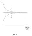
- FIG. 1schematically illustrates two types of common temperature profiles of a substrate processed in a RTP chamber.
- the vertical axisdenotes measured temperatures on a substrate.
- the horizontal axisdenotes the distance from the edge of the substrate.
- Profile 1is an edge high profile where the edge of the substrate has the highest temperature measurement.
- Profile 1is an edge low profile where the edge of the substrate has the lowest temperature measurement. It is difficult to remove temperature deviation near the edge of the substrate in the state of the art RTP systems.
- the present inventiongenerally provides apparatus and methods for achieving uniform heating to a substrate during a rapid thermal process.
- One embodiment of the present inventionprovides a chamber for processing a substrate comprising a chamber enclosure defining a processing volume, a substrate support disposed in the processing volume, an edge ring disposed on the substrate support, the edge ring is configured to support the substrate on a periphery of the substrate, a first heat source configured to heat the substrate, and a second heat source configured to heat the edge ring, wherein the second heat source is independently controllable from the first heat source.
- a rapid thermal processing chambercomprising a chamber body defining a chamber volume, a temperature controlled edge ring disposed in the chamber volume, wherein the temperature controlled edge ring is configured to thermally coupled with a substrate being processed near a periphery of the substrate, a first heat source configured for primarily heating a surface of the substrate, and a second heat source configured for primarily heating the temperature controlled edge ring.
- Yet another embodiment of the present inventionprovides a method for uniformly heating a substrate to a target temperature comprising positioning the substrate in a processing chamber connected with a first heat source, thermally coupling a periphery of the substrate to an edge ring, heating a surface of the substrate with the first heat source, and maintaining the edge ring at a ring temperature differs from the target temperature.
- FIG. 1schematically illustrates two types of common temperature profiles of a substrate processed in a RTP chamber.
- FIG. 2schematically illustrates a sectional view of a rapid thermal processing system in accordance with one embodiment of the present invention.
- FIG. 3schematically illustrates a sectional view of a rapid thermal processing system in accordance with another embodiment of the present invention.
- FIG. 4schematically illustrates a sectional view of an edge ring in accordance with one embodiment of the present invention.
- the present inventionprovides apparatus and methods for achieving uniform heating to a substrate during a rapid thermal process. More particularly, the present invention provides apparatus and methods for controlling the temperature of an edge ring supporting a substrate during a rapid thermal process to improve temperature uniformity across the substrate.
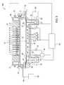
- FIG. 2schematically illustrates a sectional view of a rapid thermal processing system 10 in accordance with one embodiment of the present invention.
- the rapid thermal processing system 10comprises a chamber body 35 defining a processing volume 14 configured for annealing a disk-shaped substrate 12 therein.
- the chamber body 35may be made of stainless steel and may be lined with quartz.
- the processing volume 14is configured to be radiantly heated by a heating assembly 16 disposed on a quartz window 18 of the rapid thermal processing system 10 .
- the quartz window 18may be water cooled.
- a slit valve 30may be formed on a side of the chamber body 35 providing a passage for the substrate 12 to the processing volume 14 .
- a gas inlet 44may be connected to a gas source 45 to provide processing gases, purge gases and/or cleaning gases to the processing volume 14 .
- a vacuum pump 55may be fluidly connected to the processing volume 14 through an outlet 54 for pumping out the processing volume 14 .
- a circular channel 22is formed near the bottom of the chamber body 35 .
- a magnetic rotor 21is disposed in the circular channel 22 .
- a tubular riser 39rests on or otherwise coupled to the magnetic rotor 21 .
- the substrate 12is supported by a peripheral edge by an edge ring 20 disposed on the tubular riser 39 .
- a magnetic stator 23is located externally of the magnetic rotor 21 and is magnetically coupled through the chamber body 35 to induce rotation of the magnetic rotor 21 and hence of the edge ring 20 and the substrate 12 supported thereon.
- the magnetic stator 23may be also configured to adjust the elevations of the magnetic rotor 21 , thus lifting the substrate 12 being processed. Additional magnetic rotation and levitation information is available in the U.S. Pat. No. 6,800,833, which is hereby incorporated by reference.
- the chamber body 35may include a reflector plate 27 near the back side of the substrate 12 .
- the reflector plate 27has an optical reflective surface 28 facing the back side of the substrate 12 to enhance the emissivity of the substrate 12 .
- the reflector plate 27may be water cooled.
- the reflective surface 28 and the back side of the substrate 12define a reflective cavity 15 .
- the reflector plate 27has a diameter slightly larger than the diameter of the substrate 12 being processed. For example, if the rapid thermal processing system 10 is configured to process 12 inch substrates, the diameter of the reflector plate 27 may be about 13 inches.
- a purge gasmay be provided to the reflector plate 27 through a purge gas inlet 48 connected to a purge gas source 46 .
- the purge gas ejected to the reflector plate 27helps cooling of the reflector plate 27 especially near the apertures 25 where heat is not reflected back to the substrate 12 .
- an outer ring 19may be coupled between the chamber body 35 and the edge ring 20 to separate the reflective cavity 15 from the processing volume 14 .
- the reflective cavity 15 and the processing volume 14may have different environments.
- the heating assembly 16may comprise an array of heating elements 37 .
- the array of heating elements 37may be UV lamps, halogen lamps, laser diodes, resistive heaters, microwave powered heaters, light emitting diodes (LEDs), or any other suitable heating elements both singly or in combination.
- the array of heating elements 37may be disposed in vertical holes formed in a reflector body 53 . In one embodiment, the heating elements 37 may be arranged in a hexagon pattern.
- a cooling channel 40may be formed in the reflector body 53 .
- a coolant, such as water,may enter the reflector body 53 from an inlet 41 , travel adjacent the vertical holes cooling the array of heating elements 37 , and exit the reflector body from an exit 42 .
- the array of heating elements 37are connected to a controller 52 which are capable of adjusting heating effects of the array of heating elements 37 .
- the array of heating elements 37may be divided into a plurality of heating groups to heat the substrate 12 by multiple concentric zones. Each heating group may be controlled independently to provide desired temperature profile across a radius of the substrate 12 .
- Detailed descriptions of the heating assembly 16may be found in U.S. Pat. No. 6,350,964 and No. 6,927,169, which are hereby incorporated by reference.
- an edge ring heating assembly 38configured primarily to heat the edge ring 20 may be disposed outside the array of heating elements 37 .
- the edge ring heating assembly 38is connected to the controller 52 which may adjust the heating power of the edge ring heating assembly 38 .
- the edge ring heating assembly 38is independently controllable from the array of heating elements 37 , hence controlling the temperature of the edge ring 20 independently from the temperature of the substrate 12 .
- the edge ring heating assembly 38may be one of the heating groups of the array of heating elements 37 .
- the rapid thermal processing system 10further comprise a plurality of thermal probes 24 configured to measure thermal properties of the substrate 12 at different radial locations.
- the plurality of thermal probes 24may be a plurality of pyrometers optically coupled to and disposed in a plurality of apertures 25 formed in the reflector plate 27 to detect a temperature or other thermal properties of a different radial portion of the substrate 12 .
- the plurality of temperature probes 24is connected with the controller 52 which may conduct a closed loop control to adjust the power supplies to the array of heating elements 37 to provide a tailored radial thermal profile across the substrate 12 .
- the rapid thermal processing system 10further comprises an edge ring thermal probe 31 coupled to and disposed in an aperture 32 on the reflector plate 27 near the edge ring 20 .
- the edge ring thermal probe 31may be a pyrometer configured to measure a temperature or other thermal properties of the edge ring 20 .
- the edge ring thermal probe 31is connected with the controller 52 which is connected to the edge ring heating assembly 38 .
- the controller 52may conduct a closed loop control to the edge ring heating assembly 38 using the measurement from the edge ring thermal probe 31 .
- the edge ring 20may be heated to a desired temperature independently from the substrate 12 during a thermal process.
- a gas jet 47may be disposed near the edge ring 20 for cooling the edge ring 20 .
- the gas jet 47may share the same purge gas source 46 with the purge gas inlet 48 .
- the gas jet 47may be directed to the edge ring 20 and ejecting a cooling gas, such as helium, to cool the edge ring 20 .
- the gas jet 47may be connected to the gas source 46 through a valve 49 which may be controlled by the controller 52 .
- the controller 52therefore, may include the cooling effect of the gas jet 47 in the closed looped temperature control of the edge ring 20 .
- the edge ring 20may be designed to have thermal properties, such as thermal mass, emissivity and absorptivity, according to the thermal properties of the substrate 12 being processed to improve substrate temperature profile.
- the thermal properties of the edge ring 20may be altered by choosing different materials, different thicknesses and different coatings.
- a detailed description of edge ring designmay be found in the U.S. Pat. No. 7,127,367 (Attorney Docket No. 008504), which is hereby incorporated by reference.
- the edge ring 20may be made from silicon with a nickel coating.
- the substrate 12may be transferred to the processing volume 14 through the slit valve 30 and supported by the edge ring 20 .
- the magnetic rotor 21may rotate the substrate 12 and position the substrate 12 in a desired elevation.
- the objectiveis to rapidly heat the substrate 12 uniformly to a target temperature.
- heat transfer to the substrate 12mainly comes from radiation of the array of heating elements 37 and conduction and/or radiation from the edge ring 20 which is heated in a desired temperature.
- a uniform temperature profile across the substrate 12may be achieved by controlling the array of heating elements 37 and by keeping the edge ring 20 at the desired temperature which is usually different than the target temperature for the substrate 12 .
- Controlling the array of heating element 37may be conducted by measuring the temperature of the substrate 12 across a radius using the plurality of thermal probes 24 .
- the plurality of thermal probes 24may be evenly distributed across the reflector plate 27 corresponding to a radius of the substrate 12 .
- the measured temperatures from the plurality of thermal probes 24are sampled by the controller 52 .
- the controller 52may used the measured temperatures to adjust the array of heating elements 37 so that the temperature across a radius of the substrate 12 becoming uniform.
- the controller 52may adjust the array of heating elements 37 by a plurality of concentric zones. Detailed descriptions of controlling heating elements by multiple zones may be found in U.S. Pat. No. 5,755,511 and U.S. patent application Ser. No. 11/195,395, published as U.S. Patent Application Publication No. 2006/0066193 (Attorney Docket No. 009150), which are hereby incorporated by reference.
- heat exchange between the edge ring 20 and a periphery of the substrate 12is used to adjust the temperature profile near the edge of the substrate 12 .
- Heat exchangemay be achieved by conduction and/or radiation between the substrate 12 and the edge ring 20 .
- heat exchangemay be conducted by heating the edge ring 20 to a temperature different from the target temperature of the substrate 12 .
- a desired temperaturemay be predetermined for the edge ring 20 according to process requirements and thermal properties of both the edge ring 20 and the substrate 12 .
- the predetermined desired temperature of the edge ring 20may be about 10° C. to about 15° C. different from the target temperature of the substrate 12 .
- the predetermined desired temperature of the edge ring 20may be higher than the target temperature of the substrate 12 .
- the predetermined desired temperature of the edge ring 20may be lower than the target temperature of the substrate 12 .
- the desired edge ring temperaturemay be determined from either heat transfer modeling (conductive, radiative, convective) or from experimental results. In either case, the optical properties of the substrate and/or the edge ring are varied and the temperature uniformity of the wafer is measured. the results of these experiments lead to prediction of the desired temperature profile for the edge ring to achieve the best uniformity on the substrate.
- the desired temperature for the edge ring 20may be dynamic and adjustable according to the in-situ thermal measurements of the substrate 12 and the edge ring 20 .
- Heating the edge ring 20may be achieved primarily by using the edge ring heating assembly 38 .
- a closed loop controlmay be achieved by the controller 52 by adjusting the temperature of the edge ring 20 from the measurement of the edge ring thermal probe 31 .
- Adjustment of the temperature of the edge ring 20may be achieved by adjusting the power supply of the edge ring heating assembly 38 and/or flow rate of the cooling gas from the gas jet 47 .
- the edge ring 20may be over heated and then cooled down to a desired temperature with cooling gas from the gas jet 47 .
- the cooling gas for the gas jet 47may be used to cool the edge ring 20 to between about 100° C. and about 200° C. after processing one substrate and prior to the entry of the next substrate.
- the method of the present inventioncan provide less than 2° C., 3 sigma temperature uniformity for spike annealing.
- the method of the present inventionprovide less than 1° C., 3 sigma temperature uniformity for high temperature soak annealing up to 1350° C.
- the method of the present inventioncan heat a substrate at a temperature between about 200° C. to about 1350° C. with a temperature deviation of about 1° C. to about 1.5° C.
- the edge ring heating element 38 of the rapid thermal processing system 10is illustrated as a plurality of heating lamps.
- Other suitable heating devicesuch as for example solid state heaters (i.e., LEDs), laser heaters, inductive heaters, and microwave heaters, electrical heaters (e.g., resistive heating) can be used in the rapid thermal processing systems of the present invention.
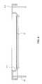
- FIG. 3schematically illustrates a sectional view of a rapid thermal processing system 100 having an edge ring heating element 51 positioned below the edge ring 20 .
- a substratemay be heated from a backside during thermal processing.
- An exemplary backside heating chambermay comprise an edge ring for supporting the substrate by a periphery with a frontside (the production side) facing up.
- An array of heating elementssimilar to the heating elements 37 , may be positioned underneath the edge ring so that the substrate can be heated from the backside.
- a plurality of probesmay be positioned across the radius of the substrate above the edge ring to measure a temperature profile of the substrate during thermal processing.
- An edge ring heater dedicated to independently heat the edge ringmay be positioned near the edge ring, underneath the edge ring, above the edge ring, or on a side of the edge ring.
- An edge ring probemay be positioned adjacent the edge ring configured to measure the temperature of the edge ring.
- a controllermay be connected to the edge ring heater, the edge ring probe, the array of heating elements and the plurality of probes to control the temperature profile of the substrate and the temperature of the edge ring in-situ.
- FIG. 4schematically illustrates a sectional view of an edge ring 110 in accordance with one embodiment of the present invention.
- the edge ring 110has a slant lip 111 configured to support the substrate 12 .
- the edge ring 110is designed to reduce the contact area with the substrate 12 . By reducing the contact area between the substrate 12 and the edge ring 110 , the heating condition near the edge of the substrate 12 may be simplified and edge high/low effect may be reduced. Additionally, reducing contact area also reduces particle contamination in the processing chamber.
Landscapes
- Engineering & Computer Science (AREA)
- Manufacturing & Machinery (AREA)
- Computer Hardware Design (AREA)
- Microelectronics & Electronic Packaging (AREA)
- Power Engineering (AREA)
- Physics & Mathematics (AREA)
- Condensed Matter Physics & Semiconductors (AREA)
- General Physics & Mathematics (AREA)
- Health & Medical Sciences (AREA)
- Toxicology (AREA)
- Chemical Vapour Deposition (AREA)
- Container, Conveyance, Adherence, Positioning, Of Wafer (AREA)
Abstract
Description
- Field of the Invention
- This application is a divisional application of co-pending U.S. patent application Ser. No. 11/623,238, filed Jan. 15, 2007, which is herein incorporated by reference.
- 1. Field of the Invention
- The present invention generally relates to the field of semiconductor processing. More particularly, the present invention relates to methods and apparatus for thermally processing a semiconductor substrate.
- 2. Description of the Related Art
- Rapid thermal processing (RTP) is a process for annealing substrates during semiconductor processing. During RTP, thermal radiation is generally used to rapidly heat a substrate in a controlled environment to a maximum temperature of up to about 1350° C. This maximum temperature is maintained for a specific amount of time ranging from less than one second to several minutes depending on the process. The substrate is then cooled to room temperature for further processing. High intensity tungsten halogen lamps are commonly used as the source of heat radiation. The substrate may be provided additional heat by a heated susceptor conductively coupled to the substrate.
- The semiconductor fabrication process has several applications of RTP. Such applications include thermal oxidation, high temperature soak anneal, low temperature soak anneal, and spike anneal. In thermal oxidation, a substrate is heated in oxygen, ozone, or a combination of oxygen and hydrogen which causes silicon substrate to oxidize to form silicon oxide. In high temperature soak anneal, a substrate is exposed to different gas mixtures such as nitrogen, ammonia, or oxygen. Low temperature soak anneal is generally used to anneal substrate deposited with metal. Spike anneal is used when the substrate needs to be exposed to high temperature for a very short time. During a spike anneal, the substrate is rapidly heated to a maximum temperature sufficient to activate dopant and cooled rapidly to end the activation process prior to substantial diffusion of the dopant.
- RTP usually requires a substantially uniform temperature profile across the substrate. In the state of the art process, the temperature uniformity may be improved by controlling heat sources, such as a laser, an array of lamps, configured to heat the substrate on the front side while a reflective surface on the back side reflects heat back to the substrate. Emissivity measurement and compensation methodology have been used to improve the temperature gradient across the substrate.
- As the semiconductor industry develops, the requirement for temperature uniformity during a RTP also increases. In some processes, it is important to have substantially small temperature gradient from about 2 mm inside the edge of the substrate. Particularly, it may be necessary to heat a substrate at a temperature between about 200° C. to about 1350° C. with a temperature deviation of about 1° C. to 1.5° C. The state of the art RTP systems have difficulties to reach this kind of uniformity, especially near the edge of the substrate. In a RTP system, an edge ring is usually used to support a substrate near the periphery. The edge ring and the substrate overlap producing a complicated heating situation near the edge of the substrate. In one aspect, the substrate may have different thermal properties near the edge. This is mostly pronounced for a patterned substrate, or for a silicon-on isulator—(SOI) substrate. In another aspect, the substrate and the edge ring overlap near the edge, it is difficult to achieve uniform temperature profile near the edge by measuring and adjusting the temperature of the substrate alone. Depending on the edge ring's thermal properties relative to the substrate's thermal and optical properties, the temperature profile of a substrate is generally either edge high or edge low.
FIG. 1 schematically illustrates two types of common temperature profiles of a substrate processed in a RTP chamber. The vertical axis denotes measured temperatures on a substrate. The horizontal axis denotes the distance from the edge of the substrate.Profile 1 is an edge high profile where the edge of the substrate has the highest temperature measurement.Profile 1 is an edge low profile where the edge of the substrate has the lowest temperature measurement. It is difficult to remove temperature deviation near the edge of the substrate in the state of the art RTP systems.- Therefore, there is a need for apparatus and methods used in RTP for improved temperature uniformity.
- The present invention generally provides apparatus and methods for achieving uniform heating to a substrate during a rapid thermal process.
- One embodiment of the present invention provides a chamber for processing a substrate comprising a chamber enclosure defining a processing volume, a substrate support disposed in the processing volume, an edge ring disposed on the substrate support, the edge ring is configured to support the substrate on a periphery of the substrate, a first heat source configured to heat the substrate, and a second heat source configured to heat the edge ring, wherein the second heat source is independently controllable from the first heat source.
- Another embodiment of the present invention provides a rapid thermal processing chamber comprising a chamber body defining a chamber volume, a temperature controlled edge ring disposed in the chamber volume, wherein the temperature controlled edge ring is configured to thermally coupled with a substrate being processed near a periphery of the substrate, a first heat source configured for primarily heating a surface of the substrate, and a second heat source configured for primarily heating the temperature controlled edge ring.
- Yet another embodiment of the present invention provides a method for uniformly heating a substrate to a target temperature comprising positioning the substrate in a processing chamber connected with a first heat source, thermally coupling a periphery of the substrate to an edge ring, heating a surface of the substrate with the first heat source, and maintaining the edge ring at a ring temperature differs from the target temperature.
- So that the manner in which the above recited features of the present invention can be understood in detail, a more particular description of the invention, briefly summarized above, may be had by reference to embodiments, some of which are illustrated in the appended drawings. It is to be noted, however, that the appended drawings illustrate only typical embodiments of this invention and are therefore not to be considered limiting of its scope, for the invention may admit to other equally effective embodiments.
FIG. 1 schematically illustrates two types of common temperature profiles of a substrate processed in a RTP chamber.FIG. 2 schematically illustrates a sectional view of a rapid thermal processing system in accordance with one embodiment of the present invention.FIG. 3 schematically illustrates a sectional view of a rapid thermal processing system in accordance with another embodiment of the present invention.FIG. 4 schematically illustrates a sectional view of an edge ring in accordance with one embodiment of the present invention.- The present invention provides apparatus and methods for achieving uniform heating to a substrate during a rapid thermal process. More particularly, the present invention provides apparatus and methods for controlling the temperature of an edge ring supporting a substrate during a rapid thermal process to improve temperature uniformity across the substrate.
FIG. 2 schematically illustrates a sectional view of a rapidthermal processing system 10 in accordance with one embodiment of the present invention. The rapidthermal processing system 10 comprises achamber body 35 defining aprocessing volume 14 configured for annealing a disk-shaped substrate 12 therein. Thechamber body 35 may be made of stainless steel and may be lined with quartz. Theprocessing volume 14 is configured to be radiantly heated by aheating assembly 16 disposed on aquartz window 18 of the rapidthermal processing system 10. In one embodiment, thequartz window 18 may be water cooled.- A
slit valve 30 may be formed on a side of thechamber body 35 providing a passage for thesubstrate 12 to theprocessing volume 14. Agas inlet 44 may be connected to agas source 45 to provide processing gases, purge gases and/or cleaning gases to theprocessing volume 14. Avacuum pump 55 may be fluidly connected to theprocessing volume 14 through anoutlet 54 for pumping out theprocessing volume 14. - A
circular channel 22 is formed near the bottom of thechamber body 35. Amagnetic rotor 21 is disposed in thecircular channel 22. Atubular riser 39 rests on or otherwise coupled to themagnetic rotor 21. Thesubstrate 12 is supported by a peripheral edge by anedge ring 20 disposed on thetubular riser 39. Amagnetic stator 23 is located externally of themagnetic rotor 21 and is magnetically coupled through thechamber body 35 to induce rotation of themagnetic rotor 21 and hence of theedge ring 20 and thesubstrate 12 supported thereon. Themagnetic stator 23 may be also configured to adjust the elevations of themagnetic rotor 21, thus lifting thesubstrate 12 being processed. Additional magnetic rotation and levitation information is available in the U.S. Pat. No. 6,800,833, which is hereby incorporated by reference. - The
chamber body 35 may include areflector plate 27 near the back side of thesubstrate 12. Thereflector plate 27 has an opticalreflective surface 28 facing the back side of thesubstrate 12 to enhance the emissivity of thesubstrate 12. In one embodiment, thereflector plate 27 may be water cooled. Thereflective surface 28 and the back side of thesubstrate 12 define areflective cavity 15. In one embodiment, thereflector plate 27 has a diameter slightly larger than the diameter of thesubstrate 12 being processed. For example, if the rapidthermal processing system 10 is configured to process 12 inch substrates, the diameter of thereflector plate 27 may be about 13 inches. - A purge gas may be provided to the
reflector plate 27 through apurge gas inlet 48 connected to apurge gas source 46. The purge gas ejected to thereflector plate 27 helps cooling of thereflector plate 27 especially near theapertures 25 where heat is not reflected back to thesubstrate 12. - In one embodiment, an
outer ring 19 may be coupled between thechamber body 35 and theedge ring 20 to separate thereflective cavity 15 from theprocessing volume 14. Thereflective cavity 15 and theprocessing volume 14 may have different environments. - The
heating assembly 16 may comprise an array ofheating elements 37. The array ofheating elements 37 may be UV lamps, halogen lamps, laser diodes, resistive heaters, microwave powered heaters, light emitting diodes (LEDs), or any other suitable heating elements both singly or in combination. The array ofheating elements 37 may be disposed in vertical holes formed in areflector body 53. In one embodiment, theheating elements 37 may be arranged in a hexagon pattern. A coolingchannel 40 may be formed in thereflector body 53. A coolant, such as water, may enter thereflector body 53 from aninlet 41, travel adjacent the vertical holes cooling the array ofheating elements 37, and exit the reflector body from anexit 42. - The array of
heating elements 37 are connected to acontroller 52 which are capable of adjusting heating effects of the array ofheating elements 37. In one embodiment, the array ofheating elements 37 may be divided into a plurality of heating groups to heat thesubstrate 12 by multiple concentric zones. Each heating group may be controlled independently to provide desired temperature profile across a radius of thesubstrate 12. Detailed descriptions of theheating assembly 16 may be found in U.S. Pat. No. 6,350,964 and No. 6,927,169, which are hereby incorporated by reference. - In one embodiment, an edge
ring heating assembly 38 configured primarily to heat theedge ring 20 may be disposed outside the array ofheating elements 37. The edgering heating assembly 38 is connected to thecontroller 52 which may adjust the heating power of the edgering heating assembly 38. The edgering heating assembly 38 is independently controllable from the array ofheating elements 37, hence controlling the temperature of theedge ring 20 independently from the temperature of thesubstrate 12. In one embodiment, the edgering heating assembly 38 may be one of the heating groups of the array ofheating elements 37. - The rapid
thermal processing system 10 further comprise a plurality ofthermal probes 24 configured to measure thermal properties of thesubstrate 12 at different radial locations. In one embodiment, the plurality ofthermal probes 24 may be a plurality of pyrometers optically coupled to and disposed in a plurality ofapertures 25 formed in thereflector plate 27 to detect a temperature or other thermal properties of a different radial portion of thesubstrate 12. Detailed description of similar temperature probes may be found in the U.S. Pat. No. 5,755,511, which is hereby incorporated by reference. The plurality of temperature probes24 is connected with thecontroller 52 which may conduct a closed loop control to adjust the power supplies to the array ofheating elements 37 to provide a tailored radial thermal profile across thesubstrate 12. - The rapid
thermal processing system 10 further comprises an edge ringthermal probe 31 coupled to and disposed in anaperture 32 on thereflector plate 27 near theedge ring 20. The edge ringthermal probe 31 may be a pyrometer configured to measure a temperature or other thermal properties of theedge ring 20. The edge ringthermal probe 31 is connected with thecontroller 52 which is connected to the edgering heating assembly 38. Thecontroller 52 may conduct a closed loop control to the edgering heating assembly 38 using the measurement from the edge ringthermal probe 31. In one embodiment, theedge ring 20 may be heated to a desired temperature independently from thesubstrate 12 during a thermal process. - A
gas jet 47 may be disposed near theedge ring 20 for cooling theedge ring 20. In one embodiment, thegas jet 47 may share the samepurge gas source 46 with thepurge gas inlet 48. Thegas jet 47 may be directed to theedge ring 20 and ejecting a cooling gas, such as helium, to cool theedge ring 20. Thegas jet 47 may be connected to thegas source 46 through avalve 49 which may be controlled by thecontroller 52. Thecontroller 52, therefore, may include the cooling effect of thegas jet 47 in the closed looped temperature control of theedge ring 20. - The
edge ring 20 may be designed to have thermal properties, such as thermal mass, emissivity and absorptivity, according to the thermal properties of thesubstrate 12 being processed to improve substrate temperature profile. The thermal properties of theedge ring 20 may be altered by choosing different materials, different thicknesses and different coatings. A detailed description of edge ring design may be found in the U.S. Pat. No. 7,127,367 (Attorney Docket No. 008504), which is hereby incorporated by reference. In one embodiment, theedge ring 20 may be made from silicon with a nickel coating. - During a rapid thermal process, the
substrate 12 may be transferred to theprocessing volume 14 through theslit valve 30 and supported by theedge ring 20. Themagnetic rotor 21 may rotate thesubstrate 12 and position thesubstrate 12 in a desired elevation. During most processes, the objective is to rapidly heat thesubstrate 12 uniformly to a target temperature. In one embodiment of the present invention, heat transfer to thesubstrate 12 mainly comes from radiation of the array ofheating elements 37 and conduction and/or radiation from theedge ring 20 which is heated in a desired temperature. A uniform temperature profile across thesubstrate 12 may be achieved by controlling the array ofheating elements 37 and by keeping theedge ring 20 at the desired temperature which is usually different than the target temperature for thesubstrate 12. - Controlling the array of
heating element 37 may be conducted by measuring the temperature of thesubstrate 12 across a radius using the plurality ofthermal probes 24. In one embodiment, the plurality ofthermal probes 24 may be evenly distributed across thereflector plate 27 corresponding to a radius of thesubstrate 12. The measured temperatures from the plurality ofthermal probes 24 are sampled by thecontroller 52. Thecontroller 52 may used the measured temperatures to adjust the array ofheating elements 37 so that the temperature across a radius of thesubstrate 12 becoming uniform. In one embodiment, thecontroller 52 may adjust the array ofheating elements 37 by a plurality of concentric zones. Detailed descriptions of controlling heating elements by multiple zones may be found in U.S. Pat. No. 5,755,511 and U.S. patent application Ser. No. 11/195,395, published as U.S. Patent Application Publication No. 2006/0066193 (Attorney Docket No. 009150), which are hereby incorporated by reference. - In one embodiment, heat exchange between the
edge ring 20 and a periphery of thesubstrate 12 is used to adjust the temperature profile near the edge of thesubstrate 12. Heat exchange may be achieved by conduction and/or radiation between thesubstrate 12 and theedge ring 20. In one embodiment, heat exchange may be conducted by heating theedge ring 20 to a temperature different from the target temperature of thesubstrate 12. - In one embodiment, a desired temperature may be predetermined for the
edge ring 20 according to process requirements and thermal properties of both theedge ring 20 and thesubstrate 12. In one embodiment, the predetermined desired temperature of theedge ring 20 may be about 10° C. to about 15° C. different from the target temperature of thesubstrate 12. In one embodiment, the predetermined desired temperature of theedge ring 20 may be higher than the target temperature of thesubstrate 12. In another embodiment, the predetermined desired temperature of theedge ring 20 may be lower than the target temperature of thesubstrate 12. The desired edge ring temperature may be determined from either heat transfer modeling (conductive, radiative, convective) or from experimental results. In either case, the optical properties of the substrate and/or the edge ring are varied and the temperature uniformity of the wafer is measured. the results of these experiments lead to prediction of the desired temperature profile for the edge ring to achieve the best uniformity on the substrate. - In another embodiment, the desired temperature for the
edge ring 20 may be dynamic and adjustable according to the in-situ thermal measurements of thesubstrate 12 and theedge ring 20. - Heating the
edge ring 20 may be achieved primarily by using the edgering heating assembly 38. A closed loop control may be achieved by thecontroller 52 by adjusting the temperature of theedge ring 20 from the measurement of the edge ringthermal probe 31. Adjustment of the temperature of theedge ring 20 may be achieved by adjusting the power supply of the edgering heating assembly 38 and/or flow rate of the cooling gas from thegas jet 47. In one embodiment, theedge ring 20 may be over heated and then cooled down to a desired temperature with cooling gas from thegas jet 47. - In one embodiment of the present invention, the cooling gas for the
gas jet 47 may be used to cool theedge ring 20 to between about 100° C. and about 200° C. after processing one substrate and prior to the entry of the next substrate. - The method of the present invention can provide less than 2° C., 3 sigma temperature uniformity for spike annealing. The method of the present invention provide less than 1° C., 3 sigma temperature uniformity for high temperature soak annealing up to 1350° C. In one embodiment, the method of the present invention can heat a substrate at a temperature between about 200° C. to about 1350° C. with a temperature deviation of about 1° C. to about 1.5° C.
- The edge
ring heating element 38 of the rapidthermal processing system 10 is illustrated as a plurality of heating lamps. Other suitable heating device, such as for example solid state heaters (i.e., LEDs), laser heaters, inductive heaters, and microwave heaters, electrical heaters (e.g., resistive heating) can be used in the rapid thermal processing systems of the present invention. - Additionally, the edge ring heating element may be positioned in other suitable locations, such as underneath the edge ring, on a side of the edge ring.
FIG. 3 schematically illustrates a sectional view of a rapidthermal processing system 100 having an edgering heating element 51 positioned below theedge ring 20. - In another embodiment, a substrate may be heated from a backside during thermal processing. An exemplary backside heating chamber may comprise an edge ring for supporting the substrate by a periphery with a frontside (the production side) facing up. An array of heating elements, similar to the
heating elements 37, may be positioned underneath the edge ring so that the substrate can be heated from the backside. A plurality of probes may be positioned across the radius of the substrate above the edge ring to measure a temperature profile of the substrate during thermal processing. An edge ring heater dedicated to independently heat the edge ring may be positioned near the edge ring, underneath the edge ring, above the edge ring, or on a side of the edge ring. An edge ring probe may be positioned adjacent the edge ring configured to measure the temperature of the edge ring. A controller may be connected to the edge ring heater, the edge ring probe, the array of heating elements and the plurality of probes to control the temperature profile of the substrate and the temperature of the edge ring in-situ. FIG. 4 schematically illustrates a sectional view of anedge ring 110 in accordance with one embodiment of the present invention. Theedge ring 110 has aslant lip 111 configured to support thesubstrate 12. Theedge ring 110 is designed to reduce the contact area with thesubstrate 12. By reducing the contact area between thesubstrate 12 and theedge ring 110, the heating condition near the edge of thesubstrate 12 may be simplified and edge high/low effect may be reduced. Additionally, reducing contact area also reduces particle contamination in the processing chamber.- Although the above discussion is focused on achieving uniform temperature profile across a substrate, a non-uniform temperature profile could also be achieved using the apparatus and methods of the present invention.
- While the foregoing is directed to embodiments of the present invention, other and further embodiments of the invention may be devised without departing from the basic scope thereof, and the scope thereof is determined by the claims that follow.
Claims (20)
1. A rapid thermal processing chamber, comprising:
a chamber body defining a chamber volume;
an edge ring to thermally couple to a substrate to be processed in the chamber, wherein the edge ring is disposed in the chamber volume;
a first heat source to heat a surface of the substrate; and
a second heat source to heat the edge ring.
2. The rapid thermal processing chamber ofclaim 1 , further comprising a thermal probe to measure at least one thermal property of the edge ring.
3. The rapid thermal processing chamber ofclaim 2 , further comprising a cooling device to reduce the temperature of the edge ring.
4. The rapid thermal processing chamber ofclaim 1 , wherein the first and second heat sources together comprise a lamp assembly to radiantly heat the chamber volume, and the lamp assembly has independently temperature controllable zones.
5. The rapid thermal processing chamber ofclaim 1 , wherein the first heat source and second heat source are disposed on opposite sides of the edge ring.
6. The rapid thermal processing chamber ofclaim 1 , wherein the second heat source is one of a radiant heater, a conductive heat source, a resistive heater, an inductive heater, and a microwave heater.
7. A method for uniformly heating a substrate to a target temperature, comprising:
positioning the substrate in a processing chamber, wherein the processing chamber is connected with a first heat source;
thermally coupling a periphery of the substrate to an edge ring;
heating a surface of the substrate with the first heat source; and
maintaining the edge ring at a first temperature, wherein the first temperature differs from the target temperature.
8. The method ofclaim 7 , further wherein maintaining the edge ring at the first temperature comprising heating the edge ring with a second heat source, wherein the first and second heat sources are independently controllable.
9. The method ofclaim 8 , wherein the first and second heat sources together comprise a lamp assembly having independently controllable zones.
10. The method ofclaim 8 , further comprising cooling the edge ring using a purge gas.
11. The method ofclaim 8 , further comprising:
measuring a temperature of the edge ring using a thermal probe to determine a measured temperature; and
adjusting the second heat source according to the measured temperature.
12. The method ofclaim 7 , wherein the first temperature differs from the target temperature for about 10° C. to about 15° C.
13. The method ofclaim 7 , wherein the first temperature is higher than the target temperature.
14. The method ofclaim 7 , wherein the first temperature is lower than the target temperature.
15. A rapid thermal processing chamber, comprising:
a chamber body defining a processing volume;
a substrate support mechanism disposed in the processing volume;
an edge ring disposed on the substrate support mechanism, wherein the edge ring supports a substrate being processed by a peripheral edge of the substrate, and heat exchange between the edge ring and the peripheral edge of the substrate adjusts a temperature profile of the substrate near the peripheral edge;
a first heat source to rapidly heat the substrate disposed on the edge ring; and
a second heat source to heat the edge ring at a temperature different from a temperature of the substrate.
16. The rapid thermal processing chamber ofclaim 15 , wherein the first heat source comprises an array of heating elements.
17. The rapid thermal processing chamber ofclaim 16 , wherein the first heat source and the second heat source are disposed on opposite sides of the substrate.
18. The rapid thermal processing chamber ofclaim 17 , wherein the second heat source comprises one or more laser heaters.
19. The rapid thermal processing chamber ofclaim 16 , wherein the array of heating elements are lamps disposed outside the chamber body and configured to provide thermal energy through a quartz window of the chamber body, and the second heat source comprises a plurality of lamps disposed radially outwards of the first heat source.
20. The rapid thermal processing chamber ofclaim 15 , further comprising:
a cooling device to reduce to temperature of the edge ring.
Priority Applications (1)
| Application Number | Priority Date | Filing Date | Title |
|---|---|---|---|
| US12/973,112US20110089166A1 (en) | 2007-01-15 | 2010-12-20 | Temperature measurement and control of wafer support in thermal processing chamber |
Applications Claiming Priority (2)
| Application Number | Priority Date | Filing Date | Title |
|---|---|---|---|
| US11/623,238US7860379B2 (en) | 2007-01-15 | 2007-01-15 | Temperature measurement and control of wafer support in thermal processing chamber |
| US12/973,112US20110089166A1 (en) | 2007-01-15 | 2010-12-20 | Temperature measurement and control of wafer support in thermal processing chamber |
Related Parent Applications (1)
| Application Number | Title | Priority Date | Filing Date |
|---|---|---|---|
| US11/623,238DivisionUS7860379B2 (en) | 2007-01-15 | 2007-01-15 | Temperature measurement and control of wafer support in thermal processing chamber |
Publications (1)
| Publication Number | Publication Date |
|---|---|
| US20110089166A1true US20110089166A1 (en) | 2011-04-21 |
Family
ID=39231046
Family Applications (2)
| Application Number | Title | Priority Date | Filing Date |
|---|---|---|---|
| US11/623,238Active2028-09-24US7860379B2 (en) | 2007-01-15 | 2007-01-15 | Temperature measurement and control of wafer support in thermal processing chamber |
| US12/973,112AbandonedUS20110089166A1 (en) | 2007-01-15 | 2010-12-20 | Temperature measurement and control of wafer support in thermal processing chamber |
Family Applications Before (1)
| Application Number | Title | Priority Date | Filing Date |
|---|---|---|---|
| US11/623,238Active2028-09-24US7860379B2 (en) | 2007-01-15 | 2007-01-15 | Temperature measurement and control of wafer support in thermal processing chamber |
Country Status (6)
| Country | Link |
|---|---|
| US (2) | US7860379B2 (en) |
| EP (1) | EP1944793A3 (en) |
| JP (1) | JP2008182228A (en) |
| KR (1) | KR100978975B1 (en) |
| CN (1) | CN101231941A (en) |
| TW (1) | TWI380372B (en) |
Cited By (329)
| Publication number | Priority date | Publication date | Assignee | Title |
|---|---|---|---|---|
| US20110147356A1 (en)* | 2009-12-23 | 2011-06-23 | Darrin Leonhardt | Uv led based lamp for compact uv curing lamp assemblies |
| US20120063752A1 (en)* | 2010-05-07 | 2012-03-15 | Cochran Don W | Corner-cube irradiation control |
| US20130206362A1 (en)* | 2012-02-09 | 2013-08-15 | Applied Materials, Inc. | Spike anneal residence time reduction in rapid thermal processing chambers |
| US20130323936A1 (en)* | 2012-05-30 | 2013-12-05 | Lawrence Livermore National Security, Llc | Apparatus and methods for rapid thermal processing |
| US9922889B2 (en) | 2015-11-04 | 2018-03-20 | SCREEN Holdings Co., Ltd. | Thermal processing method and thermal processing apparatus through light irradiation |
| US10202707B2 (en) | 2012-04-26 | 2019-02-12 | Applied Materials, Inc. | Substrate processing system with lamphead having temperature management |
| TWI669410B (en)* | 2014-05-07 | 2019-08-21 | 日商東京威力科創股份有限公司 | Film formation method and film formation device |
| US10559458B1 (en) | 2018-11-26 | 2020-02-11 | Asm Ip Holding B.V. | Method of forming oxynitride film |
| US10561975B2 (en) | 2014-10-07 | 2020-02-18 | Asm Ip Holdings B.V. | Variable conductance gas distribution apparatus and method |
| USD876504S1 (en) | 2017-04-03 | 2020-02-25 | Asm Ip Holding B.V. | Exhaust flow control ring for semiconductor deposition apparatus |
| US10590535B2 (en) | 2017-07-26 | 2020-03-17 | Asm Ip Holdings B.V. | Chemical treatment, deposition and/or infiltration apparatus and method for using the same |
| US10600673B2 (en) | 2015-07-07 | 2020-03-24 | Asm Ip Holding B.V. | Magnetic susceptor to baseplate seal |
| US10604847B2 (en) | 2014-03-18 | 2020-03-31 | Asm Ip Holding B.V. | Gas distribution system, reactor including the system, and methods of using the same |
| US10612136B2 (en) | 2018-06-29 | 2020-04-07 | ASM IP Holding, B.V. | Temperature-controlled flange and reactor system including same |
| US10622375B2 (en) | 2016-11-07 | 2020-04-14 | Asm Ip Holding B.V. | Method of processing a substrate and a device manufactured by using the method |
| US10643904B2 (en) | 2016-11-01 | 2020-05-05 | Asm Ip Holdings B.V. | Methods for forming a semiconductor device and related semiconductor device structures |
| US10643826B2 (en) | 2016-10-26 | 2020-05-05 | Asm Ip Holdings B.V. | Methods for thermally calibrating reaction chambers |
| US10658205B2 (en) | 2017-09-28 | 2020-05-19 | Asm Ip Holdings B.V. | Chemical dispensing apparatus and methods for dispensing a chemical to a reaction chamber |
| US10655221B2 (en) | 2017-02-09 | 2020-05-19 | Asm Ip Holding B.V. | Method for depositing oxide film by thermal ALD and PEALD |
| US10658181B2 (en) | 2018-02-20 | 2020-05-19 | Asm Ip Holding B.V. | Method of spacer-defined direct patterning in semiconductor fabrication |
| US10665452B2 (en) | 2016-05-02 | 2020-05-26 | Asm Ip Holdings B.V. | Source/drain performance through conformal solid state doping |
| US10672636B2 (en) | 2017-08-09 | 2020-06-02 | Asm Ip Holding B.V. | Cassette holder assembly for a substrate cassette and holding member for use in such assembly |
| US10685834B2 (en) | 2017-07-05 | 2020-06-16 | Asm Ip Holdings B.V. | Methods for forming a silicon germanium tin layer and related semiconductor device structures |
| US10683571B2 (en) | 2014-02-25 | 2020-06-16 | Asm Ip Holding B.V. | Gas supply manifold and method of supplying gases to chamber using same |
| US10692741B2 (en) | 2017-08-08 | 2020-06-23 | Asm Ip Holdings B.V. | Radiation shield |
| US10707106B2 (en) | 2011-06-06 | 2020-07-07 | Asm Ip Holding B.V. | High-throughput semiconductor-processing apparatus equipped with multiple dual-chamber modules |
| US10714315B2 (en) | 2012-10-12 | 2020-07-14 | Asm Ip Holdings B.V. | Semiconductor reaction chamber showerhead |
| US10714350B2 (en) | 2016-11-01 | 2020-07-14 | ASM IP Holdings, B.V. | Methods for forming a transition metal niobium nitride film on a substrate by atomic layer deposition and related semiconductor device structures |
| US10714385B2 (en) | 2016-07-19 | 2020-07-14 | Asm Ip Holding B.V. | Selective deposition of tungsten |
| US10714335B2 (en) | 2017-04-25 | 2020-07-14 | Asm Ip Holding B.V. | Method of depositing thin film and method of manufacturing semiconductor device |
| TWI699853B (en)* | 2017-05-30 | 2020-07-21 | 荷蘭商Asm知識產權私人控股有限公司 | Substrate supporting device, substrate processing apparatus and substrate processing method for film deposition |
| US10720322B2 (en) | 2016-02-19 | 2020-07-21 | Asm Ip Holding B.V. | Method for forming silicon nitride film selectively on top surface |
| US10720331B2 (en) | 2016-11-01 | 2020-07-21 | ASM IP Holdings, B.V. | Methods for forming a transition metal nitride film on a substrate by atomic layer deposition and related semiconductor device structures |
| US10734223B2 (en) | 2017-10-10 | 2020-08-04 | Asm Ip Holding B.V. | Method for depositing a metal chalcogenide on a substrate by cyclical deposition |
| US10734497B2 (en) | 2017-07-18 | 2020-08-04 | Asm Ip Holding B.V. | Methods for forming a semiconductor device structure and related semiconductor device structures |
| US10731249B2 (en) | 2018-02-15 | 2020-08-04 | Asm Ip Holding B.V. | Method of forming a transition metal containing film on a substrate by a cyclical deposition process, a method for supplying a transition metal halide compound to a reaction chamber, and related vapor deposition apparatus |
| US10734244B2 (en) | 2017-11-16 | 2020-08-04 | Asm Ip Holding B.V. | Method of processing a substrate and a device manufactured by the same |
| US10741385B2 (en) | 2016-07-28 | 2020-08-11 | Asm Ip Holding B.V. | Method and apparatus for filling a gap |
| US10755923B2 (en) | 2018-07-03 | 2020-08-25 | Asm Ip Holding B.V. | Method for depositing silicon-free carbon-containing film as gap-fill layer by pulse plasma-assisted deposition |
| US10755922B2 (en) | 2018-07-03 | 2020-08-25 | Asm Ip Holding B.V. | Method for depositing silicon-free carbon-containing film as gap-fill layer by pulse plasma-assisted deposition |
| US10770336B2 (en) | 2017-08-08 | 2020-09-08 | Asm Ip Holding B.V. | Substrate lift mechanism and reactor including same |
| US10767789B2 (en) | 2018-07-16 | 2020-09-08 | Asm Ip Holding B.V. | Diaphragm valves, valve components, and methods for forming valve components |
| US10770286B2 (en) | 2017-05-08 | 2020-09-08 | Asm Ip Holdings B.V. | Methods for selectively forming a silicon nitride film on a substrate and related semiconductor device structures |
| US10784102B2 (en) | 2016-12-22 | 2020-09-22 | Asm Ip Holding B.V. | Method of forming a structure on a substrate |
| US10787741B2 (en) | 2014-08-21 | 2020-09-29 | Asm Ip Holding B.V. | Method and system for in situ formation of gas-phase compounds |
| US10797133B2 (en) | 2018-06-21 | 2020-10-06 | Asm Ip Holding B.V. | Method for depositing a phosphorus doped silicon arsenide film and related semiconductor device structures |
| US10804098B2 (en) | 2009-08-14 | 2020-10-13 | Asm Ip Holding B.V. | Systems and methods for thin-film deposition of metal oxides using excited nitrogen-oxygen species |
| US10811256B2 (en) | 2018-10-16 | 2020-10-20 | Asm Ip Holding B.V. | Method for etching a carbon-containing feature |
| US10818758B2 (en) | 2018-11-16 | 2020-10-27 | Asm Ip Holding B.V. | Methods for forming a metal silicate film on a substrate in a reaction chamber and related semiconductor device structures |
| USD900036S1 (en) | 2017-08-24 | 2020-10-27 | Asm Ip Holding B.V. | Heater electrical connector and adapter |
| US10832903B2 (en) | 2011-10-28 | 2020-11-10 | Asm Ip Holding B.V. | Process feed management for semiconductor substrate processing |
| US10829852B2 (en) | 2018-08-16 | 2020-11-10 | Asm Ip Holding B.V. | Gas distribution device for a wafer processing apparatus |
| US10847371B2 (en) | 2018-03-27 | 2020-11-24 | Asm Ip Holding B.V. | Method of forming an electrode on a substrate and a semiconductor device structure including an electrode |
| US10844484B2 (en) | 2017-09-22 | 2020-11-24 | Asm Ip Holding B.V. | Apparatus for dispensing a vapor phase reactant to a reaction chamber and related methods |
| US10844486B2 (en) | 2009-04-06 | 2020-11-24 | Asm Ip Holding B.V. | Semiconductor processing reactor and components thereof |
| US10847366B2 (en) | 2018-11-16 | 2020-11-24 | Asm Ip Holding B.V. | Methods for depositing a transition metal chalcogenide film on a substrate by a cyclical deposition process |
| US10847365B2 (en) | 2018-10-11 | 2020-11-24 | Asm Ip Holding B.V. | Method of forming conformal silicon carbide film by cyclic CVD |
| US10854498B2 (en) | 2011-07-15 | 2020-12-01 | Asm Ip Holding B.V. | Wafer-supporting device and method for producing same |
| USD903477S1 (en) | 2018-01-24 | 2020-12-01 | Asm Ip Holdings B.V. | Metal clamp |
| US10851456B2 (en) | 2016-04-21 | 2020-12-01 | Asm Ip Holding B.V. | Deposition of metal borides |
| US10858737B2 (en) | 2014-07-28 | 2020-12-08 | Asm Ip Holding B.V. | Showerhead assembly and components thereof |
| US10867786B2 (en) | 2018-03-30 | 2020-12-15 | Asm Ip Holding B.V. | Substrate processing method |
| US10865475B2 (en) | 2016-04-21 | 2020-12-15 | Asm Ip Holding B.V. | Deposition of metal borides and silicides |
| US10867788B2 (en) | 2016-12-28 | 2020-12-15 | Asm Ip Holding B.V. | Method of forming a structure on a substrate |
| US10872771B2 (en) | 2018-01-16 | 2020-12-22 | Asm Ip Holding B. V. | Method for depositing a material film on a substrate within a reaction chamber by a cyclical deposition process and related device structures |
| US10883175B2 (en) | 2018-08-09 | 2021-01-05 | Asm Ip Holding B.V. | Vertical furnace for processing substrates and a liner for use therein |
| US10892156B2 (en) | 2017-05-08 | 2021-01-12 | Asm Ip Holding B.V. | Methods for forming a silicon nitride film on a substrate and related semiconductor device structures |
| US10896820B2 (en) | 2018-02-14 | 2021-01-19 | Asm Ip Holding B.V. | Method for depositing a ruthenium-containing film on a substrate by a cyclical deposition process |
| US10910262B2 (en) | 2017-11-16 | 2021-02-02 | Asm Ip Holding B.V. | Method of selectively depositing a capping layer structure on a semiconductor device structure |
| US10914004B2 (en) | 2018-06-29 | 2021-02-09 | Asm Ip Holding B.V. | Thin-film deposition method and manufacturing method of semiconductor device |
| US10923344B2 (en) | 2017-10-30 | 2021-02-16 | Asm Ip Holding B.V. | Methods for forming a semiconductor structure and related semiconductor structures |
| US10928731B2 (en) | 2017-09-21 | 2021-02-23 | Asm Ip Holding B.V. | Method of sequential infiltration synthesis treatment of infiltrateable material and structures and devices formed using same |
| US10934619B2 (en) | 2016-11-15 | 2021-03-02 | Asm Ip Holding B.V. | Gas supply unit and substrate processing apparatus including the gas supply unit |
| US10941490B2 (en) | 2014-10-07 | 2021-03-09 | Asm Ip Holding B.V. | Multiple temperature range susceptor, assembly, reactor and system including the susceptor, and methods of using the same |
| USD913980S1 (en) | 2018-02-01 | 2021-03-23 | Asm Ip Holding B.V. | Gas supply plate for semiconductor manufacturing apparatus |
| US10975470B2 (en) | 2018-02-23 | 2021-04-13 | Asm Ip Holding B.V. | Apparatus for detecting or monitoring for a chemical precursor in a high temperature environment |
| US11001925B2 (en) | 2016-12-19 | 2021-05-11 | Asm Ip Holding B.V. | Substrate processing apparatus |
| US11004977B2 (en) | 2017-07-19 | 2021-05-11 | Asm Ip Holding B.V. | Method for depositing a group IV semiconductor and related semiconductor device structures |
| US11018002B2 (en) | 2017-07-19 | 2021-05-25 | Asm Ip Holding B.V. | Method for selectively depositing a Group IV semiconductor and related semiconductor device structures |
| US11015245B2 (en) | 2014-03-19 | 2021-05-25 | Asm Ip Holding B.V. | Gas-phase reactor and system having exhaust plenum and components thereof |
| US11018047B2 (en) | 2018-01-25 | 2021-05-25 | Asm Ip Holding B.V. | Hybrid lift pin |
| US11022879B2 (en) | 2017-11-24 | 2021-06-01 | Asm Ip Holding B.V. | Method of forming an enhanced unexposed photoresist layer |
| US11024523B2 (en) | 2018-09-11 | 2021-06-01 | Asm Ip Holding B.V. | Substrate processing apparatus and method |
| US11031242B2 (en) | 2018-11-07 | 2021-06-08 | Asm Ip Holding B.V. | Methods for depositing a boron doped silicon germanium film |
| USD922229S1 (en) | 2019-06-05 | 2021-06-15 | Asm Ip Holding B.V. | Device for controlling a temperature of a gas supply unit |
| US11049751B2 (en) | 2018-09-14 | 2021-06-29 | Asm Ip Holding B.V. | Cassette supply system to store and handle cassettes and processing apparatus equipped therewith |
| US11053591B2 (en) | 2018-08-06 | 2021-07-06 | Asm Ip Holding B.V. | Multi-port gas injection system and reactor system including same |
| US11056567B2 (en) | 2018-05-11 | 2021-07-06 | Asm Ip Holding B.V. | Method of forming a doped metal carbide film on a substrate and related semiconductor device structures |
| US11056344B2 (en) | 2017-08-30 | 2021-07-06 | Asm Ip Holding B.V. | Layer forming method |
| US11069510B2 (en) | 2017-08-30 | 2021-07-20 | Asm Ip Holding B.V. | Substrate processing apparatus |
| US11081345B2 (en) | 2018-02-06 | 2021-08-03 | Asm Ip Holding B.V. | Method of post-deposition treatment for silicon oxide film |
| US11088002B2 (en) | 2018-03-29 | 2021-08-10 | Asm Ip Holding B.V. | Substrate rack and a substrate processing system and method |
| US11087997B2 (en) | 2018-10-31 | 2021-08-10 | Asm Ip Holding B.V. | Substrate processing apparatus for processing substrates |
| US11094582B2 (en) | 2016-07-08 | 2021-08-17 | Asm Ip Holding B.V. | Selective deposition method to form air gaps |
| US11094546B2 (en) | 2017-10-05 | 2021-08-17 | Asm Ip Holding B.V. | Method for selectively depositing a metallic film on a substrate |
| US11101370B2 (en) | 2016-05-02 | 2021-08-24 | Asm Ip Holding B.V. | Method of forming a germanium oxynitride film |
| US11114294B2 (en) | 2019-03-08 | 2021-09-07 | Asm Ip Holding B.V. | Structure including SiOC layer and method of forming same |
| US11114283B2 (en) | 2018-03-16 | 2021-09-07 | Asm Ip Holding B.V. | Reactor, system including the reactor, and methods of manufacturing and using same |
| USD930782S1 (en) | 2019-08-22 | 2021-09-14 | Asm Ip Holding B.V. | Gas distributor |
| US11127589B2 (en) | 2019-02-01 | 2021-09-21 | Asm Ip Holding B.V. | Method of topology-selective film formation of silicon oxide |
| US11127617B2 (en) | 2017-11-27 | 2021-09-21 | Asm Ip Holding B.V. | Storage device for storing wafer cassettes for use with a batch furnace |
| USD931978S1 (en) | 2019-06-27 | 2021-09-28 | Asm Ip Holding B.V. | Showerhead vacuum transport |
| US11139308B2 (en) | 2015-12-29 | 2021-10-05 | Asm Ip Holding B.V. | Atomic layer deposition of III-V compounds to form V-NAND devices |
| US11139191B2 (en) | 2017-08-09 | 2021-10-05 | Asm Ip Holding B.V. | Storage apparatus for storing cassettes for substrates and processing apparatus equipped therewith |
| US11158513B2 (en) | 2018-12-13 | 2021-10-26 | Asm Ip Holding B.V. | Methods for forming a rhenium-containing film on a substrate by a cyclical deposition process and related semiconductor device structures |
| US11171025B2 (en) | 2019-01-22 | 2021-11-09 | Asm Ip Holding B.V. | Substrate processing device |
| USD935572S1 (en) | 2019-05-24 | 2021-11-09 | Asm Ip Holding B.V. | Gas channel plate |
| WO2021247148A1 (en)* | 2020-06-03 | 2021-12-09 | Applied Materials, Inc. | Substrate processing system |
| US11205585B2 (en) | 2016-07-28 | 2021-12-21 | Asm Ip Holding B.V. | Substrate processing apparatus and method of operating the same |
| US11217444B2 (en) | 2018-11-30 | 2022-01-04 | Asm Ip Holding B.V. | Method for forming an ultraviolet radiation responsive metal oxide-containing film |
| US11222772B2 (en) | 2016-12-14 | 2022-01-11 | Asm Ip Holding B.V. | Substrate processing apparatus |
| USD940837S1 (en) | 2019-08-22 | 2022-01-11 | Asm Ip Holding B.V. | Electrode |
| US11227782B2 (en) | 2019-07-31 | 2022-01-18 | Asm Ip Holding B.V. | Vertical batch furnace assembly |
| US11227789B2 (en) | 2019-02-20 | 2022-01-18 | Asm Ip Holding B.V. | Method and apparatus for filling a recess formed within a substrate surface |
| US11232963B2 (en) | 2018-10-03 | 2022-01-25 | Asm Ip Holding B.V. | Substrate processing apparatus and method |
| US11233133B2 (en) | 2015-10-21 | 2022-01-25 | Asm Ip Holding B.V. | NbMC layers |
| US11230766B2 (en) | 2018-03-29 | 2022-01-25 | Asm Ip Holding B.V. | Substrate processing apparatus and method |
| US11242598B2 (en) | 2015-06-26 | 2022-02-08 | Asm Ip Holding B.V. | Structures including metal carbide material, devices including the structures, and methods of forming same |
| US11251068B2 (en) | 2018-10-19 | 2022-02-15 | Asm Ip Holding B.V. | Substrate processing apparatus and substrate processing method |
| US11251040B2 (en) | 2019-02-20 | 2022-02-15 | Asm Ip Holding B.V. | Cyclical deposition method including treatment step and apparatus for same |
| USD944946S1 (en) | 2019-06-14 | 2022-03-01 | Asm Ip Holding B.V. | Shower plate |
| US11270899B2 (en) | 2018-06-04 | 2022-03-08 | Asm Ip Holding B.V. | Wafer handling chamber with moisture reduction |
| US11274369B2 (en) | 2018-09-11 | 2022-03-15 | Asm Ip Holding B.V. | Thin film deposition method |
| US11282698B2 (en) | 2019-07-19 | 2022-03-22 | Asm Ip Holding B.V. | Method of forming topology-controlled amorphous carbon polymer film |
| US11289326B2 (en) | 2019-05-07 | 2022-03-29 | Asm Ip Holding B.V. | Method for reforming amorphous carbon polymer film |
| US11286558B2 (en) | 2019-08-23 | 2022-03-29 | Asm Ip Holding B.V. | Methods for depositing a molybdenum nitride film on a surface of a substrate by a cyclical deposition process and related semiconductor device structures including a molybdenum nitride film |
| US11286562B2 (en) | 2018-06-08 | 2022-03-29 | Asm Ip Holding B.V. | Gas-phase chemical reactor and method of using same |
| US11295980B2 (en) | 2017-08-30 | 2022-04-05 | Asm Ip Holding B.V. | Methods for depositing a molybdenum metal film over a dielectric surface of a substrate by a cyclical deposition process and related semiconductor device structures |
| USD947913S1 (en) | 2019-05-17 | 2022-04-05 | Asm Ip Holding B.V. | Susceptor shaft |
| USD948463S1 (en) | 2018-10-24 | 2022-04-12 | Asm Ip Holding B.V. | Susceptor for semiconductor substrate supporting apparatus |
| US11306395B2 (en) | 2017-06-28 | 2022-04-19 | Asm Ip Holding B.V. | Methods for depositing a transition metal nitride film on a substrate by atomic layer deposition and related deposition apparatus |
| USD949319S1 (en) | 2019-08-22 | 2022-04-19 | Asm Ip Holding B.V. | Exhaust duct |
| US11315794B2 (en) | 2019-10-21 | 2022-04-26 | Asm Ip Holding B.V. | Apparatus and methods for selectively etching films |
| US11342216B2 (en) | 2019-02-20 | 2022-05-24 | Asm Ip Holding B.V. | Cyclical deposition method and apparatus for filling a recess formed within a substrate surface |
| US11339476B2 (en) | 2019-10-08 | 2022-05-24 | Asm Ip Holding B.V. | Substrate processing device having connection plates, substrate processing method |
| US11345999B2 (en) | 2019-06-06 | 2022-05-31 | Asm Ip Holding B.V. | Method of using a gas-phase reactor system including analyzing exhausted gas |
| US11355338B2 (en) | 2019-05-10 | 2022-06-07 | Asm Ip Holding B.V. | Method of depositing material onto a surface and structure formed according to the method |
| US11361990B2 (en) | 2018-05-28 | 2022-06-14 | Asm Ip Holding B.V. | Substrate processing method and device manufactured by using the same |
| US11374112B2 (en) | 2017-07-19 | 2022-06-28 | Asm Ip Holding B.V. | Method for depositing a group IV semiconductor and related semiconductor device structures |
| US11378337B2 (en) | 2019-03-28 | 2022-07-05 | Asm Ip Holding B.V. | Door opener and substrate processing apparatus provided therewith |
| US11390950B2 (en) | 2017-01-10 | 2022-07-19 | Asm Ip Holding B.V. | Reactor system and method to reduce residue buildup during a film deposition process |
| US11390946B2 (en) | 2019-01-17 | 2022-07-19 | Asm Ip Holding B.V. | Methods of forming a transition metal containing film on a substrate by a cyclical deposition process |
| US11390945B2 (en) | 2019-07-03 | 2022-07-19 | Asm Ip Holding B.V. | Temperature control assembly for substrate processing apparatus and method of using same |
| US11393690B2 (en) | 2018-01-19 | 2022-07-19 | Asm Ip Holding B.V. | Deposition method |
| US11401605B2 (en) | 2019-11-26 | 2022-08-02 | Asm Ip Holding B.V. | Substrate processing apparatus |
| US11410851B2 (en) | 2017-02-15 | 2022-08-09 | Asm Ip Holding B.V. | Methods for forming a metallic film on a substrate by cyclical deposition and related semiconductor device structures |
| US11414760B2 (en) | 2018-10-08 | 2022-08-16 | Asm Ip Holding B.V. | Substrate support unit, thin film deposition apparatus including the same, and substrate processing apparatus including the same |
| US11424119B2 (en) | 2019-03-08 | 2022-08-23 | Asm Ip Holding B.V. | Method for selective deposition of silicon nitride layer and structure including selectively-deposited silicon nitride layer |
| US11430640B2 (en) | 2019-07-30 | 2022-08-30 | Asm Ip Holding B.V. | Substrate processing apparatus |
| US11430674B2 (en) | 2018-08-22 | 2022-08-30 | Asm Ip Holding B.V. | Sensor array, apparatus for dispensing a vapor phase reactant to a reaction chamber and related methods |
| US11437241B2 (en) | 2020-04-08 | 2022-09-06 | Asm Ip Holding B.V. | Apparatus and methods for selectively etching silicon oxide films |
| US11443926B2 (en) | 2019-07-30 | 2022-09-13 | Asm Ip Holding B.V. | Substrate processing apparatus |
| US11447864B2 (en) | 2019-04-19 | 2022-09-20 | Asm Ip Holding B.V. | Layer forming method and apparatus |
| US11447861B2 (en) | 2016-12-15 | 2022-09-20 | Asm Ip Holding B.V. | Sequential infiltration synthesis apparatus and a method of forming a patterned structure |
| USD965044S1 (en) | 2019-08-19 | 2022-09-27 | Asm Ip Holding B.V. | Susceptor shaft |
| US11453943B2 (en) | 2016-05-25 | 2022-09-27 | Asm Ip Holding B.V. | Method for forming carbon-containing silicon/metal oxide or nitride film by ALD using silicon precursor and hydrocarbon precursor |
| USD965524S1 (en) | 2019-08-19 | 2022-10-04 | Asm Ip Holding B.V. | Susceptor support |
| US11469098B2 (en) | 2018-05-08 | 2022-10-11 | Asm Ip Holding B.V. | Methods for depositing an oxide film on a substrate by a cyclical deposition process and related device structures |
| US11476109B2 (en) | 2019-06-11 | 2022-10-18 | Asm Ip Holding B.V. | Method of forming an electronic structure using reforming gas, system for performing the method, and structure formed using the method |
| US11473195B2 (en) | 2018-03-01 | 2022-10-18 | Asm Ip Holding B.V. | Semiconductor processing apparatus and a method for processing a substrate |
| US11482412B2 (en) | 2018-01-19 | 2022-10-25 | Asm Ip Holding B.V. | Method for depositing a gap-fill layer by plasma-assisted deposition |
| US11482533B2 (en) | 2019-02-20 | 2022-10-25 | Asm Ip Holding B.V. | Apparatus and methods for plug fill deposition in 3-D NAND applications |
| US11482418B2 (en) | 2018-02-20 | 2022-10-25 | Asm Ip Holding B.V. | Substrate processing method and apparatus |
| US11488854B2 (en) | 2020-03-11 | 2022-11-01 | Asm Ip Holding B.V. | Substrate handling device with adjustable joints |
| US11488819B2 (en) | 2018-12-04 | 2022-11-01 | Asm Ip Holding B.V. | Method of cleaning substrate processing apparatus |
| US11492703B2 (en) | 2018-06-27 | 2022-11-08 | Asm Ip Holding B.V. | Cyclic deposition methods for forming metal-containing material and films and structures including the metal-containing material |
| US11495459B2 (en) | 2019-09-04 | 2022-11-08 | Asm Ip Holding B.V. | Methods for selective deposition using a sacrificial capping layer |
| US11499226B2 (en) | 2018-11-02 | 2022-11-15 | Asm Ip Holding B.V. | Substrate supporting unit and a substrate processing device including the same |
| US11499222B2 (en) | 2018-06-27 | 2022-11-15 | Asm Ip Holding B.V. | Cyclic deposition methods for forming metal-containing material and films and structures including the metal-containing material |
| US11501968B2 (en) | 2019-11-15 | 2022-11-15 | Asm Ip Holding B.V. | Method for providing a semiconductor device with silicon filled gaps |
| US11515187B2 (en) | 2020-05-01 | 2022-11-29 | Asm Ip Holding B.V. | Fast FOUP swapping with a FOUP handler |
| US11515188B2 (en) | 2019-05-16 | 2022-11-29 | Asm Ip Holding B.V. | Wafer boat handling device, vertical batch furnace and method |
| US11521851B2 (en) | 2020-02-03 | 2022-12-06 | Asm Ip Holding B.V. | Method of forming structures including a vanadium or indium layer |
| US11527403B2 (en) | 2019-12-19 | 2022-12-13 | Asm Ip Holding B.V. | Methods for filling a gap feature on a substrate surface and related semiconductor structures |
| US11527400B2 (en) | 2019-08-23 | 2022-12-13 | Asm Ip Holding B.V. | Method for depositing silicon oxide film having improved quality by peald using bis(diethylamino)silane |
| US11532757B2 (en) | 2016-10-27 | 2022-12-20 | Asm Ip Holding B.V. | Deposition of charge trapping layers |
| US11530483B2 (en) | 2018-06-21 | 2022-12-20 | Asm Ip Holding B.V. | Substrate processing system |
| US11530876B2 (en) | 2020-04-24 | 2022-12-20 | Asm Ip Holding B.V. | Vertical batch furnace assembly comprising a cooling gas supply |
| US11551925B2 (en) | 2019-04-01 | 2023-01-10 | Asm Ip Holding B.V. | Method for manufacturing a semiconductor device |
| US11551912B2 (en) | 2020-01-20 | 2023-01-10 | Asm Ip Holding B.V. | Method of forming thin film and method of modifying surface of thin film |
| USD975665S1 (en) | 2019-05-17 | 2023-01-17 | Asm Ip Holding B.V. | Susceptor shaft |
| US11557474B2 (en) | 2019-07-29 | 2023-01-17 | Asm Ip Holding B.V. | Methods for selective deposition utilizing n-type dopants and/or alternative dopants to achieve high dopant incorporation |
| US11562901B2 (en) | 2019-09-25 | 2023-01-24 | Asm Ip Holding B.V. | Substrate processing method |
| US11572620B2 (en) | 2018-11-06 | 2023-02-07 | Asm Ip Holding B.V. | Methods for selectively depositing an amorphous silicon film on a substrate |
| US11581186B2 (en) | 2016-12-15 | 2023-02-14 | Asm Ip Holding B.V. | Sequential infiltration synthesis apparatus |
| US11587815B2 (en) | 2019-07-31 | 2023-02-21 | Asm Ip Holding B.V. | Vertical batch furnace assembly |
| US11587814B2 (en) | 2019-07-31 | 2023-02-21 | Asm Ip Holding B.V. | Vertical batch furnace assembly |
| US11594450B2 (en) | 2019-08-22 | 2023-02-28 | Asm Ip Holding B.V. | Method for forming a structure with a hole |
| USD979506S1 (en) | 2019-08-22 | 2023-02-28 | Asm Ip Holding B.V. | Insulator |
| US11594600B2 (en) | 2019-11-05 | 2023-02-28 | Asm Ip Holding B.V. | Structures with doped semiconductor layers and methods and systems for forming same |
| USD980814S1 (en) | 2021-05-11 | 2023-03-14 | Asm Ip Holding B.V. | Gas distributor for substrate processing apparatus |
| USD980813S1 (en) | 2021-05-11 | 2023-03-14 | Asm Ip Holding B.V. | Gas flow control plate for substrate processing apparatus |
| US11605528B2 (en) | 2019-07-09 | 2023-03-14 | Asm Ip Holding B.V. | Plasma device using coaxial waveguide, and substrate treatment method |
| US11610774B2 (en) | 2019-10-02 | 2023-03-21 | Asm Ip Holding B.V. | Methods for forming a topographically selective silicon oxide film by a cyclical plasma-enhanced deposition process |
| US11610775B2 (en) | 2016-07-28 | 2023-03-21 | Asm Ip Holding B.V. | Method and apparatus for filling a gap |
| USD981973S1 (en) | 2021-05-11 | 2023-03-28 | Asm Ip Holding B.V. | Reactor wall for substrate processing apparatus |
| US11615970B2 (en) | 2019-07-17 | 2023-03-28 | Asm Ip Holding B.V. | Radical assist ignition plasma system and method |
| US11626316B2 (en) | 2019-11-20 | 2023-04-11 | Asm Ip Holding B.V. | Method of depositing carbon-containing material on a surface of a substrate, structure formed using the method, and system for forming the structure |
| US11626308B2 (en) | 2020-05-13 | 2023-04-11 | Asm Ip Holding B.V. | Laser alignment fixture for a reactor system |
| US11629406B2 (en) | 2018-03-09 | 2023-04-18 | Asm Ip Holding B.V. | Semiconductor processing apparatus comprising one or more pyrometers for measuring a temperature of a substrate during transfer of the substrate |
| US11629407B2 (en) | 2019-02-22 | 2023-04-18 | Asm Ip Holding B.V. | Substrate processing apparatus and method for processing substrates |
| US11637014B2 (en) | 2019-10-17 | 2023-04-25 | Asm Ip Holding B.V. | Methods for selective deposition of doped semiconductor material |
| US11637011B2 (en) | 2019-10-16 | 2023-04-25 | Asm Ip Holding B.V. | Method of topology-selective film formation of silicon oxide |
| US11639548B2 (en) | 2019-08-21 | 2023-05-02 | Asm Ip Holding B.V. | Film-forming material mixed-gas forming device and film forming device |
| US11639811B2 (en) | 2017-11-27 | 2023-05-02 | Asm Ip Holding B.V. | Apparatus including a clean mini environment |
| US11646204B2 (en) | 2020-06-24 | 2023-05-09 | Asm Ip Holding B.V. | Method for forming a layer provided with silicon |
| US11643724B2 (en) | 2019-07-18 | 2023-05-09 | Asm Ip Holding B.V. | Method of forming structures using a neutral beam |
| US11646205B2 (en) | 2019-10-29 | 2023-05-09 | Asm Ip Holding B.V. | Methods of selectively forming n-type doped material on a surface, systems for selectively forming n-type doped material, and structures formed using same |
| US11646184B2 (en) | 2019-11-29 | 2023-05-09 | Asm Ip Holding B.V. | Substrate processing apparatus |
| US11644758B2 (en) | 2020-07-17 | 2023-05-09 | Asm Ip Holding B.V. | Structures and methods for use in photolithography |
| US11649546B2 (en) | 2016-07-08 | 2023-05-16 | Asm Ip Holding B.V. | Organic reactants for atomic layer deposition |
| US11658035B2 (en) | 2020-06-30 | 2023-05-23 | Asm Ip Holding B.V. | Substrate processing method |
| US11658029B2 (en) | 2018-12-14 | 2023-05-23 | Asm Ip Holding B.V. | Method of forming a device structure using selective deposition of gallium nitride and system for same |
| US11658030B2 (en) | 2017-03-29 | 2023-05-23 | Asm Ip Holding B.V. | Method for forming doped metal oxide films on a substrate by cyclical deposition and related semiconductor device structures |
| US11664267B2 (en) | 2019-07-10 | 2023-05-30 | Asm Ip Holding B.V. | Substrate support assembly and substrate processing device including the same |
| US11664245B2 (en) | 2019-07-16 | 2023-05-30 | Asm Ip Holding B.V. | Substrate processing device |
| US11664199B2 (en) | 2018-10-19 | 2023-05-30 | Asm Ip Holding B.V. | Substrate processing apparatus and substrate processing method |
| US11674220B2 (en) | 2020-07-20 | 2023-06-13 | Asm Ip Holding B.V. | Method for depositing molybdenum layers using an underlayer |
| US11680839B2 (en) | 2019-08-05 | 2023-06-20 | Asm Ip Holding B.V. | Liquid level sensor for a chemical source vessel |
| USD990534S1 (en) | 2020-09-11 | 2023-06-27 | Asm Ip Holding B.V. | Weighted lift pin |
| USD990441S1 (en) | 2021-09-07 | 2023-06-27 | Asm Ip Holding B.V. | Gas flow control plate |
| US11688603B2 (en) | 2019-07-17 | 2023-06-27 | Asm Ip Holding B.V. | Methods of forming silicon germanium structures |
| US11685991B2 (en) | 2018-02-14 | 2023-06-27 | Asm Ip Holding B.V. | Method for depositing a ruthenium-containing film on a substrate by a cyclical deposition process |
| US11705333B2 (en) | 2020-05-21 | 2023-07-18 | Asm Ip Holding B.V. | Structures including multiple carbon layers and methods of forming and using same |
| US11718913B2 (en) | 2018-06-04 | 2023-08-08 | Asm Ip Holding B.V. | Gas distribution system and reactor system including same |
| US11725280B2 (en) | 2020-08-26 | 2023-08-15 | Asm Ip Holding B.V. | Method for forming metal silicon oxide and metal silicon oxynitride layers |
| US11725277B2 (en) | 2011-07-20 | 2023-08-15 | Asm Ip Holding B.V. | Pressure transmitter for a semiconductor processing environment |
| US11735422B2 (en) | 2019-10-10 | 2023-08-22 | Asm Ip Holding B.V. | Method of forming a photoresist underlayer and structure including same |
| US11742198B2 (en) | 2019-03-08 | 2023-08-29 | Asm Ip Holding B.V. | Structure including SiOCN layer and method of forming same |
| US11742189B2 (en) | 2015-03-12 | 2023-08-29 | Asm Ip Holding B.V. | Multi-zone reactor, system including the reactor, and method of using the same |
| US11769682B2 (en) | 2017-08-09 | 2023-09-26 | Asm Ip Holding B.V. | Storage apparatus for storing cassettes for substrates and processing apparatus equipped therewith |
| US11767589B2 (en) | 2020-05-29 | 2023-09-26 | Asm Ip Holding B.V. | Substrate processing device |
| US11776846B2 (en) | 2020-02-07 | 2023-10-03 | Asm Ip Holding B.V. | Methods for depositing gap filling fluids and related systems and devices |
| US11781243B2 (en) | 2020-02-17 | 2023-10-10 | Asm Ip Holding B.V. | Method for depositing low temperature phosphorous-doped silicon |
| US11781221B2 (en) | 2019-05-07 | 2023-10-10 | Asm Ip Holding B.V. | Chemical source vessel with dip tube |
| US11804364B2 (en) | 2020-05-19 | 2023-10-31 | Asm Ip Holding B.V. | Substrate processing apparatus |
| US11814747B2 (en) | 2019-04-24 | 2023-11-14 | Asm Ip Holding B.V. | Gas-phase reactor system-with a reaction chamber, a solid precursor source vessel, a gas distribution system, and a flange assembly |
| US11821078B2 (en) | 2020-04-15 | 2023-11-21 | Asm Ip Holding B.V. | Method for forming precoat film and method for forming silicon-containing film |
| US11823866B2 (en) | 2020-04-02 | 2023-11-21 | Asm Ip Holding B.V. | Thin film forming method |
| US11823876B2 (en) | 2019-09-05 | 2023-11-21 | Asm Ip Holding B.V. | Substrate processing apparatus |
| US11830738B2 (en) | 2020-04-03 | 2023-11-28 | Asm Ip Holding B.V. | Method for forming barrier layer and method for manufacturing semiconductor device |
| US11828707B2 (en) | 2020-02-04 | 2023-11-28 | Asm Ip Holding B.V. | Method and apparatus for transmittance measurements of large articles |
| US11827981B2 (en) | 2020-10-14 | 2023-11-28 | Asm Ip Holding B.V. | Method of depositing material on stepped structure |
| US11830730B2 (en) | 2017-08-29 | 2023-11-28 | Asm Ip Holding B.V. | Layer forming method and apparatus |
| US11840761B2 (en) | 2019-12-04 | 2023-12-12 | Asm Ip Holding B.V. | Substrate processing apparatus |
| US11876356B2 (en) | 2020-03-11 | 2024-01-16 | Asm Ip Holding B.V. | Lockout tagout assembly and system and method of using same |
| US11873557B2 (en) | 2020-10-22 | 2024-01-16 | Asm Ip Holding B.V. | Method of depositing vanadium metal |
| US11885023B2 (en) | 2018-10-01 | 2024-01-30 | Asm Ip Holding B.V. | Substrate retaining apparatus, system including the apparatus, and method of using same |
| US11887857B2 (en) | 2020-04-24 | 2024-01-30 | Asm Ip Holding B.V. | Methods and systems for depositing a layer comprising vanadium, nitrogen, and a further element |
| US11885020B2 (en) | 2020-12-22 | 2024-01-30 | Asm Ip Holding B.V. | Transition metal deposition method |
| USD1012873S1 (en) | 2020-09-24 | 2024-01-30 | Asm Ip Holding B.V. | Electrode for semiconductor processing apparatus |
| US11885013B2 (en) | 2019-12-17 | 2024-01-30 | Asm Ip Holding B.V. | Method of forming vanadium nitride layer and structure including the vanadium nitride layer |
| US11891696B2 (en) | 2020-11-30 | 2024-02-06 | Asm Ip Holding B.V. | Injector configured for arrangement within a reaction chamber of a substrate processing apparatus |
| US11898243B2 (en) | 2020-04-24 | 2024-02-13 | Asm Ip Holding B.V. | Method of forming vanadium nitride-containing layer |
| US11901179B2 (en) | 2020-10-28 | 2024-02-13 | Asm Ip Holding B.V. | Method and device for depositing silicon onto substrates |
| US11915929B2 (en) | 2019-11-26 | 2024-02-27 | Asm Ip Holding B.V. | Methods for selectively forming a target film on a substrate comprising a first dielectric surface and a second metallic surface |
| US11923181B2 (en) | 2019-11-29 | 2024-03-05 | Asm Ip Holding B.V. | Substrate processing apparatus for minimizing the effect of a filling gas during substrate processing |
| US11929251B2 (en) | 2019-12-02 | 2024-03-12 | Asm Ip Holding B.V. | Substrate processing apparatus having electrostatic chuck and substrate processing method |
| US11946137B2 (en) | 2020-12-16 | 2024-04-02 | Asm Ip Holding B.V. | Runout and wobble measurement fixtures |
| US11959168B2 (en) | 2020-04-29 | 2024-04-16 | Asm Ip Holding B.V. | Solid source precursor vessel |
| US11961741B2 (en) | 2020-03-12 | 2024-04-16 | Asm Ip Holding B.V. | Method for fabricating layer structure having target topological profile |
| USD1023959S1 (en) | 2021-05-11 | 2024-04-23 | Asm Ip Holding B.V. | Electrode for substrate processing apparatus |
| US11967488B2 (en) | 2013-02-01 | 2024-04-23 | Asm Ip Holding B.V. | Method for treatment of deposition reactor |
| US11976359B2 (en) | 2020-01-06 | 2024-05-07 | Asm Ip Holding B.V. | Gas supply assembly, components thereof, and reactor system including same |
| US11987881B2 (en) | 2020-05-22 | 2024-05-21 | Asm Ip Holding B.V. | Apparatus for depositing thin films using hydrogen peroxide |
| US11986868B2 (en) | 2020-02-28 | 2024-05-21 | Asm Ip Holding B.V. | System dedicated for parts cleaning |
| US11996309B2 (en) | 2019-05-16 | 2024-05-28 | Asm Ip Holding B.V. | Wafer boat handling device, vertical batch furnace and method |
| US11996289B2 (en) | 2020-04-16 | 2024-05-28 | Asm Ip Holding B.V. | Methods of forming structures including silicon germanium and silicon layers, devices formed using the methods, and systems for performing the methods |
| US11993843B2 (en) | 2017-08-31 | 2024-05-28 | Asm Ip Holding B.V. | Substrate processing apparatus |
| US11993847B2 (en) | 2020-01-08 | 2024-05-28 | Asm Ip Holding B.V. | Injector |
| US11996292B2 (en) | 2019-10-25 | 2024-05-28 | Asm Ip Holding B.V. | Methods for filling a gap feature on a substrate surface and related semiconductor structures |
| US12006572B2 (en) | 2019-10-08 | 2024-06-11 | Asm Ip Holding B.V. | Reactor system including a gas distribution assembly for use with activated species and method of using same |
| US12009224B2 (en) | 2020-09-29 | 2024-06-11 | Asm Ip Holding B.V. | Apparatus and method for etching metal nitrides |
| US12009241B2 (en) | 2019-10-14 | 2024-06-11 | Asm Ip Holding B.V. | Vertical batch furnace assembly with detector to detect cassette |
| US12020934B2 (en) | 2020-07-08 | 2024-06-25 | Asm Ip Holding B.V. | Substrate processing method |
| US12025484B2 (en) | 2018-05-08 | 2024-07-02 | Asm Ip Holding B.V. | Thin film forming method |
| US12027365B2 (en) | 2020-11-24 | 2024-07-02 | Asm Ip Holding B.V. | Methods for filling a gap and related systems and devices |
| US12033885B2 (en) | 2020-01-06 | 2024-07-09 | Asm Ip Holding B.V. | Channeled lift pin |
| US12040200B2 (en) | 2017-06-20 | 2024-07-16 | Asm Ip Holding B.V. | Semiconductor processing apparatus and methods for calibrating a semiconductor processing apparatus |
| US12040177B2 (en) | 2020-08-18 | 2024-07-16 | Asm Ip Holding B.V. | Methods for forming a laminate film by cyclical plasma-enhanced deposition processes |
| US12040199B2 (en) | 2018-11-28 | 2024-07-16 | Asm Ip Holding B.V. | Substrate processing apparatus for processing substrates |
| US12051602B2 (en) | 2020-05-04 | 2024-07-30 | Asm Ip Holding B.V. | Substrate processing system for processing substrates with an electronics module located behind a door in a front wall of the substrate processing system |
| US12051567B2 (en) | 2020-10-07 | 2024-07-30 | Asm Ip Holding B.V. | Gas supply unit and substrate processing apparatus including gas supply unit |
| US12057314B2 (en) | 2020-05-15 | 2024-08-06 | Asm Ip Holding B.V. | Methods for silicon germanium uniformity control using multiple precursors |
| US12074022B2 (en) | 2020-08-27 | 2024-08-27 | Asm Ip Holding B.V. | Method and system for forming patterned structures using multiple patterning process |
| US12087586B2 (en) | 2020-04-15 | 2024-09-10 | Asm Ip Holding B.V. | Method of forming chromium nitride layer and structure including the chromium nitride layer |
| US12106944B2 (en) | 2020-06-02 | 2024-10-01 | Asm Ip Holding B.V. | Rotating substrate support |
| US12107005B2 (en) | 2020-10-06 | 2024-10-01 | Asm Ip Holding B.V. | Deposition method and an apparatus for depositing a silicon-containing material |
| US12112940B2 (en) | 2019-07-19 | 2024-10-08 | Asm Ip Holding B.V. | Method of forming topology-controlled amorphous carbon polymer film |
| US12125700B2 (en) | 2020-01-16 | 2024-10-22 | Asm Ip Holding B.V. | Method of forming high aspect ratio features |
| US12129545B2 (en) | 2020-12-22 | 2024-10-29 | Asm Ip Holding B.V. | Precursor capsule, a vessel and a method |
| US12131885B2 (en) | 2020-12-22 | 2024-10-29 | Asm Ip Holding B.V. | Plasma treatment device having matching box |
| US12148609B2 (en) | 2020-09-16 | 2024-11-19 | Asm Ip Holding B.V. | Silicon oxide deposition method |
| US12154824B2 (en) | 2020-08-14 | 2024-11-26 | Asm Ip Holding B.V. | Substrate processing method |
| US12159788B2 (en) | 2020-12-14 | 2024-12-03 | Asm Ip Holding B.V. | Method of forming structures for threshold voltage control |
| US12169361B2 (en) | 2019-07-30 | 2024-12-17 | Asm Ip Holding B.V. | Substrate processing apparatus and method |
| US12173404B2 (en) | 2020-03-17 | 2024-12-24 | Asm Ip Holding B.V. | Method of depositing epitaxial material, structure formed using the method, and system for performing the method |
| US12195852B2 (en) | 2020-11-23 | 2025-01-14 | Asm Ip Holding B.V. | Substrate processing apparatus with an injector |
| US12211742B2 (en) | 2020-09-10 | 2025-01-28 | Asm Ip Holding B.V. | Methods for depositing gap filling fluid |
| US12209308B2 (en) | 2020-11-12 | 2025-01-28 | Asm Ip Holding B.V. | Reactor and related methods |
| US12217954B2 (en) | 2020-08-25 | 2025-02-04 | Asm Ip Holding B.V. | Method of cleaning a surface |
| US12218269B2 (en) | 2020-02-13 | 2025-02-04 | Asm Ip Holding B.V. | Substrate processing apparatus including light receiving device and calibration method of light receiving device |
| US12217946B2 (en) | 2020-10-15 | 2025-02-04 | Asm Ip Holding B.V. | Method of manufacturing semiconductor device, and substrate treatment apparatus using ether-CAT |
| USD1060598S1 (en) | 2021-12-03 | 2025-02-04 | Asm Ip Holding B.V. | Split showerhead cover |
| US12218000B2 (en) | 2020-09-25 | 2025-02-04 | Asm Ip Holding B.V. | Semiconductor processing method |
| US12221357B2 (en) | 2020-04-24 | 2025-02-11 | Asm Ip Holding B.V. | Methods and apparatus for stabilizing vanadium compounds |
| US12230531B2 (en) | 2018-04-09 | 2025-02-18 | Asm Ip Holding B.V. | Substrate supporting apparatus, substrate processing apparatus including the same, and substrate processing method |
| US12241158B2 (en) | 2020-07-20 | 2025-03-04 | Asm Ip Holding B.V. | Method for forming structures including transition metal layers |
| US12243747B2 (en) | 2020-04-24 | 2025-03-04 | Asm Ip Holding B.V. | Methods of forming structures including vanadium boride and vanadium phosphide layers |
| US12243757B2 (en) | 2020-05-21 | 2025-03-04 | Asm Ip Holding B.V. | Flange and apparatus for processing substrates |
| US12240760B2 (en) | 2016-03-18 | 2025-03-04 | Asm Ip Holding B.V. | Aligned carbon nanotubes |
| US12243742B2 (en) | 2020-04-21 | 2025-03-04 | Asm Ip Holding B.V. | Method for processing a substrate |
| US12247286B2 (en) | 2019-08-09 | 2025-03-11 | Asm Ip Holding B.V. | Heater assembly including cooling apparatus and method of using same |
| US12252785B2 (en) | 2019-06-10 | 2025-03-18 | Asm Ip Holding B.V. | Method for cleaning quartz epitaxial chambers |
| US12255053B2 (en) | 2020-12-10 | 2025-03-18 | Asm Ip Holding B.V. | Methods and systems for depositing a layer |
| US12266524B2 (en) | 2020-06-16 | 2025-04-01 | Asm Ip Holding B.V. | Method for depositing boron containing silicon germanium layers |
| US12272527B2 (en) | 2018-05-09 | 2025-04-08 | Asm Ip Holding B.V. | Apparatus for use with hydrogen radicals and method of using same |
| US12278129B2 (en) | 2020-03-04 | 2025-04-15 | Asm Ip Holding B.V. | Alignment fixture for a reactor system |
| US12276023B2 (en) | 2017-08-04 | 2025-04-15 | Asm Ip Holding B.V. | Showerhead assembly for distributing a gas within a reaction chamber |
| US12288710B2 (en) | 2020-12-18 | 2025-04-29 | Asm Ip Holding B.V. | Wafer processing apparatus with a rotatable table |
| US12322591B2 (en) | 2020-07-27 | 2025-06-03 | Asm Ip Holding B.V. | Thin film deposition process |
| US12378665B2 (en) | 2018-10-26 | 2025-08-05 | Asm Ip Holding B.V. | High temperature coatings for a preclean and etch apparatus and related methods |
| US12406846B2 (en) | 2020-05-26 | 2025-09-02 | Asm Ip Holding B.V. | Method for depositing boron and gallium containing silicon germanium layers |
| US12410515B2 (en) | 2020-01-29 | 2025-09-09 | Asm Ip Holding B.V. | Contaminant trap system for a reactor system |
| WO2025199017A1 (en)* | 2024-03-18 | 2025-09-25 | Applied Materials, Inc. | External cooling assembly for substrate support |
| US12431334B2 (en) | 2020-02-13 | 2025-09-30 | Asm Ip Holding B.V. | Gas distribution assembly |
| US12428726B2 (en) | 2019-10-08 | 2025-09-30 | Asm Ip Holding B.V. | Gas injection system and reactor system including same |
| US12431354B2 (en) | 2020-07-01 | 2025-09-30 | Asm Ip Holding B.V. | Silicon nitride and silicon oxide deposition methods using fluorine inhibitor |
| US12442082B2 (en) | 2021-05-04 | 2025-10-14 | Asm Ip Holding B.V. | Reactor system comprising a tuning circuit |
Families Citing this family (67)
| Publication number | Priority date | Publication date | Assignee | Title |
|---|---|---|---|---|
| US8222574B2 (en)* | 2007-01-15 | 2012-07-17 | Applied Materials, Inc. | Temperature measurement and control of wafer support in thermal processing chamber |
| US7860379B2 (en)* | 2007-01-15 | 2010-12-28 | Applied Materials, Inc. | Temperature measurement and control of wafer support in thermal processing chamber |
| JP2008243937A (en)* | 2007-03-26 | 2008-10-09 | Tokyo Electron Ltd | Equipment and method for treating substrate |
| EP3573092B1 (en)* | 2008-05-02 | 2021-12-22 | Applied Materials, Inc. | System for non radial temperature control for rotating substrates |
| JP4941422B2 (en) | 2008-07-14 | 2012-05-30 | パナソニック株式会社 | Component mounting system |
| KR101663844B1 (en)* | 2008-09-26 | 2016-10-07 | 램 리써치 코포레이션 | A clockable device for use with an electrostatic chuck |
| TWI421945B (en)* | 2008-11-06 | 2014-01-01 | Applied Materials Inc | Rapid thermal processing chamber with micro-positioning system |
| KR100954859B1 (en) | 2009-07-01 | 2010-04-28 | (주)앤피에스 | Temperature measuring apparatus |
| KR100990747B1 (en)* | 2009-11-19 | 2010-10-29 | (주)앤피에스 | Substrate processing apparatus |
| US20110291022A1 (en)* | 2010-05-28 | 2011-12-01 | Axcelis Technologies, Inc. | Post Implant Wafer Heating Using Light |
| US9570328B2 (en)* | 2010-06-30 | 2017-02-14 | Applied Materials, Inc. | Substrate support for use with multi-zonal heating sources |
| US8693856B2 (en)* | 2010-09-03 | 2014-04-08 | Kla-Tencor Corporation | Apparatus and methods for vacuum-compatible substrate thermal management |
| JP5517354B2 (en)* | 2010-09-24 | 2014-06-11 | グローバルウェーハズ・ジャパン株式会社 | Heat treatment method for silicon wafer |
| KR101117459B1 (en) | 2010-10-11 | 2012-03-07 | 주식회사 테스 | Heating apparatus for heater of substrate processing apparatus |
| CN102487101A (en)* | 2010-12-02 | 2012-06-06 | 理想能源设备有限公司 | Pretreatment apparatus and pretreatment method |
| US8744250B2 (en) | 2011-02-23 | 2014-06-03 | Applied Materials, Inc. | Edge ring for a thermal processing chamber |
| JP2012204645A (en)* | 2011-03-25 | 2012-10-22 | Tokyo Electron Ltd | Lid opening/closing device |
| US8624168B2 (en)* | 2011-09-20 | 2014-01-07 | Lam Research Corporation | Heating plate with diode planar heater zones for semiconductor processing |
| SG2014008270A (en) | 2011-11-03 | 2014-11-27 | Applied Materials Inc | Rapid thermal processing chamber |
| US8980767B2 (en)* | 2012-01-13 | 2015-03-17 | Applied Materials, Inc. | Methods and apparatus for processing a substrate |
| US9330949B2 (en)* | 2012-03-27 | 2016-05-03 | SCREEN Holdings Co., Ltd. | Heat treatment apparatus for heating substrate by irradiating substrate with flash of light |
| US9206065B2 (en) | 2012-07-03 | 2015-12-08 | Shenzhen China Star Optoelectronics Technology Co., Ltd. | Apparatus and method for baking glass substrate |
| CN102745889B (en)* | 2012-07-03 | 2015-02-25 | 深圳市华星光电技术有限公司 | Device and method for conducting baking treatment on glass substrate |
| US9403251B2 (en)* | 2012-10-17 | 2016-08-02 | Applied Materials, Inc. | Minimal contact edge ring for rapid thermal processing |
| WO2014081424A1 (en)* | 2012-11-21 | 2014-05-30 | Ev Group Inc. | Accommodating device for accommodation and mounting of a wafer |
| US9123758B2 (en)* | 2013-02-06 | 2015-09-01 | Applied Materials, Inc. | Gas injection apparatus and substrate process chamber incorporating same |
| CN103258761B (en)* | 2013-05-02 | 2016-08-10 | 上海华力微电子有限公司 | A kind of plasma etch chamber room controlling wafer temperature and method thereof |
| KR20160006778A (en)* | 2013-05-10 | 2016-01-19 | 어플라이드 머티어리얼스, 인코포레이티드 | Dome cooling using compliant material |
| CN105684133B (en) | 2013-11-06 | 2020-05-15 | 应用材料公司 | Sol-gel coated support ring |
| CN103586230A (en)* | 2013-11-13 | 2014-02-19 | 上海华力微电子有限公司 | Single wafer cleaning device and application method thereof |
| US9245768B2 (en) | 2013-12-17 | 2016-01-26 | Applied Materials, Inc. | Method of improving substrate uniformity during rapid thermal processing |
| EP3063682A1 (en)* | 2013-12-30 | 2016-09-07 | Halliburton Energy Services, Inc. | Determining temperature dependence of complex refractive indices of layer materials during fabrication of integrated computational elements |
| EP3095128B1 (en)* | 2014-01-17 | 2023-11-22 | TRUMPF Photonic Components GmbH | Heating system comprising semiconductor light sources |
| US9338834B2 (en)* | 2014-01-17 | 2016-05-10 | Taiwan Semiconductor Manufacturing Company Limited | Systems and methods for microwave-radiation annealing |
| KR20170013916A (en) | 2014-05-27 | 2017-02-07 | 어플라이드 머티어리얼스, 인코포레이티드 | Window cooling using compliant material |
| CN105332059A (en)* | 2014-08-13 | 2016-02-17 | 上海和辉光电有限公司 | Heating device applied in low-temperature polysilicon heating technology and heating method |
| US9915001B2 (en) | 2014-09-03 | 2018-03-13 | Silcotek Corp. | Chemical vapor deposition process and coated article |
| JP6298403B2 (en)* | 2014-12-26 | 2018-03-20 | グローバルウェーハズ・ジャパン株式会社 | Support jig for silicon wafer heat treatment |
| US10475674B2 (en)* | 2015-03-25 | 2019-11-12 | SCREEN Holdings Co., Ltd. | Light irradiation type heat treatment apparatus and method for manufacturing heat treatment apparatus |
| US20160282886A1 (en)* | 2015-03-27 | 2016-09-29 | Applied Materials, Inc. | Upper dome temperature closed loop control |
| TWI868423B (en)* | 2015-08-06 | 2025-01-01 | 美商應用材料股份有限公司 | Thermal management systems and methods for wafer processing systems |
| US10876206B2 (en) | 2015-09-01 | 2020-12-29 | Silcotek Corp. | Thermal chemical vapor deposition coating |
| US10163642B2 (en)* | 2016-06-30 | 2018-12-25 | Taiwan Semiconductor Manufacturing Company, Ltd. | Semiconductor device, method and tool of manufacture |
| JP6847610B2 (en)* | 2016-09-14 | 2021-03-24 | 株式会社Screenホールディングス | Heat treatment equipment |
| CN107868942B (en)* | 2016-09-27 | 2019-11-29 | 北京北方华创微电子装备有限公司 | One kind going to gas chamber and its removes gas method and semiconductor processing equipment |
| CN109923659B (en)* | 2016-11-09 | 2024-03-12 | 东京毅力科创Fsi公司 | Magnetically levitated and rotating chuck for processing microelectronic substrates in a processing chamber |
| US10032661B2 (en)* | 2016-11-18 | 2018-07-24 | Taiwan Semiconductor Manufacturing Company, Ltd. | Semiconductor device, method, and tool of manufacture |
| CN106571321B (en)* | 2016-11-18 | 2019-12-06 | 中国电子科技集团公司第四十八研究所 | Slide holder for rapid thermal processing equipment |
| TWI765936B (en) | 2016-11-29 | 2022-06-01 | 美商東京威力科創Fsi股份有限公司 | Translating and rotating chuck for processing microelectronic substrates in a process chamber |
| US10704147B2 (en)* | 2016-12-03 | 2020-07-07 | Applied Materials, Inc. | Process kit design for in-chamber heater and wafer rotating mechanism |
| US10843236B2 (en) | 2017-01-27 | 2020-11-24 | Tel Manufacturing And Engineering Of America, Inc. | Systems and methods for rotating and translating a substrate in a process chamber |
| US10571337B2 (en) | 2017-05-26 | 2020-02-25 | Applied Materials, Inc. | Thermal cooling member with low temperature control |
| US10281335B2 (en) | 2017-05-26 | 2019-05-07 | Applied Materials, Inc. | Pulsed radiation sources for transmission pyrometry |
| SG10201705708YA (en) | 2017-05-26 | 2018-12-28 | Applied Materials Inc | Detector for low temperature transmission pyrometry |
| US11161324B2 (en) | 2017-09-13 | 2021-11-02 | Silcotek Corp. | Corrosion-resistant coated article and thermal chemical vapor deposition coating process |
| JP7161854B2 (en)* | 2018-03-05 | 2022-10-27 | 東京エレクトロン株式会社 | inspection equipment |
| US11328929B2 (en)* | 2018-05-01 | 2022-05-10 | Applied Materials, Inc. | Methods, apparatuses and systems for substrate processing for lowering contact resistance |
| JP7042158B2 (en)* | 2018-05-23 | 2022-03-25 | 東京エレクトロン株式会社 | Inspection device and temperature control method |
| US11545387B2 (en)* | 2018-07-13 | 2023-01-03 | Tel Manufacturing And Engineering Of America, Inc. | Magnetic integrated lift pin system for a chemical processing chamber |
| JP7198434B2 (en)* | 2019-03-27 | 2023-01-04 | ウシオ電機株式会社 | Heat treatment method and light heating device |
| WO2020252306A1 (en) | 2019-06-14 | 2020-12-17 | Silcotek Corp. | Nano-wire growth |
| TWI730709B (en)* | 2019-11-26 | 2021-06-11 | 旺矽科技股份有限公司 | Heating point measuring equipment for light-emitting chips |
| CN111607785A (en)* | 2020-05-26 | 2020-09-01 | 北京北方华创微电子装备有限公司 | A heating device and semiconductor processing equipment |
| JP7470580B2 (en)* | 2020-06-22 | 2024-04-18 | 東京エレクトロン株式会社 | Heating device, substrate processing system and heating method |
| JP7430154B2 (en)* | 2021-03-29 | 2024-02-09 | Towa株式会社 | Processing equipment and method for manufacturing processed products |
| US20220367236A1 (en)* | 2021-05-16 | 2022-11-17 | Applied Materials, Inc. | Heater pedestal with improved uniformity |
| US20230334201A1 (en)* | 2022-04-18 | 2023-10-19 | Applied Materials, Inc. | Machine learning model based controller for rapid thermal processing chamber |
Citations (23)
| Publication number | Priority date | Publication date | Assignee | Title |
|---|---|---|---|---|
| US5755511A (en)* | 1994-12-19 | 1998-05-26 | Applied Materials, Inc. | Method and apparatus for measuring substrate temperatures |
| US6090210A (en)* | 1996-07-24 | 2000-07-18 | Applied Materials, Inc. | Multi-zone gas flow control in a process chamber |
| US20010034004A1 (en)* | 2000-04-21 | 2001-10-25 | Masayuki Kitamura | Quartz window having reinforcing ribs |
| US6464794B1 (en)* | 1998-09-23 | 2002-10-15 | Samsung Electronics Co., Ltd. | Process chamber used in manufacture of semiconductor device, capable of reducing contamination by particulates |
| US6566630B2 (en)* | 2000-04-21 | 2003-05-20 | Tokyo Electron Limited | Thermal processing apparatus for introducing gas between a target object and a cooling unit for cooling the target object |
| US20040013419A1 (en)* | 2000-04-20 | 2004-01-22 | Takeshi Sakuma | Thermal processing system |
| US6692575B1 (en)* | 1998-09-03 | 2004-02-17 | Cvc Products Inc. | Apparatus for supporting a substrate in a reaction chamber |
| US6800833B2 (en)* | 2002-03-29 | 2004-10-05 | Mariusch Gregor | Electromagnetically levitated substrate support |
| US6803297B2 (en)* | 2002-09-20 | 2004-10-12 | Applied Materials, Inc. | Optimal spike anneal ambient |
| US20050102108A1 (en)* | 2003-10-27 | 2005-05-12 | Balasubramanian Ramachandran | Tailored temperature uniformity |
| US6916744B2 (en)* | 2002-12-19 | 2005-07-12 | Applied Materials, Inc. | Method and apparatus for planarization of a material by growing a sacrificial film with customized thickness profile |
| US6927169B2 (en)* | 2002-12-19 | 2005-08-09 | Applied Materials Inc. | Method and apparatus to improve thickness uniformity of surfaces for integrated device manufacturing |
| US20050191044A1 (en)* | 2004-02-27 | 2005-09-01 | Applied Materials, Inc. | Backside rapid thermal processing of patterned wafers |
| US20060018639A1 (en)* | 2003-10-27 | 2006-01-26 | Sundar Ramamurthy | Processing multilayer semiconductors with multiple heat sources |
| US20060066193A1 (en)* | 2004-09-27 | 2006-03-30 | Applied Materials, Inc. | Lamp array for thermal processing exhibiting improved radial uniformity |
| US7022192B2 (en)* | 2002-09-04 | 2006-04-04 | Tokyo Electron Limited | Semiconductor wafer susceptor |
| US20060086713A1 (en)* | 2004-10-26 | 2006-04-27 | Applied Materials, Inc. | Method and apparatus for low temperature pyrometry useful for thermally processing silicon wafers |
| US20060223315A1 (en)* | 2005-04-05 | 2006-10-05 | Applied Materials, Inc. | Thermal oxidation of silicon using ozone |
| US20060228818A1 (en)* | 2005-04-06 | 2006-10-12 | Applied Materials, Inc. | Edge temperature compensation in thermal processing particularly useful for SOI wafers |
| US20060240680A1 (en)* | 2005-04-25 | 2006-10-26 | Applied Materials, Inc. | Substrate processing platform allowing processing in different ambients |
| US20060286807A1 (en)* | 2005-06-16 | 2006-12-21 | Jack Hwang | Use of active temperature control to provide emmisivity independent wafer temperature |
| US20080170842A1 (en)* | 2007-01-15 | 2008-07-17 | Aaron Muir Hunter | Temperature measurement and control of wafer support in thermal processing chamber |
| US20080169282A1 (en)* | 2007-01-15 | 2008-07-17 | Khurshed Sorabji | Temperature measurement and control of wafer support in thermal processing chamber |
Family Cites Families (12)
| Publication number | Priority date | Publication date | Assignee | Title |
|---|---|---|---|---|
| JPH0917741A (en)* | 1995-06-27 | 1997-01-17 | Hitachi Ltd | Heat treatment apparatus and heat treatment method |
| JP3860404B2 (en) | 2000-09-28 | 2006-12-20 | 大日本スクリーン製造株式会社 | Heat treatment equipment |
| US6350964B1 (en) | 2000-11-09 | 2002-02-26 | Applied Materials, Inc. | Power distribution printed circuit board for a semiconductor processing system |
| JP2002164300A (en)* | 2000-11-29 | 2002-06-07 | Shin Etsu Handotai Co Ltd | Method of manufacturing semiconductor wafer |
| JP2002353158A (en)* | 2001-05-29 | 2002-12-06 | Dainippon Screen Mfg Co Ltd | Heat treatment device for substrate |
| WO2004034963A2 (en)* | 2002-05-17 | 2004-04-29 | Eisai Co., Ltd. | Methods and compositions using cholinesterase inhibitors |
| JP2004134631A (en)* | 2002-10-11 | 2004-04-30 | Matsushita Electric Ind Co Ltd | Lamp heat treatment device |
| FR2846786B1 (en) | 2002-11-05 | 2005-06-17 | PROCESS FOR QUICK THERMAL RECOVERY OF CROWN WAFERS | |
| TWI366234B (en) | 2004-06-30 | 2012-06-11 | Intel Corp | Method, apparatus and system to control temperature of a wafer edge or wafer edge support during heating, and machine-readable medium having data therein |
| JP2006093302A (en)* | 2004-09-22 | 2006-04-06 | Fujitsu Ltd | Rapid thermal processing apparatus and semiconductor device manufacturing method |
| KR100664925B1 (en)* | 2004-09-24 | 2007-01-04 | 삼성전자주식회사 | Integrated remote control device and method for controlling multiple devices |
| JP2007227461A (en)* | 2006-02-21 | 2007-09-06 | Shin Etsu Handotai Co Ltd | Device and method for heat treatment |
- 2007
- 2007-01-15USUS11/623,238patent/US7860379B2/enactiveActive
- 2008
- 2008-01-14KRKR1020080003868Apatent/KR100978975B1/enactiveActive
- 2008-01-15CNCNA2008100023741Apatent/CN101231941A/enactivePending
- 2008-01-15JPJP2008006093Apatent/JP2008182228A/enactivePending
- 2008-01-15TWTW097101551Apatent/TWI380372B/enactive
- 2008-01-15EPEP08000660Apatent/EP1944793A3/ennot_activeWithdrawn
- 2010
- 2010-12-20USUS12/973,112patent/US20110089166A1/ennot_activeAbandoned
Patent Citations (24)
| Publication number | Priority date | Publication date | Assignee | Title |
|---|---|---|---|---|
| US5755511A (en)* | 1994-12-19 | 1998-05-26 | Applied Materials, Inc. | Method and apparatus for measuring substrate temperatures |
| US6090210A (en)* | 1996-07-24 | 2000-07-18 | Applied Materials, Inc. | Multi-zone gas flow control in a process chamber |
| US6692575B1 (en)* | 1998-09-03 | 2004-02-17 | Cvc Products Inc. | Apparatus for supporting a substrate in a reaction chamber |
| US6464794B1 (en)* | 1998-09-23 | 2002-10-15 | Samsung Electronics Co., Ltd. | Process chamber used in manufacture of semiconductor device, capable of reducing contamination by particulates |
| US20040013419A1 (en)* | 2000-04-20 | 2004-01-22 | Takeshi Sakuma | Thermal processing system |
| US6566630B2 (en)* | 2000-04-21 | 2003-05-20 | Tokyo Electron Limited | Thermal processing apparatus for introducing gas between a target object and a cooling unit for cooling the target object |
| US20010034004A1 (en)* | 2000-04-21 | 2001-10-25 | Masayuki Kitamura | Quartz window having reinforcing ribs |
| US6800833B2 (en)* | 2002-03-29 | 2004-10-05 | Mariusch Gregor | Electromagnetically levitated substrate support |
| US7022192B2 (en)* | 2002-09-04 | 2006-04-04 | Tokyo Electron Limited | Semiconductor wafer susceptor |
| US6803297B2 (en)* | 2002-09-20 | 2004-10-12 | Applied Materials, Inc. | Optimal spike anneal ambient |
| US6916744B2 (en)* | 2002-12-19 | 2005-07-12 | Applied Materials, Inc. | Method and apparatus for planarization of a material by growing a sacrificial film with customized thickness profile |
| US6927169B2 (en)* | 2002-12-19 | 2005-08-09 | Applied Materials Inc. | Method and apparatus to improve thickness uniformity of surfaces for integrated device manufacturing |
| US20050102108A1 (en)* | 2003-10-27 | 2005-05-12 | Balasubramanian Ramachandran | Tailored temperature uniformity |
| US20060018639A1 (en)* | 2003-10-27 | 2006-01-26 | Sundar Ramamurthy | Processing multilayer semiconductors with multiple heat sources |
| US20050191044A1 (en)* | 2004-02-27 | 2005-09-01 | Applied Materials, Inc. | Backside rapid thermal processing of patterned wafers |
| US20060066193A1 (en)* | 2004-09-27 | 2006-03-30 | Applied Materials, Inc. | Lamp array for thermal processing exhibiting improved radial uniformity |
| US20060086713A1 (en)* | 2004-10-26 | 2006-04-27 | Applied Materials, Inc. | Method and apparatus for low temperature pyrometry useful for thermally processing silicon wafers |
| US20060223315A1 (en)* | 2005-04-05 | 2006-10-05 | Applied Materials, Inc. | Thermal oxidation of silicon using ozone |
| US20060228818A1 (en)* | 2005-04-06 | 2006-10-12 | Applied Materials, Inc. | Edge temperature compensation in thermal processing particularly useful for SOI wafers |
| US20060240680A1 (en)* | 2005-04-25 | 2006-10-26 | Applied Materials, Inc. | Substrate processing platform allowing processing in different ambients |
| US20060286807A1 (en)* | 2005-06-16 | 2006-12-21 | Jack Hwang | Use of active temperature control to provide emmisivity independent wafer temperature |
| US20080170842A1 (en)* | 2007-01-15 | 2008-07-17 | Aaron Muir Hunter | Temperature measurement and control of wafer support in thermal processing chamber |
| US20080169282A1 (en)* | 2007-01-15 | 2008-07-17 | Khurshed Sorabji | Temperature measurement and control of wafer support in thermal processing chamber |
| US7860379B2 (en)* | 2007-01-15 | 2010-12-28 | Applied Materials, Inc. | Temperature measurement and control of wafer support in thermal processing chamber |
Cited By (419)
| Publication number | Priority date | Publication date | Assignee | Title |
|---|---|---|---|---|
| US10844486B2 (en) | 2009-04-06 | 2020-11-24 | Asm Ip Holding B.V. | Semiconductor processing reactor and components thereof |
| US10804098B2 (en) | 2009-08-14 | 2020-10-13 | Asm Ip Holding B.V. | Systems and methods for thin-film deposition of metal oxides using excited nitrogen-oxygen species |
| US20110147356A1 (en)* | 2009-12-23 | 2011-06-23 | Darrin Leonhardt | Uv led based lamp for compact uv curing lamp assemblies |
| US8357878B2 (en)* | 2009-12-23 | 2013-01-22 | Fusion Uv Systems | UV LED based lamp for compact UV curing lamp assemblies |
| KR101819636B1 (en) | 2009-12-23 | 2018-01-17 | 헤라우스 노블라이트 아메리카 엘엘씨 | Uv led based lamp for compact uv curing lamp assemblies |
| US11774648B2 (en)* | 2010-05-07 | 2023-10-03 | Pti Ip Llc | Corner-cube irradiation control |
| US20240027662A1 (en)* | 2010-05-07 | 2024-01-25 | Pti Ip Llc | Corner-cube irradiation control |
| US20120063752A1 (en)* | 2010-05-07 | 2012-03-15 | Cochran Don W | Corner-cube irradiation control |
| US10707106B2 (en) | 2011-06-06 | 2020-07-07 | Asm Ip Holding B.V. | High-throughput semiconductor-processing apparatus equipped with multiple dual-chamber modules |
| US10854498B2 (en) | 2011-07-15 | 2020-12-01 | Asm Ip Holding B.V. | Wafer-supporting device and method for producing same |
| US11725277B2 (en) | 2011-07-20 | 2023-08-15 | Asm Ip Holding B.V. | Pressure transmitter for a semiconductor processing environment |
| US10832903B2 (en) | 2011-10-28 | 2020-11-10 | Asm Ip Holding B.V. | Process feed management for semiconductor substrate processing |
| US20130206362A1 (en)* | 2012-02-09 | 2013-08-15 | Applied Materials, Inc. | Spike anneal residence time reduction in rapid thermal processing chambers |
| US8939760B2 (en)* | 2012-02-09 | 2015-01-27 | Applied Materials, Inc. | Spike anneal residence time reduction in rapid thermal processing chambers |
| US10202707B2 (en) | 2012-04-26 | 2019-02-12 | Applied Materials, Inc. | Substrate processing system with lamphead having temperature management |
| US20130323936A1 (en)* | 2012-05-30 | 2013-12-05 | Lawrence Livermore National Security, Llc | Apparatus and methods for rapid thermal processing |
| US9029739B2 (en)* | 2012-05-30 | 2015-05-12 | Applied Materials, Inc. | Apparatus and methods for rapid thermal processing |
| US11501956B2 (en) | 2012-10-12 | 2022-11-15 | Asm Ip Holding B.V. | Semiconductor reaction chamber showerhead |
| US10714315B2 (en) | 2012-10-12 | 2020-07-14 | Asm Ip Holdings B.V. | Semiconductor reaction chamber showerhead |
| US11967488B2 (en) | 2013-02-01 | 2024-04-23 | Asm Ip Holding B.V. | Method for treatment of deposition reactor |
| US10683571B2 (en) | 2014-02-25 | 2020-06-16 | Asm Ip Holding B.V. | Gas supply manifold and method of supplying gases to chamber using same |
| US10604847B2 (en) | 2014-03-18 | 2020-03-31 | Asm Ip Holding B.V. | Gas distribution system, reactor including the system, and methods of using the same |
| US11015245B2 (en) | 2014-03-19 | 2021-05-25 | Asm Ip Holding B.V. | Gas-phase reactor and system having exhaust plenum and components thereof |
| TWI669410B (en)* | 2014-05-07 | 2019-08-21 | 日商東京威力科創股份有限公司 | Film formation method and film formation device |
| US10858737B2 (en) | 2014-07-28 | 2020-12-08 | Asm Ip Holding B.V. | Showerhead assembly and components thereof |
| US10787741B2 (en) | 2014-08-21 | 2020-09-29 | Asm Ip Holding B.V. | Method and system for in situ formation of gas-phase compounds |
| US11795545B2 (en) | 2014-10-07 | 2023-10-24 | Asm Ip Holding B.V. | Multiple temperature range susceptor, assembly, reactor and system including the susceptor, and methods of using the same |
| US10561975B2 (en) | 2014-10-07 | 2020-02-18 | Asm Ip Holdings B.V. | Variable conductance gas distribution apparatus and method |
| US10941490B2 (en) | 2014-10-07 | 2021-03-09 | Asm Ip Holding B.V. | Multiple temperature range susceptor, assembly, reactor and system including the susceptor, and methods of using the same |
| US11742189B2 (en) | 2015-03-12 | 2023-08-29 | Asm Ip Holding B.V. | Multi-zone reactor, system including the reactor, and method of using the same |
| US11242598B2 (en) | 2015-06-26 | 2022-02-08 | Asm Ip Holding B.V. | Structures including metal carbide material, devices including the structures, and methods of forming same |
| US10600673B2 (en) | 2015-07-07 | 2020-03-24 | Asm Ip Holding B.V. | Magnetic susceptor to baseplate seal |
| US11233133B2 (en) | 2015-10-21 | 2022-01-25 | Asm Ip Holding B.V. | NbMC layers |
| US10490465B2 (en) | 2015-11-04 | 2019-11-26 | SCREEN Holdings Co., Ltd. | Thermal processing method and thermal processing apparatus through light irradiation |
| US10297514B2 (en) | 2015-11-04 | 2019-05-21 | SCREEN Holdings Co., Ltd. | Thermal processing method and thermal processing apparatus through light irradiation |
| US9922889B2 (en) | 2015-11-04 | 2018-03-20 | SCREEN Holdings Co., Ltd. | Thermal processing method and thermal processing apparatus through light irradiation |
| TWI641708B (en)* | 2015-11-04 | 2018-11-21 | 日商斯庫林集團股份有限公司 | Thermal processing method and thermal processing apparatus |
| US11956977B2 (en) | 2015-12-29 | 2024-04-09 | Asm Ip Holding B.V. | Atomic layer deposition of III-V compounds to form V-NAND devices |
| US11139308B2 (en) | 2015-12-29 | 2021-10-05 | Asm Ip Holding B.V. | Atomic layer deposition of III-V compounds to form V-NAND devices |
| US10720322B2 (en) | 2016-02-19 | 2020-07-21 | Asm Ip Holding B.V. | Method for forming silicon nitride film selectively on top surface |
| US11676812B2 (en) | 2016-02-19 | 2023-06-13 | Asm Ip Holding B.V. | Method for forming silicon nitride film selectively on top/bottom portions |
| US12240760B2 (en) | 2016-03-18 | 2025-03-04 | Asm Ip Holding B.V. | Aligned carbon nanotubes |
| US10865475B2 (en) | 2016-04-21 | 2020-12-15 | Asm Ip Holding B.V. | Deposition of metal borides and silicides |
| US10851456B2 (en) | 2016-04-21 | 2020-12-01 | Asm Ip Holding B.V. | Deposition of metal borides |
| US10665452B2 (en) | 2016-05-02 | 2020-05-26 | Asm Ip Holdings B.V. | Source/drain performance through conformal solid state doping |
| US11101370B2 (en) | 2016-05-02 | 2021-08-24 | Asm Ip Holding B.V. | Method of forming a germanium oxynitride film |
| US11453943B2 (en) | 2016-05-25 | 2022-09-27 | Asm Ip Holding B.V. | Method for forming carbon-containing silicon/metal oxide or nitride film by ALD using silicon precursor and hydrocarbon precursor |
| US11649546B2 (en) | 2016-07-08 | 2023-05-16 | Asm Ip Holding B.V. | Organic reactants for atomic layer deposition |
| US11094582B2 (en) | 2016-07-08 | 2021-08-17 | Asm Ip Holding B.V. | Selective deposition method to form air gaps |
| US11749562B2 (en) | 2016-07-08 | 2023-09-05 | Asm Ip Holding B.V. | Selective deposition method to form air gaps |
| US10714385B2 (en) | 2016-07-19 | 2020-07-14 | Asm Ip Holding B.V. | Selective deposition of tungsten |
| US11205585B2 (en) | 2016-07-28 | 2021-12-21 | Asm Ip Holding B.V. | Substrate processing apparatus and method of operating the same |
| US10741385B2 (en) | 2016-07-28 | 2020-08-11 | Asm Ip Holding B.V. | Method and apparatus for filling a gap |
| US11694892B2 (en) | 2016-07-28 | 2023-07-04 | Asm Ip Holding B.V. | Method and apparatus for filling a gap |
| US11107676B2 (en) | 2016-07-28 | 2021-08-31 | Asm Ip Holding B.V. | Method and apparatus for filling a gap |
| US11610775B2 (en) | 2016-07-28 | 2023-03-21 | Asm Ip Holding B.V. | Method and apparatus for filling a gap |
| US10643826B2 (en) | 2016-10-26 | 2020-05-05 | Asm Ip Holdings B.V. | Methods for thermally calibrating reaction chambers |
| US10943771B2 (en) | 2016-10-26 | 2021-03-09 | Asm Ip Holding B.V. | Methods for thermally calibrating reaction chambers |
| US11532757B2 (en) | 2016-10-27 | 2022-12-20 | Asm Ip Holding B.V. | Deposition of charge trapping layers |
| US11810788B2 (en) | 2016-11-01 | 2023-11-07 | Asm Ip Holding B.V. | Methods for forming a transition metal niobium nitride film on a substrate by atomic layer deposition and related semiconductor device structures |
| US10643904B2 (en) | 2016-11-01 | 2020-05-05 | Asm Ip Holdings B.V. | Methods for forming a semiconductor device and related semiconductor device structures |
| US10714350B2 (en) | 2016-11-01 | 2020-07-14 | ASM IP Holdings, B.V. | Methods for forming a transition metal niobium nitride film on a substrate by atomic layer deposition and related semiconductor device structures |
| US10720331B2 (en) | 2016-11-01 | 2020-07-21 | ASM IP Holdings, B.V. | Methods for forming a transition metal nitride film on a substrate by atomic layer deposition and related semiconductor device structures |
| US10644025B2 (en) | 2016-11-07 | 2020-05-05 | Asm Ip Holding B.V. | Method of processing a substrate and a device manufactured by using the method |
| US10622375B2 (en) | 2016-11-07 | 2020-04-14 | Asm Ip Holding B.V. | Method of processing a substrate and a device manufactured by using the method |
| US10934619B2 (en) | 2016-11-15 | 2021-03-02 | Asm Ip Holding B.V. | Gas supply unit and substrate processing apparatus including the gas supply unit |
| US11396702B2 (en) | 2016-11-15 | 2022-07-26 | Asm Ip Holding B.V. | Gas supply unit and substrate processing apparatus including the gas supply unit |
| US11222772B2 (en) | 2016-12-14 | 2022-01-11 | Asm Ip Holding B.V. | Substrate processing apparatus |
| US12000042B2 (en) | 2016-12-15 | 2024-06-04 | Asm Ip Holding B.V. | Sequential infiltration synthesis apparatus and a method of forming a patterned structure |
| US11581186B2 (en) | 2016-12-15 | 2023-02-14 | Asm Ip Holding B.V. | Sequential infiltration synthesis apparatus |
| US11970766B2 (en) | 2016-12-15 | 2024-04-30 | Asm Ip Holding B.V. | Sequential infiltration synthesis apparatus |
| US11851755B2 (en) | 2016-12-15 | 2023-12-26 | Asm Ip Holding B.V. | Sequential infiltration synthesis apparatus and a method of forming a patterned structure |
| US11447861B2 (en) | 2016-12-15 | 2022-09-20 | Asm Ip Holding B.V. | Sequential infiltration synthesis apparatus and a method of forming a patterned structure |
| US11001925B2 (en) | 2016-12-19 | 2021-05-11 | Asm Ip Holding B.V. | Substrate processing apparatus |
| US10784102B2 (en) | 2016-12-22 | 2020-09-22 | Asm Ip Holding B.V. | Method of forming a structure on a substrate |
| US11251035B2 (en) | 2016-12-22 | 2022-02-15 | Asm Ip Holding B.V. | Method of forming a structure on a substrate |
| US10867788B2 (en) | 2016-12-28 | 2020-12-15 | Asm Ip Holding B.V. | Method of forming a structure on a substrate |
| US11390950B2 (en) | 2017-01-10 | 2022-07-19 | Asm Ip Holding B.V. | Reactor system and method to reduce residue buildup during a film deposition process |
| US12043899B2 (en) | 2017-01-10 | 2024-07-23 | Asm Ip Holding B.V. | Reactor system and method to reduce residue buildup during a film deposition process |
| US10655221B2 (en) | 2017-02-09 | 2020-05-19 | Asm Ip Holding B.V. | Method for depositing oxide film by thermal ALD and PEALD |
| US11410851B2 (en) | 2017-02-15 | 2022-08-09 | Asm Ip Holding B.V. | Methods for forming a metallic film on a substrate by cyclical deposition and related semiconductor device structures |
| US12106965B2 (en) | 2017-02-15 | 2024-10-01 | Asm Ip Holding B.V. | Methods for forming a metallic film on a substrate by cyclical deposition and related semiconductor device structures |
| US11658030B2 (en) | 2017-03-29 | 2023-05-23 | Asm Ip Holding B.V. | Method for forming doped metal oxide films on a substrate by cyclical deposition and related semiconductor device structures |
| USD876504S1 (en) | 2017-04-03 | 2020-02-25 | Asm Ip Holding B.V. | Exhaust flow control ring for semiconductor deposition apparatus |
| US10714335B2 (en) | 2017-04-25 | 2020-07-14 | Asm Ip Holding B.V. | Method of depositing thin film and method of manufacturing semiconductor device |
| US10950432B2 (en) | 2017-04-25 | 2021-03-16 | Asm Ip Holding B.V. | Method of depositing thin film and method of manufacturing semiconductor device |
| US10770286B2 (en) | 2017-05-08 | 2020-09-08 | Asm Ip Holdings B.V. | Methods for selectively forming a silicon nitride film on a substrate and related semiconductor device structures |
| US10892156B2 (en) | 2017-05-08 | 2021-01-12 | Asm Ip Holding B.V. | Methods for forming a silicon nitride film on a substrate and related semiconductor device structures |
| US11848200B2 (en) | 2017-05-08 | 2023-12-19 | Asm Ip Holding B.V. | Methods for selectively forming a silicon nitride film on a substrate and related semiconductor device structures |
| TWI699853B (en)* | 2017-05-30 | 2020-07-21 | 荷蘭商Asm知識產權私人控股有限公司 | Substrate supporting device, substrate processing apparatus and substrate processing method for film deposition |
| US12040200B2 (en) | 2017-06-20 | 2024-07-16 | Asm Ip Holding B.V. | Semiconductor processing apparatus and methods for calibrating a semiconductor processing apparatus |
| US11976361B2 (en) | 2017-06-28 | 2024-05-07 | Asm Ip Holding B.V. | Methods for depositing a transition metal nitride film on a substrate by atomic layer deposition and related deposition apparatus |
| US11306395B2 (en) | 2017-06-28 | 2022-04-19 | Asm Ip Holding B.V. | Methods for depositing a transition metal nitride film on a substrate by atomic layer deposition and related deposition apparatus |
| US10685834B2 (en) | 2017-07-05 | 2020-06-16 | Asm Ip Holdings B.V. | Methods for forming a silicon germanium tin layer and related semiconductor device structures |
| US11164955B2 (en) | 2017-07-18 | 2021-11-02 | Asm Ip Holding B.V. | Methods for forming a semiconductor device structure and related semiconductor device structures |
| US11695054B2 (en) | 2017-07-18 | 2023-07-04 | Asm Ip Holding B.V. | Methods for forming a semiconductor device structure and related semiconductor device structures |
| US10734497B2 (en) | 2017-07-18 | 2020-08-04 | Asm Ip Holding B.V. | Methods for forming a semiconductor device structure and related semiconductor device structures |
| US11374112B2 (en) | 2017-07-19 | 2022-06-28 | Asm Ip Holding B.V. | Method for depositing a group IV semiconductor and related semiconductor device structures |
| US11018002B2 (en) | 2017-07-19 | 2021-05-25 | Asm Ip Holding B.V. | Method for selectively depositing a Group IV semiconductor and related semiconductor device structures |
| US12363960B2 (en) | 2017-07-19 | 2025-07-15 | Asm Ip Holding B.V. | Method for depositing a Group IV semiconductor and related semiconductor device structures |
| US11004977B2 (en) | 2017-07-19 | 2021-05-11 | Asm Ip Holding B.V. | Method for depositing a group IV semiconductor and related semiconductor device structures |
| US11802338B2 (en) | 2017-07-26 | 2023-10-31 | Asm Ip Holding B.V. | Chemical treatment, deposition and/or infiltration apparatus and method for using the same |
| US10590535B2 (en) | 2017-07-26 | 2020-03-17 | Asm Ip Holdings B.V. | Chemical treatment, deposition and/or infiltration apparatus and method for using the same |
| US12276023B2 (en) | 2017-08-04 | 2025-04-15 | Asm Ip Holding B.V. | Showerhead assembly for distributing a gas within a reaction chamber |
| US11417545B2 (en) | 2017-08-08 | 2022-08-16 | Asm Ip Holding B.V. | Radiation shield |
| US10770336B2 (en) | 2017-08-08 | 2020-09-08 | Asm Ip Holding B.V. | Substrate lift mechanism and reactor including same |
| US11587821B2 (en) | 2017-08-08 | 2023-02-21 | Asm Ip Holding B.V. | Substrate lift mechanism and reactor including same |
| US10692741B2 (en) | 2017-08-08 | 2020-06-23 | Asm Ip Holdings B.V. | Radiation shield |
| US11139191B2 (en) | 2017-08-09 | 2021-10-05 | Asm Ip Holding B.V. | Storage apparatus for storing cassettes for substrates and processing apparatus equipped therewith |
| US11769682B2 (en) | 2017-08-09 | 2023-09-26 | Asm Ip Holding B.V. | Storage apparatus for storing cassettes for substrates and processing apparatus equipped therewith |
| US10672636B2 (en) | 2017-08-09 | 2020-06-02 | Asm Ip Holding B.V. | Cassette holder assembly for a substrate cassette and holding member for use in such assembly |
| USD900036S1 (en) | 2017-08-24 | 2020-10-27 | Asm Ip Holding B.V. | Heater electrical connector and adapter |
| US11830730B2 (en) | 2017-08-29 | 2023-11-28 | Asm Ip Holding B.V. | Layer forming method and apparatus |
| US11056344B2 (en) | 2017-08-30 | 2021-07-06 | Asm Ip Holding B.V. | Layer forming method |
| US11295980B2 (en) | 2017-08-30 | 2022-04-05 | Asm Ip Holding B.V. | Methods for depositing a molybdenum metal film over a dielectric surface of a substrate by a cyclical deposition process and related semiconductor device structures |
| US11069510B2 (en) | 2017-08-30 | 2021-07-20 | Asm Ip Holding B.V. | Substrate processing apparatus |
| US11581220B2 (en) | 2017-08-30 | 2023-02-14 | Asm Ip Holding B.V. | Methods for depositing a molybdenum metal film over a dielectric surface of a substrate by a cyclical deposition process and related semiconductor device structures |
| US11993843B2 (en) | 2017-08-31 | 2024-05-28 | Asm Ip Holding B.V. | Substrate processing apparatus |
| US10928731B2 (en) | 2017-09-21 | 2021-02-23 | Asm Ip Holding B.V. | Method of sequential infiltration synthesis treatment of infiltrateable material and structures and devices formed using same |
| US10844484B2 (en) | 2017-09-22 | 2020-11-24 | Asm Ip Holding B.V. | Apparatus for dispensing a vapor phase reactant to a reaction chamber and related methods |
| US11387120B2 (en) | 2017-09-28 | 2022-07-12 | Asm Ip Holding B.V. | Chemical dispensing apparatus and methods for dispensing a chemical to a reaction chamber |
| US10658205B2 (en) | 2017-09-28 | 2020-05-19 | Asm Ip Holdings B.V. | Chemical dispensing apparatus and methods for dispensing a chemical to a reaction chamber |
| US12033861B2 (en) | 2017-10-05 | 2024-07-09 | Asm Ip Holding B.V. | Method for selectively depositing a metallic film on a substrate |
| US11094546B2 (en) | 2017-10-05 | 2021-08-17 | Asm Ip Holding B.V. | Method for selectively depositing a metallic film on a substrate |
| US10734223B2 (en) | 2017-10-10 | 2020-08-04 | Asm Ip Holding B.V. | Method for depositing a metal chalcogenide on a substrate by cyclical deposition |
| US10923344B2 (en) | 2017-10-30 | 2021-02-16 | Asm Ip Holding B.V. | Methods for forming a semiconductor structure and related semiconductor structures |
| US12040184B2 (en) | 2017-10-30 | 2024-07-16 | Asm Ip Holding B.V. | Methods for forming a semiconductor structure and related semiconductor structures |
| US10910262B2 (en) | 2017-11-16 | 2021-02-02 | Asm Ip Holding B.V. | Method of selectively depositing a capping layer structure on a semiconductor device structure |
| US10734244B2 (en) | 2017-11-16 | 2020-08-04 | Asm Ip Holding B.V. | Method of processing a substrate and a device manufactured by the same |
| US11022879B2 (en) | 2017-11-24 | 2021-06-01 | Asm Ip Holding B.V. | Method of forming an enhanced unexposed photoresist layer |
| US11127617B2 (en) | 2017-11-27 | 2021-09-21 | Asm Ip Holding B.V. | Storage device for storing wafer cassettes for use with a batch furnace |
| US11682572B2 (en) | 2017-11-27 | 2023-06-20 | Asm Ip Holdings B.V. | Storage device for storing wafer cassettes for use with a batch furnace |
| US11639811B2 (en) | 2017-11-27 | 2023-05-02 | Asm Ip Holding B.V. | Apparatus including a clean mini environment |
| US10872771B2 (en) | 2018-01-16 | 2020-12-22 | Asm Ip Holding B. V. | Method for depositing a material film on a substrate within a reaction chamber by a cyclical deposition process and related device structures |
| US11501973B2 (en) | 2018-01-16 | 2022-11-15 | Asm Ip Holding B.V. | Method for depositing a material film on a substrate within a reaction chamber by a cyclical deposition process and related device structures |
| US11972944B2 (en) | 2018-01-19 | 2024-04-30 | Asm Ip Holding B.V. | Method for depositing a gap-fill layer by plasma-assisted deposition |
| US11393690B2 (en) | 2018-01-19 | 2022-07-19 | Asm Ip Holding B.V. | Deposition method |
| US11482412B2 (en) | 2018-01-19 | 2022-10-25 | Asm Ip Holding B.V. | Method for depositing a gap-fill layer by plasma-assisted deposition |
| US12119228B2 (en) | 2018-01-19 | 2024-10-15 | Asm Ip Holding B.V. | Deposition method |
| USD903477S1 (en) | 2018-01-24 | 2020-12-01 | Asm Ip Holdings B.V. | Metal clamp |
| US11018047B2 (en) | 2018-01-25 | 2021-05-25 | Asm Ip Holding B.V. | Hybrid lift pin |
| USD913980S1 (en) | 2018-02-01 | 2021-03-23 | Asm Ip Holding B.V. | Gas supply plate for semiconductor manufacturing apparatus |
| US11081345B2 (en) | 2018-02-06 | 2021-08-03 | Asm Ip Holding B.V. | Method of post-deposition treatment for silicon oxide film |
| US11735414B2 (en) | 2018-02-06 | 2023-08-22 | Asm Ip Holding B.V. | Method of post-deposition treatment for silicon oxide film |
| US11685991B2 (en) | 2018-02-14 | 2023-06-27 | Asm Ip Holding B.V. | Method for depositing a ruthenium-containing film on a substrate by a cyclical deposition process |
| US11387106B2 (en) | 2018-02-14 | 2022-07-12 | Asm Ip Holding B.V. | Method for depositing a ruthenium-containing film on a substrate by a cyclical deposition process |
| US10896820B2 (en) | 2018-02-14 | 2021-01-19 | Asm Ip Holding B.V. | Method for depositing a ruthenium-containing film on a substrate by a cyclical deposition process |
| US12173402B2 (en) | 2018-02-15 | 2024-12-24 | Asm Ip Holding B.V. | Method of forming a transition metal containing film on a substrate by a cyclical deposition process, a method for supplying a transition metal halide compound to a reaction chamber, and related vapor deposition apparatus |
| US10731249B2 (en) | 2018-02-15 | 2020-08-04 | Asm Ip Holding B.V. | Method of forming a transition metal containing film on a substrate by a cyclical deposition process, a method for supplying a transition metal halide compound to a reaction chamber, and related vapor deposition apparatus |
| US10658181B2 (en) | 2018-02-20 | 2020-05-19 | Asm Ip Holding B.V. | Method of spacer-defined direct patterning in semiconductor fabrication |
| US11482418B2 (en) | 2018-02-20 | 2022-10-25 | Asm Ip Holding B.V. | Substrate processing method and apparatus |
| US11939673B2 (en) | 2018-02-23 | 2024-03-26 | Asm Ip Holding B.V. | Apparatus for detecting or monitoring for a chemical precursor in a high temperature environment |
| US10975470B2 (en) | 2018-02-23 | 2021-04-13 | Asm Ip Holding B.V. | Apparatus for detecting or monitoring for a chemical precursor in a high temperature environment |
| US11473195B2 (en) | 2018-03-01 | 2022-10-18 | Asm Ip Holding B.V. | Semiconductor processing apparatus and a method for processing a substrate |
| US11629406B2 (en) | 2018-03-09 | 2023-04-18 | Asm Ip Holding B.V. | Semiconductor processing apparatus comprising one or more pyrometers for measuring a temperature of a substrate during transfer of the substrate |
| US11114283B2 (en) | 2018-03-16 | 2021-09-07 | Asm Ip Holding B.V. | Reactor, system including the reactor, and methods of manufacturing and using same |
| US10847371B2 (en) | 2018-03-27 | 2020-11-24 | Asm Ip Holding B.V. | Method of forming an electrode on a substrate and a semiconductor device structure including an electrode |
| US12020938B2 (en) | 2018-03-27 | 2024-06-25 | Asm Ip Holding B.V. | Method of forming an electrode on a substrate and a semiconductor device structure including an electrode |
| US11398382B2 (en) | 2018-03-27 | 2022-07-26 | Asm Ip Holding B.V. | Method of forming an electrode on a substrate and a semiconductor device structure including an electrode |
| US11088002B2 (en) | 2018-03-29 | 2021-08-10 | Asm Ip Holding B.V. | Substrate rack and a substrate processing system and method |
| US11230766B2 (en) | 2018-03-29 | 2022-01-25 | Asm Ip Holding B.V. | Substrate processing apparatus and method |
| US10867786B2 (en) | 2018-03-30 | 2020-12-15 | Asm Ip Holding B.V. | Substrate processing method |
| US12230531B2 (en) | 2018-04-09 | 2025-02-18 | Asm Ip Holding B.V. | Substrate supporting apparatus, substrate processing apparatus including the same, and substrate processing method |
| US12025484B2 (en) | 2018-05-08 | 2024-07-02 | Asm Ip Holding B.V. | Thin film forming method |
| US11469098B2 (en) | 2018-05-08 | 2022-10-11 | Asm Ip Holding B.V. | Methods for depositing an oxide film on a substrate by a cyclical deposition process and related device structures |
| US12272527B2 (en) | 2018-05-09 | 2025-04-08 | Asm Ip Holding B.V. | Apparatus for use with hydrogen radicals and method of using same |
| US11056567B2 (en) | 2018-05-11 | 2021-07-06 | Asm Ip Holding B.V. | Method of forming a doped metal carbide film on a substrate and related semiconductor device structures |
| US11908733B2 (en) | 2018-05-28 | 2024-02-20 | Asm Ip Holding B.V. | Substrate processing method and device manufactured by using the same |
| US11361990B2 (en) | 2018-05-28 | 2022-06-14 | Asm Ip Holding B.V. | Substrate processing method and device manufactured by using the same |
| US11718913B2 (en) | 2018-06-04 | 2023-08-08 | Asm Ip Holding B.V. | Gas distribution system and reactor system including same |
| US11837483B2 (en) | 2018-06-04 | 2023-12-05 | Asm Ip Holding B.V. | Wafer handling chamber with moisture reduction |
| US11270899B2 (en) | 2018-06-04 | 2022-03-08 | Asm Ip Holding B.V. | Wafer handling chamber with moisture reduction |
| US11286562B2 (en) | 2018-06-08 | 2022-03-29 | Asm Ip Holding B.V. | Gas-phase chemical reactor and method of using same |
| US10797133B2 (en) | 2018-06-21 | 2020-10-06 | Asm Ip Holding B.V. | Method for depositing a phosphorus doped silicon arsenide film and related semiconductor device structures |
| US11530483B2 (en) | 2018-06-21 | 2022-12-20 | Asm Ip Holding B.V. | Substrate processing system |
| US11296189B2 (en) | 2018-06-21 | 2022-04-05 | Asm Ip Holding B.V. | Method for depositing a phosphorus doped silicon arsenide film and related semiconductor device structures |
| US11952658B2 (en) | 2018-06-27 | 2024-04-09 | Asm Ip Holding B.V. | Cyclic deposition methods for forming metal-containing material and films and structures including the metal-containing material |
| US11499222B2 (en) | 2018-06-27 | 2022-11-15 | Asm Ip Holding B.V. | Cyclic deposition methods for forming metal-containing material and films and structures including the metal-containing material |
| US11814715B2 (en) | 2018-06-27 | 2023-11-14 | Asm Ip Holding B.V. | Cyclic deposition methods for forming metal-containing material and films and structures including the metal-containing material |
| US11492703B2 (en) | 2018-06-27 | 2022-11-08 | Asm Ip Holding B.V. | Cyclic deposition methods for forming metal-containing material and films and structures including the metal-containing material |
| US11168395B2 (en) | 2018-06-29 | 2021-11-09 | Asm Ip Holding B.V. | Temperature-controlled flange and reactor system including same |
| US10612136B2 (en) | 2018-06-29 | 2020-04-07 | ASM IP Holding, B.V. | Temperature-controlled flange and reactor system including same |
| US10914004B2 (en) | 2018-06-29 | 2021-02-09 | Asm Ip Holding B.V. | Thin-film deposition method and manufacturing method of semiconductor device |
| US11923190B2 (en) | 2018-07-03 | 2024-03-05 | Asm Ip Holding B.V. | Method for depositing silicon-free carbon-containing film as gap-fill layer by pulse plasma-assisted deposition |
| US11646197B2 (en) | 2018-07-03 | 2023-05-09 | Asm Ip Holding B.V. | Method for depositing silicon-free carbon-containing film as gap-fill layer by pulse plasma-assisted deposition |
| US10755922B2 (en) | 2018-07-03 | 2020-08-25 | Asm Ip Holding B.V. | Method for depositing silicon-free carbon-containing film as gap-fill layer by pulse plasma-assisted deposition |
| US10755923B2 (en) | 2018-07-03 | 2020-08-25 | Asm Ip Holding B.V. | Method for depositing silicon-free carbon-containing film as gap-fill layer by pulse plasma-assisted deposition |
| US10767789B2 (en) | 2018-07-16 | 2020-09-08 | Asm Ip Holding B.V. | Diaphragm valves, valve components, and methods for forming valve components |
| US11053591B2 (en) | 2018-08-06 | 2021-07-06 | Asm Ip Holding B.V. | Multi-port gas injection system and reactor system including same |
| US10883175B2 (en) | 2018-08-09 | 2021-01-05 | Asm Ip Holding B.V. | Vertical furnace for processing substrates and a liner for use therein |
| US10829852B2 (en) | 2018-08-16 | 2020-11-10 | Asm Ip Holding B.V. | Gas distribution device for a wafer processing apparatus |
| US11430674B2 (en) | 2018-08-22 | 2022-08-30 | Asm Ip Holding B.V. | Sensor array, apparatus for dispensing a vapor phase reactant to a reaction chamber and related methods |
| US11804388B2 (en) | 2018-09-11 | 2023-10-31 | Asm Ip Holding B.V. | Substrate processing apparatus and method |
| US11024523B2 (en) | 2018-09-11 | 2021-06-01 | Asm Ip Holding B.V. | Substrate processing apparatus and method |
| US11274369B2 (en) | 2018-09-11 | 2022-03-15 | Asm Ip Holding B.V. | Thin film deposition method |
| US11049751B2 (en) | 2018-09-14 | 2021-06-29 | Asm Ip Holding B.V. | Cassette supply system to store and handle cassettes and processing apparatus equipped therewith |
| US11885023B2 (en) | 2018-10-01 | 2024-01-30 | Asm Ip Holding B.V. | Substrate retaining apparatus, system including the apparatus, and method of using same |
| US11232963B2 (en) | 2018-10-03 | 2022-01-25 | Asm Ip Holding B.V. | Substrate processing apparatus and method |
| US11414760B2 (en) | 2018-10-08 | 2022-08-16 | Asm Ip Holding B.V. | Substrate support unit, thin film deposition apparatus including the same, and substrate processing apparatus including the same |
| US10847365B2 (en) | 2018-10-11 | 2020-11-24 | Asm Ip Holding B.V. | Method of forming conformal silicon carbide film by cyclic CVD |
| US10811256B2 (en) | 2018-10-16 | 2020-10-20 | Asm Ip Holding B.V. | Method for etching a carbon-containing feature |
| US11251068B2 (en) | 2018-10-19 | 2022-02-15 | Asm Ip Holding B.V. | Substrate processing apparatus and substrate processing method |
| US11664199B2 (en) | 2018-10-19 | 2023-05-30 | Asm Ip Holding B.V. | Substrate processing apparatus and substrate processing method |
| USD948463S1 (en) | 2018-10-24 | 2022-04-12 | Asm Ip Holding B.V. | Susceptor for semiconductor substrate supporting apparatus |
| US12378665B2 (en) | 2018-10-26 | 2025-08-05 | Asm Ip Holding B.V. | High temperature coatings for a preclean and etch apparatus and related methods |
| US11735445B2 (en) | 2018-10-31 | 2023-08-22 | Asm Ip Holding B.V. | Substrate processing apparatus for processing substrates |
| US11087997B2 (en) | 2018-10-31 | 2021-08-10 | Asm Ip Holding B.V. | Substrate processing apparatus for processing substrates |
| US11499226B2 (en) | 2018-11-02 | 2022-11-15 | Asm Ip Holding B.V. | Substrate supporting unit and a substrate processing device including the same |
| US11866823B2 (en) | 2018-11-02 | 2024-01-09 | Asm Ip Holding B.V. | Substrate supporting unit and a substrate processing device including the same |
| US11572620B2 (en) | 2018-11-06 | 2023-02-07 | Asm Ip Holding B.V. | Methods for selectively depositing an amorphous silicon film on a substrate |
| US11031242B2 (en) | 2018-11-07 | 2021-06-08 | Asm Ip Holding B.V. | Methods for depositing a boron doped silicon germanium film |
| US11798999B2 (en) | 2018-11-16 | 2023-10-24 | Asm Ip Holding B.V. | Methods for forming a metal silicate film on a substrate in a reaction chamber and related semiconductor device structures |
| US11244825B2 (en) | 2018-11-16 | 2022-02-08 | Asm Ip Holding B.V. | Methods for depositing a transition metal chalcogenide film on a substrate by a cyclical deposition process |
| US11411088B2 (en) | 2018-11-16 | 2022-08-09 | Asm Ip Holding B.V. | Methods for forming a metal silicate film on a substrate in a reaction chamber and related semiconductor device structures |
| US10818758B2 (en) | 2018-11-16 | 2020-10-27 | Asm Ip Holding B.V. | Methods for forming a metal silicate film on a substrate in a reaction chamber and related semiconductor device structures |
| US10847366B2 (en) | 2018-11-16 | 2020-11-24 | Asm Ip Holding B.V. | Methods for depositing a transition metal chalcogenide film on a substrate by a cyclical deposition process |
| US10559458B1 (en) | 2018-11-26 | 2020-02-11 | Asm Ip Holding B.V. | Method of forming oxynitride film |
| US12040199B2 (en) | 2018-11-28 | 2024-07-16 | Asm Ip Holding B.V. | Substrate processing apparatus for processing substrates |
| US11217444B2 (en) | 2018-11-30 | 2022-01-04 | Asm Ip Holding B.V. | Method for forming an ultraviolet radiation responsive metal oxide-containing film |
| US11488819B2 (en) | 2018-12-04 | 2022-11-01 | Asm Ip Holding B.V. | Method of cleaning substrate processing apparatus |
| US11158513B2 (en) | 2018-12-13 | 2021-10-26 | Asm Ip Holding B.V. | Methods for forming a rhenium-containing film on a substrate by a cyclical deposition process and related semiconductor device structures |
| US11769670B2 (en) | 2018-12-13 | 2023-09-26 | Asm Ip Holding B.V. | Methods for forming a rhenium-containing film on a substrate by a cyclical deposition process and related semiconductor device structures |
| US11658029B2 (en) | 2018-12-14 | 2023-05-23 | Asm Ip Holding B.V. | Method of forming a device structure using selective deposition of gallium nitride and system for same |
| US11959171B2 (en) | 2019-01-17 | 2024-04-16 | Asm Ip Holding B.V. | Methods of forming a transition metal containing film on a substrate by a cyclical deposition process |
| US11390946B2 (en) | 2019-01-17 | 2022-07-19 | Asm Ip Holding B.V. | Methods of forming a transition metal containing film on a substrate by a cyclical deposition process |
| US11171025B2 (en) | 2019-01-22 | 2021-11-09 | Asm Ip Holding B.V. | Substrate processing device |
| US11127589B2 (en) | 2019-02-01 | 2021-09-21 | Asm Ip Holding B.V. | Method of topology-selective film formation of silicon oxide |
| US11798834B2 (en) | 2019-02-20 | 2023-10-24 | Asm Ip Holding B.V. | Cyclical deposition method and apparatus for filling a recess formed within a substrate surface |
| US11227789B2 (en) | 2019-02-20 | 2022-01-18 | Asm Ip Holding B.V. | Method and apparatus for filling a recess formed within a substrate surface |
| US12176243B2 (en) | 2019-02-20 | 2024-12-24 | Asm Ip Holding B.V. | Method and apparatus for filling a recess formed within a substrate surface |
| US11342216B2 (en) | 2019-02-20 | 2022-05-24 | Asm Ip Holding B.V. | Cyclical deposition method and apparatus for filling a recess formed within a substrate surface |
| US11615980B2 (en) | 2019-02-20 | 2023-03-28 | Asm Ip Holding B.V. | Method and apparatus for filling a recess formed within a substrate surface |
| US11482533B2 (en) | 2019-02-20 | 2022-10-25 | Asm Ip Holding B.V. | Apparatus and methods for plug fill deposition in 3-D NAND applications |
| US11251040B2 (en) | 2019-02-20 | 2022-02-15 | Asm Ip Holding B.V. | Cyclical deposition method including treatment step and apparatus for same |
| US11629407B2 (en) | 2019-02-22 | 2023-04-18 | Asm Ip Holding B.V. | Substrate processing apparatus and method for processing substrates |
| US12410522B2 (en) | 2019-02-22 | 2025-09-09 | Asm Ip Holding B.V. | Substrate processing apparatus and method for processing substrates |
| US11742198B2 (en) | 2019-03-08 | 2023-08-29 | Asm Ip Holding B.V. | Structure including SiOCN layer and method of forming same |
| US11901175B2 (en) | 2019-03-08 | 2024-02-13 | Asm Ip Holding B.V. | Method for selective deposition of silicon nitride layer and structure including selectively-deposited silicon nitride layer |
| US11114294B2 (en) | 2019-03-08 | 2021-09-07 | Asm Ip Holding B.V. | Structure including SiOC layer and method of forming same |
| US11424119B2 (en) | 2019-03-08 | 2022-08-23 | Asm Ip Holding B.V. | Method for selective deposition of silicon nitride layer and structure including selectively-deposited silicon nitride layer |
| US11378337B2 (en) | 2019-03-28 | 2022-07-05 | Asm Ip Holding B.V. | Door opener and substrate processing apparatus provided therewith |
| US11551925B2 (en) | 2019-04-01 | 2023-01-10 | Asm Ip Holding B.V. | Method for manufacturing a semiconductor device |
| US11447864B2 (en) | 2019-04-19 | 2022-09-20 | Asm Ip Holding B.V. | Layer forming method and apparatus |
| US11814747B2 (en) | 2019-04-24 | 2023-11-14 | Asm Ip Holding B.V. | Gas-phase reactor system-with a reaction chamber, a solid precursor source vessel, a gas distribution system, and a flange assembly |
| US11289326B2 (en) | 2019-05-07 | 2022-03-29 | Asm Ip Holding B.V. | Method for reforming amorphous carbon polymer film |
| US11781221B2 (en) | 2019-05-07 | 2023-10-10 | Asm Ip Holding B.V. | Chemical source vessel with dip tube |
| US11355338B2 (en) | 2019-05-10 | 2022-06-07 | Asm Ip Holding B.V. | Method of depositing material onto a surface and structure formed according to the method |
| US11515188B2 (en) | 2019-05-16 | 2022-11-29 | Asm Ip Holding B.V. | Wafer boat handling device, vertical batch furnace and method |
| US11996309B2 (en) | 2019-05-16 | 2024-05-28 | Asm Ip Holding B.V. | Wafer boat handling device, vertical batch furnace and method |
| USD975665S1 (en) | 2019-05-17 | 2023-01-17 | Asm Ip Holding B.V. | Susceptor shaft |
| USD947913S1 (en) | 2019-05-17 | 2022-04-05 | Asm Ip Holding B.V. | Susceptor shaft |
| USD935572S1 (en) | 2019-05-24 | 2021-11-09 | Asm Ip Holding B.V. | Gas channel plate |
| USD922229S1 (en) | 2019-06-05 | 2021-06-15 | Asm Ip Holding B.V. | Device for controlling a temperature of a gas supply unit |
| US11453946B2 (en) | 2019-06-06 | 2022-09-27 | Asm Ip Holding B.V. | Gas-phase reactor system including a gas detector |
| US11345999B2 (en) | 2019-06-06 | 2022-05-31 | Asm Ip Holding B.V. | Method of using a gas-phase reactor system including analyzing exhausted gas |
| US12195855B2 (en) | 2019-06-06 | 2025-01-14 | Asm Ip Holding B.V. | Gas-phase reactor system including a gas detector |
| US12252785B2 (en) | 2019-06-10 | 2025-03-18 | Asm Ip Holding B.V. | Method for cleaning quartz epitaxial chambers |
| US11908684B2 (en) | 2019-06-11 | 2024-02-20 | Asm Ip Holding B.V. | Method of forming an electronic structure using reforming gas, system for performing the method, and structure formed using the method |
| US11476109B2 (en) | 2019-06-11 | 2022-10-18 | Asm Ip Holding B.V. | Method of forming an electronic structure using reforming gas, system for performing the method, and structure formed using the method |
| USD944946S1 (en) | 2019-06-14 | 2022-03-01 | Asm Ip Holding B.V. | Shower plate |
| USD931978S1 (en) | 2019-06-27 | 2021-09-28 | Asm Ip Holding B.V. | Showerhead vacuum transport |
| US11746414B2 (en) | 2019-07-03 | 2023-09-05 | Asm Ip Holding B.V. | Temperature control assembly for substrate processing apparatus and method of using same |
| US11390945B2 (en) | 2019-07-03 | 2022-07-19 | Asm Ip Holding B.V. | Temperature control assembly for substrate processing apparatus and method of using same |
| US11605528B2 (en) | 2019-07-09 | 2023-03-14 | Asm Ip Holding B.V. | Plasma device using coaxial waveguide, and substrate treatment method |
| US12107000B2 (en) | 2019-07-10 | 2024-10-01 | Asm Ip Holding B.V. | Substrate support assembly and substrate processing device including the same |
| US11664267B2 (en) | 2019-07-10 | 2023-05-30 | Asm Ip Holding B.V. | Substrate support assembly and substrate processing device including the same |
| US11996304B2 (en) | 2019-07-16 | 2024-05-28 | Asm Ip Holding B.V. | Substrate processing device |
| US11664245B2 (en) | 2019-07-16 | 2023-05-30 | Asm Ip Holding B.V. | Substrate processing device |
| US11688603B2 (en) | 2019-07-17 | 2023-06-27 | Asm Ip Holding B.V. | Methods of forming silicon germanium structures |
| US11615970B2 (en) | 2019-07-17 | 2023-03-28 | Asm Ip Holding B.V. | Radical assist ignition plasma system and method |
| US11643724B2 (en) | 2019-07-18 | 2023-05-09 | Asm Ip Holding B.V. | Method of forming structures using a neutral beam |
| US12129548B2 (en) | 2019-07-18 | 2024-10-29 | Asm Ip Holding B.V. | Method of forming structures using a neutral beam |
| US11282698B2 (en) | 2019-07-19 | 2022-03-22 | Asm Ip Holding B.V. | Method of forming topology-controlled amorphous carbon polymer film |
| US12112940B2 (en) | 2019-07-19 | 2024-10-08 | Asm Ip Holding B.V. | Method of forming topology-controlled amorphous carbon polymer film |
| US11557474B2 (en) | 2019-07-29 | 2023-01-17 | Asm Ip Holding B.V. | Methods for selective deposition utilizing n-type dopants and/or alternative dopants to achieve high dopant incorporation |
| US11443926B2 (en) | 2019-07-30 | 2022-09-13 | Asm Ip Holding B.V. | Substrate processing apparatus |
| US12169361B2 (en) | 2019-07-30 | 2024-12-17 | Asm Ip Holding B.V. | Substrate processing apparatus and method |
| US11430640B2 (en) | 2019-07-30 | 2022-08-30 | Asm Ip Holding B.V. | Substrate processing apparatus |
| US11876008B2 (en) | 2019-07-31 | 2024-01-16 | Asm Ip Holding B.V. | Vertical batch furnace assembly |
| US11227782B2 (en) | 2019-07-31 | 2022-01-18 | Asm Ip Holding B.V. | Vertical batch furnace assembly |
| US11587814B2 (en) | 2019-07-31 | 2023-02-21 | Asm Ip Holding B.V. | Vertical batch furnace assembly |
| US11587815B2 (en) | 2019-07-31 | 2023-02-21 | Asm Ip Holding B.V. | Vertical batch furnace assembly |
| US11680839B2 (en) | 2019-08-05 | 2023-06-20 | Asm Ip Holding B.V. | Liquid level sensor for a chemical source vessel |
| US12247286B2 (en) | 2019-08-09 | 2025-03-11 | Asm Ip Holding B.V. | Heater assembly including cooling apparatus and method of using same |
| USD965524S1 (en) | 2019-08-19 | 2022-10-04 | Asm Ip Holding B.V. | Susceptor support |
| USD965044S1 (en) | 2019-08-19 | 2022-09-27 | Asm Ip Holding B.V. | Susceptor shaft |
| US11639548B2 (en) | 2019-08-21 | 2023-05-02 | Asm Ip Holding B.V. | Film-forming material mixed-gas forming device and film forming device |
| US12040229B2 (en) | 2019-08-22 | 2024-07-16 | Asm Ip Holding B.V. | Method for forming a structure with a hole |
| USD930782S1 (en) | 2019-08-22 | 2021-09-14 | Asm Ip Holding B.V. | Gas distributor |
| USD949319S1 (en) | 2019-08-22 | 2022-04-19 | Asm Ip Holding B.V. | Exhaust duct |
| US11594450B2 (en) | 2019-08-22 | 2023-02-28 | Asm Ip Holding B.V. | Method for forming a structure with a hole |
| USD979506S1 (en) | 2019-08-22 | 2023-02-28 | Asm Ip Holding B.V. | Insulator |
| USD940837S1 (en) | 2019-08-22 | 2022-01-11 | Asm Ip Holding B.V. | Electrode |
| US11827978B2 (en) | 2019-08-23 | 2023-11-28 | Asm Ip Holding B.V. | Methods for depositing a molybdenum nitride film on a surface of a substrate by a cyclical deposition process and related semiconductor device structures including a molybdenum nitride film |
| US11286558B2 (en) | 2019-08-23 | 2022-03-29 | Asm Ip Holding B.V. | Methods for depositing a molybdenum nitride film on a surface of a substrate by a cyclical deposition process and related semiconductor device structures including a molybdenum nitride film |
| US11527400B2 (en) | 2019-08-23 | 2022-12-13 | Asm Ip Holding B.V. | Method for depositing silicon oxide film having improved quality by peald using bis(diethylamino)silane |
| US12033849B2 (en) | 2019-08-23 | 2024-07-09 | Asm Ip Holding B.V. | Method for depositing silicon oxide film having improved quality by PEALD using bis(diethylamino)silane |
| US11898242B2 (en) | 2019-08-23 | 2024-02-13 | Asm Ip Holding B.V. | Methods for forming a polycrystalline molybdenum film over a surface of a substrate and related structures including a polycrystalline molybdenum film |
| US11495459B2 (en) | 2019-09-04 | 2022-11-08 | Asm Ip Holding B.V. | Methods for selective deposition using a sacrificial capping layer |
| US11823876B2 (en) | 2019-09-05 | 2023-11-21 | Asm Ip Holding B.V. | Substrate processing apparatus |
| US11562901B2 (en) | 2019-09-25 | 2023-01-24 | Asm Ip Holding B.V. | Substrate processing method |
| US12230497B2 (en) | 2019-10-02 | 2025-02-18 | Asm Ip Holding B.V. | Methods for forming a topographically selective silicon oxide film by a cyclical plasma-enhanced deposition process |
| US11610774B2 (en) | 2019-10-02 | 2023-03-21 | Asm Ip Holding B.V. | Methods for forming a topographically selective silicon oxide film by a cyclical plasma-enhanced deposition process |
| US11339476B2 (en) | 2019-10-08 | 2022-05-24 | Asm Ip Holding B.V. | Substrate processing device having connection plates, substrate processing method |
| US12006572B2 (en) | 2019-10-08 | 2024-06-11 | Asm Ip Holding B.V. | Reactor system including a gas distribution assembly for use with activated species and method of using same |
| US12428726B2 (en) | 2019-10-08 | 2025-09-30 | Asm Ip Holding B.V. | Gas injection system and reactor system including same |
| US11735422B2 (en) | 2019-10-10 | 2023-08-22 | Asm Ip Holding B.V. | Method of forming a photoresist underlayer and structure including same |
| US12009241B2 (en) | 2019-10-14 | 2024-06-11 | Asm Ip Holding B.V. | Vertical batch furnace assembly with detector to detect cassette |
| US11637011B2 (en) | 2019-10-16 | 2023-04-25 | Asm Ip Holding B.V. | Method of topology-selective film formation of silicon oxide |
| US11637014B2 (en) | 2019-10-17 | 2023-04-25 | Asm Ip Holding B.V. | Methods for selective deposition of doped semiconductor material |
| US11315794B2 (en) | 2019-10-21 | 2022-04-26 | Asm Ip Holding B.V. | Apparatus and methods for selectively etching films |
| US11996292B2 (en) | 2019-10-25 | 2024-05-28 | Asm Ip Holding B.V. | Methods for filling a gap feature on a substrate surface and related semiconductor structures |
| US11646205B2 (en) | 2019-10-29 | 2023-05-09 | Asm Ip Holding B.V. | Methods of selectively forming n-type doped material on a surface, systems for selectively forming n-type doped material, and structures formed using same |
| US12266695B2 (en) | 2019-11-05 | 2025-04-01 | Asm Ip Holding B.V. | Structures with doped semiconductor layers and methods and systems for forming same |
| US11594600B2 (en) | 2019-11-05 | 2023-02-28 | Asm Ip Holding B.V. | Structures with doped semiconductor layers and methods and systems for forming same |
| US11501968B2 (en) | 2019-11-15 | 2022-11-15 | Asm Ip Holding B.V. | Method for providing a semiconductor device with silicon filled gaps |
| US11626316B2 (en) | 2019-11-20 | 2023-04-11 | Asm Ip Holding B.V. | Method of depositing carbon-containing material on a surface of a substrate, structure formed using the method, and system for forming the structure |
| US11915929B2 (en) | 2019-11-26 | 2024-02-27 | Asm Ip Holding B.V. | Methods for selectively forming a target film on a substrate comprising a first dielectric surface and a second metallic surface |
| US11401605B2 (en) | 2019-11-26 | 2022-08-02 | Asm Ip Holding B.V. | Substrate processing apparatus |
| US11923181B2 (en) | 2019-11-29 | 2024-03-05 | Asm Ip Holding B.V. | Substrate processing apparatus for minimizing the effect of a filling gas during substrate processing |
| US11646184B2 (en) | 2019-11-29 | 2023-05-09 | Asm Ip Holding B.V. | Substrate processing apparatus |
| US11929251B2 (en) | 2019-12-02 | 2024-03-12 | Asm Ip Holding B.V. | Substrate processing apparatus having electrostatic chuck and substrate processing method |
| US11840761B2 (en) | 2019-12-04 | 2023-12-12 | Asm Ip Holding B.V. | Substrate processing apparatus |
| US11885013B2 (en) | 2019-12-17 | 2024-01-30 | Asm Ip Holding B.V. | Method of forming vanadium nitride layer and structure including the vanadium nitride layer |
| US11527403B2 (en) | 2019-12-19 | 2022-12-13 | Asm Ip Holding B.V. | Methods for filling a gap feature on a substrate surface and related semiconductor structures |
| US12119220B2 (en) | 2019-12-19 | 2024-10-15 | Asm Ip Holding B.V. | Methods for filling a gap feature on a substrate surface and related semiconductor structures |
| US12033885B2 (en) | 2020-01-06 | 2024-07-09 | Asm Ip Holding B.V. | Channeled lift pin |
| US11976359B2 (en) | 2020-01-06 | 2024-05-07 | Asm Ip Holding B.V. | Gas supply assembly, components thereof, and reactor system including same |
| US11993847B2 (en) | 2020-01-08 | 2024-05-28 | Asm Ip Holding B.V. | Injector |
| US12125700B2 (en) | 2020-01-16 | 2024-10-22 | Asm Ip Holding B.V. | Method of forming high aspect ratio features |
| US11551912B2 (en) | 2020-01-20 | 2023-01-10 | Asm Ip Holding B.V. | Method of forming thin film and method of modifying surface of thin film |
| US12410515B2 (en) | 2020-01-29 | 2025-09-09 | Asm Ip Holding B.V. | Contaminant trap system for a reactor system |
| US11521851B2 (en) | 2020-02-03 | 2022-12-06 | Asm Ip Holding B.V. | Method of forming structures including a vanadium or indium layer |
| US11828707B2 (en) | 2020-02-04 | 2023-11-28 | Asm Ip Holding B.V. | Method and apparatus for transmittance measurements of large articles |
| US11776846B2 (en) | 2020-02-07 | 2023-10-03 | Asm Ip Holding B.V. | Methods for depositing gap filling fluids and related systems and devices |
| US12218269B2 (en) | 2020-02-13 | 2025-02-04 | Asm Ip Holding B.V. | Substrate processing apparatus including light receiving device and calibration method of light receiving device |
| US12431334B2 (en) | 2020-02-13 | 2025-09-30 | Asm Ip Holding B.V. | Gas distribution assembly |
| US11781243B2 (en) | 2020-02-17 | 2023-10-10 | Asm Ip Holding B.V. | Method for depositing low temperature phosphorous-doped silicon |
| US11986868B2 (en) | 2020-02-28 | 2024-05-21 | Asm Ip Holding B.V. | System dedicated for parts cleaning |
| US12278129B2 (en) | 2020-03-04 | 2025-04-15 | Asm Ip Holding B.V. | Alignment fixture for a reactor system |
| US11876356B2 (en) | 2020-03-11 | 2024-01-16 | Asm Ip Holding B.V. | Lockout tagout assembly and system and method of using same |
| US11488854B2 (en) | 2020-03-11 | 2022-11-01 | Asm Ip Holding B.V. | Substrate handling device with adjustable joints |
| US11837494B2 (en) | 2020-03-11 | 2023-12-05 | Asm Ip Holding B.V. | Substrate handling device with adjustable joints |
| US11961741B2 (en) | 2020-03-12 | 2024-04-16 | Asm Ip Holding B.V. | Method for fabricating layer structure having target topological profile |
| US12173404B2 (en) | 2020-03-17 | 2024-12-24 | Asm Ip Holding B.V. | Method of depositing epitaxial material, structure formed using the method, and system for performing the method |
| US11823866B2 (en) | 2020-04-02 | 2023-11-21 | Asm Ip Holding B.V. | Thin film forming method |
| US11830738B2 (en) | 2020-04-03 | 2023-11-28 | Asm Ip Holding B.V. | Method for forming barrier layer and method for manufacturing semiconductor device |
| US11437241B2 (en) | 2020-04-08 | 2022-09-06 | Asm Ip Holding B.V. | Apparatus and methods for selectively etching silicon oxide films |
| US11821078B2 (en) | 2020-04-15 | 2023-11-21 | Asm Ip Holding B.V. | Method for forming precoat film and method for forming silicon-containing film |
| US12087586B2 (en) | 2020-04-15 | 2024-09-10 | Asm Ip Holding B.V. | Method of forming chromium nitride layer and structure including the chromium nitride layer |
| US11996289B2 (en) | 2020-04-16 | 2024-05-28 | Asm Ip Holding B.V. | Methods of forming structures including silicon germanium and silicon layers, devices formed using the methods, and systems for performing the methods |
| US12243742B2 (en) | 2020-04-21 | 2025-03-04 | Asm Ip Holding B.V. | Method for processing a substrate |
| US12130084B2 (en) | 2020-04-24 | 2024-10-29 | Asm Ip Holding B.V. | Vertical batch furnace assembly comprising a cooling gas supply |
| US12221357B2 (en) | 2020-04-24 | 2025-02-11 | Asm Ip Holding B.V. | Methods and apparatus for stabilizing vanadium compounds |
| US11887857B2 (en) | 2020-04-24 | 2024-01-30 | Asm Ip Holding B.V. | Methods and systems for depositing a layer comprising vanadium, nitrogen, and a further element |
| US11898243B2 (en) | 2020-04-24 | 2024-02-13 | Asm Ip Holding B.V. | Method of forming vanadium nitride-containing layer |
| US12243747B2 (en) | 2020-04-24 | 2025-03-04 | Asm Ip Holding B.V. | Methods of forming structures including vanadium boride and vanadium phosphide layers |
| US11530876B2 (en) | 2020-04-24 | 2022-12-20 | Asm Ip Holding B.V. | Vertical batch furnace assembly comprising a cooling gas supply |
| US11959168B2 (en) | 2020-04-29 | 2024-04-16 | Asm Ip Holding B.V. | Solid source precursor vessel |
| US11515187B2 (en) | 2020-05-01 | 2022-11-29 | Asm Ip Holding B.V. | Fast FOUP swapping with a FOUP handler |
| US11798830B2 (en) | 2020-05-01 | 2023-10-24 | Asm Ip Holding B.V. | Fast FOUP swapping with a FOUP handler |
| US12051602B2 (en) | 2020-05-04 | 2024-07-30 | Asm Ip Holding B.V. | Substrate processing system for processing substrates with an electronics module located behind a door in a front wall of the substrate processing system |
| US11626308B2 (en) | 2020-05-13 | 2023-04-11 | Asm Ip Holding B.V. | Laser alignment fixture for a reactor system |
| US12057314B2 (en) | 2020-05-15 | 2024-08-06 | Asm Ip Holding B.V. | Methods for silicon germanium uniformity control using multiple precursors |
| US11804364B2 (en) | 2020-05-19 | 2023-10-31 | Asm Ip Holding B.V. | Substrate processing apparatus |
| US12243757B2 (en) | 2020-05-21 | 2025-03-04 | Asm Ip Holding B.V. | Flange and apparatus for processing substrates |
| US11705333B2 (en) | 2020-05-21 | 2023-07-18 | Asm Ip Holding B.V. | Structures including multiple carbon layers and methods of forming and using same |
| US11987881B2 (en) | 2020-05-22 | 2024-05-21 | Asm Ip Holding B.V. | Apparatus for depositing thin films using hydrogen peroxide |
| US12406846B2 (en) | 2020-05-26 | 2025-09-02 | Asm Ip Holding B.V. | Method for depositing boron and gallium containing silicon germanium layers |
| US11767589B2 (en) | 2020-05-29 | 2023-09-26 | Asm Ip Holding B.V. | Substrate processing device |
| US12106944B2 (en) | 2020-06-02 | 2024-10-01 | Asm Ip Holding B.V. | Rotating substrate support |
| WO2021247148A1 (en)* | 2020-06-03 | 2021-12-09 | Applied Materials, Inc. | Substrate processing system |
| US12266524B2 (en) | 2020-06-16 | 2025-04-01 | Asm Ip Holding B.V. | Method for depositing boron containing silicon germanium layers |
| US11646204B2 (en) | 2020-06-24 | 2023-05-09 | Asm Ip Holding B.V. | Method for forming a layer provided with silicon |
| US11658035B2 (en) | 2020-06-30 | 2023-05-23 | Asm Ip Holding B.V. | Substrate processing method |
| US12431354B2 (en) | 2020-07-01 | 2025-09-30 | Asm Ip Holding B.V. | Silicon nitride and silicon oxide deposition methods using fluorine inhibitor |
| US12020934B2 (en) | 2020-07-08 | 2024-06-25 | Asm Ip Holding B.V. | Substrate processing method |
| US12055863B2 (en) | 2020-07-17 | 2024-08-06 | Asm Ip Holding B.V. | Structures and methods for use in photolithography |
| US11644758B2 (en) | 2020-07-17 | 2023-05-09 | Asm Ip Holding B.V. | Structures and methods for use in photolithography |
| US11674220B2 (en) | 2020-07-20 | 2023-06-13 | Asm Ip Holding B.V. | Method for depositing molybdenum layers using an underlayer |
| US12241158B2 (en) | 2020-07-20 | 2025-03-04 | Asm Ip Holding B.V. | Method for forming structures including transition metal layers |
| US12322591B2 (en) | 2020-07-27 | 2025-06-03 | Asm Ip Holding B.V. | Thin film deposition process |
| US12154824B2 (en) | 2020-08-14 | 2024-11-26 | Asm Ip Holding B.V. | Substrate processing method |
| US12040177B2 (en) | 2020-08-18 | 2024-07-16 | Asm Ip Holding B.V. | Methods for forming a laminate film by cyclical plasma-enhanced deposition processes |
| US12217954B2 (en) | 2020-08-25 | 2025-02-04 | Asm Ip Holding B.V. | Method of cleaning a surface |
| US11725280B2 (en) | 2020-08-26 | 2023-08-15 | Asm Ip Holding B.V. | Method for forming metal silicon oxide and metal silicon oxynitride layers |
| US12074022B2 (en) | 2020-08-27 | 2024-08-27 | Asm Ip Holding B.V. | Method and system for forming patterned structures using multiple patterning process |
| US12211742B2 (en) | 2020-09-10 | 2025-01-28 | Asm Ip Holding B.V. | Methods for depositing gap filling fluid |
| USD990534S1 (en) | 2020-09-11 | 2023-06-27 | Asm Ip Holding B.V. | Weighted lift pin |
| US12148609B2 (en) | 2020-09-16 | 2024-11-19 | Asm Ip Holding B.V. | Silicon oxide deposition method |
| USD1012873S1 (en) | 2020-09-24 | 2024-01-30 | Asm Ip Holding B.V. | Electrode for semiconductor processing apparatus |
| US12218000B2 (en) | 2020-09-25 | 2025-02-04 | Asm Ip Holding B.V. | Semiconductor processing method |
| US12009224B2 (en) | 2020-09-29 | 2024-06-11 | Asm Ip Holding B.V. | Apparatus and method for etching metal nitrides |
| US12107005B2 (en) | 2020-10-06 | 2024-10-01 | Asm Ip Holding B.V. | Deposition method and an apparatus for depositing a silicon-containing material |
| US12051567B2 (en) | 2020-10-07 | 2024-07-30 | Asm Ip Holding B.V. | Gas supply unit and substrate processing apparatus including gas supply unit |
| US11827981B2 (en) | 2020-10-14 | 2023-11-28 | Asm Ip Holding B.V. | Method of depositing material on stepped structure |
| US12217946B2 (en) | 2020-10-15 | 2025-02-04 | Asm Ip Holding B.V. | Method of manufacturing semiconductor device, and substrate treatment apparatus using ether-CAT |
| US11873557B2 (en) | 2020-10-22 | 2024-01-16 | Asm Ip Holding B.V. | Method of depositing vanadium metal |
| US11901179B2 (en) | 2020-10-28 | 2024-02-13 | Asm Ip Holding B.V. | Method and device for depositing silicon onto substrates |
| US12209308B2 (en) | 2020-11-12 | 2025-01-28 | Asm Ip Holding B.V. | Reactor and related methods |
| US12195852B2 (en) | 2020-11-23 | 2025-01-14 | Asm Ip Holding B.V. | Substrate processing apparatus with an injector |
| US12027365B2 (en) | 2020-11-24 | 2024-07-02 | Asm Ip Holding B.V. | Methods for filling a gap and related systems and devices |
| US11891696B2 (en) | 2020-11-30 | 2024-02-06 | Asm Ip Holding B.V. | Injector configured for arrangement within a reaction chamber of a substrate processing apparatus |
| US12255053B2 (en) | 2020-12-10 | 2025-03-18 | Asm Ip Holding B.V. | Methods and systems for depositing a layer |
| US12159788B2 (en) | 2020-12-14 | 2024-12-03 | Asm Ip Holding B.V. | Method of forming structures for threshold voltage control |
| US11946137B2 (en) | 2020-12-16 | 2024-04-02 | Asm Ip Holding B.V. | Runout and wobble measurement fixtures |
| US12288710B2 (en) | 2020-12-18 | 2025-04-29 | Asm Ip Holding B.V. | Wafer processing apparatus with a rotatable table |
| US11885020B2 (en) | 2020-12-22 | 2024-01-30 | Asm Ip Holding B.V. | Transition metal deposition method |
| US12131885B2 (en) | 2020-12-22 | 2024-10-29 | Asm Ip Holding B.V. | Plasma treatment device having matching box |
| US12129545B2 (en) | 2020-12-22 | 2024-10-29 | Asm Ip Holding B.V. | Precursor capsule, a vessel and a method |
| US12442082B2 (en) | 2021-05-04 | 2025-10-14 | Asm Ip Holding B.V. | Reactor system comprising a tuning circuit |
| USD981973S1 (en) | 2021-05-11 | 2023-03-28 | Asm Ip Holding B.V. | Reactor wall for substrate processing apparatus |
| USD980814S1 (en) | 2021-05-11 | 2023-03-14 | Asm Ip Holding B.V. | Gas distributor for substrate processing apparatus |
| USD980813S1 (en) | 2021-05-11 | 2023-03-14 | Asm Ip Holding B.V. | Gas flow control plate for substrate processing apparatus |
| USD1023959S1 (en) | 2021-05-11 | 2024-04-23 | Asm Ip Holding B.V. | Electrode for substrate processing apparatus |
| USD990441S1 (en) | 2021-09-07 | 2023-06-27 | Asm Ip Holding B.V. | Gas flow control plate |
| USD1060598S1 (en) | 2021-12-03 | 2025-02-04 | Asm Ip Holding B.V. | Split showerhead cover |
| US12444599B2 (en) | 2021-12-08 | 2025-10-14 | Asm Ip Holding B.V. | Method for forming an ultraviolet radiation responsive metal oxide-containing film |
| WO2025199017A1 (en)* | 2024-03-18 | 2025-09-25 | Applied Materials, Inc. | External cooling assembly for substrate support |
Also Published As
| Publication number | Publication date |
|---|---|
| TWI380372B (en) | 2012-12-21 |
| US20080170842A1 (en) | 2008-07-17 |
| JP2008182228A (en) | 2008-08-07 |
| EP1944793A3 (en) | 2011-11-23 |
| KR100978975B1 (en) | 2010-08-30 |
| US7860379B2 (en) | 2010-12-28 |
| EP1944793A2 (en) | 2008-07-16 |
| CN101231941A (en) | 2008-07-30 |
| KR20080067300A (en) | 2008-07-18 |
| TW200845222A (en) | 2008-11-16 |
Similar Documents
| Publication | Publication Date | Title |
|---|---|---|
| US7860379B2 (en) | Temperature measurement and control of wafer support in thermal processing chamber | |
| US11942381B2 (en) | System for non radial temperature control for rotating substrates | |
| US8222574B2 (en) | Temperature measurement and control of wafer support in thermal processing chamber | |
| US9449858B2 (en) | Transparent reflector plate for rapid thermal processing chamber | |
| CN101431005B (en) | Controlled Annealing Method | |
| US7127367B2 (en) | Tailored temperature uniformity | |
| US20060027165A1 (en) | Heated gas box for PECVD applications |
Legal Events
| Date | Code | Title | Description |
|---|---|---|---|
| AS | Assignment | Owner name:APPLIED MATERIALS, INC., CALIFORNIA Free format text:ASSIGNMENT OF ASSIGNORS INTEREST;ASSIGNORS:HUNTER, AARON MUIR;ADAMS, BRUCE E.;BEHDJAT, MEHRAN;AND OTHERS;SIGNING DATES FROM 20070319 TO 20070410;REEL/FRAME:025593/0194 | |
| STCB | Information on status: application discontinuation | Free format text:ABANDONED -- FAILURE TO RESPOND TO AN OFFICE ACTION |