US20110088847A1 - Showerhead assembly for plasma processing chamber - Google Patents
Showerhead assembly for plasma processing chamberDownload PDFInfo
- Publication number
- US20110088847A1 US20110088847A1US12/906,053US90605310AUS2011088847A1US 20110088847 A1US20110088847 A1US 20110088847A1US 90605310 AUS90605310 AUS 90605310AUS 2011088847 A1US2011088847 A1US 2011088847A1
- Authority
- US
- United States
- Prior art keywords
- gas
- holes
- gas distribution
- plate
- slots
- Prior art date
- Legal status (The legal status is an assumption and is not a legal conclusion. Google has not performed a legal analysis and makes no representation as to the accuracy of the status listed.)
- Granted
Links
Images


Classifications
- H—ELECTRICITY
- H01—ELECTRIC ELEMENTS
- H01J—ELECTRIC DISCHARGE TUBES OR DISCHARGE LAMPS
- H01J37/00—Discharge tubes with provision for introducing objects or material to be exposed to the discharge, e.g. for the purpose of examination or processing thereof
- H01J37/32—Gas-filled discharge tubes
- H01J37/32431—Constructional details of the reactor
- H01J37/3244—Gas supply means
- H01J37/32449—Gas control, e.g. control of the gas flow
- C—CHEMISTRY; METALLURGY
- C23—COATING METALLIC MATERIAL; COATING MATERIAL WITH METALLIC MATERIAL; CHEMICAL SURFACE TREATMENT; DIFFUSION TREATMENT OF METALLIC MATERIAL; COATING BY VACUUM EVAPORATION, BY SPUTTERING, BY ION IMPLANTATION OR BY CHEMICAL VAPOUR DEPOSITION, IN GENERAL; INHIBITING CORROSION OF METALLIC MATERIAL OR INCRUSTATION IN GENERAL
- C23C—COATING METALLIC MATERIAL; COATING MATERIAL WITH METALLIC MATERIAL; SURFACE TREATMENT OF METALLIC MATERIAL BY DIFFUSION INTO THE SURFACE, BY CHEMICAL CONVERSION OR SUBSTITUTION; COATING BY VACUUM EVAPORATION, BY SPUTTERING, BY ION IMPLANTATION OR BY CHEMICAL VAPOUR DEPOSITION, IN GENERAL
- C23C16/00—Chemical coating by decomposition of gaseous compounds, without leaving reaction products of surface material in the coating, i.e. chemical vapour deposition [CVD] processes
- C23C16/44—Chemical coating by decomposition of gaseous compounds, without leaving reaction products of surface material in the coating, i.e. chemical vapour deposition [CVD] processes characterised by the method of coating
- C23C16/455—Chemical coating by decomposition of gaseous compounds, without leaving reaction products of surface material in the coating, i.e. chemical vapour deposition [CVD] processes characterised by the method of coating characterised by the method used for introducing gases into reaction chamber or for modifying gas flows in reaction chamber
- C23C16/45563—Gas nozzles
- C23C16/45565—Shower nozzles
- C—CHEMISTRY; METALLURGY
- C23—COATING METALLIC MATERIAL; COATING MATERIAL WITH METALLIC MATERIAL; CHEMICAL SURFACE TREATMENT; DIFFUSION TREATMENT OF METALLIC MATERIAL; COATING BY VACUUM EVAPORATION, BY SPUTTERING, BY ION IMPLANTATION OR BY CHEMICAL VAPOUR DEPOSITION, IN GENERAL; INHIBITING CORROSION OF METALLIC MATERIAL OR INCRUSTATION IN GENERAL
- C23C—COATING METALLIC MATERIAL; COATING MATERIAL WITH METALLIC MATERIAL; SURFACE TREATMENT OF METALLIC MATERIAL BY DIFFUSION INTO THE SURFACE, BY CHEMICAL CONVERSION OR SUBSTITUTION; COATING BY VACUUM EVAPORATION, BY SPUTTERING, BY ION IMPLANTATION OR BY CHEMICAL VAPOUR DEPOSITION, IN GENERAL
- C23C16/00—Chemical coating by decomposition of gaseous compounds, without leaving reaction products of surface material in the coating, i.e. chemical vapour deposition [CVD] processes
- C23C16/44—Chemical coating by decomposition of gaseous compounds, without leaving reaction products of surface material in the coating, i.e. chemical vapour deposition [CVD] processes characterised by the method of coating
- C23C16/455—Chemical coating by decomposition of gaseous compounds, without leaving reaction products of surface material in the coating, i.e. chemical vapour deposition [CVD] processes characterised by the method of coating characterised by the method used for introducing gases into reaction chamber or for modifying gas flows in reaction chamber
- C23C16/45563—Gas nozzles
- C23C16/45578—Elongated nozzles, tubes with holes
- C—CHEMISTRY; METALLURGY
- C23—COATING METALLIC MATERIAL; COATING MATERIAL WITH METALLIC MATERIAL; CHEMICAL SURFACE TREATMENT; DIFFUSION TREATMENT OF METALLIC MATERIAL; COATING BY VACUUM EVAPORATION, BY SPUTTERING, BY ION IMPLANTATION OR BY CHEMICAL VAPOUR DEPOSITION, IN GENERAL; INHIBITING CORROSION OF METALLIC MATERIAL OR INCRUSTATION IN GENERAL
- C23C—COATING METALLIC MATERIAL; COATING MATERIAL WITH METALLIC MATERIAL; SURFACE TREATMENT OF METALLIC MATERIAL BY DIFFUSION INTO THE SURFACE, BY CHEMICAL CONVERSION OR SUBSTITUTION; COATING BY VACUUM EVAPORATION, BY SPUTTERING, BY ION IMPLANTATION OR BY CHEMICAL VAPOUR DEPOSITION, IN GENERAL
- C23C16/00—Chemical coating by decomposition of gaseous compounds, without leaving reaction products of surface material in the coating, i.e. chemical vapour deposition [CVD] processes
- C23C16/44—Chemical coating by decomposition of gaseous compounds, without leaving reaction products of surface material in the coating, i.e. chemical vapour deposition [CVD] processes characterised by the method of coating
- C23C16/50—Chemical coating by decomposition of gaseous compounds, without leaving reaction products of surface material in the coating, i.e. chemical vapour deposition [CVD] processes characterised by the method of coating using electric discharges
- H—ELECTRICITY
- H01—ELECTRIC ELEMENTS
- H01J—ELECTRIC DISCHARGE TUBES OR DISCHARGE LAMPS
- H01J37/00—Discharge tubes with provision for introducing objects or material to be exposed to the discharge, e.g. for the purpose of examination or processing thereof
- H01J37/32—Gas-filled discharge tubes
- H01J37/32009—Arrangements for generation of plasma specially adapted for examination or treatment of objects, e.g. plasma sources
- H01J37/32082—Radio frequency generated discharge
- H01J37/32091—Radio frequency generated discharge the radio frequency energy being capacitively coupled to the plasma
- H—ELECTRICITY
- H01—ELECTRIC ELEMENTS
- H01J—ELECTRIC DISCHARGE TUBES OR DISCHARGE LAMPS
- H01J37/00—Discharge tubes with provision for introducing objects or material to be exposed to the discharge, e.g. for the purpose of examination or processing thereof
- H01J37/32—Gas-filled discharge tubes
- H01J37/32431—Constructional details of the reactor
- H01J37/3244—Gas supply means
- Y—GENERAL TAGGING OF NEW TECHNOLOGICAL DEVELOPMENTS; GENERAL TAGGING OF CROSS-SECTIONAL TECHNOLOGIES SPANNING OVER SEVERAL SECTIONS OF THE IPC; TECHNICAL SUBJECTS COVERED BY FORMER USPC CROSS-REFERENCE ART COLLECTIONS [XRACs] AND DIGESTS
- Y10—TECHNICAL SUBJECTS COVERED BY FORMER USPC
- Y10T—TECHNICAL SUBJECTS COVERED BY FORMER US CLASSIFICATION
- Y10T29/00—Metal working
- Y10T29/49—Method of mechanical manufacture
- Y10T29/49428—Gas and water specific plumbing component making
- Y—GENERAL TAGGING OF NEW TECHNOLOGICAL DEVELOPMENTS; GENERAL TAGGING OF CROSS-SECTIONAL TECHNOLOGIES SPANNING OVER SEVERAL SECTIONS OF THE IPC; TECHNICAL SUBJECTS COVERED BY FORMER USPC CROSS-REFERENCE ART COLLECTIONS [XRACs] AND DIGESTS
- Y10—TECHNICAL SUBJECTS COVERED BY FORMER USPC
- Y10T—TECHNICAL SUBJECTS COVERED BY FORMER US CLASSIFICATION
- Y10T29/00—Metal working
- Y10T29/49—Method of mechanical manufacture
- Y10T29/496—Multiperforated metal article making
- Y—GENERAL TAGGING OF NEW TECHNOLOGICAL DEVELOPMENTS; GENERAL TAGGING OF CROSS-SECTIONAL TECHNOLOGIES SPANNING OVER SEVERAL SECTIONS OF THE IPC; TECHNICAL SUBJECTS COVERED BY FORMER USPC CROSS-REFERENCE ART COLLECTIONS [XRACs] AND DIGESTS
- Y10—TECHNICAL SUBJECTS COVERED BY FORMER USPC
- Y10T—TECHNICAL SUBJECTS COVERED BY FORMER US CLASSIFICATION
- Y10T408/00—Cutting by use of rotating axially moving tool
- Y10T408/03—Processes
Definitions
- the inventionrelates to showerheads for plasma processing chambers, such as for Chemical Vapor Deposition (CVD), Plasma Enhanced Chemical Vapor Deposition (PECVD), and etching of films.
- CVDChemical Vapor Deposition
- PECVDPlasma Enhanced Chemical Vapor Deposition
- etching of filmssuch as for plasma processing chambers, such as for Chemical Vapor Deposition (CVD), Plasma Enhanced Chemical Vapor Deposition (PECVD), and etching of films.
- CVDChemical Vapor Deposition
- PECVDPlasma Enhanced Chemical Vapor Deposition
- Apparatus of plasma processingsuch as, e.g., plasma enhanced chemical vapor deposition of films, utilize showerhead to introduce the gases into the chamber.
- Various showerheads for plasma chambersare known in the art.
- the showerheaddelivers processing gas into the plasma processing chamber.
- Some of the issues considered in designing a showerheadinclude proper mixing of the gas, control over the distribution of the gas throughout the chamber, control over the temperature of the showerhead and gases within the showerhead, pitting of the showerhead by plasma species, rate of gas delivery, complexity and cost of production, and more.
- the design of the showerhead assemblyis critical, as it directly affects the quality of the process in the plasma chamber.
- the design of the showerheaddirectly affects the uniformity of the film deposited in PECVD chambers. Uniformity of deposited film becomes more difficult to control as the size of the substrate increases, for example when processing large substrates for LCD or thin-film solar panels. Uniformity is also more difficult to control when performing batch processing, i.e., when forming film on several substrates concurrently in the same chamber.
- batch processingi.e., when forming film on several substrates concurrently in the same chamber.
- the sizes for LCDbecomes larger and larger, and recent popularity of solar panels increases the demands on systems for forming high quality films on large substrates or on multiple substrates concurrently.
- FIG. 9illustrates a partial view of a showerhead according to the state of the art, in a cross-section view.
- First holes 900 of small diameter dare drilled from the top surface, generally using a small diameter dill bit that has very limited length, and must be replaced multiple times during the manufacture of a single part.
- holes 905 of larger diameterare drilled from the bottom surface. In this step it is very important that the bottom holes 905 be coaxially aligned to the top holes 900 , which complicates the fabrication of the showerhead.
- chamfers 910 and 915need to be fabricated, which further increases the cost of fabrication.
- conventional sand blasting treatment of the showerheadcannot be performed, since it clogs the holes. Therefore, special chemical cleaning must be done instead, followed by close inspection under magnification of all holes to ensure they are all open.
- Embodiments of the inventionprovide a showerhead assembly that is easier and significantly less expensive to manufacture, while having improved gas distribution.
- showerheads made according to embodiments of the inventiondo not require the drilling of large number of small diameter holes.
- Embodiments of the inventionalso do not require complex hole shapes. Instead, control over gas distribution gradient or uniformity is done using a baffle plate.
- a second platediffuses the gas into the chamber using relatively large diameter holes leading to diffusion slots. Since the diffusion slots are rather large, ionization may take place in the diffusion slots without harming the showerhead. IN such circumstances, the diffusion plate may be referred to as gas ionization plate.
- the showerhead assemblyis coupled to the RF generator to also act as an electrode for the plasma chamber.
- a showerhead for a plasma process apparatus for processing substratescomprising a top plate having gas inlet; a perforated plate positioned below the top plate and distanced from the top plate so as to define an upper gas compartment with the top plate; a diffusion plate positioned below the perforated plate and distanced from the perforated plate so as to define a lower gas compartment, the diffusion plate facing the substrate to be processed; and, wherein the diffusion plate comprises a plurality of elongated diffusion slots on its lower surface and a plurality of diffusion holes on its upper surface, each of the diffusion holes making fluid connection from the lower gas compartment to more than one of the diffusion slots.
- a showerhead for a plasma process apparatus for processing substratescomprising a showerhead body comprising a top plate and a bottom plate defining a cavity in between; a gas inlet formed in the top plate; a perforated plate positioned between the top plate and the bottom plate and dissecting the cavity into an upper gas compartment and a lower gas compartment; and, wherein the bottom plate comprises a plurality of elongated diffusion slots on its lower surface and a plurality of diffusion holes on its upper surface, each of the diffusion holes making fluid connection from the lower gas compartment to more than one of the diffusion slots.
- a simple and cost-effective method for fabricating a gas ionization platecomprising fabricating a plate; using gang cutter to form a plurality of gas ionization slots on the lower surface of the plate; and, drilling a plurality of gas distribution holes from the top surface of the plate such that each holes reaches and opened to a plurality of the gas ionization slots.
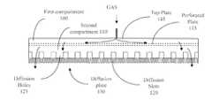
- FIG. 1Aillustrates a plasma processing chamber that may incorporate a showerhead according to the invention.
- FIG. 1Bis a schematic illustrating in a cross section showing major elements of a showerhead according to an embodiment of the invention.
- FIG. 2illustrates a top elevation of the perforated/gas restriction plate, according to an embodiment of the invention, while Detail D illustrates a close-up section of the perforated/gas restriction plate.
- FIG. 3illustrates a cross-section of a section of the showerhead according to an embodiment of the invention.
- FIG. 4illustrates a top view of the diffusion plate according to an embodiment of the invention.
- FIG. 5illustrates a bottom view of the diffusion plate according to an embodiment of the invention.
- FIG. 6illustrates an embodiment in which the diffusion plate is made of a single plate of metal.
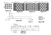
- FIGS. 7A-7Dillustrate different arrangements for the holes and slots.
- FIGS. 8A and 8Billustrate a method according to embodiments of the invention for cost-effectively cutting the diffusion slots.
- FIG. 9illustrate holes design of prior art showerhead.
- FIG. 1Aillustrates a plasma processing chamber 150 that may incorporate a showerhead 155 according to the invention.
- the chamber 150includes a loading gate 160 for loading and unloading substrates.
- a substrate holder 165may be a simple holder, a holder incorporating a heater, a chuck, such as, e.g., an electrostatic chuck, etc.
- the substrate holder 165may hold a single substrate or a plurality of substrates.
- the holdersupports a plurality of substrates 170 , each of which may be lifted from the holder 165 using lift pins 175 .
- the showerhead 155may be coupled to the ground or RF potential of an RF generator, e.g., via an impedance match circuit (not shown).
- FIG. 1Bis a schematic illustrating in a cross section showing major elements of a showerhead according to an embodiment of the invention.
- the showerheadis rectangular, but other shape can be used, depending on the shape of the plasma chamber. Since flat panel displays and solar cells are fabricated inside a rectangular chamber, in this embodiment the showerhead is rectangular.
- the showerheadcomprises perforated plate 115 , which may act as a baffle plate restricting gas flow, and is positioned so as to divide the internal space of the showerhead into a first compartment 100 and a second compartment 110 . Due to the flow restriction action of the baffle plate, first compartment 100 has higher gas pressure than the second compartment.
- the bottom of the showerheadis formed by a diffusion plate 130 , which has elongated diffusion slots 120 at the lower surface, so as to face the substrate being processed.
- the diffusion slotsmay be made large enough to support gas ionization within the slots.
- Diffusion holes 125connect to the diffusion slots 120 , to enable gas from the second compartment 110 to be delivered to the process region via the diffusion slots. Notably, each diffusion hole 125 connects to a plurality of diffusion slots 120 . This feature enables high conductance of the gases into the plasma chamber.
- the gas from a gas sourceenters the showerhead from the top plate 145 and then enters the first compartment 100 .
- the perforated plate 115forces the gas to distribute into the second compartment 110 according to pressure distribution determined by the design of the perforated plate. In this manner, the flow from the first compartment to the second compartment can be controlled.
- the size, number and distribution of the perforationscan be designed to cause the gas to distribute evenly or in a pressure gradient into the second compartment, as desired by the particular design.
- the perforationcan be made to have a diameter in the range of 0.006′′ to 0.500′′.
- the diffusion holes 125then distribute the gas into the diffusion slots 120 .
- the diffusion holes 125are circular and extend vertically to form a fluid passage from the second compartment 110 to the diffusion slots 120 .
- Each diffusion hole 125forms passage to several diffusion slots 120 .
- the diffusion slots 120have rectangular cross-section and each extend horizontally the entire length of the showerhead to enable high conductance of gas.
- the diffusion holescan be made to have a diameter in the range of 0.025′′ to 2.000′′, while the diffusion slots can be made to have a width of 0.010′′ to 1.000′′, a depth of 0.010′′ to 1.000′′, and a slot pitch of 0.015′′ to 6.000′′.
- FIG. 2illustrates a top elevation of the perforated plate 115 , according to an embodiment of the invention, while Detail D illustrates a close-up section of the perforated plate 115 .
- the perforated plate 115has many small holes to serve as a baffle plate, so that gas is delivered controllably from the first compartment 100 to the second compartment 110 . This feature ensures the controlled uniform or gradient distribution of the gas in spite of the high conductance of the diffusion plate. For example, in some applications a uniform gas distribution may be needed, while in other applications center high or center low gas flow may be needed.
- FIG. 3illustrates a partial cross-section of showerhead according to an embodiment of the invention.
- FIG. 3shows the upper gas compartment 100 , the baffle (or flow restriction) plate 115 , lower gas compartment 110 , the gas distribution holes 125 , and the gas distribution slots 120 .
- each gas hole 125connects to several gas slots 120 .
- the holesare staggered such that each row of holes is offset from the rows that are immediately next on each side of it.
- the holesare circular and are vertical, such that each hole forms a passage from the second compartment 110 to several diffusion slots 120 .
- the diffusion slots 120are horizontal and each diffusion slot intersects all diffusion holes 125 in one row. Also, as will be shown in other embodiments, each slot 120 may intersect holes belonging to more than one row.
- FIG. 4illustrates a top view of the diffusion plate 130 , i.e., the view from inside the second compartment 110 , looking down towards the plasma processing chamber.
- FIG. 4shows the round gas holes 125 arranged in rows, wherein each hole 125 leads to several diffusion slots 120 (the slots are shown in broken lines).
- FIG. 4also shows how each successive row of diffusion holes is offset from its immediate neighbor rows, such that the holes are shifted.
- FIG. 5illustrates a bottom view of the diffusion plate 130 , i.e., looking from inside the plasma processing chamber towards the second compartment 110 .
- FIG. 5shows the slots 120 in solid lines and round gas holes 125 in broken lines, behind gas slots 120 .
- Each of the holesis leading to several diffusion slots and each diffusion slot intersect all of the holes in one row of holes.
- the diffusion plateis made of a single plate of metal.
- the bottom surface of the plateis machined to have diffusion slots 620
- the top surface of the plateis drilled to have the rows of holes 625 , such that each drilled hole intersects several diffusion slots.
- each holeintersect three diffusion slots, one of which passes in the center of the hole, while the other two pass at the opposing edge of the hole, as shown in FIG. 6 . Since the rows of holes are staggered, each hole has one diffusion slot passing at its center and two passing at its opposing edges.
- FIG. 7Aillustrate an arrangement wherein multiple rows of holes are provided, wherein each hole in each row intersect three slots and wherein each slot intersect all of the holes in a row.
- the row of holesare aligned, i.e., not staggered. That is, all of the holes 700 a of one row, are aligned with the holes 700 b of the neighboring row of holes.
- the rowsare defined as the collection of holes that are aligned in the slots direction.
- FIG. 7Billustrates the staggered rows arrangement, as shown in FIGS. 3-5 .
- FIG. 7Cillustrates a case wherein the row of holes are aligned (i.e., not staggered) but are shifted in a direction perpendicular to the slots, such that certain slots intersect holes from two neighboring rows of holes. That is, holes 700 f of one row are exactly aligned with holes 700 e of its neighboring row, but they are shifted in a direction perpendicular to the slots, such that holes from one row overlaps slots that are connected to holes from another row.
- FIG. 7Cillustrates a case wherein the row of holes are aligned (i.e., not staggered) but are shifted in a direction perpendicular to the slots, such that certain slots intersect holes from two neighboring rows of holes. That is, holes 700 f of one row are exactly aligned with holes 700 e of its neighboring row, but they are shifted in a direction perpendicular to the slots, such that holes from one row overlaps slots that are connected to holes from another row.
- FIG. 7Dillustrates the case wherein the holes in a neighboring row are staggered and shifted. That is, holes 700 h from one row are positioned midway between holes 700 g of its neighboring row, and the holes 700 h overlap over slots that are also connected to holes 700 g from the neighboring row.
- FIG. 8Aillustrates a cross section along line A-A in FIG. 6 , to enable understanding of a fabrication method according to an embodiment of the invention.
- a circular saw 800also referred to as gang cutter, is used to machine the gas distribution slots 120 in the lower surface of the gas distribution plate 130 .
- a gang cutter having multiple bladescan be used to cut several slots 120 at a single pass.
- Drill 805is used to drill the gas distribution holes 125 from the upper surface of the gas distribution plate.
Landscapes
- Chemical & Material Sciences (AREA)
- Engineering & Computer Science (AREA)
- Physics & Mathematics (AREA)
- Plasma & Fusion (AREA)
- Materials Engineering (AREA)
- Chemical Kinetics & Catalysis (AREA)
- General Chemical & Material Sciences (AREA)
- Mechanical Engineering (AREA)
- Metallurgy (AREA)
- Organic Chemistry (AREA)
- Analytical Chemistry (AREA)
- Drying Of Semiconductors (AREA)
- Chemical Vapour Deposition (AREA)
Abstract
Description
- This application claims priority benefit from U.S. Provisional Patent Application No. 61/252,117, filed Oct. 15, 2009, the disclosure of which is incorporated herein by reference in its entirety.
- 1. Field of the Application
- The invention relates to showerheads for plasma processing chambers, such as for Chemical Vapor Deposition (CVD), Plasma Enhanced Chemical Vapor Deposition (PECVD), and etching of films.
- 2. Related Art
- Apparatus of plasma processing, such as, e.g., plasma enhanced chemical vapor deposition of films, utilize showerhead to introduce the gases into the chamber. Various showerheads for plasma chambers are known in the art. The showerhead delivers processing gas into the plasma processing chamber. Some of the issues considered in designing a showerhead include proper mixing of the gas, control over the distribution of the gas throughout the chamber, control over the temperature of the showerhead and gases within the showerhead, pitting of the showerhead by plasma species, rate of gas delivery, complexity and cost of production, and more.
- The design of the showerhead assembly is critical, as it directly affects the quality of the process in the plasma chamber. For example, the design of the showerhead directly affects the uniformity of the film deposited in PECVD chambers. Uniformity of deposited film becomes more difficult to control as the size of the substrate increases, for example when processing large substrates for LCD or thin-film solar panels. Uniformity is also more difficult to control when performing batch processing, i.e., when forming film on several substrates concurrently in the same chamber. However, as is evident these days, the sizes for LCD becomes larger and larger, and recent popularity of solar panels increases the demands on systems for forming high quality films on large substrates or on multiple substrates concurrently.
- One problem with the current state of the art showerhead is its complexity and cost of manufacturing, mainly due to the side and shape of the gas diffusion holes.
FIG. 9 illustrates a partial view of a showerhead according to the state of the art, in a cross-section view. As seen inFIG. 9 , there are many gas diffusion holes having a complex and expensive shape to manufacture.First holes 900 of small diameter d are drilled from the top surface, generally using a small diameter dill bit that has very limited length, and must be replaced multiple times during the manufacture of a single part. Thenholes 905 of larger diameter are drilled from the bottom surface. In this step it is very important that thebottom holes 905 be coaxially aligned to thetop holes 900, which complicates the fabrication of the showerhead. Also,chamfers holes 900, conventional sand blasting treatment of the showerhead cannot be performed, since it clogs the holes. Therefore, special chemical cleaning must be done instead, followed by close inspection under magnification of all holes to ensure they are all open. - The following summary of the invention is included in order to provide a basic understanding of some aspects and features of the invention. This summary is not an extensive overview of the invention and as such it is not intended to particularly identify key or critical elements of the invention or to delineate the scope of the invention. Its sole purpose is to present some concepts of the invention in a simplified form as a prelude to the more detailed description that is presented below.
- Embodiments of the invention provide a showerhead assembly that is easier and significantly less expensive to manufacture, while having improved gas distribution. Showerheads made according to embodiments of the invention do not require the drilling of large number of small diameter holes. Embodiments of the invention also do not require complex hole shapes. Instead, control over gas distribution gradient or uniformity is done using a baffle plate. A second plate diffuses the gas into the chamber using relatively large diameter holes leading to diffusion slots. Since the diffusion slots are rather large, ionization may take place in the diffusion slots without harming the showerhead. IN such circumstances, the diffusion plate may be referred to as gas ionization plate. According to further embodiments, the showerhead assembly is coupled to the RF generator to also act as an electrode for the plasma chamber.
- A showerhead for a plasma process apparatus for processing substrates, comprising a top plate having gas inlet; a perforated plate positioned below the top plate and distanced from the top plate so as to define an upper gas compartment with the top plate; a diffusion plate positioned below the perforated plate and distanced from the perforated plate so as to define a lower gas compartment, the diffusion plate facing the substrate to be processed; and, wherein the diffusion plate comprises a plurality of elongated diffusion slots on its lower surface and a plurality of diffusion holes on its upper surface, each of the diffusion holes making fluid connection from the lower gas compartment to more than one of the diffusion slots.
- A showerhead for a plasma process apparatus for processing substrates, comprising a showerhead body comprising a top plate and a bottom plate defining a cavity in between; a gas inlet formed in the top plate; a perforated plate positioned between the top plate and the bottom plate and dissecting the cavity into an upper gas compartment and a lower gas compartment; and, wherein the bottom plate comprises a plurality of elongated diffusion slots on its lower surface and a plurality of diffusion holes on its upper surface, each of the diffusion holes making fluid connection from the lower gas compartment to more than one of the diffusion slots.
- According to embodiments of the invention, a simple and cost-effective method for fabricating a gas ionization plate is disclosed, the method comprising fabricating a plate; using gang cutter to form a plurality of gas ionization slots on the lower surface of the plate; and, drilling a plurality of gas distribution holes from the top surface of the plate such that each holes reaches and opened to a plurality of the gas ionization slots.
- Other aspects and features of the invention would be apparent from the detailed description, which is made with reference to the following drawings. It should be appreciated that the detailed description and the drawings provides various non-limiting examples of various embodiments of the invention, which is defined by the appended claims.
- The accompanying drawings, which are incorporated in and constitute a part of this specification, exemplify the embodiments of the present invention and, together with the description, serve to explain and illustrate principles of the invention. The drawings are intended to illustrate features of the exemplary embodiments in a diagrammatic manner. The drawings are not intended to depict every feature of actual embodiments nor relative dimensions of the depicted elements, and are not drawn to scale.
FIG. 1A illustrates a plasma processing chamber that may incorporate a showerhead according to the invention.FIG. 1B is a schematic illustrating in a cross section showing major elements of a showerhead according to an embodiment of the invention.FIG. 2 illustrates a top elevation of the perforated/gas restriction plate, according to an embodiment of the invention, while Detail D illustrates a close-up section of the perforated/gas restriction plate.FIG. 3 illustrates a cross-section of a section of the showerhead according to an embodiment of the invention.FIG. 4 illustrates a top view of the diffusion plate according to an embodiment of the invention.FIG. 5 illustrates a bottom view of the diffusion plate according to an embodiment of the invention.FIG. 6 illustrates an embodiment in which the diffusion plate is made of a single plate of metal.FIGS. 7A-7D illustrate different arrangements for the holes and slots.FIGS. 8A and 8B illustrate a method according to embodiments of the invention for cost-effectively cutting the diffusion slots.FIG. 9 illustrate holes design of prior art showerhead.FIG. 1A illustrates aplasma processing chamber 150 that may incorporate ashowerhead 155 according to the invention. In this example thechamber 150 includes aloading gate 160 for loading and unloading substrates. Asubstrate holder 165 may be a simple holder, a holder incorporating a heater, a chuck, such as, e.g., an electrostatic chuck, etc. Thesubstrate holder 165 may hold a single substrate or a plurality of substrates. In this example, the holder supports a plurality ofsubstrates 170, each of which may be lifted from theholder 165 using lift pins175. Also, theshowerhead 155 may be coupled to the ground or RF potential of an RF generator, e.g., via an impedance match circuit (not shown).FIG. 1B is a schematic illustrating in a cross section showing major elements of a showerhead according to an embodiment of the invention. In this particular example the showerhead is rectangular, but other shape can be used, depending on the shape of the plasma chamber. Since flat panel displays and solar cells are fabricated inside a rectangular chamber, in this embodiment the showerhead is rectangular.- The showerhead comprises perforated
plate 115, which may act as a baffle plate restricting gas flow, and is positioned so as to divide the internal space of the showerhead into afirst compartment 100 and asecond compartment 110. Due to the flow restriction action of the baffle plate,first compartment 100 has higher gas pressure than the second compartment. The bottom of the showerhead is formed by adiffusion plate 130, which has elongateddiffusion slots 120 at the lower surface, so as to face the substrate being processed. The diffusion slots may be made large enough to support gas ionization within the slots. Diffusion holes125 connect to thediffusion slots 120, to enable gas from thesecond compartment 110 to be delivered to the process region via the diffusion slots. Notably, eachdiffusion hole 125 connects to a plurality ofdiffusion slots 120. This feature enables high conductance of the gases into the plasma chamber. - As is shown by the arrows in
FIG. 1B , the gas from a gas source enters the showerhead from thetop plate 145 and then enters thefirst compartment 100. Theperforated plate 115 forces the gas to distribute into thesecond compartment 110 according to pressure distribution determined by the design of the perforated plate. In this manner, the flow from the first compartment to the second compartment can be controlled. For example, the size, number and distribution of the perforations can be designed to cause the gas to distribute evenly or in a pressure gradient into the second compartment, as desired by the particular design. According to embodiments of the invention the perforation can be made to have a diameter in the range of 0.006″ to 0.500″. - The diffusion holes125 then distribute the gas into the
diffusion slots 120. In this embodiment the diffusion holes125 are circular and extend vertically to form a fluid passage from thesecond compartment 110 to thediffusion slots 120. Eachdiffusion hole 125 forms passage toseveral diffusion slots 120. In this embodiment thediffusion slots 120 have rectangular cross-section and each extend horizontally the entire length of the showerhead to enable high conductance of gas. According to embodiments of the invention the diffusion holes can be made to have a diameter in the range of 0.025″ to 2.000″, while the diffusion slots can be made to have a width of 0.010″ to 1.000″, a depth of 0.010″ to 1.000″, and a slot pitch of 0.015″ to 6.000″. FIG. 2 illustrates a top elevation of theperforated plate 115, according to an embodiment of the invention, while Detail D illustrates a close-up section of theperforated plate 115. Theperforated plate 115 has many small holes to serve as a baffle plate, so that gas is delivered controllably from thefirst compartment 100 to thesecond compartment 110. This feature ensures the controlled uniform or gradient distribution of the gas in spite of the high conductance of the diffusion plate. For example, in some applications a uniform gas distribution may be needed, while in other applications center high or center low gas flow may be needed.FIG. 3 illustrates a partial cross-section of showerhead according to an embodiment of the invention.FIG. 3 shows theupper gas compartment 100, the baffle (or flow restriction)plate 115,lower gas compartment 110, the gas distribution holes125, and thegas distribution slots 120. As shown, in this embodiment eachgas hole 125 connects toseveral gas slots 120. Also, in this embodiment the holes are staggered such that each row of holes is offset from the rows that are immediately next on each side of it. As explained above, in this embodiment the holes are circular and are vertical, such that each hole forms a passage from thesecond compartment 110 toseveral diffusion slots 120. Of course, other hole shapes can be used. Thediffusion slots 120 are horizontal and each diffusion slot intersects alldiffusion holes 125 in one row. Also, as will be shown in other embodiments, eachslot 120 may intersect holes belonging to more than one row.FIG. 4 illustrates a top view of thediffusion plate 130, i.e., the view from inside thesecond compartment 110, looking down towards the plasma processing chamber.FIG. 4 shows theround gas holes 125 arranged in rows, wherein eachhole 125 leads to several diffusion slots120 (the slots are shown in broken lines).FIG. 4 also shows how each successive row of diffusion holes is offset from its immediate neighbor rows, such that the holes are shifted.FIG. 5 illustrates a bottom view of thediffusion plate 130, i.e., looking from inside the plasma processing chamber towards thesecond compartment 110.FIG. 5 shows theslots 120 in solid lines andround gas holes 125 in broken lines, behindgas slots 120. Each of the holes is leading to several diffusion slots and each diffusion slot intersect all of the holes in one row of holes.- According to the embodiment illustrated in
FIG. 6 , the diffusion plate is made of a single plate of metal. The bottom surface of the plate is machined to havediffusion slots 620, while the top surface of the plate is drilled to have the rows ofholes 625, such that each drilled hole intersects several diffusion slots. In one embodiment, each hole intersect three diffusion slots, one of which passes in the center of the hole, while the other two pass at the opposing edge of the hole, as shown inFIG. 6 . Since the rows of holes are staggered, each hole has one diffusion slot passing at its center and two passing at its opposing edges. - As noted above, other arrangements for the gas distribution holes and gas distribution slots can be used. For example,
FIG. 7A illustrate an arrangement wherein multiple rows of holes are provided, wherein each hole in each row intersect three slots and wherein each slot intersect all of the holes in a row. The row of holes are aligned, i.e., not staggered. That is, all of theholes 700aof one row, are aligned with theholes 700bof the neighboring row of holes. In this respect, the rows are defined as the collection of holes that are aligned in the slots direction.FIG. 7B , on the other hand, illustrates the staggered rows arrangement, as shown inFIGS. 3-5 . That is, holes700dof one row are shifted from theholes 700cof its neighboring row. The shift is such that each holes700dis aligned exactly midway between twoholes 700cof the neighboring row.FIG. 7C illustrates a case wherein the row of holes are aligned (i.e., not staggered) but are shifted in a direction perpendicular to the slots, such that certain slots intersect holes from two neighboring rows of holes. That is, holes700fof one row are exactly aligned withholes 700eof its neighboring row, but they are shifted in a direction perpendicular to the slots, such that holes from one row overlaps slots that are connected to holes from another row.FIG. 7D illustrates the case wherein the holes in a neighboring row are staggered and shifted. That is, holes700hfrom one row are positioned midway betweenholes 700gof its neighboring row, and theholes 700hoverlap over slots that are also connected toholes 700gfrom the neighboring row. FIG. 8A illustrates a cross section along line A-A inFIG. 6 , to enable understanding of a fabrication method according to an embodiment of the invention. As shown inFIG. 8A , acircular saw 800, also referred to as gang cutter, is used to machine thegas distribution slots 120 in the lower surface of thegas distribution plate 130. As shown in FIG.8B, a gang cutter having multiple blades can be used to cutseveral slots 120 at a single pass. Drill805 is used to drill the gas distribution holes125 from the upper surface of the gas distribution plate.- It should be understood that processes and techniques described herein are not inherently related to any particular apparatus and may be implemented by any suitable combination of components. Further, various types of general purpose devices may be used in accordance with the teachings described herein. It may also prove advantageous to construct specialized apparatus to perform the method steps described herein.
- The present invention has been described in relation to particular examples, which are intended in all respects to be illustrative rather than restrictive. Those skilled in the art will appreciate that many different combinations of hardware, software, and firmware will be suitable for practicing the present invention. Moreover, other implementations of the invention will be apparent to those skilled in the art from consideration of the specification and practice of the invention disclosed herein. It is intended that the specification and examples be considered as exemplary only, with a true scope and spirit of the invention being indicated by the following claims.
Claims (22)
Priority Applications (1)
| Application Number | Priority Date | Filing Date | Title |
|---|---|---|---|
| US12/906,053US8617349B2 (en) | 2009-10-15 | 2010-10-15 | Showerhead assembly for plasma processing chamber |
Applications Claiming Priority (2)
| Application Number | Priority Date | Filing Date | Title |
|---|---|---|---|
| US25211709P | 2009-10-15 | 2009-10-15 | |
| US12/906,053US8617349B2 (en) | 2009-10-15 | 2010-10-15 | Showerhead assembly for plasma processing chamber |
Publications (2)
| Publication Number | Publication Date |
|---|---|
| US20110088847A1true US20110088847A1 (en) | 2011-04-21 |
| US8617349B2 US8617349B2 (en) | 2013-12-31 |
Family
ID=43566651
Family Applications (1)
| Application Number | Title | Priority Date | Filing Date |
|---|---|---|---|
| US12/906,053Active2032-03-22US8617349B2 (en) | 2009-10-15 | 2010-10-15 | Showerhead assembly for plasma processing chamber |
Country Status (5)
| Country | Link |
|---|---|
| US (1) | US8617349B2 (en) |
| EP (1) | EP2312613B1 (en) |
| KR (1) | KR101687029B1 (en) |
| CN (1) | CN102051600B (en) |
| TW (1) | TWI430714B (en) |
Cited By (70)
| Publication number | Priority date | Publication date | Assignee | Title |
|---|---|---|---|---|
| US20120115290A1 (en)* | 2010-11-04 | 2012-05-10 | Semiconductor Energy Laboratory Co., Ltd. | Manufacturing method of crystalline semiconductor film and manufacturing method of semiconductor device |
| US8617349B2 (en)* | 2009-10-15 | 2013-12-31 | Orbotech LT Solar, LLC. | Showerhead assembly for plasma processing chamber |
| US20140179114A1 (en)* | 2012-12-21 | 2014-06-26 | Bart J. van Schravendijk | Radical source design for remote plasma atomic layer deposition |
| CN104099583A (en)* | 2013-04-09 | 2014-10-15 | 北京北方微电子基地设备工艺研究中心有限责任公司 | Air inlet unit, reaction chamber and plasma processing apparatus |
| CN104952760A (en)* | 2014-03-24 | 2015-09-30 | 北京北方微电子基地设备工艺研究中心有限责任公司 | Intake device and semiconductor processing equipment |
| US20150303037A1 (en)* | 2012-12-27 | 2015-10-22 | Moohan Co., Ltd. | Substrate Processing Apparatus |
| US10023959B2 (en) | 2015-05-26 | 2018-07-17 | Lam Research Corporation | Anti-transient showerhead |
| US10424464B2 (en) | 2015-08-07 | 2019-09-24 | Applied Materials, Inc. | Oxide etch selectivity systems and methods |
| US10468285B2 (en) | 2015-02-03 | 2019-11-05 | Applied Materials, Inc. | High temperature chuck for plasma processing systems |
| US10468267B2 (en) | 2017-05-31 | 2019-11-05 | Applied Materials, Inc. | Water-free etching methods |
| US10468276B2 (en) | 2015-08-06 | 2019-11-05 | Applied Materials, Inc. | Thermal management systems and methods for wafer processing systems |
| US10490418B2 (en) | 2014-10-14 | 2019-11-26 | Applied Materials, Inc. | Systems and methods for internal surface conditioning assessment in plasma processing equipment |
| US10490406B2 (en) | 2018-04-10 | 2019-11-26 | Appled Materials, Inc. | Systems and methods for material breakthrough |
| US10497573B2 (en) | 2018-03-13 | 2019-12-03 | Applied Materials, Inc. | Selective atomic layer etching of semiconductor materials |
| US10504754B2 (en) | 2016-05-19 | 2019-12-10 | Applied Materials, Inc. | Systems and methods for improved semiconductor etching and component protection |
| US10522371B2 (en) | 2016-05-19 | 2019-12-31 | Applied Materials, Inc. | Systems and methods for improved semiconductor etching and component protection |
| US10529737B2 (en) | 2017-02-08 | 2020-01-07 | Applied Materials, Inc. | Accommodating imperfectly aligned memory holes |
| US10541246B2 (en) | 2017-06-26 | 2020-01-21 | Applied Materials, Inc. | 3D flash memory cells which discourage cross-cell electrical tunneling |
| US10541113B2 (en) | 2016-10-04 | 2020-01-21 | Applied Materials, Inc. | Chamber with flow-through source |
| US10541184B2 (en) | 2017-07-11 | 2020-01-21 | Applied Materials, Inc. | Optical emission spectroscopic techniques for monitoring etching |
| US10546729B2 (en) | 2016-10-04 | 2020-01-28 | Applied Materials, Inc. | Dual-channel showerhead with improved profile |
| US10573496B2 (en) | 2014-12-09 | 2020-02-25 | Applied Materials, Inc. | Direct outlet toroidal plasma source |
| US10573527B2 (en) | 2018-04-06 | 2020-02-25 | Applied Materials, Inc. | Gas-phase selective etching systems and methods |
| US10593523B2 (en) | 2014-10-14 | 2020-03-17 | Applied Materials, Inc. | Systems and methods for internal surface conditioning in plasma processing equipment |
| US10593553B2 (en) | 2017-08-04 | 2020-03-17 | Applied Materials, Inc. | Germanium etching systems and methods |
| US10593560B2 (en) | 2018-03-01 | 2020-03-17 | Applied Materials, Inc. | Magnetic induction plasma source for semiconductor processes and equipment |
| US10600639B2 (en) | 2016-11-14 | 2020-03-24 | Applied Materials, Inc. | SiN spacer profile patterning |
| US10607867B2 (en) | 2015-08-06 | 2020-03-31 | Applied Materials, Inc. | Bolted wafer chuck thermal management systems and methods for wafer processing systems |
| US10604841B2 (en) | 2016-12-14 | 2020-03-31 | Lam Research Corporation | Integrated showerhead with thermal control for delivering radical and precursor gas to a downstream chamber to enable remote plasma film deposition |
| US10615047B2 (en) | 2018-02-28 | 2020-04-07 | Applied Materials, Inc. | Systems and methods to form airgaps |
| US10629473B2 (en) | 2016-09-09 | 2020-04-21 | Applied Materials, Inc. | Footing removal for nitride spacer |
| US10672642B2 (en) | 2018-07-24 | 2020-06-02 | Applied Materials, Inc. | Systems and methods for pedestal configuration |
| US10679870B2 (en) | 2018-02-15 | 2020-06-09 | Applied Materials, Inc. | Semiconductor processing chamber multistage mixing apparatus |
| US10699879B2 (en) | 2018-04-17 | 2020-06-30 | Applied Materials, Inc. | Two piece electrode assembly with gap for plasma control |
| US10727080B2 (en) | 2017-07-07 | 2020-07-28 | Applied Materials, Inc. | Tantalum-containing material removal |
| US10755941B2 (en) | 2018-07-06 | 2020-08-25 | Applied Materials, Inc. | Self-limiting selective etching systems and methods |
| US10770346B2 (en) | 2016-11-11 | 2020-09-08 | Applied Materials, Inc. | Selective cobalt removal for bottom up gapfill |
| US10854426B2 (en) | 2018-01-08 | 2020-12-01 | Applied Materials, Inc. | Metal recess for semiconductor structures |
| US10872778B2 (en) | 2018-07-06 | 2020-12-22 | Applied Materials, Inc. | Systems and methods utilizing solid-phase etchants |
| US10886137B2 (en) | 2018-04-30 | 2021-01-05 | Applied Materials, Inc. | Selective nitride removal |
| US10892198B2 (en) | 2018-09-14 | 2021-01-12 | Applied Materials, Inc. | Systems and methods for improved performance in semiconductor processing |
| US10903054B2 (en) | 2017-12-19 | 2021-01-26 | Applied Materials, Inc. | Multi-zone gas distribution systems and methods |
| US10903052B2 (en) | 2017-02-03 | 2021-01-26 | Applied Materials, Inc. | Systems and methods for radial and azimuthal control of plasma uniformity |
| US10920319B2 (en) | 2019-01-11 | 2021-02-16 | Applied Materials, Inc. | Ceramic showerheads with conductive electrodes |
| US10920320B2 (en) | 2017-06-16 | 2021-02-16 | Applied Materials, Inc. | Plasma health determination in semiconductor substrate processing reactors |
| US10943834B2 (en) | 2017-03-13 | 2021-03-09 | Applied Materials, Inc. | Replacement contact process |
| WO2021050386A1 (en)* | 2019-09-13 | 2021-03-18 | Applied Materials, Inc. | Semiconductor processing chamber |
| US10964512B2 (en) | 2018-02-15 | 2021-03-30 | Applied Materials, Inc. | Semiconductor processing chamber multistage mixing apparatus and methods |
| US11004689B2 (en) | 2018-03-12 | 2021-05-11 | Applied Materials, Inc. | Thermal silicon etch |
| US11017986B2 (en) | 2017-06-06 | 2021-05-25 | Applied Materials, Inc. | Deposition radial and edge profile tunability through independent control of TEOS flow |
| US11015247B2 (en) | 2017-12-08 | 2021-05-25 | Lam Research Corporation | Integrated showerhead with improved hole pattern for delivering radical and precursor gas to a downstream chamber to enable remote plasma film deposition |
| US11024486B2 (en) | 2013-02-08 | 2021-06-01 | Applied Materials, Inc. | Semiconductor processing systems having multiple plasma configurations |
| US11049755B2 (en) | 2018-09-14 | 2021-06-29 | Applied Materials, Inc. | Semiconductor substrate supports with embedded RF shield |
| US11062887B2 (en) | 2018-09-17 | 2021-07-13 | Applied Materials, Inc. | High temperature RF heater pedestals |
| US11072859B2 (en)* | 2016-03-29 | 2021-07-27 | Kokusai Electric Corporation | Substrate processing apparatus, method of manufacturing semiconductor device, and recording medium |
| US11101136B2 (en) | 2017-08-07 | 2021-08-24 | Applied Materials, Inc. | Process window widening using coated parts in plasma etch processes |
| US11121002B2 (en) | 2018-10-24 | 2021-09-14 | Applied Materials, Inc. | Systems and methods for etching metals and metal derivatives |
| US11239061B2 (en) | 2014-11-26 | 2022-02-01 | Applied Materials, Inc. | Methods and systems to enhance process uniformity |
| US11264213B2 (en) | 2012-09-21 | 2022-03-01 | Applied Materials, Inc. | Chemical control features in wafer process equipment |
| US11276559B2 (en) | 2017-05-17 | 2022-03-15 | Applied Materials, Inc. | Semiconductor processing chamber for multiple precursor flow |
| US11276590B2 (en) | 2017-05-17 | 2022-03-15 | Applied Materials, Inc. | Multi-zone semiconductor substrate supports |
| US11328909B2 (en) | 2017-12-22 | 2022-05-10 | Applied Materials, Inc. | Chamber conditioning and removal processes |
| US11417534B2 (en) | 2018-09-21 | 2022-08-16 | Applied Materials, Inc. | Selective material removal |
| US11437242B2 (en) | 2018-11-27 | 2022-09-06 | Applied Materials, Inc. | Selective removal of silicon-containing materials |
| US11476093B2 (en) | 2015-08-27 | 2022-10-18 | Applied Materials, Inc. | Plasma etching systems and methods with secondary plasma injection |
| US11594428B2 (en) | 2015-02-03 | 2023-02-28 | Applied Materials, Inc. | Low temperature chuck for plasma processing systems |
| US11682560B2 (en) | 2018-10-11 | 2023-06-20 | Applied Materials, Inc. | Systems and methods for hafnium-containing film removal |
| US11721527B2 (en) | 2019-01-07 | 2023-08-08 | Applied Materials, Inc. | Processing chamber mixing systems |
| US12057329B2 (en) | 2016-06-29 | 2024-08-06 | Applied Materials, Inc. | Selective etch using material modification and RF pulsing |
| US12340979B2 (en) | 2017-05-17 | 2025-06-24 | Applied Materials, Inc. | Semiconductor processing chamber for improved precursor flow |
Families Citing this family (12)
| Publication number | Priority date | Publication date | Assignee | Title |
|---|---|---|---|---|
| KR101464228B1 (en)* | 2007-01-12 | 2014-11-21 | 비코 인스트루먼츠 인코포레이티드 | Gas treatment systems |
| JP5777615B2 (en)* | 2009-07-15 | 2015-09-09 | アプライド マテリアルズ インコーポレイテッドApplied Materials,Incorporated | Flow control mechanism of CVD chamber |
| JP5835722B2 (en) | 2009-12-10 | 2015-12-24 | オルボテック エルティ ソラー,エルエルシー | Automatic ranking multi-directional serial processor |
| US8459276B2 (en) | 2011-05-24 | 2013-06-11 | Orbotech LT Solar, LLC. | Broken wafer recovery system |
| US20130108792A1 (en)* | 2011-10-26 | 2013-05-02 | Pinecone Material Inc. | Loading and unloading system for thin film formation and method thereof |
| CN102978589B (en)* | 2012-12-04 | 2014-10-15 | 中国科学院电工研究所 | PECVD (plasma enhanced chemical vapor deposition) spray electrode |
| US9865437B2 (en) | 2014-12-30 | 2018-01-09 | Applied Materials, Inc. | High conductance process kit |
| CN104835876B (en)* | 2015-04-27 | 2018-01-05 | 北京金晟阳光科技有限公司 | The uniform distribution device of gas |
| US20180230597A1 (en)* | 2017-02-14 | 2018-08-16 | Applied Materials, Inc. | Method and apparatus of remote plasmas flowable cvd chamber |
| CN110391120B (en)* | 2018-04-17 | 2022-02-22 | 北京北方华创微电子装备有限公司 | Shower nozzle and plasma processing cavity |
| KR102204026B1 (en)* | 2018-07-06 | 2021-01-18 | 주식회사 케이에스엠컴포넌트 | Ceramic showerhead and chemical vapor deposition device with the same |
| CN112192154A (en)* | 2020-09-30 | 2021-01-08 | 靖江先锋半导体科技有限公司 | Processing technology of gas spraying disc for etching machine |
Citations (16)
| Publication number | Priority date | Publication date | Assignee | Title |
|---|---|---|---|---|
| US4612077A (en)* | 1985-07-29 | 1986-09-16 | The Perkin-Elmer Corporation | Electrode for plasma etching system |
| US5136975A (en)* | 1990-06-21 | 1992-08-11 | Watkins-Johnson Company | Injector and method for delivering gaseous chemicals to a surface |
| US5746875A (en)* | 1994-09-16 | 1998-05-05 | Applied Materials, Inc. | Gas injection slit nozzle for a plasma process reactor |
| US6036782A (en)* | 1997-10-07 | 2000-03-14 | Tokyo Electron Limited | Shower head |
| US6113984A (en)* | 1996-08-07 | 2000-09-05 | Concept Systems Design, Inc. | Gas injection system for CVD reactors |
| US6586886B1 (en)* | 2001-12-19 | 2003-07-01 | Applied Materials, Inc. | Gas distribution plate electrode for a plasma reactor |
| US20030140851A1 (en)* | 2002-01-25 | 2003-07-31 | Applied Materials, Inc. | Gas distribution showerhead |
| US20040060514A1 (en)* | 2002-01-25 | 2004-04-01 | Applied Materials, Inc. A Delaware Corporation | Gas distribution showerhead |
| US20050183827A1 (en)* | 2004-02-24 | 2005-08-25 | Applied Materials, Inc. | Showerhead mounting to accommodate thermal expansion |
| US20070181531A1 (en)* | 2006-02-06 | 2007-08-09 | Tokyo Electron Limited | Plasma processing apparatus and plasma processing method |
| US7270713B2 (en)* | 2003-01-07 | 2007-09-18 | Applied Materials, Inc. | Tunable gas distribution plate assembly |
| US20080090417A1 (en)* | 2006-10-16 | 2008-04-17 | Lam Research Corporation | Upper electrode backing member with particle reducing features |
| US20080196666A1 (en)* | 2007-02-20 | 2008-08-21 | Masato Toshima | Shower head and cvd apparatus using the same |
| US20110011338A1 (en)* | 2009-07-15 | 2011-01-20 | Applied Materials, Inc. | Flow control features of cvd chambers |
| US8152923B2 (en)* | 2007-01-12 | 2012-04-10 | Veeco Instruments Inc. | Gas treatment systems |
| US8454850B2 (en)* | 2009-09-02 | 2013-06-04 | Air Products And Chemicals, Inc. | Method for the removal of surface oxides by electron attachment |
Family Cites Families (15)
| Publication number | Priority date | Publication date | Assignee | Title |
|---|---|---|---|---|
| US4590042A (en)* | 1984-12-24 | 1986-05-20 | Tegal Corporation | Plasma reactor having slotted manifold |
| KR950020993A (en)* | 1993-12-22 | 1995-07-26 | 김광호 | Semiconductor manufacturing device |
| US5551327A (en)* | 1994-08-22 | 1996-09-03 | Hamby; William D. | Adjusting means for multi-blade cutting apparatus |
| JP2000290777A (en)* | 1999-04-07 | 2000-10-17 | Tokyo Electron Ltd | Gas treating device, buffle member, and gas treating method |
| JP3965258B2 (en)* | 1999-04-30 | 2007-08-29 | 日本碍子株式会社 | Ceramic gas supply structure for semiconductor manufacturing equipment |
| US6502530B1 (en)* | 2000-04-26 | 2003-01-07 | Unaxis Balzers Aktiengesellschaft | Design of gas injection for the electrode in a capacitively coupled RF plasma reactor |
| KR100516844B1 (en)* | 2001-01-22 | 2005-09-26 | 동경 엘렉트론 주식회사 | Device and method for treatment |
| TWI224815B (en) | 2001-08-01 | 2004-12-01 | Tokyo Electron Ltd | Gas processing apparatus and gas processing method |
| US8328939B2 (en)* | 2004-05-12 | 2012-12-11 | Applied Materials, Inc. | Diffuser plate with slit valve compensation |
| KR100747735B1 (en) | 2005-05-13 | 2007-08-09 | 주식회사 테스 | Semiconductor manufacturing equipment |
| US7976631B2 (en)* | 2007-10-16 | 2011-07-12 | Applied Materials, Inc. | Multi-gas straight channel showerhead |
| US20090095221A1 (en)* | 2007-10-16 | 2009-04-16 | Alexander Tam | Multi-gas concentric injection showerhead |
| US20090095222A1 (en)* | 2007-10-16 | 2009-04-16 | Alexander Tam | Multi-gas spiral channel showerhead |
| US8876024B2 (en) | 2008-01-10 | 2014-11-04 | Applied Materials, Inc. | Heated showerhead assembly |
| TWI430714B (en)* | 2009-10-15 | 2014-03-11 | Orbotech Lt Solar Llc | Showerhead assembly for plasma processing chamber and method for fabricating gas ionization plate thereof |
- 2010
- 2010-10-14TWTW099135138Apatent/TWI430714B/enactive
- 2010-10-15USUS12/906,053patent/US8617349B2/enactiveActive
- 2010-10-15KRKR1020100100808Apatent/KR101687029B1/enactiveActive
- 2010-10-15EPEP10013687.8Apatent/EP2312613B1/enactiveActive
- 2010-10-15CNCN201010552244.2Apatent/CN102051600B/enactiveActive
Patent Citations (20)
| Publication number | Priority date | Publication date | Assignee | Title |
|---|---|---|---|---|
| US4612077A (en)* | 1985-07-29 | 1986-09-16 | The Perkin-Elmer Corporation | Electrode for plasma etching system |
| US5136975A (en)* | 1990-06-21 | 1992-08-11 | Watkins-Johnson Company | Injector and method for delivering gaseous chemicals to a surface |
| US5746875A (en)* | 1994-09-16 | 1998-05-05 | Applied Materials, Inc. | Gas injection slit nozzle for a plasma process reactor |
| US6113984A (en)* | 1996-08-07 | 2000-09-05 | Concept Systems Design, Inc. | Gas injection system for CVD reactors |
| US6036782A (en)* | 1997-10-07 | 2000-03-14 | Tokyo Electron Limited | Shower head |
| US6586886B1 (en)* | 2001-12-19 | 2003-07-01 | Applied Materials, Inc. | Gas distribution plate electrode for a plasma reactor |
| US6677712B2 (en)* | 2001-12-19 | 2004-01-13 | Applied Materials Inc. | Gas distribution plate electrode for a plasma receptor |
| US20030140851A1 (en)* | 2002-01-25 | 2003-07-31 | Applied Materials, Inc. | Gas distribution showerhead |
| US20040060514A1 (en)* | 2002-01-25 | 2004-04-01 | Applied Materials, Inc. A Delaware Corporation | Gas distribution showerhead |
| US6793733B2 (en)* | 2002-01-25 | 2004-09-21 | Applied Materials Inc. | Gas distribution showerhead |
| US7270713B2 (en)* | 2003-01-07 | 2007-09-18 | Applied Materials, Inc. | Tunable gas distribution plate assembly |
| US20050183827A1 (en)* | 2004-02-24 | 2005-08-25 | Applied Materials, Inc. | Showerhead mounting to accommodate thermal expansion |
| US20070181531A1 (en)* | 2006-02-06 | 2007-08-09 | Tokyo Electron Limited | Plasma processing apparatus and plasma processing method |
| US20080090417A1 (en)* | 2006-10-16 | 2008-04-17 | Lam Research Corporation | Upper electrode backing member with particle reducing features |
| US7854820B2 (en)* | 2006-10-16 | 2010-12-21 | Lam Research Corporation | Upper electrode backing member with particle reducing features |
| US8152923B2 (en)* | 2007-01-12 | 2012-04-10 | Veeco Instruments Inc. | Gas treatment systems |
| US8287646B2 (en)* | 2007-01-12 | 2012-10-16 | Veeco Instruments Inc. | Gas treatment systems |
| US20080196666A1 (en)* | 2007-02-20 | 2008-08-21 | Masato Toshima | Shower head and cvd apparatus using the same |
| US20110011338A1 (en)* | 2009-07-15 | 2011-01-20 | Applied Materials, Inc. | Flow control features of cvd chambers |
| US8454850B2 (en)* | 2009-09-02 | 2013-06-04 | Air Products And Chemicals, Inc. | Method for the removal of surface oxides by electron attachment |
Cited By (98)
| Publication number | Priority date | Publication date | Assignee | Title |
|---|---|---|---|---|
| US8617349B2 (en)* | 2009-10-15 | 2013-12-31 | Orbotech LT Solar, LLC. | Showerhead assembly for plasma processing chamber |
| US8895116B2 (en)* | 2010-11-04 | 2014-11-25 | Semiconductor Energy Laboratory Co., Ltd. | Manufacturing method of crystalline semiconductor film and manufacturing method of semiconductor device |
| US20120115290A1 (en)* | 2010-11-04 | 2012-05-10 | Semiconductor Energy Laboratory Co., Ltd. | Manufacturing method of crystalline semiconductor film and manufacturing method of semiconductor device |
| US11264213B2 (en) | 2012-09-21 | 2022-03-01 | Applied Materials, Inc. | Chemical control features in wafer process equipment |
| US10316409B2 (en)* | 2012-12-21 | 2019-06-11 | Novellus Systems, Inc. | Radical source design for remote plasma atomic layer deposition |
| KR20140081755A (en)* | 2012-12-21 | 2014-07-01 | 노벨러스 시스템즈, 인코포레이티드 | Radical source design for remote plasma atomic layer deposition |
| US11053587B2 (en)* | 2012-12-21 | 2021-07-06 | Novellus Systems, Inc. | Radical source design for remote plasma atomic layer deposition |
| KR102174446B1 (en) | 2012-12-21 | 2020-11-05 | 노벨러스 시스템즈, 인코포레이티드 | Radical source design for remote plasma atomic layer deposition |
| US20140179114A1 (en)* | 2012-12-21 | 2014-06-26 | Bart J. van Schravendijk | Radical source design for remote plasma atomic layer deposition |
| US20150303037A1 (en)* | 2012-12-27 | 2015-10-22 | Moohan Co., Ltd. | Substrate Processing Apparatus |
| US11075060B2 (en)* | 2012-12-27 | 2021-07-27 | Jusung Engineering Co., Ltd. | Substrate processing apparatus |
| US11024486B2 (en) | 2013-02-08 | 2021-06-01 | Applied Materials, Inc. | Semiconductor processing systems having multiple plasma configurations |
| CN104099583A (en)* | 2013-04-09 | 2014-10-15 | 北京北方微电子基地设备工艺研究中心有限责任公司 | Air inlet unit, reaction chamber and plasma processing apparatus |
| CN104952760A (en)* | 2014-03-24 | 2015-09-30 | 北京北方微电子基地设备工艺研究中心有限责任公司 | Intake device and semiconductor processing equipment |
| US10796922B2 (en) | 2014-10-14 | 2020-10-06 | Applied Materials, Inc. | Systems and methods for internal surface conditioning assessment in plasma processing equipment |
| US10490418B2 (en) | 2014-10-14 | 2019-11-26 | Applied Materials, Inc. | Systems and methods for internal surface conditioning assessment in plasma processing equipment |
| US10707061B2 (en) | 2014-10-14 | 2020-07-07 | Applied Materials, Inc. | Systems and methods for internal surface conditioning in plasma processing equipment |
| US10593523B2 (en) | 2014-10-14 | 2020-03-17 | Applied Materials, Inc. | Systems and methods for internal surface conditioning in plasma processing equipment |
| US11239061B2 (en) | 2014-11-26 | 2022-02-01 | Applied Materials, Inc. | Methods and systems to enhance process uniformity |
| US11637002B2 (en) | 2014-11-26 | 2023-04-25 | Applied Materials, Inc. | Methods and systems to enhance process uniformity |
| US10573496B2 (en) | 2014-12-09 | 2020-02-25 | Applied Materials, Inc. | Direct outlet toroidal plasma source |
| US10468285B2 (en) | 2015-02-03 | 2019-11-05 | Applied Materials, Inc. | High temperature chuck for plasma processing systems |
| US11594428B2 (en) | 2015-02-03 | 2023-02-28 | Applied Materials, Inc. | Low temperature chuck for plasma processing systems |
| US12009228B2 (en) | 2015-02-03 | 2024-06-11 | Applied Materials, Inc. | Low temperature chuck for plasma processing systems |
| US10494717B2 (en) | 2015-05-26 | 2019-12-03 | Lam Research Corporation | Anti-transient showerhead |
| US10023959B2 (en) | 2015-05-26 | 2018-07-17 | Lam Research Corporation | Anti-transient showerhead |
| US10468276B2 (en) | 2015-08-06 | 2019-11-05 | Applied Materials, Inc. | Thermal management systems and methods for wafer processing systems |
| US10607867B2 (en) | 2015-08-06 | 2020-03-31 | Applied Materials, Inc. | Bolted wafer chuck thermal management systems and methods for wafer processing systems |
| US11158527B2 (en) | 2015-08-06 | 2021-10-26 | Applied Materials, Inc. | Thermal management systems and methods for wafer processing systems |
| US10424463B2 (en) | 2015-08-07 | 2019-09-24 | Applied Materials, Inc. | Oxide etch selectivity systems and methods |
| US10424464B2 (en) | 2015-08-07 | 2019-09-24 | Applied Materials, Inc. | Oxide etch selectivity systems and methods |
| US11476093B2 (en) | 2015-08-27 | 2022-10-18 | Applied Materials, Inc. | Plasma etching systems and methods with secondary plasma injection |
| US11072859B2 (en)* | 2016-03-29 | 2021-07-27 | Kokusai Electric Corporation | Substrate processing apparatus, method of manufacturing semiconductor device, and recording medium |
| US10504754B2 (en) | 2016-05-19 | 2019-12-10 | Applied Materials, Inc. | Systems and methods for improved semiconductor etching and component protection |
| US11735441B2 (en) | 2016-05-19 | 2023-08-22 | Applied Materials, Inc. | Systems and methods for improved semiconductor etching and component protection |
| US10522371B2 (en) | 2016-05-19 | 2019-12-31 | Applied Materials, Inc. | Systems and methods for improved semiconductor etching and component protection |
| US12057329B2 (en) | 2016-06-29 | 2024-08-06 | Applied Materials, Inc. | Selective etch using material modification and RF pulsing |
| US10629473B2 (en) | 2016-09-09 | 2020-04-21 | Applied Materials, Inc. | Footing removal for nitride spacer |
| US11049698B2 (en) | 2016-10-04 | 2021-06-29 | Applied Materials, Inc. | Dual-channel showerhead with improved profile |
| US10541113B2 (en) | 2016-10-04 | 2020-01-21 | Applied Materials, Inc. | Chamber with flow-through source |
| US10546729B2 (en) | 2016-10-04 | 2020-01-28 | Applied Materials, Inc. | Dual-channel showerhead with improved profile |
| US10770346B2 (en) | 2016-11-11 | 2020-09-08 | Applied Materials, Inc. | Selective cobalt removal for bottom up gapfill |
| US10600639B2 (en) | 2016-11-14 | 2020-03-24 | Applied Materials, Inc. | SiN spacer profile patterning |
| US12331402B2 (en) | 2016-12-14 | 2025-06-17 | Lam Research Corporation | Integrated showerhead with thermal control for delivering radical and precursor gas to a downstream chamber to enable remote plasma film deposition |
| US12000047B2 (en) | 2016-12-14 | 2024-06-04 | Lam Research Corporation | Integrated showerhead with thermal control for delivering radical and precursor gas to a downstream chamber to enable remote plasma film deposition |
| US10604841B2 (en) | 2016-12-14 | 2020-03-31 | Lam Research Corporation | Integrated showerhead with thermal control for delivering radical and precursor gas to a downstream chamber to enable remote plasma film deposition |
| US11608559B2 (en) | 2016-12-14 | 2023-03-21 | Lam Research Corporation | Integrated showerhead with thermal control for delivering radical and precursor gas to a downstream chamber to enable remote plasma film deposition |
| US11101164B2 (en) | 2016-12-14 | 2021-08-24 | Lam Research Corporation | Integrated showerhead with thermal control for delivering radical and precursor gas to a downstream chamber to enable remote plasma film deposition |
| US10903052B2 (en) | 2017-02-03 | 2021-01-26 | Applied Materials, Inc. | Systems and methods for radial and azimuthal control of plasma uniformity |
| US10529737B2 (en) | 2017-02-08 | 2020-01-07 | Applied Materials, Inc. | Accommodating imperfectly aligned memory holes |
| US10943834B2 (en) | 2017-03-13 | 2021-03-09 | Applied Materials, Inc. | Replacement contact process |
| US11361939B2 (en) | 2017-05-17 | 2022-06-14 | Applied Materials, Inc. | Semiconductor processing chamber for multiple precursor flow |
| US12340979B2 (en) | 2017-05-17 | 2025-06-24 | Applied Materials, Inc. | Semiconductor processing chamber for improved precursor flow |
| US11276559B2 (en) | 2017-05-17 | 2022-03-15 | Applied Materials, Inc. | Semiconductor processing chamber for multiple precursor flow |
| US11276590B2 (en) | 2017-05-17 | 2022-03-15 | Applied Materials, Inc. | Multi-zone semiconductor substrate supports |
| US11915950B2 (en) | 2017-05-17 | 2024-02-27 | Applied Materials, Inc. | Multi-zone semiconductor substrate supports |
| US10468267B2 (en) | 2017-05-31 | 2019-11-05 | Applied Materials, Inc. | Water-free etching methods |
| US10497579B2 (en) | 2017-05-31 | 2019-12-03 | Applied Materials, Inc. | Water-free etching methods |
| US11791136B2 (en) | 2017-06-06 | 2023-10-17 | Applied Materials, Inc. | Deposition radial and edge profile tunability through independent control of TEOS flow |
| US11017986B2 (en) | 2017-06-06 | 2021-05-25 | Applied Materials, Inc. | Deposition radial and edge profile tunability through independent control of TEOS flow |
| US10920320B2 (en) | 2017-06-16 | 2021-02-16 | Applied Materials, Inc. | Plasma health determination in semiconductor substrate processing reactors |
| US10541246B2 (en) | 2017-06-26 | 2020-01-21 | Applied Materials, Inc. | 3D flash memory cells which discourage cross-cell electrical tunneling |
| US10727080B2 (en) | 2017-07-07 | 2020-07-28 | Applied Materials, Inc. | Tantalum-containing material removal |
| US10541184B2 (en) | 2017-07-11 | 2020-01-21 | Applied Materials, Inc. | Optical emission spectroscopic techniques for monitoring etching |
| US10593553B2 (en) | 2017-08-04 | 2020-03-17 | Applied Materials, Inc. | Germanium etching systems and methods |
| US11101136B2 (en) | 2017-08-07 | 2021-08-24 | Applied Materials, Inc. | Process window widening using coated parts in plasma etch processes |
| US11015247B2 (en) | 2017-12-08 | 2021-05-25 | Lam Research Corporation | Integrated showerhead with improved hole pattern for delivering radical and precursor gas to a downstream chamber to enable remote plasma film deposition |
| US12116669B2 (en) | 2017-12-08 | 2024-10-15 | Lam Research Corporation | Integrated showerhead with improved hole pattern for delivering radical and precursor gas to a downstream chamber to enable remote plasma film deposition |
| US12148597B2 (en) | 2017-12-19 | 2024-11-19 | Applied Materials, Inc. | Multi-zone gas distribution systems and methods |
| US10903054B2 (en) | 2017-12-19 | 2021-01-26 | Applied Materials, Inc. | Multi-zone gas distribution systems and methods |
| US11328909B2 (en) | 2017-12-22 | 2022-05-10 | Applied Materials, Inc. | Chamber conditioning and removal processes |
| US10854426B2 (en) | 2018-01-08 | 2020-12-01 | Applied Materials, Inc. | Metal recess for semiconductor structures |
| US10861676B2 (en) | 2018-01-08 | 2020-12-08 | Applied Materials, Inc. | Metal recess for semiconductor structures |
| US10699921B2 (en) | 2018-02-15 | 2020-06-30 | Applied Materials, Inc. | Semiconductor processing chamber multistage mixing apparatus |
| US10964512B2 (en) | 2018-02-15 | 2021-03-30 | Applied Materials, Inc. | Semiconductor processing chamber multistage mixing apparatus and methods |
| US10679870B2 (en) | 2018-02-15 | 2020-06-09 | Applied Materials, Inc. | Semiconductor processing chamber multistage mixing apparatus |
| US10615047B2 (en) | 2018-02-28 | 2020-04-07 | Applied Materials, Inc. | Systems and methods to form airgaps |
| US10593560B2 (en) | 2018-03-01 | 2020-03-17 | Applied Materials, Inc. | Magnetic induction plasma source for semiconductor processes and equipment |
| US11004689B2 (en) | 2018-03-12 | 2021-05-11 | Applied Materials, Inc. | Thermal silicon etch |
| US10497573B2 (en) | 2018-03-13 | 2019-12-03 | Applied Materials, Inc. | Selective atomic layer etching of semiconductor materials |
| US10573527B2 (en) | 2018-04-06 | 2020-02-25 | Applied Materials, Inc. | Gas-phase selective etching systems and methods |
| US10490406B2 (en) | 2018-04-10 | 2019-11-26 | Appled Materials, Inc. | Systems and methods for material breakthrough |
| US10699879B2 (en) | 2018-04-17 | 2020-06-30 | Applied Materials, Inc. | Two piece electrode assembly with gap for plasma control |
| US10886137B2 (en) | 2018-04-30 | 2021-01-05 | Applied Materials, Inc. | Selective nitride removal |
| US10755941B2 (en) | 2018-07-06 | 2020-08-25 | Applied Materials, Inc. | Self-limiting selective etching systems and methods |
| US10872778B2 (en) | 2018-07-06 | 2020-12-22 | Applied Materials, Inc. | Systems and methods utilizing solid-phase etchants |
| US10672642B2 (en) | 2018-07-24 | 2020-06-02 | Applied Materials, Inc. | Systems and methods for pedestal configuration |
| US10892198B2 (en) | 2018-09-14 | 2021-01-12 | Applied Materials, Inc. | Systems and methods for improved performance in semiconductor processing |
| US11049755B2 (en) | 2018-09-14 | 2021-06-29 | Applied Materials, Inc. | Semiconductor substrate supports with embedded RF shield |
| US11062887B2 (en) | 2018-09-17 | 2021-07-13 | Applied Materials, Inc. | High temperature RF heater pedestals |
| US11417534B2 (en) | 2018-09-21 | 2022-08-16 | Applied Materials, Inc. | Selective material removal |
| US11682560B2 (en) | 2018-10-11 | 2023-06-20 | Applied Materials, Inc. | Systems and methods for hafnium-containing film removal |
| US11121002B2 (en) | 2018-10-24 | 2021-09-14 | Applied Materials, Inc. | Systems and methods for etching metals and metal derivatives |
| US11437242B2 (en) | 2018-11-27 | 2022-09-06 | Applied Materials, Inc. | Selective removal of silicon-containing materials |
| US11721527B2 (en) | 2019-01-07 | 2023-08-08 | Applied Materials, Inc. | Processing chamber mixing systems |
| US10920319B2 (en) | 2019-01-11 | 2021-02-16 | Applied Materials, Inc. | Ceramic showerheads with conductive electrodes |
| US11715625B2 (en) | 2019-09-13 | 2023-08-01 | Applied Materials, Inc. | Semiconductor processing chamber |
| WO2021050386A1 (en)* | 2019-09-13 | 2021-03-18 | Applied Materials, Inc. | Semiconductor processing chamber |
Also Published As
| Publication number | Publication date |
|---|---|
| CN102051600A (en) | 2011-05-11 |
| EP2312613A2 (en) | 2011-04-20 |
| TWI430714B (en) | 2014-03-11 |
| US8617349B2 (en) | 2013-12-31 |
| EP2312613A3 (en) | 2014-03-05 |
| TW201134314A (en) | 2011-10-01 |
| EP2312613B1 (en) | 2016-04-13 |
| KR101687029B1 (en) | 2016-12-15 |
| KR20110041427A (en) | 2011-04-21 |
| CN102051600B (en) | 2015-07-29 |
Similar Documents
| Publication | Publication Date | Title |
|---|---|---|
| US8617349B2 (en) | Showerhead assembly for plasma processing chamber | |
| JP7441275B2 (en) | Substrate processing system and method for operating the substrate processing system | |
| JP7170539B2 (en) | Gas diffuser with grooved hollow cathode | |
| TWI525212B (en) | Gas distribution plate and substrate treating apparatus including the same | |
| US9909213B2 (en) | Recursive pumping for symmetrical gas exhaust to control critical dimension uniformity in plasma reactors | |
| EP3041026B1 (en) | Gas intake device and magnetron sputtering apparatus therewith | |
| TW200416297A (en) | Tunable gas distribution plate assembly | |
| WO2017074700A1 (en) | High productivity pecvd tool for wafer processing of semiconductor manufacturing | |
| KR20200087267A (en) | Integrated showerhead with improved hole pattern to deliver radical and precursor gases to the downstream chamber to enable remote plasma film deposition | |
| CN105308211B (en) | Gas to chamber diffuser aperture for improving edge uniformity designs | |
| KR20210013771A (en) | High density plasma enhanced chemical vapor deposition chamber | |
| CN102080218B (en) | Gas distribution plate and treatment chamber equipped therewith | |
| KR101553214B1 (en) | Large area substrate processing device | |
| US20180258531A1 (en) | Diffuser design for flowable cvd | |
| JPWO2010079740A1 (en) | Plasma processing equipment | |
| KR20190122577A (en) | Apparatus for Processing Substrate | |
| JP2012114174A (en) | Plasma processing apparatus and plasma processing method | |
| KR101130037B1 (en) | Boat | |
| KR20120012154A (en) | Gas distribution means and substrate processing apparatus including the same | |
| KR20160069546A (en) | Apparatus for processing substrate |
Legal Events
| Date | Code | Title | Description |
|---|---|---|---|
| AS | Assignment | Owner name:ORBOTECH LT SOLAR, LLC., CALIFORNIA Free format text:ASSIGNMENT OF ASSIGNORS INTEREST;ASSIGNORS:LAW, KAM S.;TOSHIMA, MASATO;BLONIGAN, WENDELL THOMAS;AND OTHERS;SIGNING DATES FROM 20101013 TO 20101015;REEL/FRAME:025148/0567 | |
| STCF | Information on status: patent grant | Free format text:PATENTED CASE | |
| FPAY | Fee payment | Year of fee payment:4 | |
| MAFP | Maintenance fee payment | Free format text:PAYMENT OF MAINTENANCE FEE, 8TH YEAR, LARGE ENTITY (ORIGINAL EVENT CODE: M1552); ENTITY STATUS OF PATENT OWNER: LARGE ENTITY Year of fee payment:8 | |
| AS | Assignment | Owner name:ORBOTECH LIMITED, ISRAEL Free format text:ASSIGNMENT OF ASSIGNORS INTEREST;ASSIGNOR:ORBOTECH LT SOLAR, LLC.;REEL/FRAME:060233/0555 Effective date:20220613 | |
| AS | Assignment | Owner name:ORBOTECH LT SOLAR, LLC., CALIFORNIA Free format text:ASSIGNMENT OF ASSIGNORS INTEREST;ASSIGNOR:ORBOTECH LIMITED;REEL/FRAME:061176/0621 Effective date:20220919 | |
| AS | Assignment | Owner name:KLA CORPORATION, CALIFORNIA Free format text:ASSIGNMENT OF ASSIGNORS INTEREST;ASSIGNOR:ORBOTECH LT SOLAR, LLC.;REEL/FRAME:061280/0626 Effective date:20220929 | |
| MAFP | Maintenance fee payment | Free format text:PAYMENT OF MAINTENANCE FEE, 12TH YEAR, LARGE ENTITY (ORIGINAL EVENT CODE: M1553); ENTITY STATUS OF PATENT OWNER: LARGE ENTITY Year of fee payment:12 |