US20110079796A1 - Nano structured leds - Google Patents
Nano structured ledsDownload PDFInfo
- Publication number
- US20110079796A1 US20110079796A1US12/573,582US57358209AUS2011079796A1US 20110079796 A1US20110079796 A1US 20110079796A1US 57358209 AUS57358209 AUS 57358209AUS 2011079796 A1US2011079796 A1US 2011079796A1
- Authority
- US
- United States
- Prior art keywords
- nanowire
- light
- active region
- substrate
- image display
- Prior art date
- Legal status (The legal status is an assumption and is not a legal conclusion. Google has not performed a legal analysis and makes no representation as to the accuracy of the status listed.)
- Granted
Links
Images


Classifications
- H—ELECTRICITY
- H10—SEMICONDUCTOR DEVICES; ELECTRIC SOLID-STATE DEVICES NOT OTHERWISE PROVIDED FOR
- H10F—INORGANIC SEMICONDUCTOR DEVICES SENSITIVE TO INFRARED RADIATION, LIGHT, ELECTROMAGNETIC RADIATION OF SHORTER WAVELENGTH OR CORPUSCULAR RADIATION
- H10F55/00—Radiation-sensitive semiconductor devices covered by groups H10F10/00, H10F19/00 or H10F30/00 being structurally associated with electric light sources and electrically or optically coupled thereto
- H10F55/10—Radiation-sensitive semiconductor devices covered by groups H10F10/00, H10F19/00 or H10F30/00 being structurally associated with electric light sources and electrically or optically coupled thereto wherein the radiation-sensitive semiconductor devices control the electric light source, e.g. image converters, image amplifiers or image storage devices
- H10F55/15—Radiation-sensitive semiconductor devices covered by groups H10F10/00, H10F19/00 or H10F30/00 being structurally associated with electric light sources and electrically or optically coupled thereto wherein the radiation-sensitive semiconductor devices control the electric light source, e.g. image converters, image amplifiers or image storage devices wherein the radiation-sensitive devices and the electric light source are all semiconductor devices
- H10F55/155—Radiation-sensitive semiconductor devices covered by groups H10F10/00, H10F19/00 or H10F30/00 being structurally associated with electric light sources and electrically or optically coupled thereto wherein the radiation-sensitive semiconductor devices control the electric light source, e.g. image converters, image amplifiers or image storage devices wherein the radiation-sensitive devices and the electric light source are all semiconductor devices formed in, or on, a common substrate
- H—ELECTRICITY
- H10—SEMICONDUCTOR DEVICES; ELECTRIC SOLID-STATE DEVICES NOT OTHERWISE PROVIDED FOR
- H10F—INORGANIC SEMICONDUCTOR DEVICES SENSITIVE TO INFRARED RADIATION, LIGHT, ELECTROMAGNETIC RADIATION OF SHORTER WAVELENGTH OR CORPUSCULAR RADIATION
- H10F39/00—Integrated devices, or assemblies of multiple devices, comprising at least one element covered by group H10F30/00, e.g. radiation detectors comprising photodiode arrays
- H10F39/10—Integrated devices
- H10F39/107—Integrated devices having multiple elements covered by H10F30/00 in a repetitive configuration, e.g. radiation detectors comprising photodiode arrays
- H—ELECTRICITY
- H10—SEMICONDUCTOR DEVICES; ELECTRIC SOLID-STATE DEVICES NOT OTHERWISE PROVIDED FOR
- H10F—INORGANIC SEMICONDUCTOR DEVICES SENSITIVE TO INFRARED RADIATION, LIGHT, ELECTROMAGNETIC RADIATION OF SHORTER WAVELENGTH OR CORPUSCULAR RADIATION
- H10F99/00—Subject matter not provided for in other groups of this subclass
- H—ELECTRICITY
- H10—SEMICONDUCTOR DEVICES; ELECTRIC SOLID-STATE DEVICES NOT OTHERWISE PROVIDED FOR
- H10H—INORGANIC LIGHT-EMITTING SEMICONDUCTOR DEVICES HAVING POTENTIAL BARRIERS
- H10H29/00—Integrated devices, or assemblies of multiple devices, comprising at least one light-emitting semiconductor element covered by group H10H20/00
- H10H29/10—Integrated devices comprising at least one light-emitting semiconductor component covered by group H10H20/00
- B—PERFORMING OPERATIONS; TRANSPORTING
- B82—NANOTECHNOLOGY
- B82Y—SPECIFIC USES OR APPLICATIONS OF NANOSTRUCTURES; MEASUREMENT OR ANALYSIS OF NANOSTRUCTURES; MANUFACTURE OR TREATMENT OF NANOSTRUCTURES
- B82Y20/00—Nanooptics, e.g. quantum optics or photonic crystals
- H—ELECTRICITY
- H10—SEMICONDUCTOR DEVICES; ELECTRIC SOLID-STATE DEVICES NOT OTHERWISE PROVIDED FOR
- H10H—INORGANIC LIGHT-EMITTING SEMICONDUCTOR DEVICES HAVING POTENTIAL BARRIERS
- H10H20/00—Individual inorganic light-emitting semiconductor devices having potential barriers, e.g. light-emitting diodes [LED]
- H10H20/80—Constructional details
- H10H20/81—Bodies
- H10H20/811—Bodies having quantum effect structures or superlattices, e.g. tunnel junctions
- H10H20/812—Bodies having quantum effect structures or superlattices, e.g. tunnel junctions within the light-emitting regions, e.g. having quantum confinement structures
- H—ELECTRICITY
- H10—SEMICONDUCTOR DEVICES; ELECTRIC SOLID-STATE DEVICES NOT OTHERWISE PROVIDED FOR
- H10H—INORGANIC LIGHT-EMITTING SEMICONDUCTOR DEVICES HAVING POTENTIAL BARRIERS
- H10H20/00—Individual inorganic light-emitting semiconductor devices having potential barriers, e.g. light-emitting diodes [LED]
- H10H20/80—Constructional details
- H10H20/81—Bodies
- H10H20/817—Bodies characterised by the crystal structures or orientations, e.g. polycrystalline, amorphous or porous
- H—ELECTRICITY
- H10—SEMICONDUCTOR DEVICES; ELECTRIC SOLID-STATE DEVICES NOT OTHERWISE PROVIDED FOR
- H10H—INORGANIC LIGHT-EMITTING SEMICONDUCTOR DEVICES HAVING POTENTIAL BARRIERS
- H10H20/00—Individual inorganic light-emitting semiconductor devices having potential barriers, e.g. light-emitting diodes [LED]
- H10H20/80—Constructional details
- H10H20/85—Packages
- H10H20/852—Encapsulations
- H10H20/854—Encapsulations characterised by their material, e.g. epoxy or silicone resins
- H—ELECTRICITY
- H10—SEMICONDUCTOR DEVICES; ELECTRIC SOLID-STATE DEVICES NOT OTHERWISE PROVIDED FOR
- H10H—INORGANIC LIGHT-EMITTING SEMICONDUCTOR DEVICES HAVING POTENTIAL BARRIERS
- H10H29/00—Integrated devices, or assemblies of multiple devices, comprising at least one light-emitting semiconductor element covered by group H10H20/00
- H10H29/10—Integrated devices comprising at least one light-emitting semiconductor component covered by group H10H20/00
- H10H29/14—Integrated devices comprising at least one light-emitting semiconductor component covered by group H10H20/00 comprising multiple light-emitting semiconductor components
- H10H29/142—Two-dimensional arrangements, e.g. asymmetric LED layout
- Y—GENERAL TAGGING OF NEW TECHNOLOGICAL DEVELOPMENTS; GENERAL TAGGING OF CROSS-SECTIONAL TECHNOLOGIES SPANNING OVER SEVERAL SECTIONS OF THE IPC; TECHNICAL SUBJECTS COVERED BY FORMER USPC CROSS-REFERENCE ART COLLECTIONS [XRACs] AND DIGESTS
- Y10—TECHNICAL SUBJECTS COVERED BY FORMER USPC
- Y10S—TECHNICAL SUBJECTS COVERED BY FORMER USPC CROSS-REFERENCE ART COLLECTIONS [XRACs] AND DIGESTS
- Y10S977/00—Nanotechnology
- Y10S977/70—Nanostructure
- Y10S977/762—Nanowire or quantum wire, i.e. axially elongated structure having two dimensions of 100 nm or less
- Y—GENERAL TAGGING OF NEW TECHNOLOGICAL DEVELOPMENTS; GENERAL TAGGING OF CROSS-SECTIONAL TECHNOLOGIES SPANNING OVER SEVERAL SECTIONS OF THE IPC; TECHNICAL SUBJECTS COVERED BY FORMER USPC CROSS-REFERENCE ART COLLECTIONS [XRACs] AND DIGESTS
- Y10—TECHNICAL SUBJECTS COVERED BY FORMER USPC
- Y10S—TECHNICAL SUBJECTS COVERED BY FORMER USPC CROSS-REFERENCE ART COLLECTIONS [XRACs] AND DIGESTS
- Y10S977/00—Nanotechnology
- Y10S977/902—Specified use of nanostructure
- Y10S977/932—Specified use of nanostructure for electronic or optoelectronic application
- Y10S977/949—Radiation emitter using nanostructure
- Y10S977/95—Electromagnetic energy
Definitions
- Nanowirescan be used for constructing light emitting diodes (LED).
- LEDlight emitting diodes
- Nano-structured LEDsproduce light with very high efficiency. They provide a wide range in the choice of materials thereby allowing access to a wide range of wavelengths including red, green and blue light. It is well known, however, that PIN junction LEDs have a light output and wavelength that varies with temperature. Thus, even though the concept of an LED television (TV) is known, the practical application of LEDs for TV has not hitherto been possible.
- TVLED television
- FIG. 1is a schematic of a nanowire-containing light emitting diode (LED) with optical feedback.
- FIG. 2is a schematic of a pinned photodiode.
- FIG. 3is a schematic of tessellations for the LED array.
- FIG. 4is a schematic of a chip partitioned to include the LED array and optical feedback.
- nanowirerefers to a structure that has a thickness or diameter of the order of several nanometers, for example, 100 nanometers or less and an unconstrained length.
- An active nanowireis generally capable of converting photons into excitons.
- Nanowirescould exhibit aspect ratios (length-to-width ratio) of 1000 or more. As such they could be referred to as 1-dimensional materials. Nanowires could have many interesting properties that are not seen in bulk or 3-D materials. This is because electrons in nanowires could be quantum confined laterally and thus occupy energy levels that could be different from the traditional continuum of energy levels or bands found in bulk materials. As a result, nanowires could have discrete values of electrical and optical conductance.
- Nanowirescould include metallic (e.g., Ni, Pt, Au), semiconducting (e.g., Si, InP, GaN, etc.), and insulating (e.g., SiO 2 ,TiO 2 ) materials.
- Molecular nanowiresare composed of repeating molecular units either organic or inorganic. Examples of nanowires include inorganic molecular nanowires (Mo 6 S 9-x I x , Li 2 Mo 6 Se 6 ), which could have a diameter of 0.9 nm, and can be hundreds of micrometers long.
- Other examplesare based on semiconductors such as InP, Si, GaN, etc., dielectrics (e.g. SiO 2 ,TiO 2 ), or metals (e.g.
- An active-pixel sensoralso commonly written active pixel sensor, is an image sensor consisting of an integrated circuit containing an array of pixel sensors, each pixel containing a photodetector and an active amplifier.
- a passive-pixel sensoris a pixel sensor without its own amplifier.
- excitonsrefers to electron-hole pairs.
- An active elementis any type of circuit component with the ability to electrically control electron and/or hole flow (electricity controlling electricity or light, or vice versa). Components incapable of controlling current by means of another electrical signal are called passive elements. Resistors, capacitors, inductors, transformers, and even diodes are all considered passive elements. Active elements include in embodiments disclosed herein, but are not limited to, an active nanowire, an active waveguide, transistors, silicon-controlled rectifiers (SCRs), light emitting diodes, and photodiodes.
- a waveguideis a system or material designed to confine and direct electromagnetic radiation of selective wavelengths in a direction determined by its physical boundaries.
- the selective wavelengthis a function of the diameter of the waveguide.
- An active waveguideis a waveguide that has the ability to electrically control electron and/or hole flow (electricity controlling electricity or light, or vice versa). This ability of the active waveguide, for example, is one reason why the active waveguide could be considered to be “active” and within the genus of an active element.
- An optical pipeis an element to confine and transmit an electromagnetic radiation.
- the optical pipecan include a core and a cladding.
- the corecould be a nanowire.
- the optical pipecould be configured to separate wavelengths of an electromagnetic radiation beam at a selective wavelength through the core and the cladding, wherein the core is configured to be both a channel to transmit the wavelengths up to the selective wavelength and an active element to detect the wavelengths up to the selective wavelength transmitted through the core.
- a core and a claddingare generally complimentary components of the optical pipe and are configured to separate wavelengths of an electromagnetic radiation beam at a selective wavelength through the core and cladding.
- a photogateis a gate used in an optoelectronic device.
- the photogatecomprises a metal-oxide-semiconductor (MOS) structure.
- MOSmetal-oxide-semiconductor
- the photogatecontrols the accumulation of photons generated charges during the integration time of the photodiode and controls the transfer of charges when integration is over.
- a photodiodecomprises a pn junction, however, a photogate can be placed on any type semiconductor material.
- a vertical photogateis a new structure. Normally, photogates are placed horizontally on planar photodiode devices. In a nanowire device, however, the photogate can be formed in a vertical direction. That is, the photogate can be oriented standing up covering the lateral surface of the nanowire.
- a transfer gateis a gate of a switch transistor used in a pixel.
- the transfer gate's roleis to transfer the charges from one side of a device to another.
- the transfer gateis used to transfer the charges from the photodiode to the sensing node (or floating diffusion).
- a reset gateis a gate used for resetting a device.
- the reset gateis the sense node that is formed by an n+ region.
- Resetmeans to restore to original voltage level set by a certain voltage.
- the voltage of the reset drain (RD)is the voltage used as a reset level.
- Resetmeans to clear any pending errors or events and bring a system to normal condition or initial state, usually in a controlled manner. Rest is usually done in response to an error condition or completion of events when it is impossible or undesirable for a processing activity to proceed.
- the ability for an electronic device to be able to reset itself in case of error, abnormal power loss or completion of eventscould be an aspect of embedded system design and programming.
- An intrinsic semiconductoralso called an undoped semiconductor or i-type semiconductor, is a pure semiconductor without any significant dopant species present.
- the number of charge carriersis therefore determined by the properties of the material itself instead of the amount of impurities.
- the conductivity of intrinsic semiconductorscan be due to crystal defects or to thermal excitation.
- the number of electrons in the conduction bandis equal to the number of holes in the valence band.
- a SOC(system on a chip) is a single integrated circuit, i.e., a processor, a bus, and/or other elements on a single monolithic substrate.
- a system on a chipmay include a configurable logic unit.
- the configurable logic unitmay include a processor, interface, and a programmable logic on the same substrate.
- a system-on-chip ICmay include various reusable functional blocks, such as microprocessors, interfaces, memory arrays, and DSPs (digital signal processors). Such pre-designed functional blocks are commonly called cores.
- the SOCmay include a plurality of cores in a single chip. The cores embedded in the SOC may be separately designed and tested before being combined in a chip.
- SOCsmay have significant advantages over electronic systems created on boards with discrete components.
- An integrated circuit having an SOCis generally much smaller than a circuit board based system.
- the reduction in size afforded by SOCsalso may lead to improvements in power consumption and device speed.
- SOCsmay combine fixed and programmable intellectual property cores with custom logic and memory, connected through a bus, on a single piece of silicon, thereby greatly reducing its overall cost.
- a chipis a semiconducting material (usually silicon) on which an integrated circuit is embedded.
- a typical chipcan contain millions of electronic components (transistors).
- CPU chipsalso called microprocessors
- memory chipscontain blank memory.
- An integrated circuitalso known as IC, microchip, silicon chip, computer chip or chip
- ICintegrated circuit
- microchipsilicon chip
- computer chip or chipis a device that may include many electronic components (transistors, capacitors, resistors, diodes, and other circuit components). These components are often interconnected to form multiple circuit components (e.g., gates, cells, memory units, arithmetic units, controllers, decoders, etc.) on the IC.
- An example of an integrated circuitis a central processing unit (CPU) in a computer.
- CPUcentral processing unit
- An integrated circuitmay implement one or more cores that perform the various functions of the integrated circuit as well as circuitry for communicating with other integrated circuits and devices external to the integrated circuit.
- Integrated circuitstypically comprise a semiconductor substrate on which several component layers have been formed to produce a large number of laterally-distributed transistors and other circuit devices. Additional connection layers may be formed on top of the component layers to provide interconnections among and power to the circuit devices, and input and output signal connections to the devices.
- An integrated circuitis generally fabricated utilizing a chip of silicon or other semiconductor material, also referred to as a die.
- the dieconsists of a substrate composed of a semiconductor material such as silicon or germanium.
- One side of the substratemay be provided with a plurality of circuit structures that makeup the integrated circuit and the other may be left as relatively bare substrate material that is normally planarized via a polishing step.
- a dieis typically installed in a package, and electrically connected to leads of the package.
- a hybrid integrated circuitis a miniaturized electronic circuit constructed of individual semiconductor devices, as well as passive components, bonded to a substrate or circuit board. Integrated circuits can be classified into analog integrated circuits, digital integrated circuits and mixed signal integrated circuits (both analog and digital on the same chip).
- a digital signal processoris a specialized microprocessor designed specifically for digital signal processing such as video signal processing, generally in real-time computing.
- Digital signal processing algorithmstypically require a large number of mathematical operations to be performed quickly on a set of data. Signals are converted from analog to digital, manipulated digitally, and then converted again to analog form.
- a PN junctionis a junction formed by combining p-type and n-type semiconductors together in very close contact.
- a PIN junctionis a junction formed by combining a lightly doped ‘near’ intrinsic semiconductor region between a p-type semiconductor and an n-type semiconductor regions. The p-type and n-type regions are typically heavily doped because they are used for ohmic contacts.
- junctionrefers to the region where the two regions of the semiconductor meet. It can be thought of as the border region between the p-type and n-type blocks.
- An embodimentrelates to a nanostrucuted LED with an optical feedback comprising a substrate, a nanowire protruding from a first side the substrate, an active region to produce light, a optical sensor and a electronic circuit, wherein the optical sensor is configured to detect at least a first portion of the light produced in the active region, and the electronic circuit is configured to control an electrical parameter that controls a light output of the active region.
- the nanostructured LEDin one example implementation, may further comprise a volume element epitaxially connected to the nanowire. The volume element could provide a high doping degree for the formation of the active region, typically within or close to the nanowire, with or without requiring the nanowire itself to be doped.
- the nanostructured LED without optical feedbackwould be the combination of the substrate, the nanowire and a volume element, wherein a portion of the nanowire and a portion of the volume element are configured to form the active region.
- the volume, elementcould be a cylindrical bulb, but is not limited to a cylindrical bulb with a dome-shaped top, a spherical/ellipsoidal, and pyramidal.
- the volume elementcan extend in three dimensions; can have a large volume, and a large surface.
- the volume element/nanowire architectureenhances both electrical and optical performance of a LED.
- the nanowire material compositioncan be chosen to propagate into the volume element in order to decrease the optical disturbance by the connection with the nanowire.
- the nanostructured LED of an embodimentmay include a PN or PIN junction that could produce an active region to produce light within the structure during use.
- the nanowire, a part of the nanowire, or a structure in connection with the nanowire,could form a waveguide directing at least a portion of the light produced in the active region in a given direction.
- the nanowire and the volume elementcould be embedded in a low index material like SiO 2 .
- the low index regione.g., a cover layer
- This metal ringmay also aid in the local removal of heat generated by each LED.
- a nano-structured LEDmakes it possible to use a very large fraction of the light produced by the LED. This is at least partly achieved by the nanowire being used as a waveguide, directing the light produced in the junction out of the surface.
- nanowireas a waveguide offers a possibility to direct light in well defined directions.
- light beamscan be focused, or dispersed, depending on the intended use.
- a concave surface on the nanowire and the silica surrounding itwould help provide a focused beam of light suitable for a display system.
- the nanowire technologyoffers possibilities in choices of materials and material combinations not possible in conventional bulk layer techniques. This could be used in the nano-structured LED to provide LEDs producing light in wavelength regions not accessible by conventional techniques, for example violet and UV.
- the nano-structured LEDallows for inclusions of heterostructures as well as areas of different doping within the nanowire, facilitating optimization of electrical and/or optical properties.
- an optical feedback loop to create a uniformity of light emissionis highly desirable.
- Such a feedback loopwould include an optical sensor to measure a fraction of the light output of the LED in real time and an electronic circuit to use the measurement to adjust the operating point of the LED.
- An embodimentcould include a nano-structured LED grown on a substrate that already has an embedded photodiode such as pinned photodiode.
- the light from the nano-structured LEDis partially transmitted to the substrate where a photodiode measures and provides a signal proportional to the intensity of the light generated by the LED. This signal in turn is used in a feedback loop to control the bias point of the LED such that a stable light output is maintained at the desired intensity.
- the nanowire-containing LED with optical feedbackcould further comprise a partially reflective layer on the substrate surrounding and/or within the nanowire, wherein the partially reflective layer is configured to allow a first portion of the light to transmit through the partially reflective layer to the optical sensor and to allow at least a second portion of the light to reflect from a surface of the partially reflective layer.
- the NWLOFcould further comprise one or more cladding layers surrounding the nanowire, wherein the one or more cladding layers are configured such that the nanowire is configured to form a waveguide.
- the NWLOFcould further comprise a low-index material having a lower refractive index surrounding the nanowire and a metal layer surrounding the low-index material.
- the NWLOFcould further comprise a volume element, wherein a portion of the nanowire and a portion of the volume element are configured to form the active region.
- FIG. 1provides an example implementation of this concept.
- the LEDcould be composed of the p region in the substrate over which it is grown, the intrinsic nanowire made out of any of the suitable materials listed above and an n type epitaxial region surrounding and contacting the nanowire.
- a photodiodeis embedded into the substrate on which the nanowire is grown.
- An example of a pinned photodiodeis illustrated in FIG. 2 .
- FIG. 1is an example implementation. Another possible implementation (not shown in FIG. 1 ) would place the LED on the back side of the substrate containing the photodiode. This would require thinning the substrate such that photons from the LED can easily be collected by the potential well (the n+ region in FIG. 1 ) of the photodiode.
- a nanostructured LED according to the embodimentscomprises of an upstanding nanowire.
- an upstanding nanowireshould be interpreted as a nanowire protruding from the substrate in some angle, the upstanding nanowire for example being grown from the substrate, preferably by as vapor-liquid-solid (VLS) grown nanowires.
- VLSvapor-liquid-solid
- the angle with the substratewill typically be a result of the materials in the substrate and the nanowire, the surface of the substrate and growth conditions. By controlling these parameters it is possible to produce nanowires pointing in only one direction, for example vertical, or in a limited set of directions.
- nanowires and substrates of zinc-blende and diamond semiconductors composed of elements from columns III, V and IV of the periodic tablecan be grown in the [111] directions and then be grown in the normal direction to any ⁇ 111 ⁇ substrate surface.
- Other directions given as the angle between normal to the surface and the axial direction of the nanowireinclude 70,53° ⁇ 111 ⁇ , 54,73° ⁇ 100 ⁇ , and 35,27° and 90°, both to ⁇ 110 ⁇ .
- the nanowiresdefine one, or a limited set, of directions.
- a part of the nanowire or structure formed from the nanowirecould be used as a waveguide directing and confining at least a portion of the light created in ⁇ in or from/out of? ⁇ the nanostructured LED in a direction given by the upstanding nanowire.
- the waveguiding nanostructured LED structurecould include a high refractive index nanowire with one or more surrounding cladding with refractive indices less than that of the core.
- the structurecould be either circular symmetrical or close to being circular symmetrical.
- Light waveguiding in circular symmetrical structuresare well know for fiber-optic applications and many parallels can be made to the area of rare-earth-doped fiber optic devices. However, one difference is that fiber amplifier are optically pumped to enhance the light guided through them while the described nanostructured LED can be seen as an efficient light to electricity converter and vice versa.
- an output of the optical sensoris an input to the electronic circuit.
- the electrical parametercomprises voltage or current.
- the electronic circuitis configured to control voltage or current such that the light output is maintained substantially constant irrespective of a temperature of the active region within an operating temperature range of the active region.
- the optical sensorcomprises a pn or p-i-n photodiode having a performance characteristic that is substantially insensitive to a temperature in an operating temperature range of the active region.
- at least a portion of the light produced in the active regionis directed in a direction given by the nanowire.
- the nanowireis configured to both produce light and form a waveguide.
- the volume elementcomprises a doping layer configured to provide a p or n region and a well layer.
- the optical sensorcomprises a pinned photodiode in the substrate.
- the one or more cladding layersare configured to provide a graded refractive index such that a refractive index of the nanowire is higher than that of the one or more cladding layer.
- the NWLOFcomprises a plurality of the nanowires comprising different materials emit different ranges of wavelengths of the light.
- the NWLOFcomprises a plurality of the nanowires comprising different diameters that form waveguides for different ranges of wavelengths of the light.
- the NWLOFcomprises a plurality of the nanowires comprising different materials emit different ranges of wavelengths of the light and the NWLOF comprises a plurality of the nanowires comprising different diameters that form waveguides for different ranges of wavelengths of the light.
- the nanowire and the volume elementare arranged to direct the light through the nanowire and the substrate such that the light is emitted from a second side of the substrate opposite the first side.
- the substratecontains a photodiode that is optically coupled to the nanowire.
- the volume elementis configured to spread the light by dispersion at a junction between the nanowire and the volume element.
- the electronic circuitcomprises a controller configured to calibrate the electrical parameter.
- the controllercomprises memory, the memory comprising values for controlling the electrical parameter so that the light output is set by the values stored in the memory.
- the controllercomprises memory; wherein the controller is configured to calibrate the electrical parameter to cause the light output to more closely match a target output based on target values of the light output stored in the memory.
- the target valuesrepresent current values for different colors of the light.
- the target valuesrepresent target brightness levels.
- the waveguiding properties of the nanowirecan be improved in different ways.
- the nanowirecould have a first effective refractive index, n w , and a cladding surrounding at least a portion of the nanowire could have a second effective refractive index, n c , and by assuring that the first refractive index is larger than the second refractive index, n w >n c , good wave-guiding properties could be provided to the nanowire.
- the waveguiding propertiesmay be further improved by introducing an optically active cladding.
- the high index material in the nanowirecould, for example, be silicon nitride having a refractive index of about 2.0.
- the lower index cladding layer materialcould, for example, be a glass, for example a material selected from Table I, having a refractive index about 1.5.
- a variety of materialscan be used, such as: Si, GaAs (p), InAs, Ge, ZnO, InN, GaInN, GaN AlGaInN, InP, InAsP, GaInP, InGaP:Si, InGaP:Zn, GaInAs, AlInP, GaAlInP, GaAlInAsP, GaInSb, InSb among others.
- Si and doped Si materialsare preferable.
- the typical values of the refractive indexes for III-V semiconductor nanowire materialare in the range from 2.5 to 5.5 when combined with glass type of cladding material (such as SiO 2 or Si 3 N 4 ) having refractive indexes ranging from 1.4 to 2.3, satisfying the waveguiding requirement, n w >n c .
- NANumerical Aperture
- a nanostructured LED according to the embodimentscould comprise a substrate and a nanowire epitaxially grown from the substrate in a defined angle ⁇ .
- a portion of the nanowireis enclosed by a volume element.
- the volume elementis preferably epitaxially connected to the nanowire.
- a portion of or all of the nanowirecould be arranged to act as a waveguiding portion directing at least a portion of the impinging light in a direction given by the elongated direction of the nanowire, and will be referred to as a waveguide.
- the nanowirecould have a diameter in the order of 50 nm to 500 nm.
- the length of the nanowirecould be of the order of 1 to 10 ⁇ m.
- the pn-junctionresults in an active region arranged in the nanowire.
- the materials of the different members of the nanostructured LEDare chosen so that the nanowire will have good waveguiding properties vis-a-vis the surrounding materials, i.e. the refractive index of the material in the nanowire should preferably be larger than the refractive indices of the surrounding materials.
- the nanowirehas a first refracting index, n w , the material surrounding the nanowire in wave guide portion, typically a cover layer, a second refractive index, n c , and the a volume element, a third refractive n ve , then n w >n c and n w >n ve .
- Typical values for the nanostructured LEDare n w ⁇ 4, n c ⁇ 1.5 and n ve ⁇ 3.
- the nanowiremay be provided with one or more layers.
- a first layermay be introduced to improve the surface properties (i.e., reduce charge leakage) of the nanowire.
- Further layers, for example an optical layermay be introduced specifically to improve the waveguiding properties of the nanowire, in manners similar to what is well established in the area of fiber optics.
- the optical layertypically has a refractive index in between the refractive index of the nanowire and the surrounding cladding region material.
- the intermediate layerhas a graded refractive index, which has been shown to improve light transmission in certain cases. If an optical layer is utilized, the refractive index of the nanowire, n w , should define an effective refractive index for both the nanowire and the layers.
- the ability to grow nanowires with well defined diameterscould be to optimize the waveguiding properties of the nanowire with regards to the wavelength of the light confined in the nanostructured LED.
- the diameter of the nanowirecould be chosen so as to have a favorable correspondence to the wavelength of the desired light.
- the dimensions of the nanowireare such that a uniform optical cavity, optimized for the specific wavelength of the produced light, is provided along the nanowire.
- the nanowiregenerally is sufficiently wide to capture the desired light.
- a rule of thumbwould be that diameter must be larger than ⁇ /2n w , wherein ⁇ is the wavelength of the desired light and n w is the refractive index of the nanowire.
- a diameter of about 60 nmmay be appropriate to confine blue light only and one 80 nm may be appropriate for to confine both blue and green light in a silicon nanowire.
- a diameter above 100 nmwould be sufficient.
- An approximate preferred upper limit for the diameter of the nanowireis given by the growth constrains, and could be in the order of 500 nm.
- the length of the nanowireis typically and preferably in the order of 1-10 ⁇ m, providing enough volume for the active region.
- a reflective layercould be in one embodiment, provided on the substrate and extending under the wire.
- the reflective layeris preferably provided in the form of a multilayered structure comprising repeated layers of silicates for example, or as a metal film.
- An alternative approach to getting a reflection in the lower end of the nanowirecould be to arrange a reflective layer in the substrate underneath the nanowire.
- Yet another alternativecould be to introduce reflective means within the waveguide.
- Such reflective meanscan be a multilayered structure provided during the growth process of the nanowire, the multilayered structure comprising repeated layers of for example SiN x /SiO x (dielectric) or GaAs/AlGaAs (semiconductor).
- Such repeated layers with controlled thicknesscould also serve as optical grating filters to precisely control the output wavelength of the LED to mitigate wavelength drift for example with temperature.
- a major part of the produced lightis directed by the waveguide of the nanowire in a downward direction through the substrate.
- the lightcan be directed through the entire thickness of the substrate, or alternatively the substrate could be provided with a cut out beneath the base of the nanowire in order to reduce the thickness of the substrate and thereby reduce the scattering or absorption of light in the substrate.
- the substrateis preferably made of transparent material.
- a portion, or preferably the entire outer surface of the volume elementmay be covered by a reflective layer that increases the radiation of the produced light through the waveguide.
- the reflective layerfor example formed of a metal, may additionally serve as a contact.
- Part of the nanowire and the substratecould optionally covered by a protective layer of SiC or SiN, for example.
- the volume elementcan be arranged to be a dispersive element, giving a light radiation that is essentially evenly distributed over a wide angle.
- a dispersive elementgiving a light radiation that is essentially evenly distributed over a wide angle.
- the active regionmay be arranged in the nanowire but alternatively may be within the volume element, and above the upper end of the nanowire, or radially outwards of the nanowire and possibly above.
- the nanowireshould preferably at its lower end be provided with some of the reflective means, for example a reflective material within the nanowire, in order to redirect light upwards.
- the geometry of the volume elementcan be designed to further disperse the light. Dispersion is provided at the junction between the nanowire waveguide and the volume element and further at the edge formed by the upper boundary of the volume element.
- the height and width of the volume elementcan be chosen so that the edge disperses light further.
- One embodimentcan be optimized for providing a collected and directionally oriented beam.
- the nanowire of relatively large diameter, preferably above 150 nm,can extend to the upper surface of the volume element.
- the nanowirecan be provided with a concave lens like exit surface on the upper end.
- Nanowiresacting as waveguides, can be used to improve the performance of conventional planar LEDs.
- a plurality of nanowirescan be arranged on the surface of a planar LED.
- Lightis produced in the active region, which could be au active layer of the planar LED, for example of GaAsP.
- the nanowirescan be epitaxially connected on top of the planar LED layers in order to get a good matching of the different parts.
- the nanowiresmay be coated by a cladding layer protecting the nanowires and/or improving the properties, for example Si 3 N 4 .
- the surface in between the nanowirescan be preferably coated with a reflective layer, for example of Au. At least a part of the light, produced in the active region, could enter the nanowires that are acting as waveguides and leading the light away from the substrate plane.
- Suitable materials for LEDhave to be matched with suitable materials for the photo diodes based on the wavelength of the light being emitted/detected by the system. Both the LED and the photo diode should work as intended in the wavelength range of light for which the system is configured to operate.
- the nanowire based technologyallows for defect free combinations of materials that otherwise would be impossible to combine.
- the III-V semiconductorsare of particular interest due to their properties facilitating high speed and low power electronics.
- Suitable materials for the substrateinclude, but is not limited to: Si, GaAs, GaP, GaP:Zn, InAs, InP, GaN, Al 2 O 3 , SiC, Ge, GaSb, ZnO, InSb, SOI (silicon-on-insulator), CdS, ZnSe, CdTe.
- a Si substrateis preferred since it embeds a CMOS photodiode underneath the LED.
- Sicould be used in the photo diode.
- GaAsin photodiodes for LED in the range of 800-1500 nm, e.g., 850 nm; and InGaAs/InP in the range 1310-1550 nm.
- Suitable materials for the nanowireinclude, but is not limited to: Si, GaAs (p), InAs, Ge, ZnO, InN, GaInN, GaN AlGaInN, BN, InP, InAsP, GaInP, InGaP:Si, InGaP:Zn, GaInAs, AlInP, GaAlInP, GaAlInAsP, GaInSb, InSb.
- the nano wire materialsare carefully selected from the list above and the Table 1 below to produce red, green and blue light.
- wavelength and bandgap energymay be obtained from:
- a stream of photons with a wavelength of 532 nm (green light)would have an energy of approximately 2.33 eV.
- 1 eVwould correspond to a stream of infrared photons of wavelength 1240 nm, and so on.
- Possible donor dopantsfor example include GaP, Te, Se, S, etc, and acceptor dopants for the same material are Zn, Fe, Mg, Be, Cd, etc.
- acceptor dopants for the same materialare Zn, Fe, Mg, Be, Cd, etc.
- the nanowire technologymakes it possible to use nitrides such as SiN, GaN, InN and AlN, which facilitates fabrication of LEDs detecting light in wavelength regions not easily accessible by conventional technique.
- Other combination of particular commercial interestinclude, but is not limited to GaAs, GaInP, GaAlInP, GaP systems. Typical doping levels range from 1 ⁇ 10 18 cm ⁇ 3 to 1 ⁇ 10 20 cm ⁇ 3 .
- low resistivity contact materialsare dependent on the material to be deposited on, but metal, metal alloys, as well as non-metal compounds, like: Al, Al—Si, TiSi 2 , TiN, W, MoSi 2 , PtSi, CoSi 2 , WSi 2 , In, AuGa, AuSb, AuGe, PdGe, Ti/Pt/Au, Ti/Al/Ti/Au, Pd/Au, ITO (InSnO), etc. and combinations of, e.g., metal and ITO can be used.
- the substratecould be an integral part of the device, since it also contains the photodiodes necessary to detect light that has not been confined to the nanowire.
- the substratein addition also contains standard CMOS circuits to control the biasing, amplification and readout of the LED as well as any other CMOS circuit deemed necessary and useful.
- the substrateincludes substrates having active devices therein. Suitable materials for the substrates include silicon and silicon-containing materials.
- each sensor element of the embodimentincludes a nanostructured LED structure comprising a nanowire, a cladding enclosing at least a portion of the nanowire, a coupler and two contacts.
- GaAs circuitrycan be used with the appropriate light emitting materials for those wavelengths.
- a micro lenscould be located on the LED, for example, as shown in FIG. 1 .
- the micro lensmay comprise any of several optically transparent lens materials that are known in the art. Non-limiting examples include optically transparent inorganic materials, optically transparent organic materials and optically transparent composite materials. Most common are optically transparent organic materials.
- the lens layerscould be formed incident to patterning and reflow of an organic polymer material that has a glass transition temperature lower than the series of color filter layers, if present, or the patterned planarizing layer. Polymeric materials should preferably have a high degree of stability with temperature to act as micro lenses for LEDs since this device needs to perform at high temperatures.
- the micro lens of FIG. 1does not require a new material; simply patterning the clad material to the right shape forms it.
- a method of fabricating nanostructured LEDis to first grow a nanowire. Part of the nanowire could then be masked and the volume element could be grown selectively. The volume element grows both axially and radial, hence, when the nanowire is masked partly, the nanowire becomes enclosed in the volume element.
- Appropriate masking materialsare e.g. silicon nitride, silicon oxide etc.
- nanowire growthis locally enhanced by a substance, as VLS grown nanowires
- the ability to alter between radial and axial growth by altering growth conditionsenables the procedure (nanowire growth, mask formation, and subsequent selective growth) and can be repeated to form nanowire/3D-sequences of higher order.
- the nanowire growth and selective growthare not distinguished by separate growth conditions it may be better to first grow the nanowire along the length and by different selective growth steps grow different types of 3D regions or volume elements.
- the substratecould be Si containing the photodiode.
- the substratecould be Si containing the photodiode.
- the substratecould be Si containing the photodiode.
- silicon nanowirescould be grown on a layer of silicon.
- the processcould apply for growing Si NW on dielectric layer, or for III-V compound grown on the appropriate substrate, including Si substrate with or without a thin Molybdenum layer.
- the silicon nanowire of the embodiments disclosed hereincould be made as follows.
- a substrateis provided which comprises silicon having a silicon dioxide surface.
- the surfacecan be modified to remove an oxide layer with a surface treatment to promote adsorption of a gold nanoparticle, or gold alloys nanoparticle like AuGa.
- a Si substratepreferably have the ⁇ 111 ⁇ plane, (Au is used to create the Si—Au eutectic point and grow the Si nanowire when SiH4 is introduced), the gold nanoparticle can be formed by deposition of a gold layer, followed by removal of the gold layer over regions other than desired location of the gold nanoparticle.
- the silicon nanowirecan be grown, for example, by plasma enhanced vapor-liquid-solid growth.
- a catalyst particletypically gold or gold alloy
- EBLelectron beam lithography
- Other processes for depositing catalysts, such as electroless platingmay also be used.
- the diameters of nanowires after growthare generally determined by the area of the catalyst particles. Therefore, a desired diameter of the nanowire can be synthesized by depositing a catalyst particle with an appropriate size. This step typically determines the functionality of the nanowire pixel because the nanowire diameter should be of an appropriate cross-section area to allow the transmission of light with specific wavelengths and long enough to allow the light absorption and creation of excitons (electron-hole pairs).
- a single nanowirecan be grown from the catalyst particle under proper conditions.
- a suitable nanowirecan be grown using the vapor-liquid-solid (VLS) process with presence of SiH 4 at, for example, temperature at 650 C and pressure of 200 mTorr.
- VLSvapor-liquid-solid
- a temperature below 450 Cis advisable for the integration compatibility of CMOS circuits and nanowire synthesis.
- Many researchershave been able to synthesize silicon nanowires at 430 C or even below 400 C by using some special techniques, for example, using aluminum catalysts or plasma enhanced growth.
- the silicon nanowirecan be doped to create a p + -i(intrinsic)-n + structure by introducing B 2 H 6 , H 2 and PH 3 , respectively.
- Nanowireshave a higher surface-to-volume ratio than the corresponding bulk materials. Therefore the surface states of nanowires play a more important role in their electronic and optical properties. The impact of nanowire surface states, however, can be minimized by surface passivation after the nanowire synthesis.
- surface passivationcan be achieved with a monolayer of materials to react with silicon dangling bonds at the surface of the nanowire. This is accomplished with the formation of stable bonds after reaction.
- passivationhas almost no effect on the nanowire physical dimension since it is only one-monolayer thick.
- Subsequent stepscould relate to the forming of an epitaxial layer that is n or p doped covering the nanowire or of one or more of the dielectric layers around the nanowire.
- the epitaxial n or p doped layer covering the nanowirecould be grown using vapor-phase epitaxy (VPE), a modification of chemical vapor deposition.
- VPEvapor-phase epitaxy
- MBE and LPEliquid-phase epitaxy
- SPEsolid-phase epitaxy
- a dopantcould be added into the epitaxially grown layer during the epitaxial layer growth process.
- a conformal dielectric coating around the nanowirecould be made by chemical vapor deposition (CVD), atomic layer deposition (ALD), oxidation or nitration could be made around the nanowire.
- CVDchemical vapor deposition
- ALDatomic layer deposition
- oxidation or nitrationcould be made around the nanowire.
- doped glass dielectric layercould be formed on the conformal dielectric coating by plasma enhanced chemical vapor deposition, spin-on coating or sputtering, optionally with an initial atomic layer deposition.
- the deposited doped glass dielectric layercould be etched back by chemical-mechanical planarization or other methods of etching.
- a funnel and a lens on the funnel to channel electromagnetic radiation such as light out of the nanowire waveguidecould be made as follows: deposition of a glass/oxide/dielectric layer by CVD, sputter deposition or spin-on coating; application of a photoresist on the deposited glass/oxide/dielectric layer; removal of the photoresist outside an opening centered over the nanowire within the deep cavity; and forming a coupler by semi-isotropic etching in the glass/oxide/dielectric layer.
- Additional stepscould relate to the forming of a metal or metal oxide ring layer around the one or more dielectric layers by depositing a metal such a copper on the vertical walls of the one or more dielectric layers.
- the growth processcan be varied in known ways to include heterostructures in the nanowires, provide reflective layers etc.
- the stemin some embodiment can be provided by first growing a thin nanowire, depositing a reflective layer or a selective growth mask covering the lower part, and radial growing a cladding layer or increasing the nanowire thickness.
- the nanowire-containing LEDs with optical feedbackcould be used in an image display device having a large number of identical display elements, generally greater than 1 million, in a grid.
- the embodiments disclosed herewould allow the manufacture of such a grid of NWLOF.
- a large plurality of nanostructured LEDscan be provided in one image display device.
- a plurality of nanostructured LEDscan be epitaxially grown on a Zn-doped GaP substrate.
- the nanowires of the LEDscan be of intrinsic GaAs, and provided with a concentric layer of undoped InGaP.
- the volume elementscan comprise of Si-doped InGaP.
- the lower parts of the nanowires and the substratecan be covered by a SiO 2 -layer.
- a back plane contactcan be provided on the substrate connecting a plurality of LEDs, and each individual LED can be provided with a wrap around contact on the volume elements. The wrap around contacts can be connected for a group-wise addressing of the LEDs.
- the inherent property that nanowires grow in a limited set of preferred directionscan be used to grown nanowires in the same direction, or one of a limited set of directions.
- the direction of the grown nanowirescould be perpendicular to the substrate or at an angle from the perpendicular to the substrate.
- the LEDscan be arranged to produce fairly directed light beams. Adjacent to the group of LEDs a reflective material can be provided, with an angle to the substrate corresponding to the direction of the LEDs so that the light emitted from the LEDs can be reflected by the reflective material in a desired direction.
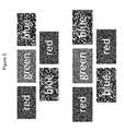
- a light emitting surface with different pixelsThere are three types of pixels, each emitting one color: red, blue or green.
- the display coloris constructed from the combination of the three (red, blue and green) colors.
- the eyehuman views the surface directly through a magnifying lens and thus sees the image.
- the imagecould change with time to display moving objects and the like.
- the firstrelates to a display such as TV, computer screen and the like, and the other is to an electronic projector.
- FIG. 4An illustration of how a chip of the image display device could be partitioned is shown in FIG. 4 to create a system on a chip (SOC).
- the video image from the LED arrayis focused through a lens and is viewed either directly as in a head mounted display or is projected onto a screen
- the plurality of NWLOFscomprises at least a first active region for emitting a first color, a second active region for emitting a second color, and a third active region for emitting a third color.
- the image displaydoes not include a color filter.
- the image display devicecould have three chips to produce red, green and blue and the light, respectively, from each chip and to be interleaved by an external circuit and optical system.
- Each chipmay only consist of a single color array of LEDs for the ease of manufacturing.
- the plurality of NWLOFscomprises at least a first electrical parameter to control emission of the first color, a second electrical parameter to control emission of the second color, and a third electrical parameter to control emission of the third color.
- the image displaycomprises a display device, a microdisplay, a computer display, TV and a display system on a chip.
- Such a devicecould be a system on a chip (SoC) made on a silicon substrate, for example.
- SoCsystem on a chip
- the display(such as that shown in FIG. 4 ) could be a self contained display device that has the following circuits: a NWLOF grid; a row column addressing circuitry; a video signal processing chain for the photodiode array; a feedback loop circuitry for the bias circuits of the nanowire LED; power supplies and regulation circuits; digital circuits to decode standard video signals; and a thermally sound design that would allow for the management of all heat generated by the device.
- FIG. 2illustrates a cross sectional diagram of the devices used in creating the sensor of the present invention. This is the result of integration of an active pixel sensor (APS) architecture typically fabricated in CMOS technology with a pinned photodiode device (item 12 PPD in FIG. 2 ) using a mixed process technology.
- APSactive pixel sensor
- PPDpinned photodiode device
- the uniformity of the photodiode arrayis first ensured by dark and uniform illumination of the entire array with an external source while the nano wire LEDs are turned off.
- the gains, the black levels of the three color channels, and whatever other controls available in the circuitsare then adjusted to their initial values.
- the pixel to pixel uniformity of the LED arrayis ensured by setting the loop gain values of the photodiode/LED pair either individually or in mapped groups through an initial calibration process.
- the LED outputwill retain immunity to temperature variation to the degree that the pinned photodiode allows.
- this approachwill mitigate the development of non-uniformity and local or global drift in brightness, including fixed pattern noise due to manufacturing non-uniformity, in the display generated by the LED array during operation.
- the entire processing, memory, control, and driver systemmay be generally referred to as a controller.
- Various other types of circuitrymay also act as the controller, and the embodiment is not limited to a particular circuitry used.
Landscapes
- Led Devices (AREA)
- Light Receiving Elements (AREA)
- Led Device Packages (AREA)
- Physics & Mathematics (AREA)
- Electromagnetism (AREA)
Abstract
Description
- None.
- PCT International Publication WO 2008/079076, published on Jul. 3, 2008, shows that nanowires can be used for constructing light emitting diodes (LED). Nano-structured LEDs produce light with very high efficiency. They provide a wide range in the choice of materials thereby allowing access to a wide range of wavelengths including red, green and blue light. It is well known, however, that PIN junction LEDs have a light output and wavelength that varies with temperature. Thus, even though the concept of an LED television (TV) is known, the practical application of LEDs for TV has not hitherto been possible.
FIG. 1 is a schematic of a nanowire-containing light emitting diode (LED) with optical feedback.FIG. 2 is a schematic of a pinned photodiode.FIG. 3 is a schematic of tessellations for the LED array.FIG. 4 is a schematic of a chip partitioned to include the LED array and optical feedback.- In the following detailed description, reference is made to the accompanying drawings, which form a part hereof. In the drawings, similar symbols typically identify similar components, unless context dictates otherwise. The illustrative embodiments described in the detailed description, drawings, and claims are not meant to be limiting. Other embodiments may be utilized, and other changes may be made, without departing from the spirit or scope of the subject matter presented here.
- The term nanowire refers to a structure that has a thickness or diameter of the order of several nanometers, for example, 100 nanometers or less and an unconstrained length. An active nanowire is generally capable of converting photons into excitons. Nanowires could exhibit aspect ratios (length-to-width ratio) of 1000 or more. As such they could be referred to as 1-dimensional materials. Nanowires could have many interesting properties that are not seen in bulk or 3-D materials. This is because electrons in nanowires could be quantum confined laterally and thus occupy energy levels that could be different from the traditional continuum of energy levels or bands found in bulk materials. As a result, nanowires could have discrete values of electrical and optical conductance. Nanowires could include metallic (e.g., Ni, Pt, Au), semiconducting (e.g., Si, InP, GaN, etc.), and insulating (e.g., SiO2,TiO2) materials. Molecular nanowires are composed of repeating molecular units either organic or inorganic. Examples of nanowires include inorganic molecular nanowires (Mo6S9-xIx, Li2Mo6Se6), which could have a diameter of 0.9 nm, and can be hundreds of micrometers long. Other examples are based on semiconductors such as InP, Si, GaN, etc., dielectrics (e.g. SiO2,TiO2), or metals (e.g. Ni, Pt). An active-pixel sensor (APS), also commonly written active pixel sensor, is an image sensor consisting of an integrated circuit containing an array of pixel sensors, each pixel containing a photodetector and an active amplifier. A passive-pixel sensor is a pixel sensor without its own amplifier.
- The term excitons refers to electron-hole pairs.
- An active element is any type of circuit component with the ability to electrically control electron and/or hole flow (electricity controlling electricity or light, or vice versa). Components incapable of controlling current by means of another electrical signal are called passive elements. Resistors, capacitors, inductors, transformers, and even diodes are all considered passive elements. Active elements include in embodiments disclosed herein, but are not limited to, an active nanowire, an active waveguide, transistors, silicon-controlled rectifiers (SCRs), light emitting diodes, and photodiodes.
- A waveguide is a system or material designed to confine and direct electromagnetic radiation of selective wavelengths in a direction determined by its physical boundaries. Preferably, the selective wavelength is a function of the diameter of the waveguide. An active waveguide is a waveguide that has the ability to electrically control electron and/or hole flow (electricity controlling electricity or light, or vice versa). This ability of the active waveguide, for example, is one reason why the active waveguide could be considered to be “active” and within the genus of an active element.
- An optical pipe is an element to confine and transmit an electromagnetic radiation. The optical pipe can include a core and a cladding. The core could be a nanowire. The optical pipe could be configured to separate wavelengths of an electromagnetic radiation beam at a selective wavelength through the core and the cladding, wherein the core is configured to be both a channel to transmit the wavelengths up to the selective wavelength and an active element to detect the wavelengths up to the selective wavelength transmitted through the core. A core and a cladding are generally complimentary components of the optical pipe and are configured to separate wavelengths of an electromagnetic radiation beam at a selective wavelength through the core and cladding.
- A photogate is a gate used in an optoelectronic device. Typically the photogate comprises a metal-oxide-semiconductor (MOS) structure. The photogate controls the accumulation of photons generated charges during the integration time of the photodiode and controls the transfer of charges when integration is over. A photodiode comprises a pn junction, however, a photogate can be placed on any type semiconductor material. A vertical photogate is a new structure. Normally, photogates are placed horizontally on planar photodiode devices. In a nanowire device, however, the photogate can be formed in a vertical direction. That is, the photogate can be oriented standing up covering the lateral surface of the nanowire.
- A transfer gate is a gate of a switch transistor used in a pixel. The transfer gate's role is to transfer the charges from one side of a device to another. In some embodiments, the transfer gate is used to transfer the charges from the photodiode to the sensing node (or floating diffusion).
- A reset gate is a gate used for resetting a device. In some embodiments, the reset gate is the sense node that is formed by an n+ region. Reset means to restore to original voltage level set by a certain voltage. In some embodiments, the voltage of the reset drain (RD) is the voltage used as a reset level. Reset means to clear any pending errors or events and bring a system to normal condition or initial state, usually in a controlled manner. Rest is usually done in response to an error condition or completion of events when it is impossible or undesirable for a processing activity to proceed. The ability for an electronic device to be able to reset itself in case of error, abnormal power loss or completion of events could be an aspect of embedded system design and programming.
- An intrinsic semiconductor, also called an undoped semiconductor or i-type semiconductor, is a pure semiconductor without any significant dopant species present. The number of charge carriers is therefore determined by the properties of the material itself instead of the amount of impurities. In intrinsic semiconductors, the number of excited electrons and the number of holes are equal: n=p. The conductivity of intrinsic semiconductors can be due to crystal defects or to thermal excitation. In an intrinsic semiconductor, the number of electrons in the conduction band is equal to the number of holes in the valence band.
- A SOC (system on a chip) is a single integrated circuit, i.e., a processor, a bus, and/or other elements on a single monolithic substrate. A system on a chip may include a configurable logic unit. The configurable logic unit may include a processor, interface, and a programmable logic on the same substrate. A system-on-chip IC may include various reusable functional blocks, such as microprocessors, interfaces, memory arrays, and DSPs (digital signal processors). Such pre-designed functional blocks are commonly called cores. Generally, the SOC may include a plurality of cores in a single chip. The cores embedded in the SOC may be separately designed and tested before being combined in a chip. SOCs may have significant advantages over electronic systems created on boards with discrete components. An integrated circuit having an SOC is generally much smaller than a circuit board based system. The reduction in size afforded by SOCs also may lead to improvements in power consumption and device speed. SOCs may combine fixed and programmable intellectual property cores with custom logic and memory, connected through a bus, on a single piece of silicon, thereby greatly reducing its overall cost.
- A chip is a semiconducting material (usually silicon) on which an integrated circuit is embedded. A typical chip can contain millions of electronic components (transistors). There are different types of chips. For example, CPU chips (also called microprocessors) contain an entire processing unit, whereas memory chips contain blank memory.
- An integrated circuit (also known as IC, microchip, silicon chip, computer chip or chip) is a device that may include many electronic components (transistors, capacitors, resistors, diodes, and other circuit components). These components are often interconnected to form multiple circuit components (e.g., gates, cells, memory units, arithmetic units, controllers, decoders, etc.) on the IC. An example of an integrated circuit is a central processing unit (CPU) in a computer. An integrated circuit may implement one or more cores that perform the various functions of the integrated circuit as well as circuitry for communicating with other integrated circuits and devices external to the integrated circuit. Integrated circuits typically comprise a semiconductor substrate on which several component layers have been formed to produce a large number of laterally-distributed transistors and other circuit devices. Additional connection layers may be formed on top of the component layers to provide interconnections among and power to the circuit devices, and input and output signal connections to the devices. An integrated circuit is generally fabricated utilizing a chip of silicon or other semiconductor material, also referred to as a die. The die consists of a substrate composed of a semiconductor material such as silicon or germanium. One side of the substrate may be provided with a plurality of circuit structures that makeup the integrated circuit and the other may be left as relatively bare substrate material that is normally planarized via a polishing step. A die is typically installed in a package, and electrically connected to leads of the package. A hybrid integrated circuit is a miniaturized electronic circuit constructed of individual semiconductor devices, as well as passive components, bonded to a substrate or circuit board. Integrated circuits can be classified into analog integrated circuits, digital integrated circuits and mixed signal integrated circuits (both analog and digital on the same chip).
- A digital signal processor (DSP) is a specialized microprocessor designed specifically for digital signal processing such as video signal processing, generally in real-time computing. Digital signal processing algorithms typically require a large number of mathematical operations to be performed quickly on a set of data. Signals are converted from analog to digital, manipulated digitally, and then converted again to analog form.
- A PN junction is a junction formed by combining p-type and n-type semiconductors together in very close contact. A PIN junction is a junction formed by combining a lightly doped ‘near’ intrinsic semiconductor region between a p-type semiconductor and an n-type semiconductor regions. The p-type and n-type regions are typically heavily doped because they are used for ohmic contacts.
- The term junction refers to the region where the two regions of the semiconductor meet. It can be thought of as the border region between the p-type and n-type blocks.
- An embodiment relates to a nanostrucuted LED with an optical feedback comprising a substrate, a nanowire protruding from a first side the substrate, an active region to produce light, a optical sensor and a electronic circuit, wherein the optical sensor is configured to detect at least a first portion of the light produced in the active region, and the electronic circuit is configured to control an electrical parameter that controls a light output of the active region. The nanostructured LED in one example implementation, may further comprise a volume element epitaxially connected to the nanowire. The volume element could provide a high doping degree for the formation of the active region, typically within or close to the nanowire, with or without requiring the nanowire itself to be doped. Preferably, the nanostructured LED without optical feedback would be the combination of the substrate, the nanowire and a volume element, wherein a portion of the nanowire and a portion of the volume element are configured to form the active region. The volume, element could be a cylindrical bulb, but is not limited to a cylindrical bulb with a dome-shaped top, a spherical/ellipsoidal, and pyramidal. The volume element can extend in three dimensions; can have a large volume, and a large surface. The volume element/nanowire architecture enhances both electrical and optical performance of a LED. By using different material compositions in the nanowire and the volume element, the nanowire material composition can be chosen to propagate into the volume element in order to decrease the optical disturbance by the connection with the nanowire.
- The nanostructured LED of an embodiment may include a PN or PIN junction that could produce an active region to produce light within the structure during use. The nanowire, a part of the nanowire, or a structure in connection with the nanowire, could form a waveguide directing at least a portion of the light produced in the active region in a given direction.
- The nanowire and the volume element could be embedded in a low index material like SiO2. In one possible implementation the low index region (e.g., a cover layer) is in turn enclosed by a cylindrical ring of metal to provide optical isolation of the each LED from its neighbors. This metal ring may also aid in the local removal of heat generated by each LED.
- A nano-structured LED makes it possible to use a very large fraction of the light produced by the LED. This is at least partly achieved by the nanowire being used as a waveguide, directing the light produced in the junction out of the surface.
- The use of the nanowire as a waveguide offers a possibility to direct light in well defined directions. By using concepts from the area of fiber optics light beams can be focused, or dispersed, depending on the intended use. In this case a concave surface on the nanowire and the silica surrounding it would help provide a focused beam of light suitable for a display system.
- The nanowire technology offers possibilities in choices of materials and material combinations not possible in conventional bulk layer techniques. This could be used in the nano-structured LED to provide LEDs producing light in wavelength regions not accessible by conventional techniques, for example violet and UV.
- The nano-structured LED allows for inclusions of heterostructures as well as areas of different doping within the nanowire, facilitating optimization of electrical and/or optical properties.
- In embodiments herein that require precise control of the light output of an LED or the uniformity of multiple LEDs, arranged in a two dimensional grid for display purposes, an optical feedback loop to create a uniformity of light emission is highly desirable. Such a feedback loop would include an optical sensor to measure a fraction of the light output of the LED in real time and an electronic circuit to use the measurement to adjust the operating point of the LED.
- An embodiment could include a nano-structured LED grown on a substrate that already has an embedded photodiode such as pinned photodiode. The light from the nano-structured LED is partially transmitted to the substrate where a photodiode measures and provides a signal proportional to the intensity of the light generated by the LED. This signal in turn is used in a feedback loop to control the bias point of the LED such that a stable light output is maintained at the desired intensity.
- The nanowire-containing LED with optical feedback (NWLOF) could further comprise a partially reflective layer on the substrate surrounding and/or within the nanowire, wherein the partially reflective layer is configured to allow a first portion of the light to transmit through the partially reflective layer to the optical sensor and to allow at least a second portion of the light to reflect from a surface of the partially reflective layer.
- The NWLOF could further comprise one or more cladding layers surrounding the nanowire, wherein the one or more cladding layers are configured such that the nanowire is configured to form a waveguide. The NWLOF could further comprise a low-index material having a lower refractive index surrounding the nanowire and a metal layer surrounding the low-index material.
- The NWLOF could further comprise a volume element, wherein a portion of the nanowire and a portion of the volume element are configured to form the active region.
FIG. 1 provides an example implementation of this concept. The LED could be composed of the p region in the substrate over which it is grown, the intrinsic nanowire made out of any of the suitable materials listed above and an n type epitaxial region surrounding and contacting the nanowire. A photodiode is embedded into the substrate on which the nanowire is grown. An example of a pinned photodiode is illustrated inFIG. 2 .- In embodiments herein, there are a variety of possible implementations of photodiodes and nano-structured LEDs.
FIG. 1 is an example implementation. Another possible implementation (not shown inFIG. 1 ) would place the LED on the back side of the substrate containing the photodiode. This would require thinning the substrate such that photons from the LED can easily be collected by the potential well (the n+ region inFIG. 1 ) of the photodiode. - A nanostructured LED according to the embodiments comprises of an upstanding nanowire. For the purpose of this application an upstanding nanowire should be interpreted as a nanowire protruding from the substrate in some angle, the upstanding nanowire for example being grown from the substrate, preferably by as vapor-liquid-solid (VLS) grown nanowires. The angle with the substrate will typically be a result of the materials in the substrate and the nanowire, the surface of the substrate and growth conditions. By controlling these parameters it is possible to produce nanowires pointing in only one direction, for example vertical, or in a limited set of directions. For example nanowires and substrates of zinc-blende and diamond semiconductors composed of elements from columns III, V and IV of the periodic table, such nanowires can be grown in the [111] directions and then be grown in the normal direction to any {111} substrate surface. Other directions given as the angle between normal to the surface and the axial direction of the nanowire include 70,53° {111}, 54,73° {100}, and 35,27° and 90°, both to {110}. Thus the nanowires define one, or a limited set, of directions.
- According to the embodiments, a part of the nanowire or structure formed from the nanowire could be used as a waveguide directing and confining at least a portion of the light created in {in or from/out of?} the nanostructured LED in a direction given by the upstanding nanowire. The waveguiding nanostructured LED structure could include a high refractive index nanowire with one or more surrounding cladding with refractive indices less than that of the core. The structure could be either circular symmetrical or close to being circular symmetrical. Light waveguiding in circular symmetrical structures are well know for fiber-optic applications and many parallels can be made to the area of rare-earth-doped fiber optic devices. However, one difference is that fiber amplifier are optically pumped to enhance the light guided through them while the described nanostructured LED can be seen as an efficient light to electricity converter and vice versa.
- Preferably, an output of the optical sensor is an input to the electronic circuit. Preferably, the electrical parameter comprises voltage or current. Preferably, the electronic circuit is configured to control voltage or current such that the light output is maintained substantially constant irrespective of a temperature of the active region within an operating temperature range of the active region. Preferably, the optical sensor comprises a pn or p-i-n photodiode having a performance characteristic that is substantially insensitive to a temperature in an operating temperature range of the active region. Preferably, at least a portion of the light produced in the active region is directed in a direction given by the nanowire. Preferably, the nanowire is configured to both produce light and form a waveguide.
- Preferably, the volume element comprises a doping layer configured to provide a p or n region and a well layer. Preferably, the optical sensor comprises a pinned photodiode in the substrate. Preferably, the one or more cladding layers are configured to provide a graded refractive index such that a refractive index of the nanowire is higher than that of the one or more cladding layer. Preferably, the NWLOF comprises a plurality of the nanowires comprising different materials emit different ranges of wavelengths of the light. Preferably, the NWLOF comprises a plurality of the nanowires comprising different diameters that form waveguides for different ranges of wavelengths of the light. Preferably, the NWLOF comprises a plurality of the nanowires comprising different materials emit different ranges of wavelengths of the light and the NWLOF comprises a plurality of the nanowires comprising different diameters that form waveguides for different ranges of wavelengths of the light. Preferably, the nanowire and the volume element are arranged to direct the light through the nanowire and the substrate such that the light is emitted from a second side of the substrate opposite the first side. Preferably, The substrate contains a photodiode that is optically coupled to the nanowire. Preferably, the volume element is configured to spread the light by dispersion at a junction between the nanowire and the volume element. Preferably, the electronic circuit comprises a controller configured to calibrate the electrical parameter. Preferably, the controller comprises memory, the memory comprising values for controlling the electrical parameter so that the light output is set by the values stored in the memory. Preferably, the controller comprises memory; wherein the controller is configured to calibrate the electrical parameter to cause the light output to more closely match a target output based on target values of the light output stored in the memory. Preferably, the target values represent current values for different colors of the light. Preferably, the target values represent target brightness levels.
- The waveguiding properties of the nanowire can be improved in different ways. The nanowire could have a first effective refractive index, nw, and a cladding surrounding at least a portion of the nanowire could have a second effective refractive index, nc, and by assuring that the first refractive index is larger than the second refractive index, nw>nc, good wave-guiding properties could be provided to the nanowire. The waveguiding properties may be further improved by introducing an optically active cladding.
- The high index material in the nanowire could, for example, be silicon nitride having a refractive index of about 2.0. The lower index cladding layer material could, for example, be a glass, for example a material selected from Table I, having a refractive index about 1.5.
TABLE I Typical Material Index of Refraction PESiN 2.00 PESiO 1.46 SiO2 1.46 In Table I, PESiN refers to plasma enhanced Si3N4and PESiO refers to plasma enhanced SiO2. - For a LED operating in different wavelengths from the visible to the IR and deep in the micrometer wavelengths, a variety of materials can be used, such as: Si, GaAs (p), InAs, Ge, ZnO, InN, GaInN, GaN AlGaInN, InP, InAsP, GaInP, InGaP:Si, InGaP:Zn, GaInAs, AlInP, GaAlInP, GaAlInAsP, GaInSb, InSb among others. To create CMOS circuits, Si and doped Si materials are preferable.
- In one embodiment, the typical values of the refractive indexes for III-V semiconductor nanowire material are in the range from 2.5 to 5.5 when combined with glass type of cladding material (such as SiO2or Si3N4) having refractive indexes ranging from 1.4 to 2.3, satisfying the waveguiding requirement, nw>nc.
- One consideration in the optimization of light extraction is to make the Numerical Aperture (NA) vary along the nanowire structure to optimize light extraction from the structure. In general, it is ideal to have the NA be highest when the light generation takes place furthest away from the exit location. This will maximize the light captured and guided toward the exit. In contrast, closer to the exit end of the structure, the NA can be made smaller since light generated will radiate in random directions and most of the radiate light will hit the top and side of the top part of the structure and exit. Having a lower NA in the top part of the structure also minimizes the light captures and guide back down through the structure that may not be ideal unless a reflector is inserted in the bottom of the structure. A low NA can be obtained by surrounding the III-V nanowire core with another cladding of different composition with slightly less refractive index.
- A nanostructured LED according to the embodiments could comprise a substrate and a nanowire epitaxially grown from the substrate in a defined angle θ. A portion of the nanowire is enclosed by a volume element. The volume element is preferably epitaxially connected to the nanowire. A portion of or all of the nanowire could be arranged to act as a waveguiding portion directing at least a portion of the impinging light in a direction given by the elongated direction of the nanowire, and will be referred to as a waveguide. The nanowire could have a diameter in the order of 50 nm to 500 nm. The length of the nanowire could be of the order of 1 to 10 μm. The pn-junction results in an active region arranged in the nanowire.
- The materials of the different members of the nanostructured LED are chosen so that the nanowire will have good waveguiding properties vis-a-vis the surrounding materials, i.e. the refractive index of the material in the nanowire should preferably be larger than the refractive indices of the surrounding materials.
- If the nanowire has a first refracting index, nw, the material surrounding the nanowire in wave guide portion, typically a cover layer, a second refractive index, nc, and the a volume element, a third refractive nve, then nw>ncand nw>nve. Typical values for the nanostructured LED are nw˜4, nc˜1.5 and nve˜3.
- In addition, the nanowire may be provided with one or more layers. A first layer may be introduced to improve the surface properties (i.e., reduce charge leakage) of the nanowire. Further layers, for example an optical layer may be introduced specifically to improve the waveguiding properties of the nanowire, in manners similar to what is well established in the area of fiber optics. The optical layer typically has a refractive index in between the refractive index of the nanowire and the surrounding cladding region material. Alternatively the intermediate layer has a graded refractive index, which has been shown to improve light transmission in certain cases. If an optical layer is utilized, the refractive index of the nanowire, nw, should define an effective refractive index for both the nanowire and the layers.
- The ability to grow nanowires with well defined diameters could be to optimize the waveguiding properties of the nanowire with regards to the wavelength of the light confined in the nanostructured LED. The diameter of the nanowire could be chosen so as to have a favorable correspondence to the wavelength of the desired light. Preferably the dimensions of the nanowire are such that a uniform optical cavity, optimized for the specific wavelength of the produced light, is provided along the nanowire. The nanowire generally is sufficiently wide to capture the desired light. A rule of thumb would be that diameter must be larger than λ/2nw, wherein λ is the wavelength of the desired light and nwis the refractive index of the nanowire. As an example a diameter of about 60 nm may be appropriate to confine blue light only and one 80 nm may be appropriate for to confine both blue and green light in a silicon nanowire.
- In the infrared and near infrared a diameter above 100 nm would be sufficient. An approximate preferred upper limit for the diameter of the nanowire is given by the growth constrains, and could be in the order of 500 nm. The length of the nanowire is typically and preferably in the order of 1-10 μm, providing enough volume for the active region.
- A reflective layer could be in one embodiment, provided on the substrate and extending under the wire. The reflective layer is preferably provided in the form of a multilayered structure comprising repeated layers of silicates for example, or as a metal film.
- An alternative approach to getting a reflection in the lower end of the nanowire could be to arrange a reflective layer in the substrate underneath the nanowire. Yet another alternative could be to introduce reflective means within the waveguide. Such reflective means can be a multilayered structure provided during the growth process of the nanowire, the multilayered structure comprising repeated layers of for example SiNx/SiOx(dielectric) or GaAs/AlGaAs (semiconductor). Such repeated layers with controlled thickness could also serve as optical grating filters to precisely control the output wavelength of the LED to mitigate wavelength drift for example with temperature.
- In a further embodiment, a major part of the produced light is directed by the waveguide of the nanowire in a downward direction through the substrate. The light can be directed through the entire thickness of the substrate, or alternatively the substrate could be provided with a cut out beneath the base of the nanowire in order to reduce the thickness of the substrate and thereby reduce the scattering or absorption of light in the substrate. The substrate is preferably made of transparent material. A portion, or preferably the entire outer surface of the volume element may be covered by a reflective layer that increases the radiation of the produced light through the waveguide. The reflective layer, for example formed of a metal, may additionally serve as a contact. Part of the nanowire and the substrate could optionally covered by a protective layer of SiC or SiN, for example.
- In an embodiment, the volume element can be arranged to be a dispersive element, giving a light radiation that is essentially evenly distributed over a wide angle. Such device can be well suited for illuminating purposes wherein an even illumination is required. The active region may be arranged in the nanowire but alternatively may be within the volume element, and above the upper end of the nanowire, or radially outwards of the nanowire and possibly above. The nanowire should preferably at its lower end be provided with some of the reflective means, for example a reflective material within the nanowire, in order to redirect light upwards. The geometry of the volume element can be designed to further disperse the light. Dispersion is provided at the junction between the nanowire waveguide and the volume element and further at the edge formed by the upper boundary of the volume element. The height and width of the volume element can be chosen so that the edge disperses light further. One embodiment can be optimized for providing a collected and directionally oriented beam. The nanowire of relatively large diameter, preferably above 150 nm, can extend to the upper surface of the volume element. The nanowire can be provided with a concave lens like exit surface on the upper end.
- Nanowires, acting as waveguides, can be used to improve the performance of conventional planar LEDs. In an embodiment, a plurality of nanowires can be arranged on the surface of a planar LED. Light is produced in the active region, which could be au active layer of the planar LED, for example of GaAsP. The nanowires can be epitaxially connected on top of the planar LED layers in order to get a good matching of the different parts. The nanowires may be coated by a cladding layer protecting the nanowires and/or improving the properties, for example Si3N4. The surface in between the nanowires can be preferably coated with a reflective layer, for example of Au. At least a part of the light, produced in the active region, could enter the nanowires that are acting as waveguides and leading the light away from the substrate plane.
- Depending on the intended use of the nanostructured LED, availability of suitable production processes and cost for materials etc., a wide range of materials can be used for the different parts of the structure. Suitable materials for LED have to be matched with suitable materials for the photo diodes based on the wavelength of the light being emitted/detected by the system. Both the LED and the photo diode should work as intended in the wavelength range of light for which the system is configured to operate.
- In addition, the nanowire based technology allows for defect free combinations of materials that otherwise would be impossible to combine. The III-V semiconductors are of particular interest due to their properties facilitating high speed and low power electronics. Suitable materials for the substrate include, but is not limited to: Si, GaAs, GaP, GaP:Zn, InAs, InP, GaN, Al2O3, SiC, Ge, GaSb, ZnO, InSb, SOI (silicon-on-insulator), CdS, ZnSe, CdTe. In the case of the present invention (i.e. for creating display structure in the visible light), a Si substrate is preferred since it embeds a CMOS photodiode underneath the LED. For wavelengths between blue and near IR, Si could be used in the photo diode. For wavelengths outside the range of light detected by Si, such as IR or UV light, it is possible to use GaAs in photodiodes for LED in the range of 800-1500 nm, e.g., 850 nm; and InGaAs/InP in the range 1310-1550 nm.
- Suitable materials for the nanowire include, but is not limited to: Si, GaAs (p), InAs, Ge, ZnO, InN, GaInN, GaN AlGaInN, BN, InP, InAsP, GaInP, InGaP:Si, InGaP:Zn, GaInAs, AlInP, GaAlInP, GaAlInAsP, GaInSb, InSb. For this application the nano wire materials are carefully selected from the list above and the Table 1 below to produce red, green and blue light.
TABLE 1 List of band gaps Band gap (eV) @ Material 
Symbol 300K Silicon Si 1.11 Selenium Se 1.74 Germanium Ge 0.67 Silicon carbide SiC 2.86 Aluminum phosphide AlP 2.45 Aluminium arsenide AlAs 2.16 Aluminium antimonide AlSb 1.6 Aluminium nitride AlN 6.3 Diamond C 5.5 Gallium(III) phosphide GaP 2.26 Gallium(III) arsenide GaAs 1.43 Gallium(III) nitride GaN 3.4 Gallium(II) sulfide GaS 2.5 (@ 295K) Gallium antimonide GaSb 0.7 Indium(III) nitride InN 0.7 Indium(III) phosphide InP 1.35 Indium(III) arsenide InAs 0.36 Zinc oxide ZnO 3.37 Zinc sulfide ZnS 3.6 Zinc selenide ZnSe 2.7 Zinc telluride ZnTe 2.25 Cadmium sulfide CdS 2.42 Cadmium selenide CdSe 1.73 Cadmium telluride CdTe 1.49 Lead(II) sulfide PbS 0.37 Lead(II) selenide PbSe 0.27 Lead(II) telluride PbTe 0.29 Copper(II) oxide CuO 1.2 - The relationship between wavelength and bandgap energy may be obtained from:
- Where E is the energy, v is the frequency, λ is the wavelength of a photon, h is Planck's constant, and c is the Speed of light. For quick calculations, this reduces to
- A stream of photons with a wavelength of 532 nm (green light) would have an energy of approximately 2.33 eV. Similarly, 1 eV would correspond to a stream of infrared photons of wavelength 1240 nm, and so on.
1 eV=8065.5447 cm−1- Possible donor dopants for example include GaP, Te, Se, S, etc, and acceptor dopants for the same material are Zn, Fe, Mg, Be, Cd, etc. It should be noted that the nanowire technology makes it possible to use nitrides such as SiN, GaN, InN and AlN, which facilitates fabrication of LEDs detecting light in wavelength regions not easily accessible by conventional technique. Other combination of particular commercial interest include, but is not limited to GaAs, GaInP, GaAlInP, GaP systems. Typical doping levels range from 1×1018cm−3to 1×1020cm−3.
- The appropriateness of low resistivity contact materials are dependent on the material to be deposited on, but metal, metal alloys, as well as non-metal compounds, like: Al, Al—Si, TiSi2, TiN, W, MoSi2, PtSi, CoSi2, WSi2, In, AuGa, AuSb, AuGe, PdGe, Ti/Pt/Au, Ti/Al/Ti/Au, Pd/Au, ITO (InSnO), etc. and combinations of, e.g., metal and ITO can be used.
- The substrate could be an integral part of the device, since it also contains the photodiodes necessary to detect light that has not been confined to the nanowire. For this application, the substrate in addition also contains standard CMOS circuits to control the biasing, amplification and readout of the LED as well as any other CMOS circuit deemed necessary and useful. The substrate includes substrates having active devices therein. Suitable materials for the substrates include silicon and silicon-containing materials. Generally, each sensor element of the embodiment includes a nanostructured LED structure comprising a nanowire, a cladding enclosing at least a portion of the nanowire, a coupler and two contacts. Similarly, for light in higher wavelengths, GaAs circuitry can be used with the appropriate light emitting materials for those wavelengths.
- In one embodiment, a micro lens could be located on the LED, for example, as shown in
FIG. 1 . The micro lens may comprise any of several optically transparent lens materials that are known in the art. Non-limiting examples include optically transparent inorganic materials, optically transparent organic materials and optically transparent composite materials. Most common are optically transparent organic materials. Typically the lens layers could be formed incident to patterning and reflow of an organic polymer material that has a glass transition temperature lower than the series of color filter layers, if present, or the patterned planarizing layer. Polymeric materials should preferably have a high degree of stability with temperature to act as micro lenses for LEDs since this device needs to perform at high temperatures. The micro lens ofFIG. 1 does not require a new material; simply patterning the clad material to the right shape forms it. - A method of fabricating nanostructured LED is to first grow a nanowire. Part of the nanowire could then be masked and the volume element could be grown selectively. The volume element grows both axially and radial, hence, when the nanowire is masked partly, the nanowire becomes enclosed in the volume element. Appropriate masking materials are e.g. silicon nitride, silicon oxide etc.
- Considering systems where nanowire growth is locally enhanced by a substance, as VLS grown nanowires, the ability to alter between radial and axial growth by altering growth conditions enables the procedure (nanowire growth, mask formation, and subsequent selective growth) and can be repeated to form nanowire/3D-sequences of higher order. For systems where the nanowire growth and selective growth are not distinguished by separate growth conditions it may be better to first grow the nanowire along the length and by different selective growth steps grow different types of 3D regions or volume elements.
- According to the present invention, in order to fabricate a light emitting pn diode/array with active nanowire region(s) formed of GaAs and InGaP, comprises the steps of: Preferably, the substrate could be Si containing the photodiode. Subsequently, to grow a GaAs nano wire, for example, one could lay down an epitaxial layer of p+ GaP on the silicon substrate.
- 1. Defining of local catalyst/catalysts on a p+ GaP substrate by lithography.
- 2. Growing GaAs nanowire from local catalyst. The growth parameters adjusted for catalytic wire growth.
- 3. Radial growing of thin InGaP concentric layer around the nanowire (cladding layer).
- 4. Depositing of SiO2as mask material.
- 5. Back etching of mask to open up the upper parts of the nanowires.
- 6. Selective growing of n+ InGaP volume element. The growth parameters adjusted to give radial growth.
- 7. Forming contacts on the volume element and to the substrate.
- In the embodiments herein, silicon nanowires (NW) could be grown on a layer of silicon. The process could apply for growing Si NW on dielectric layer, or for III-V compound grown on the appropriate substrate, including Si substrate with or without a thin Molybdenum layer.
- The silicon nanowire of the embodiments disclosed herein could be made as follows. A substrate is provided which comprises silicon having a silicon dioxide surface. The surface can be modified to remove an oxide layer with a surface treatment to promote adsorption of a gold nanoparticle, or gold alloys nanoparticle like AuGa. Onto this modified surface, preferably a Si substrate have the {111} plane, (Au is used to create the Si—Au eutectic point and grow the Si nanowire when SiH4 is introduced), the gold nanoparticle can be formed by deposition of a gold layer, followed by removal of the gold layer over regions other than desired location of the gold nanoparticle. The silicon nanowire can be grown, for example, by plasma enhanced vapor-liquid-solid growth. In a first step, a catalyst particle (typically gold or gold alloy) may be deposited on top of the substrate by either a standard electron beam lithography (EBL) process or using self-assembly of prefabricated catalyst colloids. Other processes for depositing catalysts, such as electroless plating may also be used.
- The diameters of nanowires after growth are generally determined by the area of the catalyst particles. Therefore, a desired diameter of the nanowire can be synthesized by depositing a catalyst particle with an appropriate size. This step typically determines the functionality of the nanowire pixel because the nanowire diameter should be of an appropriate cross-section area to allow the transmission of light with specific wavelengths and long enough to allow the light absorption and creation of excitons (electron-hole pairs).
- A single nanowire can be grown from the catalyst particle under proper conditions. Using silicon as an example, a suitable nanowire can be grown using the vapor-liquid-solid (VLS) process with presence of SiH4at, for example, temperature at 650 C and pressure of 200 mTorr. A temperature below 450 C is advisable for the integration compatibility of CMOS circuits and nanowire synthesis. Many researchers have been able to synthesize silicon nanowires at 430 C or even below 400 C by using some special techniques, for example, using aluminum catalysts or plasma enhanced growth. During the VLS process, the silicon nanowire can be doped to create a p+-i(intrinsic)-n+ structure by introducing B2H6, H2and PH3, respectively.
- Nanowires have a higher surface-to-volume ratio than the corresponding bulk materials. Therefore the surface states of nanowires play a more important role in their electronic and optical properties. The impact of nanowire surface states, however, can be minimized by surface passivation after the nanowire synthesis. Typically, surface passivation can be achieved with a monolayer of materials to react with silicon dangling bonds at the surface of the nanowire. This is accomplished with the formation of stable bonds after reaction. Advantageously, passivation has almost no effect on the nanowire physical dimension since it is only one-monolayer thick.
- Subsequent steps could relate to the forming of an epitaxial layer that is n or p doped covering the nanowire or of one or more of the dielectric layers around the nanowire.
- The epitaxial n or p doped layer covering the nanowire could be grown using vapor-phase epitaxy (VPE), a modification of chemical vapor deposition. Molecular-beam epitaxy, liquid-phase epitaxy (MBE and LPE) and solid-phase epitaxy (SPE) could also be used. In each of these processes, a dopant could be added into the epitaxially grown layer during the epitaxial layer growth process.
- A conformal dielectric coating around the nanowire, if needed, could be made by chemical vapor deposition (CVD), atomic layer deposition (ALD), oxidation or nitration could be made around the nanowire. Then, doped glass dielectric layer could be formed on the conformal dielectric coating by plasma enhanced chemical vapor deposition, spin-on coating or sputtering, optionally with an initial atomic layer deposition. The deposited doped glass dielectric layer could be etched back by chemical-mechanical planarization or other methods of etching.
- In one embodiment, a funnel and a lens on the funnel to channel electromagnetic radiation such as light out of the nanowire waveguide could be made as follows: deposition of a glass/oxide/dielectric layer by CVD, sputter deposition or spin-on coating; application of a photoresist on the deposited glass/oxide/dielectric layer; removal of the photoresist outside an opening centered over the nanowire within the deep cavity; and forming a coupler by semi-isotropic etching in the glass/oxide/dielectric layer.
- Additional steps could relate to the forming of a metal or metal oxide ring layer around the one or more dielectric layers by depositing a metal such a copper on the vertical walls of the one or more dielectric layers.
- The growth process can be varied in known ways to include heterostructures in the nanowires, provide reflective layers etc. The stem in some embodiment can be provided by first growing a thin nanowire, depositing a reflective layer or a selective growth mask covering the lower part, and radial growing a cladding layer or increasing the nanowire thickness.
- The nanowire-containing LEDs with optical feedback could be used in an image display device having a large number of identical display elements, generally greater than 1 million, in a grid. The embodiments disclosed here would allow the manufacture of such a grid of NWLOF.
- In some implementations a large plurality of nanostructured LEDs can be provided in one image display device. A plurality of nanostructured LEDs can be epitaxially grown on a Zn-doped GaP substrate. The nanowires of the LEDs can be of intrinsic GaAs, and provided with a concentric layer of undoped InGaP. The volume elements can comprise of Si-doped InGaP. The lower parts of the nanowires and the substrate can be covered by a SiO2-layer. A back plane contact can be provided on the substrate connecting a plurality of LEDs, and each individual LED can be provided with a wrap around contact on the volume elements. The wrap around contacts can be connected for a group-wise addressing of the LEDs.
- In one embodiment the inherent property that nanowires grow in a limited set of preferred directions, as discussed above, can be used to grown nanowires in the same direction, or one of a limited set of directions. The direction of the grown nanowires could be perpendicular to the substrate or at an angle from the perpendicular to the substrate. Preferably the LEDs can be arranged to produce fairly directed light beams. Adjacent to the group of LEDs a reflective material can be provided, with an angle to the substrate corresponding to the direction of the LEDs so that the light emitted from the LEDs can be reflected by the reflective material in a desired direction.
- Additional features of the image display devices disclosed herein are: (1) A light emitting surface with different pixels. There are three types of pixels, each emitting one color: red, blue or green. The display color is constructed from the combination of the three (red, blue and green) colors. The eye (human) views the surface directly through a magnifying lens and thus sees the image. The image could change with time to display moving objects and the like. (2) There could be the same pixel configuration as in feature (1), but the light emitted from the surface is focused through a lens, and then the final image is displayed on a non-active surface such as a screen. Both cases are viable embodiments. The first relates to a display such as TV, computer screen and the like, and the other is to an electronic projector. An illustration of how a chip of the image display device could be partitioned is shown in
FIG. 4 to create a system on a chip (SOC). The video image from the LED array is focused through a lens and is viewed either directly as in a head mounted display or is projected onto a screen - Preferably, the plurality of NWLOFs comprises at least a first active region for emitting a first color, a second active region for emitting a second color, and a third active region for emitting a third color. Preferably, the image display does not include a color filter.
- Optionally, the image display device could have three chips to produce red, green and blue and the light, respectively, from each chip and to be interleaved by an external circuit and optical system. Each chip may only consist of a single color array of LEDs for the ease of manufacturing.
- Preferably, the plurality of NWLOFs comprises at least a first electrical parameter to control emission of the first color, a second electrical parameter to control emission of the second color, and a third electrical parameter to control emission of the third color. Preferably, the image display comprises a display device, a microdisplay, a computer display, TV and a display system on a chip.
- According to embodiments herein, it is possible to manufacture a device that has other complex circuits besides the NWLOF. Such a device could be a system on a chip (SoC) made on a silicon substrate, for example.
- For example, the display (such as that shown in
FIG. 4 ) could be a self contained display device that has the following circuits: a NWLOF grid; a row column addressing circuitry; a video signal processing chain for the photodiode array; a feedback loop circuitry for the bias circuits of the nanowire LED; power supplies and regulation circuits; digital circuits to decode standard video signals; and a thermally sound design that would allow for the management of all heat generated by the device. Once this SoC is accomplished, it would now be possible to design a single chip display system that requires nothing other than a lens to operate as display SoC. - These are the major circuit blocks required for a display chip:
- 1) A nano wired LED array in a tessellation described in
FIG. 3 . - 2) Row column decode circuitry to individually address an LED and its associated photodiode or to a mapping of a group of contiguous LEDs to a single photodiode.
- 3) A major analog circuit block to provide the Video Signal Processing Chain for read out of photodiode array to provide the input to the controller circuit, the controller circuit itself being for stabilizing the light output of the LED array individually or in groups, power supplies and regulators for the LED array and the photodiode array.
- 4) A digital video decoding circuit to convert standard video input into a form necessary for all other circuits to operate in the chip.
- 5) Memory blocks, both dynamic and static, to be used as video data buffers and program storage.
- 6) Microprocessor, which is optional, could be included to carry out any of the functions capable of a microprocessor.
- 1) A nano wired LED array in a tessellation described in
- With the appropriate choice of materials for the nano-wire, the epitaxial layer and the diameter of the nanowire, Red, Green and Blue LEDs can be implemented. The preferred tessellations for the LED array is shown in
FIGS. 3( a) and3(b). There are a number of other possible arrangements, for example: R G B R G B R G B R G B R G B R G B R G B R G B B G R B G R B G R B G R B G R B G R B G R B G R R G B R G B R G B R G B R G B R G B R G B R G B - The pinned photodiode shown in
FIG. 2 is described in U.S. Pat. No. 6,100,551, which is incorporated herein in their entirety by reference.FIG. 2 illustrates a cross sectional diagram of the devices used in creating the sensor of the present invention. This is the result of integration of an active pixel sensor (APS) architecture typically fabricated in CMOS technology with a pinned photodiode device (item 12 PPD inFIG. 2 ) using a mixed process technology. The PPD becomes the photoactive element in an XY-addressable area array. - The uniformity of the photodiode array is first ensured by dark and uniform illumination of the entire array with an external source while the nano wire LEDs are turned off. The gains, the black levels of the three color channels, and whatever other controls available in the circuits are then adjusted to their initial values. Similarly, the pixel to pixel uniformity of the LED array is ensured by setting the loop gain values of the photodiode/LED pair either individually or in mapped groups through an initial calibration process.
- In subsequent operation the LED output will retain immunity to temperature variation to the degree that the pinned photodiode allows. In addition this approach will mitigate the development of non-uniformity and local or global drift in brightness, including fixed pattern noise due to manufacturing non-uniformity, in the display generated by the LED array during operation.
- The entire processing, memory, control, and driver system may be generally referred to as a controller. Various other types of circuitry may also act as the controller, and the embodiment is not limited to a particular circuitry used.
- All references mentioned in the application are incorporated herein in their entirety by reference.

Claims (43)
Priority Applications (20)
| Application Number | Priority Date | Filing Date | Title |
|---|---|---|---|
| US12/573,582US8791470B2 (en) | 2009-10-05 | 2009-10-05 | Nano structured LEDs |
| TW99133891ATWI470783B (en) | 2009-10-05 | 2010-10-05 | Nanostructured light-emitting diode |
| TW103143553ATW201511247A (en) | 2009-10-05 | 2010-10-05 | Nanostructured light-emitting diode |
| PCT/US2010/051435WO2011044101A1 (en) | 2009-10-05 | 2010-10-05 | Nanostructured leds |
| US12/945,492US9515218B2 (en) | 2008-09-04 | 2010-11-12 | Vertical pillar structured photovoltaic devices with mirrors and optical claddings |
| US13/106,851US9082673B2 (en) | 2009-10-05 | 2011-05-12 | Passivated upstanding nanostructures and methods of making the same |
| US13/925,429US9304035B2 (en) | 2008-09-04 | 2013-06-24 | Vertical waveguides with various functionality on integrated circuits |
| US14/274,448US20140246684A1 (en) | 2009-10-05 | 2014-05-09 | Nano structured leds |
| US14/503,598US9410843B2 (en) | 2008-09-04 | 2014-10-01 | Nanowire arrays comprising fluorescent nanowires and substrate |
| US14/516,402US20160111460A1 (en) | 2008-09-04 | 2014-10-16 | Back-lit photodetector |
| US14/516,162US20160111562A1 (en) | 2008-09-04 | 2014-10-16 | Multispectral and polarization-selective detector |
| US14/632,739US9601529B2 (en) | 2008-09-04 | 2015-02-26 | Light absorption and filtering properties of vertically oriented semiconductor nano wires |
| US14/704,143US20150303333A1 (en) | 2008-09-04 | 2015-05-05 | Passivated upstanding nanostructures and methods of making the same |
| US14/705,380US9337220B2 (en) | 2008-09-04 | 2015-05-06 | Solar blind ultra violet (UV) detector and fabrication methods of the same |
| US15/057,153US20160178840A1 (en) | 2008-09-04 | 2016-03-01 | Optical waveguides in image sensors |
| US15/082,514US20160211394A1 (en) | 2008-11-13 | 2016-03-28 | Nano wire array based solar energy harvesting device |
| US15/090,155US20160216523A1 (en) | 2008-09-04 | 2016-04-04 | Vertical waveguides with various functionality on integrated circuits |
| US15/093,928US20160225811A1 (en) | 2008-09-04 | 2016-04-08 | Nanowire structured color filter arrays and fabrication method of the same |
| US15/149,252US20160254301A1 (en) | 2008-09-04 | 2016-05-09 | Solar blind ultra violet (uv) detector and fabrication methods of the same |
| US15/225,264US20160344964A1 (en) | 2008-09-04 | 2016-08-01 | Methods for fabricating and using nanowires |
Applications Claiming Priority (1)
| Application Number | Priority Date | Filing Date | Title |
|---|---|---|---|
| US12/573,582US8791470B2 (en) | 2009-10-05 | 2009-10-05 | Nano structured LEDs |
Related Parent Applications (1)
| Application Number | Title | Priority Date | Filing Date |
|---|---|---|---|
| US12/575,221Continuation-In-PartUS8384007B2 (en) | 2008-09-04 | 2009-10-07 | Nano wire based passive pixel image sensor |
Related Child Applications (3)
| Application Number | Title | Priority Date | Filing Date |
|---|---|---|---|
| US12/575,221Continuation-In-PartUS8384007B2 (en) | 2008-09-04 | 2009-10-07 | Nano wire based passive pixel image sensor |
| US13/106,851Continuation-In-PartUS9082673B2 (en) | 2008-09-04 | 2011-05-12 | Passivated upstanding nanostructures and methods of making the same |
| US14/274,448ContinuationUS20140246684A1 (en) | 2008-09-04 | 2014-05-09 | Nano structured leds |
Publications (2)
| Publication Number | Publication Date |
|---|---|
| US20110079796A1true US20110079796A1 (en) | 2011-04-07 |
| US8791470B2 US8791470B2 (en) | 2014-07-29 |
Family
ID=43822512
Family Applications (2)
| Application Number | Title | Priority Date | Filing Date |
|---|---|---|---|
| US12/573,582Expired - Fee RelatedUS8791470B2 (en) | 2008-09-04 | 2009-10-05 | Nano structured LEDs |
| US14/274,448AbandonedUS20140246684A1 (en) | 2008-09-04 | 2014-05-09 | Nano structured leds |
Family Applications After (1)
| Application Number | Title | Priority Date | Filing Date |
|---|---|---|---|
| US14/274,448AbandonedUS20140246684A1 (en) | 2008-09-04 | 2014-05-09 | Nano structured leds |
Country Status (3)
| Country | Link |
|---|---|
| US (2) | US8791470B2 (en) |
| TW (2) | TW201511247A (en) |
| WO (1) | WO2011044101A1 (en) |
Cited By (18)
| Publication number | Priority date | Publication date | Assignee | Title |
|---|---|---|---|---|
| US20100148149A1 (en)* | 2006-12-22 | 2010-06-17 | Qunano Ab | Elevated led and method of producing such |
| US20110180894A1 (en)* | 2008-09-04 | 2011-07-28 | Qunano Ab | Nanostructured photodiode |
| EP2924474A1 (en)* | 2014-03-26 | 2015-09-30 | Sick Ag | Optical sensor with a nanostructure-based light-emitting diode comprised in a light transmitter |
| CN105594000A (en)* | 2013-09-30 | 2016-05-18 | 艾利迪公司 | Optoelectronic devices with light emitting diodes |
| CN106444250A (en)* | 2016-10-28 | 2017-02-22 | 江苏新广联半导体有限公司 | Projector module for micro-display with three-typed LEDs |
| WO2017042513A1 (en)* | 2015-09-10 | 2017-03-16 | Aledia | Light-emitting device having a built-in light sensor |
| WO2017042512A1 (en)* | 2015-09-10 | 2017-03-16 | Aledia | Light-emitting device with integrated light sensor |
| US9865714B2 (en)* | 2016-04-06 | 2018-01-09 | International Business Machines Corporation | III-V lateral bipolar junction transistor |
| FR3058570A1 (en)* | 2016-11-10 | 2018-05-11 | Valeo Vision | LIGHT SOURCE WITH LIGHT EMITTING UNITS WITH DETECTION FUNCTION |
| CN109698259A (en)* | 2017-10-20 | 2019-04-30 | 乐金显示有限公司 | Light emitting diode using anisotropy nanometer rods and the light emitting device including it |
| US20190131345A1 (en)* | 2016-09-30 | 2019-05-02 | Intel Corporation | Micro-led displays |
| US20200036443A1 (en)* | 2016-09-29 | 2020-01-30 | The Regents Of The University Of California | Visible light communication locks |
| JP2021512501A (en)* | 2018-02-06 | 2021-05-13 | アレディア | Photoelectronic devices and manufacturing methods with electronic components at the level of the back surface of the substrate |
| WO2021202746A1 (en)* | 2020-04-03 | 2021-10-07 | Magic Leap, Inc. | Wearable display systems with nanowire led micro-displays |
| CN113544826A (en)* | 2019-03-29 | 2021-10-22 | 索尼半导体解决方案公司 | Image forming apparatus with a plurality of image forming units |
| US20230116053A1 (en)* | 2021-09-29 | 2023-04-13 | International Business Machines Corporation | Device integration using carrier wafer |
| CN116682843A (en)* | 2023-08-03 | 2023-09-01 | 浙江大学 | A nanowire light-emitting device and its preparation method |
| CN117038696A (en)* | 2023-08-11 | 2023-11-10 | 浙江大学 | Multi-stage light-emitting branch nanowire light-emitting device and preparation method thereof |
Families Citing this family (19)
| Publication number | Priority date | Publication date | Assignee | Title |
|---|---|---|---|---|
| US8748799B2 (en) | 2010-12-14 | 2014-06-10 | Zena Technologies, Inc. | Full color single pixel including doublet or quadruplet si nanowires for image sensors |
| US8229255B2 (en) | 2008-09-04 | 2012-07-24 | Zena Technologies, Inc. | Optical waveguides in image sensors |
| US9406709B2 (en) | 2010-06-22 | 2016-08-02 | President And Fellows Of Harvard College | Methods for fabricating and using nanowires |
| US9515218B2 (en) | 2008-09-04 | 2016-12-06 | Zena Technologies, Inc. | Vertical pillar structured photovoltaic devices with mirrors and optical claddings |
| US9343490B2 (en) | 2013-08-09 | 2016-05-17 | Zena Technologies, Inc. | Nanowire structured color filter arrays and fabrication method of the same |
| US9000353B2 (en) | 2010-06-22 | 2015-04-07 | President And Fellows Of Harvard College | Light absorption and filtering properties of vertically oriented semiconductor nano wires |
| US8274039B2 (en) | 2008-11-13 | 2012-09-25 | Zena Technologies, Inc. | Vertical waveguides with various functionality on integrated circuits |
| US9299866B2 (en) | 2010-12-30 | 2016-03-29 | Zena Technologies, Inc. | Nanowire array based solar energy harvesting device |
| US8735797B2 (en) | 2009-12-08 | 2014-05-27 | Zena Technologies, Inc. | Nanowire photo-detector grown on a back-side illuminated image sensor |
| US8866065B2 (en) | 2010-12-13 | 2014-10-21 | Zena Technologies, Inc. | Nanowire arrays comprising fluorescent nanowires |
| US9478685B2 (en) | 2014-06-23 | 2016-10-25 | Zena Technologies, Inc. | Vertical pillar structured infrared detector and fabrication method for the same |
| US8299472B2 (en) | 2009-12-08 | 2012-10-30 | Young-June Yu | Active pixel sensor with nanowire structured photodetectors |
| DE102012109460B4 (en)* | 2012-10-04 | 2024-03-07 | OSRAM Opto Semiconductors Gesellschaft mit beschränkter Haftung | Method for producing a light-emitting diode display and light-emitting diode display |
| US9059337B1 (en)* | 2013-12-24 | 2015-06-16 | Christie Digital Systems Usa, Inc. | Method, system and apparatus for dynamically monitoring and calibrating display tiles |
| US10529696B2 (en)* | 2016-04-12 | 2020-01-07 | Cree, Inc. | High density pixelated LED and devices and methods thereof |
| JP6999877B2 (en) | 2017-07-31 | 2022-01-19 | セイコーエプソン株式会社 | Luminous device and projector |
| US10818816B2 (en) | 2017-11-22 | 2020-10-27 | Advanced Semiconductor Engineering, Inc. | Optical device with decreased interference |
| US11011571B2 (en) | 2018-08-24 | 2021-05-18 | Innovation Semiconductor | Nanowire light emitting switch devices and methods thereof |
| US11588081B2 (en)* | 2020-03-04 | 2023-02-21 | Advanced Semiconductor Engineering, Inc. | Semiconductor device package |
Citations (97)
| Publication number | Priority date | Publication date | Assignee | Title |
|---|---|---|---|---|
| US4443890A (en)* | 1980-12-02 | 1984-04-17 | Thomson-Csf | Optical-connection direct-light modulation information transmission system with a passband extended towards the low frequencies and continuous waves |
| US4896941A (en)* | 1985-04-27 | 1990-01-30 | Doryokuro Kakunenryo Kaihatsu Jigyodan | Image-transmitting fiber |
| US5096520A (en)* | 1990-08-01 | 1992-03-17 | Faris Sades M | Method for producing high efficiency polarizing filters |
| US5401968A (en)* | 1989-12-29 | 1995-03-28 | Honeywell Inc. | Binary optical microlens detector array |
| US5602661A (en)* | 1993-02-17 | 1997-02-11 | Hoffmann-La Roche Inc. | Optical component |
| US5612780A (en)* | 1996-06-05 | 1997-03-18 | Harris Corporation | Device for detecting light emission from optical fiber |
| US5723945A (en)* | 1996-04-09 | 1998-03-03 | Electro Plasma, Inc. | Flat-panel display |
| US5877492A (en)* | 1995-09-14 | 1999-03-02 | Nec Corporation | Contact type image sensor comprising a plurality of microlenses |
| US5880495A (en)* | 1998-01-08 | 1999-03-09 | Omnivision Technologies, Inc. | Active pixel with a pinned photodiode |
| US6033582A (en)* | 1996-01-22 | 2000-03-07 | Etex Corporation | Surface modification of medical implants |
| US20020009129A1 (en)* | 2000-06-24 | 2002-01-24 | Samsung Electronics Co., Ltd. | Apparatus and method for synchronization of uplink synchronous transmission scheme in a CDMA communication system |
| US20020021714A1 (en)* | 2000-05-25 | 2002-02-21 | Mitsubishi Denki Kabushiki Kaisha | Data transmission method combating degradation of the quality of service |
| US20020021698A1 (en)* | 2000-04-10 | 2002-02-21 | Yu-Ro Lee | Data transmission method for hybrid ARQ type II/III uplink for a wide-band radio communication system |
| US20020028690A1 (en)* | 2000-08-14 | 2002-03-07 | Vesuvius, Inc. | Communique subscriber handoff between a narrowcast cellular communication network and a point-to-point cellular communication network |
| US20020032884A1 (en)* | 1997-02-18 | 2002-03-14 | Hiroshi Kobata | Robust delivery system |
| US20030003920A1 (en)* | 2001-06-28 | 2003-01-02 | Sebastian Peroor K. | Method and system for adapting a wireless link to achieve a desired channel quality |
| US20030007510A1 (en)* | 2001-07-07 | 2003-01-09 | Lg Electronics Inc. | Method for setting user equipment identifier in radio communication system |
| US20030006363A1 (en)* | 2001-04-27 | 2003-01-09 | Campbell Scott Patrick | Optimization of alignment between elements in an image sensor |
| US20030016672A1 (en)* | 1999-01-19 | 2003-01-23 | Rosen Eric C. | Shared communications network employing virtual-private-network identifiers |
| US20030043741A1 (en)* | 2001-08-31 | 2003-03-06 | Mitsubishi Denki Kabushiki Kaisha | Bandwidth updating method and bandwidth updating apparatus |
| US20030050097A1 (en)* | 2001-09-10 | 2003-03-13 | Shahrokh Amirijoo | Recovery of mobile station(s) in connected mode upon RNC failure |
| US20030054829A1 (en)* | 1999-12-15 | 2003-03-20 | Martti Moisio | Channel allocation method in a cellular radio network |
| US20040002334A1 (en)* | 2002-05-13 | 2004-01-01 | Samsung Electronics Co., Ltd. | Method of performing inter-rat measurement for a handover from NB-TDD to GSM |
| US20040006643A1 (en)* | 2002-06-26 | 2004-01-08 | Sandvine Incorporated | TCP proxy providing application layer modifications |
| US20040004954A1 (en)* | 2002-05-10 | 2004-01-08 | Interdigital Technology Corporation | System and method for monitoring transmission sequence numbers assigned to protocol data units to detect and correct transmission errors |
| US20040008658A1 (en)* | 1998-10-05 | 2004-01-15 | Telefonaktiebolaget L M Ericsson | Random access in a mobile telecommunications system |
| US20040008659A1 (en)* | 2002-07-08 | 2004-01-15 | Samsung Electronics Co., Ltd | Method of setting initial transport format combination in broadband code division multiple access system |
| US20040014452A1 (en)* | 2000-10-17 | 2004-01-22 | Kwang-Jae Lim | Random access channal access apparatus for mobile satellite communication system and method therefor |
| US20040026684A1 (en)* | 2002-04-02 | 2004-02-12 | Nanosys, Inc. | Nanowire heterostructures for encoding information |
| US20040028078A1 (en)* | 2000-10-09 | 2004-02-12 | Mark Beckmann | Method for transmitting data packets via a radio interface of a mobile radio system |
| US6694148B1 (en)* | 1999-07-26 | 2004-02-17 | Telefonaktiebolaget Lm Ericsson (Publ) | Transmit power control for MCPA-equipped based stations |
| US6709929B2 (en)* | 2001-06-25 | 2004-03-23 | North Carolina State University | Methods of forming nano-scale electronic and optoelectronic devices using non-photolithographically defined nano-channel templates |
| US20040057387A1 (en)* | 2002-06-22 | 2004-03-25 | Lg Electronics, Inc. | Multimedia service providing method for radio mobile communication system |
| US20040058058A1 (en)* | 2000-04-12 | 2004-03-25 | Shchegolikhin Alexander Nikitovich | Raman-active taggants and thier recognition |
| US20050008035A1 (en)* | 2001-11-12 | 2005-01-13 | Carl Eklund | Method and device for retransmission of transmitted units |
| US20050014508A1 (en)* | 2000-03-28 | 2005-01-20 | Moulsley Timothy J. | Radio communication system |
| US20050013272A1 (en)* | 1998-10-01 | 2005-01-20 | Lg Electronics Inc. | Method for formatting signal in mobile communication system |
| US20050020260A1 (en)* | 2003-07-11 | 2005-01-27 | Samsung Electronics Co., Ltd. | Apparatus and method for transmitting/receiving MBMS control information in a mobile communication system |
| US6850504B1 (en)* | 1997-10-31 | 2005-02-01 | Lucent Technologies Inc. | Access to communications systems |
| US20050025039A1 (en)* | 2003-07-30 | 2005-02-03 | Samsung Electronics Co., Ltd. | Apparatus and method for assigning subchannel in a mobile communication system using orthogonal frequency division multiple access scheme |
| US20050026623A1 (en)* | 2003-04-17 | 2005-02-03 | Interdigital Technology Corporation | Method for implementing fast-dynamic channel allocation call admission control for radio link reconfiguration in radio resource management |
| US20050039101A1 (en)* | 2001-11-28 | 2005-02-17 | Johan Torsner | Method and system of retransmission |
| US6859445B1 (en)* | 1999-07-07 | 2005-02-22 | Samsung Electronics Co., Ltd. | Channel assignment apparatus and method for a common packet channel in a WCDMA mobile communication system |
| US20050041573A1 (en)* | 2003-07-30 | 2005-02-24 | Samsung Electronics Co., Ltd. | Ranging method in a broadband wireless access communication system |
| US20050054368A1 (en)* | 2003-08-27 | 2005-03-10 | Messay Amerga | Intra-frequency searching in the presence of frequency gaps |
| US20050059421A1 (en)* | 2003-09-16 | 2005-03-17 | Reed John D. | System, method, and apparatus for establishing headroom for a mobile station |
| US20050059407A1 (en)* | 2003-09-15 | 2005-03-17 | Reed John D. | Resource negotiation in wireless communications networks and methods |
| US20050063336A1 (en)* | 2003-09-20 | 2005-03-24 | Samsung Electronics Co., Ltd. | System and mehtod for dynamically allocating resources in a mobile communication system employing orthogonal frequency division multiple access |
| US20050068963A1 (en)* | 2003-09-29 | 2005-03-31 | Lg Electronics Inc. | Method and apparatus for establishing radio bearer for point-to-multipoint multimedia service in mobile communication system |
| US20060007886A1 (en)* | 2004-06-14 | 2006-01-12 | Lg Electronics Inc. | Reducing overheads of a protocol data unit in a wireless communication system |
| US6987258B2 (en)* | 2001-12-19 | 2006-01-17 | Intel Corporation | Integrated circuit-based compound eye image sensor using a light pipe bundle |
| US20060018289A1 (en)* | 2002-09-27 | 2006-01-26 | Matthias Schulist | Requesting and controlling access in a wireless communications network |
| US20060025079A1 (en)* | 2004-08-02 | 2006-02-02 | Ilan Sutskover | Channel estimation for a wireless communication system |
| US6996147B2 (en)* | 2001-03-30 | 2006-02-07 | The Regents Of The University Of California | Methods of fabricating nanostructures and nanowires and devices fabricated therefrom |
| US20060030342A1 (en)* | 2004-04-16 | 2006-02-09 | Samsung Electronics Co., Ltd. | Method for transmitting and receiving control information in a mobile communication system supporting multimedia broadcast/multicast service |
| US20060045047A1 (en)* | 2004-08-27 | 2006-03-02 | Samsung Electronics Co., Ltd. | Random access method in multi-cell OFDMA networks |
| US20060056347A1 (en)* | 2004-09-14 | 2006-03-16 | Samsung Electronics Co., Ltd. | Method and apparatus for indicating cell selection when a session is stopped in a multimedia broadcast/multicast service system |
| US20060059186A1 (en)* | 2001-12-27 | 2006-03-16 | Ingemar Backlund | Method and apparatus relating to retransmission of data between different protocol layers |
| US7016343B1 (en)* | 2001-12-28 | 2006-03-21 | Cisco Technology, Inc. | PSTN call routing control features applied to a VoIP |
| US20060062196A1 (en)* | 2004-08-16 | 2006-03-23 | Sean Cai | Fast cell search and accurate synchronization in wireless communications |
| USRE39454E1 (en)* | 1987-03-17 | 2007-01-02 | Qpsx Communications Pty. Ltd. | Transfer of messages in a multiplexed system |
| US7163659B2 (en)* | 2002-12-03 | 2007-01-16 | Hewlett-Packard Development Company, L.P. | Free-standing nanowire sensor and method for detecting an analyte in a fluid |
| US20070012985A1 (en)* | 2004-03-23 | 2007-01-18 | Nanosys, Inc. | Nanowire capacitor and methods of making same |
| US20070023799A1 (en)* | 2005-08-01 | 2007-02-01 | Micro Technology, Inc. | Structure and method for building a light tunnel for use with imaging devices |
| US20070029545A1 (en)* | 2003-02-24 | 2007-02-08 | Ignis Innovation Inc | Pixel having an organic light emitting diode and method of fabricating the pixel |
| US7184792B2 (en)* | 2004-02-10 | 2007-02-27 | Qualcomm Incorporated | Delayed data transmission in a wireless communication system after physical layer reconfiguration |
| US20070052050A1 (en)* | 2005-09-07 | 2007-03-08 | Bart Dierickx | Backside thinned image sensor with integrated lens stack |
| US20070060146A1 (en)* | 2005-07-20 | 2007-03-15 | Samsung Electronics., Ltd. | System and method for transmitting/receiving resource allocation information in a communication system |
| US20070071025A1 (en)* | 2003-10-06 | 2007-03-29 | Telefonaktiebolaget Lm Ericsson (Publ) | Mbms acknowledgements on rach |
| US20080004054A1 (en)* | 2004-07-27 | 2008-01-03 | Andrea Barbaresi | Transmission of Multimedia Contents to a Plurality of Mobile Users |
| US20080031253A1 (en)* | 2004-05-19 | 2008-02-07 | Soeng-Hun Kim | Apparatus and Method for Efficiently Processing Voice Packet Data in Mobile Communication System Providing Voice Service Using Packet Network |
| US7330404B2 (en)* | 2003-10-10 | 2008-02-12 | Seagate Technology Llc | Near-field optical transducers for thermal assisted magnetic and optical data storage |
| US20080036038A1 (en)* | 2006-03-10 | 2008-02-14 | Hersee Stephen D | PULSED GROWTH OF CATALYST-FREE GROWITH OF GaN NANOWIRES AND APPLICATION IN GROUP III NITRIDE SEMICONDUCTOR BULK MATERIAL |
| US20080044984A1 (en)* | 2006-08-16 | 2008-02-21 | Taiwan Semiconductor Manufacturing Co., Ltd. | Methods of avoiding wafer breakage during manufacture of backside illuminated image sensors |
| US20080043619A1 (en)* | 2006-08-21 | 2008-02-21 | Interdigital Technology Corporation | Method and apparatus for controlling arq and harq transmissions and retransmissions in a wireless communication system |
| US7335962B2 (en)* | 2004-07-08 | 2008-02-26 | Micron Technology, Inc. | Photonic crystal-based lens elements for use in an image sensor |
| US7336860B2 (en)* | 2003-04-07 | 2008-02-26 | Eksigent Technologies, Llc | Microfluidic detection device having reduced dispersion and method for making same |
| US20080047601A1 (en)* | 2006-08-22 | 2008-02-28 | Somnath Nag | High Efficiency Solar Cells and Manufacturing Methods |
| US20080069031A1 (en)* | 2004-06-22 | 2008-03-20 | Nortel Networks Limited | Methods and Systems for Enabling Feedback in Wireless Communication Networks |
| US20080073742A1 (en)* | 2006-09-26 | 2008-03-27 | Adkisson James W | Stacked image package |
| US20090011718A1 (en)* | 2006-01-05 | 2009-01-08 | Sung-Duck Chun | Maintaining Communication Between Mobile Terminal and Network in Mobile Communication System |
| US20090011769A1 (en)* | 2006-01-05 | 2009-01-08 | Sung-Jun Park | Transmitting Information in Mobile Communications System |
| US20090032687A1 (en)* | 2007-08-01 | 2009-02-05 | Silverbrook Research Pty Ltd | Two dimensional contact image sensor with frontlighting |
| US7491269B2 (en)* | 2001-12-04 | 2009-02-17 | Thales | Method for catalytic growth of nanotubes or nanofibers comprising a NiSi alloy diffusion barrier |
| US20090046749A1 (en)* | 2004-08-04 | 2009-02-19 | Kiminori Mizuuchi | Coherent light source |
| US20090050204A1 (en)* | 2007-08-03 | 2009-02-26 | Illuminex Corporation. | Photovoltaic device using nanostructured material |
| US7646138B2 (en)* | 2006-11-21 | 2010-01-12 | Interuniversitair Microelektronica Centrum (Imec) | Diamond enhanced thickness shear mode resonator |
| US7646943B1 (en)* | 2008-09-04 | 2010-01-12 | Zena Technologies, Inc. | Optical waveguides in image sensors |
| US7647695B2 (en)* | 2003-12-30 | 2010-01-19 | Lockheed Martin Corporation | Method of matching harnesses of conductors with apertures in connectors |
| US20100014430A1 (en)* | 2005-01-18 | 2010-01-21 | Matsushita Electric Industrial Co., Ltd. | Resource allocation method and base station device |
| US20100019355A1 (en)* | 2008-07-25 | 2010-01-28 | Theodore I Kamins | Multi-Level Nanowire Structure And Method Of Making The Same |
| US20100019296A1 (en)* | 2008-07-24 | 2010-01-28 | Cha Dae-Kil | Image sensor having nanodot |
| US7655860B2 (en)* | 2005-04-01 | 2010-02-02 | North Carolina State University | Nano-structured photovoltaic solar cell and related methods |
| US20100034095A1 (en)* | 2008-08-08 | 2010-02-11 | Qualcomm Incorporated | Processing polling requests from radio link control peers |
| US7664059B2 (en)* | 2005-04-05 | 2010-02-16 | Innovative Sonic Limited | Error handling in a wireless communications system |
| US20110038376A1 (en)* | 2004-08-31 | 2011-02-17 | Henning Wiemann | Data Unit Sender and Data Unit Relay Device |
| US20110036396A1 (en)* | 2008-04-30 | 2011-02-17 | The Regents Of The University Of California | Method and apparatus for fabricating optoelectromechanical devices by structural transfer using re-usable substrate |
Family Cites Families (345)
| Publication number | Priority date | Publication date | Assignee | Title |
|---|---|---|---|---|
| US1918848A (en) | 1929-04-26 | 1933-07-18 | Norwich Res Inc | Polarizing refracting bodies |
| US3903427A (en) | 1973-12-28 | 1975-09-02 | Hughes Aircraft Co | Solar cell connections |
| US4017332A (en) | 1975-02-27 | 1977-04-12 | Varian Associates | Solar cells employing stacked opposite conductivity layers |
| US4292512A (en)* | 1978-06-19 | 1981-09-29 | Bell Telephone Laboratories, Incorporated | Optical monitoring photodiode system |
| US4357415A (en) | 1980-03-06 | 1982-11-02 | Eastman Kodak Company | Method of making a solid-state color imaging device having a color filter array using a photocrosslinkable barrier |
| US4400221A (en) | 1981-07-08 | 1983-08-23 | The United States Of America As Represented By The Secretary Of The Air Force | Fabrication of gallium arsenide-germanium heteroface junction device |
| US4387265A (en) | 1981-07-17 | 1983-06-07 | University Of Delaware | Tandem junction amorphous semiconductor photovoltaic cell |
| US5696863A (en) | 1982-08-06 | 1997-12-09 | Kleinerman; Marcos Y. | Distributed fiber optic temperature sensors and systems |
| US5247349A (en) | 1982-11-16 | 1993-09-21 | Stauffer Chemical Company | Passivation and insulation of III-V devices with pnictides, particularly amorphous pnictides having a layer-like structure |
| US4678772A (en) | 1983-02-28 | 1987-07-07 | Yissum Research Development Company Of The Hebrew University Of Jerusalem | Compositions containing glycyrrhizin |
| US4513168A (en) | 1984-04-19 | 1985-04-23 | Varian Associates, Inc. | Three-terminal solar cell circuit |
| US4620237A (en) | 1984-10-22 | 1986-10-28 | Xerox Corporation | Fast scan jitter measuring system for raster scanners |
| US4827335A (en) | 1986-08-29 | 1989-05-02 | Kabushiki Kaisha Toshiba | Color image reading apparatus with two color separation filters each having two filter elements |
| EP0275063A3 (en) | 1987-01-12 | 1992-05-27 | Sumitomo Electric Industries Limited | Light emitting element comprising diamond and method for producing the same |
| JPH0721562B2 (en) | 1987-05-14 | 1995-03-08 | 凸版印刷株式会社 | Color filter |
| JPH0288498A (en) | 1988-06-13 | 1990-03-28 | Sumitomo Electric Ind Ltd | Diamond laser crystal and its manufacturing method |
| FR2633101B1 (en) | 1988-06-16 | 1992-02-07 | Commissariat Energie Atomique | PHOTODIODE AND MATRIX OF PHOTODIODES ON HGCDTE AND METHODS OF MAKING SAME |
| US5311047A (en) | 1988-11-16 | 1994-05-10 | National Science Council | Amorphous SI/SIC heterojunction color-sensitive phototransistor |
| US5124543A (en) | 1989-08-09 | 1992-06-23 | Ricoh Company, Ltd. | Light emitting element, image sensor and light receiving element with linearly varying waveguide index |
| US4971928A (en) | 1990-01-16 | 1990-11-20 | General Motors Corporation | Method of making a light emitting semiconductor having a rear reflecting surface |
| US5362972A (en) | 1990-04-20 | 1994-11-08 | Hitachi, Ltd. | Semiconductor device using whiskers |
| GB9025837D0 (en) | 1990-11-28 | 1991-01-09 | De Beers Ind Diamond | Light emitting diamond device |
| US5272518A (en) | 1990-12-17 | 1993-12-21 | Hewlett-Packard Company | Colorimeter and calibration system |
| US5374841A (en) | 1991-12-18 | 1994-12-20 | Texas Instruments Incorporated | HgCdTe S-I-S two color infrared detector |
| US5356488A (en) | 1991-12-27 | 1994-10-18 | Rudolf Hezel | Solar cell and method for its manufacture |
| US5468652A (en) | 1993-07-14 | 1995-11-21 | Sandia Corporation | Method of making a back contacted solar cell |
| US5625210A (en) | 1995-04-13 | 1997-04-29 | Eastman Kodak Company | Active pixel sensor integrated with a pinned photodiode |
| US5747796A (en) | 1995-07-13 | 1998-05-05 | Sharp Kabushiki Kaisha | Waveguide type compact optical scanner and manufacturing method thereof |
| US5767507A (en) | 1996-07-15 | 1998-06-16 | Trustees Of Boston University | Polarization sensitive photodetectors and detector arrays |
| US5671914A (en) | 1995-11-06 | 1997-09-30 | Spire Corporation | Multi-band spectroscopic photodetector array |
| US5853446A (en) | 1996-04-16 | 1998-12-29 | Corning Incorporated | Method for forming glass rib structures |
| GB2312524A (en) | 1996-04-24 | 1997-10-29 | Northern Telecom Ltd | Planar optical waveguide cladding by PECVD method |
| US6074892A (en) | 1996-05-07 | 2000-06-13 | Ciena Corporation | Semiconductor hetero-interface photodetector |
| US5986297A (en) | 1996-05-22 | 1999-11-16 | Eastman Kodak Company | Color active pixel sensor with electronic shuttering, anti-blooming and low cross-talk |
| GB2314478B (en) | 1996-06-17 | 2000-11-01 | Sharp Kk | A color image sensor and a production method of an optical waveguide array for use therein |
| JP2917920B2 (en) | 1996-06-27 | 1999-07-12 | 日本電気株式会社 | Solid-state imaging device and method of manufacturing the same |
| AUPO281896A0 (en) | 1996-10-04 | 1996-10-31 | Unisearch Limited | Reactive ion etching of silica structures for integrated optics applications |
| US6388648B1 (en) | 1996-11-05 | 2002-05-14 | Clarity Visual Systems, Inc. | Color gamut and luminance matching techniques for image display systems |
| US5798535A (en) | 1996-12-20 | 1998-08-25 | Motorola, Inc. | Monolithic integration of complementary transistors and an LED array |
| DE69808064T2 (en) | 1997-04-17 | 2003-05-22 | De Beers Industrial Diamonds (Pty.) Ltd., Johannesburg | SINTERING PROCEDURE FOR DIAMONDS AND DIAMOND BREEDING |
| GB9710062D0 (en) | 1997-05-16 | 1997-07-09 | British Tech Group | Optical devices and methods of fabrication thereof |
| US5968528A (en) | 1997-05-23 | 1999-10-19 | The Procter & Gamble Company | Skin care compositions |
| US5857053A (en) | 1997-06-17 | 1999-01-05 | Lucent Technologies Inc. | Optical fiber filter |
| US5900623A (en) | 1997-08-11 | 1999-05-04 | Chrontel, Inc. | Active pixel sensor using CMOS technology with reverse biased photodiodes |
| US6046466A (en) | 1997-09-12 | 2000-04-04 | Nikon Corporation | Solid-state imaging device |
| KR100250448B1 (en) | 1997-11-06 | 2000-05-01 | 정선종 | Silicon nanostructure formation method using silicon nitride film |
| AU2492399A (en) | 1998-02-02 | 1999-08-16 | Uniax Corporation | Image sensors made from organic semiconductors |
| US6771314B1 (en) | 1998-03-31 | 2004-08-03 | Intel Corporation | Orange-green-blue (OGB) color system for digital image sensor applications |
| US6301420B1 (en) | 1998-05-01 | 2001-10-09 | The Secretary Of State For Defence In Her Britannic Majesty's Government Of The United Kingdom Of Great Britain And Northern Ireland | Multicore optical fibre |
| US6463204B1 (en) | 1998-12-18 | 2002-10-08 | Fujitsu Network Communications, Inc. | Modular lightpipe system |
| US6326649B1 (en) | 1999-01-13 | 2001-12-04 | Agere Systems, Inc. | Pin photodiode having a wide bandwidth |
| WO2000052765A1 (en) | 1999-03-01 | 2000-09-08 | Photobit Corporation | Active pixel sensor with fully-depleted buried photoreceptor |
| GB2348399A (en) | 1999-03-31 | 2000-10-04 | Univ Glasgow | Reactive ion etching with control of etch gas flow rate, pressure and rf power |
| JP3706527B2 (en) | 1999-06-30 | 2005-10-12 | Hoya株式会社 | Electron beam drawing mask blanks, electron beam drawing mask, and method of manufacturing electron beam drawing mask |
| US6124167A (en) | 1999-08-06 | 2000-09-26 | Micron Technology, Inc. | Method for forming an etch mask during the manufacture of a semiconductor device |
| US6407439B1 (en) | 1999-08-19 | 2002-06-18 | Epitaxial Technologies, Llc | Programmable multi-wavelength detector array |
| US6805139B1 (en) | 1999-10-20 | 2004-10-19 | Mattson Technology, Inc. | Systems and methods for photoresist strip and residue treatment in integrated circuit manufacturing |
| US6465824B1 (en) | 2000-03-09 | 2002-10-15 | General Electric Company | Imager structure |
| US20020020846A1 (en) | 2000-04-20 | 2002-02-21 | Bo Pi | Backside illuminated photodiode array |
| JP2002057359A (en) | 2000-06-01 | 2002-02-22 | Sharp Corp | Stacked solar cell |
| US7555333B2 (en) | 2000-06-19 | 2009-06-30 | University Of Washington | Integrated optical scanning image acquisition and display |
| WO2002004999A2 (en) | 2000-07-10 | 2002-01-17 | Massachusetts Institute Of Technology | Graded index waveguide |
| RU2279908C2 (en) | 2000-08-11 | 2006-07-20 | Даймонд Инновейшнз Инк. | Production of diamonds under action of the high pressure and temperature |
| US7301199B2 (en) | 2000-08-22 | 2007-11-27 | President And Fellows Of Harvard College | Nanoscale wires and related devices |
| US20060175601A1 (en) | 2000-08-22 | 2006-08-10 | President And Fellows Of Harvard College | Nanoscale wires and related devices |
| US6542231B1 (en) | 2000-08-22 | 2003-04-01 | Thermo Finnegan Llc | Fiber-coupled liquid sample analyzer with liquid flow cell |
| CN101798057A (en) | 2000-08-22 | 2010-08-11 | 哈佛学院董事会 | Doped elongated semiconductors, growing such semiconductors, devices including such semiconductors and fabricating such devices |
| JP2002151715A (en) | 2000-11-08 | 2002-05-24 | Sharp Corp | Thin film solar cell |
| US6800870B2 (en) | 2000-12-20 | 2004-10-05 | Michel Sayag | Light stimulating and collecting methods and apparatus for storage-phosphor image plates |
| WO2002051130A1 (en) | 2000-12-21 | 2002-06-27 | Stmicroelectronics Nv | Image sensor device comprising central locking |
| US7294779B2 (en) | 2001-01-31 | 2007-11-13 | Shin-Etsu Handotai Co., Ltd. | Solar cell and method for producing the same |
| JP3809342B2 (en) | 2001-02-13 | 2006-08-16 | 喜萬 中山 | Light emitting / receiving probe and light emitting / receiving probe apparatus |
| EP1367819A1 (en) | 2001-02-28 | 2003-12-03 | Sony Corporation | Image input device |
| US6563995B2 (en) | 2001-04-02 | 2003-05-13 | Lightwave Electronics | Optical wavelength filtering apparatus with depressed-index claddings |
| US20040058407A1 (en) | 2001-04-10 | 2004-03-25 | Miller Scott E. | Reactor systems having a light-interacting component |
| US6846565B2 (en) | 2001-07-02 | 2005-01-25 | Board Of Regents, The University Of Texas System | Light-emitting nanoparticles and method of making same |
| US8816443B2 (en) | 2001-10-12 | 2014-08-26 | Quantum Semiconductor Llc | Method of fabricating heterojunction photodiodes with CMOS |
| US7109517B2 (en) | 2001-11-16 | 2006-09-19 | Zaidi Saleem H | Method of making an enhanced optical absorption and radiation tolerance in thin-film solar cells and photodetectors |
| US6720594B2 (en) | 2002-01-07 | 2004-04-13 | Xerox Corporation | Image sensor array with reduced pixel crosstalk |
| US6566723B1 (en) | 2002-01-10 | 2003-05-20 | Agilent Technologies, Inc. | Digital color image sensor with elevated two-color photo-detector and related circuitry |
| AU2003207096A1 (en) | 2002-01-14 | 2003-07-24 | China Petroleum And Chemical Corporation | A power transmission unit of an impactor, a hydraulic jet impactor and the application thereof |
| US7078296B2 (en) | 2002-01-16 | 2006-07-18 | Fairchild Semiconductor Corporation | Self-aligned trench MOSFETs and methods for making the same |
| US20030189202A1 (en) | 2002-04-05 | 2003-10-09 | Jun Li | Nanowire devices and methods of fabrication |
| US6852619B2 (en) | 2002-05-31 | 2005-02-08 | Sharp Kabushiki Kaisha | Dual damascene semiconductor devices |
| US6660930B1 (en) | 2002-06-12 | 2003-12-09 | Rwe Schott Solar, Inc. | Solar cell modules with improved backskin |
| US7311889B2 (en) | 2002-06-19 | 2007-12-25 | Fujitsu Limited | Carbon nanotubes, process for their production, and catalyst for production of carbon nanotubes |
| US7335908B2 (en) | 2002-07-08 | 2008-02-26 | Qunano Ab | Nanostructures and methods for manufacturing the same |
| AU2003261205A1 (en) | 2002-07-19 | 2004-02-09 | President And Fellows Of Harvard College | Nanoscale coherent optical components |
| KR100541320B1 (en) | 2002-07-19 | 2006-01-10 | 동부아남반도체 주식회사 | A pinned photodiode for a CMOS image sensor and fabricating method thereof |
| WO2004022637A2 (en) | 2002-09-05 | 2004-03-18 | Nanosys, Inc. | Nanocomposites |
| JP3672900B2 (en) | 2002-09-11 | 2005-07-20 | 松下電器産業株式会社 | Pattern formation method |
| US8120079B2 (en) | 2002-09-19 | 2012-02-21 | Quantum Semiconductor Llc | Light-sensing device for multi-spectral imaging |
| US7135728B2 (en) | 2002-09-30 | 2006-11-14 | Nanosys, Inc. | Large-area nanoenabled macroelectronic substrates and uses therefor |
| US7067867B2 (en) | 2002-09-30 | 2006-06-27 | Nanosys, Inc. | Large-area nonenabled macroelectronic substrates and uses therefor |
| JP2004128060A (en) | 2002-09-30 | 2004-04-22 | Canon Inc | Silicon film growth method, solar cell manufacturing method, semiconductor substrate, and solar cell |
| AU2003273668A1 (en) | 2002-10-02 | 2004-04-23 | Ifire Technology Corp.Lumen Health Innovations, Inc. | Apparatus and methods relating to high speed spectroscopy and excitation-emission matrices |
| US7507293B2 (en) | 2002-10-28 | 2009-03-24 | Hewlett-Packard Development Company, L.P. | Photonic crystals with nanowire-based fabrication |
| US20040125266A1 (en) | 2002-10-30 | 2004-07-01 | Akihiro Miyauchi | Functioning substrate with a group of columnar micro pillars and its manufacturing method |
| GB0227261D0 (en) | 2002-11-21 | 2002-12-31 | Element Six Ltd | Optical quality diamond material |
| WO2004054001A2 (en) | 2002-12-09 | 2004-06-24 | Quantum Semiconductor Llc | Cmos image sensor |
| US6969897B2 (en) | 2002-12-10 | 2005-11-29 | Kim Ii John | Optoelectronic devices employing fibers for light collection and emission |
| US6837212B2 (en) | 2002-12-19 | 2005-01-04 | Caterpillar Inc. | Fuel allocation at idle or light engine load |
| US7061028B2 (en) | 2003-03-12 | 2006-06-13 | Taiwan Semiconductor Manufacturing, Co., Ltd. | Image sensor device and method to form image sensor device |
| US6888974B2 (en) | 2003-04-23 | 2005-05-03 | Intel Corporation | On-chip optical signal routing |
| US8212138B2 (en) | 2003-05-16 | 2012-07-03 | The United States Of America As Represented By The Administrator Of National Aeronautics And Space Administration | Reverse bias protected solar array with integrated bypass battery |
| US7462774B2 (en) | 2003-05-21 | 2008-12-09 | Nanosolar, Inc. | Photovoltaic devices fabricated from insulating nanostructured template |
| US7465661B2 (en) | 2003-05-28 | 2008-12-16 | The United States Of America As Represented By The Secretary Of The Navy | High aspect ratio microelectrode arrays |
| WO2005014784A2 (en) | 2003-06-20 | 2005-02-17 | Tumer Tumay O | System for molecular imaging |
| US7265037B2 (en) | 2003-06-20 | 2007-09-04 | The Regents Of The University Of California | Nanowire array and nanowire solar cells and methods for forming the same |
| US7416911B2 (en) | 2003-06-24 | 2008-08-26 | California Institute Of Technology | Electrochemical method for attaching molecular and biomolecular structures to semiconductor microstructures and nanostructures |
| US7560750B2 (en) | 2003-06-26 | 2009-07-14 | Kyocera Corporation | Solar cell device |
| US7170001B2 (en) | 2003-06-26 | 2007-01-30 | Advent Solar, Inc. | Fabrication of back-contacted silicon solar cells using thermomigration to create conductive vias |
| US7649141B2 (en) | 2003-06-30 | 2010-01-19 | Advent Solar, Inc. | Emitter wrap-through back contact solar cells on thin silicon wafers |
| US7148528B2 (en) | 2003-07-02 | 2006-12-12 | Micron Technology, Inc. | Pinned photodiode structure and method of formation |
| US7335259B2 (en) | 2003-07-08 | 2008-02-26 | Brian A. Korgel | Growth of single crystal nanowires |
| US6960526B1 (en) | 2003-10-10 | 2005-11-01 | The United States Of America As Represented By The Secretary Of The Army | Method of fabricating sub-100 nanometer field emitter tips comprising group III-nitride semiconductors |
| US7019402B2 (en) | 2003-10-17 | 2006-03-28 | International Business Machines Corporation | Silicon chip carrier with through-vias using laser assisted chemical vapor deposition of conductor |
| US7823783B2 (en) | 2003-10-24 | 2010-11-02 | Cognex Technology And Investment Corporation | Light pipe illumination system and method |
| US20050116271A1 (en) | 2003-12-02 | 2005-06-02 | Yoshiaki Kato | Solid-state imaging device and manufacturing method thereof |
| US6969899B2 (en) | 2003-12-08 | 2005-11-29 | Taiwan Semiconductor Manufacturing Co., Ltd. | Image sensor with light guides |
| US7208094B2 (en) | 2003-12-17 | 2007-04-24 | Hewlett-Packard Development Company, L.P. | Methods of bridging lateral nanowires and device using same |
| DE10360274A1 (en) | 2003-12-18 | 2005-06-02 | Tesa Ag | Optical data storer with a number of superposed storage sites each having a reflection layer, preferably a metal layer, where the absorption or reflection can be altered selectively by thermal treatment useful for storage of optical data |
| CN101330099B (en) | 2003-12-22 | 2010-12-08 | 皇家飞利浦电子股份有限公司 | Fabrication of semiconductor nanowire assemblies and electrical devices comprising nanowire assemblies |
| JP2007515639A (en) | 2003-12-22 | 2007-06-14 | コーニンクレッカ フィリップス エレクトロニクス エヌ ヴィ | Optical nanowire biosensor based on energy transfer |
| TW200527668A (en) | 2003-12-23 | 2005-08-16 | Koninkl Philips Electronics Nv | Method of manufacturing and semiconductor device comprising a pn-heterojunction |
| US7052927B1 (en) | 2004-01-27 | 2006-05-30 | Raytheon Company | Pin detector apparatus and method of fabrication |
| US6969568B2 (en) | 2004-01-28 | 2005-11-29 | Freescale Semiconductor, Inc. | Method for etching a quartz layer in a photoresistless semiconductor mask |
| US6927145B1 (en) | 2004-02-02 | 2005-08-09 | Advanced Micro Devices, Inc. | Bitline hard mask spacer flow for memory cell scaling |
| JP2005252210A (en) | 2004-02-03 | 2005-09-15 | Sharp Corp | Solar cell |
| US7254287B2 (en) | 2004-02-12 | 2007-08-07 | Panorama Labs, Pty Ltd. | Apparatus, method, and computer program product for transverse waveguided display system |
| JP2005251804A (en) | 2004-03-01 | 2005-09-15 | Canon Inc | Image sensor |
| US7471428B2 (en) | 2004-03-12 | 2008-12-30 | Seiko Epson Corporation | Contact image sensor module and image reading device equipped with the same |
| WO2005091392A1 (en) | 2004-03-18 | 2005-09-29 | Phoseon Technology, Inc. | Micro-reflectors on a substrate for high-density led array |
| US7223641B2 (en) | 2004-03-26 | 2007-05-29 | Semiconductor Energy Laboratory Co., Ltd. | Semiconductor device, method for manufacturing the same, liquid crystal television and EL television |
| US7019391B2 (en) | 2004-04-06 | 2006-03-28 | Bao Tran | NANO IC packaging |
| US7061106B2 (en) | 2004-04-28 | 2006-06-13 | Advanced Chip Engineering Technology Inc. | Structure of image sensor module and a method for manufacturing of wafer level package |
| AU2005251089A1 (en) | 2004-04-30 | 2005-12-15 | Nanosys, Inc. | Systems and methods for nanowire growth and harvesting |
| US8280214B2 (en) | 2004-05-13 | 2012-10-02 | The Regents Of The University Of California | Nanowires and nanoribbons as subwavelength optical waveguides and their use as components in photonic circuits and devices |
| CN103646848B (en) | 2004-06-04 | 2018-06-05 | 伊利诺伊大学评议会 | The method of assembling printable semiconductor elements and manufacture electronic device |
| JP2006013403A (en) | 2004-06-29 | 2006-01-12 | Sanyo Electric Co Ltd | SOLAR CELL, SOLAR CELL MODULE, ITS MANUFACTURING METHOD, AND ITS REPAIR METHOD |
| US8035142B2 (en) | 2004-07-08 | 2011-10-11 | Micron Technology, Inc. | Deuterated structures for image sensors and methods for forming the same |
| FR2873492B1 (en) | 2004-07-21 | 2006-11-24 | Commissariat Energie Atomique | PHOTOACTIVE NANOCOMPOSITE AND METHOD OF MANUFACTURING THE SAME |
| US7713849B2 (en) | 2004-08-20 | 2010-05-11 | Illuminex Corporation | Metallic nanowire arrays and methods for making and using same |
| US7285812B2 (en) | 2004-09-02 | 2007-10-23 | Micron Technology, Inc. | Vertical transistors |
| JP2008513022A (en) | 2004-09-15 | 2008-05-01 | マイクロチップ バイオテクノロジーズ, インコーポレイテッド | Microfluidic device |
| US20060071290A1 (en) | 2004-09-27 | 2006-04-06 | Rhodes Howard E | Photogate stack with nitride insulating cap over conductive layer |
| EP1643565B1 (en) | 2004-09-30 | 2020-03-04 | OSRAM Opto Semiconductors GmbH | Radiation detector |
| US20080260225A1 (en) | 2004-10-06 | 2008-10-23 | Harold Szu | Infrared Multi-Spectral Camera and Process of Using Infrared Multi-Spectral Camera |
| US7544977B2 (en) | 2006-01-27 | 2009-06-09 | Hewlett-Packard Development Company, L.P. | Mixed-scale electronic interface |
| US7208783B2 (en) | 2004-11-09 | 2007-04-24 | Micron Technology, Inc. | Optical enhancement of integrated circuit photodetectors |
| TWI256979B (en)* | 2004-11-16 | 2006-06-21 | L & C Lighting Technology Corp | Method of making nanowire of single crystal tungsten oxide |
| KR100745595B1 (en) | 2004-11-29 | 2007-08-02 | 삼성전자주식회사 | Microlens of the image sensor and its formation method |
| US7306963B2 (en) | 2004-11-30 | 2007-12-11 | Spire Corporation | Precision synthesis of quantum dot nanostructures for fluorescent and optoelectronic devices |
| US7193289B2 (en) | 2004-11-30 | 2007-03-20 | International Business Machines Corporation | Damascene copper wiring image sensor |
| TWI263802B (en) | 2004-12-03 | 2006-10-11 | Innolux Display Corp | Color filter |
| US7342268B2 (en) | 2004-12-23 | 2008-03-11 | International Business Machines Corporation | CMOS imager with Cu wiring and method of eliminating high reflectivity interfaces therefrom |
| US7235475B2 (en) | 2004-12-23 | 2007-06-26 | Hewlett-Packard Development Company, L.P. | Semiconductor nanowire fluid sensor and method for fabricating the same |
| US7245370B2 (en) | 2005-01-06 | 2007-07-17 | Hewlett-Packard Development Company, L.P. | Nanowires for surface-enhanced Raman scattering molecular sensors |
| KR100688542B1 (en) | 2005-03-28 | 2007-03-02 | 삼성전자주식회사 | Vertical nanotube semiconductor device and manufacturing method thereof |
| US7326915B2 (en)* | 2005-04-01 | 2008-02-05 | Em4, Inc. | Wavelength stabilization for broadband light sources |
| US20070238265A1 (en) | 2005-04-05 | 2007-10-11 | Keiichi Kurashina | Plating apparatus and plating method |
| KR101145146B1 (en) | 2005-04-07 | 2012-05-14 | 엘지디스플레이 주식회사 | TFT and method of fabricating of the same |
| US7272287B2 (en) | 2005-05-11 | 2007-09-18 | Fitel Usa Corp | Optical fiber filter for suppression of amplified spontaneous emission |
| US7230286B2 (en) | 2005-05-23 | 2007-06-12 | International Business Machines Corporation | Vertical FET with nanowire channels and a silicided bottom contact |
| TWI429066B (en) | 2005-06-02 | 2014-03-01 | Sony Corp | Semiconductor image sensor module and manufacturing method thereof |
| GB0511300D0 (en) | 2005-06-03 | 2005-07-13 | Ct For Integrated Photonics Th | Control of vertical axis for passive alignment of optical components with wave guides |
| US7262408B2 (en) | 2005-06-15 | 2007-08-28 | Board Of Trustees Of Michigan State University | Process and apparatus for modifying a surface in a work region |
| US8084728B2 (en) | 2005-07-06 | 2011-12-27 | Capella Microsystems, Corp. | Optical sensing device |
| DE102005033455A1 (en) | 2005-07-18 | 2007-01-25 | GEMÜ Gebr. Müller Apparatebau GmbH & Co. KG | Drive device for linear movement of elongated bodies |
| US20090153961A1 (en) | 2005-07-22 | 2009-06-18 | Zeon Corporation | Grid Polarizer and Method for Manufacturing the Same |
| DE602005005985T2 (en) | 2005-07-29 | 2009-05-28 | Interuniversitair Microelektronica Centrum | Wavelength-sensitive photon detector with elongated nanostructures |
| US7307327B2 (en) | 2005-08-04 | 2007-12-11 | Micron Technology, Inc. | Reduced crosstalk CMOS image sensors |
| KR100750933B1 (en) | 2005-08-14 | 2007-08-22 | 삼성전자주식회사 | Top-emitting nitride-based white light-emitting device using nanostructure of transparent conductive zinc oxide doped with rare earth metal and method of manufacturing same |
| US7485908B2 (en) | 2005-08-18 | 2009-02-03 | United States Of America As Represented By The Secretary Of The Air Force | Insulated gate silicon nanowire transistor and method of manufacture |
| US7265328B2 (en) | 2005-08-22 | 2007-09-04 | Micron Technology, Inc. | Method and apparatus providing an optical guide for an imager pixel having a ring of air-filled spaced slots around a photosensor |
| US7649665B2 (en) | 2005-08-24 | 2010-01-19 | The Trustees Of Boston College | Apparatus and methods for optical switching using nanoscale optics |
| JP2009506546A (en) | 2005-08-24 | 2009-02-12 | ザ トラスティーズ オブ ボストン カレッジ | Apparatus and method for solar energy conversion using nanoscale co-metallic structures |
| WO2007025013A2 (en) | 2005-08-24 | 2007-03-01 | The Trustees Of Boston College | Nanoscale optical microscope |
| US7736954B2 (en) | 2005-08-26 | 2010-06-15 | Sematech, Inc. | Methods for nanoscale feature imprint molding |
| EP2485052B1 (en) | 2005-09-13 | 2015-05-06 | Affymetrix, Inc. | Encoded microparticles |
| US7608823B2 (en) | 2005-10-03 | 2009-10-27 | Teledyne Scientific & Imaging, Llc | Multimode focal plane array with electrically isolated commons for independent sub-array biasing |
| US8133637B2 (en) | 2005-10-06 | 2012-03-13 | Headwaters Technology Innovation, Llc | Fuel cells and fuel cell catalysts incorporating a nanoring support |
| US7286740B2 (en) | 2005-10-07 | 2007-10-23 | Sumitomo Electric Industries, Ltd. | Optical fiber, optical transmission line, optical module and optical transmission system |
| US7585474B2 (en) | 2005-10-13 | 2009-09-08 | The Research Foundation Of State University Of New York | Ternary oxide nanostructures and methods of making same |
| CN1956223A (en) | 2005-10-26 | 2007-05-02 | 松下电器产业株式会社 | Semiconductor device and manufacturing method thereof |
| US20070104441A1 (en) | 2005-11-08 | 2007-05-10 | Massachusetts Institute Of Technology | Laterally-integrated waveguide photodetector apparatus and related coupling methods |
| US7732769B2 (en) | 2005-11-08 | 2010-06-08 | General Atomics | Apparatus and methods for use in flash detection |
| US7728277B2 (en) | 2005-11-16 | 2010-06-01 | Eastman Kodak Company | PMOS pixel structure with low cross talk for active pixel image sensors |
| US7262400B2 (en) | 2005-12-02 | 2007-08-28 | Taiwan Semiconductor Manufacturing Co., Ltd. | Image sensor device having an active layer overlying a substrate and an isolating region in the active layer |
| WO2007067257A2 (en) | 2005-12-02 | 2007-06-14 | Vanderbilt University | Broad-emission nanocrystals and methods of making and using same |
| JP2007158119A (en) | 2005-12-06 | 2007-06-21 | Canon Inc | ELECTRIC ELEMENT HAVING NANOWIRE, MANUFACTURING METHOD THEREOF, AND ELECTRIC ELEMENT ASSEMBLY |
| US7439560B2 (en) | 2005-12-06 | 2008-10-21 | Canon Kabushiki Kaisha | Semiconductor device using semiconductor nanowire and display apparatus and image pick-up apparatus using the same |
| US7524694B2 (en) | 2005-12-16 | 2009-04-28 | International Business Machines Corporation | Funneled light pipe for pixel sensors |
| JP4745816B2 (en) | 2005-12-20 | 2011-08-10 | 富士通セミコンダクター株式会社 | Image processing circuit and image processing method |
| US7368779B2 (en) | 2006-01-04 | 2008-05-06 | Taiwan Semiconductor Manufacturing Co., Ltd. | Hemi-spherical structure and method for fabricating the same |
| US20070155025A1 (en) | 2006-01-04 | 2007-07-05 | Anping Zhang | Nanowire structures and devices for use in large-area electronics and methods of making the same |
| KR100767629B1 (en) | 2006-01-05 | 2007-10-17 | 한국과학기술원 | CMOS image sensor with high light sensitivity and manufacturing method thereof |
| JP4952227B2 (en) | 2006-01-06 | 2012-06-13 | 富士通株式会社 | Fine particle size sorter |
| US20070290193A1 (en) | 2006-01-18 | 2007-12-20 | The Board Of Trustees Of The University Of Illinois | Field effect transistor devices and methods |
| JP2007201091A (en) | 2006-01-25 | 2007-08-09 | Fujifilm Corp | Manufacturing method of solid-state imaging device |
| US20070187787A1 (en) | 2006-02-16 | 2007-08-16 | Ackerson Kristin M | Pixel sensor structure including light pipe and method for fabrication thereof |
| US7358583B2 (en) | 2006-02-24 | 2008-04-15 | Tower Semiconductor Ltd. | Via wave guide with curved light concentrator for image sensing devices |
| US7859587B2 (en) | 2006-03-24 | 2010-12-28 | Panasonic Corporation | Solid-state image pickup device |
| US7718347B2 (en) | 2006-03-31 | 2010-05-18 | Applied Materials, Inc. | Method for making an improved thin film solar cell interconnect using etch and deposition process |
| US20070246689A1 (en) | 2006-04-11 | 2007-10-25 | Jiaxin Ge | Transparent thin polythiophene films having improved conduction through use of nanomaterials |
| US7566875B2 (en) | 2006-04-13 | 2009-07-28 | Integrated Micro Sensors Inc. | Single-chip monolithic dual-band visible- or solar-blind photodetector |
| US7381966B2 (en) | 2006-04-13 | 2008-06-03 | Integrated Micro Sensors, Inc. | Single-chip monolithic dual-band visible- or solar-blind photodetector |
| US7582857B2 (en) | 2006-04-18 | 2009-09-01 | The Trustees Of The University Of Pennsylvania | Sensor and polarimetric filters for real-time extraction of polarimetric information at the focal plane |
| TWI297223B (en)* | 2006-04-25 | 2008-05-21 | Gigno Technology Co Ltd | Package module of light emitting diode |
| US7924413B2 (en) | 2006-04-28 | 2011-04-12 | Hewlett-Packard Development Company, L.P. | Nanowire-based photonic devices |
| US20070272828A1 (en) | 2006-05-24 | 2007-11-29 | Micron Technology, Inc. | Method and apparatus providing dark current reduction in an active pixel sensor |
| US7696964B2 (en) | 2006-06-09 | 2010-04-13 | Philips Lumileds Lighting Company, Llc | LED backlight for LCD with color uniformity recalibration over lifetime |
| US7718995B2 (en) | 2006-06-20 | 2010-05-18 | Panasonic Corporation | Nanowire, method for fabricating the same, and device having nanowires |
| US7579593B2 (en) | 2006-07-25 | 2009-08-25 | Panasonic Corporation | Night-vision imaging apparatus, control method of the same, and headlight module |
| US7893348B2 (en) | 2006-08-25 | 2011-02-22 | General Electric Company | Nanowires in thin-film silicon solar cells |
| JP4321568B2 (en) | 2006-08-29 | 2009-08-26 | ソニー株式会社 | Solid-state imaging device and imaging device |
| JP2008066497A (en) | 2006-09-07 | 2008-03-21 | Sony Corp | Light receiving device and method for manufacturing light receiving device |
| CN101140637A (en) | 2006-09-08 | 2008-03-12 | 鸿富锦精密工业(深圳)有限公司 | System and method for converting electronic order to work order |
| EP2064744A2 (en) | 2006-09-19 | 2009-06-03 | QuNano AB | Assembly of nanoscaled field effect transistors |
| KR100772114B1 (en) | 2006-09-29 | 2007-11-01 | 주식회사 하이닉스반도체 | Manufacturing method of semiconductor device |
| JP5116277B2 (en) | 2006-09-29 | 2013-01-09 | 株式会社半導体エネルギー研究所 | Semiconductor device, display device, liquid crystal display device, display module, and electronic apparatus |
| JP4296193B2 (en) | 2006-09-29 | 2009-07-15 | 株式会社東芝 | Optical device |
| US7525170B2 (en) | 2006-10-04 | 2009-04-28 | International Business Machines Corporation | Pillar P-i-n semiconductor diodes |
| US7427525B2 (en) | 2006-10-13 | 2008-09-23 | Hewlett-Packard Development Company, L.P. | Methods for coupling diamond structures to photonic devices |
| US7608905B2 (en) | 2006-10-17 | 2009-10-27 | Hewlett-Packard Development Company, L.P. | Independently addressable interdigitated nanowires |
| US7888159B2 (en) | 2006-10-26 | 2011-02-15 | Omnivision Technologies, Inc. | Image sensor having curved micro-mirrors over the sensing photodiode and method for fabricating |
| US7537951B2 (en) | 2006-11-15 | 2009-05-26 | International Business Machines Corporation | Image sensor including spatially different active and dark pixel interconnect patterns |
| US7781781B2 (en) | 2006-11-17 | 2010-08-24 | International Business Machines Corporation | CMOS imager array with recessed dielectric |
| KR101232179B1 (en) | 2006-12-04 | 2013-02-12 | 엘지디스플레이 주식회사 | Apparatus And Method of Fabricating Thin Film Pattern |
| US20080128760A1 (en) | 2006-12-04 | 2008-06-05 | Electronics And Telecommunications Research Institute | Schottky barrier nanowire field effect transistor and method for fabricating the same |
| KR100993056B1 (en) | 2006-12-05 | 2010-11-08 | 주식회사 엘지화학 | High resolution inkjet printing method using prepatterned substrate and conductive substrate produced by this method |
| JP4795214B2 (en) | 2006-12-07 | 2011-10-19 | チェイル インダストリーズ インコーポレイテッド | Wire grid polarizer and manufacturing method thereof |
| US8049203B2 (en) | 2006-12-22 | 2011-11-01 | Qunano Ab | Nanoelectronic structure and method of producing such |
| US8183587B2 (en) | 2006-12-22 | 2012-05-22 | Qunano Ab | LED with upstanding nanowire structure and method of producing such |
| CN101669219B (en) | 2006-12-22 | 2011-10-05 | 昆南诺股份有限公司 | LED with vertical nanowire structure and method of making the same |
| JP5470852B2 (en) | 2007-01-10 | 2014-04-16 | 日本電気株式会社 | Light control element |
| KR100830587B1 (en) | 2007-01-10 | 2008-05-21 | 삼성전자주식회사 | Image sensor and image display method using the same |
| US8003883B2 (en) | 2007-01-11 | 2011-08-23 | General Electric Company | Nanowall solar cells and optoelectronic devices |
| US7977568B2 (en) | 2007-01-11 | 2011-07-12 | General Electric Company | Multilayered film-nanowire composite, bifacial, and tandem solar cells |
| US7960807B2 (en) | 2007-02-09 | 2011-06-14 | Intersil Americas Inc. | Ambient light detectors using conventional CMOS image sensor process |
| WO2008143727A2 (en) | 2007-02-27 | 2008-11-27 | The Regents Of The University Of California | Nanowire photodetector and image sensor with internal gain |
| EP1971129A1 (en) | 2007-03-16 | 2008-09-17 | STMicroelectronics (Research & Development) Limited | Improvements in or relating to image sensors |
| US20080233280A1 (en) | 2007-03-22 | 2008-09-25 | Graciela Beatriz Blanchet | Method to form a pattern of functional material on a substrate by treating a surface of a stamp |
| SE532485C2 (en) | 2007-03-27 | 2010-02-02 | Qunano Ab | Nanostructure for charge storage |
| US7906778B2 (en) | 2007-04-02 | 2011-03-15 | Hewlett-Packard Development Company, L.P. | Methods of making nano-scale structures having controlled size, nanowire structures and methods of making the nanowire structures |
| US7803698B2 (en) | 2007-04-09 | 2010-09-28 | Hewlett-Packard Development Company, L.P. | Methods for controlling catalyst nanoparticle positioning and apparatus for growing a nanowire |
| US8027086B2 (en) | 2007-04-10 | 2011-09-27 | The Regents Of The University Of Michigan | Roll to roll nanoimprint lithography |
| US7652280B2 (en) | 2007-04-11 | 2010-01-26 | General Electric Company | Light-emitting device and article |
| EP2667412A1 (en) | 2007-04-18 | 2013-11-27 | Invisage Technologies, INC. | Materials, systems and methods for optoelectronic devices |
| EP2137543B1 (en) | 2007-04-19 | 2012-02-08 | Oerlikon Solar AG, Trübbach | Test equipment for automated quality control of thin film solar modules |
| US7719688B2 (en) | 2007-04-24 | 2010-05-18 | Hewlett-Packard Development Company, L.P. | Optical device and method of making the same |
| US8212235B2 (en) | 2007-04-25 | 2012-07-03 | Hewlett-Packard Development Company, L.P. | Nanowire-based opto-electronic device |
| US7719678B2 (en) | 2007-04-25 | 2010-05-18 | Hewlett-Packard Development Company, L.P. | Nanowire configured to couple electromagnetic radiation to selected guided wave, devices using same, and methods of fabricating same |
| WO2008135905A2 (en) | 2007-05-07 | 2008-11-13 | Nxp B.V. | A photosensitive device and a method of manufacturing a photosensitive device |
| TW200915551A (en) | 2007-05-10 | 2009-04-01 | Koninkl Philips Electronics Nv | Spectrum detector and manufacturing method therefore |
| JP2008288243A (en) | 2007-05-15 | 2008-11-27 | Sony Corp | Solid-state imaging device, manufacturing method thereof and imaging device |
| KR100901236B1 (en) | 2007-05-16 | 2009-06-08 | 주식회사 동부하이텍 | Image sensor and manufacturing method |
| KR101426941B1 (en) | 2007-05-30 | 2014-08-06 | 주성엔지니어링(주) | Solar cell and method for fabricating the same |
| US7812692B2 (en) | 2007-06-01 | 2010-10-12 | Georgia Tech Research Corporation | Piezo-on-diamond resonators and resonator systems |
| KR101547711B1 (en) | 2007-06-19 | 2015-08-26 | 큐나노 에이비 | Nanowire-based solar cell structure |
| US7736979B2 (en) | 2007-06-20 | 2010-06-15 | New Jersey Institute Of Technology | Method of forming nanotube vertical field effect transistor |
| US7663202B2 (en) | 2007-06-26 | 2010-02-16 | Hewlett-Packard Development Company, L.P. | Nanowire photodiodes and methods of making nanowire photodiodes |
| WO2009012459A2 (en) | 2007-07-19 | 2009-01-22 | California Institute Of Technology | Structures of ordered arrays of semiconductors |
| US8154127B1 (en)* | 2007-07-30 | 2012-04-10 | Hewlett-Packard Development Company, L.P. | Optical device and method of making the same |
| JP5285880B2 (en) | 2007-08-31 | 2013-09-11 | シャープ株式会社 | Photoelectric conversion element, photoelectric conversion element connector, and photoelectric conversion module |
| WO2009030980A2 (en) | 2007-09-06 | 2009-03-12 | Quantum Semiconductor Llc | Photonic via waveguide for pixel arrays |
| US7786440B2 (en) | 2007-09-13 | 2010-08-31 | Honeywell International Inc. | Nanowire multispectral imaging array |
| US7623560B2 (en) | 2007-09-27 | 2009-11-24 | Ostendo Technologies, Inc. | Quantum photonic imagers and methods of fabrication thereof |
| WO2009042901A1 (en) | 2007-09-28 | 2009-04-02 | Regents Of The University Of Minnesota | Image sensor with high dynamic range imaging and integrated motion detection |
| US7790495B2 (en) | 2007-10-26 | 2010-09-07 | International Business Machines Corporation | Optoelectronic device with germanium photodetector |
| FR2923602B1 (en) | 2007-11-12 | 2009-11-20 | Commissariat Energie Atomique | ELECTROMAGNETIC RADIATION DETECTOR WITH NANOFIL THERMOMETER AND METHOD OF MAKING SAME |
| US7822300B2 (en) | 2007-11-20 | 2010-10-26 | Aptina Imaging Corporation | Anti-resonant reflecting optical waveguide for imager light pipe |
| US8588920B2 (en) | 2007-11-21 | 2013-11-19 | The Trustees Of Boston College | Apparatus and methods for visual perception using an array of nanoscale waveguides |
| KR101385250B1 (en) | 2007-12-11 | 2014-04-16 | 삼성전자주식회사 | CMOS image sensor |
| KR101000064B1 (en) | 2007-12-18 | 2010-12-10 | 엘지전자 주식회사 | Heterojunction solar cell and its manufacturing method |
| US8106289B2 (en) | 2007-12-31 | 2012-01-31 | Banpil Photonics, Inc. | Hybrid photovoltaic device |
| US7880207B2 (en) | 2008-01-14 | 2011-02-01 | International Business Machines Corporation | Photo detector device |
| US8030729B2 (en) | 2008-01-29 | 2011-10-04 | Hewlett-Packard Development Company, L.P. | Device for absorbing or emitting light and methods of making the same |
| US20090188552A1 (en) | 2008-01-30 | 2009-07-30 | Shih-Yuan Wang | Nanowire-Based Photovoltaic Cells And Methods For Fabricating The Same |
| US20090189145A1 (en) | 2008-01-30 | 2009-07-30 | Shih-Yuan Wang | Photodetectors, Photovoltaic Devices And Methods Of Making The Same |
| US20090199597A1 (en) | 2008-02-07 | 2009-08-13 | Danley Jeffrey D | Systems and methods for collapsing air lines in nanostructured optical fibers |
| US20090201400A1 (en) | 2008-02-08 | 2009-08-13 | Omnivision Technologies, Inc. | Backside illuminated image sensor with global shutter and storage capacitor |
| JP2011512670A (en) | 2008-02-15 | 2011-04-21 | エージェンシー フォー サイエンス,テクノロジー アンド リサーチ | Photodetector with valence compensation adsorbing layer region and method for manufacturing the same |
| US20090206405A1 (en) | 2008-02-15 | 2009-08-20 | Doyle Brian S | Fin field effect transistor structures having two dielectric thicknesses |
| US20090266418A1 (en) | 2008-02-18 | 2009-10-29 | Board Of Regents, The University Of Texas System | Photovoltaic devices based on nanostructured polymer films molded from porous template |
| US8101526B2 (en) | 2008-03-12 | 2012-01-24 | City University Of Hong Kong | Method of making diamond nanopillars |
| WO2009114768A1 (en) | 2008-03-14 | 2009-09-17 | Albonia Innovative Technologies Ltd. | Electrostatic desalination and water purification |
| US20110284061A1 (en) | 2008-03-21 | 2011-11-24 | Fyzikalni Ustav Av Cr, V.V.I. | Photovoltaic cell and methods for producing a photovoltaic cell |
| KR101448152B1 (en) | 2008-03-26 | 2014-10-07 | 삼성전자주식회사 | Distance measuring sensor having vertical photogate and three dimensional color image sensor having the same |
| JP4770857B2 (en) | 2008-03-27 | 2011-09-14 | 日本テキサス・インスツルメンツ株式会社 | Semiconductor device |
| KR20090105732A (en) | 2008-04-03 | 2009-10-07 | 삼성전자주식회사 | Solar cell |
| CN102084467A (en) | 2008-04-14 | 2011-06-01 | 班德加普工程有限公司 | Process for fabricating nanowire arrays |
| KR20090109980A (en) | 2008-04-17 | 2009-10-21 | 한국과학기술연구원 | Visible light band semiconductor nanowire optical sensor and manufacturing method thereof |
| US7902540B2 (en) | 2008-05-21 | 2011-03-08 | International Business Machines Corporation | Fast P-I-N photodetector with high responsitivity |
| US8138493B2 (en) | 2008-07-09 | 2012-03-20 | Qunano Ab | Optoelectronic semiconductor device |
| US7863625B2 (en) | 2008-07-24 | 2011-01-04 | Hewlett-Packard Development Company, L.P. | Nanowire-based light-emitting diodes and light-detection devices with nanocrystalline outer surface |
| JP5454476B2 (en) | 2008-07-25 | 2014-03-26 | コニカミノルタ株式会社 | Transparent electrode and method for producing transparent electrode |
| WO2010019887A1 (en) | 2008-08-14 | 2010-02-18 | Brookhaven Science Associates | Structured pillar electrodes |
| US9082673B2 (en) | 2009-10-05 | 2015-07-14 | Zena Technologies, Inc. | Passivated upstanding nanostructures and methods of making the same |
| US8274039B2 (en) | 2008-11-13 | 2012-09-25 | Zena Technologies, Inc. | Vertical waveguides with various functionality on integrated circuits |
| US20100148221A1 (en) | 2008-11-13 | 2010-06-17 | Zena Technologies, Inc. | Vertical photogate (vpg) pixel structure with nanowires |
| US20100304061A1 (en) | 2009-05-26 | 2010-12-02 | Zena Technologies, Inc. | Fabrication of high aspect ratio features in a glass layer by etching |
| US8299472B2 (en) | 2009-12-08 | 2012-10-30 | Young-June Yu | Active pixel sensor with nanowire structured photodetectors |
| US8519379B2 (en) | 2009-12-08 | 2013-08-27 | Zena Technologies, Inc. | Nanowire structured photodiode with a surrounding epitaxially grown P or N layer |
| US9000353B2 (en) | 2010-06-22 | 2015-04-07 | President And Fellows Of Harvard College | Light absorption and filtering properties of vertically oriented semiconductor nano wires |
| US8269985B2 (en) | 2009-05-26 | 2012-09-18 | Zena Technologies, Inc. | Determination of optimal diameters for nanowires |
| US8384007B2 (en) | 2009-10-07 | 2013-02-26 | Zena Technologies, Inc. | Nano wire based passive pixel image sensor |
| US8229255B2 (en) | 2008-09-04 | 2012-07-24 | Zena Technologies, Inc. | Optical waveguides in image sensors |
| US8546742B2 (en) | 2009-06-04 | 2013-10-01 | Zena Technologies, Inc. | Array of nanowires in a single cavity with anti-reflective coating on substrate |
| US9515218B2 (en) | 2008-09-04 | 2016-12-06 | Zena Technologies, Inc. | Vertical pillar structured photovoltaic devices with mirrors and optical claddings |
| WO2010027322A1 (en) | 2008-09-04 | 2010-03-11 | Qunano Ab | Nanostructured photodiode |
| KR101143706B1 (en) | 2008-09-24 | 2012-05-09 | 인터내셔널 비지네스 머신즈 코포레이션 | Nanoelectronic device |
| US7972885B1 (en) | 2008-09-25 | 2011-07-05 | Banpil Photonics, Inc. | Broadband imaging device and manufacturing thereof |
| US20110247676A1 (en) | 2008-09-30 | 2011-10-13 | The Regents Of The University Of California | Photonic Crystal Solar Cell |
| US20100090341A1 (en) | 2008-10-14 | 2010-04-15 | Molecular Imprints, Inc. | Nano-patterned active layers formed by nano-imprint lithography |
| US8591661B2 (en) | 2009-12-11 | 2013-11-26 | Novellus Systems, Inc. | Low damage photoresist strip method for low-K dielectrics |
| EP2180526A2 (en) | 2008-10-23 | 2010-04-28 | Samsung Electronics Co., Ltd. | Photovoltaic device and method for manufacturing the same |
| FR2937791B1 (en) | 2008-10-24 | 2010-11-26 | Thales Sa | POLARIMETRIC IMAGING DEVICE OPTIMIZED IN RELATION TO THE POLARIZATION CONTRAST |
| WO2010048607A2 (en) | 2008-10-24 | 2010-04-29 | Carnegie Institution Of Washington | Enhanced optical properties of chemical vapor deposited single crystal diamond by low-pressure/high-temperature annealing |
| WO2010062644A2 (en) | 2008-10-28 | 2010-06-03 | The Regents Of The University Of California | Vertical group iii-v nanowires on si, heterostructures, flexible arrays and fabrication |
| KR20100063536A (en) | 2008-12-03 | 2010-06-11 | 삼성에스디아이 주식회사 | Light emission device and display device using same as light source |
| CN102326258A (en) | 2008-12-19 | 2012-01-18 | 惠普开发有限公司 | Photovoltaic structure and fabrication method using nanowires on stubs |
| KR20100079058A (en) | 2008-12-30 | 2010-07-08 | 주식회사 동부하이텍 | Image sensor and method for manufacturing thereof |
| US20100200065A1 (en) | 2009-02-12 | 2010-08-12 | Kyu Hyun Choi | Photovoltaic Cell and Fabrication Method Thereof |
| TW201034212A (en) | 2009-03-13 | 2010-09-16 | guo-hong Shen | Thin-film solar cell structure |
| US8242353B2 (en) | 2009-03-16 | 2012-08-14 | International Business Machines Corporation | Nanowire multijunction solar cell |
| US7888155B2 (en) | 2009-03-16 | 2011-02-15 | Industrial Technology Research Institute | Phase-change memory element and method for fabricating the same |
| TWI425643B (en) | 2009-03-31 | 2014-02-01 | Sony Corp | Solid-state imaging device, manufacturing method thereof, imaging device, and manufacturing method of anti-reflection structure |
| US20100244108A1 (en) | 2009-03-31 | 2010-09-30 | Glenn Eric Kohnke | Cmos image sensor on a semiconductor-on-insulator substrate and process for making same |
| JP2012523365A (en) | 2009-04-09 | 2012-10-04 | イー・アイ・デュポン・ドウ・ヌムール・アンド・カンパニー | Glass composition used in conductors for photovoltaic cells |
| CN102395873A (en) | 2009-04-13 | 2012-03-28 | 奥林巴斯株式会社 | Fluorescence sensor, needle-type fluorescence sensor, and method for measuring analyte |
| CN102272944B (en) | 2009-05-06 | 2013-08-14 | 薄膜硅公司 | Photovoltaic cells and methods to enhance light trapping in semiconductor layer stacks |
| US8809672B2 (en) | 2009-05-27 | 2014-08-19 | The Regents Of The University Of California | Nanoneedle plasmonic photodetectors and solar cells |
| JP5504695B2 (en) | 2009-05-29 | 2014-05-28 | ソニー株式会社 | Solid-state imaging device, method for manufacturing solid-state imaging device, and electronic apparatus |
| US8211735B2 (en) | 2009-06-08 | 2012-07-03 | International Business Machines Corporation | Nano/microwire solar cell fabricated by nano/microsphere lithography |
| US8823848B2 (en) | 2009-06-11 | 2014-09-02 | The Arizona Board Of Regents On Behalf Of The University Of Arizona | Microgrid imaging polarimeters with frequency domain reconstruction |
| US8304759B2 (en) | 2009-06-22 | 2012-11-06 | Banpil Photonics, Inc. | Integrated image sensor system on common substrate |
| US8558336B2 (en) | 2009-08-17 | 2013-10-15 | United Microelectronics Corp. | Semiconductor photodetector structure and the fabrication method thereof |
| EP2290718B1 (en) | 2009-08-25 | 2015-05-27 | Samsung Electronics Co., Ltd. | Apparatus for generating electrical energy and method for manufacturing the same |
| US8115097B2 (en) | 2009-11-19 | 2012-02-14 | International Business Machines Corporation | Grid-line-free contact for a photovoltaic cell |
| US8563395B2 (en) | 2009-11-30 | 2013-10-22 | The Royal Institute For The Advancement Of Learning/Mcgill University | Method of growing uniform semiconductor nanowires without foreign metal catalyst and devices thereof |
| JP5608384B2 (en) | 2010-02-05 | 2014-10-15 | 東京エレクトロン株式会社 | Semiconductor device manufacturing method and plasma etching apparatus |
| US8194197B2 (en) | 2010-04-13 | 2012-06-05 | Sharp Kabushiki Kaisha | Integrated display and photovoltaic element |
| US8431817B2 (en) | 2010-06-08 | 2013-04-30 | Sundiode Inc. | Multi-junction solar cell having sidewall bi-layer electrical interconnect |
| US8324010B2 (en) | 2010-06-29 | 2012-12-04 | Himax Imaging, Inc. | Light pipe etch control for CMOS fabrication |
- 2009
- 2009-10-05USUS12/573,582patent/US8791470B2/ennot_activeExpired - Fee Related
- 2010
- 2010-10-05TWTW103143553Apatent/TW201511247A/enunknown
- 2010-10-05WOPCT/US2010/051435patent/WO2011044101A1/enactiveApplication Filing
- 2010-10-05TWTW99133891Apatent/TWI470783B/ennot_activeIP Right Cessation
- 2014
- 2014-05-09USUS14/274,448patent/US20140246684A1/ennot_activeAbandoned
Patent Citations (100)
| Publication number | Priority date | Publication date | Assignee | Title |
|---|---|---|---|---|
| US4443890A (en)* | 1980-12-02 | 1984-04-17 | Thomson-Csf | Optical-connection direct-light modulation information transmission system with a passband extended towards the low frequencies and continuous waves |
| US4896941A (en)* | 1985-04-27 | 1990-01-30 | Doryokuro Kakunenryo Kaihatsu Jigyodan | Image-transmitting fiber |
| USRE39454E1 (en)* | 1987-03-17 | 2007-01-02 | Qpsx Communications Pty. Ltd. | Transfer of messages in a multiplexed system |
| US5401968A (en)* | 1989-12-29 | 1995-03-28 | Honeywell Inc. | Binary optical microlens detector array |
| US5096520A (en)* | 1990-08-01 | 1992-03-17 | Faris Sades M | Method for producing high efficiency polarizing filters |
| US5602661A (en)* | 1993-02-17 | 1997-02-11 | Hoffmann-La Roche Inc. | Optical component |
| US5877492A (en)* | 1995-09-14 | 1999-03-02 | Nec Corporation | Contact type image sensor comprising a plurality of microlenses |
| US6033582A (en)* | 1996-01-22 | 2000-03-07 | Etex Corporation | Surface modification of medical implants |
| US5723945A (en)* | 1996-04-09 | 1998-03-03 | Electro Plasma, Inc. | Flat-panel display |
| US5612780A (en)* | 1996-06-05 | 1997-03-18 | Harris Corporation | Device for detecting light emission from optical fiber |
| US20020032884A1 (en)* | 1997-02-18 | 2002-03-14 | Hiroshi Kobata | Robust delivery system |
| US6850504B1 (en)* | 1997-10-31 | 2005-02-01 | Lucent Technologies Inc. | Access to communications systems |
| US5880495A (en)* | 1998-01-08 | 1999-03-09 | Omnivision Technologies, Inc. | Active pixel with a pinned photodiode |
| US20050013272A1 (en)* | 1998-10-01 | 2005-01-20 | Lg Electronics Inc. | Method for formatting signal in mobile communication system |
| US20040008658A1 (en)* | 1998-10-05 | 2004-01-15 | Telefonaktiebolaget L M Ericsson | Random access in a mobile telecommunications system |
| US20030016672A1 (en)* | 1999-01-19 | 2003-01-23 | Rosen Eric C. | Shared communications network employing virtual-private-network identifiers |
| US6859445B1 (en)* | 1999-07-07 | 2005-02-22 | Samsung Electronics Co., Ltd. | Channel assignment apparatus and method for a common packet channel in a WCDMA mobile communication system |
| US6694148B1 (en)* | 1999-07-26 | 2004-02-17 | Telefonaktiebolaget Lm Ericsson (Publ) | Transmit power control for MCPA-equipped based stations |
| US20030054829A1 (en)* | 1999-12-15 | 2003-03-20 | Martti Moisio | Channel allocation method in a cellular radio network |
| US20050014508A1 (en)* | 2000-03-28 | 2005-01-20 | Moulsley Timothy J. | Radio communication system |
| US20020021698A1 (en)* | 2000-04-10 | 2002-02-21 | Yu-Ro Lee | Data transmission method for hybrid ARQ type II/III uplink for a wide-band radio communication system |
| US20040058058A1 (en)* | 2000-04-12 | 2004-03-25 | Shchegolikhin Alexander Nikitovich | Raman-active taggants and thier recognition |
| US20020021714A1 (en)* | 2000-05-25 | 2002-02-21 | Mitsubishi Denki Kabushiki Kaisha | Data transmission method combating degradation of the quality of service |
| US20020009129A1 (en)* | 2000-06-24 | 2002-01-24 | Samsung Electronics Co., Ltd. | Apparatus and method for synchronization of uplink synchronous transmission scheme in a CDMA communication system |
| US20020028690A1 (en)* | 2000-08-14 | 2002-03-07 | Vesuvius, Inc. | Communique subscriber handoff between a narrowcast cellular communication network and a point-to-point cellular communication network |
| US20040028078A1 (en)* | 2000-10-09 | 2004-02-12 | Mark Beckmann | Method for transmitting data packets via a radio interface of a mobile radio system |
| US20040014452A1 (en)* | 2000-10-17 | 2004-01-22 | Kwang-Jae Lim | Random access channal access apparatus for mobile satellite communication system and method therefor |
| US6996147B2 (en)* | 2001-03-30 | 2006-02-07 | The Regents Of The University Of California | Methods of fabricating nanostructures and nanowires and devices fabricated therefrom |
| US20030006363A1 (en)* | 2001-04-27 | 2003-01-09 | Campbell Scott Patrick | Optimization of alignment between elements in an image sensor |
| US6709929B2 (en)* | 2001-06-25 | 2004-03-23 | North Carolina State University | Methods of forming nano-scale electronic and optoelectronic devices using non-photolithographically defined nano-channel templates |
| US20030003920A1 (en)* | 2001-06-28 | 2003-01-02 | Sebastian Peroor K. | Method and system for adapting a wireless link to achieve a desired channel quality |
| US20030007510A1 (en)* | 2001-07-07 | 2003-01-09 | Lg Electronics Inc. | Method for setting user equipment identifier in radio communication system |
| US20030043741A1 (en)* | 2001-08-31 | 2003-03-06 | Mitsubishi Denki Kabushiki Kaisha | Bandwidth updating method and bandwidth updating apparatus |
| US20030050097A1 (en)* | 2001-09-10 | 2003-03-13 | Shahrokh Amirijoo | Recovery of mobile station(s) in connected mode upon RNC failure |
| US20050008035A1 (en)* | 2001-11-12 | 2005-01-13 | Carl Eklund | Method and device for retransmission of transmitted units |
| US20050039101A1 (en)* | 2001-11-28 | 2005-02-17 | Johan Torsner | Method and system of retransmission |
| US7491269B2 (en)* | 2001-12-04 | 2009-02-17 | Thales | Method for catalytic growth of nanotubes or nanofibers comprising a NiSi alloy diffusion barrier |
| US6987258B2 (en)* | 2001-12-19 | 2006-01-17 | Intel Corporation | Integrated circuit-based compound eye image sensor using a light pipe bundle |
| US20060059186A1 (en)* | 2001-12-27 | 2006-03-16 | Ingemar Backlund | Method and apparatus relating to retransmission of data between different protocol layers |
| US7016343B1 (en)* | 2001-12-28 | 2006-03-21 | Cisco Technology, Inc. | PSTN call routing control features applied to a VoIP |
| US20040026684A1 (en)* | 2002-04-02 | 2004-02-12 | Nanosys, Inc. | Nanowire heterostructures for encoding information |
| US20040004954A1 (en)* | 2002-05-10 | 2004-01-08 | Interdigital Technology Corporation | System and method for monitoring transmission sequence numbers assigned to protocol data units to detect and correct transmission errors |
| US20040002334A1 (en)* | 2002-05-13 | 2004-01-01 | Samsung Electronics Co., Ltd. | Method of performing inter-rat measurement for a handover from NB-TDD to GSM |
| US20040057387A1 (en)* | 2002-06-22 | 2004-03-25 | Lg Electronics, Inc. | Multimedia service providing method for radio mobile communication system |
| US20040006643A1 (en)* | 2002-06-26 | 2004-01-08 | Sandvine Incorporated | TCP proxy providing application layer modifications |
| US20040008659A1 (en)* | 2002-07-08 | 2004-01-15 | Samsung Electronics Co., Ltd | Method of setting initial transport format combination in broadband code division multiple access system |
| US20060018289A1 (en)* | 2002-09-27 | 2006-01-26 | Matthias Schulist | Requesting and controlling access in a wireless communications network |
| US7163659B2 (en)* | 2002-12-03 | 2007-01-16 | Hewlett-Packard Development Company, L.P. | Free-standing nanowire sensor and method for detecting an analyte in a fluid |
| US20070029545A1 (en)* | 2003-02-24 | 2007-02-08 | Ignis Innovation Inc | Pixel having an organic light emitting diode and method of fabricating the pixel |
| US7336860B2 (en)* | 2003-04-07 | 2008-02-26 | Eksigent Technologies, Llc | Microfluidic detection device having reduced dispersion and method for making same |
| US20050026623A1 (en)* | 2003-04-17 | 2005-02-03 | Interdigital Technology Corporation | Method for implementing fast-dynamic channel allocation call admission control for radio link reconfiguration in radio resource management |
| US20050020260A1 (en)* | 2003-07-11 | 2005-01-27 | Samsung Electronics Co., Ltd. | Apparatus and method for transmitting/receiving MBMS control information in a mobile communication system |
| US20050025039A1 (en)* | 2003-07-30 | 2005-02-03 | Samsung Electronics Co., Ltd. | Apparatus and method for assigning subchannel in a mobile communication system using orthogonal frequency division multiple access scheme |
| US20050041573A1 (en)* | 2003-07-30 | 2005-02-24 | Samsung Electronics Co., Ltd. | Ranging method in a broadband wireless access communication system |
| US20050054368A1 (en)* | 2003-08-27 | 2005-03-10 | Messay Amerga | Intra-frequency searching in the presence of frequency gaps |
| US20050059407A1 (en)* | 2003-09-15 | 2005-03-17 | Reed John D. | Resource negotiation in wireless communications networks and methods |
| US20050059421A1 (en)* | 2003-09-16 | 2005-03-17 | Reed John D. | System, method, and apparatus for establishing headroom for a mobile station |
| US20050063336A1 (en)* | 2003-09-20 | 2005-03-24 | Samsung Electronics Co., Ltd. | System and mehtod for dynamically allocating resources in a mobile communication system employing orthogonal frequency division multiple access |
| US20050068963A1 (en)* | 2003-09-29 | 2005-03-31 | Lg Electronics Inc. | Method and apparatus for establishing radio bearer for point-to-multipoint multimedia service in mobile communication system |
| US20070071025A1 (en)* | 2003-10-06 | 2007-03-29 | Telefonaktiebolaget Lm Ericsson (Publ) | Mbms acknowledgements on rach |
| US7330404B2 (en)* | 2003-10-10 | 2008-02-12 | Seagate Technology Llc | Near-field optical transducers for thermal assisted magnetic and optical data storage |
| US7647695B2 (en)* | 2003-12-30 | 2010-01-19 | Lockheed Martin Corporation | Method of matching harnesses of conductors with apertures in connectors |
| US7184792B2 (en)* | 2004-02-10 | 2007-02-27 | Qualcomm Incorporated | Delayed data transmission in a wireless communication system after physical layer reconfiguration |
| US20070012985A1 (en)* | 2004-03-23 | 2007-01-18 | Nanosys, Inc. | Nanowire capacitor and methods of making same |
| US20060030342A1 (en)* | 2004-04-16 | 2006-02-09 | Samsung Electronics Co., Ltd. | Method for transmitting and receiving control information in a mobile communication system supporting multimedia broadcast/multicast service |
| US20080031253A1 (en)* | 2004-05-19 | 2008-02-07 | Soeng-Hun Kim | Apparatus and Method for Efficiently Processing Voice Packet Data in Mobile Communication System Providing Voice Service Using Packet Network |
| US20060007886A1 (en)* | 2004-06-14 | 2006-01-12 | Lg Electronics Inc. | Reducing overheads of a protocol data unit in a wireless communication system |
| US20080069031A1 (en)* | 2004-06-22 | 2008-03-20 | Nortel Networks Limited | Methods and Systems for Enabling Feedback in Wireless Communication Networks |
| US7335962B2 (en)* | 2004-07-08 | 2008-02-26 | Micron Technology, Inc. | Photonic crystal-based lens elements for use in an image sensor |
| US20080004054A1 (en)* | 2004-07-27 | 2008-01-03 | Andrea Barbaresi | Transmission of Multimedia Contents to a Plurality of Mobile Users |
| US20060025079A1 (en)* | 2004-08-02 | 2006-02-02 | Ilan Sutskover | Channel estimation for a wireless communication system |
| US20090046749A1 (en)* | 2004-08-04 | 2009-02-19 | Kiminori Mizuuchi | Coherent light source |
| US20060062196A1 (en)* | 2004-08-16 | 2006-03-23 | Sean Cai | Fast cell search and accurate synchronization in wireless communications |
| US7496113B2 (en)* | 2004-08-16 | 2009-02-24 | Zte (Usa) Inc. | Fast cell search and accurate synchronization in wireless communications |
| US20060045047A1 (en)* | 2004-08-27 | 2006-03-02 | Samsung Electronics Co., Ltd. | Random access method in multi-cell OFDMA networks |
| US20110038376A1 (en)* | 2004-08-31 | 2011-02-17 | Henning Wiemann | Data Unit Sender and Data Unit Relay Device |
| US20060056347A1 (en)* | 2004-09-14 | 2006-03-16 | Samsung Electronics Co., Ltd. | Method and apparatus for indicating cell selection when a session is stopped in a multimedia broadcast/multicast service system |
| US20100014430A1 (en)* | 2005-01-18 | 2010-01-21 | Matsushita Electric Industrial Co., Ltd. | Resource allocation method and base station device |
| US7655860B2 (en)* | 2005-04-01 | 2010-02-02 | North Carolina State University | Nano-structured photovoltaic solar cell and related methods |
| US7664059B2 (en)* | 2005-04-05 | 2010-02-16 | Innovative Sonic Limited | Error handling in a wireless communications system |
| US20070060146A1 (en)* | 2005-07-20 | 2007-03-15 | Samsung Electronics., Ltd. | System and method for transmitting/receiving resource allocation information in a communication system |
| US20070023799A1 (en)* | 2005-08-01 | 2007-02-01 | Micro Technology, Inc. | Structure and method for building a light tunnel for use with imaging devices |
| US20070052050A1 (en)* | 2005-09-07 | 2007-03-08 | Bart Dierickx | Backside thinned image sensor with integrated lens stack |
| US8090382B2 (en)* | 2006-01-05 | 2012-01-03 | Lg Electronics Inc. | Allocating radio resources in mobile communication system |
| US7881724B2 (en)* | 2006-01-05 | 2011-02-01 | Lg Electronics Inc. | Allocating radio resources in mobile communications system |
| US20090011718A1 (en)* | 2006-01-05 | 2009-01-08 | Sung-Duck Chun | Maintaining Communication Between Mobile Terminal and Network in Mobile Communication System |
| US20090011769A1 (en)* | 2006-01-05 | 2009-01-08 | Sung-Jun Park | Transmitting Information in Mobile Communications System |
| US20080036038A1 (en)* | 2006-03-10 | 2008-02-14 | Hersee Stephen D | PULSED GROWTH OF CATALYST-FREE GROWITH OF GaN NANOWIRES AND APPLICATION IN GROUP III NITRIDE SEMICONDUCTOR BULK MATERIAL |
| US20080044984A1 (en)* | 2006-08-16 | 2008-02-21 | Taiwan Semiconductor Manufacturing Co., Ltd. | Methods of avoiding wafer breakage during manufacture of backside illuminated image sensors |
| US20080043619A1 (en)* | 2006-08-21 | 2008-02-21 | Interdigital Technology Corporation | Method and apparatus for controlling arq and harq transmissions and retransmissions in a wireless communication system |
| US20080047601A1 (en)* | 2006-08-22 | 2008-02-28 | Somnath Nag | High Efficiency Solar Cells and Manufacturing Methods |
| US20080073742A1 (en)* | 2006-09-26 | 2008-03-27 | Adkisson James W | Stacked image package |
| US7646138B2 (en)* | 2006-11-21 | 2010-01-12 | Interuniversitair Microelektronica Centrum (Imec) | Diamond enhanced thickness shear mode resonator |
| US20090032687A1 (en)* | 2007-08-01 | 2009-02-05 | Silverbrook Research Pty Ltd | Two dimensional contact image sensor with frontlighting |
| US20090050204A1 (en)* | 2007-08-03 | 2009-02-26 | Illuminex Corporation. | Photovoltaic device using nanostructured material |
| US20110036396A1 (en)* | 2008-04-30 | 2011-02-17 | The Regents Of The University Of California | Method and apparatus for fabricating optoelectromechanical devices by structural transfer using re-usable substrate |
| US20100019296A1 (en)* | 2008-07-24 | 2010-01-28 | Cha Dae-Kil | Image sensor having nanodot |
| US20100019355A1 (en)* | 2008-07-25 | 2010-01-28 | Theodore I Kamins | Multi-Level Nanowire Structure And Method Of Making The Same |
| US20100034095A1 (en)* | 2008-08-08 | 2010-02-11 | Qualcomm Incorporated | Processing polling requests from radio link control peers |
| US7646943B1 (en)* | 2008-09-04 | 2010-01-12 | Zena Technologies, Inc. | Optical waveguides in image sensors |
Cited By (36)
| Publication number | Priority date | Publication date | Assignee | Title |
|---|---|---|---|---|
| US20100148149A1 (en)* | 2006-12-22 | 2010-06-17 | Qunano Ab | Elevated led and method of producing such |
| US8227817B2 (en)* | 2006-12-22 | 2012-07-24 | Qunano Ab | Elevated LED |
| US20110180894A1 (en)* | 2008-09-04 | 2011-07-28 | Qunano Ab | Nanostructured photodiode |
| US8692301B2 (en)* | 2008-09-04 | 2014-04-08 | Qunano Ab | Nanostructured photodiode |
| CN105594000A (en)* | 2013-09-30 | 2016-05-18 | 艾利迪公司 | Optoelectronic devices with light emitting diodes |
| US20160197064A1 (en)* | 2013-09-30 | 2016-07-07 | Aledia | Optoelectronic device comprising light-emitting diodes |
| EP3053200A1 (en)* | 2013-09-30 | 2016-08-10 | Aledia | Optoelectronic device comprising light-emitting diodes |
| US10937777B2 (en) | 2013-09-30 | 2021-03-02 | Aledia | Opto-electronic device with light-emitting diodes |
| EP2924474A1 (en)* | 2014-03-26 | 2015-09-30 | Sick Ag | Optical sensor with a nanostructure-based light-emitting diode comprised in a light transmitter |
| US10418506B2 (en)* | 2015-09-10 | 2019-09-17 | Aledia | Light-emitting device with integrated light sensor |
| US10411161B2 (en) | 2015-09-10 | 2019-09-10 | Aledia | Light-emitting device having a built-in light sensor |
| FR3041153A1 (en)* | 2015-09-10 | 2017-03-17 | Aledia | LIGHT EMITTING DEVICE WITH INTEGRATED LIGHT SENSOR |
| FR3041152A1 (en)* | 2015-09-10 | 2017-03-17 | Aledia | LIGHT EMITTING DEVICE WITH INTEGRATED LIGHT SENSOR |
| WO2017042512A1 (en)* | 2015-09-10 | 2017-03-16 | Aledia | Light-emitting device with integrated light sensor |
| WO2017042513A1 (en)* | 2015-09-10 | 2017-03-16 | Aledia | Light-emitting device having a built-in light sensor |
| US9865714B2 (en)* | 2016-04-06 | 2018-01-09 | International Business Machines Corporation | III-V lateral bipolar junction transistor |
| US20200036443A1 (en)* | 2016-09-29 | 2020-01-30 | The Regents Of The University Of California | Visible light communication locks |
| US11004894B2 (en)* | 2016-09-30 | 2021-05-11 | Intel Corporation | Micro-LED displays |
| US20190131345A1 (en)* | 2016-09-30 | 2019-05-02 | Intel Corporation | Micro-led displays |
| US11569293B2 (en)* | 2016-09-30 | 2023-01-31 | Intel Corporation | Micro-LED displays |
| US10658422B2 (en)* | 2016-09-30 | 2020-05-19 | Intel Corporation | Micro-LED displays |
| CN106444250A (en)* | 2016-10-28 | 2017-02-22 | 江苏新广联半导体有限公司 | Projector module for micro-display with three-typed LEDs |
| FR3058570A1 (en)* | 2016-11-10 | 2018-05-11 | Valeo Vision | LIGHT SOURCE WITH LIGHT EMITTING UNITS WITH DETECTION FUNCTION |
| US11228013B2 (en)* | 2017-10-20 | 2022-01-18 | Lg Display Co., Ltd. | Anisotropic nanorod-applied light-emitting diode and light-emitting device including the same |
| CN109698259A (en)* | 2017-10-20 | 2019-04-30 | 乐金显示有限公司 | Light emitting diode using anisotropy nanometer rods and the light emitting device including it |
| JP2021512501A (en)* | 2018-02-06 | 2021-05-13 | アレディア | Photoelectronic devices and manufacturing methods with electronic components at the level of the back surface of the substrate |
| JP7423535B2 (en) | 2018-02-06 | 2024-01-29 | アレディア | Optoelectronic device and manufacturing method with electronic components at the level of the rear side of the board |
| CN113544826A (en)* | 2019-03-29 | 2021-10-22 | 索尼半导体解决方案公司 | Image forming apparatus with a plurality of image forming units |
| WO2021202746A1 (en)* | 2020-04-03 | 2021-10-07 | Magic Leap, Inc. | Wearable display systems with nanowire led micro-displays |
| US11604354B2 (en) | 2020-04-03 | 2023-03-14 | Magic Leap, Inc. | Wearable display systems with nanowire LED micro-displays |
| US11841511B2 (en) | 2020-04-03 | 2023-12-12 | Magic Leap, Inc. | Wearable display systems with nanowire LED micro-displays |
| US12332450B2 (en) | 2020-04-03 | 2025-06-17 | Magic Leap, Inc. | Wearable display systems with nanowire LED micro-displays |
| US20230116053A1 (en)* | 2021-09-29 | 2023-04-13 | International Business Machines Corporation | Device integration using carrier wafer |
| US12136682B2 (en)* | 2021-09-29 | 2024-11-05 | International Business Machines Corporation | Device integration using carrier wafer |
| CN116682843A (en)* | 2023-08-03 | 2023-09-01 | 浙江大学 | A nanowire light-emitting device and its preparation method |
| CN117038696A (en)* | 2023-08-11 | 2023-11-10 | 浙江大学 | Multi-stage light-emitting branch nanowire light-emitting device and preparation method thereof |
Also Published As
| Publication number | Publication date |
|---|---|
| TWI470783B (en) | 2015-01-21 |
| US20140246684A1 (en) | 2014-09-04 |
| TW201511247A (en) | 2015-03-16 |
| WO2011044101A1 (en) | 2011-04-14 |
| US8791470B2 (en) | 2014-07-29 |
| TW201133815A (en) | 2011-10-01 |
Similar Documents
| Publication | Publication Date | Title |
|---|---|---|
| US8791470B2 (en) | Nano structured LEDs | |
| US9082673B2 (en) | Passivated upstanding nanostructures and methods of making the same | |
| US8274039B2 (en) | Vertical waveguides with various functionality on integrated circuits | |
| US9123841B2 (en) | Nanowire photo-detector grown on a back-side illuminated image sensor | |
| KR101468369B1 (en) | Vertically structured passive pixel arrays and methods for fabricating the same | |
| US8710488B2 (en) | Nanowire structured photodiode with a surrounding epitaxially grown P or N layer | |
| US9177985B2 (en) | Array of nanowires in a single cavity with anti-reflective coating on substrate | |
| US8889455B2 (en) | Manufacturing nanowire photo-detector grown on a back-side illuminated image sensor | |
| JP5684281B2 (en) | Vertical photogate (VPG) pixel structure with nanowires | |
| US9397282B2 (en) | Active matrix light emitting diode array and projector display comprising it | |
| TWI714826B (en) | Optical device | |
| Zhang et al. | 31.1: invited paper: monochromatic active matrix micro‐LED micro‐displays with> 5,000 dpi pixel density fabricated using monolithic hybrid integration process | |
| CN103620785A (en) | Passivated upstanding nanostructures and methods of making the same |
Legal Events
| Date | Code | Title | Description |
|---|---|---|---|
| AS | Assignment | Owner name:ZENA TECHNOLOGIES, INC., MASSACHUSETTS Free format text:ASSIGNMENT OF ASSIGNORS INTEREST;ASSIGNOR:WOBER, MUNIB;REEL/FRAME:023329/0497 Effective date:20090925 | |
| FEPP | Fee payment procedure | Free format text:PAYOR NUMBER ASSIGNED (ORIGINAL EVENT CODE: ASPN); ENTITY STATUS OF PATENT OWNER: LARGE ENTITY | |
| AS | Assignment | Owner name:WU, XIANHONG, CALIFORNIA Free format text:SECURITY INTEREST;ASSIGNOR:ZENA TECHNOLOGIES, INC.;REEL/FRAME:041901/0038 Effective date:20151015 | |
| AS | Assignment | Owner name:HABBAL, FAWWAZ, MASSACHUSETTS Free format text:SECURITY INTEREST;ASSIGNOR:ZENA TECHNOLOGIES, INC.;REEL/FRAME:041941/0895 Effective date:20161230 | |
| AS | Assignment | Owner name:PILLSBURY WINTHROP SHAW PITTMAN LLP, VIRGINIA Free format text:SECURITY INTEREST;ASSIGNOR:ZENA TECHNOLOGIES, INC.;REEL/FRAME:042099/0799 Effective date:20170320 | |
| FEPP | Fee payment procedure | Free format text:MAINTENANCE FEE REMINDER MAILED (ORIGINAL EVENT CODE: REM.) | |
| LAPS | Lapse for failure to pay maintenance fees | Free format text:PATENT EXPIRED FOR FAILURE TO PAY MAINTENANCE FEES (ORIGINAL EVENT CODE: EXP.); ENTITY STATUS OF PATENT OWNER: LARGE ENTITY | |
| STCH | Information on status: patent discontinuation | Free format text:PATENT EXPIRED DUE TO NONPAYMENT OF MAINTENANCE FEES UNDER 37 CFR 1.362 | |
| FP | Lapsed due to failure to pay maintenance fee | Effective date:20180729 |