US20110074028A1 - Semiconductor Device and Method of Dissipating Heat From Thin Package-on-Package Mounted to Substrate - Google Patents
Semiconductor Device and Method of Dissipating Heat From Thin Package-on-Package Mounted to SubstrateDownload PDFInfo
- Publication number
- US20110074028A1 US20110074028A1US12/965,584US96558410AUS2011074028A1US 20110074028 A1US20110074028 A1US 20110074028A1US 96558410 AUS96558410 AUS 96558410AUS 2011074028 A1US2011074028 A1US 2011074028A1
- Authority
- US
- United States
- Prior art keywords
- semiconductor die
- substrate
- bumps
- semiconductor
- die
- Prior art date
- Legal status (The legal status is an assumption and is not a legal conclusion. Google has not performed a legal analysis and makes no representation as to the accuracy of the status listed.)
- Granted
Links
Images


Classifications
- H—ELECTRICITY
- H01—ELECTRIC ELEMENTS
- H01L—SEMICONDUCTOR DEVICES NOT COVERED BY CLASS H10
- H01L21/00—Processes or apparatus adapted for the manufacture or treatment of semiconductor or solid state devices or of parts thereof
- H01L21/02—Manufacture or treatment of semiconductor devices or of parts thereof
- H01L21/04—Manufacture or treatment of semiconductor devices or of parts thereof the devices having potential barriers, e.g. a PN junction, depletion layer or carrier concentration layer
- H01L21/50—Assembly of semiconductor devices using processes or apparatus not provided for in a single one of the groups H01L21/18 - H01L21/326 or H10D48/04 - H10D48/07 e.g. sealing of a cap to a base of a container
- H01L21/56—Encapsulations, e.g. encapsulation layers, coatings
- H01L21/563—Encapsulation of active face of flip-chip device, e.g. underfilling or underencapsulation of flip-chip, encapsulation preform on chip or mounting substrate
- H—ELECTRICITY
- H01—ELECTRIC ELEMENTS
- H01L—SEMICONDUCTOR DEVICES NOT COVERED BY CLASS H10
- H01L23/00—Details of semiconductor or other solid state devices
- H01L23/28—Encapsulations, e.g. encapsulating layers, coatings, e.g. for protection
- H01L23/31—Encapsulations, e.g. encapsulating layers, coatings, e.g. for protection characterised by the arrangement or shape
- H01L23/3107—Encapsulations, e.g. encapsulating layers, coatings, e.g. for protection characterised by the arrangement or shape the device being completely enclosed
- H01L23/3121—Encapsulations, e.g. encapsulating layers, coatings, e.g. for protection characterised by the arrangement or shape the device being completely enclosed a substrate forming part of the encapsulation
- H01L23/3128—Encapsulations, e.g. encapsulating layers, coatings, e.g. for protection characterised by the arrangement or shape the device being completely enclosed a substrate forming part of the encapsulation the substrate having spherical bumps for external connection
- H—ELECTRICITY
- H01—ELECTRIC ELEMENTS
- H01L—SEMICONDUCTOR DEVICES NOT COVERED BY CLASS H10
- H01L23/00—Details of semiconductor or other solid state devices
- H01L23/48—Arrangements for conducting electric current to or from the solid state body in operation, e.g. leads, terminal arrangements ; Selection of materials therefor
- H01L23/488—Arrangements for conducting electric current to or from the solid state body in operation, e.g. leads, terminal arrangements ; Selection of materials therefor consisting of soldered or bonded constructions
- H01L23/498—Leads, i.e. metallisations or lead-frames on insulating substrates, e.g. chip carriers
- H01L23/49811—Additional leads joined to the metallisation on the insulating substrate, e.g. pins, bumps, wires, flat leads
- H01L23/49816—Spherical bumps on the substrate for external connection, e.g. ball grid arrays [BGA]
- H—ELECTRICITY
- H01—ELECTRIC ELEMENTS
- H01L—SEMICONDUCTOR DEVICES NOT COVERED BY CLASS H10
- H01L23/00—Details of semiconductor or other solid state devices
- H01L23/48—Arrangements for conducting electric current to or from the solid state body in operation, e.g. leads, terminal arrangements ; Selection of materials therefor
- H01L23/488—Arrangements for conducting electric current to or from the solid state body in operation, e.g. leads, terminal arrangements ; Selection of materials therefor consisting of soldered or bonded constructions
- H01L23/498—Leads, i.e. metallisations or lead-frames on insulating substrates, e.g. chip carriers
- H01L23/49827—Via connections through the substrates, e.g. pins going through the substrate, coaxial cables
- H—ELECTRICITY
- H01—ELECTRIC ELEMENTS
- H01L—SEMICONDUCTOR DEVICES NOT COVERED BY CLASS H10
- H01L23/00—Details of semiconductor or other solid state devices
- H01L23/52—Arrangements for conducting electric current within the device in operation from one component to another, i.e. interconnections, e.g. wires, lead frames
- H01L23/538—Arrangements for conducting electric current within the device in operation from one component to another, i.e. interconnections, e.g. wires, lead frames the interconnection structure between a plurality of semiconductor chips being formed on, or in, insulating substrates
- H01L23/5389—Arrangements for conducting electric current within the device in operation from one component to another, i.e. interconnections, e.g. wires, lead frames the interconnection structure between a plurality of semiconductor chips being formed on, or in, insulating substrates the chips being integrally enclosed by the interconnect and support structures
- H—ELECTRICITY
- H01—ELECTRIC ELEMENTS
- H01L—SEMICONDUCTOR DEVICES NOT COVERED BY CLASS H10
- H01L23/00—Details of semiconductor or other solid state devices
- H01L23/58—Structural electrical arrangements for semiconductor devices not otherwise provided for, e.g. in combination with batteries
- H01L23/64—Impedance arrangements
- H01L23/66—High-frequency adaptations
- H—ELECTRICITY
- H01—ELECTRIC ELEMENTS
- H01L—SEMICONDUCTOR DEVICES NOT COVERED BY CLASS H10
- H01L24/00—Arrangements for connecting or disconnecting semiconductor or solid-state bodies; Methods or apparatus related thereto
- H01L24/01—Means for bonding being attached to, or being formed on, the surface to be connected, e.g. chip-to-package, die-attach, "first-level" interconnects; Manufacturing methods related thereto
- H01L24/26—Layer connectors, e.g. plate connectors, solder or adhesive layers; Manufacturing methods related thereto
- H01L24/31—Structure, shape, material or disposition of the layer connectors after the connecting process
- H01L24/32—Structure, shape, material or disposition of the layer connectors after the connecting process of an individual layer connector
- H—ELECTRICITY
- H01—ELECTRIC ELEMENTS
- H01L—SEMICONDUCTOR DEVICES NOT COVERED BY CLASS H10
- H01L24/00—Arrangements for connecting or disconnecting semiconductor or solid-state bodies; Methods or apparatus related thereto
- H01L24/80—Methods for connecting semiconductor or other solid state bodies using means for bonding being attached to, or being formed on, the surface to be connected
- H01L24/81—Methods for connecting semiconductor or other solid state bodies using means for bonding being attached to, or being formed on, the surface to be connected using a bump connector
- H—ELECTRICITY
- H01—ELECTRIC ELEMENTS
- H01L—SEMICONDUCTOR DEVICES NOT COVERED BY CLASS H10
- H01L24/00—Arrangements for connecting or disconnecting semiconductor or solid-state bodies; Methods or apparatus related thereto
- H01L24/93—Batch processes
- H01L24/95—Batch processes at chip-level, i.e. with connecting carried out on a plurality of singulated devices, i.e. on diced chips
- H—ELECTRICITY
- H01—ELECTRIC ELEMENTS
- H01L—SEMICONDUCTOR DEVICES NOT COVERED BY CLASS H10
- H01L25/00—Assemblies consisting of a plurality of semiconductor or other solid state devices
- H01L25/03—Assemblies consisting of a plurality of semiconductor or other solid state devices all the devices being of a type provided for in a single subclass of subclasses H10B, H10D, H10F, H10H, H10K or H10N, e.g. assemblies of rectifier diodes
- H01L25/04—Assemblies consisting of a plurality of semiconductor or other solid state devices all the devices being of a type provided for in a single subclass of subclasses H10B, H10D, H10F, H10H, H10K or H10N, e.g. assemblies of rectifier diodes the devices not having separate containers
- H01L25/065—Assemblies consisting of a plurality of semiconductor or other solid state devices all the devices being of a type provided for in a single subclass of subclasses H10B, H10D, H10F, H10H, H10K or H10N, e.g. assemblies of rectifier diodes the devices not having separate containers the devices being of a type provided for in group H10D89/00
- H01L25/0657—Stacked arrangements of devices
- H—ELECTRICITY
- H01—ELECTRIC ELEMENTS
- H01L—SEMICONDUCTOR DEVICES NOT COVERED BY CLASS H10
- H01L25/00—Assemblies consisting of a plurality of semiconductor or other solid state devices
- H01L25/18—Assemblies consisting of a plurality of semiconductor or other solid state devices the devices being of the types provided for in two or more different main groups of the same subclass of H10B, H10D, H10F, H10H, H10K or H10N
- H—ELECTRICITY
- H05—ELECTRIC TECHNIQUES NOT OTHERWISE PROVIDED FOR
- H05K—PRINTED CIRCUITS; CASINGS OR CONSTRUCTIONAL DETAILS OF ELECTRIC APPARATUS; MANUFACTURE OF ASSEMBLAGES OF ELECTRICAL COMPONENTS
- H05K1/00—Printed circuits
- H05K1/18—Printed circuits structurally associated with non-printed electric components
- H05K1/181—Printed circuits structurally associated with non-printed electric components associated with surface mounted components
- H—ELECTRICITY
- H01—ELECTRIC ELEMENTS
- H01L—SEMICONDUCTOR DEVICES NOT COVERED BY CLASS H10
- H01L2224/00—Indexing scheme for arrangements for connecting or disconnecting semiconductor or solid-state bodies and methods related thereto as covered by H01L24/00
- H01L2224/01—Means for bonding being attached to, or being formed on, the surface to be connected, e.g. chip-to-package, die-attach, "first-level" interconnects; Manufacturing methods related thereto
- H01L2224/10—Bump connectors; Manufacturing methods related thereto
- H01L2224/15—Structure, shape, material or disposition of the bump connectors after the connecting process
- H01L2224/16—Structure, shape, material or disposition of the bump connectors after the connecting process of an individual bump connector
- H01L2224/161—Disposition
- H01L2224/16135—Disposition the bump connector connecting between different semiconductor or solid-state bodies, i.e. chip-to-chip
- H01L2224/16145—Disposition the bump connector connecting between different semiconductor or solid-state bodies, i.e. chip-to-chip the bodies being stacked
- H01L2224/16146—Disposition the bump connector connecting between different semiconductor or solid-state bodies, i.e. chip-to-chip the bodies being stacked the bump connector connecting to a via connection in the semiconductor or solid-state body
- H—ELECTRICITY
- H01—ELECTRIC ELEMENTS
- H01L—SEMICONDUCTOR DEVICES NOT COVERED BY CLASS H10
- H01L2224/00—Indexing scheme for arrangements for connecting or disconnecting semiconductor or solid-state bodies and methods related thereto as covered by H01L24/00
- H01L2224/01—Means for bonding being attached to, or being formed on, the surface to be connected, e.g. chip-to-package, die-attach, "first-level" interconnects; Manufacturing methods related thereto
- H01L2224/10—Bump connectors; Manufacturing methods related thereto
- H01L2224/15—Structure, shape, material or disposition of the bump connectors after the connecting process
- H01L2224/16—Structure, shape, material or disposition of the bump connectors after the connecting process of an individual bump connector
- H01L2224/161—Disposition
- H01L2224/16151—Disposition the bump connector connecting between a semiconductor or solid-state body and an item not being a semiconductor or solid-state body, e.g. chip-to-substrate, chip-to-passive
- H01L2224/16221—Disposition the bump connector connecting between a semiconductor or solid-state body and an item not being a semiconductor or solid-state body, e.g. chip-to-substrate, chip-to-passive the body and the item being stacked
- H01L2224/16225—Disposition the bump connector connecting between a semiconductor or solid-state body and an item not being a semiconductor or solid-state body, e.g. chip-to-substrate, chip-to-passive the body and the item being stacked the item being non-metallic, e.g. insulating substrate with or without metallisation
- H01L2224/16235—Disposition the bump connector connecting between a semiconductor or solid-state body and an item not being a semiconductor or solid-state body, e.g. chip-to-substrate, chip-to-passive the body and the item being stacked the item being non-metallic, e.g. insulating substrate with or without metallisation the bump connector connecting to a via metallisation of the item
- H—ELECTRICITY
- H01—ELECTRIC ELEMENTS
- H01L—SEMICONDUCTOR DEVICES NOT COVERED BY CLASS H10
- H01L2224/00—Indexing scheme for arrangements for connecting or disconnecting semiconductor or solid-state bodies and methods related thereto as covered by H01L24/00
- H01L2224/01—Means for bonding being attached to, or being formed on, the surface to be connected, e.g. chip-to-package, die-attach, "first-level" interconnects; Manufacturing methods related thereto
- H01L2224/26—Layer connectors, e.g. plate connectors, solder or adhesive layers; Manufacturing methods related thereto
- H01L2224/2612—Auxiliary members for layer connectors, e.g. spacers
- H01L2224/26152—Auxiliary members for layer connectors, e.g. spacers being formed on an item to be connected not being a semiconductor or solid-state body
- H01L2224/26175—Flow barriers
- H—ELECTRICITY
- H01—ELECTRIC ELEMENTS
- H01L—SEMICONDUCTOR DEVICES NOT COVERED BY CLASS H10
- H01L2224/00—Indexing scheme for arrangements for connecting or disconnecting semiconductor or solid-state bodies and methods related thereto as covered by H01L24/00
- H01L2224/01—Means for bonding being attached to, or being formed on, the surface to be connected, e.g. chip-to-package, die-attach, "first-level" interconnects; Manufacturing methods related thereto
- H01L2224/26—Layer connectors, e.g. plate connectors, solder or adhesive layers; Manufacturing methods related thereto
- H01L2224/31—Structure, shape, material or disposition of the layer connectors after the connecting process
- H01L2224/32—Structure, shape, material or disposition of the layer connectors after the connecting process of an individual layer connector
- H01L2224/321—Disposition
- H01L2224/32135—Disposition the layer connector connecting between different semiconductor or solid-state bodies, i.e. chip-to-chip
- H01L2224/32145—Disposition the layer connector connecting between different semiconductor or solid-state bodies, i.e. chip-to-chip the bodies being stacked
- H—ELECTRICITY
- H01—ELECTRIC ELEMENTS
- H01L—SEMICONDUCTOR DEVICES NOT COVERED BY CLASS H10
- H01L2224/00—Indexing scheme for arrangements for connecting or disconnecting semiconductor or solid-state bodies and methods related thereto as covered by H01L24/00
- H01L2224/01—Means for bonding being attached to, or being formed on, the surface to be connected, e.g. chip-to-package, die-attach, "first-level" interconnects; Manufacturing methods related thereto
- H01L2224/26—Layer connectors, e.g. plate connectors, solder or adhesive layers; Manufacturing methods related thereto
- H01L2224/31—Structure, shape, material or disposition of the layer connectors after the connecting process
- H01L2224/32—Structure, shape, material or disposition of the layer connectors after the connecting process of an individual layer connector
- H01L2224/321—Disposition
- H01L2224/32151—Disposition the layer connector connecting between a semiconductor or solid-state body and an item not being a semiconductor or solid-state body, e.g. chip-to-substrate, chip-to-passive
- H01L2224/32221—Disposition the layer connector connecting between a semiconductor or solid-state body and an item not being a semiconductor or solid-state body, e.g. chip-to-substrate, chip-to-passive the body and the item being stacked
- H01L2224/32225—Disposition the layer connector connecting between a semiconductor or solid-state body and an item not being a semiconductor or solid-state body, e.g. chip-to-substrate, chip-to-passive the body and the item being stacked the item being non-metallic, e.g. insulating substrate with or without metallisation
- H—ELECTRICITY
- H01—ELECTRIC ELEMENTS
- H01L—SEMICONDUCTOR DEVICES NOT COVERED BY CLASS H10
- H01L2224/00—Indexing scheme for arrangements for connecting or disconnecting semiconductor or solid-state bodies and methods related thereto as covered by H01L24/00
- H01L2224/01—Means for bonding being attached to, or being formed on, the surface to be connected, e.g. chip-to-package, die-attach, "first-level" interconnects; Manufacturing methods related thereto
- H01L2224/42—Wire connectors; Manufacturing methods related thereto
- H01L2224/47—Structure, shape, material or disposition of the wire connectors after the connecting process
- H01L2224/48—Structure, shape, material or disposition of the wire connectors after the connecting process of an individual wire connector
- H01L2224/4805—Shape
- H01L2224/4809—Loop shape
- H01L2224/48091—Arched
- H—ELECTRICITY
- H01—ELECTRIC ELEMENTS
- H01L—SEMICONDUCTOR DEVICES NOT COVERED BY CLASS H10
- H01L2224/00—Indexing scheme for arrangements for connecting or disconnecting semiconductor or solid-state bodies and methods related thereto as covered by H01L24/00
- H01L2224/01—Means for bonding being attached to, or being formed on, the surface to be connected, e.g. chip-to-package, die-attach, "first-level" interconnects; Manufacturing methods related thereto
- H01L2224/42—Wire connectors; Manufacturing methods related thereto
- H01L2224/47—Structure, shape, material or disposition of the wire connectors after the connecting process
- H01L2224/48—Structure, shape, material or disposition of the wire connectors after the connecting process of an individual wire connector
- H01L2224/4805—Shape
- H01L2224/4809—Loop shape
- H01L2224/48095—Kinked
- H—ELECTRICITY
- H01—ELECTRIC ELEMENTS
- H01L—SEMICONDUCTOR DEVICES NOT COVERED BY CLASS H10
- H01L2224/00—Indexing scheme for arrangements for connecting or disconnecting semiconductor or solid-state bodies and methods related thereto as covered by H01L24/00
- H01L2224/01—Means for bonding being attached to, or being formed on, the surface to be connected, e.g. chip-to-package, die-attach, "first-level" interconnects; Manufacturing methods related thereto
- H01L2224/42—Wire connectors; Manufacturing methods related thereto
- H01L2224/47—Structure, shape, material or disposition of the wire connectors after the connecting process
- H01L2224/48—Structure, shape, material or disposition of the wire connectors after the connecting process of an individual wire connector
- H01L2224/481—Disposition
- H01L2224/48105—Connecting bonding areas at different heights
- H—ELECTRICITY
- H01—ELECTRIC ELEMENTS
- H01L—SEMICONDUCTOR DEVICES NOT COVERED BY CLASS H10
- H01L2224/00—Indexing scheme for arrangements for connecting or disconnecting semiconductor or solid-state bodies and methods related thereto as covered by H01L24/00
- H01L2224/01—Means for bonding being attached to, or being formed on, the surface to be connected, e.g. chip-to-package, die-attach, "first-level" interconnects; Manufacturing methods related thereto
- H01L2224/42—Wire connectors; Manufacturing methods related thereto
- H01L2224/47—Structure, shape, material or disposition of the wire connectors after the connecting process
- H01L2224/48—Structure, shape, material or disposition of the wire connectors after the connecting process of an individual wire connector
- H01L2224/481—Disposition
- H01L2224/48151—Connecting between a semiconductor or solid-state body and an item not being a semiconductor or solid-state body, e.g. chip-to-substrate, chip-to-passive
- H01L2224/48221—Connecting between a semiconductor or solid-state body and an item not being a semiconductor or solid-state body, e.g. chip-to-substrate, chip-to-passive the body and the item being stacked
- H01L2224/48225—Connecting between a semiconductor or solid-state body and an item not being a semiconductor or solid-state body, e.g. chip-to-substrate, chip-to-passive the body and the item being stacked the item being non-metallic, e.g. insulating substrate with or without metallisation
- H01L2224/48227—Connecting between a semiconductor or solid-state body and an item not being a semiconductor or solid-state body, e.g. chip-to-substrate, chip-to-passive the body and the item being stacked the item being non-metallic, e.g. insulating substrate with or without metallisation connecting the wire to a bond pad of the item
- H01L2224/48228—Connecting between a semiconductor or solid-state body and an item not being a semiconductor or solid-state body, e.g. chip-to-substrate, chip-to-passive the body and the item being stacked the item being non-metallic, e.g. insulating substrate with or without metallisation connecting the wire to a bond pad of the item the bond pad being disposed in a recess of the surface of the item
- H—ELECTRICITY
- H01—ELECTRIC ELEMENTS
- H01L—SEMICONDUCTOR DEVICES NOT COVERED BY CLASS H10
- H01L2224/00—Indexing scheme for arrangements for connecting or disconnecting semiconductor or solid-state bodies and methods related thereto as covered by H01L24/00
- H01L2224/01—Means for bonding being attached to, or being formed on, the surface to be connected, e.g. chip-to-package, die-attach, "first-level" interconnects; Manufacturing methods related thereto
- H01L2224/42—Wire connectors; Manufacturing methods related thereto
- H01L2224/47—Structure, shape, material or disposition of the wire connectors after the connecting process
- H01L2224/48—Structure, shape, material or disposition of the wire connectors after the connecting process of an individual wire connector
- H01L2224/481—Disposition
- H01L2224/48151—Connecting between a semiconductor or solid-state body and an item not being a semiconductor or solid-state body, e.g. chip-to-substrate, chip-to-passive
- H01L2224/48221—Connecting between a semiconductor or solid-state body and an item not being a semiconductor or solid-state body, e.g. chip-to-substrate, chip-to-passive the body and the item being stacked
- H01L2224/48225—Connecting between a semiconductor or solid-state body and an item not being a semiconductor or solid-state body, e.g. chip-to-substrate, chip-to-passive the body and the item being stacked the item being non-metallic, e.g. insulating substrate with or without metallisation
- H01L2224/4823—Connecting between a semiconductor or solid-state body and an item not being a semiconductor or solid-state body, e.g. chip-to-substrate, chip-to-passive the body and the item being stacked the item being non-metallic, e.g. insulating substrate with or without metallisation connecting the wire to a pin of the item
- H—ELECTRICITY
- H01—ELECTRIC ELEMENTS
- H01L—SEMICONDUCTOR DEVICES NOT COVERED BY CLASS H10
- H01L2224/00—Indexing scheme for arrangements for connecting or disconnecting semiconductor or solid-state bodies and methods related thereto as covered by H01L24/00
- H01L2224/01—Means for bonding being attached to, or being formed on, the surface to be connected, e.g. chip-to-package, die-attach, "first-level" interconnects; Manufacturing methods related thereto
- H01L2224/42—Wire connectors; Manufacturing methods related thereto
- H01L2224/47—Structure, shape, material or disposition of the wire connectors after the connecting process
- H01L2224/48—Structure, shape, material or disposition of the wire connectors after the connecting process of an individual wire connector
- H01L2224/481—Disposition
- H01L2224/48151—Connecting between a semiconductor or solid-state body and an item not being a semiconductor or solid-state body, e.g. chip-to-substrate, chip-to-passive
- H01L2224/48221—Connecting between a semiconductor or solid-state body and an item not being a semiconductor or solid-state body, e.g. chip-to-substrate, chip-to-passive the body and the item being stacked
- H01L2224/48245—Connecting between a semiconductor or solid-state body and an item not being a semiconductor or solid-state body, e.g. chip-to-substrate, chip-to-passive the body and the item being stacked the item being metallic
- H01L2224/48247—Connecting between a semiconductor or solid-state body and an item not being a semiconductor or solid-state body, e.g. chip-to-substrate, chip-to-passive the body and the item being stacked the item being metallic connecting the wire to a bond pad of the item
- H—ELECTRICITY
- H01—ELECTRIC ELEMENTS
- H01L—SEMICONDUCTOR DEVICES NOT COVERED BY CLASS H10
- H01L2224/00—Indexing scheme for arrangements for connecting or disconnecting semiconductor or solid-state bodies and methods related thereto as covered by H01L24/00
- H01L2224/73—Means for bonding being of different types provided for in two or more of groups H01L2224/10, H01L2224/18, H01L2224/26, H01L2224/34, H01L2224/42, H01L2224/50, H01L2224/63, H01L2224/71
- H01L2224/732—Location after the connecting process
- H01L2224/73201—Location after the connecting process on the same surface
- H01L2224/73203—Bump and layer connectors
- H01L2224/73204—Bump and layer connectors the bump connector being embedded into the layer connector
- H—ELECTRICITY
- H01—ELECTRIC ELEMENTS
- H01L—SEMICONDUCTOR DEVICES NOT COVERED BY CLASS H10
- H01L2224/00—Indexing scheme for arrangements for connecting or disconnecting semiconductor or solid-state bodies and methods related thereto as covered by H01L24/00
- H01L2224/73—Means for bonding being of different types provided for in two or more of groups H01L2224/10, H01L2224/18, H01L2224/26, H01L2224/34, H01L2224/42, H01L2224/50, H01L2224/63, H01L2224/71
- H01L2224/732—Location after the connecting process
- H01L2224/73251—Location after the connecting process on different surfaces
- H01L2224/73253—Bump and layer connectors
- H—ELECTRICITY
- H01—ELECTRIC ELEMENTS
- H01L—SEMICONDUCTOR DEVICES NOT COVERED BY CLASS H10
- H01L2224/00—Indexing scheme for arrangements for connecting or disconnecting semiconductor or solid-state bodies and methods related thereto as covered by H01L24/00
- H01L2224/73—Means for bonding being of different types provided for in two or more of groups H01L2224/10, H01L2224/18, H01L2224/26, H01L2224/34, H01L2224/42, H01L2224/50, H01L2224/63, H01L2224/71
- H01L2224/732—Location after the connecting process
- H01L2224/73251—Location after the connecting process on different surfaces
- H01L2224/73265—Layer and wire connectors
- H—ELECTRICITY
- H01—ELECTRIC ELEMENTS
- H01L—SEMICONDUCTOR DEVICES NOT COVERED BY CLASS H10
- H01L2224/00—Indexing scheme for arrangements for connecting or disconnecting semiconductor or solid-state bodies and methods related thereto as covered by H01L24/00
- H01L2224/80—Methods for connecting semiconductor or other solid state bodies using means for bonding being attached to, or being formed on, the surface to be connected
- H01L2224/81—Methods for connecting semiconductor or other solid state bodies using means for bonding being attached to, or being formed on, the surface to be connected using a bump connector
- H01L2224/8119—Arrangement of the bump connectors prior to mounting
- H01L2224/81194—Lateral distribution of the bump connectors
- H—ELECTRICITY
- H01—ELECTRIC ELEMENTS
- H01L—SEMICONDUCTOR DEVICES NOT COVERED BY CLASS H10
- H01L2224/00—Indexing scheme for arrangements for connecting or disconnecting semiconductor or solid-state bodies and methods related thereto as covered by H01L24/00
- H01L2224/80—Methods for connecting semiconductor or other solid state bodies using means for bonding being attached to, or being formed on, the surface to be connected
- H01L2224/81—Methods for connecting semiconductor or other solid state bodies using means for bonding being attached to, or being formed on, the surface to be connected using a bump connector
- H01L2224/812—Applying energy for connecting
- H—ELECTRICITY
- H01—ELECTRIC ELEMENTS
- H01L—SEMICONDUCTOR DEVICES NOT COVERED BY CLASS H10
- H01L2224/00—Indexing scheme for arrangements for connecting or disconnecting semiconductor or solid-state bodies and methods related thereto as covered by H01L24/00
- H01L2224/80—Methods for connecting semiconductor or other solid state bodies using means for bonding being attached to, or being formed on, the surface to be connected
- H01L2224/81—Methods for connecting semiconductor or other solid state bodies using means for bonding being attached to, or being formed on, the surface to be connected using a bump connector
- H01L2224/818—Bonding techniques
- H01L2224/81801—Soldering or alloying
- H—ELECTRICITY
- H01—ELECTRIC ELEMENTS
- H01L—SEMICONDUCTOR DEVICES NOT COVERED BY CLASS H10
- H01L2224/00—Indexing scheme for arrangements for connecting or disconnecting semiconductor or solid-state bodies and methods related thereto as covered by H01L24/00
- H01L2224/80—Methods for connecting semiconductor or other solid state bodies using means for bonding being attached to, or being formed on, the surface to be connected
- H01L2224/83—Methods for connecting semiconductor or other solid state bodies using means for bonding being attached to, or being formed on, the surface to be connected using a layer connector
- H01L2224/838—Bonding techniques
- H01L2224/83801—Soldering or alloying
- H01L2224/8382—Diffusion bonding
- H01L2224/8383—Solid-solid interdiffusion
- H—ELECTRICITY
- H01—ELECTRIC ELEMENTS
- H01L—SEMICONDUCTOR DEVICES NOT COVERED BY CLASS H10
- H01L2225/00—Details relating to assemblies covered by the group H01L25/00 but not provided for in its subgroups
- H01L2225/03—All the devices being of a type provided for in the same main group of the same subclass of class H10, e.g. assemblies of rectifier diodes
- H01L2225/04—All the devices being of a type provided for in the same main group of the same subclass of class H10, e.g. assemblies of rectifier diodes the devices not having separate containers
- H01L2225/065—All the devices being of a type provided for in the same main group of the same subclass of class H10
- H01L2225/06503—Stacked arrangements of devices
- H01L2225/0651—Wire or wire-like electrical connections from device to substrate
- H—ELECTRICITY
- H01—ELECTRIC ELEMENTS
- H01L—SEMICONDUCTOR DEVICES NOT COVERED BY CLASS H10
- H01L2225/00—Details relating to assemblies covered by the group H01L25/00 but not provided for in its subgroups
- H01L2225/03—All the devices being of a type provided for in the same main group of the same subclass of class H10, e.g. assemblies of rectifier diodes
- H01L2225/04—All the devices being of a type provided for in the same main group of the same subclass of class H10, e.g. assemblies of rectifier diodes the devices not having separate containers
- H01L2225/065—All the devices being of a type provided for in the same main group of the same subclass of class H10
- H01L2225/06503—Stacked arrangements of devices
- H01L2225/06513—Bump or bump-like direct electrical connections between devices, e.g. flip-chip connection, solder bumps
- H—ELECTRICITY
- H01—ELECTRIC ELEMENTS
- H01L—SEMICONDUCTOR DEVICES NOT COVERED BY CLASS H10
- H01L2225/00—Details relating to assemblies covered by the group H01L25/00 but not provided for in its subgroups
- H01L2225/03—All the devices being of a type provided for in the same main group of the same subclass of class H10, e.g. assemblies of rectifier diodes
- H01L2225/04—All the devices being of a type provided for in the same main group of the same subclass of class H10, e.g. assemblies of rectifier diodes the devices not having separate containers
- H01L2225/065—All the devices being of a type provided for in the same main group of the same subclass of class H10
- H01L2225/06503—Stacked arrangements of devices
- H01L2225/06517—Bump or bump-like direct electrical connections from device to substrate
- H—ELECTRICITY
- H01—ELECTRIC ELEMENTS
- H01L—SEMICONDUCTOR DEVICES NOT COVERED BY CLASS H10
- H01L2225/00—Details relating to assemblies covered by the group H01L25/00 but not provided for in its subgroups
- H01L2225/03—All the devices being of a type provided for in the same main group of the same subclass of class H10, e.g. assemblies of rectifier diodes
- H01L2225/04—All the devices being of a type provided for in the same main group of the same subclass of class H10, e.g. assemblies of rectifier diodes the devices not having separate containers
- H01L2225/065—All the devices being of a type provided for in the same main group of the same subclass of class H10
- H01L2225/06503—Stacked arrangements of devices
- H01L2225/06541—Conductive via connections through the device, e.g. vertical interconnects, through silicon via [TSV]
- H—ELECTRICITY
- H01—ELECTRIC ELEMENTS
- H01L—SEMICONDUCTOR DEVICES NOT COVERED BY CLASS H10
- H01L2225/00—Details relating to assemblies covered by the group H01L25/00 but not provided for in its subgroups
- H01L2225/03—All the devices being of a type provided for in the same main group of the same subclass of class H10, e.g. assemblies of rectifier diodes
- H01L2225/04—All the devices being of a type provided for in the same main group of the same subclass of class H10, e.g. assemblies of rectifier diodes the devices not having separate containers
- H01L2225/065—All the devices being of a type provided for in the same main group of the same subclass of class H10
- H01L2225/06503—Stacked arrangements of devices
- H01L2225/06589—Thermal management, e.g. cooling
- H—ELECTRICITY
- H01—ELECTRIC ELEMENTS
- H01L—SEMICONDUCTOR DEVICES NOT COVERED BY CLASS H10
- H01L24/00—Arrangements for connecting or disconnecting semiconductor or solid-state bodies; Methods or apparatus related thereto
- H01L24/01—Means for bonding being attached to, or being formed on, the surface to be connected, e.g. chip-to-package, die-attach, "first-level" interconnects; Manufacturing methods related thereto
- H01L24/10—Bump connectors ; Manufacturing methods related thereto
- H01L24/15—Structure, shape, material or disposition of the bump connectors after the connecting process
- H01L24/16—Structure, shape, material or disposition of the bump connectors after the connecting process of an individual bump connector
- H—ELECTRICITY
- H01—ELECTRIC ELEMENTS
- H01L—SEMICONDUCTOR DEVICES NOT COVERED BY CLASS H10
- H01L24/00—Arrangements for connecting or disconnecting semiconductor or solid-state bodies; Methods or apparatus related thereto
- H01L24/01—Means for bonding being attached to, or being formed on, the surface to be connected, e.g. chip-to-package, die-attach, "first-level" interconnects; Manufacturing methods related thereto
- H01L24/26—Layer connectors, e.g. plate connectors, solder or adhesive layers; Manufacturing methods related thereto
- H01L24/28—Structure, shape, material or disposition of the layer connectors prior to the connecting process
- H01L24/29—Structure, shape, material or disposition of the layer connectors prior to the connecting process of an individual layer connector
- H—ELECTRICITY
- H01—ELECTRIC ELEMENTS
- H01L—SEMICONDUCTOR DEVICES NOT COVERED BY CLASS H10
- H01L24/00—Arrangements for connecting or disconnecting semiconductor or solid-state bodies; Methods or apparatus related thereto
- H01L24/01—Means for bonding being attached to, or being formed on, the surface to be connected, e.g. chip-to-package, die-attach, "first-level" interconnects; Manufacturing methods related thereto
- H01L24/42—Wire connectors; Manufacturing methods related thereto
- H01L24/47—Structure, shape, material or disposition of the wire connectors after the connecting process
- H01L24/48—Structure, shape, material or disposition of the wire connectors after the connecting process of an individual wire connector
- H—ELECTRICITY
- H01—ELECTRIC ELEMENTS
- H01L—SEMICONDUCTOR DEVICES NOT COVERED BY CLASS H10
- H01L24/00—Arrangements for connecting or disconnecting semiconductor or solid-state bodies; Methods or apparatus related thereto
- H01L24/73—Means for bonding being of different types provided for in two or more of groups H01L24/10, H01L24/18, H01L24/26, H01L24/34, H01L24/42, H01L24/50, H01L24/63, H01L24/71
- H—ELECTRICITY
- H01—ELECTRIC ELEMENTS
- H01L—SEMICONDUCTOR DEVICES NOT COVERED BY CLASS H10
- H01L24/00—Arrangements for connecting or disconnecting semiconductor or solid-state bodies; Methods or apparatus related thereto
- H01L24/80—Methods for connecting semiconductor or other solid state bodies using means for bonding being attached to, or being formed on, the surface to be connected
- H01L24/83—Methods for connecting semiconductor or other solid state bodies using means for bonding being attached to, or being formed on, the surface to be connected using a layer connector
- H—ELECTRICITY
- H01—ELECTRIC ELEMENTS
- H01L—SEMICONDUCTOR DEVICES NOT COVERED BY CLASS H10
- H01L2924/00—Indexing scheme for arrangements or methods for connecting or disconnecting semiconductor or solid-state bodies as covered by H01L24/00
- H01L2924/0001—Technical content checked by a classifier
- H01L2924/00014—Technical content checked by a classifier the subject-matter covered by the group, the symbol of which is combined with the symbol of this group, being disclosed without further technical details
- H—ELECTRICITY
- H01—ELECTRIC ELEMENTS
- H01L—SEMICONDUCTOR DEVICES NOT COVERED BY CLASS H10
- H01L2924/00—Indexing scheme for arrangements or methods for connecting or disconnecting semiconductor or solid-state bodies as covered by H01L24/00
- H01L2924/01—Chemical elements
- H01L2924/01005—Boron [B]
- H—ELECTRICITY
- H01—ELECTRIC ELEMENTS
- H01L—SEMICONDUCTOR DEVICES NOT COVERED BY CLASS H10
- H01L2924/00—Indexing scheme for arrangements or methods for connecting or disconnecting semiconductor or solid-state bodies as covered by H01L24/00
- H01L2924/01—Chemical elements
- H01L2924/01006—Carbon [C]
- H—ELECTRICITY
- H01—ELECTRIC ELEMENTS
- H01L—SEMICONDUCTOR DEVICES NOT COVERED BY CLASS H10
- H01L2924/00—Indexing scheme for arrangements or methods for connecting or disconnecting semiconductor or solid-state bodies as covered by H01L24/00
- H01L2924/01—Chemical elements
- H01L2924/01013—Aluminum [Al]
- H—ELECTRICITY
- H01—ELECTRIC ELEMENTS
- H01L—SEMICONDUCTOR DEVICES NOT COVERED BY CLASS H10
- H01L2924/00—Indexing scheme for arrangements or methods for connecting or disconnecting semiconductor or solid-state bodies as covered by H01L24/00
- H01L2924/01—Chemical elements
- H01L2924/01029—Copper [Cu]
- H—ELECTRICITY
- H01—ELECTRIC ELEMENTS
- H01L—SEMICONDUCTOR DEVICES NOT COVERED BY CLASS H10
- H01L2924/00—Indexing scheme for arrangements or methods for connecting or disconnecting semiconductor or solid-state bodies as covered by H01L24/00
- H01L2924/01—Chemical elements
- H01L2924/0103—Zinc [Zn]
- H—ELECTRICITY
- H01—ELECTRIC ELEMENTS
- H01L—SEMICONDUCTOR DEVICES NOT COVERED BY CLASS H10
- H01L2924/00—Indexing scheme for arrangements or methods for connecting or disconnecting semiconductor or solid-state bodies as covered by H01L24/00
- H01L2924/01—Chemical elements
- H01L2924/01047—Silver [Ag]
- H—ELECTRICITY
- H01—ELECTRIC ELEMENTS
- H01L—SEMICONDUCTOR DEVICES NOT COVERED BY CLASS H10
- H01L2924/00—Indexing scheme for arrangements or methods for connecting or disconnecting semiconductor or solid-state bodies as covered by H01L24/00
- H01L2924/01—Chemical elements
- H01L2924/0105—Tin [Sn]
- H—ELECTRICITY
- H01—ELECTRIC ELEMENTS
- H01L—SEMICONDUCTOR DEVICES NOT COVERED BY CLASS H10
- H01L2924/00—Indexing scheme for arrangements or methods for connecting or disconnecting semiconductor or solid-state bodies as covered by H01L24/00
- H01L2924/01—Chemical elements
- H01L2924/01074—Tungsten [W]
- H—ELECTRICITY
- H01—ELECTRIC ELEMENTS
- H01L—SEMICONDUCTOR DEVICES NOT COVERED BY CLASS H10
- H01L2924/00—Indexing scheme for arrangements or methods for connecting or disconnecting semiconductor or solid-state bodies as covered by H01L24/00
- H01L2924/01—Chemical elements
- H01L2924/01078—Platinum [Pt]
- H—ELECTRICITY
- H01—ELECTRIC ELEMENTS
- H01L—SEMICONDUCTOR DEVICES NOT COVERED BY CLASS H10
- H01L2924/00—Indexing scheme for arrangements or methods for connecting or disconnecting semiconductor or solid-state bodies as covered by H01L24/00
- H01L2924/01—Chemical elements
- H01L2924/01079—Gold [Au]
- H—ELECTRICITY
- H01—ELECTRIC ELEMENTS
- H01L—SEMICONDUCTOR DEVICES NOT COVERED BY CLASS H10
- H01L2924/00—Indexing scheme for arrangements or methods for connecting or disconnecting semiconductor or solid-state bodies as covered by H01L24/00
- H01L2924/01—Chemical elements
- H01L2924/01082—Lead [Pb]
- H—ELECTRICITY
- H01—ELECTRIC ELEMENTS
- H01L—SEMICONDUCTOR DEVICES NOT COVERED BY CLASS H10
- H01L2924/00—Indexing scheme for arrangements or methods for connecting or disconnecting semiconductor or solid-state bodies as covered by H01L24/00
- H01L2924/013—Alloys
- H01L2924/0132—Binary Alloys
- H01L2924/01322—Eutectic Alloys, i.e. obtained by a liquid transforming into two solid phases
- H—ELECTRICITY
- H01—ELECTRIC ELEMENTS
- H01L—SEMICONDUCTOR DEVICES NOT COVERED BY CLASS H10
- H01L2924/00—Indexing scheme for arrangements or methods for connecting or disconnecting semiconductor or solid-state bodies as covered by H01L24/00
- H01L2924/013—Alloys
- H01L2924/014—Solder alloys
- H—ELECTRICITY
- H01—ELECTRIC ELEMENTS
- H01L—SEMICONDUCTOR DEVICES NOT COVERED BY CLASS H10
- H01L2924/00—Indexing scheme for arrangements or methods for connecting or disconnecting semiconductor or solid-state bodies as covered by H01L24/00
- H01L2924/10—Details of semiconductor or other solid state devices to be connected
- H01L2924/11—Device type
- H01L2924/12—Passive devices, e.g. 2 terminal devices
- H01L2924/1204—Optical Diode
- H01L2924/12041—LED
- H—ELECTRICITY
- H01—ELECTRIC ELEMENTS
- H01L—SEMICONDUCTOR DEVICES NOT COVERED BY CLASS H10
- H01L2924/00—Indexing scheme for arrangements or methods for connecting or disconnecting semiconductor or solid-state bodies as covered by H01L24/00
- H01L2924/10—Details of semiconductor or other solid state devices to be connected
- H01L2924/11—Device type
- H01L2924/13—Discrete devices, e.g. 3 terminal devices
- H01L2924/1304—Transistor
- H01L2924/1306—Field-effect transistor [FET]
- H01L2924/13091—Metal-Oxide-Semiconductor Field-Effect Transistor [MOSFET]
- H—ELECTRICITY
- H01—ELECTRIC ELEMENTS
- H01L—SEMICONDUCTOR DEVICES NOT COVERED BY CLASS H10
- H01L2924/00—Indexing scheme for arrangements or methods for connecting or disconnecting semiconductor or solid-state bodies as covered by H01L24/00
- H01L2924/10—Details of semiconductor or other solid state devices to be connected
- H01L2924/11—Device type
- H01L2924/14—Integrated circuits
- H01L2924/143—Digital devices
- H01L2924/1433—Application-specific integrated circuit [ASIC]
- H—ELECTRICITY
- H01—ELECTRIC ELEMENTS
- H01L—SEMICONDUCTOR DEVICES NOT COVERED BY CLASS H10
- H01L2924/00—Indexing scheme for arrangements or methods for connecting or disconnecting semiconductor or solid-state bodies as covered by H01L24/00
- H01L2924/15—Details of package parts other than the semiconductor or other solid state devices to be connected
- H01L2924/151—Die mounting substrate
- H01L2924/1517—Multilayer substrate
- H01L2924/15172—Fan-out arrangement of the internal vias
- H01L2924/15174—Fan-out arrangement of the internal vias in different layers of the multilayer substrate
- H—ELECTRICITY
- H01—ELECTRIC ELEMENTS
- H01L—SEMICONDUCTOR DEVICES NOT COVERED BY CLASS H10
- H01L2924/00—Indexing scheme for arrangements or methods for connecting or disconnecting semiconductor or solid-state bodies as covered by H01L24/00
- H01L2924/15—Details of package parts other than the semiconductor or other solid state devices to be connected
- H01L2924/151—Die mounting substrate
- H01L2924/1517—Multilayer substrate
- H01L2924/15192—Resurf arrangement of the internal vias
- H—ELECTRICITY
- H01—ELECTRIC ELEMENTS
- H01L—SEMICONDUCTOR DEVICES NOT COVERED BY CLASS H10
- H01L2924/00—Indexing scheme for arrangements or methods for connecting or disconnecting semiconductor or solid-state bodies as covered by H01L24/00
- H01L2924/15—Details of package parts other than the semiconductor or other solid state devices to be connected
- H01L2924/151—Die mounting substrate
- H01L2924/153—Connection portion
- H01L2924/1531—Connection portion the connection portion being formed only on the surface of the substrate opposite to the die mounting surface
- H01L2924/15311—Connection portion the connection portion being formed only on the surface of the substrate opposite to the die mounting surface being a ball array, e.g. BGA
- H—ELECTRICITY
- H01—ELECTRIC ELEMENTS
- H01L—SEMICONDUCTOR DEVICES NOT COVERED BY CLASS H10
- H01L2924/00—Indexing scheme for arrangements or methods for connecting or disconnecting semiconductor or solid-state bodies as covered by H01L24/00
- H01L2924/15—Details of package parts other than the semiconductor or other solid state devices to be connected
- H01L2924/151—Die mounting substrate
- H01L2924/153—Connection portion
- H01L2924/1532—Connection portion the connection portion being formed on the die mounting surface of the substrate
- H01L2924/15321—Connection portion the connection portion being formed on the die mounting surface of the substrate being a ball array, e.g. BGA
- H—ELECTRICITY
- H01—ELECTRIC ELEMENTS
- H01L—SEMICONDUCTOR DEVICES NOT COVERED BY CLASS H10
- H01L2924/00—Indexing scheme for arrangements or methods for connecting or disconnecting semiconductor or solid-state bodies as covered by H01L24/00
- H01L2924/15—Details of package parts other than the semiconductor or other solid state devices to be connected
- H01L2924/181—Encapsulation
- H—ELECTRICITY
- H01—ELECTRIC ELEMENTS
- H01L—SEMICONDUCTOR DEVICES NOT COVERED BY CLASS H10
- H01L2924/00—Indexing scheme for arrangements or methods for connecting or disconnecting semiconductor or solid-state bodies as covered by H01L24/00
- H01L2924/19—Details of hybrid assemblies other than the semiconductor or other solid state devices to be connected
- H01L2924/1901—Structure
- H01L2924/1904—Component type
- H01L2924/19041—Component type being a capacitor
- H—ELECTRICITY
- H01—ELECTRIC ELEMENTS
- H01L—SEMICONDUCTOR DEVICES NOT COVERED BY CLASS H10
- H01L2924/00—Indexing scheme for arrangements or methods for connecting or disconnecting semiconductor or solid-state bodies as covered by H01L24/00
- H01L2924/19—Details of hybrid assemblies other than the semiconductor or other solid state devices to be connected
- H01L2924/1901—Structure
- H01L2924/1904—Component type
- H01L2924/19042—Component type being an inductor
- H—ELECTRICITY
- H01—ELECTRIC ELEMENTS
- H01L—SEMICONDUCTOR DEVICES NOT COVERED BY CLASS H10
- H01L2924/00—Indexing scheme for arrangements or methods for connecting or disconnecting semiconductor or solid-state bodies as covered by H01L24/00
- H01L2924/19—Details of hybrid assemblies other than the semiconductor or other solid state devices to be connected
- H01L2924/1901—Structure
- H01L2924/1904—Component type
- H01L2924/19043—Component type being a resistor
- H—ELECTRICITY
- H01—ELECTRIC ELEMENTS
- H01L—SEMICONDUCTOR DEVICES NOT COVERED BY CLASS H10
- H01L2924/00—Indexing scheme for arrangements or methods for connecting or disconnecting semiconductor or solid-state bodies as covered by H01L24/00
- H01L2924/30—Technical effects
- H01L2924/301—Electrical effects
- H01L2924/3011—Impedance
- H—ELECTRICITY
- H05—ELECTRIC TECHNIQUES NOT OTHERWISE PROVIDED FOR
- H05K—PRINTED CIRCUITS; CASINGS OR CONSTRUCTIONAL DETAILS OF ELECTRIC APPARATUS; MANUFACTURE OF ASSEMBLAGES OF ELECTRICAL COMPONENTS
- H05K1/00—Printed circuits
- H05K1/02—Details
- H05K1/14—Structural association of two or more printed circuits
- H05K1/141—One or more single auxiliary printed circuits mounted on a main printed circuit, e.g. modules, adapters
- H—ELECTRICITY
- H05—ELECTRIC TECHNIQUES NOT OTHERWISE PROVIDED FOR
- H05K—PRINTED CIRCUITS; CASINGS OR CONSTRUCTIONAL DETAILS OF ELECTRIC APPARATUS; MANUFACTURE OF ASSEMBLAGES OF ELECTRICAL COMPONENTS
- H05K1/00—Printed circuits
- H05K1/18—Printed circuits structurally associated with non-printed electric components
- H05K1/182—Printed circuits structurally associated with non-printed electric components associated with components mounted in the printed circuit board, e.g. insert mounted components [IMC]
- H05K1/185—Components encapsulated in the insulating substrate of the printed circuit or incorporated in internal layers of a multilayer circuit
- H—ELECTRICITY
- H05—ELECTRIC TECHNIQUES NOT OTHERWISE PROVIDED FOR
- H05K—PRINTED CIRCUITS; CASINGS OR CONSTRUCTIONAL DETAILS OF ELECTRIC APPARATUS; MANUFACTURE OF ASSEMBLAGES OF ELECTRICAL COMPONENTS
- H05K2201/00—Indexing scheme relating to printed circuits covered by H05K1/00
- H05K2201/10—Details of components or other objects attached to or integrated in a printed circuit board
- H05K2201/10431—Details of mounted components
- H05K2201/10507—Involving several components
- H05K2201/10515—Stacked components
- H—ELECTRICITY
- H05—ELECTRIC TECHNIQUES NOT OTHERWISE PROVIDED FOR
- H05K—PRINTED CIRCUITS; CASINGS OR CONSTRUCTIONAL DETAILS OF ELECTRIC APPARATUS; MANUFACTURE OF ASSEMBLAGES OF ELECTRICAL COMPONENTS
- H05K2201/00—Indexing scheme relating to printed circuits covered by H05K1/00
- H05K2201/10—Details of components or other objects attached to or integrated in a printed circuit board
- H05K2201/10431—Details of mounted components
- H05K2201/10507—Involving several components
- H05K2201/1053—Mounted components directly electrically connected to each other, i.e. not via the PCB
- Y—GENERAL TAGGING OF NEW TECHNOLOGICAL DEVELOPMENTS; GENERAL TAGGING OF CROSS-SECTIONAL TECHNOLOGIES SPANNING OVER SEVERAL SECTIONS OF THE IPC; TECHNICAL SUBJECTS COVERED BY FORMER USPC CROSS-REFERENCE ART COLLECTIONS [XRACs] AND DIGESTS
- Y02—TECHNOLOGIES OR APPLICATIONS FOR MITIGATION OR ADAPTATION AGAINST CLIMATE CHANGE
- Y02P—CLIMATE CHANGE MITIGATION TECHNOLOGIES IN THE PRODUCTION OR PROCESSING OF GOODS
- Y02P70/00—Climate change mitigation technologies in the production process for final industrial or consumer products
- Y02P70/50—Manufacturing or production processes characterised by the final manufactured product
Definitions
- Semiconductor devicesare commonly found in modern electronic products. Semiconductor devices vary in the number and density of electrical components. Discrete semiconductor devices generally contain one type of electrical component, e.g., light emitting diode (LED), small signal transistor, resistor, capacitor, inductor, and power metal oxide semiconductor field effect transistor (MOSFET). Integrated semiconductor devices typically contain hundreds to millions of electrical components. Examples of integrated semiconductor devices include microcontrollers, microprocessors, charged-coupled devices (CCDs), solar cells, and digital micro-mirror devices (DMDs).
- LEDlight emitting diode
- MOSFETpower metal oxide semiconductor field effect transistor
- Semiconductor devicesperform a wide range of functions such as signal processing, high-speed calculations, transmitting and receiving electromagnetic signals, controlling electronic devices, transforming sunlight to electricity, and creating visual projections for television displays.
- Semiconductor devicesare found in the fields of entertainment, communications, power conversion, networks, computers, and consumer products. Semiconductor devices are also found in military applications, aviation, automotive, industrial controllers, and office equipment.
- Semiconductor devicesexploit the electrical properties of semiconductor materials.
- the atomic structure of semiconductor materialallows its electrical conductivity to be manipulated by the application of an electric field or base current or through the process of doping. Doping introduces impurities into the semiconductor material to manipulate and control the conductivity of the semiconductor device.
- a semiconductor devicecontains active and passive electrical structures.
- Active structuresincluding bipolar and field effect transistors, control the flow of electrical current. By varying levels of doping and application of an electric field or base current, the transistor either promotes or restricts the flow of electrical current.
- Passive structuresincluding resistors, capacitors, and inductors, create a relationship between voltage and current necessary to perform a variety of electrical functions.
- the passive and active structuresare electrically connected to form circuits, which enable the semiconductor device to perform high-speed calculations and other useful functions.
- Front-end manufacturinginvolves the formation of a plurality of die on the surface of a semiconductor wafer. Each die is typically identical and contains circuits formed by electrically connecting active and passive components.
- Back-end manufacturinginvolves singulating individual die from the finished wafer and packaging the die to provide structural support and environmental isolation.
- One goal of semiconductor manufacturingis to produce smaller semiconductor devices. Smaller devices typically consume less power, have higher performance, and can be produced more efficiently. In addition, smaller semiconductor devices have a smaller footprint, which is desirable for smaller end products.
- a smaller die sizecan be achieved by improvements in the front-end process resulting in die with smaller, higher density active and passive components. Back-end processes may result in semiconductor device packages with a smaller footprint by improvements in electrical interconnection and packaging materials.
- Another goal of semiconductor manufacturingis to produce semiconductor devices with adequate heat dissipation.
- High frequency and high power consumption semiconductor devicesgenerally generate more heat. Without effective heat dissipation, the generated heat can reduce performance, decrease reliability, and reduce the useful lifetime of the semiconductor device.
- Chip scale packages housing semiconductor dieare in increasing demand in applications such as hand-held or portable electronics and in miniaturized storage devices, such as disk drives. In many such applications, there is a need for such packages to operate at very high frequencies, typically in excess of 1 GHz, to meet the needs of analog or RF devices and of fast memories used in cellular phones. Chip scale packages are in common use in such applications. Chip scale packages conventionally employ wire bonding to electrically connect the semiconductor die and substrate.
- FIG. 1shows a conventional chip scale package 10 with semiconductor die 14 attached to surface 11 of substrate 12 .
- Semiconductor die 14is electrically connected to substrate 12 by way of bond wires 16 connected between bond wire pads 15 on semiconductor die 14 and interconnect sites 18 on surface 11 .
- Semiconductor die 14 , bond wires 16 , and surface 11 of substrate 12are enclosed within and protected by encapsulant 20 .
- a plurality of second level interconnect bumps 22is attached to interconnect sites 24 on surface 26 of substrate 12 , opposite surface 11 .
- Substrate 12includes electrically conductive traces formed at or near surface 11 and surface 26 for connection with bond wires 16 from semiconductor die 14 and bumps 22 .
- a plurality of viascan be formed through substrate 12 to electrically interconnect features on surfaces 11 and 26 .
- Chip scale packages with bond wire interconnecthave an overall package height in the range of 0.6-0.8 millimeters (mm). Further reduction of package thickness is increasingly difficult in part due to the fact that wire bonding interconnection employs wire loops of finite height imposing lower limits on size in the “Z” direction) and finite span imposing lower limits on size in the “X” and “Y” directions.
- the bond wiresare routed from bond pads at the upper surface of the die, up and then across and down to bond sites on the upper surface of the substrate onto which the die is attached.
- the bond wiresare enclosed with a protective encapsulating material.
- the bond wires and encapsulationtypically contribute about 0.2-0.4 mm to the package thickness.
- the second level interconnections between the package and the printed circuit boardare less reliable. In particular, second level interconnections that lie under the footprint of the semiconductor die are most adversely affected.
- the present inventionis a method of making a semiconductor device comprising the steps of providing a first substrate having a central region, forming a plurality of bumps around a periphery of the central region of the first substrate, mounting a first semiconductor die to the central region of the first substrate, and mounting a second semiconductor die to the first semiconductor die over the central region of the first substrate.
- a height of the first and second semiconductor dieis less than or equal to a height of the bumps.
- the methodfurther includes the steps of providing a second substrate having a thermal conduction channel, mounting a surface of the second semiconductor die opposite the first semiconductor die to the thermal conductive channel of the second substrate with a thermal interface material, and electrically connecting the bumps to contact pads on the second substrate.
- the present inventionis a method of making a semiconductor device comprising the steps of providing a first substrate, mounting a first semiconductor die to the first substrate, mounting a second semiconductor die to the first semiconductor die over the first substrate, and forming a plurality of bumps over the first substrate around a periphery of the first and second semiconductor die.
- a height of the first and second semiconductor dieis less than or equal to a height of the bumps.
- the methodfurther includes the steps of providing a second substrate having a thermal conduction channel, and mounting a surface of the second semiconductor die opposite the first semiconductor die to the thermal conductive channel of the second substrate with a thermal interface material.
- the present inventionis a method of making a semiconductor device comprising the steps of providing a first substrate, mounting a first semiconductor die to the first substrate, and forming a plurality of bumps over the first substrate around a periphery of the first semiconductor die.
- a height of the first semiconductor dieis less than or equal to a height of the bumps.
- the methodfurther includes the steps of providing a second substrate having a thermal conduction channel, and mounting a surface of the first semiconductor die to the thermal conductive channel of the second substrate with a thermal interface material.
- the present inventionis a semiconductor device comprising a first substrate and first semiconductor die mounted to the first substrate.
- a second semiconductor dieis mounted to the first semiconductor die over the first substrate.
- a plurality of bumpsis formed over the first substrate around a periphery of the first and second semiconductor die.
- a height of the first and second semiconductor dieis less than or equal to a height of the bumps.
- a second substratehas a thermal conduction channel.
- a surface of the second semiconductor die opposite the first semiconductor dieis mounted to the thermal conductive channel of the second substrate with a thermal interface material.
- FIG. 1is a sectional view of a conventional chip scale package having bond wire interconnection
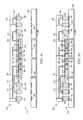
- FIG. 2illustrates a PCB with different types of packages mounted to its surface
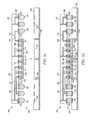
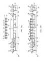
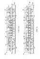
- FIGS. 3 a - 3 cillustrate further detail of the representative semiconductor packages mounted to the PCB
- FIG. 4is a sectional view of an embodiment of a thin high speed chip scale package
- FIG. 5is a sectional view of another embodiment of a thin high speed chip scale package
- FIG. 6is a sectional view of still another embodiment of a thin high speed chip scale package
- FIGS. 7 a - 7 eillustrate a process of dissipating heat from a thin PoP through a TIM to a substrate
- FIGS. 8 a - 8 dillustrate another process of dissipating heat from a thin PoP through a TIM to a substrate
- FIGS. 9 a - 9 dillustrate a heat distributing layer for dissipating heat from a thin semiconductor die mounted to a substrate
- FIGS. 10 a - 10 eillustrate depositing TIM over the semiconductor die or substrate
- FIG. 11illustrates a masking layer to contain underfill material.
- Front-end manufacturinginvolves the formation of a plurality of die on the surface of a semiconductor wafer.
- Each die on the wafercontains active and passive electrical components, which are electrically connected to form functional electrical circuits.
- Active electrical componentssuch as transistors and diodes, have the ability to control the flow of electrical current.
- Passive electrical componentssuch as capacitors, inductors, resistors, and transformers, create a relationship between voltage and current necessary to perform electrical circuit functions.
- Passive and active componentsare formed over the surface of the semiconductor wafer by a series of process steps including doping, deposition, photolithography, etching, and planarization.
- Dopingintroduces impurities into the semiconductor material by techniques such as ion implantation or thermal diffusion.
- the doping processmodifies the electrical conductivity of semiconductor material in active devices, transforming the semiconductor material into an insulator, conductor, or dynamically changing the semiconductor material conductivity in response to an electric field or base current.
- Transistorscontain regions of varying types and degrees of doping arranged as necessary to enable the transistor to promote or restrict the flow of electrical current upon the application of the electric field or base current.
- Active and passive componentsare formed by layers of materials with different electrical properties.
- the layerscan be formed by a variety of deposition techniques determined in part by the type of material being deposited. For example, thin film deposition can involve chemical vapor deposition (CVD), physical vapor deposition (PVD), electrolytic plating, and electroless plating processes.
- CVDchemical vapor deposition
- PVDphysical vapor deposition
- electrolytic platingelectroless plating processes.
- Each layeris generally patterned to form portions of active components, passive components, or electrical connections between components.
- the layerscan be patterned using photolithography, which involves the deposition of light sensitive material, e.g., photoresist, over the layer to be patterned.
- a patternis transferred from a photomask to the photoresist using light.
- the portion of the photoresist pattern subjected to lightis removed using a solvent, exposing portions of the underlying layer to be patterned.
- the portion of the photoresist pattern not subjected to light, the negative photoresistis removed using a solvent, exposing portions of the underlying layer to be patterned.
- the remainder of the photoresistis removed, leaving behind a patterned layer.
- some types of materialsare patterned by directly depositing the material into the areas or voids formed by a previous deposition/etch process using techniques such as electroless and electrolytic plating.
- Planarizationcan be used to remove material from the surface of the wafer and produce a uniformly flat surface. Planarization involves polishing the surface of the wafer with a polishing pad. An abrasive material and corrosive chemical are added to the surface of the wafer during polishing. The combined mechanical action of the abrasive and corrosive action of the chemical removes any irregular topography, resulting in a uniformly flat surface.
- Back-end manufacturingrefers to cutting or singulating the finished wafer into the individual die and then packaging the die for structural support and environmental isolation.
- the waferis scored and broken along non-functional regions of the wafer called saw streets or scribes.
- the waferis singulated using a laser cutting tool or saw blade.
- the individual dieare mounted to a package substrate that includes pins or contact pads for interconnection with other system components.
- Contact pads formed over the semiconductor dieare then connected to contact pads within the package.
- the electrical connectionscan be made with solder bumps, stud bumps, conductive paste, or wirebonds.
- An encapsulant or other molding materialis deposited over the package to provide physical support and electrical isolation.
- the finished packageis then inserted into an electrical system and the functionality of the semiconductor device is made available to the other system components.
- FIG. 2illustrates electronic device 50 having a chip carrier substrate or printed circuit board (PCB) 52 with a plurality of semiconductor packages mounted on its surface.
- Electronic device 50can have one type of semiconductor package, or multiple types of semiconductor packages, depending on the application. The different types of semiconductor packages are shown in FIG. 2 for purposes of illustration.
- Electronic device 50can be a stand-alone system that uses the semiconductor packages to perform one or more electrical functions.
- electronic device 50can be a subcomponent of a larger system.
- electronic device 50can be part of a cellular phone, personal digital assistant (PDA), digital video camera (DVC), or other electronic communication device.
- PDApersonal digital assistant
- DVCdigital video camera
- electronic device 50can be a graphics card, network interface card, or other signal processing card that can be inserted into a computer.
- the semiconductor packagecan include microprocessors, memories, application specific integrated circuits (ASIC), logic circuits, analog circuits, RF circuits, discrete devices, or other semiconductor die or electrical components. Miniaturization and weight reduction are essential for these products to be accepted by the market. The distance between semiconductor devices must be decreased to achieve higher density.
- PCB 52provides a general substrate for structural support and electrical interconnect of the semiconductor packages mounted on the PCB.
- Conductive signal traces 54are formed over a surface or within layers of PCB 52 using evaporation, electrolytic plating, electroless plating, screen printing, or other suitable metal deposition process. Signal traces 54 provide for electrical communication between each of the semiconductor packages, mounted components, and other external system components. Traces 54 also provide power and ground connections to each of the semiconductor packages.
- a semiconductor devicehas two packaging levels.
- First level packagingis a technique for mechanically and electrically attaching the semiconductor die to an intermediate carrier.
- Second level packaginginvolves mechanically and electrically attaching the intermediate carrier to the PCB.
- a semiconductor devicemay only have the first level packaging where the die is mechanically and electrically mounted directly to the PCB.
- first level packagingincluding bond wire package 56 and flip chip 58
- second level packagingincluding ball grid array (BGA) 60 , bump chip carrier (BCC) 62 , dual in-line package (DIP) 64 , land grid array (LGA) 66 , multi-chip module (MCM) 68 , quad flat non-leaded package (QFN) 70 , and quad flat package 72 .
- BGAball grid array
- BCCbump chip carrier
- DIPdual in-line package
- LGAland grid array
- MCMmulti-chip module
- QFNquad flat non-leaded package
- quad flat package 72quad flat package
- electronic device 50includes a single attached semiconductor package, while other embodiments call for multiple interconnected packages.
- manufacturerscan incorporate pre-made components into electronic devices and systems. Because the semiconductor packages include sophisticated functionality, electronic devices can be manufactured using cheaper components and a streamlined manufacturing process. The resulting devices are less likely to fail and less expensive to manufacture resulting in a lower cost for consumers.
- FIGS. 3 a - 3 cshow exemplary semiconductor packages.
- FIG. 3 aillustrates further detail of DIP 64 mounted on PCB 52 .
- Semiconductor die 74includes an active region containing analog or digital circuits implemented as active devices, passive devices, conductive layers, and dielectric layers formed within the die and are electrically interconnected according to the electrical design of the die.
- the circuitcan include one or more transistors, diodes, inductors, capacitors, resistors, and other circuit elements formed within the active region of semiconductor die 74 .
- Contact pads 76are one or more layers of conductive material, such as aluminum (Al), copper (Cu), tin (Sn), nickel (Ni), gold (Au), or silver (Ag), and are electrically connected to the circuit elements formed within semiconductor die 74 .
- semiconductor die 74is mounted to an intermediate carrier 78 using a gold-silicon eutectic layer or adhesive material such as thermal epoxy or epoxy resin.
- the package bodyincludes an insulative packaging material such as polymer or ceramic.
- Conductor leads 80 and bond wires 82provide electrical interconnect between semiconductor die 74 and PCB 52 .
- Encapsulant 84is deposited over the package for environmental protection by preventing moisture and particles from entering the package and contaminating die 74 or bond wires 82 .
- FIG. 3 billustrates further detail of BCC 62 mounted on PCB 52 .
- Semiconductor die 88is mounted over carrier 90 using an underfill or epoxy-resin adhesive material 92 .
- Bond wires 94provide first level packaging interconnect between contact pads 96 and 98 .
- Molding compound or encapsulant 100is deposited over semiconductor die 88 and bond wires 94 to provide physical support and electrical isolation for the device.
- Contact pads 102are formed over a surface of PCB 52 using a suitable metal deposition process such as electrolytic plating or electroless plating to prevent oxidation.
- Contact pads 102are electrically connected to one or more conductive signal traces 54 in PCB 52 .
- Bumps 104are formed between contact pads 98 of BCC 62 and contact pads 102 of PCB 52 .
- semiconductor die 58is mounted face down to intermediate carrier 106 with a flip chip style first level packaging.
- Active region 108 of semiconductor die 58contains analog or digital circuits implemented as active devices, passive devices, conductive layers, and dielectric layers formed according to the electrical design of the die.
- the circuitcan include one or more transistors, diodes, inductors, capacitors, resistors, and other circuit elements within active region 108 .
- Semiconductor die 58is electrically and mechanically connected to carrier 106 through bumps 110 .
- BGA 60is electrically and mechanically connected to PCB 52 with a BGA style second level packaging using bumps 112 .
- Semiconductor die 58is electrically connected to conductive signal traces 54 in PCB 52 through bumps 110 , signal lines 114 , and bumps 112 .
- a molding compound or encapsulant 116is deposited over semiconductor die 58 and carrier 106 to provide physical support and electrical isolation for the device.
- the flip chip semiconductor deviceprovides a short electrical conduction path from the active devices on semiconductor die 58 to conduction tracks on PCB 52 in order to reduce signal propagation distance, lower capacitance, and improve overall circuit performance.
- the semiconductor die 58can be mechanically and electrically connected directly to PCB 52 using flip chip style first level packaging without intermediate carrier 106 .
- FIG. 4illustrates a chip scale package 120 having substrate 122 and flipchip semiconductor die 124 mounted to surface 126 of the substrate using bumps 128 .
- the electrical interconnection between semiconductor die 124 and substrate 122is made by way of bumps 128 and a plurality of conductive traces formed on active surface 130 .
- Bumps 128are formed on contact pads on active surface 130 and electrically connected to interconnect sites 131 on substrate 122 in a solid-state fashion, that is, the bumps are thermo-mechanically connected to interconnect sites 131 by concurrently forcing the bumps against the interconnect sites and applying sufficient heat to deform the bump against the interconnect site without melting either the bump material or interconnect site material.
- the solid-state interconnectcan provide for interconnect geometries in ranges less than 0.1 mm pitch.
- the solid-state bondsprovide finer interconnect geometries with a high input/output (I/O) count than can be obtained using a melt-bond connection.
- Bumps 128can also be reflowed to metallurgically and electrically connect to interconnect sites 131 .
- a plurality of bumps 132is formed over contact pads 133 on surface 126 .
- semiconductor die 124is located in a center region of substrate 122 and bumps 132 are arranged around a peripheral region of semiconductor die 124 to the edge of the substrate.
- An underfill material or epoxy-resin adhesive material 134is deposited in the thin gap between substrate 122 and semiconductor die 124 .
- the gap between substrate 122 and active surface 130is less than about 0.025 mm.
- Substrate 122includes a plurality of conductive traces formed on surface 126 to electrically connect bumps 128 and 132 .
- One or more of the conductive traces on substrate 122can be formed as coplanar waveguides, in which ground lines are formed to run alongside the signal line on a planar dielectric material.
- Chip scale package 120achieves miniaturization and high-speed operation by employing a flipchip interconnection between substrate 122 and semiconductor die 124 , and further by mounting the semiconductor die on the same side of the substrate as bumps 132 , which provide a second level interconnect.
- the thickness of substrate 122can be 0.1 mm
- the height of semiconductor die 124can be 0.18 mm
- the height of bumps 132can be 0.3 mm with a 0.5 mm pitch, to yield an overall package height of approximately 0.4 mm.
- the combined thickness of semiconductor die 124 and the gapis less than or equal to the height of bumps 132 so that the effective die thickness is accommodated within the second level interconnect, and contributes nothing to the overall package thickness (“Z” direction miniaturization).
- the second level interconnect reliabilityis superior to that of conventional chip scale packages having bumps within the footprint of the die.
- the length of the longest conductive trace between bumps 128 and bumps 132is less that 1.0 mm, which provides enhanced electrical performance.
- Ground plane 136is formed over surface 138 of substrate 122 , opposite surface 126 .
- Ground plane 136can be a continuous metal sheet, e.g., Cu, substantially covering surface 138 .
- One or more conductive vias 140are formed through substrate 122 to electrically connect ground plane 136 through bumps 132 to a low-impedance ground point.
- FIG. 5shows an embodiment, continuing from FIG. 4 , with a semiconductor die 150 mounted to surface 138 of substrate 122 with a die attach adhesive.
- Semiconductor die 150has contact pads 152 electrically connected to conductive traces 153 formed on surface 138 and conductive vias 140 with bond wires 154 .
- Semiconductor die 150is thus electrically connected to semiconductor die 124 and bumps 132 .
- An encapsulant 156is deposited over surface 138 , semiconductor die 150 , and bond wires 154 .
- FIG. 6shows an embodiment, continuing from FIG. 4 , with a flipchip semiconductor die 160 mounted to surface 138 of substrate 122 using bump 162 .
- Bumps 162are electrically connected to conductive traces or redistribution layer (RDL) 163 formed on surface 138 and conductive vias 140 .
- Semiconductor die 160is thus electrically connected to semiconductor die 124 and bumps 132 .
- An underfill material or epoxy-resin adhesive material 164is deposited between substrate 122 and semiconductor die 160 .
- FIGS. 7 a - 7 eillustrate, in relation to FIGS. 2 and 3 a - 3 c , a process of dissipating heat from a thin PoP mounted to a substrate.
- FIG. 7 ashows a substrate 170 having electrically conductive layers or traces 172 formed over and through the substrate to provide electrical interconnect according to the electrical design and function of semiconductor die 190 and 200 .
- the conductive layers and traces 172extend across surface 174 of substrate 170 and through the substrate between opposing surfaces 174 and 176 with electrical separation by insulating material 178 .
- a plurality of bumps 180is formed over contact pads 182 on surface 174 and electrically connected to conductive traces 172 .
- a semiconductor die 190has an active surface 192 containing analog or digital circuits implemented as active devices, passive devices, conductive layers, and dielectric layers formed within the die and electrically interconnected according to the electrical design and function of the die.
- the circuitcan include one or more transistors, diodes, and other circuit elements formed within active surface 192 to implement analog circuits or digital circuits, such as digital signal processor (DSP), central processing unit (CPU), ASIC, memory, or other signal processing circuit.
- DSPdigital signal processor
- CPUcentral processing unit
- ASICapplication specific integrated circuit
- Semiconductor die 190can also contain IPDs, such as inductors, capacitors, and resistors, for RF signal processing.
- a plurality of bumps 194is formed over contact pads 195 on active surface 192 for electrical interconnect.
- a semiconductor die 200has an active surface 202 containing analog or digital circuits implemented as active devices, passive devices, conductive layers, and dielectric layers formed within the die and electrically interconnected according to the electrical design and function of the die.
- the circuitcan include one or more transistors, diodes, and other circuit elements formed within active surface 202 to implement analog circuits or digital circuits, such as DSP, CPU, ASIC, memory, or other signal processing circuit.
- Semiconductor die 200can also contain IPDs, such as inductors, capacitors, and resistors, for RF signal processing.
- a plurality of bumps 204is formed over contact pads 205 on active surface 202 , outside a footprint of semiconductor die 190 , for electrical interconnect.
- Semiconductor die 200is mounted to semiconductor die 190 .
- Semiconductor die 190 and 200are mounted to a central region 206 of surface 174 , as shown in FIG. 7 b .
- Bumps 194are electrically connected to contact pads 208 and conductive traces 172 on substrate 170 using reflow or solid-state bonding.
- bumps 204are electrically connected to contact pads 210 and conductive traces 172 on substrate 170 using reflow or solid-state bonding. In solid-state bonding, bumps 194 and 204 are thermo-mechanically connected to the contact pads by concurrently forcing the bumps against the contact pads and applying sufficient heat to deform the bumps against the pads without melting either the bump material or pad material.
- An underfill material or epoxy-resin adhesive material 212is deposited between substrate 170 and semiconductor die 190 and 200 .
- Semiconductor die 190has a smaller footprint as compared to semiconductor die 200 so that bumps 204 can be electrically connected to contact pads 210 around a peripheral region of semiconductor die 190 .
- Semiconductor die 190 and 200constitute an ultra thin package-on-package (PoP) arrangement mounted to substrate 170 between bumps 180 .
- the combined height of semiconductor die 190 and 200 with bumps 194 and 204is less than or equal to the height of bumps 180 .
- FIG. 7 cshows substrate or PCB 224 with thermal conduction channels 226 routed through the PCB to conductive plane 225 .
- the PoP and substrate structure 214is inverted and positioned over thermal conduction channels 226 .
- a thermal interface material (TIM) 220is deposited over back surface 222 of semiconductor die 200 , opposite semiconductor die 190 .
- TIM 220can be applied to thermal conduction channel 226 of PCB 224 .
- the PoP and substrate structure 214is mounted to thermal conduction channels 226 of PCB 224 with TIM 220 , as shown in FIG. 7 d .
- Bumps 180are electrically connected to contact pads 227 on PCB 224 .
- semiconductor die 200is a DSP, CPU, or other heat-generating signal processing die
- semiconductor die 190is a memory supporting the DSP or CPU.
- semiconductor die 190is the DSP, CPU, or other heat-generating signal processing die
- semiconductor die 200is the memory supporting the DSP or CPU.
- semiconductor die 190 and 200can operate with, for example, up to 5 watts of power consumption.
- Semiconductor die 190 and 200are electrically connected through bumps 194 and 204 , and conductive layers or traces 172 to PCB 224 .
- the heat generated by semiconductor die 190 and 200is dissipated through TIM 220 and thermal conduction channels 226 to conductive plane 225 .
- Conductive plane 225can be securely mounted to equipment or chassis for further heat distribution.
- Conductive plane 225can also serve as a ground plane for semiconductor die 190 and 200 to the equipment, as well as heat distribution.
- the PoP and substrate structure 214can handle high power devices and provide effective heat dissipation with a high I/O count, all in an ultra thin PoP package.
- ground plane 228is formed over surface 176 of substrate 170 .
- Ground plane 228can be a continuous metal sheet, e.g., Cu, substantially covering surface 176 .
- Ground plane 228is electrically connected through conductive traces 172 and bumps 180 to a low-impedance ground point.
- a semiconductor diecan be mounted to surface 176 , as shown in FIGS. 5 and 6 .
- FIGS. 8 a - 8 dillustrate, in relation to FIGS. 2 and 3 a - 3 c , another process of dissipating heat from a thin PoP mounted to a substrate.
- FIG. 8 ashows a substrate 230 having electrically conductive layers or traces 232 formed over and through the substrate to provide electrical interconnect according to the electrical design and function of semiconductor die 250 and 260 .
- the conductive layers and traces 232extend across substrate 230 and through the substrate between surface 234 and opposing surface 236 with electrical separation by insulating layer 238 .
- a plurality of bumps 240is formed over contact pads 242 on surface 234 of substrate 230 and electrically connected to conductive traces 232 .
- a semiconductor die 250has an active surface 252 containing analog or digital circuits implemented as active devices, passive devices, conductive layers, and dielectric layers formed within the die and electrically interconnected according to the electrical design and function of the die.
- the circuitcan include one or more transistors, diodes, and other circuit elements formed within active surface 252 to implement analog circuits or digital circuits, such as DSP, CPU, ASIC, memory, or other signal processing circuit.
- Semiconductor die 250can also contain IPDs, such as inductors, capacitors, and resistors, for RF signal processing.
- a plurality of bumps 254is formed over contact pads 256 on active surface 252 for electrical interconnect.
- a plurality of viasis formed through semiconductor die 250 using mechanical drilling, laser drilling, or deep reactive ion etching (DRIE).
- the viasare filled with Al, Cu, Sn, Ni, Au, Ag, titanium (Ti), tungsten (W), polysilicon, or other suitable electrically conductive material using electrolytic plating, electroless plating process, or other suitable metal deposition process to form z-direction conductive through silicon vias (TSV) 258 .
- a semiconductor die 260has an active surface 262 containing analog or digital circuits implemented as active devices, passive devices, conductive layers, and dielectric layers formed within the die and electrically interconnected according to the electrical design and function of the die.
- the circuitcan include one or more transistors, diodes, and other circuit elements formed within active surface 262 to implement analog circuits or digital circuits, such as DSP, CPU, ASIC, memory, or other signal processing circuit.
- Semiconductor die 260can also contain IPDs, such as inductors, capacitors, and resistors, for RF signal processing.
- a plurality of bumps 264is formed over contact pads 265 on active surface 262 for electrical interconnect.
- Semiconductor die 250is mounted to a central region 266 of surface 234 , as shown in FIG. 8 b .
- Bumps 254are electrically connected to contact pads 268 and conductive traces 232 on substrate 230 using reflow or solid-state bonding.
- Semiconductor die 260is mounted to semiconductor die 250 with bumps 264 electrically connected to conductive TSV 258 using reflow or solid-state bonding.
- Semiconductor die 260is further electrically connected through conductive TSV 258 and bumps 254 to contact pads 268 and conductive traces 232 on substrate 230 .
- bumps 254 and 264are thermo-mechanically connected to the contact pads by concurrently forcing the bumps against the contact pads and applying sufficient heat to deform the bumps against the pads without melting either the bump material or pad material.
- Semiconductor die 260has a substantially similar footprint as semiconductor die 250 .
- An underfill material or epoxy-resin adhesive material 270is deposited between substrate 230 and semiconductor die 250 and 260 .
- Semiconductor die 250 and 260constitute an ultra thin PoP arrangement mounted to substrate 230 between bumps 240 .
- the combined height of semiconductor die 250 and 260 with bumps 254 and 264is less than or equal to the height of bumps 240 .
- FIG. 8 cshows substrate or PCB 280 with thermal conduction channels 282 routed through the PCB to conductive plane 285 .
- the PoP and substrate structure 274is inverted and TIM 276 is deposited over back surface 278 of semiconductor die 260 , opposite semiconductor die 250 .
- TIM 276can be applied to thermal conduction channel 282 of PCB 224 .
- the PoP and substrate structure 274is mounted to thermal conduction channels 282 of PCB 280 with TIM 276 , as shown in FIG. 8 d .
- Bumps 240are electrically connected to contact pads 284 on PCB 280 .
- semiconductor die 260is a DSP, CPU, or other heat-generating signal processing die
- semiconductor die 250is a memory supporting the DSP or CPU.
- semiconductor die 250is the DSP, CPU, or other heat-generating signal processing die
- semiconductor die 260is the memory supporting the DSP or CPU. In either case, semiconductor die 250 and 260 can operate with, for example, up to 5 watts of power consumption.
- Semiconductor die 250 and 260are electrically connected through conductive TSV 258 , bumps 264 , 254 , and 240 , and conductive layers or traces 232 to PCB 280 .
- the heat generated by semiconductor die 250 and 260is dissipated through TIM 276 and thermal conduction channels 282 to conductive plane 285 for heat dissipation.
- Conductive plane 285can be securely mounted to equipment or chassis for further heat distribution.
- Conductive plane 285can also serve as a ground plane for semiconductor die 250 and 260 to the equipment, as well as heat distribution.
- the PoP and substrate structure 274can handle high power devices and provide effective heat dissipation with a high I/O count, all in an ultra thin PoP package.
- FIG. 9 ashows a substrate 290 having electrically conductive layers or traces 292 formed over and through the substrate to provide electrical interconnect according to the electrical design and function of semiconductor die 310 .
- the conductive layers and traces 292extend across substrate 290 and through the substrate between surface 294 and opposing surface 296 with electrical separation by insulating layer 298 .
- a plurality of bumps 300is formed over contact pads 302 on surface 294 of substrate 290 and electrically connected to conductive traces 292 .
- a semiconductor die 310has an active surface 312 containing analog or digital circuits implemented as active devices, passive devices, conductive layers, and dielectric layers formed within the die and electrically interconnected according to the electrical design and function of the die.
- the circuitcan include one or more transistors, diodes, and other circuit elements formed within active surface 312 to implement analog circuits or digital circuits, such as DSP, CPU, ASIC, memory, or other signal processing circuit.
- Semiconductor die 310can also contain IPDs, such as inductors, capacitors, and resistors, for RF signal processing.
- a plurality of bumps 314is formed over contact pads 315 on active surface 312 for electrical interconnect.
- a second semiconductor diecan be mounted to semiconductor die 310 , similar to FIG. 8 a.
- a TIM 316is formed over back surface 318 of semiconductor die 310 to aid with distribution and dissipation of heat generated by the semiconductor die.
- TIM 316can be aluminum oxide, zinc oxide, boron nitride, or pulverized silver.
- An optional heat distributing layer 320is mounted over TIM 316 .
- Heat distributing layer 320can be Cu, Al, or other material with high thermal conductivity.
- Semiconductor die 310 with heat distributing layer 320is mounted to a central region 322 of surface 294 , as shown in FIG. 9 b .
- Bumps 314are electrically connected to contact pads 324 and conductive traces 292 on substrate 290 using reflow or solid-state bonding. In solid-state bonding, bumps 314 are thermo-mechanically connected to the contact pads by concurrently forcing the bumps against the contact pads and applying sufficient heat to deform the bumps against the pads without melting either the bump material or pad material.
- An underfill material or epoxy-resin adhesive material 326is deposited between substrate 290 and semiconductor die 310 .
- the combined height of semiconductor die 310 with bumps 314 , TIM 316 , and heat distributing layer 320is less than or equal to the height of bumps 300 .
- FIG. 9 cshows substrate or PCB 330 with thermal conduction channels 332 routed through the PCB to conductive plane 336 .
- the semiconductor die and substrate structure 328is inverted and mounted to PCB 330 with heat distributing layer 320 contacting thermal conduction channels 332 .
- Bumps 300are electrically connected to contact pads 334 on PCB 330 , as shown in FIG. 9 d .
- semiconductor die 310is a DSP, CPU, or other heat-generating signal processing die. In this case, semiconductor die 310 can operate with, for example, up to 5 watts of power consumption.
- Semiconductor die 310is electrically connected through bumps 314 and 300 to conductive layers or traces 292 of PCB 330 .
- the heat generated by semiconductor die 310is dissipated through TIM 316 , heat distributing layer 320 , and thermal conduction channels 332 to conductive plane 336 of PCB 330 .
- the semiconductor die and substrate structure 328can handle high power devices and provide effective heat dissipation with a high I/O count, all in an ultra thin PoP package.
- FIG. 10 a - 10 eshows an embodiment with a substrate 340 having electrically conductive layers or traces 342 formed over and through the substrate to provide electrical interconnect according to the electrical design and function of semiconductor die 360 and 370 .
- the conductive layers and traces 342extend across substrate 340 and through the substrate between surface 344 and opposing surface 346 with electrical separation by insulating layer 348 .
- a plurality of bumps 350is formed over contact pads 352 on surface 344 of substrate 340 and electrically connected to conductive traces 342 .
- a semiconductor die 360has an active surface 362 containing analog or digital circuits implemented as active devices, passive devices, conductive layers, and dielectric layers formed within the die and electrically interconnected according to the electrical design and function of the die.
- the circuitcan include one or more transistors, diodes, and other circuit elements formed within active surface 362 to implement analog circuits or digital circuits, such as DSP, CPU, ASIC, memory, or other signal processing circuit.
- Semiconductor die 360can also contain IPDs, such as inductors, capacitors, and resistors, for RF signal processing.
- a plurality of bumps 364is formed over contact pads 366 on active surface 362 for electrical interconnect.
- a plurality of viasis formed through semiconductor die 360 using mechanical drilling, laser drilling, or DRIE.
- the viasare filled with Al, Cu, Sn, Ni, Au, Ag, Ti, W, polysilicon, or other suitable electrically conductive material using electrolytic plating, electroless plating process, or other suitable metal deposition process to form z-direction conductive TSV 368 .
- a semiconductor die 370has an active surface 372 containing analog or digital circuits implemented as active devices, passive devices, conductive layers, and dielectric layers formed within the die and electrically interconnected according to the electrical design and function of the die.
- the circuitcan include one or more transistors, diodes, and other circuit elements formed within active surface 372 to implement analog circuits or digital circuits, such as DSP, CPU, ASIC, memory, or other signal processing circuit.
- Semiconductor die 370can also contain IPDs, such as inductors, capacitors, and resistors, for RF signal processing.
- a plurality of contact pads 374is formed on active surface 372 .
- Semiconductor die 370is mounted to the back surface of semiconductor die 360 and electrically connected through conductive TSV 368 to bumps 364 .
- Semiconductor die 360 and 370can be similar size or different size, similar to FIGS. 7 a and 8 a.
- Bumps 364are electrically connected to contact pads 378 and conductive traces 342 on substrate 340 using reflow or solid-state bonding. In solid-state bonding, bumps 364 are thermo-mechanically connected to the contact pads by concurrently forcing the bumps against the contact pads and applying sufficient heat to deform the bumps against the pads without melting either the bump material or pad material.
- An underfill material or epoxy-resin adhesive material 380is deposited between substrate 340 and semiconductor die 360 and 370 .
- semiconductor die 370is a DSP, CPU, or other heat-generating signal processing die
- semiconductor die 360is a memory supporting the DSP or CPU.
- semiconductor die 360is the DSP, CPU, or other heat-generating signal processing die
- semiconductor die 370is the memory supporting the DSP or CPU.
- semiconductor die 360 or 370can operate with, for example, up to 5 watts of power consumption.
- the combined height of semiconductor die 360 with bumps 364 and semiconductor die 370is less than or equal to the height of bumps 350 .
- FIG. 10 cshows substrate or PCB 384 with contact pads 386 connected to signal trace lines routed over surface 388 and within the layers of the PCB.
- Thermal conduction channels 390are routed through PCB 384 to conductive plane 392 formed over surface 394 of the PCB opposite surface 388 .
- a TIM 396is deposited over surface 388 of PCB 340 in the area designated for mounting semiconductor die 360 and 370 to aid with distribution and dissipation of heat generated by the semiconductor die.
- TIM 396can be aluminum oxide, zinc oxide, boron nitride, or pulverized silver.
- TIM 396can be solder paste, heat-conductive polymer material, b-stage adhesive, thermal pad, or other thermal coupling agent.
- FIG. 10 dshows an embodiment with TIM 396 deposited over the back surface of semiconductor die 370 .
- the semiconductor die and substrate structure 398is inverted and mounted to substrate or PCB 340 .
- the back surface of semiconductor die 370opposite active surface 372 , is thermally bonded to surface 388 of PCB 340 with TIM 396 , as shown in FIG. 10 e .
- TIM 396can be reflowed to molten state and then solidified to thermally bond the back surface of semiconductor die 370 to surface 388 of PCB 340 .
- the materialcan be cured to thermally bond the back surface of semiconductor die 370 to surface 388 of PCB 340 .
- Bumps 350are electrically connected to contact pads 386 .
- Semiconductor die 360 and 370are electrically connected through conductive TSV 368 and bumps 364 and 350 to conductive layers or traces 342 of PCB 340 .
- the heat generated by semiconductor die 360 and 370is dissipated through TIM 396 and thermal conduction channels 390 to conductive plane 392 of PCB 340 .
- Conductive plane 392can be securely mounted to equipment or chassis for further heat distribution. Alternatively, a heat sink can be mounted to conductive plane 392 .
- Conductive plane 392can also serve as a ground plane for semiconductor die 360 and 370 to the equipment, as well as heat distribution.
- the semiconductor die and substrate structure 398can handle high power devices and provide effective heat dissipation with a high I/O count, all in an ultra thin PoP package.
- FIG. 11shows an embodiment, similar to FIG. 10 e , with solder resist or masking layer 400 .
- Masking layer 400includes bump openings for bumps 350 and bumps 364 in an interior region of semiconductor die 360 . The portion of masking layer 400 around bumps 364 around a perimeter of semiconductor die 364 is open. Masking layer 400 acts as resin dam to contain underfill material 380 .
Landscapes
- Engineering & Computer Science (AREA)
- Microelectronics & Electronic Packaging (AREA)
- Power Engineering (AREA)
- Computer Hardware Design (AREA)
- Physics & Mathematics (AREA)
- Condensed Matter Physics & Semiconductors (AREA)
- General Physics & Mathematics (AREA)
- Manufacturing & Machinery (AREA)
- Cooling Or The Like Of Semiconductors Or Solid State Devices (AREA)
- Semiconductor Integrated Circuits (AREA)
Abstract
Description
- The present application is a continuation-in-part of U.S. application Ser. No. 10/960,893, filed Oct. 7, 2004, and claims priority to the foregoing application pursuant to 35 U.S.C. §120.
- Semiconductor devices are commonly found in modern electronic products. Semiconductor devices vary in the number and density of electrical components. Discrete semiconductor devices generally contain one type of electrical component, e.g., light emitting diode (LED), small signal transistor, resistor, capacitor, inductor, and power metal oxide semiconductor field effect transistor (MOSFET). Integrated semiconductor devices typically contain hundreds to millions of electrical components. Examples of integrated semiconductor devices include microcontrollers, microprocessors, charged-coupled devices (CCDs), solar cells, and digital micro-mirror devices (DMDs).
- Semiconductor devices perform a wide range of functions such as signal processing, high-speed calculations, transmitting and receiving electromagnetic signals, controlling electronic devices, transforming sunlight to electricity, and creating visual projections for television displays. Semiconductor devices are found in the fields of entertainment, communications, power conversion, networks, computers, and consumer products. Semiconductor devices are also found in military applications, aviation, automotive, industrial controllers, and office equipment.
- Semiconductor devices exploit the electrical properties of semiconductor materials. The atomic structure of semiconductor material allows its electrical conductivity to be manipulated by the application of an electric field or base current or through the process of doping. Doping introduces impurities into the semiconductor material to manipulate and control the conductivity of the semiconductor device.
- A semiconductor device contains active and passive electrical structures. Active structures, including bipolar and field effect transistors, control the flow of electrical current. By varying levels of doping and application of an electric field or base current, the transistor either promotes or restricts the flow of electrical current. Passive structures, including resistors, capacitors, and inductors, create a relationship between voltage and current necessary to perform a variety of electrical functions. The passive and active structures are electrically connected to form circuits, which enable the semiconductor device to perform high-speed calculations and other useful functions.
- Semiconductor devices are generally manufactured using two complex manufacturing processes, i.e., front-end manufacturing, and back-end manufacturing, each involving potentially hundreds of steps. Front-end manufacturing involves the formation of a plurality of die on the surface of a semiconductor wafer. Each die is typically identical and contains circuits formed by electrically connecting active and passive components. Back-end manufacturing involves singulating individual die from the finished wafer and packaging the die to provide structural support and environmental isolation.
- One goal of semiconductor manufacturing is to produce smaller semiconductor devices. Smaller devices typically consume less power, have higher performance, and can be produced more efficiently. In addition, smaller semiconductor devices have a smaller footprint, which is desirable for smaller end products. A smaller die size can be achieved by improvements in the front-end process resulting in die with smaller, higher density active and passive components. Back-end processes may result in semiconductor device packages with a smaller footprint by improvements in electrical interconnection and packaging materials.
- Another goal of semiconductor manufacturing is to produce semiconductor devices with adequate heat dissipation. High frequency and high power consumption semiconductor devices generally generate more heat. Without effective heat dissipation, the generated heat can reduce performance, decrease reliability, and reduce the useful lifetime of the semiconductor device.
- Chip scale packages housing semiconductor die are in increasing demand in applications such as hand-held or portable electronics and in miniaturized storage devices, such as disk drives. In many such applications, there is a need for such packages to operate at very high frequencies, typically in excess of 1 GHz, to meet the needs of analog or RF devices and of fast memories used in cellular phones. Chip scale packages are in common use in such applications. Chip scale packages conventionally employ wire bonding to electrically connect the semiconductor die and substrate.
FIG. 1 shows a conventionalchip scale package 10 withsemiconductor die 14 attached tosurface 11 ofsubstrate 12. Semiconductor die14 is electrically connected tosubstrate 12 by way ofbond wires 16 connected betweenbond wire pads 15 on semiconductor die14 andinterconnect sites 18 onsurface 11. Semiconductor die14,bond wires 16, andsurface 11 ofsubstrate 12 are enclosed within and protected byencapsulant 20. A plurality of secondlevel interconnect bumps 22 is attached tointerconnect sites 24 onsurface 26 ofsubstrate 12,opposite surface 11.Substrate 12 includes electrically conductive traces formed at or nearsurface 11 andsurface 26 for connection withbond wires 16 fromsemiconductor die 14 andbumps 22. A plurality of vias can be formed throughsubstrate 12 to electrically interconnect features onsurfaces - It is desirable to minimize thickness of the chip scale package. Chip scale packages with bond wire interconnect have an overall package height in the range of 0.6-0.8 millimeters (mm). Further reduction of package thickness is increasingly difficult in part due to the fact that wire bonding interconnection employs wire loops of finite height imposing lower limits on size in the “Z” direction) and finite span imposing lower limits on size in the “X” and “Y” directions. The bond wires are routed from bond pads at the upper surface of the die, up and then across and down to bond sites on the upper surface of the substrate onto which the die is attached. The bond wires are enclosed with a protective encapsulating material. The bond wires and encapsulation typically contribute about 0.2-0.4 mm to the package thickness. In addition, as chip scale packages are made thinner, the second level interconnections between the package and the printed circuit board are less reliable. In particular, second level interconnections that lie under the footprint of the semiconductor die are most adversely affected.
- Moreover, improvement of electrical performance presents significant challenges because of the difficulty in reducing the signal path length, as the bond wires typically have a length about 1.0 mm. The structure of the package necessitates wrap-around routing of conductive traces as the traces fan outward to vias and run back inward to the bump locations.
- A need exists for a package structure that circumvents the above obstacles and provides for further package miniaturization, improved high-speed operation, and effective power dissipation. Accordingly, in one embodiment, the present invention is a method of making a semiconductor device comprising the steps of providing a first substrate having a central region, forming a plurality of bumps around a periphery of the central region of the first substrate, mounting a first semiconductor die to the central region of the first substrate, and mounting a second semiconductor die to the first semiconductor die over the central region of the first substrate. A height of the first and second semiconductor die is less than or equal to a height of the bumps. The method further includes the steps of providing a second substrate having a thermal conduction channel, mounting a surface of the second semiconductor die opposite the first semiconductor die to the thermal conductive channel of the second substrate with a thermal interface material, and electrically connecting the bumps to contact pads on the second substrate.
- In another embodiment, the present invention is a method of making a semiconductor device comprising the steps of providing a first substrate, mounting a first semiconductor die to the first substrate, mounting a second semiconductor die to the first semiconductor die over the first substrate, and forming a plurality of bumps over the first substrate around a periphery of the first and second semiconductor die. A height of the first and second semiconductor die is less than or equal to a height of the bumps. The method further includes the steps of providing a second substrate having a thermal conduction channel, and mounting a surface of the second semiconductor die opposite the first semiconductor die to the thermal conductive channel of the second substrate with a thermal interface material.
- In another embodiment, the present invention is a method of making a semiconductor device comprising the steps of providing a first substrate, mounting a first semiconductor die to the first substrate, and forming a plurality of bumps over the first substrate around a periphery of the first semiconductor die. A height of the first semiconductor die is less than or equal to a height of the bumps. The method further includes the steps of providing a second substrate having a thermal conduction channel, and mounting a surface of the first semiconductor die to the thermal conductive channel of the second substrate with a thermal interface material.
- In another embodiment, the present invention is a semiconductor device comprising a first substrate and first semiconductor die mounted to the first substrate. A second semiconductor die is mounted to the first semiconductor die over the first substrate. A plurality of bumps is formed over the first substrate around a periphery of the first and second semiconductor die. A height of the first and second semiconductor die is less than or equal to a height of the bumps. A second substrate has a thermal conduction channel. A surface of the second semiconductor die opposite the first semiconductor die is mounted to the thermal conductive channel of the second substrate with a thermal interface material.
FIG. 1 is a sectional view of a conventional chip scale package having bond wire interconnection;FIG. 2 illustrates a PCB with different types of packages mounted to its surface;FIGS. 3 a-3cillustrate further detail of the representative semiconductor packages mounted to the PCB;FIG. 4 is a sectional view of an embodiment of a thin high speed chip scale package;FIG. 5 is a sectional view of another embodiment of a thin high speed chip scale package;FIG. 6 is a sectional view of still another embodiment of a thin high speed chip scale package;FIGS. 7 a-7eillustrate a process of dissipating heat from a thin PoP through a TIM to a substrate;FIGS. 8 a-8dillustrate another process of dissipating heat from a thin PoP through a TIM to a substrate;FIGS. 9 a-9dillustrate a heat distributing layer for dissipating heat from a thin semiconductor die mounted to a substrate;FIGS. 10 a-10eillustrate depositing TIM over the semiconductor die or substrate; andFIG. 11 illustrates a masking layer to contain underfill material.- The present invention is described in one or more embodiments in the following description with reference to the figures, in which like numerals represent the same or similar elements. While the invention is described in terms of the best mode for achieving the invention's objectives, it will be appreciated by those skilled in the art that it is intended to cover alternatives, modifications, and equivalents as may be included within the spirit and scope of the invention as defined by the appended claims and their equivalents as supported by the following disclosure and drawings.
- Semiconductor devices are generally manufactured using two complex manufacturing processes: front-end manufacturing and back-end manufacturing. Front-end manufacturing involves the formation of a plurality of die on the surface of a semiconductor wafer. Each die on the wafer contains active and passive electrical components, which are electrically connected to form functional electrical circuits. Active electrical components, such as transistors and diodes, have the ability to control the flow of electrical current. Passive electrical components, such as capacitors, inductors, resistors, and transformers, create a relationship between voltage and current necessary to perform electrical circuit functions.
- Passive and active components are formed over the surface of the semiconductor wafer by a series of process steps including doping, deposition, photolithography, etching, and planarization. Doping introduces impurities into the semiconductor material by techniques such as ion implantation or thermal diffusion. The doping process modifies the electrical conductivity of semiconductor material in active devices, transforming the semiconductor material into an insulator, conductor, or dynamically changing the semiconductor material conductivity in response to an electric field or base current. Transistors contain regions of varying types and degrees of doping arranged as necessary to enable the transistor to promote or restrict the flow of electrical current upon the application of the electric field or base current.
- Active and passive components are formed by layers of materials with different electrical properties. The layers can be formed by a variety of deposition techniques determined in part by the type of material being deposited. For example, thin film deposition can involve chemical vapor deposition (CVD), physical vapor deposition (PVD), electrolytic plating, and electroless plating processes. Each layer is generally patterned to form portions of active components, passive components, or electrical connections between components.
- The layers can be patterned using photolithography, which involves the deposition of light sensitive material, e.g., photoresist, over the layer to be patterned. A pattern is transferred from a photomask to the photoresist using light. In one embodiment, the portion of the photoresist pattern subjected to light is removed using a solvent, exposing portions of the underlying layer to be patterned. In another embodiment, the portion of the photoresist pattern not subjected to light, the negative photoresist, is removed using a solvent, exposing portions of the underlying layer to be patterned. The remainder of the photoresist is removed, leaving behind a patterned layer. Alternatively, some types of materials are patterned by directly depositing the material into the areas or voids formed by a previous deposition/etch process using techniques such as electroless and electrolytic plating.
- Depositing a thin film of material over an existing pattern can exaggerate the underlying pattern and create a non-uniformly flat surface. A uniformly flat surface is required to produce smaller and more densely packed active and passive components. Planarization can be used to remove material from the surface of the wafer and produce a uniformly flat surface. Planarization involves polishing the surface of the wafer with a polishing pad. An abrasive material and corrosive chemical are added to the surface of the wafer during polishing. The combined mechanical action of the abrasive and corrosive action of the chemical removes any irregular topography, resulting in a uniformly flat surface.
- Back-end manufacturing refers to cutting or singulating the finished wafer into the individual die and then packaging the die for structural support and environmental isolation. To singulate the die, the wafer is scored and broken along non-functional regions of the wafer called saw streets or scribes. The wafer is singulated using a laser cutting tool or saw blade. After singulation, the individual die are mounted to a package substrate that includes pins or contact pads for interconnection with other system components. Contact pads formed over the semiconductor die are then connected to contact pads within the package. The electrical connections can be made with solder bumps, stud bumps, conductive paste, or wirebonds. An encapsulant or other molding material is deposited over the package to provide physical support and electrical isolation. The finished package is then inserted into an electrical system and the functionality of the semiconductor device is made available to the other system components.
FIG. 2 illustrateselectronic device 50 having a chip carrier substrate or printed circuit board (PCB)52 with a plurality of semiconductor packages mounted on its surface.Electronic device 50 can have one type of semiconductor package, or multiple types of semiconductor packages, depending on the application. The different types of semiconductor packages are shown inFIG. 2 for purposes of illustration.Electronic device 50 can be a stand-alone system that uses the semiconductor packages to perform one or more electrical functions. Alternatively,electronic device 50 can be a subcomponent of a larger system. For example,electronic device 50 can be part of a cellular phone, personal digital assistant (PDA), digital video camera (DVC), or other electronic communication device. Alternatively,electronic device 50 can be a graphics card, network interface card, or other signal processing card that can be inserted into a computer. The semiconductor package can include microprocessors, memories, application specific integrated circuits (ASIC), logic circuits, analog circuits, RF circuits, discrete devices, or other semiconductor die or electrical components. Miniaturization and weight reduction are essential for these products to be accepted by the market. The distance between semiconductor devices must be decreased to achieve higher density.- In
FIG. 2 ,PCB 52 provides a general substrate for structural support and electrical interconnect of the semiconductor packages mounted on the PCB. Conductive signal traces54 are formed over a surface or within layers ofPCB 52 using evaporation, electrolytic plating, electroless plating, screen printing, or other suitable metal deposition process. Signal traces54 provide for electrical communication between each of the semiconductor packages, mounted components, and other external system components.Traces 54 also provide power and ground connections to each of the semiconductor packages. - In some embodiments, a semiconductor device has two packaging levels. First level packaging is a technique for mechanically and electrically attaching the semiconductor die to an intermediate carrier. Second level packaging involves mechanically and electrically attaching the intermediate carrier to the PCB. In other embodiments, a semiconductor device may only have the first level packaging where the die is mechanically and electrically mounted directly to the PCB.
- For the purpose of illustration, several types of first level packaging, including
bond wire package 56 andflip chip 58, are shown onPCB 52. Additionally, several types of second level packaging, including ball grid array (BGA)60, bump chip carrier (BCC)62, dual in-line package (DIP)64, land grid array (LGA)66, multi-chip module (MCM)68, quad flat non-leaded package (QFN)70, and quadflat package 72, are shown mounted onPCB 52. Depending upon the system requirements, any combination of semiconductor packages, configured with any combination of first and second level packaging styles, as well as other electronic components, can be connected toPCB 52. In some embodiments,electronic device 50 includes a single attached semiconductor package, while other embodiments call for multiple interconnected packages. By combining one or more semiconductor packages over a single substrate, manufacturers can incorporate pre-made components into electronic devices and systems. Because the semiconductor packages include sophisticated functionality, electronic devices can be manufactured using cheaper components and a streamlined manufacturing process. The resulting devices are less likely to fail and less expensive to manufacture resulting in a lower cost for consumers. FIGS. 3 a-3cshow exemplary semiconductor packages.FIG. 3 aillustrates further detail ofDIP 64 mounted onPCB 52. Semiconductor die74 includes an active region containing analog or digital circuits implemented as active devices, passive devices, conductive layers, and dielectric layers formed within the die and are electrically interconnected according to the electrical design of the die. For example, the circuit can include one or more transistors, diodes, inductors, capacitors, resistors, and other circuit elements formed within the active region of semiconductor die74. Contactpads 76 are one or more layers of conductive material, such as aluminum (Al), copper (Cu), tin (Sn), nickel (Ni), gold (Au), or silver (Ag), and are electrically connected to the circuit elements formed within semiconductor die74. During assembly ofDIP 64, semiconductor die74 is mounted to anintermediate carrier 78 using a gold-silicon eutectic layer or adhesive material such as thermal epoxy or epoxy resin. The package body includes an insulative packaging material such as polymer or ceramic. Conductor leads80 andbond wires 82 provide electrical interconnect between semiconductor die74 andPCB 52.Encapsulant 84 is deposited over the package for environmental protection by preventing moisture and particles from entering the package and contaminating die74 orbond wires 82.FIG. 3 billustrates further detail ofBCC 62 mounted onPCB 52. Semiconductor die88 is mounted overcarrier 90 using an underfill or epoxy-resin adhesive material 92.Bond wires 94 provide first level packaging interconnect betweencontact pads encapsulant 100 is deposited over semiconductor die88 andbond wires 94 to provide physical support and electrical isolation for the device. Contactpads 102 are formed over a surface ofPCB 52 using a suitable metal deposition process such as electrolytic plating or electroless plating to prevent oxidation. Contactpads 102 are electrically connected to one or more conductive signal traces54 inPCB 52.Bumps 104 are formed betweencontact pads 98 ofBCC 62 andcontact pads 102 ofPCB 52.- In
FIG. 3 c, semiconductor die58 is mounted face down tointermediate carrier 106 with a flip chip style first level packaging.Active region 108 of semiconductor die58 contains analog or digital circuits implemented as active devices, passive devices, conductive layers, and dielectric layers formed according to the electrical design of the die. For example, the circuit can include one or more transistors, diodes, inductors, capacitors, resistors, and other circuit elements withinactive region 108. Semiconductor die58 is electrically and mechanically connected tocarrier 106 throughbumps 110. BGA 60 is electrically and mechanically connected toPCB 52 with a BGA style second levelpackaging using bumps 112. Semiconductor die58 is electrically connected to conductive signal traces54 inPCB 52 throughbumps 110,signal lines 114, and bumps112. A molding compound orencapsulant 116 is deposited over semiconductor die58 andcarrier 106 to provide physical support and electrical isolation for the device. The flip chip semiconductor device provides a short electrical conduction path from the active devices on semiconductor die58 to conduction tracks onPCB 52 in order to reduce signal propagation distance, lower capacitance, and improve overall circuit performance. In another embodiment, the semiconductor die58 can be mechanically and electrically connected directly toPCB 52 using flip chip style first level packaging withoutintermediate carrier 106.FIG. 4 illustrates achip scale package 120 havingsubstrate 122 and flipchip semiconductor die124 mounted to surface126 of thesubstrate using bumps 128. The electrical interconnection between semiconductor die124 andsubstrate 122 is made by way ofbumps 128 and a plurality of conductive traces formed onactive surface 130.Bumps 128 are formed on contact pads onactive surface 130 and electrically connected to interconnectsites 131 onsubstrate 122 in a solid-state fashion, that is, the bumps are thermo-mechanically connected to interconnectsites 131 by concurrently forcing the bumps against the interconnect sites and applying sufficient heat to deform the bump against the interconnect site without melting either the bump material or interconnect site material. The solid-state interconnect can provide for interconnect geometries in ranges less than 0.1 mm pitch. The solid-state bonds provide finer interconnect geometries with a high input/output (I/O) count than can be obtained using a melt-bond connection.Bumps 128 can also be reflowed to metallurgically and electrically connect to interconnectsites 131.- A plurality of
bumps 132 is formed overcontact pads 133 onsurface 126. In this embodiment, semiconductor die124 is located in a center region ofsubstrate 122 andbumps 132 are arranged around a peripheral region of semiconductor die124 to the edge of the substrate. An underfill material or epoxy-resin adhesive material 134 is deposited in the thin gap betweensubstrate 122 and semiconductor die124. In one embodiment, the gap betweensubstrate 122 andactive surface 130 is less than about 0.025 mm.Substrate 122 includes a plurality of conductive traces formed onsurface 126 to electrically connectbumps substrate 122 can be formed as coplanar waveguides, in which ground lines are formed to run alongside the signal line on a planar dielectric material. - The dimensions of the various features can be selected to minimize the overall thickness of the chip scale package.
Chip scale package 120 achieves miniaturization and high-speed operation by employing a flipchip interconnection betweensubstrate 122 and semiconductor die124, and further by mounting the semiconductor die on the same side of the substrate asbumps 132, which provide a second level interconnect. For example, the thickness ofsubstrate 122 can be 0.1 mm, the height of semiconductor die124 can be 0.18 mm, and the height ofbumps 132 can be 0.3 mm with a 0.5 mm pitch, to yield an overall package height of approximately 0.4 mm. Accordingly, the combined thickness of semiconductor die124 and the gap is less than or equal to the height ofbumps 132 so that the effective die thickness is accommodated within the second level interconnect, and contributes nothing to the overall package thickness (“Z” direction miniaturization). With nobumps 132 within the footprint of semiconductor die124, the second level interconnect reliability is superior to that of conventional chip scale packages having bumps within the footprint of the die. Moreover, the length of the longest conductive trace betweenbumps 128 and bumps132 is less that 1.0 mm, which provides enhanced electrical performance. - An
optional ground plane 136 is formed oversurface 138 ofsubstrate 122, oppositesurface 126.Ground plane 136 can be a continuous metal sheet, e.g., Cu, substantially coveringsurface 138. One or moreconductive vias 140 are formed throughsubstrate 122 to electrically connectground plane 136 throughbumps 132 to a low-impedance ground point. FIG. 5 shows an embodiment, continuing fromFIG. 4 , with asemiconductor die 150 mounted to surface138 ofsubstrate 122 with a die attach adhesive. Semiconductor die150 hascontact pads 152 electrically connected toconductive traces 153 formed onsurface 138 andconductive vias 140 withbond wires 154. Semiconductor die150 is thus electrically connected to semiconductor die124 and bumps132. Anencapsulant 156 is deposited oversurface 138, semiconductor die150, andbond wires 154.FIG. 6 shows an embodiment, continuing fromFIG. 4 , with a flipchip semiconductor die160 mounted to surface138 ofsubstrate 122 usingbump 162.Bumps 162 are electrically connected to conductive traces or redistribution layer (RDL)163 formed onsurface 138 andconductive vias 140. Semiconductor die160 is thus electrically connected to semiconductor die124 and bumps132. An underfill material or epoxy-resin adhesive material 164 is deposited betweensubstrate 122 and semiconductor die160.FIGS. 7 a-7eillustrate, in relation toFIGS. 2 and 3 a-3c, a process of dissipating heat from a thin PoP mounted to a substrate.FIG. 7 ashows asubstrate 170 having electrically conductive layers or traces172 formed over and through the substrate to provide electrical interconnect according to the electrical design and function of semiconductor die190 and200. The conductive layers and traces172 extend acrosssurface 174 ofsubstrate 170 and through the substrate between opposingsurfaces material 178. A plurality ofbumps 180 is formed overcontact pads 182 onsurface 174 and electrically connected toconductive traces 172.- A semiconductor die190 has an
active surface 192 containing analog or digital circuits implemented as active devices, passive devices, conductive layers, and dielectric layers formed within the die and electrically interconnected according to the electrical design and function of the die. For example, the circuit can include one or more transistors, diodes, and other circuit elements formed withinactive surface 192 to implement analog circuits or digital circuits, such as digital signal processor (DSP), central processing unit (CPU), ASIC, memory, or other signal processing circuit. Semiconductor die190 can also contain IPDs, such as inductors, capacitors, and resistors, for RF signal processing. A plurality ofbumps 194 is formed overcontact pads 195 onactive surface 192 for electrical interconnect. - A semiconductor die200 has an
active surface 202 containing analog or digital circuits implemented as active devices, passive devices, conductive layers, and dielectric layers formed within the die and electrically interconnected according to the electrical design and function of the die. For example, the circuit can include one or more transistors, diodes, and other circuit elements formed withinactive surface 202 to implement analog circuits or digital circuits, such as DSP, CPU, ASIC, memory, or other signal processing circuit. Semiconductor die200 can also contain IPDs, such as inductors, capacitors, and resistors, for RF signal processing. A plurality ofbumps 204 is formed overcontact pads 205 onactive surface 202, outside a footprint of semiconductor die190, for electrical interconnect. - Semiconductor die200 is mounted to semiconductor die190. Semiconductor die190 and200 are mounted to a
central region 206 ofsurface 174, as shown inFIG. 7 b.Bumps 194 are electrically connected to contactpads 208 andconductive traces 172 onsubstrate 170 using reflow or solid-state bonding. Likewise, bumps204 are electrically connected to contactpads 210 andconductive traces 172 onsubstrate 170 using reflow or solid-state bonding. In solid-state bonding, bumps194 and204 are thermo-mechanically connected to the contact pads by concurrently forcing the bumps against the contact pads and applying sufficient heat to deform the bumps against the pads without melting either the bump material or pad material. An underfill material or epoxy-resin adhesive material 212 is deposited betweensubstrate 170 and semiconductor die190 and200. - Semiconductor die190 has a smaller footprint as compared to semiconductor die200 so that
bumps 204 can be electrically connected to contactpads 210 around a peripheral region of semiconductor die190. Semiconductor die190 and200 constitute an ultra thin package-on-package (PoP) arrangement mounted tosubstrate 170 betweenbumps 180. The combined height of semiconductor die190 and200 withbumps bumps 180. FIG. 7 cshows substrate orPCB 224 withthermal conduction channels 226 routed through the PCB toconductive plane 225. The PoP andsubstrate structure 214 is inverted and positioned overthermal conduction channels 226. A thermal interface material (TIM)220 is deposited overback surface 222 of semiconductor die200, opposite semiconductor die190. Alternatively,TIM 220 can be applied tothermal conduction channel 226 ofPCB 224. The PoP andsubstrate structure 214 is mounted tothermal conduction channels 226 ofPCB 224 withTIM 220, as shown inFIG. 7 d.Bumps 180 are electrically connected to contactpads 227 onPCB 224. In one embodiment, semiconductor die200 is a DSP, CPU, or other heat-generating signal processing die, and semiconductor die190 is a memory supporting the DSP or CPU. Alternatively, semiconductor die190 is the DSP, CPU, or other heat-generating signal processing die, and semiconductor die200 is the memory supporting the DSP or CPU. In either case, semiconductor die190 and200 can operate with, for example, up to 5 watts of power consumption. Semiconductor die190 and200 are electrically connected throughbumps PCB 224.- The heat generated by semiconductor die190 and200 is dissipated through
TIM 220 andthermal conduction channels 226 toconductive plane 225.Conductive plane 225 can be securely mounted to equipment or chassis for further heat distribution.Conductive plane 225 can also serve as a ground plane for semiconductor die190 and200 to the equipment, as well as heat distribution. The PoP andsubstrate structure 214 can handle high power devices and provide effective heat dissipation with a high I/O count, all in an ultra thin PoP package. - In
FIG. 7 e, anoptional ground plane 228 is formed oversurface 176 ofsubstrate 170.Ground plane 228 can be a continuous metal sheet, e.g., Cu, substantially coveringsurface 176.Ground plane 228 is electrically connected throughconductive traces 172 andbumps 180 to a low-impedance ground point. Alternatively, a semiconductor die can be mounted tosurface 176, as shown inFIGS. 5 and 6 . FIGS. 8 a-8dillustrate, in relation toFIGS. 2 and 3 a-3c, another process of dissipating heat from a thin PoP mounted to a substrate.FIG. 8 ashows asubstrate 230 having electrically conductive layers or traces232 formed over and through the substrate to provide electrical interconnect according to the electrical design and function of semiconductor die250 and260. The conductive layers and traces232 extend acrosssubstrate 230 and through the substrate betweensurface 234 and opposingsurface 236 with electrical separation by insulatinglayer 238. A plurality ofbumps 240 is formed overcontact pads 242 onsurface 234 ofsubstrate 230 and electrically connected toconductive traces 232.- A semiconductor die250 has an
active surface 252 containing analog or digital circuits implemented as active devices, passive devices, conductive layers, and dielectric layers formed within the die and electrically interconnected according to the electrical design and function of the die. For example, the circuit can include one or more transistors, diodes, and other circuit elements formed withinactive surface 252 to implement analog circuits or digital circuits, such as DSP, CPU, ASIC, memory, or other signal processing circuit. Semiconductor die250 can also contain IPDs, such as inductors, capacitors, and resistors, for RF signal processing. A plurality ofbumps 254 is formed overcontact pads 256 onactive surface 252 for electrical interconnect. - A plurality of vias is formed through semiconductor die250 using mechanical drilling, laser drilling, or deep reactive ion etching (DRIE). The vias are filled with Al, Cu, Sn, Ni, Au, Ag, titanium (Ti), tungsten (W), polysilicon, or other suitable electrically conductive material using electrolytic plating, electroless plating process, or other suitable metal deposition process to form z-direction conductive through silicon vias (TSV)258.
- A semiconductor die260 has an
active surface 262 containing analog or digital circuits implemented as active devices, passive devices, conductive layers, and dielectric layers formed within the die and electrically interconnected according to the electrical design and function of the die. For example, the circuit can include one or more transistors, diodes, and other circuit elements formed withinactive surface 262 to implement analog circuits or digital circuits, such as DSP, CPU, ASIC, memory, or other signal processing circuit. Semiconductor die260 can also contain IPDs, such as inductors, capacitors, and resistors, for RF signal processing. A plurality ofbumps 264 is formed overcontact pads 265 onactive surface 262 for electrical interconnect. - Semiconductor die250 is mounted to a
central region 266 ofsurface 234, as shown inFIG. 8 b.Bumps 254 are electrically connected to contactpads 268 andconductive traces 232 onsubstrate 230 using reflow or solid-state bonding. Semiconductor die260 is mounted to semiconductor die250 withbumps 264 electrically connected toconductive TSV 258 using reflow or solid-state bonding. Semiconductor die260 is further electrically connected throughconductive TSV 258 andbumps 254 to contactpads 268 andconductive traces 232 onsubstrate 230. In solid-state bonding, bumps254 and264 are thermo-mechanically connected to the contact pads by concurrently forcing the bumps against the contact pads and applying sufficient heat to deform the bumps against the pads without melting either the bump material or pad material. Semiconductor die260 has a substantially similar footprint as semiconductor die250. An underfill material or epoxy-resin adhesive material 270 is deposited betweensubstrate 230 and semiconductor die250 and260. - Semiconductor die250 and260 constitute an ultra thin PoP arrangement mounted to
substrate 230 betweenbumps 240. The combined height of semiconductor die250 and260 withbumps bumps 240. FIG. 8 cshows substrate orPCB 280 withthermal conduction channels 282 routed through the PCB toconductive plane 285. The PoP andsubstrate structure 274 is inverted andTIM 276 is deposited overback surface 278 of semiconductor die260, opposite semiconductor die250. Alternatively,TIM 276 can be applied tothermal conduction channel 282 ofPCB 224. The PoP andsubstrate structure 274 is mounted tothermal conduction channels 282 ofPCB 280 withTIM 276, as shown inFIG. 8 d.Bumps 240 are electrically connected to contactpads 284 onPCB 280. In one embodiment, semiconductor die260 is a DSP, CPU, or other heat-generating signal processing die, and semiconductor die250 is a memory supporting the DSP or CPU. Alternatively, semiconductor die250 is the DSP, CPU, or other heat-generating signal processing die, and semiconductor die260 is the memory supporting the DSP or CPU. In either case, semiconductor die250 and260 can operate with, for example, up to 5 watts of power consumption. Semiconductor die250 and260 are electrically connected throughconductive TSV 258, bumps264,254, and240, and conductive layers or traces232 toPCB 280.- The heat generated by semiconductor die250 and260 is dissipated through
TIM 276 andthermal conduction channels 282 toconductive plane 285 for heat dissipation.Conductive plane 285 can be securely mounted to equipment or chassis for further heat distribution.Conductive plane 285 can also serve as a ground plane for semiconductor die250 and260 to the equipment, as well as heat distribution. The PoP andsubstrate structure 274 can handle high power devices and provide effective heat dissipation with a high I/O count, all in an ultra thin PoP package. - In another embodiment,
FIG. 9 ashows asubstrate 290 having electrically conductive layers or traces292 formed over and through the substrate to provide electrical interconnect according to the electrical design and function of semiconductor die310. The conductive layers and traces292 extend acrosssubstrate 290 and through the substrate betweensurface 294 and opposingsurface 296 with electrical separation by insulatinglayer 298. A plurality ofbumps 300 is formed overcontact pads 302 onsurface 294 ofsubstrate 290 and electrically connected toconductive traces 292. - A semiconductor die310 has an
active surface 312 containing analog or digital circuits implemented as active devices, passive devices, conductive layers, and dielectric layers formed within the die and electrically interconnected according to the electrical design and function of the die. For example, the circuit can include one or more transistors, diodes, and other circuit elements formed withinactive surface 312 to implement analog circuits or digital circuits, such as DSP, CPU, ASIC, memory, or other signal processing circuit. Semiconductor die310 can also contain IPDs, such as inductors, capacitors, and resistors, for RF signal processing. A plurality ofbumps 314 is formed overcontact pads 315 onactive surface 312 for electrical interconnect. A second semiconductor die can be mounted to semiconductor die310, similar toFIG. 8 a. - A
TIM 316 is formed overback surface 318 of semiconductor die310 to aid with distribution and dissipation of heat generated by the semiconductor die.TIM 316 can be aluminum oxide, zinc oxide, boron nitride, or pulverized silver. An optionalheat distributing layer 320 is mounted overTIM 316. Heat distributinglayer 320 can be Cu, Al, or other material with high thermal conductivity. - Semiconductor die310 with
heat distributing layer 320 is mounted to acentral region 322 ofsurface 294, as shown inFIG. 9 b.Bumps 314 are electrically connected to contactpads 324 andconductive traces 292 onsubstrate 290 using reflow or solid-state bonding. In solid-state bonding, bumps314 are thermo-mechanically connected to the contact pads by concurrently forcing the bumps against the contact pads and applying sufficient heat to deform the bumps against the pads without melting either the bump material or pad material. An underfill material or epoxy-resin adhesive material 326 is deposited betweensubstrate 290 and semiconductor die310. The combined height of semiconductor die310 withbumps 314,TIM 316, and heat distributinglayer 320 is less than or equal to the height ofbumps 300. FIG. 9 cshows substrate orPCB 330 withthermal conduction channels 332 routed through the PCB toconductive plane 336. The semiconductor die andsubstrate structure 328 is inverted and mounted toPCB 330 withheat distributing layer 320 contactingthermal conduction channels 332.Bumps 300 are electrically connected to contactpads 334 onPCB 330, as shown inFIG. 9 d. In one embodiment, semiconductor die310 is a DSP, CPU, or other heat-generating signal processing die. In this case, semiconductor die310 can operate with, for example, up to 5 watts of power consumption. Semiconductor die310 is electrically connected throughbumps PCB 330.- The heat generated by semiconductor die310 is dissipated through
TIM 316,heat distributing layer 320, andthermal conduction channels 332 toconductive plane 336 ofPCB 330. The semiconductor die andsubstrate structure 328 can handle high power devices and provide effective heat dissipation with a high I/O count, all in an ultra thin PoP package. FIG. 10 a-10eshows an embodiment with asubstrate 340 having electrically conductive layers or traces342 formed over and through the substrate to provide electrical interconnect according to the electrical design and function of semiconductor die360 and370. The conductive layers and traces342 extend acrosssubstrate 340 and through the substrate betweensurface 344 and opposingsurface 346 with electrical separation by insulatinglayer 348. A plurality ofbumps 350 is formed overcontact pads 352 onsurface 344 ofsubstrate 340 and electrically connected toconductive traces 342.- A semiconductor die360 has an
active surface 362 containing analog or digital circuits implemented as active devices, passive devices, conductive layers, and dielectric layers formed within the die and electrically interconnected according to the electrical design and function of the die. For example, the circuit can include one or more transistors, diodes, and other circuit elements formed withinactive surface 362 to implement analog circuits or digital circuits, such as DSP, CPU, ASIC, memory, or other signal processing circuit. Semiconductor die360 can also contain IPDs, such as inductors, capacitors, and resistors, for RF signal processing. A plurality ofbumps 364 is formed overcontact pads 366 onactive surface 362 for electrical interconnect. - A plurality of vias is formed through semiconductor die360 using mechanical drilling, laser drilling, or DRIE. The vias are filled with Al, Cu, Sn, Ni, Au, Ag, Ti, W, polysilicon, or other suitable electrically conductive material using electrolytic plating, electroless plating process, or other suitable metal deposition process to form z-direction
conductive TSV 368. - A semiconductor die370 has an
active surface 372 containing analog or digital circuits implemented as active devices, passive devices, conductive layers, and dielectric layers formed within the die and electrically interconnected according to the electrical design and function of the die. For example, the circuit can include one or more transistors, diodes, and other circuit elements formed withinactive surface 372 to implement analog circuits or digital circuits, such as DSP, CPU, ASIC, memory, or other signal processing circuit. Semiconductor die370 can also contain IPDs, such as inductors, capacitors, and resistors, for RF signal processing. A plurality ofcontact pads 374 is formed onactive surface 372. Semiconductor die370 is mounted to the back surface of semiconductor die360 and electrically connected throughconductive TSV 368 tobumps 364. Semiconductor die360 and370 can be similar size or different size, similar toFIGS. 7 aand8a. - Semiconductor die360 and370 are mounted to
central region 376 ofsurface 344 ofPCB 340, as shown inFIG. 10 b.Bumps 364 are electrically connected to contactpads 378 andconductive traces 342 onsubstrate 340 using reflow or solid-state bonding. In solid-state bonding, bumps364 are thermo-mechanically connected to the contact pads by concurrently forcing the bumps against the contact pads and applying sufficient heat to deform the bumps against the pads without melting either the bump material or pad material. An underfill material or epoxy-resin adhesive material 380 is deposited betweensubstrate 340 and semiconductor die360 and370. In one embodiment, semiconductor die370 is a DSP, CPU, or other heat-generating signal processing die, and semiconductor die360 is a memory supporting the DSP or CPU. Alternatively, semiconductor die360 is the DSP, CPU, or other heat-generating signal processing die, and semiconductor die370 is the memory supporting the DSP or CPU. In either case, semiconductor die360 or370 can operate with, for example, up to 5 watts of power consumption. The combined height of semiconductor die360 withbumps 364 and semiconductor die370 is less than or equal to the height ofbumps 350. FIG. 10 cshows substrate orPCB 384 withcontact pads 386 connected to signal trace lines routed oversurface 388 and within the layers of the PCB.Thermal conduction channels 390 are routed throughPCB 384 toconductive plane 392 formed oversurface 394 of the PCBopposite surface 388. ATIM 396 is deposited oversurface 388 ofPCB 340 in the area designated for mounting semiconductor die360 and370 to aid with distribution and dissipation of heat generated by the semiconductor die.TIM 396 can be aluminum oxide, zinc oxide, boron nitride, or pulverized silver. Alternatively,TIM 396 can be solder paste, heat-conductive polymer material, b-stage adhesive, thermal pad, or other thermal coupling agent.FIG. 10 dshows an embodiment withTIM 396 deposited over the back surface of semiconductor die370.- The semiconductor die and
substrate structure 398 is inverted and mounted to substrate orPCB 340. The back surface of semiconductor die370, oppositeactive surface 372, is thermally bonded to surface388 ofPCB 340 withTIM 396, as shown inFIG. 10 e. In the case of solder paste,TIM 396 can be reflowed to molten state and then solidified to thermally bond the back surface of semiconductor die370 to surface388 ofPCB 340. In the case of polymer, thermal pad, or b-stage material, the material can be cured to thermally bond the back surface of semiconductor die370 to surface388 ofPCB 340.Bumps 350 are electrically connected to contactpads 386. Semiconductor die360 and370 are electrically connected throughconductive TSV 368 andbumps PCB 340. - The heat generated by semiconductor die360 and370 is dissipated through
TIM 396 andthermal conduction channels 390 toconductive plane 392 ofPCB 340.Conductive plane 392 can be securely mounted to equipment or chassis for further heat distribution. Alternatively, a heat sink can be mounted toconductive plane 392.Conductive plane 392 can also serve as a ground plane for semiconductor die360 and370 to the equipment, as well as heat distribution. The semiconductor die andsubstrate structure 398 can handle high power devices and provide effective heat dissipation with a high I/O count, all in an ultra thin PoP package. FIG. 11 shows an embodiment, similar toFIG. 10 e, with solder resist ormasking layer 400. Maskinglayer 400 includes bump openings forbumps 350 andbumps 364 in an interior region of semiconductor die360. The portion ofmasking layer 400 aroundbumps 364 around a perimeter of semiconductor die364 is open. Maskinglayer 400 acts as resin dam to containunderfill material 380.- While one or more embodiments of the present invention have been illustrated in detail, the skilled artisan will appreciate that modifications and adaptations to those embodiments may be made without departing from the scope of the present invention as set forth in the following claims.
Claims (25)
Priority Applications (3)
| Application Number | Priority Date | Filing Date | Title |
|---|---|---|---|
| US12/965,584US8143108B2 (en) | 2004-10-07 | 2010-12-10 | Semiconductor device and method of dissipating heat from thin package-on-package mounted to substrate |
| US13/423,262US8941235B2 (en) | 2001-02-27 | 2012-03-18 | Semiconductor device and method of dissipating heat from thin package-on-package mounted to substrate |
| US13/558,586USRE44438E1 (en) | 2001-02-27 | 2012-07-26 | Semiconductor device and method of dissipating heat from thin package-on-package mounted to substrate |
Applications Claiming Priority (2)
| Application Number | Priority Date | Filing Date | Title |
|---|---|---|---|
| US10/960,893US20050056944A1 (en) | 2001-02-27 | 2004-10-07 | Super-thin high speed flip chip package |
| US12/965,584US8143108B2 (en) | 2004-10-07 | 2010-12-10 | Semiconductor device and method of dissipating heat from thin package-on-package mounted to substrate |
Related Parent Applications (1)
| Application Number | Title | Priority Date | Filing Date |
|---|---|---|---|
| US10/960,893Continuation-In-PartUS20050056944A1 (en) | 2001-02-27 | 2004-10-07 | Super-thin high speed flip chip package |
Related Child Applications (2)
| Application Number | Title | Priority Date | Filing Date |
|---|---|---|---|
| US13/423,262DivisionUS8941235B2 (en) | 2001-02-27 | 2012-03-18 | Semiconductor device and method of dissipating heat from thin package-on-package mounted to substrate |
| US13/558,586ReissueUSRE44438E1 (en) | 2001-02-27 | 2012-07-26 | Semiconductor device and method of dissipating heat from thin package-on-package mounted to substrate |
Publications (2)
| Publication Number | Publication Date |
|---|---|
| US20110074028A1true US20110074028A1 (en) | 2011-03-31 |
| US8143108B2 US8143108B2 (en) | 2012-03-27 |
Family
ID=43779390
Family Applications (2)
| Application Number | Title | Priority Date | Filing Date |
|---|---|---|---|
| US12/965,584CeasedUS8143108B2 (en) | 2001-02-27 | 2010-12-10 | Semiconductor device and method of dissipating heat from thin package-on-package mounted to substrate |
| US13/423,262Expired - Fee RelatedUS8941235B2 (en) | 2001-02-27 | 2012-03-18 | Semiconductor device and method of dissipating heat from thin package-on-package mounted to substrate |
Family Applications After (1)
| Application Number | Title | Priority Date | Filing Date |
|---|---|---|---|
| US13/423,262Expired - Fee RelatedUS8941235B2 (en) | 2001-02-27 | 2012-03-18 | Semiconductor device and method of dissipating heat from thin package-on-package mounted to substrate |
Country Status (1)
| Country | Link |
|---|---|
| US (2) | US8143108B2 (en) |
Cited By (17)
| Publication number | Priority date | Publication date | Assignee | Title |
|---|---|---|---|---|
| US20110298130A1 (en)* | 2010-06-08 | 2011-12-08 | Samsung Electronics Co., Ltd. | Semiconductor devices with through-silicon vias |
| US20130043587A1 (en)* | 2011-08-19 | 2013-02-21 | Huahung Kao | Package-on-package structures |
| KR101264734B1 (en)* | 2011-08-03 | 2013-05-15 | 하나 마이크론(주) | Semiconductor package and method of manufacturing the same |
| US20130203190A1 (en)* | 2012-02-02 | 2013-08-08 | Harris Corporation, Corporation Of The State Of Delaware | Method for making a redistributed wafer using transferrable redistribution layers |
| FR2987170A1 (en)* | 2012-02-17 | 2013-08-23 | St Microelectronics Grenoble 2 | ELECTRONIC HOUSING AND DEVICE |
| US20130343006A1 (en)* | 2010-12-22 | 2013-12-26 | Epcos Ag | Electrical module for being received by automatic placement machines by means of generating a vacuum |
| FR3011978A1 (en)* | 2013-10-15 | 2015-04-17 | St Microelectronics Grenoble 2 | ELECTRONIC SYSTEM COMPRISING STACKED ELECTRONIC DEVICES COMPRISING INTEGRATED CIRCUIT CHIPS |
| US9013040B1 (en)* | 2009-04-10 | 2015-04-21 | Sanmina Corporation | Memory device with die stacking and heat dissipation |
| US20150132892A1 (en)* | 2010-10-14 | 2015-05-14 | Taiwan Semiconductor Manufacturing Company, Ltd. | Packaging Methods for Semiconductor Devices |
| US20160013235A1 (en)* | 2012-09-07 | 2016-01-14 | Taiwan Semiconductor Manufacturing Company, Ltd. | Methods and Apparatus for Sensor Module |
| US20160211189A1 (en)* | 2015-01-20 | 2016-07-21 | Infineon Technologies Ag | Chip carrier laminate with high frequency dielectric and thermomechanical buffer |
| DE102015101440A1 (en)* | 2015-02-02 | 2016-08-04 | Infineon Technologies Ag | Semiconductor device with chip arranged under the package |
| WO2018031213A1 (en)* | 2016-08-10 | 2018-02-15 | Qualcomm Incorporated | Semiconductor assembly and method of making same |
| US20180359858A1 (en)* | 2015-12-11 | 2018-12-13 | Thin Film Electronics Asa | Electronic Device Having a Plated Antenna and/or Trace, and Methods of Making and Using the Same |
| US10366968B2 (en)* | 2016-09-30 | 2019-07-30 | Intel IP Corporation | Interconnect structure for a microelectronic device |
| US20220344234A1 (en)* | 2021-04-23 | 2022-10-27 | Advanced Semiconductor Engineering, Inc. | Semiconductor device package and method for manufacturing the same |
| WO2025150970A1 (en)* | 2024-01-10 | 2025-07-17 | 엘지이노텍 주식회사 | Circuit board and semiconductor package comprising same |
Families Citing this family (15)
| Publication number | Priority date | Publication date | Assignee | Title |
|---|---|---|---|---|
| CN102017142B (en)* | 2008-05-09 | 2012-08-15 | 国立大学法人九州工业大学 | Three-dimensionally mounted semiconductor device and manufacturing method thereof |
| JP5827476B2 (en)* | 2011-03-08 | 2015-12-02 | 株式会社東芝 | Semiconductor module and manufacturing method thereof |
| US9837188B2 (en)* | 2012-07-06 | 2017-12-05 | Nxp B.V. | Differential return loss supporting high speed bus interfaces |
| US9165887B2 (en) | 2012-09-10 | 2015-10-20 | Taiwan Semiconductor Manufacturing Company, Ltd. | Semiconductor device with discrete blocks |
| US9391041B2 (en) | 2012-10-19 | 2016-07-12 | Taiwan Semiconductor Manufacturing Company, Ltd. | Fan-out wafer level package structure |
| TWI527505B (en) | 2013-01-10 | 2016-03-21 | 元太科技工業股份有限公司 | A circuit substrate structure and a method for manufacturing thereof |
| US9685350B2 (en) | 2013-03-08 | 2017-06-20 | STATS ChipPAC, Pte. Ltd. | Semiconductor device and method of forming embedded conductive layer for power/ground planes in Fo-eWLB |
| US9252130B2 (en) | 2013-03-29 | 2016-02-02 | Stats Chippac, Ltd. | Methods of manufacturing flip chip semiconductor packages using double-sided thermal compression bonding |
| US9425157B2 (en) | 2014-02-26 | 2016-08-23 | Taiwan Semiconductor Manufacturing Company Limited | Substrate and package structure |
| US9224672B1 (en) | 2014-12-17 | 2015-12-29 | Microsoft Technology Licensing, Llc | Thermal management of electronic components |
| US9570419B2 (en)* | 2015-01-27 | 2017-02-14 | Infineon Technologies Ag | Method of thinning and packaging a semiconductor chip |
| US9515003B1 (en)* | 2015-12-08 | 2016-12-06 | Intel Corporation | Embedded air core inductors for integrated circuit package substrates with thermal conductor |
| US9865566B1 (en)* | 2016-06-15 | 2018-01-09 | Taiwan Semiconductor Manufacturing Company Ltd. | Semiconductor structure and manufacturing method thereof |
| TWI648834B (en)* | 2017-07-07 | 2019-01-21 | 欣興電子股份有限公司 | Semiconductor package structure and manufacturing method thereof |
| US10727391B2 (en) | 2017-09-29 | 2020-07-28 | International Business Machines Corporation | Bump bonded cryogenic chip carrier |
Citations (71)
| Publication number | Priority date | Publication date | Assignee | Title |
|---|---|---|---|---|
| US4654966A (en)* | 1982-10-05 | 1987-04-07 | Mitsubishi Denki Kabushiki Kaisha | Method of making a dimensionally stable semiconductor device |
| US4887760A (en)* | 1986-08-27 | 1989-12-19 | Kabushiki Kaisha Toshiba | Bonding sheet for electronic component and method of bonding electronic component using the same |
| US5192835A (en)* | 1990-10-09 | 1993-03-09 | Eastman Kodak Company | Bonding of solid state device to terminal board |
| US5218611A (en)* | 1990-03-23 | 1993-06-08 | Rohm Co., Ltd. | Laser diode system having an air-tight interconnecting solid state wave-guide means for transmitting light |
| US5394490A (en)* | 1992-08-11 | 1995-02-28 | Hitachi, Ltd. | Semiconductor device having an optical waveguide interposed in the space between electrode members |
| US5468681A (en)* | 1989-08-28 | 1995-11-21 | Lsi Logic Corporation | Process for interconnecting conductive substrates using an interposer having conductive plastic filled vias |
| US5477082A (en)* | 1994-01-11 | 1995-12-19 | Exponential Technology, Inc. | Bi-planar multi-chip module |
| US5535526A (en)* | 1994-01-07 | 1996-07-16 | International Business Machines Corporation | Apparatus for surface mounting flip chip carrier modules |
| US5677246A (en)* | 1994-11-29 | 1997-10-14 | Kabushiki Kaisha Toshiba | Method of manufacturing semiconductor devices |
| US5768109A (en)* | 1991-06-26 | 1998-06-16 | Hughes Electronics | Multi-layer circuit board and semiconductor flip chip connection |
| US5798567A (en)* | 1997-08-21 | 1998-08-25 | Hewlett-Packard Company | Ball grid array integrated circuit package which employs a flip chip integrated circuit and decoupling capacitors |
| US5818404A (en)* | 1996-03-04 | 1998-10-06 | Motorola, Inc. | Integrated electro-optical package |
| US5821627A (en)* | 1993-03-11 | 1998-10-13 | Kabushiki Kaisha Toshiba | Electronic circuit device |
| US5838061A (en)* | 1996-03-11 | 1998-11-17 | Lg Semicon Co., Ltd. | Semiconductor package including a semiconductor chip adhesively bonded thereto |
| US5846694A (en)* | 1996-02-13 | 1998-12-08 | The Regents Of The University Of California | Microminiature optical waveguide structure and method for fabrication |
| US5854507A (en)* | 1998-07-21 | 1998-12-29 | Hewlett-Packard Company | Multiple chip assembly |
| US5897341A (en)* | 1998-07-02 | 1999-04-27 | Fujitsu Limited | Diffusion bonded interconnect |
| US5926371A (en)* | 1997-04-25 | 1999-07-20 | Advanced Micro Devices, Inc. | Heat transfer apparatus which accommodates elevational disparity across an upper surface of a surface-mounted semiconductor device |
| US5939783A (en)* | 1998-05-05 | 1999-08-17 | International Business Machines Corporation | Electronic package |
| US5990768A (en)* | 1996-11-28 | 1999-11-23 | Matsushita Electric Industrial Co., Ltd. | Millimeter waveguide and a circuit apparatus using the same |
| US6002165A (en)* | 1998-02-23 | 1999-12-14 | Micron Technology, Inc. | Multilayered lead frame for semiconductor packages |
| US6025648A (en)* | 1997-04-17 | 2000-02-15 | Nec Corporation | Shock resistant semiconductor device and method for producing same |
| US6137164A (en)* | 1998-03-16 | 2000-10-24 | Texas Instruments Incorporated | Thin stacked integrated circuit device |
| US6138348A (en)* | 1989-12-18 | 2000-10-31 | Polymer Flip Chip Corporation | Method of forming electrically conductive polymer interconnects on electrical substrates |
| US6151173A (en)* | 1996-12-13 | 2000-11-21 | Commissariat A L'energie Atomique | Assembly of optical components optically aligned and method for making this assembly |
| US6166443A (en)* | 1998-04-30 | 2000-12-26 | Nec Corporation | Semiconductor device with reduced thickness |
| US6189208B1 (en)* | 1998-09-11 | 2001-02-20 | Polymer Flip Chip Corp. | Flip chip mounting technique |
| US6201266B1 (en)* | 1999-07-01 | 2001-03-13 | Oki Electric Industry Co., Ltd. | Semiconductor device and method for manufacturing the same |
| US6207904B1 (en)* | 1999-06-02 | 2001-03-27 | Northrop Grumman Corporation | Printed wiring board structure having continuous graphite fibers |
| US6208025B1 (en)* | 1997-11-25 | 2001-03-27 | Tessera, Inc. | Microelectronic component with rigid interposer |
| US6222740B1 (en)* | 1997-12-19 | 2001-04-24 | Robert Bosch Gmbh | Multilayer circuit board having at least one core substrate arranged therein |
| US20010001292A1 (en)* | 1998-04-07 | 2001-05-17 | Bertin Claude Louis | Through-chip conductors for low inductance chip-to-chip integration and off-chip connections |
| US6255143B1 (en)* | 1999-08-04 | 2001-07-03 | St. Assembly Test Services Pte Ltd. | Flip chip thermally enhanced ball grid array |
| US6291264B1 (en)* | 2000-07-31 | 2001-09-18 | Siliconware Precision Industries Co., Ltd. | Flip-chip package structure and method of fabricating the same |
| US6310386B1 (en)* | 1998-12-17 | 2001-10-30 | Philips Electronics North America Corp. | High performance chip/package inductor integration |
| US6329603B1 (en)* | 1999-04-07 | 2001-12-11 | International Business Machines Corporation | Low CTE power and ground planes |
| US6339254B1 (en)* | 1998-09-01 | 2002-01-15 | Texas Instruments Incorporated | Stacked flip-chip integrated circuit assemblage |
| US6340796B1 (en)* | 1999-06-02 | 2002-01-22 | Northrop Grumman Corporation | Printed wiring board structure with integral metal matrix composite core |
| US20020030261A1 (en)* | 1999-12-17 | 2002-03-14 | Rolda Ruben A. | Multi-flip-chip semiconductor assembly |
| US6362525B1 (en)* | 1999-11-09 | 2002-03-26 | Cypress Semiconductor Corp. | Circuit structure including a passive element formed within a grid array substrate and method for making the same |
| US6362530B1 (en)* | 1998-04-06 | 2002-03-26 | National Semiconductor Corporation | Manufacturing methods and construction for integrated circuit packages |
| US6365963B1 (en)* | 1999-09-02 | 2002-04-02 | Nec Corporation | Stacked-chip semiconductor device |
| US6373131B1 (en)* | 1997-05-07 | 2002-04-16 | Signetics | TBGA semiconductor package |
| US6376917B1 (en)* | 1999-07-06 | 2002-04-23 | Sony Corporation | Semiconductor device |
| US20020079567A1 (en)* | 2000-12-22 | 2002-06-27 | Lo Randy H.Y. | Package structure stacking chips on front surface and back surface of substrate |
| US20020079568A1 (en)* | 2000-12-27 | 2002-06-27 | Yinon Degani | Stacked module package |
| US20020079575A1 (en)* | 2000-12-25 | 2002-06-27 | Hiroshi Hozoji | Semiconductor module |
| US6437990B1 (en)* | 2000-03-20 | 2002-08-20 | Agere Systems Guardian Corp. | Multi-chip ball grid array IC packages |
| US20020121707A1 (en)* | 2001-02-27 | 2002-09-05 | Chippac, Inc. | Super-thin high speed flip chip package |
| US20020121706A1 (en)* | 2000-12-28 | 2002-09-05 | Matsushita Electic Works, Ltd. | Semiconductor-chip mounting substrate and method of manufacturing the same |
| US6507121B2 (en)* | 2000-08-03 | 2003-01-14 | Siliconware Precision Industries Co., Ltd. | Array structure of solder balls able to control collapse |
| US6512861B2 (en)* | 2001-06-26 | 2003-01-28 | Intel Corporation | Packaging and assembly method for optical coupling |
| US6566745B1 (en)* | 1999-03-29 | 2003-05-20 | Imec Vzw | Image sensor ball grid array package and the fabrication thereof |
| US6571466B1 (en)* | 2000-03-27 | 2003-06-03 | Amkor Technology, Inc. | Flip chip image sensor package fabrication method |
| US6583515B1 (en)* | 1999-09-03 | 2003-06-24 | Texas Instruments Incorporated | Ball grid array package for enhanced stress tolerance |
| US20040065933A1 (en)* | 2002-10-08 | 2004-04-08 | Foong Chee Seng | Flip chip optical and imaging sensor device |
| US20040070080A1 (en)* | 2001-02-27 | 2004-04-15 | Chippac, Inc | Low cost, high performance flip chip package structure |
| US6737295B2 (en)* | 2001-02-27 | 2004-05-18 | Chippac, Inc. | Chip scale package with flip chip interconnect |
| US20040106229A1 (en)* | 2002-06-27 | 2004-06-03 | Tongbi Jiang | Methods for assembling multiple semiconductor devices |
| US6762492B2 (en)* | 2001-06-15 | 2004-07-13 | Ricoh Company, Ltd. | Semiconductor device, image scanning unit and image forming apparatus |
| US6781241B2 (en)* | 2002-04-19 | 2004-08-24 | Fujitsu Limited | Semiconductor device and manufacturing method thereof |
| US20040218848A1 (en)* | 2003-04-30 | 2004-11-04 | Industrial Technology Research Institute | Flexible electronic/optical interconnection film assembly and method for manufacturing |
| US20050025409A1 (en)* | 2001-10-09 | 2005-02-03 | Infinera Corporation | Submount for a photonic integrated circuit (PIC) chip |
| US20050100298A1 (en)* | 1998-10-27 | 2005-05-12 | Akihiko Okubora | Optical waveguide and method for producing same |
| US6919508B2 (en)* | 2002-11-08 | 2005-07-19 | Flipchip International, Llc | Build-up structures with multi-angle vias for chip to chip interconnects and optical bussing |
| US20050205951A1 (en)* | 2004-03-18 | 2005-09-22 | Honeywell Internatioanl, Inc. | Flip chip bonded micro-electromechanical system (MEMS) device |
| US7038142B2 (en)* | 2002-01-24 | 2006-05-02 | Fujitsu Limited | Circuit board and method for fabricating the same, and electronic device |
| US7061122B2 (en)* | 2002-10-11 | 2006-06-13 | Tessera, Inc. | Components, methods and assemblies for multi-chip packages |
| US7141778B2 (en)* | 2000-12-28 | 2006-11-28 | Canon Kabushiki Kaisha | Semiconductor device, optoelectronic board, and production methods therefor |
| US20070278655A1 (en)* | 2001-10-26 | 2007-12-06 | Intel Corporation | Electronic assemblies and systems with filled no-flow underfill |
| US20080048316A1 (en)* | 2006-08-25 | 2008-02-28 | Micron Technology, Inc. | Packaged microdevices and methods for manufacturing packaged microdevices |
Family Cites Families (27)
| Publication number | Priority date | Publication date | Assignee | Title |
|---|---|---|---|---|
| US5057798A (en) | 1990-06-22 | 1991-10-15 | Hughes Aircraft Company | Space-saving two-sided microwave circuitry for hybrid circuits |
| DE4226167C2 (en) | 1992-08-07 | 1996-10-24 | Sel Alcatel Ag | Method for electrically conductive connection using flip-chip technology |
| DE4417586A1 (en) | 1993-08-03 | 1995-02-09 | Hewlett Packard Co | Family of removable hybrid assemblies of various sizes with microwave bandwidth connectors |
| DE69431809T2 (en) | 1993-08-09 | 2003-04-10 | Nippon Telegraph And Telephone Corp., Tokio/Tokyo | Optoelectronic hybrid integration platform |
| US5952709A (en) | 1995-12-28 | 1999-09-14 | Kyocera Corporation | High-frequency semiconductor device and mounted structure thereof |
| US5918794A (en) | 1995-12-28 | 1999-07-06 | Lucent Technologies Inc. | Solder bonding of dense arrays of microminiature contact pads |
| US5734176A (en) | 1996-02-26 | 1998-03-31 | Wiltron Company | Impedance controlled test fixture for multi-lead surface mounted integrated circuits |
| JPH10284544A (en) | 1997-04-10 | 1998-10-23 | Hitachi Ltd | Semiconductor device and manufacturing method thereof |
| JP2000510653A (en) | 1997-04-16 | 2000-08-15 | ザ ボード オブ トラスティーズ オブ ザ リーランド スタンフォード ジュニア ユニバーシティ | Distributed ESD protection device for high-speed integrated circuits |
| JP3366552B2 (en) | 1997-04-22 | 2003-01-14 | 京セラ株式会社 | Dielectric waveguide line and multilayer wiring board including the same |
| JP3648053B2 (en) | 1998-04-30 | 2005-05-18 | 沖電気工業株式会社 | Semiconductor device |
| US6215377B1 (en) | 1998-05-26 | 2001-04-10 | Microsubstrates Corporation | Low cost wideband RF port structure for microwave circuit packages using coplanar waveguide and BGA I/O format |
| JP4039738B2 (en) | 1998-06-02 | 2008-01-30 | 富士通株式会社 | Semiconductor device |
| US6201307B1 (en) | 1998-06-23 | 2001-03-13 | Kyocera Corporation | Ceramics for wiring boards and method of producing the same |
| US6618407B1 (en) | 1998-08-27 | 2003-09-09 | Triquint Technology Holding Co. | Uncooled universal laser module |
| JP2000098153A (en) | 1998-09-21 | 2000-04-07 | Nippon Telegr & Teleph Corp <Ntt> | Optical device mounting structure |
| JP2000286360A (en) | 1999-03-30 | 2000-10-13 | Seiko Epson Corp | Semiconductor device and its manufacturing method, circuit board, and electronic equipment |
| US6426686B1 (en) | 1999-06-16 | 2002-07-30 | Microsubstrates Corporation | Microwave circuit packages having a reduced number of vias in the substrate |
| JP2001044358A (en) | 1999-07-28 | 2001-02-16 | Mitsubishi Electric Corp | Semiconductor device and method of manufacturing the same |
| US6507110B1 (en) | 2000-03-08 | 2003-01-14 | Teledyne Technologies Incorporated | Microwave device and method for making same |
| DE10120641B4 (en) | 2000-04-27 | 2009-04-09 | Kyocera Corp. | Ceramics with very good high-frequency properties and process for their preparation |
| JP2002026611A (en) | 2000-07-07 | 2002-01-25 | Nec Corp | Filter |
| US6819199B2 (en) | 2001-01-22 | 2004-11-16 | Broadcom Corporation | Balun transformer with means for reducing a physical dimension thereof |
| US6549090B2 (en) | 2001-07-19 | 2003-04-15 | Cree Microwave, Inc. | Inverted coplanar waveguide coupler with integral microstrip connection ports |
| US6867668B1 (en) | 2002-03-18 | 2005-03-15 | Applied Micro Circuits Corporation | High frequency signal transmission from the surface of a circuit substrate to a flexible interconnect cable |
| US7091586B2 (en)* | 2003-11-04 | 2006-08-15 | Intel Corporation | Detachable on package voltage regulation module |
| US7030712B2 (en) | 2004-03-01 | 2006-04-18 | Belair Networks Inc. | Radio frequency (RF) circuit board topology |
- 2010
- 2010-12-10USUS12/965,584patent/US8143108B2/ennot_activeCeased
- 2012
- 2012-03-18USUS13/423,262patent/US8941235B2/ennot_activeExpired - Fee Related
Patent Citations (74)
| Publication number | Priority date | Publication date | Assignee | Title |
|---|---|---|---|---|
| US4654966A (en)* | 1982-10-05 | 1987-04-07 | Mitsubishi Denki Kabushiki Kaisha | Method of making a dimensionally stable semiconductor device |
| US4887760A (en)* | 1986-08-27 | 1989-12-19 | Kabushiki Kaisha Toshiba | Bonding sheet for electronic component and method of bonding electronic component using the same |
| US5468681A (en)* | 1989-08-28 | 1995-11-21 | Lsi Logic Corporation | Process for interconnecting conductive substrates using an interposer having conductive plastic filled vias |
| US6138348A (en)* | 1989-12-18 | 2000-10-31 | Polymer Flip Chip Corporation | Method of forming electrically conductive polymer interconnects on electrical substrates |
| US5218611A (en)* | 1990-03-23 | 1993-06-08 | Rohm Co., Ltd. | Laser diode system having an air-tight interconnecting solid state wave-guide means for transmitting light |
| US5192835A (en)* | 1990-10-09 | 1993-03-09 | Eastman Kodak Company | Bonding of solid state device to terminal board |
| US5768109A (en)* | 1991-06-26 | 1998-06-16 | Hughes Electronics | Multi-layer circuit board and semiconductor flip chip connection |
| US5394490A (en)* | 1992-08-11 | 1995-02-28 | Hitachi, Ltd. | Semiconductor device having an optical waveguide interposed in the space between electrode members |
| US5821627A (en)* | 1993-03-11 | 1998-10-13 | Kabushiki Kaisha Toshiba | Electronic circuit device |
| US5535526A (en)* | 1994-01-07 | 1996-07-16 | International Business Machines Corporation | Apparatus for surface mounting flip chip carrier modules |
| US5477082A (en)* | 1994-01-11 | 1995-12-19 | Exponential Technology, Inc. | Bi-planar multi-chip module |
| US5677246A (en)* | 1994-11-29 | 1997-10-14 | Kabushiki Kaisha Toshiba | Method of manufacturing semiconductor devices |
| US5846694A (en)* | 1996-02-13 | 1998-12-08 | The Regents Of The University Of California | Microminiature optical waveguide structure and method for fabrication |
| US5818404A (en)* | 1996-03-04 | 1998-10-06 | Motorola, Inc. | Integrated electro-optical package |
| US5838061A (en)* | 1996-03-11 | 1998-11-17 | Lg Semicon Co., Ltd. | Semiconductor package including a semiconductor chip adhesively bonded thereto |
| US5990768A (en)* | 1996-11-28 | 1999-11-23 | Matsushita Electric Industrial Co., Ltd. | Millimeter waveguide and a circuit apparatus using the same |
| US6151173A (en)* | 1996-12-13 | 2000-11-21 | Commissariat A L'energie Atomique | Assembly of optical components optically aligned and method for making this assembly |
| US6025648A (en)* | 1997-04-17 | 2000-02-15 | Nec Corporation | Shock resistant semiconductor device and method for producing same |
| US5926371A (en)* | 1997-04-25 | 1999-07-20 | Advanced Micro Devices, Inc. | Heat transfer apparatus which accommodates elevational disparity across an upper surface of a surface-mounted semiconductor device |
| US6373131B1 (en)* | 1997-05-07 | 2002-04-16 | Signetics | TBGA semiconductor package |
| US5798567A (en)* | 1997-08-21 | 1998-08-25 | Hewlett-Packard Company | Ball grid array integrated circuit package which employs a flip chip integrated circuit and decoupling capacitors |
| US6208025B1 (en)* | 1997-11-25 | 2001-03-27 | Tessera, Inc. | Microelectronic component with rigid interposer |
| US6222740B1 (en)* | 1997-12-19 | 2001-04-24 | Robert Bosch Gmbh | Multilayer circuit board having at least one core substrate arranged therein |
| US6002165A (en)* | 1998-02-23 | 1999-12-14 | Micron Technology, Inc. | Multilayered lead frame for semiconductor packages |
| US6137164A (en)* | 1998-03-16 | 2000-10-24 | Texas Instruments Incorporated | Thin stacked integrated circuit device |
| US6362530B1 (en)* | 1998-04-06 | 2002-03-26 | National Semiconductor Corporation | Manufacturing methods and construction for integrated circuit packages |
| US20010001292A1 (en)* | 1998-04-07 | 2001-05-17 | Bertin Claude Louis | Through-chip conductors for low inductance chip-to-chip integration and off-chip connections |
| US6166443A (en)* | 1998-04-30 | 2000-12-26 | Nec Corporation | Semiconductor device with reduced thickness |
| US5939783A (en)* | 1998-05-05 | 1999-08-17 | International Business Machines Corporation | Electronic package |
| US5897341A (en)* | 1998-07-02 | 1999-04-27 | Fujitsu Limited | Diffusion bonded interconnect |
| US5854507A (en)* | 1998-07-21 | 1998-12-29 | Hewlett-Packard Company | Multiple chip assembly |
| US6339254B1 (en)* | 1998-09-01 | 2002-01-15 | Texas Instruments Incorporated | Stacked flip-chip integrated circuit assemblage |
| US6189208B1 (en)* | 1998-09-11 | 2001-02-20 | Polymer Flip Chip Corp. | Flip chip mounting technique |
| US20050100298A1 (en)* | 1998-10-27 | 2005-05-12 | Akihiko Okubora | Optical waveguide and method for producing same |
| US6310386B1 (en)* | 1998-12-17 | 2001-10-30 | Philips Electronics North America Corp. | High performance chip/package inductor integration |
| US6566745B1 (en)* | 1999-03-29 | 2003-05-20 | Imec Vzw | Image sensor ball grid array package and the fabrication thereof |
| US6329603B1 (en)* | 1999-04-07 | 2001-12-11 | International Business Machines Corporation | Low CTE power and ground planes |
| US6207904B1 (en)* | 1999-06-02 | 2001-03-27 | Northrop Grumman Corporation | Printed wiring board structure having continuous graphite fibers |
| US6340796B1 (en)* | 1999-06-02 | 2002-01-22 | Northrop Grumman Corporation | Printed wiring board structure with integral metal matrix composite core |
| US6201266B1 (en)* | 1999-07-01 | 2001-03-13 | Oki Electric Industry Co., Ltd. | Semiconductor device and method for manufacturing the same |
| US6376917B1 (en)* | 1999-07-06 | 2002-04-23 | Sony Corporation | Semiconductor device |
| US6255143B1 (en)* | 1999-08-04 | 2001-07-03 | St. Assembly Test Services Pte Ltd. | Flip chip thermally enhanced ball grid array |
| US6365963B1 (en)* | 1999-09-02 | 2002-04-02 | Nec Corporation | Stacked-chip semiconductor device |
| US6583515B1 (en)* | 1999-09-03 | 2003-06-24 | Texas Instruments Incorporated | Ball grid array package for enhanced stress tolerance |
| US6362525B1 (en)* | 1999-11-09 | 2002-03-26 | Cypress Semiconductor Corp. | Circuit structure including a passive element formed within a grid array substrate and method for making the same |
| US20020030261A1 (en)* | 1999-12-17 | 2002-03-14 | Rolda Ruben A. | Multi-flip-chip semiconductor assembly |
| US6437990B1 (en)* | 2000-03-20 | 2002-08-20 | Agere Systems Guardian Corp. | Multi-chip ball grid array IC packages |
| US6571466B1 (en)* | 2000-03-27 | 2003-06-03 | Amkor Technology, Inc. | Flip chip image sensor package fabrication method |
| US6291264B1 (en)* | 2000-07-31 | 2001-09-18 | Siliconware Precision Industries Co., Ltd. | Flip-chip package structure and method of fabricating the same |
| US6507121B2 (en)* | 2000-08-03 | 2003-01-14 | Siliconware Precision Industries Co., Ltd. | Array structure of solder balls able to control collapse |
| US20020079567A1 (en)* | 2000-12-22 | 2002-06-27 | Lo Randy H.Y. | Package structure stacking chips on front surface and back surface of substrate |
| US20020079575A1 (en)* | 2000-12-25 | 2002-06-27 | Hiroshi Hozoji | Semiconductor module |
| US20020079568A1 (en)* | 2000-12-27 | 2002-06-27 | Yinon Degani | Stacked module package |
| US20020121706A1 (en)* | 2000-12-28 | 2002-09-05 | Matsushita Electic Works, Ltd. | Semiconductor-chip mounting substrate and method of manufacturing the same |
| US7141778B2 (en)* | 2000-12-28 | 2006-11-28 | Canon Kabushiki Kaisha | Semiconductor device, optoelectronic board, and production methods therefor |
| US20040222440A1 (en)* | 2001-02-27 | 2004-11-11 | Chippac, Inc | Chip scale package with flip chip interconnect |
| US6737295B2 (en)* | 2001-02-27 | 2004-05-18 | Chippac, Inc. | Chip scale package with flip chip interconnect |
| US20040070080A1 (en)* | 2001-02-27 | 2004-04-15 | Chippac, Inc | Low cost, high performance flip chip package structure |
| US20020121707A1 (en)* | 2001-02-27 | 2002-09-05 | Chippac, Inc. | Super-thin high speed flip chip package |
| US6762492B2 (en)* | 2001-06-15 | 2004-07-13 | Ricoh Company, Ltd. | Semiconductor device, image scanning unit and image forming apparatus |
| US6512861B2 (en)* | 2001-06-26 | 2003-01-28 | Intel Corporation | Packaging and assembly method for optical coupling |
| US20050025409A1 (en)* | 2001-10-09 | 2005-02-03 | Infinera Corporation | Submount for a photonic integrated circuit (PIC) chip |
| US7498678B2 (en)* | 2001-10-26 | 2009-03-03 | Intel Corporation | Electronic assemblies and systems with filled no-flow underfill |
| US20070278655A1 (en)* | 2001-10-26 | 2007-12-06 | Intel Corporation | Electronic assemblies and systems with filled no-flow underfill |
| US7038142B2 (en)* | 2002-01-24 | 2006-05-02 | Fujitsu Limited | Circuit board and method for fabricating the same, and electronic device |
| US6781241B2 (en)* | 2002-04-19 | 2004-08-24 | Fujitsu Limited | Semiconductor device and manufacturing method thereof |
| US6906415B2 (en)* | 2002-06-27 | 2005-06-14 | Micron Technology, Inc. | Semiconductor device assemblies and packages including multiple semiconductor devices and methods |
| US20040106229A1 (en)* | 2002-06-27 | 2004-06-03 | Tongbi Jiang | Methods for assembling multiple semiconductor devices |
| US20040065933A1 (en)* | 2002-10-08 | 2004-04-08 | Foong Chee Seng | Flip chip optical and imaging sensor device |
| US7061122B2 (en)* | 2002-10-11 | 2006-06-13 | Tessera, Inc. | Components, methods and assemblies for multi-chip packages |
| US6919508B2 (en)* | 2002-11-08 | 2005-07-19 | Flipchip International, Llc | Build-up structures with multi-angle vias for chip to chip interconnects and optical bussing |
| US20040218848A1 (en)* | 2003-04-30 | 2004-11-04 | Industrial Technology Research Institute | Flexible electronic/optical interconnection film assembly and method for manufacturing |
| US20050205951A1 (en)* | 2004-03-18 | 2005-09-22 | Honeywell Internatioanl, Inc. | Flip chip bonded micro-electromechanical system (MEMS) device |
| US20080048316A1 (en)* | 2006-08-25 | 2008-02-28 | Micron Technology, Inc. | Packaged microdevices and methods for manufacturing packaged microdevices |
Cited By (31)
| Publication number | Priority date | Publication date | Assignee | Title |
|---|---|---|---|---|
| US9013040B1 (en)* | 2009-04-10 | 2015-04-21 | Sanmina Corporation | Memory device with die stacking and heat dissipation |
| US20110298130A1 (en)* | 2010-06-08 | 2011-12-08 | Samsung Electronics Co., Ltd. | Semiconductor devices with through-silicon vias |
| US9299682B2 (en)* | 2010-10-14 | 2016-03-29 | Taiwan Semiconductor Manufacturing Company, Ltd. | Packaging methods for semiconductor devices |
| US20150132892A1 (en)* | 2010-10-14 | 2015-05-14 | Taiwan Semiconductor Manufacturing Company, Ltd. | Packaging Methods for Semiconductor Devices |
| US20130343006A1 (en)* | 2010-12-22 | 2013-12-26 | Epcos Ag | Electrical module for being received by automatic placement machines by means of generating a vacuum |
| KR101264734B1 (en)* | 2011-08-03 | 2013-05-15 | 하나 마이크론(주) | Semiconductor package and method of manufacturing the same |
| US20130043587A1 (en)* | 2011-08-19 | 2013-02-21 | Huahung Kao | Package-on-package structures |
| US9209163B2 (en)* | 2011-08-19 | 2015-12-08 | Marvell World Trade Ltd. | Package-on-package structures |
| US9666571B2 (en) | 2011-08-19 | 2017-05-30 | Marvell World Trade Ltd. | Package-on-package structures |
| US20130203190A1 (en)* | 2012-02-02 | 2013-08-08 | Harris Corporation, Corporation Of The State Of Delaware | Method for making a redistributed wafer using transferrable redistribution layers |
| US8772058B2 (en)* | 2012-02-02 | 2014-07-08 | Harris Corporation | Method for making a redistributed wafer using transferrable redistribution layers |
| US9006904B2 (en) | 2012-02-17 | 2015-04-14 | Stmicroelectronics (Grenoble 2) Sas | Dual side package on package |
| FR2987170A1 (en)* | 2012-02-17 | 2013-08-23 | St Microelectronics Grenoble 2 | ELECTRONIC HOUSING AND DEVICE |
| US20160013235A1 (en)* | 2012-09-07 | 2016-01-14 | Taiwan Semiconductor Manufacturing Company, Ltd. | Methods and Apparatus for Sensor Module |
| US10269851B2 (en)* | 2012-09-07 | 2019-04-23 | Taiwan Semiconductor Manufacturing Company, Ltd. | Methods and apparatus for sensor module |
| US10714525B2 (en) | 2012-09-07 | 2020-07-14 | Taiwan Semiconductor Manufacturing Company, Ltd. | Methods and apparatus for sensor module |
| FR3011978A1 (en)* | 2013-10-15 | 2015-04-17 | St Microelectronics Grenoble 2 | ELECTRONIC SYSTEM COMPRISING STACKED ELECTRONIC DEVICES COMPRISING INTEGRATED CIRCUIT CHIPS |
| US20160211189A1 (en)* | 2015-01-20 | 2016-07-21 | Infineon Technologies Ag | Chip carrier laminate with high frequency dielectric and thermomechanical buffer |
| US10607911B2 (en)* | 2015-01-20 | 2020-03-31 | Infineon Technologies Ag | Chip carrier laminate with high frequency dielectric and thermomechanical buffer |
| DE102015101440B4 (en)* | 2015-02-02 | 2021-05-06 | Infineon Technologies Ag | Semiconductor component with a chip arranged below the package and method for mounting the same on an application board |
| US9859251B2 (en) | 2015-02-02 | 2018-01-02 | Infineon Technologies Ag | Semiconductor device having a chip under package |
| DE102015101440A1 (en)* | 2015-02-02 | 2016-08-04 | Infineon Technologies Ag | Semiconductor device with chip arranged under the package |
| US20180359858A1 (en)* | 2015-12-11 | 2018-12-13 | Thin Film Electronics Asa | Electronic Device Having a Plated Antenna and/or Trace, and Methods of Making and Using the Same |
| US10667397B2 (en)* | 2015-12-11 | 2020-05-26 | Thin Film Electronics Asa | Electronic device having a plated antenna and/or trace, and methods of making and using the same |
| US10319694B2 (en) | 2016-08-10 | 2019-06-11 | Qualcomm Incorporated | Semiconductor assembly and method of making same |
| WO2018031213A1 (en)* | 2016-08-10 | 2018-02-15 | Qualcomm Incorporated | Semiconductor assembly and method of making same |
| US10366968B2 (en)* | 2016-09-30 | 2019-07-30 | Intel IP Corporation | Interconnect structure for a microelectronic device |
| US20190333886A1 (en)* | 2016-09-30 | 2019-10-31 | Intel IP Corporation | Interconnect structure for a microelectronic device |
| US20220344234A1 (en)* | 2021-04-23 | 2022-10-27 | Advanced Semiconductor Engineering, Inc. | Semiconductor device package and method for manufacturing the same |
| US11948852B2 (en)* | 2021-04-23 | 2024-04-02 | Advanced Semicondutor Engineering, Inc. | Semiconductor device package |
| WO2025150970A1 (en)* | 2024-01-10 | 2025-07-17 | 엘지이노텍 주식회사 | Circuit board and semiconductor package comprising same |
Also Published As
| Publication number | Publication date |
|---|---|
| US8143108B2 (en) | 2012-03-27 |
| US20120175769A1 (en) | 2012-07-12 |
| US8941235B2 (en) | 2015-01-27 |
Similar Documents
| Publication | Publication Date | Title |
|---|---|---|
| US8941235B2 (en) | Semiconductor device and method of dissipating heat from thin package-on-package mounted to substrate | |
| US9379064B2 (en) | Semiconductor device and method of mounting semiconductor die to heat spreader on temporary carrier and forming polymer layer and conductive layer over the die | |
| US9559046B2 (en) | Semiconductor device and method of forming a fan-in package-on-package structure using through silicon vias | |
| US9443828B2 (en) | Semiconductor device and method of embedding thermally conductive layer in interconnect structure for heat dissipation | |
| US8367480B2 (en) | Semiconductor device and method of forming dam material around periphery of die to reduce warpage | |
| US9064859B2 (en) | Semiconductor device and method of forming conductive posts and heat sink over semiconductor die using leadframe | |
| US9437538B2 (en) | Semiconductor device including RDL along sloped side surface of semiconductor die for Z-direction interconnect | |
| US9142515B2 (en) | Semiconductor device with protective layer over exposed surfaces of semiconductor die | |
| US8999760B2 (en) | Semiconductor device and method of forming thermally conductive layer between semiconductor die and build-up interconnect structure | |
| US9305897B2 (en) | Semiconductor package and method of mounting semiconductor die to opposite sides of TSV substrate | |
| US10068843B2 (en) | Semiconductor device and method of forming cavity in build-up interconnect structure for short signal path between die | |
| US9263332B2 (en) | Semiconductor device and method of forming open cavity in TSV interposer to contain semiconductor die in WLCSMP | |
| US8110477B2 (en) | Semiconductor device and method of forming high-frequency circuit structure and method thereof | |
| US9257356B2 (en) | Semiconductor device and method of forming an IPD beneath a semiconductor die with direct connection to external devices | |
| USRE44438E1 (en) | Semiconductor device and method of dissipating heat from thin package-on-package mounted to substrate |
Legal Events
| Date | Code | Title | Description |
|---|---|---|---|
| AS | Assignment | Owner name:STATS CHIPPAC, LTD., SINGAPORE Free format text:ASSIGNMENT OF ASSIGNORS INTEREST;ASSIGNOR:PENDSE, RAJENDRA D.;REEL/FRAME:025490/0395 Effective date:20101207 | |
| STCF | Information on status: patent grant | Free format text:PATENTED CASE | |
| RF | Reissue application filed | Effective date:20120726 | |
| AS | Assignment | Owner name:CITICORP INTERNATIONAL LIMITED, AS COMMON SECURITY AGENT, HONG KONG Free format text:SECURITY INTEREST;ASSIGNORS:STATS CHIPPAC, INC.;STATS CHIPPAC LTD.;REEL/FRAME:036288/0748 Effective date:20150806 Owner name:CITICORP INTERNATIONAL LIMITED, AS COMMON SECURITY Free format text:SECURITY INTEREST;ASSIGNORS:STATS CHIPPAC, INC.;STATS CHIPPAC LTD.;REEL/FRAME:036288/0748 Effective date:20150806 | |
| AS | Assignment | Owner name:STATS CHIPPAC PTE. LTE., SINGAPORE Free format text:CHANGE OF NAME;ASSIGNOR:STATS CHIPPAC LTD.;REEL/FRAME:038378/0280 Effective date:20160329 | |
| AS | Assignment | Owner name:STATS CHIPPAC, INC., CALIFORNIA Free format text:RELEASE BY SECURED PARTY;ASSIGNOR:CITICORP INTERNATIONAL LIMITED, AS COMMON SECURITY AGENT;REEL/FRAME:052879/0852 Effective date:20190503 Owner name:STATS CHIPPAC PTE. LTD. FORMERLY KNOWN AS STATS CHIPPAC LTD., SINGAPORE Free format text:RELEASE BY SECURED PARTY;ASSIGNOR:CITICORP INTERNATIONAL LIMITED, AS COMMON SECURITY AGENT;REEL/FRAME:052879/0852 Effective date:20190503 | |
| AS | Assignment | Owner name:STATS CHIPPAC PTE. LTE., SINGAPORE Free format text:CORRECT ERROR IN ASSIGNMENT NAME FROM STATS CHIPPAC PTE. LTE. TO STATS CHIPPAC PTE. LTD. (REEL: 38378 FRAME: 0280);ASSIGNOR:STATS CHIPPAC LTD.;REEL/FRAME:064789/0474 Effective date:20160329 | |
| AS | Assignment | Owner name:STATS CHIPPAC PTE. LTD., SINGAPORE Free format text:CORRECTIVE ASSIGNMENT TO CORRECT THE RECEIVING PARTY NAME PREVIOUSLY RECORDED AT REEL: 064789 FRAME: 0474 ASSIGNOR(S) HEREBY CONFIRMS THE CHANGE OF NAME;ASSIGNOR:STATS CHIPPAC LTD.;REEL/FRAME:064842/0046 Effective date:20160329 |