US20110070682A1 - Thermal management and method for large scale processing of cis and/or cigs based thin films overlying glass substrates - Google Patents
Thermal management and method for large scale processing of cis and/or cigs based thin films overlying glass substratesDownload PDFInfo
- Publication number
- US20110070682A1 US20110070682A1US12/953,674US95367410AUS2011070682A1US 20110070682 A1US20110070682 A1US 20110070682A1US 95367410 AUS95367410 AUS 95367410AUS 2011070682 A1US2011070682 A1US 2011070682A1
- Authority
- US
- United States
- Prior art keywords
- temperature
- substrates
- furnace
- copper
- indium
- Prior art date
- Legal status (The legal status is an assumption and is not a legal conclusion. Google has not performed a legal analysis and makes no representation as to the accuracy of the status listed.)
- Granted
Links
- 239000000758substrateSubstances0.000titleclaimsabstractdescription123
- 238000000034methodMethods0.000titleclaimsabstractdescription105
- 239000010409thin filmSubstances0.000titleclaimsabstractdescription20
- 239000011521glassSubstances0.000titleabstractdescription23
- 238000012545processingMethods0.000titleabstractdescription7
- 239000010949copperSubstances0.000claimsabstractdescription45
- 239000010408filmSubstances0.000claimsabstractdescription41
- 229910052802copperInorganic materials0.000claimsabstractdescription39
- RYGMFSIKBFXOCR-UHFFFAOYSA-NCopperChemical compound[Cu]RYGMFSIKBFXOCR-UHFFFAOYSA-N0.000claimsabstractdescription38
- 229910052738indiumInorganic materials0.000claimsabstractdescription35
- APFVFJFRJDLVQX-UHFFFAOYSA-Nindium atomChemical compound[In]APFVFJFRJDLVQX-UHFFFAOYSA-N0.000claimsabstractdescription35
- KTSFMFGEAAANTF-UHFFFAOYSA-N[Cu].[Se].[Se].[In]Chemical compound[Cu].[Se].[Se].[In]KTSFMFGEAAANTF-UHFFFAOYSA-N0.000claimsabstractdescription24
- 239000002131composite materialSubstances0.000claimsabstractdescription19
- 150000003346selenoethersChemical class0.000claimsabstractdescription16
- 239000012159carrier gasSubstances0.000claimsabstractdescription8
- 230000015572biosynthetic processEffects0.000claimsabstractdescription7
- 230000005484gravityEffects0.000claimsabstractdescription7
- 239000000463materialSubstances0.000claimsdescription42
- BUGBHKTXTAQXES-UHFFFAOYSA-NSeleniumChemical compound[Se]BUGBHKTXTAQXES-UHFFFAOYSA-N0.000claimsdescription24
- 239000007789gasSubstances0.000claimsdescription24
- 239000011669seleniumSubstances0.000claimsdescription23
- 229910052711seleniumInorganic materials0.000claimsdescription23
- 238000004544sputter depositionMethods0.000claimsdescription17
- UCKMPCXJQFINFW-UHFFFAOYSA-NSulphideChemical compound[S-2]UCKMPCXJQFINFW-UHFFFAOYSA-N0.000claimsdescription13
- HVMJUDPAXRRVQO-UHFFFAOYSA-Ncopper indiumChemical compound[Cu].[In]HVMJUDPAXRRVQO-UHFFFAOYSA-N0.000claimsdescription10
- IJGRMHOSHXDMSA-UHFFFAOYSA-NAtomic nitrogenChemical compoundN#NIJGRMHOSHXDMSA-UHFFFAOYSA-N0.000claimsdescription9
- GYHNNYVSQQEPJS-UHFFFAOYSA-NGalliumChemical compound[Ga]GYHNNYVSQQEPJS-UHFFFAOYSA-N0.000claimsdescription9
- NINIDFKCEFEMDL-UHFFFAOYSA-NSulfurChemical compound[S]NINIDFKCEFEMDL-UHFFFAOYSA-N0.000claimsdescription9
- 229910052733galliumInorganic materials0.000claimsdescription9
- 229910052717sulfurInorganic materials0.000claimsdescription9
- 239000011593sulfurSubstances0.000claimsdescription9
- 229910000846In alloyInorganic materials0.000claimsdescription6
- 239000000956alloySubstances0.000claimsdescription6
- 238000000151depositionMethods0.000claimsdescription6
- SPVXKVOXSXTJOY-UHFFFAOYSA-NselaneChemical compound[SeH2]SPVXKVOXSXTJOY-UHFFFAOYSA-N0.000claimsdescription6
- 229910000058selaneInorganic materials0.000claimsdescription6
- 238000001704evaporationMethods0.000claimsdescription4
- 229910001873dinitrogenInorganic materials0.000claims1
- 239000004065semiconductorSubstances0.000abstractdescription8
- 239000010410layerSubstances0.000description56
- 230000008569processEffects0.000description52
- 238000010586diagramMethods0.000description25
- 238000006243chemical reactionMethods0.000description13
- 238000010438heat treatmentMethods0.000description11
- 229910052751metalInorganic materials0.000description11
- 239000002184metalSubstances0.000description11
- XKRFYHLGVUSROY-UHFFFAOYSA-NArgonChemical compound[Ar]XKRFYHLGVUSROY-UHFFFAOYSA-N0.000description8
- 238000012986modificationMethods0.000description7
- 230000004048modificationEffects0.000description7
- 239000005361soda-lime glassSubstances0.000description7
- ZOKXTWBITQBERF-UHFFFAOYSA-NMolybdenumChemical compound[Mo]ZOKXTWBITQBERF-UHFFFAOYSA-N0.000description5
- 238000009826distributionMethods0.000description5
- 229910052750molybdenumInorganic materials0.000description5
- 239000011733molybdenumSubstances0.000description5
- 229910052786argonInorganic materials0.000description4
- 229910052757nitrogenInorganic materials0.000description4
- VYZAMTAEIAYCRO-UHFFFAOYSA-NChromiumChemical compound[Cr]VYZAMTAEIAYCRO-UHFFFAOYSA-N0.000description3
- VYPSYNLAJGMNEJ-UHFFFAOYSA-NSilicium dioxideChemical compoundO=[Si]=OVYPSYNLAJGMNEJ-UHFFFAOYSA-N0.000description3
- 238000000137annealingMethods0.000description3
- 229910052804chromiumInorganic materials0.000description3
- 239000011651chromiumSubstances0.000description3
- ZZEMEJKDTZOXOI-UHFFFAOYSA-Ndigallium;selenium(2-)Chemical compound[Ga+3].[Ga+3].[Se-2].[Se-2].[Se-2]ZZEMEJKDTZOXOI-UHFFFAOYSA-N0.000description3
- 230000008020evaporationEffects0.000description3
- 239000005357flat glassSubstances0.000description3
- 239000001307heliumSubstances0.000description3
- 229910052734heliumInorganic materials0.000description3
- SWQJXJOGLNCZEY-UHFFFAOYSA-Nhelium atomChemical compound[He]SWQJXJOGLNCZEY-UHFFFAOYSA-N0.000description3
- 239000011261inert gasSubstances0.000description3
- 238000004519manufacturing processMethods0.000description3
- 238000013082photovoltaic technologyMethods0.000description3
- 238000005086pumpingMethods0.000description3
- 238000012546transferMethods0.000description3
- 229910045601alloyInorganic materials0.000description2
- 150000001875compoundsChemical class0.000description2
- 238000007796conventional methodMethods0.000description2
- 238000011065in-situ storageMethods0.000description2
- 238000001755magnetron sputter depositionMethods0.000description2
- 230000003287optical effectEffects0.000description2
- 238000005240physical vapour depositionMethods0.000description2
- 235000012239silicon dioxideNutrition0.000description2
- 229910000881Cu alloyInorganic materials0.000description1
- RWSOTUBLDIXVET-UHFFFAOYSA-NDihydrogen sulfideChemical compoundSRWSOTUBLDIXVET-UHFFFAOYSA-N0.000description1
- UFHFLCQGNIYNRP-UHFFFAOYSA-NHydrogenChemical compound[H][H]UFHFLCQGNIYNRP-UHFFFAOYSA-N0.000description1
- 229910052581Si3N4Inorganic materials0.000description1
- XUIMIQQOPSSXEZ-UHFFFAOYSA-NSiliconChemical compound[Si]XUIMIQQOPSSXEZ-UHFFFAOYSA-N0.000description1
- 239000006096absorbing agentSubstances0.000description1
- 238000010521absorption reactionMethods0.000description1
- 238000005275alloyingMethods0.000description1
- 230000004888barrier functionEffects0.000description1
- 239000005388borosilicate glassSubstances0.000description1
- 239000007795chemical reaction productSubstances0.000description1
- 230000000295complement effectEffects0.000description1
- 238000011109contaminationMethods0.000description1
- 238000001816coolingMethods0.000description1
- 239000000498cooling waterSubstances0.000description1
- 230000008021depositionEffects0.000description1
- 238000005137deposition processMethods0.000description1
- 238000009795derivationMethods0.000description1
- 238000013461designMethods0.000description1
- 238000007865dilutingMethods0.000description1
- 230000005611electricityEffects0.000description1
- 238000002474experimental methodMethods0.000description1
- 239000008236heating waterSubstances0.000description1
- 239000001257hydrogenSubstances0.000description1
- 229910052739hydrogenInorganic materials0.000description1
- 229910000037hydrogen sulfideInorganic materials0.000description1
- 230000000977initiatory effectEffects0.000description1
- 238000002347injectionMethods0.000description1
- 239000007924injectionSubstances0.000description1
- 229910052743kryptonInorganic materials0.000description1
- DNNSSWSSYDEUBZ-UHFFFAOYSA-Nkrypton atomChemical compound[Kr]DNNSSWSSYDEUBZ-UHFFFAOYSA-N0.000description1
- 238000011031large-scale manufacturing processMethods0.000description1
- 239000007769metal materialSubstances0.000description1
- 238000002156mixingMethods0.000description1
- 238000012544monitoring processMethods0.000description1
- 229910052754neonInorganic materials0.000description1
- GKAOGPIIYCISHV-UHFFFAOYSA-Nneon atomChemical compound[Ne]GKAOGPIIYCISHV-UHFFFAOYSA-N0.000description1
- 239000002245particleSubstances0.000description1
- 238000005192partitionMethods0.000description1
- 229920003229poly(methyl methacrylate)Polymers0.000description1
- 239000004926polymethyl methacrylateSubstances0.000description1
- 239000010453quartzSubstances0.000description1
- 239000002994raw materialSubstances0.000description1
- 230000006798recombinationEffects0.000description1
- 238000005215recombinationMethods0.000description1
- 230000002040relaxant effectEffects0.000description1
- 229910052710siliconInorganic materials0.000description1
- 239000010703siliconSubstances0.000description1
- 239000000377silicon dioxideSubstances0.000description1
- HQVNEWCFYHHQES-UHFFFAOYSA-Nsilicon nitrideChemical compoundN12[Si]34N5[Si]62N3[Si]51N64HQVNEWCFYHHQES-UHFFFAOYSA-N0.000description1
- 239000002356single layerSubstances0.000description1
- 238000005478sputtering typeMethods0.000description1
- 230000006641stabilisationEffects0.000description1
- 238000011105stabilizationMethods0.000description1
- 229910052724xenonInorganic materials0.000description1
- FHNFHKCVQCLJFQ-UHFFFAOYSA-Nxenon atomChemical compound[Xe]FHNFHKCVQCLJFQ-UHFFFAOYSA-N0.000description1
Images


Classifications
- H—ELECTRICITY
- H10—SEMICONDUCTOR DEVICES; ELECTRIC SOLID-STATE DEVICES NOT OTHERWISE PROVIDED FOR
- H10F—INORGANIC SEMICONDUCTOR DEVICES SENSITIVE TO INFRARED RADIATION, LIGHT, ELECTROMAGNETIC RADIATION OF SHORTER WAVELENGTH OR CORPUSCULAR RADIATION
- H10F77/00—Constructional details of devices covered by this subclass
- H10F77/10—Semiconductor bodies
- H10F77/12—Active materials
- H10F77/126—Active materials comprising only Group I-III-VI chalcopyrite materials, e.g. CuInSe2, CuGaSe2 or CuInGaSe2 [CIGS]
- H—ELECTRICITY
- H10—SEMICONDUCTOR DEVICES; ELECTRIC SOLID-STATE DEVICES NOT OTHERWISE PROVIDED FOR
- H10F—INORGANIC SEMICONDUCTOR DEVICES SENSITIVE TO INFRARED RADIATION, LIGHT, ELECTROMAGNETIC RADIATION OF SHORTER WAVELENGTH OR CORPUSCULAR RADIATION
- H10F71/00—Manufacture or treatment of devices covered by this subclass
- H10F71/137—Batch treatment of the devices
- H—ELECTRICITY
- H10—SEMICONDUCTOR DEVICES; ELECTRIC SOLID-STATE DEVICES NOT OTHERWISE PROVIDED FOR
- H10F—INORGANIC SEMICONDUCTOR DEVICES SENSITIVE TO INFRARED RADIATION, LIGHT, ELECTROMAGNETIC RADIATION OF SHORTER WAVELENGTH OR CORPUSCULAR RADIATION
- H10F77/00—Constructional details of devices covered by this subclass
- H10F77/10—Semiconductor bodies
- H10F77/16—Material structures, e.g. crystalline structures, film structures or crystal plane orientations
- H10F77/169—Thin semiconductor films on metallic or insulating substrates
- H10F77/1694—Thin semiconductor films on metallic or insulating substrates the films including Group I-III-VI materials, e.g. CIS or CIGS
- Y—GENERAL TAGGING OF NEW TECHNOLOGICAL DEVELOPMENTS; GENERAL TAGGING OF CROSS-SECTIONAL TECHNOLOGIES SPANNING OVER SEVERAL SECTIONS OF THE IPC; TECHNICAL SUBJECTS COVERED BY FORMER USPC CROSS-REFERENCE ART COLLECTIONS [XRACs] AND DIGESTS
- Y02—TECHNOLOGIES OR APPLICATIONS FOR MITIGATION OR ADAPTATION AGAINST CLIMATE CHANGE
- Y02E—REDUCTION OF GREENHOUSE GAS [GHG] EMISSIONS, RELATED TO ENERGY GENERATION, TRANSMISSION OR DISTRIBUTION
- Y02E10/00—Energy generation through renewable energy sources
- Y02E10/50—Photovoltaic [PV] energy
- Y02E10/541—CuInSe2 material PV cells
- Y—GENERAL TAGGING OF NEW TECHNOLOGICAL DEVELOPMENTS; GENERAL TAGGING OF CROSS-SECTIONAL TECHNOLOGIES SPANNING OVER SEVERAL SECTIONS OF THE IPC; TECHNICAL SUBJECTS COVERED BY FORMER USPC CROSS-REFERENCE ART COLLECTIONS [XRACs] AND DIGESTS
- Y02—TECHNOLOGIES OR APPLICATIONS FOR MITIGATION OR ADAPTATION AGAINST CLIMATE CHANGE
- Y02P—CLIMATE CHANGE MITIGATION TECHNOLOGIES IN THE PRODUCTION OR PROCESSING OF GOODS
- Y02P70/00—Climate change mitigation technologies in the production process for final industrial or consumer products
- Y02P70/50—Manufacturing or production processes characterised by the final manufactured product
Definitions
- the present inventionrelates generally to photovoltaic techniques. More particularly, the present invention provides a method and structure for a thin film photovoltaic device using a copper indium diselenide species (CIS), copper indium gallium diselenide species (CIGS), and/or others.
- CIScopper indium diselenide species
- CGScopper indium gallium diselenide species
- the inventioncan be applied to photovoltaic modules, flexible sheets, building or window glass, automotive, and others.
- the present inventionprovides a method for fabricating a copper indium diselenide semiconductor film.
- the methodincludes providing a plurality of substrates, each of the substrates having a copper and indium composite structure.
- the methodalso includes transferring the plurality of substrates into a furnace, each of the plurality of substrates provided in a vertical orientation with respect to a direction of gravity, the plurality of substrates being defined by a number N, where N is greater than 5.
- the methodfurther includes introducing a gaseous species including a selenide species and a carrier gas into the furnace and transferring thermal energy into the furnace to increase a temperature from a first temperature to a second temperature, the second temperature ranging from about 350° C. to about 450° C.
- the methodadditionally includes maintaining the temperature at about the second temperature for a period of time.
- the methodalso includes removing at least the residual selenide species from the furnace.
- the methodfurther includes introducing a sulfide species into the furnace.
- the methodalso includes increasing a temperature to a third temperature, the third temperature ranging from about 500 to 525° C. while the plurality of substrates are maintained in an environment including a sulfur species to extract out one or more selenium species from the copper indium diselenide film.
- the present inventionprovides numerous benefits over conventional techniques.
- the systems and processes of the present inventionare compatible with conventional systems, which allow cost effective implementation.
- the temperature control methodmaintains structure integrity of substrates while providing allows various reactions to occur. There are other benefits as well.
- FIG. 1is a simplified diagram of a transparent substrate with an overlying electrode layer according to an embodiment of the present invention
- FIGS. 2 and 2Aare simplified diagram of a composite structure including a copper and indium film according to an embodiment of the present invention
- FIG. 3is a simplified diagram of a furnace according to an embodiment of the present invention.
- FIG. 4is a simplified diagram of a process for forming a copper indium diselenide layer according to an embodiment of the present invention
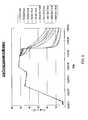
- FIGS. 5 and 5Aare simplified diagrams of a temperature profile of the furnace according to an embodiment of the present invention.
- FIGS. 6A and 6Bare simplified diagrams of a thin film copper indium diselenide device according to an embodiment of the present invention.
- FIG. 7shows exemplary furnace temperature profiles measured by in-situ thermal couples according to an embodiment of the present invention.
- FIG. 8shows exemplary temperature profile set points at various zones in a furnace according to an embodiment of the present invention.
- FIG. 9shows an exemplary furnace temperature profile and substrate temperature uniformity according to an embodiment of the present invention.
- FIG. 10shows an exemplary cell open-circuit voltage distribution from ten substrates in a furnace according to an embodiment of the present invention.
- the present inventionrelates generally to photovoltaic techniques. More particularly, the present invention provides a method and structure for a thin film photovoltaic device using a copper indium diselenide species (CIS), copper indium gallium diselenide species (CIGS), and/or others.
- CIScopper indium diselenide species
- CGScopper indium gallium diselenide species
- the inventioncan be applied to photovoltaic modules, flexible sheets, building or window glass, automotive, and others.
- FIG. 1is a simplified diagram of a transparent substrate with an overlying electrode layer according to an embodiment of the present invention.
- structure 100includes a transparent substrate 104 .
- substrate 104can be a glass substrate, for example, a soda lime glass.
- substratesinclude borosilicate glass, acrylic glass, sugar glass, specialty CorningTM glass, and others.
- a contact layer comprising a metal electrode layer 102is deposited upon substrate 104 .
- the metal electrode layer 102comprises metal material that is characterized by a predetermined conductivity that is optimized for thin-film based solar cell applications.
- the metal electrode layer 102may be deposited in various ways.
- the metal electrode layer 102comprises primarily a film of molybdenum that is deposited by sputtering.
- the thickness of the electrode layer 102may range from 200 to 700 ⁇ m.
- a sputtering apparatussuch as a DC magnetron sputtering apparatus, can be used to deposit a thin film of materials upon a substrate. Such apparatus is well known and commercially available. But it is to be understood that other types of equipments and/or processes, such as evaporation in vacuum based environment may be used as well. As an example, the sputtering deposition process is described below.
- Sputter depositionis a physical vapor deposition (PVD) method of depositing thin films by sputtering, or ejecting, material from a “target”, or source, which then deposits onto a substrate, such as a silicon wafer or glass.
- PVDphysical vapor deposition
- Sputtered atoms ejected from the targethave a wide energy distribution, typically up to 10's of eV's (100000 K). The entire range from high-energy ballistic impact to low-energy thermalized motion is accessible by changing the background gas pressure.
- the sputtering gasis often an inert gas such as argon.
- the atomic weight of the sputtering gasshould be close to the atomic weight of the target, so for sputtering light elements neon is preferable, while for heavy elements krypton or xenon are used.
- Reactive gasescan also be used to sputter compounds.
- the compoundcan be formed on the target surface, in-flight or on the substrate depending on the process parameters. The availability of many parameters that control sputter deposition make it a complex process, but also allow experts a large degree of control over the growth and microstructure of the film.
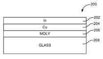
- FIG. 2is a simplified diagram of a composite structure including copper and indium material according to an embodiment of the present invention.
- structure 200is includes a glass substrate 208 , preferably soda lime glass, which is about 1 to 3 millimeters thick.
- the glass substrate 208serves as a supporting layer.
- the metal layer 206is deposited upon substrate 208 .
- the metal layer 206serves as a metal electrode layer to provide electrical contact.
- the layer 206comprises primarily a film of molybdenum which has been deposited by sputtering to a thickness of from 200 to 700 nm.
- an initial film of chromiumis first deposited upon glass 208 .
- the chromiumis used to insure good adhesion of the overall structure to the substrate 208 .
- Other types of materialmay also be used in a barrier layer, such as silicon dioxide, silicon nitride, etc.
- Layers 204 and 202include primarily a copper layer and an indium layer deposited upon metal layer 206 by a sputtering process. As shown in FIG. 2 , the indium layer overlays the copper layer. But it is to be understood that other arrangements are possible. In another embodiment, the copper layer overlays the indium layer.
- a sputtering apparatussuch as a DC magnetron sputtering apparatus, is used to deposit the thin film (e.g., layer 202 , 204 , and/or 206 ) of materials upon a substrate.
- a sputtering apparatussuch as a DC magnetron sputtering apparatus
- Such apparatusis well known and commercially available.
- Other materialcan also be used.
- techniques described throughout the present applicationare flexible and that other types of equipments and/or processes, such as evaporation in vacuum based environment may be used as well for depositing copper and indium material.
- gallium material(not shown in FIG. 2 ) may be formed deposited in addition to the copper and indium material.
- the ratio between the copper and indium+gallium materialis less than 1 (e.g., Cu/III ⁇ 0.92 ⁇ 0.96, here III means group III); that is, less than one part of copper per one part of indium material.
- the structure 200is formed by processing the structure 100 .
- the Cu and Inare deposited onto the structure 100 to form the structure 200 .
- sputtering processis used for forming the copper and/or indium layer.
- the Cu film and the In filmare shown as two separate layers.
- a Cu/In composite or Cu/In alloyis formed during the sputtering process, as shown in FIG. 2A .
- gallium material(not shown in FIG. 2 ) may be formed deposited in addition to the copper and indium material
- FIG. 2Ais a simplified diagram of a composite structure 210 including a copper and indium composite film according to another embodiment of the present invention.
- the structure 210includes a transparent substrate 216 .
- substrate 216can be a glass substrate, for example, a soda lime glass.
- a back contactcomprises a metal electrode layer 214 is deposited upon substrate 216 .
- the layer 214comprises primarily a film of molybdenum material is deposited by sputtering.
- an initial film of chromiumis deposited upon glass 216 before depositing the molybdenum material to provide for good adhesion of the overall structure to the substrate 210 .
- the layer 212comprises primarily a copper (and gallium) indium alloy or copper (gallium) indium composite material.
- a copper (or CuGa alloy) indium alloy materialis formed from separate layers of copper (or CuGa alloy) material and indium material, which diffuse into each layer.
- the process of forming of copper indium (or CuInGa) alloy materialis performed by subjecting the structure to a high temperature annealing in an environment containing gaseous selenium species.
- FIG. 3is a simplified diagram of a furnace according to an embodiment of the present invention. This diagram is merely an example, which should not limit the scope of the claims herein.
- a furnace 300includes a process chamber 302 and an end cap 304 .
- the reaction chamber 302is characterized by a volume of more than 200 liters.
- the furnace 300includes a vacuum-pumping machine that comprises a turbo molecular pump 310 and a rotary pump 312 .
- the vacuum-pumping machinecan be implemented by way of a combination of a mechanical booster pump and a dry pump.
- the raw material gas and/or a diluting gas such as helium, nitrogen, argon, or hydrogencan be introduced in process chamber 302 via a gas injection pipe 314 , if demanded by the specific applications and/or processes.
- the chamber 302is evacuated by the turbo molecular pump 310 via the rotary pump 312 that is connected with a manifold 316 via a gate valve and a conductance valve 318 .
- a heating element 306is mounted outside the reaction chamber 302 .
- the end cap 304 of the chamberis a lid with embedded temperature control elements.
- the lidis built with lamps for generating heat and cooling water pipes for actual temperature control.
- the lidalso includes quartz baffles (not shown) that serves an element for controlling exchange of heat and mass (gases) between a main spatial region of the chamber 302 and a spatial region surrounding the lid.
- the furnace 300can be used for many applications. According to an embodiment, the furnace 300 is used to apply thermal energy to various types of substrates and to introduce various types of gaseous species, among others.
- one or more glass plates or substratesare positioned vertically near the center of chamber 302 .
- substrates 308can be similar to those described in FIGS. 2 and 2A (e.g., Cu/In layers or composite Cu/In layer overlying a metal contact layer on a substrate). These layers placed in the process chamber in the presence of a gas containing selenium, such as hydrogen selenide H 2 Se. After annealing the material for a given period of time, the copper, indium and selenium interdiffuse and react to form a high quality copper indium diselenide (CIS) film.
- CIScopper indium diselenide
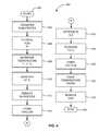
- FIG. 4is a simplified diagram of a process for forming a copper indium diselenide layer according to an embodiment of the present invention.
- This diagramis merely an example, which should not limit the scope of the claims herein.
- One of ordinary skill in the artwould recognize many other variations, modifications, and alternatives. It is also understood that the examples and embodiments described herein are for illustrative purposes only and that various modifications or changes in light thereof will be suggested to persons skilled in the art and are to be included within the spirit and purview of this process and scope of the appended claims.
- the present methodcan be briefly outlined below.
- the method 400begins at start, step 402 .
- the user of the methodbegins at a process chamber, such as the one noted above, as well as others.
- the process chambercan be maintained at about room temperature before proceeding with the present method. But the process chamber can start temperature ramping from a temperature higher than room temperature, such as 100° C.
- a plurality of substratesis transferred into the process chamber, step 402 .
- Each of the plurality of substratescan be provided in a vertical orientation with respect to gravity.
- the plurality of substratescan be defined by a number N, where N is greater than 5.
- the plurality of substratescan comprise 5 or more individual substrates.
- the plurality of substratescan comprise 40 or more individual substrates.
- each substratecan have a dimension of 65 cm ⁇ 165 cm or smaller. But it is understood that other dimensions are possible.
- Each of the substratesis maintained in substantially a planar configuration free from warp or damage.
- the gravitational forcecould cause the substrates to sag and warp unless they are placed on a supporting structure such as shelves. This occurs when the substrate material reaches a softening temperature, compromising the structural integrity of the substrate.
- glass substratesparticular soda lime glass substrates, begin to soften at 480° C.
- the substratesare also separate from one another according to a predetermined spacing to ensure even heating and reactions with gaseous species that are to be introduced to the furnace.
- gaseous speciesincluding a selenide species, and/or a carrier gas, are introduced into the process chamber in step 406 .
- the gaseous speciesincludes at least H 2 Se and nitrogen.
- the gaseous speciesother types of chemically inert gas, such as helium, argon, etc.
- the substratesare placed in the presence of a gas containing selenium, such as H 2 Se.
- step 408The furnace is then heated up to a second temperature ranging from about 350° C. to 450° C. in step 408 .
- the transfer of thermal energy for the purpose of heating the process chambercan be done by heating elements, heating coils, and the like.
- step 408at least starts the formation of a copper indium diselenide film by reactions between the gaseous species and the copper and indium composite (or layered) structure on each of the substrates.
- separate layers of copper and indium materialare diffused into each other to corm a single layer of copper indium alloy material.
- the second temperatureis maintained for 10 to 90 minutes at the heat treatment interval between 350° C. and 450° C., step 410 .
- the second temperature rangecan be from 390° C. to 410° C.
- the period of time for maintaining the temperature at step 410is provided to allow formation of the CIS film material.
- the pressure inside the furnacemay increase as well.
- a pressure release valveis used to keep the pressure within the furnace at approximately 650 torr.
- the removal of the residual selenide speciesbegins, in step 412 .
- a vacuumis formed in the process chamber through a vacuum pump, in step 414 .
- a sulfide speciesis introduced, in step 416 .
- the residual selenide removal processmay continue until the process chamber is in vacuum configuration.
- an optional stepmay include waiting before the temperature is ramped up to allow the temperature uniformity to improve for all substrates in the main spatial region of the chamber.
- the sulfide speciesis introduced with nitrogen, which functions as a carrier gas occupying approximately 70 to 75% of furnace.
- the temperature of the furnaceis increased to a third temperature ranging from about 500° C. to 525° C.
- the third temperatureis calibrated for reaction between the sulfide species and the substrates in furnace.
- step 420temperature is maintained at the third temperature for a period of time until the formation of the copper indium diselenide CIS (or CIGS if gallium is included) layer is completed.
- the stepis set up for the purpose of extracting out one or more selenium species from the copper indium diselenide film in the ambient of the furnace comprising the sulfur species. It is to be appreciated that a predetermined amount of selenium are removed. In a specific embodiment, approximately 5% of the selenium is removed from the CIS film and is replaced by about 5% of sulfur. According to an embodiment, a complete reaction between the selenium with the CIS film is desired. After the removal of residual selenium, a controlled temperature ramp down process is initiated, in step 422 .
- the furnaceis cooled to the first temperature of about room temperature, and the remaining gaseous species are removed from the furnace, in step 424 .
- the gaseous speciesare removed by a vacuum pumping machine.
- the temperature sequence described abovecan be illustrated in the temperature profile in FIG. 5 .
- step 420additional steps may be performed depending on the desired end product. For example, if a CIS or CIGS type of thin-film solar cell is desired, additional processes are provided to provide additional structures, such as a transparent layer of material such as ZnO overlaying the CIS layer.
- FIG. 5is a simplified diagram of a temperature profile of the furnace according to an embodiment of the present invention. This diagram is merely an example, which should not limit the scope of the claims herein.
- the temperature profilefurther details the temperature ramping process in the above-described method outline ( FIG. 4 ) and specification.
- An optimized temperature profile( FIG. 5 ) is provided to illustrate a heating process according to an embodiment of the present invention.
- the process chamberis configured to include independently controlled temperature zones with heater elements properly disposed near the corresponding zones. This enables the derivation of the optimized temperature profile.
- the optimized profileregulates the process chamber in order to prevent the warping of large substrates at high temperatures. If the temperature is ramped up too high too quickly, warping or damage may occur due to the softening of glass.
- the total amount of thermal energyis determined in consideration of total thermal budget available to the substrates and to maintain the uniformity and structure integrity of the glass substrate. For example, by periodically controlling the temperature of the heating process in steps, the substrate stays at a level of stabilization and relaxing in which the requisite structure integrity is maintained. As explained above, material such as glass tends to deform at a temperature of 480° C. or higher, and thus caution is exercised to avoid prolong exposure of substrate at high temperatures. Referring to FIG. 5 , while the ambience of a process chamber is maintained with a gaseous species including a selenide species and a carrier gas, a plurality of substrates is put into the furnace.
- a gaseous speciesincluding a selenide species and a carrier gas
- the plurality of substratesis provided in a vertical orientation with respect to a direction of gravity, with the plurality of substrates being defined by a number N, where N is greater than 5. In certain implementation, the number N is greater than 40.
- the substratesinclude glass substrates, such as soda lime glass.
- the furnacestarts the process with a first temperature of about 30° C. (i.e., around room temperature). The furnace of course can start with a higher temperature, such as 100° C. The furnace is then heated up to a second temperature ranging from about 350° C. to 450° C.
- the second temperatureis maintained for 10 to 90 minutes at the heat treatment interval between 350° C. to 450° C.
- the size of glass substratecan be 65 cm ⁇ 165 cm or smaller.
- a challenge in processing large substrateis the warping of the substrate at high temperatures. If the temperature is ramped up directly to T 3 , warping or damage may occur.
- all substratesare loaded in a substrate holder or boat that sets them in substantially a planar configuration free of warp or damage.
- each substrateis disposed in the boat in substantially vertical direction relative to gravity and has a predetermined spacing from its nearest neighbor. As shown in FIG. 5 , the slope of ramping up from T 2 to T 3 is calibrated to reduce and/or eliminate the risk of damaging the substrate.
- the substratecan relax and stabilize.
- the maintaining time at this intervalis set up according to the purpose of at least initiating formation of the copper indium diselenide film from the copper and indium composite structure on each of the substrates.
- the ambient of the furnaceis changed such that the selenide species is removed and a sulfide species is introduced.
- a second temperature ramp up processis initiated. There can be a delay in the ramp of furnace temperature in order to improve substrate temperature uniformity. Then, the temperature of the furnace is increased to a third temperature ranging from about 500° C. to 525° C.
- the temperature of the furnaceis maintained for 10 to 60 minutes at the heat treatment interval between 500° C. and 525° C.
- the time interval with the temperature in a plateau in an ambient comprising a sulfur species, e.g., hydrogen sulfide gas,is set up for the purpose of extracting out one or more selenium species from the copper indium diselenide film.
- the residual selenide speciescan be thermally cranked or decomposed to elemental selenium particles, which can be carried away by a convective current from relative hot main spatial region of the chamber to a relative cold region such as the end cap region.
- an exchange reactionoccurs to replace sulfur species for the selenium species in the film overlying the substrate.
- a predetermined amounte.g., 5 to 10%
- seleniumcan be extracted to provide a proper amount of selenium concentration within the CIS film.
- a controlled temperature ramp-down processis initiated, as the furnace is then cooled to the first temperature of about room temperature.
- the cooling processis specifically calibrated. As a result of this process, the copper, indium, and selenium interdiffuse and react to form a high quality copper indium diselenide film.
- FIG. 5Ais a simplified diagram of a temperature profile of the furnace according to an embodiment of the present invention. This diagram is merely an example, which should not limit the scope of the claims herein.
- the temperature profilefurther details the temperature ramping process in the above-described method outline ( FIG. 4 ) and specification.
- An optimized temperature profile ( FIG. 5A )is provided to illustrate a heating process according to an embodiment of the present invention.
- T 1is approximately set at room temperature. But it can be set as high as 100° C. At this temperature, substrates are loaded into a furnace. Air is pumped out (e.g., by vacuum device) from the furnace, and H 2 Se and N 2 gas species are introduced into the furnace. For example, these gas species are introduced to the furnace so that at pressure of approximate 650 torr is reached.
- the rate of temperature ramping upis optimized to allow the relative uniform reaction between selenium and copper and indium (and possibly with addition of gallium).
- the T 2 temperatureis approximately between 350° C. and 450° C.
- the furnacestays at the T 2 temperature for about 10 to 60 minutes.
- the time staying at the T 2 temperatureis to allow for reaction between selenium and copper indium material.
- separate layers of copper and indium materialform copper indium alloy while reacting with selenium material.
- CIS and/or CIGS materialis formed at T 2 .
- the pressure inside the furnaceis controlled to sustain a relative uniform pressure level of approximate 650 torr.
- a gas escape valveis used to release gases when the furnace heat up, where pressure increases due to gas expansion at high temperature.
- the sulfide gasalong with certain inert gases (e.g., nitrogen, argon, helium, etc.) is introduced to the furnace, and the temperature inside the furnace increases from T 2 to T 3 .
- certain inert gasese.g., nitrogen, argon, helium, etc.
- T 3is approximately 500° C. to 550° C.
- the temperaturestays at T 3 to allow the sulfide gas to interact with the CIGS and/or CIS material.
- the sulfurreplaces approximately 3 to 10% of the selenium material from the CIGS and/or CIS material.
- the furnaceis cools down in the ambient of sulfide gas which is removed at last.
- FIG. 7shows exemplary furnace temperature profiles measured by in-situ thermal couples according to an embodiment of the present invention.
- This diagramis merely an example, which should not limit the scope of the claims herein.
- a large furnaceis chosen to be the process chamber where a plurality of substrates has been loaded.
- Temperature sensorsare pre-installed for monitoring all substrates on bottom, middle, and top regions.
- FIG. 7just shows the measured temperature profile during an actual processing run. It schematically illustrates realization of the temperature profile preset in FIG. 5 or FIG. 5A .
- FIG. 7shows exemplary furnace temperature profiles measured by in-situ thermal couples according to an embodiment of the present invention.
- the furnace temperature profileis controlled by adjusting the heaters surrounding the process chamber.
- the temperature distributionmay not be plainly uniform. In fact, several temperature zones can be identified through an experiment. Therefore, the temperature profile set point for corresponding zones can be separately controlled in order to achieve an actual temperature profile with improved uniformity.
- FIG. 8just shows exemplary temperature profile set points at various zones in a furnace according to an embodiment of the present invention.
- FIG. 9shows exemplary furnace temperature profile and substrate temperature uniformity according to an embodiment of the present invention.
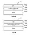
- FIG. 6is a simplified diagram of a thin film copper indium diselenide device according to an embodiment of the present invention.
- structure 600is supported on a glass substrate 610 .
- the glass substratecomprises soda lime glass, which is about 1 to 3 millimeters thick.
- a back contact including a metal layer 608is deposited upon substrate 610 .
- layer 608comprises primarily a film of molybdenum which has been deposited by sputtering.
- the first active region of the structure 600comprises a semiconductor layer 606 .
- the semiconductor layerincludes p-type copper indium diselenide (CIS) material.
- CIScopper indium diselenide
- the second active portion of the structure 600comprises layers 604 and 602 of n-type semiconductor material, such as CdS or ZnO.
- CdS and/or ZnO layersfunction as a winder layers.
- ZnOis shown overlaying the CdS layer.
- the ZnO layer 602overlays another ZnO layer that is characterized by a different resistivity.
- a photovoltaic cell, or solar cell, such as device 600 described above,is configured as a large-area p-n junction.
- the photonsmay be reflected, pass through the transparent electrode layer, or become absorbed.
- the semiconductor layerabsorbs the energy causing electron-hole pairs to be created.
- a photonneeds to have greater energy than that of the band gap in order to excite an electron from the valence band into the conduction band. This allows the electrons to flow through the material to produce a current.
- the complementary positive charges, or holesflow in the direction opposite of the electrons in a photovoltaic cell.
- a solar panel having many photovoltaic cellscan convert solar energy into direct current electricity.
- CIScopper indium diselenide
- the present inventionprovides methods for making CIS-based and/or CIGS-based solar cells on a large glass substrate for a solar panel.
- the device structure described in FIG. 6can be patterned into individual solar cells on the glass substrate and interconnected to form the solar panel.
- the present inventionthus provides a cost-effective method for making thin film solar cell panel.
- FIG. 10shows an exemplary cell open-circuit voltage distribution from ten substrates in a furnace according to an embodiment of the present invention.
- This diagramis merely an example, which should not limit the scope of the claims herein.
- 10 soda lime glass substrateshave been loaded into a furnace described before and been carried out a series of large scale selenization and sufurization processes for forming a CIS based photovoltaic absorber film.
- a key parameter, cell open-circuit voltages Vocis measured around 0.5 V for cells made from those films out of the 10 substrates.
- FIG. 10just shows that the Voc value distribution has achieved desired uniformity across all substrates in this large scale production process.
Landscapes
- Photovoltaic Devices (AREA)
- Physical Vapour Deposition (AREA)
Abstract
Description
- This application is a division of U.S. patent application Ser. No. 12/568,641 filed on Sep. 28, 2009, which claims priority to U.S. Provisional Patent Application No. 61/101,567, filed Sep. 30, 2008, entitled “THERMAL MANAGEMENT AND METHOD FOR LARGE SCALE PROCESSING OF CIS AND/OR CIGS BASED THIN FILMS OVERLYING GLASS SUBSTRATES”, the disclosures of which are incorporated by reference herein in their entirety for all purposes.
- The present invention relates generally to photovoltaic techniques. More particularly, the present invention provides a method and structure for a thin film photovoltaic device using a copper indium diselenide species (CIS), copper indium gallium diselenide species (CIGS), and/or others. The invention can be applied to photovoltaic modules, flexible sheets, building or window glass, automotive, and others.
- In the process of manufacturing CIS and/or CIGS types of thin films, there are various manufacturing challenges, such as maintaining structure integrity of substrate materials, ensuring uniformity and granularity of the thin film material, etc. While conventional techniques in the past have addressed some of these issues, they are often inadequate in various situations. Therefore, it is desirable to have improved systems and method for manufacturing thin film photovoltaic devices.
- The present invention relates generally to photovoltaic techniques. More particularly, the present invention provides a method and structure for a thin film photovoltaic device using a copper indium diselenide species (CIS), copper indium gallium diselenide species (CIGS), and/or others. The invention can be applied to photovoltaic modules, flexible sheets, building or window glass, automotive, and others.
- According to an embodiment, the present invention provides a method for fabricating a copper indium diselenide semiconductor film. The method includes providing a plurality of substrates, each of the substrates having a copper and indium composite structure. The method also includes transferring the plurality of substrates into a furnace, each of the plurality of substrates provided in a vertical orientation with respect to a direction of gravity, the plurality of substrates being defined by a number N, where N is greater than 5. The method further includes introducing a gaseous species including a selenide species and a carrier gas into the furnace and transferring thermal energy into the furnace to increase a temperature from a first temperature to a second temperature, the second temperature ranging from about 350° C. to about 450° C. to at least initiate formation of a copper indium diselenide film from the copper and indium composite structure on each of the substrates. The method additionally includes maintaining the temperature at about the second temperature for a period of time. The method also includes removing at least the residual selenide species from the furnace. The method further includes introducing a sulfide species into the furnace. The method also includes increasing a temperature to a third temperature, the third temperature ranging from about 500 to 525° C. while the plurality of substrates are maintained in an environment including a sulfur species to extract out one or more selenium species from the copper indium diselenide film.
- It is to be appreciated that the present invention provides numerous benefits over conventional techniques. Among other things, the systems and processes of the present invention are compatible with conventional systems, which allow cost effective implementation. In various embodiments, the temperature control method maintains structure integrity of substrates while providing allows various reactions to occur. There are other benefits as well.
FIG. 1 is a simplified diagram of a transparent substrate with an overlying electrode layer according to an embodiment of the present invention;FIGS. 2 and 2A are simplified diagram of a composite structure including a copper and indium film according to an embodiment of the present invention;FIG. 3 is a simplified diagram of a furnace according to an embodiment of the present invention;FIG. 4 is a simplified diagram of a process for forming a copper indium diselenide layer according to an embodiment of the present invention;FIGS. 5 and 5A are simplified diagrams of a temperature profile of the furnace according to an embodiment of the present invention; andFIGS. 6A and 6B are simplified diagrams of a thin film copper indium diselenide device according to an embodiment of the present invention.FIG. 7 shows exemplary furnace temperature profiles measured by in-situ thermal couples according to an embodiment of the present invention.FIG. 8 shows exemplary temperature profile set points at various zones in a furnace according to an embodiment of the present invention.FIG. 9 shows an exemplary furnace temperature profile and substrate temperature uniformity according to an embodiment of the present invention.FIG. 10 shows an exemplary cell open-circuit voltage distribution from ten substrates in a furnace according to an embodiment of the present invention.- The present invention relates generally to photovoltaic techniques. More particularly, the present invention provides a method and structure for a thin film photovoltaic device using a copper indium diselenide species (CIS), copper indium gallium diselenide species (CIGS), and/or others. The invention can be applied to photovoltaic modules, flexible sheets, building or window glass, automotive, and others.
FIG. 1 is a simplified diagram of a transparent substrate with an overlying electrode layer according to an embodiment of the present invention. This diagram is merely an example, which should not limit the scope of the claims herein. As shown,structure 100 includes atransparent substrate 104. In an embodiment,substrate 104 can be a glass substrate, for example, a soda lime glass. However, other types of substrates can also be used. Examples of substrates include borosilicate glass, acrylic glass, sugar glass, specialty Corning™ glass, and others. As shown, a contact layer comprising ametal electrode layer 102 is deposited uponsubstrate 104. According to an embodiment, themetal electrode layer 102 comprises metal material that is characterized by a predetermined conductivity that is optimized for thin-film based solar cell applications. Depending on the application, themetal electrode layer 102 may be deposited in various ways. For example, themetal electrode layer 102 comprises primarily a film of molybdenum that is deposited by sputtering. For example, the thickness of theelectrode layer 102 may range from 200 to 700 μm. A sputtering apparatus, such as a DC magnetron sputtering apparatus, can be used to deposit a thin film of materials upon a substrate. Such apparatus is well known and commercially available. But it is to be understood that other types of equipments and/or processes, such as evaporation in vacuum based environment may be used as well. As an example, the sputtering deposition process is described below.- Sputter deposition is a physical vapor deposition (PVD) method of depositing thin films by sputtering, or ejecting, material from a “target”, or source, which then deposits onto a substrate, such as a silicon wafer or glass. Sputtered atoms ejected from the target have a wide energy distribution, typically up to 10's of eV's (100000 K). The entire range from high-energy ballistic impact to low-energy thermalized motion is accessible by changing the background gas pressure. The sputtering gas is often an inert gas such as argon. For efficient momentum transfer, the atomic weight of the sputtering gas should be close to the atomic weight of the target, so for sputtering light elements neon is preferable, while for heavy elements krypton or xenon are used. Reactive gases can also be used to sputter compounds. The compound can be formed on the target surface, in-flight or on the substrate depending on the process parameters. The availability of many parameters that control sputter deposition make it a complex process, but also allow experts a large degree of control over the growth and microstructure of the film.
FIG. 2 is a simplified diagram of a composite structure including copper and indium material according to an embodiment of the present invention. This diagram is merely an example, which should not limit the scope of the claims herein. In this embodiment,structure 200 is includes aglass substrate 208, preferably soda lime glass, which is about 1 to 3 millimeters thick. For example, theglass substrate 208 serves as a supporting layer. Themetal layer 206 is deposited uponsubstrate 208. For example, themetal layer 206 serves as a metal electrode layer to provide electrical contact. For example, thelayer 206 comprises primarily a film of molybdenum which has been deposited by sputtering to a thickness of from 200 to 700 nm. In a specific embodiment, an initial film of chromium is first deposited uponglass 208. For example, the chromium is used to insure good adhesion of the overall structure to thesubstrate 208. Other types of material may also be used in a barrier layer, such as silicon dioxide, silicon nitride, etc.Layers metal layer 206 by a sputtering process. As shown inFIG. 2 , the indium layer overlays the copper layer. But it is to be understood that other arrangements are possible. In another embodiment, the copper layer overlays the indium layer. As an example, a sputtering apparatus, such as a DC magnetron sputtering apparatus, is used to deposit the thin film (e.g.,layer FIG. 2 ) may be formed deposited in addition to the copper and indium material. According to an embodiment, the ratio between the copper and indium+gallium material is less than 1 (e.g., Cu/III<0.92˜0.96, here III means group III); that is, less than one part of copper per one part of indium material.- As an example, the
structure 200 is formed by processing thestructure 100. For example, the Cu and In are deposited onto thestructure 100 to form thestructure 200. As described, sputtering process is used for forming the copper and/or indium layer. In the embodiment illustrated inFIG. 2 , the Cu film and the In film are shown as two separate layers. In another embodiment, a Cu/In composite or Cu/In alloy is formed during the sputtering process, as shown inFIG. 2A . It is to be appreciated that techniques described throughout the present application are flexible and that other types of equipments and/or processes, such as evaporation in vacuum based environment may be used as well for depositing copper and indium material. In certain embodiments, gallium material (not shown inFIG. 2 ) may be formed deposited in addition to the copper and indium material FIG. 2A is a simplified diagram of acomposite structure 210 including a copper and indium composite film according to another embodiment of the present invention. This diagram is merely an example, which should not limit the scope of the claims herein. As shown, thestructure 210 includes atransparent substrate 216. In an embodiment,substrate 216 can be a glass substrate, for example, a soda lime glass. A back contact comprises ametal electrode layer 214 is deposited uponsubstrate 216. For example, thelayer 214 comprises primarily a film of molybdenum material is deposited by sputtering. In a specific embodiment, an initial film of chromium is deposited uponglass 216 before depositing the molybdenum material to provide for good adhesion of the overall structure to thesubstrate 210. Thelayer 212 comprises primarily a copper (and gallium) indium alloy or copper (gallium) indium composite material. For example, the mixing or alloying of copper indium results in an improved homogeneity or advantageous morphology of the composite copper and indium film. This improved structure is carried over into the desired CIS film after the selenization step. According to an embodiment, a copper (or CuGa alloy) indium alloy material is formed from separate layers of copper (or CuGa alloy) material and indium material, which diffuse into each layer. For example, the process of forming of copper indium (or CuInGa) alloy material is performed by subjecting the structure to a high temperature annealing in an environment containing gaseous selenium species.FIG. 3 is a simplified diagram of a furnace according to an embodiment of the present invention. This diagram is merely an example, which should not limit the scope of the claims herein. As shown, afurnace 300 includes aprocess chamber 302 and anend cap 304. According to an embodiment, thereaction chamber 302 is characterized by a volume of more than 200 liters. As shown inFIG. 3 , thefurnace 300 includes a vacuum-pumping machine that comprises a turbomolecular pump 310 and arotary pump 312. Depending on the application, the vacuum-pumping machine can be implemented by way of a combination of a mechanical booster pump and a dry pump. For example, the raw material gas and/or a diluting gas such as helium, nitrogen, argon, or hydrogen can be introduced inprocess chamber 302 via agas injection pipe 314, if demanded by the specific applications and/or processes. Thechamber 302 is evacuated by the turbomolecular pump 310 via therotary pump 312 that is connected with a manifold316 via a gate valve and aconductance valve 318. For example, there are no special partitions in the manifold or in the reaction furnaces. Aheating element 306 is mounted outside thereaction chamber 302.- In a specific embodiment, the
end cap 304 of the chamber is a lid with embedded temperature control elements. For example, the lid is built with lamps for generating heat and cooling water pipes for actual temperature control. The lid also includes quartz baffles (not shown) that serves an element for controlling exchange of heat and mass (gases) between a main spatial region of thechamber 302 and a spatial region surrounding the lid. By controlling the lid temperature through the embedded elements and heat/mass flow through the baffles, the reactive chemistry in the main spatial region of the chamber, where the substrates with copper indium gallium composite film are loaded, is under controlled. - The
furnace 300 can be used for many applications. According to an embodiment, thefurnace 300 is used to apply thermal energy to various types of substrates and to introduce various types of gaseous species, among others. In an embodiment, one or more glass plates or substrates are positioned vertically near the center ofchamber 302. As an example,substrates 308 can be similar to those described inFIGS. 2 and 2A (e.g., Cu/In layers or composite Cu/In layer overlying a metal contact layer on a substrate). These layers placed in the process chamber in the presence of a gas containing selenium, such as hydrogen selenide H2Se. After annealing the material for a given period of time, the copper, indium and selenium interdiffuse and react to form a high quality copper indium diselenide (CIS) film. FIG. 4 is a simplified diagram of a process for forming a copper indium diselenide layer according to an embodiment of the present invention. This diagram is merely an example, which should not limit the scope of the claims herein. One of ordinary skill in the art would recognize many other variations, modifications, and alternatives. It is also understood that the examples and embodiments described herein are for illustrative purposes only and that various modifications or changes in light thereof will be suggested to persons skilled in the art and are to be included within the spirit and purview of this process and scope of the appended claims.- As shown in
FIG. 4 , the present method can be briefly outlined below. - 1. Start;
- 2. Provide a plurality of substrates having a copper and indium composite structure
- 3. Introduce a gaseous species including a selenide species and a carrier gas into the furnace;
- 4. Transfer thermal energy into the furnace to increase a temperature from a first temperature to a second temperature;
- 5. Maintain the temperature at about the second temperature for a period of time;
- 6. Remove at least the residual selenide species from the furnace;
- 7. Form vacuum in the process chamber;
- 8. Introduce a sulfide species into the furnace while;
- 9. Increasing the temperature to a third temperature;
- 10. Maintain the temperature at about the third temperature for a period of time;
- 11. Ramp down the temperature from the third temperature to about the first temperature;
- 12. Remove gas; and
- 13. Stop.
- These steps are merely examples and should not limit the scope of the claims herein. One of ordinary skill in the art would recognize many other variations, modifications, and alternatives. For example, various steps outlined above may be added, removed, modified, rearranged, repeated, and/or overlapped, as contemplated within the scope of the invention. As shown, the
method 400 begins at start,step 402. Here, the user of the method begins at a process chamber, such as the one noted above, as well as others. The process chamber can be maintained at about room temperature before proceeding with the present method. But the process chamber can start temperature ramping from a temperature higher than room temperature, such as 100° C. - A plurality of substrates is transferred into the process chamber,
step 402. Each of the plurality of substrates can be provided in a vertical orientation with respect to gravity. The plurality of substrates can be defined by a number N, where N is greater than 5. The plurality of substrates can comprise 5 or more individual substrates. In another embodiment, the plurality of substrates can comprise 40 or more individual substrates. For example, each substrate can have a dimension of 65 cm×165 cm or smaller. But it is understood that other dimensions are possible. Each of the substrates is maintained in substantially a planar configuration free from warp or damage. For example, if the substrates were provided in an orientation other than vertical with respect to gravity, the gravitational force could cause the substrates to sag and warp unless they are placed on a supporting structure such as shelves. This occurs when the substrate material reaches a softening temperature, compromising the structural integrity of the substrate. Typically, glass substrates, particular soda lime glass substrates, begin to soften at 480° C. In an embodiment, the substrates are also separate from one another according to a predetermined spacing to ensure even heating and reactions with gaseous species that are to be introduced to the furnace. - After the substrates are positioned into the process chamber, gaseous species, including a selenide species, and/or a carrier gas, are introduced into the process chamber in
step 406. In an embodiment, the gaseous species includes at least H2Se and nitrogen. In another embodiment, the gaseous species other types of chemically inert gas, such as helium, argon, etc. For example, the substrates are placed in the presence of a gas containing selenium, such as H2Se. - The furnace is then heated up to a second temperature ranging from about 350° C. to 450° C. in
step 408. The transfer of thermal energy for the purpose of heating the process chamber can be done by heating elements, heating coils, and the like. For example,step 408, among other things, at least starts the formation of a copper indium diselenide film by reactions between the gaseous species and the copper and indium composite (or layered) structure on each of the substrates. In a specific embodiment, separate layers of copper and indium material are diffused into each other to corm a single layer of copper indium alloy material. The second temperature is maintained for 10 to 90 minutes at the heat treatment interval between 350° C. and 450° C.,step 410. In another embodiment, the second temperature range can be from 390° C. to 410° C. For example, the period of time for maintaining the temperature atstep 410 is provided to allow formation of the CIS film material. As the temperature increases, the pressure inside the furnace may increase as well. In a specific embodiment, a pressure release valve is used to keep the pressure within the furnace at approximately 650 torr. - As the temperature is maintained at the second temperature (step410) or at least when the temperature above certain threshold, the removal of the residual selenide species begins, in
step 412. A vacuum is formed in the process chamber through a vacuum pump, instep 414. Once the vacuum is created in the process chamber (step414), a sulfide species is introduced, instep 416. In a specific embodiment, the residual selenide removal process may continue until the process chamber is in vacuum configuration. After the gas ambience in the furnace has been changed such that the residual selenide species is removed and the sulfide species is introduced, a second temperature ramp up process is initiated,step 418. But, an optional step may include waiting before the temperature is ramped up to allow the temperature uniformity to improve for all substrates in the main spatial region of the chamber. In a specific embodiment, the sulfide species is introduced with nitrogen, which functions as a carrier gas occupying approximately 70 to 75% of furnace. The temperature of the furnace is increased to a third temperature ranging from about 500° C. to 525° C. For example, the third temperature is calibrated for reaction between the sulfide species and the substrates in furnace. - At
step 420, temperature is maintained at the third temperature for a period of time until the formation of the copper indium diselenide CIS (or CIGS if gallium is included) layer is completed. The step is set up for the purpose of extracting out one or more selenium species from the copper indium diselenide film in the ambient of the furnace comprising the sulfur species. It is to be appreciated that a predetermined amount of selenium are removed. In a specific embodiment, approximately 5% of the selenium is removed from the CIS film and is replaced by about 5% of sulfur. According to an embodiment, a complete reaction between the selenium with the CIS film is desired. After the removal of residual selenium, a controlled temperature ramp down process is initiated, instep 422. The furnace is cooled to the first temperature of about room temperature, and the remaining gaseous species are removed from the furnace, instep 424. For example, the gaseous species are removed by a vacuum pumping machine. The temperature sequence described above can be illustrated in the temperature profile inFIG. 5 . - After
step 420, additional steps may be performed depending on the desired end product. For example, if a CIS or CIGS type of thin-film solar cell is desired, additional processes are provided to provide additional structures, such as a transparent layer of material such as ZnO overlaying the CIS layer. - It is also understood that the examples and embodiments described herein are for illustrative purposes only and that various modifications or changes in light thereof will be suggest to persons skilled in the art and are to be included within the spirit and purview of this application and scope of the appended claims.
FIG. 5 is a simplified diagram of a temperature profile of the furnace according to an embodiment of the present invention. This diagram is merely an example, which should not limit the scope of the claims herein. The temperature profile further details the temperature ramping process in the above-described method outline (FIG. 4 ) and specification. An optimized temperature profile (FIG. 5 ) is provided to illustrate a heating process according to an embodiment of the present invention. In an embodiment, the process chamber is configured to include independently controlled temperature zones with heater elements properly disposed near the corresponding zones. This enables the derivation of the optimized temperature profile. The optimized profile regulates the process chamber in order to prevent the warping of large substrates at high temperatures. If the temperature is ramped up too high too quickly, warping or damage may occur due to the softening of glass. In addition, the total amount of thermal energy is determined in consideration of total thermal budget available to the substrates and to maintain the uniformity and structure integrity of the glass substrate. For example, by periodically controlling the temperature of the heating process in steps, the substrate stays at a level of stabilization and relaxing in which the requisite structure integrity is maintained. As explained above, material such as glass tends to deform at a temperature of 480° C. or higher, and thus caution is exercised to avoid prolong exposure of substrate at high temperatures. Referring toFIG. 5 , while the ambience of a process chamber is maintained with a gaseous species including a selenide species and a carrier gas, a plurality of substrates is put into the furnace. The plurality of substrates is provided in a vertical orientation with respect to a direction of gravity, with the plurality of substrates being defined by a number N, where N is greater than 5. In certain implementation, the number N is greater than 40. In an embodiment, the substrates include glass substrates, such as soda lime glass. The furnace starts the process with a first temperature of about 30° C. (i.e., around room temperature). The furnace of course can start with a higher temperature, such as 100° C. The furnace is then heated up to a second temperature ranging from about 350° C. to 450° C.- The second temperature is maintained for 10 to 90 minutes at the heat treatment interval between 350° C. to 450° C. The size of glass substrate can be 65 cm×165 cm or smaller. A challenge in processing large substrate is the warping of the substrate at high temperatures. If the temperature is ramped up directly to T3, warping or damage may occur. In an embodiment, all substrates are loaded in a substrate holder or boat that sets them in substantially a planar configuration free of warp or damage. In an example, each substrate is disposed in the boat in substantially vertical direction relative to gravity and has a predetermined spacing from its nearest neighbor. As shown in
FIG. 5 , the slope of ramping up from T2 to T3 is calibrated to reduce and/or eliminate the risk of damaging the substrate. By maintaining the temperature in the process chamber at T2 for a period of time, the substrate can relax and stabilize. The maintaining time at this interval is set up according to the purpose of at least initiating formation of the copper indium diselenide film from the copper and indium composite structure on each of the substrates. - While the second temperature is maintained, the ambient of the furnace is changed such that the selenide species is removed and a sulfide species is introduced.
- After the gas ambient in the furnace has been changed such that the selenide species is removed and the sulfide species is introduced, a second temperature ramp up process is initiated. There can be a delay in the ramp of furnace temperature in order to improve substrate temperature uniformity. Then, the temperature of the furnace is increased to a third temperature ranging from about 500° C. to 525° C.
- After the temperature ramp-up process, the temperature of the furnace is maintained for 10 to 60 minutes at the heat treatment interval between 500° C. and 525° C. The time interval with the temperature in a plateau in an ambient comprising a sulfur species, e.g., hydrogen sulfide gas, is set up for the purpose of extracting out one or more selenium species from the copper indium diselenide film. In particular, the residual selenide species can be thermally cranked or decomposed to elemental selenium particles, which can be carried away by a convective current from relative hot main spatial region of the chamber to a relative cold region such as the end cap region. Additionally, an exchange reaction occurs to replace sulfur species for the selenium species in the film overlying the substrate. As explained above, a predetermined amount (e.g., 5 to 10%) of selenium can be extracted to provide a proper amount of selenium concentration within the CIS film.
- After partial replacement of selenium by sulfur, a controlled temperature ramp-down process is initiated, as the furnace is then cooled to the first temperature of about room temperature. According to an embodiment, the cooling process is specifically calibrated. As a result of this process, the copper, indium, and selenium interdiffuse and react to form a high quality copper indium diselenide film.
FIG. 5A is a simplified diagram of a temperature profile of the furnace according to an embodiment of the present invention. This diagram is merely an example, which should not limit the scope of the claims herein. The temperature profile further details the temperature ramping process in the above-described method outline (FIG. 4 ) and specification. An optimized temperature profile (FIG. 5A ) is provided to illustrate a heating process according to an embodiment of the present invention.- As shown in
FIG. 5A , T1 is approximately set at room temperature. But it can be set as high as 100° C. At this temperature, substrates are loaded into a furnace. Air is pumped out (e.g., by vacuum device) from the furnace, and H2Se and N2gas species are introduced into the furnace. For example, these gas species are introduced to the furnace so that at pressure of approximate 650 torr is reached. - Next temperature increases from T1 to T2 inside the furnace. For example, the rate of temperature ramping up is optimized to allow the relative uniform reaction between selenium and copper and indium (and possibly with addition of gallium). According to embodiments, the T2 temperature is approximately between 350° C. and 450° C. For example, the furnace stays at the T2 temperature for about 10 to 60 minutes. The time staying at the T2 temperature is to allow for reaction between selenium and copper indium material. In a specific embodiment, separate layers of copper and indium material form copper indium alloy while reacting with selenium material. As shown, CIS and/or CIGS material is formed at T2. During the temperature ramping up process, the pressure inside the furnace is controlled to sustain a relative uniform pressure level of approximate 650 torr. For example, a gas escape valve is used to release gases when the furnace heat up, where pressure increases due to gas expansion at high temperature.
- After the CIS or CIGS material formed, various gaseous species are again pumped out from the furnace. Then, the sulfide gas along with certain inert gases (e.g., nitrogen, argon, helium, etc.) is introduced to the furnace, and the temperature inside the furnace increases from T2 to T3. However, there can be an optional time delay in the ramp of furnace temperature in order to improve substrate temperature uniformity. For example, T3 is approximately 500° C. to 550° C. In a specific embodiment, the temperature stays at T3 to allow the sulfide gas to interact with the CIGS and/or CIS material. For example, the sulfur replaces approximately 3 to 10% of the selenium material from the CIGS and/or CIS material. After the reaction, the furnace is cools down in the ambient of sulfide gas which is removed at last.
FIG. 7 shows exemplary furnace temperature profiles measured by in-situ thermal couples according to an embodiment of the present invention. This diagram is merely an example, which should not limit the scope of the claims herein. As shown, a large furnace is chosen to be the process chamber where a plurality of substrates has been loaded. Temperature sensors are pre-installed for monitoring all substrates on bottom, middle, and top regions.FIG. 7 just shows the measured temperature profile during an actual processing run. It schematically illustrates realization of the temperature profile preset inFIG. 5 orFIG. 5A . Of course there can be many variations, modifications, and alternatives.- In an embodiment, the furnace temperature profile, as seen in
FIG. 7 , is controlled by adjusting the heaters surrounding the process chamber. Additionally, depending on the internal structural design and substrate configuration when loaded in the substrate holder or boat, the temperature distribution may not be plainly uniform. In fact, several temperature zones can be identified through an experiment. Therefore, the temperature profile set point for corresponding zones can be separately controlled in order to achieve an actual temperature profile with improved uniformity.FIG. 8 just shows exemplary temperature profile set points at various zones in a furnace according to an embodiment of the present invention. - For achieving desired cell performance for such large sized substrate (65 cm×165 cm), controlling the process with improved temperature uniformity is very important. As mentioned above, identifying various temperature zones in the furnace for setting independent temperature control is one method. Other methods of improving temperature uniformity include designing proper internal structural arrangement and substrate loading configuration. For example, adding certain baffles inside the furnace inner surface can partially isolate main processing zone for achieving better temperature uniformity and controlling the internal convective flow. Adding temperature control elements to an end cap (or lid) so that it can act as a “cryopump” inside the process chamber for reduce contamination and enhance chemistry control of the reactive annealing of the film on substrate.
FIG. 9 shows exemplary furnace temperature profile and substrate temperature uniformity according to an embodiment of the present invention. This diagram is merely an example, which should not limit the scope of the claims herein. As shown, the temperature uniformity, described by a temperature difference from bottom to top of the substrate, can be substantially improved by adding certain structural baffle to the furnace internal surface and adjusting the substrate position in the substrate loading boat. Of course, there can be many variations, modifications, and alternatives. FIG. 6 is a simplified diagram of a thin film copper indium diselenide device according to an embodiment of the present invention. This diagram is merely an example, which should not limit the scope of the claims herein. As shown,structure 600 is supported on aglass substrate 610. According to an embodiment, the glass substrate comprises soda lime glass, which is about 1 to 3 millimeters thick. A back contact including ametal layer 608 is deposited uponsubstrate 610. According to an embodiment,layer 608 comprises primarily a film of molybdenum which has been deposited by sputtering. The first active region of thestructure 600 comprises asemiconductor layer 606. In an embodiment, the semiconductor layer includes p-type copper indium diselenide (CIS) material. It is to be understood that other the semiconductor layer may include other types of material, such as CIGS, as shown. The second active portion of thestructure 600 compriseslayers FIG. 6 , ZnO is shown overlaying the CdS layer. However, it should be understood that other variations are possible. In an alternative embodiments, theZnO layer 602 overlays another ZnO layer that is characterized by a different resistivity.- A photovoltaic cell, or solar cell, such as
device 600 described above, is configured as a large-area p-n junction. When photons in sunlight hit the photovoltaic cell, the photons may be reflected, pass through the transparent electrode layer, or become absorbed. The semiconductor layer absorbs the energy causing electron-hole pairs to be created. A photon needs to have greater energy than that of the band gap in order to excite an electron from the valence band into the conduction band. This allows the electrons to flow through the material to produce a current. The complementary positive charges, or holes, flow in the direction opposite of the electrons in a photovoltaic cell. A solar panel having many photovoltaic cells can convert solar energy into direct current electricity. - Semiconductors based on the copper indium diselenide (CIS) configuration are especially attractive for thin film solar cell application because of their high optical absorption coefficients and versatile optical and electrical characteristics. These characteristics can in principle be manipulated and tuned for a specific need in a given device. Selenium allows for better uniformity across the layer and so the number of recombination sites in the film are reduced which benefits the quantum efficiency and thus the conversion efficiency.
- The present invention provides methods for making CIS-based and/or CIGS-based solar cells on a large glass substrate for a solar panel. The device structure described in
FIG. 6 can be patterned into individual solar cells on the glass substrate and interconnected to form the solar panel. The present invention thus provides a cost-effective method for making thin film solar cell panel. FIG. 10 shows an exemplary cell open-circuit voltage distribution from ten substrates in a furnace according to an embodiment of the present invention. This diagram is merely an example, which should not limit the scope of the claims herein. As shown, 10 soda lime glass substrates have been loaded into a furnace described before and been carried out a series of large scale selenization and sufurization processes for forming a CIS based photovoltaic absorber film. As the results, eventually the photovoltaic cells made from these films are tested on their IV characteristics. A key parameter, cell open-circuit voltages Voc, is measured around 0.5 V for cells made from those films out of the 10 substrates.FIG. 10 just shows that the Voc value distribution has achieved desired uniformity across all substrates in this large scale production process.- It will be appreciated that all of the benefits of the present invention can be achieved regardless of the order of deposition of the copper and indium films. That is, the indium could be deposited first or the films could be deposited as a sandwich or stack of thinner layers.
- It is also understood that the examples and embodiments described herein are for illustrative purposes only and that various modifications or changes in light thereof will be suggest to persons skilled in the art and are to be included within the spirit and purview of this application and scope of the appended claims. Although the above has been generally described in terms of a specific structure for CIS and/or CIGS thin film cells, other specific CIS and/or CIGS configurations can also be used, such as those noted in issued U.S. Pat. No. 4,611,091 and U.S. Pat. No. 4,612,411, which are hereby incorporated by reference herein, without departing from the invention described by the claims herein.
Claims (20)
Priority Applications (1)
| Application Number | Priority Date | Filing Date | Title |
|---|---|---|---|
| US12/953,674US7993954B2 (en) | 2008-09-30 | 2010-11-24 | Thermal management and method for large scale processing of CIS and/or CIGS based thin films overlying glass substrates |
Applications Claiming Priority (3)
| Application Number | Priority Date | Filing Date | Title |
|---|---|---|---|
| US10156708P | 2008-09-30 | 2008-09-30 | |
| US12/568,641US7910399B1 (en) | 2008-09-30 | 2009-09-28 | Thermal management and method for large scale processing of CIS and/or CIGS based thin films overlying glass substrates |
| US12/953,674US7993954B2 (en) | 2008-09-30 | 2010-11-24 | Thermal management and method for large scale processing of CIS and/or CIGS based thin films overlying glass substrates |
Related Parent Applications (1)
| Application Number | Title | Priority Date | Filing Date |
|---|---|---|---|
| US12/568,641DivisionUS7910399B1 (en) | 2008-09-30 | 2009-09-28 | Thermal management and method for large scale processing of CIS and/or CIGS based thin films overlying glass substrates |
Publications (2)
| Publication Number | Publication Date |
|---|---|
| US20110070682A1true US20110070682A1 (en) | 2011-03-24 |
| US7993954B2 US7993954B2 (en) | 2011-08-09 |
Family
ID=43741740
Family Applications (11)
| Application Number | Title | Priority Date | Filing Date |
|---|---|---|---|
| US12/568,641Expired - Fee RelatedUS7910399B1 (en) | 2008-09-30 | 2009-09-28 | Thermal management and method for large scale processing of CIS and/or CIGS based thin films overlying glass substrates |
| US12/953,729Expired - Fee RelatedUS8084292B2 (en) | 2008-09-30 | 2010-11-24 | Thermal management and method for large scale processing of CIS and/or CIGS based thin films overlying glass substrates |
| US12/953,725Expired - Fee RelatedUS8084291B2 (en) | 2008-09-30 | 2010-11-24 | Thermal management and method for large scale processing of CIS and/or CIGS based thin films overlying glass substrates |
| US12/953,701Expired - Fee RelatedUS8071421B2 (en) | 2008-09-30 | 2010-11-24 | Thermal management and method for large scale processing of CIS and/or CIGS based thin films overlying glass substrates |
| US12/953,697Expired - Fee RelatedUS7955891B2 (en) | 2008-09-30 | 2010-11-24 | Thermal management and method for large scale processing of CIS and /or CIGS based thin films overlying glass substrates |
| US12/953,674Expired - Fee RelatedUS7993954B2 (en) | 2008-09-30 | 2010-11-24 | Thermal management and method for large scale processing of CIS and/or CIGS based thin films overlying glass substrates |
| US12/953,716Expired - Fee RelatedUS8067263B2 (en) | 2008-09-30 | 2010-11-24 | Thermal management and method for large scale processing of CIS and/or CIGS based thin films overlying glass substrates |
| US12/953,679Expired - Fee RelatedUS7993955B2 (en) | 2008-09-30 | 2010-11-24 | Thermal management and method for large scale processing of CIS and/or CIGS based thin films overlying glass substrates |
| US12/953,708Expired - Fee RelatedUS8076176B2 (en) | 2008-09-30 | 2010-11-24 | Thermal management and method for large scale processing of CIS and/or CIGS based thin films overlying glass substrates |
| US12/953,721Expired - Fee RelatedUS8088640B2 (en) | 2008-09-30 | 2010-11-24 | Thermal management and method for large scale processing of CIS and/or CIGS based thin films overlying glass substrates |
| US13/292,718Expired - Fee RelatedUS8318531B2 (en) | 2008-09-30 | 2011-11-09 | Thermal management and method for large scale processing of CIS and/or CIGS based thin films overlying glass substrates |
Family Applications Before (5)
| Application Number | Title | Priority Date | Filing Date |
|---|---|---|---|
| US12/568,641Expired - Fee RelatedUS7910399B1 (en) | 2008-09-30 | 2009-09-28 | Thermal management and method for large scale processing of CIS and/or CIGS based thin films overlying glass substrates |
| US12/953,729Expired - Fee RelatedUS8084292B2 (en) | 2008-09-30 | 2010-11-24 | Thermal management and method for large scale processing of CIS and/or CIGS based thin films overlying glass substrates |
| US12/953,725Expired - Fee RelatedUS8084291B2 (en) | 2008-09-30 | 2010-11-24 | Thermal management and method for large scale processing of CIS and/or CIGS based thin films overlying glass substrates |
| US12/953,701Expired - Fee RelatedUS8071421B2 (en) | 2008-09-30 | 2010-11-24 | Thermal management and method for large scale processing of CIS and/or CIGS based thin films overlying glass substrates |
| US12/953,697Expired - Fee RelatedUS7955891B2 (en) | 2008-09-30 | 2010-11-24 | Thermal management and method for large scale processing of CIS and /or CIGS based thin films overlying glass substrates |
Family Applications After (5)
| Application Number | Title | Priority Date | Filing Date |
|---|---|---|---|
| US12/953,716Expired - Fee RelatedUS8067263B2 (en) | 2008-09-30 | 2010-11-24 | Thermal management and method for large scale processing of CIS and/or CIGS based thin films overlying glass substrates |
| US12/953,679Expired - Fee RelatedUS7993955B2 (en) | 2008-09-30 | 2010-11-24 | Thermal management and method for large scale processing of CIS and/or CIGS based thin films overlying glass substrates |
| US12/953,708Expired - Fee RelatedUS8076176B2 (en) | 2008-09-30 | 2010-11-24 | Thermal management and method for large scale processing of CIS and/or CIGS based thin films overlying glass substrates |
| US12/953,721Expired - Fee RelatedUS8088640B2 (en) | 2008-09-30 | 2010-11-24 | Thermal management and method for large scale processing of CIS and/or CIGS based thin films overlying glass substrates |
| US13/292,718Expired - Fee RelatedUS8318531B2 (en) | 2008-09-30 | 2011-11-09 | Thermal management and method for large scale processing of CIS and/or CIGS based thin films overlying glass substrates |
Country Status (1)
| Country | Link |
|---|---|
| US (11) | US7910399B1 (en) |
Cited By (41)
| Publication number | Priority date | Publication date | Assignee | Title |
|---|---|---|---|---|
| US20070264488A1 (en)* | 2006-05-15 | 2007-11-15 | Stion Corporation | Method and structure for thin film photovoltaic materials using semiconductor materials |
| US20080300918A1 (en)* | 2007-05-29 | 2008-12-04 | Commercenet Consortium, Inc. | System and method for facilitating hospital scheduling and support |
| US20090250105A1 (en)* | 2007-09-28 | 2009-10-08 | Stion Corporation | Thin film metal oxide bearing semiconductor material for single junction solar cell devices |
| US20090320920A1 (en)* | 2008-06-25 | 2009-12-31 | Stion Corporation | High efficiency photovoltaic cell and manufacturing method free of metal disulfide barrier material |
| US20100087027A1 (en)* | 2008-09-30 | 2010-04-08 | Stion Corporation | Large Scale Chemical Bath System and Method for Cadmium Sulfide Processing of Thin Film Photovoltaic Materials |
| US20100122726A1 (en)* | 2008-11-20 | 2010-05-20 | Stion Corporation | Method and structure for thin film photovoltaic cell using similar material junction |
| US20110020980A1 (en)* | 2008-10-01 | 2011-01-27 | Stion Corporation | Thermal pre-treatment process for soda lime glass substrate for thin film photovoltaic materials |
| US20110070687A1 (en)* | 2008-09-30 | 2011-03-24 | Stion Corporation | Thermal management and method for large scale processing of cis and/or cigs based thin films overlying glass substrates |
| US20110073181A1 (en)* | 2008-09-30 | 2011-03-31 | Stion Corporation | Patterning electrode materials free from berm structures for thin film photovoltaic cells |
| US20110212565A1 (en)* | 2008-09-30 | 2011-09-01 | Stion Corporation | Humidity Control and Method for Thin Film Photovoltaic Materials |
| US8168463B2 (en) | 2008-10-17 | 2012-05-01 | Stion Corporation | Zinc oxide film method and structure for CIGS cell |
| US8193028B2 (en) | 2008-10-06 | 2012-06-05 | Stion Corporation | Sulfide species treatment of thin film photovoltaic cell and manufacturing method |
| US8198122B2 (en) | 2008-09-29 | 2012-06-12 | Stion Corporation | Bulk chloride species treatment of thin film photovoltaic cell and manufacturing method |
| US8236597B1 (en) | 2008-09-29 | 2012-08-07 | Stion Corporation | Bulk metal species treatment of thin film photovoltaic cell and manufacturing method |
| US8258000B2 (en) | 2008-09-29 | 2012-09-04 | Stion Corporation | Bulk sodium species treatment of thin film photovoltaic cell and manufacturing method |
| US8263494B2 (en) | 2010-01-25 | 2012-09-11 | Stion Corporation | Method for improved patterning accuracy for thin film photovoltaic panels |
| US8287942B1 (en) | 2007-09-28 | 2012-10-16 | Stion Corporation | Method for manufacture of semiconductor bearing thin film material |
| US8314326B2 (en) | 2006-05-15 | 2012-11-20 | Stion Corporation | Method and structure for thin film photovoltaic materials using bulk semiconductor materials |
| US8372684B1 (en) | 2009-05-14 | 2013-02-12 | Stion Corporation | Method and system for selenization in fabricating CIGS/CIS solar cells |
| US8377736B2 (en) | 2008-10-02 | 2013-02-19 | Stion Corporation | System and method for transferring substrates in large scale processing of CIGS and/or CIS devices |
| US8394662B1 (en) | 2008-09-29 | 2013-03-12 | Stion Corporation | Chloride species surface treatment of thin film photovoltaic cell and manufacturing method |
| US8398772B1 (en) | 2009-08-18 | 2013-03-19 | Stion Corporation | Method and structure for processing thin film PV cells with improved temperature uniformity |
| US8425739B1 (en) | 2008-09-30 | 2013-04-23 | Stion Corporation | In chamber sodium doping process and system for large scale cigs based thin film photovoltaic materials |
| US8436445B2 (en) | 2011-08-15 | 2013-05-07 | Stion Corporation | Method of manufacture of sodium doped CIGS/CIGSS absorber layers for high efficiency photovoltaic devices |
| US8435826B1 (en) | 2008-10-06 | 2013-05-07 | Stion Corporation | Bulk sulfide species treatment of thin film photovoltaic cell and manufacturing method |
| US8461061B2 (en) | 2010-07-23 | 2013-06-11 | Stion Corporation | Quartz boat method and apparatus for thin film thermal treatment |
| US8476104B1 (en) | 2008-09-29 | 2013-07-02 | Stion Corporation | Sodium species surface treatment of thin film photovoltaic cell and manufacturing method |
| US8501507B2 (en) | 2007-11-14 | 2013-08-06 | Stion Corporation | Method for large scale manufacture of thin film photovoltaic devices using multi-chamber configuration |
| US8501521B1 (en) | 2008-09-29 | 2013-08-06 | Stion Corporation | Copper species surface treatment of thin film photovoltaic cell and manufacturing method |
| US8507786B1 (en) | 2009-06-27 | 2013-08-13 | Stion Corporation | Manufacturing method for patterning CIGS/CIS solar cells |
| US8617917B2 (en) | 2008-06-25 | 2013-12-31 | Stion Corporation | Consumable adhesive layer for thin film photovoltaic material |
| US8628997B2 (en) | 2010-10-01 | 2014-01-14 | Stion Corporation | Method and device for cadmium-free solar cells |
| US8642138B2 (en) | 2008-06-11 | 2014-02-04 | Stion Corporation | Processing method for cleaning sulfur entities of contact regions |
| US8691618B2 (en) | 2008-09-29 | 2014-04-08 | Stion Corporation | Metal species surface treatment of thin film photovoltaic cell and manufacturing method |
| US8728200B1 (en) | 2011-01-14 | 2014-05-20 | Stion Corporation | Method and system for recycling processing gas for selenization of thin film photovoltaic materials |
| US8809096B1 (en) | 2009-10-22 | 2014-08-19 | Stion Corporation | Bell jar extraction tool method and apparatus for thin film photovoltaic materials |
| US8859880B2 (en) | 2010-01-22 | 2014-10-14 | Stion Corporation | Method and structure for tiling industrial thin-film solar devices |
| US8871305B2 (en) | 2007-06-29 | 2014-10-28 | Stion Corporation | Methods for infusing one or more materials into nano-voids of nanoporous or nanostructured materials |
| US8941132B2 (en) | 2008-09-10 | 2015-01-27 | Stion Corporation | Application specific solar cell and method for manufacture using thin film photovoltaic materials |
| US8998606B2 (en) | 2011-01-14 | 2015-04-07 | Stion Corporation | Apparatus and method utilizing forced convection for uniform thermal treatment of thin film devices |
| US9096930B2 (en) | 2010-03-29 | 2015-08-04 | Stion Corporation | Apparatus for manufacturing thin film photovoltaic devices |
Families Citing this family (72)
| Publication number | Priority date | Publication date | Assignee | Title |
|---|---|---|---|---|
| US20110017298A1 (en)* | 2007-11-14 | 2011-01-27 | Stion Corporation | Multi-junction solar cell devices |
| US20090301562A1 (en)* | 2008-06-05 | 2009-12-10 | Stion Corporation | High efficiency photovoltaic cell and manufacturing method |
| WO2010060646A1 (en)* | 2008-11-28 | 2010-06-03 | Volker Probst | Method for producing semiconductor layers and coated substrates treated with elemental selenium and/or sulfur, in particular flat substrates |
| US20100051090A1 (en)* | 2008-08-28 | 2010-03-04 | Stion Corporation | Four terminal multi-junction thin film photovoltaic device and method |
| US8008111B1 (en) | 2008-09-29 | 2011-08-30 | Stion Corporation | Bulk copper species treatment of thin film photovoltaic cell and manufacturing method |
| US8569613B1 (en) | 2008-09-29 | 2013-10-29 | Stion Corporation | Multi-terminal photovoltaic module including independent cells and related system |
| US20100078059A1 (en)* | 2008-09-30 | 2010-04-01 | Stion Corporation | Method and structure for thin film tandem photovoltaic cell |
| US8232134B2 (en) | 2008-09-30 | 2012-07-31 | Stion Corporation | Rapid thermal method and device for thin film tandem cell |
| US8563850B2 (en)* | 2009-03-16 | 2013-10-22 | Stion Corporation | Tandem photovoltaic cell and method using three glass substrate configuration |
| FR2951022B1 (en)* | 2009-10-07 | 2012-07-27 | Nexcis | MANUFACTURE OF THIN LAYERS WITH PHOTOVOLTAIC PROPERTIES, BASED ON TYPE I-III-VI2 ALLOY, BY SUCCESSIVE ELECTRO-DEPOSITS AND THERMAL POST-TREATMENT. |
| US20120264072A1 (en)* | 2011-02-03 | 2012-10-18 | Stion Corporation | Method and apparatus for performing reactive thermal treatment of thin film pv material |
| US9234857B2 (en)* | 2011-11-14 | 2016-01-12 | First Solar, Inc. | Method and apparatus providing temperature uniformity |
| TWI456779B (en)* | 2011-12-28 | 2014-10-11 | Ind Tech Res Inst | Modification method of light absorbing layer |
| TWI475713B (en)* | 2012-05-16 | 2015-03-01 | Tangteck Equipment Inc | Method of manufacturing thin film solar cell |
| US8586457B1 (en)* | 2012-05-17 | 2013-11-19 | Intermolecular, Inc. | Method of fabricating high efficiency CIGS solar cells |
| US11871901B2 (en) | 2012-05-20 | 2024-01-16 | Cilag Gmbh International | Method for situational awareness for surgical network or surgical network connected device capable of adjusting function based on a sensed situation or usage |
| CN103456830B (en)* | 2012-05-30 | 2016-03-02 | 台技工业设备股份有限公司 | Manufacturing method and manufacturing equipment of thin film solar cell |
| US9196779B2 (en) | 2012-07-12 | 2015-11-24 | Stion Corporation | Double sided barrier for encapsulating soda lime glass for CIS/CIGS materials |
| US8859323B2 (en)* | 2012-07-31 | 2014-10-14 | Intermolecular, Inc. | Method of chalcogenization to form high quality cigs for solar cell applications |
| US20140261691A1 (en)* | 2013-03-12 | 2014-09-18 | Tsmc Solar Ltd. | Thin film solar cell and fabrication method therefor |
| US11291510B2 (en) | 2017-10-30 | 2022-04-05 | Cilag Gmbh International | Method of hub communication with surgical instrument systems |
| US11510741B2 (en) | 2017-10-30 | 2022-11-29 | Cilag Gmbh International | Method for producing a surgical instrument comprising a smart electrical system |
| US11925373B2 (en) | 2017-10-30 | 2024-03-12 | Cilag Gmbh International | Surgical suturing instrument comprising a non-circular needle |
| US11911045B2 (en) | 2017-10-30 | 2024-02-27 | Cllag GmbH International | Method for operating a powered articulating multi-clip applier |
| US11564756B2 (en) | 2017-10-30 | 2023-01-31 | Cilag Gmbh International | Method of hub communication with surgical instrument systems |
| US11801098B2 (en) | 2017-10-30 | 2023-10-31 | Cilag Gmbh International | Method of hub communication with surgical instrument systems |
| US11857152B2 (en) | 2017-12-28 | 2024-01-02 | Cilag Gmbh International | Surgical hub spatial awareness to determine devices in operating theater |
| US11864728B2 (en) | 2017-12-28 | 2024-01-09 | Cilag Gmbh International | Characterization of tissue irregularities through the use of mono-chromatic light refractivity |
| US12062442B2 (en) | 2017-12-28 | 2024-08-13 | Cilag Gmbh International | Method for operating surgical instrument systems |
| US11786251B2 (en) | 2017-12-28 | 2023-10-17 | Cilag Gmbh International | Method for adaptive control schemes for surgical network control and interaction |
| US11896443B2 (en) | 2017-12-28 | 2024-02-13 | Cilag Gmbh International | Control of a surgical system through a surgical barrier |
| US11076921B2 (en) | 2017-12-28 | 2021-08-03 | Cilag Gmbh International | Adaptive control program updates for surgical hubs |
| US11202570B2 (en) | 2017-12-28 | 2021-12-21 | Cilag Gmbh International | Communication hub and storage device for storing parameters and status of a surgical device to be shared with cloud based analytics systems |
| US11464559B2 (en) | 2017-12-28 | 2022-10-11 | Cilag Gmbh International | Estimating state of ultrasonic end effector and control system therefor |
| US11818052B2 (en) | 2017-12-28 | 2023-11-14 | Cilag Gmbh International | Surgical network determination of prioritization of communication, interaction, or processing based on system or device needs |
| US11612444B2 (en) | 2017-12-28 | 2023-03-28 | Cilag Gmbh International | Adjustment of a surgical device function based on situational awareness |
| US12127729B2 (en) | 2017-12-28 | 2024-10-29 | Cilag Gmbh International | Method for smoke evacuation for surgical hub |
| US11696760B2 (en) | 2017-12-28 | 2023-07-11 | Cilag Gmbh International | Safety systems for smart powered surgical stapling |
| US11257589B2 (en) | 2017-12-28 | 2022-02-22 | Cilag Gmbh International | Real-time analysis of comprehensive cost of all instrumentation used in surgery utilizing data fluidity to track instruments through stocking and in-house processes |
| US11109866B2 (en) | 2017-12-28 | 2021-09-07 | Cilag Gmbh International | Method for circular stapler control algorithm adjustment based on situational awareness |
| US11969142B2 (en) | 2017-12-28 | 2024-04-30 | Cilag Gmbh International | Method of compressing tissue within a stapling device and simultaneously displaying the location of the tissue within the jaws |
| US11179175B2 (en) | 2017-12-28 | 2021-11-23 | Cilag Gmbh International | Controlling an ultrasonic surgical instrument according to tissue location |
| US11998193B2 (en) | 2017-12-28 | 2024-06-04 | Cilag Gmbh International | Method for usage of the shroud as an aspect of sensing or controlling a powered surgical device, and a control algorithm to adjust its default operation |
| US11311306B2 (en) | 2017-12-28 | 2022-04-26 | Cilag Gmbh International | Surgical systems for detecting end effector tissue distribution irregularities |
| US11013563B2 (en) | 2017-12-28 | 2021-05-25 | Ethicon Llc | Drive arrangements for robot-assisted surgical platforms |
| US11026751B2 (en) | 2017-12-28 | 2021-06-08 | Cilag Gmbh International | Display of alignment of staple cartridge to prior linear staple line |
| US11559308B2 (en) | 2017-12-28 | 2023-01-24 | Cilag Gmbh International | Method for smart energy device infrastructure |
| US10758310B2 (en) | 2017-12-28 | 2020-09-01 | Ethicon Llc | Wireless pairing of a surgical device with another device within a sterile surgical field based on the usage and situational awareness of devices |
| US11389164B2 (en) | 2017-12-28 | 2022-07-19 | Cilag Gmbh International | Method of using reinforced flexible circuits with multiple sensors to optimize performance of radio frequency devices |
| US12096916B2 (en) | 2017-12-28 | 2024-09-24 | Cilag Gmbh International | Method of sensing particulate from smoke evacuated from a patient, adjusting the pump speed based on the sensed information, and communicating the functional parameters of the system to the hub |
| US11744604B2 (en) | 2017-12-28 | 2023-09-05 | Cilag Gmbh International | Surgical instrument with a hardware-only control circuit |
| US20190201112A1 (en) | 2017-12-28 | 2019-07-04 | Ethicon Llc | Computer implemented interactive surgical systems |
| US11304699B2 (en) | 2017-12-28 | 2022-04-19 | Cilag Gmbh International | Method for adaptive control schemes for surgical network control and interaction |
| US11633237B2 (en) | 2017-12-28 | 2023-04-25 | Cilag Gmbh International | Usage and technique analysis of surgeon / staff performance against a baseline to optimize device utilization and performance for both current and future procedures |
| US11132462B2 (en) | 2017-12-28 | 2021-09-28 | Cilag Gmbh International | Data stripping method to interrogate patient records and create anonymized record |
| US11376002B2 (en) | 2017-12-28 | 2022-07-05 | Cilag Gmbh International | Surgical instrument cartridge sensor assemblies |
| US11969216B2 (en) | 2017-12-28 | 2024-04-30 | Cilag Gmbh International | Surgical network recommendations from real time analysis of procedure variables against a baseline highlighting differences from the optimal solution |
| US20190201090A1 (en) | 2017-12-28 | 2019-07-04 | Ethicon Llc | Capacitive coupled return path pad with separable array elements |
| US20190201039A1 (en) | 2017-12-28 | 2019-07-04 | Ethicon Llc | Situational awareness of electrosurgical systems |
| US11166772B2 (en) | 2017-12-28 | 2021-11-09 | Cilag Gmbh International | Surgical hub coordination of control and communication of operating room devices |
| US20190206569A1 (en) | 2017-12-28 | 2019-07-04 | Ethicon Llc | Method of cloud based data analytics for use with the hub |
| US11832899B2 (en) | 2017-12-28 | 2023-12-05 | Cilag Gmbh International | Surgical systems with autonomously adjustable control programs |
| WO2019133144A1 (en) | 2017-12-28 | 2019-07-04 | Ethicon Llc | Detection and escalation of security responses of surgical instruments to increasing severity threats |
| US12396806B2 (en) | 2017-12-28 | 2025-08-26 | Cilag Gmbh International | Adjustment of a surgical device function based on situational awareness |
| US11896322B2 (en) | 2017-12-28 | 2024-02-13 | Cilag Gmbh International | Sensing the patient position and contact utilizing the mono-polar return pad electrode to provide situational awareness to the hub |
| US11324557B2 (en) | 2017-12-28 | 2022-05-10 | Cilag Gmbh International | Surgical instrument with a sensing array |
| US11259830B2 (en) | 2018-03-08 | 2022-03-01 | Cilag Gmbh International | Methods for controlling temperature in ultrasonic device |
| US11534196B2 (en) | 2018-03-08 | 2022-12-27 | Cilag Gmbh International | Using spectroscopy to determine device use state in combo instrument |
| US11986233B2 (en) | 2018-03-08 | 2024-05-21 | Cilag Gmbh International | Adjustment of complex impedance to compensate for lost power in an articulating ultrasonic device |
| US11090047B2 (en) | 2018-03-28 | 2021-08-17 | Cilag Gmbh International | Surgical instrument comprising an adaptive control system |
| US11589865B2 (en) | 2018-03-28 | 2023-02-28 | Cilag Gmbh International | Methods for controlling a powered surgical stapler that has separate rotary closure and firing systems |
| US11331100B2 (en) | 2019-02-19 | 2022-05-17 | Cilag Gmbh International | Staple cartridge retainer system with authentication keys |
Citations (36)
| Publication number | Priority date | Publication date | Assignee | Title |
|---|---|---|---|---|
| US4335266A (en)* | 1980-12-31 | 1982-06-15 | The Boeing Company | Methods for forming thin-film heterojunction solar cells from I-III-VI.sub.2 |
| US4442310A (en)* | 1982-07-15 | 1984-04-10 | Rca Corporation | Photodetector having enhanced back reflection |
| US4581108A (en)* | 1984-01-06 | 1986-04-08 | Atlantic Richfield Company | Process of forming a compound semiconductive material |
| US4996108A (en)* | 1989-01-17 | 1991-02-26 | Simon Fraser University | Sheets of transition metal dichalcogenides |
| US5125984A (en)* | 1990-05-31 | 1992-06-30 | Siemens Aktiengesellschaft | Induced junction chalcopyrite solar cell |
| US5261968A (en)* | 1992-01-13 | 1993-11-16 | Photon Energy, Inc. | Photovoltaic cell and method |
| US5501744A (en)* | 1992-01-13 | 1996-03-26 | Photon Energy, Inc. | Photovoltaic cell having a p-type polycrystalline layer with large crystals |
| US5536333A (en)* | 1992-05-12 | 1996-07-16 | Solar Cells, Inc. | Process for making photovoltaic devices and resultant product |
| US5665175A (en)* | 1990-05-30 | 1997-09-09 | Safir; Yakov | Bifacial solar cell |
| US6307148B1 (en)* | 1999-03-29 | 2001-10-23 | Shinko Electric Industries Co., Ltd. | Compound semiconductor solar cell and production method thereof |
| US6328871B1 (en)* | 1999-08-16 | 2001-12-11 | Applied Materials, Inc. | Barrier layer for electroplating processes |
| US6635307B2 (en)* | 2001-12-12 | 2003-10-21 | Nanotek Instruments, Inc. | Manufacturing method for thin-film solar cells |
| US20050109392A1 (en)* | 2002-09-30 | 2005-05-26 | Hollars Dennis R. | Manufacturing apparatus and method for large-scale production of thin-film solar cells |
| US20060220059A1 (en)* | 2003-04-09 | 2006-10-05 | Matsushita Electric Industrial Co., Ltd | Solar cell |
| US7179677B2 (en)* | 2003-09-03 | 2007-02-20 | Midwest Research Institute | ZnO/Cu(InGa)Se2 solar cells prepared by vapor phase Zn doping |
| US20070089782A1 (en)* | 2003-10-02 | 2007-04-26 | Scheuten Glasgroep | Spherical or grain-shaped semiconductor element for use in solar cells and method for producing the same; method for producing a solar cell comprising said semiconductor element and solar cell |
| US20070116892A1 (en)* | 2005-11-18 | 2007-05-24 | Daystar Technologies, Inc. | Methods and apparatus for treating a work piece with a vaporous element |
| US20070151596A1 (en)* | 2004-02-20 | 2007-07-05 | Sharp Kabushiki Kaisha | Substrate for photoelectric conversion device, photoelectric conversion device, and stacked photoelectric conversion device |
| US20070169810A1 (en)* | 2004-02-19 | 2007-07-26 | Nanosolar, Inc. | High-throughput printing of semiconductor precursor layer by use of chalcogen-containing vapor |
| US20080041446A1 (en)* | 2006-08-09 | 2008-02-21 | Industrial Technology Research Institute | Dye-sensitized solar cells and method for fabricating same |
| US20080092945A1 (en)* | 2006-10-24 | 2008-04-24 | Applied Quantum Technology Llc | Semiconductor Grain and Oxide Layer for Photovoltaic Cells |
| US20080092953A1 (en)* | 2006-05-15 | 2008-04-24 | Stion Corporation | Method and structure for thin film photovoltaic materials using bulk semiconductor materials |
| US20090087942A1 (en)* | 2005-08-05 | 2009-04-02 | Meyers Peter V | Manufacture of Photovoltaic Devices |
| US20090234987A1 (en)* | 2008-03-12 | 2009-09-17 | Mips Technologies, Inc. | Efficient, Scalable and High Performance Mechanism for Handling IO Requests |
| US20090235987A1 (en)* | 2008-03-24 | 2009-09-24 | Epv Solar, Inc. | Chemical Treatments to Enhance Photovoltaic Performance of CIGS |
| US20090235983A1 (en)* | 2008-03-18 | 2009-09-24 | Applied Quantum Technology, Llc | Interlayer Design for Epitaxial Growth of Semiconductor Layers |
| US20090293945A1 (en)* | 2008-06-02 | 2009-12-03 | Saint Gobain Glass France | Photovoltaic cell and photovoltaic cell substrate |
| US20100087016A1 (en)* | 2008-04-15 | 2010-04-08 | Global Solar Energy, Inc. | Apparatus and methods for manufacturing thin-film solar cells |
| US20100087026A1 (en)* | 2006-12-21 | 2010-04-08 | Helianthos B.V. | Method for making solar sub-cells from a solar cell |
| US20100096007A1 (en)* | 2007-07-27 | 2010-04-22 | Saint-Gobain Glass France | Photovoltaic cell front face substrate and use of a substrate for a photovoltaic cell front face |
| US20100101649A1 (en)* | 2006-11-14 | 2010-04-29 | Saint-Gobain Glass France | Porous layer, its manufacturing process and its applications |
| US20100101648A1 (en)* | 2007-10-19 | 2010-04-29 | Sony Corporation | Dye-sensitized photoelectric conversion device and method of manufacturing the same |
| US7863074B2 (en)* | 2008-09-30 | 2011-01-04 | Stion Corporation | Patterning electrode materials free from berm structures for thin film photovoltaic cells |
| US7895089B2 (en)* | 2006-09-18 | 2011-02-22 | Ford Motor Company | Remanufactured part core return process and system |
| US7910399B1 (en)* | 2008-09-30 | 2011-03-22 | Stion Corporation | Thermal management and method for large scale processing of CIS and/or CIGS based thin films overlying glass substrates |
| US7960204B2 (en)* | 2008-09-30 | 2011-06-14 | Stion Corporation | Method and structure for adhesion of absorber material for thin film photovoltaic cell |
Family Cites Families (181)
| Publication number | Priority date | Publication date | Assignee | Title |
|---|---|---|---|---|
| US444310A (en)* | 1891-01-06 | Cistern for water-closets | ||
| US23003A (en)* | 1859-02-15 | woodworth | ||
| US2245203A (en)* | 1940-07-02 | 1941-06-10 | Raybestos Manhattan Inc | Manufacture of molded compositions for brake linings or similar articles |
| US2343433A (en)* | 1941-02-28 | 1944-03-07 | Purolator Products Inc | Filter |
| US3520732A (en) | 1965-10-22 | 1970-07-14 | Matsushita Electric Industrial Co Ltd | Photovoltaic cell and process of preparation of same |
| US3975211A (en) | 1975-03-28 | 1976-08-17 | Westinghouse Electric Corporation | Solar cells and method for making same |
| US4062038A (en) | 1976-01-28 | 1977-12-06 | International Business Machines Corporation | Radiation responsive device |
| US4332974A (en) | 1979-06-28 | 1982-06-01 | Chevron Research Company | Multilayer photovoltaic cell |
| EP0191503A3 (en)* | 1980-04-10 | 1986-09-10 | Massachusetts Institute Of Technology | Method of producing sheets of crystalline material |
| US5217564A (en)* | 1980-04-10 | 1993-06-08 | Massachusetts Institute Of Technology | Method of producing sheets of crystalline material and devices made therefrom |
| US4441113A (en) | 1981-02-13 | 1984-04-03 | Energy Conversion Devices, Inc. | P-Type semiconductor material having a wide band gap |
| US4465575A (en) | 1981-09-21 | 1984-08-14 | Atlantic Richfield Company | Method for forming photovoltaic cells employing multinary semiconductor films |
| DE3314197A1 (en) | 1982-04-28 | 1983-11-03 | Energy Conversion Devices, Inc., 48084 Troy, Mich. | P-CONDUCTING AMORPHOUS SILICON ALLOY WITH A LARGE BAND GAP AND MANUFACTURING PROCESS THEREFOR |
| US4518855A (en)* | 1982-09-30 | 1985-05-21 | Spring-Mornne, Inc. | Method and apparatus for statically aligning shafts and monitoring shaft alignment |
| US4461922A (en) | 1983-02-14 | 1984-07-24 | Atlantic Richfield Company | Solar cell module |
| US4471155A (en) | 1983-04-15 | 1984-09-11 | Energy Conversion Devices, Inc. | Narrow band gap photovoltaic devices with enhanced open circuit voltage |
| US4517403A (en)* | 1983-05-16 | 1985-05-14 | Atlantic Richfield Company | Series connected solar cells and method of formation |
| US4724011A (en)* | 1983-05-16 | 1988-02-09 | Atlantic Richfield Company | Solar cell interconnection by discrete conductive regions |
| US4532372A (en) | 1983-12-23 | 1985-07-30 | Energy Conversion Devices, Inc. | Barrier layer for photovoltaic devices |
| US4598306A (en) | 1983-07-28 | 1986-07-01 | Energy Conversion Devices, Inc. | Barrier layer for photovoltaic devices |
| US4499658A (en) | 1983-09-06 | 1985-02-19 | Atlantic Richfield Company | Solar cell laminates |
| US4589194A (en)* | 1983-12-29 | 1986-05-20 | Atlantic Richfield Company | Ultrasonic scribing of thin film solar cells |
| US4542255A (en) | 1984-01-03 | 1985-09-17 | Atlantic Richfield Company | Gridded thin film solar cell |
| US4661370A (en)* | 1984-02-08 | 1987-04-28 | Atlantic Richfield Company | Electric discharge processing of thin films |
| US4507181A (en)* | 1984-02-17 | 1985-03-26 | Energy Conversion Devices, Inc. | Method of electro-coating a semiconductor device |
| US4611091A (en) | 1984-12-06 | 1986-09-09 | Atlantic Richfield Company | CuInSe2 thin film solar cell with thin CdS and transparent window layer |
| US4599154A (en) | 1985-03-15 | 1986-07-08 | Atlantic Richfield Company | Electrically enhanced liquid jet processing |
| US4623601A (en) | 1985-06-04 | 1986-11-18 | Atlantic Richfield Company | Photoconductive device containing zinc oxide transparent conductive layer |
| US4638111A (en)* | 1985-06-04 | 1987-01-20 | Atlantic Richfield Company | Thin film solar cell module |
| US4663495A (en)* | 1985-06-04 | 1987-05-05 | Atlantic Richfield Company | Transparent photovoltaic module |
| JPH0682625B2 (en) | 1985-06-04 | 1994-10-19 | シーメンス ソーラー インダストリーズ,エル.ピー. | Deposition method of zinc oxide film |
| US4798660A (en)* | 1985-07-16 | 1989-01-17 | Atlantic Richfield Company | Method for forming Cu In Se2 films |
| US4625070A (en) | 1985-08-30 | 1986-11-25 | Atlantic Richfield Company | Laminated thin film solar module |
| JPS6273784A (en) | 1985-09-27 | 1987-04-04 | Sanyo Electric Co Ltd | photovoltaic device |
| US4775425A (en) | 1987-07-27 | 1988-10-04 | Energy Conversion Devices, Inc. | P and n-type microcrystalline semiconductor alloy material including band gap widening elements, devices utilizing same |
| US4816082A (en)* | 1987-08-19 | 1989-03-28 | Energy Conversion Devices, Inc. | Thin film solar cell including a spatially modulated intrinsic layer |
| US4968354A (en) | 1987-11-09 | 1990-11-06 | Fuji Electric Co., Ltd. | Thin film solar cell array |
| US5045409A (en) | 1987-11-27 | 1991-09-03 | Atlantic Richfield Company | Process for making thin film solar cell |
| US5008062A (en) | 1988-01-20 | 1991-04-16 | Siemens Solar Industries, L.P. | Method of fabricating photovoltaic module |
| US4915745A (en) | 1988-09-22 | 1990-04-10 | Atlantic Richfield Company | Thin film solar cell and method of making |
| US5180686A (en)* | 1988-10-31 | 1993-01-19 | Energy Conversion Devices, Inc. | Method for continuously deposting a transparent oxide material by chemical pyrolysis |
| US4873118A (en) | 1988-11-18 | 1989-10-10 | Atlantic Richfield Company | Oxygen glow treating of ZnO electrode for thin film silicon solar cell |
| US4950615A (en) | 1989-02-06 | 1990-08-21 | International Solar Electric Technology, Inc. | Method and making group IIB metal - telluride films and solar cells |
| FR2646560B1 (en) | 1989-04-27 | 1994-01-14 | Solems Sa | METHOD FOR IMPROVING THE SPECTRAL RESPONSE OF AN IMPROVED PHOTOCONDUCTOR STRUCTURE, SOLAR CELL AND PHOTORECEPTIVE STRUCTURE |
| US5028274A (en) | 1989-06-07 | 1991-07-02 | International Solar Electric Technology, Inc. | Group I-III-VI2 semiconductor films for solar cell application |
| US5078803A (en) | 1989-09-22 | 1992-01-07 | Siemens Solar Industries L.P. | Solar cells incorporating transparent electrodes comprising hazy zinc oxide |
| JPH03124067A (en) | 1989-10-07 | 1991-05-27 | Showa Shell Sekiyu Kk | Photovoltaic device and its manufacture |
| US5011565A (en)* | 1989-12-06 | 1991-04-30 | Mobil Solar Energy Corporation | Dotted contact solar cell and method of making same |
| US5154777A (en) | 1990-02-26 | 1992-10-13 | Mcdonnell Douglas Corporation | Advanced survivable space solar power system |
| DE59009771D1 (en) | 1990-07-24 | 1995-11-16 | Siemens Ag | Process for the manufacture of a chalcopyrite solar cell. |
| JP2729239B2 (en) | 1990-10-17 | 1998-03-18 | 昭和シェル石油株式会社 | Integrated photovoltaic device |
| US5528397A (en) | 1991-12-03 | 1996-06-18 | Kopin Corporation | Single crystal silicon transistors for display panels |
| US6784492B1 (en) | 1991-03-18 | 2004-08-31 | Canon Kabushiki Kaisha | Semiconductor device including a gate-insulated transistor |
| US5211824A (en)* | 1991-10-31 | 1993-05-18 | Siemens Solar Industries L.P. | Method and apparatus for sputtering of a liquid |
| US5231047A (en) | 1991-12-19 | 1993-07-27 | Energy Conversion Devices, Inc. | High quality photovoltaic semiconductor material and laser ablation method of fabrication same |
| JPH05243596A (en) | 1992-03-02 | 1993-09-21 | Showa Shell Sekiyu Kk | Manufacture of laminated type solar cell |
| WO1993019491A1 (en) | 1992-03-19 | 1993-09-30 | Siemens Solar Gmbh | Weather-resistant thin layer solar module |
| US5298086A (en) | 1992-05-15 | 1994-03-29 | United Solar Systems Corporation | Method for the manufacture of improved efficiency tandem photovoltaic device and device manufactured thereby |
| EP0574716B1 (en) | 1992-05-19 | 1996-08-21 | Matsushita Electric Industrial Co., Ltd. | Method for preparing chalcopyrite-type compound |
| EP0648373B1 (en) | 1992-06-29 | 2002-01-30 | United Solar Systems Corporation | Microwave energized deposition process with substrate temperature control |
| ATE170669T1 (en)* | 1992-06-29 | 1998-09-15 | Canon Kk | RESIN COMPOSITION FOR SEALING AND A SEMICONDUCTOR DEVICE COVERED WITH SEALING RESIN COMPOSITION |
| US5578503A (en) | 1992-09-22 | 1996-11-26 | Siemens Aktiengesellschaft | Rapid process for producing a chalcopyrite semiconductor on a substrate |
| US5474939A (en) | 1992-12-30 | 1995-12-12 | Siemens Solar Industries International | Method of making thin film heterojunction solar cell |
| US5436204A (en)* | 1993-04-12 | 1995-07-25 | Midwest Research Institute | Recrystallization method to selenization of thin-film Cu(In,Ga)Se2 for semiconductor device applications |
| DE4333407C1 (en) | 1993-09-30 | 1994-11-17 | Siemens Ag | Solar cell comprising a chalcopyrite absorber layer |
| US5738731A (en)* | 1993-11-19 | 1998-04-14 | Mega Chips Corporation | Photovoltaic device |
| EP0658924B1 (en) | 1993-12-17 | 2000-07-12 | Canon Kabushiki Kaisha | Method of manufacturing electron-emitting device, electron source and image-forming apparatus |
| US5578103A (en) | 1994-08-17 | 1996-11-26 | Corning Incorporated | Alkali metal ion migration control |
| DE4442824C1 (en) | 1994-12-01 | 1996-01-25 | Siemens Ag | Solar cell having higher degree of activity |
| EP0729189A1 (en) | 1995-02-21 | 1996-08-28 | Interuniversitair Micro-Elektronica Centrum Vzw | Method of preparing solar cells and products obtained thereof |
| US5674325A (en)* | 1995-06-07 | 1997-10-07 | Photon Energy, Inc. | Thin film photovoltaic device and process of manufacture |
| US6743723B2 (en)* | 1995-09-14 | 2004-06-01 | Canon Kabushiki Kaisha | Method for fabricating semiconductor device |
| US5977476A (en) | 1996-10-16 | 1999-11-02 | United Solar Systems Corporation | High efficiency photovoltaic device |
| JP3249408B2 (en)* | 1996-10-25 | 2002-01-21 | 昭和シェル石油株式会社 | Method and apparatus for manufacturing thin film light absorbing layer of thin film solar cell |
| JP3249407B2 (en) | 1996-10-25 | 2002-01-21 | 昭和シェル石油株式会社 | Thin-film solar cells composed of chalcopyrite-based multi-compound semiconductor thin-film light-absorbing layers |
| JP3527815B2 (en) | 1996-11-08 | 2004-05-17 | 昭和シェル石油株式会社 | Method for producing transparent conductive film of thin film solar cell |
| US5985691A (en) | 1997-05-16 | 1999-11-16 | International Solar Electric Technology, Inc. | Method of making compound semiconductor films and making related electronic devices |
| JPH1154773A (en) | 1997-08-01 | 1999-02-26 | Canon Inc | Photovoltaic element and method for manufacturing the same |
| DE19741832A1 (en)* | 1997-09-23 | 1999-03-25 | Inst Solarenergieforschung | Method of manufacturing a solar cell and solar cell |
| US6258620B1 (en) | 1997-10-15 | 2001-07-10 | University Of South Florida | Method of manufacturing CIGS photovoltaic devices |
| JP2001523049A (en) | 1997-11-10 | 2001-11-20 | スターメガ コーポレイション | Quantum ridges and quantum peaks |
| DE69911529T2 (en)* | 1998-02-05 | 2004-08-05 | Nippon Sheet Glass Co., Ltd. | OBJECT WITH A LEVEL SURFACE, METHOD FOR THE PRODUCTION THEREOF AND COMPILATION THEREFOR |
| US6107562A (en) | 1998-03-24 | 2000-08-22 | Matsushita Electric Industrial Co., Ltd. | Semiconductor thin film, method for manufacturing the same, and solar cell using the same |
| US6344608B2 (en) | 1998-06-30 | 2002-02-05 | Canon Kabushiki Kaisha | Photovoltaic element |
| US6127202A (en) | 1998-07-02 | 2000-10-03 | International Solar Electronic Technology, Inc. | Oxide-based method of making compound semiconductor films and making related electronic devices |
| US6451415B1 (en) | 1998-08-19 | 2002-09-17 | The Trustees Of Princeton University | Organic photosensitive optoelectronic device with an exciton blocking layer |
| US6394274B1 (en)* | 1998-08-25 | 2002-05-28 | Pinckney Molded Plastics, Inc. | Stackable bakery tray |
| JP3428931B2 (en) | 1998-09-09 | 2003-07-22 | キヤノン株式会社 | Flat panel display dismantling method |
| JP2000150861A (en) | 1998-11-16 | 2000-05-30 | Tdk Corp | Oxide thin film |
| JP3667178B2 (en) | 1998-11-24 | 2005-07-06 | キヤノン株式会社 | Method for producing zinc oxide thin film, method for producing photovoltaic element using the same, and photovoltaic element |
| JP2000173969A (en) | 1998-12-03 | 2000-06-23 | Canon Inc | Rinse method and photovoltaic device |
| JP2001156321A (en) | 1999-03-09 | 2001-06-08 | Fuji Xerox Co Ltd | Semiconductor device and method of manufacturing the same |
| WO2001057932A1 (en) | 2000-02-07 | 2001-08-09 | Cis Solartechnik Gmbh | Flexible metal substrate for cis solar cells, and method for producing the same |
| US6372538B1 (en)* | 2000-03-16 | 2002-04-16 | University Of Delaware | Fabrication of thin-film, flexible photovoltaic module |
| US7194197B1 (en) | 2000-03-16 | 2007-03-20 | Global Solar Energy, Inc. | Nozzle-based, vapor-phase, plume delivery structure for use in production of thin-film deposition layer |
| US6423565B1 (en)* | 2000-05-30 | 2002-07-23 | Kurt L. Barth | Apparatus and processes for the massproduction of photovotaic modules |
| CN101798057A (en) | 2000-08-22 | 2010-08-11 | 哈佛学院董事会 | Doped elongated semiconductors, growing such semiconductors, devices including such semiconductors and fabricating such devices |
| US7301199B2 (en)* | 2000-08-22 | 2007-11-27 | President And Fellows Of Harvard College | Nanoscale wires and related devices |
| JP2002196337A (en) | 2000-09-06 | 2002-07-12 | Seiko Epson Corp | Method and apparatus for manufacturing electro-optical device, and method and apparatus for manufacturing liquid crystal panel |
| US6576112B2 (en)* | 2000-09-19 | 2003-06-10 | Canon Kabushiki Kaisha | Method of forming zinc oxide film and process for producing photovoltaic device using it |
| JP2002167695A (en) | 2000-09-19 | 2002-06-11 | Canon Inc | Method for forming zinc oxide film and method for manufacturing photovoltaic element using the same |
| DE10104726A1 (en) | 2001-02-02 | 2002-08-08 | Siemens Solar Gmbh | Process for structuring an oxide layer applied to a carrier material |
| JP4827303B2 (en) | 2001-03-12 | 2011-11-30 | キヤノン株式会社 | Photovoltaic element, TFT, and method for forming i-type semiconductor layer |
| US6858308B2 (en) | 2001-03-12 | 2005-02-22 | Canon Kabushiki Kaisha | Semiconductor element, and method of forming silicon-based film |
| JP2002299670A (en) | 2001-04-03 | 2002-10-11 | Canon Inc | Silicon based thin film and photovoltaic device |
| US7842882B2 (en) | 2004-03-01 | 2010-11-30 | Basol Bulent M | Low cost and high throughput deposition methods and apparatus for high density semiconductor film growth |
| US7053294B2 (en) | 2001-07-13 | 2006-05-30 | Midwest Research Institute | Thin-film solar cell fabricated on a flexible metallic substrate |
| JP4236081B2 (en) | 2001-10-16 | 2009-03-11 | 大日本印刷株式会社 | Method for producing pattern forming body |
| EP1443527A4 (en) | 2001-10-19 | 2007-09-12 | Asahi Glass Co Ltd | TRANSPARENT CONDUCTIVE OXIDE LAYER SUBSTRATE, PROCESS FOR PRODUCING THE SAME, AND PHOTOELECTRIC CONVERSION ELEMENT |
| US7276749B2 (en) | 2002-02-05 | 2007-10-02 | E-Phocus, Inc. | Image sensor with microcrystalline germanium photodiode layer |
| US6690041B2 (en)* | 2002-05-14 | 2004-02-10 | Global Solar Energy, Inc. | Monolithically integrated diodes in thin-film photovoltaic devices |
| US6852920B2 (en)* | 2002-06-22 | 2005-02-08 | Nanosolar, Inc. | Nano-architected/assembled solar electricity cell |
| US7291782B2 (en) | 2002-06-22 | 2007-11-06 | Nanosolar, Inc. | Optoelectronic device and fabrication method |
| TW200425530A (en) | 2002-09-05 | 2004-11-16 | Nanosys Inc | Nanostructure and nanocomposite based compositions and photovoltaic devices |
| WO2004022637A2 (en) | 2002-09-05 | 2004-03-18 | Nanosys, Inc. | Nanocomposites |
| US6849798B2 (en) | 2002-12-17 | 2005-02-01 | General Electric Company | Photovoltaic cell using stable Cu2O nanocrystals and conductive polymers |
| US6936761B2 (en) | 2003-03-29 | 2005-08-30 | Nanosolar, Inc. | Transparent electrode, optoelectronic apparatus and devices |
| US7279832B2 (en) | 2003-04-01 | 2007-10-09 | Innovalight, Inc. | Phosphor materials and illumination devices made therefrom |
| US20040252488A1 (en) | 2003-04-01 | 2004-12-16 | Innovalight | Light-emitting ceiling tile |
| JP2004332043A (en) | 2003-05-07 | 2004-11-25 | Canon Inc | Method and apparatus for forming zinc oxide thin film, and method for forming photovoltaic element |
| US7462774B2 (en) | 2003-05-21 | 2008-12-09 | Nanosolar, Inc. | Photovoltaic devices fabricated from insulating nanostructured template |
| US7265037B2 (en) | 2003-06-20 | 2007-09-04 | The Regents Of The University Of California | Nanowire array and nanowire solar cells and methods for forming the same |
| KR100838805B1 (en) | 2003-07-14 | 2008-06-17 | 가부시키가이샤후지쿠라 | Electrolyte composition, photoelectric conversion element and dye-sensitized solar cell using same |
| KR101024288B1 (en) | 2003-07-24 | 2011-03-29 | 가부시키가이샤 가네카 | Silicon Thin Film Solar Cell |
| US8623448B2 (en) | 2004-02-19 | 2014-01-07 | Nanosolar, Inc. | High-throughput printing of semiconductor precursor layer from chalcogenide microflake particles |
| US20070163643A1 (en) | 2004-02-19 | 2007-07-19 | Nanosolar, Inc. | High-throughput printing of chalcogen layer and the use of an inter-metallic material |
| US7441413B2 (en) | 2004-03-23 | 2008-10-28 | Samsung Electronics Co., Ltd. | Refrigerator and control method thereof |
| JP2005311292A (en) | 2004-03-25 | 2005-11-04 | Kaneka Corp | Substrate for thin film solar cell, manufacturing method therefor, and thin film solar cell using the same |
| US7122398B1 (en) | 2004-03-25 | 2006-10-17 | Nanosolar, Inc. | Manufacturing of optoelectronic devices |
| JP4695850B2 (en) | 2004-04-28 | 2011-06-08 | 本田技研工業株式会社 | Chalcopyrite solar cell |
| EP1797584A4 (en) | 2004-06-08 | 2014-08-13 | Sandisk Corp | METHODS AND DEVICES FOR FORMING NANOSTRUCTURE MONOLAYERS AND DEVICES COMPRISING SUCH SINGLES |
| TWI406890B (en)* | 2004-06-08 | 2013-09-01 | Sandisk Corp | Post-deposition encapsulation of nanostructures : compositions, devices and systems incorporating same |
| DE112005001429T5 (en)* | 2004-06-18 | 2007-04-26 | Innovalight, Inc., St. Paul | Method and apparatus for forming nanoparticles using radio frequency plasmas |
| US7442320B2 (en)* | 2004-06-18 | 2008-10-28 | Ultradots, Inc. | Nanostructured materials and photovoltaic devices including nanostructured materials |
| JP2006049768A (en) | 2004-08-09 | 2006-02-16 | Showa Shell Sekiyu Kk | CIS-based compound semiconductor thin film solar cell and method for producing light absorption layer of solar cell |
| US7750352B2 (en) | 2004-08-10 | 2010-07-06 | Pinion Technologies, Inc. | Light strips for lighting and backlighting applications |
| US7276724B2 (en) | 2005-01-20 | 2007-10-02 | Nanosolar, Inc. | Series interconnected optoelectronic device module assembly |
| US7732229B2 (en) | 2004-09-18 | 2010-06-08 | Nanosolar, Inc. | Formation of solar cells with conductive barrier layers and foil substrates |
| US20060249202A1 (en) | 2004-09-20 | 2006-11-09 | Seunghyup Yoo | Photovoltaic cell |
| US20060096536A1 (en) | 2004-11-10 | 2006-05-11 | Daystar Technologies, Inc. | Pressure control system in a photovoltaic substrate deposition apparatus |
| CA2586970A1 (en) | 2004-11-10 | 2006-05-18 | Daystar Technologies, Inc. | Vertical production of photovoltaic devices |
| WO2006053032A1 (en)* | 2004-11-10 | 2006-05-18 | Daystar Technologies, Inc. | Thermal process for creation of an in-situ junction layer in cigs |
| US20060219288A1 (en) | 2004-11-10 | 2006-10-05 | Daystar Technologies, Inc. | Process and photovoltaic device using an akali-containing layer |
| CN101233260A (en) | 2004-11-10 | 2008-07-30 | 德斯塔尔科技公司 | Pressure control system in photovoltaic substrate deposition |
| US20060112983A1 (en) | 2004-11-17 | 2006-06-01 | Nanosys, Inc. | Photoactive devices and components with enhanced efficiency |
| US20060130890A1 (en) | 2004-12-20 | 2006-06-22 | Palo Alto Research Center Incorporated. | Heterojunction photovoltaic cell |
| JP2006179626A (en) | 2004-12-22 | 2006-07-06 | Showa Shell Sekiyu Kk | CIS-based thin-film solar cell module, method for producing the solar cell module, and separation method |
| JP2006186200A (en) | 2004-12-28 | 2006-07-13 | Showa Shell Sekiyu Kk | Precursor film and film forming method thereof |
| JP2006183117A (en)* | 2004-12-28 | 2006-07-13 | Showa Shell Sekiyu Kk | Manufacturing method of ZnO-based transparent conductive film by MOCVD (metal organic chemical vapor deposition) |
| JP4131965B2 (en) | 2004-12-28 | 2008-08-13 | 昭和シェル石油株式会社 | Method for producing light absorption layer of CIS thin film solar cell |
| KR100495925B1 (en) | 2005-01-12 | 2005-06-17 | (주)인솔라텍 | Optical absorber layers for solar cell and manufacturing method thereof |
| JP4801928B2 (en) | 2005-04-25 | 2011-10-26 | 富士フイルム株式会社 | Organic electroluminescence device |
| JP4841173B2 (en) | 2005-05-27 | 2011-12-21 | 昭和シェル石油株式会社 | High resistance buffer layer / window layer continuous film forming method and film forming apparatus for CIS thin film solar cell |
| JP3963924B2 (en) | 2005-07-22 | 2007-08-22 | 本田技研工業株式会社 | Chalcopyrite solar cell |
| JP2007123721A (en) | 2005-10-31 | 2007-05-17 | Rohm Co Ltd | Method for manufacturing photoelectric conversion device and photoelectric conversion device |
| DE102005062977B3 (en) | 2005-12-28 | 2007-09-13 | Sulfurcell Solartechnik Gmbh | Method and apparatus for converting metallic precursor layers to chalcopyrite layers of CIGSS solar cells |
| US8389852B2 (en) | 2006-02-22 | 2013-03-05 | Guardian Industries Corp. | Electrode structure for use in electronic device and method of making same |
| US7235736B1 (en) | 2006-03-18 | 2007-06-26 | Solyndra, Inc. | Monolithic integration of cylindrical solar cells |
| US9105776B2 (en) | 2006-05-15 | 2015-08-11 | Stion Corporation | Method and structure for thin film photovoltaic materials using semiconductor materials |
| US8617640B2 (en)* | 2006-06-12 | 2013-12-31 | Nanosolar, Inc. | Thin-film devices formed from solid group IIIA alloy particles |
| US7879685B2 (en) | 2006-08-04 | 2011-02-01 | Solyndra, Inc. | System and method for creating electric isolation between layers comprising solar cells |
| DE102006041046A1 (en) | 2006-09-01 | 2008-03-06 | Cis Solartechnik Gmbh & Co. Kg | Solar cell, process for the production of solar cells and electrical trace |
| US8203073B2 (en) | 2006-11-02 | 2012-06-19 | Guardian Industries Corp. | Front electrode for use in photovoltaic device and method of making same |
| US20080121264A1 (en) | 2006-11-28 | 2008-05-29 | Industrial Technology Research Institute | Thin film solar module and method of fabricating the same |
| WO2008095146A2 (en) | 2007-01-31 | 2008-08-07 | Van Duren Jeroen K J | Solar cell absorber layer formed from metal ion precursors |
| US20080204696A1 (en) | 2007-02-28 | 2008-08-28 | Tdk Corporation | Method of alignment |
| KR100882668B1 (en) | 2007-07-18 | 2009-02-06 | 삼성모바일디스플레이주식회사 | Organic light emitting display device and manufacturing method thereof |
| US7998762B1 (en) | 2007-11-14 | 2011-08-16 | Stion Corporation | Method and system for large scale manufacture of thin film photovoltaic devices using multi-chamber configuration |
| JP2009135337A (en) | 2007-11-30 | 2009-06-18 | Showa Shell Sekiyu Kk | Laminated structure of CIS solar cell, integrated structure of CIS thin film solar cell, and manufacturing method |
| JP4384237B2 (en) | 2008-05-19 | 2009-12-16 | 昭和シェル石油株式会社 | CIS type thin film solar cell manufacturing method |
| US7855089B2 (en) | 2008-09-10 | 2010-12-21 | Stion Corporation | Application specific solar cell and method for manufacture using thin film photovoltaic materials |
| US8008111B1 (en) | 2008-09-29 | 2011-08-30 | Stion Corporation | Bulk copper species treatment of thin film photovoltaic cell and manufacturing method |
| US8008110B1 (en) | 2008-09-29 | 2011-08-30 | Stion Corporation | Bulk sodium species treatment of thin film photovoltaic cell and manufacturing method |
| US8008112B1 (en) | 2008-09-29 | 2011-08-30 | Stion Corporation | Bulk chloride species treatment of thin film photovoltaic cell and manufacturing method |
| US8026122B1 (en) | 2008-09-29 | 2011-09-27 | Stion Corporation | Metal species surface treatment of thin film photovoltaic cell and manufacturing method |
| US8003430B1 (en) | 2008-10-06 | 2011-08-23 | Stion Corporation | Sulfide species treatment of thin film photovoltaic cell and manufacturing method |
| US8344243B2 (en) | 2008-11-20 | 2013-01-01 | Stion Corporation | Method and structure for thin film photovoltaic cell using similar material junction |
| US20100197051A1 (en) | 2009-02-04 | 2010-08-05 | Applied Materials, Inc. | Metrology and inspection suite for a solar production line |
| US8197912B2 (en) | 2009-03-12 | 2012-06-12 | International Business Machines Corporation | Precision separation of PV thin film stacks |
| JP2011082313A (en) | 2009-10-06 | 2011-04-21 | Shin Etsu Polymer Co Ltd | Solid electrolytic capacitor and method of manufacturing the same |
| US8142521B2 (en) | 2010-03-29 | 2012-03-27 | Stion Corporation | Large scale MOCVD system for thin film photovoltaic devices |
- 2009
- 2009-09-28USUS12/568,641patent/US7910399B1/ennot_activeExpired - Fee Related
- 2010
- 2010-11-24USUS12/953,729patent/US8084292B2/ennot_activeExpired - Fee Related
- 2010-11-24USUS12/953,725patent/US8084291B2/ennot_activeExpired - Fee Related
- 2010-11-24USUS12/953,701patent/US8071421B2/ennot_activeExpired - Fee Related
- 2010-11-24USUS12/953,697patent/US7955891B2/ennot_activeExpired - Fee Related
- 2010-11-24USUS12/953,674patent/US7993954B2/ennot_activeExpired - Fee Related
- 2010-11-24USUS12/953,716patent/US8067263B2/ennot_activeExpired - Fee Related
- 2010-11-24USUS12/953,679patent/US7993955B2/ennot_activeExpired - Fee Related
- 2010-11-24USUS12/953,708patent/US8076176B2/ennot_activeExpired - Fee Related
- 2010-11-24USUS12/953,721patent/US8088640B2/ennot_activeExpired - Fee Related
- 2011
- 2011-11-09USUS13/292,718patent/US8318531B2/ennot_activeExpired - Fee Related
Patent Citations (42)
| Publication number | Priority date | Publication date | Assignee | Title |
|---|---|---|---|---|
| US4335266A (en)* | 1980-12-31 | 1982-06-15 | The Boeing Company | Methods for forming thin-film heterojunction solar cells from I-III-VI.sub.2 |
| US4442310A (en)* | 1982-07-15 | 1984-04-10 | Rca Corporation | Photodetector having enhanced back reflection |
| US4581108A (en)* | 1984-01-06 | 1986-04-08 | Atlantic Richfield Company | Process of forming a compound semiconductive material |
| US4996108A (en)* | 1989-01-17 | 1991-02-26 | Simon Fraser University | Sheets of transition metal dichalcogenides |
| US5665175A (en)* | 1990-05-30 | 1997-09-09 | Safir; Yakov | Bifacial solar cell |
| US5125984A (en)* | 1990-05-31 | 1992-06-30 | Siemens Aktiengesellschaft | Induced junction chalcopyrite solar cell |
| US5261968A (en)* | 1992-01-13 | 1993-11-16 | Photon Energy, Inc. | Photovoltaic cell and method |
| US5501744A (en)* | 1992-01-13 | 1996-03-26 | Photon Energy, Inc. | Photovoltaic cell having a p-type polycrystalline layer with large crystals |
| US5536333A (en)* | 1992-05-12 | 1996-07-16 | Solar Cells, Inc. | Process for making photovoltaic devices and resultant product |
| US6307148B1 (en)* | 1999-03-29 | 2001-10-23 | Shinko Electric Industries Co., Ltd. | Compound semiconductor solar cell and production method thereof |
| US6328871B1 (en)* | 1999-08-16 | 2001-12-11 | Applied Materials, Inc. | Barrier layer for electroplating processes |
| US6635307B2 (en)* | 2001-12-12 | 2003-10-21 | Nanotek Instruments, Inc. | Manufacturing method for thin-film solar cells |
| US20050109392A1 (en)* | 2002-09-30 | 2005-05-26 | Hollars Dennis R. | Manufacturing apparatus and method for large-scale production of thin-film solar cells |
| US20090145746A1 (en)* | 2002-09-30 | 2009-06-11 | Miasole | Manufacturing apparatus and method for large-scale production of thin-film solar cells |
| US7544884B2 (en)* | 2002-09-30 | 2009-06-09 | Miasole | Manufacturing method for large-scale production of thin-film solar cells |
| US20060220059A1 (en)* | 2003-04-09 | 2006-10-05 | Matsushita Electric Industrial Co., Ltd | Solar cell |
| US7179677B2 (en)* | 2003-09-03 | 2007-02-20 | Midwest Research Institute | ZnO/Cu(InGa)Se2 solar cells prepared by vapor phase Zn doping |
| US20070089782A1 (en)* | 2003-10-02 | 2007-04-26 | Scheuten Glasgroep | Spherical or grain-shaped semiconductor element for use in solar cells and method for producing the same; method for producing a solar cell comprising said semiconductor element and solar cell |
| US20070169810A1 (en)* | 2004-02-19 | 2007-07-26 | Nanosolar, Inc. | High-throughput printing of semiconductor precursor layer by use of chalcogen-containing vapor |
| US20070151596A1 (en)* | 2004-02-20 | 2007-07-05 | Sharp Kabushiki Kaisha | Substrate for photoelectric conversion device, photoelectric conversion device, and stacked photoelectric conversion device |
| US20090087942A1 (en)* | 2005-08-05 | 2009-04-02 | Meyers Peter V | Manufacture of Photovoltaic Devices |
| US7442413B2 (en)* | 2005-11-18 | 2008-10-28 | Daystar Technologies, Inc. | Methods and apparatus for treating a work piece with a vaporous element |
| US20070116892A1 (en)* | 2005-11-18 | 2007-05-24 | Daystar Technologies, Inc. | Methods and apparatus for treating a work piece with a vaporous element |
| US20080092953A1 (en)* | 2006-05-15 | 2008-04-24 | Stion Corporation | Method and structure for thin film photovoltaic materials using bulk semiconductor materials |
| US20080041446A1 (en)* | 2006-08-09 | 2008-02-21 | Industrial Technology Research Institute | Dye-sensitized solar cells and method for fabricating same |
| US7895089B2 (en)* | 2006-09-18 | 2011-02-22 | Ford Motor Company | Remanufactured part core return process and system |
| US20080092945A1 (en)* | 2006-10-24 | 2008-04-24 | Applied Quantum Technology Llc | Semiconductor Grain and Oxide Layer for Photovoltaic Cells |
| US20100101649A1 (en)* | 2006-11-14 | 2010-04-29 | Saint-Gobain Glass France | Porous layer, its manufacturing process and its applications |
| US20100087026A1 (en)* | 2006-12-21 | 2010-04-08 | Helianthos B.V. | Method for making solar sub-cells from a solar cell |
| US20100096007A1 (en)* | 2007-07-27 | 2010-04-22 | Saint-Gobain Glass France | Photovoltaic cell front face substrate and use of a substrate for a photovoltaic cell front face |
| US20100101648A1 (en)* | 2007-10-19 | 2010-04-29 | Sony Corporation | Dye-sensitized photoelectric conversion device and method of manufacturing the same |
| US20090234987A1 (en)* | 2008-03-12 | 2009-09-17 | Mips Technologies, Inc. | Efficient, Scalable and High Performance Mechanism for Handling IO Requests |
| US20090235983A1 (en)* | 2008-03-18 | 2009-09-24 | Applied Quantum Technology, Llc | Interlayer Design for Epitaxial Growth of Semiconductor Layers |
| US20090235987A1 (en)* | 2008-03-24 | 2009-09-24 | Epv Solar, Inc. | Chemical Treatments to Enhance Photovoltaic Performance of CIGS |
| US20100087016A1 (en)* | 2008-04-15 | 2010-04-08 | Global Solar Energy, Inc. | Apparatus and methods for manufacturing thin-film solar cells |
| US20090293945A1 (en)* | 2008-06-02 | 2009-12-03 | Saint Gobain Glass France | Photovoltaic cell and photovoltaic cell substrate |
| US7863074B2 (en)* | 2008-09-30 | 2011-01-04 | Stion Corporation | Patterning electrode materials free from berm structures for thin film photovoltaic cells |
| US7910399B1 (en)* | 2008-09-30 | 2011-03-22 | Stion Corporation | Thermal management and method for large scale processing of CIS and/or CIGS based thin films overlying glass substrates |
| US20110070690A1 (en)* | 2008-09-30 | 2011-03-24 | Stion Corporation | Thermal management and method for large scale processing of cis and/or cigs based thin films overlying glass substrates |
| US20110073181A1 (en)* | 2008-09-30 | 2011-03-31 | Stion Corporation | Patterning electrode materials free from berm structures for thin film photovoltaic cells |
| US7955891B2 (en)* | 2008-09-30 | 2011-06-07 | Stion Corporation | Thermal management and method for large scale processing of CIS and /or CIGS based thin films overlying glass substrates |
| US7960204B2 (en)* | 2008-09-30 | 2011-06-14 | Stion Corporation | Method and structure for adhesion of absorber material for thin film photovoltaic cell |
Cited By (64)
| Publication number | Priority date | Publication date | Assignee | Title |
|---|---|---|---|---|
| US8314326B2 (en) | 2006-05-15 | 2012-11-20 | Stion Corporation | Method and structure for thin film photovoltaic materials using bulk semiconductor materials |
| US20070264488A1 (en)* | 2006-05-15 | 2007-11-15 | Stion Corporation | Method and structure for thin film photovoltaic materials using semiconductor materials |
| US9105776B2 (en) | 2006-05-15 | 2015-08-11 | Stion Corporation | Method and structure for thin film photovoltaic materials using semiconductor materials |
| US20080300918A1 (en)* | 2007-05-29 | 2008-12-04 | Commercenet Consortium, Inc. | System and method for facilitating hospital scheduling and support |
| US8871305B2 (en) | 2007-06-29 | 2014-10-28 | Stion Corporation | Methods for infusing one or more materials into nano-voids of nanoporous or nanostructured materials |
| US8759671B2 (en) | 2007-09-28 | 2014-06-24 | Stion Corporation | Thin film metal oxide bearing semiconductor material for single junction solar cell devices |
| US8287942B1 (en) | 2007-09-28 | 2012-10-16 | Stion Corporation | Method for manufacture of semiconductor bearing thin film material |
| US20090250105A1 (en)* | 2007-09-28 | 2009-10-08 | Stion Corporation | Thin film metal oxide bearing semiconductor material for single junction solar cell devices |
| US8642361B2 (en) | 2007-11-14 | 2014-02-04 | Stion Corporation | Method and system for large scale manufacture of thin film photovoltaic devices using multi-chamber configuration |
| US8623677B2 (en) | 2007-11-14 | 2014-01-07 | Stion Corporation | Method and system for large scale manufacture of thin film photovoltaic devices using multi-chamber configuration |
| US8512528B2 (en) | 2007-11-14 | 2013-08-20 | Stion Corporation | Method and system for large scale manufacture of thin film photovoltaic devices using single-chamber configuration |
| US8501507B2 (en) | 2007-11-14 | 2013-08-06 | Stion Corporation | Method for large scale manufacture of thin film photovoltaic devices using multi-chamber configuration |
| US8642138B2 (en) | 2008-06-11 | 2014-02-04 | Stion Corporation | Processing method for cleaning sulfur entities of contact regions |
| US9087943B2 (en) | 2008-06-25 | 2015-07-21 | Stion Corporation | High efficiency photovoltaic cell and manufacturing method free of metal disulfide barrier material |
| US20090320920A1 (en)* | 2008-06-25 | 2009-12-31 | Stion Corporation | High efficiency photovoltaic cell and manufacturing method free of metal disulfide barrier material |
| US8617917B2 (en) | 2008-06-25 | 2013-12-31 | Stion Corporation | Consumable adhesive layer for thin film photovoltaic material |
| US8941132B2 (en) | 2008-09-10 | 2015-01-27 | Stion Corporation | Application specific solar cell and method for manufacture using thin film photovoltaic materials |
| US8501521B1 (en) | 2008-09-29 | 2013-08-06 | Stion Corporation | Copper species surface treatment of thin film photovoltaic cell and manufacturing method |
| US8476104B1 (en) | 2008-09-29 | 2013-07-02 | Stion Corporation | Sodium species surface treatment of thin film photovoltaic cell and manufacturing method |
| US8394662B1 (en) | 2008-09-29 | 2013-03-12 | Stion Corporation | Chloride species surface treatment of thin film photovoltaic cell and manufacturing method |
| US8691618B2 (en) | 2008-09-29 | 2014-04-08 | Stion Corporation | Metal species surface treatment of thin film photovoltaic cell and manufacturing method |
| US8258000B2 (en) | 2008-09-29 | 2012-09-04 | Stion Corporation | Bulk sodium species treatment of thin film photovoltaic cell and manufacturing method |
| US8198122B2 (en) | 2008-09-29 | 2012-06-12 | Stion Corporation | Bulk chloride species treatment of thin film photovoltaic cell and manufacturing method |
| US8236597B1 (en) | 2008-09-29 | 2012-08-07 | Stion Corporation | Bulk metal species treatment of thin film photovoltaic cell and manufacturing method |
| US8076176B2 (en) | 2008-09-30 | 2011-12-13 | Stion Corporation | Thermal management and method for large scale processing of CIS and/or CIGS based thin films overlying glass substrates |
| US20110212565A1 (en)* | 2008-09-30 | 2011-09-01 | Stion Corporation | Humidity Control and Method for Thin Film Photovoltaic Materials |
| US20110070685A1 (en)* | 2008-09-30 | 2011-03-24 | Stion Corporation | Thermal management and method for large scale processing of cis and/or cigs based thin films overlying glass substrates |
| US8673675B2 (en) | 2008-09-30 | 2014-03-18 | Stion Corporation | Humidity control and method for thin film photovoltaic materials |
| US8318531B2 (en) | 2008-09-30 | 2012-11-27 | Stion Corporation | Thermal management and method for large scale processing of CIS and/or CIGS based thin films overlying glass substrates |
| US20110070689A1 (en)* | 2008-09-30 | 2011-03-24 | Stion Corporation | Thermal management and method for large scale processing of cis and/or cigs based thin films overlying glass substrates |
| US20110070686A1 (en)* | 2008-09-30 | 2011-03-24 | Stion Corporation | Thermal management and method for large scale processing of cis and/or cigs based thin films overlying glass substrates |
| US20110070690A1 (en)* | 2008-09-30 | 2011-03-24 | Stion Corporation | Thermal management and method for large scale processing of cis and/or cigs based thin films overlying glass substrates |
| US8383450B2 (en) | 2008-09-30 | 2013-02-26 | Stion Corporation | Large scale chemical bath system and method for cadmium sulfide processing of thin film photovoltaic materials |
| US8088640B2 (en) | 2008-09-30 | 2012-01-03 | Stion Corporation | Thermal management and method for large scale processing of CIS and/or CIGS based thin films overlying glass substrates |
| US20100087027A1 (en)* | 2008-09-30 | 2010-04-08 | Stion Corporation | Large Scale Chemical Bath System and Method for Cadmium Sulfide Processing of Thin Film Photovoltaic Materials |
| US8425739B1 (en) | 2008-09-30 | 2013-04-23 | Stion Corporation | In chamber sodium doping process and system for large scale cigs based thin film photovoltaic materials |
| US8435822B2 (en) | 2008-09-30 | 2013-05-07 | Stion Corporation | Patterning electrode materials free from berm structures for thin film photovoltaic cells |
| US20110073181A1 (en)* | 2008-09-30 | 2011-03-31 | Stion Corporation | Patterning electrode materials free from berm structures for thin film photovoltaic cells |
| US8067263B2 (en) | 2008-09-30 | 2011-11-29 | Stion Corporation | Thermal management and method for large scale processing of CIS and/or CIGS based thin films overlying glass substrates |
| US20110070687A1 (en)* | 2008-09-30 | 2011-03-24 | Stion Corporation | Thermal management and method for large scale processing of cis and/or cigs based thin films overlying glass substrates |
| US8084291B2 (en) | 2008-09-30 | 2011-12-27 | Stion Corporation | Thermal management and method for large scale processing of CIS and/or CIGS based thin films overlying glass substrates |
| US8084292B2 (en) | 2008-09-30 | 2011-12-27 | Stion Corporation | Thermal management and method for large scale processing of CIS and/or CIGS based thin films overlying glass substrates |
| US8071421B2 (en) | 2008-09-30 | 2011-12-06 | Stion Corporation | Thermal management and method for large scale processing of CIS and/or CIGS based thin films overlying glass substrates |
| US20110020980A1 (en)* | 2008-10-01 | 2011-01-27 | Stion Corporation | Thermal pre-treatment process for soda lime glass substrate for thin film photovoltaic materials |
| US8741689B2 (en) | 2008-10-01 | 2014-06-03 | Stion Corporation | Thermal pre-treatment process for soda lime glass substrate for thin film photovoltaic materials |
| US8377736B2 (en) | 2008-10-02 | 2013-02-19 | Stion Corporation | System and method for transferring substrates in large scale processing of CIGS and/or CIS devices |
| US8435826B1 (en) | 2008-10-06 | 2013-05-07 | Stion Corporation | Bulk sulfide species treatment of thin film photovoltaic cell and manufacturing method |
| US8193028B2 (en) | 2008-10-06 | 2012-06-05 | Stion Corporation | Sulfide species treatment of thin film photovoltaic cell and manufacturing method |
| US8557625B1 (en) | 2008-10-17 | 2013-10-15 | Stion Corporation | Zinc oxide film method and structure for cigs cell |
| US8168463B2 (en) | 2008-10-17 | 2012-05-01 | Stion Corporation | Zinc oxide film method and structure for CIGS cell |
| US20100122726A1 (en)* | 2008-11-20 | 2010-05-20 | Stion Corporation | Method and structure for thin film photovoltaic cell using similar material junction |
| US8344243B2 (en) | 2008-11-20 | 2013-01-01 | Stion Corporation | Method and structure for thin film photovoltaic cell using similar material junction |
| US8372684B1 (en) | 2009-05-14 | 2013-02-12 | Stion Corporation | Method and system for selenization in fabricating CIGS/CIS solar cells |
| US8507786B1 (en) | 2009-06-27 | 2013-08-13 | Stion Corporation | Manufacturing method for patterning CIGS/CIS solar cells |
| US8398772B1 (en) | 2009-08-18 | 2013-03-19 | Stion Corporation | Method and structure for processing thin film PV cells with improved temperature uniformity |
| US8809096B1 (en) | 2009-10-22 | 2014-08-19 | Stion Corporation | Bell jar extraction tool method and apparatus for thin film photovoltaic materials |
| US8859880B2 (en) | 2010-01-22 | 2014-10-14 | Stion Corporation | Method and structure for tiling industrial thin-film solar devices |
| US8263494B2 (en) | 2010-01-25 | 2012-09-11 | Stion Corporation | Method for improved patterning accuracy for thin film photovoltaic panels |
| US9096930B2 (en) | 2010-03-29 | 2015-08-04 | Stion Corporation | Apparatus for manufacturing thin film photovoltaic devices |
| US8461061B2 (en) | 2010-07-23 | 2013-06-11 | Stion Corporation | Quartz boat method and apparatus for thin film thermal treatment |
| US8628997B2 (en) | 2010-10-01 | 2014-01-14 | Stion Corporation | Method and device for cadmium-free solar cells |
| US8728200B1 (en) | 2011-01-14 | 2014-05-20 | Stion Corporation | Method and system for recycling processing gas for selenization of thin film photovoltaic materials |
| US8998606B2 (en) | 2011-01-14 | 2015-04-07 | Stion Corporation | Apparatus and method utilizing forced convection for uniform thermal treatment of thin film devices |
| US8436445B2 (en) | 2011-08-15 | 2013-05-07 | Stion Corporation | Method of manufacture of sodium doped CIGS/CIGSS absorber layers for high efficiency photovoltaic devices |
Also Published As
| Publication number | Publication date |
|---|---|
| US20110070684A1 (en) | 2011-03-24 |
| US20110070686A1 (en) | 2011-03-24 |
| US7955891B2 (en) | 2011-06-07 |
| US8318531B2 (en) | 2012-11-27 |
| US7993954B2 (en) | 2011-08-09 |
| US7993955B2 (en) | 2011-08-09 |
| US8076176B2 (en) | 2011-12-13 |
| US20110070685A1 (en) | 2011-03-24 |
| US20110070689A1 (en) | 2011-03-24 |
| US8067263B2 (en) | 2011-11-29 |
| US20120122321A1 (en) | 2012-05-17 |
| US20110070688A1 (en) | 2011-03-24 |
| US7910399B1 (en) | 2011-03-22 |
| US8088640B2 (en) | 2012-01-03 |
| US20110070683A1 (en) | 2011-03-24 |
| US8084291B2 (en) | 2011-12-27 |
| US20110070690A1 (en) | 2011-03-24 |
| US8071421B2 (en) | 2011-12-06 |
| US20110070687A1 (en) | 2011-03-24 |
| US8084292B2 (en) | 2011-12-27 |
Similar Documents
| Publication | Publication Date | Title |
|---|---|---|
| US7993954B2 (en) | Thermal management and method for large scale processing of CIS and/or CIGS based thin films overlying glass substrates | |
| US8377736B2 (en) | System and method for transferring substrates in large scale processing of CIGS and/or CIS devices | |
| US8053274B2 (en) | Self cleaning large scale method and furnace system for selenization of thin film photovoltaic materials | |
| EP2319954A1 (en) | Method for producing CIS and/oder CIGS thin films on glass substrates | |
| WO2003005456A1 (en) | Method for forming light-absorbing layer | |
| US8008198B1 (en) | Large scale method and furnace system for selenization of thin film photovoltaic materials | |
| WO2012090506A1 (en) | Film deposition apparatus and method of manufacturing photoelectric conversion element | |
| KR101299189B1 (en) | Inline system apparatus for high speed manufacturing of large-sized CIGS thin film on glass substrate using multi-stage process and Methods mnufacturing large-sized CIGS thin film | |
| US8372684B1 (en) | Method and system for selenization in fabricating CIGS/CIS solar cells | |
| TWI523119B (en) | Self cleaning large scale method and furnace system for selenization of thin film photovoltaic materials | |
| TWI430457B (en) | Manufacturing method for pre-coated precursor layers of thin-film solar cell | |
| WO2011135420A1 (en) | Process for the production of a compound semiconductor layer |
Legal Events
| Date | Code | Title | Description |
|---|---|---|---|
| STCF | Information on status: patent grant | Free format text:PATENTED CASE | |
| SULP | Surcharge for late payment | ||
| AS | Assignment | Owner name:CM MANUFACTURING, INC., CALIFORNIA Free format text:CHANGE OF NAME;ASSIGNOR:STION CORPORATION;REEL/FRAME:032144/0774 Effective date:20131011 | |
| AS | Assignment | Owner name:HETF SOLAR INC., CALIFORNIA Free format text:SECURITY AGREEMENT;ASSIGNOR:DEVELOPMENT SPECIALIST, INC., SOLELY IN ITS CAPACITY AS THE ASSIGNEE FOR THE BENEFIT OF THE CREDITORS OF CM MANUFACTURING, INC. (F/K/A STION CORPORATION), AND CM MANUFACTURING (F/K/A STION CORPORATION);REEL/FRAME:032209/0879 Effective date:20131022 | |
| AS | Assignment | Owner name:STION CORPORATION, CALIFORNIA Free format text:CHANGE OF NAME;ASSIGNOR:HETF SOLAR INC.;REEL/FRAME:032324/0402 Effective date:20131025 | |
| FPAY | Fee payment | Year of fee payment:4 | |
| MAFP | Maintenance fee payment | Free format text:PAYMENT OF MAINTENANCE FEE, 8TH YEAR, LARGE ENTITY (ORIGINAL EVENT CODE: M1552); ENTITY STATUS OF PATENT OWNER: LARGE ENTITY Year of fee payment:8 | |
| FEPP | Fee payment procedure | Free format text:MAINTENANCE FEE REMINDER MAILED (ORIGINAL EVENT CODE: REM.); ENTITY STATUS OF PATENT OWNER: LARGE ENTITY | |
| LAPS | Lapse for failure to pay maintenance fees | Free format text:PATENT EXPIRED FOR FAILURE TO PAY MAINTENANCE FEES (ORIGINAL EVENT CODE: EXP.); ENTITY STATUS OF PATENT OWNER: LARGE ENTITY | |
| STCH | Information on status: patent discontinuation | Free format text:PATENT EXPIRED DUE TO NONPAYMENT OF MAINTENANCE FEES UNDER 37 CFR 1.362 | |
| FP | Lapsed due to failure to pay maintenance fee | Effective date:20230809 |