US20110050303A1 - Die location compensation - Google Patents
Die location compensationDownload PDFInfo
- Publication number
- US20110050303A1 US20110050303A1US12/548,883US54888309AUS2011050303A1US 20110050303 A1US20110050303 A1US 20110050303A1US 54888309 AUS54888309 AUS 54888309AUS 2011050303 A1US2011050303 A1US 2011050303A1
- Authority
- US
- United States
- Prior art keywords
- semiconductor die
- delay
- signal
- die
- electrical connectors
- Prior art date
- Legal status (The legal status is an assumption and is not a legal conclusion. Google has not performed a legal analysis and makes no representation as to the accuracy of the status listed.)
- Granted
Links
Images


Classifications
- H—ELECTRICITY
- H03—ELECTRONIC CIRCUITRY
- H03L—AUTOMATIC CONTROL, STARTING, SYNCHRONISATION OR STABILISATION OF GENERATORS OF ELECTRONIC OSCILLATIONS OR PULSES
- H03L7/00—Automatic control of frequency or phase; Synchronisation
- H03L7/06—Automatic control of frequency or phase; Synchronisation using a reference signal applied to a frequency- or phase-locked loop
- H03L7/08—Details of the phase-locked loop
- H03L7/081—Details of the phase-locked loop provided with an additional controlled phase shifter
- H03L7/0812—Details of the phase-locked loop provided with an additional controlled phase shifter and where no voltage or current controlled oscillator is used
- H03L7/0814—Details of the phase-locked loop provided with an additional controlled phase shifter and where no voltage or current controlled oscillator is used the phase shifting device being digitally controlled
- H—ELECTRICITY
- H03—ELECTRONIC CIRCUITRY
- H03L—AUTOMATIC CONTROL, STARTING, SYNCHRONISATION OR STABILISATION OF GENERATORS OF ELECTRONIC OSCILLATIONS OR PULSES
- H03L7/00—Automatic control of frequency or phase; Synchronisation
- H03L7/06—Automatic control of frequency or phase; Synchronisation using a reference signal applied to a frequency- or phase-locked loop
- H03L7/08—Details of the phase-locked loop
- H03L7/081—Details of the phase-locked loop provided with an additional controlled phase shifter
- G—PHYSICS
- G11—INFORMATION STORAGE
- G11C—STATIC STORES
- G11C11/00—Digital stores characterised by the use of particular electric or magnetic storage elements; Storage elements therefor
- G11C11/21—Digital stores characterised by the use of particular electric or magnetic storage elements; Storage elements therefor using electric elements
- G11C11/34—Digital stores characterised by the use of particular electric or magnetic storage elements; Storage elements therefor using electric elements using semiconductor devices
- G11C11/40—Digital stores characterised by the use of particular electric or magnetic storage elements; Storage elements therefor using electric elements using semiconductor devices using transistors
- G11C11/401—Digital stores characterised by the use of particular electric or magnetic storage elements; Storage elements therefor using electric elements using semiconductor devices using transistors forming cells needing refreshing or charge regeneration, i.e. dynamic cells
- G11C11/4063—Auxiliary circuits, e.g. for addressing, decoding, driving, writing, sensing or timing
- G11C11/407—Auxiliary circuits, e.g. for addressing, decoding, driving, writing, sensing or timing for memory cells of the field-effect type
- G—PHYSICS
- G11—INFORMATION STORAGE
- G11C—STATIC STORES
- G11C29/00—Checking stores for correct operation ; Subsequent repair; Testing stores during standby or offline operation
- G11C29/02—Detection or location of defective auxiliary circuits, e.g. defective refresh counters
- G11C29/023—Detection or location of defective auxiliary circuits, e.g. defective refresh counters in clock generator or timing circuitry
- G—PHYSICS
- G11—INFORMATION STORAGE
- G11C—STATIC STORES
- G11C29/00—Checking stores for correct operation ; Subsequent repair; Testing stores during standby or offline operation
- G11C29/02—Detection or location of defective auxiliary circuits, e.g. defective refresh counters
- G11C29/025—Detection or location of defective auxiliary circuits, e.g. defective refresh counters in signal lines
- G—PHYSICS
- G11—INFORMATION STORAGE
- G11C—STATIC STORES
- G11C29/00—Checking stores for correct operation ; Subsequent repair; Testing stores during standby or offline operation
- G11C29/02—Detection or location of defective auxiliary circuits, e.g. defective refresh counters
- G11C29/028—Detection or location of defective auxiliary circuits, e.g. defective refresh counters with adaption or trimming of parameters
- G—PHYSICS
- G11—INFORMATION STORAGE
- G11C—STATIC STORES
- G11C5/00—Details of stores covered by group G11C11/00
- G11C5/02—Disposition of storage elements, e.g. in the form of a matrix array
- G—PHYSICS
- G11—INFORMATION STORAGE
- G11C—STATIC STORES
- G11C7/00—Arrangements for writing information into, or reading information out from, a digital store
- G11C7/22—Read-write [R-W] timing or clocking circuits; Read-write [R-W] control signal generators or management
- G11C7/222—Clock generating, synchronizing or distributing circuits within memory device
- H—ELECTRICITY
- H01—ELECTRIC ELEMENTS
- H01L—SEMICONDUCTOR DEVICES NOT COVERED BY CLASS H10
- H01L23/00—Details of semiconductor or other solid state devices
- H01L23/12—Mountings, e.g. non-detachable insulating substrates
- H—ELECTRICITY
- H03—ELECTRONIC CIRCUITRY
- H03K—PULSE TECHNIQUE
- H03K5/00—Manipulating of pulses not covered by one of the other main groups of this subclass
- H03K5/13—Arrangements having a single output and transforming input signals into pulses delivered at desired time intervals
- H03K5/14—Arrangements having a single output and transforming input signals into pulses delivered at desired time intervals by the use of delay lines
- H—ELECTRICITY
- H03—ELECTRONIC CIRCUITRY
- H03L—AUTOMATIC CONTROL, STARTING, SYNCHRONISATION OR STABILISATION OF GENERATORS OF ELECTRONIC OSCILLATIONS OR PULSES
- H03L7/00—Automatic control of frequency or phase; Synchronisation
- H03L7/06—Automatic control of frequency or phase; Synchronisation using a reference signal applied to a frequency- or phase-locked loop
- H03L7/08—Details of the phase-locked loop
- H03L7/081—Details of the phase-locked loop provided with an additional controlled phase shifter
- H03L7/0812—Details of the phase-locked loop provided with an additional controlled phase shifter and where no voltage or current controlled oscillator is used
- H03L7/0816—Details of the phase-locked loop provided with an additional controlled phase shifter and where no voltage or current controlled oscillator is used the controlled phase shifter and the frequency- or phase-detection arrangement being connected to a common input
- H—ELECTRICITY
- H01—ELECTRIC ELEMENTS
- H01L—SEMICONDUCTOR DEVICES NOT COVERED BY CLASS H10
- H01L2224/00—Indexing scheme for arrangements for connecting or disconnecting semiconductor or solid-state bodies and methods related thereto as covered by H01L24/00
- H01L2224/01—Means for bonding being attached to, or being formed on, the surface to be connected, e.g. chip-to-package, die-attach, "first-level" interconnects; Manufacturing methods related thereto
- H01L2224/10—Bump connectors; Manufacturing methods related thereto
- H01L2224/12—Structure, shape, material or disposition of the bump connectors prior to the connecting process
- H01L2224/14—Structure, shape, material or disposition of the bump connectors prior to the connecting process of a plurality of bump connectors
- H01L2224/141—Disposition
- H01L2224/1418—Disposition being disposed on at least two different sides of the body, e.g. dual array
- H01L2224/14181—On opposite sides of the body
- H—ELECTRICITY
- H01—ELECTRIC ELEMENTS
- H01L—SEMICONDUCTOR DEVICES NOT COVERED BY CLASS H10
- H01L2224/00—Indexing scheme for arrangements for connecting or disconnecting semiconductor or solid-state bodies and methods related thereto as covered by H01L24/00
- H01L2224/01—Means for bonding being attached to, or being formed on, the surface to be connected, e.g. chip-to-package, die-attach, "first-level" interconnects; Manufacturing methods related thereto
- H01L2224/10—Bump connectors; Manufacturing methods related thereto
- H01L2224/15—Structure, shape, material or disposition of the bump connectors after the connecting process
- H01L2224/16—Structure, shape, material or disposition of the bump connectors after the connecting process of an individual bump connector
- H01L2224/161—Disposition
- H01L2224/16135—Disposition the bump connector connecting between different semiconductor or solid-state bodies, i.e. chip-to-chip
- H01L2224/16145—Disposition the bump connector connecting between different semiconductor or solid-state bodies, i.e. chip-to-chip the bodies being stacked
- H—ELECTRICITY
- H01—ELECTRIC ELEMENTS
- H01L—SEMICONDUCTOR DEVICES NOT COVERED BY CLASS H10
- H01L2224/00—Indexing scheme for arrangements for connecting or disconnecting semiconductor or solid-state bodies and methods related thereto as covered by H01L24/00
- H01L2224/01—Means for bonding being attached to, or being formed on, the surface to be connected, e.g. chip-to-package, die-attach, "first-level" interconnects; Manufacturing methods related thereto
- H01L2224/10—Bump connectors; Manufacturing methods related thereto
- H01L2224/15—Structure, shape, material or disposition of the bump connectors after the connecting process
- H01L2224/16—Structure, shape, material or disposition of the bump connectors after the connecting process of an individual bump connector
- H01L2224/161—Disposition
- H01L2224/16151—Disposition the bump connector connecting between a semiconductor or solid-state body and an item not being a semiconductor or solid-state body, e.g. chip-to-substrate, chip-to-passive
- H01L2224/16221—Disposition the bump connector connecting between a semiconductor or solid-state body and an item not being a semiconductor or solid-state body, e.g. chip-to-substrate, chip-to-passive the body and the item being stacked
- H01L2224/16225—Disposition the bump connector connecting between a semiconductor or solid-state body and an item not being a semiconductor or solid-state body, e.g. chip-to-substrate, chip-to-passive the body and the item being stacked the item being non-metallic, e.g. insulating substrate with or without metallisation
- H—ELECTRICITY
- H01—ELECTRIC ELEMENTS
- H01L—SEMICONDUCTOR DEVICES NOT COVERED BY CLASS H10
- H01L2224/00—Indexing scheme for arrangements for connecting or disconnecting semiconductor or solid-state bodies and methods related thereto as covered by H01L24/00
- H01L2224/01—Means for bonding being attached to, or being formed on, the surface to be connected, e.g. chip-to-package, die-attach, "first-level" interconnects; Manufacturing methods related thereto
- H01L2224/42—Wire connectors; Manufacturing methods related thereto
- H01L2224/47—Structure, shape, material or disposition of the wire connectors after the connecting process
- H01L2224/48—Structure, shape, material or disposition of the wire connectors after the connecting process of an individual wire connector
- H01L2224/481—Disposition
- H01L2224/48151—Connecting between a semiconductor or solid-state body and an item not being a semiconductor or solid-state body, e.g. chip-to-substrate, chip-to-passive
- H01L2224/48221—Connecting between a semiconductor or solid-state body and an item not being a semiconductor or solid-state body, e.g. chip-to-substrate, chip-to-passive the body and the item being stacked
- H01L2224/48225—Connecting between a semiconductor or solid-state body and an item not being a semiconductor or solid-state body, e.g. chip-to-substrate, chip-to-passive the body and the item being stacked the item being non-metallic, e.g. insulating substrate with or without metallisation
- H01L2224/48227—Connecting between a semiconductor or solid-state body and an item not being a semiconductor or solid-state body, e.g. chip-to-substrate, chip-to-passive the body and the item being stacked the item being non-metallic, e.g. insulating substrate with or without metallisation connecting the wire to a bond pad of the item
- H—ELECTRICITY
- H01—ELECTRIC ELEMENTS
- H01L—SEMICONDUCTOR DEVICES NOT COVERED BY CLASS H10
- H01L2224/00—Indexing scheme for arrangements for connecting or disconnecting semiconductor or solid-state bodies and methods related thereto as covered by H01L24/00
- H01L2224/73—Means for bonding being of different types provided for in two or more of groups H01L2224/10, H01L2224/18, H01L2224/26, H01L2224/34, H01L2224/42, H01L2224/50, H01L2224/63, H01L2224/71
- H01L2224/732—Location after the connecting process
- H01L2224/73201—Location after the connecting process on the same surface
- H01L2224/73207—Bump and wire connectors
- H—ELECTRICITY
- H01—ELECTRIC ELEMENTS
- H01L—SEMICONDUCTOR DEVICES NOT COVERED BY CLASS H10
- H01L2924/00—Indexing scheme for arrangements or methods for connecting or disconnecting semiconductor or solid-state bodies as covered by H01L24/00
- H01L2924/15—Details of package parts other than the semiconductor or other solid state devices to be connected
- H01L2924/151—Die mounting substrate
- H01L2924/153—Connection portion
- H01L2924/1531—Connection portion the connection portion being formed only on the surface of the substrate opposite to the die mounting surface
- H01L2924/15311—Connection portion the connection portion being formed only on the surface of the substrate opposite to the die mounting surface being a ball array, e.g. BGA
- H—ELECTRICITY
- H01—ELECTRIC ELEMENTS
- H01L—SEMICONDUCTOR DEVICES NOT COVERED BY CLASS H10
- H01L2924/00—Indexing scheme for arrangements or methods for connecting or disconnecting semiconductor or solid-state bodies as covered by H01L24/00
- H01L2924/30—Technical effects
- H01L2924/301—Electrical effects
- H01L2924/3011—Impedance
Definitions
- Embodiments of this inventionrelate to devices that have a plurality of semiconductor die, and more particularly, in one or more embodiments, to stacked integrated circuit die and clock signals.
- Periodic signalsare used in a variety of electronic devices.
- One type of periodic signalis a clock signal that can be used to establish the timing of a signal or the timing at which an operation is performed on a signal.
- data signalsare typically coupled to and from memory devices, such as synchronous dynamic random access memory (“SDRAM”) devices, in synchronism with a clock signal or data strobe signal.
- SDRAMsynchronous dynamic random access memory
- read data signalsare typically coupled from a memory device in synchronism with either a clock signal or a read data strobe signal that may be synchronous with a clock signal.
- the read data strobe signalis normally generated by the same memory device that is outputting the read data signals.
- Write data signalsare typically latched into a memory device in synchronism with a clock signal or a write data strobe signal that may also be synchronous with a clock signal.
- Other signals generated in electronic devices, such as memory devices or memory controllers,are often synchronized or triggered by an internal clock signal.
- a clock signalmay be used in a memory device for latching write data and/or outputting read data.
- the clock signalis typically generated in the memory device from an internal clock signal using a delay-lock loop.
- One of the advantages of using a delay lock loop to generate an internal clock signal in an integrated circuitis that various delays in an integrated circuit can be modeled by delay model circuits and used in the feedback path of a delay lock loop to compensate for such delays.
- the delay in coupling a clock signal through a clock tree to a read data latchcan be modeled by a model delay in the feedback path of a delay lock loop that generates the clock signal.
- read datamay be latched and thus output from the memory device substantially in synchronism with a clock signal despite a propagation delay of a clock signal through the clock tree.
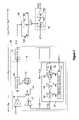
- a semiconductor device 10may include 4 semiconductor die 12 , 14 , 16 , and 18 , some of which may be identical to each other or different from each other.
- the die 12 - 18may be mounted on a surface 20 of a substrate 24 , and external terminals in the form of a ball grid array 28 may be mounted on an opposed surface 30 of the substrate 24 .
- One of the balls 32 of the ball grid array 28may receive a clock signal (CLK”), and a plurality of other balls 34 (only one is shown) may receive and transmit data signals.
- Individual balls of the array ball grid array 28may be coupled to the die 12 - 18 through respective internal balls 38 positioned against each surface of the die 12 - 18 between adjacent die or between the die 12 and the substrate 24 .
- Signalsmay be coupled from one surface of the die 12 - 18 to an opposite surface by internal electrical connectors such as through silicon vias (“tsv”) 40 .
- FIG. 2shows a semiconductor device 52 that also includes the stacked die 12 - 18 .
- the semiconductor device 52may be substantially similar to the semiconductor device 10 of FIG. 1 . Therefore, in the interest of brevity and clarity, identical reference numerals will be used to identify identical components.
- the device 52differs from the device 10 by using bond wires 62 , 64 , 66 , 68 as internal electrical connectors to couple all or some signals from the substrate 24 to the die 12 - 18 . However, the device 52 may also use the internal balls 38 to couple signals between the die 12 - 18 .
- the propagation delay in coupling signals between the external electrical connectors 28 and the die 12 - 18may differ from die-to-die.
- the CLK signalwill be received by the die 12 - 18 with increasingly larger delays from the die 12 to the die 18 .
- read datamay be output from the die 12 - 18 at increasing distances from the electrical connectors 28 .
- the propagation delay in coupling the read data from each of the die 12 - 18 to the electrical connectors 28may increase from the die 12 to the die 18 .
- the “data eye” during which the read data is validmay become increasingly later for die 12 - 18 farther away from the electrical connectors 28 . More importantly, the overlap in the respective data eyes from the die 12 - 18 may set the overall data eye for the device 12 - 18 during which read data from the devices 10 , 50 is valid regardless of which die originated the read data. The size of the data eye may therefore become smaller as the common data valid time overlaps in the respective data eyes from the die 12 - 18 become smaller. A smaller data eye may make it more difficult for an external device to correctly latch read data from the devices 10 , 50 . This skewed data eye problem gets worse when duty cycle distortion is present. Similar types of problems may exist for other types of signals, such as write data signals.
- the problems resulting from differences in the connections between the electrical connectors 28 and each of the die 12 - 18may also result in problems other than signal propagation problems, such as output slew rate skew, ZQ calibration termination impedance mismatch, etc.
- the longer signal paths between the electrical connectors 28 and the die farther away from the electrical connectors 28may increase the resistance between the electrical connectors 28 and the die 12 - 18 farther away from the electrical connectors.
- the “drive strength” of signal transmitters on the die 12 - 18may become increasing less away from the electrical connectors 28 .
- the increased resistance between the electrical connectors 28 and the die 12 - 18 farther away from the electrical connectors 28may also cause the termination impedance of the balls of aball grid array, for example, to be larger for die 12 - 18 farther away from the ball grid array.
- FIG. 1is a schematic cross-sectional view of a semiconductor device using a plurality of stacked die.
- FIG. 2is a schematic cross-sectional view of another semiconductor device using a plurality of stacked die.
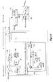
- FIG. 3is a schematic diagram showing an embodiment of a clock circuit that may provide an internal clock signal to a clock tree in a semiconductor die.
- FIG. 4is a schematic diagram showing another embodiment of a clock circuit that may provide an internal clock signal to a clock tree in a semiconductor die.
- FIG. 5is a schematic cross-sectional view of an embodiment configured to generate signals indicative of the position of a die in a stack.
- FIG. 6is a schematic diagram showing an embodiment of a compensation circuit that may be used to compensate for drive strength and termination impedance variations resulting from difference in the location of stacked semiconductor die.
- FIG. 7is a block diagram of an embodiment of a memory die including an embodiment of a clock circuit.
- a locked-loopsuch as a delay lock loop
- a clock circuit 100may use a delay lock loop (“DLL”) 110 receiving an input clock (“CLK”) signal to provide an internal clock signal (“ICLK”) to a clock tree 140 .
- DLLdelay lock loop
- the clock tree 140may distribute the ICLK signal to a variety of circuits for a variety of uses. For example, as shown in FIG.
- the ICLK signalmay be used to provide a data clock (“DCLK”) signal to an output buffer 150 .
- the output buffer 150may include a data register 154 that is clocked by the DCLK signal and/or its complementary signal to provide data signals (“Data”) to an output buffer circuit 158 to output read data (“DQ”) signals (only one is shown).
- Datadata signals
- DQread data signals
- the read DQ signalsmay be routed from each of the die 12 - 18 to the electrical connectors of a device, such as devices 10 and 52 , including the clock circuit 100 .
- the clock circuit 100may also include a duty cycle correction (DCC) circuit and output buffer 116 to ensure that the duty cycle of the ICLK signal is at substantially 50%.
- the ICLK signalmay also be coupled though a feedback path, which may include a feedback FB Model Delay Unit 120 .
- a feedback clock (“FBCLK”) signalwhich may be a delayed version of the ICLK signal, may be coupled through an input buffer (“IB”) model delay 124 to an input of a phase detector 128 .
- the phase detector 128detects a phase difference between the signals applied to its input and outputs a phase error signal indicative of the phase difference between the input signals.
- This phase error signalmay be provided to shift logic 132 that generates a control signal based on the phase error signal to adjust the delay of a DLL delay line 108 to which the CLK signal is applied.
- the delay of the delay line 108may be increased or decreased in order to synchronize the inputs of the phase detector 128 .
- the DLL 110is said to be “locked.”
- the goal of the clock circuit 100is to output the DQ signals to respective externally accessible terminals, such as respective balls of the ball grid array 28 , in synchronism with a CLK signal applied to an externally accessible terminal, such a respective ball of the ball grid array 28 .
- the signals applied to the phase detector 128will be synchronized with each other.
- the read data DQmay be output from the output buffer 150 after a delay equal to the sum of a propagation delay t TR through the clock tree 140 and a delay t OB through the output buffer circuit 150 .
- the DQ signalsmay then be output but may be delayed by a propagation delay to from one of the die 12 - 18 to the external terminals such as the ball grid array 28 .
- the DQ signalsmay be output from the semiconductor device 10 after a delay of t TR +t OB +t O from the signal that the input buffer 104 applies to the delay line 108 .
- the delay of the DQ signals being applied to the external terminals of the device 10 relative to the CLK signal applied to the external terminalsmay be further increased by the propagation delay t I of the CLK signal from the external terminals to the die 12 - 18 as well as the propagation delay t IB through the input buffer 104 .
- the functions of the IB model delay 124 and the FB Model Delay Unit 120are to compensate for these delays so the DQ signals at the external DQ terminals of the device are synchronized to the CLK signal at the external CLK terminal of the device, such as one of devices 10 or 52 .
- the IB model delay 124models the propagation delay of the input buffer 104 so that, if the signals applied to the inputs of the phase detector 128 are synchronized, the FBCLK signal will be synchronized to the CLK signal.
- the remaining delays discussed aboveare compensated for by the FB Model Delay Unit 120 .
- the DQ signalsmay be applied to the external terminals of the device in synchronism with the CLK signals applied to the external terminals of the device.
- the propagation delay t TR of the clock tree 140 and the propagation delay t OB of the output buffer 150may be substantially the same for all of the die 12 - 18
- the propagation delay t I of the CLK signal from the external DQ terminals of the device and the propagation delay t O from the die 12 - 18 to the external DQ terminals of the devicemay be different for each location of the die 12 - 18 .
- the propagation delay of the CLK signal for the die 12will be t I — 0
- the propagation delay for the die 14will be t I — 0 +t I — 1
- the propagation delay for the die 16will be t I — 0 +t I — 1 +t I — 2
- the propagation delay for the die 18will be t I — 0 +t I — 1 , +t I — 2 +t I — 3 .
- the propagation delay of the DQ signals for the die 12will be t O — 0
- the propagation delay for the die 14will be t O — 0 +t O — 1
- the propagation delay for the die 16will be t O — 0 +t O — 1 +t O — 2
- the propagation delay for the die 18will be t O — 0 +t O — 1 , +t O — 2 +t O — 3 .
- the FB Model Delay Unit 120may compensate for all of these differences in propagation delays by including a FB Model circuit 160 and a plurality of switchable delays 164 , 166 , 168 that may be selectively enabled.
- the switchable delay 164When enabled, the switchable delay 164 may provide a delay of t I — 1 + O — 1 , the switchable delay 166 may provide a delay of t I — 2 + O — 2 , and the switchable delay 168 may provide a delay of t I — 3 + O — 3 .
- the switchable delays 164 - 168may be enabled by respective select signals Sel 1 -Sel 3 from a Multi-Stack Logic Control circuit 170 , which, in turn, may receive a 4-bit Sel ⁇ 0:3> signal. Examples of techniques for generating the Sel ⁇ 0:3> signal will be provided below, it being understood that other techniques may also be used.
- the delay of the FB Model circuit 160may, for example, be equal to the sum of the propagation delay t I — 0 of the CLK signal from an external terminal of the device 10 , 52 to the die 12 , the propagation delay t O — 0 of the DQ signals from the die 12 to an external terminal of the device, the delay t TR of the clock treee 140 , and the delay t OB of the output buffer 150 .
- the Sel ⁇ 0:3> signalmay identify the location of the die 12 - 18 relative to the external electrical connector(s) of the device, such as one of devices 10 , 52 .
- the Sel ⁇ 0:3> signalmay be decoded as shown in Table A below.
- variable delay of the FB Model Delay Unit 120may therefore allow the DQ signals to be output from external terminals of the device, such as respective balls of the ball grid array 28 , in synchronism with the CLK signal being applied to an external terminal of the device, such as one of the balls of the ball grid array 28 .
- the switchable delays 14 - 18are coupled in series with each other, and their delays may be substantially equal to each other since the delay from one die 12 - 18 to the next may be substantially equal.
- the switchable delays 14 - 18 coupled in series with each othermay provide increasingly larger delays when they are enabled. In such an embodiment, if the switchable delays were not enabled, they would provide substantially no delay.
- the delay of a first switchable delaymay be t I — 1 +t O — 1
- the delay of a second switchable delaymay be t I — 1 +t O — 1 +t I — 2 +t O — 2
- the delay of a third switchable delaymay be t I — 1 +t O — 1 +t I — 2 +t O — 2 +t I — 3 +t O — 3 .
- the Sel ⁇ 0:3> signalcould be decoded as shown in Table C, below.
- the FB Model Delay Unit 120may use switchable delays coupled to each other in parallel.
- the clock circuit 200uses many of the same components that are used in the clock circuit 100 of FIG. 3 . Therefore, in the interests of brevity and clarity, corresponding components have been provided with the same references numerals, and descriptions of their functions and operation will not be repeated.
- the clock circuit 200differs from the clock circuit 100 by including a the FB Model Delay Unit 220 that uses switchable delays 224 , 226 , 228 that may be coupled in parallel with each other between the output of a FB Model 222 and a 4-input multiplexer 230 .
- the multiplexer 230may have a 4-bit control input that receives the Sel ⁇ 0:3> signal to select the output from either one of the FB Model 160 or one of the switchable delays 224 , 226 , 228 .
- the delays of the switchable delaysmay be the same delays as the switchable delays used in the series coupled switchable delays having increasingly larger delays as explained above.
- the delay of a first switchable delay 224may be t I — 1 +t O — 1
- the delay of a second switchable delay 226may be t I — 1 +t O — 1 +t I — 2 +t O — 2
- the delay of a third switchable delay 228may be t I — 1 +t O — 1 +t I — 2 +t O — 2 +t I — 3 +t O — 3 .
- the FB Model 222may also provide the same delay as the FB Model 160 used in the clock circuit 100 except that the FB Model 160 may provide an additional delay T MUX corresponding to the propagation delay through the multiplexer 230 .
- the resulting delays provided by the FB Model Delay Unit 220would therefore be the same as the delays provided by the FB Model Delay Unit 120 except for the additional delay T MUX .
- locked-loopsin the form of delay-lock loops
- phase-lock loopsmay also be used to compensate for differences in signal propagation delays in other embodiment.
- a variety of techniquesmay be used to generate the Sel ⁇ 0:3> signals to provide indications of the locations of each die 12 - 18 with respect to the external electrical connectors of a device (e.g., to provide an indication of the position of a die within a stack).
- an integrated circuit using the clock circuits 100 , 200 or a clock circuit according to some other embodimentmay include a programmable option, such as an array of antifuses, that may be programmed when a semiconductor device is packaged to designate the position of each of the die 12 - 18 .
- Other techniquesmay be used to automatically generate the Sel ⁇ 0:3> signals to indicate die position.
- a semiconductor device 300may include 4 semiconductor die 312 , 314 , 316 , and 318 that may each include a clock circuit, such as the clock circuit 100 shown in FIG. 1 or some other embodiment of a clock circuit.
- the die 312may be mounted on a substrate 324 that includes a plurality of electrical contacts, such as contacts 338 (only 5 of which are shown in FIG. 5 ).
- contacts 338only 5 of which are shown in FIG. 5 .
- Four of these contacts 338i.e., 340 , 342 , 344 , 346 may be coupled to respective contacts 350 , 352 , 354 , 356 fabricated on one surface of the die 312 .
- Each of the contacts 350 - 354may be coupled to a respective tsv 360 , 362 , 364 , which may be offset from the respective ones of the contacts 350 - 354 by respective laterally extending conductors 370 , 372 , 374 .
- the contact 356is not connected to any tsv.
- Each of the die 314 , 316 , 318may be identical to the die 312 .
- Each of the die 314 - 318may be coupled to an underlying die by a respective ball grid array.
- the number of balls 382 - 386 in each of the arrays 380 that are used to couple the contacts 350 - 356 to the tsv's 360 - 364 of the underlying die 312 - 316 , respectively,may continuously decrease from the die 312 to the die 316 .
- three balls 382 - 386may be used to couple the tsv's 360 - 364 of the die 312 to the respective contacts 352 - 356 of the die 314 , but only two balls 384 , 386 may be used to couple the tsv's 362 , 364 of the die 314 to the respective contacts 354 , 356 of the die 316 . Similarly, only one ball 386 may be used to couple the tsv 364 of the die 316 to the contact 356 of the die 318 .
- the contacts 340 - 346are biased to a first voltage, such as a supply voltage V CC , to represent a logic “1,” and a particular bias voltage, such as 0 volts, to represent a logic “0” is applied to each of the contacts 340 - 346 of the substrate 324 , the 4 voltage levels present on each of the contacts 350 - 356 may be used to provide the 4 bits of the Sel ⁇ 0:3> signal ( FIGS. 3 and 4 ).
- the Sel ⁇ 0:3> signal for the die 312will be “ 0000 ,” the Sel ⁇ 0:3> signal for the die 314 will be “ 1000 ,” the Sel ⁇ 0:3> signal for the die 316 will be “ 1100 ,” and the Sel ⁇ 0:3> signal for the die 318 will be “ 0111 .”
- the Sel ⁇ 0:3> signal identifying the location of each die 312 - 318 in the stackmay be automatically generated. However, other techniques may alternatively be used to generate the Sel ⁇ 0:3> signal.
- embodiments described abovecompensate for variations in the signal propagation time between the substrate 24 and the die 12 - 18 resulting from differences in the locations of the die in a device, such as a stacked device 10 , 52 .
- variations other than signal propagation delay variationsmay exist for different die 12 - 18 in the stack. Therefore, viewed more broadly, embodiments may compensate for these other variations resulting from differences in the locations of the die 12 - 18 .
- a signalsuch as the Sel ⁇ 0:3> signal, may provide an indication of the location of a die in the stack.
- a compensation circuitsuch as the clock circuits 100 , 200 , may receive the location indicating signal and may adjust a characteristic (e.g., of operation) of one or more circuits fabricated in the die to compensate for the location-induced variation.
- the termination impedance of an externally accessible terminal of a diemay vary with different locations of the die in a stack because of the conductor impedance may increase as signal paths extending between a die and a substrate become longer for die that are farther from the substrate.
- the “drive strength”, slew rate of an output driver, such as a data output buffermay decrease for a die that is farther from the substrate because of the greater conductor length.
- Various embodimentsmay be used to compensate for these termination impedance and/or drive strength variations.
- the circuit 400may include a plurality of PMOS pull-up transistors 402 - 410 , which may have their respective sources coupled to a first voltage, such as a supply voltage V CC or VDDQ.
- the drains of the transistors 402 - 410may be coupled to an output terminal 420 through respective resistances 422 - 430 . All or some of the resistances 422 - 430 may have the same resistance value, although they may also all be different from each other.
- the gates of the transistors 402 , 404may be coupled to receive respective active-low pull-up signals PUPEnF ⁇ 0:1> while the gates of the other transistors 406 , 408 , 410 may be coupled to an output of respective OR-gates 436 , 438 , 440 .
- the OR-gates 436 , 438 , 440may each have a first input that receives an active-low pull-up signal PUPEnF and a second input that receives a respective active-low select signal SelF ⁇ 1:3>.
- a plurality of NMOS pull-down transistors 452 - 460may have their respective sources coupled to a second voltage, such as ground.
- the drains of the transistors 452 - 460may also be coupled to the output terminal 420 through respective resistances 472 - 480 , such as discrete resistors. Again, all or some of the resistances 472 - 480 may have the same or different resistance values.
- the gates of the transistors 452 , 454may be coupled to receive respective active-high pull-down signals PDNEn ⁇ 0:1> while the gates of the other transistors 456 , 458 , 460 may be coupled to an output of respective AND-gates 466 , 468 , 470 .
- each of the AND-gates 466 , 468 , 470may have a first input that may receive an active-high pull-down signal PDNEn and a second input that may receive a respective active-high select signal Sel ⁇ 1:3>.
- one or more of the pull-up signals PUPEnF ⁇ 0:1>, PUPENF signalsmay be driven low by suitable means such as by a memory device to drive the output terminal 420 high.
- one or more of the pull-down signals PDNEn ⁇ 0:1>, PDNEN signalsmay be driven high by suitable means to drive the output terminal 420 low.
- one or both of the pull-up signals PUPEnF ⁇ 0:1>may be driven low to drive the output terminal 420 high, and one or both of the pull-down signals PDNEn ⁇ 0:1> may be driven high to drive the output terminal 420 low.
- Either the PUPEnF signal or the PDNEn signalmay also be driven low or high, respectively, but the SefF ⁇ 1:3> signals may be inactive high and the Sef ⁇ 1:3> signals are inactive low so that the respective transistors 406 - 410 or 456 - 460 are not turned ON.
- the SefF ⁇ 1> signalmay be low to enable the OR-gate 436 and the Sef ⁇ 1> signal may be high to enable the AND-gate 466 so that 3 transistors 402 - 406 are turned ON to drive the output terminal 420 high or 3 transistors 455 - 456 are turned ON to drive the output terminal 420 low.
- the SefF ⁇ 2> signalmay also be driven low (along with the SefF ⁇ 1> signal) to enable the OR-gates 436 , 438 , and the Sef ⁇ 1> and Sef ⁇ 2> signal may also be driven high to enable the AND-gates 466 , 468 .
- the SefF ⁇ 3> signalmay also be low and the Sef ⁇ 3> signal may also be high so that all 5 transistors 402 - 410 are turned ON to drive the output terminal 420 high or all 5 transistors 452 - 460 are turned ON to drive the output terminal 420 low. In this manner, die farther away from the substrate may be provided with a greater drive strength and an reduced termination impedance.
- FIG. 7illustrates an embodiment of a portion of a memory die 500 .
- An embodiment of a clock circuit 550may be included in the memory die 500 .
- the timing of an internal clock signal ICLK generated by the clock circuit 550may be adjusted as a function of the location of the die 500 in a device, such as a stacked device.
- the memory die 500may include an array 502 of memory cells, which may be, for example, DRAM memory cells, SRAM memory cells, flash memory cells, or some other types of memory cells.
- the memory die 500may include a command decoder 506 that may receive memory commands through a command bus 508 and may generate corresponding control signals within the memory die 500 to carry out various memory operations. Row and column address signals may be applied to the memory device 500 through an address bus 520 and provided to an address latch 510 . The address latch may then output a separate column address and a separate row address.
- a command decoder 506may receive memory commands through a command bus 508 and may generate corresponding control signals within the memory die 500 to carry out various memory operations.
- Row and column address signalsmay be applied to the memory device 500 through an address bus 520 and provided to an address latch 510 .
- the address latchmay then output a separate column address and a separate row address.
- the row and column addressesmay be provided by the address latch 510 to a row address decoder 522 and a column address decoder 528 , respectively.
- the column address decoder 528may select bit lines extending through the array 502 corresponding to respective column addresses.
- the row address decoder 522may be connected to word line driver 524 that may activate respective rows of memory cells in the array 502 corresponding to received row addresses.
- the selected data linee.g., a bit line or bit lines
- the clock circuit 550may provide an ICLK signal to the clock tree circuit 140 .
- the clock tree circuit 140may provide a DCLK signal for timing, for example, to clock the output buffer 534 .
- the DCLK signal output by the clock tree circuit 140can be used for timing different components as well.
- Write datamay be applied to the memory array 502 through a data input buffer 544 and the memory array read/write circuitry 530 .
- the command decoder 506may respond to memory commands applied to the command bus 508 to perform various operations on the memory array 502 . In particular, the command decoder 506 may be used to generate internal control signals to read data from and write data to the memory array 502 .
- Circuits that compensate for other location-induced variations in a characteristic (e.g., of performance) of the memory die 500may also be used in the memory die 500 .
- a characteristic of a circuit of the diemay be adjusted to compensate for a location-induced variation.
Landscapes
- Engineering & Computer Science (AREA)
- Physics & Mathematics (AREA)
- Microelectronics & Electronic Packaging (AREA)
- Computer Hardware Design (AREA)
- Nonlinear Science (AREA)
- Condensed Matter Physics & Semiconductors (AREA)
- General Physics & Mathematics (AREA)
- Power Engineering (AREA)
- Dram (AREA)
- Semiconductor Integrated Circuits (AREA)
- Design And Manufacture Of Integrated Circuits (AREA)
Abstract
Description
- Embodiments of this invention relate to devices that have a plurality of semiconductor die, and more particularly, in one or more embodiments, to stacked integrated circuit die and clock signals.
- Periodic signals are used in a variety of electronic devices. One type of periodic signal is a clock signal that can be used to establish the timing of a signal or the timing at which an operation is performed on a signal. For example, data signals are typically coupled to and from memory devices, such as synchronous dynamic random access memory (“SDRAM”) devices, in synchronism with a clock signal or data strobe signal. More specifically, read data signals are typically coupled from a memory device in synchronism with either a clock signal or a read data strobe signal that may be synchronous with a clock signal. The read data strobe signal is normally generated by the same memory device that is outputting the read data signals. Write data signals are typically latched into a memory device in synchronism with a clock signal or a write data strobe signal that may also be synchronous with a clock signal. Other signals generated in electronic devices, such as memory devices or memory controllers, are often synchronized or triggered by an internal clock signal. For example a clock signal may be used in a memory device for latching write data and/or outputting read data. The clock signal is typically generated in the memory device from an internal clock signal using a delay-lock loop.
- One of the advantages of using a delay lock loop to generate an internal clock signal in an integrated circuit is that various delays in an integrated circuit can be modeled by delay model circuits and used in the feedback path of a delay lock loop to compensate for such delays. For example, the delay in coupling a clock signal through a clock tree to a read data latch can be modeled by a model delay in the feedback path of a delay lock loop that generates the clock signal. As a result, read data may be latched and thus output from the memory device substantially in synchronism with a clock signal despite a propagation delay of a clock signal through the clock tree.
- While various techniques such as a delay lock loop containing a model delay may alleviate to some extent problems resulting from propagation delays in integrated circuits, the problems of signal propagation delays may become more severe in a semiconductor device using multiple semiconductor die, such as where the multiple die are stacked. More specifically, even if propagation delays can be compensated for in each die, there may still be propagation delays in coupling signals between each die and external electrical connectors (e.g., terminals) of the integrated circuit device. With reference to
FIG. 1 , asemiconductor device 10 may include 4 semiconductor die12,14,16, and18, some of which may be identical to each other or different from each other. The die12-18 may be mounted on asurface 20 of asubstrate 24, and external terminals in the form of aball grid array 28 may be mounted on anopposed surface 30 of thesubstrate 24. One of theballs 32 of theball grid array 28 may receive a clock signal (CLK”), and a plurality of other balls34 (only one is shown) may receive and transmit data signals. Individual balls of the arrayball grid array 28 may be coupled to the die12-18 through respectiveinternal balls 38 positioned against each surface of the die12-18 between adjacent die or between the die12 and thesubstrate 24. Signals may be coupled from one surface of the die12-18 to an opposite surface by internal electrical connectors such as through silicon vias (“tsv”)40. FIG. 2 shows asemiconductor device 52 that also includes the stacked die12-18. Thesemiconductor device 52 may be substantially similar to thesemiconductor device 10 ofFIG. 1 . Therefore, in the interest of brevity and clarity, identical reference numerals will be used to identify identical components. Thedevice 52 differs from thedevice 10 by usingbond wires substrate 24 to the die12-18. However, thedevice 52 may also use theinternal balls 38 to couple signals between the die12-18.- Regardless of whether the signal coupling technique shown in
FIG. 1 orFIG. 2 is used or some other technique is used, the propagation delay in coupling signals between the externalelectrical connectors 28 and the die12-18 may differ from die-to-die. For example, the CLK signal will be received by the die12-18 with increasingly larger delays from the die12 to thedie 18. As a result, for example, read data may be output from the die12-18 at increasing distances from theelectrical connectors 28. Moreover, the propagation delay in coupling the read data from each of the die12-18 to theelectrical connectors 28 may increase from the die12 to thedie 18. Insofar as the read data from thedevices 10,50 may be latched by an external device in synchronism with the CLK signal or some other signal, the “data eye” during which the read data is valid may become increasingly later for die12-18 farther away from theelectrical connectors 28. More importantly, the overlap in the respective data eyes from the die12-18 may set the overall data eye for the device12-18 during which read data from thedevices 10,50 is valid regardless of which die originated the read data. The size of the data eye may therefore become smaller as the common data valid time overlaps in the respective data eyes from the die12-18 become smaller. A smaller data eye may make it more difficult for an external device to correctly latch read data from thedevices 10,50. This skewed data eye problem gets worse when duty cycle distortion is present. Similar types of problems may exist for other types of signals, such as write data signals. - The problems resulting from differences in the connections between the
electrical connectors 28 and each of the die12-18 may also result in problems other than signal propagation problems, such as output slew rate skew, ZQ calibration termination impedance mismatch, etc. For example, the longer signal paths between theelectrical connectors 28 and the die farther away from theelectrical connectors 28 may increase the resistance between theelectrical connectors 28 and the die12-18 farther away from the electrical connectors. As a result, the “drive strength” of signal transmitters on the die12-18 may become increasing less away from theelectrical connectors 28. The increased resistance between theelectrical connectors 28 and the die12-18 farther away from theelectrical connectors 28 may also cause the termination impedance of the balls of aball grid array, for example, to be larger for die12-18 farther away from the ball grid array. FIG. 1 is a schematic cross-sectional view of a semiconductor device using a plurality of stacked die.FIG. 2 is a schematic cross-sectional view of another semiconductor device using a plurality of stacked die.FIG. 3 is a schematic diagram showing an embodiment of a clock circuit that may provide an internal clock signal to a clock tree in a semiconductor die.FIG. 4 is a schematic diagram showing another embodiment of a clock circuit that may provide an internal clock signal to a clock tree in a semiconductor die.FIG. 5 is a schematic cross-sectional view of an embodiment configured to generate signals indicative of the position of a die in a stack.FIG. 6 is a schematic diagram showing an embodiment of a compensation circuit that may be used to compensate for drive strength and termination impedance variations resulting from difference in the location of stacked semiconductor die.FIG. 7 is a block diagram of an embodiment of a memory die including an embodiment of a clock circuit.- A locked-loop, such as a delay lock loop, may be used to compensate for disparate signal propagation delays between external electrical connectors (e.g., terminals, contacts, etc.), such as the ball grid array28 (
FIGS. 1 and 2 ), and a plurality of die. As shown inFIG. 3 , aclock circuit 100 may use a delay lock loop (“DLL”)110 receiving an input clock (“CLK”) signal to provide an internal clock signal (“ICLK”) to aclock tree 140. When enabled by an active CkEn signal, theclock tree 140 may distribute the ICLK signal to a variety of circuits for a variety of uses. For example, as shown inFIG. 3 , the ICLK signal may be used to provide a data clock (“DCLK”) signal to anoutput buffer 150. Theoutput buffer 150 may include adata register 154 that is clocked by the DCLK signal and/or its complementary signal to provide data signals (“Data”) to anoutput buffer circuit 158 to output read data (“DQ”) signals (only one is shown). As explained above with reference toFIGS. 1 and 2 , the read DQ signals may be routed from each of the die12-18 to the electrical connectors of a device, such asdevices clock circuit 100. - The
clock circuit 100 may also include a duty cycle correction (DCC) circuit andoutput buffer 116 to ensure that the duty cycle of the ICLK signal is at substantially 50%. The ICLK signal may also be coupled though a feedback path, which may include a feedback FB Model Delay Unit120. A feedback clock (“FBCLK”) signal, which may be a delayed version of the ICLK signal, may be coupled through an input buffer (“IB”)model delay 124 to an input of aphase detector 128. Thephase detector 128 detects a phase difference between the signals applied to its input and outputs a phase error signal indicative of the phase difference between the input signals. This phase error signal may be provided to shiftlogic 132 that generates a control signal based on the phase error signal to adjust the delay of aDLL delay line 108 to which the CLK signal is applied. The delay of thedelay line 108 may be increased or decreased in order to synchronize the inputs of thephase detector 128. When synchronized, theDLL 110 is said to be “locked.” - The goal of the
clock circuit 100 is to output the DQ signals to respective externally accessible terminals, such as respective balls of theball grid array 28, in synchronism with a CLK signal applied to an externally accessible terminal, such a respective ball of theball grid array 28. As mentioned above, when theDLL 110 is locked, the signals applied to thephase detector 128 will be synchronized with each other. However, the read data DQ may be output from theoutput buffer 150 after a delay equal to the sum of a propagation delay tTRthrough theclock tree 140 and a delay tOBthrough theoutput buffer circuit 150. The DQ signals may then be output but may be delayed by a propagation delay to from one of the die12-18 to the external terminals such as theball grid array 28. Thus, the DQ signals may be output from thesemiconductor device 10 after a delay of tTR+tOB+tOfrom the signal that theinput buffer 104 applies to thedelay line 108. The delay of the DQ signals being applied to the external terminals of thedevice 10 relative to the CLK signal applied to the external terminals may be further increased by the propagation delay tIof the CLK signal from the external terminals to the die12-18 as well as the propagation delay tIBthrough theinput buffer 104. The functions of theIB model delay 124 and the FBModel Delay Unit 120 are to compensate for these delays so the DQ signals at the external DQ terminals of the device are synchronized to the CLK signal at the external CLK terminal of the device, such as one ofdevices IB model delay 124 models the propagation delay of theinput buffer 104 so that, if the signals applied to the inputs of thephase detector 128 are synchronized, the FBCLK signal will be synchronized to the CLK signal. The remaining delays discussed above are compensated for by the FBModel Delay Unit 120. Specifically, if the delay of the FB Model Delay is equal to tTR+tOB+tO+tIand the FBCLK signal is synchronized to the CLK signal at the input of thebuffer 104, the ICLK signal will lag the CLK signal by tXL=N*tCK−(tTR+tOB+tO+tI), where N is the DLL total clock loop number. As a result, the DQ signals may be applied to the external terminals of the device in synchronism with the CLK signals applied to the external terminals of the device. - Unfortunately, while the propagation delay tTRof the
clock tree 140 and the propagation delay tOBof theoutput buffer 150 may be substantially the same for all of the die12-18, the propagation delay tIof the CLK signal from the external DQ terminals of the device and the propagation delay tOfrom the die12-18 to the external DQ terminals of the device may be different for each location of the die12-18. Specifically, the propagation delay of the CLK signal for the die12 will be tI— 0, the propagation delay for the die14 will be tI— 0+tI— 1, the propagation delay for the die16 will be tI— 0+tI— 1+tI— 2, and the propagation delay for the die18 will be tI— 0+tI— 1, +tI— 2+tI— 3. The propagation delay of the DQ signals for the die12 will be tO— 0, the propagation delay for the die14 will be tO— 0+tO— 1, the propagation delay for the die16 will be tO— 0+tO— 1+tO— 2, and the propagation delay for the die18 will be tO— 0+tO— 1, +tO— 2+tO— 3. The FBModel Delay Unit 120 may compensate for all of these differences in propagation delays by including aFB Model circuit 160 and a plurality ofswitchable delays switchable delay 164 may provide a delay of tI— 1+O— 1, theswitchable delay 166 may provide a delay of tI— 2+O— 2, and theswitchable delay 168 may provide a delay of tI— 3+O— 3. The switchable delays164-168 may be enabled by respective select signals Sel1-Sel 3 from a Multi-StackLogic Control circuit 170, which, in turn, may receive a 4-bit Sel<0:3> signal. Examples of techniques for generating the Sel<0:3> signal will be provided below, it being understood that other techniques may also be used. - The delay of the
FB Model circuit 160 may, for example, be equal to the sum of the propagation delay tI— 0of the CLK signal from an external terminal of thedevice die 12, the propagation delay tO— 0of the DQ signals from the die12 to an external terminal of the device, the delay tTRof theclock treee 140, and the delay tOBof theoutput buffer 150. - In operation, the Sel<0:3> signal may identify the location of the die12-18 relative to the external electrical connector(s) of the device, such as one of
devices TABLE A STACK POSITION Sel<0:3> Sel1 Sel2 Sel3 0 000 0 0 0 1 100 1 0 0 2 010 1 1 0 3 001 1 1 1 - As shown in Table A, none of the switchable delays are enabled for the die12 in
stack position 0, only theswitchable delay 164 is enabled for the die14 instack position 1, bothswitchable delays stack position 2, and all of the switchable delays164-168 are enabled for the die18 instack position 3. As a result, the delays provided by the FBModel Delay Unit 120 are as shown in Table B, below. TABLE B DIE DELAY 12 tTR+ tOB+ tI — 0+ tO— 014 tTR+ tOB+ tI — 0+ tI— 1+ tO— 0+ tO— 116 tTR+ tOB+ tI — 0+ tI— 1+ tI— 2+ tO— 0+ tO— 1+tO— 218 tTR+ tOB+ tI — 0+ tI— 1+ tI— 2+ tI— 3. + tO— 0+ tO— 1+ tO— 2+tO — 3- The variable delay of the FB
Model Delay Unit 120 may therefore allow the DQ signals to be output from external terminals of the device, such as respective balls of theball grid array 28, in synchronism with the CLK signal being applied to an external terminal of the device, such as one of the balls of theball grid array 28. - In the embodiment of the
clock circuit 100 shown inFIG. 3 , the switchable delays14-18 are coupled in series with each other, and their delays may be substantially equal to each other since the delay from one die12-18 to the next may be substantially equal. In another embodiment, the switchable delays14-18 coupled in series with each other may provide increasingly larger delays when they are enabled. In such an embodiment, if the switchable delays were not enabled, they would provide substantially no delay. Therefore, the delay of a first switchable delay may be tI— 1+tO— 1, the delay of a second switchable delay may be tI— 1+tO— 1+tI— 2+tO— 2, and the delay of a third switchable delay may be tI— 1+tO— 1+tI— 2+tO— 2+tI— 3+tO— 3. For this embodiment, the Sel<0:3> signal could be decoded as shown in Table C, below. TABLE C STACK POSITION Sel<0:3> Sel1 Sel2 Sel3 0 000 0 0 0 1 100 1 0 0 2 010 0 1 0 3 001 0 0 1 - The resulting delays provided by the FB Model Delay would therefore be the same as shown in Table B.
- Although the previously described embodiments of the FB
Model Delay Unit 120 use switchable delays that may be coupled in series with each other, in another embodiment of a clock circuit200 shown inFIG. 4 the FBModel Delay Unit 120 may use switchable delays coupled to each other in parallel. The clock circuit200 uses many of the same components that are used in theclock circuit 100 ofFIG. 3 . Therefore, in the interests of brevity and clarity, corresponding components have been provided with the same references numerals, and descriptions of their functions and operation will not be repeated. The clock circuit200 differs from theclock circuit 100 by including a the FB Model Delay Unit220 that usesswitchable delays FB Model 222 and a 4-input multiplexer 230. Themultiplexer 230 may have a 4-bit control input that receives the Sel<0:3> signal to select the output from either one of theFB Model 160 or one of theswitchable delays switchable delay 224 may be tI— 1+tO— 1, the delay of a secondswitchable delay 226 may be tI— 1+tO— 1+tI— 2+tO— 2, and the delay of a thirdswitchable delay 228 may be tI— 1+tO— 1+tI— 2+tO— 2+tI— 3+tO— 3. - The
FB Model 222 may also provide the same delay as theFB Model 160 used in theclock circuit 100 except that theFB Model 160 may provide an additional delay TMUXcorresponding to the propagation delay through themultiplexer 230. The resulting delays provided by the FB Model Delay Unit220 would therefore be the same as the delays provided by the FBModel Delay Unit 120 except for the additional delay TMUX. - Although the foregoing describes specific embodiments of locked-loops in the form of delay-lock loops, other types of locked-loops, such as phase-lock loops, may also be used to compensate for differences in signal propagation delays in other embodiment.
- A variety of techniques may be used to generate the Sel<0:3> signals to provide indications of the locations of each die12-18 with respect to the external electrical connectors of a device (e.g., to provide an indication of the position of a die within a stack). For example, an integrated circuit using the
clock circuits 100,200 or a clock circuit according to some other embodiment may include a programmable option, such as an array of antifuses, that may be programmed when a semiconductor device is packaged to designate the position of each of the die12-18. Other techniques may be used to automatically generate the Sel<0:3> signals to indicate die position. - For example, another technique that may be used to generate the Sel<0:3> signals is shown in
FIG. 5 . As shown inFIG. 5 , asemiconductor device 300 may include 4 semiconductor die312,314,316, and318 that may each include a clock circuit, such as theclock circuit 100 shown inFIG. 1 or some other embodiment of a clock circuit. Thedie 312 may be mounted on asubstrate 324 that includes a plurality of electrical contacts, such as contacts338 (only 5 of which are shown inFIG. 5 ). Four of these contacts338, i.e.,340,342,344,346 may be coupled torespective contacts die 312. Each of the contacts350-354 may be coupled to arespective tsv conductors contact 356 is not connected to any tsv. - Each of the
die die 312. Each of the die314-318 may be coupled to an underlying die by a respective ball grid array. However, the number of balls382-386 in each of thearrays 380 that are used to couple the contacts350-356 to the tsv's360-364 of the underlying die312-316, respectively, may continuously decrease from thedie 312 to thedie 316. Thus, three balls382-386 may be used to couple the tsv's360-364 of the die312 to the respective contacts352-356 of thedie 314, but only twoballs respective contacts die 316. Similarly, only oneball 386 may be used to couple thetsv 364 of the die316 to thecontact 356 of thedie 318. As a result, all 4 contacts350-356 of thedie 312 are coupled to the contacts340-346 of thesubstrate 324, only 3 contacts352-356 of thedie 314 are coupled to the contacts342-346, only 2contacts die 316 are coupled to the contacts342-346, and only 1contact 356 of thedie 318 is coupled to the contacts342-346. If the contacts340-346 are biased to a first voltage, such as a supply voltage VCC, to represent a logic “1,” and a particular bias voltage, such as 0 volts, to represent a logic “0” is applied to each of the contacts340-346 of thesubstrate 324, the 4 voltage levels present on each of the contacts350-356 may be used to provide the 4 bits of the Sel<0:3> signal (FIGS. 3 and 4 ). In such case the Sel<0:3> signal for thedie 312 will be “0000,” the Sel<0:3> signal for thedie 314 will be “1000,” the Sel<0:3> signal for thedie 316 will be “1100,” and the Sel<0:3> signal for thedie 318 will be “0111.” Thus, the Sel<0:3> signal identifying the location of each die312-318 in the stack may be automatically generated. However, other techniques may alternatively be used to generate the Sel<0:3> signal. - The embodiments described above compensate for variations in the signal propagation time between the
substrate 24 and the die12-18 resulting from differences in the locations of the die in a device, such as astacked device clock circuits 100,200, may receive the location indicating signal and may adjust a characteristic (e.g., of operation) of one or more circuits fabricated in the die to compensate for the location-induced variation. For example, the termination impedance of an externally accessible terminal of a die may vary with different locations of the die in a stack because of the conductor impedance may increase as signal paths extending between a die and a substrate become longer for die that are farther from the substrate. Similarly, the “drive strength”, slew rate of an output driver, such as a data output buffer, may decrease for a die that is farther from the substrate because of the greater conductor length. Various embodiments may be used to compensate for these termination impedance and/or drive strength variations. - One embodiment of a
compensation circuit 400 that may compensate for both termination impedance and drive strength variations resulting from differences in die location is shown inFIG. 6 . Thecircuit 400 may include a plurality of PMOS pull-up transistors402-410, which may have their respective sources coupled to a first voltage, such as a supply voltage VCCor VDDQ. The drains of the transistors402-410 may be coupled to anoutput terminal 420 through respective resistances422-430. All or some of the resistances422-430 may have the same resistance value, although they may also all be different from each other. The gates of thetransistors other transistors gates gates - In a similar manner, a plurality of NMOS pull-down transistors452-460 may have their respective sources coupled to a second voltage, such as ground. The drains of the transistors452-460 may also be coupled to the
output terminal 420 through respective resistances472-480, such as discrete resistors. Again, all or some of the resistances472-480 may have the same or different resistance values. The gates of thetransistors other transistors gates gates gates - In operation, one or more of the pull-up signals PUPEnF<0:1>, PUPENF signals may be driven low by suitable means such as by a memory device to drive the
output terminal 420 high. Alternatively, one or more of the pull-down signals PDNEn<0:1>, PDNEN signals may be driven high by suitable means to drive theoutput terminal 420 low. The number of transistors404-410 or452-460 that are turned ON by the pull-up signals or pull-down signals, respectively, determine both the termination impedance and the drive strength of the transistors. If thecompensation circuit 400 is on the die closest to the substrate, i.e., die #0, one or both of the pull-up signals PUPEnF<0:1> may be driven low to drive theoutput terminal 420 high, and one or both of the pull-down signals PDNEn<0:1> may be driven high to drive theoutput terminal 420 low. Either the PUPEnF signal or the PDNEn signal may also be driven low or high, respectively, but the SefF<1:3> signals may be inactive high and the Sef<1:3> signals are inactive low so that the respective transistors406-410 or456-460 are not turned ON. One the other hand, if thecompensation circuit 400 is ondie # 1, the SefF<1> signal may be low to enable the OR-gate436 and the Sef<1> signal may be high to enable the AND-gate466 so that 3 transistors402-406 are turned ON to drive theoutput terminal 420 high or 3 transistors455-456 are turned ON to drive theoutput terminal 420 low. Similarly, if thecompensation circuit 400 is ondie # 2, the SefF<2> signal may also be driven low (along with the SefF<1> signal) to enable the OR-gates gates output terminal 420 high or 4 transistors452-458 may be turned ON to drive theoutput terminal 420 low. Finally, if thecompensation circuit 400 is ondie # 3, the SefF<3> signal may also be low and the Sef<3> signal may also be high so that all 5 transistors402-410 are turned ON to drive theoutput terminal 420 high or all 5 transistors452-460 are turned ON to drive theoutput terminal 420 low. In this manner, die farther away from the substrate may be provided with a greater drive strength and an reduced termination impedance. - The compensation circuits according to various embodiments may be used in connection with a wide variety of semiconductor devices. For example,
FIG. 7 illustrates an embodiment of a portion of amemory die 500. An embodiment of a clock circuit550 may be included in the memory die500. As with theclock circuits 100,200, the timing of an internal clock signal ICLK generated by the clock circuit550 may be adjusted as a function of the location of the die500 in a device, such as a stacked device. The memory die500 may include anarray 502 of memory cells, which may be, for example, DRAM memory cells, SRAM memory cells, flash memory cells, or some other types of memory cells. The memory die500 may include acommand decoder 506 that may receive memory commands through acommand bus 508 and may generate corresponding control signals within the memory die500 to carry out various memory operations. Row and column address signals may be applied to thememory device 500 through anaddress bus 520 and provided to anaddress latch 510. The address latch may then output a separate column address and a separate row address. - The row and column addresses may be provided by the
address latch 510 to arow address decoder 522 and acolumn address decoder 528, respectively. Thecolumn address decoder 528 may select bit lines extending through thearray 502 corresponding to respective column addresses. Therow address decoder 522 may be connected toword line driver 524 that may activate respective rows of memory cells in thearray 502 corresponding to received row addresses. The selected data line (e.g., a bit line or bit lines) corresponding to a received column address may be coupled to read/write circuitry 530 to provide read data to a data output buffer534 via an input-output data bus 540. The clock circuit550 may provide an ICLK signal to theclock tree circuit 140. In response to the ICLK signal, theclock tree circuit 140 may provide a DCLK signal for timing, for example, to clock the output buffer534. Although not specifically shown inFIG. 7 , the DCLK signal output by theclock tree circuit 140 can be used for timing different components as well. Write data may be applied to thememory array 502 through adata input buffer 544 and the memory array read/write circuitry 530. Thecommand decoder 506 may respond to memory commands applied to thecommand bus 508 to perform various operations on thememory array 502. In particular, thecommand decoder 506 may be used to generate internal control signals to read data from and write data to thememory array 502. Circuits that compensate for other location-induced variations in a characteristic (e.g., of performance) of the memory die500, such as its termination impedance and/or drive strength, may also be used in the memory die500. For example, such circuit may providing an indication of the location of each of a plurality of semiconductor die. In response to the indication, a characteristic of a circuit of the die may be adjusted to compensate for a location-induced variation. Although specific embodiments have been disclosed, persons skilled in the art will recognize that changes may be made in form and detail without departing from the invention. Such modifications are well within the skill of those ordinarily skilled in the art. Accordingly, the invention is not limited except as by the appended claims.
Claims (28)
Priority Applications (7)
| Application Number | Priority Date | Filing Date | Title |
|---|---|---|---|
| US12/548,883US9160349B2 (en) | 2009-08-27 | 2009-08-27 | Die location compensation |
| KR1020127006055AKR101443463B1 (en) | 2009-08-27 | 2010-08-02 | Die location compensation |
| PCT/US2010/044123WO2011028348A2 (en) | 2009-08-27 | 2010-08-02 | Die location compensation |
| EP10814131.8AEP2471180B1 (en) | 2009-08-27 | 2010-08-02 | Die location compensation |
| CN201080037704.6ACN102484477B (en) | 2009-08-27 | 2010-08-02 | Die Position Compensation |
| TW099128113ATWI459722B (en) | 2009-08-27 | 2010-08-23 | Die location compensation |
| US14/843,676US10063241B2 (en) | 2009-08-27 | 2015-09-02 | Die location compensation |
Applications Claiming Priority (1)
| Application Number | Priority Date | Filing Date | Title |
|---|---|---|---|
| US12/548,883US9160349B2 (en) | 2009-08-27 | 2009-08-27 | Die location compensation |
Related Child Applications (1)
| Application Number | Title | Priority Date | Filing Date |
|---|---|---|---|
| US14/843,676ContinuationUS10063241B2 (en) | 2009-08-27 | 2015-09-02 | Die location compensation |
Publications (2)
| Publication Number | Publication Date |
|---|---|
| US20110050303A1true US20110050303A1 (en) | 2011-03-03 |
| US9160349B2 US9160349B2 (en) | 2015-10-13 |
Family
ID=43623926
Family Applications (2)
| Application Number | Title | Priority Date | Filing Date |
|---|---|---|---|
| US12/548,883Active2032-01-13US9160349B2 (en) | 2009-08-27 | 2009-08-27 | Die location compensation |
| US14/843,676ActiveUS10063241B2 (en) | 2009-08-27 | 2015-09-02 | Die location compensation |
Family Applications After (1)
| Application Number | Title | Priority Date | Filing Date |
|---|---|---|---|
| US14/843,676ActiveUS10063241B2 (en) | 2009-08-27 | 2015-09-02 | Die location compensation |
Country Status (6)
| Country | Link |
|---|---|
| US (2) | US9160349B2 (en) |
| EP (1) | EP2471180B1 (en) |
| KR (1) | KR101443463B1 (en) |
| CN (1) | CN102484477B (en) |
| TW (1) | TWI459722B (en) |
| WO (1) | WO2011028348A2 (en) |
Cited By (14)
| Publication number | Priority date | Publication date | Assignee | Title |
|---|---|---|---|---|
| US20110103162A1 (en)* | 2009-10-30 | 2011-05-05 | Hynix Semiconductor Inc. | Semiconductor memory apparatus |
| US20110102011A1 (en)* | 2009-09-28 | 2011-05-05 | Imec | Method and device for testing tsvs in a 3d chip stack |
| US20110267099A1 (en)* | 2010-04-28 | 2011-11-03 | Elpida Memory, Inc. | Semiconductor device generating complementary output signals |
| US20120176192A1 (en)* | 2005-08-30 | 2012-07-12 | Micron Technology, Inc. | Self-Identifying Stacked Die Semiconductor Components |
| US20140027771A1 (en)* | 2012-07-26 | 2014-01-30 | Yasuo Satoh | Device identification assignment and total device number detection |
| US8816736B2 (en)* | 2010-04-09 | 2014-08-26 | Micron Technology, Inc. | Clock signal generators having a reduced power feedback clock path and methods for generating clocks |
| US8947141B2 (en) | 2010-10-06 | 2015-02-03 | Micron Technology, Inc. | Differential amplifiers, clock generator circuits, delay lines and methods |
| US9246496B2 (en)* | 2014-05-19 | 2016-01-26 | SK Hynix Inc. | Semiconductor device, semiconductor system and method for operating semiconductor device |
| US9361985B2 (en) | 2013-01-02 | 2016-06-07 | Samsung Electronics Co., Ltd. | Nonvolatile memory devices including simultaneous impedance calibration and input command |
| US20160172017A1 (en)* | 2014-12-11 | 2016-06-16 | Micron Technology, Inc. | Tracking and correction of timing signals |
| US10063241B2 (en) | 2009-08-27 | 2018-08-28 | Micron Technology, Inc. | Die location compensation |
| US20190181869A1 (en)* | 2017-12-08 | 2019-06-13 | Samsung Electronics Co, Ltd | Memory device including a delay locked loop and operating method of the memory device |
| US20230063347A1 (en)* | 2021-08-30 | 2023-03-02 | Micron Technology, Inc. | Tuned datapath in stacked memory device |
| US20250088193A1 (en)* | 2023-09-13 | 2025-03-13 | Advanced Micro Devices, Inc. | Systems and methods for driver calibration in die-to-die interfaces |
Families Citing this family (9)
| Publication number | Priority date | Publication date | Assignee | Title |
|---|---|---|---|---|
| US8787060B2 (en) | 2010-11-03 | 2014-07-22 | Netlist, Inc. | Method and apparatus for optimizing driver load in a memory package |
| US8587340B2 (en) | 2012-03-27 | 2013-11-19 | Micron Technology, Inc. | Apparatuses including scalable drivers and methods |
| US9417685B2 (en)* | 2013-01-07 | 2016-08-16 | Micron Technology, Inc. | Power management |
| KR20150138703A (en)* | 2014-06-02 | 2015-12-10 | 에스케이하이닉스 주식회사 | Stack package |
| KR102373543B1 (en)* | 2015-04-08 | 2022-03-11 | 삼성전자주식회사 | Method and device for controlling operation using temperature deviation in multi-chip package |
| US10600770B2 (en) | 2018-05-14 | 2020-03-24 | Micron Technology, Inc. | Semiconductor dice assemblies, packages and systems, and methods of operation |
| US10530367B2 (en)* | 2018-12-28 | 2020-01-07 | Intel Corporation | Clock synchronization in multi-die field programmable gate array devices |
| US10803962B1 (en)* | 2019-04-01 | 2020-10-13 | Micron Technology, Inc. | Current monitoring in semiconductor packages |
| US20250199068A1 (en)* | 2023-12-15 | 2025-06-19 | Advanced Micro Devices, Inc. | Apparatus, system, and method for distributing die-specific signals across die stacks |
Citations (25)
| Publication number | Priority date | Publication date | Assignee | Title |
|---|---|---|---|---|
| US5122679A (en)* | 1988-10-14 | 1992-06-16 | Hitachi, Ltd. | Integrated logic circuit with clock skew adjusters |
| US5565816A (en)* | 1995-08-18 | 1996-10-15 | International Business Machines Corporation | Clock distribution network |
| US5570054A (en)* | 1994-09-26 | 1996-10-29 | Hitachi Micro Systems, Inc. | Method and apparatus for adaptive clock deskewing |
| US5670903A (en)* | 1994-08-30 | 1997-09-23 | Nec Corporation | Clock signal distribution circuit having a small clock skew |
| US5751665A (en)* | 1995-07-14 | 1998-05-12 | Oki Electric Industry Co., Ltd. | Clock distributing circuit |
| US5852640A (en)* | 1995-06-26 | 1998-12-22 | Kliza; Phillip S. | Clock distribution apparatus with current sensed skew cancelling |
| US5949262A (en)* | 1998-01-07 | 1999-09-07 | International Business Machines Corporation | Method and apparatus for coupled phase locked loops |
| US6323714B1 (en)* | 2000-02-03 | 2001-11-27 | Hewlett-Packard Company | System and method for deskewing synchronous clocks in a very large scale integrated circuit |
| US6448661B1 (en)* | 2001-02-09 | 2002-09-10 | Samsung Electornics Co., Ltd. | Three-dimensional multi-chip package having chip selection pads and manufacturing method thereof |
| US20030071669A1 (en)* | 2001-10-11 | 2003-04-17 | Dean Liu | Deskewing global clock skew using localized DLLs |
| US20030137335A1 (en)* | 2001-03-09 | 2003-07-24 | Joseph Hofstra | Reduced jitter clock generator circuit and method for applying properly phased clock signals to clocked devices |
| US20040041604A1 (en)* | 2002-09-03 | 2004-03-04 | Kizer Jade M. | Phase jumping locked loop circuit |
| US6744287B2 (en)* | 1999-11-23 | 2004-06-01 | Intel Corporation | Slew rate control circuit |
| US6791175B2 (en)* | 2001-09-29 | 2004-09-14 | Kabushiki Kaisha Toshiba | Stacked type semiconductor device |
| US20050231247A1 (en)* | 2004-04-20 | 2005-10-20 | Hynix Semiconductor Inc. | Delay locked loop |
| US6996026B2 (en)* | 2003-04-30 | 2006-02-07 | Infineon Technologies Ag | Devices for synchronizing clock signals |
| US7015741B2 (en)* | 2003-12-23 | 2006-03-21 | Intel Corporation | Adaptive body bias for clock skew compensation |
| US20060267212A1 (en)* | 2005-05-09 | 2006-11-30 | Elpida Memory, Inc. | Semiconductor device |
| US7161400B2 (en)* | 2003-08-04 | 2007-01-09 | Rambus Inc. | Phase synchronization for wide area integrated circuits |
| US20080043548A1 (en)* | 2006-06-23 | 2008-02-21 | Won-Chang Jung | Semiconductor memory device for stack package and read data skew control method thereof |
| US20080204091A1 (en)* | 2007-02-28 | 2008-08-28 | Samsung Electronics Co., Ltd. | Semiconductor chip package and method for fabricating semiconductor chip |
| US20080258700A1 (en)* | 2007-04-18 | 2008-10-23 | Lsi Logic Corporation | Method and apparatus for adjusting on-chip delay with power supply control |
| US20090154285A1 (en)* | 2007-12-14 | 2009-06-18 | Mosaid Technologies Incorporated | Memory controller with flexible data alignment to clock |
| US7729197B2 (en)* | 2002-05-16 | 2010-06-01 | Micron Technology, Inc. | Memory device having a delay locked loop with frequency control |
| US7971088B2 (en)* | 2007-02-27 | 2011-06-28 | Samsung Electronics Co., Ltd. | Clock skew controller and integrated circuit including the same |
Family Cites Families (17)
| Publication number | Priority date | Publication date | Assignee | Title |
|---|---|---|---|---|
| CA1301261C (en)* | 1988-04-27 | 1992-05-19 | Wayne D. Grover | Method and apparatus for clock distribution and for distributed clock synchronization |
| US5442776A (en)* | 1994-06-30 | 1995-08-15 | International Business Machines, Corp. | Electronically tuneable computer clocking system and method of electronically tuning distribution lines of a computer clocking system |
| US5696951A (en)* | 1996-01-03 | 1997-12-09 | Credence Systems Corporation | Signal deskewing system for synchronous logic circuit |
| US6124744A (en)* | 1996-03-26 | 2000-09-26 | Kabushiki Kaisha Toshiba | Electronic circuit apparatus having circuits for effectively compensating for clock skew |
| US6150866A (en)* | 1997-04-01 | 2000-11-21 | Fujitsu Limited | Clock supplying circuit and integrated circuit device using it |
| US5867448A (en)* | 1997-06-11 | 1999-02-02 | Cypress Semiconductor Corp. | Buffer for memory modules with trace delay compensation |
| US6191632B1 (en)* | 1998-07-24 | 2001-02-20 | Matsushita Electric Industrial Co., Ltd. | Clock generation circuit and semiconductor integrated circuit |
| JP3515708B2 (en)* | 1999-05-17 | 2004-04-05 | 日本電気株式会社 | Semiconductor storage device |
| KR100513806B1 (en)* | 2000-12-30 | 2005-09-13 | 주식회사 하이닉스반도체 | Semiconductor Device |
| US6605969B2 (en) | 2001-10-09 | 2003-08-12 | Micron Technology, Inc. | Method and circuit for adjusting the timing of ouput data based on an operational mode of output drivers |
| US6952123B2 (en)* | 2002-03-22 | 2005-10-04 | Rambus Inc. | System with dual rail regulated locked loop |
| US7180165B2 (en)* | 2003-09-05 | 2007-02-20 | Sanmina, Sci Corporation | Stackable electronic assembly |
| KR100546135B1 (en)* | 2004-05-17 | 2006-01-24 | 주식회사 하이닉스반도체 | Memory device with delay lock loop |
| US7726197B2 (en) | 2006-04-26 | 2010-06-01 | Honeywell International Inc. | Force sensor package and method of forming same |
| KR100917630B1 (en)* | 2008-04-30 | 2009-09-17 | 주식회사 하이닉스반도체 | Delay lock loop circuit |
| US8289806B2 (en)* | 2008-06-27 | 2012-10-16 | Micron Technology, Inc. | Multiple device apparatus, systems, and methods |
| US9160349B2 (en) | 2009-08-27 | 2015-10-13 | Micron Technology, Inc. | Die location compensation |
- 2009
- 2009-08-27USUS12/548,883patent/US9160349B2/enactiveActive
- 2010
- 2010-08-02WOPCT/US2010/044123patent/WO2011028348A2/enactiveApplication Filing
- 2010-08-02EPEP10814131.8Apatent/EP2471180B1/enactiveActive
- 2010-08-02KRKR1020127006055Apatent/KR101443463B1/enactiveActive
- 2010-08-02CNCN201080037704.6Apatent/CN102484477B/enactiveActive
- 2010-08-23TWTW099128113Apatent/TWI459722B/enactive
- 2015
- 2015-09-02USUS14/843,676patent/US10063241B2/enactiveActive
Patent Citations (26)
| Publication number | Priority date | Publication date | Assignee | Title |
|---|---|---|---|---|
| US5122679A (en)* | 1988-10-14 | 1992-06-16 | Hitachi, Ltd. | Integrated logic circuit with clock skew adjusters |
| US5670903A (en)* | 1994-08-30 | 1997-09-23 | Nec Corporation | Clock signal distribution circuit having a small clock skew |
| US5570054A (en)* | 1994-09-26 | 1996-10-29 | Hitachi Micro Systems, Inc. | Method and apparatus for adaptive clock deskewing |
| US5852640A (en)* | 1995-06-26 | 1998-12-22 | Kliza; Phillip S. | Clock distribution apparatus with current sensed skew cancelling |
| US5751665A (en)* | 1995-07-14 | 1998-05-12 | Oki Electric Industry Co., Ltd. | Clock distributing circuit |
| US5565816A (en)* | 1995-08-18 | 1996-10-15 | International Business Machines Corporation | Clock distribution network |
| US5949262A (en)* | 1998-01-07 | 1999-09-07 | International Business Machines Corporation | Method and apparatus for coupled phase locked loops |
| US6744287B2 (en)* | 1999-11-23 | 2004-06-01 | Intel Corporation | Slew rate control circuit |
| US6323714B1 (en)* | 2000-02-03 | 2001-11-27 | Hewlett-Packard Company | System and method for deskewing synchronous clocks in a very large scale integrated circuit |
| US6448661B1 (en)* | 2001-02-09 | 2002-09-10 | Samsung Electornics Co., Ltd. | Three-dimensional multi-chip package having chip selection pads and manufacturing method thereof |
| US20030137335A1 (en)* | 2001-03-09 | 2003-07-24 | Joseph Hofstra | Reduced jitter clock generator circuit and method for applying properly phased clock signals to clocked devices |
| US6791175B2 (en)* | 2001-09-29 | 2004-09-14 | Kabushiki Kaisha Toshiba | Stacked type semiconductor device |
| US6991964B2 (en)* | 2001-09-29 | 2006-01-31 | Kabushiki Kaisha Toshiba | Stacked type semiconductor device |
| US20030071669A1 (en)* | 2001-10-11 | 2003-04-17 | Dean Liu | Deskewing global clock skew using localized DLLs |
| US7729197B2 (en)* | 2002-05-16 | 2010-06-01 | Micron Technology, Inc. | Memory device having a delay locked loop with frequency control |
| US20040041604A1 (en)* | 2002-09-03 | 2004-03-04 | Kizer Jade M. | Phase jumping locked loop circuit |
| US6996026B2 (en)* | 2003-04-30 | 2006-02-07 | Infineon Technologies Ag | Devices for synchronizing clock signals |
| US7161400B2 (en)* | 2003-08-04 | 2007-01-09 | Rambus Inc. | Phase synchronization for wide area integrated circuits |
| US7015741B2 (en)* | 2003-12-23 | 2006-03-21 | Intel Corporation | Adaptive body bias for clock skew compensation |
| US20050231247A1 (en)* | 2004-04-20 | 2005-10-20 | Hynix Semiconductor Inc. | Delay locked loop |
| US20060267212A1 (en)* | 2005-05-09 | 2006-11-30 | Elpida Memory, Inc. | Semiconductor device |
| US20080043548A1 (en)* | 2006-06-23 | 2008-02-21 | Won-Chang Jung | Semiconductor memory device for stack package and read data skew control method thereof |
| US7971088B2 (en)* | 2007-02-27 | 2011-06-28 | Samsung Electronics Co., Ltd. | Clock skew controller and integrated circuit including the same |
| US20080204091A1 (en)* | 2007-02-28 | 2008-08-28 | Samsung Electronics Co., Ltd. | Semiconductor chip package and method for fabricating semiconductor chip |
| US20080258700A1 (en)* | 2007-04-18 | 2008-10-23 | Lsi Logic Corporation | Method and apparatus for adjusting on-chip delay with power supply control |
| US20090154285A1 (en)* | 2007-12-14 | 2009-06-18 | Mosaid Technologies Incorporated | Memory controller with flexible data alignment to clock |
Cited By (25)
| Publication number | Priority date | Publication date | Assignee | Title |
|---|---|---|---|---|
| US20120176192A1 (en)* | 2005-08-30 | 2012-07-12 | Micron Technology, Inc. | Self-Identifying Stacked Die Semiconductor Components |
| US8472232B2 (en)* | 2005-08-30 | 2013-06-25 | Micron Technology, Inc. | Self-identifying stacked die semiconductor components |
| US10063241B2 (en) | 2009-08-27 | 2018-08-28 | Micron Technology, Inc. | Die location compensation |
| US8593170B2 (en)* | 2009-09-28 | 2013-11-26 | Imec | Method and device for testing TSVS in a 3D chip stack |
| US20110102011A1 (en)* | 2009-09-28 | 2011-05-05 | Imec | Method and device for testing tsvs in a 3d chip stack |
| US20110103162A1 (en)* | 2009-10-30 | 2011-05-05 | Hynix Semiconductor Inc. | Semiconductor memory apparatus |
| US8816736B2 (en)* | 2010-04-09 | 2014-08-26 | Micron Technology, Inc. | Clock signal generators having a reduced power feedback clock path and methods for generating clocks |
| US8384433B2 (en)* | 2010-04-28 | 2013-02-26 | Elpida Memory, Inc. | Semiconductor device generating complementary output signals |
| US20110267099A1 (en)* | 2010-04-28 | 2011-11-03 | Elpida Memory, Inc. | Semiconductor device generating complementary output signals |
| US8947141B2 (en) | 2010-10-06 | 2015-02-03 | Micron Technology, Inc. | Differential amplifiers, clock generator circuits, delay lines and methods |
| US20140027771A1 (en)* | 2012-07-26 | 2014-01-30 | Yasuo Satoh | Device identification assignment and total device number detection |
| US9478502B2 (en)* | 2012-07-26 | 2016-10-25 | Micron Technology, Inc. | Device identification assignment and total device number detection |
| US9361985B2 (en) | 2013-01-02 | 2016-06-07 | Samsung Electronics Co., Ltd. | Nonvolatile memory devices including simultaneous impedance calibration and input command |
| US9246496B2 (en)* | 2014-05-19 | 2016-01-26 | SK Hynix Inc. | Semiconductor device, semiconductor system and method for operating semiconductor device |
| US20160172017A1 (en)* | 2014-12-11 | 2016-06-16 | Micron Technology, Inc. | Tracking and correction of timing signals |
| US9842633B2 (en)* | 2014-12-11 | 2017-12-12 | Micron Technology, Inc. | Tracking and correction of timing signals |
| US10692550B2 (en) | 2014-12-11 | 2020-06-23 | Micron Technology, Inc. | Tracking and correction of timing signals |
| US20190181869A1 (en)* | 2017-12-08 | 2019-06-13 | Samsung Electronics Co, Ltd | Memory device including a delay locked loop and operating method of the memory device |
| CN109903794A (en)* | 2017-12-08 | 2019-06-18 | 三星电子株式会社 | Memory device including delay locked loop and method of operating the memory device |
| US10491223B2 (en)* | 2017-12-08 | 2019-11-26 | Samsung Electronics Co., Ltd. | Memory device including a delay locked loop and operating method of the memory device |
| US20230063347A1 (en)* | 2021-08-30 | 2023-03-02 | Micron Technology, Inc. | Tuned datapath in stacked memory device |
| WO2023033906A1 (en)* | 2021-08-30 | 2023-03-09 | Micron Technology, Inc | Tuned datapath in stacked memory device |
| US12008236B2 (en)* | 2021-08-30 | 2024-06-11 | Micron Technology, Inc. | Tuned datapath in stacked memory device |
| US20240319879A1 (en)* | 2021-08-30 | 2024-09-26 | Micron Technology, Inc. | Tuned datapath in stacked memory device |
| US20250088193A1 (en)* | 2023-09-13 | 2025-03-13 | Advanced Micro Devices, Inc. | Systems and methods for driver calibration in die-to-die interfaces |
Also Published As
| Publication number | Publication date |
|---|---|
| CN102484477B (en) | 2015-06-24 |
| US10063241B2 (en) | 2018-08-28 |
| US9160349B2 (en) | 2015-10-13 |
| TWI459722B (en) | 2014-11-01 |
| KR101443463B1 (en) | 2014-09-23 |
| US20150381189A1 (en) | 2015-12-31 |
| CN102484477A (en) | 2012-05-30 |
| KR20120056268A (en) | 2012-06-01 |
| TW201130230A (en) | 2011-09-01 |
| EP2471180B1 (en) | 2020-10-07 |
| EP2471180A2 (en) | 2012-07-04 |
| WO2011028348A2 (en) | 2011-03-10 |
| WO2011028348A3 (en) | 2011-04-28 |
| EP2471180A4 (en) | 2013-08-28 |
Similar Documents
| Publication | Publication Date | Title |
|---|---|---|
| US9160349B2 (en) | Die location compensation | |
| USRE50511E1 (en) | Memory devices, systems and methods employing command/address calibration | |
| US10832787B2 (en) | Methods for memory interface calibration | |
| US9378783B2 (en) | I/O circuit with phase mixer for slew rate control | |
| US9397661B2 (en) | On-die termination circuit and on-die termination method | |
| US9036435B2 (en) | Semiconductor apparatus, method for delaying signal thereof, stacked semiconductor memory apparatus, and method for generating signal thereof | |
| US20070070733A1 (en) | Circuit and method for outputting aligned strobe signal and parallel data signal | |
| US10241538B2 (en) | Resynchronization of a clock associated with each data bit in a double data rate memory system |
Legal Events
| Date | Code | Title | Description |
|---|---|---|---|
| AS | Assignment | Owner name:MICRON TECHNOLOGY, INC., IDAHO Free format text:ASSIGNMENT OF ASSIGNORS INTEREST;ASSIGNOR:MA, YANTAO;REEL/FRAME:023157/0599 Effective date:20090821 | |
| FEPP | Fee payment procedure | Free format text:PAYOR NUMBER ASSIGNED (ORIGINAL EVENT CODE: ASPN); ENTITY STATUS OF PATENT OWNER: LARGE ENTITY | |
| STCF | Information on status: patent grant | Free format text:PATENTED CASE | |
| CC | Certificate of correction | ||
| AS | Assignment | Owner name:U.S. BANK NATIONAL ASSOCIATION, AS COLLATERAL AGENT, CALIFORNIA Free format text:SECURITY INTEREST;ASSIGNOR:MICRON TECHNOLOGY, INC.;REEL/FRAME:038669/0001 Effective date:20160426 Owner name:U.S. BANK NATIONAL ASSOCIATION, AS COLLATERAL AGEN Free format text:SECURITY INTEREST;ASSIGNOR:MICRON TECHNOLOGY, INC.;REEL/FRAME:038669/0001 Effective date:20160426 | |
| AS | Assignment | Owner name:MORGAN STANLEY SENIOR FUNDING, INC., AS COLLATERAL AGENT, MARYLAND Free format text:PATENT SECURITY AGREEMENT;ASSIGNOR:MICRON TECHNOLOGY, INC.;REEL/FRAME:038954/0001 Effective date:20160426 Owner name:MORGAN STANLEY SENIOR FUNDING, INC., AS COLLATERAL Free format text:PATENT SECURITY AGREEMENT;ASSIGNOR:MICRON TECHNOLOGY, INC.;REEL/FRAME:038954/0001 Effective date:20160426 | |
| AS | Assignment | Owner name:U.S. BANK NATIONAL ASSOCIATION, AS COLLATERAL AGENT, CALIFORNIA Free format text:CORRECTIVE ASSIGNMENT TO CORRECT THE REPLACE ERRONEOUSLY FILED PATENT #7358718 WITH THE CORRECT PATENT #7358178 PREVIOUSLY RECORDED ON REEL 038669 FRAME 0001. ASSIGNOR(S) HEREBY CONFIRMS THE SECURITY INTEREST;ASSIGNOR:MICRON TECHNOLOGY, INC.;REEL/FRAME:043079/0001 Effective date:20160426 Owner name:U.S. BANK NATIONAL ASSOCIATION, AS COLLATERAL AGEN Free format text:CORRECTIVE ASSIGNMENT TO CORRECT THE REPLACE ERRONEOUSLY FILED PATENT #7358718 WITH THE CORRECT PATENT #7358178 PREVIOUSLY RECORDED ON REEL 038669 FRAME 0001. ASSIGNOR(S) HEREBY CONFIRMS THE SECURITY INTEREST;ASSIGNOR:MICRON TECHNOLOGY, INC.;REEL/FRAME:043079/0001 Effective date:20160426 | |
| AS | Assignment | Owner name:JPMORGAN CHASE BANK, N.A., AS COLLATERAL AGENT, ILLINOIS Free format text:SECURITY INTEREST;ASSIGNORS:MICRON TECHNOLOGY, INC.;MICRON SEMICONDUCTOR PRODUCTS, INC.;REEL/FRAME:047540/0001 Effective date:20180703 Owner name:JPMORGAN CHASE BANK, N.A., AS COLLATERAL AGENT, IL Free format text:SECURITY INTEREST;ASSIGNORS:MICRON TECHNOLOGY, INC.;MICRON SEMICONDUCTOR PRODUCTS, INC.;REEL/FRAME:047540/0001 Effective date:20180703 | |
| AS | Assignment | Owner name:MICRON TECHNOLOGY, INC., IDAHO Free format text:RELEASE BY SECURED PARTY;ASSIGNOR:U.S. BANK NATIONAL ASSOCIATION, AS COLLATERAL AGENT;REEL/FRAME:047243/0001 Effective date:20180629 | |
| MAFP | Maintenance fee payment | Free format text:PAYMENT OF MAINTENANCE FEE, 4TH YEAR, LARGE ENTITY (ORIGINAL EVENT CODE: M1551); ENTITY STATUS OF PATENT OWNER: LARGE ENTITY Year of fee payment:4 | |
| AS | Assignment | Owner name:MICRON TECHNOLOGY, INC., IDAHO Free format text:RELEASE BY SECURED PARTY;ASSIGNOR:MORGAN STANLEY SENIOR FUNDING, INC., AS COLLATERAL AGENT;REEL/FRAME:050937/0001 Effective date:20190731 | |
| AS | Assignment | Owner name:MICRON TECHNOLOGY, INC., IDAHO Free format text:RELEASE BY SECURED PARTY;ASSIGNOR:JPMORGAN CHASE BANK, N.A., AS COLLATERAL AGENT;REEL/FRAME:051028/0001 Effective date:20190731 Owner name:MICRON SEMICONDUCTOR PRODUCTS, INC., IDAHO Free format text:RELEASE BY SECURED PARTY;ASSIGNOR:JPMORGAN CHASE BANK, N.A., AS COLLATERAL AGENT;REEL/FRAME:051028/0001 Effective date:20190731 | |
| MAFP | Maintenance fee payment | Free format text:PAYMENT OF MAINTENANCE FEE, 8TH YEAR, LARGE ENTITY (ORIGINAL EVENT CODE: M1552); ENTITY STATUS OF PATENT OWNER: LARGE ENTITY Year of fee payment:8 |