US20110049460A1 - Single mask adder phase change memory element - Google Patents
Single mask adder phase change memory elementDownload PDFInfo
- Publication number
- US20110049460A1 US20110049460A1US12/549,997US54999709AUS2011049460A1US 20110049460 A1US20110049460 A1US 20110049460A1US 54999709 AUS54999709 AUS 54999709AUS 2011049460 A1US2011049460 A1US 2011049460A1
- Authority
- US
- United States
- Prior art keywords
- phase change
- change material
- opening
- metal region
- dielectric layer
- Prior art date
- Legal status (The legal status is an assumption and is not a legal conclusion. Google has not performed a legal analysis and makes no representation as to the accuracy of the status listed.)
- Granted
Links
- 230000008859changeEffects0.000titleclaimsabstractdescription52
- 230000015654memoryEffects0.000titleclaimsabstractdescription50
- 229910052751metalInorganic materials0.000claimsabstractdescription56
- 239000002184metalSubstances0.000claimsabstractdescription56
- 239000012782phase change materialSubstances0.000claimsabstractdescription51
- 239000004065semiconductorSubstances0.000claimsabstractdescription43
- 238000000151depositionMethods0.000claimsabstractdescription20
- 238000004519manufacturing processMethods0.000claimsabstractdescription12
- 238000005530etchingMethods0.000claimsabstractdescription5
- 238000000034methodMethods0.000claimsdescription41
- 239000007772electrode materialSubstances0.000claimsdescription15
- NRTOMJZYCJJWKI-UHFFFAOYSA-NTitanium nitrideChemical compound[Ti]#NNRTOMJZYCJJWKI-UHFFFAOYSA-N0.000claimsdescription11
- 239000000758substrateSubstances0.000claimsdescription11
- 239000000463materialSubstances0.000claimsdescription10
- WFKWXMTUELFFGS-UHFFFAOYSA-NtungstenChemical compound[W]WFKWXMTUELFFGS-UHFFFAOYSA-N0.000claimsdescription7
- 229910052721tungstenInorganic materials0.000claimsdescription7
- 239000010937tungstenSubstances0.000claimsdescription7
- 238000010586diagramMethods0.000description31
- 230000008569processEffects0.000description18
- 239000005380borophosphosilicate glassSubstances0.000description10
- 230000008021depositionEffects0.000description10
- VYPSYNLAJGMNEJ-UHFFFAOYSA-NSilicium dioxideChemical compoundO=[Si]=OVYPSYNLAJGMNEJ-UHFFFAOYSA-N0.000description8
- 230000015572biosynthetic processEffects0.000description7
- 229910052581Si3N4Inorganic materials0.000description6
- HQVNEWCFYHHQES-UHFFFAOYSA-Nsilicon nitrideChemical compoundN12[Si]34N5[Si]62N3[Si]51N64HQVNEWCFYHHQES-UHFFFAOYSA-N0.000description6
- 238000005229chemical vapour depositionMethods0.000description4
- 239000010949copperSubstances0.000description4
- 238000005516engineering processMethods0.000description4
- 229910052738indiumInorganic materials0.000description4
- 238000002955isolationMethods0.000description4
- 230000000873masking effectEffects0.000description4
- 239000011669seleniumSubstances0.000description4
- 239000000377silicon dioxideSubstances0.000description4
- 238000001020plasma etchingMethods0.000description3
- 238000005498polishingMethods0.000description3
- 239000000126substanceSubstances0.000description3
- RYGMFSIKBFXOCR-UHFFFAOYSA-NCopperChemical compound[Cu]RYGMFSIKBFXOCR-UHFFFAOYSA-N0.000description2
- 229910000618GeSbTeInorganic materials0.000description2
- 229910052802copperInorganic materials0.000description2
- 230000006870functionEffects0.000description2
- 238000001465metallisationMethods0.000description2
- 238000012986modificationMethods0.000description2
- 230000004048modificationEffects0.000description2
- 238000005240physical vapour depositionMethods0.000description2
- 235000012239silicon dioxideNutrition0.000description2
- 125000006850spacer groupChemical group0.000description2
- 229910052714telluriumInorganic materials0.000description2
- 229910000807Ga alloyInorganic materials0.000description1
- BUGBHKTXTAQXES-UHFFFAOYSA-NSeleniumChemical compound[Se]BUGBHKTXTAQXES-UHFFFAOYSA-N0.000description1
- 229910000577Silicon-germaniumInorganic materials0.000description1
- BQCADISMDOOEFD-UHFFFAOYSA-NSilverChemical compound[Ag]BQCADISMDOOEFD-UHFFFAOYSA-N0.000description1
- NINIDFKCEFEMDL-UHFFFAOYSA-NSulfurChemical compound[S]NINIDFKCEFEMDL-UHFFFAOYSA-N0.000description1
- RTAQQCXQSZGOHL-UHFFFAOYSA-NTitaniumChemical compound[Ti]RTAQQCXQSZGOHL-UHFFFAOYSA-N0.000description1
- 229910045601alloyInorganic materials0.000description1
- 239000000956alloySubstances0.000description1
- 229910052782aluminiumInorganic materials0.000description1
- XAGFODPZIPBFFR-UHFFFAOYSA-NaluminiumChemical compound[Al]XAGFODPZIPBFFR-UHFFFAOYSA-N0.000description1
- -1aluminum (Al)Chemical class0.000description1
- 230000000295complement effectEffects0.000description1
- 239000004020conductorSubstances0.000description1
- 230000009977dual effectEffects0.000description1
- APFVFJFRJDLVQX-UHFFFAOYSA-Nindium atomChemical compound[In]APFVFJFRJDLVQX-UHFFFAOYSA-N0.000description1
- 150000002500ionsChemical class0.000description1
- 238000001459lithographyMethods0.000description1
- 229910044991metal oxideInorganic materials0.000description1
- 150000004706metal oxidesChemical class0.000description1
- 150000002739metalsChemical class0.000description1
- 239000000203mixtureSubstances0.000description1
- 238000007747platingMethods0.000description1
- 229910052711seleniumInorganic materials0.000description1
- 229910052709silverInorganic materials0.000description1
- 239000004332silverSubstances0.000description1
- 238000004544sputter depositionMethods0.000description1
- 229910052717sulfurInorganic materials0.000description1
- 239000011593sulfurSubstances0.000description1
- 239000010936titaniumSubstances0.000description1
- 229910052719titaniumInorganic materials0.000description1
- 238000007704wet chemistry methodMethods0.000description1
Images


Classifications
- H—ELECTRICITY
- H10—SEMICONDUCTOR DEVICES; ELECTRIC SOLID-STATE DEVICES NOT OTHERWISE PROVIDED FOR
- H10N—ELECTRIC SOLID-STATE DEVICES NOT OTHERWISE PROVIDED FOR
- H10N70/00—Solid-state devices having no potential barriers, and specially adapted for rectifying, amplifying, oscillating or switching
- H10N70/801—Constructional details of multistable switching devices
- H10N70/881—Switching materials
- H10N70/884—Switching materials based on at least one element of group IIIA, IVA or VA, e.g. elemental or compound semiconductors
- H—ELECTRICITY
- H10—SEMICONDUCTOR DEVICES; ELECTRIC SOLID-STATE DEVICES NOT OTHERWISE PROVIDED FOR
- H10B—ELECTRONIC MEMORY DEVICES
- H10B63/00—Resistance change memory devices, e.g. resistive RAM [ReRAM] devices
- H10B63/30—Resistance change memory devices, e.g. resistive RAM [ReRAM] devices comprising selection components having three or more electrodes, e.g. transistors
- H—ELECTRICITY
- H10—SEMICONDUCTOR DEVICES; ELECTRIC SOLID-STATE DEVICES NOT OTHERWISE PROVIDED FOR
- H10N—ELECTRIC SOLID-STATE DEVICES NOT OTHERWISE PROVIDED FOR
- H10N70/00—Solid-state devices having no potential barriers, and specially adapted for rectifying, amplifying, oscillating or switching
- H10N70/011—Manufacture or treatment of multistable switching devices
- H10N70/061—Shaping switching materials
- H10N70/066—Shaping switching materials by filling of openings, e.g. damascene method
- H—ELECTRICITY
- H10—SEMICONDUCTOR DEVICES; ELECTRIC SOLID-STATE DEVICES NOT OTHERWISE PROVIDED FOR
- H10N—ELECTRIC SOLID-STATE DEVICES NOT OTHERWISE PROVIDED FOR
- H10N70/00—Solid-state devices having no potential barriers, and specially adapted for rectifying, amplifying, oscillating or switching
- H10N70/20—Multistable switching devices, e.g. memristors
- H10N70/231—Multistable switching devices, e.g. memristors based on solid-state phase change, e.g. between amorphous and crystalline phases, Ovshinsky effect
- H—ELECTRICITY
- H10—SEMICONDUCTOR DEVICES; ELECTRIC SOLID-STATE DEVICES NOT OTHERWISE PROVIDED FOR
- H10N—ELECTRIC SOLID-STATE DEVICES NOT OTHERWISE PROVIDED FOR
- H10N70/00—Solid-state devices having no potential barriers, and specially adapted for rectifying, amplifying, oscillating or switching
- H10N70/801—Constructional details of multistable switching devices
- H10N70/821—Device geometry
- H10N70/826—Device geometry adapted for essentially vertical current flow, e.g. sandwich or pillar type devices
- H—ELECTRICITY
- H10—SEMICONDUCTOR DEVICES; ELECTRIC SOLID-STATE DEVICES NOT OTHERWISE PROVIDED FOR
- H10N—ELECTRIC SOLID-STATE DEVICES NOT OTHERWISE PROVIDED FOR
- H10N70/00—Solid-state devices having no potential barriers, and specially adapted for rectifying, amplifying, oscillating or switching
- H10N70/801—Constructional details of multistable switching devices
- H10N70/881—Switching materials
- H10N70/882—Compounds of sulfur, selenium or tellurium, e.g. chalcogenides
- H10N70/8825—Selenides, e.g. GeSe
- H—ELECTRICITY
- H10—SEMICONDUCTOR DEVICES; ELECTRIC SOLID-STATE DEVICES NOT OTHERWISE PROVIDED FOR
- H10N—ELECTRIC SOLID-STATE DEVICES NOT OTHERWISE PROVIDED FOR
- H10N70/00—Solid-state devices having no potential barriers, and specially adapted for rectifying, amplifying, oscillating or switching
- H10N70/801—Constructional details of multistable switching devices
- H10N70/881—Switching materials
- H10N70/882—Compounds of sulfur, selenium or tellurium, e.g. chalcogenides
- H10N70/8828—Tellurides, e.g. GeSbTe
Definitions
- the present inventionrelates generally to semiconductor structures, and more specifically, to a semiconductor structure having an embedded single mask adder phase change memory element.
- phase change memoriestypically require some aspect of the structure to have a feature size which is sub-lithographically defined in order to maintain a small cell size for the phase change memory element and access circuitry.
- Some applications, such as fuse devices,have less stringent area requirements. In these applications, it is important to minimize the additional processing costs required to fabricate an embedded memory element into an existing complementary metal oxide semiconductor (CMOS) technology, for example.
- CMOScomplementary metal oxide semiconductor
- FIG. 1illustrates a typical semiconductor structure.
- a CMOS structure 10includes a substrate 11 having a borophosphosilicate glass (BPSG) dielectric layer 12 formed thereon.
- a plurality of conductive contacts 14(e.g., tungsten) are formed in the BPSG dielectric layer 12 and surrounded by a liner 15 of titanium nitride, for example, used prior to the deposition of the tungsten fill, to form the conductive contacts 14 .
- An access transistorhaving a gate 16 and spacers 17 adjacent to the sidewalls of the gate 16 , and source/drain regions 18 is also provided. Shallow trench isolation (STI) regions 19 are formed within the substrate 11 to provide electrical isolation between the access transistor and other devices.
- STIShallow trench isolation
- the conductive contacts 14connect to the source/drain regions 18 .
- a first metal region 19 (M 1 )is formed on top of each conductive contact 14 within a first dielectric layer 20 and capped with a first cap layer 21 .
- a second dielectric layer 23is then formed to contain vias 24 and capped with a second cap layer 25 .
- a second metal region 26 (M 2 )is formed within a third dielectric layer 28 , over each via 24 with the vias 24 connecting the first metal regions 19 to the second metal regions 26 .
- the present inventionprovides a manner in which to minimize the above-mentioned processing costs by minimizing the number of additional lithographic masking levels used within the semiconductor structure. Therefore, the present invention provides a method for fabricating an embedded phase change memory element into a semiconductor structure with the addition of only a single lithography masking operation utilizing the scaled dimensions of the semiconductor structure.
- a method of fabricating a phase change memory element within a semiconductor structureincludes etching an opening to an upper surface of a bottom electrode, the opening being formed of a height equal to a height of a metal region at a same layer within the semiconductor structure, depositing phase change material within the opening, recessing the phase change material within the opening, and forming a top electrode on the recessed phase change material.
- a method for fabricating a semiconductor structure having a single mask adder phase change memory element embedded thereinincludes recessing a plurality of conductive contacts to form a plurality of vias at an upper surface of each conductive contact within a substrate including access circuitry to be connected with the conductive contacts and first dielectric layer formed thereon, and forming a bottom electrode in each via formed; forming a first metal region within a second dielectric layer formed on a respective bottom electrode.
- the methodfurther includes etching an opening within the second dielectric layer to an upper surface of a respective bottom electrode adjacent to the first metal region, depositing phase change material within the opening; recessing the phase change material in the opening, forming a top electrode on the recessed phase change material, and forming a second metal region and a via in between the first and the second metal regions to connect the first metal region to the second metal region.
- a phase change memory element of a semiconductor structureincludes a bottom electrode formed at a contact surface of a conductive contact within a substrate having access circuitry, and an opening formed at an upper surface of the bottom electrode, the opening being formed of a height equal to a height of a metal region formed at a same layer within the semiconductor structure, and filled with phase change material and top electrode material to form the top electrode within the opening.
- a semiconductor structure having a single mask adder phase change memory element embedded thereinincludes a plurality of conductive contacts recessed to form a plurality of vias at an upper surface of each conductive contact within a substrate including access circuitry to be connected with the conductive contacts and having a first dielectric layer formed thereon, a bottom electrode formed in each via, and a first metal region formed within a second dielectric layer above the first dielectric layer at a respective bottom electrode.
- the semiconductor structurefurther includes an opening formed within the second dielectric layer to an upper surface of a respective bottom electrode and having recessed phase change memory formed therein, a top electrode formed on the recessed phase change material within the opening, a via formed in a third dielectric layer formed above the second dielectric layer, and a second metal region formed in a fourth dielectric layer above the third dielectric layer, the via is formed in between the first and the second metal regions to connect the first metal region to the second metal region.
- FIG. 1is a diagram illustrating a conventional semiconductor structure.
- FIG. 2is a diagram illustrating a fabrication operation of a semiconductor structure having an embedded phase change memory element that can be implemented within embodiments of the present invention.
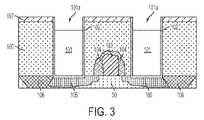
- FIG. 3is a diagram illustrating a recess operation of conductive contacts within the phase change memory element that can be implemented within embodiments of the present invention.
- FIG. 4is a diagram illustrating a deposition operation for forming a bottom electrode within the phase change memory element that can be implemented within embodiments of the present invention.
- FIG. 5is a diagram illustrating planarizing operation of the bottom electrode within the phase change memory element that can be implemented within embodiments of the present invention.
- FIG. 6is a diagram illustrating forming of a first metal region of the semiconductor structure that can be implemented within embodiments of the present invention.
- FIG. 7is a diagram illustrating the deposition of a cap layer on the first metal region that can be implemented within embodiments of the present invention.
- FIG. 8is a diagram illustrating the formation of an opening to define a bit line within the phase change memory element that can be implemented within embodiments of the present invention.
- FIG. 9is a diagram illustrating deposition of phase change material within the opening of the phase change memory element that can be implemented within embodiments of the present invention.
- FIG. 10is a diagram illustrating a planarization operation of the phase change material of the phase change memory element that can be implemented within embodiments of the present invention.
- FIG. 11is a diagram illustrating a recess operation of the phase change material that can be implemented within embodiments of the present invention.
- FIG. 12is a diagram illustrating a formation operation of a top electrode of the phase change memory element that can be implemented within embodiments of the present invention.
- FIG. 13is a diagram illustrating a planarizing operation of the top electrode of the phase change memory element that can be implemented within embodiments of the present invention.
- FIG. 14is a diagram illustrating a deposition a cap layer above the phase change memory element that can be implemented within embodiments of the present invention.
- FIG. 15is a diagram illustrating a final fabrication operation of the semiconductor structure that can be implemented within embodiments of the present invention.
- the present inventionprovides a single mask adder phase change memory element to be included in advanced CMOS technologies, bi-CMOS technologies and SiGe-based technologies.
- the fabrication of the semiconductor structure 200 (depicted in FIG. 15 ) including an embedded phase change memory element 150will now be described below with reference to FIGS. 2 through 15 .
- a diagram illustrating a fabrication operation of a phase change memory element that can be implemented within embodiments of the present inventionis provided.
- a substrate 50 having a first dielectric layer 100e.g., a borophosphosilicate glass (BPSG) dielectric layer
- BPSGborophosphosilicate glass
- the present inventionis not limited to a BPSG type wafer and any suitable type of wafer may be utilized for the purpose set forth herein.
- a plurality of conductive contacts 101are formed in the BPSG dielectric layer 100 and surrounded by a liner 102 of titanium nitride, for example, used prior to the deposition of the contact fill, to form the conductive contacts 101 .
- the conductive contacts 101may include tungsten (W), or titanium nitride (TiN), or copper (Cu), for example.
- the conductive contactsare connected to access circuitry (e.g., an access transistor) within the substrate 50 .
- the access transistorincludes a gate 103 and spacers 104 adjacent to the sidewalls of the gate 103 , and source/drain regions 105 .
- Shallow trench isolation (STI) regions 106are formed within the substrate 50 to provide electrical isolation between the access transistor and other devices.
- the conductive contacts 101connect to the source/drain regions 105 .
- a first cap layer 107is formed over the BPSG dielectric layer 100 of a predetermined thickness ranging from approximately 20 nanometers (nm) to approximately 50 nanometers (nm).
- the first cap layer 107may include silicon nitride (SiN) or silicon dioxide (SiO 2 ), for example, however the present invention is not limited hereto.
- the first cap layer 107is incorporated as a top layer of the BPSG dielectric layer 100 or alternatively the first cap layer 107 may be formed on top of the BPSG dielectric layer 100 and polished via a conventional polishing procedure. Fabrication processes of a bottom electrode will now be described below with reference to FIGS. 3 through 6 below.
- the bottom electrodemay be formed in accordance with a Patent Application entitled “FLAT LOWER BOTTOM ELECTRODE OF PHASE CHANGE MEMORY” written by Breitwisch et al. and filed on Aug. 28, 2009, which is incorporated herein by reference.
- FIG. 3is a diagram illustrating a recess operation of conductive contacts within the phase change memory element that can be implemented within embodiments of the present invention.
- the conductive contacts 101are recessed with respect to the first cap layer 107 using a reactive ion etching (RIE) process, for example, to form vias 101 a.
- RIEreactive ion etching
- the conductive contacts 101are etched a depth of the first cap layer 107 plus an additional 10-15 (nm) nanometers to form the vias 101 a.
- FIG. 4is a diagram illustrating a deposition of electrode material within the phase change memory element that can be implemented within embodiments of the present invention.
- a selectable electrode material 108is deposited on the first cap layer 107 and within the vias 101 a.
- the selectable electrode material 108may include titanium nitride (TiN), tungsten (W), or any suitable conductive material.
- TiNtitanium nitride
- Wtungsten
- any suitable conductive materialAs to one embodiment, approximately 10 nanometers (nm) of ion metal plasma (IMP) titanium may be deposited followed by a layer of titanium nitride, which is deposited via a chemical vapor deposition (CVD) process.
- the electrode material 108is compatible with the selected phase change material 118 as discussed later with reference to FIG. 9 .
- FIG. 5is a diagram illustrating a planarization operation of the electrode material within the phase change memory element that can be implemented within embodiments of the present invention.
- the electrode material 108is planarized using a chemical mechanical polishing (CMP) process, to form a lower bottom electrode 109 over each conductive contact 101 .
- CMPchemical mechanical polishing
- the first cap layer 107acts as a CMP stop layer.
- FIG. 6is a diagram illustrating formation of a first metal region within the semiconductor structure that can be implemented within embodiments of the present invention.
- a second dielectric layer 111is formed on the first cap layer 107 and a first metal region 112 (M 1 ) is formed within the second dielectric layer 111 .
- the second dielectric layer 111may be formed of silicon dioxide (SiO 2 ), for example.
- the first metal region 112may be formed of copper (Cu), for example however the present invention is not limited hereto, other types of metals including aluminum (Al), titanium nitride (TiN), and tungsten (W) based materials may be used.
- FIG. 7is a diagram illustrating the formation of a second cap layer within the semiconductor structure that can be implemented within embodiments of the present invention.
- a second cap layer 114is formed on the second dielectric layer 111 and used to cap the metal contained in the first metal region 112 .
- the second cap layer 114may be formed of the same material as the first cap layer 107 .
- both the first and second cap layers 107 and 114may be formed of silicon nitride (SiN), for example.
- SiNsilicon nitride
- FIG. 8is a diagram illustrating the formation of an opening for the phase change memory element that can be implemented within embodiments of the present invention.
- an opening 116is etched through the second cap layer 114 and the second dielectric layer 111 to contact an upper surface of the respective bottom electrode 109 .
- the opening 116may be a trench or a via.
- the opening 116is adjacent to the first metal region 112 and is formed at a height of a same height as that of the first metal region 112 .
- the opening 116is formed within the same layer (e.g., second dielectric layer 111 ) of the semiconductor structure.
- the opening 116is etched to define a bitline of the phase change memory.
- FIG. 9is a diagram illustrating a deposition of phase change material within the phase change memory element that can be implemented within embodiments of the present invention. As shown in FIG. 9 , phase change material 118 is deposited within the opening 116 , thereby filling the opening 116 and along the second cap layer 114 .
- the phase change material 118may be made of germanium-antimony-telluride (GeSbTe) or one of alloys of gallium (Ga)/Sb, indium (In)/Sb, In/selenium (Se), Sb/Te, Ge/Te, In/Sb/Te, Ga/Se/Te, Sn/Sb/Te, In/Sb/Ge, silver (Ag)/In/Sb/Te, Ge/Sb/Se/Te, Te/Ge/Sb/sulfur (S).
- GaSb/Sbgermanium-antimony-telluride
- alloysof gallium (Ga)/Sb, indium (In)/Sb, In/selenium (Se), Sb/Te, Ge/Te, In/Sb/Te, Ga/Se/Te, Sn/Sb/Te, In/Sb/Ge, silver (Ag)/In/Sb/Te,
- the phase change material 118may be deposited using a physical vapor deposition (PVD) process, a chemical vapor deposition (CVD) process, a spin-on process, or an electro-chemical plating process, for example, or any other suitable deposition operation.
- PVDphysical vapor deposition
- CVDchemical vapor deposition
- spin-on processspin-on process
- electro-chemical plating processelectro-chemical plating process
- FIG. 10is a diagram illustrating a planarizing operation of the phase change material of the phase change memory element that can be implemented within embodiments of the present invention.
- the phase change material 118is polished using a chemical mechanical polishing (CMP) process.
- CMPchemical mechanical polishing
- the phase change material 118is stopped at the second cap layer 114 .
- the second cap layer 114acts as a CMP stop layer.
- FIG. 11is a diagram illustrating a recess operation of the phase change material within the phase change memory element that can be implemented within embodiments of the present invention.
- the phase change material 118is recessed using a RIE process, a sputtering process, or a wet chemistry process, for example to form a via 120 .
- the phase change material 118is recessed such that the recessed phase change material 118 is greater than approximately 5 nanometers (nm), and preferably greater than approximately 20 nanometers (nm).
- the preferred thickness of the phase change material 118ranges from approximately 20 nanometers (nm) to 100 nanometers (nm).
- the via 120may be of a height equal to one-half a height of the first metal region 112 . According to another embodiment of the present invention, the via 120 is of a predetermined height ranging from approximately 20 nanometers (nm) to 100 nanometers (nm).
- FIG. 12is a diagram illustrating the formation of a top electrode of the phase change memory element that can be implemented within embodiments of the present invention. As shown in FIG. 12 , a top electrode 122 (as depicted in FIG. 13 ) is formed by first depositing electrode material 121 (e.g., a phase change material capping layer) such as titanium nitride (TiN) for example, on the second cap layer 114 and within the via 120 .
- first depositing electrode material 121e.g., a phase change material capping layer
- TiNtitanium nitride
- FIG. 13is a diagram illustrating a planarization operation of the top electrode 122 of the phase change memory.
- the material 121is removed from the upper surface of the second cap layer 114 such that the material 121 (e.g., the CMP titanium nitride (TN)) stops at the second cap layer 114 to form the top electrode 122 .
- the bottom electrode 109 and the top electrode 122are made of the same material.
- a resulting phase change memory element 150is formed.
- the phase change material 118 and the top electrode 122 togetherare of a same height as the first metal region 112 within the semiconductor structure.
- FIG. 14is a diagram illustrating deposition of a third cap layer within the semiconductor structure that can be implemented within embodiments of the present invention.
- a third cap layer 124is formed on an upper surface of the second cap layer 114 and the top electrode 122 to cap the top electrode 122 .
- the third cap layer 124may be formed of the same material as that of the first and second cap layers 107 and 114 .
- all three cap layers 107 , 114 and 124may be formed of silicon nitride (SiN), for example.
- the remaining back-of-the-line process(e.g., the final fabrication process) is performed to form a semiconductor structure 200 .
- FIG. 15is a diagram illustrating the final fabrication process of a semiconductor structure that can be implemented within embodiments of the present invention.
- the semiconductor structure 200further includes a third dielectric layer 126 on the third cap layer 124 and having a via 128 formed therein, a fourth cap layer 130 is formed on an upper surface of the third dielectric layer 126 to cap the material contained in the via 128 , and a second metal region 132 is formed in a fourth dielectric layer 134 on an upper surface of the via 128 .
- the via 128connects the first metal region 112 to the second metal region 132 .
- the via 128 and the second metal region 134may be formed using a conventional single or dual damascene process such that the via 128 and the second metal region 134 are formed separately or simultaneously.
- Embodiments of the present inventionprovide a method of fabricating an embedded phase change memory element into a semiconductor structure using only a single lithographic masking operation. Therefore, the present invention provides the advantages of minimizing the number of additional masking levels and in turn minimizing associated processing costs. The present invention also provide additional advantages such as the metallization layers occurring in the same physical location as the structure without the phase change element so that the electrical models associated with the wiring capacitance and resistance are identical or very similar with or without the additional phase change element.
Landscapes
- Engineering & Computer Science (AREA)
- Manufacturing & Machinery (AREA)
- Semiconductor Memories (AREA)
Abstract
Description
- The present invention relates generally to semiconductor structures, and more specifically, to a semiconductor structure having an embedded single mask adder phase change memory element.
- Typically, programming currents required by phase change memories require some aspect of the structure to have a feature size which is sub-lithographically defined in order to maintain a small cell size for the phase change memory element and access circuitry. Some applications, such as fuse devices, have less stringent area requirements. In these applications, it is important to minimize the additional processing costs required to fabricate an embedded memory element into an existing complementary metal oxide semiconductor (CMOS) technology, for example.
FIG. 1 illustrates a typical semiconductor structure. As shown inFIG. 1 , aCMOS structure 10 includes asubstrate 11 having a borophosphosilicate glass (BPSG)dielectric layer 12 formed thereon. A plurality of conductive contacts14 (e.g., tungsten) are formed in the BPSGdielectric layer 12 and surrounded by a liner15 of titanium nitride, for example, used prior to the deposition of the tungsten fill, to form theconductive contacts 14. An access transistor having a gate16 andspacers 17 adjacent to the sidewalls of the gate16, and source/drain regions 18 is also provided. Shallow trench isolation (STI)regions 19 are formed within thesubstrate 11 to provide electrical isolation between the access transistor and other devices. Theconductive contacts 14 connect to the source/drain regions 18. A first metal region19 (M1) is formed on top of eachconductive contact 14 within a firstdielectric layer 20 and capped with afirst cap layer 21. A seconddielectric layer 23 is then formed to containvias 24 and capped with asecond cap layer 25. A second metal region26 (M2) is formed within a thirddielectric layer 28, over each via24 with thevias 24 connecting thefirst metal regions 19 to the second metal regions26.- The present invention provides a manner in which to minimize the above-mentioned processing costs by minimizing the number of additional lithographic masking levels used within the semiconductor structure. Therefore, the present invention provides a method for fabricating an embedded phase change memory element into a semiconductor structure with the addition of only a single lithography masking operation utilizing the scaled dimensions of the semiconductor structure.
- According to one embodiment of the present invention, a method of fabricating a phase change memory element within a semiconductor structure is provided. The method includes etching an opening to an upper surface of a bottom electrode, the opening being formed of a height equal to a height of a metal region at a same layer within the semiconductor structure, depositing phase change material within the opening, recessing the phase change material within the opening, and forming a top electrode on the recessed phase change material.
- According to another embodiment of the present invention, a method for fabricating a semiconductor structure having a single mask adder phase change memory element embedded therein is provided. The method includes recessing a plurality of conductive contacts to form a plurality of vias at an upper surface of each conductive contact within a substrate including access circuitry to be connected with the conductive contacts and first dielectric layer formed thereon, and forming a bottom electrode in each via formed; forming a first metal region within a second dielectric layer formed on a respective bottom electrode. The method further includes etching an opening within the second dielectric layer to an upper surface of a respective bottom electrode adjacent to the first metal region, depositing phase change material within the opening; recessing the phase change material in the opening, forming a top electrode on the recessed phase change material, and forming a second metal region and a via in between the first and the second metal regions to connect the first metal region to the second metal region.
- According to another embodiment of the present invention, a phase change memory element of a semiconductor structure is provided. The phase change memory element includes a bottom electrode formed at a contact surface of a conductive contact within a substrate having access circuitry, and an opening formed at an upper surface of the bottom electrode, the opening being formed of a height equal to a height of a metal region formed at a same layer within the semiconductor structure, and filled with phase change material and top electrode material to form the top electrode within the opening.
- According to yet another embodiment of the present invention, a semiconductor structure having a single mask adder phase change memory element embedded therein is provided. The semiconductor structure includes a plurality of conductive contacts recessed to form a plurality of vias at an upper surface of each conductive contact within a substrate including access circuitry to be connected with the conductive contacts and having a first dielectric layer formed thereon, a bottom electrode formed in each via, and a first metal region formed within a second dielectric layer above the first dielectric layer at a respective bottom electrode. The semiconductor structure further includes an opening formed within the second dielectric layer to an upper surface of a respective bottom electrode and having recessed phase change memory formed therein, a top electrode formed on the recessed phase change material within the opening, a via formed in a third dielectric layer formed above the second dielectric layer, and a second metal region formed in a fourth dielectric layer above the third dielectric layer, the via is formed in between the first and the second metal regions to connect the first metal region to the second metal region.
- Additional features and advantages are realized through the techniques of the present invention. Other embodiments and aspects of the invention are described in detail herein and are considered a part of the claimed invention. For a better understanding of the invention with the advantages and the features, refer to the description and to the drawings.
- The subject matter which is regarded as the invention is particularly pointed out and distinctly claimed in the claims at the conclusion of the specification. The forgoing and other features, and advantages of the invention are apparent from the following detailed description taken in conjunction with the accompanying drawings in which:
FIG. 1 is a diagram illustrating a conventional semiconductor structure.FIG. 2 is a diagram illustrating a fabrication operation of a semiconductor structure having an embedded phase change memory element that can be implemented within embodiments of the present invention.FIG. 3 is a diagram illustrating a recess operation of conductive contacts within the phase change memory element that can be implemented within embodiments of the present invention.FIG. 4 is a diagram illustrating a deposition operation for forming a bottom electrode within the phase change memory element that can be implemented within embodiments of the present invention.FIG. 5 is a diagram illustrating planarizing operation of the bottom electrode within the phase change memory element that can be implemented within embodiments of the present invention.FIG. 6 is a diagram illustrating forming of a first metal region of the semiconductor structure that can be implemented within embodiments of the present invention.FIG. 7 is a diagram illustrating the deposition of a cap layer on the first metal region that can be implemented within embodiments of the present invention.FIG. 8 is a diagram illustrating the formation of an opening to define a bit line within the phase change memory element that can be implemented within embodiments of the present invention.FIG. 9 is a diagram illustrating deposition of phase change material within the opening of the phase change memory element that can be implemented within embodiments of the present invention.FIG. 10 is a diagram illustrating a planarization operation of the phase change material of the phase change memory element that can be implemented within embodiments of the present invention.FIG. 11 is a diagram illustrating a recess operation of the phase change material that can be implemented within embodiments of the present invention.FIG. 12 is a diagram illustrating a formation operation of a top electrode of the phase change memory element that can be implemented within embodiments of the present invention.FIG. 13 is a diagram illustrating a planarizing operation of the top electrode of the phase change memory element that can be implemented within embodiments of the present invention.FIG. 14 is a diagram illustrating a deposition a cap layer above the phase change memory element that can be implemented within embodiments of the present invention.FIG. 15 is a diagram illustrating a final fabrication operation of the semiconductor structure that can be implemented within embodiments of the present invention.- The present invention provides a single mask adder phase change memory element to be included in advanced CMOS technologies, bi-CMOS technologies and SiGe-based technologies. The fabrication of the semiconductor structure200 (depicted in
FIG. 15 ) including an embedded phasechange memory element 150 will now be described below with reference toFIGS. 2 through 15 . - With reference now to
FIG. 2 , a diagram illustrating a fabrication operation of a phase change memory element that can be implemented within embodiments of the present invention is provided. As shown inFIG. 2 , asubstrate 50 having a first dielectric layer100 (e.g., a borophosphosilicate glass (BPSG) dielectric layer) formed thereon is provided. The present invention is not limited to a BPSG type wafer and any suitable type of wafer may be utilized for the purpose set forth herein. A plurality ofconductive contacts 101 are formed in the BPSGdielectric layer 100 and surrounded by aliner 102 of titanium nitride, for example, used prior to the deposition of the contact fill, to form theconductive contacts 101. According to an embodiment of the present invention, theconductive contacts 101 may include tungsten (W), or titanium nitride (TiN), or copper (Cu), for example. The conductive contacts are connected to access circuitry (e.g., an access transistor) within thesubstrate 50. The access transistor includes agate 103 andspacers 104 adjacent to the sidewalls of thegate 103, and source/drain regions 105. Shallow trench isolation (STI)regions 106 are formed within thesubstrate 50 to provide electrical isolation between the access transistor and other devices. Theconductive contacts 101 connect to the source/drain regions 105. Afirst cap layer 107 is formed over the BPSGdielectric layer 100 of a predetermined thickness ranging from approximately 20 nanometers (nm) to approximately 50 nanometers (nm). Thefirst cap layer 107 may include silicon nitride (SiN) or silicon dioxide (SiO2), for example, however the present invention is not limited hereto. Thefirst cap layer 107 is incorporated as a top layer of the BPSGdielectric layer 100 or alternatively thefirst cap layer 107 may be formed on top of the BPSGdielectric layer 100 and polished via a conventional polishing procedure. Fabrication processes of a bottom electrode will now be described below with reference toFIGS. 3 through 6 below. The bottom electrode may be formed in accordance with a Patent Application entitled “FLAT LOWER BOTTOM ELECTRODE OF PHASE CHANGE MEMORY” written by Breitwisch et al. and filed on Aug. 28, 2009, which is incorporated herein by reference. FIG. 3 is a diagram illustrating a recess operation of conductive contacts within the phase change memory element that can be implemented within embodiments of the present invention. As shown inFIG. 3 , theconductive contacts 101 are recessed with respect to thefirst cap layer 107 using a reactive ion etching (RIE) process, for example, to form vias101 a. According to an embodiment of the present invention, theconductive contacts 101 are etched a depth of thefirst cap layer 107 plus an additional 10-15 (nm) nanometers to form thevias 101a.FIG. 4 is a diagram illustrating a deposition of electrode material within the phase change memory element that can be implemented within embodiments of the present invention. As shown inFIG. 4 , aselectable electrode material 108 is deposited on thefirst cap layer 107 and within thevias 101a.According to an embodiment of the present invention, theselectable electrode material 108 may include titanium nitride (TiN), tungsten (W), or any suitable conductive material. According to one embodiment, approximately 10 nanometers (nm) of ion metal plasma (IMP) titanium may be deposited followed by a layer of titanium nitride, which is deposited via a chemical vapor deposition (CVD) process. According to an embodiment of the present invention, theelectrode material 108 is compatible with the selectedphase change material 118 as discussed later with reference toFIG. 9 .FIG. 5 is a diagram illustrating a planarization operation of the electrode material within the phase change memory element that can be implemented within embodiments of the present invention. As shown inFIG. 5 , theelectrode material 108 is planarized using a chemical mechanical polishing (CMP) process, to form alower bottom electrode 109 over eachconductive contact 101. In one embodiment of the present invention, thefirst cap layer 107 acts as a CMP stop layer.FIG. 6 is a diagram illustrating formation of a first metal region within the semiconductor structure that can be implemented within embodiments of the present invention. As shown inFIG. 6 , asecond dielectric layer 111 is formed on thefirst cap layer 107 and a first metal region112 (M1) is formed within thesecond dielectric layer 111. Thesecond dielectric layer 111 may be formed of silicon dioxide (SiO2), for example. Thefirst metal region 112 may be formed of copper (Cu), for example however the present invention is not limited hereto, other types of metals including aluminum (Al), titanium nitride (TiN), and tungsten (W) based materials may be used.FIG. 7 is a diagram illustrating the formation of a second cap layer within the semiconductor structure that can be implemented within embodiments of the present invention. As shown inFIG. 7 , asecond cap layer 114 is formed on thesecond dielectric layer 111 and used to cap the metal contained in thefirst metal region 112. According to an embodiment of the present invention, thesecond cap layer 114 may be formed of the same material as thefirst cap layer 107. For example, both the first and second cap layers107 and114 may be formed of silicon nitride (SiN), for example. The fabrication of the embedded phase change memory cell will now be discussed below with reference toFIGS. 8 through 13 .FIG. 8 is a diagram illustrating the formation of an opening for the phase change memory element that can be implemented within embodiments of the present invention. As shown inFIG. 8 , anopening 116 is etched through thesecond cap layer 114 and thesecond dielectric layer 111 to contact an upper surface of the respectivebottom electrode 109. According to an embodiment of the present invention, theopening 116 may be a trench or a via. As shown inFIG. 8 , theopening 116 is adjacent to thefirst metal region 112 and is formed at a height of a same height as that of thefirst metal region 112. Theopening 116 is formed within the same layer (e.g., second dielectric layer111) of the semiconductor structure. Theopening 116 is etched to define a bitline of the phase change memory.FIG. 9 is a diagram illustrating a deposition of phase change material within the phase change memory element that can be implemented within embodiments of the present invention. As shown inFIG. 9 ,phase change material 118 is deposited within theopening 116, thereby filling theopening 116 and along thesecond cap layer 114. According to an embodiment of the present invention, thephase change material 118 may be made of germanium-antimony-telluride (GeSbTe) or one of alloys of gallium (Ga)/Sb, indium (In)/Sb, In/selenium (Se), Sb/Te, Ge/Te, In/Sb/Te, Ga/Se/Te, Sn/Sb/Te, In/Sb/Ge, silver (Ag)/In/Sb/Te, Ge/Sb/Se/Te, Te/Ge/Sb/sulfur (S). A wide range of alloy compositions may be used. Thephase change material 118 may be deposited using a physical vapor deposition (PVD) process, a chemical vapor deposition (CVD) process, a spin-on process, or an electro-chemical plating process, for example, or any other suitable deposition operation.FIG. 10 is a diagram illustrating a planarizing operation of the phase change material of the phase change memory element that can be implemented within embodiments of the present invention. As shown inFIG. 10 , thephase change material 118 is polished using a chemical mechanical polishing (CMP) process. As further shown, thephase change material 118 is stopped at thesecond cap layer 114. Thus, thesecond cap layer 114 acts as a CMP stop layer.FIG. 11 is a diagram illustrating a recess operation of the phase change material within the phase change memory element that can be implemented within embodiments of the present invention. As shown inFIG. 11 , thephase change material 118 is recessed using a RIE process, a sputtering process, or a wet chemistry process, for example to form a via120. According to an embodiment of the present invention, thephase change material 118 is recessed such that the recessedphase change material 118 is greater than approximately 5 nanometers (nm), and preferably greater than approximately 20 nanometers (nm). The preferred thickness of thephase change material 118 ranges from approximately 20 nanometers (nm) to 100 nanometers (nm). According to an embodiment of the present invention, the via120 may be of a height equal to one-half a height of thefirst metal region 112. According to another embodiment of the present invention, the via120 is of a predetermined height ranging from approximately 20 nanometers (nm) to 100 nanometers (nm).FIG. 12 is a diagram illustrating the formation of a top electrode of the phase change memory element that can be implemented within embodiments of the present invention. As shown inFIG. 12 , a top electrode122 (as depicted inFIG. 13 ) is formed by first depositing electrode material121 (e.g., a phase change material capping layer) such as titanium nitride (TiN) for example, on thesecond cap layer 114 and within thevia 120.FIG. 13 is a diagram illustrating a planarization operation of thetop electrode 122 of the phase change memory. As shown inFIG. 13 , thematerial 121 is removed from the upper surface of thesecond cap layer 114 such that the material121 (e.g., the CMP titanium nitride (TN)) stops at thesecond cap layer 114 to form thetop electrode 122. According to an embodiment of the present invention, thebottom electrode 109 and thetop electrode 122 are made of the same material. As shown inFIG. 13 , a resulting phasechange memory element 150 is formed. Thephase change material 118 and thetop electrode 122 together are of a same height as thefirst metal region 112 within the semiconductor structure.FIG. 14 is a diagram illustrating deposition of a third cap layer within the semiconductor structure that can be implemented within embodiments of the present invention. As shown inFIG. 14 , athird cap layer 124 is formed on an upper surface of thesecond cap layer 114 and thetop electrode 122 to cap thetop electrode 122. Thethird cap layer 124 may be formed of the same material as that of the first and second cap layers107 and114. For example, all threecap layers FIG. 15 , the remaining back-of-the-line process (e.g., the final fabrication process) is performed to form asemiconductor structure 200.- It should be noted that although the processing order described here is the first metallization process first followed by the formation of the phase change element, it is also herein disclosed that the reverse order of these two processes may occur.
FIG. 15 is a diagram illustrating the final fabrication process of a semiconductor structure that can be implemented within embodiments of the present invention. As shown inFIG. 15 , thesemiconductor structure 200 further includes a thirddielectric layer 126 on thethird cap layer 124 and having a via128 formed therein, afourth cap layer 130 is formed on an upper surface of the thirddielectric layer 126 to cap the material contained in the via128, and asecond metal region 132 is formed in a fourthdielectric layer 134 on an upper surface of thevia 128. The via128 connects thefirst metal region 112 to thesecond metal region 132. According to an embodiment of the present invention, the via128 and thesecond metal region 134 may be formed using a conventional single or dual damascene process such that the via128 and thesecond metal region 134 are formed separately or simultaneously.- Embodiments of the present invention provide a method of fabricating an embedded phase change memory element into a semiconductor structure using only a single lithographic masking operation. Therefore, the present invention provides the advantages of minimizing the number of additional masking levels and in turn minimizing associated processing costs. The present invention also provide additional advantages such as the metallization layers occurring in the same physical location as the structure without the phase change element so that the electrical models associated with the wiring capacitance and resistance are identical or very similar with or without the additional phase change element.
- The terminology used herein is for the purpose of describing particular embodiments only and is not intended to be limiting of the invention. As used herein, the singular forms “a”, “an” and “the” are intended to include the plural forms as well, unless the context clearly indicates otherwise. It will be further understood that the terms “comprises” and/or “comprising,” when used in this specification, specify the presence of stated features, integers, steps, operations, elements, and/or components, but do not preclude the presence or addition of one ore more other features, integers, steps, operations, element components, and/or groups thereof.
- The corresponding structures, materials, acts, and equivalents of all means or step plus function elements in the claims below are intended to include any structure, material, or act for performing the function in combination with other claimed elements as specifically claimed. The description of the present invention has been presented for purposes of illustration and description, but is not intended to be exhaustive or limited to the invention in the form disclosed. Many modifications and variations will be apparent to those of ordinary skill in the art without departing from the scope and spirit of the invention. The embodiment was chosen and described in order to best explain the principles of the invention and the practical application, and to enable others of ordinary skill in the art to understand the invention for various embodiments with various modifications as are suited to the particular use contemplated
- The flow diagrams depicted herein are just one example. There may be many variations to this diagram or the steps (or operations) described therein without departing from the spirit of the invention. For instance, the steps may be performed in a differing order or steps may be added, deleted or modified. All of these variations are considered a part of the claimed invention.
- While the preferred embodiment to the invention had been described, it will be understood that those skilled in the art, both now and in the future, may make various improvements and enhancements which fall within the scope of the claims which follow. These claims should be construed to maintain the proper protection for the invention first described.
Claims (25)
Priority Applications (2)
| Application Number | Priority Date | Filing Date | Title |
|---|---|---|---|
| US12/549,997US8283202B2 (en) | 2009-08-28 | 2009-08-28 | Single mask adder phase change memory element |
| US13/419,522US8415653B2 (en) | 2009-08-28 | 2012-03-14 | Single mask adder phase change memory element |
Applications Claiming Priority (1)
| Application Number | Priority Date | Filing Date | Title |
|---|---|---|---|
| US12/549,997US8283202B2 (en) | 2009-08-28 | 2009-08-28 | Single mask adder phase change memory element |
Related Child Applications (1)
| Application Number | Title | Priority Date | Filing Date |
|---|---|---|---|
| US13/419,522DivisionUS8415653B2 (en) | 2009-08-28 | 2012-03-14 | Single mask adder phase change memory element |
Publications (2)
| Publication Number | Publication Date |
|---|---|
| US20110049460A1true US20110049460A1 (en) | 2011-03-03 |
| US8283202B2 US8283202B2 (en) | 2012-10-09 |
Family
ID=43623475
Family Applications (2)
| Application Number | Title | Priority Date | Filing Date |
|---|---|---|---|
| US12/549,997Expired - Fee RelatedUS8283202B2 (en) | 2009-08-28 | 2009-08-28 | Single mask adder phase change memory element |
| US13/419,522Expired - Fee RelatedUS8415653B2 (en) | 2009-08-28 | 2012-03-14 | Single mask adder phase change memory element |
Family Applications After (1)
| Application Number | Title | Priority Date | Filing Date |
|---|---|---|---|
| US13/419,522Expired - Fee RelatedUS8415653B2 (en) | 2009-08-28 | 2012-03-14 | Single mask adder phase change memory element |
Country Status (1)
| Country | Link |
|---|---|
| US (2) | US8283202B2 (en) |
Cited By (13)
| Publication number | Priority date | Publication date | Assignee | Title |
|---|---|---|---|---|
| US20110121252A1 (en)* | 2009-11-25 | 2011-05-26 | International Business Machines Corporation | Single mask adder phase change memory element |
| US20110210307A1 (en)* | 2009-08-28 | 2011-09-01 | International Business Machines Corporation | Chemical mechanical polishing stop layer for fully amorphous phase change memory pore cell |
| CN102694119A (en)* | 2011-03-22 | 2012-09-26 | 中芯国际集成电路制造(上海)有限公司 | Method for manufacturing phase-change random access memory |
| CN102709469A (en)* | 2011-03-28 | 2012-10-03 | 中芯国际集成电路制造(上海)有限公司 | Formation method of phase change random access memory |
| US8415653B2 (en) | 2009-08-28 | 2013-04-09 | International Business Machines Corporation | Single mask adder phase change memory element |
| US8471236B2 (en) | 2009-08-28 | 2013-06-25 | International Business Machines Corporation | Flat lower bottom electrode for phase change memory cell |
| WO2014209745A1 (en)* | 2013-06-25 | 2014-12-31 | Intel Corporation | Conductive oxide random access memory (coram) cell and method of fabricating same |
| US20150090949A1 (en)* | 2013-09-30 | 2015-04-02 | Taiwan Semiconductor Manufacturing Co., Ltd. | Rram cell structure with laterally offset beva/teva |
| US9059394B2 (en) | 2009-11-16 | 2015-06-16 | International Business Machines Corporation | Self-aligned lower bottom electrode |
| US9178144B1 (en) | 2014-04-14 | 2015-11-03 | Taiwan Semiconductor Manufacturing Co., Ltd. | RRAM cell with bottom electrode |
| US9209392B1 (en) | 2014-10-14 | 2015-12-08 | Taiwan Semiconductor Manufacturing Co., Ltd. | RRAM cell with bottom electrode |
| CN105308728A (en)* | 2013-06-28 | 2016-02-03 | 英特尔公司 | Integrating VLSI-compatible fin structures with selective epitaxial growth and fabricating devices thereon |
| US20160099259A1 (en)* | 2014-10-01 | 2016-04-07 | Semiconductor Energy Laboratory Co., Ltd. | Wiring Layer and Manufacturing Method Therefor |
Families Citing this family (1)
| Publication number | Priority date | Publication date | Assignee | Title |
|---|---|---|---|---|
| US8728859B2 (en)* | 2010-08-12 | 2014-05-20 | International Business Machines Corporation | Small footprint phase change memory cell |
Citations (54)
| Publication number | Priority date | Publication date | Assignee | Title |
|---|---|---|---|---|
| US5118299A (en)* | 1990-05-07 | 1992-06-02 | International Business Machines Corporation | Cone electrical contact |
| US5687112A (en)* | 1996-04-19 | 1997-11-11 | Energy Conversion Devices, Inc. | Multibit single cell memory element having tapered contact |
| US5789277A (en)* | 1996-07-22 | 1998-08-04 | Micron Technology, Inc. | Method of making chalogenide memory device |
| US5825046A (en)* | 1996-10-28 | 1998-10-20 | Energy Conversion Devices, Inc. | Composite memory material comprising a mixture of phase-change memory material and dielectric material |
| US5903059A (en)* | 1995-11-21 | 1999-05-11 | International Business Machines Corporation | Microconnectors |
| US6087674A (en)* | 1996-10-28 | 2000-07-11 | Energy Conversion Devices, Inc. | Memory element with memory material comprising phase-change material and dielectric material |
| US6150253A (en)* | 1996-10-02 | 2000-11-21 | Micron Technology, Inc. | Controllable ovonic phase-change semiconductor memory device and methods of fabricating the same |
| US20010032702A1 (en)* | 1996-09-27 | 2001-10-25 | Feldman Michael R. | Method of mass producing and packaging integrated optical subsystems |
| US20020023581A1 (en)* | 2000-02-15 | 2002-02-28 | Vodakov Yury Alexandrovich | Method for growing low defect density silicon carbide |
| US6393685B1 (en)* | 1997-06-10 | 2002-05-28 | The Regents Of The University Of California | Microjoinery methods and devices |
| US6512241B1 (en)* | 2001-12-31 | 2003-01-28 | Intel Corporation | Phase change material memory device |
| US20040077123A1 (en)* | 2002-04-04 | 2004-04-22 | Heon Lee | Low heat loss and small contact area composite electrode for a phase change media memory device |
| US6744088B1 (en)* | 2002-12-13 | 2004-06-01 | Intel Corporation | Phase change memory device on a planar composite layer |
| US6750469B2 (en)* | 2001-09-27 | 2004-06-15 | Kabushiki Kaisha Toshiba | Phase change nonvolatile storage device and drive circuit |
| US6791102B2 (en)* | 2002-12-13 | 2004-09-14 | Intel Corporation | Phase change memory |
| US20040179394A1 (en)* | 2003-03-10 | 2004-09-16 | Ovshinsky Stanford R. | Secured phase-change devices |
| US20040195604A1 (en)* | 2003-04-02 | 2004-10-07 | Young-Nam Hwang | Phase-change memory devices and methods for forming the same |
| US20050180191A1 (en)* | 2001-10-11 | 2005-08-18 | Daniel Xu | Forming tapered lower electrode phase-change memories |
| US20050263829A1 (en)* | 2004-05-27 | 2005-12-01 | Yoon-Jong Song | Semiconductor devices having phase change memory cells, electronic systems employing the same and methods of fabricating the same |
| US7026213B1 (en)* | 2005-04-22 | 2006-04-11 | Hynix Semiconductor Inc. | Method of fabricating flash memory device |
| US7057923B2 (en)* | 2003-12-10 | 2006-06-06 | International Buisness Machines Corp. | Field emission phase change diode memory |
| US20060175597A1 (en)* | 2005-02-10 | 2006-08-10 | Infineon Technologies North America Corp. | Phase change memory cell with high read margin at low power operation |
| US20070010082A1 (en)* | 2005-07-05 | 2007-01-11 | Cay-Uwe Pinnow | Structure and method for manufacturing phase change memories with particular switching characteristics |
| US20070018202A1 (en)* | 2005-07-21 | 2007-01-25 | International Business Machines Corporation | High performance mosfet comprising stressed phase change material and method of fabricating the same |
| US20070029606A1 (en)* | 2005-08-04 | 2007-02-08 | Samsung Electronics Co., Ltd. | Phase change material, phase change random access memory including the same, and methods of manufacturing and operating the same |
| US20070034849A1 (en)* | 2005-08-09 | 2007-02-15 | Ovonyx, Inc. | Multi-layer chalcogenide devices |
| US20070108488A1 (en)* | 2005-10-28 | 2007-05-17 | Samsung Electronics Co., Ltd. | Storage node, phase change memory device and methods of operating and fabricating the same |
| US20070155117A1 (en)* | 2002-12-13 | 2007-07-05 | Wicker Guy C | Phase change memory and method therefor |
| US20070158395A1 (en)* | 2006-01-11 | 2007-07-12 | International Business Machines Corporation | Method for preparing and assembling a soldered substrate |
| US20070166981A1 (en)* | 2006-01-19 | 2007-07-19 | Toshiharu Furukawa | Methods for forming uniform lithographic features |
| US20070184233A1 (en)* | 2004-04-15 | 2007-08-09 | Koninklijke Philips Electronics, N.V. | Optical master substrate and method to manufacture high-density relief structure |
| US20070249086A1 (en)* | 2006-04-19 | 2007-10-25 | Philipp Jan B | Phase change memory |
| US20070246782A1 (en)* | 2006-04-19 | 2007-10-25 | Philipp Jan B | Memory cell having sidewall spacer for improved homogeneity |
| US20070246440A1 (en)* | 2006-04-20 | 2007-10-25 | Elpida Memory, Inc. | Semiconductor memory device and manufacturing method thereof |
| US20070252127A1 (en)* | 2006-03-30 | 2007-11-01 | Arnold John C | Phase change memory element with a peripheral connection to a thin film electrode and method of manufacture thereof |
| US7324365B2 (en)* | 2006-03-02 | 2008-01-29 | Infineon Technologies Ag | Phase change memory fabricated using self-aligned processing |
| US20080023685A1 (en)* | 2006-07-28 | 2008-01-31 | Wolodymyr Czubatyj | Memory device and method of making same |
| US7362608B2 (en)* | 2006-03-02 | 2008-04-22 | Infineon Technologies Ag | Phase change memory fabricated using self-aligned processing |
| US20080137400A1 (en)* | 2006-12-06 | 2008-06-12 | Macronix International Co., Ltd. | Phase Change Memory Cell with Thermal Barrier and Method for Fabricating the Same |
| US20080138931A1 (en)* | 2006-12-06 | 2008-06-12 | Macronix International Co., Ltd. | Method for Making a Self-Converged Void and Bottom Electrode for Memoery Cell |
| US7394088B2 (en)* | 2005-11-15 | 2008-07-01 | Macronix International Co., Ltd. | Thermally contained/insulated phase change memory device and method (combined) |
| US7397060B2 (en)* | 2005-11-14 | 2008-07-08 | Macronix International Co., Ltd. | Pipe shaped phase change memory |
| US20080164452A1 (en)* | 2007-01-05 | 2008-07-10 | Eric Andrew Joseph | Scaled-Down Phase Change Memory Cell in Recessed Heater |
| US20080178436A1 (en)* | 2007-01-25 | 2008-07-31 | 3M Innovative Properties Company | Fastener webs with microstructured particles and methods of making same |
| US20080191187A1 (en)* | 2007-02-12 | 2008-08-14 | Macronix International Co., Ltd. | Method for manufacturing a phase change memory device with pillar bottom electrode |
| US20080286446A1 (en)* | 2005-01-28 | 2008-11-20 | Smuruthi Kamepalli | Seed-Assisted MOCVD Growth of Threshold Switching and Phase-Change Materials |
| US20080316794A1 (en)* | 2007-06-22 | 2008-12-25 | Jan Boris Philipp | Integrated circuit having multilayer electrode |
| US20090149006A1 (en)* | 2007-12-11 | 2009-06-11 | Samsung Electronics Co., Ltd. | Methods of forming a phase-change material layer pattern, methods of manufacturing a phase-change memory device and related slurry compositions |
| US7547913B2 (en)* | 2005-09-07 | 2009-06-16 | Electronics And Telecommunications Research Institute | Phase-change memory device using Sb-Se metal alloy and method of fabricating the same |
| US20090196094A1 (en)* | 2008-02-05 | 2009-08-06 | Matthew Breitwisch | Integrated circuit including electrode having recessed portion |
| US7879645B2 (en)* | 2008-01-28 | 2011-02-01 | Macronix International Co., Ltd. | Fill-in etching free pore device |
| US7927911B2 (en)* | 2009-08-28 | 2011-04-19 | International Business Machines Corporation | Wafer bonded access device for multi-layer phase change memory using lock-and-key alignment |
| US8012790B2 (en)* | 2009-08-28 | 2011-09-06 | International Business Machines Corporation | Chemical mechanical polishing stop layer for fully amorphous phase change memory pore cell |
| US8030130B2 (en)* | 2009-08-14 | 2011-10-04 | International Business Machines Corporation | Phase change memory device with plated phase change material |
Family Cites Families (25)
| Publication number | Priority date | Publication date | Assignee | Title |
|---|---|---|---|---|
| US6337266B1 (en) | 1996-07-22 | 2002-01-08 | Micron Technology, Inc. | Small electrode for chalcogenide memories |
| US6177329B1 (en) | 1999-04-15 | 2001-01-23 | Kurt Pang | Integrated circuit structures having gas pockets and method for forming integrated circuit structures having gas pockets |
| US7224068B2 (en) | 2004-04-06 | 2007-05-29 | Taiwan Semiconductor Manufacturing Company, Ltd. | Stable metal structure with tungsten plug |
| US7214958B2 (en) | 2005-02-10 | 2007-05-08 | Infineon Technologies Ag | Phase change memory cell with high read margin at low power operation |
| JP4847743B2 (en) | 2005-11-28 | 2011-12-28 | エルピーダメモリ株式会社 | Nonvolatile memory device |
| US7666787B2 (en) | 2006-02-21 | 2010-02-23 | International Business Machines Corporation | Grain growth promotion layer for semiconductor interconnect structures |
| US7423300B2 (en) | 2006-05-24 | 2008-09-09 | Macronix International Co., Ltd. | Single-mask phase change memory element |
| US7772581B2 (en) | 2006-09-11 | 2010-08-10 | Macronix International Co., Ltd. | Memory device having wide area phase change element and small electrode contact area |
| JP2008085204A (en) | 2006-09-28 | 2008-04-10 | Toshiba Corp | Semiconductor memory device and manufacturing method thereof |
| US7476587B2 (en) | 2006-12-06 | 2009-01-13 | Macronix International Co., Ltd. | Method for making a self-converged memory material element for memory cell |
| US7619237B2 (en) | 2007-02-21 | 2009-11-17 | Macronix International Co., Ltd. | Programmable resistive memory cell with self-forming gap |
| EP1965427A1 (en) | 2007-02-28 | 2008-09-03 | STMicroelectronics S.r.l. | Array of vertical bipolar junction transistors, in particular selectors in a phase change memory device |
| US7786461B2 (en) | 2007-04-03 | 2010-08-31 | Macronix International Co., Ltd. | Memory structure with reduced-size memory element between memory material portions |
| US20080265239A1 (en) | 2007-04-26 | 2008-10-30 | Jan Boris Philipp | Integrated circuit including spacer material layer |
| US20080265234A1 (en) | 2007-04-30 | 2008-10-30 | Breitwisch Matthew J | Method of Forming Phase Change Memory Cell With Reduced Switchable Volume |
| US7863593B2 (en) | 2007-07-20 | 2011-01-04 | Qimonda Ag | Integrated circuit including force-filled resistivity changing material |
| US8178386B2 (en) | 2007-09-14 | 2012-05-15 | Macronix International Co., Ltd. | Phase change memory cell array with self-converged bottom electrode and method for manufacturing |
| US7485487B1 (en) | 2008-01-07 | 2009-02-03 | International Business Machines Corporation | Phase change memory cell with electrode |
| US20090185411A1 (en) | 2008-01-22 | 2009-07-23 | Thomas Happ | Integrated circuit including diode memory cells |
| US7560721B1 (en) | 2008-02-21 | 2009-07-14 | International Business Machines Corporation | Phase change material with filament electrode |
| US7718464B2 (en) | 2008-02-28 | 2010-05-18 | Qimonda North America Corp. | Integrated circuit fabricated using an oxidized polysilicon mask |
| WO2009115995A1 (en) | 2008-03-21 | 2009-09-24 | Nxp B.V. | An electronic component comprising a convertible structure |
| US8030634B2 (en) | 2008-03-31 | 2011-10-04 | Macronix International Co., Ltd. | Memory array with diode driver and method for fabricating the same |
| US8283202B2 (en) | 2009-08-28 | 2012-10-09 | International Business Machines Corporation | Single mask adder phase change memory element |
| US7943420B1 (en)* | 2009-11-25 | 2011-05-17 | International Business Machines Corporation | Single mask adder phase change memory element |
- 2009
- 2009-08-28USUS12/549,997patent/US8283202B2/ennot_activeExpired - Fee Related
- 2012
- 2012-03-14USUS13/419,522patent/US8415653B2/ennot_activeExpired - Fee Related
Patent Citations (55)
| Publication number | Priority date | Publication date | Assignee | Title |
|---|---|---|---|---|
| US5118299A (en)* | 1990-05-07 | 1992-06-02 | International Business Machines Corporation | Cone electrical contact |
| US5903059A (en)* | 1995-11-21 | 1999-05-11 | International Business Machines Corporation | Microconnectors |
| US5956575A (en)* | 1995-11-21 | 1999-09-21 | International Business Machines Corporation | Microconnectors |
| US5687112A (en)* | 1996-04-19 | 1997-11-11 | Energy Conversion Devices, Inc. | Multibit single cell memory element having tapered contact |
| US5789277A (en)* | 1996-07-22 | 1998-08-04 | Micron Technology, Inc. | Method of making chalogenide memory device |
| US20010032702A1 (en)* | 1996-09-27 | 2001-10-25 | Feldman Michael R. | Method of mass producing and packaging integrated optical subsystems |
| US6150253A (en)* | 1996-10-02 | 2000-11-21 | Micron Technology, Inc. | Controllable ovonic phase-change semiconductor memory device and methods of fabricating the same |
| US5825046A (en)* | 1996-10-28 | 1998-10-20 | Energy Conversion Devices, Inc. | Composite memory material comprising a mixture of phase-change memory material and dielectric material |
| US6087674A (en)* | 1996-10-28 | 2000-07-11 | Energy Conversion Devices, Inc. | Memory element with memory material comprising phase-change material and dielectric material |
| US6393685B1 (en)* | 1997-06-10 | 2002-05-28 | The Regents Of The University Of California | Microjoinery methods and devices |
| US20020023581A1 (en)* | 2000-02-15 | 2002-02-28 | Vodakov Yury Alexandrovich | Method for growing low defect density silicon carbide |
| US6750469B2 (en)* | 2001-09-27 | 2004-06-15 | Kabushiki Kaisha Toshiba | Phase change nonvolatile storage device and drive circuit |
| US20050180191A1 (en)* | 2001-10-11 | 2005-08-18 | Daniel Xu | Forming tapered lower electrode phase-change memories |
| US6512241B1 (en)* | 2001-12-31 | 2003-01-28 | Intel Corporation | Phase change material memory device |
| US20040077123A1 (en)* | 2002-04-04 | 2004-04-22 | Heon Lee | Low heat loss and small contact area composite electrode for a phase change media memory device |
| US6791102B2 (en)* | 2002-12-13 | 2004-09-14 | Intel Corporation | Phase change memory |
| US6744088B1 (en)* | 2002-12-13 | 2004-06-01 | Intel Corporation | Phase change memory device on a planar composite layer |
| US20070155117A1 (en)* | 2002-12-13 | 2007-07-05 | Wicker Guy C | Phase change memory and method therefor |
| US20040179394A1 (en)* | 2003-03-10 | 2004-09-16 | Ovshinsky Stanford R. | Secured phase-change devices |
| US20040195604A1 (en)* | 2003-04-02 | 2004-10-07 | Young-Nam Hwang | Phase-change memory devices and methods for forming the same |
| US7057923B2 (en)* | 2003-12-10 | 2006-06-06 | International Buisness Machines Corp. | Field emission phase change diode memory |
| US20070184233A1 (en)* | 2004-04-15 | 2007-08-09 | Koninklijke Philips Electronics, N.V. | Optical master substrate and method to manufacture high-density relief structure |
| US20050263829A1 (en)* | 2004-05-27 | 2005-12-01 | Yoon-Jong Song | Semiconductor devices having phase change memory cells, electronic systems employing the same and methods of fabricating the same |
| US20080286446A1 (en)* | 2005-01-28 | 2008-11-20 | Smuruthi Kamepalli | Seed-Assisted MOCVD Growth of Threshold Switching and Phase-Change Materials |
| US20060175597A1 (en)* | 2005-02-10 | 2006-08-10 | Infineon Technologies North America Corp. | Phase change memory cell with high read margin at low power operation |
| US7026213B1 (en)* | 2005-04-22 | 2006-04-11 | Hynix Semiconductor Inc. | Method of fabricating flash memory device |
| US20070010082A1 (en)* | 2005-07-05 | 2007-01-11 | Cay-Uwe Pinnow | Structure and method for manufacturing phase change memories with particular switching characteristics |
| US20070018202A1 (en)* | 2005-07-21 | 2007-01-25 | International Business Machines Corporation | High performance mosfet comprising stressed phase change material and method of fabricating the same |
| US20070029606A1 (en)* | 2005-08-04 | 2007-02-08 | Samsung Electronics Co., Ltd. | Phase change material, phase change random access memory including the same, and methods of manufacturing and operating the same |
| US20070034849A1 (en)* | 2005-08-09 | 2007-02-15 | Ovonyx, Inc. | Multi-layer chalcogenide devices |
| US7547913B2 (en)* | 2005-09-07 | 2009-06-16 | Electronics And Telecommunications Research Institute | Phase-change memory device using Sb-Se metal alloy and method of fabricating the same |
| US20070108488A1 (en)* | 2005-10-28 | 2007-05-17 | Samsung Electronics Co., Ltd. | Storage node, phase change memory device and methods of operating and fabricating the same |
| US7397060B2 (en)* | 2005-11-14 | 2008-07-08 | Macronix International Co., Ltd. | Pipe shaped phase change memory |
| US7394088B2 (en)* | 2005-11-15 | 2008-07-01 | Macronix International Co., Ltd. | Thermally contained/insulated phase change memory device and method (combined) |
| US20070158395A1 (en)* | 2006-01-11 | 2007-07-12 | International Business Machines Corporation | Method for preparing and assembling a soldered substrate |
| US20070166981A1 (en)* | 2006-01-19 | 2007-07-19 | Toshiharu Furukawa | Methods for forming uniform lithographic features |
| US7324365B2 (en)* | 2006-03-02 | 2008-01-29 | Infineon Technologies Ag | Phase change memory fabricated using self-aligned processing |
| US7362608B2 (en)* | 2006-03-02 | 2008-04-22 | Infineon Technologies Ag | Phase change memory fabricated using self-aligned processing |
| US20070252127A1 (en)* | 2006-03-30 | 2007-11-01 | Arnold John C | Phase change memory element with a peripheral connection to a thin film electrode and method of manufacture thereof |
| US20070249086A1 (en)* | 2006-04-19 | 2007-10-25 | Philipp Jan B | Phase change memory |
| US20070246782A1 (en)* | 2006-04-19 | 2007-10-25 | Philipp Jan B | Memory cell having sidewall spacer for improved homogeneity |
| US20070246440A1 (en)* | 2006-04-20 | 2007-10-25 | Elpida Memory, Inc. | Semiconductor memory device and manufacturing method thereof |
| US20080023685A1 (en)* | 2006-07-28 | 2008-01-31 | Wolodymyr Czubatyj | Memory device and method of making same |
| US20080137400A1 (en)* | 2006-12-06 | 2008-06-12 | Macronix International Co., Ltd. | Phase Change Memory Cell with Thermal Barrier and Method for Fabricating the Same |
| US20080138931A1 (en)* | 2006-12-06 | 2008-06-12 | Macronix International Co., Ltd. | Method for Making a Self-Converged Void and Bottom Electrode for Memoery Cell |
| US20080164452A1 (en)* | 2007-01-05 | 2008-07-10 | Eric Andrew Joseph | Scaled-Down Phase Change Memory Cell in Recessed Heater |
| US20080178436A1 (en)* | 2007-01-25 | 2008-07-31 | 3M Innovative Properties Company | Fastener webs with microstructured particles and methods of making same |
| US20080191187A1 (en)* | 2007-02-12 | 2008-08-14 | Macronix International Co., Ltd. | Method for manufacturing a phase change memory device with pillar bottom electrode |
| US20080316794A1 (en)* | 2007-06-22 | 2008-12-25 | Jan Boris Philipp | Integrated circuit having multilayer electrode |
| US20090149006A1 (en)* | 2007-12-11 | 2009-06-11 | Samsung Electronics Co., Ltd. | Methods of forming a phase-change material layer pattern, methods of manufacturing a phase-change memory device and related slurry compositions |
| US7879645B2 (en)* | 2008-01-28 | 2011-02-01 | Macronix International Co., Ltd. | Fill-in etching free pore device |
| US20090196094A1 (en)* | 2008-02-05 | 2009-08-06 | Matthew Breitwisch | Integrated circuit including electrode having recessed portion |
| US8030130B2 (en)* | 2009-08-14 | 2011-10-04 | International Business Machines Corporation | Phase change memory device with plated phase change material |
| US7927911B2 (en)* | 2009-08-28 | 2011-04-19 | International Business Machines Corporation | Wafer bonded access device for multi-layer phase change memory using lock-and-key alignment |
| US8012790B2 (en)* | 2009-08-28 | 2011-09-06 | International Business Machines Corporation | Chemical mechanical polishing stop layer for fully amorphous phase change memory pore cell |
Cited By (31)
| Publication number | Priority date | Publication date | Assignee | Title |
|---|---|---|---|---|
| US20110210307A1 (en)* | 2009-08-28 | 2011-09-01 | International Business Machines Corporation | Chemical mechanical polishing stop layer for fully amorphous phase change memory pore cell |
| US8415653B2 (en) | 2009-08-28 | 2013-04-09 | International Business Machines Corporation | Single mask adder phase change memory element |
| US8471236B2 (en) | 2009-08-28 | 2013-06-25 | International Business Machines Corporation | Flat lower bottom electrode for phase change memory cell |
| US8492194B2 (en) | 2009-08-28 | 2013-07-23 | International Business Machines Corporation | Chemical mechanical polishing stop layer for fully amorphous phase change memory pore cell |
| US9059394B2 (en) | 2009-11-16 | 2015-06-16 | International Business Machines Corporation | Self-aligned lower bottom electrode |
| US20110121252A1 (en)* | 2009-11-25 | 2011-05-26 | International Business Machines Corporation | Single mask adder phase change memory element |
| US8395192B2 (en)* | 2009-11-25 | 2013-03-12 | International Business Machines Corporation | Single mask adder phase change memory element |
| CN102694119A (en)* | 2011-03-22 | 2012-09-26 | 中芯国际集成电路制造(上海)有限公司 | Method for manufacturing phase-change random access memory |
| CN102709469A (en)* | 2011-03-28 | 2012-10-03 | 中芯国际集成电路制造(上海)有限公司 | Formation method of phase change random access memory |
| WO2014209745A1 (en)* | 2013-06-25 | 2014-12-31 | Intel Corporation | Conductive oxide random access memory (coram) cell and method of fabricating same |
| US9548449B2 (en) | 2013-06-25 | 2017-01-17 | Intel Corporation | Conductive oxide random access memory (CORAM) cell and method of fabricating same |
| GB2531660A (en)* | 2013-06-25 | 2016-04-27 | Intel Corp | Conductive oxide random access memory (coram) cell and method of fabricating same |
| CN105308728A (en)* | 2013-06-28 | 2016-02-03 | 英特尔公司 | Integrating VLSI-compatible fin structures with selective epitaxial growth and fabricating devices thereon |
| GB2530194A (en)* | 2013-06-28 | 2016-03-16 | Intel Corp | Integrating VLSI-compatible fin structures with selective epitaxial growth and fabricating devices thereon |
| GB2530194B (en)* | 2013-06-28 | 2019-12-04 | Intel Corp | Integrating VLSI-compatible fin structures with selective epitaxial growth and fabricating devices thereon |
| US10199575B2 (en) | 2013-09-30 | 2019-02-05 | Taiwan Semiconductor Manufacturing Co., Ltd. | RRAM cell structure with laterally offset BEVA/TEVA |
| US10700275B2 (en) | 2013-09-30 | 2020-06-30 | Taiwan Semiconductor Manufacturing Co., Ltd. | RRAM cell structure with laterally offset BEVA/TEVA |
| US9112148B2 (en)* | 2013-09-30 | 2015-08-18 | Taiwan Semiconductor Manufacturing Co., Ltd. | RRAM cell structure with laterally offset BEVA/TEVA |
| US9425392B2 (en) | 2013-09-30 | 2016-08-23 | Taiwan Semiconductor Manufacturing Co., Ltd. | RRAM cell structure with laterally offset BEVA/TEVA |
| US20150090949A1 (en)* | 2013-09-30 | 2015-04-02 | Taiwan Semiconductor Manufacturing Co., Ltd. | Rram cell structure with laterally offset beva/teva |
| US11723292B2 (en) | 2013-09-30 | 2023-08-08 | Taiwan Semiconductor Manufacturing Company, Ltd. | RRAM cell structure with laterally offset BEVA/TEVA |
| US9178144B1 (en) | 2014-04-14 | 2015-11-03 | Taiwan Semiconductor Manufacturing Co., Ltd. | RRAM cell with bottom electrode |
| US10304864B2 (en) | 2014-10-01 | 2019-05-28 | Semiconductor Energy Laboratory Co., Ltd. | Wiring layer and manufacturing method therefor |
| US10644039B2 (en) | 2014-10-01 | 2020-05-05 | Semiconductor Energy Laboratory Co., Ltd. | Wiring layer and manufacturing method therefor |
| US20160099259A1 (en)* | 2014-10-01 | 2016-04-07 | Semiconductor Energy Laboratory Co., Ltd. | Wiring Layer and Manufacturing Method Therefor |
| US11211408B2 (en) | 2014-10-01 | 2021-12-28 | Semiconductor Energy Laboratory Co., Ltd. | Wiring layer and manufacturing method therefor |
| US11616085B2 (en) | 2014-10-01 | 2023-03-28 | Semiconductor Energy Laboratory Co., Ltd. | Wiring layer and manufacturing method therefor |
| US9773820B2 (en)* | 2014-10-01 | 2017-09-26 | Semiconductor Energy Laboratory Co., Ltd. | Wiring layer and manufacturing method therefor |
| US11901372B2 (en) | 2014-10-01 | 2024-02-13 | Semiconductor Energy Laboratory Co., Ltd. | Wiring layer and manufacturing method therefor |
| US12183747B2 (en) | 2014-10-01 | 2024-12-31 | Semiconductor Energy Laboratory Co., Ltd. | Wiring layer and manufacturing method therefor |
| US9209392B1 (en) | 2014-10-14 | 2015-12-08 | Taiwan Semiconductor Manufacturing Co., Ltd. | RRAM cell with bottom electrode |
Also Published As
| Publication number | Publication date |
|---|---|
| US8415653B2 (en) | 2013-04-09 |
| US8283202B2 (en) | 2012-10-09 |
| US20120168709A1 (en) | 2012-07-05 |
Similar Documents
| Publication | Publication Date | Title |
|---|---|---|
| US8283202B2 (en) | Single mask adder phase change memory element | |
| US7943420B1 (en) | Single mask adder phase change memory element | |
| US9252188B2 (en) | Methods of forming memory cells | |
| US8283650B2 (en) | Flat lower bottom electrode for phase change memory cell | |
| CN113178520B (en) | Nonvolatile memory and method of manufacture | |
| US20130214234A1 (en) | Resistive Switching Devices and Methods of Formation Thereof | |
| US9818938B2 (en) | Method of forming a semiconductor structure | |
| US8921818B2 (en) | Resistance variable memory structure | |
| CN108987429A (en) | Semiconductor device with a plurality of semiconductor chips | |
| US11700779B2 (en) | Method of forming phase-change memory layers on recessed electrodes | |
| US11696519B2 (en) | Phase-change memory and method of forming same | |
| CN113948545A (en) | Semiconductor memory device | |
| KR20190062130A (en) | Novel phase change random access memory device | |
| TW202308042A (en) | Semiconductor structure and semiconductor device and manufacturing method thereof | |
| US11177163B2 (en) | Top via structure with enlarged contact area with upper metallization level | |
| US12349607B2 (en) | Semiconductor devices with a double sided word line structure | |
| WO2024125228A1 (en) | EMBEDDED ReRAM WITH BACKSIDE CONTACT |
Legal Events
| Date | Code | Title | Description |
|---|---|---|---|
| AS | Assignment | Owner name:INTERNATIONAL BUSINESS MACHINES CORPORATION, NEW Y Free format text:ASSIGNMENT OF ASSIGNORS INTEREST;ASSIGNORS:BREITWISCH, MATTHEW J.;LAM, CHUNG H.;KOTHANDARAMAN, CHANDRASEKHARAN;SIGNING DATES FROM 20090827 TO 20090828;REEL/FRAME:023172/0282 | |
| AS | Assignment | Owner name:INTERNATIONAL BUSINESS MACHINES CORPORATION, NEW Y Free format text:CORRECTIVE ASSIGNMENT TO CORRECT THE ASSIGNEE PREVIOUSLY RECORDED ON REEL 023172 FRAME 0282. ASSIGNOR(S) HEREBY CONFIRMS THE INTERNATIONAL BUSINESS MACHINES CORPORATION, NEW ORCHARD ROAD, ARMONK, NEW YORK 10504;ASSIGNORS:BREITWISCH, MATTHEW J.;KOTHANDARAMAN, CHANDRASEKHARAN;LAM, CHUNG H.;SIGNING DATES FROM 20090827 TO 20090828;REEL/FRAME:023298/0778 | |
| STCF | Information on status: patent grant | Free format text:PATENTED CASE | |
| AS | Assignment | Owner name:GLOBALFOUNDRIES U.S. 2 LLC, NEW YORK Free format text:ASSIGNMENT OF ASSIGNORS INTEREST;ASSIGNOR:INTERNATIONAL BUSINESS MACHINES CORPORATION;REEL/FRAME:036550/0001 Effective date:20150629 | |
| AS | Assignment | Owner name:GLOBALFOUNDRIES INC., CAYMAN ISLANDS Free format text:ASSIGNMENT OF ASSIGNORS INTEREST;ASSIGNORS:GLOBALFOUNDRIES U.S. 2 LLC;GLOBALFOUNDRIES U.S. INC.;REEL/FRAME:036779/0001 Effective date:20150910 | |
| FPAY | Fee payment | Year of fee payment:4 | |
| AS | Assignment | Owner name:WILMINGTON TRUST, NATIONAL ASSOCIATION, DELAWARE Free format text:SECURITY AGREEMENT;ASSIGNOR:GLOBALFOUNDRIES INC.;REEL/FRAME:049490/0001 Effective date:20181127 | |
| MAFP | Maintenance fee payment | Free format text:PAYMENT OF MAINTENANCE FEE, 8TH YEAR, LARGE ENTITY (ORIGINAL EVENT CODE: M1552); ENTITY STATUS OF PATENT OWNER: LARGE ENTITY Year of fee payment:8 | |
| AS | Assignment | Owner name:GLOBALFOUNDRIES U.S. INC., CALIFORNIA Free format text:ASSIGNMENT OF ASSIGNORS INTEREST;ASSIGNOR:GLOBALFOUNDRIES INC.;REEL/FRAME:054633/0001 Effective date:20201022 | |
| AS | Assignment | Owner name:GLOBALFOUNDRIES INC., CAYMAN ISLANDS Free format text:RELEASE BY SECURED PARTY;ASSIGNOR:WILMINGTON TRUST, NATIONAL ASSOCIATION;REEL/FRAME:054636/0001 Effective date:20201117 | |
| AS | Assignment | Owner name:GLOBALFOUNDRIES U.S. INC., NEW YORK Free format text:RELEASE BY SECURED PARTY;ASSIGNOR:WILMINGTON TRUST, NATIONAL ASSOCIATION;REEL/FRAME:056987/0001 Effective date:20201117 | |
| FEPP | Fee payment procedure | Free format text:MAINTENANCE FEE REMINDER MAILED (ORIGINAL EVENT CODE: REM.); ENTITY STATUS OF PATENT OWNER: LARGE ENTITY | |
| LAPS | Lapse for failure to pay maintenance fees | Free format text:PATENT EXPIRED FOR FAILURE TO PAY MAINTENANCE FEES (ORIGINAL EVENT CODE: EXP.); ENTITY STATUS OF PATENT OWNER: LARGE ENTITY | |
| STCH | Information on status: patent discontinuation | Free format text:PATENT EXPIRED DUE TO NONPAYMENT OF MAINTENANCE FEES UNDER 37 CFR 1.362 | |
| FP | Lapsed due to failure to pay maintenance fee | Effective date:20241009 |