US20110042744A1 - Method of forming extremely thin semiconductor on insulator (etsoi) device without ion implantation - Google Patents
Method of forming extremely thin semiconductor on insulator (etsoi) device without ion implantationDownload PDFInfo
- Publication number
- US20110042744A1 US20110042744A1US12/542,771US54277109AUS2011042744A1US 20110042744 A1US20110042744 A1US 20110042744A1US 54277109 AUS54277109 AUS 54277109AUS 2011042744 A1US2011042744 A1US 2011042744A1
- Authority
- US
- United States
- Prior art keywords
- layer
- semiconductor material
- fin structure
- semiconductor
- doped
- Prior art date
- Legal status (The legal status is an assumption and is not a legal conclusion. Google has not performed a legal analysis and makes no representation as to the accuracy of the status listed.)
- Granted
Links
Images


Classifications
- H—ELECTRICITY
- H10—SEMICONDUCTOR DEVICES; ELECTRIC SOLID-STATE DEVICES NOT OTHERWISE PROVIDED FOR
- H10D—INORGANIC ELECTRIC SEMICONDUCTOR DEVICES
- H10D30/00—Field-effect transistors [FET]
- H10D30/01—Manufacture or treatment
- H10D30/021—Manufacture or treatment of FETs having insulated gates [IGFET]
- H10D30/024—Manufacture or treatment of FETs having insulated gates [IGFET] of fin field-effect transistors [FinFET]
- H—ELECTRICITY
- H10—SEMICONDUCTOR DEVICES; ELECTRIC SOLID-STATE DEVICES NOT OTHERWISE PROVIDED FOR
- H10D—INORGANIC ELECTRIC SEMICONDUCTOR DEVICES
- H10D30/00—Field-effect transistors [FET]
- H10D30/60—Insulated-gate field-effect transistors [IGFET]
- H10D30/62—Fin field-effect transistors [FinFET]
Definitions
- the present disclosurerelates generally to semiconductor devices. More particularly, the present disclosure relates to scaling of semiconductor devices.
- FETsfield effect transistors
- MOSFETsmetal-oxide-semiconductor field effect transistors
- CMOScomplementary metal oxide semiconductors
- a method of fabricating a semiconductor devicein which the channel of the device is present in an extremely thin semiconductor on insulator (ETSOI) layer, i.e., a semiconductor containing layer having a thickness of less than 10.0 nm.
- the methodmay begin with providing a substrate comprising at least a first semiconductor layer overlying a dielectric layer, wherein the first semiconductor layer has a thickness of less than 10.0 nm.
- a gate structureis formed directly on the first semiconductor layer.
- An in-situ doped semiconductor materialis formed on the first semiconductor layer adjacent to the gate structure. The dopant from the in-situ doped semiconductor material is diffused into the first semiconductor layer to form extension regions.
- a planar semiconductor devicein another aspect, includes a substrate having a layer of semiconductor material atop an insulating layer, wherein the layer of semiconductor material has at thickness of less than 10.0 nm.
- a gate structureis present on the layer of semiconductor material.
- the planar semiconductor deviceincludes doped epitaxial raised source and drain regions that are present atop the layer of semiconductor material and on opposing sides of the gate structure. Extension diffusions are present extending from the doped epitaxial raised source and drain regions into the layer of semiconductor material.
- a method of fabricating a semiconductor deviceincludes providing a fin structure having a width of less than 20 nm, wherein a dielectric fin cap is present on an upper surface of the fin structure and sidewalls of the fin structure are exposed. A gate structure is formed atop a portion of the fin structure, where a remaining portion of the sidewalls of the fin structure is exposed.
- In-situ doped semiconductor materialis formed on the exposed sidewalls of the fin structure.
- the dopants from the in-situ doped semiconductor materialdiffuse into the fin structure to form extension regions.
- a finFET semiconductor devicein another aspect, includes a fin structure having a width of less than 20 nm.
- a gate structureis present atop a portion of the fin structure.
- a dielectric spaceris present in direct contact with the gate structure.
- the finFET semiconductor devicefurther includes doped epitaxial source and drain regions that are present in direct contact with the sidewalls of the fin structure and in direct contact with the dielectric spacer. Extension diffusions extend from the doped epitaxial source and drain regions into the fin structure.
- FIG. 1is a side cross-sectional view depicting providing a substrate comprising at least a first semiconductor layer atop a dielectric layer, wherein the first semiconductor layer has a thickness of less than 10 nm, as used in one embodiment of a method for forming a planar semiconductor device, in accordance with the present invention.
- FIG. 2is a side cross-sectional view depicting forming a gate structure directly on the first semiconductor layer, in accordance with one embodiment of the present invention.
- FIG. 3is a side cross-sectional view depicting forming an in-situ doped semiconductor material on the first semiconductor layer adjacent to the gate structure, in accordance with one embodiment of the present invention.
- FIG. 4is a side cross-sectional view depicting diffusing dopant from the in-situ doped semiconductor material into the first semiconductor layer to form extension regions, in accordance with one embodiment of the present invention.
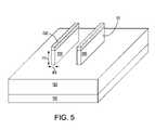
- FIG. 5is a perspective view depicting a fin structure having a width of less than 20 nm, wherein a dielectric fin cap is present on an upper surface of the fin structure and sidewalls of the fin structure are exposed, as used in one embodiment of a method for forming a finFETs device, in accordance with the present invention.
- FIG. 6is a perspective view depicting forming a gate structure atop a portion of the fin structure, wherein a remaining portion of the sidewalls of the fin structure are exposed, in accordance with one embodiment of the present invention.
- FIG. 7is a perspective view depicting forming a dielectric spacer in direct contact with the gate structure, in accordance with one embodiment of the present invention.
- FIG. 8is a perspective view depicting forming in-situ doped semiconductor material on the exposed sidewalls of the fin structure, in accordance with one embodiment of the present invention.
- FIG. 9Ais a perspective view depicting one embodiment of diffusing dopant from the in-situ doped semiconductor material into the fin structure to form extension regions, in accordance with the present invention.
- FIG. 9Bis a side-cross sectional view along section line Y-Y of FIG. 9A .
- the present inventionrelates to a method for forming a planar semiconductor device on a semiconductor on insulator (SOI) substrate having an extremely thin semiconductor on insulator (ETSOI) layer.
- An extremely thin semiconductor on insulator (ETSOI) layeris the semiconductor layer that is present atop the buried insulating layer of an SOI substrate, wherein the ETSOI layer has a thickness of 10 nm or less.
- source and drain extension regionsare formed in the ETSOI layer using an in situ doped epitaxial growth process followed by an annealing process to drive the dopant from the in-situ doped epitaxial semiconductor material into the ETSOI layer to provide extension regions without utilizing ion implantation.
- a methodis provided for forming a finFET structure without using ion implantation.
- semiconductor devicerefers to an intrinsic semiconductor material that has been doped, that is, into which a doping agent has been introduced, giving it different electrical properties than the intrinsic semiconductor.
- Dopinginvolves adding dopant atoms to an intrinsic semiconductor, which changes the electron and hole carrier concentrations of the intrinsic semiconductor at thermal equilibrium. Dominant carrier concentration in an extrinsic semiconductor determines the conductivity type of the semiconductor.
- a field effect transistoris a transistor in which output current, i.e., source-drain current, is controlled by the voltage applied to the gate.
- a field effect transistorhas three terminals, i.e., gate, source and drain.
- conductivity typedenotes a dopant region being p-type or n-type.
- p-typerefers to the addition of impurities to an intrinsic semiconductor that creates deficiencies of valence electrons.
- examples of n-type dopants, i.e., impuritiesinclude but are not limited to: boron, aluminum, gallium and indium.
- n-typerefers to the addition of impurities that contributes free electrons to an intrinsic semiconductor
- impuritiesinclude but are not limited to antimony, arsenic and phosphorous.
- a “gate structure”means a structure used to control output current (i.e., flow of carriers in the channel) of a semiconducting device through electrical or magnetic fields.
- a “gate dielectric”is a layer of an insulator between the semiconductor device substrate of a planar device, or fin structure, and the gate conductor.
- a “gate conductor”means a conductive structure of the gate structure on the gate dielectric.
- channelis the region underlying the gate structure and between the source and drain of a semiconductor device that becomes conductive when the semiconductor device is turned on.
- drainmeans a doped region in semiconductor device located at the end of the channel, in which carriers are flowing out of the transistor through the drain.
- the term “source”is a doped region in the semiconductor device, in which majority carriers are flowing into the channel.
- the term “raised” in combination with source and/or draindenotes that the source and/or drain region is formed on a semiconductor material layer that is present on an upper surface of the substrate on which the gate dielectric is present.
- a “fin structure”refers to a semiconductor material, which is employed as the body of a semiconductor device, in which the gate structure is positioned around the fin structure such that charge flows down the channel on the two sidewalls of the fin structure and optionally along the top surface of the fin structure.
- an “anisotropic etch process”denotes a material removal process in which the etch rate in the direction normal to the surface to be etched is greater than in the direction parallel to the surface to be etched.
- the term “selective” in reference to a material removal processdenotes that the rate of material removal for a first material is greater than the rate of removal for at least another material of the structure to which the material removal process is being applied.
- Epitaxy growth and/or depositionmeans the growth of a semiconductor material on a deposition surface of a semiconductor material, in which the semiconductor material being grown has the same crystalline characteristics as the semiconductor material of the deposition surface.
- Si:Cor “carbon-doped silicon” as used herein refers to silicon having substitutional carbon atoms located therein.
- the substitutional carbon atoms and the silicon atomsform a silicon-carbon alloy, which is a semiconductor material.
- insulating and dielectricdenote a material having a room temperature conductivity of less than about 10 ⁇ 10 ( ⁇ -m) ⁇ 1 .
- first elementsuch as a first structure
- second elementsuch as a second structure
- first elementsuch as a first structure
- second elementsuch as a second structure
- intervening elementssuch as an interface structure
- FIGS. 1-4depict one embodiment of a method of forming a semiconductor device on semiconductor layer, i.e., first semiconductor layer 20 , having a thickness of less than 10 nm, in which the method does not use ion implantation to provide the source and drain regions and the extensions regions 45 of the semiconductor device. It has been determined that when implanting dopants into semiconductor layers that have a thickness of 10 nm or less that the ion implantation amorphizes the semiconductor layer. Recrystallizing the amorphous semiconductor layer is difficult, because of the limited amount of crystal seed layer that is available in semiconductor layers having a thickness of less than 10 nm that have been ion implanted into an amorphous crystal structure.
- the presence of an amorphous semiconductor material in a semiconductor deviceresults in the semiconductor device having a high external resistance. Further, the resistance of the semiconductor device is increased by defects in the semiconductor layer that are produced by ion implantation. The ion implantation may also damage the gate dielectric.
- the method disclosed hereinovercomes the disadvantages that result from ion implantation, by forming the source and drain regions in an ETSOI layer, i.e., first semiconductor layer 20 , using an in-situ doped epitaxial semiconductor growth process followed by an annealing process.
- the annealing processdrives the dopant from the in-situ doped epitaxial semiconductor material 21 , i.e., in-situ doped epitaxial semiconductor raised source and drain regions, into the first semiconductor layer 20 to provide extension regions 45 .
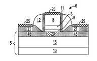
- FIG. 1illustrates the results of the initial processing steps that produce a substrate 5 , i.e., semiconductor on insulator (SOI) substrate, in which a substrate 5 comprises at least a first semiconductor layer 20 (hereafter referred to as an ETSOI layer 20 ) overlying a dielectric layer 15 , wherein the ETSOI layer 20 has a thickness of less than 10 nm.
- a second semiconductor layer 10may be present underlying the dielectric layer 15 .
- the ETSOI layer 20may comprise any semiconducting material including, but not limited to Si, strained Si, SiC, SiGe, SiGeC, Si alloys, Ge, Ge alloys, GaAs, InAs, and InP, or any combination thereof.
- the ETSOI layer 20may be thinned to a desired thickness by planarization, grinding, wet etch, dry etch, oxidation followed by oxide etch, or any combination thereof.
- One method of thinning the ETSOI layer 20is to oxidize the Si by a thermal dry or wet oxidation process, and then wet etch the oxide layer using a hydrofluoric acid mixture. This process can be repeated to achieve the desired thickness.
- the ETSOI layer 20has a thickness ranging from 1.0 nm to 10.0 nm. In another embodiment, the ETSOI layer 20 has a thickness ranging from 1.0 nm to 5.0 nm. In a further embodiment, the ETSOI layer 20 has a thickness ranging from 3.0 nm to 8.0 nm.
- the second semiconductor layer 10may be a semiconducting material including, but not limited to Si, strained Si, SiC, SiGe, SiGeC, Si alloys, Ge, Ge alloys, GaAs, InAs, InP as well as other III/V and II/VI compound semiconductors.
- the dielectric layer 15 that may be present underlying the ETSOI layer 20 and atop the second semiconductor layer 10may be formed by implanting a high-energy dopant into the substrate 5 and then annealing the structure to form a buried insulating layer, i.e., dielectric layer 15 .
- the dielectric layer 15may be deposited or grown prior to the formation of the ETSOI layer 20 .
- the substrate 5may be formed using wafer-bonding techniques, where a bonded wafer pair is formed utilizing glue, adhesive polymer, or direct bonding.
- FIG. 2depicts forming a gate structure 6 directly on the first semiconductor layer, in accordance with one embodiment of the present invention.
- the gate structure 6can be formed using deposition, photolithography and a selective etching process. Specifically, a pattern is produced by applying a photoresist to the surface to be etched; exposing the photoresist to a pattern of radiation; and then developing the pattern into the photoresist utilizing a resist developer. Once the patterning of the photoresist is completed, the sections covered by the photoresist are protected while the exposed regions are removed using a selective etching process that removes the unprotected regions.
- a hard maskhereafter referred to as a dielectric cap 4
- the dielectric cap 4may be formed by first depositing a dielectric hard mask material, like SiN or SiO 2 , atop a layer of gate electrode material and then applying a photoresist pattern to the hard mask material using a lithography process steps. The photoresist pattern is then transferred into the hard mask material using a dry etch process forming the dielectric cap 4 . Next the photoresist pattern is removed and the dielectric cap 4 pattern is then transferred into the gate electrode material during a selective etching process. The dielectric cap 4 may be removed by a wet or dry etch prior to the silicidation process. Alternatively, the first and second gate structure 6 can be formed by other patterning techniques such as spacer image transfer.
- the gate structure 6may include at least a gate conductor atop a gate dielectric 9 .
- Gate conductormay be a metal gate electrode 3 .
- the metal gate electrode 3may be any conductive metal including, but not limited to W, Ni, Ti, Mo, Ta, Cu, Pt, Ag, Au, Ru, Ir, Rh, and Re, and alloys that include at least one of the aforementioned conductive elemental metals.
- the gate structuremay further include a second conductive material 8 atop the metal gate electrode 3 .
- the second conductive material 8may be a doped semiconductor material, such as a doped silicon containing material, e.g., doped polysilicon.
- the gate conductor of the gate structureis typically present on a gate dielectric 9 .
- the gate dielectric 9may be a dielectric material, such as SiO 2 , or alternatively high-k dielectrics, such as oxides of Ta, Zr, Al or combinations thereof
- the gate dielectric 9is comprised of an oxide, such as SiO 2 , ZrO 2 , Ta 2 O 5 or Al 2 O 3 .
- the gate dielectric 9has a thickness ranging from 1 nm to 10 nm. In another embodiment, the gate dielectric 9 has a thickness ranging from 1.5 nm to 2.5 nm.
- a set of first spacers 11can be formed in direct contact with the sidewalls of the gate structure 6 .
- the first spacers 11are typically narrow having a width ranging from 2.0 nm to 15.0 nm.
- the first spacer 11can be formed using deposition and etch processing steps.
- the first spacer 11may be composed of a dielectric, such as nitride, oxide, oxynitride, or a combination thereof.
- the thickness of the first spacer 11determines the proximity of the subsequently formed raised source/drain (RSD) regions to the channel of the device.
- RSDraised source/drain
- FIG. 3depicts one embodiment of forming an in-situ doped semiconductor material 21 on exposed surfaces of the ETSOI layer 20 that are adjacent to the gate structure 6 .
- the in-situ doped semiconductor material 21is formed using an epitaxial growth process.
- the depositing atomsarrive at the surface of the ETSOI layer 20 with sufficient energy to move around on the surface and orient themselves to the crystal arrangement of the atoms of the deposition surface.
- an epitaxial film deposited on a ⁇ 100 ⁇ crystal surfacewill take on a ⁇ 100 ⁇ orientation.
- the wafer surfacehas an amorphous surface layer, possibly the result of implanting, the depositing atoms have no surface to align to, resulting in the formation of polysilicon instead of single crystal silicon.
- a number of different sourcesmay be used for the deposition of epitaxial silicon. Silicon sources for epitaxial growth include silicon tetrachloride, dichlorosilane (SiH 2 Cl 2 ), and silane (SiH 4 ).
- the temperature for epitaxial silicon depositiontypically ranges from 550° C. to 900° C. Although higher temperature typically results in faster deposition, the faster deposition may result in crystal defects and film cracking.
- the in-situ doped semiconductor material 21may be provided by selective-epitaxial growth of SiGe atop the ETSOI layer 20 .
- the Ge content of the epitaxial grown SiGemay range from 5% to 60%, by atomic weight %. In another embodiment, the Ge content of the epitaxial grown SiGe may range from 10% to 40%.
- the epitaxial grown SiGemay be under an intrinsic compressive strain, in which the compressive strain is produced by a lattice mismatch between the larger lattice dimension of the SiGe and the smaller lattice dimension of the layer on which the SiGe is epitaxially grown. In one embodiment, the epitaxial grown SiGe produces a compressive strain in the portion of the ETSOI layer 20 , in which the channel of a semiconductor device, such as a pFET device, is subsequently formed.
- the in-situ doped semiconductor material 21is doped with a first conductivity type dopant during the epitaxial growth process.
- the in-situ doped semiconductor material 21provides the raised source and drain regions of a semiconductor device, P-type MOSFET devices are produced by doping the in-situ doped semiconductor material 21 with elements from group III of the Periodic Table of Elements.
- the group III elementis boron, aluminum, gallium or indium.
- the dopantmay be boron present in a concentration ranging from 1 ⁇ 10 18 atoms/cm 3 to 2 ⁇ 10 21 atoms/cm 3 .
- the in-situ doped semiconductor material 21is composed of SiGe and is doped with boron to provide the raised source and drain regions of a p-type conductivity field effect transistor.
- the in-situ doped semiconductor material 21is composed of epitaxially grown Si:C or carbon doped silicon.
- the carbon (C) content of the epitaxial grown Si:Cranges from 0.3% to 10%, by atomic weight %. In another embodiment, the carbon (C) content of the epitaxial grown Si:C may range from 1% to 2%.
- the epitaxial grown Si:Cmay be under an intrinsic tensile strain, in which the tensile strain is produced by a lattice mismatch between the smaller lattice dimension of the Si:C and the larger lattice dimension of the layer on which the Si:C is epitaxially grown. In one embodiment, the epitaxial grown Si:C produces a tensile strain in the ETSOI layer 20 , in which the channel of a semiconductor device, such as a nFET device, is subsequently formed.
- the in-situ doped semiconductor material 21is doped with a second conductivity type dopant during the epitaxial growth process.
- the in-situ semiconductor material 21provides the raised source and drain regions of a semiconductor device, in which n-type MOSFET devices are produced by doping the in-situ doped semiconductor material 21 with elements from group V of the Periodic Table of Elements.
- the group V elementis phosphorus, antimony or arsenic.
- FIG. 4depicts one embodiment of diffusing dopant from the in-situ doped semiconductor material 21 into the ETSOI layer 20 to form extension regions 45 .
- the dopant from the in-situ doped semiconductor material 21is diffused into the ETSOI layer 20 by an annealing processes including, but not limited to: rapid thermal annealing, furnace annealing, flash lamp annealing, laser annealing, or any suitable combination of thereof.
- thermal annealing to diffuse the dopant from the in-situ doped semiconductor material 21 into the ETSOI layer 20is conducted at a temperature ranging from about 850° C. to about 1350° C.
- the extension regions 45 that are formed in the ETSOI layer 20have a p-type conductivity.
- the dopant concentration of the extension regions 45 having the p-type conductivityranges from 1 ⁇ 10 19 atoms/cm 3 to 2 ⁇ 10 21 atoms/cm 3 .
- the extension regions 45have the p-type conductivity ranging from 2 ⁇ 10 19 atoms/cm 3 to 5 ⁇ 10 20 atoms/cm 3 .
- the extension regions 45 that are formed in the ETSOI layer 45have an n-type conductivity.
- the dopant concentration of the extension regions 45 having the n-type conductivityranges from 1 ⁇ 10 19 atoms/cm 3 to 2'10 21 atoms/cm 3 .
- the extension regions 45have the p-type conductivity ranging from 2 ⁇ 10 19 atoms/m 3 to 5 ⁇ 10 20 atoms/cm 3 .
- the extension regions 45have a depth that extends the entire depth of the ETSOI layer 20 . Therefore, the extension regions 45 have a depth of less than 10 nm, typically being 3 nm to 8 nm in depth, as measured from the upper surface of the ETSOI layer 20 .
- FIG. 4depicts removing the dielectric cap 4 from the gate structure 6 and forming a second spacer 12 in direct contact with the first spacer 11 .
- the dielectric cap 4may be removed using a selective etch process.
- the width of the second spacers 12is selected to ensure that subsequent silicidation processes do not result in a silicide bridge from the contacts to the raised source and drain regions provided by the in-situ doped semiconductor material 21 to the conductive features of the gate structure 6 .
- the second spacers 12may be formed by depositing a conformal dielectric film and using a highly directional dry etch process.
- the second spacers 12may be composed of a dielectric such as a nitride, oxide, oxynitride, high-k dielectric, or a combination thereof.
- Silicides 25are then formed on the raised source and drain regions of the device, i.e., the in-situ doped semiconductor material 21 .
- Silicide formationtypically requires depositing a refractory metal such as cobalt, nickel, or titanium onto the surface of a Si-containing material.
- a refractory metalsuch as cobalt, nickel, or titanium onto the surface of a Si-containing material.
- the structureis subjected to an annealing step using conventional processes such as, but not limited to, rapid thermal annealing.
- the deposited metalreacts with Si forming a metal silicide.
- the remaining unreacted metalis removed by an etch process selective to silicides 25 and spacers 12 .
- a gate silicidemay also be formed on the gate conductor.
- a layer of dielectric materialcan be blanket deposited atop the entire substrate and planarized.
- the blanket dielectricmay be selected from the group consisting of silicon-containing materials such as SiO 2 , Si 3 N 4 , SiO x N y , SiC, SiCO, SiCOH, and SiCH compounds; the above-mentioned silicon-containing materials with some or all of the Si replaced by Ge; carbon-doped oxides; inorganic oxides; inorganic polymers; hybrid polymers; organic polymers such as polyamides or SiLKTM; other carbon-containing materials; organo-inorganic materials such as spin-on glasses and silsesquioxane-based materials; and diamond-like carbon (DLC, also known as amorphous hydrogenated carbon, ⁇ -C:H).
- silicon-containing materialssuch as SiO 2 , Si 3 N 4 , SiO x N y , SiC, SiCO, SiCOH, and SiCH compounds
- blanket dielectricexamples include: any of the aforementioned materials in porous form, or in a form that changes during processing to or from being porous and/or permeable to being non-porous and/or non-permeable.
- the deposited dielectricis then patterned and etched to form via holes to the various source/drain and gate conductor regions of the device.
- interconnectsare formed by depositing a conductive metal into the via holes using deposition methods, such as CVD or plating.
- the conductive metalmay include, but is not limited to: tungsten, copper, aluminum, silver, gold and alloys thereof.
- the above processmay provide a planar semiconductor device that includes a substrate 5 having a layer of semiconductor material (ETSOI layer 20 ) atop an insulating layer 15 , wherein the layer of semiconductor material has at thickness of less than 10.0 nm.
- a gate structure 6is present on the semiconductor material.
- the planar semiconductor deviceincludes doped epitaxial raised source and drain regions (in-situ doped semiconductor material 21 ) that are present atop the semiconductor material, and extension diffusions (extension regions 45 ) extending from the doped epitaxial raised source and drain regions into the semiconductor material.
- FIGS. 5-9Bdepict one embodiment of a method of fabricating a finFET semiconductor device having a fin structure 200 with a width W 1 of less than 20 nm, in which the method does not use ion implantation to provide the source and drain regions (in-situ doped epitaxial semiconductor material 210 ) and the extensions regions 45 of the device.
- FinFET formationtypically requires ion implantation to form source and drain extension regions. Ion implantation typically tends to amorphize the entire fin structure and generates implant-related defects. It is difficult to recrystallize the amorphous semiconductor and to eliminate implant defects during the subsequent low thermal budget anneal process that are typically utilized in finFET manufacturing.
- the method disclosed hereinovercomes the disadvantages that result from ion implantation by forming the source and drain extensions in the fin structure using an in-situ doped epitaxial growth process followed by an annealing process, wherein the annealing process drives the dopant into the fin structure to form extension regions.
- FIG. 5depicts an initial structure used in one embodiment of a method for forming a finFET device.
- the initial structuremay include a fin structure 200 present atop a dielectric layer 150 .
- a dielectric fin cap 230may be optionally present on the fin structure 200 .
- the fin structure 200 and the dielectric layer 150may be provided from an SOI substrate, in which the top semiconductor layer of the SOI substrate provides the fin structure 200 .
- the SOI substratetypically includes a bottom semiconductor layer 100 and a top semiconductor layer 200 (hereafter referred to as an SOI layer 200 ) that are electrically isolated from each other by a buried insulating layer (hereafter referred to as a dielectric layer 150 ).
- the SOI layer 200 and the bottom semiconductor layer 100may comprise at least one of Si, Ge alloys, SiGe, GaAs, InAs, InP, SiCGe, SiC as well as other III/V or II/VI compound semiconductors.
- the SOI layer 200 and bottom semiconductor layer 100may comprise the same or different materials.
- the dielectric layer 150 separating the SOI layer 200 and the bottom semiconductor layer 100may be a crystalline or non-crystalline oxide, nitride, oxynitride, or any other insulating material.
- the SOI substrate employed in the present inventionmay be formed utilizing a layer transfer process including a bonding step.
- an implantation processsuch as SIMOX (Separation by IMplantation of OXygen) can be used in forming the SOI substrate.
- the thickness of the various layers of the SOI substratemay vary depending on the technique used in forming the same.
- the SOI layer 200has a thickness ranging from 3 nm to 100 nm
- the dielectric layer 200also referred to as buried dielectric layer
- the thickness of the bottom semiconductor layer 100 of the SOI substratemay range from 10 nm to 500 nm.
- the bulk semiconductor substratecomprises at least one of Si, Ge alloys, SiGe, GaAs, InAs, InP, SiCGe, SiC as well as other III/V or II/VI compound semiconductors.
- a layer of the dielectric material that provides the dielectric fin cap 230is deposited atop the SOI substrate.
- the dielectric fin cap 230may be composed of a nitride, oxide, oxynitride material, and/or any other suitable dielectric layer.
- the dielectric fin cap 230may comprise a single layer of dielectric material or multiple layers of dielectric materials.
- the dielectric fin cap 230can be formed by a deposition process, such as chemical vapor deposition (CVD) and/or atomic layer deposition (ALD).
- Chemical vapor depositionis a deposition process in which a deposited species is formed as a result of chemical reaction between gaseous reactants at greater than room temperature (25° C. to 900° C.); wherein solid product of the reaction is deposited on the surface on which a film, coating, or layer of the solid product is to be formed.
- Variations of CVD processesinclude, but not limited to, Atmospheric Pressure CVD (APCVD), Low Pressure CVD (LPCVD) and Plasma Enhanced CVD (EPCVD), Metal-Organic CVD (MOCVD) and combinations thereof may also be employed.
- APCVDAtmospheric Pressure CVD
- LPCVDLow Pressure CVD
- EPCVDPlasma Enhanced CVD
- MOCVDMetal-Organic CVD
- the dielectric fin cap 230may be formed using a growth process, such as thermal oxidation or thermal nitridation.
- the dielectric fin cap 230may have a thickness ranging from 1 nm to 100 nm.
- the dielectric fin cap 230is composed of an oxide, such as SiO 2 , that is formed by chemical vapor deposition to a thickness on the order of 25 nm to 50 nm. In yet another embodiment, no dielectric fin cap 230 is present.
- a photolithography and etch process sequence applied to the dielectric fin cap 230 and the SOI substratemay provide the initial structure that is depicted in FIG. 5 .
- a photoresist maskis formed overlying the layer of the dielectric material that provides dielectric fin cap 230 and is present overlying the SOI layer 200 of the substrate, in which the portion of the dielectric material that is underlying the photoresist mask provides the dielectric fin cap 230 , and the portion of the SOI layer 200 that is underlying the photoresist mask provides the fin structure 200 .
- a photoresist layeris first positioned on the layer of the dielectric material that provides dielectric fin cap 230 .
- the photoresist layermay be provided by a blanket layer of photoresist material that is formed utilizing a deposition process such as, for example, CVD, PECVD, evaporation or spin-on coating.
- the blanket layer of photoresist materialis then patterned to provide the photoresist mask utilizing a lithographic process that may include exposing the photoresist material to a pattern of radiation and developing the exposed photoresist material utilizing a resist developer.
- an etching processmay remove the unprotected portions of the dielectric material that provides the dielectric fin cap 230 followed by removing the unprotected portion of the SOI layer 200 selective to the underlying buried insulating layer, i.e., dielectric layer 150 .
- the transferring of the pattern provided by the photoresist into the underlying structuresmay include an anisotropic etch.
- the anisotropic etchmay include reactive-ion etching (RIE).
- RIEReactive Ion Etching
- RIEis a form of plasma etching in which during etching the surface to be etched is placed on the RF powered electrode.
- the surface to be etchedtakes on a potential that accelerates the etching species extracted from plasma toward the surface, in which the chemical etching reaction is taking place in the direction normal to the surface.
- anisotropic etchingthat can be used at this point of the present invention include ion beam etching, plasma etching or laser ablation.
- the fin structure 200can be formed by spacer imaging transfer technique well-known in the art.
- the fin structure 200may have a height H 1 ranging from 5 nm to 200 nm. In one embodiment, the fin structure 200 has a height H 1 ranging from 10 nm to 100 nm. In another embodiment, the fin structure 200 has a height H 1 ranging from 20 nm to 50 nm. In one embodiment, the fin structure 200 has a width W 1 of less than 20 nm. In another embodiment, the fin structure 200 has a width W 1 ranging from 3 nm to 8 nm.
- FIG. 6depicts forming a gate structure 60 on the fin structure 200 and the dielectric fin cap 230 .
- the gate structure 60includes a gate dielectric 90 in contact with at least the fin structure 200 , a gate conductor 80 on the gate dielectric 90 , and a gate dielectric cap 40 on the gate conductor 80 .
- the gate structure 60may be formed by forming blanket material layers for the gate dielectric 90 , gate conductor 80 , and gate dielectric cap 40 to provide a gate stack, and patterning and etching the gate stack to provide the gate structure 60 .
- the gate structure 60can be formed utilizing photolithography and etch process steps.
- a patternis produced by applying a photoresist to the surface to be etched; exposing the photoresist to a pattern of radiation; and then developing the pattern into the photoresist utilizing conventional resist developer.
- the sections covered by the photoresistare protected while the exposed regions are removed using a selective etching process that removes the unprotected regions.
- the portion of the gate stack that is removed to provide the gate structure 60exposes the sidewalls S 1 of the fin structure 220 .
- the gate dielectric 90is typically positioned on at least a portion of the sidewalls S 1 of the fin structure 200 .
- the gate dielectric 90may be formed by a thermal growth process such as, for example, oxidation, nitridation or oxynitridation.
- the gate dielectric 90may also be formed by a deposition process such as, for example, chemical vapor deposition (CVD), plasma-assisted CVD, metal organic chemical vapor deposition (MOCVD), atomic layer deposition (ALD), evaporation, reactive sputtering, chemical solution deposition and other like deposition processes.
- the gate dielectric 90is deposited using a conformal deposition process.
- conformaldenotes a layer having a thickness that does not deviate from greater than or less than 20% of an average value for the thickness of the layer.
- the gate dielectric 90may also be formed utilizing any combination of the above processes.
- the gate dielectric 90may be comprised of an insulating material having a dielectric constant of 4.0 or greater. In another embodiment, the gate dielectric 90 is comprised of an insulating material having a dielectric constant greater than 7.0.
- the dielectric constants mentioned hereinare relative to a vacuum at room temperature.
- the gate dielectric 90 employed in the present inventionincludes, but is not limited to: an oxide, nitride, oxynitride and/or silicates including metal silicates, aluminates, titanates and nitrides.
- the oxidewhen the gate dielectric 90 is comprised of an oxide, the oxide may be selected from the group including, but not limited to SiO 2 , HfO 2 , ZrO 2 , Al 2 O 3 , TiO 2 , La 2 O 3 , SrTiO 3 , LaAlO 3 , Y 2 O 3 and mixture thereof.
- the physical thickness of the gate dielectric 90may vary, but typically, the gate dielectric 90 has a thickness ranging from 1 nm to 10 nm. In another embodiment, the gate dielectric 90 has a thickness ranging from 1 nm to 3 nm.
- the gate conductor 80 of the gate structure 60is formed on the gate dielectric 90 utilizing a deposition process, such as physical vapor deposition (PVD), CVD or evaporation.
- the gate conductor 80may be composed of polysilicon, SiGe, a silicide, a metal or a metal-silicon-nitride, such as Ta—Si—N. Examples of metals that can be used as the gate conductor 80 include, but are not limited to Al, W, Cu, Ti or other like conductive metals.
- the gate conductor 80comprises Ti, Zr, Hf, V, Nb, Ta, TiN, TaN or a combination thereof.
- the gate conductor 80may be doped or undoped.
- the physical thickness of the gate conductor 80may range from 1 nm to 10 nm. In another embodiment, the gate conductor 80 has a thickness ranging from 1 nm to 3 nm.
- the gate dielectric cap 40may be composed of a nitride, oxide, oxynitride material, and/or any other suitable dielectric layer. Gate dielectric cap 40 may comprise a single layer of dielectric material or multiple layers of dielectric materials. The dielectric layer can be formed by a deposition process, such as chemical vapor deposition (CVD) and/or atomic layer deposition (ALD). Alternatively, the gate dielectric cap 40 may be formed using a growth process, such as thermal oxidation or thermal nitridation. The gate dielectric cap 40 may have a thickness ranging from 1 nm to 100 nm. In one embodiment, the gate dielectric cap 40 is composed of a nitride, such as SiN, that is formed by chemical vapor deposition to a thickness on the order of 25 nm to 50 nm.
- a nitridesuch as SiN
- FIG. 7depicts forming a first spacer 110 in direct contact with the gate structure 60 .
- the first spacer 110may be formed by depositing a conformal layer of dielectric material, such as oxides, nitrides or oxynitrides.
- the etching processis an anisotropic etching process, such as reactive ion etch.
- the first spacer 110may have a width ranging from 1 nm to 10 nm, typically ranging from 1 nm to 5 nm.
- FIG. 8depicts forming in-situ doped semiconductor material 210 on the sidewalls S 1 of the fin structure 200 that are exposed.
- in-situ doped semiconductor material 210is formed using an epitaxial growth process.
- a number of different sourcesmay be used for the deposition of epitaxial silicon. Silicon sources for epitaxial growth include silicon tetrachloride, dichlorosilane (SiH 2 Cl 2 ), and silane (SiH 4 ).
- the in-situ doped semiconductor material 210may be provided by selective-epitaxial growth of SiGe on the exposed sidewalls S 1 of the fin structure 200 .
- the Ge content of the epitaxial grown SiGemay range from 5% to 70%, by atomic weight %. In another embodiment, the Ge content of the epitaxial grown SiGe may range from 10% to 45%. In one embodiment, the epitaxial grown SiGe produces a compressive strain in the portion of the fin structure 200 , in which the channel of a semiconductor device, such as a p-type conductivity finFET, is subsequently formed.
- in-situ doped semiconductor material 210is doped with a first conductivity type dopant during the epitaxial growth process.
- the in-situ doped semiconductor material 210provides the source and drain regions of a finFET device.
- P-type finFET devicesare produced by doping the in-situ doped semiconductor material 210 with elements from group III of the Periodic Table of Elements.
- the group III elementis boron, aluminum, gallium or indium.
- the dopantmay be boron present in a concentration ranging from 1 ⁇ 10 19 atoms/cm 3 to 2 ⁇ 10 21 atoms/cm 3 .
- the in-situ doped semiconductor material 210is composed of SiGe and is doped with boron to provide the raised source and drain regions of a p-type conductivity finFET.
- the in-situ doped semiconductor material 210is composed of epitaxially grown Si:C or carbon doped silicon.
- the carbon (C) content of the epitaxial grown Si:Cranges from 0.5% to 10%, by atomic weight %. In another embodiment, the carbon (C) content of the epitaxial grown Si:C may range from 1% to 2%.
- the epitaxial grown Si:Cproduces a tensile strain in the portion of the fin structure 200 , in which the channel of a semiconductor device, such as an n-type conductivity finFET, is subsequently formed.
- the in-situ doped semiconductor material 21is doped with a second conductivity type dopant during the epitaxial growth process.
- the in-situ semiconductor material 21provides the source and drain regions of a finFET device.
- N-type finFET devicesare produced by doping the in-situ doped semiconductor material 21 with elements from group V of the Periodic Table of Elements.
- the group V elementis phosphorus, antimony or arsenic.
- FIGS. 9A and 9 bdepict one embodiment of diffusing dopant from the in-situ doped semiconductor material 210 into the fin structure 200 to form extension regions 450 .
- the dopant from the in-situ doped semiconductor material 210is diffused into the fin structure 200 by an annealing processes including, but not limited to rapid thermal annealing, furnace annealing, flash lamp annealing or laser annealing.
- thermal annealing to diffuse the dopant from the in-situ doped semiconductor material 210 into the fin structure 200is conducted at a temperature ranging from about 850° C. to about 1350° C.
- the extension regions 450 that are formed in the fin structure 200have a p-type conductivity. In another embodiment, in which the in-situ doped semiconductor material 210 is doped to an n-type conductivity, the extension regions 450 that are formed in the fin structure 200 have an n-type conductivity.
- the dopant concentration of the extension regions 450ranges from 1 ⁇ 10 19 atoms/cm 3 to 5 ⁇ 10 21 atoms/cm 3 . In another embodiment, the extension regions 450 have a dopant concentration ranging from 2 ⁇ 10 19 atoms/cm 3 to 2 ⁇ 10 20 atoms/cm 3 .
- the above processmay provide a finFET semiconductor device that includes a fin structure 200 having a width W 2 of less than 10.0 nm.
- a gate structure 60is present overlying a portion of the fin structure 200 , in which a dielectric spacer 110 is present in direct contact with the gate structure 60 .
- Doped epitaxial source and drain regionsare present in direct contact with the sidewalls S 1 of the fin structure 200 and in direct contact with the dielectric spacer 11 .
- Extension diffusions 450are present extending from the doped epitaxial source and drain regions 210 into the fin structure 200 .
Landscapes
- Thin Film Transistor (AREA)
- Insulated Gate Type Field-Effect Transistor (AREA)
Abstract
Description
- The present disclosure relates generally to semiconductor devices. More particularly, the present disclosure relates to scaling of semiconductor devices.
- In order to be able to make integrated circuits (ICs), such as memory, logic, and other devices, of higher integration density than currently feasible, one has to find ways to further downscale the dimensions of field effect transistors (FETs), such as metal-oxide-semiconductor field effect transistors (MOSFETs) and complementary metal oxide semiconductors (CMOS). Scaling achieves compactness and improves operating performance in devices by shrinking the overall dimensions and operating voltages of the device while maintaining the device's electrical properties. Additionally, all dimensions of the device must be scaled simultaneously in order to optimize the electrical performance of the device. With conventional planar FET scaling reaching fundamental limits, the semiconductor industry is looking at more unconventional geometries that will facilitate continued device performance improvements.
- A method of fabricating a semiconductor device is provided in which the channel of the device is present in an extremely thin semiconductor on insulator (ETSOI) layer, i.e., a semiconductor containing layer having a thickness of less than 10.0 nm. In one embodiment, the method may begin with providing a substrate comprising at least a first semiconductor layer overlying a dielectric layer, wherein the first semiconductor layer has a thickness of less than 10.0 nm. A gate structure is formed directly on the first semiconductor layer. An in-situ doped semiconductor material is formed on the first semiconductor layer adjacent to the gate structure. The dopant from the in-situ doped semiconductor material is diffused into the first semiconductor layer to form extension regions.
- In another aspect, a planar semiconductor device is provided that includes a substrate having a layer of semiconductor material atop an insulating layer, wherein the layer of semiconductor material has at thickness of less than 10.0 nm. A gate structure is present on the layer of semiconductor material. The planar semiconductor device includes doped epitaxial raised source and drain regions that are present atop the layer of semiconductor material and on opposing sides of the gate structure. Extension diffusions are present extending from the doped epitaxial raised source and drain regions into the layer of semiconductor material.
- In another embodiment, a method of fabricating a semiconductor device is provided that includes providing a fin structure having a width of less than 20 nm, wherein a dielectric fin cap is present on an upper surface of the fin structure and sidewalls of the fin structure are exposed. A gate structure is formed atop a portion of the fin structure, where a remaining portion of the sidewalls of the fin structure is exposed.
- In-situ doped semiconductor material is formed on the exposed sidewalls of the fin structure. The dopants from the in-situ doped semiconductor material diffuse into the fin structure to form extension regions.
- In another aspect, a finFET semiconductor device is provided that includes a fin structure having a width of less than 20 nm. A gate structure is present atop a portion of the fin structure. A dielectric spacer is present in direct contact with the gate structure. The finFET semiconductor device further includes doped epitaxial source and drain regions that are present in direct contact with the sidewalls of the fin structure and in direct contact with the dielectric spacer. Extension diffusions extend from the doped epitaxial source and drain regions into the fin structure.
- The following detailed description, given by way of example and not intended to limit the invention solely thereto, will best be appreciated in conjunction with the accompanying drawings, wherein like reference numerals denote like elements and parts, in which:
FIG. 1 is a side cross-sectional view depicting providing a substrate comprising at least a first semiconductor layer atop a dielectric layer, wherein the first semiconductor layer has a thickness of less than 10 nm, as used in one embodiment of a method for forming a planar semiconductor device, in accordance with the present invention.FIG. 2 is a side cross-sectional view depicting forming a gate structure directly on the first semiconductor layer, in accordance with one embodiment of the present invention.FIG. 3 is a side cross-sectional view depicting forming an in-situ doped semiconductor material on the first semiconductor layer adjacent to the gate structure, in accordance with one embodiment of the present invention.FIG. 4 is a side cross-sectional view depicting diffusing dopant from the in-situ doped semiconductor material into the first semiconductor layer to form extension regions, in accordance with one embodiment of the present invention.FIG. 5 is a perspective view depicting a fin structure having a width of less than 20 nm, wherein a dielectric fin cap is present on an upper surface of the fin structure and sidewalls of the fin structure are exposed, as used in one embodiment of a method for forming a finFETs device, in accordance with the present invention.FIG. 6 is a perspective view depicting forming a gate structure atop a portion of the fin structure, wherein a remaining portion of the sidewalls of the fin structure are exposed, in accordance with one embodiment of the present invention.FIG. 7 is a perspective view depicting forming a dielectric spacer in direct contact with the gate structure, in accordance with one embodiment of the present invention.FIG. 8 is a perspective view depicting forming in-situ doped semiconductor material on the exposed sidewalls of the fin structure, in accordance with one embodiment of the present invention.FIG. 9A is a perspective view depicting one embodiment of diffusing dopant from the in-situ doped semiconductor material into the fin structure to form extension regions, in accordance with the present invention.FIG. 9B is a side-cross sectional view along section line Y-Y ofFIG. 9A .- Detailed embodiments of the present invention are disclosed herein; however, it is to be understood that the disclosed embodiments are merely illustrative of the invention that may be embodied in various forms. In addition, each of the examples given in connection with the various embodiments of the invention is intended to be illustrative, and not restrictive. Further, the figures are not necessarily to scale, some features may be exaggerated to show details of particular components. Therefore, specific structural and functional details disclosed herein are not to be interpreted as limiting, but merely as a representative basis for teaching one skilled in the art to variously employ the present invention.
- In one embodiment, the present invention relates to a method for forming a planar semiconductor device on a semiconductor on insulator (SOI) substrate having an extremely thin semiconductor on insulator (ETSOI) layer. An extremely thin semiconductor on insulator (ETSOI) layer is the semiconductor layer that is present atop the buried insulating layer of an SOI substrate, wherein the ETSOI layer has a thickness of 10 nm or less. In accordance with the present method, source and drain extension regions are formed in the ETSOI layer using an in situ doped epitaxial growth process followed by an annealing process to drive the dopant from the in-situ doped epitaxial semiconductor material into the ETSOI layer to provide extension regions without utilizing ion implantation. In another embodiment, a method is provided for forming a finFET structure without using ion implantation. When describing the following structures and methods, the following terms have the following meanings, unless otherwise indicated.
- As used herein, “semiconductor device” refers to an intrinsic semiconductor material that has been doped, that is, into which a doping agent has been introduced, giving it different electrical properties than the intrinsic semiconductor. Doping involves adding dopant atoms to an intrinsic semiconductor, which changes the electron and hole carrier concentrations of the intrinsic semiconductor at thermal equilibrium. Dominant carrier concentration in an extrinsic semiconductor determines the conductivity type of the semiconductor.
- As used herein a “field effect transistor” is a transistor in which output current, i.e., source-drain current, is controlled by the voltage applied to the gate. A field effect transistor has three terminals, i.e., gate, source and drain.
- As used herein, the term “conductivity type” denotes a dopant region being p-type or n-type.
- As used herein, “p-type” refers to the addition of impurities to an intrinsic semiconductor that creates deficiencies of valence electrons. In a silicon-containing substrate, examples of n-type dopants, i.e., impurities, include but are not limited to: boron, aluminum, gallium and indium.
- As used herein, “n-type” refers to the addition of impurities that contributes free electrons to an intrinsic semiconductor In a silicon containing substrate examples of n-type dopants, i.e., impurities, include but are not limited to antimony, arsenic and phosphorous.
- A “gate structure” means a structure used to control output current (i.e., flow of carriers in the channel) of a semiconducting device through electrical or magnetic fields.
- As used herein, a “gate dielectric” is a layer of an insulator between the semiconductor device substrate of a planar device, or fin structure, and the gate conductor.
- A “gate conductor” means a conductive structure of the gate structure on the gate dielectric.
- As used herein, the term “channel” is the region underlying the gate structure and between the source and drain of a semiconductor device that becomes conductive when the semiconductor device is turned on.
- As used herein, the term “drain” means a doped region in semiconductor device located at the end of the channel, in which carriers are flowing out of the transistor through the drain.
- As used herein, the term “source” is a doped region in the semiconductor device, in which majority carriers are flowing into the channel.
- As used herein, the term “raised” in combination with source and/or drain denotes that the source and/or drain region is formed on a semiconductor material layer that is present on an upper surface of the substrate on which the gate dielectric is present.
- As used herein, a “fin structure” refers to a semiconductor material, which is employed as the body of a semiconductor device, in which the gate structure is positioned around the fin structure such that charge flows down the channel on the two sidewalls of the fin structure and optionally along the top surface of the fin structure.
- As used herein, an “anisotropic etch process” denotes a material removal process in which the etch rate in the direction normal to the surface to be etched is greater than in the direction parallel to the surface to be etched.
- As used herein, the term “selective” in reference to a material removal process denotes that the rate of material removal for a first material is greater than the rate of removal for at least another material of the structure to which the material removal process is being applied.
- “Epitaxial growth and/or deposition” means the growth of a semiconductor material on a deposition surface of a semiconductor material, in which the semiconductor material being grown has the same crystalline characteristics as the semiconductor material of the deposition surface.
- The term “Si:C” or “carbon-doped silicon” as used herein refers to silicon having substitutional carbon atoms located therein. The substitutional carbon atoms and the silicon atoms form a silicon-carbon alloy, which is a semiconductor material.
- As used herein, the terms “insulating” and “dielectric” denote a material having a room temperature conductivity of less than about 10−10(Ω-m)−1.
- The term “direct contact” or “directly on” means that a first element, such as a first structure, and a second element, such as a second structure, are connected without any intermediary conducting, insulating or semiconductor layers at the interface of the two elements.
- The terms “overlying”, “atop”, “positioned on” or “positioned atop” means that a first element, such as a first structure, is present on a second element, such as a second structure, wherein intervening elements, such as an interface structure may be present between the first element and the second element.
FIGS. 1-4 depict one embodiment of a method of forming a semiconductor device on semiconductor layer, i.e., first semiconductor layer20, having a thickness of less than 10 nm, in which the method does not use ion implantation to provide the source and drain regions and theextensions regions 45 of the semiconductor device. It has been determined that when implanting dopants into semiconductor layers that have a thickness of 10 nm or less that the ion implantation amorphizes the semiconductor layer. Recrystallizing the amorphous semiconductor layer is difficult, because of the limited amount of crystal seed layer that is available in semiconductor layers having a thickness of less than 10 nm that have been ion implanted into an amorphous crystal structure. The presence of an amorphous semiconductor material in a semiconductor device results in the semiconductor device having a high external resistance. Further, the resistance of the semiconductor device is increased by defects in the semiconductor layer that are produced by ion implantation. The ion implantation may also damage the gate dielectric. In one embodiment, the method disclosed herein overcomes the disadvantages that result from ion implantation, by forming the source and drain regions in an ETSOI layer, i.e., first semiconductor layer20, using an in-situ doped epitaxial semiconductor growth process followed by an annealing process. The annealing process drives the dopant from the in-situ dopedepitaxial semiconductor material 21, i.e., in-situ doped epitaxial semiconductor raised source and drain regions, into the first semiconductor layer20 to provideextension regions 45.FIG. 1 illustrates the results of the initial processing steps that produce asubstrate 5, i.e., semiconductor on insulator (SOI) substrate, in which asubstrate 5 comprises at least a first semiconductor layer20 (hereafter referred to as an ETSOI layer20) overlying adielectric layer 15, wherein the ETSOI layer20 has a thickness of less than 10 nm. Asecond semiconductor layer 10 may be present underlying thedielectric layer 15.- The ETSOI layer20 may comprise any semiconducting material including, but not limited to Si, strained Si, SiC, SiGe, SiGeC, Si alloys, Ge, Ge alloys, GaAs, InAs, and InP, or any combination thereof. The ETSOI layer20 may be thinned to a desired thickness by planarization, grinding, wet etch, dry etch, oxidation followed by oxide etch, or any combination thereof One method of thinning the ETSOI layer20 is to oxidize the Si by a thermal dry or wet oxidation process, and then wet etch the oxide layer using a hydrofluoric acid mixture. This process can be repeated to achieve the desired thickness. In one embodiment, the ETSOI layer20 has a thickness ranging from 1.0 nm to 10.0 nm. In another embodiment, the ETSOI layer20 has a thickness ranging from 1.0 nm to 5.0 nm. In a further embodiment, the ETSOI layer20 has a thickness ranging from 3.0 nm to 8.0 nm. The
second semiconductor layer 10 may be a semiconducting material including, but not limited to Si, strained Si, SiC, SiGe, SiGeC, Si alloys, Ge, Ge alloys, GaAs, InAs, InP as well as other III/V and II/VI compound semiconductors. - The
dielectric layer 15 that may be present underlying the ETSOI layer20 and atop thesecond semiconductor layer 10 may be formed by implanting a high-energy dopant into thesubstrate 5 and then annealing the structure to form a buried insulating layer, i.e.,dielectric layer 15. In another embodiment, thedielectric layer 15 may be deposited or grown prior to the formation of the ETSOI layer20. In yet another embodiment, thesubstrate 5 may be formed using wafer-bonding techniques, where a bonded wafer pair is formed utilizing glue, adhesive polymer, or direct bonding. FIG. 2 depicts forming agate structure 6 directly on the first semiconductor layer, in accordance with one embodiment of the present invention. Thegate structure 6 can be formed using deposition, photolithography and a selective etching process. Specifically, a pattern is produced by applying a photoresist to the surface to be etched; exposing the photoresist to a pattern of radiation; and then developing the pattern into the photoresist utilizing a resist developer. Once the patterning of the photoresist is completed, the sections covered by the photoresist are protected while the exposed regions are removed using a selective etching process that removes the unprotected regions. In one embodiment, a hard mask (hereafter referred to as a dielectric cap4) may be used to form thegate structure 6. The dielectric cap4 may be formed by first depositing a dielectric hard mask material, like SiN or SiO2, atop a layer of gate electrode material and then applying a photoresist pattern to the hard mask material using a lithography process steps. The photoresist pattern is then transferred into the hard mask material using a dry etch process forming the dielectric cap4. Next the photoresist pattern is removed and the dielectric cap4 pattern is then transferred into the gate electrode material during a selective etching process. The dielectric cap4 may be removed by a wet or dry etch prior to the silicidation process. Alternatively, the first andsecond gate structure 6 can be formed by other patterning techniques such as spacer image transfer.- The
gate structure 6 may include at least a gate conductor atop agate dielectric 9. Gate conductor may be ametal gate electrode 3. Themetal gate electrode 3 may be any conductive metal including, but not limited to W, Ni, Ti, Mo, Ta, Cu, Pt, Ag, Au, Ru, Ir, Rh, and Re, and alloys that include at least one of the aforementioned conductive elemental metals. The gate structure may further include a secondconductive material 8 atop themetal gate electrode 3. In one example, the secondconductive material 8 may be a doped semiconductor material, such as a doped silicon containing material, e.g., doped polysilicon. When a combination of conductive elements is employed, an optional diffusion barrier material such as TaN or WN may be formed between the conductive materials. The gate conductor of the gate structure is typically present on agate dielectric 9. Thegate dielectric 9 may be a dielectric material, such as SiO2, or alternatively high-k dielectrics, such as oxides of Ta, Zr, Al or combinations thereof In another embodiment, thegate dielectric 9 is comprised of an oxide, such as SiO2, ZrO2, Ta2O5or Al2O3. In one embodiment, thegate dielectric 9 has a thickness ranging from 1 nm to 10 nm. In another embodiment, thegate dielectric 9 has a thickness ranging from 1.5 nm to 2.5 nm. - A set of
first spacers 11 can be formed in direct contact with the sidewalls of thegate structure 6. Thefirst spacers 11 are typically narrow having a width ranging from 2.0 nm to 15.0 nm. Thefirst spacer 11 can be formed using deposition and etch processing steps. Thefirst spacer 11 may be composed of a dielectric, such as nitride, oxide, oxynitride, or a combination thereof. The thickness of thefirst spacer 11 determines the proximity of the subsequently formed raised source/drain (RSD) regions to the channel of the device. FIG. 3 depicts one embodiment of forming an in-situ dopedsemiconductor material 21 on exposed surfaces of the ETSOI layer20 that are adjacent to thegate structure 6. In one embodiment, the in-situ dopedsemiconductor material 21 is formed using an epitaxial growth process. When the chemical reactants are controlled and the system parameters set correctly, the depositing atoms arrive at the surface of the ETSOI layer20 with sufficient energy to move around on the surface and orient themselves to the crystal arrangement of the atoms of the deposition surface. Thus, an epitaxial film deposited on a {100} crystal surface will take on a {100} orientation. If, on the other hand, the wafer surface has an amorphous surface layer, possibly the result of implanting, the depositing atoms have no surface to align to, resulting in the formation of polysilicon instead of single crystal silicon. A number of different sources may be used for the deposition of epitaxial silicon. Silicon sources for epitaxial growth include silicon tetrachloride, dichlorosilane (SiH2Cl2), and silane (SiH4). The temperature for epitaxial silicon deposition typically ranges from 550° C. to 900° C. Although higher temperature typically results in faster deposition, the faster deposition may result in crystal defects and film cracking.- In one embodiment, the in-situ doped
semiconductor material 21 may be provided by selective-epitaxial growth of SiGe atop the ETSOI layer20. The Ge content of the epitaxial grown SiGe may range from 5% to 60%, by atomic weight %. In another embodiment, the Ge content of the epitaxial grown SiGe may range from 10% to 40%. The epitaxial grown SiGe may be under an intrinsic compressive strain, in which the compressive strain is produced by a lattice mismatch between the larger lattice dimension of the SiGe and the smaller lattice dimension of the layer on which the SiGe is epitaxially grown. In one embodiment, the epitaxial grown SiGe produces a compressive strain in the portion of the ETSOI layer20, in which the channel of a semiconductor device, such as a pFET device, is subsequently formed. - In one embodiment, the in-situ doped
semiconductor material 21 is doped with a first conductivity type dopant during the epitaxial growth process. In one embodiment, the in-situ dopedsemiconductor material 21 provides the raised source and drain regions of a semiconductor device, P-type MOSFET devices are produced by doping the in-situ dopedsemiconductor material 21 with elements from group III of the Periodic Table of Elements. In one embodiment, the group III element is boron, aluminum, gallium or indium. In one example, in which the in-situ dopedsemiconductor material 21 is doped to provide a p-type conductivity, the dopant may be boron present in a concentration ranging from 1×10¹⁸atoms/cm3to 2×10²¹atoms/cm3. In one example, the in-situ dopedsemiconductor material 21 is composed of SiGe and is doped with boron to provide the raised source and drain regions of a p-type conductivity field effect transistor. - In another embodiment, the in-situ doped
semiconductor material 21 is composed of epitaxially grown Si:C or carbon doped silicon. The carbon (C) content of the epitaxial grown Si:C ranges from 0.3% to 10%, by atomic weight %. In another embodiment, the carbon (C) content of the epitaxial grown Si:C may range from 1% to 2%. The epitaxial grown Si:C may be under an intrinsic tensile strain, in which the tensile strain is produced by a lattice mismatch between the smaller lattice dimension of the Si:C and the larger lattice dimension of the layer on which the Si:C is epitaxially grown. In one embodiment, the epitaxial grown Si:C produces a tensile strain in the ETSOI layer20, in which the channel of a semiconductor device, such as a nFET device, is subsequently formed. - In one embodiment, the in-situ doped
semiconductor material 21 is doped with a second conductivity type dopant during the epitaxial growth process. In one embodiment, the in-situ semiconductor material 21 provides the raised source and drain regions of a semiconductor device, in which n-type MOSFET devices are produced by doping the in-situ dopedsemiconductor material 21 with elements from group V of the Periodic Table of Elements. In one embodiment, the group V element is phosphorus, antimony or arsenic. FIG. 4 depicts one embodiment of diffusing dopant from the in-situ dopedsemiconductor material 21 into the ETSOI layer20 to formextension regions 45. In one embodiment, the dopant from the in-situ dopedsemiconductor material 21 is diffused into the ETSOI layer20 by an annealing processes including, but not limited to: rapid thermal annealing, furnace annealing, flash lamp annealing, laser annealing, or any suitable combination of thereof. In one embodiment, thermal annealing to diffuse the dopant from the in-situ dopedsemiconductor material 21 into the ETSOI layer20 is conducted at a temperature ranging from about 850° C. to about 1350° C.- In one embodiment, in which in-situ doped
semiconductor material 21 is doped to a p-type conductivity, theextension regions 45 that are formed in the ETSOI layer20 have a p-type conductivity. Typically, the dopant concentration of theextension regions 45 having the p-type conductivity ranges from 1×10¹⁹atoms/cm3to 2×10²¹atoms/cm3. In another embodiment, theextension regions 45 have the p-type conductivity ranging from 2×10¹⁹atoms/cm3to 5×10²⁰atoms/cm3. - In another embodiment, in which the in-situ doped
semiconductor material 21 is doped to an n-type conductivity, theextension regions 45 that are formed in theETSOI layer 45 have an n-type conductivity. Typically, the dopant concentration of theextension regions 45 having the n-type conductivity ranges from 1×10¹⁹atoms/cm3to 2'1021atoms/cm3. In another embodiment, theextension regions 45 have the p-type conductivity ranging from 2×10¹⁹atoms/m3to 5×10²⁰atoms/cm3. - In one embodiment, the
extension regions 45 have a depth that extends the entire depth of the ETSOI layer20. Therefore, theextension regions 45 have a depth of less than 10 nm, typically being 3 nm to 8 nm in depth, as measured from the upper surface of the ETSOI layer20. FIG. 4 depicts removing the dielectric cap4 from thegate structure 6 and forming asecond spacer 12 in direct contact with thefirst spacer 11. The dielectric cap4 may be removed using a selective etch process. The width of thesecond spacers 12 is selected to ensure that subsequent silicidation processes do not result in a silicide bridge from the contacts to the raised source and drain regions provided by the in-situ dopedsemiconductor material 21 to the conductive features of thegate structure 6. Thesecond spacers 12 may be formed by depositing a conformal dielectric film and using a highly directional dry etch process. Thesecond spacers 12 may be composed of a dielectric such as a nitride, oxide, oxynitride, high-k dielectric, or a combination thereof.Silicides 25 are then formed on the raised source and drain regions of the device, i.e., the in-situ dopedsemiconductor material 21. Silicide formation typically requires depositing a refractory metal such as cobalt, nickel, or titanium onto the surface of a Si-containing material. Following deposition, the structure is subjected to an annealing step using conventional processes such as, but not limited to, rapid thermal annealing. During thermal annealing, the deposited metal reacts with Si forming a metal silicide. The remaining unreacted metal is removed by an etch process selective tosilicides 25 andspacers 12. A gate silicide may also be formed on the gate conductor.- Following silicide formation, a layer of dielectric material can be blanket deposited atop the entire substrate and planarized. The blanket dielectric may be selected from the group consisting of silicon-containing materials such as SiO2, Si3N4, SiOxNy, SiC, SiCO, SiCOH, and SiCH compounds; the above-mentioned silicon-containing materials with some or all of the Si replaced by Ge; carbon-doped oxides; inorganic oxides; inorganic polymers; hybrid polymers; organic polymers such as polyamides or SiLK™; other carbon-containing materials; organo-inorganic materials such as spin-on glasses and silsesquioxane-based materials; and diamond-like carbon (DLC, also known as amorphous hydrogenated carbon, α-C:H). Additional choices for the blanket dielectric include: any of the aforementioned materials in porous form, or in a form that changes during processing to or from being porous and/or permeable to being non-porous and/or non-permeable. The deposited dielectric is then patterned and etched to form via holes to the various source/drain and gate conductor regions of the device. Following via formation interconnects are formed by depositing a conductive metal into the via holes using deposition methods, such as CVD or plating. The conductive metal may include, but is not limited to: tungsten, copper, aluminum, silver, gold and alloys thereof.
- Referring to
FIG. 4 , the above process may provide a planar semiconductor device that includes asubstrate 5 having a layer of semiconductor material (ETSOI layer20) atop an insulatinglayer 15, wherein the layer of semiconductor material has at thickness of less than 10.0 nm. Agate structure 6 is present on the semiconductor material. The planar semiconductor device includes doped epitaxial raised source and drain regions (in-situ doped semiconductor material21) that are present atop the semiconductor material, and extension diffusions (extension regions45) extending from the doped epitaxial raised source and drain regions into the semiconductor material. FIGS. 5-9B depict one embodiment of a method of fabricating a finFET semiconductor device having afin structure 200 with a width W1 of less than 20 nm, in which the method does not use ion implantation to provide the source and drain regions (in-situ doped epitaxial semiconductor material210) and theextensions regions 45 of the device. FinFET formation typically requires ion implantation to form source and drain extension regions. Ion implantation typically tends to amorphize the entire fin structure and generates implant-related defects. It is difficult to recrystallize the amorphous semiconductor and to eliminate implant defects during the subsequent low thermal budget anneal process that are typically utilized in finFET manufacturing. In one embodiment, the method disclosed herein overcomes the disadvantages that result from ion implantation by forming the source and drain extensions in the fin structure using an in-situ doped epitaxial growth process followed by an annealing process, wherein the annealing process drives the dopant into the fin structure to form extension regions.FIG. 5 depicts an initial structure used in one embodiment of a method for forming a finFET device. The initial structure may include afin structure 200 present atop adielectric layer 150. In one embodiment, adielectric fin cap 230 may be optionally present on thefin structure 200. In one embodiment, thefin structure 200 and thedielectric layer 150 may be provided from an SOI substrate, in which the top semiconductor layer of the SOI substrate provides thefin structure 200. The SOI substrate typically includes abottom semiconductor layer 100 and a top semiconductor layer200 (hereafter referred to as an SOI layer200) that are electrically isolated from each other by a buried insulating layer (hereafter referred to as a dielectric layer150). TheSOI layer 200 and thebottom semiconductor layer 100 may comprise at least one of Si, Ge alloys, SiGe, GaAs, InAs, InP, SiCGe, SiC as well as other III/V or II/VI compound semiconductors. TheSOI layer 200 andbottom semiconductor layer 100 may comprise the same or different materials.- The
dielectric layer 150 separating theSOI layer 200 and thebottom semiconductor layer 100 may be a crystalline or non-crystalline oxide, nitride, oxynitride, or any other insulating material. The SOI substrate employed in the present invention may be formed utilizing a layer transfer process including a bonding step. Alternatively, an implantation process such as SIMOX (Separation by IMplantation of OXygen) can be used in forming the SOI substrate. - The thickness of the various layers of the SOI substrate may vary depending on the technique used in forming the same. In one embodiment, the
SOI layer 200 has a thickness ranging from 3 nm to 100 nm, the dielectric layer200 (also referred to as buried dielectric layer) has a thickness ranging from 10 nm to 150 nm, and the thickness of thebottom semiconductor layer 100 of the SOI substrate may range from 10 nm to 500 nm. - It is noted that although an SOI substrate is depicted and described in the following discussion, embodiments of the present invention are contemplated that utilize a bulk semiconductor substrate. In one example of the present invention, in which a bulk semiconductor substrate is used, the bulk semiconductor substrate comprises at least one of Si, Ge alloys, SiGe, GaAs, InAs, InP, SiCGe, SiC as well as other III/V or II/VI compound semiconductors.
- In one embodiment, prior to etching the SOI substrate to provide the
fin structure 200, a layer of the dielectric material that provides thedielectric fin cap 230 is deposited atop the SOI substrate. Thedielectric fin cap 230 may be composed of a nitride, oxide, oxynitride material, and/or any other suitable dielectric layer. Thedielectric fin cap 230 may comprise a single layer of dielectric material or multiple layers of dielectric materials. Thedielectric fin cap 230 can be formed by a deposition process, such as chemical vapor deposition (CVD) and/or atomic layer deposition (ALD). Chemical vapor deposition (CVD) is a deposition process in which a deposited species is formed as a result of chemical reaction between gaseous reactants at greater than room temperature (25° C. to 900° C.); wherein solid product of the reaction is deposited on the surface on which a film, coating, or layer of the solid product is to be formed. Variations of CVD processes include, but not limited to, Atmospheric Pressure CVD (APCVD), Low Pressure CVD (LPCVD) and Plasma Enhanced CVD (EPCVD), Metal-Organic CVD (MOCVD) and combinations thereof may also be employed. - Alternatively, the
dielectric fin cap 230 may be formed using a growth process, such as thermal oxidation or thermal nitridation. Thedielectric fin cap 230 may have a thickness ranging from 1 nm to 100 nm. In one embodiment, thedielectric fin cap 230 is composed of an oxide, such as SiO2, that is formed by chemical vapor deposition to a thickness on the order of 25 nm to 50 nm. In yet another embodiment, nodielectric fin cap 230 is present. - In one embodiment, following the formation of the layer of dielectric material that provides the
dielectric fin cap 230, a photolithography and etch process sequence applied to thedielectric fin cap 230 and the SOI substrate may provide the initial structure that is depicted inFIG. 5 . Specifically, in one example, a photoresist mask is formed overlying the layer of the dielectric material that providesdielectric fin cap 230 and is present overlying theSOI layer 200 of the substrate, in which the portion of the dielectric material that is underlying the photoresist mask provides thedielectric fin cap 230, and the portion of theSOI layer 200 that is underlying the photoresist mask provides thefin structure 200. The exposed portions of the dielectric material that providesdielectric fin cap 230 and theSOI layer 200, which are not protected by the photoresist mask, are removed using a selective etch process. To provide the photoresist mask, a photoresist layer is first positioned on the layer of the dielectric material that providesdielectric fin cap 230. The photoresist layer may be provided by a blanket layer of photoresist material that is formed utilizing a deposition process such as, for example, CVD, PECVD, evaporation or spin-on coating. The blanket layer of photoresist material is then patterned to provide the photoresist mask utilizing a lithographic process that may include exposing the photoresist material to a pattern of radiation and developing the exposed photoresist material utilizing a resist developer. - Following the formation of the photoresist mask, an etching process may remove the unprotected portions of the dielectric material that provides the
dielectric fin cap 230 followed by removing the unprotected portion of theSOI layer 200 selective to the underlying buried insulating layer, i.e.,dielectric layer 150. For example, the transferring of the pattern provided by the photoresist into the underlying structures may include an anisotropic etch. The anisotropic etch may include reactive-ion etching (RIE). Reactive Ion Etching (RIE) is a form of plasma etching in which during etching the surface to be etched is placed on the RF powered electrode. Moreover, during RIE the surface to be etched takes on a potential that accelerates the etching species extracted from plasma toward the surface, in which the chemical etching reaction is taking place in the direction normal to the surface. Other examples of anisotropic etching that can be used at this point of the present invention include ion beam etching, plasma etching or laser ablation. Alternatively, thefin structure 200 can be formed by spacer imaging transfer technique well-known in the art. - The
fin structure 200 may have a height H1ranging from 5 nm to 200 nm. In one embodiment, thefin structure 200 has a height H1ranging from 10 nm to 100 nm. In another embodiment, thefin structure 200 has a height H1ranging from 20 nm to 50 nm. In one embodiment, thefin structure 200 has a width W1of less than 20 nm. In another embodiment, thefin structure 200 has a width W1ranging from 3 nm to 8 nm. FIG. 6 depicts forming a gate structure60 on thefin structure 200 and thedielectric fin cap 230. In one embodiment, the gate structure60 includes agate dielectric 90 in contact with at least thefin structure 200, agate conductor 80 on thegate dielectric 90, and a gatedielectric cap 40 on thegate conductor 80. The gate structure60 may be formed by forming blanket material layers for thegate dielectric 90,gate conductor 80, and gatedielectric cap 40 to provide a gate stack, and patterning and etching the gate stack to provide the gate structure60. The gate structure60 can be formed utilizing photolithography and etch process steps. Specifically, a pattern is produced by applying a photoresist to the surface to be etched; exposing the photoresist to a pattern of radiation; and then developing the pattern into the photoresist utilizing conventional resist developer. Once the patterning of the photoresist is completed, the sections covered by the photoresist are protected while the exposed regions are removed using a selective etching process that removes the unprotected regions. In one embodiment, the portion of the gate stack that is removed to provide the gate structure60 exposes the sidewalls S1 of the fin structure220.- The
gate dielectric 90 is typically positioned on at least a portion of the sidewalls S1 of thefin structure 200. Thegate dielectric 90 may be formed by a thermal growth process such as, for example, oxidation, nitridation or oxynitridation. Thegate dielectric 90 may also be formed by a deposition process such as, for example, chemical vapor deposition (CVD), plasma-assisted CVD, metal organic chemical vapor deposition (MOCVD), atomic layer deposition (ALD), evaporation, reactive sputtering, chemical solution deposition and other like deposition processes. In one embodiment, thegate dielectric 90 is deposited using a conformal deposition process. The term “conformal” denotes a layer having a thickness that does not deviate from greater than or less than 20% of an average value for the thickness of the layer. Thegate dielectric 90 may also be formed utilizing any combination of the above processes. - The
gate dielectric 90 may be comprised of an insulating material having a dielectric constant of 4.0 or greater. In another embodiment, thegate dielectric 90 is comprised of an insulating material having a dielectric constant greater than 7.0. The dielectric constants mentioned herein are relative to a vacuum at room temperature. In one embodiment, thegate dielectric 90 employed in the present invention includes, but is not limited to: an oxide, nitride, oxynitride and/or silicates including metal silicates, aluminates, titanates and nitrides. In one example, when thegate dielectric 90 is comprised of an oxide, the oxide may be selected from the group including, but not limited to SiO2, HfO2, ZrO2, Al2O3, TiO2, La2O3, SrTiO3, LaAlO3, Y2O3and mixture thereof. The physical thickness of thegate dielectric 90 may vary, but typically, thegate dielectric 90 has a thickness ranging from 1 nm to 10 nm. In another embodiment, thegate dielectric 90 has a thickness ranging from 1 nm to 3 nm. - After forming the
gate dielectric 90, thegate conductor 80 of the gate structure60 is formed on thegate dielectric 90 utilizing a deposition process, such as physical vapor deposition (PVD), CVD or evaporation. Thegate conductor 80 may be composed of polysilicon, SiGe, a silicide, a metal or a metal-silicon-nitride, such as Ta—Si—N. Examples of metals that can be used as thegate conductor 80 include, but are not limited to Al, W, Cu, Ti or other like conductive metals. In one embodiment, thegate conductor 80 comprises Ti, Zr, Hf, V, Nb, Ta, TiN, TaN or a combination thereof. Thegate conductor 80 may be doped or undoped. The physical thickness of thegate conductor 80 may range from 1 nm to 10 nm. In another embodiment, thegate conductor 80 has a thickness ranging from 1 nm to 3 nm. - The gate
dielectric cap 40 may be composed of a nitride, oxide, oxynitride material, and/or any other suitable dielectric layer.Gate dielectric cap 40 may comprise a single layer of dielectric material or multiple layers of dielectric materials. The dielectric layer can be formed by a deposition process, such as chemical vapor deposition (CVD) and/or atomic layer deposition (ALD). Alternatively, the gatedielectric cap 40 may be formed using a growth process, such as thermal oxidation or thermal nitridation. The gatedielectric cap 40 may have a thickness ranging from 1 nm to 100 nm. In one embodiment, the gatedielectric cap 40 is composed of a nitride, such as SiN, that is formed by chemical vapor deposition to a thickness on the order of 25 nm to 50 nm. FIG. 7 depicts forming afirst spacer 110 in direct contact with the gate structure60. Thefirst spacer 110 may be formed by depositing a conformal layer of dielectric material, such as oxides, nitrides or oxynitrides. In one embodiment, the etching process is an anisotropic etching process, such as reactive ion etch. Thefirst spacer 110 may have a width ranging from 1 nm to 10 nm, typically ranging from 1 nm to 5 nm.FIG. 8 depicts forming in-situ dopedsemiconductor material 210 on the sidewalls S1 of thefin structure 200 that are exposed. In one embodiment, in-situ dopedsemiconductor material 210 is formed using an epitaxial growth process. A number of different sources may be used for the deposition of epitaxial silicon. Silicon sources for epitaxial growth include silicon tetrachloride, dichlorosilane (SiH2Cl2), and silane (SiH4).- In one embodiment, the in-situ doped
semiconductor material 210 may be provided by selective-epitaxial growth of SiGe on the exposed sidewalls S1 of thefin structure 200. The Ge content of the epitaxial grown SiGe may range from 5% to 70%, by atomic weight %. In another embodiment, the Ge content of the epitaxial grown SiGe may range from 10% to 45%. In one embodiment, the epitaxial grown SiGe produces a compressive strain in the portion of thefin structure 200, in which the channel of a semiconductor device, such as a p-type conductivity finFET, is subsequently formed. - In one embodiment, in-situ doped
semiconductor material 210 is doped with a first conductivity type dopant during the epitaxial growth process. In one embodiment, the in-situ dopedsemiconductor material 210 provides the source and drain regions of a finFET device. P-type finFET devices are produced by doping the in-situ dopedsemiconductor material 210 with elements from group III of the Periodic Table of Elements. In one embodiment, the group III element is boron, aluminum, gallium or indium. In one example, in which the in-situ dopedsemiconductor material 210 is doped to provide a p-type conductivity, the dopant may be boron present in a concentration ranging from 1×10¹⁹atoms/cm3to 2×10²¹atoms/cm3. In one example, the in-situ dopedsemiconductor material 210 is composed of SiGe and is doped with boron to provide the raised source and drain regions of a p-type conductivity finFET. - In another embodiment, the in-situ doped
semiconductor material 210 is composed of epitaxially grown Si:C or carbon doped silicon. The carbon (C) content of the epitaxial grown Si:C ranges from 0.5% to 10%, by atomic weight %. In another embodiment, the carbon (C) content of the epitaxial grown Si:C may range from 1% to 2%. In one embodiment, the epitaxial grown Si:C produces a tensile strain in the portion of thefin structure 200, in which the channel of a semiconductor device, such as an n-type conductivity finFET, is subsequently formed. - In one embodiment, the in-situ doped
semiconductor material 21 is doped with a second conductivity type dopant during the epitaxial growth process. In one embodiment, the in-situ semiconductor material 21 provides the source and drain regions of a finFET device. N-type finFET devices are produced by doping the in-situ dopedsemiconductor material 21 with elements from group V of the Periodic Table of Elements. In one embodiment, the group V element is phosphorus, antimony or arsenic. FIGS. 9A and 9 bdepict one embodiment of diffusing dopant from the in-situ dopedsemiconductor material 210 into thefin structure 200 to formextension regions 450. In one embodiment, the dopant from the in-situ dopedsemiconductor material 210 is diffused into thefin structure 200 by an annealing processes including, but not limited to rapid thermal annealing, furnace annealing, flash lamp annealing or laser annealing. In one embodiment, thermal annealing to diffuse the dopant from the in-situ dopedsemiconductor material 210 into thefin structure 200 is conducted at a temperature ranging from about 850° C. to about 1350° C.- In one embodiment, in which in-situ doped
semiconductor material 210 is doped to a p-type conductivity, theextension regions 450 that are formed in thefin structure 200 have a p-type conductivity. In another embodiment, in which the in-situ dopedsemiconductor material 210 is doped to an n-type conductivity, theextension regions 450 that are formed in thefin structure 200 have an n-type conductivity. Typically, the dopant concentration of theextension regions 450 ranges from 1×10¹⁹atoms/cm3to 5×10²¹atoms/cm3. In another embodiment, theextension regions 450 have a dopant concentration ranging from 2×10¹⁹atoms/cm3to 2×10²⁰atoms/cm3. - Referring to
FIGS. 9A and 9B , the above process may provide a finFET semiconductor device that includes afin structure 200 having a width W2 of less than 10.0 nm. A gate structure60 is present overlying a portion of thefin structure 200, in which adielectric spacer 110 is present in direct contact with the gate structure60. Doped epitaxial source and drain regions (in-situ doped semiconductor material210) are present in direct contact with the sidewalls S1 of thefin structure 200 and in direct contact with thedielectric spacer 11.Extension diffusions 450 are present extending from the doped epitaxial source and drainregions 210 into thefin structure 200. - While the present invention has been particularly shown and described with respect to preferred embodiments thereof, it will be understood by those skilled in the art that the foregoing and other changes in forms and details may be made without departing from the spirit and scope of the present invention. It is therefore intended that the present invention not be limited to the exact forms and details described and illustrated, but fall within the scope of the appended claims.
Claims (22)
Priority Applications (1)
| Application Number | Priority Date | Filing Date | Title |
|---|---|---|---|
| US12/542,771US8169024B2 (en) | 2009-08-18 | 2009-08-18 | Method of forming extremely thin semiconductor on insulator (ETSOI) device without ion implantation |
Applications Claiming Priority (1)
| Application Number | Priority Date | Filing Date | Title |
|---|---|---|---|
| US12/542,771US8169024B2 (en) | 2009-08-18 | 2009-08-18 | Method of forming extremely thin semiconductor on insulator (ETSOI) device without ion implantation |
Publications (2)
| Publication Number | Publication Date |
|---|---|
| US20110042744A1true US20110042744A1 (en) | 2011-02-24 |
| US8169024B2 US8169024B2 (en) | 2012-05-01 |
Family
ID=43604627
Family Applications (1)
| Application Number | Title | Priority Date | Filing Date |
|---|---|---|---|
| US12/542,771Expired - Fee RelatedUS8169024B2 (en) | 2009-08-18 | 2009-08-18 | Method of forming extremely thin semiconductor on insulator (ETSOI) device without ion implantation |
Country Status (1)
| Country | Link |
|---|---|
| US (1) | US8169024B2 (en) |
Cited By (67)
| Publication number | Priority date | Publication date | Assignee | Title |
|---|---|---|---|---|
| US20100301830A1 (en)* | 2009-05-29 | 2010-12-02 | In Soo Wang | Semiconductor device including voltage generator |
| US20110073919A1 (en)* | 2009-09-29 | 2011-03-31 | Taiwan Semiconductor Manufacturing Company, Ltd. | Method of fabricating finfet device |
| US20110193080A1 (en)* | 2010-02-05 | 2011-08-11 | Semiconductor Energy Laboratory Co., Ltd. | Semiconductor device and electronic appliance |
| US20110198673A1 (en)* | 2010-02-17 | 2011-08-18 | Globalfoundries Inc. | Formation of finfet gate spacer |
| US20110210393A1 (en)* | 2010-03-01 | 2011-09-01 | Taiwan Semiconductor Manufacturing Co., Ltd. | Dual epitaxial process for a finfet device |
| US20110227157A1 (en)* | 2010-03-18 | 2011-09-22 | Globalfoundries Inc. | Etsoi with reduced extension resistance |
| US20110309446A1 (en)* | 2010-06-16 | 2011-12-22 | International Business Machines Corporation | Strained thin body cmos device having vertically raised source/drain stressors with single spacer |
| US20130015525A1 (en)* | 2011-07-11 | 2013-01-17 | International Business Machines Corporation | Cmos with dual raised source and drain for nmos and pmos |
| US8420464B2 (en) | 2011-05-04 | 2013-04-16 | International Business Machines Corporation | Spacer as hard mask scheme for in-situ doping in CMOS finFETs |
| US8455313B1 (en) | 2011-12-27 | 2013-06-04 | International Business Machines Corporation | Method for fabricating finFET with merged fins and vertical silicide |
| US20130270616A1 (en)* | 2012-04-13 | 2013-10-17 | Semiconductor Energy Laboratory Co., Ltd. | Semiconductor device |
| US20130285129A1 (en)* | 2011-12-19 | 2013-10-31 | Jacob Jensen | Pulsed laser anneal process for transistors with partial melt of a raised source-drain |
| US20130320417A1 (en)* | 2011-12-27 | 2013-12-05 | Niloy Mukherjee | Methods to enhance doping concentration in near-surface layers of semiconductors and methods of making same |
| US8653513B2 (en) | 2010-02-26 | 2014-02-18 | Semiconductor Energy Laboratory Co., Ltd. | Semiconductor device with sidewall insulating layer |
| US20140061794A1 (en)* | 2012-08-29 | 2014-03-06 | International Business Machines Corporation | Finfet with self-aligned punchthrough stopper |
| US20140070332A1 (en)* | 2012-04-17 | 2014-03-13 | International Business Machines Corporation | Semiconductor devices having fin structures, and methods of forming semiconductor devices having fin structures |
| US20140117368A1 (en)* | 2012-10-31 | 2014-05-01 | International Business Machines Corporation | Back-end transistors with highly doped low-temperature contacts |
| US8796695B2 (en) | 2012-06-22 | 2014-08-05 | United Microelectronics Corp. | Multi-gate field-effect transistor and process thereof |
| US8835232B2 (en) | 2012-02-17 | 2014-09-16 | International Business Machines Corporation | Low external resistance ETSOI transistors |
| US20140264593A1 (en)* | 2013-03-13 | 2014-09-18 | International Business Machines Corporaiton | Hybrid ETSOI Structure to Minimize Noise Coupling from TSV |
| US8847315B2 (en) | 2012-05-07 | 2014-09-30 | Qualcomm Incorporated | Complementary metal-oxide-semiconductor (CMOS) device and method |
| US8866227B2 (en) | 2011-10-25 | 2014-10-21 | International Business Machines Corporation | Thin semiconductor-on-insulator MOSFET with co-integrated silicon, silicon germanium and silicon doped with carbon channels |
| CN104112776A (en)* | 2013-04-22 | 2014-10-22 | 国际商业机器公司 | Finfet With Crystalline Insulator |
| US20140335674A1 (en)* | 2013-05-13 | 2014-11-13 | United Microelectronics Corp. | Manufacturing method of semiconductor device |
| US20150041911A1 (en)* | 2013-08-08 | 2015-02-12 | GlobalFoundries, Inc. | 3d transistor channel mobility enhancement |
| US20150087120A1 (en)* | 2013-05-02 | 2015-03-26 | International Business Machines Corporation | Raised Source/Drain and Gate Portion with Dielectric Spacer or Air Gap Spacer |
| US20150091086A1 (en)* | 2013-09-27 | 2015-04-02 | Taiwan Semiconductor Manufacturing Company, Ltd. | Raised Epitaxial LDD in MuGFETs and Methods for Forming the Same |
| US9006805B2 (en) | 2013-08-07 | 2015-04-14 | United Microelectronics Corp. | Semiconductor device |
| US9059292B2 (en) | 2012-08-02 | 2015-06-16 | International Business Machines Corporation | Source and drain doping profile control employing carbon-doped semiconductor material |
| US9087687B2 (en) | 2011-12-23 | 2015-07-21 | International Business Machines Corporation | Thin heterostructure channel device |
| US20150249013A1 (en)* | 2010-04-15 | 2015-09-03 | Lam Research Corporation | Capped ald films for doping fin-shaped channel regions of 3-d ic transistors |
| US20150270365A1 (en)* | 2014-03-20 | 2015-09-24 | International Business Machines Corporation | Selective dielectric spacer deposition for exposing sidewalls of a finfet |
| US20150279936A1 (en)* | 2012-02-02 | 2015-10-01 | International Business Machines Corporation | Strained channel for depleted channel semiconductor devices |
| US20150287779A1 (en)* | 2011-12-31 | 2015-10-08 | Intel Corporation | Method of forming a semiconductor device with tall fins and using hard mask etch stops |
| US20150287809A1 (en)* | 2014-04-02 | 2015-10-08 | International Business Machines Corporation | Multi-height fin field effect transistors |
| US20150318211A1 (en)* | 2014-05-01 | 2015-11-05 | International Business Machines Corporation | Epitaxial buffer layer for finfet source and drain junction leakage reduction |
| WO2016048791A1 (en)* | 2014-09-24 | 2016-03-31 | Qualcomm Incorporated | Method for source-drain junction formation in silicon-germanium finfet and corresponding finfet apparatus |
| KR20160037639A (en)* | 2014-09-29 | 2016-04-06 | 삼성전자주식회사 | Semiconductor devices having a source/drain and Method for fabricating the same |
| US20160181382A1 (en)* | 2014-12-19 | 2016-06-23 | Stmicroelectronics Sa | Method for fabricating a transistor with a raised source-drain structure |
| US9379025B1 (en)* | 2015-06-19 | 2016-06-28 | International Business Machines Corporation | Method of forming source/drain contacts in unmerged FinFETs |
| DE112013000360B4 (en)* | 2012-01-20 | 2016-09-01 | Globalfoundries Inc. | Method for producing a semiconductor unit with a low-k spacer |
| US9611544B2 (en) | 2010-04-15 | 2017-04-04 | Novellus Systems, Inc. | Plasma activated conformal dielectric film deposition |
| US9673041B2 (en) | 2010-04-15 | 2017-06-06 | Lam Research Corporation | Plasma assisted atomic layer deposition titanium oxide for patterning applications |
| US9685320B2 (en) | 2010-09-23 | 2017-06-20 | Lam Research Corporation | Methods for depositing silicon oxide |
| US9786570B2 (en) | 2012-11-08 | 2017-10-10 | Novellus Systems, Inc. | Methods for depositing films on sensitive substrates |
| US9793110B2 (en) | 2010-04-15 | 2017-10-17 | Lam Research Corporation | Gapfill of variable aspect ratio features with a composite PEALD and PECVD method |
| US20180019260A1 (en)* | 2012-04-09 | 2018-01-18 | Renesas Electronics Corporation | Semiconductor device and manufacturing method of the same |
| US9875891B2 (en) | 2014-11-24 | 2018-01-23 | Lam Research Corporation | Selective inhibition in atomic layer deposition of silicon-containing films |
| US9892917B2 (en) | 2010-04-15 | 2018-02-13 | Lam Research Corporation | Plasma assisted atomic layer deposition of multi-layer films for patterning applications |
| US9947755B2 (en)* | 2015-09-30 | 2018-04-17 | International Business Machines Corporation | III-V MOSFET with self-aligned diffusion barrier |
| US20180138177A1 (en)* | 2016-11-16 | 2018-05-17 | Globalfoundries Inc. | Formation of band-edge contacts |
| US10011920B2 (en) | 2011-02-23 | 2018-07-03 | International Business Machines Corporation | Low-temperature selective epitaxial growth of silicon for device integration |
| US10037884B2 (en) | 2016-08-31 | 2018-07-31 | Lam Research Corporation | Selective atomic layer deposition for gapfill using sacrificial underlayer |
| US10043655B2 (en) | 2010-04-15 | 2018-08-07 | Novellus Systems, Inc. | Plasma activated conformal dielectric film deposition |
| US10062563B2 (en) | 2016-07-01 | 2018-08-28 | Lam Research Corporation | Selective atomic layer deposition with post-dose treatment |
| US10141418B1 (en)* | 2012-07-17 | 2018-11-27 | Stc.Unm | Device with heteroepitaxial structure made using a growth mask |
| US10269559B2 (en) | 2017-09-13 | 2019-04-23 | Lam Research Corporation | Dielectric gapfill of high aspect ratio features utilizing a sacrificial etch cap layer |
| US20190198640A1 (en)* | 2015-02-19 | 2019-06-27 | International Business Machines Corporation | Non-uniform gate dielectric for u-shape mosfet |
| US10373806B2 (en) | 2016-06-30 | 2019-08-06 | Lam Research Corporation | Apparatus and method for deposition and etch in gap fill |
| WO2019182763A1 (en)* | 2018-03-20 | 2019-09-26 | Applied Materials, Inc. | A co-doping process for n-mos source drain application |
| US20200052126A1 (en)* | 2017-11-15 | 2020-02-13 | Taiwan Semiconductor Manufacturing Co., Ltd. | Semiconductor structure with source/drain multi-layer structure and method for forming the same |
| US20210226006A1 (en)* | 2010-12-01 | 2021-07-22 | Sony Corporation | Silicon and silicon germanium nanowire structures |
| US11211283B2 (en)* | 2018-06-27 | 2021-12-28 | Taiwan Semiconductor Manufacturing Co., Ltd. | Method for forming a bulk semiconductor substrate configured to exhibit soi behavior |
| US11646198B2 (en) | 2015-03-20 | 2023-05-09 | Lam Research Corporation | Ultrathin atomic layer deposition film accuracy thickness control |
| US12040181B2 (en) | 2019-05-01 | 2024-07-16 | Lam Research Corporation | Modulated atomic layer deposition |
| US12431349B2 (en) | 2019-06-07 | 2025-09-30 | Lam Research Corporation | In-situ control of film properties during atomic layer deposition |
| US12446255B2 (en) | 2024-04-17 | 2025-10-14 | Parabellum Strategic Oppurtunities Fund LLC | Semiconductor structure with source/drain multi-layer structure and method for forming the same |
Families Citing this family (12)
| Publication number | Priority date | Publication date | Assignee | Title |
|---|---|---|---|---|
| US8421160B2 (en)* | 2011-02-25 | 2013-04-16 | International Business Machines Corporation | Structure and method to enabling a borderless contact to source regions and drain regions of a complementary metal oxide semiconductor (CMOS) transistor |
| US8546203B1 (en)* | 2012-07-17 | 2013-10-01 | International Business Machines Corporation | Semiconductor structure having NFET extension last implants |
| US8673699B2 (en)* | 2012-07-17 | 2014-03-18 | International Business Machines Corporation | Semiconductor structure having NFET extension last implants |
| US9178042B2 (en)* | 2013-01-08 | 2015-11-03 | Globalfoundries Inc | Crystalline thin-film transistor |
| US8796093B1 (en) | 2013-03-14 | 2014-08-05 | International Business Machines Corporation | Doping of FinFET structures |
| US9484463B2 (en) | 2014-03-05 | 2016-11-01 | International Business Machines Corporation | Fabrication process for mitigating external resistance of a multigate device |
| US9136357B1 (en) | 2014-03-05 | 2015-09-15 | International Business Machines Corporation | Fabrication process for mitigating external resistance and interface state density in a multigate device |
| US9590037B2 (en) | 2014-03-19 | 2017-03-07 | International Business Machines Corporation | p-FET with strained silicon-germanium channel |
| KR102255174B1 (en) | 2014-10-10 | 2021-05-24 | 삼성전자주식회사 | Semiconductor device having active region and method of forming the same |
| KR102392695B1 (en) | 2015-05-26 | 2022-05-02 | 삼성전자주식회사 | A semiconductor device and a method of fabricating the same |
| KR102395073B1 (en) | 2015-06-04 | 2022-05-10 | 삼성전자주식회사 | Semiconductor device |
| US11088033B2 (en)* | 2016-09-08 | 2021-08-10 | International Business Machines Corporation | Low resistance source-drain contacts using high temperature silicides |
Citations (2)
| Publication number | Priority date | Publication date | Assignee | Title |
|---|---|---|---|---|
| US20080142835A1 (en)* | 2006-12-15 | 2008-06-19 | Igor Peidous | Stress enhanced transistor and methods for its fabrication |
| US20100184265A1 (en)* | 2009-01-16 | 2010-07-22 | Advanced Micro Devices, Inc. | Methods for fabricating semiconductor devices minimizing under-oxide regrowth |
- 2009
- 2009-08-18USUS12/542,771patent/US8169024B2/ennot_activeExpired - Fee Related
Patent Citations (2)
| Publication number | Priority date | Publication date | Assignee | Title |
|---|---|---|---|---|
| US20080142835A1 (en)* | 2006-12-15 | 2008-06-19 | Igor Peidous | Stress enhanced transistor and methods for its fabrication |
| US20100184265A1 (en)* | 2009-01-16 | 2010-07-22 | Advanced Micro Devices, Inc. | Methods for fabricating semiconductor devices minimizing under-oxide regrowth |
Cited By (154)
| Publication number | Priority date | Publication date | Assignee | Title |
|---|---|---|---|---|
| US20100301830A1 (en)* | 2009-05-29 | 2010-12-02 | In Soo Wang | Semiconductor device including voltage generator |
| US9653593B2 (en) | 2009-09-29 | 2017-05-16 | Taiwan Semiconductor Manufacturing Company, Ltd. | Method of fabricating FinFET device and structure thereof |
| US20110073919A1 (en)* | 2009-09-29 | 2011-03-31 | Taiwan Semiconductor Manufacturing Company, Ltd. | Method of fabricating finfet device |
| US8357569B2 (en)* | 2009-09-29 | 2013-01-22 | Taiwan Semiconductor Manufacturing Company, Ltd. | Method of fabricating finfet device |
| US20110193080A1 (en)* | 2010-02-05 | 2011-08-11 | Semiconductor Energy Laboratory Co., Ltd. | Semiconductor device and electronic appliance |
| US8436403B2 (en)* | 2010-02-05 | 2013-05-07 | Semiconductor Energy Laboratory Co., Ltd. | Semiconductor device including transistor provided with sidewall and electronic appliance |
| US20110198673A1 (en)* | 2010-02-17 | 2011-08-18 | Globalfoundries Inc. | Formation of finfet gate spacer |
| US8174055B2 (en)* | 2010-02-17 | 2012-05-08 | Globalfoundries Inc. | Formation of FinFET gate spacer |
| US8525234B2 (en) | 2010-02-17 | 2013-09-03 | Globalfoundries Inc. | Formation of FinFET gate spacer |
| US8653513B2 (en) | 2010-02-26 | 2014-02-18 | Semiconductor Energy Laboratory Co., Ltd. | Semiconductor device with sidewall insulating layer |
| US8937353B2 (en)* | 2010-03-01 | 2015-01-20 | Taiwan Semiconductor Manufacturing Co., Ltd. | Dual epitaxial process for a finFET device |
| US20110210393A1 (en)* | 2010-03-01 | 2011-09-01 | Taiwan Semiconductor Manufacturing Co., Ltd. | Dual epitaxial process for a finfet device |
| US9224737B2 (en) | 2010-03-01 | 2015-12-29 | Taiwan Semiconductor Manufacturing Co., Ltd. | Dual epitaxial process for a finFET device |
| US20110227157A1 (en)* | 2010-03-18 | 2011-09-22 | Globalfoundries Inc. | Etsoi with reduced extension resistance |
| US8518758B2 (en)* | 2010-03-18 | 2013-08-27 | Globalfoundries Inc. | ETSOI with reduced extension resistance |
| US20150249013A1 (en)* | 2010-04-15 | 2015-09-03 | Lam Research Corporation | Capped ald films for doping fin-shaped channel regions of 3-d ic transistors |
| US11011379B2 (en) | 2010-04-15 | 2021-05-18 | Lam Research Corporation | Capped ALD films for doping fin-shaped channel regions of 3-D IC transistors |
| US12261038B2 (en) | 2010-04-15 | 2025-03-25 | Lam Research Corporation | Gapfill of variable aspect ratio features with a composite PEALD and PECVD method |
| US9997357B2 (en)* | 2010-04-15 | 2018-06-12 | Lam Research Corporation | Capped ALD films for doping fin-shaped channel regions of 3-D IC transistors |
| US9611544B2 (en) | 2010-04-15 | 2017-04-04 | Novellus Systems, Inc. | Plasma activated conformal dielectric film deposition |
| US10043657B2 (en) | 2010-04-15 | 2018-08-07 | Lam Research Corporation | Plasma assisted atomic layer deposition metal oxide for patterning applications |
| US10559468B2 (en) | 2010-04-15 | 2020-02-11 | Lam Research Corporation | Capped ALD films for doping fin-shaped channel regions of 3-D IC transistors |
| US10043655B2 (en) | 2010-04-15 | 2018-08-07 | Novellus Systems, Inc. | Plasma activated conformal dielectric film deposition |
| US9673041B2 (en) | 2010-04-15 | 2017-06-06 | Lam Research Corporation | Plasma assisted atomic layer deposition titanium oxide for patterning applications |
| US10361076B2 (en) | 2010-04-15 | 2019-07-23 | Lam Research Corporation | Gapfill of variable aspect ratio features with a composite PEALD and PECVD method |
| US11133180B2 (en) | 2010-04-15 | 2021-09-28 | Lam Research Corporation | Gapfill of variable aspect ratio features with a composite PEALD and PECVD method |
| US9892917B2 (en) | 2010-04-15 | 2018-02-13 | Lam Research Corporation | Plasma assisted atomic layer deposition of multi-layer films for patterning applications |
| US9793110B2 (en) | 2010-04-15 | 2017-10-17 | Lam Research Corporation | Gapfill of variable aspect ratio features with a composite PEALD and PECVD method |
| US8853040B2 (en) | 2010-06-16 | 2014-10-07 | International Business Machines Corporation | Strained thin body CMOS device having vertically raised source/drain stressors with single spacer |
| US8860138B2 (en) | 2010-06-16 | 2014-10-14 | International Business Machines Corporation | Strained thin body CMOS device having vertically raised source/drain stressors with single spacer |
| US8546228B2 (en)* | 2010-06-16 | 2013-10-01 | International Business Machines Corporation | Strained thin body CMOS device having vertically raised source/drain stressors with single spacer |
| US20110309446A1 (en)* | 2010-06-16 | 2011-12-22 | International Business Machines Corporation | Strained thin body cmos device having vertically raised source/drain stressors with single spacer |
| US9685320B2 (en) | 2010-09-23 | 2017-06-20 | Lam Research Corporation | Methods for depositing silicon oxide |
| US20210226006A1 (en)* | 2010-12-01 | 2021-07-22 | Sony Corporation | Silicon and silicon germanium nanowire structures |
| US12142634B2 (en)* | 2010-12-01 | 2024-11-12 | Sony Group Corporation | Silicon and silicon germanium nanowire structures |
| US10011920B2 (en) | 2011-02-23 | 2018-07-03 | International Business Machines Corporation | Low-temperature selective epitaxial growth of silicon for device integration |
| US8420464B2 (en) | 2011-05-04 | 2013-04-16 | International Business Machines Corporation | Spacer as hard mask scheme for in-situ doping in CMOS finFETs |
| US9087741B2 (en)* | 2011-07-11 | 2015-07-21 | International Business Machines Corporation | CMOS with dual raised source and drain for NMOS and PMOS |
| US20130015525A1 (en)* | 2011-07-11 | 2013-01-17 | International Business Machines Corporation | Cmos with dual raised source and drain for nmos and pmos |
| US9087921B2 (en) | 2011-07-11 | 2015-07-21 | International Business Machines Corporation | CMOS with dual raised source and drain for NMOS and PMOS |
| US9263466B2 (en) | 2011-07-11 | 2016-02-16 | Globalfoundries Inc. | CMOS with dual raised source and drain for NMOS and PMOS |
| US9299719B2 (en) | 2011-07-11 | 2016-03-29 | Globalfoundries Inc. | CMOS with dual raised source and drain for NMOS and PMOS |
| US9263465B2 (en) | 2011-07-11 | 2016-02-16 | Globalfoundries Inc. | CMOS with dual raised source and drain for NMOS and PMOS |
| US8866227B2 (en) | 2011-10-25 | 2014-10-21 | International Business Machines Corporation | Thin semiconductor-on-insulator MOSFET with co-integrated silicon, silicon germanium and silicon doped with carbon channels |
| US9006069B2 (en)* | 2011-12-19 | 2015-04-14 | Intel Corporation | Pulsed laser anneal process for transistors with partial melt of a raised source-drain |
| US10170314B2 (en) | 2011-12-19 | 2019-01-01 | Intel Corporation | Pulsed laser anneal process for transistor with partial melt of a raised source-drain |
| US20130285129A1 (en)* | 2011-12-19 | 2013-10-31 | Jacob Jensen | Pulsed laser anneal process for transistors with partial melt of a raised source-drain |
| US9443980B2 (en) | 2011-12-19 | 2016-09-13 | Intel Corporation | Pulsed laser anneal process for transistors with partial melt of a raised source-drain |
| US9087687B2 (en) | 2011-12-23 | 2015-07-21 | International Business Machines Corporation | Thin heterostructure channel device |
| US9093260B2 (en) | 2011-12-23 | 2015-07-28 | International Business Machines Corporation | Thin hetereostructure channel device |
| US8455313B1 (en) | 2011-12-27 | 2013-06-04 | International Business Machines Corporation | Method for fabricating finFET with merged fins and vertical silicide |
| US9653559B2 (en)* | 2011-12-27 | 2017-05-16 | Intel Corporation | Methods to enhance doping concentration in near-surface layers of semiconductors and methods of making same |
| US8637931B2 (en)* | 2011-12-27 | 2014-01-28 | International Business Machines Corporation | finFET with merged fins and vertical silicide |
| US20130320417A1 (en)* | 2011-12-27 | 2013-12-05 | Niloy Mukherjee | Methods to enhance doping concentration in near-surface layers of semiconductors and methods of making same |
| US20150287779A1 (en)* | 2011-12-31 | 2015-10-08 | Intel Corporation | Method of forming a semiconductor device with tall fins and using hard mask etch stops |
| US9923054B2 (en)* | 2011-12-31 | 2018-03-20 | Intel Corporation | Fin structure having hard mask etch stop layers underneath gate sidewall spacers |
| US9583628B2 (en) | 2012-01-20 | 2017-02-28 | Globalfoundries Inc. | Semiconductor device with a low-K spacer and method of forming the same |
| DE112013000360B4 (en)* | 2012-01-20 | 2016-09-01 | Globalfoundries Inc. | Method for producing a semiconductor unit with a low-k spacer |
| US20150279936A1 (en)* | 2012-02-02 | 2015-10-01 | International Business Machines Corporation | Strained channel for depleted channel semiconductor devices |
| US9530843B2 (en)* | 2012-02-02 | 2016-12-27 | Globalfoundries Inc. | FinFET having an epitaxially grown semiconductor on the fin in the channel region |
| US8835232B2 (en) | 2012-02-17 | 2014-09-16 | International Business Machines Corporation | Low external resistance ETSOI transistors |
| US11695012B2 (en) | 2012-04-09 | 2023-07-04 | Renesas Electronics Corporation | Semiconductor device and manufacturing method of the same |
| US10510775B2 (en)* | 2012-04-09 | 2019-12-17 | Renesas Electronics Corporation | Semiconductor device and manufacturing method of the same |
| US12080716B2 (en) | 2012-04-09 | 2024-09-03 | Renesas Electronics Corporation | Method of manufacturing semiconductor device |
| US10756115B2 (en) | 2012-04-09 | 2020-08-25 | Renesas Electronics Corporation | Semiconductor device and manufacturing method of the same |
| US20180019260A1 (en)* | 2012-04-09 | 2018-01-18 | Renesas Electronics Corporation | Semiconductor device and manufacturing method of the same |
| US20130270616A1 (en)* | 2012-04-13 | 2013-10-17 | Semiconductor Energy Laboratory Co., Ltd. | Semiconductor device |
| US9219139B2 (en)* | 2012-04-17 | 2015-12-22 | Globalfoundries Inc. | Semiconductor devices having fin structures, and methods of forming semiconductor devices having fin structures |
| DE112013000813B4 (en) | 2012-04-17 | 2020-07-16 | Globalfoundries Inc. | Method for forming semiconductor units with fin structures |
| US20140070332A1 (en)* | 2012-04-17 | 2014-03-13 | International Business Machines Corporation | Semiconductor devices having fin structures, and methods of forming semiconductor devices having fin structures |
| US8847315B2 (en) | 2012-05-07 | 2014-09-30 | Qualcomm Incorporated | Complementary metal-oxide-semiconductor (CMOS) device and method |
| US9349656B2 (en) | 2012-05-07 | 2016-05-24 | Qualcomm Incorporated | Method of forming a complementary metal-oxide-semiconductor (CMOS) device |
| US8999793B2 (en) | 2012-06-22 | 2015-04-07 | United Microelectronics Corp. | Multi-gate field-effect transistor process |
| US8796695B2 (en) | 2012-06-22 | 2014-08-05 | United Microelectronics Corp. | Multi-gate field-effect transistor and process thereof |
| US11456370B2 (en) | 2012-07-17 | 2022-09-27 | Unm Rainforest Innovations | Semiconductor product comprising a heteroepitaxial layer grown on a seed area of a nanostructured pedestal |
| US10141418B1 (en)* | 2012-07-17 | 2018-11-27 | Stc.Unm | Device with heteroepitaxial structure made using a growth mask |
| US11342442B2 (en) | 2012-07-17 | 2022-05-24 | Unm Rainforest Innovations | Semiconductor product comprising a heteroepitaxial layer grown on a seed area of a nanostructured pedestal |
| US11342441B2 (en) | 2012-07-17 | 2022-05-24 | Unm Rainforest Innovations | Method of forming a seed area and growing a heteroepitaxial layer on the seed area |
| US11342438B1 (en) | 2012-07-17 | 2022-05-24 | Unm Rainforest Innovations | Device with heteroepitaxial structure made using a growth mask |
| US11349011B2 (en) | 2012-07-17 | 2022-05-31 | Unm Rainforest Innovations | Method of making heteroepitaxial structures and device formed by the method |
| US11374106B2 (en) | 2012-07-17 | 2022-06-28 | Unm Rainforest Innovations | Method of making heteroepitaxial structures and device formed by the method |
| US9231108B2 (en) | 2012-08-02 | 2016-01-05 | International Business Machines Corporation | Source and drain doping profile control employing carbon-doped semiconductor material |
| US9385237B2 (en) | 2012-08-02 | 2016-07-05 | International Business Machines Corporation | Source and drain doping profile control employing carbon-doped semiconductor material |
| US9059292B2 (en) | 2012-08-02 | 2015-06-16 | International Business Machines Corporation | Source and drain doping profile control employing carbon-doped semiconductor material |
| US8932918B2 (en)* | 2012-08-29 | 2015-01-13 | International Business Machines Corporation | FinFET with self-aligned punchthrough stopper |
| US20150054033A1 (en)* | 2012-08-29 | 2015-02-26 | International Business Machines Corporation | Finfet with self-aligned punchthrough stopper |
| US20140061794A1 (en)* | 2012-08-29 | 2014-03-06 | International Business Machines Corporation | Finfet with self-aligned punchthrough stopper |
| US9484430B2 (en) | 2012-10-31 | 2016-11-01 | Globalfoundries Inc. | Back-end transistors with highly doped low-temperature contacts |
| US20150243497A1 (en)* | 2012-10-31 | 2015-08-27 | International Business Machines Corporation | Back-end transistors with highly doped low-temperature contacts |
| US20140117368A1 (en)* | 2012-10-31 | 2014-05-01 | International Business Machines Corporation | Back-end transistors with highly doped low-temperature contacts |
| US9209024B2 (en)* | 2012-10-31 | 2015-12-08 | Globalfoundries Inc. | Back-end transistors with highly doped low-temperature contacts |
| US9059212B2 (en) | 2012-10-31 | 2015-06-16 | International Business Machines Corporation | Back-end transistors with highly doped low-temperature contacts |
| US9577065B2 (en)* | 2012-10-31 | 2017-02-21 | Globalfoundries Inc. | Back-end transistors with highly doped low-temperature contacts |
| US10008428B2 (en) | 2012-11-08 | 2018-06-26 | Novellus Systems, Inc. | Methods for depositing films on sensitive substrates |
| US10741458B2 (en) | 2012-11-08 | 2020-08-11 | Novellus Systems, Inc. | Methods for depositing films on sensitive substrates |
| US9786570B2 (en) | 2012-11-08 | 2017-10-10 | Novellus Systems, Inc. | Methods for depositing films on sensitive substrates |
| US9653615B2 (en)* | 2013-03-13 | 2017-05-16 | International Business Machines Corporation | Hybrid ETSOI structure to minimize noise coupling from TSV |
| US20140264593A1 (en)* | 2013-03-13 | 2014-09-18 | International Business Machines Corporaiton | Hybrid ETSOI Structure to Minimize Noise Coupling from TSV |
| US10083880B2 (en) | 2013-03-13 | 2018-09-25 | International Business Machines Corporation | Hybrid ETSOI structure to minimize noise coupling from TSV |
| US9257536B2 (en)* | 2013-04-22 | 2016-02-09 | Globalfoundries Inc. | FinFET with crystalline insulator |
| CN104112776A (en)* | 2013-04-22 | 2014-10-22 | 国际商业机器公司 | Finfet With Crystalline Insulator |
| US20140312425A1 (en)* | 2013-04-22 | 2014-10-23 | Interantional Business Machines Corporation | Finfet with crystalline insulator |
| US9059139B2 (en)* | 2013-05-02 | 2015-06-16 | International Business Machines Corporation | Raised source/drain and gate portion with dielectric spacer or air gap spacer |
| US20150087120A1 (en)* | 2013-05-02 | 2015-03-26 | International Business Machines Corporation | Raised Source/Drain and Gate Portion with Dielectric Spacer or Air Gap Spacer |
| US20140335674A1 (en)* | 2013-05-13 | 2014-11-13 | United Microelectronics Corp. | Manufacturing method of semiconductor device |
| US9064893B2 (en)* | 2013-05-13 | 2015-06-23 | United Microelectronics Corp. | Gradient dopant of strained substrate manufacturing method of semiconductor device |
| US9337193B2 (en) | 2013-08-07 | 2016-05-10 | United Microelectronics Corp. | Semiconductor device with epitaxial structures |
| US9006805B2 (en) | 2013-08-07 | 2015-04-14 | United Microelectronics Corp. | Semiconductor device |
| US9023697B2 (en)* | 2013-08-08 | 2015-05-05 | International Business Machines Corporation | 3D transistor channel mobility enhancement |
| US20150041911A1 (en)* | 2013-08-08 | 2015-02-12 | GlobalFoundries, Inc. | 3d transistor channel mobility enhancement |
| US9275907B2 (en) | 2013-08-08 | 2016-03-01 | Globalfoundries Inc. | 3D transistor channel mobility enhancement |
| US11489054B2 (en) | 2013-09-27 | 2022-11-01 | Taiwan Semiconductor Manufacturing Company, Ltd. | Raised epitaxial LDD in MuGFETs and methods for forming the same |
| US9515167B2 (en) | 2013-09-27 | 2016-12-06 | Taiwan Semiconductor Manufacturing Company, Ltd. | Raised epitaxial LDD in MuGFETs and methods for forming the same |
| US9166044B2 (en)* | 2013-09-27 | 2015-10-20 | Taiwan Semiconductor Manufacturing Company, Ltd. | Raised epitaxial LDD in MuGFETs |
| US9941368B2 (en) | 2013-09-27 | 2018-04-10 | Taiwan Semiconductor Manufacturing Company, Ltd. | Raised epitaxial LDD in MuGFETs and methods for forming the same |
| US10840346B2 (en) | 2013-09-27 | 2020-11-17 | Taiwan Semiconductor Manufacturing Company, Ltd. | Raised epitaxial LDD in MuGFETs and methods for forming the same |
| US20150091086A1 (en)* | 2013-09-27 | 2015-04-02 | Taiwan Semiconductor Manufacturing Company, Ltd. | Raised Epitaxial LDD in MuGFETs and Methods for Forming the Same |
| US10516024B2 (en) | 2013-09-27 | 2019-12-24 | Taiwan Semiconductor Manufacturing Company, Ltd. | Raised epitaxial LDD in MuGFETs and methods for forming the same |
| US20150270365A1 (en)* | 2014-03-20 | 2015-09-24 | International Business Machines Corporation | Selective dielectric spacer deposition for exposing sidewalls of a finfet |
| US9331166B2 (en)* | 2014-03-20 | 2016-05-03 | International Business Machines Corporation | Selective dielectric spacer deposition for exposing sidewalls of a finFET |
| US9640552B2 (en)* | 2014-04-02 | 2017-05-02 | Globalfoundries Inc. | Multi-height fin field effect transistors |
| US20150287809A1 (en)* | 2014-04-02 | 2015-10-08 | International Business Machines Corporation | Multi-height fin field effect transistors |
| US9390976B2 (en)* | 2014-05-01 | 2016-07-12 | International Business Machines Corporation | Method of forming epitaxial buffer layer for finFET source and drain junction leakage reduction |
| US20150318211A1 (en)* | 2014-05-01 | 2015-11-05 | International Business Machines Corporation | Epitaxial buffer layer for finfet source and drain junction leakage reduction |
| CN106796954A (en)* | 2014-09-24 | 2017-05-31 | 高通股份有限公司 | Method and corresponding FinFET devices for forming source drain knot in SiGe FinFET |
| WO2016048791A1 (en)* | 2014-09-24 | 2016-03-31 | Qualcomm Incorporated | Method for source-drain junction formation in silicon-germanium finfet and corresponding finfet apparatus |
| KR102265956B1 (en)* | 2014-09-29 | 2021-06-17 | 삼성전자주식회사 | Semiconductor devices having a source/drain and Method for fabricating the same |
| US9466724B2 (en)* | 2014-09-29 | 2016-10-11 | Samsung Electronics Co., Ltd. | Semiconductor devices having source/drain and method of fabricating the same |
| KR20160037639A (en)* | 2014-09-29 | 2016-04-06 | 삼성전자주식회사 | Semiconductor devices having a source/drain and Method for fabricating the same |
| US10804099B2 (en) | 2014-11-24 | 2020-10-13 | Lam Research Corporation | Selective inhibition in atomic layer deposition of silicon-containing films |
| US9875891B2 (en) | 2014-11-24 | 2018-01-23 | Lam Research Corporation | Selective inhibition in atomic layer deposition of silicon-containing films |
| US20160181382A1 (en)* | 2014-12-19 | 2016-06-23 | Stmicroelectronics Sa | Method for fabricating a transistor with a raised source-drain structure |
| US20190198640A1 (en)* | 2015-02-19 | 2019-06-27 | International Business Machines Corporation | Non-uniform gate dielectric for u-shape mosfet |
| US10957780B2 (en)* | 2015-02-19 | 2021-03-23 | International Business Machines Corporation | Non-uniform gate dielectric for U-shape MOSFET |
| US11646198B2 (en) | 2015-03-20 | 2023-05-09 | Lam Research Corporation | Ultrathin atomic layer deposition film accuracy thickness control |
| US12354871B2 (en) | 2015-03-20 | 2025-07-08 | Lam Research Corporation | Ultrathin atomic layer deposition film accuracy thickness control |
| US9379025B1 (en)* | 2015-06-19 | 2016-06-28 | International Business Machines Corporation | Method of forming source/drain contacts in unmerged FinFETs |
| US9947755B2 (en)* | 2015-09-30 | 2018-04-17 | International Business Machines Corporation | III-V MOSFET with self-aligned diffusion barrier |
| US10957514B2 (en) | 2016-06-30 | 2021-03-23 | Lam Research Corporation | Apparatus and method for deposition and etch in gap fill |
| US10373806B2 (en) | 2016-06-30 | 2019-08-06 | Lam Research Corporation | Apparatus and method for deposition and etch in gap fill |
| US10679848B2 (en) | 2016-07-01 | 2020-06-09 | Lam Research Corporation | Selective atomic layer deposition with post-dose treatment |
| US10062563B2 (en) | 2016-07-01 | 2018-08-28 | Lam Research Corporation | Selective atomic layer deposition with post-dose treatment |
| US10037884B2 (en) | 2016-08-31 | 2018-07-31 | Lam Research Corporation | Selective atomic layer deposition for gapfill using sacrificial underlayer |
| US20180138177A1 (en)* | 2016-11-16 | 2018-05-17 | Globalfoundries Inc. | Formation of band-edge contacts |
| US10269559B2 (en) | 2017-09-13 | 2019-04-23 | Lam Research Corporation | Dielectric gapfill of high aspect ratio features utilizing a sacrificial etch cap layer |
| US11527655B2 (en) | 2017-11-15 | 2022-12-13 | Taiwan Semiconductor Manufacturing Company, Ltd. | Semiconductor structure with source/drain multi-layer structure and method for forming the same |
| US11990550B2 (en) | 2017-11-15 | 2024-05-21 | Taiwan Semiconductor Manufacturing Company, Ltd. | Semiconductor structure with source/drain multi-layer structure and method for forming the same |
| US20200052126A1 (en)* | 2017-11-15 | 2020-02-13 | Taiwan Semiconductor Manufacturing Co., Ltd. | Semiconductor structure with source/drain multi-layer structure and method for forming the same |
| US10937910B2 (en)* | 2017-11-15 | 2021-03-02 | Taiwan Semiconductor Manufacturing Co., Ltd | Semiconductor structure with source/drain multi-layer structure and method for forming the same |
| WO2019182763A1 (en)* | 2018-03-20 | 2019-09-26 | Applied Materials, Inc. | A co-doping process for n-mos source drain application |
| US11211283B2 (en)* | 2018-06-27 | 2021-12-28 | Taiwan Semiconductor Manufacturing Co., Ltd. | Method for forming a bulk semiconductor substrate configured to exhibit soi behavior |
| US12040181B2 (en) | 2019-05-01 | 2024-07-16 | Lam Research Corporation | Modulated atomic layer deposition |
| US12431349B2 (en) | 2019-06-07 | 2025-09-30 | Lam Research Corporation | In-situ control of film properties during atomic layer deposition |
| US12446255B2 (en) | 2024-04-17 | 2025-10-14 | Parabellum Strategic Oppurtunities Fund LLC | Semiconductor structure with source/drain multi-layer structure and method for forming the same |
Also Published As
| Publication number | Publication date |
|---|---|
| US8169024B2 (en) | 2012-05-01 |
Similar Documents
| Publication | Publication Date | Title |
|---|---|---|
| US8169024B2 (en) | Method of forming extremely thin semiconductor on insulator (ETSOI) device without ion implantation | |
| US9240497B2 (en) | Junction field effect transistor with an epitaxially grown gate structure | |
| US10679906B2 (en) | Method of forming nanosheet transistor structures with reduced parasitic capacitance and improved junction sharpness | |
| US8084309B2 (en) | Extremely thin silicon on insulator (ETSOI) complementary metal oxide semiconductor (CMOS) with in-situ doped source and drain regions formed by a single mask | |
| US9559119B2 (en) | High voltage metal oxide semiconductor field effect transistor integrated into extremely thin semiconductor on insulator process | |
| US10741641B2 (en) | Dielectric isolation and SiGe channel formation for integration in CMOS nanosheet channel devices | |
| US8008138B2 (en) | Extremely thin semiconductor on insulator semiconductor device with suppressed dopant segregation | |
| US8513723B2 (en) | Method and structure for forming high performance MOS capacitor along with fully depleted semiconductor on insulator devices on the same chip | |
| US9041009B2 (en) | Method and structure for forming high-K/metal gate extremely thin semiconductor on insulator device | |
| US8394710B2 (en) | Semiconductor devices fabricated by doped material layer as dopant source | |
| US8420464B2 (en) | Spacer as hard mask scheme for in-situ doping in CMOS finFETs | |
| US9406570B2 (en) | FinFET device | |
| US8629504B2 (en) | Extremely thin semiconductor-on-insulator (ETSOI) integrated circuit with on-chip resistors and method of forming the same | |
| US8299546B2 (en) | Semiconductor devices with vertical extensions for lateral scaling | |
| US8710588B2 (en) | Implant free extremely thin semiconductor devices | |
| US20110309416A1 (en) | Structure and method to reduce fringe capacitance in semiconductor devices |
Legal Events
| Date | Code | Title | Description |
|---|---|---|---|
| AS | Assignment | Owner name:INTERNATIONAL BUSINESS MACHINES CORPORATION, NEW Y Free format text:ASSIGNMENT OF ASSIGNORS INTEREST;ASSIGNORS:CHENG, KANGGUO;DORIS, BRUCE B.;KULKARNI, PRANITA;AND OTHERS;SIGNING DATES FROM 20090817 TO 20090818;REEL/FRAME:023110/0311 | |
| STCF | Information on status: patent grant | Free format text:PATENTED CASE | |
| AS | Assignment | Owner name:GLOBALFOUNDRIES U.S. 2 LLC, NEW YORK Free format text:ASSIGNMENT OF ASSIGNORS INTEREST;ASSIGNOR:INTERNATIONAL BUSINESS MACHINES CORPORATION;REEL/FRAME:036550/0001 Effective date:20150629 | |
| AS | Assignment | Owner name:GLOBALFOUNDRIES INC., CAYMAN ISLANDS Free format text:ASSIGNMENT OF ASSIGNORS INTEREST;ASSIGNORS:GLOBALFOUNDRIES U.S. 2 LLC;GLOBALFOUNDRIES U.S. INC.;REEL/FRAME:036779/0001 Effective date:20150910 | |
| FPAY | Fee payment | Year of fee payment:4 | |
| AS | Assignment | Owner name:WILMINGTON TRUST, NATIONAL ASSOCIATION, DELAWARE Free format text:SECURITY AGREEMENT;ASSIGNOR:GLOBALFOUNDRIES INC.;REEL/FRAME:049490/0001 Effective date:20181127 | |
| FEPP | Fee payment procedure | Free format text:MAINTENANCE FEE REMINDER MAILED (ORIGINAL EVENT CODE: REM.); ENTITY STATUS OF PATENT OWNER: LARGE ENTITY | |
| LAPS | Lapse for failure to pay maintenance fees | Free format text:PATENT EXPIRED FOR FAILURE TO PAY MAINTENANCE FEES (ORIGINAL EVENT CODE: EXP.); ENTITY STATUS OF PATENT OWNER: LARGE ENTITY | |
| STCH | Information on status: patent discontinuation | Free format text:PATENT EXPIRED DUE TO NONPAYMENT OF MAINTENANCE FEES UNDER 37 CFR 1.362 | |
| FP | Lapsed due to failure to pay maintenance fee | Effective date:20200501 | |
| AS | Assignment | Owner name:GLOBALFOUNDRIES INC., CAYMAN ISLANDS Free format text:RELEASE BY SECURED PARTY;ASSIGNOR:WILMINGTON TRUST, NATIONAL ASSOCIATION;REEL/FRAME:054636/0001 Effective date:20201117 | |
| AS | Assignment | Owner name:GLOBALFOUNDRIES U.S. INC., NEW YORK Free format text:RELEASE BY SECURED PARTY;ASSIGNOR:WILMINGTON TRUST, NATIONAL ASSOCIATION;REEL/FRAME:056987/0001 Effective date:20201117 |