US20110041902A1 - Method for producing monocrystalline n-silicon solar cells, as well as a solar cell produced according to such a method - Google Patents
Method for producing monocrystalline n-silicon solar cells, as well as a solar cell produced according to such a methodDownload PDFInfo
- Publication number
- US20110041902A1 US20110041902A1US12/735,751US73575109AUS2011041902A1US 20110041902 A1US20110041902 A1US 20110041902A1US 73575109 AUS73575109 AUS 73575109AUS 2011041902 A1US2011041902 A1US 2011041902A1
- Authority
- US
- United States
- Prior art keywords
- layer
- aluminum
- emitter
- regions
- wafer
- Prior art date
- Legal status (The legal status is an assumption and is not a legal conclusion. Google has not performed a legal analysis and makes no representation as to the accuracy of the status listed.)
- Granted
Links
- 238000000034methodMethods0.000titleclaimsabstractdescription78
- 229910052710siliconInorganic materials0.000titleclaimsabstractdescription28
- 239000010703siliconSubstances0.000titleclaimsabstractdescription28
- 238000004519manufacturing processMethods0.000titleclaimsabstractdescription15
- 229910052782aluminiumInorganic materials0.000claimsabstractdescription63
- XAGFODPZIPBFFR-UHFFFAOYSA-NaluminiumChemical compound[Al]XAGFODPZIPBFFR-UHFFFAOYSA-N0.000claimsabstractdescription63
- 239000010410layerSubstances0.000claimsdescription109
- OAICVXFJPJFONN-UHFFFAOYSA-NPhosphorusChemical compound[P]OAICVXFJPJFONN-UHFFFAOYSA-N0.000claimsdescription23
- 229910052698phosphorusInorganic materials0.000claimsdescription23
- 239000011574phosphorusSubstances0.000claimsdescription23
- 238000009792diffusion processMethods0.000claimsdescription21
- 239000000463materialSubstances0.000claimsdescription18
- 238000005530etchingMethods0.000claimsdescription16
- XHXFXVLFKHQFAL-UHFFFAOYSA-Nphosphoryl trichlorideChemical compoundClP(Cl)(Cl)=OXHXFXVLFKHQFAL-UHFFFAOYSA-N0.000claimsdescription16
- 230000008569processEffects0.000claimsdescription16
- 238000002161passivationMethods0.000claimsdescription13
- 238000007669thermal treatmentMethods0.000claimsdescription13
- 238000001312dry etchingMethods0.000claimsdescription10
- 239000011241protective layerSubstances0.000claimsdescription9
- 229910019213POCl3Inorganic materials0.000claimsdescription8
- XUIMIQQOPSSXEZ-UHFFFAOYSA-NSiliconChemical compound[Si]XUIMIQQOPSSXEZ-UHFFFAOYSA-N0.000claimsdescription8
- 238000007641inkjet printingMethods0.000claimsdescription8
- 229910000789Aluminium-silicon alloyInorganic materials0.000claimsdescription7
- 239000002019doping agentSubstances0.000claimsdescription6
- 229910052751metalInorganic materials0.000claimsdescription6
- 239000002184metalSubstances0.000claimsdescription6
- 238000000151depositionMethods0.000claimsdescription5
- 238000009413insulationMethods0.000claimsdescription5
- 238000007639printingMethods0.000claimsdescription5
- 239000000126substanceSubstances0.000claimsdescription5
- 230000008021depositionEffects0.000claimsdescription4
- 238000007650screen-printingMethods0.000claimsdescription4
- 239000005368silicate glassSubstances0.000claimsdescription4
- 238000010981drying operationMethods0.000claims1
- 235000012431wafersNutrition0.000description31
- 210000004027cellAnatomy0.000description22
- KFZMGEQAYNKOFK-UHFFFAOYSA-NIsopropanolChemical compoundCC(C)OKFZMGEQAYNKOFK-UHFFFAOYSA-N0.000description12
- VYPSYNLAJGMNEJ-UHFFFAOYSA-NSilicium dioxideChemical compoundO=[Si]=OVYPSYNLAJGMNEJ-UHFFFAOYSA-N0.000description8
- 239000004065semiconductorSubstances0.000description8
- 210000002381plasmaAnatomy0.000description7
- 239000007789gasSubstances0.000description6
- 229910052814silicon oxideInorganic materials0.000description6
- 239000011248coating agentSubstances0.000description5
- 238000000576coating methodMethods0.000description5
- 238000001035dryingMethods0.000description5
- 238000000608laser ablationMethods0.000description5
- YCKRFDGAMUMZLT-UHFFFAOYSA-NFluorine atomChemical compound[F]YCKRFDGAMUMZLT-UHFFFAOYSA-N0.000description4
- 239000002253acidSubstances0.000description4
- 238000005516engineering processMethods0.000description4
- 230000005496eutecticsEffects0.000description4
- 229910052731fluorineInorganic materials0.000description4
- 239000011737fluorineSubstances0.000description4
- 230000000873masking effectEffects0.000description4
- 229910052581Si3N4Inorganic materials0.000description3
- 238000000137annealingMethods0.000description3
- 230000000149penetrating effectEffects0.000description3
- 230000006798recombinationEffects0.000description3
- 238000005215recombinationMethods0.000description3
- 230000002787reinforcementEffects0.000description3
- 238000000926separation methodMethods0.000description3
- HQVNEWCFYHHQES-UHFFFAOYSA-Nsilicon nitrideChemical compoundN12[Si]34N5[Si]62N3[Si]51N64HQVNEWCFYHHQES-UHFFFAOYSA-N0.000description3
- 238000003631wet chemical etchingMethods0.000description3
- KZBUYRJDOAKODT-UHFFFAOYSA-NChlorineChemical compoundClClKZBUYRJDOAKODT-UHFFFAOYSA-N0.000description2
- PXHVJJICTQNCMI-UHFFFAOYSA-NNickelChemical compound[Ni]PXHVJJICTQNCMI-UHFFFAOYSA-N0.000description2
- GWEVSGVZZGPLCZ-UHFFFAOYSA-NTitan oxideChemical compoundO=[Ti]=OGWEVSGVZZGPLCZ-UHFFFAOYSA-N0.000description2
- 238000005137deposition processMethods0.000description2
- 238000007598dipping methodMethods0.000description2
- 230000006872improvementEffects0.000description2
- 239000000203mixtureSubstances0.000description2
- DOTMOQHOJINYBL-UHFFFAOYSA-Nmolecular nitrogen;molecular oxygenChemical compoundN#N.O=ODOTMOQHOJINYBL-UHFFFAOYSA-N0.000description2
- 230000003647oxidationEffects0.000description2
- 238000007254oxidation reactionMethods0.000description2
- 238000005546reactive sputteringMethods0.000description2
- 229910052709silverInorganic materials0.000description2
- 238000007740vapor depositionMethods0.000description2
- XLYOFNOQVPJJNP-UHFFFAOYSA-NwaterChemical compoundOXLYOFNOQVPJJNP-UHFFFAOYSA-N0.000description2
- RYGMFSIKBFXOCR-UHFFFAOYSA-NCopperChemical compound[Cu]RYGMFSIKBFXOCR-UHFFFAOYSA-N0.000description1
- BQCADISMDOOEFD-UHFFFAOYSA-NSilverChemical compound[Ag]BQCADISMDOOEFD-UHFFFAOYSA-N0.000description1
- PNEYBMLMFCGWSK-UHFFFAOYSA-Naluminium oxideInorganic materials[O-2].[O-2].[O-2].[Al+3].[Al+3]PNEYBMLMFCGWSK-UHFFFAOYSA-N0.000description1
- 239000010953base metalSubstances0.000description1
- 230000008901benefitEffects0.000description1
- 229910052681coesiteInorganic materials0.000description1
- 239000004020conductorSubstances0.000description1
- 238000001816coolingMethods0.000description1
- 229910052802copperInorganic materials0.000description1
- 239000010949copperSubstances0.000description1
- 229910052593corundumInorganic materials0.000description1
- 229910052906cristobaliteInorganic materials0.000description1
- 239000013078crystalSubstances0.000description1
- 238000011161developmentMethods0.000description1
- 230000018109developmental processEffects0.000description1
- 239000011888foilSubstances0.000description1
- 229910052736halogenInorganic materials0.000description1
- 150000002367halogensChemical class0.000description1
- 239000012943hotmeltSubstances0.000description1
- 230000010354integrationEffects0.000description1
- 230000007246mechanismEffects0.000description1
- 238000001465metallisationMethods0.000description1
- 150000002739metalsChemical class0.000description1
- 238000004377microelectronicMethods0.000description1
- 229910052759nickelInorganic materials0.000description1
- 238000005268plasma chemical vapour depositionMethods0.000description1
- 238000000623plasma-assisted chemical vapour depositionMethods0.000description1
- 239000002243precursorSubstances0.000description1
- 230000009467reductionEffects0.000description1
- 239000000377silicon dioxideSubstances0.000description1
- 239000004332silverSubstances0.000description1
- 238000004544sputter depositionMethods0.000description1
- 229910052682stishoviteInorganic materials0.000description1
- 229910052718tinInorganic materials0.000description1
- 229910052905tridymiteInorganic materials0.000description1
- 229910001845yogo sapphireInorganic materials0.000description1
Images


Classifications
- H—ELECTRICITY
- H10—SEMICONDUCTOR DEVICES; ELECTRIC SOLID-STATE DEVICES NOT OTHERWISE PROVIDED FOR
- H10F—INORGANIC SEMICONDUCTOR DEVICES SENSITIVE TO INFRARED RADIATION, LIGHT, ELECTROMAGNETIC RADIATION OF SHORTER WAVELENGTH OR CORPUSCULAR RADIATION
- H10F10/00—Individual photovoltaic cells, e.g. solar cells
- H10F10/10—Individual photovoltaic cells, e.g. solar cells having potential barriers
- H10F10/14—Photovoltaic cells having only PN homojunction potential barriers
- H—ELECTRICITY
- H10—SEMICONDUCTOR DEVICES; ELECTRIC SOLID-STATE DEVICES NOT OTHERWISE PROVIDED FOR
- H10F—INORGANIC SEMICONDUCTOR DEVICES SENSITIVE TO INFRARED RADIATION, LIGHT, ELECTROMAGNETIC RADIATION OF SHORTER WAVELENGTH OR CORPUSCULAR RADIATION
- H10F77/00—Constructional details of devices covered by this subclass
- H10F77/20—Electrodes
- H10F77/206—Electrodes for devices having potential barriers
- H10F77/211—Electrodes for devices having potential barriers for photovoltaic cells
- H10F77/219—Arrangements for electrodes of back-contact photovoltaic cells
- H—ELECTRICITY
- H10—SEMICONDUCTOR DEVICES; ELECTRIC SOLID-STATE DEVICES NOT OTHERWISE PROVIDED FOR
- H10F—INORGANIC SEMICONDUCTOR DEVICES SENSITIVE TO INFRARED RADIATION, LIGHT, ELECTROMAGNETIC RADIATION OF SHORTER WAVELENGTH OR CORPUSCULAR RADIATION
- H10F10/00—Individual photovoltaic cells, e.g. solar cells
- H10F10/10—Individual photovoltaic cells, e.g. solar cells having potential barriers
- H10F10/14—Photovoltaic cells having only PN homojunction potential barriers
- H10F10/146—Back-junction photovoltaic cells, e.g. having interdigitated base-emitter regions on the back side
- H—ELECTRICITY
- H10—SEMICONDUCTOR DEVICES; ELECTRIC SOLID-STATE DEVICES NOT OTHERWISE PROVIDED FOR
- H10F—INORGANIC SEMICONDUCTOR DEVICES SENSITIVE TO INFRARED RADIATION, LIGHT, ELECTROMAGNETIC RADIATION OF SHORTER WAVELENGTH OR CORPUSCULAR RADIATION
- H10F71/00—Manufacture or treatment of devices covered by this subclass
- H10F71/121—The active layers comprising only Group IV materials
- Y—GENERAL TAGGING OF NEW TECHNOLOGICAL DEVELOPMENTS; GENERAL TAGGING OF CROSS-SECTIONAL TECHNOLOGIES SPANNING OVER SEVERAL SECTIONS OF THE IPC; TECHNICAL SUBJECTS COVERED BY FORMER USPC CROSS-REFERENCE ART COLLECTIONS [XRACs] AND DIGESTS
- Y02—TECHNOLOGIES OR APPLICATIONS FOR MITIGATION OR ADAPTATION AGAINST CLIMATE CHANGE
- Y02E—REDUCTION OF GREENHOUSE GAS [GHG] EMISSIONS, RELATED TO ENERGY GENERATION, TRANSMISSION OR DISTRIBUTION
- Y02E10/00—Energy generation through renewable energy sources
- Y02E10/50—Photovoltaic [PV] energy
- Y02E10/547—Monocrystalline silicon PV cells
- Y—GENERAL TAGGING OF NEW TECHNOLOGICAL DEVELOPMENTS; GENERAL TAGGING OF CROSS-SECTIONAL TECHNOLOGIES SPANNING OVER SEVERAL SECTIONS OF THE IPC; TECHNICAL SUBJECTS COVERED BY FORMER USPC CROSS-REFERENCE ART COLLECTIONS [XRACs] AND DIGESTS
- Y02—TECHNOLOGIES OR APPLICATIONS FOR MITIGATION OR ADAPTATION AGAINST CLIMATE CHANGE
- Y02P—CLIMATE CHANGE MITIGATION TECHNOLOGIES IN THE PRODUCTION OR PROCESSING OF GOODS
- Y02P70/00—Climate change mitigation technologies in the production process for final industrial or consumer products
- Y02P70/50—Manufacturing or production processes characterised by the final manufactured product
Definitions
- the present inventionrelates to a method for producing monocrystalline n-silicon solar cells having a p + emitter on the rear side and spatially separate, heavily doped n ++ base regions near the surface on the rear side, as well as an interdigitated rear-side contact finger structure, which is in conductive contact with the p + emitter regions and the n ++ base regions, and it also relates to a solar cell produced according to such a method.
- the A300 cellis a so-called interdigitated back contact cell (IBC), which means that both the emitter and the BSF (back surface field) or base contact strips are situated on the rear side of the cell and are developed in the form of two meshing fork structures.
- IBCinterdigitated back contact cell
- the required electrical separation of adjacently located n-doped and p-doped semiconductor regions on the same surfacemay be achieved in different ways. For example, there is the possibility of placing the two regions at different levels by removing the silicon oxide precipitated on the rear surface around the regions provided as base contacts using laser ablation (P. Engelhardt, N. -P. Harder, T. Neubert, H. Plagwitz, B. Fischer, R. Meyer and R. Brendel, “Laser Processing of 22% Efficient Back-Contacted Silicon Solar Cells”, 21st European Photovoltaic Solar Energy Conference, Dresden, 2006, p. 1).
- the emitter doping with phosphorus into the deeper-lying regions of the rear side, the front side and the connecting holes between front emitter and rear side emitteris implemented simultaneously, with the aid of a standard POCl 3 process.
- the metallic coating of both regionsthen takes place in a single aluminum vapor deposit step, the contact regions being electrically separated from each other by tearing the thin metal layer at the produced, virtually perpendicular step structure in the semiconductor surface.
- the local opening of the passivation layerwhich simultaneously is the insulation between the semiconductor regions and the superposed metallic current paths, is increasingly implemented with the aid of lasers.
- so-called laser ablationis employed for removing the insulation layer only locally.
- the so-called laser-fired contact methodis employed, in which laser flashes move the vapor-deposited or sputtered aluminum layer through the insulating layer in order to contact the semiconductor regions lying underneath.
- wafer-protecting technologiesknown from the production of microelectronics chips, such as sputtering, vapor deposition, CVD, masked dry-etching of aluminum and of oxides using different halogen plasmas, as well as ink-jetting are to be made available for the production of solar cells.
- this objectiveis achieved by the features described herein, and with regard to the solar cell, it is achieved by a subject matter according to the feature combination as further described herein, the further embodiments representing at least useful specific developments and further improvements.
- An important aspect as to the exemplary embodiments and/or exemplary methods of the present inventionis the production of a rear-side, locally diffused and passivated aluminum emitter and the possibility of carrying out simultaneous two-sided and local n + doping of n-silicon in the rear-side and front-side n-base regions near the surface.
- the diffusion steps for the emitters and the BSF or FSF region to be producedmay be carried out in a common thermal treatment step for the diffusion of the selected emitter doping material of aluminum and the selected BSF/FSF dopant of phosphorus.
- the wafermay already be textured on one side before the aluminum-containing starting layer for the emitter doping is deposited and structured. However, it is also quite possible to carry out the texturing of the wafer only after the aluminum has been deposited and coated with an etch-resistant oxide on the rear side, so that the emitter, and thus the largest part of the rear side, remains untextured.
- the exemplary embodiments and/or exemplary methods of the present inventionalso shows the process sequence leading up to the finished rear-contacted solar cell, i.e., including the passivation of the front and back sides as well as the production of the contact structure, including the chemical or galvanic reinforcement.
- Essential for the exemplary embodiments and/or exemplary methods of the present inventionis also the lateral separation of the emitter and base doping materials embodied in the finished solar cell, and thus the cell production technology, which is novel for solar cells.
- the basis of the method according to the present inventionis the deposition of an aluminum or aluminum-containing thin layer on the rear side of the n-silicon wafer as well as the subsequent structuring of this thin layer, through which openings are obtained in the region of the future base contacts.
- the aluminumis then diffused into the n-silicon wafer in order to form a structured emitter layer.
- the aluminum or aluminum-containing layeris structured before being diffused into the wafer itself.
- the mentioned aluminum thin layermay be deposited on the wafer by a vapor-deposition or sputter process.
- the structuring of the deposited aluminum thin layeris performed in the form of strips, which may be by selective etching.
- dry-etching methods via a metal shadow maskmay be employed, but the use of an organic mask is possible as well.
- Wet-chemical etchingmay of course be performed as well or selective etching using local printing of an etching paste.
- the structured emitter layeris covered by a dielectric protective layer across the entire surface. Furthermore, this protective layer is opened up in future base doping regions, which may again be realized by etching or with the aid of an etching mask.
- the silicon waferis subjected to texturing, which takes place on the front side of the wafer and in the region of the openings in the dielectric protective layer.
- These openingsmay be formed via a strip-etching mask, the width of the produced openings being smaller than the width of the strip-shaped regions in the aluminum-free wafer.
- Material having high phosphorus contentis deposited in the region of the openings in the dielectric protective layer in order to produce the heavily doped n ++ BSF base regions near the surface.
- This depositionmay also be implemented by applying a paste using screen printing or stencil printing, by ink-jetting in local deposits or by similar methods.
- the applied pasteis subjected to a drying step.
- the BSF doping materialis then diffused in a thermal treatment step consisting of one step or multiple steps.
- the diffusing of the aluminum as emitter dopant and the diffusing of the BSF doping materialmay be performed in a common treatment step in an especially economic process.
- a flat phosphorus diffusion layer (FSF—front surface field) on the front side of the wafer in the region of the openings in the dielectric protective layermay be produced by an additional thermal treatment in a phosphorus-containing atmosphere, in particular a POCl 3 atmosphere, which has a layer resistance that is adjustable via the treatment temperature and the treatment time.
- a phosphorus-containing atmospherein particular a POCl 3 atmosphere
- the waferis covered by a passivation layer, e.g., a silicon oxide layer.
- the passivation layeris then locally removed in the emitter regions and the BSF regions on the rear side of the wafer.
- the entire rear side of the waferis then covered by a conductive layer, especially an aluminum layer. This conductive layer is used to form the interdigitated contact-finger structure.
- a new type of solar cellis obtained as a result of the briefly outlined method, the n ++ base regions on the wafer's rear side having a lateral clearance from the p + -emitter regions, and at least the n ++ -base regions having a concentration of the emitter doping material that lies below the n-base concentration of the initial wafer.
- FIG. 1shows in a first method step, an entire rear side 2 b of n-silicon wafer 1 , which is untextured in the illustrated example, is covered by an aluminum or aluminum-containing layer 3 , which forms the emitter dopant.
- FIG. 2shows aluminum-containing layer 3 is brought into contact with a shadow mask 5 a.
- FIG. 3shows a dry-etching step in plasma 7 a containing chlorine gas.
- FIG. 4shows a further process step according to the present invention that pertains to the coating of the strip-shaped, structured, aluminum-containing layer 3 by a dielectric layer 8 .
- FIG. 5shows, in a further method step, dielectric layer 8 is then removed by a masked etching step in the region of openings 6 b of an additional mask 5 b.
- FIG. 6shows standard-type texturing is then implemented by dipping in a bath of KOH and isopropyl alcohol (IPA).
- IPAisopropyl alcohol
- FIG. 7 and FIG. 8show a first thermal treatment step takes place at temperatures ranging from 900° C. to 1100° C. in a nitrogen-oxygen mixture, which causes the desired co-diffusion.
- FIG. 9shows an optional second thermal treatment step at said usually lower temperatures, only this time using the POCl 3 atmosphere.
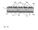
- FIG. 10shows, in the following further course of the process, the residues of doping paste 10 b , produced phosphorus silicate glass PSG 14 b , dielectric masking layer 8 , and AlSi eutectic layer 3 b are etched off in suitable etch baths, so that emitter regions 11 , BSF region 12 , and front-side n + layer 14 are exposed.
- FIG. 11shows both sides are coated by a dielectric in a further method step, e.g., by thermal oxidation of both sides of the wafer in a water vapor atmosphere, so that a silicon oxide layer results on front side 15 a and rear side 15 b.
- FIG. 12shows that the annealing process realized in the manner described leads to excellent surface-passivation results.
- FIG. 13shows passivation layer 15 b is locally removed on the rear side in all emitter and BSF regions, i.e., simultaneously by masked dry etching in a plasma 7 b containing fluorine gas, or without masking by laser ablation, for instance.
- FIG. 14shows, in the following process step, the entire rear side is covered by an aluminum layer 20 , so that all contact surfaces 20 a and 20 b exposed in the preceding etching step are metalized, but otherwise are insulated from the semiconductor regions emitter 11 and BSF 12 by layer 15 b.
- FIG. 15shows that by applying an acid-resistant layer 21 , which may be by structured inkjet-printing, aluminum layer 20 is then subdivided into emitter contact traces and BSF contact traces, and this application is performed so that narrow interspaces 22 a between planned contact regions 22 b are left free, in which the aluminum is removed by an acid 23 that etches aluminum selectively, that is to say, does not attack silicon oxide.
- an acid-resistant layer 21which may be by structured inkjet-printing
- FIG. 16shows, in a supplementary process step, an anti-reflection layer 24 , which may be of silicon nitride, is formed on the front side.
- FIG. 17shows all contacts on the rear side may simultaneously and additionally be provided with a thick metallic conductive layer in a chemical or galvanic bath 25 or with the aid of a possibly light-based deposition process.
- FIG. 18shows, after rinsing and drying the wafer, the back-contacted solar cell is functional.
- n-silicon wafer 1which is untextured in the illustrated example, is covered by an aluminum or aluminum-containing layer 3 , which forms the emitter dopant.
- the front side of the waferis denoted by reference numeral 2 a
- the rear sideby reference numeral 2 b.
- aluminum-containing layer 3is brought into contact with a shadow mask 5 a and structured by a dry-etching step in plasma 7 a containing chlorine gas (cf. FIGS. 2 and 3 ).
- an organic mask layermay be applied as well, e.g., by so-called ink-jetting, and the aluminum in the regions that have remained free then be etched in a wet-chemical manner.
- the two discussed technological variantsproduce longitudinal openings 4 in the form of strips in the region of breakthroughs 6 a of mask 5 a.
- the BSF doping materialis diffused into strip-shaped openings 4 in aluminum layer 3 at a lateral distance to the aluminum edge.
- a further process step according to the exemplary embodiments and/or exemplary methods of the present inventionthen pertains to the coating of the strip-shaped, structured, aluminum-containing layer 3 by a dielectric layer 8 (cf. FIG. 4 ).
- Dielectric layer 8may be made from an oxide, e.g., SiO 2 , TiO 2 , or Al 2 O 3 .
- layer 8may be formed by reactive sputtering or by a CVD- or PECVD method.
- dielectric layer 8is then removed by a masked etching step in the region of openings 6 b of an additional mask 5 b according to FIG. 5 .
- Thismay be a dry-etching step in a plasma 7 b containing fluorine gas, penetrating a metal foil mask, or by a dry-etching step in a plasma atmosphere containing fluorine gas, penetrating an organic mask layer, or a wet-chemical etching process, penetrating an organic mask layer.
- the strip-shaped openings 6 b in mask 5 b and the resulting strip-shaped regions 9 exposed in dielectric layer 8are smaller than the strip-shaped openings 6 a in mask 5 a , and thus in aluminum-containing layer 3 .
- standard-type texturingis then implemented by dipping in a bath of KOH and isopropyl alcohol (IPA), for example. Since aluminum-containing layer 3 is protected by dielectric layer 8 , the texturing in the desired manner takes place only on front side 2 a of the wafer and in the exposed strip-shaped regions 9 b on the rear side of the wafer.
- IPAisopropyl alcohol
- openings 9 in cover layer 8 in the openings of emitter layer 4are covered by a material having a large phosphorus component, which may be a paste, which is able to be deposited on the surface of wafer 1 in local deposits 10 by screen printing, stencil printing or ink-jetting, for example. If necessary, this paste is subjected to a drying step at temperatures of 150° C. to 200° C., for example.
- a material having a large phosphorus componentwhich may be a paste, which is able to be deposited on the surface of wafer 1 in local deposits 10 by screen printing, stencil printing or ink-jetting, for example. If necessary, this paste is subjected to a drying step at temperatures of 150° C. to 200° C., for example.
- a one-step, or optionally a two-step, thermal treatmenttakes place with the possibility of a co-diffusion of the emitter dopant aluminum and the BSF doping material phosphorus from the dried, phosphorus-containing layer 10 b.
- a first thermal treatment steptakes place at temperatures ranging from 900° C. to 1100° C. in a nitrogen-oxygen mixture, which causes the desired co-diffusion ( FIG. 8 ).
- a second treatment stepoptionally takes place at temperatures between 800° C. and 1000° C., i.e., in a phosphorus-containing gas 13 , which may be POCl 3 .
- the first high-temperature stepcauses an interdiffusion of silicon and aluminum and leads to a near-surface, mixed crystal layer 3 b having an eutectic AlSi structure and the p + -doping layer with Al profile 11 .
- the phosphorus from precursor deposit 10 bdiffuses into BSF regions 9 b , into the silicon surface, and leads to a deep n ++ doping 12 .
- the diffusion profile of the phosphorusDue to the high temperatures of >1000° C. required for the aluminum diffusion, the diffusion profile of the phosphorus has a deeper characteristic than in P-diffusion processes around 900° C. that are otherwise the norm.
- the optional second thermal treatment step at said usually lower temperatures, only this time using the POCl 3 atmosphere according to FIG. 9brings about not only the deep P-diffusion in the BSF regions of rear side 9 b , but additionally a flat P-diffusion on front side 2 a , which forms an FSF layer (front surface field) 14 having a layer resistance that is adjustable via the temperature and time, i.e., which may be high layer resistance.
- the first thermal treatment stepmay also be performed prior to the step of coating with the phosphorus-containing paste and independently of the subsequent second thermal treatment step.
- one advantageresults from the fact that the process parameters of the second diffusion step at a lower temperature are able to be optimized, regardless of the process parameters of the first diffusion step at a higher temperature.
- the additional flat diffusion in the phosphorus-containing gas atmospherewhich may be by using POCl 3 , may also be omitted if no front surface field layer 14 is desired as front-side passivation.
- this passivationcould also be performed in an additional third diffusion process, in particular if the first phosphorus diffusion step has also been realized using POCl 3 .
- the residues of doping paste 10 b , produced phosphorus silicate glass PSG 14 b , dielectric masking layer 8 , and AlSi eutectic layer 3 bare etched off in suitable etch baths, so that emitter regions 11 , BSF region 12 , and front-side n + layer 14 are exposed, i.e., according to FIG. 10 .
- both sidesare coated by a dielectric in a further method step, e.g., by thermal oxidation of both sides of the wafer in a water vapor atmosphere, so that a silicon oxide layer results on front side 15 a and rear side 15 b.
- both sideswith a thin aluminum layer once a thermal oxide has formed on both wafer surfaces.
- the layer thicknessmay amount to a range between 10 nm and 100 nm.
- An aluminum layer 16 asubsequently results on the front side, and an aluminum layer 16 b on the rear side.
- the wafers, coated in this way,are then subjected to a thermal treatment at a range between 350° C. and 450° C.
- the annealing process realized in this mannerleads to excellent surface-passivation results (cf. FIG. 12 ).
- the waferis once again in a state as shown in FIG. 11 .
- passivation layer 15 bis locally removed on the rear side in all emitter and BSF regions, i.e., simultaneously by masked dry etching in a plasma 7 b containing fluorine gas, or without masking by laser ablation, for instance.
- the generally known LFC methodmay be used once the base metal coating has been deposited.
- Openings 18 a above emitter regions 11 , and openings 18 b above the BSF regions in mask 17are smaller than openings 6 b in mask 5 b of the preceding etching step.
- thisfacilitates the adjustment of the shadow mask or mask layer 17 on the already existing structure; for another, the contact regions of the metallization to the semiconductor material are to be small, if possible, in order to restrict the surface recombination.
- the entire rear sideis covered by an aluminum layer 20 , so that all contact surfaces 20 a and 20 b exposed in the preceding etching step are metalized, but otherwise are insulated from the semiconductor regions emitter 11 and BSF 12 by layer 15 b (cf. FIG. 14 ).
- an acid-resistant layer 21which may be by structured inkjet-printing
- aluminum layer 20is then subdivided into emitter contact traces and BSF contact traces.
- This applicationis performed in such a way that narrow interspaces 22 a between planned contact regions 22 b are left free, in which the aluminum is removed by an acid 23 that etches aluminum selectively, that is to say, does not attack silicon oxide (cf. FIG. 15 ).
- an organic pasteis used which dries on the surface, or a hot-melt wax is used, which is injected while warm and then solidifies on the wafer while cooling.
- suitable inkwhich is subjected to a drying process.
- an anti-reflection layer 24which may be of silicon nitride, is formed on the front side. With regard to thickness and refractive index, this anti-reflection layer is developed with a view toward optimum efficiency with respect to trapping energy from sunlight. Plasma-aided CVD or reactive sputtering, for instance, may be used to deposit this anti-reflection layer 24 .
- the plasma CVD methodis used for this purpose because it takes place at temperatures above 400° C. yet below 500° C. and therefore causes annealing of aluminum contact layer 20 and thus a reduction in the contact resistance, without risking an AlSi liquefaction at the eutectic temperature of 577° C.
- all contacts on the rear sidemay simultaneously and additionally be provided with a thick metallic conductive layer in a chemical or galvanic bath 25 or with the aid of a possibly light-based deposition process.
- the individual layersmay either consist of a single material of nickel, copper or silver, or of a plurality of individual layers of different metals, such as Ni+Cu+Sn or Ni+Ag or Ni+Au, for example.
- the back-contacted solar cellAfter rinsing and drying the wafer, the back-contacted solar cell is functional, as shown in FIG. 18 .
- An edge insulationis not required since the lateral clearance and the oxide cover ensure the separation of emitter regions 11 and BSF regions.
Landscapes
- Photovoltaic Devices (AREA)
- Electrodes Of Semiconductors (AREA)
- Life Sciences & Earth Sciences (AREA)
- Chemical & Material Sciences (AREA)
- Crystallography & Structural Chemistry (AREA)
- Sustainable Development (AREA)
Abstract
Description
- The present invention relates to a method for producing monocrystalline n-silicon solar cells having a p+ emitter on the rear side and spatially separate, heavily doped n++ base regions near the surface on the rear side, as well as an interdigitated rear-side contact finger structure, which is in conductive contact with the p+ emitter regions and the n++ base regions, and it also relates to a solar cell produced according to such a method.
- Back contact solar cells on monocrystalline n-Si wafers have been developed by different solar cell manufacturers for a number of years, and some of these cells are already available on the market.
- For example, reference is made to the so-called A300 cell by SunPower (cf. W. D. Mulligan, D. H. Rose, M. J. Cudzinovic, D. M. DeCeuster, K. R. McIntosh, D. D. Smith, R. M. Swanson, “Manufacture of solar cells with 21% efficiency”, Proceedings of the 19th European Photovoltaic Solar Energy Conference, Paris, France (2004)). The A300 cell is a so-called interdigitated back contact cell (IBC), which means that both the emitter and the BSF (back surface field) or base contact strips are situated on the rear side of the cell and are developed in the form of two meshing fork structures.
- The required electrical separation of adjacently located n-doped and p-doped semiconductor regions on the same surface may be achieved in different ways. For example, there is the possibility of placing the two regions at different levels by removing the silicon oxide precipitated on the rear surface around the regions provided as base contacts using laser ablation (P. Engelhardt, N. -P. Harder, T. Neubert, H. Plagwitz, B. Fischer, R. Meyer and R. Brendel, “Laser Processing of 22% Efficient Back-Contacted Silicon Solar Cells”, 21st European Photovoltaic Solar Energy Conference, Dresden, 2006, p. 1).
- Once the surface damage caused by the laser process, and approx. 20 μm of the silicon have been removed by wet-chemical etching, the emitter doping with phosphorus into the deeper-lying regions of the rear side, the front side and the connecting holes between front emitter and rear side emitter is implemented simultaneously, with the aid of a standard POCl3process.
- The metallic coating of both regions then takes place in a single aluminum vapor deposit step, the contact regions being electrically separated from each other by tearing the thin metal layer at the produced, virtually perpendicular step structure in the semiconductor surface.
- Technologies for the production of passivated emitters and of local spot contacts to the two semiconductor regions of base and emitter are likewise known and acknowledged in the literature (cf. R. A. Sinton, Y. Kwark, R. M. Swanson, “Recombination Mechanisms in Silicon Solar Cells”, 14th Project Integration Meeting, Photovoltaic Concentrator Technology Project, June 1986, p. 117-125).
- The local opening of the passivation layer, which simultaneously is the insulation between the semiconductor regions and the superposed metallic current paths, is increasingly implemented with the aid of lasers. On the one hand, so-called laser ablation is employed for removing the insulation layer only locally. On the other hand, the so-called laser-fired contact method (LFC) is employed, in which laser flashes move the vapor-deposited or sputtered aluminum layer through the insulating layer in order to contact the semiconductor regions lying underneath.
- From DE 696 31 815 T2, it is known to use an AlSi eutecticum as conductor base for the p-emitter structure, which is produced on the surface once the aluminum has diffused into the silicon through a previously inwardly diffused n+ layer of the rear side. The solution there also uses screen printing of aluminum paste through oxide windows above the n-base regions. The disadvantage of this solution is that the aluminum doping and the contacting of the aluminum emitter must be implemented in one step, i.e., across a large surface, so that the surface of the emitter and the surface of the metal contacting are identical. Thus, no passivation of the emitter with local contacts is possible. This results in a large surface recombination rate and thus relatively low efficiency.
- Both the laser ablation and the LFC method for the production of local contacts have the disadvantage that these methods are of sequential nature. In other words, the holes for each wafer must be produced individually, one after the other.
- In view of the above, it therefore is an object of the exemplary embodiments and/or exemplary methods of the present invention to provide a further developed method for producing monocrystalline n-silicon solar cells having rear-side, passivated p+ emitters and spatially separate, heavily doped n++ base regions near the surface, as well as an interdigitated rear-side contact finger structure, which allows high productivity and avoids the disadvantages of the related art.
- Furthermore, it should be possible to combine technological steps, particularly steps that cost considerable time in the production process, in order to ensure a further improvement in productivity.
- Furthermore, the use of wafer-protecting technologies known from the production of microelectronics chips, such as sputtering, vapor deposition, CVD, masked dry-etching of aluminum and of oxides using different halogen plasmas, as well as ink-jetting are to be made available for the production of solar cells.
- According to the exemplary embodiments and/or exemplary methods of the present invention, for the method this objective is achieved by the features described herein, and with regard to the solar cell, it is achieved by a subject matter according to the feature combination as further described herein, the further embodiments representing at least useful specific developments and further improvements.
- An important aspect as to the exemplary embodiments and/or exemplary methods of the present invention is the production of a rear-side, locally diffused and passivated aluminum emitter and the possibility of carrying out simultaneous two-sided and local n+ doping of n-silicon in the rear-side and front-side n-base regions near the surface. According to the exemplary embodiments and/or exemplary methods of the present invention, the diffusion steps for the emitters and the BSF or FSF region to be produced may be carried out in a common thermal treatment step for the diffusion of the selected emitter doping material of aluminum and the selected BSF/FSF dopant of phosphorus.
- The wafer may already be textured on one side before the aluminum-containing starting layer for the emitter doping is deposited and structured. However, it is also quite possible to carry out the texturing of the wafer only after the aluminum has been deposited and coated with an etch-resistant oxide on the rear side, so that the emitter, and thus the largest part of the rear side, remains untextured.
- As for the rest, the exemplary embodiments and/or exemplary methods of the present invention also shows the process sequence leading up to the finished rear-contacted solar cell, i.e., including the passivation of the front and back sides as well as the production of the contact structure, including the chemical or galvanic reinforcement.
- Essential for the exemplary embodiments and/or exemplary methods of the present invention is also the lateral separation of the emitter and base doping materials embodied in the finished solar cell, and thus the cell production technology, which is novel for solar cells.
- The basis of the method according to the present invention is the deposition of an aluminum or aluminum-containing thin layer on the rear side of the n-silicon wafer as well as the subsequent structuring of this thin layer, through which openings are obtained in the region of the future base contacts. In a further process step, the aluminum is then diffused into the n-silicon wafer in order to form a structured emitter layer. Thus, the aluminum or aluminum-containing layer is structured before being diffused into the wafer itself.
- The mentioned aluminum thin layer may be deposited on the wafer by a vapor-deposition or sputter process.
- The structuring of the deposited aluminum thin layer is performed in the form of strips, which may be by selective etching. Toward this end, dry-etching methods via a metal shadow mask may be employed, but the use of an organic mask is possible as well. Wet-chemical etching may of course be performed as well or selective etching using local printing of an etching paste.
- In a further method step, the structured emitter layer is covered by a dielectric protective layer across the entire surface. Furthermore, this protective layer is opened up in future base doping regions, which may again be realized by etching or with the aid of an etching mask.
- Then, the silicon wafer is subjected to texturing, which takes place on the front side of the wafer and in the region of the openings in the dielectric protective layer.
- These openings may be formed via a strip-etching mask, the width of the produced openings being smaller than the width of the strip-shaped regions in the aluminum-free wafer.
- Material having high phosphorus content is deposited in the region of the openings in the dielectric protective layer in order to produce the heavily doped n++ BSF base regions near the surface.
- This deposition may also be implemented by applying a paste using screen printing or stencil printing, by ink-jetting in local deposits or by similar methods.
- If necessary, the applied paste is subjected to a drying step.
- The BSF doping material is then diffused in a thermal treatment step consisting of one step or multiple steps.
- The diffusing of the aluminum as emitter dopant and the diffusing of the BSF doping material may be performed in a common treatment step in an especially economic process.
- A flat phosphorus diffusion layer (FSF—front surface field) on the front side of the wafer in the region of the openings in the dielectric protective layer may be produced by an additional thermal treatment in a phosphorus-containing atmosphere, in particular a POCl3atmosphere, which has a layer resistance that is adjustable via the treatment temperature and the treatment time.
- With the aid of an etch bath, residual doping material, produced phosphorus silicate glass, residue from the insulation layer as well as produced AlSi eutecticum layers are removed, so that the emitter regions, the BSF region, and the possibly existing front-side n+-FSF structure are exposed.
- Subsequently, the wafer is covered by a passivation layer, e.g., a silicon oxide layer. The passivation layer is then locally removed in the emitter regions and the BSF regions on the rear side of the wafer. The entire rear side of the wafer is then covered by a conductive layer, especially an aluminum layer. This conductive layer is used to form the interdigitated contact-finger structure.
- A new type of solar cell is obtained as a result of the briefly outlined method, the n++ base regions on the wafer's rear side having a lateral clearance from the p+-emitter regions, and at least the n++-base regions having a concentration of the emitter doping material that lies below the n-base concentration of the initial wafer.
- The exemplary embodiments and/or exemplary methods of the present invention will be explained in greater detail in the following text with the aid of an exemplary embodiment, using schematic illustrations of the individual process steps.
FIG. 1 shows in a first method step, an entirerear side 2bof n-silicon wafer 1, which is untextured in the illustrated example, is covered by an aluminum or aluminum-containinglayer 3, which forms the emitter dopant.FIG. 2 shows aluminum-containinglayer 3 is brought into contact with ashadow mask 5a.FIG. 3 shows a dry-etching step inplasma 7acontaining chlorine gas.FIG. 4 shows a further process step according to the present invention that pertains to the coating of the strip-shaped, structured, aluminum-containinglayer 3 by adielectric layer 8.FIG. 5 shows, in a further method step,dielectric layer 8 is then removed by a masked etching step in the region ofopenings 6bof anadditional mask 5b.FIG. 6 shows standard-type texturing is then implemented by dipping in a bath of KOH and isopropyl alcohol (IPA).FIG. 7 andFIG. 8 show a first thermal treatment step takes place at temperatures ranging from 900° C. to 1100° C. in a nitrogen-oxygen mixture, which causes the desired co-diffusion.FIG. 9 shows an optional second thermal treatment step at said usually lower temperatures, only this time using the POCl3atmosphere.FIG. 10 shows, in the following further course of the process, the residues ofdoping paste 10b, produced phosphorussilicate glass PSG 14b,dielectric masking layer 8, and AlSieutectic layer 3bare etched off in suitable etch baths, so thatemitter regions 11,BSF region 12, and front-side n+ layer14 are exposed.FIG. 11 shows both sides are coated by a dielectric in a further method step, e.g., by thermal oxidation of both sides of the wafer in a water vapor atmosphere, so that a silicon oxide layer results onfront side 15aandrear side 15b.FIG. 12 shows that the annealing process realized in the manner described leads to excellent surface-passivation results.FIG. 13 shows passivation layer 15bis locally removed on the rear side in all emitter and BSF regions, i.e., simultaneously by masked dry etching in aplasma 7bcontaining fluorine gas, or without masking by laser ablation, for instance.FIG. 14 shows, in the following process step, the entire rear side is covered by analuminum layer 20, so that all contact surfaces20aand20bexposed in the preceding etching step are metalized, but otherwise are insulated from thesemiconductor regions emitter 11 andBSF 12 bylayer 15b.FIG. 15 shows that by applying an acid-resistant layer 21, which may be by structured inkjet-printing,aluminum layer 20 is then subdivided into emitter contact traces and BSF contact traces, and this application is performed so thatnarrow interspaces 22abetweenplanned contact regions 22bare left free, in which the aluminum is removed by anacid 23 that etches aluminum selectively, that is to say, does not attack silicon oxide.FIG. 16 shows, in a supplementary process step, ananti-reflection layer 24, which may be of silicon nitride, is formed on the front side.FIG. 17 shows all contacts on the rear side may simultaneously and additionally be provided with a thick metallic conductive layer in a chemical orgalvanic bath 25 or with the aid of a possibly light-based deposition process.FIG. 18 shows, after rinsing and drying the wafer, the back-contacted solar cell is functional.- In a first method step according to
FIG. 1 , entirerear side 2bof n-silicon wafer 1, which is untextured in the illustrated example, is covered by an aluminum or aluminum-containinglayer 3, which forms the emitter dopant. The front side of the wafer is denoted byreference numeral 2a, and the rear side byreference numeral 2b. - In a further step, aluminum-containing
layer 3 is brought into contact with ashadow mask 5aand structured by a dry-etching step inplasma 7acontaining chlorine gas (cf.FIGS. 2 and 3 ). - As an alternative, an organic mask layer may be applied as well, e.g., by so-called ink-jetting, and the aluminum in the regions that have remained free then be etched in a wet-chemical manner.
- The two discussed technological variants produce
longitudinal openings 4 in the form of strips in the region ofbreakthroughs 6aofmask 5a. - At a later point, the BSF doping material is diffused into strip-shaped
openings 4 inaluminum layer 3 at a lateral distance to the aluminum edge. - A further process step according to the exemplary embodiments and/or exemplary methods of the present invention then pertains to the coating of the strip-shaped, structured, aluminum-containing
layer 3 by a dielectric layer8 (cf.FIG. 4 ).Dielectric layer 8 may be made from an oxide, e.g., SiO2, TiO2, or Al2O3. - It is also possible to form a silicon nitride layer, which likewise is impermeable to phosphorus diffusion. The deposition of
layer 8 may be performed by reactive sputtering or by a CVD- or PECVD method. - In a further method step,
dielectric layer 8 is then removed by a masked etching step in the region ofopenings 6bof anadditional mask 5baccording toFIG. 5 . - This may be a dry-etching step in a
plasma 7bcontaining fluorine gas, penetrating a metal foil mask, or by a dry-etching step in a plasma atmosphere containing fluorine gas, penetrating an organic mask layer, or a wet-chemical etching process, penetrating an organic mask layer. - According to the exemplary embodiments and/or exemplary methods of the present invention, the strip-shaped
openings 6binmask 5band the resulting strip-shapedregions 9 exposed indielectric layer 8 are smaller than the strip-shapedopenings 6ainmask 5a, and thus in aluminum-containinglayer 3. - This prevents the occurrence of a short-circuit between the emitter regions and the BSF regions during the phosphorus doping in the next process step.
- According to the illustration in
FIG. 6 , standard-type texturing is then implemented by dipping in a bath of KOH and isopropyl alcohol (IPA), for example. Since aluminum-containinglayer 3 is protected bydielectric layer 8, the texturing in the desired manner takes place only onfront side 2aof the wafer and in the exposed strip-shapedregions 9bon the rear side of the wafer. - Subsequently,
openings 9 incover layer 8 in the openings ofemitter layer 4 are covered by a material having a large phosphorus component, which may be a paste, which is able to be deposited on the surface ofwafer 1 inlocal deposits 10 by screen printing, stencil printing or ink-jetting, for example. If necessary, this paste is subjected to a drying step at temperatures of 150° C. to 200° C., for example. - According to the illustrations in
FIGS. 8 and 9 , a one-step, or optionally a two-step, thermal treatment takes place with the possibility of a co-diffusion of the emitter dopant aluminum and the BSF doping material phosphorus from the dried, phosphorus-containinglayer 10b. - A first thermal treatment step takes place at temperatures ranging from 900° C. to 1100° C. in a nitrogen-oxygen mixture, which causes the desired co-diffusion (
FIG. 8 ). A second treatment step optionally takes place at temperatures between 800° C. and 1000° C., i.e., in a phosphorus-containinggas 13, which may be POCl3. - The first high-temperature step causes an interdiffusion of silicon and aluminum and leads to a near-surface,
mixed crystal layer 3bhaving an eutectic AlSi structure and the p+-doping layer withAl profile 11. - At the same time, the phosphorus from
precursor deposit 10bdiffuses intoBSF regions 9b, into the silicon surface, and leads to a deep n++ doping12. - Due to the high temperatures of >1000° C. required for the aluminum diffusion, the diffusion profile of the phosphorus has a deeper characteristic than in P-diffusion processes around 900° C. that are otherwise the norm.
- The optional second thermal treatment step at said usually lower temperatures, only this time using the POCl3atmosphere according to
FIG. 9 , brings about not only the deep P-diffusion in the BSF regions ofrear side 9b, but additionally a flat P-diffusion onfront side 2a, which forms an FSF layer (front surface field)14 having a layer resistance that is adjustable via the temperature and time, i.e., which may be high layer resistance. - Of course, the first thermal treatment step may also be performed prior to the step of coating with the phosphorus-containing paste and independently of the subsequent second thermal treatment step. In this case one advantage results from the fact that the process parameters of the second diffusion step at a lower temperature are able to be optimized, regardless of the process parameters of the first diffusion step at a higher temperature.
- In the same way, the additional flat diffusion in the phosphorus-containing gas atmosphere, which may be by using POCl3, may also be omitted if no front
surface field layer 14 is desired as front-side passivation. On the other hand, this passivation could also be performed in an additional third diffusion process, in particular if the first phosphorus diffusion step has also been realized using POCl3. - In the following further course of the process, the residues of
doping paste 10b, produced phosphorussilicate glass PSG 14b,dielectric masking layer 8, and AlSieutectic layer 3bare etched off in suitable etch baths, so thatemitter regions 11,BSF region 12, and front-side n+ layer14 are exposed, i.e., according toFIG. 10 . - As illustrated in
FIG. 11 , both sides are coated by a dielectric in a further method step, e.g., by thermal oxidation of both sides of the wafer in a water vapor atmosphere, so that a silicon oxide layer results onfront side 15aandrear side 15b. - Optionally, it is possible to coat both sides with a thin aluminum layer once a thermal oxide has formed on both wafer surfaces. The layer thickness may amount to a range between 10 nm and 100 nm. An
aluminum layer 16asubsequently results on the front side, and analuminum layer 16bon the rear side. The wafers, coated in this way, are then subjected to a thermal treatment at a range between 350° C. and 450° C. The annealing process realized in this manner leads to excellent surface-passivation results (cf.FIG. 12 ). - When the aluminum layer has been etched off, the wafer is once again in a state as shown in
FIG. 11 . - Furthermore, as shown in
FIG. 13 ,passivation layer 15bis locally removed on the rear side in all emitter and BSF regions, i.e., simultaneously by masked dry etching in aplasma 7bcontaining fluorine gas, or without masking by laser ablation, for instance. In the same way, the generally known LFC method may be used once the base metal coating has been deposited. Openings 18aabove emitter regions 11, andopenings 18babove the BSF regions inmask 17 are smaller thanopenings 6binmask 5bof the preceding etching step.- For one, this facilitates the adjustment of the shadow mask or
mask layer 17 on the already existing structure; for another, the contact regions of the metallization to the semiconductor material are to be small, if possible, in order to restrict the surface recombination. - In the following process step, the entire rear side is covered by an
aluminum layer 20, so that all contact surfaces20aand20bexposed in the preceding etching step are metalized, but otherwise are insulated from thesemiconductor regions emitter 11 andBSF 12 bylayer 15b(cf.FIG. 14 ). - By applying an acid-
resistant layer 21, which may be by structured inkjet-printing,aluminum layer 20 is then subdivided into emitter contact traces and BSF contact traces. This application is performed in such a way that narrow interspaces22abetweenplanned contact regions 22bare left free, in which the aluminum is removed by anacid 23 that etches aluminum selectively, that is to say, does not attack silicon oxide (cf.FIG. 15 ). During the inkjet printing, either an organic paste is used which dries on the surface, or a hot-melt wax is used, which is injected while warm and then solidifies on the wafer while cooling. Another possibility is the use of suitable ink, which is subjected to a drying process. - In a supplementary process step, as shown in
FIG. 16 , ananti-reflection layer 24, which may be of silicon nitride, is formed on the front side. With regard to thickness and refractive index, this anti-reflection layer is developed with a view toward optimum efficiency with respect to trapping energy from sunlight. Plasma-aided CVD or reactive sputtering, for instance, may be used to deposit thisanti-reflection layer 24. - It is preferred if the plasma CVD method is used for this purpose because it takes place at temperatures above 400° C. yet below 500° C. and therefore causes annealing of
aluminum contact layer 20 and thus a reduction in the contact resistance, without risking an AlSi liquefaction at the eutectic temperature of 577° C. - According to
FIG. 17 , all contacts on the rear side may simultaneously and additionally be provided with a thick metallic conductive layer in a chemical orgalvanic bath 25 or with the aid of a possibly light-based deposition process. This results in the production of emittercircuit trace reinforcements 26aor BSFcircuit trace reinforcements 26b. The individual layers may either consist of a single material of nickel, copper or silver, or of a plurality of individual layers of different metals, such as Ni+Cu+Sn or Ni+Ag or Ni+Au, for example. - After rinsing and drying the wafer, the back-contacted solar cell is functional, as shown in
FIG. 18 . An edge insulation is not required since the lateral clearance and the oxide cover ensure the separation ofemitter regions 11 and BSF regions.
Claims (27)
Applications Claiming Priority (7)
| Application Number | Priority Date | Filing Date | Title |
|---|---|---|---|
| DE102008009268 | 2008-02-15 | ||
| DE102008009268.1 | 2008-02-15 | ||
| DE102008009268 | 2008-02-15 | ||
| DE102008013446.5 | 2008-03-10 | ||
| DE102008013446ADE102008013446A1 (en) | 2008-02-15 | 2008-03-10 | Process for producing monocrystalline n-silicon solar cells and solar cell, produced by such a process |
| DE102008013446 | 2008-03-10 | ||
| PCT/EP2009/051569WO2009101107A1 (en) | 2008-02-15 | 2009-02-11 | Method for the production of monocrystalline n-silicon solar cells, and solar cell produced according to such a method |
Related Parent Applications (1)
| Application Number | Title | Priority Date | Filing Date |
|---|---|---|---|
| PCT/EP2009/051569A-371-Of-InternationalWO2009101107A1 (en) | 2008-02-15 | 2009-02-11 | Method for the production of monocrystalline n-silicon solar cells, and solar cell produced according to such a method |
Related Child Applications (1)
| Application Number | Title | Priority Date | Filing Date |
|---|---|---|---|
| US14/244,476DivisionUS20140209166A1 (en) | 2008-02-15 | 2014-04-03 | Method for producing monocrystalline n-silicon solar cells, as well as a solar cell produced according to such a method |
Publications (2)
| Publication Number | Publication Date |
|---|---|
| US20110041902A1true US20110041902A1 (en) | 2011-02-24 |
| US8728922B2 US8728922B2 (en) | 2014-05-20 |
Family
ID=40896795
Family Applications (2)
| Application Number | Title | Priority Date | Filing Date |
|---|---|---|---|
| US12/735,751Expired - Fee RelatedUS8728922B2 (en) | 2008-02-15 | 2009-02-11 | Method for producing monocrystalline N-silicon solar cells, as well as a solar cell produced according to such a method |
| US14/244,476AbandonedUS20140209166A1 (en) | 2008-02-15 | 2014-04-03 | Method for producing monocrystalline n-silicon solar cells, as well as a solar cell produced according to such a method |
Family Applications After (1)
| Application Number | Title | Priority Date | Filing Date |
|---|---|---|---|
| US14/244,476AbandonedUS20140209166A1 (en) | 2008-02-15 | 2014-04-03 | Method for producing monocrystalline n-silicon solar cells, as well as a solar cell produced according to such a method |
Country Status (7)
| Country | Link |
|---|---|
| US (2) | US8728922B2 (en) |
| EP (1) | EP2250675B1 (en) |
| JP (1) | JP2011512661A (en) |
| KR (1) | KR20100136462A (en) |
| CN (1) | CN102017165A (en) |
| DE (1) | DE102008013446A1 (en) |
| WO (1) | WO2009101107A1 (en) |
Cited By (18)
| Publication number | Priority date | Publication date | Assignee | Title |
|---|---|---|---|---|
| US20110041905A1 (en)* | 2009-08-20 | 2011-02-24 | National Taiwan University | Organic solar cell and method for forming the same |
| US20110056545A1 (en)* | 2009-09-07 | 2011-03-10 | Kwangsun Ji | Solar cell |
| US20110259423A1 (en)* | 2010-04-22 | 2011-10-27 | General Electric Company | Methods for forming back contact electrodes for cadmium telluride photovoltaic cells |
| US20130180585A1 (en)* | 2010-07-30 | 2013-07-18 | Sanyo Electric Co., Ltd. | Method of manufacturing solar cell, and solar cell |
| WO2013163231A1 (en)* | 2012-04-23 | 2013-10-31 | Solexel, Inc. | Resistance component extraction for back contact back junction solar cells |
| WO2013184244A1 (en)* | 2012-04-24 | 2013-12-12 | Solexel, Inc. | Manufacturing methods and structures for large-area thin-film solar cells and other semiconductor devices |
| US8642378B1 (en) | 2012-12-18 | 2014-02-04 | International Business Machines Corporation | Field-effect inter-digitated back contact photovoltaic device |
| WO2014098981A1 (en)* | 2012-12-19 | 2014-06-26 | Sunpower Corporation | Solar cell emitter region fabrication using silicon nano-particles |
| WO2014098982A1 (en)* | 2012-12-18 | 2014-06-26 | Sunpower Corporation | Solar cell emitter region fabrication using n-type doped silicon nano-particles |
| US8946547B2 (en) | 2010-08-05 | 2015-02-03 | Solexel, Inc. | Backplane reinforcement and interconnects for solar cells |
| US8962380B2 (en) | 2009-12-09 | 2015-02-24 | Solexel, Inc. | High-efficiency photovoltaic back-contact solar cell structures and manufacturing methods using thin planar semiconductor absorbers |
| US20150096612A1 (en)* | 2013-10-09 | 2015-04-09 | Neo Solar Power Corp. | Back-contact solar cell and manufacturing method thereof |
| CN104576312A (en)* | 2013-10-29 | 2015-04-29 | 中芯国际集成电路制造(上海)有限公司 | Method for preventing crystal defect from being produced on surface of phosphor-doped silicon oxide film |
| WO2015142554A1 (en)* | 2014-03-20 | 2015-09-24 | Varian Semiconductor Equipment Associates, Inc. | Advanced back contact solar cells |
| US20160027951A1 (en)* | 2014-07-28 | 2016-01-28 | Lg Electronics Inc. | Solar cell and method for manufacturing the same |
| US9263616B2 (en) | 2012-12-06 | 2016-02-16 | International Business Machines Corporation | Selective emitter photovoltaic device |
| US9312405B2 (en) | 2012-03-02 | 2016-04-12 | Intellectual Keystone Technology Llc | Thin film type solar cell and fabrication method thereof |
| EP3050122A4 (en)* | 2013-09-27 | 2016-09-21 | Sunpower Corp | METALLIZING SOLAR CELLS USING METALLIC SHEETS |
Families Citing this family (28)
| Publication number | Priority date | Publication date | Assignee | Title |
|---|---|---|---|---|
| DE102009015764A1 (en)* | 2008-10-31 | 2010-06-17 | Bosch Solar Energy Ag | Process for producing monocrystalline n-silicon back contact solar cells |
| DE102009008786A1 (en)* | 2008-10-31 | 2010-06-10 | Bosch Solar Energy Ag | Process for producing a solar cell and solar cell |
| DE202010018510U1 (en) | 2009-09-07 | 2017-03-15 | Lg Electronics Inc. | solar cell |
| NL2004065C2 (en)* | 2010-01-06 | 2011-07-07 | Stichting Energie | Solar panel module and method for manufacturing such a solar panel module. |
| KR101027829B1 (en)* | 2010-01-18 | 2011-04-07 | 현대중공업 주식회사 | Manufacturing method of back electrode solar cell |
| FR2956242A1 (en)* | 2010-02-05 | 2011-08-12 | Commissariat Energie Atomique | Substrate i.e. P-type silicon substrate, realizing method for forming photovoltaic cell, involves realizing diffusion heat treatment to form first and second volumes doped respectively from sources of dopants |
| DE102010027940A1 (en) | 2010-04-20 | 2011-10-20 | Robert Bosch Gmbh | Process for producing a solar cell and solar cell produced by this process |
| DE102010028187A1 (en)* | 2010-04-26 | 2011-10-27 | Robert Bosch Gmbh | A method of making a metal wrap-through solar cell and a metal wrap-through solar cell made by this method |
| DE102010028189B4 (en) | 2010-04-26 | 2018-09-27 | Solarworld Industries Gmbh | solar cell |
| CN102148283A (en)* | 2010-09-28 | 2011-08-10 | 常州天合光能有限公司 | Method for preparing N-type solar battery by one-step diffusion |
| KR101145472B1 (en)* | 2010-11-29 | 2012-05-15 | 현대중공업 주식회사 | Method for fabricating solar cell |
| US8889981B2 (en) | 2011-10-18 | 2014-11-18 | Samsung Sdi Co., Ltd. | Photoelectric device |
| KR20130050721A (en) | 2011-11-08 | 2013-05-16 | 삼성에스디아이 주식회사 | Solar cell |
| KR101902887B1 (en)* | 2011-12-23 | 2018-10-01 | 엘지전자 주식회사 | Method for manufacturing the same |
| US11038080B2 (en)* | 2012-01-19 | 2021-06-15 | Utica Leaseco, Llc | Thin-film semiconductor optoelectronic device with textured front and/or back surface prepared from etching |
| CN103107237B (en)* | 2012-12-06 | 2016-03-23 | 杭州赛昂电力有限公司 | Monocrystaline silicon solar cell and preparation method thereof |
| US20140158192A1 (en)* | 2012-12-06 | 2014-06-12 | Michael Cudzinovic | Seed layer for solar cell conductive contact |
| US9525082B2 (en)* | 2013-09-27 | 2016-12-20 | Sunpower Corporation | Solar cell contact structures formed from metal paste |
| TWI496299B (en)* | 2013-10-30 | 2015-08-11 | Inventec Solar Energy Corp | Electrode structure and solar cell using electrode structure |
| CN103943726B (en)* | 2014-04-22 | 2016-03-23 | 英利集团有限公司 | Preparation method of N-type solar cell and preparation method of high-low junction |
| KR102219804B1 (en) | 2014-11-04 | 2021-02-24 | 엘지전자 주식회사 | Solar cell and the manufacturing mathod thereof |
| US20170012149A1 (en)* | 2015-07-07 | 2017-01-12 | Crystal Solar, Inc. | High efficiency single crystal silicon solar cell with epitaxially deposited silicon layers with deep junction(s) |
| CN105244392A (en)* | 2015-11-09 | 2016-01-13 | 常州天合光能有限公司 | Photovoltaic cell applied to automobile roof for improving shadow shading reliability, and manufacturing method thereof |
| JP6211743B1 (en)* | 2016-12-13 | 2017-10-11 | 信越化学工業株式会社 | High efficiency back electrode type solar cell, solar cell module, and solar power generation system |
| WO2019195806A2 (en)* | 2018-04-06 | 2019-10-10 | Sunpower Corporation | Local patterning and metallization of semiconductor structures using a laser beam |
| CN110718604A (en)* | 2018-06-26 | 2020-01-21 | 上海硅洋新能源科技有限公司 | P-type crystalline silicon solar cell back field and back passivation layer preparation method |
| IT202300009720A1 (en) | 2023-05-15 | 2024-11-15 | Iinformatica S R L | Triboelectric photovoltaic-pyroelectric cell for the production of clean energy from wind and light irradiation |
| CN117810310B (en)* | 2024-02-29 | 2024-06-07 | 浙江晶科能源有限公司 | Solar cell preparation method, solar cell and photovoltaic module |
Citations (12)
| Publication number | Priority date | Publication date | Assignee | Title |
|---|---|---|---|---|
| US5609775A (en)* | 1995-03-17 | 1997-03-11 | Chartered Semiconductor Manufacturing Pte Ltd. | Dry etch process for titanium-tungsten films |
| US5641362A (en)* | 1995-11-22 | 1997-06-24 | Ebara Solar, Inc. | Structure and fabrication process for an aluminum alloy junction self-aligned back contact silicon solar cell |
| US6262359B1 (en)* | 1999-03-17 | 2001-07-17 | Ebara Solar, Inc. | Aluminum alloy back junction solar cell and a process for fabrication thereof |
| US20020016016A1 (en)* | 2000-06-01 | 2002-02-07 | Kouji Tsuzuki | Process for producing a photovoltaic element |
| US20020172898A1 (en)* | 2001-05-17 | 2002-11-21 | Honeywell International Inc. | Layered hard mask and dielectric materials and methods therefor |
| US6593224B1 (en)* | 2002-03-05 | 2003-07-15 | Bridge Semiconductor Corporation | Method of manufacturing a multilayer interconnect substrate |
| US6825104B2 (en)* | 1996-12-24 | 2004-11-30 | Interuniversitair Micro-Elektronica Centrum (Imec) | Semiconductor device with selectively diffused regions |
| US20050172996A1 (en)* | 2004-02-05 | 2005-08-11 | Advent Solar, Inc. | Contact fabrication of emitter wrap-through back contact silicon solar cells |
| US6998288B1 (en)* | 2003-10-03 | 2006-02-14 | Sunpower Corporation | Use of doped silicon dioxide in the fabrication of solar cells |
| US20060148233A1 (en)* | 2001-09-21 | 2006-07-06 | Madhav Datta | Copper-containing C4 ball-limiting metallurgy stack for enhanced reliability of packaged structures and method of making same |
| US20060275936A1 (en)* | 2003-04-29 | 2006-12-07 | Pierre-Jean Ribeyron | Method for production of a semiconductor device with auto-aligned metallisations |
| US7807556B2 (en)* | 2006-12-05 | 2010-10-05 | General Electric Company | Method for doping impurities |
Family Cites Families (14)
| Publication number | Priority date | Publication date | Assignee | Title |
|---|---|---|---|---|
| US4478879A (en)* | 1983-02-10 | 1984-10-23 | The United States Of America As Represented By The Administrator Of The National Aeronautics And Space Administration | Screen printed interdigitated back contact solar cell |
| JPH03285360A (en)* | 1990-03-31 | 1991-12-16 | Mitsubishi Materials Corp | Solar cell |
| ES2090745T3 (en)* | 1992-04-28 | 1996-10-16 | Siemens Solar Gmbh | SEMICONDUCTOR BODY WITH WELL-STICK METALLIZATION. |
| JP3368145B2 (en)* | 1996-06-20 | 2003-01-20 | シャープ株式会社 | Method of manufacturing solar cell |
| US6180869B1 (en) | 1997-05-06 | 2001-01-30 | Ebara Solar, Inc. | Method and apparatus for self-doping negative and positive electrodes for silicon solar cells and other devices |
| JP2000138386A (en) | 1998-11-04 | 2000-05-16 | Shin Etsu Chem Co Ltd | Solar cell manufacturing method and solar cell manufactured by this method |
| JP3300812B2 (en)* | 2000-01-19 | 2002-07-08 | 独立行政法人産業技術総合研究所 | Photoelectric conversion element |
| DE10021440A1 (en) | 2000-05-03 | 2001-11-15 | Univ Konstanz | Process for producing a solar cell and solar cell produced by this process |
| US7388147B2 (en)* | 2003-04-10 | 2008-06-17 | Sunpower Corporation | Metal contact structure for solar cell and method of manufacture |
| JP2005150614A (en)* | 2003-11-19 | 2005-06-09 | Sharp Corp | Solar cell and manufacturing method thereof |
| EP1763086A1 (en)* | 2005-09-09 | 2007-03-14 | Interuniversitair Micro-Elektronica Centrum | Photovoltaic cell with thick silicon oxide and silicon nitride passivation and fabrication method |
| US20070137692A1 (en)* | 2005-12-16 | 2007-06-21 | Bp Corporation North America Inc. | Back-Contact Photovoltaic Cells |
| JP2007281044A (en) | 2006-04-04 | 2007-10-25 | Canon Inc | Solar cell |
| US20080072953A1 (en)* | 2006-09-27 | 2008-03-27 | Thinsilicon Corp. | Back contact device for photovoltaic cells and method of manufacturing a back contact device |
- 2008
- 2008-03-10DEDE102008013446Apatent/DE102008013446A1/ennot_activeWithdrawn
- 2009
- 2009-02-11EPEP09711197.5Apatent/EP2250675B1/ennot_activeNot-in-force
- 2009-02-11USUS12/735,751patent/US8728922B2/ennot_activeExpired - Fee Related
- 2009-02-11CNCN2009801134617Apatent/CN102017165A/enactivePending
- 2009-02-11KRKR1020107020690Apatent/KR20100136462A/ennot_activeCeased
- 2009-02-11WOPCT/EP2009/051569patent/WO2009101107A1/enactiveApplication Filing
- 2009-02-11JPJP2010546320Apatent/JP2011512661A/enactivePending
- 2014
- 2014-04-03USUS14/244,476patent/US20140209166A1/ennot_activeAbandoned
Patent Citations (13)
| Publication number | Priority date | Publication date | Assignee | Title |
|---|---|---|---|---|
| US5609775A (en)* | 1995-03-17 | 1997-03-11 | Chartered Semiconductor Manufacturing Pte Ltd. | Dry etch process for titanium-tungsten films |
| US5641362A (en)* | 1995-11-22 | 1997-06-24 | Ebara Solar, Inc. | Structure and fabrication process for an aluminum alloy junction self-aligned back contact silicon solar cell |
| US6825104B2 (en)* | 1996-12-24 | 2004-11-30 | Interuniversitair Micro-Elektronica Centrum (Imec) | Semiconductor device with selectively diffused regions |
| US6262359B1 (en)* | 1999-03-17 | 2001-07-17 | Ebara Solar, Inc. | Aluminum alloy back junction solar cell and a process for fabrication thereof |
| US20020016016A1 (en)* | 2000-06-01 | 2002-02-07 | Kouji Tsuzuki | Process for producing a photovoltaic element |
| US20020172898A1 (en)* | 2001-05-17 | 2002-11-21 | Honeywell International Inc. | Layered hard mask and dielectric materials and methods therefor |
| US20060148233A1 (en)* | 2001-09-21 | 2006-07-06 | Madhav Datta | Copper-containing C4 ball-limiting metallurgy stack for enhanced reliability of packaged structures and method of making same |
| US6593224B1 (en)* | 2002-03-05 | 2003-07-15 | Bridge Semiconductor Corporation | Method of manufacturing a multilayer interconnect substrate |
| US20060275936A1 (en)* | 2003-04-29 | 2006-12-07 | Pierre-Jean Ribeyron | Method for production of a semiconductor device with auto-aligned metallisations |
| US6998288B1 (en)* | 2003-10-03 | 2006-02-14 | Sunpower Corporation | Use of doped silicon dioxide in the fabrication of solar cells |
| US7135350B1 (en)* | 2003-10-03 | 2006-11-14 | Sunpower Corporation | Use of doped silicon dioxide in the fabrication of solar cells |
| US20050172996A1 (en)* | 2004-02-05 | 2005-08-11 | Advent Solar, Inc. | Contact fabrication of emitter wrap-through back contact silicon solar cells |
| US7807556B2 (en)* | 2006-12-05 | 2010-10-05 | General Electric Company | Method for doping impurities |
Cited By (33)
| Publication number | Priority date | Publication date | Assignee | Title |
|---|---|---|---|---|
| US20110041905A1 (en)* | 2009-08-20 | 2011-02-24 | National Taiwan University | Organic solar cell and method for forming the same |
| USRE47484E1 (en) | 2009-09-07 | 2019-07-02 | Lg Electronics Inc. | Solar cell |
| US8525018B2 (en) | 2009-09-07 | 2013-09-03 | Lg Electronics Inc. | Solar cell |
| US20110056545A1 (en)* | 2009-09-07 | 2011-03-10 | Kwangsun Ji | Solar cell |
| USRE46515E1 (en) | 2009-09-07 | 2017-08-15 | Lg Electronics Inc. | Solar cell |
| US8962380B2 (en) | 2009-12-09 | 2015-02-24 | Solexel, Inc. | High-efficiency photovoltaic back-contact solar cell structures and manufacturing methods using thin planar semiconductor absorbers |
| US8524524B2 (en)* | 2010-04-22 | 2013-09-03 | General Electric Company | Methods for forming back contact electrodes for cadmium telluride photovoltaic cells |
| US9054241B2 (en) | 2010-04-22 | 2015-06-09 | First Solar, Inc. | Back contact electrodes for cadmium telluride photovoltaic cells |
| US20110259423A1 (en)* | 2010-04-22 | 2011-10-27 | General Electric Company | Methods for forming back contact electrodes for cadmium telluride photovoltaic cells |
| US20130180585A1 (en)* | 2010-07-30 | 2013-07-18 | Sanyo Electric Co., Ltd. | Method of manufacturing solar cell, and solar cell |
| US10134940B2 (en)* | 2010-07-30 | 2018-11-20 | Panasonic Intellectual Property Management Co., Ltd. | Method of manufacturing solar cell |
| US8946547B2 (en) | 2010-08-05 | 2015-02-03 | Solexel, Inc. | Backplane reinforcement and interconnects for solar cells |
| US9312405B2 (en) | 2012-03-02 | 2016-04-12 | Intellectual Keystone Technology Llc | Thin film type solar cell and fabrication method thereof |
| WO2013163231A1 (en)* | 2012-04-23 | 2013-10-31 | Solexel, Inc. | Resistance component extraction for back contact back junction solar cells |
| WO2013184244A1 (en)* | 2012-04-24 | 2013-12-12 | Solexel, Inc. | Manufacturing methods and structures for large-area thin-film solar cells and other semiconductor devices |
| US9263616B2 (en) | 2012-12-06 | 2016-02-16 | International Business Machines Corporation | Selective emitter photovoltaic device |
| WO2014098982A1 (en)* | 2012-12-18 | 2014-06-26 | Sunpower Corporation | Solar cell emitter region fabrication using n-type doped silicon nano-particles |
| US8829339B2 (en) | 2012-12-18 | 2014-09-09 | International Business Machines Corporation | Field-effect inter-digitated back contact photovoltaic device |
| US8642378B1 (en) | 2012-12-18 | 2014-02-04 | International Business Machines Corporation | Field-effect inter-digitated back contact photovoltaic device |
| WO2014098981A1 (en)* | 2012-12-19 | 2014-06-26 | Sunpower Corporation | Solar cell emitter region fabrication using silicon nano-particles |
| US9559246B2 (en) | 2012-12-19 | 2017-01-31 | Sunpower Corporation | Solar cell emitter region fabrication using silicon nano-particles |
| US8785233B2 (en) | 2012-12-19 | 2014-07-22 | Sunpower Corporation | Solar cell emitter region fabrication using silicon nano-particles |
| US9252319B2 (en) | 2012-12-19 | 2016-02-02 | Sunpower Corporation | Solar cell emitter region fabrication using silicon nano-particles |
| EP3050122A4 (en)* | 2013-09-27 | 2016-09-21 | Sunpower Corp | METALLIZING SOLAR CELLS USING METALLIC SHEETS |
| US9865753B2 (en) | 2013-09-27 | 2018-01-09 | Sunpower Corporation | Metallization of solar cells using metal foils |
| CN108039380A (en)* | 2013-09-27 | 2018-05-15 | 太阳能公司 | Solar cell is metallized using metal foil |
| AU2014327036B2 (en)* | 2013-09-27 | 2018-07-05 | Maxeon Solar Pte. Ltd. | Metallization of solar cells using metal foils |
| CN104576822A (en)* | 2013-10-09 | 2015-04-29 | 新日光能源科技股份有限公司 | Back contact solar cell and method for manufacturing the same |
| US20150096612A1 (en)* | 2013-10-09 | 2015-04-09 | Neo Solar Power Corp. | Back-contact solar cell and manufacturing method thereof |
| CN104576312A (en)* | 2013-10-29 | 2015-04-29 | 中芯国际集成电路制造(上海)有限公司 | Method for preventing crystal defect from being produced on surface of phosphor-doped silicon oxide film |
| WO2015142554A1 (en)* | 2014-03-20 | 2015-09-24 | Varian Semiconductor Equipment Associates, Inc. | Advanced back contact solar cells |
| US20160027951A1 (en)* | 2014-07-28 | 2016-01-28 | Lg Electronics Inc. | Solar cell and method for manufacturing the same |
| US10566488B2 (en)* | 2014-07-28 | 2020-02-18 | Lg Electronics Inc. | Solar cell and method for manufacturing the same |
Also Published As
| Publication number | Publication date |
|---|---|
| EP2250675B1 (en) | 2016-04-27 |
| WO2009101107A1 (en) | 2009-08-20 |
| KR20100136462A (en) | 2010-12-28 |
| EP2250675A1 (en) | 2010-11-17 |
| CN102017165A (en) | 2011-04-13 |
| US20140209166A1 (en) | 2014-07-31 |
| DE102008013446A1 (en) | 2009-08-27 |
| US8728922B2 (en) | 2014-05-20 |
| JP2011512661A (en) | 2011-04-21 |
Similar Documents
| Publication | Publication Date | Title |
|---|---|---|
| US8728922B2 (en) | Method for producing monocrystalline N-silicon solar cells, as well as a solar cell produced according to such a method | |
| CN102893406B (en) | Solar battery | |
| CN102290473B (en) | Back point contact crystalline silicon solar cell and preparation method thereof | |
| JP5277485B2 (en) | Manufacturing method of solar cell | |
| CN115050843B (en) | Tunneling oxide layer passivation contact cell back structure and its preparation method and application | |
| NL2004310C2 (en) | Method of fabrication of a back-contacted photovoltaic cell, and back-contacted photovoltaic cell made by such a method. | |
| US7144751B2 (en) | Back-contact solar cells and methods for fabrication | |
| US8722453B2 (en) | Photovoltaic device and method for manufacturing the same | |
| US20110253211A1 (en) | Solar cell and method for manufacturing same | |
| US20080290368A1 (en) | Photovoltaic cell with shallow emitter | |
| US20140199806A1 (en) | Dielectric structures in solar cells | |
| CN119008722A (en) | Interdigital back contact type solar cell with p-type conductivity | |
| CN106252466B (en) | A kind of back contacts hetero-junctions monocrystaline silicon solar cell and preparation method thereof | |
| WO2009013307A2 (en) | Method for producing a silicon solar cell with a back-etched emitter as well as a corresponding solar cell | |
| KR20110123663A (en) | Method and structure of photovoltaic grid stack by solution based process | |
| EP2071632B1 (en) | Thin-film solar cell and process for its manufacture | |
| EP2460178B1 (en) | Surface treatment of silicon | |
| WO2008141415A1 (en) | Photovoltaic cell with shallow emitter | |
| CA2731158A1 (en) | Crystalline silicon pv cell with selective emitter produced with low temperature precision etch back and passivation process | |
| KR101597532B1 (en) | The Manufacturing Method of Back Contact Solar Cells | |
| US11101392B2 (en) | Solar cell element and method for manufacturing solar cell element | |
| CN113380922A (en) | Preparation method and selective emitter solar cell | |
| CN104518051A (en) | Manufacturing method of solar cell | |
| CN217606829U (en) | Solar cell | |
| WO2013143350A1 (en) | Solar cell, module and method for manufacturing solar cell electrode |
Legal Events
| Date | Code | Title | Description |
|---|---|---|---|
| AS | Assignment | Owner name:ROBERT BOSCH GMBH, GERMANY Free format text:ASSIGNMENT OF ASSIGNORS INTEREST;ASSIGNORS:KROKOSZINSKI, HANS-JOACHIM;LOSSEN, JAN;REEL/FRAME:025186/0488 Effective date:20101012 | |
| AS | Assignment | Owner name:SOLAR WORLD INDUSTRIES-THUERINGEN GMBH, GERMANY Free format text:ASSIGNMENT OF ASSIGNORS INTEREST;ASSIGNOR:ROBERT BOSCH GMBH;REEL/FRAME:032606/0691 Effective date:20140404 | |
| STCF | Information on status: patent grant | Free format text:PATENTED CASE | |
| AS | Assignment | Owner name:SOLARWORLD INDUSTRIES THUERINGEN GMBH, GERMANY Free format text:CHANGE OF ADDRESS;ASSIGNOR:SOLAR WORLD INDUSTRIES-THUERINGEN GMBH;REEL/FRAME:033099/0635 Effective date:20140404 | |
| MAFP | Maintenance fee payment | Free format text:PAYMENT OF MAINTENANCE FEE, 4TH YEAR, LARGE ENTITY (ORIGINAL EVENT CODE: M1551) Year of fee payment:4 | |
| AS | Assignment | Owner name:SOLARWORLD INDUSTRIES GMBH, GERMANY Free format text:ASSIGNMENT OF ASSIGNORS INTEREST;ASSIGNOR:SOLARWORLD INDUSTRIES THURINGEN GMBH;REEL/FRAME:044817/0604 Effective date:20170808 | |
| FEPP | Fee payment procedure | Free format text:MAINTENANCE FEE REMINDER MAILED (ORIGINAL EVENT CODE: REM.); ENTITY STATUS OF PATENT OWNER: LARGE ENTITY | |
| LAPS | Lapse for failure to pay maintenance fees | Free format text:PATENT EXPIRED FOR FAILURE TO PAY MAINTENANCE FEES (ORIGINAL EVENT CODE: EXP.); ENTITY STATUS OF PATENT OWNER: LARGE ENTITY | |
| STCH | Information on status: patent discontinuation | Free format text:PATENT EXPIRED DUE TO NONPAYMENT OF MAINTENANCE FEES UNDER 37 CFR 1.362 | |
| FP | Lapsed due to failure to pay maintenance fee | Effective date:20220520 |