US20110037165A1 - Semiconductor Device and Method of Mounting Semiconductor Die to Heat Spreader on Temporary Carrier and Forming Polymer Layer and Conductive Layer Over the Die - Google Patents
Semiconductor Device and Method of Mounting Semiconductor Die to Heat Spreader on Temporary Carrier and Forming Polymer Layer and Conductive Layer Over the DieDownload PDFInfo
- Publication number
- US20110037165A1 US20110037165A1US12/541,334US54133409AUS2011037165A1US 20110037165 A1US20110037165 A1US 20110037165A1US 54133409 AUS54133409 AUS 54133409AUS 2011037165 A1US2011037165 A1US 2011037165A1
- Authority
- US
- United States
- Prior art keywords
- conductive layer
- heat spreader
- over
- forming
- semiconductor die
- Prior art date
- Legal status (The legal status is an assumption and is not a legal conclusion. Google has not performed a legal analysis and makes no representation as to the accuracy of the status listed.)
- Granted
Links
- 239000004065semiconductorSubstances0.000titleclaimsabstractdescription134
- 238000000034methodMethods0.000titleclaimsdescription43
- 229920000642polymerPolymers0.000titleabstractdescription13
- 229910000679solderInorganic materials0.000claimsabstractdescription12
- 230000000873masking effectEffects0.000claimsabstractdescription8
- 238000004519manufacturing processMethods0.000claimsdescription19
- 239000002861polymer materialSubstances0.000claimsdescription6
- 239000002390adhesive tapeSubstances0.000claimsdescription4
- 239000000463materialSubstances0.000description26
- 230000008569processEffects0.000description19
- HCWZEPKLWVAEOV-UHFFFAOYSA-N2,2',5,5'-tetrachlorobiphenylChemical compoundClC1=CC=C(Cl)C(C=2C(=CC=C(Cl)C=2)Cl)=C1HCWZEPKLWVAEOV-UHFFFAOYSA-N0.000description15
- 238000004806packaging method and processMethods0.000description12
- 230000006870functionEffects0.000description9
- 238000007772electroless platingMethods0.000description7
- 238000009713electroplatingMethods0.000description7
- PXHVJJICTQNCMI-UHFFFAOYSA-NNickelChemical compound[Ni]PXHVJJICTQNCMI-UHFFFAOYSA-N0.000description6
- 239000003990capacitorSubstances0.000description6
- 239000010949copperSubstances0.000description6
- 238000000151depositionMethods0.000description6
- 239000011135tinSubstances0.000description6
- 229910052782aluminiumInorganic materials0.000description5
- 239000004020conductorSubstances0.000description5
- 229910052802copperInorganic materials0.000description5
- 238000013461designMethods0.000description5
- 239000010931goldSubstances0.000description5
- 238000002955isolationMethods0.000description5
- 239000000758substrateSubstances0.000description5
- 238000005229chemical vapour depositionMethods0.000description4
- 230000005684electric fieldEffects0.000description4
- 239000008393encapsulating agentSubstances0.000description4
- 239000000945fillerSubstances0.000description4
- 229910052737goldInorganic materials0.000description4
- 238000001465metallisationMethods0.000description4
- 238000000465mouldingMethods0.000description4
- 229910052759nickelInorganic materials0.000description4
- 229920002120photoresistant polymerPolymers0.000description4
- 238000005240physical vapour depositionMethods0.000description4
- 229910052709silverInorganic materials0.000description4
- 229910052718tinInorganic materials0.000description4
- 239000000853adhesiveSubstances0.000description3
- 230000001070adhesive effectEffects0.000description3
- 230000008021depositionEffects0.000description3
- 230000007613environmental effectEffects0.000description3
- 239000003822epoxy resinSubstances0.000description3
- 239000011133leadSubstances0.000description3
- 238000005498polishingMethods0.000description3
- 229920000647polyepoxidePolymers0.000description3
- 238000012545processingMethods0.000description3
- 239000010944silver (metal)Substances0.000description3
- 239000004593EpoxySubstances0.000description2
- 208000024875Infantile dystonia-parkinsonismDiseases0.000description2
- 239000004642PolyimideSubstances0.000description2
- 230000009471actionEffects0.000description2
- 230000015572biosynthetic processEffects0.000description2
- 239000000919ceramicSubstances0.000description2
- 238000004891communicationMethods0.000description2
- 150000001875compoundsChemical class0.000description2
- 230000005496eutecticsEffects0.000description2
- 230000008020evaporationEffects0.000description2
- 238000001704evaporationMethods0.000description2
- 230000005669field effectEffects0.000description2
- 239000011521glassSubstances0.000description2
- 239000012535impuritySubstances0.000description2
- 208000001543infantile parkinsonism-dystoniaDiseases0.000description2
- 238000003698laser cuttingMethods0.000description2
- 230000015654memoryEffects0.000description2
- 238000012986modificationMethods0.000description2
- 230000004048modificationEffects0.000description2
- 239000005022packaging materialSubstances0.000description2
- 238000000059patterningMethods0.000description2
- 238000000206photolithographyMethods0.000description2
- 229920003253poly(benzobisoxazole)Polymers0.000description2
- 229920000636poly(norbornene) polymerPolymers0.000description2
- 229920001721polyimidePolymers0.000description2
- 238000007639printingMethods0.000description2
- 239000000047productSubstances0.000description2
- KCTAWXVAICEBSD-UHFFFAOYSA-Nprop-2-enoyloxy prop-2-eneperoxoateChemical compoundC=CC(=O)OOOC(=O)C=CKCTAWXVAICEBSD-UHFFFAOYSA-N0.000description2
- 238000007650screen-printingMethods0.000description2
- 238000004528spin coatingMethods0.000description2
- 238000005507sprayingMethods0.000description2
- 238000004544sputter depositionMethods0.000description2
- 239000000126substanceSubstances0.000description2
- 230000001131transforming effectEffects0.000description2
- FRWYFWZENXDZMU-UHFFFAOYSA-N2-iodoquinolineChemical compoundC1=CC=CC2=NC(I)=CC=C21FRWYFWZENXDZMU-UHFFFAOYSA-N0.000description1
- RYGMFSIKBFXOCR-UHFFFAOYSA-NCopperChemical compound[Cu]RYGMFSIKBFXOCR-UHFFFAOYSA-N0.000description1
- BQCADISMDOOEFD-UHFFFAOYSA-NSilverChemical compound[Ag]BQCADISMDOOEFD-UHFFFAOYSA-N0.000description1
- ATJFFYVFTNAWJD-UHFFFAOYSA-NTinChemical compound[Sn]ATJFFYVFTNAWJD-UHFFFAOYSA-N0.000description1
- OFLYIWITHZJFLS-UHFFFAOYSA-N[Si].[Au]Chemical compound[Si].[Au]OFLYIWITHZJFLS-UHFFFAOYSA-N0.000description1
- 239000003082abrasive agentSubstances0.000description1
- 230000006978adaptationEffects0.000description1
- XAGFODPZIPBFFR-UHFFFAOYSA-NaluminiumChemical compound[Al]XAGFODPZIPBFFR-UHFFFAOYSA-N0.000description1
- LTPBRCUWZOMYOC-UHFFFAOYSA-Nberyllium oxideInorganic materialsO=[Be]LTPBRCUWZOMYOC-UHFFFAOYSA-N0.000description1
- 229910052797bismuthInorganic materials0.000description1
- 238000006243chemical reactionMethods0.000description1
- 239000007795chemical reaction productSubstances0.000description1
- 239000002131composite materialSubstances0.000description1
- 230000006835compressionEffects0.000description1
- 238000007906compressionMethods0.000description1
- 238000005520cutting processMethods0.000description1
- 238000011161developmentMethods0.000description1
- 238000009792diffusion processMethods0.000description1
- 238000005553drillingMethods0.000description1
- 230000009977dual effectEffects0.000description1
- 230000000694effectsEffects0.000description1
- 230000005611electricityEffects0.000description1
- 238000005530etchingMethods0.000description1
- 230000004907fluxEffects0.000description1
- PCHJSUWPFVWCPO-UHFFFAOYSA-NgoldChemical compound[Au]PCHJSUWPFVWCPO-UHFFFAOYSA-N0.000description1
- 238000000227grindingMethods0.000description1
- 230000017525heat dissipationEffects0.000description1
- 238000010438heat treatmentMethods0.000description1
- 239000012212insulatorSubstances0.000description1
- 238000005468ion implantationMethods0.000description1
- 230000001788irregularEffects0.000description1
- 229910052745leadInorganic materials0.000description1
- 230000008018meltingEffects0.000description1
- 238000002844meltingMethods0.000description1
- 229910052751metalInorganic materials0.000description1
- 239000002184metalSubstances0.000description1
- 229910044991metal oxideInorganic materials0.000description1
- 150000004706metal oxidesChemical class0.000description1
- 239000012778molding materialSubstances0.000description1
- 230000003647oxidationEffects0.000description1
- 238000007254oxidation reactionMethods0.000description1
- 238000012856packingMethods0.000description1
- 239000002245particleSubstances0.000description1
- 230000002093peripheral effectEffects0.000description1
- 230000005855radiationEffects0.000description1
- 230000004044responseEffects0.000description1
- 229910052710siliconInorganic materials0.000description1
- 239000010703siliconSubstances0.000description1
- 239000004332silverSubstances0.000description1
- 239000002904solventSubstances0.000description1
- 239000010409thin filmSubstances0.000description1
- 238000000427thin-film depositionMethods0.000description1
- 238000012876topographyMethods0.000description1
- 238000012546transferMethods0.000description1
- 230000000007visual effectEffects0.000description1
Images


Classifications
- H—ELECTRICITY
- H01—ELECTRIC ELEMENTS
- H01L—SEMICONDUCTOR DEVICES NOT COVERED BY CLASS H10
- H01L23/00—Details of semiconductor or other solid state devices
- H01L23/552—Protection against radiation, e.g. light or electromagnetic waves
- H—ELECTRICITY
- H01—ELECTRIC ELEMENTS
- H01L—SEMICONDUCTOR DEVICES NOT COVERED BY CLASS H10
- H01L21/00—Processes or apparatus adapted for the manufacture or treatment of semiconductor or solid state devices or of parts thereof
- H01L21/02—Manufacture or treatment of semiconductor devices or of parts thereof
- H01L21/04—Manufacture or treatment of semiconductor devices or of parts thereof the devices having potential barriers, e.g. a PN junction, depletion layer or carrier concentration layer
- H01L21/50—Assembly of semiconductor devices using processes or apparatus not provided for in a single one of the groups H01L21/18 - H01L21/326 or H10D48/04 - H10D48/07 e.g. sealing of a cap to a base of a container
- H01L21/52—Mounting semiconductor bodies in containers
- H—ELECTRICITY
- H01—ELECTRIC ELEMENTS
- H01L—SEMICONDUCTOR DEVICES NOT COVERED BY CLASS H10
- H01L21/00—Processes or apparatus adapted for the manufacture or treatment of semiconductor or solid state devices or of parts thereof
- H01L21/02—Manufacture or treatment of semiconductor devices or of parts thereof
- H01L21/04—Manufacture or treatment of semiconductor devices or of parts thereof the devices having potential barriers, e.g. a PN junction, depletion layer or carrier concentration layer
- H01L21/50—Assembly of semiconductor devices using processes or apparatus not provided for in a single one of the groups H01L21/18 - H01L21/326 or H10D48/04 - H10D48/07 e.g. sealing of a cap to a base of a container
- H01L21/56—Encapsulations, e.g. encapsulation layers, coatings
- H01L21/561—Batch processing
- H—ELECTRICITY
- H01—ELECTRIC ELEMENTS
- H01L—SEMICONDUCTOR DEVICES NOT COVERED BY CLASS H10
- H01L21/00—Processes or apparatus adapted for the manufacture or treatment of semiconductor or solid state devices or of parts thereof
- H01L21/02—Manufacture or treatment of semiconductor devices or of parts thereof
- H01L21/04—Manufacture or treatment of semiconductor devices or of parts thereof the devices having potential barriers, e.g. a PN junction, depletion layer or carrier concentration layer
- H01L21/50—Assembly of semiconductor devices using processes or apparatus not provided for in a single one of the groups H01L21/18 - H01L21/326 or H10D48/04 - H10D48/07 e.g. sealing of a cap to a base of a container
- H01L21/56—Encapsulations, e.g. encapsulation layers, coatings
- H01L21/565—Moulds
- H—ELECTRICITY
- H01—ELECTRIC ELEMENTS
- H01L—SEMICONDUCTOR DEVICES NOT COVERED BY CLASS H10
- H01L21/00—Processes or apparatus adapted for the manufacture or treatment of semiconductor or solid state devices or of parts thereof
- H01L21/70—Manufacture or treatment of devices consisting of a plurality of solid state components formed in or on a common substrate or of parts thereof; Manufacture of integrated circuit devices or of parts thereof
- H01L21/71—Manufacture of specific parts of devices defined in group H01L21/70
- H01L21/768—Applying interconnections to be used for carrying current between separate components within a device comprising conductors and dielectrics
- H01L21/76838—Applying interconnections to be used for carrying current between separate components within a device comprising conductors and dielectrics characterised by the formation and the after-treatment of the conductors
- H01L21/76877—Filling of holes, grooves or trenches, e.g. vias, with conductive material
- H—ELECTRICITY
- H01—ELECTRIC ELEMENTS
- H01L—SEMICONDUCTOR DEVICES NOT COVERED BY CLASS H10
- H01L21/00—Processes or apparatus adapted for the manufacture or treatment of semiconductor or solid state devices or of parts thereof
- H01L21/70—Manufacture or treatment of devices consisting of a plurality of solid state components formed in or on a common substrate or of parts thereof; Manufacture of integrated circuit devices or of parts thereof
- H01L21/71—Manufacture of specific parts of devices defined in group H01L21/70
- H01L21/768—Applying interconnections to be used for carrying current between separate components within a device comprising conductors and dielectrics
- H01L21/76838—Applying interconnections to be used for carrying current between separate components within a device comprising conductors and dielectrics characterised by the formation and the after-treatment of the conductors
- H01L21/76895—Local interconnects; Local pads, as exemplified by patent document EP0896365
- H—ELECTRICITY
- H01—ELECTRIC ELEMENTS
- H01L—SEMICONDUCTOR DEVICES NOT COVERED BY CLASS H10
- H01L23/00—Details of semiconductor or other solid state devices
- H01L23/28—Encapsulations, e.g. encapsulating layers, coatings, e.g. for protection
- H01L23/31—Encapsulations, e.g. encapsulating layers, coatings, e.g. for protection characterised by the arrangement or shape
- H01L23/3107—Encapsulations, e.g. encapsulating layers, coatings, e.g. for protection characterised by the arrangement or shape the device being completely enclosed
- H01L23/3121—Encapsulations, e.g. encapsulating layers, coatings, e.g. for protection characterised by the arrangement or shape the device being completely enclosed a substrate forming part of the encapsulation
- H01L23/3128—Encapsulations, e.g. encapsulating layers, coatings, e.g. for protection characterised by the arrangement or shape the device being completely enclosed a substrate forming part of the encapsulation the substrate having spherical bumps for external connection
- H—ELECTRICITY
- H01—ELECTRIC ELEMENTS
- H01L—SEMICONDUCTOR DEVICES NOT COVERED BY CLASS H10
- H01L23/00—Details of semiconductor or other solid state devices
- H01L23/34—Arrangements for cooling, heating, ventilating or temperature compensation ; Temperature sensing arrangements
- H01L23/36—Selection of materials, or shaping, to facilitate cooling or heating, e.g. heatsinks
- H01L23/367—Cooling facilitated by shape of device
- H01L23/3675—Cooling facilitated by shape of device characterised by the shape of the housing
- H—ELECTRICITY
- H01—ELECTRIC ELEMENTS
- H01L—SEMICONDUCTOR DEVICES NOT COVERED BY CLASS H10
- H01L23/00—Details of semiconductor or other solid state devices
- H01L23/52—Arrangements for conducting electric current within the device in operation from one component to another, i.e. interconnections, e.g. wires, lead frames
- H01L23/522—Arrangements for conducting electric current within the device in operation from one component to another, i.e. interconnections, e.g. wires, lead frames including external interconnections consisting of a multilayer structure of conductive and insulating layers inseparably formed on the semiconductor body
- H01L23/5226—Via connections in a multilevel interconnection structure
- H—ELECTRICITY
- H01—ELECTRIC ELEMENTS
- H01L—SEMICONDUCTOR DEVICES NOT COVERED BY CLASS H10
- H01L23/00—Details of semiconductor or other solid state devices
- H01L23/52—Arrangements for conducting electric current within the device in operation from one component to another, i.e. interconnections, e.g. wires, lead frames
- H01L23/522—Arrangements for conducting electric current within the device in operation from one component to another, i.e. interconnections, e.g. wires, lead frames including external interconnections consisting of a multilayer structure of conductive and insulating layers inseparably formed on the semiconductor body
- H01L23/528—Layout of the interconnection structure
- H—ELECTRICITY
- H01—ELECTRIC ELEMENTS
- H01L—SEMICONDUCTOR DEVICES NOT COVERED BY CLASS H10
- H01L23/00—Details of semiconductor or other solid state devices
- H01L23/52—Arrangements for conducting electric current within the device in operation from one component to another, i.e. interconnections, e.g. wires, lead frames
- H01L23/538—Arrangements for conducting electric current within the device in operation from one component to another, i.e. interconnections, e.g. wires, lead frames the interconnection structure between a plurality of semiconductor chips being formed on, or in, insulating substrates
- H01L23/5389—Arrangements for conducting electric current within the device in operation from one component to another, i.e. interconnections, e.g. wires, lead frames the interconnection structure between a plurality of semiconductor chips being formed on, or in, insulating substrates the chips being integrally enclosed by the interconnect and support structures
- H—ELECTRICITY
- H01—ELECTRIC ELEMENTS
- H01L—SEMICONDUCTOR DEVICES NOT COVERED BY CLASS H10
- H01L24/00—Arrangements for connecting or disconnecting semiconductor or solid-state bodies; Methods or apparatus related thereto
- H01L24/01—Means for bonding being attached to, or being formed on, the surface to be connected, e.g. chip-to-package, die-attach, "first-level" interconnects; Manufacturing methods related thereto
- H01L24/18—High density interconnect [HDI] connectors; Manufacturing methods related thereto
- H01L24/23—Structure, shape, material or disposition of the high density interconnect connectors after the connecting process
- H01L24/24—Structure, shape, material or disposition of the high density interconnect connectors after the connecting process of an individual high density interconnect connector
- H—ELECTRICITY
- H01—ELECTRIC ELEMENTS
- H01L—SEMICONDUCTOR DEVICES NOT COVERED BY CLASS H10
- H01L24/00—Arrangements for connecting or disconnecting semiconductor or solid-state bodies; Methods or apparatus related thereto
- H01L24/80—Methods for connecting semiconductor or other solid state bodies using means for bonding being attached to, or being formed on, the surface to be connected
- H01L24/82—Methods for connecting semiconductor or other solid state bodies using means for bonding being attached to, or being formed on, the surface to be connected by forming build-up interconnects at chip-level, e.g. for high density interconnects [HDI]
- H—ELECTRICITY
- H01—ELECTRIC ELEMENTS
- H01L—SEMICONDUCTOR DEVICES NOT COVERED BY CLASS H10
- H01L2224/00—Indexing scheme for arrangements for connecting or disconnecting semiconductor or solid-state bodies and methods related thereto as covered by H01L24/00
- H01L2224/01—Means for bonding being attached to, or being formed on, the surface to be connected, e.g. chip-to-package, die-attach, "first-level" interconnects; Manufacturing methods related thereto
- H01L2224/02—Bonding areas; Manufacturing methods related thereto
- H01L2224/04—Structure, shape, material or disposition of the bonding areas prior to the connecting process
- H01L2224/04105—Bonding areas formed on an encapsulation of the semiconductor or solid-state body, e.g. bonding areas on chip-scale packages
- H—ELECTRICITY
- H01—ELECTRIC ELEMENTS
- H01L—SEMICONDUCTOR DEVICES NOT COVERED BY CLASS H10
- H01L2224/00—Indexing scheme for arrangements for connecting or disconnecting semiconductor or solid-state bodies and methods related thereto as covered by H01L24/00
- H01L2224/01—Means for bonding being attached to, or being formed on, the surface to be connected, e.g. chip-to-package, die-attach, "first-level" interconnects; Manufacturing methods related thereto
- H01L2224/18—High density interconnect [HDI] connectors; Manufacturing methods related thereto
- H01L2224/19—Manufacturing methods of high density interconnect preforms
- H—ELECTRICITY
- H01—ELECTRIC ELEMENTS
- H01L—SEMICONDUCTOR DEVICES NOT COVERED BY CLASS H10
- H01L2224/00—Indexing scheme for arrangements for connecting or disconnecting semiconductor or solid-state bodies and methods related thereto as covered by H01L24/00
- H01L2224/01—Means for bonding being attached to, or being formed on, the surface to be connected, e.g. chip-to-package, die-attach, "first-level" interconnects; Manufacturing methods related thereto
- H01L2224/18—High density interconnect [HDI] connectors; Manufacturing methods related thereto
- H01L2224/20—Structure, shape, material or disposition of high density interconnect preforms
- H01L2224/21—Structure, shape, material or disposition of high density interconnect preforms of an individual HDI interconnect
- H01L2224/211—Disposition
- H—ELECTRICITY
- H01—ELECTRIC ELEMENTS
- H01L—SEMICONDUCTOR DEVICES NOT COVERED BY CLASS H10
- H01L2224/00—Indexing scheme for arrangements for connecting or disconnecting semiconductor or solid-state bodies and methods related thereto as covered by H01L24/00
- H01L2224/01—Means for bonding being attached to, or being formed on, the surface to be connected, e.g. chip-to-package, die-attach, "first-level" interconnects; Manufacturing methods related thereto
- H01L2224/18—High density interconnect [HDI] connectors; Manufacturing methods related thereto
- H01L2224/23—Structure, shape, material or disposition of the high density interconnect connectors after the connecting process
- H01L2224/24—Structure, shape, material or disposition of the high density interconnect connectors after the connecting process of an individual high density interconnect connector
- H01L2224/241—Disposition
- H01L2224/24151—Connecting between a semiconductor or solid-state body and an item not being a semiconductor or solid-state body, e.g. chip-to-substrate, chip-to-passive
- H01L2224/24221—Connecting between a semiconductor or solid-state body and an item not being a semiconductor or solid-state body, e.g. chip-to-substrate, chip-to-passive the body and the item being stacked
- H01L2224/24245—Connecting between a semiconductor or solid-state body and an item not being a semiconductor or solid-state body, e.g. chip-to-substrate, chip-to-passive the body and the item being stacked the item being metallic
- H01L2224/24246—Connecting between a semiconductor or solid-state body and an item not being a semiconductor or solid-state body, e.g. chip-to-substrate, chip-to-passive the body and the item being stacked the item being metallic the HDI interconnect connecting to the same level of the item at which the semiconductor or solid-state body is mounted, e.g. the item being planar
- H—ELECTRICITY
- H01—ELECTRIC ELEMENTS
- H01L—SEMICONDUCTOR DEVICES NOT COVERED BY CLASS H10
- H01L2224/00—Indexing scheme for arrangements for connecting or disconnecting semiconductor or solid-state bodies and methods related thereto as covered by H01L24/00
- H01L2224/01—Means for bonding being attached to, or being formed on, the surface to be connected, e.g. chip-to-package, die-attach, "first-level" interconnects; Manufacturing methods related thereto
- H01L2224/26—Layer connectors, e.g. plate connectors, solder or adhesive layers; Manufacturing methods related thereto
- H01L2224/31—Structure, shape, material or disposition of the layer connectors after the connecting process
- H01L2224/32—Structure, shape, material or disposition of the layer connectors after the connecting process of an individual layer connector
- H01L2224/321—Disposition
- H01L2224/32151—Disposition the layer connector connecting between a semiconductor or solid-state body and an item not being a semiconductor or solid-state body, e.g. chip-to-substrate, chip-to-passive
- H01L2224/32221—Disposition the layer connector connecting between a semiconductor or solid-state body and an item not being a semiconductor or solid-state body, e.g. chip-to-substrate, chip-to-passive the body and the item being stacked
- H01L2224/32245—Disposition the layer connector connecting between a semiconductor or solid-state body and an item not being a semiconductor or solid-state body, e.g. chip-to-substrate, chip-to-passive the body and the item being stacked the item being metallic
- H—ELECTRICITY
- H01—ELECTRIC ELEMENTS
- H01L—SEMICONDUCTOR DEVICES NOT COVERED BY CLASS H10
- H01L2224/00—Indexing scheme for arrangements for connecting or disconnecting semiconductor or solid-state bodies and methods related thereto as covered by H01L24/00
- H01L2224/01—Means for bonding being attached to, or being formed on, the surface to be connected, e.g. chip-to-package, die-attach, "first-level" interconnects; Manufacturing methods related thereto
- H01L2224/42—Wire connectors; Manufacturing methods related thereto
- H01L2224/47—Structure, shape, material or disposition of the wire connectors after the connecting process
- H01L2224/48—Structure, shape, material or disposition of the wire connectors after the connecting process of an individual wire connector
- H01L2224/4805—Shape
- H01L2224/4809—Loop shape
- H01L2224/48091—Arched
- H—ELECTRICITY
- H01—ELECTRIC ELEMENTS
- H01L—SEMICONDUCTOR DEVICES NOT COVERED BY CLASS H10
- H01L2224/00—Indexing scheme for arrangements for connecting or disconnecting semiconductor or solid-state bodies and methods related thereto as covered by H01L24/00
- H01L2224/73—Means for bonding being of different types provided for in two or more of groups H01L2224/10, H01L2224/18, H01L2224/26, H01L2224/34, H01L2224/42, H01L2224/50, H01L2224/63, H01L2224/71
- H01L2224/732—Location after the connecting process
- H01L2224/73251—Location after the connecting process on different surfaces
- H01L2224/73265—Layer and wire connectors
- H—ELECTRICITY
- H01—ELECTRIC ELEMENTS
- H01L—SEMICONDUCTOR DEVICES NOT COVERED BY CLASS H10
- H01L2224/00—Indexing scheme for arrangements for connecting or disconnecting semiconductor or solid-state bodies and methods related thereto as covered by H01L24/00
- H01L2224/73—Means for bonding being of different types provided for in two or more of groups H01L2224/10, H01L2224/18, H01L2224/26, H01L2224/34, H01L2224/42, H01L2224/50, H01L2224/63, H01L2224/71
- H01L2224/732—Location after the connecting process
- H01L2224/73251—Location after the connecting process on different surfaces
- H01L2224/73267—Layer and HDI connectors
- H—ELECTRICITY
- H01—ELECTRIC ELEMENTS
- H01L—SEMICONDUCTOR DEVICES NOT COVERED BY CLASS H10
- H01L2224/00—Indexing scheme for arrangements for connecting or disconnecting semiconductor or solid-state bodies and methods related thereto as covered by H01L24/00
- H01L2224/80—Methods for connecting semiconductor or other solid state bodies using means for bonding being attached to, or being formed on, the surface to be connected
- H01L2224/83—Methods for connecting semiconductor or other solid state bodies using means for bonding being attached to, or being formed on, the surface to be connected using a layer connector
- H01L2224/83001—Methods for connecting semiconductor or other solid state bodies using means for bonding being attached to, or being formed on, the surface to be connected using a layer connector involving a temporary auxiliary member not forming part of the bonding apparatus
- H01L2224/83005—Methods for connecting semiconductor or other solid state bodies using means for bonding being attached to, or being formed on, the surface to be connected using a layer connector involving a temporary auxiliary member not forming part of the bonding apparatus being a temporary or sacrificial substrate
- H—ELECTRICITY
- H01—ELECTRIC ELEMENTS
- H01L—SEMICONDUCTOR DEVICES NOT COVERED BY CLASS H10
- H01L2224/00—Indexing scheme for arrangements for connecting or disconnecting semiconductor or solid-state bodies and methods related thereto as covered by H01L24/00
- H01L2224/91—Methods for connecting semiconductor or solid state bodies including different methods provided for in two or more of groups H01L2224/80 - H01L2224/90
- H01L2224/92—Specific sequence of method steps
- H01L2224/922—Connecting different surfaces of the semiconductor or solid-state body with connectors of different types
- H01L2224/9222—Sequential connecting processes
- H01L2224/92242—Sequential connecting processes the first connecting process involving a layer connector
- H01L2224/92244—Sequential connecting processes the first connecting process involving a layer connector the second connecting process involving a build-up interconnect
- H—ELECTRICITY
- H01—ELECTRIC ELEMENTS
- H01L—SEMICONDUCTOR DEVICES NOT COVERED BY CLASS H10
- H01L23/00—Details of semiconductor or other solid state devices
- H01L23/48—Arrangements for conducting electric current to or from the solid state body in operation, e.g. leads, terminal arrangements ; Selection of materials therefor
- H01L23/488—Arrangements for conducting electric current to or from the solid state body in operation, e.g. leads, terminal arrangements ; Selection of materials therefor consisting of soldered or bonded constructions
- H01L23/498—Leads, i.e. metallisations or lead-frames on insulating substrates, e.g. chip carriers
- H01L23/49811—Additional leads joined to the metallisation on the insulating substrate, e.g. pins, bumps, wires, flat leads
- H01L23/49816—Spherical bumps on the substrate for external connection, e.g. ball grid arrays [BGA]
- H—ELECTRICITY
- H01—ELECTRIC ELEMENTS
- H01L—SEMICONDUCTOR DEVICES NOT COVERED BY CLASS H10
- H01L24/00—Arrangements for connecting or disconnecting semiconductor or solid-state bodies; Methods or apparatus related thereto
- H01L24/01—Means for bonding being attached to, or being formed on, the surface to be connected, e.g. chip-to-package, die-attach, "first-level" interconnects; Manufacturing methods related thereto
- H01L24/42—Wire connectors; Manufacturing methods related thereto
- H01L24/47—Structure, shape, material or disposition of the wire connectors after the connecting process
- H01L24/48—Structure, shape, material or disposition of the wire connectors after the connecting process of an individual wire connector
- H—ELECTRICITY
- H01—ELECTRIC ELEMENTS
- H01L—SEMICONDUCTOR DEVICES NOT COVERED BY CLASS H10
- H01L2924/00—Indexing scheme for arrangements or methods for connecting or disconnecting semiconductor or solid-state bodies as covered by H01L24/00
- H01L2924/0001—Technical content checked by a classifier
- H01L2924/00014—Technical content checked by a classifier the subject-matter covered by the group, the symbol of which is combined with the symbol of this group, being disclosed without further technical details
- H—ELECTRICITY
- H01—ELECTRIC ELEMENTS
- H01L—SEMICONDUCTOR DEVICES NOT COVERED BY CLASS H10
- H01L2924/00—Indexing scheme for arrangements or methods for connecting or disconnecting semiconductor or solid-state bodies as covered by H01L24/00
- H01L2924/01—Chemical elements
- H01L2924/01004—Beryllium [Be]
- H—ELECTRICITY
- H01—ELECTRIC ELEMENTS
- H01L—SEMICONDUCTOR DEVICES NOT COVERED BY CLASS H10
- H01L2924/00—Indexing scheme for arrangements or methods for connecting or disconnecting semiconductor or solid-state bodies as covered by H01L24/00
- H01L2924/01—Chemical elements
- H01L2924/01006—Carbon [C]
- H—ELECTRICITY
- H01—ELECTRIC ELEMENTS
- H01L—SEMICONDUCTOR DEVICES NOT COVERED BY CLASS H10
- H01L2924/00—Indexing scheme for arrangements or methods for connecting or disconnecting semiconductor or solid-state bodies as covered by H01L24/00
- H01L2924/01—Chemical elements
- H01L2924/01013—Aluminum [Al]
- H—ELECTRICITY
- H01—ELECTRIC ELEMENTS
- H01L—SEMICONDUCTOR DEVICES NOT COVERED BY CLASS H10
- H01L2924/00—Indexing scheme for arrangements or methods for connecting or disconnecting semiconductor or solid-state bodies as covered by H01L24/00
- H01L2924/01—Chemical elements
- H01L2924/01029—Copper [Cu]
- H—ELECTRICITY
- H01—ELECTRIC ELEMENTS
- H01L—SEMICONDUCTOR DEVICES NOT COVERED BY CLASS H10
- H01L2924/00—Indexing scheme for arrangements or methods for connecting or disconnecting semiconductor or solid-state bodies as covered by H01L24/00
- H01L2924/01—Chemical elements
- H01L2924/01047—Silver [Ag]
- H—ELECTRICITY
- H01—ELECTRIC ELEMENTS
- H01L—SEMICONDUCTOR DEVICES NOT COVERED BY CLASS H10
- H01L2924/00—Indexing scheme for arrangements or methods for connecting or disconnecting semiconductor or solid-state bodies as covered by H01L24/00
- H01L2924/01—Chemical elements
- H01L2924/01075—Rhenium [Re]
- H—ELECTRICITY
- H01—ELECTRIC ELEMENTS
- H01L—SEMICONDUCTOR DEVICES NOT COVERED BY CLASS H10
- H01L2924/00—Indexing scheme for arrangements or methods for connecting or disconnecting semiconductor or solid-state bodies as covered by H01L24/00
- H01L2924/01—Chemical elements
- H01L2924/01078—Platinum [Pt]
- H—ELECTRICITY
- H01—ELECTRIC ELEMENTS
- H01L—SEMICONDUCTOR DEVICES NOT COVERED BY CLASS H10
- H01L2924/00—Indexing scheme for arrangements or methods for connecting or disconnecting semiconductor or solid-state bodies as covered by H01L24/00
- H01L2924/01—Chemical elements
- H01L2924/01079—Gold [Au]
- H—ELECTRICITY
- H01—ELECTRIC ELEMENTS
- H01L—SEMICONDUCTOR DEVICES NOT COVERED BY CLASS H10
- H01L2924/00—Indexing scheme for arrangements or methods for connecting or disconnecting semiconductor or solid-state bodies as covered by H01L24/00
- H01L2924/01—Chemical elements
- H01L2924/01082—Lead [Pb]
- H—ELECTRICITY
- H01—ELECTRIC ELEMENTS
- H01L—SEMICONDUCTOR DEVICES NOT COVERED BY CLASS H10
- H01L2924/00—Indexing scheme for arrangements or methods for connecting or disconnecting semiconductor or solid-state bodies as covered by H01L24/00
- H01L2924/013—Alloys
- H01L2924/0132—Binary Alloys
- H01L2924/01322—Eutectic Alloys, i.e. obtained by a liquid transforming into two solid phases
- H—ELECTRICITY
- H01—ELECTRIC ELEMENTS
- H01L—SEMICONDUCTOR DEVICES NOT COVERED BY CLASS H10
- H01L2924/00—Indexing scheme for arrangements or methods for connecting or disconnecting semiconductor or solid-state bodies as covered by H01L24/00
- H01L2924/013—Alloys
- H01L2924/014—Solder alloys
- H—ELECTRICITY
- H01—ELECTRIC ELEMENTS
- H01L—SEMICONDUCTOR DEVICES NOT COVERED BY CLASS H10
- H01L2924/00—Indexing scheme for arrangements or methods for connecting or disconnecting semiconductor or solid-state bodies as covered by H01L24/00
- H01L2924/095—Indexing scheme for arrangements or methods for connecting or disconnecting semiconductor or solid-state bodies as covered by H01L24/00 with a principal constituent of the material being a combination of two or more materials provided in the groups H01L2924/013 - H01L2924/0715
- H01L2924/097—Glass-ceramics, e.g. devitrified glass
- H01L2924/09701—Low temperature co-fired ceramic [LTCC]
- H—ELECTRICITY
- H01—ELECTRIC ELEMENTS
- H01L—SEMICONDUCTOR DEVICES NOT COVERED BY CLASS H10
- H01L2924/00—Indexing scheme for arrangements or methods for connecting or disconnecting semiconductor or solid-state bodies as covered by H01L24/00
- H01L2924/10—Details of semiconductor or other solid state devices to be connected
- H01L2924/11—Device type
- H01L2924/12—Passive devices, e.g. 2 terminal devices
- H01L2924/1204—Optical Diode
- H01L2924/12041—LED
- H—ELECTRICITY
- H01—ELECTRIC ELEMENTS
- H01L—SEMICONDUCTOR DEVICES NOT COVERED BY CLASS H10
- H01L2924/00—Indexing scheme for arrangements or methods for connecting or disconnecting semiconductor or solid-state bodies as covered by H01L24/00
- H01L2924/10—Details of semiconductor or other solid state devices to be connected
- H01L2924/11—Device type
- H01L2924/12—Passive devices, e.g. 2 terminal devices
- H01L2924/1204—Optical Diode
- H01L2924/12042—LASER
- H—ELECTRICITY
- H01—ELECTRIC ELEMENTS
- H01L—SEMICONDUCTOR DEVICES NOT COVERED BY CLASS H10
- H01L2924/00—Indexing scheme for arrangements or methods for connecting or disconnecting semiconductor or solid-state bodies as covered by H01L24/00
- H01L2924/10—Details of semiconductor or other solid state devices to be connected
- H01L2924/11—Device type
- H01L2924/12—Passive devices, e.g. 2 terminal devices
- H01L2924/1204—Optical Diode
- H01L2924/12044—OLED
- H—ELECTRICITY
- H01—ELECTRIC ELEMENTS
- H01L—SEMICONDUCTOR DEVICES NOT COVERED BY CLASS H10
- H01L2924/00—Indexing scheme for arrangements or methods for connecting or disconnecting semiconductor or solid-state bodies as covered by H01L24/00
- H01L2924/10—Details of semiconductor or other solid state devices to be connected
- H01L2924/11—Device type
- H01L2924/13—Discrete devices, e.g. 3 terminal devices
- H01L2924/1304—Transistor
- H01L2924/1306—Field-effect transistor [FET]
- H01L2924/13091—Metal-Oxide-Semiconductor Field-Effect Transistor [MOSFET]
- H—ELECTRICITY
- H01—ELECTRIC ELEMENTS
- H01L—SEMICONDUCTOR DEVICES NOT COVERED BY CLASS H10
- H01L2924/00—Indexing scheme for arrangements or methods for connecting or disconnecting semiconductor or solid-state bodies as covered by H01L24/00
- H01L2924/10—Details of semiconductor or other solid state devices to be connected
- H01L2924/11—Device type
- H01L2924/14—Integrated circuits
- H01L2924/143—Digital devices
- H01L2924/1433—Application-specific integrated circuit [ASIC]
- H—ELECTRICITY
- H01—ELECTRIC ELEMENTS
- H01L—SEMICONDUCTOR DEVICES NOT COVERED BY CLASS H10
- H01L2924/00—Indexing scheme for arrangements or methods for connecting or disconnecting semiconductor or solid-state bodies as covered by H01L24/00
- H01L2924/15—Details of package parts other than the semiconductor or other solid state devices to be connected
- H01L2924/151—Die mounting substrate
- H01L2924/1517—Multilayer substrate
- H01L2924/15172—Fan-out arrangement of the internal vias
- H01L2924/15174—Fan-out arrangement of the internal vias in different layers of the multilayer substrate
- H—ELECTRICITY
- H01—ELECTRIC ELEMENTS
- H01L—SEMICONDUCTOR DEVICES NOT COVERED BY CLASS H10
- H01L2924/00—Indexing scheme for arrangements or methods for connecting or disconnecting semiconductor or solid-state bodies as covered by H01L24/00
- H01L2924/15—Details of package parts other than the semiconductor or other solid state devices to be connected
- H01L2924/151—Die mounting substrate
- H01L2924/153—Connection portion
- H01L2924/1531—Connection portion the connection portion being formed only on the surface of the substrate opposite to the die mounting surface
- H01L2924/15311—Connection portion the connection portion being formed only on the surface of the substrate opposite to the die mounting surface being a ball array, e.g. BGA
- H—ELECTRICITY
- H01—ELECTRIC ELEMENTS
- H01L—SEMICONDUCTOR DEVICES NOT COVERED BY CLASS H10
- H01L2924/00—Indexing scheme for arrangements or methods for connecting or disconnecting semiconductor or solid-state bodies as covered by H01L24/00
- H01L2924/15—Details of package parts other than the semiconductor or other solid state devices to be connected
- H01L2924/181—Encapsulation
- H—ELECTRICITY
- H01—ELECTRIC ELEMENTS
- H01L—SEMICONDUCTOR DEVICES NOT COVERED BY CLASS H10
- H01L2924/00—Indexing scheme for arrangements or methods for connecting or disconnecting semiconductor or solid-state bodies as covered by H01L24/00
- H01L2924/19—Details of hybrid assemblies other than the semiconductor or other solid state devices to be connected
- H01L2924/1901—Structure
- H01L2924/1904—Component type
- H01L2924/19041—Component type being a capacitor
- H—ELECTRICITY
- H01—ELECTRIC ELEMENTS
- H01L—SEMICONDUCTOR DEVICES NOT COVERED BY CLASS H10
- H01L2924/00—Indexing scheme for arrangements or methods for connecting or disconnecting semiconductor or solid-state bodies as covered by H01L24/00
- H01L2924/30—Technical effects
- H01L2924/301—Electrical effects
- H01L2924/30105—Capacitance
- H—ELECTRICITY
- H01—ELECTRIC ELEMENTS
- H01L—SEMICONDUCTOR DEVICES NOT COVERED BY CLASS H10
- H01L2924/00—Indexing scheme for arrangements or methods for connecting or disconnecting semiconductor or solid-state bodies as covered by H01L24/00
- H01L2924/30—Technical effects
- H01L2924/301—Electrical effects
- H01L2924/3025—Electromagnetic shielding
Definitions
- the present inventionrelates in general to semiconductor devices and, more particularly, to a semiconductor device and method of mounting a semiconductor die to a heat spreader on a temporary carrier and forming polymer layers and conductive layers over the die.
- Semiconductor devicesare commonly found in modern electronic products. Semiconductor devices vary in the number and density of electrical components. Discrete semiconductor devices generally contain one type of electrical component, e.g., light emitting diode (LED), small signal transistor, resistor, capacitor, inductor, and power metal oxide semiconductor field effect transistor (MOSFET). Integrated semiconductor devices typically contain hundreds to millions of electrical components. Examples of integrated semiconductor devices include microcontrollers, microprocessors, charged-coupled devices (CCDs), solar cells, and digital micro-mirror devices (DMDs).
- LEDlight emitting diode
- MOSFETpower metal oxide semiconductor field effect transistor
- Semiconductor devicesperform a wide range of functions such as high-speed calculations, transmitting and receiving electromagnetic signals, controlling electronic devices, transforming sunlight to electricity, and creating visual projections for television displays.
- Semiconductor devicesare found in the fields of entertainment, communications, power conversion, networks, computers, and consumer products. Semiconductor devices are also found in military applications, aviation, automotive, industrial controllers, and office equipment.
- Semiconductor devicesexploit the electrical properties of semiconductor materials.
- the atomic structure of semiconductor materialallows its electrical conductivity to be manipulated by the application of an electric field or base current or through the process of doping. Doping introduces impurities into the semiconductor material to manipulate and control the conductivity of the semiconductor device.
- a semiconductor devicecontains active and passive electrical structures.
- Active structuresincluding bipolar and field effect transistors, control the flow of electrical current. By varying levels of doping and application of an electric field or base current, the transistor either promotes or restricts the flow of electrical current.
- Passive structuresincluding resistors, capacitors, and inductors, create a relationship between voltage and current necessary to perform a variety of electrical functions.
- the passive and active structuresare electrically connected to form circuits, which enable the semiconductor device to perform high-speed calculations and other useful functions.
- Front-end manufacturinginvolves the formation of a plurality of die on the surface of a semiconductor wafer. Each die is typically identical and contains circuits formed by electrically connecting active and passive components.
- Back-end manufacturinginvolves singulating individual die from the finished wafer and packaging the die to provide structural support and environmental isolation.
- One goal of semiconductor manufacturingis to produce smaller semiconductor devices. Smaller devices typically consume less power, have higher performance, and can be produced more efficiently. In addition, smaller semiconductor devices have a smaller footprint, which is desirable for smaller end products.
- a smaller die sizemay be achieved by improvements in the front-end process resulting in die with smaller, higher density active and passive components. Back-end processes may result in semiconductor device packages with a smaller footprint by improvements in electrical interconnection and packaging materials.
- semiconductor dieare stacked and vertically interconnected within the package.
- the semiconductor dieemit or are susceptible to radiation, electromagnetic interference (EMI), radio frequency interference (RFI), harmonic effects, and other inter-device interference, which reduces the electrical performance of the device.
- EMIelectromagnetic interference
- RFIDradio frequency interference
- harmonic effectsand other inter-device interference, which reduces the electrical performance of the device.
- the high frequency semiconductor diegenerate considerable thermal energy which must be adequately dissipated.
- the present inventionis a method of making a semiconductor device comprising the steps of providing a temporary carrier, forming a heat spreader over the temporary carrier, mounting a semiconductor die to the heat spreader, forming a first insulating layer over the semiconductor die and heat spreader, and forming a first conductive layer over the first insulating layer.
- the first conductive layeris connected to the heat spreader and contact pads on the semiconductor die.
- the methodfurther includes the steps of forming a second insulating layer over the first conductive layer, and forming a second conductive layer over the second insulating layer.
- the second conductive layeris electrically connected to the first conductive layer.
- the temporary carrieris removed.
- the present inventionis a method of making a semiconductor device comprising the steps of providing a temporary carrier, forming a heat spreader over the temporary carrier, mounting a semiconductor die to the heat spreader, forming a first insulating layer over the semiconductor die and heat spreader, and forming a first conductive layer over the first insulating layer.
- the first conductive layeris connected to the heat spreader and contact pads on the semiconductor die.
- the temporary carrieris removed.
- the present inventionis a method of making a semiconductor device comprising the steps of providing a heat spreader, mounting a backside of a semiconductor die to the heat spreader, forming a first insulating layer over an active side of the semiconductor die and heat spreader, and forming a first conductive layer over the first insulating layer.
- the first conductive layeris connected to the heat spreader and contact pads on the semiconductor die.
- the present inventionis a semiconductor device comprising a heat spreader and semiconductor die having a backside mounted to the heat spreader.
- a first insulating layeris formed over an active side of the semiconductor die and heat spreader.
- a first conductive layeris formed over the first insulating layer. The first conductive layer is connected to the heat spreader and contact pads on the semiconductor die.
- FIG. 1illustrates a PCB with different types of packages mounted to its surface
- FIGS. 2 a - 2 cillustrate further detail of the representative semiconductor packages mounted to the PCB
- FIGS. 3 a - 3 killustrate a process of mounting semiconductor die to a heat spreader on a temporary carrier and forming polymer layers and conductive layers over the die;
- FIG. 4illustrates the semiconductor die mounted to the heat spreader with polymer layers and conductive layers formed over and around the die.
- Front-end manufacturinginvolves the formation of a plurality of die on the surface of a semiconductor wafer.
- Each die on the wafercontains active and passive electrical components, which are electrically connected to form functional electrical circuits.
- Active electrical componentssuch as transistors and diodes, have the ability to control the flow of electrical current.
- Passive electrical componentssuch as capacitors, inductors, resistors, and transformers, create a relationship between voltage and current necessary to perform electrical circuit functions.
- Passive and active componentsare formed over the surface of the semiconductor wafer by a series of process steps including doping, deposition, photolithography, etching, and planarization.
- Dopingintroduces impurities into the semiconductor material by techniques such as ion implantation or thermal diffusion.
- the doping processmodifies the electrical conductivity of semiconductor material in active devices, transforming the semiconductor material into an insulator, conductor, or dynamically changing the semiconductor material conductivity in response to an electric field or base current.
- Transistorscontain regions of varying types and degrees of doping arranged as necessary to enable the transistor to promote or restrict the flow of electrical current upon the application of the electric field or base current.
- Active and passive componentsare formed by layers of materials with different electrical properties.
- the layerscan be formed by a variety of deposition techniques determined in part by the type of material being deposited. For example, thin film deposition may involve chemical vapor deposition (CVD), physical vapor deposition (PVD), electrolytic plating, and electroless plating processes.
- CVDchemical vapor deposition
- PVDphysical vapor deposition
- electrolytic platingelectroless plating processes.
- Each layeris generally patterned to form portions of active components, passive components, or electrical connections between components.
- the layerscan be patterned using photolithography, which involves the deposition of light sensitive material, e.g., photoresist, over the layer to be patterned.
- a patternis transferred from a photomask to the photoresist using light.
- the portion of the photoresist pattern subjected to lightis removed using a solvent, exposing portions of the underlying layer to be patterned.
- the remainder of the photoresistis removed, leaving behind a patterned layer.
- some types of materialsare patterned by directly depositing the material into the areas or voids formed by a previous deposition/etch process using techniques such as electroless and electrolytic plating.
- Planarizationcan be used to remove material from the surface of the wafer and produce a uniformly flat surface. Planarization involves polishing the surface of the wafer with a polishing pad. An abrasive material and corrosive chemical are added to the surface of the wafer during polishing. The combined mechanical action of the abrasive and corrosive action of the chemical removes any irregular topography, resulting in a uniformly flat surface.
- Back-end manufacturingrefers to cutting or singulating the finished wafer into the individual die and then packaging the die for structural support and environmental isolation.
- the waferis scored and broken along non-functional regions of the wafer called saw streets or scribes.
- the waferis singulated using a laser cutting tool or saw blade.
- the individual dieare mounted to a package substrate that includes pins or contact pads for interconnection with other system components.
- Contact pads formed over the semiconductor dieare then connected to contact pads within the package.
- the electrical connectionscan be made with solder bumps, stud bumps, conductive paste, or wirebonds.
- An encapsulant or other molding materialis deposited over the package to provide physical support and electrical isolation.
- the finished packageis then inserted into an electrical system and the functionality of the semiconductor device is made available to the other system components.
- FIG. 1illustrates electronic device 50 having a chip carrier substrate or printed circuit board (PCB) 52 with a plurality of semiconductor packages mounted on its surface.
- Electronic device 50may have one type of semiconductor package, or multiple types of semiconductor packages, depending on the application. The different types of semiconductor packages are shown in FIG. 1 for purposes of illustration.
- Electronic device 50may be a stand-alone system that uses the semiconductor packages to perform one or more electrical functions. Alternatively, electronic device 50 may be a subcomponent of a larger system. For example, electronic device 50 may be a graphics card, network interface card, or other signal processing card that can be inserted into a computer.
- the semiconductor packagecan include microprocessors, memories, application specific integrated circuits (ASIC), logic circuits, analog circuits, RF circuits, discrete devices, or other semiconductor die or electrical components.
- PCB 52provides a general substrate for structural support and electrical interconnect of the semiconductor packages mounted on the PCB.
- Conductive signal traces 54are formed over a surface or within layers of PCB 52 using evaporation, electrolytic plating, electroless plating, screen printing, or other suitable metal deposition process. Signal traces 54 provide for electrical communication between each of the semiconductor packages, mounted components, and other external system components. Traces 54 also provide power and ground connections to each of the semiconductor packages.
- a semiconductor devicehas two packaging levels.
- First level packagingis a technique for mechanically and electrically attaching the semiconductor die to an intermediate carrier.
- Second level packaginginvolves mechanically and electrically attaching the intermediate carrier to the PCB.
- a semiconductor devicemay only have the first level packaging where the die is mechanically and electrically mounted directly to the PCB.
- first level packagingincluding wire bond package 56 and flip chip 58
- second level packagingincluding ball grid array (BGA) 60 , bump chip carrier (BCC) 62 , dual in-line package (DIP) 64 , land grid array (LGA) 66 , multi-chip module (MCM) 68 , quad flat non-leaded package (QFN) 70 , and quad flat package 72 .
- BGAball grid array
- BCCbump chip carrier
- DIPdual in-line package
- LGAland grid array
- MCMmulti-chip module
- QFNquad flat non-leaded package
- quad flat package 72quad flat package
- electronic device 50includes a single attached semiconductor package, while other embodiments call for multiple interconnected packages.
- manufacturerscan incorporate pre-made components into electronic devices and systems. Because the semiconductor packages include sophisticated functionality, electronic devices can be manufactured using cheaper components and a streamlined manufacturing process. The resulting devices are less likely to fail and less expensive to manufacture resulting in a lower cost for consumers.
- FIGS. 2 a - 2 cshow exemplary semiconductor packages.
- FIG. 2 aillustrates further detail of DIP 64 mounted on PCB 52 .
- Semiconductor die 74includes an active region containing analog or digital circuits implemented as active devices, passive devices, conductive layers, and dielectric layers formed within the die and are electrically interconnected according to the electrical design of the die.
- the circuitmay include one or more transistors, diodes, inductors, capacitors, resistors, and other circuit elements formed within the active region of semiconductor die 74 .
- Contact pads 76are one or more layers of conductive material, such as aluminum (Al), copper (Cu), tin (Sn), nickel (Ni), gold (Au), or silver (Ag), and are electrically connected to the circuit elements formed within semiconductor die 74 .
- semiconductor die 74is mounted to an intermediate carrier 78 using a gold-silicon eutectic layer or adhesive material such as thermal epoxy.
- the package bodyincludes an insulative packaging material such as polymer or ceramic.
- Conductor leads 80 and wire bonds 82provide electrical interconnect between semiconductor die 74 and PCB 52 .
- Encapsulant 84is deposited over the package for environmental protection by preventing moisture and particles from entering the package and contaminating die 74 or wire bonds 82 .
- FIG. 2 billustrates further detail of BCC 62 mounted on PCB 52 .
- Semiconductor die 88is mounted over carrier 90 using an underfill or epoxy-resin adhesive material 92 .
- Wire bonds 94provide first level packing interconnect between contact pads 96 and 98 .
- Molding compound or encapsulant 100is deposited over semiconductor die 88 and wire bonds 94 to provide physical support and electrical isolation for the device.
- Contact pads 102are formed over a surface of PCB 52 using a suitable metal deposition process such as electrolytic plating or electroless plating to prevent oxidation.
- Contact pads 102are electrically connected to one or more conductive signal traces 54 in PCB 52 .
- Bumps 104are formed between contact pads 98 of BCC 62 and contact pads 102 of PCB 52 .
- semiconductor die 58is mounted face down to intermediate carrier 106 with a flip chip style first level packaging.
- Active region 108 of semiconductor die 58contains analog or digital circuits implemented as active devices, passive devices, conductive layers, and dielectric layers formed according to the electrical design of the die.
- the circuitmay include one or more transistors, diodes, inductors, capacitors, resistors, and other circuit elements within active region 108 .
- Semiconductor die 58is electrically and mechanically connected to carrier 106 through bumps 110 .
- BGA 60is electrically and mechanically connected to PCB 52 with a BGA style second level packaging using bumps 112 .
- Semiconductor die 58is electrically connected to conductive signal traces 54 in PCB 52 through bumps 110 , signal lines 114 , and bumps 112 .
- a molding compound or encapsulant 116is deposited over semiconductor die 58 and carrier 106 to provide physical support and electrical isolation for the device.
- the flip chip semiconductor deviceprovides a short electrical conduction path from the active devices on semiconductor die 58 to conduction tracks on PCB 52 in order to reduce signal propagation distance, lower capacitance, and improve overall circuit performance.
- the semiconductor die 58can be mechanically and electrically connected directly to PCB 52 using flip chip style first level packaging without intermediate carrier 106 .
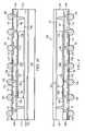
- FIGS. 3 a - 3 killustrate, in relation to FIGS. 1 and a- 2 c , a process of mounting semiconductor die to a heat spreader on a temporary carrier and forming polymer layers and conductive layers over the die.
- semiconductor wafer 120contains a plurality of semiconductor die 122 separated by saw street 124 .
- Each semiconductor die 122contains analog or digital circuits implemented as active devices, passive devices, conductive layers, and dielectric layers formed within the die and electrically interconnected according to the electrical design and function of the die.
- the circuitmay include one or more transistors, diodes, and other circuit elements formed within the active surface of the die to implement analog circuits or digital circuits, such as digital signal processor (DSP), ASIC, memory, or other signal processing circuit.
- DSPdigital signal processor
- Semiconductor die 122may also contain IPD, such as inductors, capacitors, and resistors, for RF signal processing.
- IPDsuch as inductors, capacitors, and resistors
- a wafer-form substrate or carrier 130contains temporary or sacrificial base material such as silicon, polymer, polymer composite, metal, ceramic, glass, glass epoxy, beryllium oxide, or other suitable low-cost, rigid material or bulk semiconductor material for structural support.
- carrier 130is 20.3 centimeters (cm) in diameter.
- Adhesive tape 132is formed on carrier 130 , as shown in FIG. 3 c .
- An array of conductive heat spreaders 134is disposed on adhesive tape 132 , as shown in FIGS. 3 b and 3 d. Heat spreaders 134 can be Al, Cu, or another material with high thermal conductivity to provide heat dissipation.
- Semiconductor die 122are singulated from wafer 120 and picked and placed onto heat spreader 134 with back surface 135 of the die oriented toward heat spreader 134 and contact pads 138 and active surface 140 of the die oriented away from carrier 130 .
- An optional die attach adhesive or thermal interface layer (TIM) 136holds semiconductor die 122 in place during the re-array of the die onto heat spreaders 134 .
- an insulating layer 142is formed over semiconductor die 122 and heat spreader 134 .
- the insulating layer 142can be one or more layers of polyimide, BCB, PBO, polynorbornene, epoxy resin with filler, epoxy acrylate with filler, or other polymer material.
- the insulating layer 142is formed using printing, spin coating, or spray coating.
- the insulating layer 142eliminates the need for a molding process.
- the insulating layer 142is planarized to expose contact pads 138 .
- a plurality of vias 144are drilled or etched into insulating layer 142 . Vias 144 extend down to heat spreader 134 .
- an electrically conductive layer 146is formed over insulating layer 142 and into vias 144 using a patterning and metal deposition process such as PVD, CVD, sputtering, electrolytic plating, or electroless plating process.
- Conductive layer 146can be one or more layers of Al, Cu, Sn, Ni, Au, Ag, or other suitable electrically conductive material.
- One portion of conductive layer 146is electrically connected to contact pads 138 of semiconductor die 122 ; another portion of conductive layer 146 is thermally connected to heat spreader 134 .
- Other portions of conductive layer 146can be electrically common or electrically isolated depending on the design and function of the semiconductor device.
- an insulating layer 148is formed over insulating layer 142 and conductive layer 146 .
- the insulating layer 148can be one or more layers of polyimide, BCB, PBO, polynorbornene, epoxy resin with filler, epoxy acrylate with filler, or other polymer material.
- the insulating layer 148is formed using printing, spin coating, or spray coating.
- a portion of insulating layer 148is removed by drilling or etch development process to form vias 150 down to conductive layer 146 .
- an electrically conductive layer 152is formed over insulating layer 148 and into vias 150 using a patterning and metal deposition process such as PVD, CVD, sputtering, electrolytic plating, or electroless plating process.
- Conductive layer 152can be one or more layers of Al, Cu, Sn, Ni, Au, Ag, or other suitable electrically conductive material.
- One portion of conductive layer 152is electrically connected to conductive layer 146 .
- Other portions of conductive layer 152can be electrically common or electrically isolated depending on the design and function of the semiconductor device.
- Conductive layers 146 and 152use redistribution to transfer signals from a peripheral layout to an area array.
- a solder masking layer 154is formed over conductive layer 152 and insulating layer 148 with openings to expose conductive layer 152 for next level interconnect.
- An electrically conductive bump materialis deposited over conductive layer 152 using an evaporation, electrolytic plating, electroless plating, ball drop, or screen printing process.
- the bump materialcan be Al, Sn, Ni, Au, Ag, Pb, Bi, Cu, solder, and combinations thereof, with an optional flux solution.
- the bump materialcan be eutectic Sn/Pb, high-lead solder, or lead-free solder.
- the bump materialis bonded to conductive layer 152 using a suitable attachment or bonding process. In one embodiment, the bump material is reflowed by heating the material above its melting point to form spherical balls or bumps 156 .
- bumps 156are reflowed a second time to improve electrical contact to conductive layer 152 .
- the bumpscan also be compression bonded to conductive layer 152 .
- Bumps 156represent one type of interconnect structure that can be formed over conductive layer 152 .
- the interconnect structurecan also use bond wires, stud bump, micro bump, or other electrical interconnect.
- Carrier 130 and adhesive tape 132are removed by mechanical peel-off, CMP, mechanical grinding, thermal bake, laser scanning, or wet stripping.
- Semiconductor die 122are singulated into individual units using a saw blade or laser cutting tool.
- FIG. 4shows WLCSP 160 with back surface 135 of semiconductor die 122 directly mounted to heat spreader 134 .
- Heat spreader 134dissipates heat generated by semiconductor die 122 .
- Heat spreader 134also blocks or absorbs electromagnetic interference (EMI), radio frequency interference (RFI), and other inter-device interference.
- Heat spreader 134is grounded through conductive layers 146 and 152 to bumps 156 .
- Polymer layers 142 and 148as formed around and over semiconductor die 122 , eliminate the need for a molding process.
- Conductive layers 146 and 152provide a short signal path from contact pads 138 to bumps 156 for a higher operating speed and good electrical performance for semiconductor die 122 .
Landscapes
- Engineering & Computer Science (AREA)
- Microelectronics & Electronic Packaging (AREA)
- Computer Hardware Design (AREA)
- Power Engineering (AREA)
- Physics & Mathematics (AREA)
- General Physics & Mathematics (AREA)
- Condensed Matter Physics & Semiconductors (AREA)
- Manufacturing & Machinery (AREA)
- Chemical & Material Sciences (AREA)
- Materials Engineering (AREA)
- Health & Medical Sciences (AREA)
- Electromagnetism (AREA)
- Toxicology (AREA)
- Geometry (AREA)
- Structures Or Materials For Encapsulating Or Coating Semiconductor Devices Or Solid State Devices (AREA)
Abstract
Description
- The present invention relates in general to semiconductor devices and, more particularly, to a semiconductor device and method of mounting a semiconductor die to a heat spreader on a temporary carrier and forming polymer layers and conductive layers over the die.
- Semiconductor devices are commonly found in modern electronic products. Semiconductor devices vary in the number and density of electrical components. Discrete semiconductor devices generally contain one type of electrical component, e.g., light emitting diode (LED), small signal transistor, resistor, capacitor, inductor, and power metal oxide semiconductor field effect transistor (MOSFET). Integrated semiconductor devices typically contain hundreds to millions of electrical components. Examples of integrated semiconductor devices include microcontrollers, microprocessors, charged-coupled devices (CCDs), solar cells, and digital micro-mirror devices (DMDs).
- Semiconductor devices perform a wide range of functions such as high-speed calculations, transmitting and receiving electromagnetic signals, controlling electronic devices, transforming sunlight to electricity, and creating visual projections for television displays. Semiconductor devices are found in the fields of entertainment, communications, power conversion, networks, computers, and consumer products. Semiconductor devices are also found in military applications, aviation, automotive, industrial controllers, and office equipment.
- Semiconductor devices exploit the electrical properties of semiconductor materials. The atomic structure of semiconductor material allows its electrical conductivity to be manipulated by the application of an electric field or base current or through the process of doping. Doping introduces impurities into the semiconductor material to manipulate and control the conductivity of the semiconductor device.
- A semiconductor device contains active and passive electrical structures. Active structures, including bipolar and field effect transistors, control the flow of electrical current. By varying levels of doping and application of an electric field or base current, the transistor either promotes or restricts the flow of electrical current. Passive structures, including resistors, capacitors, and inductors, create a relationship between voltage and current necessary to perform a variety of electrical functions. The passive and active structures are electrically connected to form circuits, which enable the semiconductor device to perform high-speed calculations and other useful functions.
- Semiconductor devices are generally manufactured using two complex manufacturing processes, i.e., front-end manufacturing, and back-end manufacturing, each involving potentially hundreds of steps. Front-end manufacturing involves the formation of a plurality of die on the surface of a semiconductor wafer. Each die is typically identical and contains circuits formed by electrically connecting active and passive components. Back-end manufacturing involves singulating individual die from the finished wafer and packaging the die to provide structural support and environmental isolation.
- One goal of semiconductor manufacturing is to produce smaller semiconductor devices. Smaller devices typically consume less power, have higher performance, and can be produced more efficiently. In addition, smaller semiconductor devices have a smaller footprint, which is desirable for smaller end products. A smaller die size may be achieved by improvements in the front-end process resulting in die with smaller, higher density active and passive components. Back-end processes may result in semiconductor device packages with a smaller footprint by improvements in electrical interconnection and packaging materials.
- In fan-out wafer level chip scale packages (FO-WLCSP), semiconductor die are stacked and vertically interconnected within the package. In high frequency applications, the semiconductor die emit or are susceptible to radiation, electromagnetic interference (EMI), radio frequency interference (RFI), harmonic effects, and other inter-device interference, which reduces the electrical performance of the device. In addition, the high frequency semiconductor die generate considerable thermal energy which must be adequately dissipated.
- A need exists to dissipate thermal energy and shield against inter-device interference in a FO-WLCSP. Accordingly, in one embodiment, the present invention is a method of making a semiconductor device comprising the steps of providing a temporary carrier, forming a heat spreader over the temporary carrier, mounting a semiconductor die to the heat spreader, forming a first insulating layer over the semiconductor die and heat spreader, and forming a first conductive layer over the first insulating layer. The first conductive layer is connected to the heat spreader and contact pads on the semiconductor die. The method further includes the steps of forming a second insulating layer over the first conductive layer, and forming a second conductive layer over the second insulating layer. The second conductive layer is electrically connected to the first conductive layer. The temporary carrier is removed.
- In another embodiment, the present invention is a method of making a semiconductor device comprising the steps of providing a temporary carrier, forming a heat spreader over the temporary carrier, mounting a semiconductor die to the heat spreader, forming a first insulating layer over the semiconductor die and heat spreader, and forming a first conductive layer over the first insulating layer. The first conductive layer is connected to the heat spreader and contact pads on the semiconductor die. The temporary carrier is removed.
- In another embodiment, the present invention is a method of making a semiconductor device comprising the steps of providing a heat spreader, mounting a backside of a semiconductor die to the heat spreader, forming a first insulating layer over an active side of the semiconductor die and heat spreader, and forming a first conductive layer over the first insulating layer. The first conductive layer is connected to the heat spreader and contact pads on the semiconductor die.
- In another embodiment, the present invention is a semiconductor device comprising a heat spreader and semiconductor die having a backside mounted to the heat spreader. A first insulating layer is formed over an active side of the semiconductor die and heat spreader. A first conductive layer is formed over the first insulating layer. The first conductive layer is connected to the heat spreader and contact pads on the semiconductor die.
FIG. 1 illustrates a PCB with different types of packages mounted to its surface;FIGS. 2 a-2cillustrate further detail of the representative semiconductor packages mounted to the PCB;FIGS. 3 a-3killustrate a process of mounting semiconductor die to a heat spreader on a temporary carrier and forming polymer layers and conductive layers over the die; andFIG. 4 illustrates the semiconductor die mounted to the heat spreader with polymer layers and conductive layers formed over and around the die.- The present invention is described in one or more embodiments in the following description with reference to the figures, in which like numerals represent the same or similar elements. While the invention is described in terms of the best mode for achieving the invention's objectives, it will be appreciated by those skilled in the art that it is intended to cover alternatives, modifications, and equivalents as may be included within the spirit and scope of the invention as defined by the appended claims and their equivalents as supported by the following disclosure and drawings.
- Semiconductor devices are generally manufactured using two complex manufacturing processes: front-end manufacturing and back-end manufacturing. Front-end manufacturing involves the formation of a plurality of die on the surface of a semiconductor wafer. Each die on the wafer contains active and passive electrical components, which are electrically connected to form functional electrical circuits. Active electrical components, such as transistors and diodes, have the ability to control the flow of electrical current. Passive electrical components, such as capacitors, inductors, resistors, and transformers, create a relationship between voltage and current necessary to perform electrical circuit functions.
- Passive and active components are formed over the surface of the semiconductor wafer by a series of process steps including doping, deposition, photolithography, etching, and planarization. Doping introduces impurities into the semiconductor material by techniques such as ion implantation or thermal diffusion. The doping process modifies the electrical conductivity of semiconductor material in active devices, transforming the semiconductor material into an insulator, conductor, or dynamically changing the semiconductor material conductivity in response to an electric field or base current. Transistors contain regions of varying types and degrees of doping arranged as necessary to enable the transistor to promote or restrict the flow of electrical current upon the application of the electric field or base current.
- Active and passive components are formed by layers of materials with different electrical properties. The layers can be formed by a variety of deposition techniques determined in part by the type of material being deposited. For example, thin film deposition may involve chemical vapor deposition (CVD), physical vapor deposition (PVD), electrolytic plating, and electroless plating processes. Each layer is generally patterned to form portions of active components, passive components, or electrical connections between components.
- The layers can be patterned using photolithography, which involves the deposition of light sensitive material, e.g., photoresist, over the layer to be patterned. A pattern is transferred from a photomask to the photoresist using light. The portion of the photoresist pattern subjected to light is removed using a solvent, exposing portions of the underlying layer to be patterned. The remainder of the photoresist is removed, leaving behind a patterned layer. Alternatively, some types of materials are patterned by directly depositing the material into the areas or voids formed by a previous deposition/etch process using techniques such as electroless and electrolytic plating.
- Depositing a thin film of material over an existing pattern can exaggerate the underlying pattern and create a non-uniformly flat surface. A uniformly flat surface is required to produce smaller and more densely packed active and passive components. Planarization can be used to remove material from the surface of the wafer and produce a uniformly flat surface. Planarization involves polishing the surface of the wafer with a polishing pad. An abrasive material and corrosive chemical are added to the surface of the wafer during polishing. The combined mechanical action of the abrasive and corrosive action of the chemical removes any irregular topography, resulting in a uniformly flat surface.
- Back-end manufacturing refers to cutting or singulating the finished wafer into the individual die and then packaging the die for structural support and environmental isolation. To singulate the die, the wafer is scored and broken along non-functional regions of the wafer called saw streets or scribes. The wafer is singulated using a laser cutting tool or saw blade. After singulation, the individual die are mounted to a package substrate that includes pins or contact pads for interconnection with other system components. Contact pads formed over the semiconductor die are then connected to contact pads within the package. The electrical connections can be made with solder bumps, stud bumps, conductive paste, or wirebonds. An encapsulant or other molding material is deposited over the package to provide physical support and electrical isolation. The finished package is then inserted into an electrical system and the functionality of the semiconductor device is made available to the other system components.
FIG. 1 illustrateselectronic device 50 having a chip carrier substrate or printed circuit board (PCB)52 with a plurality of semiconductor packages mounted on its surface.Electronic device 50 may have one type of semiconductor package, or multiple types of semiconductor packages, depending on the application. The different types of semiconductor packages are shown inFIG. 1 for purposes of illustration.Electronic device 50 may be a stand-alone system that uses the semiconductor packages to perform one or more electrical functions. Alternatively,electronic device 50 may be a subcomponent of a larger system. For example,electronic device 50 may be a graphics card, network interface card, or other signal processing card that can be inserted into a computer. The semiconductor package can include microprocessors, memories, application specific integrated circuits (ASIC), logic circuits, analog circuits, RF circuits, discrete devices, or other semiconductor die or electrical components.- In
FIG. 1 ,PCB 52 provides a general substrate for structural support and electrical interconnect of the semiconductor packages mounted on the PCB. Conductive signal traces54 are formed over a surface or within layers ofPCB 52 using evaporation, electrolytic plating, electroless plating, screen printing, or other suitable metal deposition process. Signal traces54 provide for electrical communication between each of the semiconductor packages, mounted components, and other external system components.Traces 54 also provide power and ground connections to each of the semiconductor packages. - In some embodiments, a semiconductor device has two packaging levels. First level packaging is a technique for mechanically and electrically attaching the semiconductor die to an intermediate carrier. Second level packaging involves mechanically and electrically attaching the intermediate carrier to the PCB. In other embodiments, a semiconductor device may only have the first level packaging where the die is mechanically and electrically mounted directly to the PCB.
- For the purpose of illustration, several types of first level packaging, including
wire bond package 56 andflip chip 58, are shown onPCB 52. Additionally, several types of second level packaging, including ball grid array (BGA)60, bump chip carrier (BCC)62, dual in-line package (DIP)64, land grid array (LGA)66, multi-chip module (MCM)68, quad flat non-leaded package (QFN)70, and quadflat package 72, are shown mounted onPCB 52. Depending upon the system requirements, any combination of semiconductor packages, configured with any combination of first and second level packaging styles, as well as other electronic components, can be connected toPCB 52. In some embodiments,electronic device 50 includes a single attached semiconductor package, while other embodiments call for multiple interconnected packages. By combining one or more semiconductor packages over a single substrate, manufacturers can incorporate pre-made components into electronic devices and systems. Because the semiconductor packages include sophisticated functionality, electronic devices can be manufactured using cheaper components and a streamlined manufacturing process. The resulting devices are less likely to fail and less expensive to manufacture resulting in a lower cost for consumers. FIGS. 2 a-2cshow exemplary semiconductor packages.FIG. 2 aillustrates further detail ofDIP 64 mounted onPCB 52. Semiconductor die74 includes an active region containing analog or digital circuits implemented as active devices, passive devices, conductive layers, and dielectric layers formed within the die and are electrically interconnected according to the electrical design of the die. For example, the circuit may include one or more transistors, diodes, inductors, capacitors, resistors, and other circuit elements formed within the active region of semiconductor die74. Contactpads 76 are one or more layers of conductive material, such as aluminum (Al), copper (Cu), tin (Sn), nickel (Ni), gold (Au), or silver (Ag), and are electrically connected to the circuit elements formed within semiconductor die74. During assembly ofDIP 64, semiconductor die74 is mounted to anintermediate carrier 78 using a gold-silicon eutectic layer or adhesive material such as thermal epoxy. The package body includes an insulative packaging material such as polymer or ceramic. Conductor leads80 andwire bonds 82 provide electrical interconnect between semiconductor die74 andPCB 52.Encapsulant 84 is deposited over the package for environmental protection by preventing moisture and particles from entering the package and contaminating die74 or wire bonds82.FIG. 2 billustrates further detail ofBCC 62 mounted onPCB 52. Semiconductor die88 is mounted overcarrier 90 using an underfill or epoxy-resin adhesive material 92.Wire bonds 94 provide first level packing interconnect betweencontact pads encapsulant 100 is deposited over semiconductor die88 andwire bonds 94 to provide physical support and electrical isolation for the device. Contactpads 102 are formed over a surface ofPCB 52 using a suitable metal deposition process such as electrolytic plating or electroless plating to prevent oxidation. Contactpads 102 are electrically connected to one or more conductive signal traces54 inPCB 52.Bumps 104 are formed betweencontact pads 98 ofBCC 62 andcontact pads 102 ofPCB 52.- In
FIG. 2 c,semiconductor die58 is mounted face down tointermediate carrier 106 with a flip chip style first level packaging.Active region 108 of semiconductor die58 contains analog or digital circuits implemented as active devices, passive devices, conductive layers, and dielectric layers formed according to the electrical design of the die. For example, the circuit may include one or more transistors, diodes, inductors, capacitors, resistors, and other circuit elements withinactive region 108. Semiconductor die58 is electrically and mechanically connected tocarrier 106 throughbumps 110. BGA 60 is electrically and mechanically connected toPCB 52 with a BGA style second levelpackaging using bumps 112. Semiconductor die58 is electrically connected to conductive signal traces54 inPCB 52 throughbumps 110,signal lines 114, and bumps112. A molding compound orencapsulant 116 is deposited over semiconductor die58 andcarrier 106 to provide physical support and electrical isolation for the device. The flip chip semiconductor device provides a short electrical conduction path from the active devices on semiconductor die58 to conduction tracks onPCB 52 in order to reduce signal propagation distance, lower capacitance, and improve overall circuit performance. In another embodiment, the semiconductor die58 can be mechanically and electrically connected directly toPCB 52 using flip chip style first level packaging withoutintermediate carrier 106.FIGS. 3 a-3killustrate, in relation toFIGS. 1 and a-2c, a process of mounting semiconductor die to a heat spreader on a temporary carrier and forming polymer layers and conductive layers over the die. InFIG. 3 a,semiconductor wafer 120 contains a plurality of semiconductor die122 separated by sawstreet 124. Each semiconductor die122 contains analog or digital circuits implemented as active devices, passive devices, conductive layers, and dielectric layers formed within the die and electrically interconnected according to the electrical design and function of the die. For example, the circuit may include one or more transistors, diodes, and other circuit elements formed within the active surface of the die to implement analog circuits or digital circuits, such as digital signal processor (DSP), ASIC, memory, or other signal processing circuit. Semiconductor die122 may also contain IPD, such as inductors, capacitors, and resistors, for RF signal processing. A typical RF system requires multiple IPDs in one or more semiconductor packages to perform the necessary electrical functions.- In
FIG. 3 b,a wafer-form substrate orcarrier 130 contains temporary or sacrificial base material such as silicon, polymer, polymer composite, metal, ceramic, glass, glass epoxy, beryllium oxide, or other suitable low-cost, rigid material or bulk semiconductor material for structural support. In one embodiment,carrier 130 is 20.3 centimeters (cm) in diameter.Adhesive tape 132 is formed oncarrier 130, as shown inFIG. 3 c. An array ofconductive heat spreaders 134 is disposed onadhesive tape 132, as shown inFIGS. 3 band3d.Heatspreaders 134 can be Al, Cu, or another material with high thermal conductivity to provide heat dissipation. Semiconductor die122 are singulated fromwafer 120 and picked and placed ontoheat spreader 134 withback surface 135 of the die oriented towardheat spreader 134 andcontact pads 138 andactive surface 140 of the die oriented away fromcarrier 130. An optional die attach adhesive or thermal interface layer (TIM)136 holds semiconductor die122 in place during the re-array of the die ontoheat spreaders 134. - In
FIG. 3 e,an insulatinglayer 142 is formed over semiconductor die122 andheat spreader 134. The insulatinglayer 142 can be one or more layers of polyimide, BCB, PBO, polynorbornene, epoxy resin with filler, epoxy acrylate with filler, or other polymer material. The insulatinglayer 142 is formed using printing, spin coating, or spray coating. The insulatinglayer 142 eliminates the need for a molding process. The insulatinglayer 142 is planarized to exposecontact pads 138. InFIG. 3 f,a plurality ofvias 144 are drilled or etched into insulatinglayer 142.Vias 144 extend down toheat spreader 134. - In
FIG. 3 g,an electricallyconductive layer 146 is formed overinsulating layer 142 and intovias 144 using a patterning and metal deposition process such as PVD, CVD, sputtering, electrolytic plating, or electroless plating process.Conductive layer 146 can be one or more layers of Al, Cu, Sn, Ni, Au, Ag, or other suitable electrically conductive material. One portion ofconductive layer 146 is electrically connected to contactpads 138 of semiconductor die122; another portion ofconductive layer 146 is thermally connected to heatspreader 134. Other portions ofconductive layer 146 can be electrically common or electrically isolated depending on the design and function of the semiconductor device. - In
FIG. 3 h,an insulatinglayer 148 is formed overinsulating layer 142 andconductive layer 146. The insulatinglayer 148 can be one or more layers of polyimide, BCB, PBO, polynorbornene, epoxy resin with filler, epoxy acrylate with filler, or other polymer material. The insulatinglayer 148 is formed using printing, spin coating, or spray coating. InFIG. 3 i,a portion of insulatinglayer 148 is removed by drilling or etch development process to form vias150 down toconductive layer 146. - In
FIG. 3 j,an electricallyconductive layer 152 is formed overinsulating layer 148 and intovias 150 using a patterning and metal deposition process such as PVD, CVD, sputtering, electrolytic plating, or electroless plating process.Conductive layer 152 can be one or more layers of Al, Cu, Sn, Ni, Au, Ag, or other suitable electrically conductive material. One portion ofconductive layer 152 is electrically connected toconductive layer 146. Other portions ofconductive layer 152 can be electrically common or electrically isolated depending on the design and function of the semiconductor device.Conductive layers - In
FIG. 3 k,asolder masking layer 154 is formed overconductive layer 152 and insulatinglayer 148 with openings to exposeconductive layer 152 for next level interconnect. - An electrically conductive bump material is deposited over
conductive layer 152 using an evaporation, electrolytic plating, electroless plating, ball drop, or screen printing process. The bump material can be Al, Sn, Ni, Au, Ag, Pb, Bi, Cu, solder, and combinations thereof, with an optional flux solution. For example, the bump material can be eutectic Sn/Pb, high-lead solder, or lead-free solder. The bump material is bonded toconductive layer 152 using a suitable attachment or bonding process. In one embodiment, the bump material is reflowed by heating the material above its melting point to form spherical balls or bumps156. In some applications, bumps156 are reflowed a second time to improve electrical contact toconductive layer 152. The bumps can also be compression bonded toconductive layer 152.Bumps 156 represent one type of interconnect structure that can be formed overconductive layer 152. The interconnect structure can also use bond wires, stud bump, micro bump, or other electrical interconnect. Carrier 130 andadhesive tape 132 are removed by mechanical peel-off, CMP, mechanical grinding, thermal bake, laser scanning, or wet stripping. Semiconductor die122 are singulated into individual units using a saw blade or laser cutting tool.FIG. 4 showsWLCSP 160 withback surface 135 of semiconductor die122 directly mounted toheat spreader 134.Heat spreader 134 dissipates heat generated by semiconductor die122.Heat spreader 134 also blocks or absorbs electromagnetic interference (EMI), radio frequency interference (RFI), and other inter-device interference.Heat spreader 134 is grounded throughconductive layers bumps 156. Polymer layers142 and148, as formed around and over semiconductor die122, eliminate the need for a molding process.Conductive layers contact pads 138 tobumps 156 for a higher operating speed and good electrical performance for semiconductor die122.- While one or more embodiments of the present invention have been illustrated in detail, the skilled artisan will appreciate that modifications and adaptations to those embodiments may be made without departing from the scope of the present invention as set forth in the following claims.
Claims (25)
Priority Applications (3)
| Application Number | Priority Date | Filing Date | Title |
|---|---|---|---|
| US12/541,334US8003496B2 (en) | 2009-08-14 | 2009-08-14 | Semiconductor device and method of mounting semiconductor die to heat spreader on temporary carrier and forming polymer layer and conductive layer over the die |
| US13/190,339US9048209B2 (en) | 2009-08-14 | 2011-07-25 | Semiconductor device and method of mounting semiconductor die to heat spreader on temporary carrier and forming polymer layer and conductive layer over the die |
| US14/697,950US9379064B2 (en) | 2009-08-14 | 2015-04-28 | Semiconductor device and method of mounting semiconductor die to heat spreader on temporary carrier and forming polymer layer and conductive layer over the die |
Applications Claiming Priority (1)
| Application Number | Priority Date | Filing Date | Title |
|---|---|---|---|
| US12/541,334US8003496B2 (en) | 2009-08-14 | 2009-08-14 | Semiconductor device and method of mounting semiconductor die to heat spreader on temporary carrier and forming polymer layer and conductive layer over the die |
Related Child Applications (1)
| Application Number | Title | Priority Date | Filing Date |
|---|---|---|---|
| US13/190,339ContinuationUS9048209B2 (en) | 2009-08-14 | 2011-07-25 | Semiconductor device and method of mounting semiconductor die to heat spreader on temporary carrier and forming polymer layer and conductive layer over the die |
Publications (2)
| Publication Number | Publication Date |
|---|---|
| US20110037165A1true US20110037165A1 (en) | 2011-02-17 |
| US8003496B2 US8003496B2 (en) | 2011-08-23 |
Family
ID=43588110
Family Applications (3)
| Application Number | Title | Priority Date | Filing Date |
|---|---|---|---|
| US12/541,334Active2029-08-27US8003496B2 (en) | 2009-08-14 | 2009-08-14 | Semiconductor device and method of mounting semiconductor die to heat spreader on temporary carrier and forming polymer layer and conductive layer over the die |
| US13/190,339Active2029-11-29US9048209B2 (en) | 2009-08-14 | 2011-07-25 | Semiconductor device and method of mounting semiconductor die to heat spreader on temporary carrier and forming polymer layer and conductive layer over the die |
| US14/697,950ActiveUS9379064B2 (en) | 2009-08-14 | 2015-04-28 | Semiconductor device and method of mounting semiconductor die to heat spreader on temporary carrier and forming polymer layer and conductive layer over the die |
Family Applications After (2)
| Application Number | Title | Priority Date | Filing Date |
|---|---|---|---|
| US13/190,339Active2029-11-29US9048209B2 (en) | 2009-08-14 | 2011-07-25 | Semiconductor device and method of mounting semiconductor die to heat spreader on temporary carrier and forming polymer layer and conductive layer over the die |
| US14/697,950ActiveUS9379064B2 (en) | 2009-08-14 | 2015-04-28 | Semiconductor device and method of mounting semiconductor die to heat spreader on temporary carrier and forming polymer layer and conductive layer over the die |
Country Status (1)
| Country | Link |
|---|---|
| US (3) | US8003496B2 (en) |
Cited By (12)
| Publication number | Priority date | Publication date | Assignee | Title |
|---|---|---|---|---|
| EP2560201A3 (en)* | 2011-08-19 | 2014-07-02 | Unimicron Technology Corp. | Semiconductor packaging structure and method of fabricating the same |
| US20140226283A1 (en)* | 2013-02-13 | 2014-08-14 | Gerald Ho Kim | Isolation Of Thermal Ground For Multiple Heat-Generating Devices On A Substrate |
| US20160005705A1 (en)* | 2014-07-01 | 2016-01-07 | Texas Instruments Incorporated | Structure and Method of Batch-Packaging Low Pin Count Embedded Semiconductor Chips |
| WO2016209172A1 (en)* | 2015-06-26 | 2016-12-29 | Pep Innovation Pte Ltd | Semiconductor packaging method, semiconductor package and stacked semiconductor packages |
| US9553036B1 (en)* | 2015-07-09 | 2017-01-24 | Powertech Technology Inc. | Semiconductor package and manufacturing method thereof |
| CN107720689A (en)* | 2011-06-30 | 2018-02-23 | 村田电子有限公司 | The manufacture method and system in package device of system in package device |
| CN108933127A (en)* | 2017-05-22 | 2018-12-04 | 海华科技股份有限公司 | Portable electronic device and image acquisition module and bearing assembly thereof |
| US10916488B2 (en)* | 2018-06-29 | 2021-02-09 | Taiwan Semiconductor Manufacturing Company, Ltd. | Semiconductor package having thermal conductive pattern surrounding the semiconductor die |
| CN113629018A (en)* | 2020-05-06 | 2021-11-09 | 讯芯电子科技(中山)有限公司 | Semiconductor package device and semiconductor package device manufacturing method |
| CN113785393A (en)* | 2021-07-28 | 2021-12-10 | 广东省科学院半导体研究所 | Fan-out package and manufacturing method thereof |
| US20220084974A1 (en)* | 2019-06-10 | 2022-03-17 | Rising Technologies Co., Ltd. | Electronic circuit device |
| CN115223902A (en)* | 2022-09-21 | 2022-10-21 | 西北电子装备技术研究所(中国电子科技集团公司第二研究所) | Pressurization of high accuracy eutectic chip mounter is got and is put structure |
Families Citing this family (29)
| Publication number | Priority date | Publication date | Assignee | Title |
|---|---|---|---|---|
| US7838985B2 (en)* | 2007-07-12 | 2010-11-23 | Vishay General Semiconductor Llc | Semiconductor assembly that includes a power semiconductor die located on a cell defined by first and second patterned polymer layers |
| US8409963B2 (en)* | 2009-04-28 | 2013-04-02 | CDA Procesing Limited Liability Company | Methods of embedding thin-film capacitors into semiconductor packages using temporary carrier layers |
| US8003496B2 (en) | 2009-08-14 | 2011-08-23 | Stats Chippac, Ltd. | Semiconductor device and method of mounting semiconductor die to heat spreader on temporary carrier and forming polymer layer and conductive layer over the die |
| US8884422B2 (en) | 2009-12-31 | 2014-11-11 | Stmicroelectronics Pte Ltd. | Flip-chip fan-out wafer level package for package-on-package applications, and method of manufacture |
| US8502394B2 (en)* | 2009-12-31 | 2013-08-06 | Stmicroelectronics Pte Ltd. | Multi-stacked semiconductor dice scale package structure and method of manufacturing same |
| US20110156240A1 (en)* | 2009-12-31 | 2011-06-30 | Stmicroelectronics Asia Pacific Pte. Ltd. | Reliable large die fan-out wafer level package and method of manufacture |
| US8466997B2 (en)* | 2009-12-31 | 2013-06-18 | Stmicroelectronics Pte Ltd. | Fan-out wafer level package for an optical sensor and method of manufacture thereof |
| US8436255B2 (en)* | 2009-12-31 | 2013-05-07 | Stmicroelectronics Pte Ltd. | Fan-out wafer level package with polymeric layer for high reliability |
| US8410598B2 (en)* | 2010-12-30 | 2013-04-02 | STMicroeletronics Pte. Ltd. | Semiconductor package and method of manufacturing the same |
| US9013037B2 (en) | 2011-09-14 | 2015-04-21 | Stmicroelectronics Pte Ltd. | Semiconductor package with improved pillar bump process and structure |
| US8916481B2 (en) | 2011-11-02 | 2014-12-23 | Stmicroelectronics Pte Ltd. | Embedded wafer level package for 3D and package-on-package applications, and method of manufacture |
| US8779601B2 (en) | 2011-11-02 | 2014-07-15 | Stmicroelectronics Pte Ltd | Embedded wafer level package for 3D and package-on-package applications, and method of manufacture |
| KR101458755B1 (en)* | 2013-06-13 | 2014-11-07 | 에스티에스반도체통신 주식회사 | wafer level package with the heat spreader and the manufacturing method thereof |
| KR20150053579A (en)* | 2013-11-08 | 2015-05-18 | 삼성전기주식회사 | Electric component module and manufacturing method threrof |
| US9706668B2 (en)* | 2014-10-24 | 2017-07-11 | Samsung Electro-Mechanics Co., Ltd. | Printed circuit board, electronic module and method of manufacturing the same |
| US10008472B2 (en)* | 2015-06-29 | 2018-06-26 | Stmicroelectronics, Inc. | Method for making semiconductor device with sidewall recess and related devices |
| KR102444235B1 (en)* | 2015-08-13 | 2022-09-16 | 삼성전자주식회사 | MRAM device and semiconductor package having magnetic shielding layer, and method for manufacturing the same |
| CN109075151B (en) | 2016-04-26 | 2023-06-27 | 亚德诺半导体国际无限责任公司 | Lead frame for mechanical mating, and electrical and thermal conduction of component package circuits |
| US10777478B2 (en)* | 2016-07-15 | 2020-09-15 | Advanced Semiconductor Engineering, Inc. | Semiconductor package device for power device |
| US10170341B1 (en)* | 2017-06-30 | 2019-01-01 | Taiwan Semiconductor Manufacturing Company, Ltd. | Release film as isolation film in package |
| DE102017126028B4 (en) | 2017-06-30 | 2020-12-10 | Taiwan Semiconductor Manufacturing Co., Ltd. | Housing and manufacturing method using a release film as an insulating film |
| US10497635B2 (en) | 2018-03-27 | 2019-12-03 | Linear Technology Holding Llc | Stacked circuit package with molded base having laser drilled openings for upper package |
| US10510595B2 (en) | 2018-04-30 | 2019-12-17 | Taiwan Semiconductor Manufacturing Company, Ltd. | Integrated fan-out packages and methods of forming the same |
| US11410977B2 (en) | 2018-11-13 | 2022-08-09 | Analog Devices International Unlimited Company | Electronic module for high power applications |
| US10985109B2 (en)* | 2018-12-27 | 2021-04-20 | STATS ChipPAC Pte. Ltd. | Shielded semiconductor packages with open terminals and methods of making via two-step process |
| US11721657B2 (en) | 2019-06-14 | 2023-08-08 | Stmicroelectronics Pte Ltd | Wafer level chip scale package having varying thicknesses |
| US11844178B2 (en) | 2020-06-02 | 2023-12-12 | Analog Devices International Unlimited Company | Electronic component |
| US12002729B2 (en)* | 2021-07-30 | 2024-06-04 | Advanced Semiconductor Engineering, Inc. | Electronic package and method of manufacturing the same |
| FR3140985A1 (en)* | 2022-10-14 | 2024-04-19 | Commissariat A L'energie Atomique Et Aux Energies Alternatives | SIP TYPE ELECTRONIC DEVICE AND METHOD FOR PRODUCING SUCH A DEVICE |
Citations (14)
| Publication number | Priority date | Publication date | Assignee | Title |
|---|---|---|---|---|
| US5250843A (en)* | 1991-03-27 | 1993-10-05 | Integrated System Assemblies Corp. | Multichip integrated circuit modules |
| US5353498A (en)* | 1993-02-08 | 1994-10-11 | General Electric Company | Method for fabricating an integrated circuit module |
| US5841193A (en)* | 1996-05-20 | 1998-11-24 | Epic Technologies, Inc. | Single chip modules, repairable multichip modules, and methods of fabrication thereof |
| US20020070443A1 (en)* | 2000-12-08 | 2002-06-13 | Xiao-Chun Mu | Microelectronic package having an integrated heat sink and build-up layers |
| US6709897B2 (en)* | 2002-01-15 | 2004-03-23 | Unimicron Technology Corp. | Method of forming IC package having upward-facing chip cavity |
| US6841413B2 (en)* | 2002-01-07 | 2005-01-11 | Intel Corporation | Thinned die integrated circuit package |
| US20060237827A1 (en)* | 2005-04-21 | 2006-10-26 | Industrial Technology Research Institute | Thermal enhanced low profile package structure and method for fabricating the same |
| US20080105967A1 (en)* | 2003-12-03 | 2008-05-08 | Advanced Chip Engineering Technology Inc. | Fan out type wafer level package structure and method of the same |
| US7619901B2 (en)* | 2007-06-25 | 2009-11-17 | Epic Technologies, Inc. | Integrated structures and fabrication methods thereof implementing a cell phone or other electronic system |
| US7683268B2 (en)* | 2004-06-08 | 2010-03-23 | Sanyo Electric Co., Ltd. | Semiconductor module with high process accuracy, manufacturing method thereof, and semiconductor device therewith |
| US20100078783A1 (en)* | 2008-09-30 | 2010-04-01 | Infineon Technologies Ag | Device including two mounting surfaces |
| US20100090322A1 (en)* | 2008-10-15 | 2010-04-15 | Harry Hedler | Packaging Systems and Methods |
| US20100148325A1 (en)* | 2008-12-12 | 2010-06-17 | Gruenhagen Michael D | Semiconductor Dice with Backside Trenches Filled With Elastic Material For Improved Attachment, Packages Using the Same, and Methods of Making the Same |
| US20110018114A1 (en)* | 2009-07-22 | 2011-01-27 | Stats Chippac, Ltd. | Semiconductor Device and Method of Embedding Thermally Conductive Layer in Interconnect Structure for Heat Dissipation |
Family Cites Families (22)
| Publication number | Priority date | Publication date | Assignee | Title |
|---|---|---|---|---|
| US6326678B1 (en)* | 1993-09-03 | 2001-12-04 | Asat, Limited | Molded plastic package with heat sink and enhanced electrical performance |
| US6246111B1 (en)* | 2000-01-25 | 2001-06-12 | Siliconware Precision Industries Co., Ltd. | Universal lead frame type of quad flat non-lead package of semiconductor |
| TW490820B (en)* | 2000-10-04 | 2002-06-11 | Advanced Semiconductor Eng | Heat dissipation enhanced ball grid array package |
| TW574750B (en)* | 2001-06-04 | 2004-02-01 | Siliconware Precision Industries Co Ltd | Semiconductor packaging member having heat dissipation plate |
| US6534859B1 (en)* | 2002-04-05 | 2003-03-18 | St. Assembly Test Services Ltd. | Semiconductor package having heat sink attached to pre-molded cavities and method for creating the package |
| TWI241700B (en)* | 2003-01-22 | 2005-10-11 | Siliconware Precision Industries Co Ltd | Packaging assembly with integrated circuits redistribution routing semiconductor die and method for fabrication |
| TWI233677B (en)* | 2003-10-28 | 2005-06-01 | Advanced Semiconductor Eng | Ball grid array package and method thereof |
| TWI229433B (en)* | 2004-07-02 | 2005-03-11 | Phoenix Prec Technology Corp | Direct connection multi-chip semiconductor element structure |
| TWI255536B (en)* | 2005-02-02 | 2006-05-21 | Siliconware Precision Industries Co Ltd | Chip-stacked semiconductor package and fabrication method thereof |
| US8610262B1 (en)* | 2005-02-18 | 2013-12-17 | Utac Hong Kong Limited | Ball grid array package with improved thermal characteristics |
| US7511359B2 (en)* | 2005-12-29 | 2009-03-31 | Intel Corporation | Dual die package with high-speed interconnect |
| US7576429B2 (en)* | 2005-12-30 | 2009-08-18 | Fairchild Semiconductor Corporation | Packaged semiconductor device with dual exposed surfaces and method of manufacturing |
| US7675157B2 (en)* | 2006-01-30 | 2010-03-09 | Marvell World Trade Ltd. | Thermal enhanced package |
| US8030138B1 (en)* | 2006-07-10 | 2011-10-04 | National Semiconductor Corporation | Methods and systems of packaging integrated circuits |
| US7645638B2 (en)* | 2006-08-04 | 2010-01-12 | Stats Chippac Ltd. | Stackable multi-chip package system with support structure |
| JP2008124430A (en)* | 2006-10-18 | 2008-05-29 | Hitachi Ltd | Power semiconductor module |
| US8174119B2 (en)* | 2006-11-10 | 2012-05-08 | Stats Chippac, Ltd. | Semiconductor package with embedded die |
| JP5496445B2 (en)* | 2007-06-08 | 2014-05-21 | ルネサスエレクトロニクス株式会社 | Manufacturing method of semiconductor device |
| US8637341B2 (en)* | 2008-03-12 | 2014-01-28 | Infineon Technologies Ag | Semiconductor module |
| US7759163B2 (en)* | 2008-04-18 | 2010-07-20 | Infineon Technologies Ag | Semiconductor module |
| US7858443B2 (en) | 2009-03-09 | 2010-12-28 | Utac Hong Kong Limited | Leadless integrated circuit package having standoff contacts and die attach pad |
| US8003496B2 (en)* | 2009-08-14 | 2011-08-23 | Stats Chippac, Ltd. | Semiconductor device and method of mounting semiconductor die to heat spreader on temporary carrier and forming polymer layer and conductive layer over the die |
- 2009
- 2009-08-14USUS12/541,334patent/US8003496B2/enactiveActive
- 2011
- 2011-07-25USUS13/190,339patent/US9048209B2/enactiveActive
- 2015
- 2015-04-28USUS14/697,950patent/US9379064B2/enactiveActive
Patent Citations (14)
| Publication number | Priority date | Publication date | Assignee | Title |
|---|---|---|---|---|
| US5250843A (en)* | 1991-03-27 | 1993-10-05 | Integrated System Assemblies Corp. | Multichip integrated circuit modules |
| US5353498A (en)* | 1993-02-08 | 1994-10-11 | General Electric Company | Method for fabricating an integrated circuit module |
| US5841193A (en)* | 1996-05-20 | 1998-11-24 | Epic Technologies, Inc. | Single chip modules, repairable multichip modules, and methods of fabrication thereof |
| US20020070443A1 (en)* | 2000-12-08 | 2002-06-13 | Xiao-Chun Mu | Microelectronic package having an integrated heat sink and build-up layers |
| US6841413B2 (en)* | 2002-01-07 | 2005-01-11 | Intel Corporation | Thinned die integrated circuit package |
| US6709897B2 (en)* | 2002-01-15 | 2004-03-23 | Unimicron Technology Corp. | Method of forming IC package having upward-facing chip cavity |
| US20080105967A1 (en)* | 2003-12-03 | 2008-05-08 | Advanced Chip Engineering Technology Inc. | Fan out type wafer level package structure and method of the same |
| US7683268B2 (en)* | 2004-06-08 | 2010-03-23 | Sanyo Electric Co., Ltd. | Semiconductor module with high process accuracy, manufacturing method thereof, and semiconductor device therewith |
| US20060237827A1 (en)* | 2005-04-21 | 2006-10-26 | Industrial Technology Research Institute | Thermal enhanced low profile package structure and method for fabricating the same |
| US7619901B2 (en)* | 2007-06-25 | 2009-11-17 | Epic Technologies, Inc. | Integrated structures and fabrication methods thereof implementing a cell phone or other electronic system |
| US20100078783A1 (en)* | 2008-09-30 | 2010-04-01 | Infineon Technologies Ag | Device including two mounting surfaces |
| US20100090322A1 (en)* | 2008-10-15 | 2010-04-15 | Harry Hedler | Packaging Systems and Methods |
| US20100148325A1 (en)* | 2008-12-12 | 2010-06-17 | Gruenhagen Michael D | Semiconductor Dice with Backside Trenches Filled With Elastic Material For Improved Attachment, Packages Using the Same, and Methods of Making the Same |
| US20110018114A1 (en)* | 2009-07-22 | 2011-01-27 | Stats Chippac, Ltd. | Semiconductor Device and Method of Embedding Thermally Conductive Layer in Interconnect Structure for Heat Dissipation |
Cited By (18)
| Publication number | Priority date | Publication date | Assignee | Title |
|---|---|---|---|---|
| CN107720689A (en)* | 2011-06-30 | 2018-02-23 | 村田电子有限公司 | The manufacture method and system in package device of system in package device |
| EP2560201A3 (en)* | 2011-08-19 | 2014-07-02 | Unimicron Technology Corp. | Semiconductor packaging structure and method of fabricating the same |
| US20140226283A1 (en)* | 2013-02-13 | 2014-08-14 | Gerald Ho Kim | Isolation Of Thermal Ground For Multiple Heat-Generating Devices On A Substrate |
| US9258878B2 (en)* | 2013-02-13 | 2016-02-09 | Gerald Ho Kim | Isolation of thermal ground for multiple heat-generating devices on a substrate |
| CN106663672A (en)* | 2014-07-01 | 2017-05-10 | 德州仪器公司 | Structure and method of batch-packaging low pin count embedded semiconductor chips |
| US20160005705A1 (en)* | 2014-07-01 | 2016-01-07 | Texas Instruments Incorporated | Structure and Method of Batch-Packaging Low Pin Count Embedded Semiconductor Chips |
| JP2017526168A (en)* | 2014-07-01 | 2017-09-07 | 日本テキサス・インスツルメンツ株式会社 | Structure and method of batch packaging low pin count embedded semiconductor chip |
| WO2016209172A1 (en)* | 2015-06-26 | 2016-12-29 | Pep Innovation Pte Ltd | Semiconductor packaging method, semiconductor package and stacked semiconductor packages |
| CN106449434A (en)* | 2015-06-26 | 2017-02-22 | Pep创新私人有限公司 | Semiconductor packaging method, semiconductor package and stacked semiconductor packages |
| US10854531B2 (en) | 2015-06-26 | 2020-12-01 | Pep Innovation Pte Ltd. | Semiconductor packaging method, semiconductor package and stacked semiconductor packages |
| US9553036B1 (en)* | 2015-07-09 | 2017-01-24 | Powertech Technology Inc. | Semiconductor package and manufacturing method thereof |
| CN108933127A (en)* | 2017-05-22 | 2018-12-04 | 海华科技股份有限公司 | Portable electronic device and image acquisition module and bearing assembly thereof |
| US10916488B2 (en)* | 2018-06-29 | 2021-02-09 | Taiwan Semiconductor Manufacturing Company, Ltd. | Semiconductor package having thermal conductive pattern surrounding the semiconductor die |
| US20220084974A1 (en)* | 2019-06-10 | 2022-03-17 | Rising Technologies Co., Ltd. | Electronic circuit device |
| US12074130B2 (en)* | 2019-06-10 | 2024-08-27 | Rising Technologies Co., Ltd. | Electronic circuit device |
| CN113629018A (en)* | 2020-05-06 | 2021-11-09 | 讯芯电子科技(中山)有限公司 | Semiconductor package device and semiconductor package device manufacturing method |
| CN113785393A (en)* | 2021-07-28 | 2021-12-10 | 广东省科学院半导体研究所 | Fan-out package and manufacturing method thereof |
| CN115223902A (en)* | 2022-09-21 | 2022-10-21 | 西北电子装备技术研究所(中国电子科技集团公司第二研究所) | Pressurization of high accuracy eutectic chip mounter is got and is put structure |
Also Published As
| Publication number | Publication date |
|---|---|
| US9379064B2 (en) | 2016-06-28 |
| US20110278705A1 (en) | 2011-11-17 |
| US20150228590A1 (en) | 2015-08-13 |
| US8003496B2 (en) | 2011-08-23 |
| US9048209B2 (en) | 2015-06-02 |
Similar Documents
| Publication | Publication Date | Title |
|---|---|---|
| US9379064B2 (en) | Semiconductor device and method of mounting semiconductor die to heat spreader on temporary carrier and forming polymer layer and conductive layer over the die | |
| US9508626B2 (en) | Semiconductor device and method of forming openings in thermally-conductive frame of FO-WLCSP to dissipate heat and reduce package height | |
| US9443829B2 (en) | Semiconductor device and method of dual-molding die formed on opposite sides of build-up interconnect structure | |
| US8530274B2 (en) | Semiconductor device and method of forming air gap adjacent to stress sensitive region of the die | |
| US8367480B2 (en) | Semiconductor device and method of forming dam material around periphery of die to reduce warpage | |
| US9324672B2 (en) | Semiconductor device and method of forming dual-active sided semiconductor die in fan-out wafer level chip scale package | |
| US9305897B2 (en) | Semiconductor package and method of mounting semiconductor die to opposite sides of TSV substrate | |
| US9048306B2 (en) | Semiconductor device and method of forming open cavity in TSV interposer to contain semiconductor die in WLCSMP | |
| US8367470B2 (en) | Semiconductor device and method of forming cavity in build-up interconnect structure for short signal path between die | |
| US8283209B2 (en) | Semiconductor device and method of forming PiP with inner known good die interconnected with conductive bumps | |
| SG183777A1 (en) | Semiconductor device and method of forming compliant stress relief buffer around large array wlcsp | |
| US8916452B2 (en) | Semiconductor device and method of forming WLCSP using wafer sections containing multiple die |
Legal Events
| Date | Code | Title | Description |
|---|---|---|---|
| AS | Assignment | Owner name:STATS CHIPPAC, LTD., SINGAPORE Free format text:ASSIGNMENT OF ASSIGNORS INTEREST;ASSIGNORS:OH, JIHOON;LEE, SINJAE;KIM, JINGWAN;REEL/FRAME:023101/0150 Effective date:20090814 | |
| STCF | Information on status: patent grant | Free format text:PATENTED CASE | |
| FPAY | Fee payment | Year of fee payment:4 | |
| AS | Assignment | Owner name:CITICORP INTERNATIONAL LIMITED, AS COMMON SECURITY AGENT, HONG KONG Free format text:SECURITY INTEREST;ASSIGNORS:STATS CHIPPAC, INC.;STATS CHIPPAC LTD.;REEL/FRAME:036288/0748 Effective date:20150806 Owner name:CITICORP INTERNATIONAL LIMITED, AS COMMON SECURITY Free format text:SECURITY INTEREST;ASSIGNORS:STATS CHIPPAC, INC.;STATS CHIPPAC LTD.;REEL/FRAME:036288/0748 Effective date:20150806 | |
| AS | Assignment | Owner name:STATS CHIPPAC PTE. LTE., SINGAPORE Free format text:CHANGE OF NAME;ASSIGNOR:STATS CHIPPAC LTD.;REEL/FRAME:038378/0301 Effective date:20160329 | |
| MAFP | Maintenance fee payment | Free format text:PAYMENT OF MAINTENANCE FEE, 8TH YEAR, LARGE ENTITY (ORIGINAL EVENT CODE: M1552); ENTITY STATUS OF PATENT OWNER: LARGE ENTITY Year of fee payment:8 | |
| AS | Assignment | Owner name:STATS CHIPPAC PTE. LTD. FORMERLY KNOWN AS STATS CH Free format text:RELEASE BY SECURED PARTY;ASSIGNOR:CITICORP INTERNATIONAL LIMITED, AS COMMON SECURITY AGENT;REEL/FRAME:051285/0318 Effective date:20190503 Owner name:STATS CHIPPAC, INC., CALIFORNIA Free format text:RELEASE BY SECURED PARTY;ASSIGNOR:CITICORP INTERNATIONAL LIMITED, AS COMMON SECURITY AGENT;REEL/FRAME:051285/0318 Effective date:20190503 Owner name:STATS CHIPPAC PTE. LTD. FORMERLY KNOWN AS STATS CHIPPAC LTD., SINGAPORE Free format text:RELEASE BY SECURED PARTY;ASSIGNOR:CITICORP INTERNATIONAL LIMITED, AS COMMON SECURITY AGENT;REEL/FRAME:051285/0318 Effective date:20190503 | |
| AS | Assignment | Owner name:JCET SEMICONDUCTOR (SHAOXING) CO., LTD., CHINA Free format text:ASSIGNMENT OF ASSIGNORS INTEREST;ASSIGNOR:STATS CHIPPAC PTE. LTD.;REEL/FRAME:051365/0680 Effective date:20191128 | |
| MAFP | Maintenance fee payment | Free format text:PAYMENT OF MAINTENANCE FEE, 12TH YEAR, LARGE ENTITY (ORIGINAL EVENT CODE: M1553); ENTITY STATUS OF PATENT OWNER: LARGE ENTITY Year of fee payment:12 | |
| AS | Assignment | Owner name:STATS CHIPPAC PTE. LTD., SINGAPORE Free format text:CORRECTIVE ASSIGNMENT TO CORRECT THE ASSIGNEE'S NAME PREVIOUSLY RECORDED AT REEL: 038378 FRAME: 0301. ASSIGNOR(S) HEREBY CONFIRMS THE CHANGE OF NAME;ASSIGNOR:STATS CHIPPAC LTD.;REEL/FRAME:064913/0352 Effective date:20160329 |