US20110019374A1 - Z-Directed Delay Line Components for Printed Circuit Boards - Google Patents
Z-Directed Delay Line Components for Printed Circuit BoardsDownload PDFInfo
- Publication number
- US20110019374A1 US20110019374A1US12/508,188US50818809AUS2011019374A1US 20110019374 A1US20110019374 A1US 20110019374A1US 50818809 AUS50818809 AUS 50818809AUS 2011019374 A1US2011019374 A1US 2011019374A1
- Authority
- US
- United States
- Prior art keywords
- directed
- pcb
- delay line
- directed component
- signal
- Prior art date
- Legal status (The legal status is an assumption and is not a legal conclusion. Google has not performed a legal analysis and makes no representation as to the accuracy of the status listed.)
- Granted
Links
- 239000004020conductorSubstances0.000claimsabstractdescription174
- 239000000463materialSubstances0.000claimsdescription52
- 239000000696magnetic materialSubstances0.000claimsdescription7
- 239000003989dielectric materialSubstances0.000claimsdescription6
- 230000007246mechanismEffects0.000claimsdescription5
- 238000003780insertionMethods0.000abstractdescription17
- 230000037431insertionEffects0.000abstractdescription17
- 238000000034methodMethods0.000abstractdescription15
- 230000001934delayEffects0.000abstract1
- 239000010410layerSubstances0.000description76
- 238000007747platingMethods0.000description43
- 239000003990capacitorSubstances0.000description34
- 238000013461designMethods0.000description17
- HHXNVASVVVNNDG-UHFFFAOYSA-N1,2,3,4,5-pentachloro-6-(2,3,6-trichlorophenyl)benzeneChemical compoundClC1=CC=C(Cl)C(C=2C(=C(Cl)C(Cl)=C(Cl)C=2Cl)Cl)=C1ClHHXNVASVVVNNDG-UHFFFAOYSA-N0.000description16
- RYGMFSIKBFXOCR-UHFFFAOYSA-NCopperChemical compound[Cu]RYGMFSIKBFXOCR-UHFFFAOYSA-N0.000description13
- 239000011324beadSubstances0.000description13
- 229910052802copperInorganic materials0.000description13
- 239000010949copperSubstances0.000description13
- 229910000859α-FeInorganic materials0.000description13
- 238000012360testing methodMethods0.000description11
- 230000006870functionEffects0.000description9
- 229910000679solderInorganic materials0.000description9
- 238000010276constructionMethods0.000description5
- 230000008878couplingEffects0.000description5
- 238000010168coupling processMethods0.000description5
- 238000005859coupling reactionMethods0.000description5
- 238000005530etchingMethods0.000description5
- 239000003292glueSubstances0.000description5
- 238000004519manufacturing processMethods0.000description5
- XEEYBQQBJWHFJM-UHFFFAOYSA-NIronChemical compound[Fe]XEEYBQQBJWHFJM-UHFFFAOYSA-N0.000description4
- 230000005540biological transmissionEffects0.000description4
- 239000000919ceramicSubstances0.000description3
- 239000011248coating agentSubstances0.000description3
- 238000000576coating methodMethods0.000description3
- 230000001939inductive effectEffects0.000description3
- 230000008569processEffects0.000description3
- 238000005476solderingMethods0.000description3
- 230000007704transitionEffects0.000description3
- OKTJSMMVPCPJKN-UHFFFAOYSA-NCarbonChemical compound[C]OKTJSMMVPCPJKN-UHFFFAOYSA-N0.000description2
- 239000000853adhesiveSubstances0.000description2
- 230000001070adhesive effectEffects0.000description2
- 229910052782aluminiumInorganic materials0.000description2
- XAGFODPZIPBFFR-UHFFFAOYSA-NaluminiumChemical compound[Al]XAGFODPZIPBFFR-UHFFFAOYSA-N0.000description2
- 230000008901benefitEffects0.000description2
- 230000037237body shapeEffects0.000description2
- 229910052799carbonInorganic materials0.000description2
- 238000011161developmentMethods0.000description2
- 230000018109developmental processEffects0.000description2
- 238000005553drillingMethods0.000description2
- 239000012212insulatorSubstances0.000description2
- 229910052742ironInorganic materials0.000description2
- 239000010445micaSubstances0.000description2
- 229910052618mica groupInorganic materials0.000description2
- 230000005405multipoleEffects0.000description2
- 239000012811non-conductive materialSubstances0.000description2
- 230000035699permeabilityEffects0.000description2
- 150000003071polychlorinated biphenylsChemical class0.000description2
- 239000000523sampleSubstances0.000description2
- 239000004065semiconductorSubstances0.000description2
- 239000002344surface layerSubstances0.000description2
- RKUAZJIXKHPFRK-UHFFFAOYSA-N1,3,5-trichloro-2-(2,4-dichlorophenyl)benzeneChemical compoundClC1=CC(Cl)=CC=C1C1=C(Cl)C=C(Cl)C=C1ClRKUAZJIXKHPFRK-UHFFFAOYSA-N0.000description1
- 239000004593EpoxySubstances0.000description1
- BQCADISMDOOEFD-UHFFFAOYSA-NSilverChemical compound[Ag]BQCADISMDOOEFD-UHFFFAOYSA-N0.000description1
- ATJFFYVFTNAWJD-UHFFFAOYSA-NTinChemical compound[Sn]ATJFFYVFTNAWJD-UHFFFAOYSA-N0.000description1
- 239000003570airSubstances0.000description1
- 229910045601alloyInorganic materials0.000description1
- 239000000956alloySubstances0.000description1
- 238000013459approachMethods0.000description1
- 230000000712assemblyEffects0.000description1
- 238000000429assemblyMethods0.000description1
- 239000013590bulk materialSubstances0.000description1
- 230000003247decreasing effectEffects0.000description1
- 230000005684electric fieldEffects0.000description1
- 239000011152fibreglassSubstances0.000description1
- 230000004907fluxEffects0.000description1
- 239000011521glassSubstances0.000description1
- PCHJSUWPFVWCPO-UHFFFAOYSA-NgoldChemical compound[Au]PCHJSUWPFVWCPO-UHFFFAOYSA-N0.000description1
- 229910052737goldInorganic materials0.000description1
- 239000010931goldSubstances0.000description1
- 230000012447hatchingEffects0.000description1
- 238000010438heat treatmentMethods0.000description1
- 238000009434installationMethods0.000description1
- 239000011810insulating materialSubstances0.000description1
- UGKDIUIOSMUOAW-UHFFFAOYSA-Niron nickelChemical compound[Fe].[Ni]UGKDIUIOSMUOAW-UHFFFAOYSA-N0.000description1
- 230000001788irregularEffects0.000description1
- WJZHMLNIAZSFDO-UHFFFAOYSA-Nmanganese zincChemical compound[Mn].[Zn]WJZHMLNIAZSFDO-UHFFFAOYSA-N0.000description1
- 230000005012migrationEffects0.000description1
- 238000013508migrationMethods0.000description1
- 238000012986modificationMethods0.000description1
- 230000004048modificationEffects0.000description1
- 229910001120nichromeInorganic materials0.000description1
- QELJHCBNGDEXLD-UHFFFAOYSA-Nnickel zincChemical compound[Ni].[Zn]QELJHCBNGDEXLD-UHFFFAOYSA-N0.000description1
- 239000005022packaging materialSubstances0.000description1
- 230000003071parasitic effectEffects0.000description1
- 229920001568phenolic resinPolymers0.000description1
- 239000004033plasticSubstances0.000description1
- 230000009467reductionEffects0.000description1
- 238000011160researchMethods0.000description1
- 230000000717retained effectEffects0.000description1
- 238000012216screeningMethods0.000description1
- 230000011664signalingEffects0.000description1
- 229910052710siliconInorganic materials0.000description1
- 239000010703siliconSubstances0.000description1
- 229910052709silverInorganic materials0.000description1
- 239000004332silverSubstances0.000description1
- 229910052715tantalumInorganic materials0.000description1
- GUVRBAGPIYLISA-UHFFFAOYSA-Ntantalum atomChemical compound[Ta]GUVRBAGPIYLISA-UHFFFAOYSA-N0.000description1
- 229910052718tinInorganic materials0.000description1
- XOLBLPGZBRYERU-UHFFFAOYSA-Ntin dioxideChemical compoundO=[Sn]=OXOLBLPGZBRYERU-UHFFFAOYSA-N0.000description1
- 229910001887tin oxideInorganic materials0.000description1
- 230000000007visual effectEffects0.000description1
- 238000004804windingMethods0.000description1
Images


Classifications
- H—ELECTRICITY
- H05—ELECTRIC TECHNIQUES NOT OTHERWISE PROVIDED FOR
- H05K—PRINTED CIRCUITS; CASINGS OR CONSTRUCTIONAL DETAILS OF ELECTRIC APPARATUS; MANUFACTURE OF ASSEMBLAGES OF ELECTRICAL COMPONENTS
- H05K1/00—Printed circuits
- H05K1/02—Details
- H05K1/11—Printed elements for providing electric connections to or between printed circuits
- H05K1/115—Via connections; Lands around holes or via connections
- H—ELECTRICITY
- H05—ELECTRIC TECHNIQUES NOT OTHERWISE PROVIDED FOR
- H05K—PRINTED CIRCUITS; CASINGS OR CONSTRUCTIONAL DETAILS OF ELECTRIC APPARATUS; MANUFACTURE OF ASSEMBLAGES OF ELECTRICAL COMPONENTS
- H05K1/00—Printed circuits
- H05K1/02—Details
- H05K1/0213—Electrical arrangements not otherwise provided for
- H05K1/0237—High frequency adaptations
- H05K1/0248—Skew reduction or using delay lines
- H—ELECTRICITY
- H01—ELECTRIC ELEMENTS
- H01B—CABLES; CONDUCTORS; INSULATORS; SELECTION OF MATERIALS FOR THEIR CONDUCTIVE, INSULATING OR DIELECTRIC PROPERTIES
- H01B7/00—Insulated conductors or cables characterised by their form
- H01B7/0009—Details relating to the conductive cores
- H—ELECTRICITY
- H05—ELECTRIC TECHNIQUES NOT OTHERWISE PROVIDED FOR
- H05K—PRINTED CIRCUITS; CASINGS OR CONSTRUCTIONAL DETAILS OF ELECTRIC APPARATUS; MANUFACTURE OF ASSEMBLAGES OF ELECTRICAL COMPONENTS
- H05K1/00—Printed circuits
- H05K1/02—Details
- H05K1/0286—Programmable, customizable or modifiable circuits
- H—ELECTRICITY
- H05—ELECTRIC TECHNIQUES NOT OTHERWISE PROVIDED FOR
- H05K—PRINTED CIRCUITS; CASINGS OR CONSTRUCTIONAL DETAILS OF ELECTRIC APPARATUS; MANUFACTURE OF ASSEMBLAGES OF ELECTRICAL COMPONENTS
- H05K1/00—Printed circuits
- H05K1/18—Printed circuits structurally associated with non-printed electric components
- H05K1/182—Printed circuits structurally associated with non-printed electric components associated with components mounted in the printed circuit board, e.g. insert mounted components [IMC]
- H05K1/184—Components including terminals inserted in holes through the printed circuit board and connected to printed contacts on the walls of the holes or at the edges thereof or protruding over or into the holes
- H—ELECTRICITY
- H05—ELECTRIC TECHNIQUES NOT OTHERWISE PROVIDED FOR
- H05K—PRINTED CIRCUITS; CASINGS OR CONSTRUCTIONAL DETAILS OF ELECTRIC APPARATUS; MANUFACTURE OF ASSEMBLAGES OF ELECTRICAL COMPONENTS
- H05K1/00—Printed circuits
- H05K1/02—Details
- H05K1/0296—Conductive pattern lay-out details not covered by sub groups H05K1/02 - H05K1/0295
- H05K1/0298—Multilayer circuits
- H—ELECTRICITY
- H05—ELECTRIC TECHNIQUES NOT OTHERWISE PROVIDED FOR
- H05K—PRINTED CIRCUITS; CASINGS OR CONSTRUCTIONAL DETAILS OF ELECTRIC APPARATUS; MANUFACTURE OF ASSEMBLAGES OF ELECTRICAL COMPONENTS
- H05K2201/00—Indexing scheme relating to printed circuits covered by H05K1/00
- H05K2201/10—Details of components or other objects attached to or integrated in a printed circuit board
- H05K2201/10613—Details of electrical connections of non-printed components, e.g. special leads
- H05K2201/10954—Other details of electrical connections
- H05K2201/10984—Component carrying a connection agent, e.g. solder, adhesive
Definitions
- ______(Attorney Docket No. 2009-0121.00) entitled “Z-directed Ferrite Bead Components for Printed Circuits Boards”; Ser. No. ______ (Attorney Docket No. 2009-0122.00) entitled “Z-directed Switch Components for Printed Circuits Boards”; Ser. No. ______ (Attorney Docket No. 2009-0123.00) entitled “Z-directed Connector Components for Printed Circuits Boards”; Ser. No. ______ (Attorney Docket No. 2009-0124.00) entitled “Z-directed Variable Value Components for Printed Circuits Boards”; each filed MONTH DAY, 2009 and all assigned to the assignee of the present application.
- the present inventionrelates electronic components, and more particularly to those for insertion into a printed circuit board and methods of assembly.
- PCB manufacturingprimarily uses two types of components.
- the first typeis pin through-hole parts that use metallic leads that are soldered into a plated through-hole in the PCB.
- the second type of componentis a surface mount part that sits on the surface of a PCB and it attached by soldering to pads on the surface.
- the presented inventionimproves the component densities and frequencies of operation.
- resistorscan be embedded between layers of a PCB by applying a resistive material between two copper traces after the etching step in the manufacturing process.
- a typical 4 layer PCBis made up of two assemblies that are each two layer PCBs. These are glued together with a material to become the completed assembly.
- the resistive areacan be applied to any layer making it possible to have the resistive elements on the interior layers.
- This approachis more time consuming and makes changes difficult to implement.
- the present inventionremoves these difficulties by allowing for insertion of the part to occur after the multilayered PCB is assembled.
- a Z-directed component signal delay line for mounting in a PCB having a mounting hole having a depth D thereincomprises of an insulative body having a top surface, a bottom surface and side surface, a cross-sectional shape that is insertable into the mounting hole in the PCB and a length L, a signal conductor contained within the body between the top and bottom surface for passing a signal therethrough and having a length that is equal to or greater than length L; and a pair of conductive traces provided on one of the surfaces of the body, a conductive trace electrically connected to each end of the signal conductor.
- the signal conductoris made from one of a dielectric material and a magnetic material.
- the signal conductorhas a length that is longer than the length L.
- a pair of conductive tracesare provided on one of the top surface of the body and the bottom surface of the body.
- one of the pair of conductive tracesis provided on the top surface of the body and the other of the pair of conductive traces is provided on the bottom surface of the body.
- at least one of the pair of conductive tracescomprises a channel in the side surface of the body.
- the signal conductormay have a plurality of legs connected in zigzag pattern.
- a shorting barpositioned across at least two adjacent legs of the signal conductor is provided.
- the signal conductorcomprises a plurality of C-shaped conductors disposed approximately parallel to one of the top and bottom surfaces of the body and spaced apart from one another; and a plurality of leg segments disposed approximately parallel to the side surface of the body, the plurality of C-shaped conductors serially connected by the plurality of vertical leg segments with the ends of the leg segments adjacent the top and bottom surfaces of the body connected to the respective traces on the top and bottom surfaces of the body.
- shielding material disposed within the body between adjacent C-shaped conductorscan be provided.
- a shorting mechanism for electrically shorting together at least two adjacent C-shaped conductorsis provided.
- a programmable signal delay line circuitcomprises a PCB having a plurality of mounting holes, each having a depth D therein and a plurality of conductive traces interconnecting the mounting holes in a serial fashion; and a plurality of Z-directed signal delay line components, each signal delay line component insertable into one of the mounting holes and electrically interconnected in a serial fashion.
- Each signal delay linecomprises an insulative body having a top surface, a bottom surface and side surface, a cross-sectional shape that is insertable into the mounting hole in the PCB and a length L; a signal conductor contained within the body between the top and bottom surface for passing a signal therethrough and having a length that is greater than length L; and a pair of conductive traces provided one of the surfaces of the body, a conductive trace electrically connected to each end of the signal conductor, each of the pair of conductive traces electrically interconnected to a respective one of the plurality of conductive traces of the printed circuit board.
- the signal delayis adjusted by replacing at least one of the plurality of Z-directed signal delay line components with a signal pass through device comprising an insulative body having a top surface, a bottom surface and side surface, a cross-sectional shape that is insertable into the mounting hole in the PCB and a length L; a conductor extending through the length of the body between the top and bottom surface for passing a signal therethrough; and a pair of conductive traces, one on each of the top and bottom surfaces electrically connected to an end of the conductor adjacent thereto and extending therefrom to an edge of the body.
- FIG. 1is an illustration of one embodiment of a Z-directed component
- FIG. 2is an illustrates the internal arrangement of elements comprising one embodiment of the Z-directed component of FIG. 1 ;
- FIGS. 3A-3Fillustrate various shapes for the body of a Z-directed component
- FIGS. 4A-4Cillustrate various channel configurations for a Z-directed component
- FIGS. 5A-5Hillustrate various channel and conductor configurations for the body of a Z-directed component
- FIGS. 6A-6Dillustrate various orienting locating or connection features of a Z-directed component
- FIGS. 7A and 7Billustrate a Z-directed component having O-rings for connecting to internal layers of a PCB and having a body having regions comprised of similar and or dissimilar materials;
- FIG. 8illustrates various elements or electronic components such as a resistor, diode, capacitor that may be provided within the body of a Z-directed component in series with a conductor;
- FIG. 9illustrates a Z-directed component having a 3-terminal transistor connected to two conductors
- FIG. 10illustrates an alternate embodiment of a Z-directed component having a 3-terminal transistor connected to a conductor and a plated channel
- FIG. 11illustrates a cross-sectional view of the embodiment of a Z-directed component flush mounted within a PCB shown in FIG. 12 ;
- FIG. 12illustrates a top view of the PCB and the Z-directed component of FIG. 11 showing the conductive traces and connections to the Z-directed component;
- FIG. 13illustrates ground loops for the Z-directed component of FIGS. 11 and 12 with the Z-directed component further comprising with a decoupling capacitor within the body of the Z-directed component;
- FIG. 14is an illustration of a Z-directed component for transferring a signal trace from one internal layer of a PCB to another internal layer of that PCB;
- FIG. 15is an illustration of one embodiment of a Z-directed capacitor comprising semi-cylindrical sheets
- FIG. 16is an exploded view illustration of another embodiment of a Z-directed capacitor comprising stacked discs
- FIGS. 17A-17Cillustrate alternate embodiments of a Z-directed delay line with transparent surfaces to display connections
- FIG. 18illustrates a programmable Z-directed delay line circuit having multiple Z-directed delay lines with transparent surfaces to display connections
- FIGS. 19A-19Cillustrate sectional views of a single conductor differential Z-directed ferrite bead, a 2 conductor differential mode Z-directed ferrite bead, and a 2 conductor common mode Z-directed ferrite bead;
- FIGS. 20A and 20Billustrate a Z-directed switch component that can be rotated to connect predetermined circuit paths in a PCB
- FIG. 20Bis a sectional illustration of the PCB taken along line 20 B- 20 B of FIG. 19A with the Z-directed switch component removed to show internal connection points of the PCB;
- FIG. 20Cis an illustration of the Z-directed switch component of FIG. 20A having an internal electronic component
- FIG. 20Dis a top view of the Z-directed switch component of FIG. 20C showing alternate configurations of the channel shapes and conductive member and radial projections;
- FIGS. 21A-21Dillustrate a Z-directed component utilized for making internal connections between traces on different internal layers or between traces on a given internal layer of a PCB along with an additional feature of a testing path for checking the connections;
- FIGS. 22A and 22Billustrate the use of a plateable side strip and partial insertion of Z-directed components to alter value or function of the Z-directed component
- FIG. 23is an illustration of a system for inserting Z-directed components into a PCB
- FIG. 24is an illustration of a Z-directed component having a glue strip and a glue dot for mounting of the Z-directed component in a PCB;
- FIG. 25is an illustration of a Z-directed component showing copper seed material and resist material used when plating a Z-directed component.
- Z-directed componentsThis specification describes a family of components that are intended to be embedded or inserted into a PCB. These components are termed Z-directed components and have been modeled and basic prototypes of many of the components described herein, but lacking the surface channels, were made to establish proof of concept. Not all embodiments described herein have been constructed. An overview of how Z-directed components are intended to be formed is presented initially followed by configurations for Z-directed component designs including but not limited to capacitors, delay lines, transistors, switches, and connectors. This is followed by techniques believed to be useful for assembling PCBs with Z-directed components. Z-directed components occupy less space on the surface of a PCB and for high frequency circuits (e.g. clock rates greater than 1000 MHz) allow for higher frequency of operation
- the X and Y axesdescribe the plane of a printed circuit board.
- the Z-axisdescribes a direction perpendicular to the plane of the circuit board.
- the top surface of the PCBhas a zero Z- value.
- a component with a negative Z-direction valueindicates that the component is inserted into the top surface of the PCB.
- Such a componentmay be above (extend past), flush with, or recessed below either the top surface and/or the bottom surface of the PCB.
- a component having both a positive and negative Z-direction valueindicates that the component is partially inserted into the surface of the PCB.
- Z-directed componentsare intended to be inserted into a hole or recess in a printed circuit board.
- more than one Z-directed componentmay be inserted into a single mounting hole in the PCB, such as being stacked together or positioned side by side.
- the holemay be a through hole (a hole from the top surface through to the bottom surface) or a well (an opening or recess through either the top or bottom surface into an interior portion or internal layer of the PCB.
- the Z-directed componentsare illustrated as being inserted into the top surface of the PCB.
- one external layeris termed the top surface and the other the bottom surface.
- that external surfaceis referred to as the top surface.
- the Z-directed componentis referred to as having a top surface, a bottom surface and a side surface.
- the references to top and bottom surfaces of the Z-directed componentconform to the convention used to refer to the top and bottom surfaces of the PCB.
- the side surface of a Z-directed componentis in the Z-direction and would be adjacent to the wall of the mounting hole in the PCB which is also in the Z-direction.
- top, bottom and sideshould not be taken as limiting how a Z-directed component may be mounted into a PCB.
- the componentsare described herein as being mounted in a Z-direction, this does not mean that such components are limited to being inserted into a PCB only along the Z-axis.
- Z-directed componentsmay be mounted normal to the plane of the PCB from the top or bottom surfaces or both surfaces, mounted at an angle thereto or, depending on the thickness of the PCB and the dimensions of the Z-directed component and even inserted into the edge of the PCB between to the top and bottom surfaces of the PCB.
- the Z-directed componentsmay be made from various combinations of materials commonly used in electronic components.
- the signal connection pathswill be made from conductors which are materials that have high conductivity. Conducting materials include, but are not limited to, copper, gold, aluminum, silver, tin, lead and many others.
- Z-directed componentswill have areas that need to be insulated from other areas by using materials that have low conductivity like plastic, glass, FR4 (epoxy & fiberglass), air, mica, ceramic and others.
- a Z-directed component that is constructed as a resistorrequires materials that have properties that are between a conductor and insulator which have a finite amount of resistivity which is the reciprocal of conductivity. Materials like carbon, doped semiconductor, nichrome, tin-oxide and others are used for their resistive properties.
- Capacitorsare typically made of two conducting plates separated by an insulating material that has a high permittivity (dielectric constant). Permittivity is a parameter that shows the ability to store electric fields in the materials like ceramic, mica, tantalum and others. Inductors are typically made of coils of wires or conductors wrapped around a material with high permeability. Permeability is a parameter that shows the ability to store magnetic fields in the material which are iron and alloys like nickel-zinc, manganese-zinc, nickel-iron and others. Transistors and FET are electronic devices that are made from semiconductors that
- the PCB which uses a Z-directed componentmay be constructed to have a single conductive layer or multiple conductive layers as is known.
- the PCBmay have conductive traces on the top surface only, on the bottom surface only, on both the top and bottom surfaces.
- one or more intermediate internal conductive trace layersmay also be present in the PCB.
- Connections between a Z-directed component and the traces in or on a PCBmay be accomplished by soldering techniques, screening techniques, extruding techniques or plating techniques as are known in the art. Depending upon application, solder pastes and component adhesives may be used. In some configurations, compressive conductive members may be used to interconnect a Z-directed component to conductive traces found on the PCB.
- a Z-directed componentcomprises a body having a top surface, a bottom surface and a side surface, a cross-sectional shape that is insertable into a mounting hole of a given depth D within a PCB with a portion of the body comprising an insulator. All of the embodiments described herein for Z-directed components are based on this general form.
- FIGS. 1 and 2show an embodiment of a Z-directed component.
- Z-directed component 10comprises a generally cylindrical body 12 having a top surface 12 t, a bottom surface 12 b, a side surface 12 s, and a length L generally corresponding to the depth D of the mounting hole.
- the length Lcan be less than, equal to or greater than the depth D.
- Z-directed component 10would in one case be below at least one of the top and bottom surfaces of the PCB and in the other it would be flush with the two surfaces of the PCB. Where length L is greater than depth D, Z-directed component 10 would not be flush mounted.
- Z-directed component 10would be capable of being used to interconnect to another component or another PCB that is positioned nearby.
- the mounting holeis typically a through-hole extending between the top and bottom surfaces of the PCB but it may also be a blind hole. When recessed below the surface of the PCB additional resist areas may be required in the hole of the PCB to keep from plating the entire circumferential area around the hole.
- Z-directed component 10 in one formmay have at least one conductor 14 extending through the length of body 12 .
- top and bottom conductive traces 16 t, 16 bare provided on the top and bottom end surfaces 12 t, 12 b of body 12 and extend from respective ends of the conductor 14 to the edge of Z-directed component 10 .
- body 12comprises a non-conductive material.
- body 12 of Z-directed component 10may be made of variety of materials having different properties. These properties include being conductive, resistive, magnetic, dielectric, or semiconductive or various combinations of properties as described herein. Examples of materials that have the properties are copper, carbon, iron, ceramic or silicon, respectively.
- Body 12 of Z-directed component 10may also comprise a number of different networks needed to operate a circuit that will be discussed later.
- One or more longitudinally extending channels or wellsmay be provided on the side surface of body of Z-directed component 10 .
- the channelmay extend from one of the top surface and the bottom surface of body 12 toward the opposite surface.
- two concave wells or channels 18 and 20are provided in the outer surface of Z-directed component 10 extending the length of body 12 . When plated or soldered, these channels allow electrical connections to be made to Z-directed component 10 , through the PCB, as well as to internal conductive layers within the PCB.
- the length of the channels 18 or 20may extend less than the entire length of body 12 .
- FIG. 2shows the same component as in FIG. 1 but with all the surfaces transparent.
- the conductor 14is shown as a cylinder extending through the center of Z-directed component 10 . Other shapes may also be used for conductor 14 .
- Traces 16 t and 16 bcan be seen extending from conductor ends 14 t and 14 b, respectively to the edge of body 12 is a conductor that connects the top trace 16 t to the bottom trace 16 b. While traces 16 t and 16 b are shown as being in alignment with one another (zero degrees apart) this is not a requirement and they may be positioned as needed for a particular design. For example traces 16 t and 16 b may be 180 degrees apart or 90 degrees apart and any all increments therein.
- FIGS. 3A-3Fillustrate possible body shapes for a Z-directed component.
- FIG. 3Ashows a triangular cross-sectional body 40 ;
- FIG. 3Ba rectangular cross sectional body 42 ;
- FIG. 3Ca frusto-conical body 44 ;
- FIG. 3Dan ovate cross sectional cylindrical body 46 ;
- FIG. 3Ea cylindrical body 48 .
- FIG. 3Fis a stepped cylindrical body 50 where one portion 52 has a larger diameter than another portion 54 .
- the Z-directed componentmay be mounted on the surface of the PCB while having a section being inserted into the mounting hole provided in the PCB.
- the edges of Z-directed componentmay be beveled to help with aligning the Z-directed component for insertion into a through-hole in a PCB.
- Other shapes and combinations of those illustratedmay also be used for a Z-directed component.
- the channels for platingcan be of various cross-sectional shapes and lengths. The only requirement is that plating or solder material make the proper connections to the Z-directed component and corresponding conductive traces in or on the PCB.
- Channels 18 or 20may have, for example, V-, C- or U-shaped cross sections, semi-circular or elliptical cross sections. Where more than one channel is provided, each channel may have a different cross-sectional shape.
- FIGS. 4A-4Cillustrate three channel shapes. In FIG. 4A V-shaped channels 60 are shown. In FIG. 4B , U- or C-shaped channels 62 are shown. In FIG. 4C , wavy or irregular cross-sectional channel shapes 65 are shown.
- the numbers of layers in a PCBvaries from being single sided to being over 22 layers and may have different overall thickness that range from less than 0.051 inch to over 0.093 inch or more.
- the length of the Z-directed componentwill depend on of the thickness of the PCB into which is intended to be inserted.
- the Z-directed component's lengthmay also vary depending of the intended function and tolerance of a process.
- the preferred lengthswill be where the Z-directed component is either flush the surfaces or extends slightly beyond the surface of the PCB. This would keep the plating solution from plating completely around the interior of the PCB hole that may cause a short in some cases. It is possible to add a resist material around the interior of a PCB hole to only allow plating in the desired areas.
- the number of channels or conductorscan be varied from zero to any number that can maintain enough strength to take the stresses of insertion, plating, manufacturing processes and operation of the PCB in its intended environment.
- the outer surface of a Z-directed componentmay have a coating that glues it in place.
- Flanges or radial projectionsmay also be used to prevent over or under insertion of a Z-directed component into the mounting hole, particular where the mounting hole is a through-hole.
- a surface coating materialmay also be used to promote or impede migration of the plating or solder material.
- FIG. 5Ais a Z-directed component configured as 0-port device 70 A used as a plug so that if a filter or a component is optional then the plug stops the hole from being plated. After the PCB has been manufactured, the 0-port device 70 A may be removed and another Z-directed component may be inserted, plated and connected to the circuit.
- FIGS. 5B-5Hillustrate various configurations useful for multi-terminal devices such as resistor, diode, transistor, clock circuit.
- FIG. 5Bshows a 1-port or single signal Z-directed component 70 B having a conductor 71 connected to top and bottom conductive traces 72 t, 72 b.
- FIG. 5Cshows a 1-port 1-channel Z-directed component 70 C where one plated well or channel 73 is provided in addition to conductor 71 and top and bottom conductive traces 72 t and 72 b.
- FIG. 5Dshows a Z-directed component 70 D having two wells 73 and 75 in addition to conductor 71 and top and bottom traces 72 t, 72 b.
- the Z-directed component 70 E of FIG. 5Ehas three wells 73 , 75 and 76 in addition to conductor 71 and top and bottom traces 72 t, 72 b.
- FIG. 5Fshows Z-directed component 70 F having two conductors 71 and 77 each with their respective top and bottom traces 72 t, 72 b and 78 t, 78 b and no channels or wells.
- Z-directed component 70 Fis a two signal device to be primarily used for differential signaling.
- FIG. 5Gshows a Z-directed component 70 G having one well 73 and two conductors 71 and 77 each with their respective top and bottom traces 72 t, 72 b and 78 t, 78 b.
- 5Hshows Z-directed component 70 H having one conductor 71 with top and bottom traces 72 t, 72 b and a blind well or partial well 78 extending from the top surface along a portion of the side surface that will allow the plating material or solder to stop at a given depth.
- the number of wells and signalsis only limited by the space, required well size and conductor sizes.
- FIGS. 6A-6Cillustrate examples of such locating features while FIG. 6D illustrate a connection feature.
- Z-directed component 80 Ahas a V-notch 81 on an end surface extending radially outward.
- Z-directed component 80 Bhas a recess 83 on an end surface of Z-directed component 80 B having an orienting surface 84 .
- FIG. 6Cshows Z-directed component 80 C having an axial projection, peg 85 , extending axially outward from an end surface and having an orienting surface 86 .
- An ink mark or other visual or magnetic indicator on an end surface or on the side of a Z-directed componentmay also be used to orient a Z-directed component such as when using a camera.
- Z-directed component 80 Dmay be fitted with a connection feature such as a conductive pad, a spring loaded style pogo-pin or even a simple spring 88 that may be used to add an additional electrical connection (such as frame ground) point to a printed circuit board.
- Spring 88is illustrated as being connected to conductor 89 of Z-directed component 80 D.
- FIGS. 7A and 7Billustrate another configuration for a Z-directed component utilizing O-rings for use in a PCB having a top and bottom conductive layer and at least one internal conductive layer.
- Z-directed component 150is shown having on its top surface 150 t, a locating feature 152 and conductive top trace 154 t extending between conductor 156 and the edge of body 150 d on its top surface 150 t. (A conductive bottom trace not shown is provided on the bottom surface).
- Conductor 156extends through a portion of the body 150 d as previously described. Located on the side surface 150 s of body 150 d is a least one semi-circular channel or grove.
- a pair of axially spaced apart circumferential channels 158 a, 158 bare provided having O-rings 160 a, 160 b, respectively disposed within channels 158 a, 158 b.
- a portion of the O-ringsextend out beyond the side surface 150 s of the body 150 d.
- O-rings 160 a, 160 bwould be positioned adjacent one or more of the internal layers of the PCB to make electrical contract to one or more traces provided at that point in the mounting hole for the Z-directed component. Depending on the design an O-ring would not have to be provided adjacent every internal layer.
- O-rings 160 a, 160 bmay be conductive or non-conductive depending on the design of the circuit in which they are used. O-rings 160 a, 160 b preferably would be compressive helping to secure Z-directed component 150 within the mounting hole.
- the region 162 of body 150 d intermediate O-rings 160 a, 160 bmay be comprised of different material than the regions 164 and 166 of the body 150 d outside of the O-rings. For example if the material of region 162 is of a resistive material and O-rings 160 a, 160 b are conductive, then internal circuit board traces in contact with the O-rings see a resistive load.
- Regions 164 and 166may also be comprised of a material having different properties from each other and region 162 .
- region 164may be resistive, region 162 capacitive and region 166 inductive. Each of these regions can be electrically connected to the adjoining layers of the PCB. Further conductor 156 and traces 154 t, 154 b do not need to be provided. So for the illustrated construction, between the top layer of the PCB and the first internal layer from the top, a resistive element may be present in region 164 , a capacitive element between the first internal layer and the second internal layer in region 162 and an inductive element between the second internal layer and the bottom layer of the PCB in region 166 .
- the signalwould see an inductive load.
- the material for regions 162 , 164 , 166may have properties selected from a group comprising conductive, resistive, magnetic, dielectric, capacitive or semiconductive and combinations thereof.
- the designmay be extended to circuit boards having fewer or more internal layers than that described without departing from the spirit of the invention.
- regions 162 , 164 , 166may have electronic components 167 , 169 , 171 embedded therein and connected as described herein with respect to FIGS. 7-9 .
- a componentmay be found within one or more regions within the body of a Z-directed component.
- Internal connectionsmay be provided from embedded components to O-rings 160 a, 160 b. Alternatively internal connections may be provided from the embedded components to plateable pads provided on the side surface 150 s.
- a Z-directed componentmay be made of a bulk material that performs a network function or may have other parts embedded into its body.
- a Z-directed componentmay be a multi-terminal device, it is clear that it may be used to perform, but not limited to, the following functions: transmission line; delay line; T filter; decoupling capacitor; inductor; common mode choke; resistor; differential pair pass through; differential ferrite bead; diode; ESD protection devices (varistors). Also note that may combinations by be put together within one component.
- FIG. 8illustrates various configurations for a conductor in a Z-directed component.
- conductor 90has a region 92 intermediate the ends comprising a material having properties selected from a group comprising conductive, resistive, magnetic, dielectric, capacitive or semiconductive properties and combinations thereof. These materials form a variety of components. Additionally a component may be inserted or embedded into region 92 with portions of the conductor extending from the terminals of the component. A capacitor 92 a may be provided in region 92 .
- a diode 92 b, a transistor 92 c, a mosfet 92 d, a zener diode 92 e, an inductor 92 f, a surge suppressor 92 g, a resistor 92 h, a diac 92 i and a varactor 92 j and combinations of these itemsare further examples of materials that provided in region 92 of conductor 90 . While region 92 is shown as being centered within the conductor 90 it is not limited to that location.
- one portion of the conductormay be between the top surface trace and to a first terminal of the device, the other portion of the conductor between the bottom surface trace and a second terminal of the device.
- additional conductorsmay be provide in the body of the Z-directed component to allow electrical connection to the remaining terminals or additional conductive traces may be provided within the body of the Z-directed component between the additional terminals and channels on the side surface of the body of a Z-directed component allowing electrical connection to an external conductive trace.
- Various connection configurations to a multiple terminal devicemay be used in a Z-directed component.
- FIGS. 9 and 10illustrate two exemplary connection configurations for a transistor.
- a Z-directed component, 100similar to that shown in FIG. 5F , having two conductors 102 and 104 in body 105 .
- Conductor 102comprising a top portion 102 t, a bottom portion 102 b and an intermediate region 102 i wherein transistor 108 is provided.
- the base 108 b of transistor 108is electrically connected to the top portion 102 t of conductor 102 while the emitter 108 e is connected to the bottom portion 102 b of conductor 102 .
- the collector 108 cis connected to conductor 104 via conductive trace 109 .
- FIG. 9a Z-directed component, 100 , similar to that shown in FIG. 5F , having two conductors 102 and 104 in body 105 .
- Conductor 102comprising a top portion 102 t, a bottom portion 102 b and an intermediate region 102 i wherein transistor 108 is
- Z-directed component 110has body 115 including conductor 112 and channel 114 .
- Conductor 112comprises a top portion 112 t, a bottom portion 112 b, and an intermediate region 112 i wherein transistor 118 is provided.
- the base 118 b of transistor 118is electrically connected to the top portion 112 t of conductor 112 while the emitter 118 e is connected to the bottom portion 112 b of conductor 112 .
- the collector 118 cis connected by conductive trace 119 to channel 114 which is plated.
- FIGS. 8 and 9may be extended to additional channels and conductors allowing for use of multi-terminal circuits. The connections are intended only to illustrate how connections to a multi-terminal component may be accomplished and are not meant to limit how a transistor may be connected within a Z-directed component.
- FIGS. 11 and 12illustrating a Z-directed component termed a signal pass-through that is used for passing a signal trace from the top surface of a PCB to the bottom surface.
- FIG. 11shows a sectional view taken along line 11 - 11 in FIG. 12 of a PCB 200 having 4 conductive planes or layers comprising, from top to bottom, a ground (GND) plane or trace 202 , a voltage supply plane Vcc 204 , a second ground GND plane 206 and a third ground GND plane or trace 208 separated by nonconductive material such as a phenolic plastic such as FR4 which is widely used as is known in the art.
- PCB 200may be used for high frequency signals.
- top and bottom ground planes or traces, 202 and 208 respectively, on the top and bottom surfaces 212 and 214 , respectively, of PCB 200are connected to conductive traces leading up to Z-directed component 220 .
- a mounting hole 216 having a depth D in a negative Z directionis provided in PCB 200 for the flush mounting of Z-directed component 220 .
- depth Dcorresponds to the thickness of PCB 200 ; however depth D may be less than the thickness of PCB 200 creating a blind hole therein.
- Mounting hole 216is a through-hole that is round in cross-section to accommodate Z-directed component 220 but may have cross sections to accommodate the insertion of Z-directed components having other body configurations.
- mounting holesare sized so that Z-directed components are insertable therein.
- a Z-directed component having a cylindrical shapemay be inserted into a square mounting hole and vice versa.
- resist materialswill have to be added to the areas of the component and PCB where copper plating is not desired.
- Z-directed component 220is illustrated as a three lead component that is flush mounted with respect to both the top surface 212 and bottom surface 214 of PCB 200 .
- Z-directed component 220is illustrated as having a generally cylindrical body 222 of a length L.
- a center conductor or lead 224illustrated as being cylindrical, is shown extending the length of body 222 .
- Two concave wells or channels 226 and 228are provided on the side surface of Z-directed component 220 extending the length of body 222 .
- Channels 226 and 228are plated for making electrical connections to Z-directed component 220 from various layers of PCB 200 .
- ground plane traces on layers 202 , 206 , and 208 of PCB 100are electrically connected to channels 226 and 228 .
- Vcc plane 204does not connect to Z-directed component 220 as shown by the gap 219 between Vcc plane 204 and wall 217 of mounting hole 216 .
- FIG. 12illustrates a top view of Z-directed component 220 in PCB 200 .
- trace 252serves as a high-frequency signal trace to be passed from the top surface 212 to the bottom surface 214 of PCB 200 via Z-directed component 220 .
- Conductive traces 250 and 254serve as ground nets.
- Center lead or conductor 224is electrically connected to trace 252 on the top surface 212 of PCB 200 by a top trace 245 and plating bridge 230 .
- Top trace 245 on the top surface of Z-directed component 220extends from the top end 224 t of conductor 224 to the edge of Z-directed component 220 .
- the bottom side of Z-directed component 220 and bottom surface 214 of PCB 200is configured in a similar arrangement of traces as shown on top surface 212 of PCB 200 illustrated in FIG. 12 .
- a bottom trace on the bottom surface of Z-directed component 220extends from bottom of conductor 224 to the edge of Z-directed component 220 .
- a plating bridgeis used to make the electrical connection between the bottom trace and another high frequency signal trace provide on the bottom surface of PCB 200 .
- the transmission line impedance of the Z-directed componentcan be adjusted to match the PCB trace impedance by controlling the conductor sizes and distances between each conductor which improves the high speed performance of the PCB.
- wells 256 and 258 formed between wall 217 of mounting hole 216 and channels 226 and 228allow plating material or solder pass from the top surface 212 to the bottom surface 214 electrically interconnecting traces 250 and 254 , respectively to channels 226 and 228 , respectively, of Z-directed component 220 and also to similarly situated traces provided on the bottom surface 214 of PCB 200 interconnecting ground planes or traces 202 , 206 and 208 .
- the platingis not shown for purposes of illustrating the structure. In this embodiment Vcc plane 204 does not connect to Z-directed component 220 .
- a Z-directed signal pass through componentmay also comprise a decoupling capacitor that will allow the reference plane of a signal to switch from a ground plane, designated GND, to a voltage supply plane, designated V CC , without having a high frequency discontinuity.
- FIG. 13shows a cross-sectional view of a typical 4-layer PCB 300 with a signal trace 302 transferring between the top layer 304 and the bottom layer 306 .
- Z-directed component 310similar to that shown in FIG. 5D , having body 312 connects signal trace 302 through center conductor 314 .
- Z-directed component 310also comprises plated channels 316 and 318 extending along the side surface 312 s of the body 312 .
- top 314 t and bottom 314 b of conductor 314are connected to conductive traces 318 t and 318 b on the top 312 t and bottom 312 b of body 312 . These in turn are connected to signal trace 302 via top and bottom plating bridges 330 t and 330 b .
- Channels 316 and 318will be plated to GND plane 332 and Vcc plane 334 , respectively.
- Connection points 336 and 338respectively, illustrate this electrical connection.
- Schematically illustrated decoupling capacitor 350is internal to body 312 and is connected between channels 316 and 318 .
- Decoupling capacitor 350may be a separate capacitor integrated into the body 312 of Z-directed component 310 or it can be formed by fabricating a portion of the body 312 of Z-directed component 310 from the required materials with dielectric properties between conductive surfaces.
- the path for signal trace 302is illustrated with diagonal hatching and can be seen to run from top layer 304 to bottom layer 306 .
- GND plane 332 and channel 316are electrically connected at 336 with the signal path return indicated by the dark stippling 362 .
- Vcc plane 334 and channel 318are electrically connected at 338 with the signal path return indicated by the light stippling 364 As is known in the art where a signal plane or trace is not to be connected to the inserted part those portions are spaced apart from the component as shown at 370 .
- the signal plane or traceis provided at the wall or edge of the opening to allow the plating material or solder to bridge therebetween as illustrated at points 330 t, 330 b, 336 , and 338 .
- the vertically hatched portion 380shows the high speed loop area between the signal trace and return current path described by the signal trace 302 and the GND plane 332 or Vcc plane 334 .
- the signal trace 302 on the bottom surface 306is referenced to power plane Vcc 334 that is coupled to the GND plane 332 through decoupling capacitor 350 . This coupling between the two planes will keep the high frequency impedance close to constant for the transition from one return plane to another plane of a different DC voltage.
- FIG. 14illustrates one embodiment of this technique.
- PCB 400is comprised of, from top to bottom, top ground layer 402 , internal signal layer 404 , internal signal layer 406 and bottom ground layer 408 .
- Ground layers 402 and 408are on the top and bottom surfaces 400 t and 400 b of PCB 400 .
- a mounting hole 410 shown as a through-holeextends between the top and bottom surfaces 400 t and 400 b.
- Z-directed component 420is shown flush mounted in PCB 400 .
- Z-directed component 420comprises body 422 having a center region 424 intermediate the top 422 t and bottom 422 b of body 422 and two channels 425 and 427 on side surface 422 s.
- the channels 425 and 427 and wall 411 of hole 410form plating wells 413 and 415 respectively.
- Center region 424is positioned within body 422 and extends a distance approximately equal to the distance separating the two internal signal layers 404 and 406 .
- Channel 425extends from the bottom surface 422 b of body 422 to internal signal level 406 while channel 427 extends from top surface 422 t of body 422 to internal signal level 404 .
- channels 425 and 427extend only along a portion of side surface 422 s of body 422 .
- Conductor 426extends through center region 424 but does not extend to the top and bottom surfaces 422 t, 422 b of body 422 .
- FIG. 5Hillustrates a partial channel similar to channel 427 .
- Conductor 426has conductive traces 428 t and 428 b extending from the top 426 t and bottom 426 b of conductor 426 to channels 427 and 425 , respectively. While illustrated as separate elements conductor 426 and traces 428 t, 428 b may be one integrated conductor electrically interconnecting channels 425 , 427 . As shown conductive trace 428 b is connected to internal signal layer 406 via plated channel 425 and well 413 while trace 428 t connects to internal signal level 404 via channel 427 and well 415 . Ground layers 402 and 408 are not connected to Z-directed component 420 and are spaced away from mounting hole 410 as previously described for FIGS. 11 and 13 .
- a signal on signal layer 406can be via'd to signal layer 404 (or vice versa) via Z-directed component through a path extending from well 413 , channel 425 , trace 428 b, conductor 426 , trace 428 t, channel 427 , and well 415 to allow the signal to remain on the inner layers of PCB 400 with ground layers 402 and 408 providing shielding.
- Capacitors having a Z-directed component body typemay be constructed in several ways.
- a Z-directed capacitor 500is shown with body 502 having a conductor 504 and two channels 506 and 508 extending its length similar to those previously described.
- Conductor 504is shown connected to a signal 526 .
- Vertically oriented interleaved partial cylindrical sheets 510 , 512 forming the plates of Z-directed capacitor 500are connected to reference voltages such as voltage Vcc and ground (or any other signals requiring capacitance) are used with intervening layers of dielectric material (not shown).
- Partial cylindrical sheet 510is connected to plated channel 506 which is connected to Ground 520 .
- Partial cylindrical sheet 512is connected to plated channel 508 that is shown connected to supply voltage Vcc 522 .
- the sheets 510 , 512may be formed of copper, aluminum or other material with high conductivity.
- the material between the partial cylindrical sheetsis a material with dielectric properties. Only one partial cylindrical sheet is shown connected to each of Vcc 522 and ground 520 , however additional partial cylindrical sheets may be provided to achieve the desired capacitance/voltage rating.
- Z-directed capacitor 600is comprised of center conductor 601 , a body 605 comprised of a top member 605 t, a bottom member 605 b, plurality of support members 610 (illustrated as disks) between the top and bottom members 605 t, 605 b.
- Center conductor 601extends through openings 615 in the assembled Z-directed capacitor 600 and openings 602 t and 602 b, all of which are sized to closely receive the center conductor.
- the center conductoris electrically connectable to conductive traces 603 t and 603 b on the top and bottom portions 605 t, 605 b forming a signal path for signal 626 . This connection is made by plating or soldering.
- Conductor 601is connected to signal 626 via conductive trace 603 t.
- the bottom end of conductor 601is connected in a similar fashion to a signal trace (not shown) via conductive trace 603 b.
- Opposed openings 607 t and 608 tare provided at the edge on top portion 605 t.
- Bottom portion 607is of similar construction as top portion 605 having opposed openings 607 b and 608 b provided at the edge.
- Between top and bottom portions 605 , 609are a plurality of support members 610 , which provide the capacitive feature.
- Support members 610each have at least one opening 613 at their outer edge and an inner hole 615 allowing for passage of conductor 602 therethrough. As shown two opposed openings 613 are provided in each support member 610 .
- Support members 610may be fabricated from a dielectric material and may be all of the same or varying thickness allowing for choice in designing the desired properties for Z-directed capacitor 600 .
- Annular plating 617is provided on one of top and bottom surfaces of support member 610 or if desired on both surfaces. As shown annular plating is shown on the top surface of each support member but location of the annular plating can vary from support member to support member. Annular plating 617 generally conforms to the shape of the support member and extends from one of the edge opening 613 toward the other if an additional opening is provided. The annular plate 617 is of a diameter or dimension or overall size that is less than the diameter, dimension or overall size of support member 610 on which it is affixed. While the plate 617 is described as annular, other shapes may also be used provided that the plating does not contact the center conductor or extend to the edge of the support member on which it is plated or otherwise affixed.
- the annular platedoes contact one of the edge openings 613 but is spaced apart from the other openings, if more than one channel is present in the side surface of the body of Z-directed capacitor 600 . Also there is an opening 619 in annular plate 617 having a larger diameter than opening 615 in annular plate 617 through which conductor 601 passes. Opening 619 has a larger diameter than that of conductor 602 leaving annular plate 617 spaced apart from conductor 602 .
- the support members 610are substantially identical except that when stacked alternate members are rotated 180 degrees with respect to the member above or below it. This may be referred to as a 1-1 configuration. In this way, alternate members will be connected to one or the other of the two channels. As shown in FIG. 16 , the annular plating on the upper one of the two support members 610 is connected to channel 608 and voltage Vcc 622 while the annular plating on the lower one of the two support members 610 is connected to channel 604 and ground 620 . Other support member arrangements may also be used such as having two adjacent members connected to the same channel with the next support member being connected to the opposite channel which may be referred to as a 2-1 configuration. Other configurations may include 2-2, 3-1 and are a matter of design choice.
- the desired capacitance or voltage ratingdetermines the number of support members that are inserted between top and bottom portions 605 , 609 .
- dielectric memberscomprised of dielectric material and similarly shaped to support members 610 may be interleaved with support members 610 .
- the annular platingmay be brought into contact with the center conductor and not in contact with the channels.
- a second conductormay be provided in parallel with the first conductor that is disposed within the conductive plates to create a differential decoupling capacitor.
- Another embodiment of a Z-directed capacitorcan be constructed from FIG. 15 or FIG. 16 by connecting center conductor to one of the reference voltages at each support member that also has its annular plating connected to the same reference voltage. This may be accomplished simply by connecting the conductor to the annular plating as schematically illustrated by the jumper 621 .
- the annular opening 619 in the annular plate 617would be sized so that the annular plate and conductor 602 would be electrically connected. This component may be place directly below a power pin or ball of an integrated circuit or other surface mounted component for optimum decoupling placement.
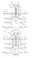
- FIGS. 17A-17C and 18illustrate embodiments of Z-directed signal delay line component.
- a Z-directed signal delay linecomprises a body having a signal conductor routed therein with the signal conductor made from one of a dielectric material, and a magnetic material that slows down signals that travel through the delay line.
- the signal conductorhas a length contained within the body and may be of the same length as the length of the body or may be longer in length than the length of the body. Connections to the signal conductor may be made via channels provided on the side surface of the Z-directed component or to conductive traces provided on the top and or bottom surfaces or by a combination of top and/bottom traces and channels.
- Z-directed component 700 Ahas a body 702 having conductive traces 703 a and 703 b on its top surface 702 t.
- delay line 704Disposed within body 702 a is delay line 704 comprised of a plurality of conductive legs comprising vertically oriented segments 704 a - 704 d extending along a portion of the length of body 702 a and connected by a plurality short horizontal bars 704 e in a serial fashion at their respective top and bottom ends (roughly approximating a W-shape) forming the delay line 704 in an undulating or a zigzag manner.
- the top ends of segments 704 a and 704 dare shown connected to conductive traces 703 a and 703 b respectively on the top surface 702 t of the body 702 a.
- the additional length of the conductor forming delay line 704 inserted into a signal pathcauses the signal travel a longer distance therefore delaying it.
- the connection to delay line 704may also be accomplished using a channel provided in the side 702 s of body 702 a either in combination with conductive traces on the top or bottom surfaces or in lieu of top and bottom conductive traces. Additional segments may be added to delay line 704 to increase the amount of delay.
- a Z-directed component delay line 700 Bhas a body 702 with conductive traces 703 t and 703 b on the top and bottom of body 702 b.
- delay line 705comprised of a plurality of horizontally disposed (as viewed in FIG. 16B ) C-shaped conductors 705 a - 705 d spaced apart from one another and serially connected by a plurality vertical leg segments 705 e.
- the C-shaped conductors 705 a - 705 dmay also be described as being disposed approximately parallel to the top or bottom surfaces, 702 t, 702 b of the body 702 and the leg segments 705 as approximately parallel to the side surface of the body.
- leg segments 705 e adjacent the top and bottom of body 702 bconnect to traces 703 c and 703 d on the top and bottom surfaces. Again the additional length of delay line 705 inserted into a signal path causes the signal travel longer, delaying it. If there is excessive capacitive coupling between adjacent C-shaped conductors then a shielding material (not shown) may be disposed within body 702 between adjacent C shaped conductors and grounded. It is expected that this should remove most of the parasitic affects of this geometry. The connections between adjacent C-shaped conductors are made such that the magnetic flux of one C-shaped conductor cancels the next. This reduces the magnetic coupling between the C-shaped conductors. Additional C-shaped conductors may be added to increase the delay. Alternatively, the delay line may be arranged in a spiral configuration.
- FIG. 17Cillustrates a programmable version of the Z-directed delay line of FIG. 17B .
- Z-directed delay 700 Chas body 702 b having top and bottom traces 703 t.
- Delay line 705 disposed within body 702 bis comprised of a plurality of serially connected C-shaped conductors as previously described.
- a shorting mechanism for the C-shaped conductorsis disposed within or on the body 702 b and may be comprised of at least one shorting bar. By selectably [selectively?] removing portions of the shorting bar between adjacent C-shaped conductor the amount of delay provided by Z-directed component delay line 700 C may be adjusted or programmed.
- shorting bars 708 , 709are shown and used to program the delay time of the part.
- shorting bars 708 , 709extend along the length of the body 702 b and tangentially contact each of the C-shaped conductors.
- the shorting bars 708 and 709are diametrically opposed to one another such that a line drawn between them would bisect each C-shaped conductor 705 a - 705 d. If the minimum delay is desired then shorting bars 708 , 709 are left in place. If the maximum delay is desired then shorting bars 708 , 709 are removed by drilling or etching the conductive material away.
- each PCBmay be tuned during functional testing to optimize the delay of signals to compensate for variation of other parameters in a design.
- One or more shorting barsmay also be used with Z-directed delay line 700 A by placing the shorting bar horizontally across the vertical conductor segments 704 a - 704 d as indicated by the line 710 .
- the time delaywould have to be adjusted prior to insertion of the part into a PCB.
- one or more channelsmay be provided as a shorting mechanism in lieu of shorting bars and by use of selective plating techniques in plating such Z-directed delay lines portions of delay lines 704 or 705 may be shorted together.
- variable delay line 730may be created by connecting any number of Z-directed delay line together by conductive traces on a PCB. These surfaces are shown as transparent to illustrate the connections.
- cylinders 750 , 760 , and 770Inserted in PCB 740 are cylinders 750 , 760 , and 770 which can represent either a Z-directed delay line, as illustrated in FIGS. 17A-17C , or a conductive plug or Z-directed signal pass through component and which are connected in series fashion by top and bottom conductive traces 780 t, 780 b as shown on the top and bottom surfaces 740 t, 740 b of PCB 740 .
- Cylinders 750 , 760 and 770may also be connected serially via conductive traces provided on internal layers of PCB 740 if present or by a combination of internal or external conductive traces. If cylinders 750 , 760 and 770 each represent a Z-directed delay line element, then total delay across delay line 730 may be changed by replacing a Z-directed component delay line elements with a Z-directed component signal pass through device, previously described, that introduces no significant delay or with another Z-directed component delay line having a greater delay.
- One advantage of this configurationis that no changes are required to the PCB layout design while still allowing the total signal delay to be adjusted.
- a Z-directed T filter and a Z-directed Pi filterare three port devices having an input conductor, output conductor and a ground conductor.
- T filtersare generally comprised of, for a low pass filter, two serial resistors connected between an input and an output with a capacitor connected between the resistors and to ground or, for a high pass filter, two serial capacitors connected between the input and an output and a resistor connected between the capacitors and to ground. Schematically these filters resemble the letter T.
- Pi filtershave one component connected between input and output with a second component connected between input and ground and a third component connected between the output and ground. The first component may be a resistor and the second and third component may be capacitors and vice versa. Inductors may also be used. These devices may be mounted in a Z-directed component in a similar fashion as the transistor shown FIG. 8 and 9 .
- FIGS. 19A-19Cillustrate cross-sectional views of alternate embodiments of Z-directed ferrite beads.
- the construction of these devicesis similar to that shown and described in FIGS. 5B-5H .
- a cylinder 1001 of magnetic materialhaving an opening through which conductor 1002 passes.
- the conductor 1002extends to the top and bottom surfaces of the body 1000 where it is electrically connected to top and bottom traces.
- the conductormay also be connected as previously described such as to a channel on the side surface of the body or two side channels etc.
- By varying the outside diameter cylinder 1001the magnetic properties are varied controlling the characteristics of the ferrite bead.
- cylinder 1001is contained within body 1000 but its outer circumference may also extend to the side surface of body 1000 . This construction creates a single conductor differential Z-directed ferrite bead.
- two conductors 1002 - 1 and 1002 - 2pass through two openings provided in cylinder 1001 in the body 1000 forming a two conductor differential mode Z-directed ferrite bead.
- the two parallel spaced apart conductors 1002 - 1 and 1002 - 2are enclosed by cylinder 1001 comprised of magnetic material.
- cylinder 1001comprised of magnetic material.
- the magnetic propertiesare varied controlling the characteristics of the ferrite bead.
- cylinder 1001is contained within body 1000 but its outer circumference may also extend to the side surface of body 1000 .
- FIG. 19CShown in FIG. 19C , is a two conductor common mode Z-directed ferrite bead that is substantially similar to a two conductor differential mode Z-directed ferrite bead but with both of the conductors 1002 - 1 , 1002 - 2 within the cylinder 1001 a passing through a common opening 1003 in the magnetic material forming cylinder 1001 a.
- the volume within opening 1003is not filled with magnetic material.
- the volumemay be left empty, i.e. air filled, or another nonmagnetic material may be used to filled the portion not filled by conductors 1002 - 1 , 1002 - 2 .
- FIGS. 20A and 20Billustrate a PCB 1101 having a multiplicity of internal layers 1102 having one or more conductive traces and a multiplicity of conductive surface traces 1103 , three of which are further designated as a, b and c, on outer surface 1104 . Conductive traces may be provided on both outer surfaces of PCB 1101 .
- Z-directed component 1105is mounted in mounting hole 1106 shown as a through hole. A channel 1107 of Z-directed component 1105 is shown aligned with circuit trace 1103 a.
- the channel 1107extends along the side surface 1105 from the top surface 1105 t to bottom surface 1105 b.
- the length of the channelmay be less the length of the body of the Z-directed component and may extend only from one of the top and bottom surfaces toward the other or may be disposed intermediate the top and bottom surfaces such as, for example, extending only between the two internal layers of PCB.
- Shown inserted into channel 1107is a compressive conductive member, such as rod 1109 .
- a compressive conductive membersuch as rod 1109 .
- a compressive conductive membersuch as rod 1109 .
- turning structuresuch as slot 1108 used to rotate Z-directed component 1105 into alignment with the desired surface trace 1103 .
- Other configurationssuch as a pair of holes or cross-shaped slots may also be used in lieu of slot 1108 .
- FIG. 20Bis a sectional view taken along line 20 B- 20 B of FIG. 20A with Z-directed component 1105 removed, a multiplicity of internal connection points 1110 - 1113 are shown.
- connection between trace 1103 a and connection point 1110is made as indicated by the dashed line interconnecting these two points.
- trace 1103 bwill be connected to connection point 1111 as indicated by the dashed line interconnecting these two points.
- trace 1103 cwill be connected to connection points 1112 and 1113 as indicated by the dashed line shown interconnecting these three points.
- the compressive conductive memberWhen the compressive conductive member is a rod it may have a diameter that is less than and preferably equal to or greater than the diameter of channel 1107 .
- compressive conductive rod 1109is shown having a diameter that is larger than the diameter of channel 1107 . This is done to ensure that compressive rod 1109 will be compressed when inserted in channel 1107 helping to ensure that compressive conductive rod 1109 will be retained within the body of Z-directed component 1105 due to the interference fit between the rod and channel. Further, as illustrated in FIG.
- channel 1107is positioned at the edge of Z-directed component 1105 so that the center line 1109 a of compressive conductive rod 1109 will positioned at a distance that is within or less than the radius R of Z-directed component 1105 while still allowing a strip 1109 s of the outer side surface of compressive conductive rod 1109 to extend beyond the side surface 1105 s of Z-directed component 1105 to make the desired electrical connections.
- This strip or portion 1109 s of the outer peripheryis exaggeratedly shown in FIG. 20D . It is expected that this will also aid in keeping Z-directed component 1105 inserted into PCB 1101 .
- Additional channels and compressive conductive rodsmay also be provided in Z-directed component 1105 and arranged about the periphery of Z-directed component 1105 as needed to meet the design requirements for the circuit forming a multi-pole switch.
- compressive rod 1109having a diameter that is less than the diameter of channel 1107 shims or other means such as raised portions in the channel wall inserted between the channel surface and the compressive conductive rod may be used to ensure the compressive conductive rod will have a portion extending beyond the side surface 1105 s of Z-directed component 1105 .
- channel 1120is generally triangular or trapezoidal in section with the open apex aligned with the side surface. Shown inserted in channel 1120 is a generally rectangular compressive conductive member 1122 which has pinched-in waist 1122 w caused by the sectional shape of channel 1120 . Member 1122 may also have a triangular section as well.
- Z-directed component 1105in this manner allows PCB 1101 to be configured with an identification indicia such as a serial number using a minimal number of components. Connections between the surface layers of PCB 1101 (either top surface, bottom surface or both) can also be made to inner layers by the use of a well provided in Z-directed component 1105 as previously described. Further one or more wells and one or more center conductors may be used to provide for a multiplicity of connections between and among the internal layers 1102 and surface layers of PCB 1101 .
- Z-directed component 1105may also be removably inserted into mounting hole 1106 allowing for it to be realigned similar to a single-gang or multi-gang rotary switch, depending on the number of layers in PCB 1101 .
- a slotmay be provided in one of the end surfaces of Z-directed component to allow it to be rotated by a screwdriver or other similar means.
- the top surface 1105 tmay have radial projections 1130 or a flange that can be used to prevent the Z-directed component from sliding out of the mounting hole when being rotated.
- the Z-directed component 1105may have a number of different circuits or values of components, indicated by dashed block 1115 in FIGS. 20C , incorporated into the body thereof and be used to connect one or more traces on a layer of the PCB (interior or exterior layer) with another one of more traces on the same or other surfaces in the PCB using channels or conductors as previously described.
- different circuitscan be selected by rotating the part to select which conductor(s) is/are bridged that have the desired circuit component between 2 or more connection points.
- one Z-directed componentmay have a range of resistive values therein that are selected by inserting the Z-directed component and aligning it with the desired conductive traces.
- the conceptmay be expanded to any combination of electronic components that will fit within the volume of the body of the Z-directed component along with the necessary conductive traces.
- FIG. 21A , 21 C, and 21 Dillustrate another configuration of an internal Z-directed component connector that can make the internal connections without the need for this back drilling process. This embodiment also illustrates the use of test paths with the body of the Z-directed component. This interior connector may be used anytime a plating well is not desired to the top or bottom layers of a PCB.
- a Z-directed component 1200has at least two recessed areas or pockets 1202 a, 1202 b, 1202 c, 1202 d on the side surface 1200 s that will contain a solder paste material (not shown) that will either expand or reflow when heated to make the desired connections.
- a conductor 1216 a, 1216 b, 1216 c, 1216 dis provided between top surface 1200 t and each of pockets 1202 a - 1210 d, respectively.
- the portions 1216 a 1 - 1216 d 1 of conductors 1216 a - 1216 d on surface 1200 tmay be used as test points by test probes as described herein.
- FIG. 21BShown in the FIG. 21B is a sectional view of a four-layer PCB 1210 having two internal layers 1211 a, 1211 b, each having two conductive signal traces 1212 a and 1212 b, 1212 c and 1212 d, respectively, provided at four internal locations in the wall 1214 w of mounting hole 1214 .
- trace 1212 ato trace 1212 c and trace 1212 b to trace 1212 d.
- Other numbers of internal layers and signal tracesmay also be connected in a similar fashion using an appropriately designed Z-directed component internal connector.
- Z-directed component 1200four correspondingly positioned pockets 1202 a - 1202 d are positioned on side surface 1200 s so that when Z-directed component 1200 is inserted into mounting hole 1214 these pockets will be adjacent to traces 1212 a - 1212 d respectively on internal layers 1211 a, 1211 b.
- the pocketsmay be interconnected by a variety of means as is known in the art. Two examples are illustrated in FIGS. 21A and 21C .
- Oneis a channel 1220 cut into side surface 1200 s interconnecting pockets 1202 b and 1202 d that may be filled with solder paste or into which the solder paste in the pockets will flow when heating of the PCB occurs. Additional channels interconnecting all of the pockets together can be provided and the pockets may be selectably interconnected by use of removable dams indicated by dashed lines 1224 provided in the channel 1220 . This permits the interconnections to be determined after the Z-directed connector has been fabricated. Where a connection is desired between two pockets the dam 1224 in the channel interconnecting these pockets would be removed.
- the other connectionmay be done by a conductor 1222 provided in the body 1200 b interconnecting pockets 1202 a and 1202 c. With this arrangement the manner of the interconnection would need to be predetermined so that the conductors are positioned between the desired interconnection points.
- test probes placed on test points 1216 a 1 - 1216 d 1For the illustrated pairs of connections only a single test point is needed for each pair of interconnected pockets; however it may be desired to have a test point for each connection pocket as shown.
- FIGS. 21C and 21Dshow Z-directed component internal connect 1200 having an optional multi-terminal component 1230 either embedded or formed within the body 1200 b.
- Component 1230may be an active or passive component may also be inserted in the connection path to the internal layers 1211 a, 1211 b of PCB 1210 .
- one terminal of component 1230is connected to top surface 1200 t of Z-directed component 1200 via conductor 1232
- a second terminalis shown connected to pocket 1202 a via conductor 1234
- a third terminal of component 1230is shown connected to pocket 1202 d via conductor 1236 .
- Components having more or less terminalsmay also be accommodated within Z-directed component 1200 depending on volume available for the internal component and conductors.
- test paths 1216 a - 1216 dmay not be present in some designs. However, the testing paths may be used with any of the Z-directed parts described herein to improve testability. Also the top and or bottom surface of this Z-directed component may have a conductive coating substantially coextensive with the surface to provide further shielding when the Z-directed component is installed and plated in a PCB.
- a Z-directed componentmay work best when partially inserted into the PCB.
- a Z-directed componentmay have a parameter, such as resistivity that can be controlled by the depth that it is inserted into the PCB.
- resistivitysuch as resistivity
- One examplewould be a resistor that normally has a fixed resistive value between the top and bottom surfaces by applying a uniform resistive film over the side surface of the body This is illustrated in FIGS. 22A and 22B illustrating a PCB 1300 having a Z-directed resistor 1320 inserted at two different depths into a mounting hole 1302 indicated by the dashed lines.
- the PCB 1300is illustrated as having signal traces 1303 , 1305 on one external surface, top surface 1300 t and signal traces 1307 , 1309 on the other external surface, bottom surface 1300 b. As shown in both figures Z-directed resistor 1320 interconnects signal trace 1303 to signal trace 1305 .
- Two internal layersare shown for PCB 1300 , a first voltage reference layer Vcc 1311 , and a second voltage reference layer GND 1313 .
- Side surface 1330 s of body 1330has two closed end or blind channels, 1332 , 1334 extending from top surface 1330 t. These blind channels could also both extend from the bottom surface 1330 b.
- a plateable strip 1340is shown disposed on side surface 1330 s of body 1330 between the top and bottom surfaces 1330 t, 1330 b. Disposed within body 1330 are conductors 1335 , 1336 electrically connected to respective ends of plateable strip 1340 . The other ends of conductors 1335 , 1336 are electrically connected to channels 1332 , 1334 .
- Line 1350indicates the position of top surface 1300 t with respect to body 1330 .
- Z-directed resistor 1320is inserted into mounting hole 1302 a depth D 1 where portion P 1 represent the portion of plateable strip 1340 below the top surface 1300 t of PCB 1300 and portion P 2 represents the portion of plateable strip 1340 above.
- the exposed side surface 1300 s above the top surface 1300 t along with portion P 2 of plateable strip 1340would be plated with copper shorting out the portion P 2 and reducing the overall resistance of Z-directed resistor 1320 .
- the channels 1332 , 1334are closed ended to prevent the plating material from shorting the two channels together.
- Z-directed resistoris shown inserted at a greater depth D 2 . Accordingly on plateable strip 1340 portion P 1 has increased and portion P 2 has decreased. At insertion depth D 2 and after plating has occurred, the overall resistive value of Z-directed resistor 1320 is greater than that when inserted at depth D 1 .
- This conceptmay be used with any passive element that can have its value adjusted by plating over part of a surface.
- a Z-directed inductorwherein portions of the windings are exposed along the length of the side surface.
- a Z-directed capacitorhaving stacked disks similar to those as shown in FIG. 15 but modified so as not to have the annular plate 617 connected to either of the side channels 604 , 608 . Instead one or more of the annular plates 617 would be electrically connected to a corresponding conductor disposed within the body 605 with the other end of the conductor being exposed on the side surface of the body 605 .
- a further exampleis a signal delay line such as that shown in FIG.
- FIGS. 7BAnother use for this partial insertion technique would be where different electronic functions exist in regions between the top and bottom surfaces of the body of the Z-directed component.
- multiple devices or circuitsmay be provided in the body 150 .
- Internal connectionsmay be provided to plateable pads provided in the side surface. The exposed pads would be shorted out by the copper plating in a similar way to the resistor example.
- a Z-directed componentcan be adjusted after the PCB has been manufactured.
- a circuit designmay call for a Z-directed component providing an optional function or feature to the circuit to be partially inserted into the PCB and make no connections at the time of manufacturing. Later if the Z-directed component is needed to add its new function to the circuit in the PCB it would be pushed into place while in the field.
- the strip used in a Z-directed variable value componentmay also have one or more etchable portions 1360 having a conductor connected to each end of the strip (see FIG. 22A ).
- the conductorsmay be internal to the body of the component, provided on an external surface or be a combination of external and internal connects as previously shown and described.
- the value of the Z-directed variable value componentwould be adjusted by selectively etching away etchable portions 1360 of the strip while still maintaining a signal path between the two end conductors. For example, if the strip were comprised of a resistive material, removal of some of this material by etching would decrease the value of the resistance. Depending on the material within the etchable portions the value of the component may increase or decrease as the material is etched away. Depending on the depth to which such a component is mounted in the PCB, fewer or more of the etchable portions would be exposed to etching.
- an insertion system 800comprising an orienting fixture 802 and ram plate 804 as shown in FIG. 23 .
- orienting fixture 802Positioned on orienting fixture 802 are one or more Z-directed components 806 .
- Orienting fixture 802 using locating surfaces or other indicia provided on Z-directed components 806 ram plateorients these components for insertion into PCB 850 shown positioned over orienting fixture 802 and having one or more mounting holes 852 for receiving Z-directed component 806 therein as previously described.
- PCB 850is held by a fixture not shown.
- mounting holes 852are through-holes and the depth D of the holes corresponds to the length L of Z-directed components 806 .
- the length Lmay be less than, equal to or greater than depth D allowing for recessed mounting, flush mounting or extended mounting.
- resist materialwill be needed to ensure that only those portions of the recessed surface that are to be plated will be plated and to avoid plating of the entire recessed surface.
- Ram plate 804is raised as indicated by arrow 860 inserting Z-directed components 806 into corresponding mounting holes 852 in PCB 850 through the bottom surface of PCB 850 .
- the ram platemay have cylinders that press each component 806 through the orienting fixture 802 into mounting holes 852 to the correct depth. These cylinders may be individually operated or any combination at one time.
- insertion equipmentthat orientates the part and inserts them into the PCB will be needed.
- pick and place equipmentmay also be used to insert a Z-directed component into a PCB.
- Such pick and place equipmentmay insert a Z-directed component from either the top or bottom surface of a PCB.
- a plunger devicewill be needed to press the Z-directed component into the PCB to the desired insertion depth.
- Z-directed componentsmay be press fit or glued in place in a PCB.
- the PCB and Z-directed component interfacecan include resist material to prohibit plating or seed material to help facilitate plating. Examples are shown in FIGS. 24 and 25 .
- a Z-directed component 900having a body 902 and two channels 904 a and 904 b extending alongside surface 902 s and a conductive top trace 906 is shown having a glue strip 910 or a glue dot 911 on side surface 902 s allowing Z-directed component 900 to adhere to the wall of a mounting hole in a PCB prior to plating.
- FIG. 24a Z-directed component 900 having a body 902 and two channels 904 a and 904 b extending alongside surface 902 s and a conductive top trace 906 is shown having a glue strip 910 or a glue dot 911 on side surface 902 s allowing Z-directed component 900 to adhere to the wall of a mounting hole in a PCB prior to plating.
- a Z-directed component 920having a body 922 and two channels 924 a and 924 b extending alongside surface 920 s and a conductive top trace 926 is shown having copper seed material 927 indicated by the horizontal lines on channels 924 a, 924 b conductive trace 926 with resist material 928 indicated by the angled lines on the remaining portions of side surface 902 s.
- Compliant materialsmay be used to keep plating material from migrating past desired locations.
- the seed coppermay be taken around the edge of a Z-directed component down the side surface to the surface of the PCB.
- Other surface mount partsmay be mounted over the part and may even have pads or balls to have surface mount parts connected directly to them.
- the ballsmay be attached directly to the top surface of a Z-directed component.
- Z-directed componentsmay also be contained in a tape and reel packaging material.
- a partcan be extracted using a pick and place vacuum head and be partially inserted in to a PCB.
- a cameracan then be used to check the orientation of the Z-directed component and the Z-directed component position adjusted before being fully inserted into the PCB.
Landscapes
- Engineering & Computer Science (AREA)
- Microelectronics & Electronic Packaging (AREA)
- Structures For Mounting Electric Components On Printed Circuit Boards (AREA)
- Structure Of Printed Boards (AREA)
Abstract
Description
- This patent application is related to U.S. patent applications Ser. No. ______ (Attorney Docket No. 2008-0295.01) entitled “Z-directed Components for Printed Circuits Boards”; Ser. No. ______ (Attorney Docket No. 2009-0117.00) entitled “Z-directed Pass-Through Components for Printed Circuits Boards”; Ser. No. ______ (Attorney Docket No. 2009-0118.00) entitled “Z-directed Capacitor Components for Printed Circuits Boards”; Ser. No. ______ (Attorney Docket No. 2009-0120.00) entitled “Z-directed Filter Components for Printed Circuits Boards”; Ser. No. ______ (Attorney Docket No. 2009-0121.00) entitled “Z-directed Ferrite Bead Components for Printed Circuits Boards”; Ser. No. ______ (Attorney Docket No. 2009-0122.00) entitled “Z-directed Switch Components for Printed Circuits Boards”; Ser. No. ______ (Attorney Docket No. 2009-0123.00) entitled “Z-directed Connector Components for Printed Circuits Boards”; Ser. No. ______ (Attorney Docket No. 2009-0124.00) entitled “Z-directed Variable Value Components for Printed Circuits Boards”; each filed MONTH DAY, 2009 and all assigned to the assignee of the present application.
- None.
- None.
- 1. Field of the Invention
- The present invention relates electronic components, and more particularly to those for insertion into a printed circuit board and methods of assembly.
- 2. Description of the Related Art
- Printed Circuit Board (“PCB”) manufacturing, primarily uses two types of components. The first type is pin through-hole parts that use metallic leads that are soldered into a plated through-hole in the PCB. The second type of component is a surface mount part that sits on the surface of a PCB and it attached by soldering to pads on the surface. As densities of components have increased and higher frequencies of operation are used, some circuits' designs have become very difficult to achieve. The presented invention improves the component densities and frequencies of operation.
- Currently resistors can be embedded between layers of a PCB by applying a resistive material between two copper traces after the etching step in the manufacturing process. A typical 4 layer PCB is made up of two assemblies that are each two layer PCBs. These are glued together with a material to become the completed assembly. The resistive area can be applied to any layer making it possible to have the resistive elements on the interior layers. However this approach is more time consuming and makes changes difficult to implement. The present invention removes these difficulties by allowing for insertion of the part to occur after the multilayered PCB is assembled.
- A Z-directed component signal delay line for mounting in a PCB having a mounting hole having a depth D therein comprises of an insulative body having a top surface, a bottom surface and side surface, a cross-sectional shape that is insertable into the mounting hole in the PCB and a length L, a signal conductor contained within the body between the top and bottom surface for passing a signal therethrough and having a length that is equal to or greater than length L; and a pair of conductive traces provided on one of the surfaces of the body, a conductive trace electrically connected to each end of the signal conductor. The signal conductor is made from one of a dielectric material and a magnetic material. The signal conductor has a length that is longer than the length L. A pair of conductive traces are provided on one of the top surface of the body and the bottom surface of the body. Alternatively one of the pair of conductive traces is provided on the top surface of the body and the other of the pair of conductive traces is provided on the bottom surface of the body. In another form at least one of the pair of conductive traces comprises a channel in the side surface of the body. The signal conductor may have a plurality of legs connected in zigzag pattern. In a further form, a shorting bar positioned across at least two adjacent legs of the signal conductor is provided.
- In another form the signal conductor comprises a plurality of C-shaped conductors disposed approximately parallel to one of the top and bottom surfaces of the body and spaced apart from one another; and a plurality of leg segments disposed approximately parallel to the side surface of the body, the plurality of C-shaped conductors serially connected by the plurality of vertical leg segments with the ends of the leg segments adjacent the top and bottom surfaces of the body connected to the respective traces on the top and bottom surfaces of the body. Here shielding material disposed within the body between adjacent C-shaped conductors can be provided. In a further a shorting mechanism for electrically shorting together at least two adjacent C-shaped conductors is provided.
- In a still further form a programmable signal delay line circuit comprises a PCB having a plurality of mounting holes, each having a depth D therein and a plurality of conductive traces interconnecting the mounting holes in a serial fashion; and a plurality of Z-directed signal delay line components, each signal delay line component insertable into one of the mounting holes and electrically interconnected in a serial fashion. Each signal delay line comprises an insulative body having a top surface, a bottom surface and side surface, a cross-sectional shape that is insertable into the mounting hole in the PCB and a length L; a signal conductor contained within the body between the top and bottom surface for passing a signal therethrough and having a length that is greater than length L; and a pair of conductive traces provided one of the surfaces of the body, a conductive trace electrically connected to each end of the signal conductor, each of the pair of conductive traces electrically interconnected to a respective one of the plurality of conductive traces of the printed circuit board. The signal delay is adjusted by replacing at least one of the plurality of Z-directed signal delay line components with a signal pass through device comprising an insulative body having a top surface, a bottom surface and side surface, a cross-sectional shape that is insertable into the mounting hole in the PCB and a length L; a conductor extending through the length of the body between the top and bottom surface for passing a signal therethrough; and a pair of conductive traces, one on each of the top and bottom surfaces electrically connected to an end of the conductor adjacent thereto and extending therefrom to an edge of the body.
- The above-mentioned and other features and advantages of the various embodiments of the invention, and the manner of attaining them, will become more apparent will be better understood by reference to the accompanying drawings, wherein:
FIG. 1 is an illustration of one embodiment of a Z-directed component;FIG. 2 is an illustrates the internal arrangement of elements comprising one embodiment of the Z-directed component ofFIG. 1 ;FIGS. 3A-3F illustrate various shapes for the body of a Z-directed component;FIGS. 4A-4C illustrate various channel configurations for a Z-directed component;FIGS. 5A-5H illustrate various channel and conductor configurations for the body of a Z-directed component;FIGS. 6A-6D illustrate various orienting locating or connection features of a Z-directed component;FIGS. 7A and 7B illustrate a Z-directed component having O-rings for connecting to internal layers of a PCB and having a body having regions comprised of similar and or dissimilar materials;FIG. 8 illustrates various elements or electronic components such as a resistor, diode, capacitor that may be provided within the body of a Z-directed component in series with a conductor;FIG. 9 illustrates a Z-directed component having a 3-terminal transistor connected to two conductors;FIG. 10 illustrates an alternate embodiment of a Z-directed component having a 3-terminal transistor connected to a conductor and a plated channel;FIG. 11 illustrates a cross-sectional view of the embodiment of a Z-directed component flush mounted within a PCB shown inFIG. 12 ;FIG. 12 illustrates a top view of the PCB and the Z-directed component ofFIG. 11 showing the conductive traces and connections to the Z-directed component;FIG. 13 illustrates ground loops for the Z-directed component ofFIGS. 11 and 12 with the Z-directed component further comprising with a decoupling capacitor within the body of the Z-directed component;FIG. 14 is an illustration of a Z-directed component for transferring a signal trace from one internal layer of a PCB to another internal layer of that PCB;FIG. 15 is an illustration of one embodiment of a Z-directed capacitor comprising semi-cylindrical sheets;FIG. 16 is an exploded view illustration of another embodiment of a Z-directed capacitor comprising stacked discs;FIGS. 17A-17C illustrate alternate embodiments of a Z-directed delay line with transparent surfaces to display connections;FIG. 18 illustrates a programmable Z-directed delay line circuit having multiple Z-directed delay lines with transparent surfaces to display connections;FIGS. 19A-19C illustrate sectional views of a single conductor differential Z-directed ferrite bead, a 2 conductor differential mode Z-directed ferrite bead, and a 2 conductor common mode Z-directed ferrite bead;FIGS. 20A and 20B illustrate a Z-directed switch component that can be rotated to connect predetermined circuit paths in a PCB;FIG. 20B is a sectional illustration of the PCB taken alongline 20B-20B ofFIG. 19A with the Z-directed switch component removed to show internal connection points of the PCB;FIG. 20C is an illustration of the Z-directed switch component ofFIG. 20A having an internal electronic component;FIG. 20D is a top view of the Z-directed switch component ofFIG. 20C showing alternate configurations of the channel shapes and conductive member and radial projections;FIGS. 21A-21D illustrate a Z-directed component utilized for making internal connections between traces on different internal layers or between traces on a given internal layer of a PCB along with an additional feature of a testing path for checking the connections;FIGS. 22A and 22B illustrate the use of a plateable side strip and partial insertion of Z-directed components to alter value or function of the Z-directed component;FIG. 23 is an illustration of a system for inserting Z-directed components into a PCB;FIG. 24 is an illustration of a Z-directed component having a glue strip and a glue dot for mounting of the Z-directed component in a PCB; andFIG. 25 is an illustration of a Z-directed component showing copper seed material and resist material used when plating a Z-directed component.- The present invention will now be described more fully hereinafter with reference to the accompanying drawing figures, in which some, but not all embodiments of the invention are shown. It is to be understood that the invention is not limited in its application to the details of construction and the arrangement of components set forth in the following description or illustrated in the drawings. The invention may be embodied in many different forms and should not be construed as limited to the embodiments set forth herein; rather, these embodiments are provided so that this disclosure will satisfy applicable legal requirements.
- The phraseology and terminology used herein is for the purpose of description and should not be regarded as limiting. The use of “including,” “comprising,” or “having” and variations thereof herein is meant to encompass the items listed thereafter and equivalents thereof as well as additional items. Unless limited otherwise, the terms “connected,” “coupled,” and “mounted,” and variations thereof herein are used broadly and encompass direct and indirect connections, couplings, and mountings. In addition, the terms “connected” and “coupled” and variations thereof are not restricted to physical or mechanical connections or couplings.
- As described in subsequent paragraphs, the specific mechanical configurations illustrated in the drawings are intended to exemplify embodiments of the invention and that other alternative mechanical configurations are possible.
- This specification describes a family of components that are intended to be embedded or inserted into a PCB. These components are termed Z-directed components and have been modeled and basic prototypes of many of the components described herein, but lacking the surface channels, were made to establish proof of concept. Not all embodiments described herein have been constructed. An overview of how Z-directed components are intended to be formed is presented initially followed by configurations for Z-directed component designs including but not limited to capacitors, delay lines, transistors, switches, and connectors. This is followed by techniques believed to be useful for assembling PCBs with Z-directed components. Z-directed components occupy less space on the surface of a PCB and for high frequency circuits (e.g. clock rates greater than 1000 MHz) allow for higher frequency of operation
- As used here in an X-Y-Z frame of reference is used. The X and Y axes describe the plane of a printed circuit board. The Z-axis describes a direction perpendicular to the plane of the circuit board. The top surface of the PCB has a zero Z- value. A component with a negative Z-direction value indicates that the component is inserted into the top surface of the PCB. Such a component may be above (extend past), flush with, or recessed below either the top surface and/or the bottom surface of the PCB. A component having both a positive and negative Z-direction value indicates that the component is partially inserted into the surface of the PCB. Z-directed components are intended to be inserted into a hole or recess in a printed circuit board. Depending on its shape and length more than one Z-directed component may be inserted into a single mounting hole in the PCB, such as being stacked together or positioned side by side. The hole may be a through hole (a hole from the top surface through to the bottom surface) or a well (an opening or recess through either the top or bottom surface into an interior portion or internal layer of the PCB.
- As described herein the Z-directed components are illustrated as being inserted into the top surface of the PCB. For a PCB having conductive traces on both external layers, one external layer is termed the top surface and the other the bottom surface. Also where only one external layer has conductive traces, that external surface is referred to as the top surface. The Z-directed component is referred to as having a top surface, a bottom surface and a side surface. The references to top and bottom surfaces of the Z-directed component conform to the convention used to refer to the top and bottom surfaces of the PCB. The side surface of a Z-directed component is in the Z-direction and would be adjacent to the wall of the mounting hole in the PCB which is also in the Z-direction. This use of top, bottom and side should not be taken as limiting how a Z-directed component may be mounted into a PCB. Although the components are described herein as being mounted in a Z-direction, this does not mean that such components are limited to being inserted into a PCB only along the Z-axis. Z-directed components may be mounted normal to the plane of the PCB from the top or bottom surfaces or both surfaces, mounted at an angle thereto or, depending on the thickness of the PCB and the dimensions of the Z-directed component and even inserted into the edge of the PCB between to the top and bottom surfaces of the PCB.
- The Z-directed components may be made from various combinations of materials commonly used in electronic components. The signal connection paths will be made from conductors which are materials that have high conductivity. Conducting materials include, but are not limited to, copper, gold, aluminum, silver, tin, lead and many others. Z-directed components will have areas that need to be insulated from other areas by using materials that have low conductivity like plastic, glass, FR4 (epoxy & fiberglass), air, mica, ceramic and others. A Z-directed component that is constructed as a resistor requires materials that have properties that are between a conductor and insulator which have a finite amount of resistivity which is the reciprocal of conductivity. Materials like carbon, doped semiconductor, nichrome, tin-oxide and others are used for their resistive properties. Capacitors are typically made of two conducting plates separated by an insulating material that has a high permittivity (dielectric constant). Permittivity is a parameter that shows the ability to store electric fields in the materials like ceramic, mica, tantalum and others. Inductors are typically made of coils of wires or conductors wrapped around a material with high permeability. Permeability is a parameter that shows the ability to store magnetic fields in the material which are iron and alloys like nickel-zinc, manganese-zinc, nickel-iron and others. Transistors and FET are electronic devices that are made from semiconductors that
- The PCB which uses a Z-directed component may be constructed to have a single conductive layer or multiple conductive layers as is known. The PCB may have conductive traces on the top surface only, on the bottom surface only, on both the top and bottom surfaces. In addition one or more intermediate internal conductive trace layers may also be present in the PCB.
- Connections between a Z-directed component and the traces in or on a PCB may be accomplished by soldering techniques, screening techniques, extruding techniques or plating techniques as are known in the art. Depending upon application, solder pastes and component adhesives may be used. In some configurations, compressive conductive members may be used to interconnect a Z-directed component to conductive traces found on the PCB.
- The most general form a Z-directed component comprises a body having a top surface, a bottom surface and a side surface, a cross-sectional shape that is insertable into a mounting hole of a given depth D within a PCB with a portion of the body comprising an insulator. All of the embodiments described herein for Z-directed components are based on this general form.
FIGS. 1 and 2 show an embodiment of a Z-directed component. There Z-directedcomponent 10 comprises a generallycylindrical body 12 having atop surface 12t,abottom surface 12b,aside surface 12s,and a length L generally corresponding to the depth D of the mounting hole. The length L can be less than, equal to or greater than the depth D. In the former two cases, Z-directedcomponent 10 would in one case be below at least one of the top and bottom surfaces of the PCB and in the other it would be flush with the two surfaces of the PCB. Where length L is greater than depth D, Z-directedcomponent 10 would not be flush mounted. However with this non-flush mount, Z-directedcomponent 10 would be capable of being used to interconnect to another component or another PCB that is positioned nearby. The mounting hole is typically a through-hole extending between the top and bottom surfaces of the PCB but it may also be a blind hole. When recessed below the surface of the PCB additional resist areas may be required in the hole of the PCB to keep from plating the entire circumferential area around the hole.- Z-directed
component 10 in one form may have at least oneconductor 14 extending through the length ofbody 12. At the top and bottom ends14tand14bofconductor 14 top and bottom conductive traces16t,16bare provided on the top and bottom end surfaces12t,12bofbody 12 and extend from respective ends of theconductor 14 to the edge of Z-directedcomponent 10. In thisembodiment body 12 comprises a non-conductive material. Depending on its function,body 12 of Z-directedcomponent 10 may be made of variety of materials having different properties. These properties include being conductive, resistive, magnetic, dielectric, or semiconductive or various combinations of properties as described herein. Examples of materials that have the properties are copper, carbon, iron, ceramic or silicon, respectively.Body 12 of Z-directedcomponent 10 may also comprise a number of different networks needed to operate a circuit that will be discussed later. - One or more longitudinally extending channels or wells may be provided on the side surface of body of Z-directed
component 10. The channel may extend from one of the top surface and the bottom surface ofbody 12 toward the opposite surface. As illustrated two concave wells orchannels component 10 extending the length ofbody 12. When plated or soldered, these channels allow electrical connections to be made to Z-directedcomponent 10, through the PCB, as well as to internal conductive layers within the PCB. The length of thechannels body 12. FIG. 2 shows the same component as inFIG. 1 but with all the surfaces transparent. Theconductor 14 is shown as a cylinder extending through the center of Z-directedcomponent 10. Other shapes may also be used forconductor 14.Traces body 12 is a conductor that connects thetop trace 16tto thebottom trace 16b.Whiletraces - Body shape may be any shape that can fit into a mounting hole in a PCB.
FIGS. 3A-3F illustrate possible body shapes for a Z-directed component.FIG. 3A shows a triangularcross-sectional body 40;FIG. 3B a rectangular crosssectional body 42;FIG. 3C a frusto-conical body 44;FIG. 3D an ovate cross sectionalcylindrical body 46; andFIG. 3E acylindrical body 48.FIG. 3F is a steppedcylindrical body 50 where oneportion 52 has a larger diameter than anotherportion 54. With this arrangement the Z-directed component may be mounted on the surface of the PCB while having a section being inserted into the mounting hole provided in the PCB. The edges of Z-directed component may be beveled to help with aligning the Z-directed component for insertion into a through-hole in a PCB. Other shapes and combinations of those illustrated may also be used for a Z-directed component. - For a Z-directed component, the channels for plating can be of various cross-sectional shapes and lengths. The only requirement is that plating or solder material make the proper connections to the Z-directed component and corresponding conductive traces in or on the PCB.
Channels FIGS. 4A-4C illustrate three channel shapes. InFIG. 4A V-shapedchannels 60 are shown. InFIG. 4B , U- or C-shapedchannels 62 are shown. InFIG. 4C , wavy or irregular cross-sectional channel shapes65 are shown. - The numbers of layers in a PCB varies from being single sided to being over 22 layers and may have different overall thickness that range from less than 0.051 inch to over 0.093 inch or more. Where a flush mount is desired the length of the Z-directed component will depend on of the thickness of the PCB into which is intended to be inserted. The Z-directed component's length may also vary depending of the intended function and tolerance of a process. The preferred lengths will be where the Z-directed component is either flush the surfaces or extends slightly beyond the surface of the PCB. This would keep the plating solution from plating completely around the interior of the PCB hole that may cause a short in some cases. It is possible to add a resist material around the interior of a PCB hole to only allow plating in the desired areas. However, there are some cases where it is desired to completely plate around the interior of a PCB hole above and below the Z-directed component. For example if the top layer of the PCB was a Vcc plane and the bottom layer is a GND plane then a decoupling capacitor would have lower impedance if the connection used a greater volume of copper to make the connection.
- There are number of features that can be added to a Z-directed component to create different mechanical and electrical characteristics. The number of channels or conductors can be varied from zero to any number that can maintain enough strength to take the stresses of insertion, plating, manufacturing processes and operation of the PCB in its intended environment. The outer surface of a Z-directed component may have a coating that glues it in place. Flanges or radial projections may also be used to prevent over or under insertion of a Z-directed component into the mounting hole, particular where the mounting hole is a through-hole. A surface coating material may also be used to promote or impede migration of the plating or solder material.
- A Z-directed component may take on several roles depending on the number of ports or terminals needed to make connections to the PCB. Some possibilities are shown in
FIGS. 5A-H .FIG. 5A is a Z-directed component configured as 0-port device 70A used as a plug so that if a filter or a component is optional then the plug stops the hole from being plated. After the PCB has been manufactured, the 0-port device 70A may be removed and another Z-directed component may be inserted, plated and connected to the circuit.FIGS. 5B-5H illustrate various configurations useful for multi-terminal devices such as resistor, diode, transistor, clock circuit.FIG. 5B shows a 1-port or single signal Z-directedcomponent 70B having aconductor 71 connected to top and bottom conductive traces72t,72b.FIG. 5C shows a 1-port 1-channel Z-directedcomponent 70C where one plated well orchannel 73 is provided in addition toconductor 71 and top and bottom conductive traces72tand72b.FIG. 5D shows a Z-directedcomponent 70D having twowells conductor 71 and top and bottom traces72t,72b.The Z-directedcomponent 70E ofFIG. 5E has threewells conductor 71 and top and bottom traces72t,72b.FIG. 5F shows Z-directedcomponent 70F having twoconductors component 70F is a two signal device to be primarily used for differential signaling.FIG. 5G shows a Z-directedcomponent 70G having one well73 and twoconductors FIG. 5H shows Z-directedcomponent 70H having oneconductor 71 with top and bottom traces72t,72band a blind well or partial well78 extending from the top surface along a portion of the side surface that will allow the plating material or solder to stop at a given depth. For one skilled in the art, the number of wells and signals is only limited by the space, required well size and conductor sizes. - In most cases Z-directed components will need to be orientated correctly when inserted into a PCB. Accordingly, locating or orienting features and connections features may be provided.
FIGS. 6A-6C illustrate examples of such locating features whileFIG. 6D illustrate a connection feature. InFIG. 6A , Z-directedcomponent 80A has a V-notch 81 on an end surface extending radially outward. InFIG. 6B , Z-directedcomponent 80B has arecess 83 on an end surface of Z-directedcomponent 80B having an orientingsurface 84.FIG. 6C shows Z-directedcomponent 80C having an axial projection, peg85, extending axially outward from an end surface and having an orientingsurface 86. An ink mark or other visual or magnetic indicator on an end surface or on the side of a Z-directed component may also be used to orient a Z-directed component such as when using a camera. - As shown in
FIG. 6D , Z-directedcomponent 80D may be fitted with a connection feature such as a conductive pad, a spring loaded style pogo-pin or even asimple spring 88 that may be used to add an additional electrical connection (such as frame ground) point to a printed circuit board.Spring 88 is illustrated as being connected toconductor 89 of Z-directedcomponent 80D. FIGS. 7A and 7B illustrate another configuration for a Z-directed component utilizing O-rings for use in a PCB having a top and bottom conductive layer and at least one internal conductive layer. Z-directedcomponent 150 is shown having on itstop surface 150t,a locatingfeature 152 and conductivetop trace 154textending betweenconductor 156 and the edge ofbody 150don itstop surface 150t.(A conductive bottom trace not shown is provided on the bottom surface).Conductor 156 extends through a portion of thebody 150das previously described. Located on theside surface 150sofbody 150dis a least one semi-circular channel or grove. As shown a pair of axially spaced apartcircumferential channels rings channels side surface 150sof thebody 150d.O-rings - O-
rings rings component 150 within the mounting hole. Theregion 162 ofbody 150dintermediate O-rings regions body 150doutside of the O-rings. For example if the material ofregion 162 is of a resistive material and O-rings Regions region 162. Forexample region 164 may be resistive,region 162 capacitive andregion 166 inductive. Each of these regions can be electrically connected to the adjoining layers of the PCB.Further conductor 156 and traces154t,154bdo not need to be provided. So for the illustrated construction, between the top layer of the PCB and the first internal layer from the top, a resistive element may be present inregion 164, a capacitive element between the first internal layer and the second internal layer inregion 162 and an inductive element between the second internal layer and the bottom layer of the PCB inregion 166. Accordingly, for a signal transmitted from an internal trace contacting conductive O-ring 160aand to a second internal trace contacting conductive O-ring 160b,the signal would see an inductive load. The material forregions - In
addition regions electronic components FIGS. 7-9 . Also as illustrated for component171 a component may be found within one or more regions within the body of a Z-directed component. Internal connections may be provided from embedded components to O-rings side surface 150s. - The various embodiments discuss for a Z-directed component are meant to be illustrative and not limiting. A Z-directed component may be made of a bulk material that performs a network function or may have other parts embedded into its body.
- Given that a Z-directed component may be a multi-terminal device, it is clear that it may be used to perform, but not limited to, the following functions: transmission line; delay line; T filter; decoupling capacitor; inductor; common mode choke; resistor; differential pair pass through; differential ferrite bead; diode; ESD protection devices (varistors). Also note that may combinations by be put together within one component.
FIG. 8 illustrates various configurations for a conductor in a Z-directed component. As shownconductor 90 has aregion 92 intermediate the ends comprising a material having properties selected from a group comprising conductive, resistive, magnetic, dielectric, capacitive or semiconductive properties and combinations thereof. These materials form a variety of components. Additionally a component may be inserted or embedded intoregion 92 with portions of the conductor extending from the terminals of the component. Acapacitor 92amay be provided inregion 92. Similarly adiode 92b,atransistor 92c,amosfet 92d,azener diode 92e,aninductor 92f,asurge suppressor 92g,aresistor 92h,adiac 92iand avaractor 92jand combinations of these items are further examples of materials that provided inregion 92 ofconductor 90. Whileregion 92 is shown as being centered within theconductor 90 it is not limited to that location.- For multi-terminal devices such as three
terminal devices transistor 92cormosfet 92d,or integratedcircuit 92k,or a transformer92l,one portion of the conductor may be between the top surface trace and to a first terminal of the device, the other portion of the conductor between the bottom surface trace and a second terminal of the device. For additional device terminals, additional conductors may be provide in the body of the Z-directed component to allow electrical connection to the remaining terminals or additional conductive traces may be provided within the body of the Z-directed component between the additional terminals and channels on the side surface of the body of a Z-directed component allowing electrical connection to an external conductive trace. Various connection configurations to a multiple terminal device may be used in a Z-directed component. FIGS. 9 and 10 illustrate two exemplary connection configurations for a transistor. InFIG. 9 , a Z-directed component,100, similar to that shown inFIG. 5F , having twoconductors body 105.Conductor 102 comprising atop portion 102t,abottom portion 102band anintermediate region 102iwhereintransistor 108 is provided. The base108boftransistor 108 is electrically connected to thetop portion 102tofconductor 102 while theemitter 108eis connected to thebottom portion 102bofconductor 102. Thecollector 108cis connected toconductor 104 viaconductive trace 109. InFIG. 10 , Z-directedcomponent 110, similar to that shown inFIG. 5C , hasbody 115 includingconductor 112 andchannel 114.Conductor 112 comprises atop portion 112t,abottom portion 112b,and anintermediate region 112iwhereintransistor 118 is provided. The base118boftransistor 118 is electrically connected to thetop portion 112tofconductor 112 while theemitter 118eis connected to thebottom portion 112bofconductor 112. Thecollector 118cis connected byconductive trace 119 to channel114 which is plated. The examples shown inFIGS. 8 and 9 may be extended to additional channels and conductors allowing for use of multi-terminal circuits. The connections are intended only to illustrate how connections to a multi-terminal component may be accomplished and are not meant to limit how a transistor may be connected within a Z-directed component.- Reference is now made to
FIGS. 11 and 12 illustrating a Z-directed component termed a signal pass-through that is used for passing a signal trace from the top surface of a PCB to the bottom surface.FIG. 11 shows a sectional view taken along line11-11 inFIG. 12 of aPCB 200 having 4 conductive planes or layers comprising, from top to bottom, a ground (GND) plane ortrace 202, a voltagesupply plane Vcc 204, a secondground GND plane 206 and a third ground GND plane or trace208 separated by nonconductive material such as a phenolic plastic such as FR4 which is widely used as is known in the art.PCB 200 may be used for high frequency signals. The top and bottom ground planes or traces,202 and208 respectively, on the top andbottom surfaces PCB 200 are connected to conductive traces leading up to Z-directedcomponent 220. A mountinghole 216 having a depth D in a negative Z direction is provided inPCB 200 for the flush mounting of Z-directedcomponent 220. Here depth D corresponds to the thickness ofPCB 200; however depth D may be less than the thickness ofPCB 200 creating a blind hole therein. Mountinghole 216, as illustrated, is a through-hole that is round in cross-section to accommodate Z-directedcomponent 220 but may have cross sections to accommodate the insertion of Z-directed components having other body configurations. In other words, mounting holes are sized so that Z-directed components are insertable therein. For example, a Z-directed component having a cylindrical shape may be inserted into a square mounting hole and vice versa. In the cases where Z-directed component does not make a tight fit, resist materials will have to be added to the areas of the component and PCB where copper plating is not desired. - Z-directed
component 220 is illustrated as a three lead component that is flush mounted with respect to both thetop surface 212 andbottom surface 214 ofPCB 200. Z-directedcomponent 220 is illustrated as having a generallycylindrical body 222 of a length L. A center conductor or lead224, illustrated as being cylindrical, is shown extending the length ofbody 222. Two concave wells orchannels component 220 extending the length ofbody 222.Channels component 220 from various layers ofPCB 200. As shown the ground plane traces onlayers PCB 100 are electrically connected tochannels Vcc plane 204 does not connect to Z-directedcomponent 220 as shown by thegap 219 betweenVcc plane 204 andwall 217 of mountinghole 216. FIG. 12 illustrates a top view of Z-directedcomponent 220 inPCB 200. Threeconductive traces wall 217 of mountinghole 216. As illustrated,trace 252 serves as a high-frequency signal trace to be passed from thetop surface 212 to thebottom surface 214 ofPCB 200 via Z-directedcomponent 220. Conductive traces250 and254 serve as ground nets. Center lead orconductor 224 is electrically connected to trace252 on thetop surface 212 ofPCB 200 by atop trace 245 andplating bridge 230.Top trace 245 on the top surface of Z-directedcomponent 220 extends from thetop end 224tofconductor 224 to the edge of Z-directedcomponent 220. Although not shown, the bottom side of Z-directedcomponent 220 andbottom surface 214 ofPCB 200 is configured in a similar arrangement of traces as shown ontop surface 212 ofPCB 200 illustrated inFIG. 12 . A bottom trace on the bottom surface of Z-directedcomponent 220 extends from bottom ofconductor 224 to the edge of Z-directedcomponent 220. A plating bridge is used to make the electrical connection between the bottom trace and another high frequency signal trace provide on the bottom surface ofPCB 200. The transmission line impedance of the Z-directed component can be adjusted to match the PCB trace impedance by controlling the conductor sizes and distances between each conductor which improves the high speed performance of the PCB.- During the plating process,
wells wall 217 of mountinghole 216 andchannels top surface 212 to thebottom surface 214 electrically interconnecting traces250 and254, respectively tochannels component 220 and also to similarly situated traces provided on thebottom surface 214 ofPCB 200 interconnecting ground planes or traces202,206 and208. The plating is not shown for purposes of illustrating the structure. In thisembodiment Vcc plane 204 does not connect to Z-directedcomponent 220. - One of the challenges for high frequency signal speeds is the reflections and discontinuities due to signal trace transmission line impedances changes. Many PCB layouts try to keep high frequency signals on one layer because of these discontinuities caused by the routing of signal traces through the PCB. Standard vias through a PCB have to be spaced some distance apart which creates high impedance between the signal via and the return signal via or ground via. As illustrated in
FIGS. 11 and 12 , the Z-directed component and the return ground or signals have a very close and controlled proximity that allows essentially constant impedance from thetop surface 212 to thebottom surface 214 ofPCB 200. - A Z-directed signal pass through component may also comprise a decoupling capacitor that will allow the reference plane of a signal to switch from a ground plane, designated GND, to a voltage supply plane, designated VCC, without having a high frequency discontinuity.
FIG. 13 shows a cross-sectional view of a typical 4-layer PCB 300 with asignal trace 302 transferring between thetop layer 304 and thebottom layer 306. Z-directedcomponent 310, similar to that shown inFIG. 5D , havingbody 312 connectssignal trace 302 through center conductor314. Z-directedcomponent 310 also comprises platedchannels side surface 312sof thebody 312. The top314tand bottom314bof conductor314 are connected toconductive traces body 312. These in turn are connected to signaltrace 302 via top and bottom plating bridges330tand330b.Channels GND plane 332 andVcc plane 334, respectively. Connection points336 and338, respectively, illustrate this electrical connection. Schematically illustrateddecoupling capacitor 350 is internal tobody 312 and is connected betweenchannels Decoupling capacitor 350 may be a separate capacitor integrated into thebody 312 of Z-directedcomponent 310 or it can be formed by fabricating a portion of thebody 312 of Z-directedcomponent 310 from the required materials with dielectric properties between conductive surfaces. - The path for
signal trace 302 is illustrated with diagonal hatching and can be seen to run fromtop layer 304 tobottom layer 306.GND plane 332 andchannel 316 are electrically connected at336 with the signal path return indicated by thedark stippling 362.Vcc plane 334 andchannel 318 are electrically connected at338 with the signal path return indicated by thelight stippling 364 As is known in the art where a signal plane or trace is not to be connected to the inserted part those portions are spaced apart from the component as shown at370. Where a signal plane or trace is to be connected to an inserted component, the signal plane or trace is provided at the wall or edge of the opening to allow the plating material or solder to bridge therebetween as illustrated atpoints - The vertically hatched
portion 380 shows the high speed loop area between the signal trace and return current path described by thesignal trace 302 and theGND plane 332 orVcc plane 334. Thesignal trace 302 on thebottom surface 306 is referenced topower plane Vcc 334 that is coupled to theGND plane 332 throughdecoupling capacitor 350. This coupling between the two planes will keep the high frequency impedance close to constant for the transition from one return plane to another plane of a different DC voltage. - Internally mounting Z-directed components in a PCB greatly facilitate the PCB technique of using outer ground planes for EMI reduction. With this technique, signals are routed on the inner layers as much as possible.
FIG. 14 illustrates one embodiment of this technique.PCB 400 is comprised of, from top to bottom,top ground layer 402,internal signal layer 404,internal signal layer 406 andbottom ground layer 408. Ground layers402 and408 are on the top andbottom surfaces PCB 400. A mountinghole 410 shown as a through-hole extends between the top andbottom surfaces component 420 is shown flush mounted inPCB 400. Z-directedcomponent 420 comprisesbody 422 having acenter region 424 intermediate the top422tand bottom422bofbody 422 and twochannels side surface 422s. - The
channels wall 411 ofhole 410form plating wells Center region 424 is positioned withinbody 422 and extends a distance approximately equal to the distance separating the two internal signal layers404 and406.Channel 425 extends from thebottom surface 422bofbody 422 tointernal signal level 406 whilechannel 427 extends fromtop surface 422tofbody 422 tointernal signal level 404. Herechannels side surface 422sofbody 422.Conductor 426 extends throughcenter region 424 but does not extend to the top andbottom surfaces body 422.FIG. 5H illustrates a partial channel similar tochannel 427.Conductor 426 hasconductive traces conductor 426 tochannels separate elements conductor 426 and traces428t,428bmay be one integrated conductor electrically interconnectingchannels conductive trace 428bis connected tointernal signal layer 406 via platedchannel 425 and well413 whiletrace 428tconnects tointernal signal level 404 viachannel 427 and well415. Ground layers402 and408 are not connected to Z-directedcomponent 420 and are spaced away from mountinghole 410 as previously described forFIGS. 11 and 13 . As shown by double headed dashedarrow 430, a signal onsignal layer 406 can be via'd to signal layer404 (or vice versa) via Z-directed component through a path extending from well413,channel 425,trace 428b,conductor 426,trace 428t,channel 427, and well415 to allow the signal to remain on the inner layers ofPCB 400 withground layers - Capacitors having a Z-directed component body type may be constructed in several ways. In
FIG. 15 a Z-directedcapacitor 500 is shown withbody 502 having aconductor 504 and twochannels Conductor 504 is shown connected to asignal 526. Vertically oriented interleaved partialcylindrical sheets capacitor 500 are connected to reference voltages such as voltage Vcc and ground (or any other signals requiring capacitance) are used with intervening layers of dielectric material (not shown). Partialcylindrical sheet 510 is connected to platedchannel 506 which is connected toGround 520. Partialcylindrical sheet 512 is connected to platedchannel 508 that is shown connected to supplyvoltage Vcc 522. Thesheets Vcc 522 andground 520, however additional partial cylindrical sheets may be provided to achieve the desired capacitance/voltage rating. - Another embodiment of a Z-directed capacitor is shown in
FIG. 16 using stacked support members connected to voltage Vcc or ground. Z-directedcapacitor 600 is comprised ofcenter conductor 601, abody 605 comprised of atop member 605t,abottom member 605b,plurality of support members610 (illustrated as disks) between the top andbottom members Center conductor 601 extends throughopenings 615 in the assembled Z-directedcapacitor 600 andopenings conductive traces bottom portions signal 626. This connection is made by plating or soldering.Conductor 601 is connected to signal626 viaconductive trace 603t.The bottom end ofconductor 601 is connected in a similar fashion to a signal trace (not shown) viaconductive trace 603b.Opposed openings top portion 605t.Bottom portion 607 is of similar construction astop portion 605 having opposedopenings bottom portions support members 610, which provide the capacitive feature.Support members 610 each have at least oneopening 613 at their outer edge and aninner hole 615 allowing for passage of conductor602 therethrough. As shown two opposedopenings 613 are provided in eachsupport member 610. When assembled the opposedopenings opposed channels capacitor 600.Channel 604 is shown connected to reference voltage such asground 620 and channel606 to another reference voltage such asVcc 622.Support members 610 may be fabricated from a dielectric material and may be all of the same or varying thickness allowing for choice in designing the desired properties for Z-directedcapacitor 600.Annular plating 617 is provided on one of top and bottom surfaces ofsupport member 610 or if desired on both surfaces. As shown annular plating is shown on the top surface of each support member but location of the annular plating can vary from support member to support member.Annular plating 617 generally conforms to the shape of the support member and extends from one of the edge opening613 toward the other if an additional opening is provided. Theannular plate 617 is of a diameter or dimension or overall size that is less than the diameter, dimension or overall size ofsupport member 610 on which it is affixed. While theplate 617 is described as annular, other shapes may also be used provided that the plating does not contact the center conductor or extend to the edge of the support member on which it is plated or otherwise affixed. The annular plate does contact one of theedge openings 613 but is spaced apart from the other openings, if more than one channel is present in the side surface of the body of Z-directedcapacitor 600. Also there is anopening 619 inannular plate 617 having a larger diameter than opening615 inannular plate 617 through whichconductor 601 passes.Opening 619 has a larger diameter than that of conductor602 leavingannular plate 617 spaced apart from conductor602.- As illustrated the
support members 610 are substantially identical except that when stacked alternate members are rotated 180 degrees with respect to the member above or below it. This may be referred to as a 1-1 configuration. In this way, alternate members will be connected to one or the other of the two channels. As shown inFIG. 16 , the annular plating on the upper one of the twosupport members 610 is connected to channel608 andvoltage Vcc 622 while the annular plating on the lower one of the twosupport members 610 is connected to channel604 andground 620. Other support member arrangements may also be used such as having two adjacent members connected to the same channel with the next support member being connected to the opposite channel which may be referred to as a 2-1 configuration. Other configurations may include 2-2, 3-1 and are a matter of design choice. The desired capacitance or voltage rating determines the number of support members that are inserted between top andbottom portions members 610 may be interleaved withsupport members 610. Based on design choice only a single channel may be used or more channels may be provided, the annular plating may be brought into contact with the center conductor and not in contact with the channels. Again the embodiments for Z-directed capacitors are for purposes of illustration and are not meant to be limiting. - With either design for a Z-directed capacitor, a second conductor may be provided in parallel with the first conductor that is disposed within the conductive plates to create a differential decoupling capacitor. Another embodiment of a Z-directed capacitor can be constructed from
FIG. 15 orFIG. 16 by connecting center conductor to one of the reference voltages at each support member that also has its annular plating connected to the same reference voltage. This may be accomplished simply by connecting the conductor to the annular plating as schematically illustrated by thejumper 621. In practice theannular opening 619 in theannular plate 617 would be sized so that the annular plate and conductor602 would be electrically connected. This component may be place directly below a power pin or ball of an integrated circuit or other surface mounted component for optimum decoupling placement. FIGS. 17A-17C and18 illustrate embodiments of Z-directed signal delay line component. In general a Z-directed signal delay line comprises a body having a signal conductor routed therein with the signal conductor made from one of a dielectric material, and a magnetic material that slows down signals that travel through the delay line. The signal conductor has a length contained within the body and may be of the same length as the length of the body or may be longer in length than the length of the body. Connections to the signal conductor may be made via channels provided on the side surface of the Z-directed component or to conductive traces provided on the top and or bottom surfaces or by a combination of top and/bottom traces and channels. InFIG. 17A , Z-directedcomponent 700A has a body702 havingconductive traces top surface 702t.Disposed withinbody 702aisdelay line 704 comprised of a plurality of conductive legs comprising vertically orientedsegments 704a-704dextending along a portion of the length ofbody 702aand connected by a plurality shorthorizontal bars 704ein a serial fashion at their respective top and bottom ends (roughly approximating a W-shape) forming thedelay line 704 in an undulating or a zigzag manner. The top ends ofsegments conductive traces top surface 702tof thebody 702a.The additional length of the conductor formingdelay line 704 inserted into a signal path causes the signal travel a longer distance therefore delaying it. The connection todelay line 704 may also be accomplished using a channel provided in theside 702sofbody 702aeither in combination with conductive traces on the top or bottom surfaces or in lieu of top and bottom conductive traces. Additional segments may be added todelay line 704 to increase the amount of delay.- In
FIG. 17B , a Z-directedcomponent delay line 700B has a body702 withconductive traces body 702b.Withinbody 702bisdelay line 705 comprised of a plurality of horizontally disposed (as viewed inFIG. 16B ) C-shapedconductors 705a-705dspaced apart from one another and serially connected by a pluralityvertical leg segments 705e.The C-shapedconductors 705a-705dmay also be described as being disposed approximately parallel to the top or bottom surfaces,702t,702bof the body702 and theleg segments 705 as approximately parallel to the side surface of the body. The ends ofleg segments 705eadjacent the top and bottom ofbody 702bconnect to traces703cand703don the top and bottom surfaces. Again the additional length ofdelay line 705 inserted into a signal path causes the signal travel longer, delaying it. If there is excessive capacitive coupling between adjacent C-shaped conductors then a shielding material (not shown) may be disposed within body702 between adjacent C shaped conductors and grounded. It is expected that this should remove most of the parasitic affects of this geometry. The connections between adjacent C-shaped conductors are made such that the magnetic flux of one C-shaped conductor cancels the next. This reduces the magnetic coupling between the C-shaped conductors. Additional C-shaped conductors may be added to increase the delay. Alternatively, the delay line may be arranged in a spiral configuration. FIG. 17C illustrates a programmable version of the Z-directed delay line ofFIG. 17B . Z-directeddelay 700C hasbody 702bhaving top and bottom traces703t.Delay line 705 disposed withinbody 702bis comprised of a plurality of serially connected C-shaped conductors as previously described. A shorting mechanism for the C-shaped conductors is disposed within or on thebody 702band may be comprised of at least one shorting bar. By selectably [selectively?] removing portions of the shorting bar between adjacent C-shaped conductor the amount of delay provided by Z-directedcomponent delay line 700C may be adjusted or programmed. As illustrated twodrillable shorting bars embodiment shorting bars body 702band tangentially contact each of the C-shaped conductors. The shorting bars708 and709 are diametrically opposed to one another such that a line drawn between them would bisect each C-shapedconductor 705a-705d.If the minimum delay is desired then shortingbars bars bars - One or more shorting bars may also be used with Z-directed
delay line 700A by placing the shorting bar horizontally across thevertical conductor segments 704a-704das indicated by theline 710. However with this design the time delay would have to be adjusted prior to insertion of the part into a PCB. In yet another embodiment, one or more channels may be provided as a shorting mechanism in lieu of shorting bars and by use of selective plating techniques in plating such Z-directed delay lines portions ofdelay lines - In
FIG. 18 avariable delay line 730 may be created by connecting any number of Z-directed delay line together by conductive traces on a PCB. These surfaces are shown as transparent to illustrate the connections. Inserted inPCB 740 arecylinders FIGS. 17A-17C , or a conductive plug or Z-directed signal pass through component and which are connected in series fashion by top and bottom conductive traces780t,780bas shown on the top andbottom surfaces PCB 740.Cylinders PCB 740 if present or by a combination of internal or external conductive traces. Ifcylinders delay line 730 may be changed by replacing a Z-directed component delay line elements with a Z-directed component signal pass through device, previously described, that introduces no significant delay or with another Z-directed component delay line having a greater delay. One advantage of this configuration is that no changes are required to the PCB layout design while still allowing the total signal delay to be adjusted. - A Z-directed T filter and a Z-directed Pi filter are three port devices having an input conductor, output conductor and a ground conductor. T filters are generally comprised of, for a low pass filter, two serial resistors connected between an input and an output with a capacitor connected between the resistors and to ground or, for a high pass filter, two serial capacitors connected between the input and an output and a resistor connected between the capacitors and to ground. Schematically these filters resemble the letter T. Pi filters have one component connected between input and output with a second component connected between input and ground and a third component connected between the output and ground. The first component may be a resistor and the second and third component may be capacitors and vice versa. Inductors may also be used. These devices may be mounted in a Z-directed component in a similar fashion as the transistor shown
FIG. 8 and 9 . FIGS. 19A-19C illustrate cross-sectional views of alternate embodiments of Z-directed ferrite beads. The construction of these devices is similar to that shown and described inFIGS. 5B-5H . Disposed, as shown inFIG. 19A , in a portion of thebody 1000 is acylinder 1001 of magnetic material having an opening through whichconductor 1002 passes. Theconductor 1002 extends to the top and bottom surfaces of thebody 1000 where it is electrically connected to top and bottom traces. The conductor may also be connected as previously described such as to a channel on the side surface of the body or two side channels etc. By varying theoutside diameter cylinder 1001 the magnetic properties are varied controlling the characteristics of the ferrite bead. As showncylinder 1001 is contained withinbody 1000 but its outer circumference may also extend to the side surface ofbody 1000. This construction creates a single conductor differential Z-directed ferrite bead.- In
FIG. 19 btwo conductors1002-1 and1002-2 pass through two openings provided incylinder 1001 in thebody 1000 forming a two conductor differential mode Z-directed ferrite bead. The two parallel spaced apart conductors1002-1 and1002-2 are enclosed bycylinder 1001 comprised of magnetic material. By varying theoutside diameter cylinder 1001 the magnetic properties are varied controlling the characteristics of the ferrite bead. As showncylinder 1001 is contained withinbody 1000 but its outer circumference may also extend to the side surface ofbody 1000. - Shown in
FIG. 19C , is a two conductor common mode Z-directed ferrite bead that is substantially similar to a two conductor differential mode Z-directed ferrite bead but with both of the conductors1002-1,1002-2 within thecylinder 1001 a passing through acommon opening 1003 in the magneticmaterial forming cylinder 1001a.The volume withinopening 1003 is not filled with magnetic material. The volume may be left empty, i.e. air filled, or another nonmagnetic material may be used to filled the portion not filled by conductors1002-1,1002-2. - The Z-directed component acting a single pole single position, or a multi-pole multi position switch may be used to program different settings into a PCB by rotating it to different positions about its axis of insertion.
FIGS. 20A and 20B illustrate a PCB1101 having a multiplicity ofinternal layers 1102 having one or more conductive traces and a multiplicity of conductive surface traces1103, three of which are further designated as a, b and c, onouter surface 1104. Conductive traces may be provided on both outer surfaces of PCB1101. InFIG. 20A , Z-directedcomponent 1105 is mounted in mountinghole 1106 shown as a through hole. Achannel 1107 of Z-directedcomponent 1105 is shown aligned withcircuit trace 1103a.Thechannel 1107 extends along theside surface 1105 from thetop surface 1105ttobottom surface 1105b.However the length of the channel may be less the length of the body of the Z-directed component and may extend only from one of the top and bottom surfaces toward the other or may be disposed intermediate the top and bottom surfaces such as, for example, extending only between the two internal layers of PCB. Shown inserted intochannel 1107 is a compressive conductive member, such asrod 1109. Provided intop surface 1105tof Z-directedcomponent 1105 is turning structure, such asslot 1108 used to rotate Z-directedcomponent 1105 into alignment with the desiredsurface trace 1103. Other configurations such as a pair of holes or cross-shaped slots may also be used in lieu ofslot 1108. - Referring now to
FIG. 20B which is a sectional view taken alongline 20B-20B ofFIG. 20A with Z-directedcomponent 1105 removed, a multiplicity of internal connection points1110-1113 are shown. With compressiveconductive member 1109 of Z-directedcomponent 1105 aligned withtrace 1103a,connection betweentrace 1103aandconnection point 1110 is made as indicated by the dashed line interconnecting these two points. If compressiveconductive member 1109 of Z-directedcomponent 1105 is aligned withtrace 1103b,then trace1103bwill be connected toconnection point 1111 as indicated by the dashed line interconnecting these two points. Similarly if compressiveconductive member 1109 of Z-directedcomponent 1105 is aligned withtrace 1103c,then trace1103cwill be connected toconnection points - When the compressive conductive member is a rod it may have a diameter that is less than and preferably equal to or greater than the diameter of
channel 1107. InFIGS. 20C and 20D , compressiveconductive rod 1109 is shown having a diameter that is larger than the diameter ofchannel 1107. This is done to ensure thatcompressive rod 1109 will be compressed when inserted inchannel 1107 helping to ensure that compressiveconductive rod 1109 will be retained within the body of Z-directedcomponent 1105 due to the interference fit between the rod and channel. Further, as illustrated inFIG. 20D ,channel 1107 is positioned at the edge of Z-directedcomponent 1105 so that thecenter line 1109aof compressiveconductive rod 1109 will positioned at a distance that is within or less than the radius R of Z-directedcomponent 1105 while still allowing astrip 1109sof the outer side surface of compressiveconductive rod 1109 to extend beyond theside surface 1105sof Z-directedcomponent 1105 to make the desired electrical connections. This strip orportion 1109sof the outer periphery is exaggeratedly shown inFIG. 20D . It is expected that this will also aid in keeping Z-directedcomponent 1105 inserted into PCB1101. Additional channels and compressive conductive rods may also be provided in Z-directedcomponent 1105 and arranged about the periphery of Z-directedcomponent 1105 as needed to meet the design requirements for the circuit forming a multi-pole switch. - It will be realized that if diameter of compressive
conductive rod 1109 is equal to or less than the diameter of thechannel 1107 and the centerline of the compress conductive rod is at or beyond the side surface of the body of Z-directedcomponent 1105, the rod will tend to fall out of the channel. Some means such as an adhesive on the portion of the compressive conduct rod within the channel or on the surface of the channel will need to be used to retain therod 1109 inchannel 1107 when inserted therein prior to the insertion of Z-directedcomponent 1105 intoPCB 1104. Withcompressive rod 1109 having a diameter that is less than the diameter ofchannel 1107 shims or other means such as raised portions in the channel wall inserted between the channel surface and the compressive conductive rod may be used to ensure the compressive conductive rod will have a portion extending beyond theside surface 1105sof Z-directedcomponent 1105. - In general, the channel shape and the compressive conductive member shape should correspond to one another so that the rod will be held by the channel when it is inserted therein while still allowing a portion of the compressive member to extend beyond the side wall of the Z-directed component. While cylindrical channels and rods are described it is understood that other shapes may also be used. For example, as shown in
FIG. 20D ,channel 1120 is generally triangular or trapezoidal in section with the open apex aligned with the side surface. Shown inserted inchannel 1120 is a generally rectangular compressiveconductive member 1122 which has pinched-inwaist 1122wcaused by the sectional shape ofchannel 1120.Member 1122 may also have a triangular section as well. - Use of Z-directed
component 1105 in this manner allows PCB1101 to be configured with an identification indicia such as a serial number using a minimal number of components. Connections between the surface layers of PCB1101 (either top surface, bottom surface or both) can also be made to inner layers by the use of a well provided in Z-directedcomponent 1105 as previously described. Further one or more wells and one or more center conductors may be used to provide for a multiplicity of connections between and among theinternal layers 1102 and surface layers of PCB1101. Although it is contemplated that once Z-directedcomponent 1105 is positioned and aligned with the desired traces it would be plated in place, Z-directedcomponent 1105 may also be removably inserted into mountinghole 1106 allowing for it to be realigned similar to a single-gang or multi-gang rotary switch, depending on the number of layers in PCB1101. A slot may be provided in one of the end surfaces of Z-directed component to allow it to be rotated by a screwdriver or other similar means. To hold Z-directed component in the mounting hole while still allowing for rotation, compliant strips or other similar means may be provided on the circumferential surface of the Z-directed component When the mounting hole is a through hole, thetop surface 1105tmay haveradial projections 1130 or a flange that can be used to prevent the Z-directed component from sliding out of the mounting hole when being rotated. - Building upon a Z-directed switch, the Z-directed
component 1105 may have a number of different circuits or values of components, indicated by dashedblock 1115 inFIGS. 20C , incorporated into the body thereof and be used to connect one or more traces on a layer of the PCB (interior or exterior layer) with another one of more traces on the same or other surfaces in the PCB using channels or conductors as previously described. By having multiple paths through a Z-directed component different circuits can be selected by rotating the part to select which conductor(s) is/are bridged that have the desired circuit component between2 or more connection points. For example one Z-directed component may have a range of resistive values therein that are selected by inserting the Z-directed component and aligning it with the desired conductive traces. The concept may be expanded to any combination of electronic components that will fit within the volume of the body of the Z-directed component along with the necessary conductive traces. - One of the problems with very high speed signals is that transitioning between PCB layers requires a via hole to make the transition. The via copper has a significant surface area as compared to the signal. This causes a transmission line discontinuity that may affect the signal quality. Current high speed PCB designs sometimes require these vias to be back drilled to reduce the surface area of the via. An example would be when a signal transitions between two inner layers then the outer segments of the via may need to be removed. A drill bit is used to remove the copper between the surfaces of the PCB down to the area that the signal is located in the PCB.
FIG. 21A ,21C, and21D illustrate another configuration of an internal Z-directed component connector that can make the internal connections without the need for this back drilling process. This embodiment also illustrates the use of test paths with the body of the Z-directed component. This interior connector may be used anytime a plating well is not desired to the top or bottom layers of a PCB. - In this embodiment a Z-directed
component 1200 has at least two recessed areas orpockets side surface 1200sthat will contain a solder paste material (not shown) that will either expand or reflow when heated to make the desired connections. Aconductor top surface 1200tand each of pockets1202a-1210d,respectively. Theportions 1216a1-1216d 1 of conductors1216a-1216donsurface 1200tmay be used as test points by test probes as described herein. - Shown in the
FIG. 21B is a sectional view of a four-layer PCB 1210 having twointernal layers wall 1214wof mountinghole 1214. For purposes of illustration only, it is desired to interconnecttrace 1212ato trace1212candtrace 1212bto trace1212d.Other numbers of internal layers and signal traces may also be connected in a similar fashion using an appropriately designed Z-directed component internal connector. In Z-directedcomponent 1200 four correspondingly positioned pockets1202a-1202dare positioned onside surface 1200sso that when Z-directedcomponent 1200 is inserted into mountinghole 1214 these pockets will be adjacent to traces1212a-1212drespectively oninternal layers - The pockets may be interconnected by a variety of means as is known in the art. Two examples are illustrated in
FIGS. 21A and 21C . One is achannel 1220 cut intoside surface 1200sinterconnectingpockets lines 1224 provided in thechannel 1220. This permits the interconnections to be determined after the Z-directed connector has been fabricated. Where a connection is desired between two pockets thedam 1224 in the channel interconnecting these pockets would be removed. The other connection may be done by aconductor 1222 provided in thebody 1200b interconnecting pockets - Once the Z-directed
component 1200 is soldered in place the internal connections can be checked by test probes placed ontest points 1216a1-1216d 1. For the illustrated pairs of connections only a single test point is needed for each pair of interconnected pockets; however it may be desired to have a test point for each connection pocket as shown. FIGS. 21C and 21D show Z-directed componentinternal connect 1200 having anoptional multi-terminal component 1230 either embedded or formed within thebody 1200b.Component 1230 may be an active or passive component may also be inserted in the connection path to theinternal layers PCB 1210. As shown one terminal ofcomponent 1230 is connected totop surface 1200tof Z-directedcomponent 1200 viaconductor 1232, a second terminal is shown connected to pocket1202aviaconductor 1234 and a third terminal ofcomponent 1230 is shown connected topocket 1202dviaconductor 1236. Components having more or less terminals may also be accommodated within Z-directedcomponent 1200 depending on volume available for the internal component and conductors.- The test paths1216a-1216dmay not be present in some designs. However, the testing paths may be used with any of the Z-directed parts described herein to improve testability. Also the top and or bottom surface of this Z-directed component may have a conductive coating substantially coextensive with the surface to provide further shielding when the Z-directed component is installed and plated in a PCB.
- In some cases depending on the desired function, a Z-directed component may work best when partially inserted into the PCB. A Z-directed component may have a parameter, such as resistivity that can be controlled by the depth that it is inserted into the PCB. One example would be a resistor that normally has a fixed resistive value between the top and bottom surfaces by applying a uniform resistive film over the side surface of the body This is illustrated in
FIGS. 22A and 22B illustrating aPCB 1300 having a Z-directedresistor 1320 inserted at two different depths into a mountinghole 1302 indicated by the dashed lines. ThePCB 1300 is illustrated as having signal traces1303,1305 on one external surface,top surface 1300tand signal traces1307,1309 on the other external surface,bottom surface 1300b.As shown in both figures Z-directedresistor 1320 interconnects signaltrace 1303 to signaltrace 1305. Two internal layers are shown forPCB 1300, a first voltagereference layer Vcc 1311, and a second voltagereference layer GND 1313.Side surface 1330sofbody 1330 has two closed end or blind channels,1332,1334 extending fromtop surface 1330t.These blind channels could also both extend from thebottom surface 1330b.Aplateable strip 1340 is shown disposed onside surface 1330sofbody 1330 between the top andbottom surfaces body 1330 areconductors plateable strip 1340. The other ends ofconductors channels Line 1350 indicates the position oftop surface 1300twith respect tobody 1330. Z-directedresistor 1320 is inserted into mounting hole1302 a depth D1 where portion P1 represent the portion ofplateable strip 1340 below thetop surface 1300tofPCB 1300 and portion P2 represents the portion ofplateable strip 1340 above. When thecircuit board 1300 is plated the exposed side surface1300sabove thetop surface 1300talong with portion P2 ofplateable strip 1340 would be plated with copper shorting out the portion P2 and reducing the overall resistance of Z-directedresistor 1320. Thechannels FIG. 22B , Z-directed resistor is shown inserted at a greater depth D2. Accordingly onplateable strip 1340 portion P1 has increased and portion P2 has decreased. At insertion depth D2 and after plating has occurred, the overall resistive value of Z-directedresistor 1320 is greater than that when inserted at depth D1. - This concept may be used with any passive element that can have its value adjusted by plating over part of a surface. One example is a Z-directed inductor wherein portions of the windings are exposed along the length of the side surface. Another example is a Z-directed capacitor having stacked disks similar to those as shown in
FIG. 15 but modified so as not to have theannular plate 617 connected to either of theside channels annular plates 617 would be electrically connected to a corresponding conductor disposed within thebody 605 with the other end of the conductor being exposed on the side surface of thebody 605. A further example is a signal delay line such as that shown inFIG. 17B having a portion of C-shapedconductors 705a-705dexposed in the side surface702bs.Another use for this partial insertion technique would be where different electronic functions exist in regions between the top and bottom surfaces of the body of the Z-directed component. As shown inFIGS. 7B multiple devices or circuits may be provided in thebody 150. Internal connections may be provided to plateable pads provided in the side surface. The exposed pads would be shorted out by the copper plating in a similar way to the resistor example. As discussed later, a Z-directed component can be adjusted after the PCB has been manufactured. A circuit design may call for a Z-directed component providing an optional function or feature to the circuit to be partially inserted into the PCB and make no connections at the time of manufacturing. Later if the Z-directed component is needed to add its new function to the circuit in the PCB it would be pushed into place while in the field. - In another embodiment the strip used in a Z-directed variable value component may also have one or more
etchable portions 1360 having a conductor connected to each end of the strip (seeFIG. 22A ). The conductors may be internal to the body of the component, provided on an external surface or be a combination of external and internal connects as previously shown and described. The value of the Z-directed variable value component would be adjusted by selectively etching awayetchable portions 1360 of the strip while still maintaining a signal path between the two end conductors. For example, if the strip were comprised of a resistive material, removal of some of this material by etching would decrease the value of the resistance. Depending on the material within the etchable portions the value of the component may increase or decrease as the material is etched away. Depending on the depth to which such a component is mounted in the PCB, fewer or more of the etchable portions would be exposed to etching. - Given the shape and intended placement of a Z-directed component to be within a recess or through-hole in a PCB one way of achieving this placement is by use of an
insertion system 800 comprising an orientingfixture 802 andram plate 804 as shown inFIG. 23 . Positioned on orientingfixture 802 are one or more Z-directedcomponents 806. Orientingfixture 802 using locating surfaces or other indicia provided on Z-directedcomponents 806 ram plate orients these components for insertion intoPCB 850 shown positioned over orientingfixture 802 and having one or more mountingholes 852 for receiving Z-directedcomponent 806 therein as previously described.PCB 850 is held by a fixture not shown. As shown mountingholes 852 are through-holes and the depth D of the holes corresponds to the length L of Z-directedcomponents 806. As previously described the length L may be less than, equal to or greater than depth D allowing for recessed mounting, flush mounting or extended mounting. For recessed Z-directed components, resist material will be needed to ensure that only those portions of the recessed surface that are to be plated will be plated and to avoid plating of the entire recessed surface. Ram plate 804 is raised as indicated byarrow 860 inserting Z-directedcomponents 806 into corresponding mountingholes 852 inPCB 850 through the bottom surface ofPCB 850. The ram plate may have cylinders that press eachcomponent 806 through the orientingfixture 802 into mountingholes 852 to the correct depth. These cylinders may be individually operated or any combination at one time.- To facilitate use of a Z-directed component, insertion equipment that orientates the part and inserts them into the PCB will be needed. Although not shown it should be realized that pick and place equipment may also be used to insert a Z-directed component into a PCB. Such pick and place equipment may insert a Z-directed component from either the top or bottom surface of a PCB. A plunger device will be needed to press the Z-directed component into the PCB to the desired insertion depth.
- Z-directed components may be press fit or glued in place in a PCB. The PCB and Z-directed component interface can include resist material to prohibit plating or seed material to help facilitate plating. Examples are shown in
FIGS. 24 and 25 . InFIG. 24 a Z-directedcomponent 900 having abody 902 and twochannels surface 902sand a conductivetop trace 906 is shown having aglue strip 910 or aglue dot 911 onside surface 902sallowing Z-directedcomponent 900 to adhere to the wall of a mounting hole in a PCB prior to plating. InFIG. 25 a Z-directedcomponent 920 having abody 922 and twochannels surface 920sand a conductivetop trace 926 is shown havingcopper seed material 927 indicated by the horizontal lines onchannels conductive trace 926 with resistmaterial 928 indicated by the angled lines on the remaining portions ofside surface 902s.Compliant materials may be used to keep plating material from migrating past desired locations. For parts that extend past the surface of the PCB, the seed copper may be taken around the edge of a Z-directed component down the side surface to the surface of the PCB. - Other surface mount parts may be mounted over the part and may even have pads or balls to have surface mount parts connected directly to them. For example, for ball gate array devices, the balls may be attached directly to the top surface of a Z-directed component. Z-directed components may also be contained in a tape and reel packaging material. A part can be extracted using a pick and place vacuum head and be partially inserted in to a PCB. A camera can then be used to check the orientation of the Z-directed component and the Z-directed component position adjusted before being fully inserted into the PCB.
- The foregoing description of several embodiments of the invention has been presented for purposes of illustration. It is not intended to be exhaustive or to limit the invention to the precise forms disclosed, and obviously many modifications and variations are possible in light of the above teaching. It is intended that the scope of the invention be defined by the claims appended hereto.
Claims (16)
Priority Applications (3)
| Application Number | Priority Date | Filing Date | Title |
|---|---|---|---|
| US12/508,188US8735734B2 (en) | 2009-07-23 | 2009-07-23 | Z-directed delay line components for printed circuit boards |
| US13/717,966US20130161082A1 (en) | 2009-07-23 | 2012-12-18 | Z-Directed Delay Line Components for Printed Circuit Boards |
| US14/248,685US8916780B2 (en) | 2009-07-23 | 2014-04-09 | Z-directed delay line components for printed circuit boards |
Applications Claiming Priority (1)
| Application Number | Priority Date | Filing Date | Title |
|---|---|---|---|
| US12/508,188US8735734B2 (en) | 2009-07-23 | 2009-07-23 | Z-directed delay line components for printed circuit boards |
Related Child Applications (2)
| Application Number | Title | Priority Date | Filing Date |
|---|---|---|---|
| US13/717,966DivisionUS20130161082A1 (en) | 2009-07-23 | 2012-12-18 | Z-Directed Delay Line Components for Printed Circuit Boards |
| US14/248,685DivisionUS8916780B2 (en) | 2009-07-23 | 2014-04-09 | Z-directed delay line components for printed circuit boards |
Publications (2)
| Publication Number | Publication Date |
|---|---|
| US20110019374A1true US20110019374A1 (en) | 2011-01-27 |
| US8735734B2 US8735734B2 (en) | 2014-05-27 |
Family
ID=43497160
Family Applications (3)
| Application Number | Title | Priority Date | Filing Date |
|---|---|---|---|
| US12/508,188Active2030-05-17US8735734B2 (en) | 2009-07-23 | 2009-07-23 | Z-directed delay line components for printed circuit boards |
| US13/717,966AbandonedUS20130161082A1 (en) | 2009-07-23 | 2012-12-18 | Z-Directed Delay Line Components for Printed Circuit Boards |
| US14/248,685ActiveUS8916780B2 (en) | 2009-07-23 | 2014-04-09 | Z-directed delay line components for printed circuit boards |
Family Applications After (2)
| Application Number | Title | Priority Date | Filing Date |
|---|---|---|---|
| US13/717,966AbandonedUS20130161082A1 (en) | 2009-07-23 | 2012-12-18 | Z-Directed Delay Line Components for Printed Circuit Boards |
| US14/248,685ActiveUS8916780B2 (en) | 2009-07-23 | 2014-04-09 | Z-directed delay line components for printed circuit boards |
Country Status (1)
| Country | Link |
|---|---|
| US (3) | US8735734B2 (en) |
Cited By (20)
| Publication number | Priority date | Publication date | Assignee | Title |
|---|---|---|---|---|
| US20110017503A1 (en)* | 2009-07-23 | 2011-01-27 | Keith Bryan Hardin | Z-Directed Capacitor Components for Printed Circuit Boards |
| US20110017507A1 (en)* | 2009-07-23 | 2011-01-27 | Keith Bryan Hardin | Z-Directed Variable Value Components for Printed Circuit Boards |
| US20110017502A1 (en)* | 2009-07-23 | 2011-01-27 | Keith Bryan Hardin | Z-Directed Components for Printed Circuit Boards |
| US20110017505A1 (en)* | 2009-07-23 | 2011-01-27 | Keith Bryan Hardin | Z-Directed Connector Components for Printed Circuit Boards |
| US20110019375A1 (en)* | 2009-07-23 | 2011-01-27 | Keith Bryan Hardin | Z-directed pass-through components for printed circuit boards |
| US20110019376A1 (en)* | 2009-07-23 | 2011-01-27 | Keith Bryan Hardin | Z-Directed Filter Components for Printed Circuit Boards |
| US20110017581A1 (en)* | 2009-07-23 | 2011-01-27 | Keith Bryan Hardin | Z-Directed Switch Components for Printed Circuit Boards |
| US20110017504A1 (en)* | 2009-07-23 | 2011-01-27 | Keith Bryan Hardin | Z-Directed Ferrite Bead Components for Printed Circuit Boards |
| US8658245B2 (en) | 2011-08-31 | 2014-02-25 | Lexmark International, Inc. | Spin coat process for manufacturing a Z-directed component for a printed circuit board |
| US8735734B2 (en) | 2009-07-23 | 2014-05-27 | Lexmark International, Inc. | Z-directed delay line components for printed circuit boards |
| US8752280B2 (en) | 2011-09-30 | 2014-06-17 | Lexmark International, Inc. | Extrusion process for manufacturing a Z-directed component for a printed circuit board |
| US8790520B2 (en) | 2011-08-31 | 2014-07-29 | Lexmark International, Inc. | Die press process for manufacturing a Z-directed component for a printed circuit board |
| US8822838B2 (en) | 2012-03-29 | 2014-09-02 | Lexmark International, Inc. | Z-directed printed circuit board components having conductive channels for reducing radiated emissions |
| US8822840B2 (en) | 2012-03-29 | 2014-09-02 | Lexmark International, Inc. | Z-directed printed circuit board components having conductive channels for controlling transmission line impedance |
| US8830692B2 (en) | 2012-03-29 | 2014-09-09 | Lexmark International, Inc. | Ball grid array systems for surface mounting an integrated circuit using a Z-directed printed circuit board component |
| US8912452B2 (en) | 2012-03-29 | 2014-12-16 | Lexmark International, Inc. | Z-directed printed circuit board components having different dielectric regions |
| US8943684B2 (en)* | 2011-08-31 | 2015-02-03 | Lexmark International, Inc. | Continuous extrusion process for manufacturing a Z-directed component for a printed circuit board |
| US9009954B2 (en) | 2011-08-31 | 2015-04-21 | Lexmark International, Inc. | Process for manufacturing a Z-directed component for a printed circuit board using a sacrificial constraining material |
| US9078374B2 (en) | 2011-08-31 | 2015-07-07 | Lexmark International, Inc. | Screening process for manufacturing a Z-directed component for a printed circuit board |
| CN112449487A (en)* | 2019-09-05 | 2021-03-05 | 郑荟民 | PCBA (printed circuit board assembly) for current detection and manufacturing method thereof |
Families Citing this family (2)
| Publication number | Priority date | Publication date | Assignee | Title |
|---|---|---|---|---|
| US20130341078A1 (en)* | 2012-06-20 | 2013-12-26 | Keith Bryan Hardin | Z-directed printed circuit board components having a removable end portion and methods therefor |
| EP3168160B1 (en)* | 2015-11-13 | 2018-07-11 | Goodrich Lighting Systems GmbH | Exterior aircraft light unit and aircraft comprising the same |
Citations (98)
| Publication number | Priority date | Publication date | Assignee | Title |
|---|---|---|---|---|
| US2005582A (en)* | 1934-03-06 | 1935-06-18 | Bell Telephone Labor Inc | Inductive device |
| US2188667A (en)* | 1935-01-08 | 1940-01-30 | Globe Union Inc | Resistor and method of making the same |
| US3142783A (en)* | 1959-12-22 | 1964-07-28 | Hughes Aircraft Co | Electrical circuit system |
| US3148356A (en)* | 1959-09-14 | 1964-09-08 | Jr George A Hedden | Printed circuit connector |
| US3219886A (en)* | 1959-12-28 | 1965-11-23 | Bunker Ramo | Modular circuit fabrication |
| US3262033A (en)* | 1963-09-05 | 1966-07-19 | John H Culbertson | Variable capacitor |
| US3377611A (en)* | 1966-12-12 | 1968-04-09 | Walter S. Pawl | Rigid parallel sided squeeze slot connector |
| US3545079A (en)* | 1968-05-02 | 1970-12-08 | Vitramon Inc | Method of making multilayer circuit system |
| US3652971A (en)* | 1970-02-11 | 1972-03-28 | Kendick Mfg Co | Self-aligning slip ring capsule |
| US3666160A (en)* | 1970-06-30 | 1972-05-30 | Contacts Inc | Method and apparatus for feeding discrete parts to a cold heading machine |
| US3691326A (en)* | 1971-06-14 | 1972-09-12 | Abraham Grossman | Rotary thumbwheel switch construction |
| US3798394A (en)* | 1972-10-11 | 1974-03-19 | Bell Telephone Labor Inc | Keyboard switch assembly with conductive diaphragm operators and rotary switch operators for adjustably selecting a multidigit number |
| US3996440A (en)* | 1975-04-04 | 1976-12-07 | Rca Corporation | Multiposition rotary switch with detent means |
| US4109296A (en)* | 1977-08-01 | 1978-08-22 | Ncr Corporation | Machine insertable circuit board electronic component |
| US4109295A (en)* | 1977-08-01 | 1978-08-22 | Ncr Corporation | Solderless circuit board component |
| US4147579A (en)* | 1975-07-17 | 1979-04-03 | Siemens Aktiengesellschaft | Method of producing an electric component consisting of elements joined by an insulating co-polymer layer |
| US4199209A (en)* | 1978-08-18 | 1980-04-22 | Amp Incorporated | Electrical interconnecting device |
| US4381134A (en)* | 1981-03-13 | 1983-04-26 | Bell Telephone Laboratories, Incorporated | Electrical connector for plated-through holes |
| US4446505A (en)* | 1982-03-22 | 1984-05-01 | Amp Incorporated | Electrical connector for interconnecting printed circuit boards |
| US4543715A (en)* | 1983-02-28 | 1985-10-01 | Allied Corporation | Method of forming vertical traces on printed circuit board |
| US4561486A (en)* | 1981-04-30 | 1985-12-31 | Hoxan Corporation | Method for fabricating polycrystalline silicon wafer |
| US4642588A (en)* | 1983-05-26 | 1987-02-10 | Elmec Corporation | Method for adjustment of variable delay line |
| US4654472A (en)* | 1984-12-17 | 1987-03-31 | Samuel Goldfarb | Electronic component package with multiconductive base forms for multichannel mounting |
| US4654749A (en)* | 1985-07-30 | 1987-03-31 | Murata Manufacturing Co., Ltd. | High-voltage ceramic capacitor and method of producing the same |
| US4675625A (en)* | 1985-03-26 | 1987-06-23 | Rogers Corporation | Rolled delay line of the coplanar line type |
| US4700155A (en)* | 1982-09-10 | 1987-10-13 | Murata Manufacturing Co., Ltd. | Feedthrough noise eliminating filter having integrally stepped mounting portion |
| US4711015A (en)* | 1984-10-17 | 1987-12-08 | Metalmeccanica Gori & Zucchi M.G.Z, S.P.A. | Apparatus for handling and assembling axial electronic components on printed circuit cards |
| US4735753A (en)* | 1986-07-28 | 1988-04-05 | Ackermann Walter T | Method of making a fastener |
| US4775326A (en)* | 1985-12-06 | 1988-10-04 | Burndy Electra N.V. | Contact pin |
| US4789346A (en)* | 1987-03-27 | 1988-12-06 | Amp Incorporated | Solder post alignment and retention system |
| US4850892A (en)* | 1985-12-16 | 1989-07-25 | Wang Laboratories, Inc. | Connecting apparatus for electrically connecting memory modules to a printed circuit board |
| US4913863A (en)* | 1989-01-30 | 1990-04-03 | Hoechst Celanese Corporation | Split extrusion die assembly for thermoplastic materials and methods of using the same |
| US5010945A (en)* | 1988-11-10 | 1991-04-30 | Lanxide Technology Company, Lp | Investment casting technique for the formation of metal matrix composite bodies and products produced thereby |
| US5147985A (en)* | 1990-08-14 | 1992-09-15 | The Scabbard Corporation | Sheet batteries as substrate for electronic circuit |
| US5166096A (en)* | 1991-10-29 | 1992-11-24 | International Business Machines Corporation | Process for fabricating self-aligned contact studs for semiconductor structures |
| US5344343A (en)* | 1990-04-13 | 1994-09-06 | North American Specialties Corporation | Solder-bearing lead |
| US5406444A (en)* | 1993-03-29 | 1995-04-11 | Medtronic, Inc. | Coated tantalum feedthrough pin |
| US5603847A (en)* | 1993-04-07 | 1997-02-18 | Zycon Corporation | Annular circuit components coupled with printed circuit board through-hole |
| US5650759A (en)* | 1995-11-09 | 1997-07-22 | Hittman Materials & Medical Components, Inc. | Filtered feedthrough assembly having a mounted chip capacitor for medical implantable devices and method of manufacture therefor |
| US5669789A (en)* | 1995-03-14 | 1997-09-23 | Lucent Technologies Inc. | Electromagnetic interference suppressing connector array |
| US5760336A (en)* | 1997-03-26 | 1998-06-02 | Wang; Jack | Burn and explosion-resistant circuit package for a varistor chip |
| US5783026A (en)* | 1995-05-24 | 1998-07-21 | International Business Machines Corporation | Apparatus for stacking sheets by carriers |
| US5851865A (en)* | 1995-09-05 | 1998-12-22 | Kabushiki Kaisha Toshiba | Method of manufacturing semiconductor device having mask layer forming step for ion implantation |
| US5858145A (en)* | 1996-10-15 | 1999-01-12 | Sarnoff Corporation | Method to control cavity dimensions of fired multilayer circuit boards on a support |
| US5870921A (en)* | 1997-07-31 | 1999-02-16 | Piccinin; Gabriel | Extrusion die for semi-hollow and hollow extruded shapes and tube |
| US5952723A (en)* | 1992-12-25 | 1999-09-14 | Kawasaki Steel Corporation | Semiconductor device having a multilevel interconnection structure |
| US6045615A (en)* | 1998-01-28 | 2000-04-04 | International Business Machines Corporation | Homogeneous screening nozzle |
| US6054649A (en)* | 1997-08-08 | 2000-04-25 | Murata Manufacturing Co., Ltd. | Insulated wire with noise-suppressing function |
| US6068782A (en)* | 1998-02-11 | 2000-05-30 | Ormet Corporation | Individual embedded capacitors for laminated printed circuit boards |
| US6153290A (en)* | 1998-01-06 | 2000-11-28 | Murata Manufacturing Co., Ltd. | Multi-layer ceramic substrate and method for producing the same |
| US6165864A (en)* | 1998-07-28 | 2000-12-26 | Siemens Aktiengesellschaft | Tapered electrode for stacked capacitors |
| US20010012036A1 (en)* | 1999-08-30 | 2001-08-09 | Matthew Giere | Segmented resistor inkjet drop generator with current crowding reduction |
| US6319018B1 (en)* | 2000-02-29 | 2001-11-20 | Avaya Technology Corp. | Circuit board electrical and physical connection system and method |
| US6329715B1 (en)* | 1996-09-20 | 2001-12-11 | Tdk Corporation | Passive electronic parts, IC parts, and wafer |
| US6388208B1 (en)* | 1999-06-11 | 2002-05-14 | Teradyne, Inc. | Multi-connection via with electrically isolated segments |
| US20020086188A1 (en)* | 2000-10-12 | 2002-07-04 | Eugene Halsey | Reduced contrast improved transmission conductively coated transparent substrate |
| US20020117330A1 (en)* | 1993-11-16 | 2002-08-29 | Formfactor, Inc. | Resilient contact structures formed and then attached to a substrate |
| US20030081370A1 (en)* | 2001-10-15 | 2003-05-01 | Haskell Donald K. | Apparatus and process for the control of electromagnetic fields on the surface of EMI filter capacitors |
| US20030101585A1 (en)* | 2001-06-22 | 2003-06-05 | Intel Corporation | Methods of manufacturing via intersect pad for electronic components |
| US6581276B2 (en)* | 2000-04-04 | 2003-06-24 | Amerasia International Technology, Inc. | Fine-pitch flexible connector, and method for making same |
| US6593535B2 (en)* | 2001-06-26 | 2003-07-15 | Teradyne, Inc. | Direct inner layer interconnect for a high speed printed circuit board |
| US6735855B2 (en)* | 1999-03-10 | 2004-05-18 | Micron Technology, Inc. | Methods for electrical connector |
| US6747217B1 (en)* | 2001-11-20 | 2004-06-08 | Unisys Corporation | Alternative to through-hole-plating in a printed circuit board |
| US6754551B1 (en)* | 2000-06-29 | 2004-06-22 | Printar Ltd. | Jet print apparatus and method for printed circuit board manufacturing |
| US20040121266A1 (en)* | 2002-12-23 | 2004-06-24 | Samsung Electro-Mechanics Co., Ltd. | Printed circuit board with embedded capacitors therein, and process for manufacturing the same |
| US20040224558A1 (en)* | 2003-05-09 | 2004-11-11 | Qing Wan | Stacked electrical connector assembly with enhanced grounding arrangement |
| US20040242082A1 (en)* | 2003-05-30 | 2004-12-02 | Sumitomo Wiring Systems, Ltd. | Terminal |
| US6870252B2 (en)* | 2003-06-18 | 2005-03-22 | Sun Microsystems, Inc. | Chip packaging and connection for reduced EMI |
| US20050128680A1 (en)* | 2003-12-15 | 2005-06-16 | Samsung Electro-Mechanics Co., Ltd. | Method of manufacturing multilayered ceramic capacitor by spin coating and multilayered ceramic capacitor |
| US20050156319A1 (en)* | 2002-05-23 | 2005-07-21 | Stefano Oggioni | Structure of stacked vias in multiple layer electronic device carriers |
| US6920673B2 (en)* | 2002-01-02 | 2005-07-26 | Greatbatch-Hittman, Inc. | Installation of filter capacitors into feedthroughs for implantable medical devices |
| US6948943B2 (en)* | 2002-03-06 | 2005-09-27 | Intel Corporation | Shunting arrangements to reduce high currents in grid array connectors |
| US6950066B2 (en)* | 2002-08-22 | 2005-09-27 | Skycross, Inc. | Apparatus and method for forming a monolithic surface-mountable antenna |
| US20050286238A1 (en)* | 2004-06-24 | 2005-12-29 | Joy Stephen C | Device and method of manufacture of an interconnection structure for printed circuit boards |
| US6983535B2 (en)* | 2001-02-01 | 2006-01-10 | International Business Machines Corporation | Insertion of electrical component within a via of a printed circuit board |
| US20060009038A1 (en)* | 2004-07-12 | 2006-01-12 | International Business Machines Corporation | Processing for overcoming extreme topography |
| US20060054352A1 (en)* | 2004-09-15 | 2006-03-16 | Samsung Electro-Mechanics Co., Ltd. | Printed circuit board including embedded passive component and method of fabricating same |
| US20060137907A1 (en)* | 2004-12-29 | 2006-06-29 | Hewlett-Packard Development Company, L.P. | Component for impedance matching |
| US20060145800A1 (en)* | 2004-08-31 | 2006-07-06 | Majid Dadafshar | Precision inductive devices and methods |
| US7101730B2 (en)* | 2000-06-02 | 2006-09-05 | Micron Technology, Inc. | Method of manufacturing a stackable ball grid array |
| US20060215380A1 (en)* | 2005-03-24 | 2006-09-28 | Agency For Science, Technology And Research | Embedded capacitor structure |
| US20060243581A1 (en)* | 2005-04-27 | 2006-11-02 | Takumi Nishimoto | Rotary electronic component |
| US20060266549A1 (en)* | 2005-05-28 | 2006-11-30 | Hon Hai Precision Industry Co., Ltd. | Printed circuit board with differential vias arrangement |
| US20060278072A1 (en)* | 2005-03-15 | 2006-12-14 | Kent Harold B | System and method for attaching a substantially three dimensional structure to a substantially two dimensional structure |
| US20060286696A1 (en)* | 2005-06-21 | 2006-12-21 | Peiffer Joel S | Passive electrical article |
| US20070051594A1 (en)* | 2003-04-30 | 2007-03-08 | Sebastian Schwarz | Electric rotary switch |
| US20070085125A1 (en)* | 2004-07-28 | 2007-04-19 | Kabushiki Kaisha Toshiba | Semiconductor device including a conductive layer buried in an opening and method of manufacturing the same |
| US20070099513A1 (en)* | 2005-10-31 | 2007-05-03 | Savage Dan J | Plug-in device and method of making the same |
| US20070124930A1 (en)* | 2005-12-02 | 2007-06-07 | Cisco Technology, Inc. | Coaxial via in PCB for high-speed signaling designs |
| US20070138646A1 (en)* | 2004-08-13 | 2007-06-21 | Raytheon Company | Integrated Circuit Resistor |
| US7238892B2 (en)* | 2005-07-25 | 2007-07-03 | Hewlett-Packard Development Company, L.P. | Printed circuit board including pads with vacancies |
| US20070257761A1 (en)* | 2006-05-08 | 2007-11-08 | Ibiden Co., Ltd. | Inductor and electric power supply using it |
| US20080202799A1 (en)* | 2007-02-26 | 2008-08-28 | Bhret Graydon | Embedding an electronic component between surfaces of a printed circuit board |
| US7486498B2 (en)* | 2004-01-12 | 2009-02-03 | Case Western Reserve University | Strong substrate alloy and compressively stressed dielectric film for capacitor with high energy density |
| US7888599B2 (en)* | 2004-12-30 | 2011-02-15 | Samsung Electro-Mechanics Co., Ltd. | Printed circuit board including embedded capacitor and method of fabricating same |
| US7891980B2 (en)* | 2008-11-05 | 2011-02-22 | Dialogic Corporation | Interconnect device with discrete in-line components |
| US8064214B2 (en)* | 2008-01-04 | 2011-11-22 | Dialogic Corporation | Press fit passive component |
| US8198547B2 (en)* | 2009-07-23 | 2012-06-12 | Lexmark International, Inc. | Z-directed pass-through components for printed circuit boards |
Family Cites Families (51)
| Publication number | Priority date | Publication date | Assignee | Title |
|---|---|---|---|---|
| DE2448256C3 (en) | 1974-10-10 | 1979-02-08 | Philips Patentverwaltung Gmbh, 2000 Hamburg | Process for the manufacture of glass fibers for optical communication |
| EP0020373B1 (en) | 1978-12-04 | 1983-06-08 | Caterpillar Tractor Co. | Method of making and using a ceramic shell mold |
| DK147397C (en) | 1981-11-27 | 1985-02-04 | Expandet Screw Anchors | PROCEDURE FOR TIGHTENING AN END PORTION OF AN EXTRADED PLASTIC WALL OR SIMILAR TUBE-PLASTIC PLASTIC BODY AND FORMULA TO USE IN EXERCISE OF THE PROCEDURE |
| DE19949985C2 (en) | 1999-10-15 | 2001-08-16 | Sie Sensorik Ind Elektronik Gm | Capacitive sensor for the detection of the level of a medium in a container |
| JP4002076B2 (en) | 2001-04-19 | 2007-10-31 | Tdk株式会社 | Spin coating apparatus using mask and mask for spin coating |
| WO2004061931A1 (en) | 2002-12-26 | 2004-07-22 | Fujitsu Limited | Semiconductor device having multilevel wiring structure and method for fabricating the same |
| US7258549B2 (en) | 2004-02-20 | 2007-08-21 | Matsushita Electric Industrial Co., Ltd. | Connection member and mount assembly and production method of the same |
| US7663064B2 (en) | 2004-09-25 | 2010-02-16 | Banpil Photonics, Inc. | High-speed flex printed circuit and method of manufacturing |
| JP4220460B2 (en) | 2004-11-30 | 2009-02-04 | Tdk株式会社 | External electrode formation method |
| CN101185383B (en) | 2005-01-10 | 2011-03-30 | 弯曲的路径Emi解决方案有限责任公司 | Three-dimensional structures that provide EMI shielding for electronics enclosures |
| WO2006121818A2 (en) | 2005-05-05 | 2006-11-16 | Rodrigo Alvarez Icaza Rivera | Dielectric elastomer fiber transducers |
| DE112006001440B4 (en) | 2005-06-10 | 2010-06-02 | Murata Manufacturing Co. Ltd. | Dielectric ceramic and multilayer ceramic capacitor |
| JP2007027683A (en) | 2005-06-15 | 2007-02-01 | Ngk Spark Plug Co Ltd | Wiring board and method for manufacturing the same |
| CN101313124A (en) | 2005-08-01 | 2008-11-26 | 泰克诺丰卡哈诺和伯胡霍丰有限两合公司 | A composite spacer strip material |
| US7599191B2 (en) | 2005-11-01 | 2009-10-06 | Avx Corporation | Electrochemical low ESR capacitor with connector |
| SE529278C2 (en) | 2005-11-07 | 2007-06-19 | Abb Technology Ltd | Capacitor element, method of manufacturing a capacitor element and use of a power capacitor |
| US7652364B2 (en)* | 2005-12-21 | 2010-01-26 | Teradata Us, Inc. | Crossing conductive traces in a PCB |
| JP5326281B2 (en) | 2006-01-06 | 2013-10-30 | ルネサスエレクトロニクス株式会社 | Semiconductor mounting wiring board, manufacturing method thereof, and semiconductor package |
| US7638988B2 (en) | 2006-02-21 | 2009-12-29 | Virginia Tech Intellectual Properties, Inc. | Co-fired ceramic inductors with variable inductance, and voltage regulator having same |
| JP4293560B2 (en) | 2006-07-12 | 2009-07-08 | Tdk株式会社 | Multilayer capacitor array |
| JP4923884B2 (en) | 2006-09-08 | 2012-04-25 | 日本電気株式会社 | Multilayer printed wiring board and manufacturing method thereof |
| US7704614B2 (en) | 2006-10-20 | 2010-04-27 | Seagate Technology Llc | Process for fabricating patterned magnetic recording media |
| US8133762B2 (en) | 2009-03-17 | 2012-03-13 | Stats Chippac, Ltd. | Semiconductor device and method of providing z-interconnect conductive pillars with inner polymer core |
| KR100735339B1 (en) | 2006-12-29 | 2007-07-04 | 삼성전기주식회사 | Method of manufacturing thin film capacitor embedded wiring board |
| TWI324901B (en) | 2007-01-08 | 2010-05-11 | Unimicron Technology Corp | Printed circuit board structure integrating electronic components |
| US8153906B2 (en) | 2007-01-10 | 2012-04-10 | Hsu Hsiuan-Ju | Interconnection structure for improving signal integrity |
| KR100849791B1 (en) | 2007-03-12 | 2008-07-31 | 삼성전기주식회사 | Capacitor embedded printed circuit board |
| US7674987B2 (en) | 2007-03-29 | 2010-03-09 | Ibiden Co., Ltd. | Multilayer printed circuit board |
| US7804678B2 (en) | 2007-04-25 | 2010-09-28 | Industrial Technology Research Institute | Capacitor devices |
| KR100907896B1 (en) | 2007-06-22 | 2009-07-14 | 주식회사 동부하이텍 | How to Form Metal Electrodes in System-in-Package |
| JP4895936B2 (en) | 2007-07-19 | 2012-03-14 | 新光電気工業株式会社 | Mounting method of conductive balls |
| JP2009094333A (en) | 2007-10-10 | 2009-04-30 | Nippon Mektron Ltd | Capacitor-embedded printed wiring board, and method of manufacturing the same |
| US7847191B2 (en) | 2007-11-06 | 2010-12-07 | Xerox Corporation | Electrical component, manufacturing system and method |
| US8115113B2 (en) | 2007-11-30 | 2012-02-14 | Ibiden Co., Ltd. | Multilayer printed wiring board with a built-in capacitor |
| WO2009079651A2 (en) | 2007-12-18 | 2009-06-25 | Nuvotronics, Llc | Electronic device package and method of formation |
| KR101004843B1 (en) | 2008-09-05 | 2010-12-28 | 삼성전기주식회사 | Ceramic multilayer circuit board and manufacturing method thereof |
| US8107254B2 (en) | 2008-11-20 | 2012-01-31 | International Business Machines Corporation | Integrating capacitors into vias of printed circuit boards |
| US7843056B2 (en) | 2009-02-20 | 2010-11-30 | National Semiconductor Corporation | Integrated circuit micro-module |
| US7989270B2 (en) | 2009-03-13 | 2011-08-02 | Stats Chippac, Ltd. | Semiconductor device and method of forming three-dimensional vertically oriented integrated capacitors |
| US8094429B2 (en) | 2009-06-22 | 2012-01-10 | Industrial Technology Research Institute | Multilayer capacitors and methods for making the same |
| US8437827B2 (en) | 2009-06-30 | 2013-05-07 | Abbott Diabetes Care Inc. | Extruded analyte sensors and methods of using same |
| US20100331643A1 (en) | 2009-06-30 | 2010-12-30 | Abbott Diabetes Care Inc. | Extruded Analyte Sensors and Methods of Using Same |
| US8735734B2 (en) | 2009-07-23 | 2014-05-27 | Lexmark International, Inc. | Z-directed delay line components for printed circuit boards |
| US8198548B2 (en) | 2009-07-23 | 2012-06-12 | Lexmark International, Inc. | Z-directed capacitor components for printed circuit boards |
| US20110017502A1 (en) | 2009-07-23 | 2011-01-27 | Keith Bryan Hardin | Z-Directed Components for Printed Circuit Boards |
| US8273996B2 (en) | 2009-07-23 | 2012-09-25 | Lexmark International, Inc. | Z-directed connector components for printed circuit boards |
| US8237061B2 (en) | 2009-07-23 | 2012-08-07 | Lexmark International, Inc. | Z-directed filter components for printed circuit boards |
| US20110017581A1 (en) | 2009-07-23 | 2011-01-27 | Keith Bryan Hardin | Z-Directed Switch Components for Printed Circuit Boards |
| US20110017504A1 (en) | 2009-07-23 | 2011-01-27 | Keith Bryan Hardin | Z-Directed Ferrite Bead Components for Printed Circuit Boards |
| US8278568B2 (en) | 2009-07-23 | 2012-10-02 | Lexmark International, Inc. | Z-directed variable value components for printed circuit boards |
| US8021930B2 (en) | 2009-08-12 | 2011-09-20 | Stats Chippac, Ltd. | Semiconductor device and method of forming dam material around periphery of die to reduce warpage |
- 2009
- 2009-07-23USUS12/508,188patent/US8735734B2/enactiveActive
- 2012
- 2012-12-18USUS13/717,966patent/US20130161082A1/ennot_activeAbandoned
- 2014
- 2014-04-09USUS14/248,685patent/US8916780B2/enactiveActive
Patent Citations (99)
| Publication number | Priority date | Publication date | Assignee | Title |
|---|---|---|---|---|
| US2005582A (en)* | 1934-03-06 | 1935-06-18 | Bell Telephone Labor Inc | Inductive device |
| US2188667A (en)* | 1935-01-08 | 1940-01-30 | Globe Union Inc | Resistor and method of making the same |
| US3148356A (en)* | 1959-09-14 | 1964-09-08 | Jr George A Hedden | Printed circuit connector |
| US3142783A (en)* | 1959-12-22 | 1964-07-28 | Hughes Aircraft Co | Electrical circuit system |
| US3219886A (en)* | 1959-12-28 | 1965-11-23 | Bunker Ramo | Modular circuit fabrication |
| US3262033A (en)* | 1963-09-05 | 1966-07-19 | John H Culbertson | Variable capacitor |
| US3377611A (en)* | 1966-12-12 | 1968-04-09 | Walter S. Pawl | Rigid parallel sided squeeze slot connector |
| US3545079A (en)* | 1968-05-02 | 1970-12-08 | Vitramon Inc | Method of making multilayer circuit system |
| US3652971A (en)* | 1970-02-11 | 1972-03-28 | Kendick Mfg Co | Self-aligning slip ring capsule |
| US3666160A (en)* | 1970-06-30 | 1972-05-30 | Contacts Inc | Method and apparatus for feeding discrete parts to a cold heading machine |
| US3691326A (en)* | 1971-06-14 | 1972-09-12 | Abraham Grossman | Rotary thumbwheel switch construction |
| US3798394A (en)* | 1972-10-11 | 1974-03-19 | Bell Telephone Labor Inc | Keyboard switch assembly with conductive diaphragm operators and rotary switch operators for adjustably selecting a multidigit number |
| US3996440A (en)* | 1975-04-04 | 1976-12-07 | Rca Corporation | Multiposition rotary switch with detent means |
| US4147579A (en)* | 1975-07-17 | 1979-04-03 | Siemens Aktiengesellschaft | Method of producing an electric component consisting of elements joined by an insulating co-polymer layer |
| US4109296A (en)* | 1977-08-01 | 1978-08-22 | Ncr Corporation | Machine insertable circuit board electronic component |
| US4109295A (en)* | 1977-08-01 | 1978-08-22 | Ncr Corporation | Solderless circuit board component |
| US4199209A (en)* | 1978-08-18 | 1980-04-22 | Amp Incorporated | Electrical interconnecting device |
| US4381134A (en)* | 1981-03-13 | 1983-04-26 | Bell Telephone Laboratories, Incorporated | Electrical connector for plated-through holes |
| US4561486A (en)* | 1981-04-30 | 1985-12-31 | Hoxan Corporation | Method for fabricating polycrystalline silicon wafer |
| US4446505A (en)* | 1982-03-22 | 1984-05-01 | Amp Incorporated | Electrical connector for interconnecting printed circuit boards |
| US4700155A (en)* | 1982-09-10 | 1987-10-13 | Murata Manufacturing Co., Ltd. | Feedthrough noise eliminating filter having integrally stepped mounting portion |
| US4543715A (en)* | 1983-02-28 | 1985-10-01 | Allied Corporation | Method of forming vertical traces on printed circuit board |
| US4642588A (en)* | 1983-05-26 | 1987-02-10 | Elmec Corporation | Method for adjustment of variable delay line |
| US4711015A (en)* | 1984-10-17 | 1987-12-08 | Metalmeccanica Gori & Zucchi M.G.Z, S.P.A. | Apparatus for handling and assembling axial electronic components on printed circuit cards |
| US4654472A (en)* | 1984-12-17 | 1987-03-31 | Samuel Goldfarb | Electronic component package with multiconductive base forms for multichannel mounting |
| US4675625A (en)* | 1985-03-26 | 1987-06-23 | Rogers Corporation | Rolled delay line of the coplanar line type |
| US4654749A (en)* | 1985-07-30 | 1987-03-31 | Murata Manufacturing Co., Ltd. | High-voltage ceramic capacitor and method of producing the same |
| US4775326A (en)* | 1985-12-06 | 1988-10-04 | Burndy Electra N.V. | Contact pin |
| US4850892A (en)* | 1985-12-16 | 1989-07-25 | Wang Laboratories, Inc. | Connecting apparatus for electrically connecting memory modules to a printed circuit board |
| US4735753A (en)* | 1986-07-28 | 1988-04-05 | Ackermann Walter T | Method of making a fastener |
| US4789346A (en)* | 1987-03-27 | 1988-12-06 | Amp Incorporated | Solder post alignment and retention system |
| US5010945A (en)* | 1988-11-10 | 1991-04-30 | Lanxide Technology Company, Lp | Investment casting technique for the formation of metal matrix composite bodies and products produced thereby |
| US4913863A (en)* | 1989-01-30 | 1990-04-03 | Hoechst Celanese Corporation | Split extrusion die assembly for thermoplastic materials and methods of using the same |
| US5344343A (en)* | 1990-04-13 | 1994-09-06 | North American Specialties Corporation | Solder-bearing lead |
| US5147985A (en)* | 1990-08-14 | 1992-09-15 | The Scabbard Corporation | Sheet batteries as substrate for electronic circuit |
| US5166096A (en)* | 1991-10-29 | 1992-11-24 | International Business Machines Corporation | Process for fabricating self-aligned contact studs for semiconductor structures |
| US5952723A (en)* | 1992-12-25 | 1999-09-14 | Kawasaki Steel Corporation | Semiconductor device having a multilevel interconnection structure |
| US5406444A (en)* | 1993-03-29 | 1995-04-11 | Medtronic, Inc. | Coated tantalum feedthrough pin |
| US5603847A (en)* | 1993-04-07 | 1997-02-18 | Zycon Corporation | Annular circuit components coupled with printed circuit board through-hole |
| US5708569A (en)* | 1993-04-07 | 1998-01-13 | Zycon Corporation | Annular circuit components coupled with printed circuit board through-hole |
| US20020117330A1 (en)* | 1993-11-16 | 2002-08-29 | Formfactor, Inc. | Resilient contact structures formed and then attached to a substrate |
| US5669789A (en)* | 1995-03-14 | 1997-09-23 | Lucent Technologies Inc. | Electromagnetic interference suppressing connector array |
| US5783026A (en)* | 1995-05-24 | 1998-07-21 | International Business Machines Corporation | Apparatus for stacking sheets by carriers |
| US5851865A (en)* | 1995-09-05 | 1998-12-22 | Kabushiki Kaisha Toshiba | Method of manufacturing semiconductor device having mask layer forming step for ion implantation |
| US5650759A (en)* | 1995-11-09 | 1997-07-22 | Hittman Materials & Medical Components, Inc. | Filtered feedthrough assembly having a mounted chip capacitor for medical implantable devices and method of manufacture therefor |
| US6329715B1 (en)* | 1996-09-20 | 2001-12-11 | Tdk Corporation | Passive electronic parts, IC parts, and wafer |
| US5858145A (en)* | 1996-10-15 | 1999-01-12 | Sarnoff Corporation | Method to control cavity dimensions of fired multilayer circuit boards on a support |
| US5760336A (en)* | 1997-03-26 | 1998-06-02 | Wang; Jack | Burn and explosion-resistant circuit package for a varistor chip |
| US5870921A (en)* | 1997-07-31 | 1999-02-16 | Piccinin; Gabriel | Extrusion die for semi-hollow and hollow extruded shapes and tube |
| US6054649A (en)* | 1997-08-08 | 2000-04-25 | Murata Manufacturing Co., Ltd. | Insulated wire with noise-suppressing function |
| US6153290A (en)* | 1998-01-06 | 2000-11-28 | Murata Manufacturing Co., Ltd. | Multi-layer ceramic substrate and method for producing the same |
| US6045615A (en)* | 1998-01-28 | 2000-04-04 | International Business Machines Corporation | Homogeneous screening nozzle |
| US6068782A (en)* | 1998-02-11 | 2000-05-30 | Ormet Corporation | Individual embedded capacitors for laminated printed circuit boards |
| US6165864A (en)* | 1998-07-28 | 2000-12-26 | Siemens Aktiengesellschaft | Tapered electrode for stacked capacitors |
| US6735855B2 (en)* | 1999-03-10 | 2004-05-18 | Micron Technology, Inc. | Methods for electrical connector |
| US6388208B1 (en)* | 1999-06-11 | 2002-05-14 | Teradyne, Inc. | Multi-connection via with electrically isolated segments |
| US20010012036A1 (en)* | 1999-08-30 | 2001-08-09 | Matthew Giere | Segmented resistor inkjet drop generator with current crowding reduction |
| US6319018B1 (en)* | 2000-02-29 | 2001-11-20 | Avaya Technology Corp. | Circuit board electrical and physical connection system and method |
| US6581276B2 (en)* | 2000-04-04 | 2003-06-24 | Amerasia International Technology, Inc. | Fine-pitch flexible connector, and method for making same |
| US7101730B2 (en)* | 2000-06-02 | 2006-09-05 | Micron Technology, Inc. | Method of manufacturing a stackable ball grid array |
| US6754551B1 (en)* | 2000-06-29 | 2004-06-22 | Printar Ltd. | Jet print apparatus and method for printed circuit board manufacturing |
| US20020086188A1 (en)* | 2000-10-12 | 2002-07-04 | Eugene Halsey | Reduced contrast improved transmission conductively coated transparent substrate |
| US6983535B2 (en)* | 2001-02-01 | 2006-01-10 | International Business Machines Corporation | Insertion of electrical component within a via of a printed circuit board |
| US20030101585A1 (en)* | 2001-06-22 | 2003-06-05 | Intel Corporation | Methods of manufacturing via intersect pad for electronic components |
| US6593535B2 (en)* | 2001-06-26 | 2003-07-15 | Teradyne, Inc. | Direct inner layer interconnect for a high speed printed circuit board |
| US20030081370A1 (en)* | 2001-10-15 | 2003-05-01 | Haskell Donald K. | Apparatus and process for the control of electromagnetic fields on the surface of EMI filter capacitors |
| US6747217B1 (en)* | 2001-11-20 | 2004-06-08 | Unisys Corporation | Alternative to through-hole-plating in a printed circuit board |
| US6920673B2 (en)* | 2002-01-02 | 2005-07-26 | Greatbatch-Hittman, Inc. | Installation of filter capacitors into feedthroughs for implantable medical devices |
| US6948943B2 (en)* | 2002-03-06 | 2005-09-27 | Intel Corporation | Shunting arrangements to reduce high currents in grid array connectors |
| US20050156319A1 (en)* | 2002-05-23 | 2005-07-21 | Stefano Oggioni | Structure of stacked vias in multiple layer electronic device carriers |
| US6950066B2 (en)* | 2002-08-22 | 2005-09-27 | Skycross, Inc. | Apparatus and method for forming a monolithic surface-mountable antenna |
| US20040121266A1 (en)* | 2002-12-23 | 2004-06-24 | Samsung Electro-Mechanics Co., Ltd. | Printed circuit board with embedded capacitors therein, and process for manufacturing the same |
| US20070051594A1 (en)* | 2003-04-30 | 2007-03-08 | Sebastian Schwarz | Electric rotary switch |
| US20040224558A1 (en)* | 2003-05-09 | 2004-11-11 | Qing Wan | Stacked electrical connector assembly with enhanced grounding arrangement |
| US20040242082A1 (en)* | 2003-05-30 | 2004-12-02 | Sumitomo Wiring Systems, Ltd. | Terminal |
| US6870252B2 (en)* | 2003-06-18 | 2005-03-22 | Sun Microsystems, Inc. | Chip packaging and connection for reduced EMI |
| US20050128680A1 (en)* | 2003-12-15 | 2005-06-16 | Samsung Electro-Mechanics Co., Ltd. | Method of manufacturing multilayered ceramic capacitor by spin coating and multilayered ceramic capacitor |
| US7486498B2 (en)* | 2004-01-12 | 2009-02-03 | Case Western Reserve University | Strong substrate alloy and compressively stressed dielectric film for capacitor with high energy density |
| US20050286238A1 (en)* | 2004-06-24 | 2005-12-29 | Joy Stephen C | Device and method of manufacture of an interconnection structure for printed circuit boards |
| US20060009038A1 (en)* | 2004-07-12 | 2006-01-12 | International Business Machines Corporation | Processing for overcoming extreme topography |
| US20070085125A1 (en)* | 2004-07-28 | 2007-04-19 | Kabushiki Kaisha Toshiba | Semiconductor device including a conductive layer buried in an opening and method of manufacturing the same |
| US20070138646A1 (en)* | 2004-08-13 | 2007-06-21 | Raytheon Company | Integrated Circuit Resistor |
| US20060145800A1 (en)* | 2004-08-31 | 2006-07-06 | Majid Dadafshar | Precision inductive devices and methods |
| US20060054352A1 (en)* | 2004-09-15 | 2006-03-16 | Samsung Electro-Mechanics Co., Ltd. | Printed circuit board including embedded passive component and method of fabricating same |
| US20060137907A1 (en)* | 2004-12-29 | 2006-06-29 | Hewlett-Packard Development Company, L.P. | Component for impedance matching |
| US7888599B2 (en)* | 2004-12-30 | 2011-02-15 | Samsung Electro-Mechanics Co., Ltd. | Printed circuit board including embedded capacitor and method of fabricating same |
| US20060278072A1 (en)* | 2005-03-15 | 2006-12-14 | Kent Harold B | System and method for attaching a substantially three dimensional structure to a substantially two dimensional structure |
| US20060215380A1 (en)* | 2005-03-24 | 2006-09-28 | Agency For Science, Technology And Research | Embedded capacitor structure |
| US20060243581A1 (en)* | 2005-04-27 | 2006-11-02 | Takumi Nishimoto | Rotary electronic component |
| US20060266549A1 (en)* | 2005-05-28 | 2006-11-30 | Hon Hai Precision Industry Co., Ltd. | Printed circuit board with differential vias arrangement |
| US20060286696A1 (en)* | 2005-06-21 | 2006-12-21 | Peiffer Joel S | Passive electrical article |
| US7238892B2 (en)* | 2005-07-25 | 2007-07-03 | Hewlett-Packard Development Company, L.P. | Printed circuit board including pads with vacancies |
| US20070099513A1 (en)* | 2005-10-31 | 2007-05-03 | Savage Dan J | Plug-in device and method of making the same |
| US20070124930A1 (en)* | 2005-12-02 | 2007-06-07 | Cisco Technology, Inc. | Coaxial via in PCB for high-speed signaling designs |
| US20070257761A1 (en)* | 2006-05-08 | 2007-11-08 | Ibiden Co., Ltd. | Inductor and electric power supply using it |
| US20080202799A1 (en)* | 2007-02-26 | 2008-08-28 | Bhret Graydon | Embedding an electronic component between surfaces of a printed circuit board |
| US8064214B2 (en)* | 2008-01-04 | 2011-11-22 | Dialogic Corporation | Press fit passive component |
| US7891980B2 (en)* | 2008-11-05 | 2011-02-22 | Dialogic Corporation | Interconnect device with discrete in-line components |
| US8198547B2 (en)* | 2009-07-23 | 2012-06-12 | Lexmark International, Inc. | Z-directed pass-through components for printed circuit boards |
Cited By (27)
| Publication number | Priority date | Publication date | Assignee | Title |
|---|---|---|---|---|
| US8278568B2 (en) | 2009-07-23 | 2012-10-02 | Lexmark International, Inc. | Z-directed variable value components for printed circuit boards |
| US8829358B2 (en) | 2009-07-23 | 2014-09-09 | Lexmark International, Inc. | Z-directed pass-through components for printed circuit boards |
| US20110017502A1 (en)* | 2009-07-23 | 2011-01-27 | Keith Bryan Hardin | Z-Directed Components for Printed Circuit Boards |
| US20110017505A1 (en)* | 2009-07-23 | 2011-01-27 | Keith Bryan Hardin | Z-Directed Connector Components for Printed Circuit Boards |
| US20110019375A1 (en)* | 2009-07-23 | 2011-01-27 | Keith Bryan Hardin | Z-directed pass-through components for printed circuit boards |
| US20110019376A1 (en)* | 2009-07-23 | 2011-01-27 | Keith Bryan Hardin | Z-Directed Filter Components for Printed Circuit Boards |
| US20110017581A1 (en)* | 2009-07-23 | 2011-01-27 | Keith Bryan Hardin | Z-Directed Switch Components for Printed Circuit Boards |
| US20110017504A1 (en)* | 2009-07-23 | 2011-01-27 | Keith Bryan Hardin | Z-Directed Ferrite Bead Components for Printed Circuit Boards |
| US8198548B2 (en) | 2009-07-23 | 2012-06-12 | Lexmark International, Inc. | Z-directed capacitor components for printed circuit boards |
| US8198547B2 (en) | 2009-07-23 | 2012-06-12 | Lexmark International, Inc. | Z-directed pass-through components for printed circuit boards |
| US8237061B2 (en) | 2009-07-23 | 2012-08-07 | Lexmark International, Inc. | Z-directed filter components for printed circuit boards |
| US8735734B2 (en) | 2009-07-23 | 2014-05-27 | Lexmark International, Inc. | Z-directed delay line components for printed circuit boards |
| US20110017507A1 (en)* | 2009-07-23 | 2011-01-27 | Keith Bryan Hardin | Z-Directed Variable Value Components for Printed Circuit Boards |
| US20110017503A1 (en)* | 2009-07-23 | 2011-01-27 | Keith Bryan Hardin | Z-Directed Capacitor Components for Printed Circuit Boards |
| US8273996B2 (en) | 2009-07-23 | 2012-09-25 | Lexmark International, Inc. | Z-directed connector components for printed circuit boards |
| US8790520B2 (en) | 2011-08-31 | 2014-07-29 | Lexmark International, Inc. | Die press process for manufacturing a Z-directed component for a printed circuit board |
| US9078374B2 (en) | 2011-08-31 | 2015-07-07 | Lexmark International, Inc. | Screening process for manufacturing a Z-directed component for a printed circuit board |
| US8943684B2 (en)* | 2011-08-31 | 2015-02-03 | Lexmark International, Inc. | Continuous extrusion process for manufacturing a Z-directed component for a printed circuit board |
| US9009954B2 (en) | 2011-08-31 | 2015-04-21 | Lexmark International, Inc. | Process for manufacturing a Z-directed component for a printed circuit board using a sacrificial constraining material |
| US8658245B2 (en) | 2011-08-31 | 2014-02-25 | Lexmark International, Inc. | Spin coat process for manufacturing a Z-directed component for a printed circuit board |
| US9564272B2 (en)* | 2011-08-31 | 2017-02-07 | Lexmark International, Inc. | Continuous extrusion method for manufacturing a Z-directed component for insertion into a mounting hole in a printed circuit board |
| US8752280B2 (en) | 2011-09-30 | 2014-06-17 | Lexmark International, Inc. | Extrusion process for manufacturing a Z-directed component for a printed circuit board |
| US8822838B2 (en) | 2012-03-29 | 2014-09-02 | Lexmark International, Inc. | Z-directed printed circuit board components having conductive channels for reducing radiated emissions |
| US8822840B2 (en) | 2012-03-29 | 2014-09-02 | Lexmark International, Inc. | Z-directed printed circuit board components having conductive channels for controlling transmission line impedance |
| US8830692B2 (en) | 2012-03-29 | 2014-09-09 | Lexmark International, Inc. | Ball grid array systems for surface mounting an integrated circuit using a Z-directed printed circuit board component |
| US8912452B2 (en) | 2012-03-29 | 2014-12-16 | Lexmark International, Inc. | Z-directed printed circuit board components having different dielectric regions |
| CN112449487A (en)* | 2019-09-05 | 2021-03-05 | 郑荟民 | PCBA (printed circuit board assembly) for current detection and manufacturing method thereof |
Also Published As
| Publication number | Publication date |
|---|---|
| US20140202753A1 (en) | 2014-07-24 |
| US20130161082A1 (en) | 2013-06-27 |
| US8916780B2 (en) | 2014-12-23 |
| US8735734B2 (en) | 2014-05-27 |
Similar Documents
| Publication | Publication Date | Title |
|---|---|---|
| US9984820B2 (en) | Z-directed capacitor components for printed circuit boards | |
| US8198548B2 (en) | Z-directed capacitor components for printed circuit boards | |
| US8273996B2 (en) | Z-directed connector components for printed circuit boards | |
| US8916780B2 (en) | Z-directed delay line components for printed circuit boards | |
| US8237061B2 (en) | Z-directed filter components for printed circuit boards | |
| US8278568B2 (en) | Z-directed variable value components for printed circuit boards | |
| US20110017581A1 (en) | Z-Directed Switch Components for Printed Circuit Boards | |
| US20110017504A1 (en) | Z-Directed Ferrite Bead Components for Printed Circuit Boards | |
| US20110017502A1 (en) | Z-Directed Components for Printed Circuit Boards | |
| AU2011355721B2 (en) | Z-directed capacitor components for printed circuit boards | |
| WO2012099601A1 (en) | Z-directed switch components for printed circuit boards | |
| WO2012099597A1 (en) | Z-directed pass- through components for printed circuit boards | |
| WO2012099600A1 (en) | Z-directed ferrite bead components for printed circuit boards | |
| WO2012099596A1 (en) | Z-directed components for printed circuit boards | |
| WO2012148374A1 (en) | Z-directed delay line components for printed circuit boards | |
| WO2012099602A1 (en) | Z-directed connector components for printed circuit boards | |
| HK1191498A (en) | Z-directed capacitor components for printed circuit boards | |
| HK1191498B (en) | Z-directed capacitor components for printed circuit boards | |
| WO2012099599A1 (en) | Z-directed filter components for printed circuit boards | |
| WO2012099605A1 (en) | Z-directed variable value components for printed circuit boards | |
| HK1227602A1 (en) | Z-directed delay line components for printed circuit boards | |
| HK1188671B (en) | Z-directed delay line components for printed circuit boards | |
| HK1227602B (en) | Z-directed delay line components for printed circuit boards |
Legal Events
| Date | Code | Title | Description |
|---|---|---|---|
| AS | Assignment | Owner name:LEXMARK INTERNATIONAL, INC., KENTUCKY Free format text:ASSIGNMENT OF ASSIGNORS INTEREST;ASSIGNORS:HARDIN, KEITH BRYAN;FESSLER, JOHN THOMAS;HALL, PAUL KEVIN;AND OTHERS;SIGNING DATES FROM 20090708 TO 20090713;REEL/FRAME:022998/0336 | |
| AS | Assignment | Owner name:LEXMARK INTERNATIONAL, INC., KENTUCKY Free format text:ASSIGNMENT OF ASSIGNORS INTEREST;ASSIGNORS:HARDIN, KEITH BRYAN;FESSLER, JOHN THOMAS;HALL, PAUL KEVIN;AND OTHERS;SIGNING DATES FROM 20130729 TO 20130801;REEL/FRAME:030929/0822 | |
| STCF | Information on status: patent grant | Free format text:PATENTED CASE | |
| MAFP | Maintenance fee payment | Free format text:PAYMENT OF MAINTENANCE FEE, 4TH YEAR, LARGE ENTITY (ORIGINAL EVENT CODE: M1551) Year of fee payment:4 | |
| AS | Assignment | Owner name:CHINA CITIC BANK CORPORATION LIMITED, GUANGZHOU BR Free format text:PATENT SECURITY AGREEMENT;ASSIGNOR:LEXMARK INTERNATIONAL, INC.;REEL/FRAME:046989/0396 Effective date:20180402 | |
| AS | Assignment | Owner name:CHINA CITIC BANK CORPORATION LIMITED, GUANGZHOU BR Free format text:CORRECTIVE ASSIGNMENT TO CORRECT THE INCORRECT U.S. PATENT NUMBER PREVIOUSLY RECORDED AT REEL: 046989 FRAME: 0396. ASSIGNOR(S) HEREBY CONFIRMS THE PATENT SECURITY AGREEMENT;ASSIGNOR:LEXMARK INTERNATIONAL, INC.;REEL/FRAME:047760/0795 Effective date:20180402 | |
| MAFP | Maintenance fee payment | Free format text:PAYMENT OF MAINTENANCE FEE, 8TH YEAR, LARGE ENTITY (ORIGINAL EVENT CODE: M1552); ENTITY STATUS OF PATENT OWNER: LARGE ENTITY Year of fee payment:8 | |
| AS | Assignment | Owner name:LEXMARK INTERNATIONAL, INC., KENTUCKY Free format text:RELEASE BY SECURED PARTY;ASSIGNOR:CHINA CITIC BANK CORPORATION LIMITED, GUANGZHOU BRANCH, AS COLLATERAL AGENT;REEL/FRAME:066345/0026 Effective date:20220713 |