US20110018094A1 - Bias-controlled deep trench substrate noise isolation integrated circuit device structures - Google Patents
Bias-controlled deep trench substrate noise isolation integrated circuit device structuresDownload PDFInfo
- Publication number
- US20110018094A1 US20110018094A1US12/506,270US50627009AUS2011018094A1US 20110018094 A1US20110018094 A1US 20110018094A1US 50627009 AUS50627009 AUS 50627009AUS 2011018094 A1US2011018094 A1US 2011018094A1
- Authority
- US
- United States
- Prior art keywords
- deep trench
- trench capacitor
- integrated circuit
- circuit device
- well
- Prior art date
- Legal status (The legal status is an assumption and is not a legal conclusion. Google has not performed a legal analysis and makes no representation as to the accuracy of the status listed.)
- Granted
Links
- 238000002955isolationMethods0.000titleclaimsabstractdescription53
- 239000000758substrateSubstances0.000titleclaimsabstractdescription44
- 239000003990capacitorSubstances0.000claimsabstractdescription97
- 239000004065semiconductorSubstances0.000claimsabstractdescription24
- 238000000034methodMethods0.000claimsabstractdescription17
- 238000013461designMethods0.000claimsdescription44
- 238000004519manufacturing processMethods0.000claimsdescription14
- 239000002184metalSubstances0.000claimsdescription12
- 238000012360testing methodMethods0.000claimsdescription9
- 238000012795verificationMethods0.000claimsdescription3
- 238000012512characterization methodMethods0.000claimsdescription2
- XUIMIQQOPSSXEZ-UHFFFAOYSA-NSiliconChemical compound[Si]XUIMIQQOPSSXEZ-UHFFFAOYSA-N0.000abstractdescription13
- 229910052710siliconInorganic materials0.000abstractdescription13
- 239000010703siliconSubstances0.000abstractdescription13
- 229920000729poly(L-lysine) polymerPolymers0.000abstractdescription4
- 230000015556catabolic processEffects0.000abstractdescription3
- 238000006731degradation reactionMethods0.000abstractdescription3
- 230000035515penetrationEffects0.000abstractdescription3
- -1transceiversPolymers0.000abstractdescription3
- 238000010586diagramMethods0.000description28
- VYPSYNLAJGMNEJ-UHFFFAOYSA-NSilicium dioxideChemical compoundO=[Si]=OVYPSYNLAJGMNEJ-UHFFFAOYSA-N0.000description23
- 229910021420polycrystalline siliconInorganic materials0.000description17
- 229920005591polysiliconPolymers0.000description15
- 230000007246mechanismEffects0.000description10
- 235000012239silicon dioxideNutrition0.000description10
- 239000000377silicon dioxideSubstances0.000description10
- 238000012938design processMethods0.000description9
- 230000008878couplingEffects0.000description8
- 238000010168coupling processMethods0.000description8
- 238000005859coupling reactionMethods0.000description8
- 238000005516engineering processMethods0.000description8
- 125000001475halogen functional groupChemical group0.000description6
- 239000007943implantSubstances0.000description6
- 230000006870functionEffects0.000description5
- 230000006872improvementEffects0.000description5
- 230000000694effectsEffects0.000description4
- 238000012986modificationMethods0.000description3
- 230000004048modificationEffects0.000description3
- 230000008901benefitEffects0.000description2
- 238000007667floatingMethods0.000description2
- 239000012212insulatorSubstances0.000description2
- 239000000463materialSubstances0.000description2
- 230000008569processEffects0.000description2
- 238000004458analytical methodMethods0.000description1
- 230000000295complement effectEffects0.000description1
- 238000010276constructionMethods0.000description1
- 238000009792diffusion processMethods0.000description1
- 230000005684electric fieldEffects0.000description1
- 238000005530etchingMethods0.000description1
- 150000002500ionsChemical class0.000description1
- 238000012804iterative processMethods0.000description1
- 238000001459lithographyMethods0.000description1
- 229910044991metal oxideInorganic materials0.000description1
- 150000004706metal oxidesChemical class0.000description1
- 238000000926separation methodMethods0.000description1
Images


Classifications
- H—ELECTRICITY
- H10—SEMICONDUCTOR DEVICES; ELECTRIC SOLID-STATE DEVICES NOT OTHERWISE PROVIDED FOR
- H10D—INORGANIC ELECTRIC SEMICONDUCTOR DEVICES
- H10D1/00—Resistors, capacitors or inductors
- H10D1/60—Capacitors
- H10D1/62—Capacitors having potential barriers
- H10D1/66—Conductor-insulator-semiconductor capacitors, e.g. MOS capacitors
- H10D1/665—Trench conductor-insulator-semiconductor capacitors, e.g. trench MOS capacitors
- H—ELECTRICITY
- H01—ELECTRIC ELEMENTS
- H01L—SEMICONDUCTOR DEVICES NOT COVERED BY CLASS H10
- H01L21/00—Processes or apparatus adapted for the manufacture or treatment of semiconductor or solid state devices or of parts thereof
- H01L21/70—Manufacture or treatment of devices consisting of a plurality of solid state components formed in or on a common substrate or of parts thereof; Manufacture of integrated circuit devices or of parts thereof
- H01L21/71—Manufacture of specific parts of devices defined in group H01L21/70
- H01L21/76—Making of isolation regions between components
- H01L21/765—Making of isolation regions between components by field effect
- H—ELECTRICITY
- H10—SEMICONDUCTOR DEVICES; ELECTRIC SOLID-STATE DEVICES NOT OTHERWISE PROVIDED FOR
- H10D—INORGANIC ELECTRIC SEMICONDUCTOR DEVICES
- H10D1/00—Resistors, capacitors or inductors
- H10D1/01—Manufacture or treatment
- H10D1/045—Manufacture or treatment of capacitors having potential barriers, e.g. varactors
- H10D1/047—Manufacture or treatment of capacitors having potential barriers, e.g. varactors of conductor-insulator-semiconductor capacitors, e.g. trench capacitors
Definitions
- the present inventionrelates to the field of semiconductor manufacturing, and more particularly relates to bias-controlled deep trench substrate noise isolation integrated circuit device structures.
- the present inventionis a novel and useful apparatus for and method of providing noise isolation between integrated circuit devices on a semiconductor chip.
- the inventionaddresses the problem of noise generated by digital switching devices in an integrated circuit chip that may couple through the silicon substrate into sensitive analog circuits (e.g., PLLs, transceivers, ADCs, etc.) causing a significant degradation in performance of the sensitive analog circuits.
- sensitive analog circuitse.g., PLLs, transceivers, ADCs, etc.
- the inventionutilizes a deep trench capacitor (DTCAP) device connected to ground to isolate victim circuits from aggressor noise sources on the same integrated circuit chip. The deep penetration of the capacitor creates a grounded shield deep in the substrate as compared with other prior art shielding techniques.
- DTCAPdeep trench capacitor
- an integrated circuit devicecomprising a semiconductor substrate having a first portion in which aggressor devices are formed and a second portion in which victim devices are formed, a deep trench capacitor having a first node and a second node, said deep trench capacitor formed between said first portion and said second portion, and wherein said first node of said deep trench capacitor is electrically connected to a ground node.
- a design structureembodied in a machine readable medium for designing, manufacturing, or testing an integrated circuit, the design structure comprising a semiconductor substrate having a first portion in which aggressor devices are formed and a second portion in which victim devices are formed, a deep trench capacitor formed between said first portion and said second portion, and wherein said deep trench capacitor is electrically connected to a ground node.
- an integrated circuit devicecomprising a semiconductor substrate having a first portion in which one or more aggressor devices are formed, a well portion formed in said semiconductor substrate, and said well comprising one or more victim devices and a deep trench capacitor operative to electrically couple said well portion to a ground node.
- a method of noise isolation for use in an integrated circuit devicecomprising the steps of providing a semiconductor substrate having a first portion in which aggressor devices are formed and a second portion in which victim devices are formed, forming a deep trench capacitor between said first portion and said second portion, and electrically connecting said deep trench capacitor to a ground node.
- FIG. 1is a diagram illustrating an example a first embodiment deep trench capacitor noise isolation integrated device structure of the present invention
- FIG. 2is a schematic diagram illustrating the equivalent circuit of the integrated device structure of FIG. 1 ;
- FIGS. 3A , 3 B, 3 C, 3 Dare diagrams illustrating example steps for fabricating the deep trench capacitor of the present invention.
- FIG. 4is a flow diagram illustrating the method of fabricating the deep trench capacitor of the present invention.
- FIG. 5is a diagram illustrating an example second embodiment deep trench capacitor noise isolation integrated device structure of the present invention.
- FIG. 6is a diagram illustrating a second example of the second embodiment deep trench capacitor noise isolation integrated device structure of the present invention.
- FIG. 7is a first diagram comparing the degree of isolation versus frequency for the deep trench capacitor of the present invention.
- FIG. 8is a diagram illustrating an example third embodiment deep trench capacitor noise isolation integrated device structure of the present invention fabricated in a triple well;
- FIG. 9is a diagram illustrating an example a fourth embodiment deep trench capacitor noise isolation integrated device structure of the present invention fabricated in a triple well;
- FIG. 10is a second diagram comparing the degree of isolation versus frequency for the deep trench capacitor of the present invention.
- FIG. 11is a diagram illustrating a top down view of an example circuit
- FIG. 12is a schematic diagram illustrating the equivalent circuit of the integrated device structure of FIG. 11 along the dotted horizontal line;
- FIG. 13is a diagram illustrating the behavior of the coupling capacitance value.
- FIG. 14is a block diagram of an exemplary design flow of a design process used in semiconductor design, manufacturing, and/or testing of the deep trench capacitor of the present invention.
- the present inventionis an apparatus for and method of providing noise isolation between integrated circuit devices on a semiconductor chip.
- the inventionaddresses the problem of noise generated by digital switching devices in an integrated circuit chip.
- the noisemay couple through the silicon substrate into sensitive analog circuits (e.g., PLLs, transceivers, ADCs, etc.) causing a significant degradation in performance of the sensitive analog circuits.
- sensitive analog circuitse.g., PLLs, transceivers, ADCs, etc.
- the processor circuit portionis the dominant noise source compared to neighboring analog circuits such as ADCs, due to the high switching activity of the digital logic devices of the processor.
- the effective noise generating area of the processorcan be expressed as a function of the active area and activity factor of the switching devices, as shown below in Equation 1.
- a effectiveC ⁇ F ⁇ A total (1)
- a effectiveis the effective noise-generating area of the processor
- a totalis the total processor area
- Cis the percentage of the active (i.e. transistor) area of the processor
- Fis the activity factor (i.e. percentage of devices switching in phase);
- the inventionutilizes a deep trench capacitor (DTCAP) device connected to ground to isolate victim circuits from aggressor noise sources on the same integrated circuit chip.
- DTCAPdeep trench capacitor
- the aggressor and victim circuitmay comprise analog, digital, or any combination of analog and digital circuits.
- references to groundinclude both AC and DC ground, where AC ground is a ground for any frequency above DC.
- a connection to groundmay include a connection to a power supply such as V DD .
- the deep trench capacitoris placed between the aggressor and victim circuit portions of the integrated circuit.
- the deep trench capacitoris available in most semiconductor technologies and requires relatively very little chip real estate area and penetrates deep into the substrate (e.g., 4-6 ⁇ m). The deep penetration of the capacitor creates a grounded shield deep in the substrate as compared with other prior art shielding techniques.
- the improved isolation of the deep trench capacitorextends to relatively high frequencies and is not limited to the lower frequency range (as is the case with prior art floating deep trench isolation).
- the deep trench capacitor isolation mechanism of the present inventioncan be used in conjunction with additional isolation techniques to increase the overall isolation.
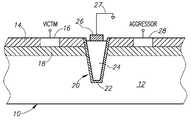
- FIG. 1A diagram illustrating an example a first embodiment deep trench capacitor noise isolation integrated device structure of the present invention is shown in FIG. 1 .
- the devicegenerally referenced 10 , comprises silicon substrate 12 , buried oxide (BOX) 18 , shallow trench isolation (STI) 14 , victim circuit devices 16 , aggressor circuit devices 28 and deep trench capacitor 20 .
- the deep trench capacitor 20comprises poly-silicon 24 , silicon dioxide layer 22 and CA metal contact 26 .
- the deep trench capacitoris electrically connected to ground node via connection 27 .
- the contact 26provides a good electrical connection between the deep trench capacitor and the ground node.
- the thickness of the silicon dioxide 22is not critical and is typically on the order of a few nanometers. It is desirable, however, to have as thin an oxide layer as possible to increase the effective capacitance coupling of the deep trench at low frequencies.
- the aggressor circuitmay comprise a processor or noisy input/output (IO) core.
- IOinput/output
- the switching operations of the circuit componentsWhen activated, the switching operations of the circuit components generate signals which couple through the capacitive coupling of the buried oxide (or through the diffusion capacitance in a bulk technology) into the substrate.
- the silicon substratewould couple the noise laterally to the area beneath the victim circuit, which may comprise, for example, a sensitive analog decision circuit such as an ADC.
- the noisewould further be coupled through the buried oxide to the victim circuit (e.g., sensitive device) and interfere with its operation.
- one or more deep trench capacitorsare used to shield the victim circuit from substrate noise.
- the deep trench capacitorsare connected through a low impedance 27 to ground and are operative to pull in the electric field lines from the aggressor circuit thereby “shading” the victim circuit from the substrate noise generated by the aggressor circuit devices.
- FIG. 2A schematic diagram illustrating the simplified equivalent circuit of the integrated device structure of FIG. 1 is shown in FIG. 2 .
- the circuitgenerally referenced 30 , comprises resistors 32 , 36 , 42 and capacitors 34 , 40 .
- the capacitors and resistorsrepresent the substrate losses, the deep trench capacitor edge capacitance and the series polysilicon resistance.
- the impedance 36is connected to ground which provides the relatively high shielding and noise isolation to the victim circuit.
- FIGS. 3A , 3 B, 3 C, 3 DDiagrams illustrating example steps for fabricating the deep trench capacitor of the present invention are shown in FIGS. 3A , 3 B, 3 C, 3 D.
- a flow diagram illustrating the method of fabricating the deep trench capacitor of the present inventionis shown in FIG. 4 .
- FIG. 3Aillustrates a device, generally referenced 50 , comprising substrate 56 , polysilicon 54 and silicon dioxide 52 .
- the device 50represents the starting point of the process, the fabrication of a conventional deep trench structure (step 140 ).
- FIG. 3Billustrates a device, generally referenced 60 , comprising substrate 68 , polysilicon 64 and silicon dioxide 62 .
- a contactis etched to the polysilicon by slightly over etching oxide when metal or polysilicon contacts are made to RX (step 142 ).
- Metal filled viasare used for connecting transistor drain, source and PC layer to the M1 metal layer.
- the RX layerdenotes the active area of various devices which is where the substrate doping is modified to form transistor drain and source regions, for example.
- FIG. 3Cillustrates a device, generally referenced 70 , comprising substrate 78 , polysilicon 74 and silicon dioxide 72 .
- the contactis fabricated with a silicon substrate (e.g., metal contact) in the area etched out in the previous step 142 (step 144 ).
- FIG. 3Dillustrates a device, generally referenced 80 , comprising substrate 89 , polysilicon 84 , silicon dioxide 82 and contact 86 .
- substrate 89polysilicon 84
- silicon dioxide 82silicon dioxide 82
- contact 86contact 86
- the ground connection 88provides the electrical shielding to prevent noise coupling from an aggressor circuit to a victim circuit located on the same substrate.
- the technique illustrated in FIG. 3is one example of constructing the DTCAP and that numerous other alternative well-known techniques may be used as well without departing from the scope of the invention.
- the DTCAPmay be constructed using a different polysilicon layer, silicon substrate contact, metal contact, etc.
- FIG. 5A diagram illustrating an second embodiment deep trench capacitor noise isolation integrated device structure of the present invention is shown in FIG. 5 .
- the devicegenerally referenced 90 , comprises substrate 99 , polysilicon 94 , silicon dioxide 93 , contact 96 , connection to ground 98 and halo implant 92 .
- Halo implantsare doped regions formed by bombarding the semiconductor wafer with tilted beams of ions, often used during the manufacture of semiconductor transistor devices.
- the halo implantsare formed by an anisotropic oxide etch which enables the halo implant at the bottom of the deep trench to contact the polysilicon fill 94 forming an ohmic contact between the polysilicon of the deep trench capacitor and the silicon substrate.
- FIG. 6A diagram illustrating an example of the second embodiment deep trench capacitor noise isolation integrated device structure of the present invention is shown in FIG. 6 .
- the devicegenerally referenced 100 , comprises silicon substrate 102 , buried oxide (BOX) 118 , shallow trench isolation (STI) 114 , victim circuit devices 116 , aggressor circuit devices 128 and deep trench capacitor 120 .
- the deep trench capacitor 120comprises poly-silicon 124 , silicon dioxide layer 122 and CA metal contact 126 .
- the deep trench capacitoris electrically connected to ground node via connection 127 .
- the contact 126provides a good electrical connection between the deep trench capacitor and the ground node.
- the second embodimentis essentially an extension of the deep trench device to a device which contacts the substrate at the bottom directly.
- This deviceis fabricated by (1) anisotropic oxide etch to clear the oxide at the bottom of the capacitor, (2) halo implant through the capacitor to dope the silicon below the capacitor; (3) fill of capacitor with poly; and (4) metal contact at the top of the capacitor poly.
- the halo implanthelps create a good contact between the poly (that fills the capacitor) and the now dopped silicon below the capacitor.
- FIG. 7A first diagram comparing the degree of isolation versus frequency for the deep trench capacitor of the present invention is shown in FIG. 7 .
- the resultscorrespond to a 10 micron spacing between the aggressor and the deep trench capacitor which itself is 6 microns deep, 1 micron wide with 0.5 micron poly silicon.
- Trace 132shows the isolation achieved by the first embodiment biased deep trench capacitor mechanism 10 ( FIG. 1 ).
- Trace 134shows the isolation achieved by the second embodiment grounded deep trench capacitor mechanism 100 ( FIG. 6 ).
- Trace 130shows the isolation achieved using unbiased (i.e. floating) deep trench devices. Note the almost 25 dB improvement in isolation of the second embodiment device over the first embodiment device. Note also the significant improvement in isolation for the first embodiment device at frequencies over 7-8 GHz.
- FIG. 8A diagram illustrating an example third embodiment deep trench capacitor noise isolation integrated device structure of the present invention fabricated in a triple well is shown in FIG. 8 .
- the device, generally referenced 150comprises p-type substrate 152 , n-well 166 , n+ regions 164 , p-well 168 , victim circuit and p+ region 172 , aggressor circuit and p+ region 174 , p-well 176 , deep trench capacitors 154 , polysilicon 158 , silicon dioxide 156 , contacts 160 and ground connections 162 .
- the deep trench capacitor isolation mechanism of FIGS. 1 and 6can be extended in bulk technologies to a triple well isolation mechanism with functions to further reduce noise coupling between aggressor and victim circuits.
- the addition of the n-doped bottom layer 166enables the victim circuit to be surrounded with a grounded ring from all directions which further increases the noise isolation by approximately an additional 10 dB at high frequencies compared to conventional triple well isolation.
- the victim circuitmay not necessarily be surrounded by the ground ring, as other configurations are also contemplated by the invention.
- the deep trench capacitordoes not necessarily completely enclose the victim circuit, as other configurations are also contemplated by the invention. For example different ground ring and deep trench capacitor configurations may be used depending on the particular circuit configuration implementation.
- the triple wellmay be replaced with a single or double well.
- FIG. 9A diagram illustrating an example a fourth embodiment deep trench capacitor noise isolation integrated device structure of the present invention fabricated in a triple well is shown in FIG. 9 .
- the devicegenerally referenced 180 , comprises p-type substrate 182 , n-well 228 , p-wells 222 , 226 , circuit # 1 220 , circuit # 2 224 , deep trench capacitors 184 , 186 , 188 , polysilicon 198 , 202 , 206 , silicon dioxide 196 , 200 , 204 , deep n-well contact points 190 , 192 , 194 , contacts 208 , 212 , 216 and ground connections 210 , 214 , 218 .
- this fourth embodiment of the deep trench capacitor isolation mechanismcan be used to make high density electrical contacts to a deep well rather than only contacts at the edges (i.e. perimeter) of the deep well since contacts will not effect p-wells or adjacent circuitry.
- the device 180may eliminate the use of implanted “plugs” for contacting deep wells.
- the device 180functions to anchor the deep well to a large capacitance.
- circuits # 1 and # 2represents any two circuits (i.e. digital or analog) that need isolation between them, i.e. aggressor and victim circuits, or two noisy circuits where noise from each circuit couples into the other circuit.
- FIG. 10A second diagram comparing the degree of isolation versus frequency for the deep trench capacitor of the present invention is shown in FIG. 10 .
- the resultscorrespond to a 10 micron spacing between the aggressor and the deep trench capacitor which itself is 6 microns deep, 1 micron wide with 0.5 micron poly silicon.
- Trace 136shows the isolation achieved by the first embodiment biased deep trench capacitor mechanism 10 ( FIG. 1 ).
- Trace 138shows the isolation achieved by the third embodiment (triple well) biased deep trench capacitor mechanism 150 ( FIG. 8 ). Note the improvement by over 30 dB in isolation of the triple well (third embodiment) device over the first embodiment device at low frequencies (e.g., less than 1 GHz). This improvement diminishes, however, as the frequency increases.
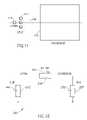
- FIG. 11A diagram illustrating a top down view of an example circuit is shown in FIG. 11 .
- the example circuitcomprises an aggressor circuit area 230 , deep trench capacitor structures of the present invention 232 and victim circuit area 234 . This is an example where the aggressor circuit is orders of magnitude larger than the victim circuit.
- FIG. 12A schematic diagram illustrating the equivalent circuit of the integrated device structure of FIG. 11 along the dotted horizontal line 236 is shown in FIG. 12 .
- the equivalent circuitgenerally referenced 240 , comprises a victim portion including parallel resistor 242 and capacitor 244 coupled to ground, an aggressor portion including parallel resistor 250 and capacitor 252 coupled to ground, and a mutual capacitance portion including parallel capacitor 246 and resistor 248 .
- Trace 260shows the mutual capacitance without the deep trench capacitor structure of the present invention.
- Trace 262shows the mutual capacitance with the deep trench capacitor structure of the present invention located 50 ⁇ m from the victim circuit area.
- Trace 264shows the mutual capacitance with the deep trench capacitor structure of the present invention located 10 ⁇ m from the victim circuit area. Note the significant drop in mutual capacitance (i.e. less noise coupling) with the deep trench capacitor at 10 ⁇ m especially at lower frequencies.
- the deep trench capacitor isolation mechanism of the present inventionincludes (1) the placement of substrate noise isolation ground contacts anywhere including within dense circuit designs without creating DC current paths or shorts between n and p wells; (2) relatively small additional complexity and cost to fabricate; (3) provides a grounded substrate contact placement under or to wells in a triple well process; (4) provides victim circuits relatively high noise isolation levels against neighboring aggressor circuits; (5) large sidewall capacitance maximizes the effective frequency operation range; and (6) triple and non-triple well deep trench device structures provide inherently large capacitance in guard rings that aid in providing ‘true’ ground potential at higher operating frequencies.
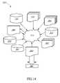
- FIG. 14A block diagram of an exemplary design flow of a design process used in semiconductor design, manufacturing, and/or testing of the deep trench capacitor of the present invention is shown in FIG. 14 .
- the design flowmay vary depending on the type of IC being designed. For example, a design flow for building an application specific IC (ASIC) may differ from a design flow for designing a standard component.
- Design structure 320is preferably an input to a design process 310 and may come from an IP provider, a core developer, or other design company or may be generated by the operator of the design flow, or from other sources.
- Design structure 320comprises an embodiment of the invention as shown in FIGS.
- Design structure 320may be contained on one or more machine readable medium.
- design structure 320may be a text file or a graphical representation of an embodiment of the invention as shown in FIGS. 1 , 3 A, 3 B, 3 C, 3 D, 5 , 6 , 8 and/or 9 .
- Design process 310preferably synthesizes (or translates) an embodiment of the invention as shown in FIGS.
- netlist 380is, for example, a list of wires, transistors, logic gates, control circuits, I/O, models, etc. that describes the connections to other elements and circuits in an integrated circuit design and recorded on at least one of machine readable medium. This may be an iterative process in which netlist 980 is re-synthesized one or more times depending on design specifications and parameters for the circuit.
- Design process 310may include using a variety of inputs; for example, inputs from library elements 330 which may house a set of commonly used elements, circuits, and devices, including models, layouts, and symbolic representations, for a given manufacturing technology (e.g., different technology nodes, 32 nm, 45 nm, 90 nm, etc.), design specifications 340 , characterization data 350 , verification data 360 , design rules 370 , and test data files 385 (which may include test patterns and other testing information).
- library elements 330which may house a set of commonly used elements, circuits, and devices, including models, layouts, and symbolic representations, for a given manufacturing technology (e.g., different technology nodes, 32 nm, 45 nm, 90 nm, etc.), design specifications 340 , characterization data 350 , verification data 360 , design rules 370 , and test data files 385 (which may include test patterns and other testing information).
- Design process 310may further include, for example, standard circuit design processes such as timing analysis, verification, design rule checking, place and route operations, etc.
- standard circuit design processessuch as timing analysis, verification, design rule checking, place and route operations, etc.
- Design process 310preferably translates an embodiment of the invention as shown in FIGS. 1 , 3 A, 3 B, 3 C, 3 D, 5 , 6 , 8 and/or 9 , along with any additional integrated circuit design or data (if applicable), into a second design structure 390 .
- Design structure 390resides on a storage medium in a data format used for the exchange of layout data of integrated circuits (e.g. information stored in a GDSII (GDS2), GL1, OASIS, or any other suitable format for storing such design structures).
- GDSIIGDS2
- GL1GL1, OASIS
- Design structure 390may comprise information such as, for example, test data files, design content files, manufacturing data, layout parameters, wires, levels of metal, vias, shapes, data for routing through the manufacturing line, and any other data required by a semiconductor manufacturer to produce an embodiment of the invention as shown in FIGS. 1 , 3 A, 3 B, 3 C, 3 D, 5 , 6 , 8 and/or 9 .
- Design structure 390may then proceed to a stage 395 where, for example, design structure 390 : proceeds to tape-out, is released to manufacturing, is released to a mask house, is sent to another design house, is sent back to the customer, etc.
Landscapes
- Engineering & Computer Science (AREA)
- Physics & Mathematics (AREA)
- Condensed Matter Physics & Semiconductors (AREA)
- General Physics & Mathematics (AREA)
- Manufacturing & Machinery (AREA)
- Computer Hardware Design (AREA)
- Microelectronics & Electronic Packaging (AREA)
- Power Engineering (AREA)
- Semiconductor Integrated Circuits (AREA)
Abstract
Description
- The present invention relates to the field of semiconductor manufacturing, and more particularly relates to bias-controlled deep trench substrate noise isolation integrated circuit device structures.
- The present invention is a novel and useful apparatus for and method of providing noise isolation between integrated circuit devices on a semiconductor chip. The invention addresses the problem of noise generated by digital switching devices in an integrated circuit chip that may couple through the silicon substrate into sensitive analog circuits (e.g., PLLs, transceivers, ADCs, etc.) causing a significant degradation in performance of the sensitive analog circuits. The invention utilizes a deep trench capacitor (DTCAP) device connected to ground to isolate victim circuits from aggressor noise sources on the same integrated circuit chip. The deep penetration of the capacitor creates a grounded shield deep in the substrate as compared with other prior art shielding techniques.
- There is thus provided in accordance with the present invention, an integrated circuit device, comprising a semiconductor substrate having a first portion in which aggressor devices are formed and a second portion in which victim devices are formed, a deep trench capacitor having a first node and a second node, said deep trench capacitor formed between said first portion and said second portion, and wherein said first node of said deep trench capacitor is electrically connected to a ground node.
- There is also provided in accordance with the present invention, a design structure embodied in a machine readable medium for designing, manufacturing, or testing an integrated circuit, the design structure comprising a semiconductor substrate having a first portion in which aggressor devices are formed and a second portion in which victim devices are formed, a deep trench capacitor formed between said first portion and said second portion, and wherein said deep trench capacitor is electrically connected to a ground node.
- There is further provided in accordance with the present invention, an integrated circuit device, comprising a semiconductor substrate having a first portion in which one or more aggressor devices are formed, a well portion formed in said semiconductor substrate, and said well comprising one or more victim devices and a deep trench capacitor operative to electrically couple said well portion to a ground node.
- There is also provided in accordance with the present invention, a method of noise isolation for use in an integrated circuit device, the method comprising the steps of providing a semiconductor substrate having a first portion in which aggressor devices are formed and a second portion in which victim devices are formed, forming a deep trench capacitor between said first portion and said second portion, and electrically connecting said deep trench capacitor to a ground node.
- The invention is herein described, by way of example only, with reference to the accompanying drawings, wherein:
FIG. 1 is a diagram illustrating an example a first embodiment deep trench capacitor noise isolation integrated device structure of the present invention;FIG. 2 is a schematic diagram illustrating the equivalent circuit of the integrated device structure ofFIG. 1 ;FIGS. 3A ,3B,3C,3D are diagrams illustrating example steps for fabricating the deep trench capacitor of the present invention;FIG. 4 is a flow diagram illustrating the method of fabricating the deep trench capacitor of the present invention;FIG. 5 is a diagram illustrating an example second embodiment deep trench capacitor noise isolation integrated device structure of the present invention;FIG. 6 is a diagram illustrating a second example of the second embodiment deep trench capacitor noise isolation integrated device structure of the present invention;FIG. 7 is a first diagram comparing the degree of isolation versus frequency for the deep trench capacitor of the present invention;FIG. 8 is a diagram illustrating an example third embodiment deep trench capacitor noise isolation integrated device structure of the present invention fabricated in a triple well;FIG. 9 is a diagram illustrating an example a fourth embodiment deep trench capacitor noise isolation integrated device structure of the present invention fabricated in a triple well;FIG. 10 is a second diagram comparing the degree of isolation versus frequency for the deep trench capacitor of the present invention;FIG. 11 is a diagram illustrating a top down view of an example circuit;FIG. 12 is a schematic diagram illustrating the equivalent circuit of the integrated device structure ofFIG. 11 along the dotted horizontal line;FIG. 13 is a diagram illustrating the behavior of the coupling capacitance value; andFIG. 14 is a block diagram of an exemplary design flow of a design process used in semiconductor design, manufacturing, and/or testing of the deep trench capacitor of the present invention.- The following notation is used throughout this document:
Term Definition ADC Analog to Digital Converter ASIC Application Specific Integrated Circuit BOX Bulk Oxide CMOS Complementary Metal Oxide Semiconductor DC Direct Current DTCAP Deep Trench Capacitor HDL Hardware Description Language IC Integrated Circuit IO Input/Output IP Intellectual Property PLL Phase Locked Loop SOI Silicon On Insulator STI Shallow Trench Isolation VHDL Very High Density Lithography - The present invention is an apparatus for and method of providing noise isolation between integrated circuit devices on a semiconductor chip. The invention addresses the problem of noise generated by digital switching devices in an integrated circuit chip. The noise may couple through the silicon substrate into sensitive analog circuits (e.g., PLLs, transceivers, ADCs, etc.) causing a significant degradation in performance of the sensitive analog circuits.
- For example, in processor based integrated circuit chips, the processor circuit portion is the dominant noise source compared to neighboring analog circuits such as ADCs, due to the high switching activity of the digital logic devices of the processor. The effective noise generating area of the processor can be expressed as a function of the active area and activity factor of the switching devices, as shown below in
Equation 1.
Aeffective=C×F×Atotal (1)- where
- Aeffectiveis the effective noise-generating area of the processor;
- Atotalis the total processor area;
- C is the percentage of the active (i.e. transistor) area of the processor;
- F is the activity factor (i.e. percentage of devices switching in phase);
- The invention utilizes a deep trench capacitor (DTCAP) device connected to ground to isolate victim circuits from aggressor noise sources on the same integrated circuit chip. Note that the aggressor and victim circuit may comprise analog, digital, or any combination of analog and digital circuits.
- Note that references to ground include both AC and DC ground, where AC ground is a ground for any frequency above DC. In addition, depending on the implementation, a connection to ground may include a connection to a power supply such as VDD.
- In operation, the deep trench capacitor is placed between the aggressor and victim circuit portions of the integrated circuit. The deep trench capacitor is available in most semiconductor technologies and requires relatively very little chip real estate area and penetrates deep into the substrate (e.g., 4-6 μm). The deep penetration of the capacitor creates a grounded shield deep in the substrate as compared with other prior art shielding techniques.
- The improved isolation of the deep trench capacitor extends to relatively high frequencies and is not limited to the lower frequency range (as is the case with prior art floating deep trench isolation). In application, the deep trench capacitor isolation mechanism of the present invention can be used in conjunction with additional isolation techniques to increase the overall isolation.
- A diagram illustrating an example a first embodiment deep trench capacitor noise isolation integrated device structure of the present invention is shown in
FIG. 1 . The device, generally referenced10, comprisessilicon substrate 12, buried oxide (BOX)18, shallow trench isolation (STI)14,victim circuit devices 16,aggressor circuit devices 28 anddeep trench capacitor 20. Thedeep trench capacitor 20 comprises poly-silicon 24,silicon dioxide layer 22 andCA metal contact 26. - In accordance with the invention, the deep trench capacitor is electrically connected to ground node via
connection 27. Thecontact 26 provides a good electrical connection between the deep trench capacitor and the ground node. Note that the thickness of thesilicon dioxide 22 is not critical and is typically on the order of a few nanometers. It is desirable, however, to have as thin an oxide layer as possible to increase the effective capacitance coupling of the deep trench at low frequencies. - Note that the example deep trench capacitor isolation mechanism presented herein is for silicon on insulator (SOI) technology which has inherent substrate noise isolation compared to bulk technology. It is appreciated that one skilled in the semiconductor arts can apply the principles of the present invention to implementations in standard CMOS bulk technologies.
- The aggressor circuit may comprise a processor or noisy input/output (IO) core. When activated, the switching operations of the circuit components generate signals which couple through the capacitive coupling of the buried oxide (or through the diffusion capacitance in a bulk technology) into the substrate. Without the benefit of the present invention, the silicon substrate would couple the noise laterally to the area beneath the victim circuit, which may comprise, for example, a sensitive analog decision circuit such as an ADC. The noise would further be coupled through the buried oxide to the victim circuit (e.g., sensitive device) and interfere with its operation.
- In accordance with the present invention, one or more deep trench capacitors are used to shield the victim circuit from substrate noise. The deep trench capacitors are connected through a
low impedance 27 to ground and are operative to pull in the electric field lines from the aggressor circuit thereby “shading” the victim circuit from the substrate noise generated by the aggressor circuit devices. - A schematic diagram illustrating the simplified equivalent circuit of the integrated device structure of
FIG. 1 is shown inFIG. 2 . The circuit, generally referenced30, comprisesresistors capacitors impedance 36 is connected to ground which provides the relatively high shielding and noise isolation to the victim circuit. - Significant isolation is achieved even with a relatively small separation between the aggressor and victim circuits. For example, with 100 μm between aggressor and victim circuits, a coupling as low as −57 dB at a frequency of 2 GHz can be achieved.
- Diagrams illustrating example steps for fabricating the deep trench capacitor of the present invention are shown in
FIGS. 3A ,3B,3C,3D. A flow diagram illustrating the method of fabricating the deep trench capacitor of the present invention is shown inFIG. 4 . FIG. 3A illustrates a device, generally referenced50, comprisingsubstrate 56,polysilicon 54 andsilicon dioxide 52. Thedevice 50 represents the starting point of the process, the fabrication of a conventional deep trench structure (step140).FIG. 3B illustrates a device, generally referenced60, comprisingsubstrate 68,polysilicon 64 andsilicon dioxide 62. After fabrication of a conventional deep trench structure, a contact is etched to the polysilicon by slightly over etching oxide when metal or polysilicon contacts are made to RX (step142). Metal filled vias are used for connecting transistor drain, source and PC layer to the M1 metal layer. The RX layer denotes the active area of various devices which is where the substrate doping is modified to form transistor drain and source regions, for example.FIG. 3C illustrates a device, generally referenced70, comprisingsubstrate 78,polysilicon 74 andsilicon dioxide 72. In this step, the contact is fabricated with a silicon substrate (e.g., metal contact) in the area etched out in the previous step142 (step144).FIG. 3D illustrates a device, generally referenced80, comprisingsubstrate 89,polysilicon 84,silicon dioxide 82 andcontact 86. To achieve noise isolation, after the deep trench capacitor is fabricated with the contact, it is electrically connected to a ground node (step146). Theground connection 88 provides the electrical shielding to prevent noise coupling from an aggressor circuit to a victim circuit located on the same substrate.- Note that there may be variations in the construction of the deep trench capacitor. It is appreciated that the technique illustrated in
FIG. 3 is one example of constructing the DTCAP and that numerous other alternative well-known techniques may be used as well without departing from the scope of the invention. For example, the DTCAP may be constructed using a different polysilicon layer, silicon substrate contact, metal contact, etc. - A diagram illustrating an second embodiment deep trench capacitor noise isolation integrated device structure of the present invention is shown in
FIG. 5 . The device, generally referenced90, comprisessubstrate 99,polysilicon 94,silicon dioxide 93,contact 96, connection to ground98 andhalo implant 92. Halo implants, well known in the art, are doped regions formed by bombarding the semiconductor wafer with tilted beams of ions, often used during the manufacture of semiconductor transistor devices. The halo implants are formed by an anisotropic oxide etch which enables the halo implant at the bottom of the deep trench to contact the polysilicon fill94 forming an ohmic contact between the polysilicon of the deep trench capacitor and the silicon substrate. - A diagram illustrating an example of the second embodiment deep trench capacitor noise isolation integrated device structure of the present invention is shown in
FIG. 6 . The device, generally referenced100, comprisessilicon substrate 102, buried oxide (BOX)118, shallow trench isolation (STI)114,victim circuit devices 116, aggressor circuit devices128 anddeep trench capacitor 120. Thedeep trench capacitor 120 comprises poly-silicon 124,silicon dioxide layer 122 andCA metal contact 126. In accordance with the invention, the deep trench capacitor is electrically connected to ground node viaconnection 127. Thecontact 126 provides a good electrical connection between the deep trench capacitor and the ground node. - In this second embodiment, there is no bottom layer of oxide under the
deep trench 120. This results in better isolation over a broad frequency range. The improvement in isolation is due to the non dielectric bottom contact which results in a good connection even for very low frequencies (in principle down to DC). - Note that the second embodiment is essentially an extension of the deep trench device to a device which contacts the substrate at the bottom directly. This device is fabricated by (1) anisotropic oxide etch to clear the oxide at the bottom of the capacitor, (2) halo implant through the capacitor to dope the silicon below the capacitor; (3) fill of capacitor with poly; and (4) metal contact at the top of the capacitor poly. The halo implant helps create a good contact between the poly (that fills the capacitor) and the now dopped silicon below the capacitor.
- A first diagram comparing the degree of isolation versus frequency for the deep trench capacitor of the present invention is shown in
FIG. 7 . The results correspond to a 10 micron spacing between the aggressor and the deep trench capacitor which itself is 6 microns deep, 1 micron wide with 0.5 micron poly silicon.Trace 132 shows the isolation achieved by the first embodiment biased deep trench capacitor mechanism10 (FIG. 1 ).Trace 134 shows the isolation achieved by the second embodiment grounded deep trench capacitor mechanism100 (FIG. 6 ).Trace 130 shows the isolation achieved using unbiased (i.e. floating) deep trench devices. Note the almost 25 dB improvement in isolation of the second embodiment device over the first embodiment device. Note also the significant improvement in isolation for the first embodiment device at frequencies over 7-8 GHz. - A diagram illustrating an example third embodiment deep trench capacitor noise isolation integrated device structure of the present invention fabricated in a triple well is shown in
FIG. 8 . The device, generally referenced150, comprises p-type substrate 152, n-well166,n+ regions 164, p-well168, victim circuit andp+ region 172, aggressor circuit andp+ region 174, p-well176,deep trench capacitors 154,polysilicon 158,silicon dioxide 156,contacts 160 andground connections 162. - The deep trench capacitor isolation mechanism of
FIGS. 1 and 6 can be extended in bulk technologies to a triple well isolation mechanism with functions to further reduce noise coupling between aggressor and victim circuits. The addition of the n-dopedbottom layer 166 enables the victim circuit to be surrounded with a grounded ring from all directions which further increases the noise isolation by approximately an additional 10 dB at high frequencies compared to conventional triple well isolation. Note that the victim circuit may not necessarily be surrounded by the ground ring, as other configurations are also contemplated by the invention. In addition, the deep trench capacitor does not necessarily completely enclose the victim circuit, as other configurations are also contemplated by the invention. For example different ground ring and deep trench capacitor configurations may be used depending on the particular circuit configuration implementation. In alternative embodiments, the triple well may be replaced with a single or double well. - A diagram illustrating an example a fourth embodiment deep trench capacitor noise isolation integrated device structure of the present invention fabricated in a triple well is shown in
FIG. 9 . The device, generally referenced180, comprises p-type substrate 182, n-well228, p-wells circuit # 1220,circuit # 2224,deep trench capacitors polysilicon silicon dioxide contacts ground connections - In triple well devices, this fourth embodiment of the deep trench capacitor isolation mechanism can be used to make high density electrical contacts to a deep well rather than only contacts at the edges (i.e. perimeter) of the deep well since contacts will not effect p-wells or adjacent circuitry. The
device 180 may eliminate the use of implanted “plugs” for contacting deep wells. In addition, thedevice 180 functions to anchor the deep well to a large capacitance. Note thatcircuits # 1 and #2 represents any two circuits (i.e. digital or analog) that need isolation between them, i.e. aggressor and victim circuits, or two noisy circuits where noise from each circuit couples into the other circuit. - A second diagram comparing the degree of isolation versus frequency for the deep trench capacitor of the present invention is shown in
FIG. 10 . The results correspond to a 10 micron spacing between the aggressor and the deep trench capacitor which itself is 6 microns deep, 1 micron wide with 0.5 micron poly silicon.Trace 136 shows the isolation achieved by the first embodiment biased deep trench capacitor mechanism10 (FIG. 1 ).Trace 138 shows the isolation achieved by the third embodiment (triple well) biased deep trench capacitor mechanism150 (FIG. 8 ). Note the improvement by over 30 dB in isolation of the triple well (third embodiment) device over the first embodiment device at low frequencies (e.g., less than 1 GHz). This improvement diminishes, however, as the frequency increases. - A diagram illustrating a top down view of an example circuit is shown in
FIG. 11 . The example circuit comprises anaggressor circuit area 230, deep trench capacitor structures of thepresent invention 232 andvictim circuit area 234. This is an example where the aggressor circuit is orders of magnitude larger than the victim circuit. - A schematic diagram illustrating the equivalent circuit of the integrated device structure of
FIG. 11 along the dottedhorizontal line 236 is shown inFIG. 12 . The equivalent circuit, generally referenced240, comprises a victim portion includingparallel resistor 242 andcapacitor 244 coupled to ground, an aggressor portion includingparallel resistor 250 andcapacitor 252 coupled to ground, and a mutual capacitance portion includingparallel capacitor 246 andresistor 248. - A diagram illustrating the behavior of the coupling capacitance value of the scenario shown in
FIG. 11 is shown inFIG. 13 .Trace 260 shows the mutual capacitance without the deep trench capacitor structure of the present invention.Trace 262 shows the mutual capacitance with the deep trench capacitor structure of the present invention located 50 μm from the victim circuit area.Trace 264 shows the mutual capacitance with the deep trench capacitor structure of the present invention located 10 μm from the victim circuit area. Note the significant drop in mutual capacitance (i.e. less noise coupling) with the deep trench capacitor at 10 μm especially at lower frequencies. - Several advantages of the deep trench capacitor isolation mechanism of the present invention include (1) the placement of substrate noise isolation ground contacts anywhere including within dense circuit designs without creating DC current paths or shorts between n and p wells; (2) relatively small additional complexity and cost to fabricate; (3) provides a grounded substrate contact placement under or to wells in a triple well process; (4) provides victim circuits relatively high noise isolation levels against neighboring aggressor circuits; (5) large sidewall capacitance maximizes the effective frequency operation range; and (6) triple and non-triple well deep trench device structures provide inherently large capacitance in guard rings that aid in providing ‘true’ ground potential at higher operating frequencies.
- A block diagram of an exemplary design flow of a design process used in semiconductor design, manufacturing, and/or testing of the deep trench capacitor of the present invention is shown in
FIG. 14 . The design flow, generally referenced300, may vary depending on the type of IC being designed. For example, a design flow for building an application specific IC (ASIC) may differ from a design flow for designing a standard component.Design structure 320 is preferably an input to adesign process 310 and may come from an IP provider, a core developer, or other design company or may be generated by the operator of the design flow, or from other sources.Design structure 320 comprises an embodiment of the invention as shown inFIGS. 1 ,3A,3B,3C,3D,5,6,8 and/or9 in the form of schematics or HDL, a hardware-description language (e.g., Verilog, VHDL, C, etc.).Design structure 320 may be contained on one or more machine readable medium. For example,design structure 320 may be a text file or a graphical representation of an embodiment of the invention as shown inFIGS. 1 ,3A,3B,3C,3D,5,6,8 and/or9.Design process 310 preferably synthesizes (or translates) an embodiment of the invention as shown inFIGS. 1 ,3A,3B,3C,3D,5,6,8 and/or9 into anetlist 380, wherenetlist 380 is, for example, a list of wires, transistors, logic gates, control circuits, I/O, models, etc. that describes the connections to other elements and circuits in an integrated circuit design and recorded on at least one of machine readable medium. This may be an iterative process in which netlist980 is re-synthesized one or more times depending on design specifications and parameters for the circuit. Design process 310 may include using a variety of inputs; for example, inputs fromlibrary elements 330 which may house a set of commonly used elements, circuits, and devices, including models, layouts, and symbolic representations, for a given manufacturing technology (e.g., different technology nodes, 32 nm, 45 nm, 90 nm, etc.),design specifications 340,characterization data 350,verification data 360,design rules 370, and test data files385 (which may include test patterns and other testing information).Design process 310 may further include, for example, standard circuit design processes such as timing analysis, verification, design rule checking, place and route operations, etc. One of ordinary skill in the art of integrated circuit design can appreciate the extent of possible electronic design automation tools and applications used indesign process 310 without deviating from the scope and spirit of the invention. The design structure of the invention is not limited to any specific design flow.Design process 310 preferably translates an embodiment of the invention as shown inFIGS. 1 ,3A,3B,3C,3D,5,6,8 and/or9, along with any additional integrated circuit design or data (if applicable), into asecond design structure 390.Design structure 390 resides on a storage medium in a data format used for the exchange of layout data of integrated circuits (e.g. information stored in a GDSII (GDS2), GL1, OASIS, or any other suitable format for storing such design structures).Design structure 390 may comprise information such as, for example, test data files, design content files, manufacturing data, layout parameters, wires, levels of metal, vias, shapes, data for routing through the manufacturing line, and any other data required by a semiconductor manufacturer to produce an embodiment of the invention as shown inFIGS. 1 ,3A,3B,3C,3D,5,6,8 and/or9.Design structure 390 may then proceed to astage 395 where, for example, design structure390: proceeds to tape-out, is released to manufacturing, is released to a mask house, is sent to another design house, is sent back to the customer, etc.- The terminology used herein is for the purpose of describing particular embodiments only and is not intended to be limiting of the invention. As used herein, the singular forms “a”, “an” and “the” are intended to include the plural forms as well, unless the context clearly indicates otherwise. It will be further understood that the terms “comprises” and/or “comprising,” when used in this specification, specify the presence of stated features, integers, steps, operations, elements, and/or components, but do not preclude the presence or addition of one or more other features, integers, steps, operations, elements, components, and/or groups thereof.
- The corresponding structures, materials, acts, and equivalents of all means or step plus function elements in the claims below are intended to include any structure, material, or act for performing the function in combination with other claimed elements as specifically claimed. The description of the present invention has been presented for purposes of illustration and description, but is not intended to be exhaustive or limited to the invention in the form disclosed. As numerous modifications and changes will readily occur to those skilled in the art, it is intended that the invention not be limited to the limited number of embodiments described herein. Accordingly, it will be appreciated that all suitable variations, modifications and equivalents may be resorted to, falling within the spirit and scope of the present invention. The embodiments were chosen and described in order to best explain the principles of the invention and the practical application, and to enable others of ordinary skill in the art to understand the invention for various embodiments with various modifications as are suited to the particular use contemplated.
Claims (18)
Priority Applications (2)
| Application Number | Priority Date | Filing Date | Title |
|---|---|---|---|
| US12/506,270US8021941B2 (en) | 2009-07-21 | 2009-07-21 | Bias-controlled deep trench substrate noise isolation integrated circuit device structures |
| US13/207,480US8212332B2 (en) | 2009-07-21 | 2011-08-11 | Bias-controlled deep trench substrate noise isolation integrated circuit device structures |
Applications Claiming Priority (1)
| Application Number | Priority Date | Filing Date | Title |
|---|---|---|---|
| US12/506,270US8021941B2 (en) | 2009-07-21 | 2009-07-21 | Bias-controlled deep trench substrate noise isolation integrated circuit device structures |
Related Child Applications (1)
| Application Number | Title | Priority Date | Filing Date |
|---|---|---|---|
| US13/207,480ContinuationUS8212332B2 (en) | 2009-07-21 | 2011-08-11 | Bias-controlled deep trench substrate noise isolation integrated circuit device structures |
Publications (2)
| Publication Number | Publication Date |
|---|---|
| US20110018094A1true US20110018094A1 (en) | 2011-01-27 |
| US8021941B2 US8021941B2 (en) | 2011-09-20 |
Family
ID=43496534
Family Applications (2)
| Application Number | Title | Priority Date | Filing Date |
|---|---|---|---|
| US12/506,270Active2029-12-29US8021941B2 (en) | 2009-07-21 | 2009-07-21 | Bias-controlled deep trench substrate noise isolation integrated circuit device structures |
| US13/207,480ActiveUS8212332B2 (en) | 2009-07-21 | 2011-08-11 | Bias-controlled deep trench substrate noise isolation integrated circuit device structures |
Family Applications After (1)
| Application Number | Title | Priority Date | Filing Date |
|---|---|---|---|
| US13/207,480ActiveUS8212332B2 (en) | 2009-07-21 | 2011-08-11 | Bias-controlled deep trench substrate noise isolation integrated circuit device structures |
Country Status (1)
| Country | Link |
|---|---|
| US (2) | US8021941B2 (en) |
Cited By (20)
| Publication number | Priority date | Publication date | Assignee | Title |
|---|---|---|---|---|
| US20110062542A1 (en)* | 2009-09-17 | 2011-03-17 | International Business Machines Corporation | Structures, design structures and methods of fabricating global shutter pixel sensor cells |
| CN102751230A (en)* | 2011-04-21 | 2012-10-24 | 飞思卡尔半导体公司 | Isolated capacitors within shallow trench isolation |
| US8456187B2 (en) | 2011-04-21 | 2013-06-04 | International Business Machines Corporation | Implementing temporary disable function of protected circuitry by modulating threshold voltage of timing sensitive circuit |
| US8492207B2 (en) | 2011-04-21 | 2013-07-23 | International Business Machines Corporation | Implementing eFuse circuit with enhanced eFuse blow operation |
| US8525245B2 (en) | 2011-04-21 | 2013-09-03 | International Business Machines Corporation | eDRAM having dynamic retention and performance tradeoff |
| US8816470B2 (en) | 2011-04-21 | 2014-08-26 | International Business Machines Corporation | Independently voltage controlled volume of silicon on a silicon on insulator chip |
| CN104867864A (en)* | 2015-03-27 | 2015-08-26 | 上海新储集成电路有限公司 | Method for realizing local interconnection |
| FR3057393A1 (en)* | 2016-10-11 | 2018-04-13 | Stmicroelectronics (Rousset) Sas | INTEGRATED CIRCUIT WITH DECOUPLING CAPACITOR IN A TYPE TRIPLE CAISSON STRUCTURE |
| US10229928B2 (en) | 2012-06-27 | 2019-03-12 | Intel Corporation | Three dimensional NAND flash with self-aligned select gate |
| US10319678B2 (en) | 2014-09-26 | 2019-06-11 | Intel Corporation | Capping poly channel pillars in stacked circuits |
| US10818669B2 (en) | 2017-08-28 | 2020-10-27 | Stmicroelectronics (Rousset) Sas | Integrated circuit with vertically structured capacitive element, and its fabricating process |
| US10879233B2 (en) | 2017-08-28 | 2020-12-29 | Stmicroelectronics (Rousset) Sas | Process for fabricating capacitive elements in trenches |
| US10943862B2 (en) | 2018-01-09 | 2021-03-09 | Stmicroelectronics (Rousset) Sas | Integrated filler capacitor cell device and corresponding manufacturing method |
| US10969376B2 (en)* | 2016-09-19 | 2021-04-06 | Murata Integrated Passive Solutions | Electrical stimulation and monitoring device |
| US10971578B2 (en) | 2018-10-08 | 2021-04-06 | Stmicroelectronics (Rousset) Sas | Capacitive electronic chip component |
| US20210118772A1 (en)* | 2019-10-18 | 2021-04-22 | Taiwan Semiconductor Manufacturing Company Limited | Semiconductor arrangement and method for making |
| US11004785B2 (en) | 2019-08-21 | 2021-05-11 | Stmicroelectronics (Rousset) Sas | Co-integrated vertically structured capacitive element and fabrication process |
| US11018149B2 (en) | 2014-03-27 | 2021-05-25 | Intel Corporation | Building stacked hollow channels for a three dimensional circuit device |
| US11183452B1 (en) | 2020-08-12 | 2021-11-23 | Infineon Technologies Austria Ag | Transfering informations across a high voltage gap using capacitive coupling with DTI integrated in silicon technology |
| US11621222B2 (en) | 2018-01-09 | 2023-04-04 | Stmicroelectronics (Rousset) Sas | Integrated filler capacitor cell device and corresponding manufacturing method |
Families Citing this family (4)
| Publication number | Priority date | Publication date | Assignee | Title |
|---|---|---|---|---|
| US20110115047A1 (en)* | 2009-11-13 | 2011-05-19 | Francois Hebert | Semiconductor process using mask openings of varying widths to form two or more device structures |
| KR20120092878A (en)* | 2011-02-14 | 2012-08-22 | 에스케이하이닉스 주식회사 | Semiconductor device and method for fabricating the same |
| US8927989B2 (en) | 2012-11-28 | 2015-01-06 | International Business Machines Corporation | Voltage contrast inspection of deep trench isolation |
| CN114188311A (en) | 2020-09-15 | 2022-03-15 | 联华电子股份有限公司 | Semiconductor structure |
Citations (6)
| Publication number | Priority date | Publication date | Assignee | Title |
|---|---|---|---|---|
| US6121148A (en)* | 1998-02-17 | 2000-09-19 | National Semiconductor Corporation | Semiconductor device trench isolation structure with polysilicon bias voltage contact |
| US6396121B1 (en)* | 2000-05-31 | 2002-05-28 | International Business Machines Corporation | Structures and methods of anti-fuse formation in SOI |
| US6498372B2 (en)* | 2001-02-16 | 2002-12-24 | International Business Machines Corporation | Conductive coupling of electrical structures to a semiconductor device located under a buried oxide layer |
| US6544837B1 (en)* | 2000-03-17 | 2003-04-08 | International Business Machines Corporation | SOI stacked DRAM logic |
| US20070145489A1 (en)* | 2005-12-27 | 2007-06-28 | Taiwan Semiconductor Manufacturing Company, Ltd. | Design of high-frequency substrate noise isolation in BiCMOS technology |
| US20080073747A1 (en)* | 2006-09-22 | 2008-03-27 | Clinton Chao | Electromagnetic shielding using through-silicon vias |
Family Cites Families (5)
| Publication number | Priority date | Publication date | Assignee | Title |
|---|---|---|---|---|
| JP2006049413A (en)* | 2004-08-02 | 2006-02-16 | Fujitsu Ltd | Semiconductor device and manufacturing method thereof |
| US7022565B1 (en)* | 2004-11-26 | 2006-04-04 | Grace Semiconductor Manufacturing Corporation | Method of fabricating a trench capacitor of a mixed mode integrated circuit |
| JP2006310576A (en)* | 2005-04-28 | 2006-11-09 | Renesas Technology Corp | Semiconductor device and manufacturing method thereof |
| KR100833180B1 (en)* | 2006-07-06 | 2008-05-28 | 삼성전자주식회사 | Semiconductor device having STI structure and its manufacturing method |
| DE102008007002B4 (en)* | 2008-01-31 | 2013-03-28 | Advanced Micro Devices, Inc. | A method of forming substrate contacts for advanced SOI devices based on a deep trench capacitor configuration |
- 2009
- 2009-07-21USUS12/506,270patent/US8021941B2/enactiveActive
- 2011
- 2011-08-11USUS13/207,480patent/US8212332B2/enactiveActive
Patent Citations (6)
| Publication number | Priority date | Publication date | Assignee | Title |
|---|---|---|---|---|
| US6121148A (en)* | 1998-02-17 | 2000-09-19 | National Semiconductor Corporation | Semiconductor device trench isolation structure with polysilicon bias voltage contact |
| US6544837B1 (en)* | 2000-03-17 | 2003-04-08 | International Business Machines Corporation | SOI stacked DRAM logic |
| US6396121B1 (en)* | 2000-05-31 | 2002-05-28 | International Business Machines Corporation | Structures and methods of anti-fuse formation in SOI |
| US6498372B2 (en)* | 2001-02-16 | 2002-12-24 | International Business Machines Corporation | Conductive coupling of electrical structures to a semiconductor device located under a buried oxide layer |
| US20070145489A1 (en)* | 2005-12-27 | 2007-06-28 | Taiwan Semiconductor Manufacturing Company, Ltd. | Design of high-frequency substrate noise isolation in BiCMOS technology |
| US20080073747A1 (en)* | 2006-09-22 | 2008-03-27 | Clinton Chao | Electromagnetic shielding using through-silicon vias |
Cited By (36)
| Publication number | Priority date | Publication date | Assignee | Title |
|---|---|---|---|---|
| US20110062542A1 (en)* | 2009-09-17 | 2011-03-17 | International Business Machines Corporation | Structures, design structures and methods of fabricating global shutter pixel sensor cells |
| US8138531B2 (en)* | 2009-09-17 | 2012-03-20 | International Business Machines Corporation | Structures, design structures and methods of fabricating global shutter pixel sensor cells |
| US8456187B2 (en) | 2011-04-21 | 2013-06-04 | International Business Machines Corporation | Implementing temporary disable function of protected circuitry by modulating threshold voltage of timing sensitive circuit |
| US8492207B2 (en) | 2011-04-21 | 2013-07-23 | International Business Machines Corporation | Implementing eFuse circuit with enhanced eFuse blow operation |
| US8525245B2 (en) | 2011-04-21 | 2013-09-03 | International Business Machines Corporation | eDRAM having dynamic retention and performance tradeoff |
| US8816470B2 (en) | 2011-04-21 | 2014-08-26 | International Business Machines Corporation | Independently voltage controlled volume of silicon on a silicon on insulator chip |
| TWI549166B (en)* | 2011-04-21 | 2016-09-11 | 飛思卡爾半導體公司 | Isolation capacitor in shallow trench isolation |
| CN102751230A (en)* | 2011-04-21 | 2012-10-24 | 飞思卡尔半导体公司 | Isolated capacitors within shallow trench isolation |
| US10229928B2 (en) | 2012-06-27 | 2019-03-12 | Intel Corporation | Three dimensional NAND flash with self-aligned select gate |
| US11018149B2 (en) | 2014-03-27 | 2021-05-25 | Intel Corporation | Building stacked hollow channels for a three dimensional circuit device |
| US10319678B2 (en) | 2014-09-26 | 2019-06-11 | Intel Corporation | Capping poly channel pillars in stacked circuits |
| CN104867864A (en)* | 2015-03-27 | 2015-08-26 | 上海新储集成电路有限公司 | Method for realizing local interconnection |
| US10969376B2 (en)* | 2016-09-19 | 2021-04-06 | Murata Integrated Passive Solutions | Electrical stimulation and monitoring device |
| FR3057393A1 (en)* | 2016-10-11 | 2018-04-13 | Stmicroelectronics (Rousset) Sas | INTEGRATED CIRCUIT WITH DECOUPLING CAPACITOR IN A TYPE TRIPLE CAISSON STRUCTURE |
| US10535672B2 (en) | 2016-10-11 | 2020-01-14 | Stmicroelectronics (Rousset) Sas | Integrated circuit with decoupling capacitor in a structure of the triple well type |
| US10651184B2 (en) | 2016-10-11 | 2020-05-12 | Stmicroelectronics (Rousset) Sas | Integrated circuit with decoupling capacitor in a structure of the triple well type |
| CN107919360A (en)* | 2016-10-11 | 2018-04-17 | 意法半导体(鲁塞)公司 | Using the integrated circuit with decoupling capacitor of three well-type structures |
| US10818669B2 (en) | 2017-08-28 | 2020-10-27 | Stmicroelectronics (Rousset) Sas | Integrated circuit with vertically structured capacitive element, and its fabricating process |
| US10879233B2 (en) | 2017-08-28 | 2020-12-29 | Stmicroelectronics (Rousset) Sas | Process for fabricating capacitive elements in trenches |
| US11081488B2 (en) | 2017-08-28 | 2021-08-03 | Stmicroelectronics (Rousset) Sas | Integrated circuit with vertically structured capacitive element, and its fabricating process |
| US11139303B2 (en) | 2017-08-28 | 2021-10-05 | Stmicroelectronics (Rousset) Sas | Integrated circuit with vertically structured capacitive element, and its fabricating process |
| US11621222B2 (en) | 2018-01-09 | 2023-04-04 | Stmicroelectronics (Rousset) Sas | Integrated filler capacitor cell device and corresponding manufacturing method |
| US10943862B2 (en) | 2018-01-09 | 2021-03-09 | Stmicroelectronics (Rousset) Sas | Integrated filler capacitor cell device and corresponding manufacturing method |
| US12230565B2 (en) | 2018-01-09 | 2025-02-18 | Stmicroelectronics (Rousset) Sas | Integrated filler capacitor cell device and corresponding manufacturing method |
| US11935828B2 (en) | 2018-01-09 | 2024-03-19 | Stmicroelectronics (Rousset) Sas | Integrated filler capacitor cell device and corresponding manufacturing method |
| US10971578B2 (en) | 2018-10-08 | 2021-04-06 | Stmicroelectronics (Rousset) Sas | Capacitive electronic chip component |
| US11626365B2 (en) | 2019-08-21 | 2023-04-11 | Stmicroelectronics (Rousset) Sas | Co-integrated vertically structured capacitive element and fabrication process |
| US11004785B2 (en) | 2019-08-21 | 2021-05-11 | Stmicroelectronics (Rousset) Sas | Co-integrated vertically structured capacitive element and fabrication process |
| US12334429B2 (en) | 2019-08-21 | 2025-06-17 | Stmicroelectronics (Rousset) Sas | Co-integrated vertically structured capacitive element and fabrication process |
| US11189546B2 (en)* | 2019-10-18 | 2021-11-30 | Taiwan Semiconductor Manufacturing Company Limited | Semiconductor arrangement and method for making |
| US11854942B2 (en) | 2019-10-18 | 2023-12-26 | Taiwan Semiconductor Manufacturing Company Limited | Semiconductor arrangement and method for making |
| US12165955B2 (en) | 2019-10-18 | 2024-12-10 | Taiwan Semiconductor Manufacturing Company Limited | Semiconductor arrangement and method for making |
| US20210118772A1 (en)* | 2019-10-18 | 2021-04-22 | Taiwan Semiconductor Manufacturing Company Limited | Semiconductor arrangement and method for making |
| US11183452B1 (en) | 2020-08-12 | 2021-11-23 | Infineon Technologies Austria Ag | Transfering informations across a high voltage gap using capacitive coupling with DTI integrated in silicon technology |
| US11664307B2 (en) | 2020-08-12 | 2023-05-30 | Infineon Technologies Austria Ag | Transferring information across a high voltage gap using capacitive coupling with dti integrated in silicon technology |
| US12211785B2 (en) | 2020-08-12 | 2025-01-28 | Infineon Technologies Austria Ag | Transferring information across a high voltage gap using capacitive coupling with DTI integrated in silicon technology |
Also Published As
| Publication number | Publication date |
|---|---|
| US8212332B2 (en) | 2012-07-03 |
| US8021941B2 (en) | 2011-09-20 |
| US20110291238A1 (en) | 2011-12-01 |
Similar Documents
| Publication | Publication Date | Title |
|---|---|---|
| US8021941B2 (en) | Bias-controlled deep trench substrate noise isolation integrated circuit device structures | |
| KR101071792B1 (en) | Design structure and method for an electrostatic discharge (esd) silicon controlled rectifier (scr) structure | |
| JP5567308B2 (en) | Semiconductor structure, method of forming a semiconductor structure, and method of operating a semiconductor device (SOI radio frequency switch with enhanced signal fidelity and electrical isolation) | |
| US8674423B2 (en) | Semiconductor structure having vias and high density capacitors | |
| US7052939B2 (en) | Structure to reduce signal cross-talk through semiconductor substrate for system on chip applications | |
| US8614489B2 (en) | Vertical NPNP structure in a triple well CMOS process | |
| US8796731B2 (en) | Low leakage, low capacitance electrostatic discharge (ESD) silicon controlled recitifer (SCR), methods of manufacture and design structure | |
| US8492868B2 (en) | Method, apparatus, and design structure for silicon-on-insulator high-bandwidth circuitry with reduced charge layer | |
| CN103000630B (en) | Decoupling condenser Circuits System | |
| JP2013145899A (en) | Semiconductor integrated circuit element having mim capacitor, and method of manufacturing the same | |
| US20130313607A1 (en) | Silicon Controlled Rectifier With Stress-Enhanced Adjustable Trigger Voltage | |
| US10163892B2 (en) | Silicon controlled rectifiers (SCR), methods of manufacture and design structures | |
| US20170250176A1 (en) | Silicon controlled rectifier (scr) based esd protection device | |
| US7276746B1 (en) | Metal-oxide-semiconductor varactors | |
| US8227846B2 (en) | Systems and methods for a continuous-well decoupling capacitor | |
| US8912625B2 (en) | Semiconductor-on-insulator device with asymmetric structure | |
| US8614121B2 (en) | Method of manufacturing back gate triggered silicon controlled rectifiers | |
| US8994117B2 (en) | Moat construction to reduce noise coupling to a quiet supply | |
| US20080054368A1 (en) | CMOS Devices Adapted to Prevent Latchup and Methods of Manufacturing the Same | |
| JP2013135059A (en) | Semiconductor device | |
| US20100038750A1 (en) | Structure, Design Structure and Method of Manufacturing a Structure Having VIAS and High Density Capacitors |
Legal Events
| Date | Code | Title | Description |
|---|---|---|---|
| AS | Assignment | Owner name:INTERNATIONAL BUSINESS MACHINES CORPORATION, NEW Y Free format text:ASSIGNMENT OF ASSIGNORS INTEREST;ASSIGNORS:SHEINMAN, BENNY;GOREN, DAVID;SHLAFMAN, SHLOMO;AND OTHERS;SIGNING DATES FROM 20090715 TO 20090720;REEL/FRAME:022979/0238 | |
| FEPP | Fee payment procedure | Free format text:PAYOR NUMBER ASSIGNED (ORIGINAL EVENT CODE: ASPN); ENTITY STATUS OF PATENT OWNER: LARGE ENTITY | |
| STCF | Information on status: patent grant | Free format text:PATENTED CASE | |
| REMI | Maintenance fee reminder mailed | ||
| FPAY | Fee payment | Year of fee payment:4 | |
| SULP | Surcharge for late payment | ||
| AS | Assignment | Owner name:GLOBALFOUNDRIES U.S. 2 LLC, NEW YORK Free format text:ASSIGNMENT OF ASSIGNORS INTEREST;ASSIGNOR:INTERNATIONAL BUSINESS MACHINES CORPORATION;REEL/FRAME:036550/0001 Effective date:20150629 | |
| AS | Assignment | Owner name:GLOBALFOUNDRIES INC., CAYMAN ISLANDS Free format text:ASSIGNMENT OF ASSIGNORS INTEREST;ASSIGNORS:GLOBALFOUNDRIES U.S. 2 LLC;GLOBALFOUNDRIES U.S. INC.;REEL/FRAME:036779/0001 Effective date:20150910 | |
| AS | Assignment | Owner name:WILMINGTON TRUST, NATIONAL ASSOCIATION, DELAWARE Free format text:SECURITY AGREEMENT;ASSIGNOR:GLOBALFOUNDRIES INC.;REEL/FRAME:049490/0001 Effective date:20181127 | |
| MAFP | Maintenance fee payment | Free format text:PAYMENT OF MAINTENANCE FEE, 8TH YEAR, LARGE ENTITY (ORIGINAL EVENT CODE: M1552); ENTITY STATUS OF PATENT OWNER: LARGE ENTITY Year of fee payment:8 | |
| AS | Assignment | Owner name:GLOBALFOUNDRIES U.S. INC., CALIFORNIA Free format text:ASSIGNMENT OF ASSIGNORS INTEREST;ASSIGNOR:GLOBALFOUNDRIES INC.;REEL/FRAME:054633/0001 Effective date:20201022 | |
| AS | Assignment | Owner name:GLOBALFOUNDRIES INC., CAYMAN ISLANDS Free format text:RELEASE BY SECURED PARTY;ASSIGNOR:WILMINGTON TRUST, NATIONAL ASSOCIATION;REEL/FRAME:054636/0001 Effective date:20201117 | |
| AS | Assignment | Owner name:GLOBALFOUNDRIES U.S. INC., NEW YORK Free format text:RELEASE BY SECURED PARTY;ASSIGNOR:WILMINGTON TRUST, NATIONAL ASSOCIATION;REEL/FRAME:056987/0001 Effective date:20201117 | |
| MAFP | Maintenance fee payment | Free format text:PAYMENT OF MAINTENANCE FEE, 12TH YEAR, LARGE ENTITY (ORIGINAL EVENT CODE: M1553); ENTITY STATUS OF PATENT OWNER: LARGE ENTITY Year of fee payment:12 |